MEMS Technologies for Energy Harvesting and Sensing Ronnie Varghese Dissertation submitted to the faculty of the Virginia Polytechnic Institute and State University in partial fulfillment of the requirements for the degree of Doctor of Philosophy In Materials Science and Engineering Shashank Priya (Chair) Alex O. Aning Jean Heremans William Reynolds 25 th July 2013 Blacksburg, VA Copyright ©2013 by Ronnie Varghese Keywords: Energy Harvesting, MEMS, Piezoelectric, Magnetoelectric, Magnetostriction

Welcome message from author
This document is posted to help you gain knowledge. Please leave a comment to let me know what you think about it! Share it to your friends and learn new things together.
Transcript

MEMS Technologies for Energy Harvesting and
Sensing
Ronnie Varghese
Dissertation submitted to the faculty of the
Virginia Polytechnic Institute and State University
in partial fulfillment of the requirements for the degree of
Doctor of Philosophy
In
Materials Science and Engineering
Shashank Priya (Chair)
Alex O. Aning
Jean Heremans
William Reynolds
25th
July 2013
Blacksburg, VA
Copyright ©2013 by Ronnie Varghese
Keywords: Energy Harvesting, MEMS, Piezoelectric, Magnetoelectric,
Magnetostriction

MEMS Technologies for Energy Harvesting and Sensing
Ronnie Varghese
Abstract
MEMS devices are finding application in diverse fields that include energy harvesting,
microelectronics and sensors. In energy harvesting, MEMS scale devices are employed due to its
efficiencies of scale. The miniaturization of energy harvesters permit them to be integrated as the
power supply for sensors often in the same package and also extends their use to remote and
extreme ambient applications. Unlike inductive harvesting, piezoelectric and magnetoelectric
devices lend easily to MEMS scaling. The processing of such Piezo-MEMS devices often
requires special fabrication, characterization and testing techniques. Our research work has
focused on the development of the various technologies for a) the better characterization of the
constituent materials that make up these devices, b) the conceptualization and structural design
of unique MEMS energy harvesters and finally c) the development of the unit operations (many
novel) for fabrication and the mechanical and electrical testing of these devices.
In this research work, we have pioneered some new approaches to the characterization of thin
films utilized in Piezo-MEMS devices: (1) Temperature –Time Transformation (TTT) diagrams
are used to document texture evolution during thermal treatment of ceramics. Multinomial and
multivariate regression techniques were utilized to create the predictor models for TTT data of
Pb(Zr0.60Ti0.40 O3) sol-gel thin films. (2) We correlated the composition (measured using Energy
iii
Dispersive X-ray analysis (EDX) and Electron Probe Micro Analysis (EPMA)) of Pb(Zr0.52Ti0.48
O3) RF sputtered thin films to its optical dispersion properties measured using Variable Angle
Spectroscopic Ellipsometry (VASE). Wemple-DiDomenico, Jackson-Amer, Tauc and Urbach
optical dispersion factors and Lorentz Lorenz polarizability relationships were combined to
realize a model for predicting the elemental content of any thin film system. (3) We developed in
house capability for strain analysis of magnetostrictive thin films using laser Doppler Vibrometry
(LDV). We determined a methodology to convert the displacements measurements of AC
magnetic field induced vibrations of thin film samples into magnetostriction values. (4) Finally,
we report the novel use of a thermo-optic technique, Time Domain Thermoreflectance (TDTR)
in the study of Pb(Zr,Ti)O3 (PZT) thin film texturing. Time Domain Thermoreflectance (TDTR)
has been proved to be capable of measuring thermal properties of atomic layers and interfaces.
Therefore, we utilized TDTR to analyze and model the heat transport at the nano scale and
correlate with different PZT crystalline orientations.
To harvest energy at the low frequency (<100Hz) of ambient vibrations, MEMS energy
harvesters require special structures. Extensive research has led us to the development of
Circular Zigzag structure that permits inertial mass free attainment of such low frequencies. In
addition to Si micromachining, we have fabricated such structures using a new Micro water jet
micromachining of thin piezo sheets, unimorphs and bimorphs. For low frequency magnetic
energy harvesting, we also fabricated the first magnetoelectric macro fiber composite. This
device also employs a novel low temperature metallic bonding technique to fuse the
magnetostrictive layer to the piezoelectric layers. A special low viscosity epoxy enabled the
joining of the flexible circuit to the magnetoelectric fibers. Lastly, we developed a
nondimensional tunable Piezo harvester, called PiezoCap, which decouples the energy harvesting

iv
component of the device from the resonant vibration component. We do so by using magnets
loaded on piezo harvester strips, thereby making them piezomagnetoelastic and vary the spacing
between 2 magnet+piezoelectric pairs to eliminate dimensionality and permit active tunability of
the harvester’s resonant frequency.
v
Acknowledgements
This research was completed under the tutelage of my Advisor, Dr. Shashank Priya, and
guidance of my Advisory Committee of Dr. Alex Aning, Dr. Jean Heremans and Dr. William
Reynolds. I am grateful for the assistance and support from my colleagues in Bio-inspired
Materials and Device Laboratory (BMDL), Center for Energy Harvesting and Systems
(CEHMS) and Center for Intelligent Material Systems and Structures (CIMSS), my friends and
family. My tenure at Virginia Tech was especially made comfortable by the timely and gracious
advisory, administrative and technical support from Jamie Archual, Justin Farmer, Ai
Fukushima, Kim Grandstaff, Beth Howell, Donald Leber, Lauren Mills, Ben Poe and Erin
Singleton.
vi
Table of Contents
Abstract ........................................................................................................................................... ii
Acknowledgements ......................................................................................................................... v
Introduction ..................................................................................................................................... 1
Scope, Purpose and Significance of Research ............................................................................ 1
Dissertation Structure .................................................................................................................. 3
Temperature-time Transformation Diagram for Pb(Zr,Ti)O3 Thin Films .................................... 7
Abstract ....................................................................................................................................... 7
Introduction ................................................................................................................................. 8
Experimental Procedure ............................................................................................................ 10
Results and Discussion .............................................................................................................. 13
Conclusion ................................................................................................................................. 28
References ................................................................................................................................. 29
Ellipsometric Characterization of Multi-component Thin Films: Determination of Elemental
Content from Optical Dispersion .................................................................................................. 30
Abstract ..................................................................................................................................... 30
Introduction ............................................................................................................................... 31
Experimental Details ................................................................................................................. 34
Material Characterization ...................................................................................................... 34
Optical Characterization ........................................................................................................ 36
Results ....................................................................................................................................... 39
Discussion ................................................................................................................................. 46
Background and Description of Prediction Methodology ..................................................... 46
Validation of Prediction Methodology .................................................................................. 54
Conclusion ................................................................................................................................. 57
References ................................................................................................................................. 58
Thin Film Magnetostriction Measurement Using Laser Doppler Vibrometry ............................. 60
Abstract ..................................................................................................................................... 60
Introduction ............................................................................................................................... 60
Experimental Procedures........................................................................................................... 62
Results ....................................................................................................................................... 69
vii
Discussion ................................................................................................................................. 74
Conclusion ................................................................................................................................. 81
References ................................................................................................................................. 82
Thermal Transport in Textured Lead Zirconate Titanate Thin Films ........................................... 84
Abstract ..................................................................................................................................... 84
Introduction ............................................................................................................................... 85
Sample Preparation and Characterization ................................................................................. 87
Experimental Measurements with TDTR ................................................................................. 88
Experimental Results................................................................................................................. 92
Discussion ................................................................................................................................. 96
Conclusion ............................................................................................................................... 103
References ............................................................................................................................... 104
Piezocap: a MEMS Scalable Non Dimensional Decoupled Vibration Energy Harvester .......... 107
Abstract ................................................................................................................................... 107
Introduction ............................................................................................................................. 108
Experimental Details ............................................................................................................... 110
Prototype 1 ........................................................................................................................... 110
Prototype 2 ........................................................................................................................... 112
Prototype 3 ........................................................................................................................... 113
Results and Discussion ............................................................................................................ 115
Prototype 1 ........................................................................................................................... 115
Prototype 2 ........................................................................................................................... 117
Prototype 3 ........................................................................................................................... 118
Conclusion ............................................................................................................................... 126
References ............................................................................................................................... 127
Magnetoelectric Macro Fiber Composite ................................................................................... 128
Abstract ................................................................................................................................... 128
Introduction ............................................................................................................................. 129
Experimental Procedures......................................................................................................... 130
Results and Discussion ............................................................................................................ 135
Conclusion ............................................................................................................................... 141

viii
References ............................................................................................................................... 142
Design, Modeling and Experimental Verification of Low Frequency Resonant Piezo MEMS
Structures for Energy Harvesting................................................................................................ 143
Abstract ................................................................................................................................... 143
Introduction ............................................................................................................................. 144
Experimental Procedures......................................................................................................... 145
Silicon Micromachining ...................................................................................................... 145
Bulk Piezo Micromachining ................................................................................................ 148
Wafer level Characterization - Mechanical ......................................................................... 148
Wafer level Characterization - Electrical ............................................................................ 150
Results and Discussion ............................................................................................................ 151
Electrical Module .................................................................................................................... 151
Thin Film Development....................................................................................................... 151
Mechanical Module ................................................................................................................. 156
X-Y Cross section variation ................................................................................................ 156
Z Cross section variation ..................................................................................................... 158
Low Frequency Structures ................................................................................................... 161
Conclusion ............................................................................................................................... 166
References ............................................................................................................................... 167
Dispersion Passivated Copper Ink Printing: a New Approach for Oxidation Resistance .......... 169
Abstract ................................................................................................................................... 169
Introduction ............................................................................................................................. 170
Experimental Procedures......................................................................................................... 171
Results and Discussion ............................................................................................................ 173
Conclusion ............................................................................................................................... 177
References ............................................................................................................................... 178
Significance of Research and Further Investigations.................................................................. 179
Research Accomplishments .................................................................................................... 179
Future Work ............................................................................................................................ 184
References ............................................................................................................................... 185
Appendix ..................................................................................................................................... 187

ix
Other New Technologies and Techniques for Energy Harvesters and Sensors .......................... 187
Magnetoelectric Thin Film Transformer for Sensing .......................................................... 187
Flow Induced Vibration from Vortex Shedding .................................................................. 190
References ........................................................................................................................... 193

x
List of Figures
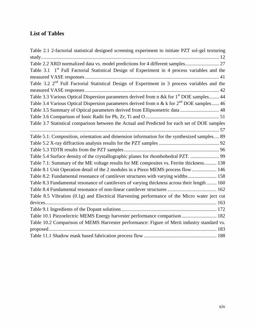
Figure 1.1 Zl/Y0 ratio, a measure of the ability to convert energy (Zl is the max energy harvester
displacement and Yo is the source vibration amplitude) vs. type of transduction vs. device size (©
IOP Publishing. Reproduced with permission. All rights reserved) .............................................. 2
Figure 2.1 Sol-gel process flow .................................................................................................... 11
Figure 2.2 A typical XRD plot from a PZT sol-gel thin film showing small (100), substantial
(110) and a large (111) shoulder (inset shows the whole spectrum on log scale). The film was
deposited on a platinized silicon substrate .................................................................................... 14
Figure 2.3 Half Normal probability plots of XRD responses – (100), (110) and (111) peak
heights ........................................................................................................................................... 14
Figure 2.4 Contour plots showing increasing trends with respect to annealing conditions for
(100) at 2θ = 22˚, (110) at 2θ = 31˚ and (111) at 2θ = 38; the Pyrolysis conditions were 300 oC
and 3 min....................................................................................................................................... 15
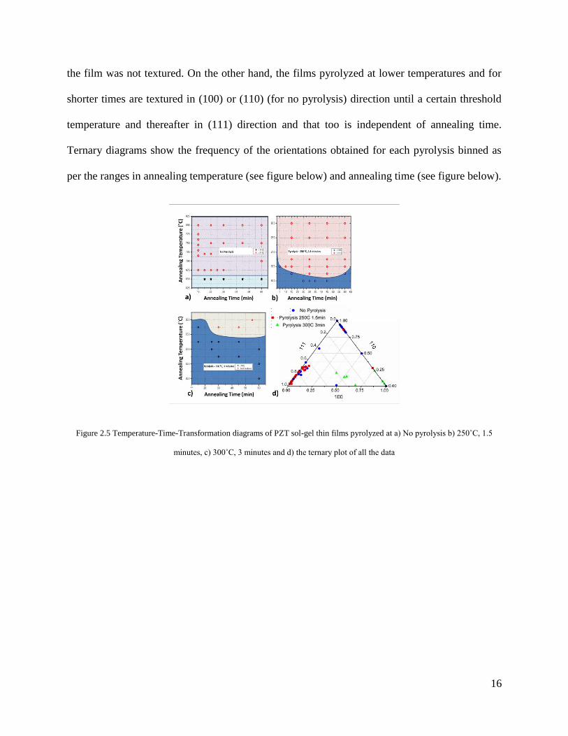
Figure 2.5 Temperature-Time-Transformation diagrams of PZT sol-gel thin films pyrolyzed at a)
No pyrolysis b) 250˚C, 1.5 minutes, c) 300˚C, 3 minutes and d) the ternary plot of all the data . 16
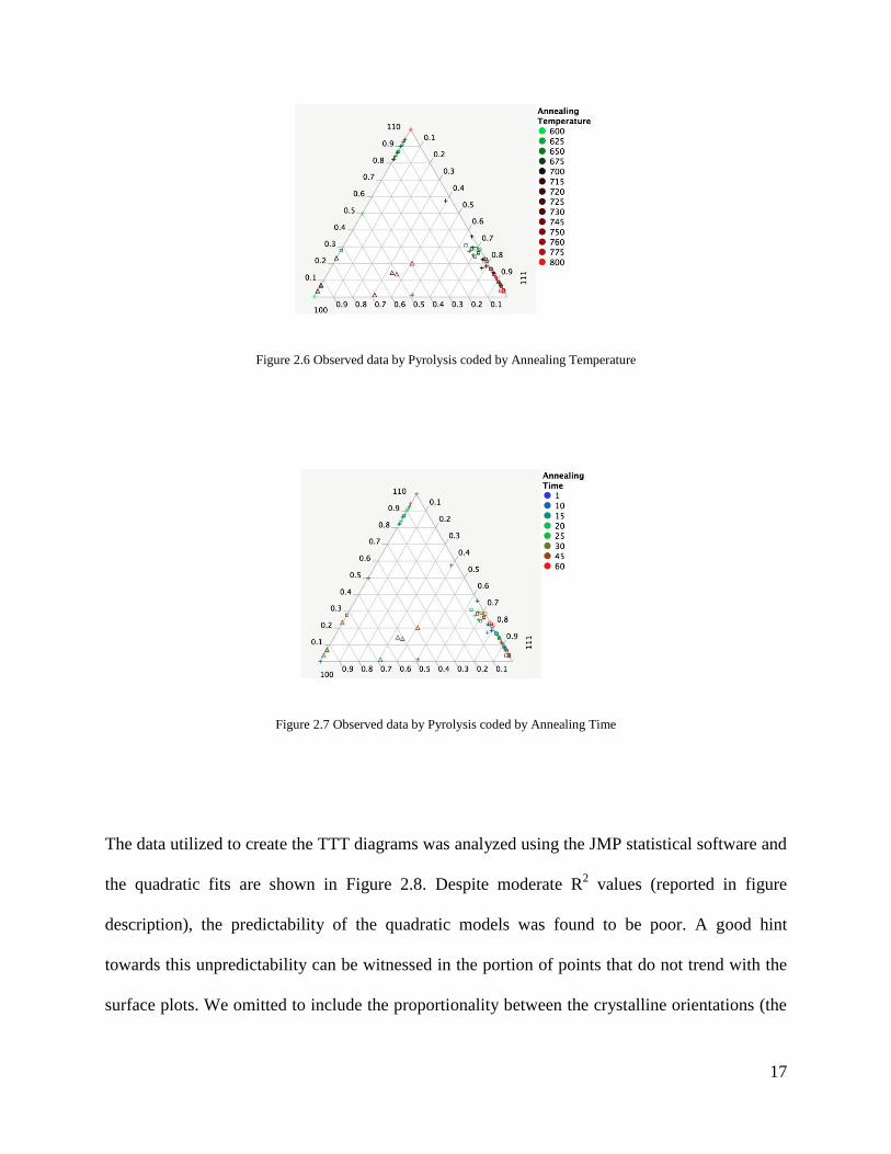
Figure 2.6 Observed data by Pyrolysis coded by Annealing Temperature ................................... 17
Figure 2.7 Observed data by Pyrolysis coded by Annealing Time ............................................... 17
Figure 2.8 JMP Contour plots of PZT sol-gel thin films pyrolyzed at a) No Pyrolysis – (100) with
R2 = 0.662, (110) with R
2 = 0.381 and (111) with R
2 = 0.644, b) 250˚C 1.5min Pyrolysis – (100)
with R2 = 0.495, (110) with R
2 = 0.451 and (111) with R
2 = 0.527and at c) 300˚C, 3min pyrolysis
– (100) with R2 = 0.722, (110) with R
2 = 0.961 and (111) with R
2 = 0.694 ................................. 18
Figure 2.9 JMP Scatter plot matrix of the responses (XRD peak data) vs. the factors - pyrolysis
and annealing conditions............................................................................................................... 19
Figure 2.10 Actual vs. Predicted for a) Multinomial Categorical b) Multinomial Continuous c)
Log-Ratio Categorical and d) Log-Ratio Continuous (blue-observed, red-fitted) models ........... 25
Figure 2.11 Actual vs. Fitted for a) (100),: b) ([110) and c) (111) ............................................... 26
Figure 2.12 Comparison of prediction results for 4 sol-gel samples ............................................ 28
Figure 3.1 (a) RF sputter configuration for PZT thin films, (b) PZT RF Sputter process variables,
and (c) EDX of PZT on platinized Si – on zooming in, Zr peak is buried under Pt peak ............ 36
Figure 3.2 Half Normal Probability plots of VASE responses – Thickness, refractive index ‘n’
and extinction coefficient ‘k’ for the 1st DOE .............................................................................. 42
Figure 3.3 Half Normal Probability plots– Thickness, Refractive Index ‘n’ and Extinction
coefficient ‘k’ for the 2nd
DOE ..................................................................................................... 43
Figure 3.4 (a) Tauc plot with inset showing the tangent line to x-axis to derive Eg, (b) Urbach
plot to derive Eu, (c) Jackson-Amer plot to determine sub-gap absorption and (d) Wemple-
DiDomenico plot to derive Eo and Ed ........................................................................................... 43
Figure 3.5 Scatterplot of Tauc Optical Gap Eg and Wemple-DiDomenico parameters Eo and Ed
vs. Atomic fractions ...................................................................................................................... 45

xi
Figure 3.6 Electronic polarizabilities vs. Atomic fractions for the 1st DOE - a) αm,r b) αrrr and c)
....................................................................................................................................................... 51
Figure 3.7 Predicted vs. Actual (EDX) Atomic fractions for the 1st DOE (dotted line depicts x=y)
....................................................................................................................................................... 53
Figure 3.8 Flowchart of Proposed methodology.......................................................................... 54
Figure 3.9 Electronic polarizabilities vs. Atomic fractions for the 2nd DOE - a) αm,r b) αrrr and
c) ................................................................................................................................................... 55
Figure 3.10 Predicted vs. Actual (EDX) Atomic fractions for the 2nd
DOE (dotted line depicts
x=y) ............................................................................................................................................... 56
Figure 4.1 Laser Doppler Vibrometry technique [14]. ................................................................. 63
Figure 4.2 a) \ Magnetostriction measurement setup and b) the schematic of the field and force
vectors ........................................................................................................................................... 64
Figure 4.3 a) Side-view and b) Top-view of the magnetostriction measurement setup ............... 66
Figure 4.4 Schematic of the induced curvature in sample due to applied magnetic force ........... 68
Figure 4.6 Magnetostriction (λ) calculated using equations 3-4 and 5 for a) NFO on Si
vs.Platinized Si b) NFO on Si as-deposited, after 650C and 750C anneal and c) CFO on
Platinized Si .................................................................................................................................. 74
Figure 4.7 M-H hysteresis loops for a) NFO on Si vs.Platinized Si b) NFO on Si as-deposited,
after 650C and 750C anneal and c) CFO on Platinized Si ............................................................ 76
Figure 5.1 Schematic diagram of the TDTR system. The pump beam heats the surface of the
sample and the time-delayed probe beam monitors changes in temperature at the sample surface.
Thermal conductivity and interface thermal conductance are extracted by comparing the
experimental data with an analytical thermal model. ................................................................... 88
Figure 5.2 Sensitivity analysis. (a) The best fit with all three unknown parameters. (b) If G1 is
increased by less than 10% the fit is clearly poor at short delay times. (c) if k is increased by
~10%, the fit is clearly poor at short and intermediate times. (d) if G2 is increased by ~15%, the
fit is poor for all delay times. ........................................................................................................ 91
Figure 5.4 High Resolution Binding energy XPS depth profiling of a PZT sol-gel thin film ...... 93
Figure 5.5 Optical dispersion data for all PZT samples used in this analysis .............................. 93
Figure 5.6 Raman shift data for the 3 highly textured PZT sol-gel thin films .............................. 94
Figure 5.7 a) High resolution TEM of a highly textured PZT sol-gel thin film. The Au and Pt on
the left side of the left panel were added to the sample during the lift-out process in preparation
for the TEM. EDS maps showing b) Ti distribution and c) Zr distribution across the PZT-Pt
interface......................................................................................................................................... 95
Figure 5.8 Ternary contour plot of thermal conductivity of PZT vs. crystallographic orientation
....................................................................................................................................................... 97
Figure 5.9 Ternary contour plot of interfacial thermal conductance a) G1 or GAl-PZT b) G1/k or
GAl-PZT /kPZT vs. crystallographic orientation. ............................................................................. 100
Figure 5.10 Ternary contour plot of interfacial thermal conductance a) G2 or GPZT-Pt b) G2/k or
GPZT-Pt/kPZT vs. crystallographic orientation. .............................................................................. 101

xii
Figure 6.1 a) Schematic and b) Components of PiezoCap Prototype 1 device (left to right) – d31
mode piezo MFC, ABS housing, d33 mode piezo MFC – and the device test setup ................. 111
Figure 6.2 a) Schematic and b) Components of PiezoCap Prototype 2 – 2 Quikpaks spaced apart
by ABS housing and held by clear plastic cylinders and the device test setup .......................... 113
Figure 6.3 a) Schematic and b) Components of PiezoCap Prototype 3 – 2 Quikpaks spaced apart
by and held by Brass washers and the device test setup ............................................................. 114
Figure 6.4 a) Velocity FRF and b) Voltage FRF for Prototype 1 ............................................... 116
Figure 6.5 Voltage and Power loading curves for a) P1 d33 MFC and b) P2 d31 MFC ............ 117
Figure 6.6 Separation of fundamental resonances in Prototype 2: bottom curve with magnets
without piezo and top with magnets on piezo ............................................................................. 118
Figure 6.7 The spring force diagrams for Prototype 1 on left and 2 on right ............................. 119
Figure 6.8 The resonant frequency variation with spacing between the magnets for the Nickel
neutral axis modified harvester ................................................................................................... 120
Figure 6.9 Variation in a) normalized resonance b) frequency shift c) 3dB bandwidth and d)
generated voltage difference for Prototype 3 .............................................................................. 122
Figure 6.10 Voltage and Power loading curves for Top and Bottom Quikpaks a) As is and b)
with Nickel neutral axis modifier in Prototype 3 ........................................................................ 125
Figure 7.1 a) Ferrite 40011 fired sheet and ME soldered composite with b) d31 mode electroding
using silver paste conductors and c) d33 mode electroding using Pt conductors. ....................... 131
Figure 7.2 Schematic of the fabrication process flow for ME macro fiber composite cantilever
..................................................................................................................................................... 132
Figure 7.3 a) diced ME composite b) IDE pattern for flexible circuit and c) final ME macro fiber
composite (ferrite of 0.5mm on left and 0.6mm on right). ......................................................... 133
Figure 7.4 Magnetoelectric test setup with translatable DC bias shown on the right side of the
figure. .......................................................................................................................................... 134
Figure 7.5 Magnetostriction results for Electroscience Type 40011 ferrite ............................... 135
Figure 7.6 Magnetoelectric voltage coefficient results for a) 0.5mm Ferrite and b) 0.6mm Ferrite
ME composites operating in d31 and d33 modes. ...................................................................... 137
Figure 7.7 Voltage and power loading curves for 0.5mm (top) and 0.6mm (bottom) ME
composite MFC’s. ....................................................................................................................... 139
Figure 7.8 a) Magnetization-Field (M-H) hysteresis loop for the Electroscience Ferrite 40011 and
b) the effective DC Magnetic bias achievable by using a longitudinally translatable NdFeB
magnet ......................................................................................................................................... 140
Figure 8.1 New Self aligned Mechanical First Electrical Last process ...................................... 148
Figure8.2 Vibration testing setup with perimeter clamping of MEMS wafer ............................ 149
Figure 8.3 Animation plots of the Velocity FRF at fundamental resonance of a) a linear zigzag
and b) a circular spiral................................................................................................................. 149
Figure 8.4 Electrical test setup: (clockwise from top left) PCB layout design, as manufactured,
with pogo pins soldered on and finally clamped over a device wafer ........................................ 151
Figure 8.5 XRD pattern of Inostek (red) vs. our Platinized Si ................................................... 152

xiii
Figure 8.6 a) sputtered PZT 52/48 and b) sol-gel PZT 60/40 on PbO sublimed over Inostek
platinized Si ................................................................................................................................ 153
Figure 8.7 Effect of Oxygen pre-annealing of our platinized Si on PZT texturing .................... 154
Figure 8.8 PZT texturing dependence on stoichiometry of the sputtering target ....................... 155
Figure 8.9 Effect of ALD thin films of Al2O3 and HfO2 on PZT texturing .............................. 156
Figure 8.10 Cantilevers with varying widths and a Bezier at clamped end ................................ 157
Figure 8.11 a) Flat b) Angled and c) 50” Radius of curvature beam .......................................... 160
Figure 8.12: Proposed methodology to tune the frequency of partially or fully manufactured
MEMS structures with tip mass .................................................................................................. 161
Figure 8.13 Silicon MEMS cantilever structures a) As fabricated b) CAD-generated .............. 161
Figure 8.14 Micro water jet cut Piezo sheets – 4 turn Circular Zigzag on left and 5 turn on right
..................................................................................................................................................... 162
Figure 8.15 Power Loading curves for Piezo a) sheet b) unimorph (note the different Ni thickness
used for each CZ structure) and c) bimorph ............................................................................... 165
Figure 8.16 Chevron interdigitated electrode pattern for d33 mode energy harvesting ............. 166
Figure 9.1 SEM of a) undoped ANI Copper ink vs. b) doped Copper ink sample E ................. 174
Figure 9.2 XRD data for a) undoped Copper and b) E-doped Copper after 3 anneals vs c)
undoped ink air dried .................................................................................................................. 176
Figure 10.1 Ball Harvester concept using PiezoCap technology ................................................ 185
Figure 11.1 Schematic of a Single Layer Transformer structure ................................................ 187
Figure 11.2 Shadow mask processing using metal shadow mask and magnets (to protect
electrical pads from deposition) .................................................................................................. 188
Figure 11.3 Electrical connections and equipment for High Frequency ME testing – a) DUT
(device under test), b) impedance testing schematic, c) Gain testing schematic, d) test bench and
e) probe tip with special wired tethers for common ground ....................................................... 189
Figure 11.4 Unipoled transformer stack with the backside Si removed (shown in lower part) . 190
Figure 11.5 Configuration of Piezo MFC parallel to wind tunnel with free end away from flow
..................................................................................................................................................... 191
Figure 11.6 Results of a Piezo MFC with a 45 degree plate upstream (clockwise from top left):
Comparison between P1 d33 and P2 type d31MFC’s, Dominant frequencies for P1 vs. P2 vs.
orientation and typical Voltage FRF ........................................................................................... 192
Figure 11.7 Results of a Piezo MFC with a rotating plate upstream (clockwise from top left):
Comparison between P1 d33 and P2 type d31MFC’s, Dominant frequencies for P1 vs. P2 vs.
orientation and typical Voltage FRF ........................................................................................... 193
xiv
List of Tables
Table 2.1 2-factorial statistical designed screening experiment to initiate PZT sol-gel texturing
study .............................................................................................................................................. 12
Table 2.2 XRD normalized data vs. model predictions for 4 different samples ........................... 27
Table 3.1 1st Full Factorial Statistical Design of Experiment in 4 process variables and the
measured VASE responses ........................................................................................................... 41
Table 3.2 2nd
Full Factorial Statistical Design of Experiment in 3 process variables and the
measured VASE responses ........................................................................................................... 42
Table 3.3 Various Optical Dispersion parameters derived from n &k for 1st DOE samples ........ 44
Table 3.4 Various Optical Dispersion parameters derived from n & k for 2nd
DOE samples ...... 46
Table 3.5 Summary of Optical parameters derived from Ellipsometric data ............................... 48
Table 3.6 Comparison of Ionic Radii for Pb, Zr, Ti and O ........................................................... 51
Table 3.7 Statistical comparison between the Actual and Predicted for each set of DOE samples
....................................................................................................................................................... 57
Table 5.1: Composition, orientation and dimension information for the synthesized samples. ... 89
Table 5.2 X-ray diffraction analysis results for the PZT samples ................................................ 92
Table 5.3 TDTR results from the PZT samples ............................................................................ 96
Table 5.4 Surface density of the crystallographic planes for rhombohedral PZT. ....................... 99
Table 7.1: Summary of the ME voltage results for ME composites vs. Ferrite thickness .......... 138
Table 8.1 Unit Operation detail of the 2 modules in a Piezo MEMS process flow .................... 146
Table 8.2: Fundamental resonance of cantilever structures with varying widths ....................... 158
Table 8.3 Fundamental resonance of cantilevers of varying thickness across their length ........ 160
Table 8.4 Fundamental resonance of non-linear cantilever structures ....................................... 162
Table 8.5 Vibration (0.1g) and Electrical Harvesting performance of the Micro water ject cut
devices......................................................................................................................................... 163
Table 9.1 Ingredients of the Dopant solutions ............................................................................ 172
Table 10.1 Piezoelectric MEMS Energy harvester performance comparison ............................ 182
Table 10.2 Comparison of MEMS Harvester performance: Figure of Merit industry standard vs.
proposed ...................................................................................................................................... 183
Table 11.1 Shadow mask based fabrication process flow .......................................................... 188

1
Chapter 1
Introduction
Scope, Purpose and Significance of Research
Energy harvesting is the field in which various transduction mechanisms are utilized to convert
excess or vestigial sources of energy into useful energy. Vibrational energy is one of the most
common sources of ambient waste energy. Piezoelectric and electromagnetic transduction
schemes are the most popular for vibrational energy conversion. Miniaturization of wireless
sensors, autonomous electronic systems and harsh environment or remote sensor nodes require
the scaling down of energy harvesters to the MEMS scale.
Figure 1.1 delineates the range of operation of piezoelectric MEMS vs. the electromagnetic
energy harvester[1]. With decrease in size, piezoelectric MEMS devices become the preferred
mode of transduction.
2
Figure 1.1 Zl/Y0 ratio, a measure of the ability to convert energy (Zl is the max energy harvester displacement and Yo is the
source vibration amplitude) vs. type of transduction vs. device size (© IOP Publishing. Reproduced with permission. All rights
reserved)
A piezoelectric MEMS harvester comprises of a Piezo thin film element on an elastic cantilever
which transfers the source vibration into the device. Therefore, the fabrication of such a device
includes the development and characterization of the piezoelectric thin film, the development
and fabrication of the MEMS cantilever structure and finally the MEMS device characterization.
In this research, we explore different concepts of Energy Harvester devices from the perspective
of structural resonance frequency, band width of operation, ease of manufacturability, tunability
and versatility. With the addition of a magnetostrictive layer, the Piezo MEMS can double as a
Magnetoelectric MEMS harvester.
Most vibrational sources of energy in nature and industry have a frequency signature < 1kHz.
Often these ambient frequencies are in the < 100Hz range and therefore, the focus of most
MEMS energy harvesting research has been to achieve that level of operation. As the
fundamental frequency of a simple cantilever beam is given as , where k is the stiffness
3
(proportional to ) and m is the mass (proportional to
), when dimensions reduce to micron sizes, the natural frequency
of a simple cantilever scale higher than that in the macro scale. Therefore, considerable emphasis
in research has been placed in discovering low frequency structures in the MEMS scale. These
structures tend to have non-standard and non-linear shapes that are attuned for low frequency
vibrational energy transfer.
Dissertation Structure
The active element in a Piezoelectric or Magnetoelectric MEMS device is the piezoelectric thin
film which in our case is PZT, Lead Zirconium Titanate. We therefore delved into the
development of PZT thin film by sol-gel spin coating and RF sputtering techniques. For the
magnetostrictive component, we developed NFO, Nickel Ferrite, thin films by RF sputtering.
During the detailed characterization of these films, we discovered some gaps in existing
metrology and predictive data modeling and proceeded to resolve them.
The first area of derivative research was in Ceramic Data Analytics of Pb(Zr0.60Ti0.40 O3) sol-gel
thin films. We describe an analytical model to define the temperature-time-transformation (TTT)
diagram of sol-gel deposited Pb(Zr,Ti)O3 thin films on platinized silicon substrates. Texture
evolution in film occurred as the pyrolysis and thermal annealing conditions were varied. We
demonstrate that the developed model can quantitatively predict the outcome of thermal
treatment conditions in terms of texture evolution. Multinomial and multivariate regression
techniques were utilized to create the predictor models for TTT data. Further, it was found that

4
multinomial regression can provide better fit as compared to standard regression and multivariate
regression. We have generalized this approach so that it can be applied to other thin film
deposition techniques and bulk ceramics.
The second area of derivative research was in Photo Elemental Analysis of Pb(Zr0.52Ti0.48 O3) RF
sputtered thin films. This work provides the correlation between the compositions of a given thin
film to its optical dispersion properties. Gladstone-Dale (G-D) relationships have been used in
optical mineralogy to relate density of crystalline compounds to their average refractive index.
We purport to use a ‘reverse’ G-D approach and determine the composition of multi-component
thin films from their optical properties. As a model system, we focused on complex perovskite
ferroelectric thin film and applied the derived relationship to determine the stoichiometry. The
wavelength dispersion of refractive index and extinction coefficient of various Pb(Zr,Ti)O3
(PZT) thin films was measured using Variable Angle Spectroscopic Ellipsometry (VASE).
Elemental compositions were measured using Energy Dispersive X-ray analysis (EDX) and
Electron Probe Micro Analysis (EPMA). Wemple-DiDomenico, Jackson-Amer, Tauc and
Urbach optical relationships were used to extract correlations to elemental content. Also,
theoretical and semi-empirical approaches to calculate the electronic polarizability of PZT were
employed and their variation with elemental content was computed. Perovskite tolerance and
octahedral factors were also analyzed against the optical and polarizability parameters. These
factors and relationships were combined to realize a model for predicting the elemental content
of a thin film system.
A third area of derivative research was in the development of in house capability for strain
analysis of magnetostrictive thin films. As we are well equipped to measure vibrations using
laser Doppler Vibrometry (LDV), we embarked on determining a methodology to convert the

5
displacements measurements of AC magnetic field induced vibration of thin film samples into
magnetostriction values.
A fourth area of derivative research was in the quest for a materials characterization technique to
detect differences in interfacial layers of a few atomic layers. These atomic layers are claimed to
determine texturing of PZT thin films grown over platinized Si substrates. After futile attempts at
using Raman Scattering, FTIR, TEM and XRD techniques, we were unable to settle on a well-
established materials characterization technique that had the spatial resolution and the sensitivity
to detect these texturing atomic layers. Time Domain Thermoreflectance (TDTR) has been
proven to be capable of measuring thermal properties of atomic layers and especially that at
interfaces. Therefore, we explored the use of TDTR to correlate with PZT texturing trends.
Chapter 6-7 will introduce device designs and concepts for energy harvesting in and with
alternating magnetic fields and vibrations. The straightforward concept is to take the Piezo
MEMS described in Chapter 8 and apply a magnetostrictive layer like Nickel Ferrite (NiFe2O4)
over the Piezo capacitor. Another tactic employed is the development of energy harvesting
concepts that will fit in the same foot print of a fully packaged MEMS device but circumvents
intensive and sensitive wafer processing. A MEMS device requires special vacuum packaging to
prevent damage and minimize air damping. For the most low frequency MEMS structures, the
package can extend to dimensions of almost 25mm x 25mm x 20mm. In such a volume, we can
supplement the wafer based MEMS approach with non-wafer based solutions. On the non-wafer
side, we developed a MEMS scalable prototype of a) a magnetically levitated system with
piezoelectric macro fiber composite harvesters and b) a magnetoelectric macro fiber composite
(ME MFC) simple cantilever. The former, called PiezoCap, delivered on its design objectives
and then made one giant leap forward by revealing to us a methodology to make vibration piezo
6
harvesters non-dimensional. PiezoCap resonance frequency is tuned purely by magnetic stiffness
force. The ME MFC was developed with better magnetoelastic coupling to the piezo realized by
using a low temperature solder bonding process between the magnetostrictive ferrite and the
piezo.
Chapter 8 describes the approach undertaken to achieve a low frequency Piezo MEMS
energy harvester. The study of various cantilevered structures to determine the path to attain low
frequency. We describe our unique fabrication methodology to realize these structures. We also
describe the extensive work that went into MEMS wafer test bench setup. A circular labyrinth
structure was proven to achieve <100Hz resonant energy harvesting operation whilst generating
ample power at low acceleration of 0.1g. Micro water jet cutting is introduced as a bulk Piezo
micromachining technique.
Chapter 9 divulges methodologies to improve the oxidation resistance of copper ink for
direct writing purposes. We utilize technology from the dispersion strengthening of copper to do
so without adversely affecting electrical conductivity.
Chapter 11 will divulge studies completed on a) the additive fabrication methodology for
Piezo thin film based transformers and b) flow induced vibration energy harvesters.
References
[1] Mitcheson PD, Reilly EK, Toh T, Wright PK, Yeatman EM. Performance limits of the
three MEMS inertial energy generator transduction types. Journal of Micromechanics and
Microengineering 2007;17:S211.
7
Chapter 2
Temperature-time Transformation Diagram for
Pb(Zr,Ti)O3 Thin Films 1
Ronnie Varghese, Matthew Williams1, Shashaank Gupta, and Shashank Priya
*
Center for Energy Harvesting Materials and Systems (CEHMS), Department of Materials Science and Engineering, Virginia Tech, Blacksburg,
VA 24061.
1Department of Statistics, Virginia Tech, Blacksburg, VA 24061.
Abstract
In this paper, we describe an analytical model to define the temperature-time- transformation
(TTT) diagram of sol-gel deposited Pb(Zr,Ti)O3 thin films on platinized silicon substrates.
Texture evolution in film occurred as the pyrolysis and thermal annealing conditions were
varied. We demonstrate that the developed model can quantitatively predict the outcome of
thermal treatment conditions in terms of texture evolution. Multinomial and multivariate
regression techniques were utilized to create the predictor models for TTT data. Further, it was
found that multinomial regression can provide better fit as compared to standard regression and
multivariate regression. We have generalized this approach so that it can be applied to other thin
film deposition techniques and bulk ceramics.
Keywords: Thin films; piezoelectric ; texturing; multiple regression
1 Reprinted with permission from [J. Appl. Phys. 110, 014109 (2011)]. Copyright [2011], AIP Publishing LLC
8
Introduction
Pb(Zr,Ti)O3 (PZT) thin films deposited using sol-gel process, a chemical solution deposition
(CSD) technique, are frequently used in micro-electronics industry. This industry focus has lead
to detailed studies on the effect of sol-gel process variables on texturing of PZT films. It is well-
known that piezoelectric properties are maximized along certain crystallographic direction
depending upon the parent phase symmetry. To exemplify, <001> oriented single crystals of
morphotropic phase boundary composition 0.92 Pb(Zn1/3Nb2/3)O3 – 0.08PbTiO3 (PZNT) have
been shown to possess high electromechanical coupling coefficients of 0.94, high piezoelectric
constants of between 2000 and 2500 pC/N
and high electrically induced strains of
1.7%.[1],[2],[3],[4]
Park and Shrout attributed this high electromechanical performance to domain
engineered state achieved through polarization rotation from <111> to <001>.[3],[4]
First
principles calculations have indicated that the transformation under electric field between
ferroelectric rhombohedral and ferroelectric tetragonal phases proceeds by rotation of the
polarization between <111> and <001>, via the <110>.[5] This rotation causes a large coupling
between the polarization and electric field causing a giant piezoresponse. In general, a
rhombohedral composition oriented along <100> direction and a tetragonal composition oriented
along <111> direction will exhibit optimum magnitude of electromechanical coefficients[6].
Thus, texturing is desired in PZT but poses several challenges in synthesis. The growth of bulk
PZT in single crystal or textured form has been difficult due to the incongruent melting of ZrO2.
However, PZT films can be textured due to the low annealing temperature required to achieve
proper crystallinity. The questions which we pose in this study are: “How to predict the texture
of sol-gel deposited PZT thin films with high degree of confidence?”; and “Can a generalized

9
mathematical model be developed for predicting the texture in ferroelectric materials in terms of
synthesis parameters for any given synthesis process?”.
There are numerous variables in sol-gel deposition process including choice of bottom electrode,
interfacial layers, precursor chemistry and concentration, solvent, chelating agents, dilution rate
(determined by molarity and effects viscosity of sol), hydrolysis ratio, spin coating speed and
times, and pyrolysis and annealing conditions (including ramp up and down rates)[7]. The
innumerability of the variables presents the difficulty in optimizing the conditions for achieving
high texture degree. Further, it makes the deposition process susceptible to human errors. This is
evident from the fact that a large pool of data exists in literature on sol-gel deposition of PZT
thin films but the research has shown that there exists significant variation in the measured
results across the laboratories. For repeatability, current methodology requires detailed
documentation of process conditions and procedures and access to similar type of equipment and
starting material. The situation becomes more complex when one is looking for specific texture
in the deposited film. This describes the motivation behind our study. We focus on developing
mathematical criterion for predicting the texture in sol-gel deposited thin films by fixing many of
the variables and just varying the pyrolysis and thermal annealing conditions. These two
variables are most commonly used to modulate the phase of the films and thus we could refer to
them as “texture controlling parameters” (TCP).
In PZT sol-gel studies, Temperature-Time-Transformation (TTT) diagrams have been developed
to represent the variation of texture as a function of TCP[8]. These diagrams are commonly
invoked to understand the texturing mechanisms[9],[10]
and quantify the operating regime for
achieving specific orientation. However, these diagrams are just pictorial guides specific to a
given sol-gel deposition process. Besides, these guides can be misleading as they can only depict
10
the dominant crystalline phase or texture and do not provide the reader with an understanding of
the extent of the other mixture of phases. Mathematical modeling of the TCP data has never been
attempted and therefore, no predictor models are available. This paper attempts to fill that void
by proposing a statistical methodology to predict the crystalline orientation. The ability to define
the boundaries in terms of TCP will allow repeatability in synthesis of textured films.
Polycrystalline thin films can have one or two predominant crystalline orientation. Compiling
XRD data from several samples can lead to binary trends, that is, higher the texturing in one
orientation lower it is in the other possible orientations. In case of PZT 60/40 (where Zr = 0.60
and Ti = 0.40 mol fraction) thin films, the three dominant textures are <100>, <110> and <111>
and therefore the data can be considered trinomial and interdependent. Standard multiple
regression methods cannot adequately describe these interdependent responses and so
multivariate regression is recommended. But multivariate regression approaches can be
complicated and difficult. Thus, a non-linear simultaneous or multinomial regression approach is
proposed and compared to consecutive multiple and simultaneous multivariate linear regression
approaches.
Experimental Procedure
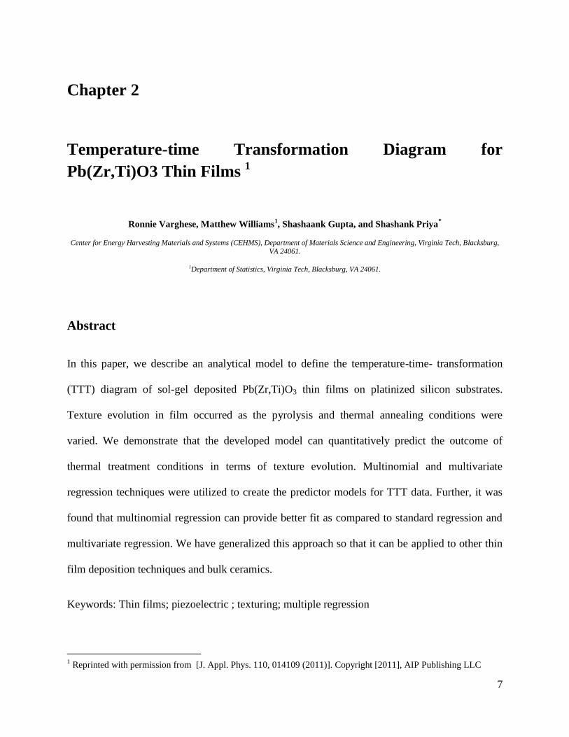
The sol-gel deposition process was optimized from that described in Reference [11] and consists
of the following steps (see figure below): (1) preparation of the sol from Pb, Zr and Ti precursors
in a glove box, (2) spin coating of the sol onto the substrate, (3) pyrolysis of the sol-gel thin film
on a hot plate to remove solvents and organics and, (4) densification and crystallization of the
thin film in a high temperature tube furnace. The mixture of individual sols results in a final
composition of 0.4M Pb1.1(ZrxTi1-x)O3 with x = 0.6. An extra 10% Pb was included to
11
compensate for the losses during thermal treatments as PbO has high vapor pressure of 2Torr at
700oC.
Figure 2.1 Sol-gel process flow
The lead sol comprises of lead acetate trihydrate 99.99% diluted in 2-methoxymethanol 99.9%
solvent. The lead sol was dehydrated at 100oC for 2hrs. The zirconium + titanium sol (henceforth
referred to as ZT) was created by first mixing Zr (IV) propoxide 70% in 1-proponal solvent (1-
propanol 99%) at room temperature. After a few minutes of mixing, Ti (IV) propoxide 97% was
added, mixed, followed by addition of acetyl acetonate, a chelating agent. The third sol was the
hydrolysis sol comprising of the deionized water (> 18 Mohms) with 1-propanol 99% in equal
ratios. After the lead sol has cooled down to room temperature, the ZT sol was added to it while
stirring at 250rpm. After one hour of stirring, the hydrolysis sol was added slowly and after four
more hours of stirring, the clear sol was aged for twenty four hours. The aged sol was then spun
12
onto platinized silicon substrates (Pt/Ti/SiO2/Si) at 3500rpm for 30 sec. After spin coating, the
thin films were pyrolyzed and annealed as per table below. Table 2.1 depicts a 24 full factorial
screening experiment in the four factors (TCP) – pyrolysis time, pyrolysis temperature, annealing
time and annealing temperature. Pyrolysis was conducted on a hot plate whilst annealing was
accomplished in a vertical furnace exposed to ambient air. The resultant thin film thickness was
in the range of 65-85nm.
Table 2.1 2-factorial statistical designed screening experiment to initiate PZT sol-gel texturing study
Name Units Type Low Actual High Actual
Pyrolysis temperature oC Numeric 250 350
Pyrolysis time min. Numeric 1.5 4.5
Annealing temperature oC Numeric 650 750
Annealing time min. Numeric 10 20
The gelation process of pyrolysis and perovskite crystallization process of annealing were
optimized for 3 different textures ((100), (110) and (111)) of PZT thin films on platinized silicon
substrates. Subsequent detailed experimentation included the investigation on thermal budget to
identify all the regions on operating space and the data from these samples was used to
rigorously fill the TTT diagram for three different crystalline orientations. For the screening
experiments, platinized silicon substrates from Nova Electronic Materials, FlowerMound, TX,
were used and to develop the TTT diagrams followed by more detailed experiments, substrates
from Inostek, South Korea, were utilized. The former had a micron of Pt over a Ti glue layer on
SiO2/ Si whilst the latter had the configuration of 150nm Pt/10nm Ti/300nm SiO2/Si. X-ray
diffraction was used to measure the orientation of the thin films. The X-ray peak heights
13
(alternatively FWHM can be employed too) were measured and normalized. Design Expert
software was used to generate and analyze the statistically designed screening experiments
(SDE). JMP and R software’s were used in the mathematical modeling of the TTT data.
Results and Discussion
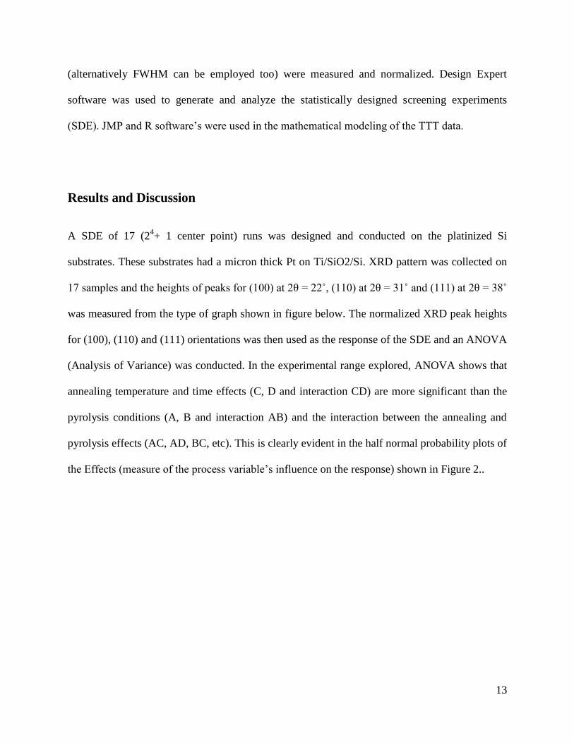
A SDE of 17 (24+ 1 center point) runs was designed and conducted on the platinized Si
substrates. These substrates had a micron thick Pt on Ti/SiO2/Si. XRD pattern was collected on
17 samples and the heights of peaks for (100) at 2θ = 22˚, (110) at 2θ = 31˚ and (111) at 2θ = 38˚
was measured from the type of graph shown in figure below. The normalized XRD peak heights
for (100), (110) and (111) orientations was then used as the response of the SDE and an ANOVA
(Analysis of Variance) was conducted. In the experimental range explored, ANOVA shows that
annealing temperature and time effects (C, D and interaction CD) are more significant than the
pyrolysis conditions (A, B and interaction AB) and the interaction between the annealing and
pyrolysis effects (AC, AD, BC, etc). This is clearly evident in the half normal probability plots of
the Effects (measure of the process variable’s influence on the response) shown in Figure 2..
14
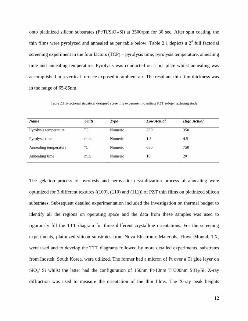
Figure 2.2 A typical XRD plot from a PZT sol-gel thin film showing small (100), substantial (110) and a large (111) shoulder
(inset shows the whole spectrum on log scale). The film was deposited on a platinized silicon substrate
Figure 2.3 Half Normal probability plots of XRD responses – (100), (110) and (111) peak heights
15
Figure 2.4 Contour plots showing increasing trends with respect to annealing conditions for (100) at 2θ = 22˚, (110) at 2θ = 31˚
and (111) at 2θ = 38; the Pyrolysis conditions were 300 oC and 3 min
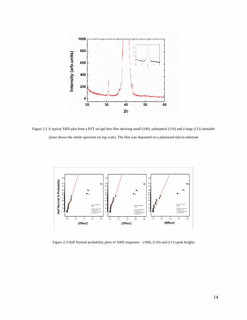
The resultant regression models generated the contour plots shown in figure above. We find that
higher annealing time and temperature yields higher desired peak (100) and decreases the
undesired peak (111). However, the (110) peak also increases in this process regime. These XRD
peaks were independent of pyrolysis time and temperature in the range explored. Also below
700oC, longer annealing times will make the peak height independent of annealing time. Using
this information, further extensive exploration of the sol-gel thermal budget operating space
yielded the TTT diagrams shown in figure below. This diagram is similar to that developed by
Chen and Chen[8, 9] except that their main process variables were pyrolysis temperature and
time and they had maintained annealing temperature and time constant. It can be seen that films
with pyrolysis at 300oC for 3 min were textured in (100) direction until ~ 750
oC annealing
temperature, after which they start showing random orientation (labeled ‘not textured’ in figure
below). This trend is a confirmation of the contour plot trends observed in the screening
experiments. With increase in annealing temperature and time, the (100) and (110) orientations
increases whilst (111) orientation decreases and at > 750oC, all three orientation co-exist and so
16
the film was not textured. On the other hand, the films pyrolyzed at lower temperatures and for
shorter times are textured in (100) or (110) (for no pyrolysis) direction until a certain threshold
temperature and thereafter in (111) direction and that too is independent of annealing time.
Ternary diagrams show the frequency of the orientations obtained for each pyrolysis binned as
per the ranges in annealing temperature (see figure below) and annealing time (see figure below).
Figure 2.5 Temperature-Time-Transformation diagrams of PZT sol-gel thin films pyrolyzed at a) No pyrolysis b) 250˚C, 1.5
minutes, c) 300˚C, 3 minutes and d) the ternary plot of all the data
17
Figure 2.6 Observed data by Pyrolysis coded by Annealing Temperature
Figure 2.7 Observed data by Pyrolysis coded by Annealing Time
The data utilized to create the TTT diagrams was analyzed using the JMP statistical software and
the quadratic fits are shown in Figure 2.8. Despite moderate R2 values (reported in figure
description), the predictability of the quadratic models was found to be poor. A good hint
towards this unpredictability can be witnessed in the portion of points that do not trend with the
surface plots. We omitted to include the proportionality between the crystalline orientations (the
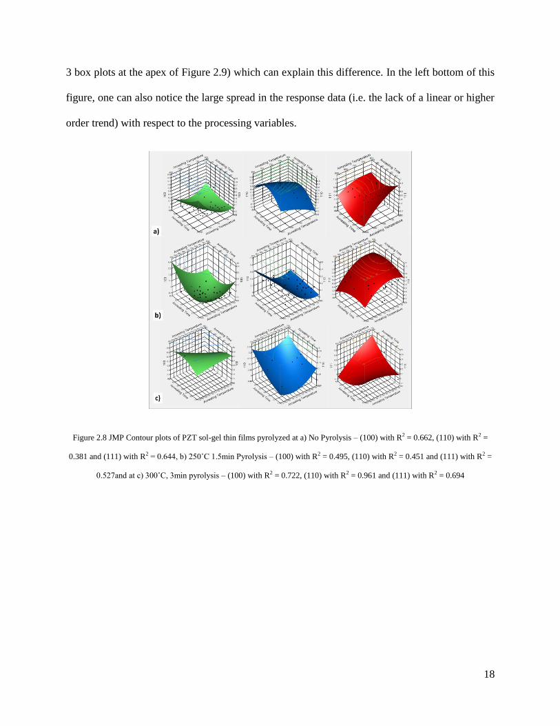
18
3 box plots at the apex of Figure 2.9) which can explain this difference. In the left bottom of this
figure, one can also notice the large spread in the response data (i.e. the lack of a linear or higher
order trend) with respect to the processing variables.
Figure 2.8 JMP Contour plots of PZT sol-gel thin films pyrolyzed at a) No Pyrolysis – (100) with R2 = 0.662, (110) with R2 =
0.381 and (111) with R2 = 0.644, b) 250˚C 1.5min Pyrolysis – (100) with R2 = 0.495, (110) with R2 = 0.451 and (111) with R2 =
0.527and at c) 300˚C, 3min pyrolysis – (100) with R2 = 0.722, (110) with R2 = 0.961 and (111) with R2 = 0.694

19
Figure 2.9 JMP Scatter plot matrix of the responses (XRD peak data) vs. the factors - pyrolysis and annealing conditions
Multiple regression takes a single response (or several separately ones at a time) and models its
relationship to multiple independent factors. The quadratic model, which is a multiple regression,
was inadequate to explain correlated response data evocative of XRD pattern data. To model this
joint relationship, a multivariate regression approach had to be employed. Multivariate
regression simultaneously relates several responses to each other and to multiple independent
factors. As mentioned earlier, the XRD peak data was normalized and so the three responses add
up to one and therefore are inherently related (i.e. not independent). Therefore we must model
them simultaneously. As pyrolysis conditions were lumped into three pairs of temperature and
time combinations in the TTT experimentation, each pair was considered as a single categorical

20
process variable. The other two process variables were considered as either categorical or
continuous variable in the regression.
After separate independent regressions (the aforementioned quadratic regression), two other
methods of regression, multinomial logistic[12] and log ratio multivariate[13], were evaluated.
For multinomial regression, we convert the normalized XRD data into counts. Bearing in mind
that the normalized data are the observed proportions of crystalline orientations in each film or
sample, then the 100 points or counts can be the sum total of all three crystalline orientations.
For example, if we observed percentages of 5%, 10%, and 85%, we would assign counts of 5,
10, and 85 respectively. Now we treat this transformed data as observed counts from a
multivariate binomial (multinomial) distribution. Our multinomial distribution is described by
three parameters representing the true unordered proportions in our mixture: p[100]; p[110];
p[111] with p[100] + p[110] + p[111] = 1. In order to perform regression to model these
parameters we use
(1) below:
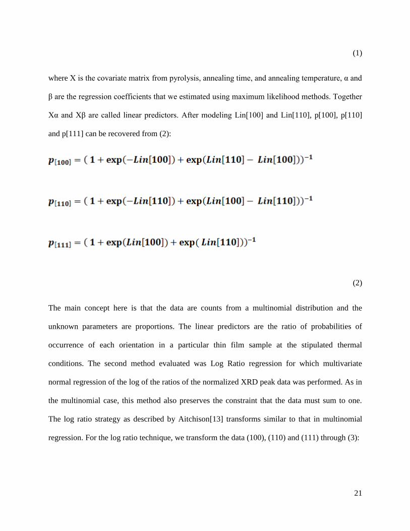
21
(1)
where X is the covariate matrix from pyrolysis, annealing time, and annealing temperature, α and
β are the regression coefficients that we estimated using maximum likelihood methods. Together
Xα and Xβ are called linear predictors. After modeling Lin[100] and Lin[110], p[100], p[110]
and p[111] can be recovered from (2):
(2)
The main concept here is that the data are counts from a multinomial distribution and the
unknown parameters are proportions. The linear predictors are the ratio of probabilities of
occurrence of each orientation in a particular thin film sample at the stipulated thermal
conditions. The second method evaluated was Log Ratio regression for which multivariate
normal regression of the log of the ratios of the normalized XRD peak data was performed. As in
the multinomial case, this method also preserves the constraint that the data must sum to one.
The log ratio strategy as described by Aitchison[13] transforms similar to that in multinomial
regression. For the log ratio technique, we transform the data (100), (110) and (111) through (3):

22
(3)
Thus the new data are LR1 and LR2 with mean vector (μ1; μ2) and covariance matrix S. In order
to perform regression we use (4):
(4)
After modeling μ1 and μ2, we can recover the fitted (predicted) concentrations with (5):
23
(5)
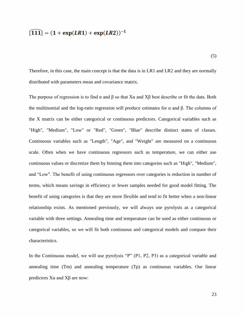
Therefore, in this case, the main concept is that the data is in LR1 and LR2 and they are normally
distributed with parameters mean and covariance matrix.
The purpose of regression is to find α and β so that Xα and Xβ best describe or fit the data. Both
the multinomial and the log-ratio regression will produce estimates for α and β. The columns of
the X matrix can be either categorical or continuous predictors. Categorical variables such as
"High", "Medium", "Low" or "Red", "Green", "Blue" describe distinct states of classes.
Continuous variables such as "Length", "Age", and "Weight" are measured on a continuous
scale. Often when we have continuous regressors such as temperature, we can either use
continuous values or discretize them by binning them into categories such as "High", "Medium",
and “Low". The benefit of using continuous regressors over categories is reduction in number of
terms, which means savings in efficiency or fewer samples needed for good model fitting. The
benefit of using categories is that they are more flexible and tend to fit better when a non-linear
relationship exists. As mentioned previously, we will always use pyrolysis as a categorical
variable with three settings. Annealing time and temperature can be used as either continuous or
categorical variables, so we will fit both continuous and categorical models and compare their
characteristics.
In the Continuous model, we will use pyrolysis “P” (P1, P2, P3) as a categorical variable and
annealing time (Tm) and annealing temperature (Tp) as continuous variables. Our linear
predictors Xα and Xβ are now:

24
(6)
Notice that “P” and all α's and β's associated with “P” change depending on whether P = P1, P2,
and P3. Since pyrolysis (P) can take on three values, we are fitting three models at the same time.
(7)
In the Categorical Model we treat Tm and Tp as categories. Our linear predictors’ form remains
the same but there are fewer interaction terms (Eq. ((7)). In this case, we fit a separate model for
each P, Tm, and Tp combination. If we had 5 levels of Tm, 5 levels of Tp, and 3 levels for P, we
would have 75 models that we estimate at the same time.
25
Figure 2.10 Actual vs. Predicted for a) Multinomial Categorical b) Multinomial Continuous c) Log-Ratio Categorical and d) Log-
Ratio Continuous (blue-observed, red-fitted) models
We used continuous and categorical models of both the multinomial and the log ratio methods to
fit the data. We then compared them to the observed data and the saturated categorical model
(which is essentially the same or a point by point fit). From Figure 2.(a) – (d) we see that the
categorical models have better fits than the continuous ones, suggesting a possible nonlinear
relationship in the predictor. Also, it seems that the multinomial model has a better fit than the
log ratio model. This is confirmed when plotting observed versus fitted data for each (100),
(110), (111) orientations separately in Figure 2.(a) – (c). Besides the saturated model, which is
26
not a realistic model (unless we have replicates), the categorical model with the multinomial data
(2nd from the left) gives the closest fit to the one-to-one line for the observed and fitted values.
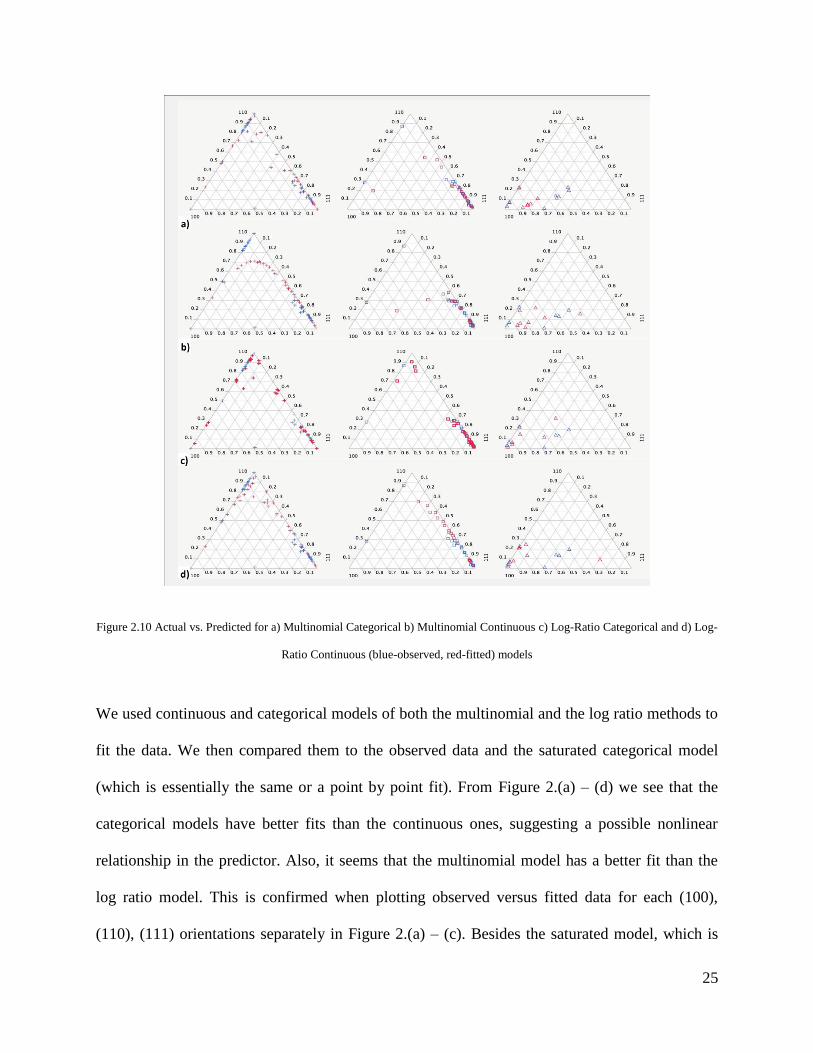
Figure 2.11 Actual vs. Fitted for a) (100),: b) ([110) and c) (111)
In using the multinomial model with categorical factors for prediction, the choice of annealing
temperature and time is restricted to that used in the original model whilst with continuous
factors, any annealing temperature and time value (but within the range used in the model) is
permitted. To elucidate (refer to Figure 2. and Figure 2.), with the continuous model one can
27
predict the response for an annealing temperature of 685˚C and 22 min but for the categorical
model (where discretized fixed values of the factors are used), we have to use an annealing
temperature and time that have been used in the original regression (say, 675˚C or 700˚C and 20
or 25min but not necessarily the same original combination of the two factors).
Table 2.2 XRD normalized data vs. model predictions for 4 different samples
Sample Pyrolysis &
Annealing
Conditions
XRD peak Actual Multinomial
Categorical
Model
Multinomial
Continuous
Model
Log-Ratio
Categorical
Model
Log-Ratio
Continuous
Model
SG1 300C 3min (100) 0.88 0.924 0.878 0.928 0.952
675C 30min (110) 0.12 0.076 0.0417 0.0721 0.0428
(111) 0 4.29E-06 0.08 0.0003 0.0056
SG2 300C 3min (100) 0.896 0.924 0.878 0.928 0.952
675C 30min (110) 0.104 0.076 0.0417 0.0721 0.0428
(111) 0 4.29E-06 0.08 0.0003 0.0056
RV1 300C 3min (100) 0.91 0.924 0.878 0.928 0.952
675C 30min (110) 0.09 0.076 0.0417 0.0721 0.0428
(111) 0 4.29E-06 0.08 0.0003 0.0056
RV2 250C 1.5min (100) 0.0042 0 0 0.0008 0.0007
800C 30min (110) 0.083 0.022 0.034 0.0172 0.0273
(111) 0.875 0.978 0.966 0.982 0.972
For final experimental verification, we created 4 samples, SG1, SG2, RV1 and RV2 (see table
above) where SG and RV refers to PZT sol created up by 2 different operators but SG1, SG2 and
RV1 were processed at the same pyrolysis and annealing condition. From Figure 2., we see that
the predictability using mutltinomial categorical fit is the best amongst the four models
attempted. The continuous models over predict the lowest rank response (i.e. they are not very
good at predicting a zero response). The Log ratio models consistently over predict the
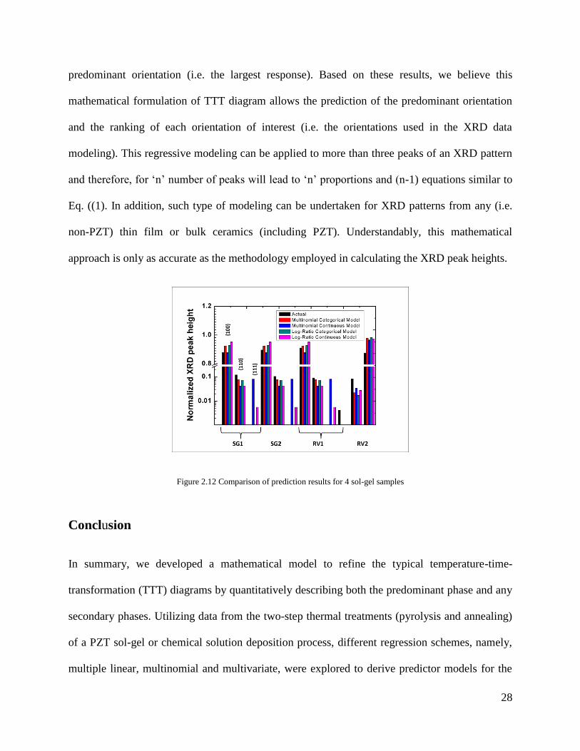
28
predominant orientation (i.e. the largest response). Based on these results, we believe this
mathematical formulation of TTT diagram allows the prediction of the predominant orientation
and the ranking of each orientation of interest (i.e. the orientations used in the XRD data
modeling). This regressive modeling can be applied to more than three peaks of an XRD pattern
and therefore, for ‘n’ number of peaks will lead to ‘n’ proportions and (n-1) equations similar to
Eq. ((1). In addition, such type of modeling can be undertaken for XRD patterns from any (i.e.
non-PZT) thin film or bulk ceramics (including PZT). Understandably, this mathematical
approach is only as accurate as the methodology employed in calculating the XRD peak heights.
Figure 2.12 Comparison of prediction results for 4 sol-gel samples
Conclusion
In summary, we developed a mathematical model to refine the typical temperature-time-
transformation (TTT) diagrams by quantitatively describing both the predominant phase and any
secondary phases. Utilizing data from the two-step thermal treatments (pyrolysis and annealing)
of a PZT sol-gel or chemical solution deposition process, different regression schemes, namely,
multiple linear, multinomial and multivariate, were explored to derive predictor models for the

29
level of (100), (110) and (111) crystallinity in a thin film sample. The best validation of
experimental data was obtained with multinomial regression. We have demonstrated the
simplicity and efficacy of this methodology for every day laboratory use and expect extendibility
to non thin film systems. In doing so, we have also taken out some of the specificity, like
operator induced variability, that is usually observed in such experimentation.
References
[1] Kuwata J, Uchino K, Nomura S. Phase transitions in the Pb (Zn1/3Nb2/3) O3-PbTiO3
system. Ferroelectrics 1981;37:579.
[2] Kuwata J, Uchino K, Nomura S. Dielectric and piezoelectric properties of 0.91 Pb
(Zn1/3Nb2/3) O3-0.09 PbTiO3 single crystals. Japanese journal of applied physics
1982;21:1298.
[3] Park S-E, Shrout TR. Ultrahigh strain and piezoelectric behavior in relaxor based
ferroelectric single crystals. Journal of applied physics 1997;82:1804.
[4] Park S-E, Shrout TR. Characteristics of relaxor-based piezoelectric single crystals for
ultrasonic transducers. IEEE transactions on ultrasonics, ferroelectrics, and frequency control
1997;44:1140.
[5] Fu H, Cohen RE. Polarization rotation mechanism for ultrahigh electromechanical
response in single-crystal piezoelectrics. Nature (London) 2000;403:281.
[6] Du X-h, Zheng J, Belegundu U, Uchino K. Crystal orientation dependence of
piezoelectric properties of lead zirconate titanate near the morphotropic phase boundary. Applied
physics letters 1998;72:2421.
[7] Norga GJ, Fe L. Orientation selection in Sol-gel derived PZT thin films. Mat. Res. Soc.
Symp. Proc. 2001;655:CC9.1.1.
[8] Chen S-Y, Chen I-W. Temperature-Time Texture Transition of Pb(Zr(1-x)Ti(x))O3 Thin
Films: II, Heat Treatment and Compositional Effects. Journal of American Ceramic Society
1994;77:2337.
[9] Chen S-Y, Chen I-W. Temperature-Time Texture Transition of Pb(Zr(1-x)Ti(x))O3 Thin
Films: I, Role of Pb-rich Intermediate Phases. Journal of American Ceramic Society
1994;77:2332.
[10] Huang Z, Zhang Q, Whatmore RW. The rolo of an intermetallic phase on the
crystallization of lead zirconate titanate in sol-gel process. Journal of Materials Science Letters
1998;17:1157.
[11] Park CS, Kim SW, Park GT, Choi JJ, Kim HE. Orientation control of lead zirconate
titanate film by combination of sol-gel and sputtering deposition. Journal of materials research
2005;20:243.
[12] Agresti A. Categorical Data Analysis: Wiley-Interscience, 2002.
[13] Aitchison J. The Statistical Analysis of Compositional Data (Monographs on Statistics
and Applied Probability): Springer, 1986.

30
Chapter 3
Ellipsometric Characterization of Multi-component Thin
Films: Determination of Elemental Content from Optical
Dispersion
Ronnie Varghese,1*
Greg Pribil,2 W. T. Reynolds Jr,
3 and Shashank Priya
1
1Center for Energy Harvesting Materials and Systems (CEHMS), Bio-Inspired Materials and Devices Laboratory (BMDL), Virginia Tech, Blacksburg, VA 24061, USA
2J.A. Woollam. Co. Inc, Lincoln, NE 68508, USA 3Materials Science and Engineering Department, Virginia Tech, Blacksburg, VA 24061, USA
Abstract
This paper provides the correlation between the composition of a given thin film to its optical
dispersion properties. Gladstone-Dale (G-D) relationships have been used in optical mineralogy
to relate density of crystalline compounds to their average refractive index. We purport to use a
‘reverse’ G-D approach and determine the composition of multi-component thin films from their
optical properties. As a model system, we focus on complex perovskite ferroelectric thin film
and apply the derived relationships to determine the stoichiometry. The wavelength dispersion of
refractive index and extinction coefficient of various Pb(Zr,Ti)O3 (PZT) thin films was
measured using Variable Angle Spectroscopic Ellipsometry (VASE). Elemental compositions
were measured using Energy Dispersive X-ray analysis (EDX) and Electron Probe Micro
Analysis (EPMA). Wemple-DiDomenico, Jackson-Amer, Tauc and Urbach optical relationships
and related parameters were used to extract correlations to elemental content. Both theoretical
and semi-empirical approaches to calculate the electronic polarizability of PZT were employed

31
and their variation with elemental content was computed. Perovskite tolerance and octahedral
factors were also analyzed against the optical and polarizability parameters. Lastly, these factors
and relationships were combined to realize a model for predicting the elemental content of a thin
film system.
Keywords: Thin films; Optical properties; Refractive index; Optical dispersion; Absorption
coefficient
Introduction
Many attempts have been made to empirically or theoretically derive the correlation between
optical absorption, mass density and electronic properties of materials. Gladstone and Dale[1]
(G-D) provided the empirical correlation between the average index of refraction ‘n’ and mass
density m of a mixture as:
1i i
im
nk w
(1)
where ik is the refractive coefficient and iw is the weight fraction of component ‘i’ making up the
solution. The common applications of G-D relationships are: (l) the calculation of the refractive
index ‘n’ from measured density and the specific refractive energy derived from the chemical
analysis; and (2) the calculation of density from the mean refractive index and the specific
refractive energy. Specific refractive energy refers to the refractive index of any substance minus
unity, divided by the density. The G-D relationship defines the optical properties of a solid
solution as the sum of the optical properties of its comprising oxides. An analogous relationship
is the Beer-Lambert’s law which is used to describe the relationship between light absorption and
the concentration of an irradiated sample. One drawback of the G-D relationship is that the
32
refractive coefficients are empirically derived for a certain optical spectrum or line. In many
cases, the relationship is only valid for n > 1.4[2],[3]. Also in the G-D relation, specific
refractivity of each component assumes unrealistically that the effect of each component is
separate and independent of the others.
To illustrate, on applying the G-D relationship to Pb1.1(Zr0.52Ti0.48O3) (PZT) thin film and
using the refractive coefficients for the constituent oxides derived by Larsen[4] with the
stoichiometry and molecular weights we get:
2 2
2 2 2 2
1 0.15 0.20
PbO PbO ZrO ZrO
m PbO PbO ZrO ZrO TiO TiO
n mw mole fraction mw mole fraction
mw mole fraction mw mole fraction mw mole fraction
2 2
2 2 2 2
0.40
TiO TiO
PbO PbO ZrO ZrO TiO TiO
mw mole fraction
mw mole fraction mw mole fraction mw mole fraction
(2)
For PZT,ρm~7.8gm/cc and so, n=2.457. From the above equation, we realize that by
changing the stoichiometry or the concentration one can alter the average refractive index.
Conversely, as seen from the above equation, the change in average refractive index will not
uniquely identify a particular concentration. Inspired by the literature on the G-D relationship,
we decided to investigate the possibility of developing a reverse relationship whereby optical
properties could be used to determine the composition. Particularly, can the optical properties of
a solid solution provide a measure of the concentration or composition of its constituents in
complex oxides?
To illustrate the approach, we selected PZT due to its huge industrial relevance. PZT films have
been studied for ferroelectric random access memory that can provide nonvolatile memory
operation with fast writing time while reducing the power requirement. PZT films are also being
pursued as gate dielectric in ferroelectric memory field-effect transistor providing a
33
nondestructive readout operation with high density. La-modified PZT films are candidate
materials for the electro-optic modulators and light activated actuators. Further, doped PZT films
near morphotropic phase boundary form the part of vast number of actuation and sensing
devices.
Teertstra[5] invoked Newtonian particle theory of light to explain the G-D relationship
and postulated that incident light (as a particle) is affected by inter-atomic bonding (i.e. non-
linear path through material). He proposed a new coefficient, ‘specific ionic refractivity’, which
is characteristic of each elemental ion in a material. For each atom at a particular crystallographic
site, this coefficient can be calculated from the physical properties of its ion in the structure [5-
7]. For a specific structural formula of a crystalline material, Teertstra[7] suggested that the
weight fraction of its components can be determined by iteration from the calculated (from
existing empirical data of similar compounds) ionic G-D coefficients of the constituent elements,
measured average refractive index and unit cell parameters from crystallographic data (i.e. a-
priori knowledge of site occupancies; not possible for amorphous or polycrystalline material).
The values derived under so many constraints must also meet the boundary condition of
measured density and be valid across a wide incident wavelength range. These ionic coefficients
cannot be assumed to remain constant in different compounds – for example, Pb2+
coefficients
will be different in PbTiO3 vs. PbZrO3. Multivalent states of the same ion will present challenges
in analysis as the substitution may not be site specific.
In contrast, we utilized the dielectric polarization effect of an electromagnetic light wave
traversing a medium. The optical dispersion (i.e. the variation of refractive index and extinction
coefficient with incident light wavelength or energy) of a material is inherently related to its
concentration, valency or coordination of its constituents, band tails and gap states. An increase
34
in refractive index can occur by the increase in ionic charge or valency, increased atomic number
or decreased atomic or ionic radii of a cation and covalently bonded anion[5]. Therefore, we can
expect that a variation in elemental composition will affect the broad spectrum (including optical
energies > band gap) of an analyte[8]. The models thus developed can be used to predict the
composition of a multi-component compound irrespective of its level of crystallinity.
Experimental Details
Material Characterization
Unlike DC sputtering of conductive films, non-conductive PZT films require RF power sources
for plasma generation. Pb1.1(ZrxTi1-x)O3 target for x = 0.52 with 10% excess Pb to compensate for
Pb loss during post deposition annealing, was prepared by mixed oxide method. RF sputtering
plasma deposition (Figure 3.1(a)) involves Argon ion bombardment on the PZT target and
subsequent deposition of the sputtered PZT material onto a grounded or biased substrate. The
sputter target concentrations based on the stoichiometry were Pb at 21.57%, Zr at 10.20%, Ti at
9.41% and O at 58.82%. On the Aja International (Scituate, MA, USA) RF sputtering system,
the process variables were argon and oxygen flows, chamber pressure, RF power (DC Bias),
working distance, temperature, rotation speed and substrate bias. The deposition time was fixed
at 30 minutes. RF sputter deposition operating space was explored using statistical Design of
Experiments (DOE using DesignExpert™ software) and trends and ANOVA (Analysis of
Variance) models were formulated. After measurement of the dispersion of refractive index and
extinction coefficient using Variable Angle Spectroscopic Ellipsometry (VASE), the
composition of these films was measured using either Energy Dispersive X-ray analysis (EDX)
or Electron Probe Micro Analysis (EPMA) or both. In the first screening experiment (Figure
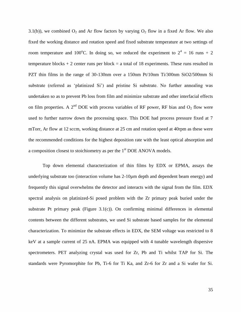
35
3.1(b)), we combined O2 and Ar flow factors by varying O2 flow in a fixed Ar flow. We also
fixed the working distance and rotation speed and fixed substrate temperature at two settings of
room temperature and 100oC. In doing so, we reduced the experiment to 2
4 = 16 runs + 2
temperature blocks + 2 center runs per block = a total of 18 experiments. These runs resulted in
PZT thin films in the range of 30-130nm over a 150nm Pt/10nm Ti/300nm SiO2/500mm Si
substrate (referred as ‘platinized Si’) and pristine Si substrate. No further annealing was
undertaken so as to prevent Pb loss from film and minimize substrate and other interfacial effects
on film properties. A 2nd
DOE with process variables of RF power, RF bias and O2 flow were
used to further narrow down the processing space. This DOE had process pressure fixed at 7
mTorr, Ar flow at 12 sccm, working distance at 25 cm and rotation speed at 40rpm as these were
the recommended conditions for the highest deposition rate with the least optical absorption and
a composition closest to stoichiometry as per the 1st DOE ANOVA models.
Top down elemental characterization of thin films by EDX or EPMA, assays the
underlying substrate too (interaction volume has 2-10µm depth and dependent beam energy) and
frequently this signal overwhelms the detector and interacts with the signal from the film. EDX
spectral analysis on platinized-Si posed problem with the Zr primary peak buried under the
substrate Pt primary peak (Figure 3.1(c)). On confirming minimal differences in elemental
contents between the different substrates, we used Si substrate based samples for the elemental
characterization. To minimize the substrate effects in EDX, the SEM voltage was restricted to 8
keV at a sample current of 25 nA. EPMA was equipped with 4 tunable wavelength dispersive
spectrometers. PET analyzing crystal was used for Zr, Pb and Ti whilst TAP for Si. The
standards were Pyromorphite for Pb, Ti-6 for Ti Ka, and Zr-6 for Zr and a Si wafer for Si.
36
Interestingly, Ti and Zr concentrations were found to be linearly correlated which could be
attributed to their equivalent sputtering yields.
Figure 3.1 (a) RF sputter configuration for PZT thin films, (b) PZT RF Sputter process variables, and (c) EDX of PZT on
platinized Si – on zooming in, Zr peak is buried under Pt peak
As deposited PZT RF thin films were mostly amorphous - which is expected as the
crystallization temperature is generally above 600oC (confirmed by X-ray diffraction).
Optical Characterization
Optical measurements were performed on a J.A.Woollam VASE in rotating analyzer mode in the
wavelength range of 300-800nm (4.13-1.55eV) at incidence angles of 65˚, 70˚ and 75˚.
Ellipsometry measures two values Ψ and ∆ that expresses the amplitude ratio and phase
difference between the ‘s’ and ‘p’ polarizations of the reflected light from the sample. A general
oscillator layer (hereafter, referred to as ‘Genosc’) model was employed to fit the ellipsometric
data of each as-deposited thin film. The Genosc layer models the dielectric function of the PZT
thin film as a linear summation of the real and complex oscillators (each a function of
wavelength or photon energy)[9]. The PZT Genosc included a summation of two Gaussian
oscillators and an offset to the real part of the dielectric function :

37
1 2 Offset Gaussians E, A1, E1, B1 Gaussians (E, A2, E2, B2)E E i E (3)
For a Gaussian Oscillator model[9], the above equation simplifies to the Gaussians terms for 2
with a Kramer-Kronig consistent profile for 1 .
2 2
2 where
n nE E E E
n nE A e A e
2 ln 2
nB (4)
The fit parameters for the ‘n’th Gaussian Oscillator are amplitude (An), center energy (En) and
broadening (Bn) of the absorption peak. Bn equals the Full Width-Half-Maximum (FWHM)
value of the Gaussian curve.
The constitutive relationships relating dielectric polarization and optical properties with respect
to energy or wavelength are reproduced here from reference [10].The complex dielectric
function is given as –
1 2 E E i E hc
where E
2 2
1 n k ; 2 2nk ; 4 ;a k
*
1 2 n n ik i (5)
The Kramer Kronig relationship link ‘n’ and ‘k’ (and therefore, ε1 and ε2) as:
' '
2 2
0
2 ( )1 ' ;
'
E k En dE
E E
'2 2
0
12'
'
n Ek dE
E E
(6)
The optical band gap Eg of amorphous PZT thin films can be considered as a direct band gap
transition between the valence band and the conduction band states (these states can include the
band tails created by localized states at the absorption edge)[8]. The Tauc Gap Eg of amorphous

38
materials is derived from the following relationships between ε2 and ‘a’ absorption coefficient
vs. photon energy[11, 12].
2
2 2 ;
g
Tauc
E EB
E
1/2
Tauc ga B E E (7)
BTauc is inversely related to refractive index. For direct band gap material, the optical band gap,
Eg, is derived from the intercept on the x-axis of a tangent line from the curve generated by
square of ‘aE’ vs. photon energy ‘E’ (often referred to as the Tauc plot; for indirect band gap
material, the square root of ‘aE’ is used).
2( ) gaE E E (8)
Below this power law region of Tauc plot, there is an exponential region where the Urbach
rule[11] applies and this area accounts for band tails or the localized states in the band gap. The
inverse slope, Urbach width, Eu, determined from log(a) vs. photon energy plot is a measure of
the disorder of the system producing the absorption tail in the Tauc plot.
/
0uE E
a a e (9)
In the sub-gap region, as per Jackson and Amer[13], the area under the absorption ‘a’ vs. photon
energy ‘E’ curve, is proportional to the localized defect states in the band gap. This proportional
parameter is ‘as-g’ and is given as:
gsub E
s g o
E
a a dE
(10)

39
In materials with a band gap, the refractive index at energies below the band gap is correlated to
the absorption above the band gap as per the following version of the Kramer-Kronig
relationship ( denotes the principal part)[14].
' '2
2 2
2 ( )1 '
'gE
E k En dE
E E
(11)
Below the band gap the relationship evolves into the Wemple-DiDomenico dispersion model for
refractive index given as:
2
2 21 d o
o
E En
E E
(12)
where Ed is the dispersion energy and is a measure of the optical transitions below the band gap
and affected by the structural order of the material. Whilst Eo is the single oscillator energy that
is correlated with the band gap and peak of the imaginary part of the complex permittivity or
refractive index. These two parameters can be estimated from the plot of 1/(n2-1) vs. E
2. Ed , is
empirically found to be dependent on coordination number of the cation Nc , chemical valency of
the anion Za, the effective number of valence electrons per anion Ne and finally β which has the
value 0.26 +/-0.04 eV for ionic and 0.37 +/- 0.05 eV for covalent bonded atoms in the material.
d c a eE N Z N (13)
Results
Due to the variation in optical constants across the large number of samples (and process
conditions), not all samples required the use of all the fit parameters (A1, B1, E1, A2, B2, E2 for
2 Gaussians and an e1 offset) of Equation 3. For some samples, 2 Gaussian oscillators were

40
required to describe the n & k dispersion. The 2nd Gaussian was less important for samples with
simpler dispersions (in which case there would be more inter-correlation between the parameters
of the 2 Gaussians due to the less flexibility necessary to fit a simpler dispersion shape). The
challenge occurs when multiple oscillators are employed to describe the overall (particularly
broad) dispersion shape, there will likely be some internal correlation between the parameters.
To avoid such concerns, our goal was to use the oscillator(s) to determine the final overall n & k
dispersion shape and that this dispersion shape could be described by using different general
dispersion models which are available to the researcher. In our case, 2 Gaussians were used, but
the overall basic shape could likely be obtained by using combinations of multiple oscillators –
say, multiple Gaussian, Lorentz, or Tauc-Lorentz, etc. So once an optical model is used to
determine the overall n & k dispersion, then we followed up with other relationships (Tauc,
Urbach, Jackson-Amer, Wemple DiDomenico, etc) to extract parameters specific to this overall
shape. These relationships were based off spectroscopic data and therefore, are expected to show
correlation to film composition. The details of 1st DOE are shown in table below. We did not get
any visible deposition for 2 runs. The significant factors (labeled; out of the 2n-1 combinations of
the 4 factors) were easily decipherable as shown in the Half Normal Probability plots (Figure
below). The design, resultant responses and significant factors of the 2nd
DOE are shown in
Table 3.2 and Figure 3.3 below. Uncertainty Figure of Merit (FOM)[9] of n & k was calculated
using Monte Carlo Fit-Result Analysis to be ±0.000212748 and ±6.58962E-05 respectively or
±0.010% and ±0.256% of average n and k. The uncertainty is calculated as FOM(n) and FOM(k)
where the FOM is product of the standard 90% confidence limit and the square root of the Mean
Square Error (MSE), a weighted Chi-square estimate of measurement error.

41
Table 3.1 1st Full Factorial Statistical Design of Experiment in 4 process variables and the measured VASE responses
Ru
n
Bloc
k
Factor 1 Factor 2 Factor 3 Factor 4 Thickness
(A)
n@633n
m
k@633n
m
A:O2 :Ar
ratio
B:Pressur
e
C:RF
Power
D:RF1
bias
sccm mT W W
1 100C 0.25 7 200 0 672.66 1.9781 0.0044
2 100C 0.25 3 200 10 320.77 2.1745 0.0232
3 100C 0 3 200 0 1297.76 2.2848 0.0066
4 100C 0 3 100 10 312.11 2.3674 0.0259
5 100C 0 7 200 10 561.92 2.1993 0.0014
6 100C 0 7 100 0 666.47 2.2757 0.3482
7 100C 0.5 5 150 5 270.01 2.0949 0.0263
8 100C 0.25 3 100 0 347.19 2.1596 0.0841
9 100C 0.25 7 100 10
10 25C 0.5 5 150 5 342.77 2.2178 0.0140
11 25C 0.25 7 200 10 363.15 2.267 0.0122
12 25C 0.25 7 100 0 264.13 2.1342 0.0096
13 25C 0.25 3 200 0 827.52 2.2697 0.0243
14 25C 0 7 100 10 281.59 2.1595 0.0026
15 25C 0.25 3 100 10
16 25C 0 3 200 10 663.79 2.2118 0.0082
17 25C 0 7 200 0 1280.71 2.2647 0.0125
18 25C 0 3 100 0 564.84 2.5352 0.5790

42
Figure 3.2 Half Normal Probability plots of VASE responses – Thickness, refractive index ‘n’ and extinction coefficient ‘k’ for
the 1st DOE
Table 3.2 2nd Full Factorial Statistical Design of Experiment in 3 process variables and the measured VASE responses
Run Factor 1 Factor 2 Factor 3 Thickness (A) n@633nm k@633nm
A:O2 flow B:RF Power C:RF1 Bias
sccm mT W
1 0 200 0 1186.47 2.3377 0.0060
2 0 200 2 969.42 2.3772 0.0000
3 2 200 2 492.52 2.2235 0.0048
4 0 150 0 822.34 2.3109 0.0066
5 2 150 2 257.9 2.2001 0.0035
6 1 175 1 476.87 2.3204 0.0161
7 2 150 0 348.7 2.1702 0.0149
8 2 200 0 613.42 2.2253 0.0175
9 0 150 2 648.55 2.2580 0.0027
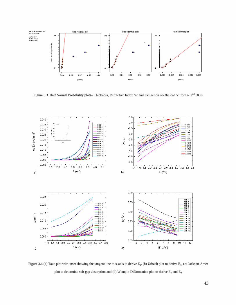
43
Figure 3.3 Half Normal Probability plots– Thickness, Refractive Index ‘n’ and Extinction coefficient ‘k’ for the 2nd DOE
Figure 3.4 (a) Tauc plot with inset showing the tangent line to x-axis to derive Eg, (b) Urbach plot to derive Eu, (c) Jackson-Amer
plot to determine sub-gap absorption and (d) Wemple-DiDomenico plot to derive Eo and Ed
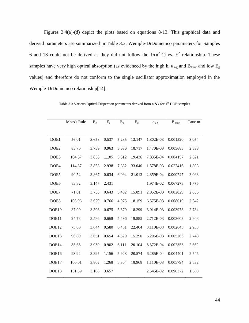
44
Figures 3.4(a)-(d) depict the plots based on equations 8-13. This graphical data and
derived parameters are summarized in Table 3.3. Wemple-DiDomenico parameters for Samples
6 and 18 could not be derived as they did not follow the 1/(n2-1) vs. E
2 relationship. These
samples have very high optical absorption (as evidenced by the high k, αs-g and BTauc and low Eg
values) and therefore do not conform to the single oscillator approximation employed in the
Wemple-DiDomenico relationship[14].
Table 3.3 Various Optical Dispersion parameters derived from n &k for 1st DOE samples
Moss's Rule Eg
Eu
Eo Ed αs-g BTauc Tauc m
DOE1 56.01 3.658 0.537 5.235 13.147 1.802E-03 0.001520 3.054
DOE2 85.70 3.759 0.963 5.636 18.717 1.470E-03 0.005685 2.538
DOE3 104.57 3.838 1.185 5.312 19.426 7.835E-04 0.004157 2.621
DOE4 114.87 3.853 2.938 7.882 33.040 1.578E-03 0.022416 1.808
DOE5 90.52 3.867 0.634 6.094 21.012 2.859E-04 0.000747 3.093
DOE6 83.32 3.147 2.431 1.974E-02 0.067273 1.775
DOE7 71.81 3.738 0.643 5.402 15.891 2.052E-03 0.002829 2.856
DOE8 103.96 3.629 0.766 4.975 18.159 6.575E-03 0.008019 2.642
DOE10 87.00 3.593 0.675 5.379 18.299 3.014E-03 0.003978 2.784
DOE11 94.78 3.586 0.668 5.496 19.885 2.712E-03 0.003603 2.808
DOE12 75.60 3.644 0.580 6.451 22.464 3.110E-03 0.002645 2.933
DOE13 96.89 3.651 0.654 4.529 15.290 5.206E-03 0.005263 2.748
DOE14 85.65 3.939 0.902 6.111 20.104 3.372E-04 0.002353 2.662
DOE16 93.22 3.895 1.156 5.928 20.574 6.285E-04 0.004401 2.545
DOE17 100.01 3.802 1.268 5.304 18.968 1.110E-03 0.005794 2.532
DOE18 131.39 3.168 3.657 2.545E-02 0.098372 1.568

45
Wemple-DiDomenico parameters show correlation to elemental content - similar to that
observed for epitaxial, crystalline and stoichiometric PZT thin films[15]. However, in our 1st
DOE films the Zr and Ti contents are directly correlated and Pb and O contents inversely
correlated to Eg, Eo and Ed. Also, the refractive index is inversely correlated to Eo and not
correlated to Ed. Please note that Eo is correlated to band gap Eg whilst Ed is the average strength
of interband optical transitions and is affected by the structural order of the material[14]. In the
1st DOE, the stoichiometry ratio Pb/(Ti+Zr) varies from 0.28-2.24 whilst Zr/Ti varies 0.13-0.86
(<1.083 for PZT 52/48). The refractive index increases with both Ti and Zr concentration and
only slightly with Pb.
Figure 3.5 Scatterplot of Tauc Optical Gap Eg and Wemple-DiDomenico parameters Eo and Ed vs. Atomic fractions
For the 2nd
DOE, the various optical parameters were derived from n & k data (Table
3.4). Both Eo and Ed show good dependence on elemental content with the latter being the best.
O, Zr and Ti content were more correlated than Pb. We attribute the better correlations to the
tighter distribution of relative atomic contents of Pb, Zr vs. Ti. The Pb/(Zr+Ti) for all 2nd
DOE
samples are > 1 (1.23-2.13) and Zr/Ti ratio ranges from 0.6-1.8 (ideal = 1.083).
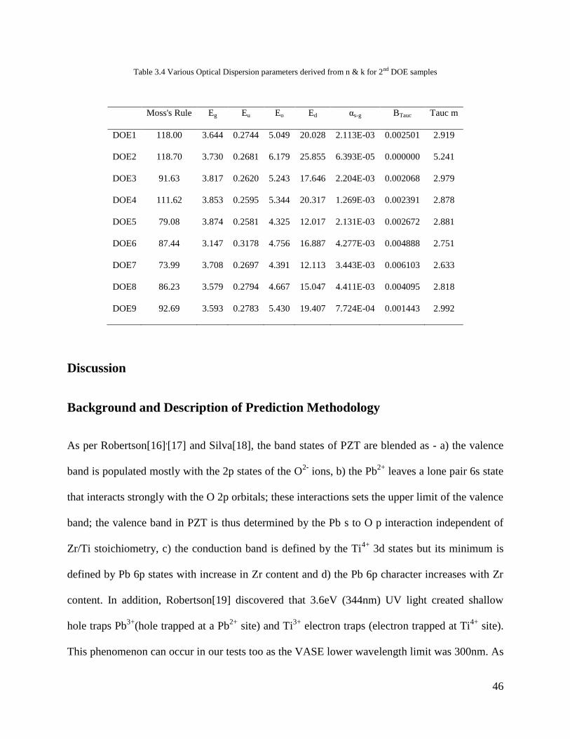
46
Table 3.4 Various Optical Dispersion parameters derived from n & k for 2nd DOE samples
Moss's Rule Eg Eu Eo Ed αs-g BTauc Tauc m
DOE1 118.00 3.644 0.2744 5.049 20.028 2.113E-03 0.002501 2.919
DOE2 118.70 3.730 0.2681 6.179 25.855 6.393E-05 0.000000 5.241
DOE3 91.63 3.817 0.2620 5.243 17.646 2.204E-03 0.002068 2.979
DOE4 111.62 3.853 0.2595 5.344 20.317 1.269E-03 0.002391 2.878
DOE5 79.08 3.874 0.2581 4.325 12.017 2.131E-03 0.002672 2.881
DOE6 87.44 3.147 0.3178 4.756 16.887 4.277E-03 0.004888 2.751
DOE7 73.99 3.708 0.2697 4.391 12.113 3.443E-03 0.006103 2.633
DOE8 86.23 3.579 0.2794 4.667 15.047 4.411E-03 0.004095 2.818
DOE9 92.69 3.593 0.2783 5.430 19.407 7.724E-04 0.001443 2.992
Discussion
Background and Description of Prediction Methodology
As per Robertson[16],[17] and Silva[18], the band states of PZT are blended as - a) the valence
band is populated mostly with the 2p states of the O2-
ions, b) the Pb2+
leaves a lone pair 6s state
that interacts strongly with the O 2p orbitals; these interactions sets the upper limit of the valence
band; the valence band in PZT is thus determined by the Pb s to O p interaction independent of
Zr/Ti stoichiometry, c) the conduction band is defined by the Ti4+
3d states but its minimum is
defined by Pb 6p states with increase in Zr content and d) the Pb 6p character increases with Zr
content. In addition, Robertson[19] discovered that 3.6eV (344nm) UV light created shallow
hole traps Pb3+
(hole trapped at a Pb2+
site) and Ti3+
electron traps (electron trapped at Ti4+
site).
This phenomenon can occur in our tests too as the VASE lower wavelength limit was 300nm. As

47
per Silva[18], the Pb to Zr-O6 or Ti-O6 bonding is ionic whilst that between Zr-O and Ti-O, the
bonds are covalent. Silva confirmed with Density Functional Theory (DFT) modeling that any
displacement by Ti or Zr will cause a decrease in Eg (by enlargement of the valence and
conduction bands) and the creation of gap states. Therefore, both the bonding state of the Pb, Zr
and Ti with O and their relative atomic positions can affect the optical band gap. For both
DOE’s, Jackson Amer parameter, as-g is affected slightly by elemental content – an exponential
increase with Pb content and decreasing exponential with O, Zr and Ti contents. Less oxygen
vacancies can be expected to decrease localized defect states. According to Davis and Mott[20],
the presence of high density of localized states in the band structure is responsible for lower
values of the optical gap. We confirm that with the inverse relationship noticed between Jackson
Amer parameter as-g and optical band gap Eg. As per Watanabe[21], the refractive index and the
square of the slope of the Tauc plot (known as B-parameter or BTauc) are inversely proportional
to the width of the tail states and is a measure of the gradient of the density of states at the
conduction band edge. The lower the product of the two, sharper is the conduction band edge.
We observed a consistent correlation between n*BTauc2 and band edge sharpness parameters,
Urbach energy, Eu, and Jackson Amer parameter as-g. Moss’s rule[22] states that n4Eg is a
constant (~95eV; slope in a plot of n4 vs. 1/Eg). For our films, the Moss’s parameter ranges from
56-131 eV independent of elemental composition. Tauc optical gap, Eg, and Wemple-
DiDomenico parameters, Eo and Ed, show compositional dependencies (Figure 3.5). These mixed
results can be attributed to the fact that none of the prior optical theories (summarized in Table
3.5) provide a constitutive optical relationship that captures the effect of relative concentrations
of elements in the material. Next, we reveal this missing link.

48
Table 3.5 Summary of Optical parameters derived from Ellipsometric data
Type of Plot Calculated Parameter Nomenclature Computation
Tauc Optical Band Gap Eg Intercept on x-axis of tangent line from (aE)2
vs photon Energy (E)
Urbach Urbach Width Eu Inverse slope of log of absorption ‘a’ vs.
photon energy (E) where E < Eg
Jackson-Amer Sub-gap absorption as-g Area under absorption ‘a’ vs. photon energy
(E) where E < Eg
Wemple-
DiDomenico
Dispersion energy and Single
Oscillator energy
Ed and Eo Computed from plot of 1/(n2-1) vs E
2 using
Eq. 12
Electronic and ionic polarizations are due to field induced dipole moments while
orientational polarization is due to permanent dipole moments. These three are categorized as
paraelectric polarization. There are 3 non-paraelectric polarizations – a) ferroelectric or
spontaneous (non-centrosymmetric materials), b) space charge (due to trapped charges from
mobile ions or charge carrier traps in amorphous material) and c) hopping (due to localized states
in glasses and amorphous semiconductors). From these definitions[23], as deposited RF
sputtered PZT films may have paraelectric along with space charge and hopping polarizations.
For multi-component absorbing films, like our amorphous PZT films, we need to expand beyond
the above simple correlations. For this purpose, we will utilize the relationship between
microscopic polarizability and macroscopic refractive index – the Lorentz-Lorenz equation [24]:
, , m m r m ii
22 2 2 2
, 22 2 2
( 1)( 2) 2 3
4( 2) 2m r
A
n k n k nk M
Nn k nk

49
2 2 2 2 2
2 2 2 2
( 1)( 2) (2 )
( 2) (2 )real
n k n k nkIf LL
n k nk
,
3,
4m r real
A
Mthen LL
N
, 2 2 2 2
6 3
4( 2) (2 )m i
A
nk M
Nn k nk
(14)
The imaginary part of electronic polarizability is often a few orders of magnitude less than the
real part. The above relationship also provides a method to measure the density of a sample
based on its optical properties and polarizability. An empirical relationship for electronic
polarizability has also been derived by Reddy et.al.[25] using band gap, Eg , and optical
electronegativity of the material, Δχ.
24 4.0270.395 ln (ln 4.564)and Δ 0.2688
7.027rrr g
K Me where K E
K
(15)
Optical electronegativity of a material is indicative of the nature of bonding and is a measure of
the strength of its ionicity and conversely, the lower it is, the higher the covalency. We had
noticed that optical band gap Eg increases with Zr (consistent with reference [16]) and Ti content
and decreases with Pb. Therefore, Reddy polarizability relationship will be ideal in capturing
these dependencies.
If we apply volume mixing rules for density[26], ρi and atomic weights Mi, we get the
following relationships for effective density ρe and effective molecular weight Me vs. the volume
fraction, vi (related to the atomic or molar fraction, fi) -
;e i i
i
v
;i ii
e
i i
ii
vM
v
M
i i i i i i
i A i i
i
i i i i i i
i i ii A i i
N M N M f M
Nv
N M N M f M
N
(16)

50
Thus, with the above mixing rules, the electronic polarizability relationships can incorporate the
confounded effects of elemental composition. Using Eq. 16, effective density ρe and effective
molecular weight Me is computed for each sample and substituted in Eq. 14 and 15 to compute
αm,r and αrrr for each sample. The equivalent effective electronic polarizability[26] is given by
e i i
i
f where fi is atomic or molar fraction given as i
i
ii
Nf
N
. For effective polarizability,
electronic polarizabilities for Pb2+
, Zr4+
, Ti4+
and O2-
of 4.9, 0.37, 0.19 and 2.22 (x e-24
) are taken
from literature[27]. Naturally, in amorphous films, one can expect other valencies of these
constituent elements and therefore, αe does not depict actuality well. The magnitudes of
αm,r>αrrr>αe across all samples. Figure 3.6 depicts each of these polarizabilities plotted against
elemental content for the 1st DOE samples.
For perovskites ABO3, like PZT, a tolerance factor (tf) has been proposed as a measure of
perovskite structure formability. An additional factor called the octahedral factor (of) is
combined to further improve predictability[28].
and
2 ( )
A O
B O
r rtf
r r
B
O
rof
r (17)
To accommodate the atomic fractions in PZT, these factors were modified as follows,
and
2 ( )
Pb Pb O O
PZT
Zr Zr Ti Ti O O
f r f rtf
f r f r f r
Zr Zr Ti Ti
PZT
O O
f r f rof
f r
(18)
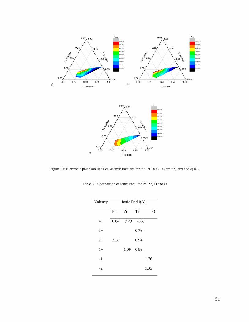
51
Figure 3.6 Electronic polarizabilities vs. Atomic fractions for the 1st DOE - a) αm,r b) αrrr and c) αe.
Table 3.6 Comparison of Ionic Radii for Pb, Zr, Ti and O
Valency Ionic Radii(A)
Pb Zr Ti O
4+ 0.84 0.79 0.68
3+ 0.76
2+ 1.20 0.94
1+ 1.09 0.96
-1 1.76
-2 1.32

52
The ionic radii[29] of Pb, Zr, Ti and O is given in the Table 3.6 (radii for perovskite PZT is in
italics). Therefore, for Pb(Zr0.52Ti0.48)O3, octahedral and tolerance factors can be calculated to be
0.186 and 0.777 respectively. We found that this group variable is highly correlated to
polarizability. Clearly, from Figure 3.5, Eo shows the best correlation to elemental content and
amongst the latter, Ti and Pb content is best correlated. Linear fits to Eo vs. elemental content
were made as listed below. The numbers in square brackets are Rsquared (R2) and Root Mean
Square error (RMSE) of the regressions (as computed by JMP™ statistical software). The
electronic polarizabilities are evidently correlated to each other as they all utilize atomic
fractions in their calculations.
2 0.132151 0.0375312* , [R 0.832, RMSE 0.009]Ti of E
0.066168 0.0193297* , [ 0.768, 0.006]Zr of E
0.3855925 0.0586112* , [ 0.857, 0.013]Pb of E
25 24 27 6.59 4.01 * , [ 0.999, 4.44e ]e e e tf
24 261 .821 0.452158* , [0.973,1 .22e ]rrr ee
24 26
, 1 .348 0.7085994* , [0.635, 8.63e ]m r ee (19)
For prediction, we substituted the empirically derived (from n&k dispersion data) LLreal, Eo and
Eg in the αm,r , αrrr and αe relationships and solved the above equations for the atomic fractions
with the added constraint that 1i
i
f .The results of the prediction methodology are shown in
Figure 3.7. The methodology has been summarized in the flow chart below (Figure 3.8).
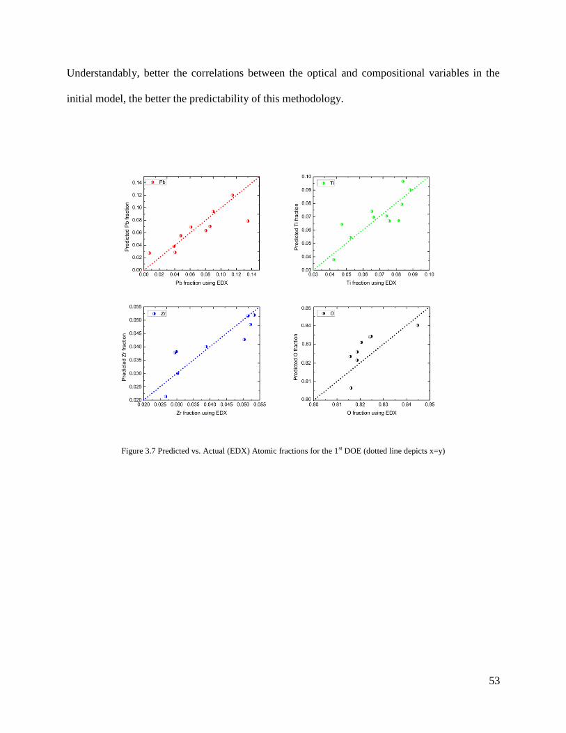
53
Understandably, better the correlations between the optical and compositional variables in the
initial model, the better the predictability of this methodology.
Figure 3.7 Predicted vs. Actual (EDX) Atomic fractions for the 1st DOE (dotted line depicts x=y)

54
Figure 3.8 Flowchart of Proposed methodology
Validation of Prediction Methodology
For validation, we utilized the data from the 2nd
DOE. The 2nd
DOE’s electronic
polarizability plots also demonstrated a tighter distribution amongst samples (Figure 3.9). For
prediction, from n&k dispersion data, we calculated 3 parameters LLreal, Ed and Eg for each
sample and substituted these values in their relationships in Equation 20 and solved these
equations for atomic fractions with the added constraint that 1i
i
f . The validation results show
good match (as noted by the narrow spread from the diagonal line x = y) to measured as shown
in Figure 3.10.

55
Figure 3.9 Electronic polarizabilities vs. Atomic fractions for the 2nd DOE - a) αm,r b) αrrr and c) αe
21 .0784887 0.0095597* , [ R 0.751, RMSE 0.020]O df E
0.00194 0.0008824* , [0.785, 0.002]Ti df E
0.026912 0.0027377* , [ 0.812, 0.019]Zr df E
25 24 27 2.61 3.508 * , [ 0.998, 2.41e ] e e e tf
25 26 9.96 1 .6814707* , [0.797, 4.34e ]rrr ee
24 26
, 5.73 3.7944908* , [0.825, 8.96e ]m r ee (20)

56
Figure 3.10 Predicted vs. Actual (EDX) Atomic fractions for the 2nd DOE (dotted line depicts x=y)
To quantify the effectiveness of this approach, in Table 3.7, we list the F-test and T-test
of the predicted vs. actual atomic fractions for each of the two DOE’s. F-test and T-test values >
5% (95% confidence interval) will prevent rejection of the null hypothesis for each pair (actual
vs. predicted) of elemental content data sets. The null hypothesis for F-test is that the variance is
equal between two samples and for T-test, the means of the two samples are statistically equal.
The F-test null hypothesis is rejected for the Oxygen content in the 1st DOE because the error in
predicted values of Oxygen is the sum of that for the other elements, Pb, Zr and Ti. Hence, better
the n-1 correlations between the elemental content and optical parameters, less the error in
prediction of the nth
elemental content.
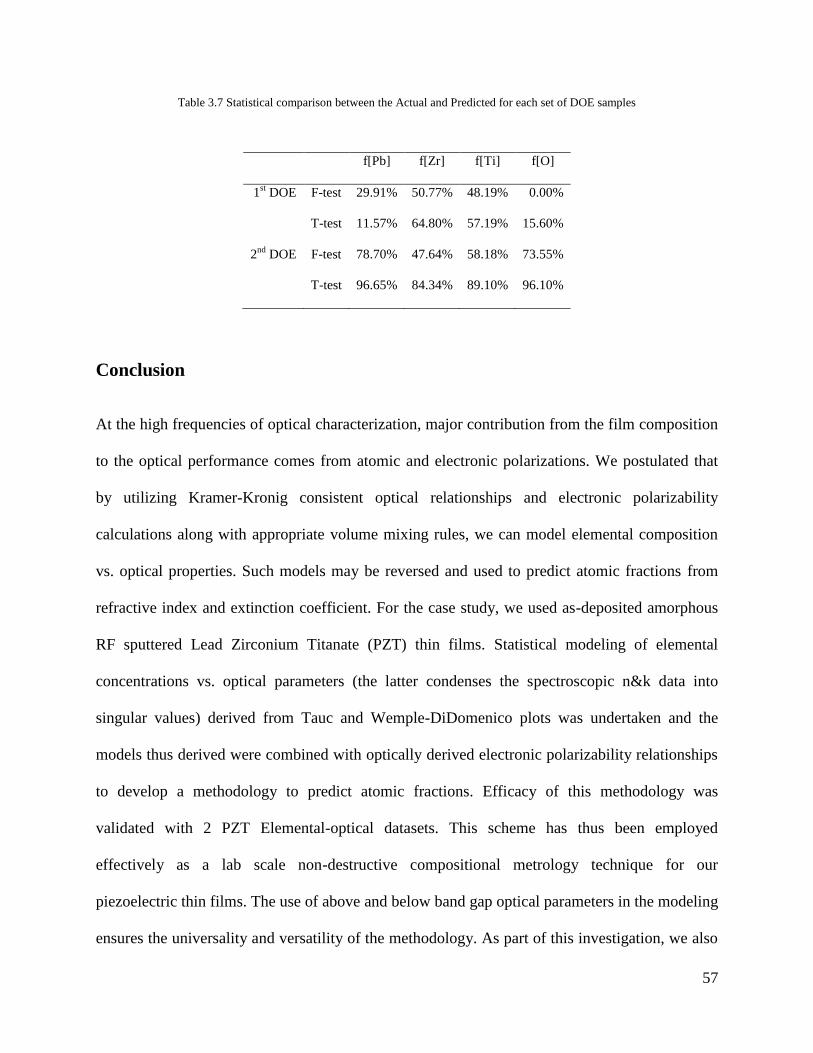
57
Table 3.7 Statistical comparison between the Actual and Predicted for each set of DOE samples
f[Pb] f[Zr] f[Ti] f[O]
1st DOE F-test 29.91% 50.77% 48.19% 0.00%
T-test 11.57% 64.80% 57.19% 15.60%
2nd
DOE F-test 78.70% 47.64% 58.18% 73.55%
T-test 96.65% 84.34% 89.10% 96.10%
Conclusion
At the high frequencies of optical characterization, major contribution from the film composition
to the optical performance comes from atomic and electronic polarizations. We postulated that
by utilizing Kramer-Kronig consistent optical relationships and electronic polarizability
calculations along with appropriate volume mixing rules, we can model elemental composition
vs. optical properties. Such models may be reversed and used to predict atomic fractions from
refractive index and extinction coefficient. For the case study, we used as-deposited amorphous
RF sputtered Lead Zirconium Titanate (PZT) thin films. Statistical modeling of elemental
concentrations vs. optical parameters (the latter condenses the spectroscopic n&k data into
singular values) derived from Tauc and Wemple-DiDomenico plots was undertaken and the
models thus derived were combined with optically derived electronic polarizability relationships
to develop a methodology to predict atomic fractions. Efficacy of this methodology was
validated with 2 PZT Elemental-optical datasets. This scheme has thus been employed
effectively as a lab scale non-destructive compositional metrology technique for our
piezoelectric thin films. The use of above and below band gap optical parameters in the modeling
ensures the universality and versatility of the methodology. As part of this investigation, we also
58
have noticed some interesting trends in the sub-gap density of states, optical band gap and
dispersion energy of PZT thin films.
Acknowledgements: The authors gratefully acknowledge the financial support from Air Force
Office of Scientific Research (AFOSR) through Young Investigator Program. We are also
greatly indebted to Clayton Loehn for the EPMA/WDS and EDX characterization work
conducted at Department of Geosciences at Virginia Tech and to Matthew Williams of
Department of Statistics at Virginia Tech for assistance with JMP™ statistical analysis.
References
[1] Gladstone JH. Researches on the refraction, dispersion, and sensitiveness of liquids.
Philosophical transactions of the Royal Society of London 1863;153:317.
[2] Eggleton RA. Gladstone-Dale constants for the major elements in silicates: Coordination
number, polarizability, and the Lorentz-Lorentz relation. Canadian Mineralogist 1991;29:525.
[3] Rocquefelte X. On the Volume-Dependence of the Index of Refraction from the
Viewpoint of the Complex Dielectric Function and the Kramers−Kronig Relation. The journal of
physical chemistry. B 2006;110:2511.
[4] Larsen ES. The microscopic determination of the nonopaque minerals: U.S. Geological
Survey Bulletin, 1921.
[5] Teertstra DK. THE OPTICAL ANALYSIS OF MINERALS. Canadian Mineralogist
2005;43:543.
[6] Teertstra DK. Index-of-refraction and unit-cell constraints on cation valence and pattern
of order in garnet-group minerals. Canadian Mineralogist 2006;44:341.
[7] Teertstra DK. Photon Refraction In Dielectric Crystals Using a Modified Gladstone-Dale
Relation. The Journal of Physical Chemistry C 2008;112:7757.
[8] Yang S, Mo D, Tang X. Spectroscopic ellipsometry studies of amorphous PZT thin films
with various Zr/Ti stoichiometries. Journal of Materials Science 2002;37:3841.
[9] Various. WVASE32 Manual. J.A. Woollam., Inc. .
[10] Fujiwara H. Spectroscopic Ellipsometry Principles and Applications: John Wiley & Sons,
2007.
[11] Capper P, Kasap S, Koughia C. Springer Handbook of Electronic and Photonic Materials.
Berlin: Springer US, 2006.
[12] Stenzel O. The Physics of Thin Film Optical Spectra: Springer, 2005.

59
[13] Jackson W, Amer N. Direct measurement of gap-state absorption in hydrogenated
amorphous silicon by photothermal deflection spectroscopy. Physical review. B, Condensed
matter 1982;25:5559.
[14] Wemple SH, DiDomenico M. Behavior of the Electronic Dielectric Constant in Covalent
and Ionic Materials. Physical review. B, Solid state 1971;3:1338.
[15] Moret MP, Devillers MAC, Worhoff K, Larsen PK. Optical properties of PbTiO[sub 3],
PbZr[sub x]Ti[sub 1−x]O[sub 3], and PbZrO[sub 3] films deposited by metalorganic chemical
vapor on SrTiO[sub 3]. Journal of Applied Physics 2002;92:468.
[16] Robertson J, Warren WL, Tuttle BA. Band states and shallow hole traps in Pb(Zr,Ti)O3
ferroelectrics. Journal of Applied Physics 1995;77:3975.
[17] Robertson J. Band structures and band offsets of high K dielectrics on Si. Applied
Surface Science 2002;190:2.
[18] Silva MS, Cilense M, Orhan E, Góes MS, Machado MAC, Santos LPS, Paiva-Santos CO,
Longo E, Varela JA, Zaghete MA, Pizani PS. The nature of the photoluminescence in
amorphized PZT. Journal of Luminescence 2005;111:205.
[19] Robertson J, Warren WL, Tuttle BA, Dimos D, Smyth DM. Shallow Pb3 hole traps in
lead zirconate titanate ferroelectrics. Applied Physics Letters 1993;63:1519.
[20] Davis EA, Mott NF. Conduction in non-crystalline systems V. Conductivity, optical
absorption and photoconductivity in amorphous semiconductors. Philosophical magazine
(London, England : 1945) 1970;22:0903.
[21] Watanabe T, Kazufumi A, Nakatani M, Suzuki K, Sonobe T, Shimada T. Chemical
Vapor Deposition of a-Si:H Films Utilizing a Microwave Excited Ar Plasma Stream. Japanese
journal of applied physics 1986;25:1805.
[22] Sahoo NK, Thakur, S., Tokas, R. B. Achieving superior band gap, refractive index and
morphology in composite oxide thin film systems violating the Moss rule. Journal of physics. D,
Applied physics 2006;39:2571.
[23] Kao KC. Dielectric Phenomena in Solids: Elsevier Academic Press, 2004.
[24] Khawaja EE, Bouamrane F, Al-Adel F, Hallak AB, Daous MA, Salim MA. Study of the
Lorentz-Lorenz law and the energy loss of 4He ions in titanium oxide films. Thin Solid Films
1994;240:121.
[25] Reddy RR, Nazeer Ahammed Y, Rama Gopal K, Abdul Azeem P, Sasikala Devi B, Rao
TVR, Behere SH. On the equivalence between Clausius–Mossotti and optical electronegativity
relations. Optical Materials 2003;22:7.
[26] Liu Y, Daum P. Relationship of refractive index to mass density and self-consistency of
mixing rules for multicomponent mixtures like ambient aerosols. Journal of aerosol science
2008;39:974.
[27] Tessman J, Kahn AH. Electronic Polarizabilities of Ions in Crystals. Physical review
1953;92:890.
[28] Li C, Soh KCK, Wu P. Formability of ABO3 perovskites. Journal of alloys and
compounds 2004;372:40.
[29] www.matweb.com.

60
Chapter 4
Thin Film Magnetostriction Measurement Using Laser
Doppler Vibrometry
Ronnie Varghese,1 Ravindranath Viswan,
2 Keyur Joshi,
1 Safoura Seifikar,
3 Yuan Zhou,
1 Justin Schwartz,
2
and Shashank Priya1,*
1Center for Energy Harvesting Materials and Systems (CEHMS), Bio-Inspired Materials and Devices Laboratory (BMDL), Virginia Tech,
Blacksburg, VA 24061, USA 2Materials Science and Engineering Department, Virginia Tech, Blacksburg, VA 24061, USA
3Department of Materials Science and Engineering, North Carolina State University, Raleigh, North Carolina 27695, USA
Abstract
This paper reports laser doppler vibrometry based measurement technique for the
magnetostriction in magnetic thin films. We have measured the strain induced by an AC
magnetic field in the polycrystalline cobalt ferrite and nickel ferrite thin films on silicon and
platinized silicon substrates under a DC magnetic bias. The experimental setup and the
derivation of the magnetostriction constant from the experimentally measured deflection are
discussed in detail. A comparative analysis was conducted with the Vibrating Sample
Magnetometer (VSM) measurement and the value derived from the bending theory calculations
of magnetically induced torque. At high DC magnetic field bias, the magnetization values
calculated from the measured magnetostriction values match with the actual magnetization
measured by VSM.
Keywords: thin films; doppler effect; magnetostriction; strain
Introduction
61
Magnetic thin films are used in magnetic storage media, generators, and magnetoelectric sensors.
The strain induced in such films by a magnetic field, namely, magnetostriction is a fundamental
property of the magnetic materials used in these applications. If the magnetostriction is positive,
the sample elongates in the direction of the applied field irrespective of the direction of
rotation of the magnetic moments and the thickness perpendicular to the applied field
reduces such that the volume remains constant. If the magnetostriction is negative, the
sample length decreases and the deformation in thickness direction increase. Under a varying
magnetic field, magnetic thin films, deposited on substrates, impose a change in curvature of the
substrate because of differences in the elastic moduli of the film and the substrate.
Magnetostriction measurement techniques can be broadly classified as either direct or indirect,
depending on whether the strain is measured directly or the magnetostriction is deduced from a
measurement of some other property dependent upon the strain. Measurements using strain
gauges, capacitance transducers or optical techniques are considered direct[1]. In bulk
applications, strain gauges (sensitivity 10-6
) are commonly used whilst the most sensitive is the
capacitance method (sensitivity 10-6
)[2]. However the major disadvantage of these two methods
is the complex sample preparation and the inability to measure saturation magnetostriction
respectively. Strain gauges are easy to handle but have limited sensitivity typically on the order
of ~ 1ppm. Additionally, the saturation magnetostriction constant has to be determined from
measurements conducted in the parallel and perpendicular direction to the applied external field.
However, for unobtrusive (no damage to sample) non-contact strain metrology of thin films, the
best approach appears to be optical means.
Prior studies reported in literature have conducted magnetostriction measurement in thin
films using optical technique [1, 3-11]. The sample was rectangular shaped and clamped like a

62
cantilever. Such a setup requires the clamping of a thin film system inside a DC Helmholtz coil
whilst also being under a fixed DC magnetic field of an electromagnet. The alignment of the
clamp, sample, coil and electromagnet places limitations on the sample shape and size and
mounting configuration. In this study, instead of using a cantilevered film-substrate system, we
have placed the thin film sample directly on a non-magnetic stage inside a Helmholtz coil that
applied an AC magnetic field parallel to the sample. In doing so, we have obviated the need of a
clamp, reduced the noise contribution arising due to the vibrations coupling into a cantilever and
achieved more freedom with respect to the sample shape and dimensions. Instead of using a
rotating DC magnetic field from 3 Helmholtz coils in x, y and z directions [7-9] or directionally
switched DC field in a single Helmholtz coil [10, 11], we use a 1kHz AC field in a single
Helmholtz coil surrounding our sample. We then used laser doppler vibrometry (LDV) to
measure the induced displacement at 1kHz in the unclamped sample. Vibrometry based on
Doppler Effect is often used in the modal analysis of vibrating structures [12] and has been
utilized for magnetostriction measurements of steel sheets (required attaching 2 mirrors on to the
mm-scale sheets) [13]. The accuracy and resolution of such systems have improved to the
picometer (1pm = 10-12
m; <0.4 pm/√Hz) range [14] and therefore opened the possibility of
using such equipment for micro strains expected in magnetically stressed thin films.
Experimental Procedures
The schematic diagram of a typical laser doppler vibrometry equipment is shown below:
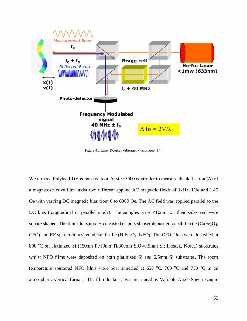
63
Figure 4.1 Laser Doppler Vibrometry technique [14].
We utilized Polytec LDV connected to a Polytec 5000 controller to measure the deflection (Δ) of
a magnetostrictive film under two different applied AC magnetic fields of 1kHz, 1Oe and 1.45
Oe with varying DC magnetic bias from 0 to 6000 Oe. The AC field was applied parallel to the
DC bias (longitudinal or parallel mode). The samples were <10mm on their sides and were
square shaped. The thin film samples consisted of pulsed laser deposited cobalt ferrite (CoFe2O4;
CFO) and RF sputter deposited nickel ferrite (NiFe2O4; NFO). The CFO films were deposited at
800 oC on platinized Si (150nm Pt/10nm Ti/300nm SiO2/0.5mm Si; Inostek, Korea) substrates
whilst NFO films were deposited on both platinized Si and 0.5mm Si substrates. The room
temperature sputtered NFO films were post annealed at 650 oC, 700
oC and 750
oC in an
atmospheric vertical furnace. The film thickness was measured by Variable Angle Spectroscopic
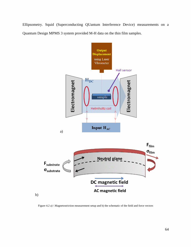
64
Ellipsometry. Squid (Superconducting QUantum Interference Device) measurements on a
Quantum Design MPMS 3 system provided M-H data on the thin film samples.
a)
b)
Figure 4.2 a) \ Magnetostriction measurement setup and b) the schematic of the field and force vectors
65
The samples were directly placed inside a Helmholtz coil of dimension 34mm width x 57mm
diameter with 28Ω coil resistance. The Helmholtz coil was placed between the poles of a GMW
Associates 3470 dipole electromagnet driven by a Kepco Model BOP 100-4M power supply.
Initially, a Polytec MSA 500 laser head was utilized but the displacement data with applied
magnetic field was noisy. The issue was found to be related to the effect of the magnetic fields
on the optomechanical mechanism inside the laser head. Polytec OFC 353 laser head which has a
depth of field of 450mm was next utilized but still presented challenges. It was found that a
minimum gap of 28” is required between the magnetic field systems (for a DC field of 6000 Oe
and 1.45Oe 1 kHz AC, the gap varies with strength of the fields) and the laser head of the
vibrometer. Despite this solution, it was noticed that nonmagnetic samples like Si substrate or a
platinized Si substrate showed finite displacement at 1kHz AC field. Further investigations led to
the finding that the laser vibrometer head, sample holder and magnetic Helmholtz coil plus
electromagnet system are coupled structurally and thus any mechanical displacement in one
system is propagated to the other influencing the magnetostriction measurement. Coils under an
AC current are known to vibrate commonly known as coil noise or coil hissing [15, 16]. Each of
the three components of the measurement setup, the coils, sample holder and the vibrometer had
to be mechanically isolated from each other in order to avoid the mechanical coupling. The
sample was loaded onto a 16” wooden spatula that was clamped to a shaker (with shorted coils)
capable of providing needed vibration isolation. The Helmholtz coil plus DC electromagnet
system was placed on an inflated inner tube and the laser was mounted on a tripod with rubber
feet.
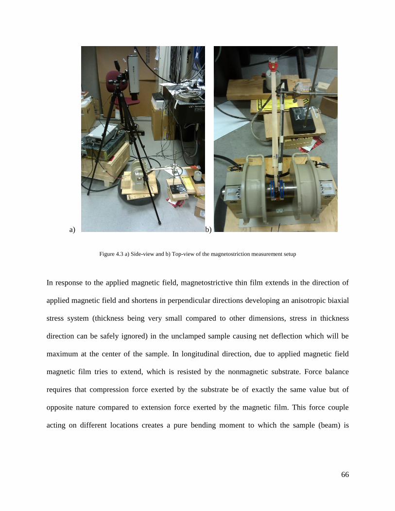
66
a) b)
Figure 4.3 a) Side-view and b) Top-view of the magnetostriction measurement setup
In response to the applied magnetic field, magnetostrictive thin film extends in the direction of
applied magnetic field and shortens in perpendicular directions developing an anisotropic biaxial
stress system (thickness being very small compared to other dimensions, stress in thickness
direction can be safely ignored) in the unclamped sample causing net deflection which will be
maximum at the center of the sample. In longitudinal direction, due to applied magnetic field
magnetic film tries to extend, which is resisted by the nonmagnetic substrate. Force balance
requires that compression force exerted by the substrate be of exactly the same value but of
opposite nature compared to extension force exerted by the magnetic film. This force couple
acting on different locations creates a pure bending moment to which the sample (beam) is

67
subjected. Pure bending moment acting on a beam of uniform cross-section area beam deforms it
in a circular arc. Radius of curvature of such an arc is given as:
2
2
2
2
ls
Rs
(1)
where ‘l’ is the chord length (sample length) and ‘s’ is the sagitta (the distance from the center of
the arc to the center of its base or chord) of the arc. The net vertical deflection Δ of the sample on
application of the AC varying magnetic field is assessed as the sagitta ‘s’. The deflection Δ of the
sample is calculated as the difference between the displacement ‘d’ measured by the LDV at 1Oe
and 1.45Oe AC magnetic field at each DC bias magnetic field condition per unit AC field. We
employed two AC field displacements for each DC magnetic bias so as to a) have a reference at
each DC bias level and b) reduce noise in the data.
2 1
1
2 1
2AC ACd d
s ACAC AC
(2)

68
Figure 4.4 Schematic of the induced curvature in sample due to applied magnetic force
Substituting Eqn. (2) in (1) provides the radius of curvature which is then used to calculate the
stress in the sample using force and bending moment balances [17]:
3 31
16 1
f f s s
sf f s f
Y t Y t
Rt t t
(3)
where Y is the Young’s modulus (1.5x10¹¹
N/m2 for CFO, 1.6x10
11 N/m
2 for NFO and
1.12x10¹¹
N/m2 for Si and platinized Si), ν is the Poisson’s ratio (0.2 for CFO, 0.3 for NFO and
0.28 for Si and 0.29 for platinized Si) and t is the thickness. From the above stress calculation,
we can then compute the magnetostriction in parallel or longitudinal mode (magnetic field and
strain in parallel) as:
21
f
ll
fY
(4)

69
For comparison, we use the magnetostriction relationship derived for substrate deflections
created by an anisotropic thin film stress generated in a magnetic field. This relationship was
derived for the specific case of magnetostriction of thin films[18]:
2
2
12
9 1
fs sll
f f s
Y t
Y t l
(5)
Results
The vertical displacements of the samples at 1 kHz AC magnetic fields of 1Oe and 1.45Oe are
shown in the table below:
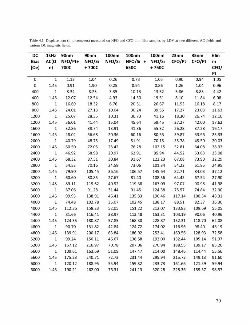
70
Table 4.1: Displacement (in picometers) measured on NFO and CFO thin film samples by LDV at two different AC fields and
various DC magnetic fields.
DC Bias (Oe)
1kHz AC(O
e)
90nm NFO/Pt+ 700C
90nm NFO/Si + 700C
100nm NFO/Si
100nm NFO/Si + 650C
100nm NFO/Si + 750C
23nm CFO/Pt
35nm CFO/Pt
66nm CFO/Pt
0 1 1.13 1.04 0.26 0.73 1.05 0.90 0.94 1.05
0 1.45 0.91 1.90 0.25 0.94 0.86 1.26 1.04 0.96
400 1 8.34 8.23 3.35 10.13 13.52 5.86 8.83 4.42
400 1.45 12.07 12.54 4.93 14.50 19.51 8.10 11.84 6.08
800 1 16.69 18.32 6.76 20.51 26.67 11.53 16.18 8.17
800 1.45 24.01 27.13 10.04 30.24 39.55 17.27 23.03 11.63
1200 1 25.07 28.35 10.31 30.73 41.16 18.30 26.74 12.10
1200 1.45 36.01 41.44 15.04 45.64 59.45 27.27 42.00 17.62
1600 1 32.86 38.74 13.91 41.36 55.32 26.28 37.28 16.17
1600 1.45 48.02 56.68 20.36 60.16 80.55 39.87 53.96 23.33
2000 1 40.79 48.75 17.49 51.91 70.15 35.78 45.50 20.03
2000 1.45 60.50 72.05 25.42 76.28 102.15 52.81 64.08 28.92
2400 1 46.92 58.98 20.97 62.91 85.94 44.52 53.63 23.08
2400 1.45 68.32 87.31 30.84 91.67 122.23 67.08 73.90 32.29
2800 1 54.53 70.16 24.59 73.06 101.34 54.22 61.85 24.95
2800 1.45 79.90 105.45 36.16 106.57 145.64 82.71 84.03 37.12
3200 1 60.60 80.85 27.67 81.40 108.56 64.45 67.54 27.90
3200 1.45 89.11 119.62 40.92 119.38 167.09 97.07 90.98 41.98
3600 1 67.06 91.28 31.44 91.45 124.38 75.57 74.84 32.30
3600 1.45 99.93 138.91 46.41 135.33 190.46 117.14 100.34 48.31
4000 1 74.48 102.78 35.07 102.45 138.17 88.51 82.37 36.30
4000 1.45 112.36 158.23 52.05 151.22 212.07 133.83 109.69 55.05
4400 1 81.66 116.41 38.97 113.48 153.31 103.19 90.06 40.96
4400 1.45 124.35 180.87 57.85 168.30 228.87 152.31 118.70 62.08
4800 1 90.70 131.82 42.84 124.72 174.02 116.96 98.40 46.19
4800 1.45 139.91 200.17 63.84 186.92 252.41 169.56 128.93 72.58
5200 1 99.24 150.11 46.67 136.58 192.00 132.44 105.14 51.37
5200 1.45 157.12 216.97 70.78 207.06 276.94 188.55 139.17 85.26
5600 1 109.61 163.69 51.09 147.47 214.00 148.46 114.44 55.56
5600 1.45 175.23 240.71 72.73 231.44 295.94 215.72 149.13 91.60
6000 1 120.12 188.95 55.94 159.32 233.73 161.66 121.59 59.94
6000 1.45 190.21 262.00 76.31 241.13 320.28 228.36 159.57 98.57
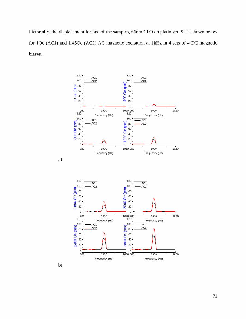
71
Pictorially, the displacement for one of the samples, 66nm CFO on platinized Si, is shown below
for 1Oe (AC1) and 1.45Oe (AC2) AC magnetic excitation at 1kHz in 4 sets of 4 DC magnetic
biases.
a)
980 1000 1020
0
20
40
60
80
100
120
980 1000 1020
0
20
40
60
80
100
120
980 1000 1020
0
20
40
60
80
100
120
980 1000 1020
0
20
40
60
80
100
120
0 O
e (
pm
)
Frequency (Hz)
AC1
AC2
400 O
e (
pm
)
Frequency (Hz)
AC1
AC2
800 O
e (
pm
)
Frequency (Hz)
AC1
AC21200 O
e (
pm
)
Frequency (Hz)
AC1
AC2
b)
980 1000 1020
0
20
40
60
80
100
120
980 1000 1020
0
20
40
60
80
100
120
980 1000 1020
0
20
40
60
80
100
120
980 1000 1020
0
20
40
60
80
100
120
1600 O
e (
pm
)
Frequency (Hz)
AC1
AC2
2000 O
e (
pm
)
Frequency (Hz)
AC1
AC2
2400 O
e (
pm
)
Frequency (Hz)
AC1
AC2
2800 O
e (
pm
)
Frequency (Hz)
AC1
AC2

72
c)
980 1000 1020
0
20
40
60
80
100
120
980 1000 1020
0
20
40
60
80
100
120
980 1000 1020
0
40
80
120
160
200
240
980 1000 1020
0
40
80
120
160
200
2403200 O
e (
pm
)Frequency (Hz)
AC1
AC2
3600 O
e (
pm
)
Frequency (Hz)
AC1
AC2
4000 O
e (
pm
)
Frequency (Hz)
AC1
AC2
4400 O
e (
pm
)
Frequency (Hz)
AC1
AC2
d)
980 1000 1020
0
40
80
120
160
200
240
980 1000 1020
0
40
80
120
160
200
240
980 1000 1020
0
40
80
120
160
200
240
980 1000 1020
0
40
80
120
160
200
240
4800 O
e (
pm
)
Frequency (Hz)
AC1
AC2
5200 O
e (
pm
)
Frequency (Hz)
AC1
AC2
5600 O
e (
pm
)
Frequency (Hz)
AC1
AC2
6000 O
e (
pm
)
Frequency (Hz)
AC1
AC2
Figure 4.5 Displacement vs. frequency for 1Oe (AC1) and 1.45Oe (AC2) for the 66nm CFO thin film on platinized Si at DC bias
of a) 0-1200 Oe b) 1600-2800 Oe c) 3200-4400 Oe and d) 4800-6000 Oe.
The data in Table 4.1 was processed by using Eqns. (1)-(5) to generate the magnetostriction
results shown below:
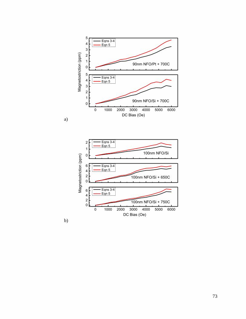
73
a)
0
1
2
3
4
5
0 1000 2000 3000 4000 5000 6000
0
1
2
3
4
5
Magneto
str
iction (
ppm
)
90nm NFO/Pt + 700C
Eqns 3-4
Eqn 5
90nm NFO/Si + 700C
DC Bias (Oe)
Eqns 3-4
Eqn 5
b)
0
1
2
0
2
4
6
0 1000 2000 3000 4000 5000 6000
0
2
4
6
100nm NFO/Si
Eqns 3-4
Eqn 5
100nm NFO/Si + 650C
Eqns 3-4
Eqn 5
Magneto
str
iction (
ppm
)
100nm NFO/Si + 750C
DC Bias (Oe)
Eqns 3-4
Eqn 5

74
c)
0
2
4
6
8
0
2
4
6
8
0 1000 2000 3000 4000 5000 6000
0
2
4
6
Magneto
str
iction (
ppm
) 23nm CFO/Pt
Eqns 3-4
Eqn 5
35nm CFO/Pt
Eqns 3-4
Eqn 5
66nm CFO/Pt
DC Bias (Oe)
Eqns 3-4
Eqn 5
Figure 4.6 Magnetostriction (λ) calculated using equations 3-4 and 5 for a) NFO on Si vs.Platinized Si b) NFO on Si as-
deposited, after 650C and 750C anneal and c) CFO on Platinized Si
Discussion
The Magnetostriction data calculated using equations 3-4 and 5 are almost similar with
that from the latter predicting slightly higher values. Magnetization (M) – Magnetic Field(H)
hysteresis loops were measured in the longitudinal direction using VSM (Table 4.3) to determine
the remnant magnetization (Mr), coercive magnetic field (Hc), saturation magnetic field (Hsat)
and saturation magnetization (Msat). The applied DC bias, HDC, of 0-6000 Oe during λ
measurement, did not cause the thin films to reach saturation magnetization. Single crystal Si is
considered diamagnetic whilst Pt thin film is paramagnetic. For the soft magnetic NFO films
deposited on Si and platinized Si respectively, the Mr and Hc is higher on Si whilst Hsat and Msat
is lower. The magnitude of parameters Mr , Hsat and Msat increases slightly with annealing
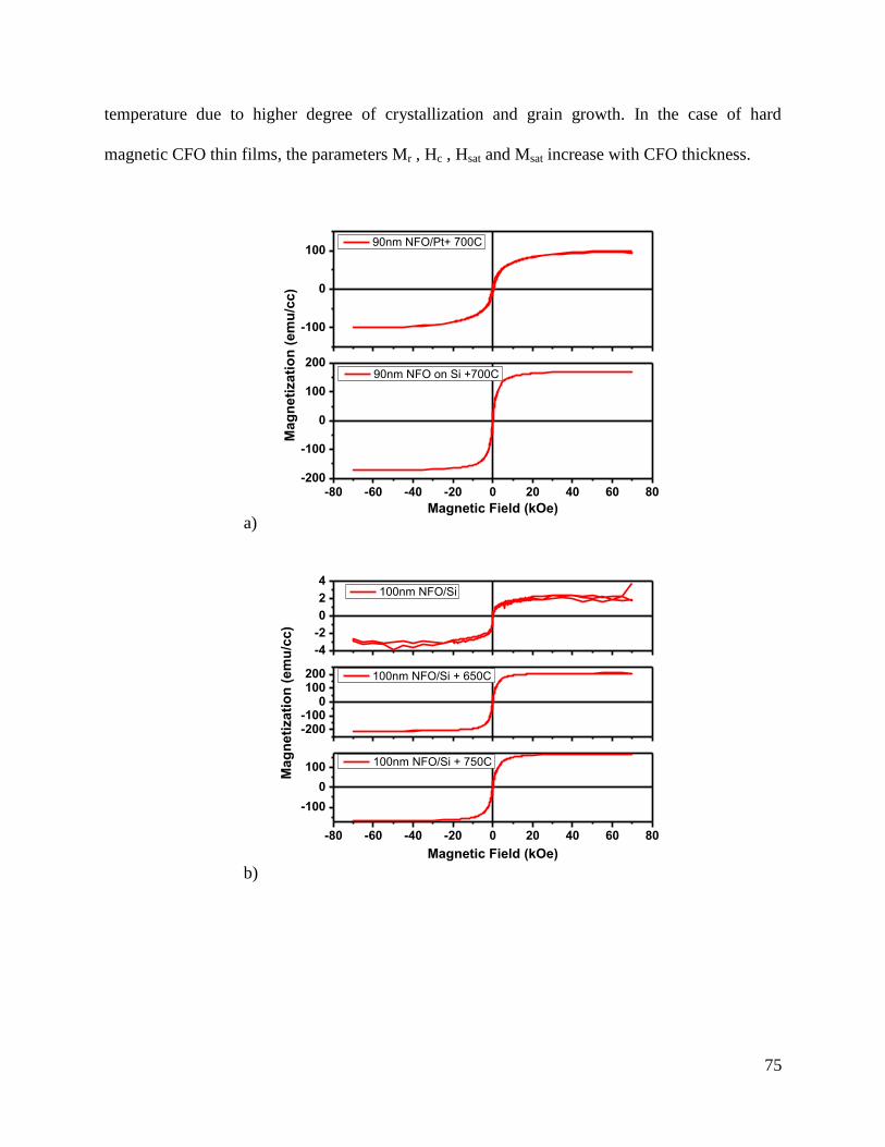
75
temperature due to higher degree of crystallization and grain growth. In the case of hard
magnetic CFO thin films, the parameters Mr , Hc , Hsat and Msat increase with CFO thickness.
a)
-100
0
100
-80 -60 -40 -20 0 20 40 60 80-200
-100
0
100
200
Mag
neti
zati
on
(em
u/c
c)
90nm NFO/Pt+ 700C
Magnetic Field (kOe)
90nm NFO on Si +700C
b)
-4
-2
0
2
4
-200-100
0100200
-80 -60 -40 -20 0 20 40 60 80
-100
0
100
100nm NFO/Si
Mag
neti
zati
on
(em
u/c
c)
100nm NFO/Si + 650C
Magnetic Field (kOe)
100nm NFO/Si + 750C

76
c)
-100
0
100
-200
-100
0
100
200
-80 -60 -40 -20 0 20 40 60 80
-200-100
0100200
23nm CFO/Pt
Mag
neti
zati
on
(em
u/c
c)
35nm CFO/Pt
Magnetic Field (kOe)
66nm CFO/Pt
Figure 4.7 M-H hysteresis loops for a) NFO on Si vs.Platinized Si b) NFO on Si as-deposited, after 650C and 750C anneal and c)
CFO on Platinized Si
Table 4.2 Hysteresis loop data obtained from VSM measurement for NFO and CFO thin film samples.
Mr (emu/cc) Hc(Oe) Hsat(kOe) Msat (emu/cc)
90nm NFO/Pt + 700C 10.54 463.00 55.32 96.19
90nm NFO/Si + 700C 19.70 165.50 39.74 33.95
100nm NFO/Si - - 38.74 4.952
100nm NFO/Si + 650C 18.79 189.50 42.13 33.728
100nm NFO/Si + 750C 28.55 187.50 49.76 41.694
23nm CFO/Pt 49.47 1453.00 44.40 134.14
35nm CFO/Pt 57.05 1911.00 54.67 185.75
66nm CFO/Pt 70.24 1944.50 69.50 195.70
NFO magnetostriction data mostly match the trends observed in its M-H data. NFO films on
Platinized Si have higher λ (and high Msat) whilst for films on Si, the annealing temperature in
the range of 650-750 °C causes a small proportional increase in magnetostriction and
magnetization properties. Magnetostriction λ of CFO decreases with thickness but M-H
properties as measured by VSM increase (as shown in table above). CFO has been known to

77
possess both large magnetic anisotropy and large anisotropic magnetostriction [19]. Saturation
magnetization should be a constant because it is the property of a material. If it is changing for
different thickness it might be that the saturation fields are different. This may occur due to film
defects and substrate clamping of domains. However remnant magnetization can change with
total magnetic anisotropy. From X-ray diffraction studies (shown below), it was found that the
NFO films are slightly textured on Si and platinized Si but NFO texturing improves by 50% with
annealing temperature. For CFO, the texturing improves with thickness, where films with >35nm
were found to reach same degree of 20% texturing with annealing. So the λ values in the films
studied here are expected to be lower than that for fully textured or epitaxial films. Prior results
on CFO have shown a λsat of 110ppm [20] whilst that for NFO the magnitude reaches up to
26ppm [21].
a)
15 20 25 30 35 40 45 50 55 60 65
0
160
320
480
0
190
380
570
0
120
240
360
2theta (degree)
100nm NFO/Si
Si
Inte
nsity (
arb
.units) 100nm NFO/Si + 650C
(40
0)
(51
1)
100nm NFO/Si + 750C
(31
1)
(22
0)

78
b)
15 20 25 30 35 40 45 50 55 60 6510
0
101
102
103
104
105
106
0
170
340
510
(31
1)
(31
1)
Si TiO
Pt
Si
(51
1)
(51
1)
2degree)
90nm NFO/Pt
Inte
nsity (
arb
.un
its)
90nm NFO/Si + 700C
c)
15 20 25 30 35 40 45 50 55 60 6510
0
101
102
103
104
105
106
107
100
101
102
103
104
105
106
107
100
101
102
103
104
105
106
107
2degree)
23nm CFO/Pt
Pt
Si TiO
Inte
nsity (
arb
.un
its) 35nm CFO/Pt
66nm CFO/Pt
(31
1)
(51
1)
Figure 4.8 XRD plots for a) NFO on Si vs. annealing temperature b) NFO on Si vs. Platinized Si c) CFO on Platinized Si vs.
Thickness

79
The magnetostriction measurement technique presented here is highly dependent on the
mechanical constants for the film and substrate utilized in equations (3-4). The Young’s modulus
of silicon can vary in the range of 1.25-2.02 x10¹¹
N/m2 based on the crystalline orientation of
wafer and doping [22]. In the calculations reported here, the modulus value of 1.69x10¹¹
N/m2
for a silicon (100) wafer was used with the axis of bending along [110] direction [23]. The
magnetization of a magnetostrictive thin film can be derived from the radius of curvature
induced by the magnetic moment (magnetization x volume) applied by a magnetic field [5, 7] as:
3
12
s sY t bm
RB (6)
Substituting the radius of curvature calculated using Eqn. (1) in the above equation and
comparing the resultant magnetic moment values to the M-H VSM data a baseline can be
established However, the above equation was derived for the torque created due to an AC field
perpendicular to a DC magnetic field (perpendicular mode). For the parallel mode configuration,
as both the ac and dc fields are applied parallel to the length of the sample, there will be equal
and opposite torques at the ends of the sample in a direction perpendicular to the sample and
along its width.

80
a)
0 1000 2000 3000 4000 5000 60000
5
10
15
0 1000 2000 3000 4000 5000 60000
102030405060
0 1000 2000 3000 4000 5000 60000
102030405060
100nm
NF
O/S
i (e
mu/c
c)
DC Bias (Oe)
MS
VSM
100nm
NF
O 7
50C
/Si (e
mu/c
c)
DC Bias (Oe)
MS
VSM
100nm
NF
O 6
50C
/Si (e
mu/c
c)
DC Bias (Oe)
MS
VSM
b)
0 1000 2000 3000 4000 5000 60000
10
20
30
40
50
60
0 1000 2000 3000 4000 5000 60000
10
20
30
40
90
nm
NF
O/P
t (e
mu
/cc)
DC Bias (Oe)
MS
VSM
90
nm
NF
O/S
i (e
mu
/cc)
DC Bias (Oe)
MS
VSM
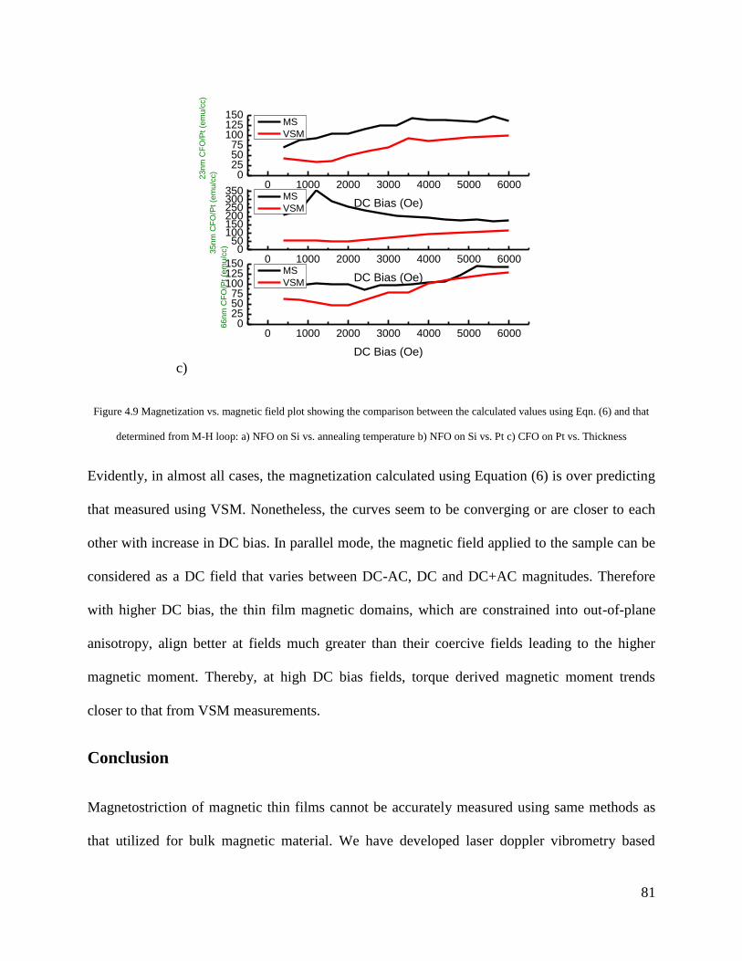
81
c)
0 1000 2000 3000 4000 5000 60000
255075
100125150
0 1000 2000 3000 4000 5000 60000
50100150200250300350
0 1000 2000 3000 4000 5000 60000
255075
100125150
23nm
CF
O/P
t (e
mu/c
c)
DC Bias (Oe)
MS
VSM
35nm
CF
O/P
t (e
mu/c
c)
DC Bias (Oe)
MS
VSM
66nm
CF
O/P
t (e
mu/c
c)
DC Bias (Oe)
MS
VSM
Figure 4.9 Magnetization vs. magnetic field plot showing the comparison between the calculated values using Eqn. (6) and that
determined from M-H loop: a) NFO on Si vs. annealing temperature b) NFO on Si vs. Pt c) CFO on Pt vs. Thickness
Evidently, in almost all cases, the magnetization calculated using Equation (6) is over predicting
that measured using VSM. Nonetheless, the curves seem to be converging or are closer to each
other with increase in DC bias. In parallel mode, the magnetic field applied to the sample can be
considered as a DC field that varies between DC-AC, DC and DC+AC magnitudes. Therefore
with higher DC bias, the thin film magnetic domains, which are constrained into out-of-plane
anisotropy, align better at fields much greater than their coercive fields leading to the higher
magnetic moment. Thereby, at high DC bias fields, torque derived magnetic moment trends
closer to that from VSM measurements.
Conclusion
Magnetostriction of magnetic thin films cannot be accurately measured using same methods as
that utilized for bulk magnetic material. We have developed laser doppler vibrometry based

82
technique to measure the picometer level deflections occurring in square-shaped
magnetostrictive thin films deposited on Si and platinized Si substrates. We disclose the
precautions necessary to make such delicate measurements especially the isolation required
between the 3 components of the measurements setup, namely, sample, laser and magnetic coils.
We corroborate our approach by comparing the magnetization calculated from the radius of
curvature induced by the magnetically induced torque on the sample vs. that measured by a VSM
system. This non-contact technique can provide advantages in routine optimization of the
magnetostrictive composition.
Acknowledgements: The authors gratefully acknowledge the financial support from Air Force
Office of Scientific Research (AFOSR) through Young Investigator Program. We would
like to thank Greg Pribil of J. A. Woollam Inc. for help with modeling of the thin film VASE
data. We are also greatly indebted to CEHMS colleagues Justin Farmer and SuChul Yang for
assistance with the experimental setup.
References
[1] Ekreem NB, Olabi AG, Prescott T, Rafferty A, Hashmi MSJ. An overview of
magnetostriction, its use and methods to measure these properties. Journal of Materials
Processing Technology 2007;191:96.
[2] Grössinger R, Sassik H, Holzer D, Pillmayr N. Accurate measurement of the
magnetostriction of soft magnetic material. Proc. 1&2—Dimensional Magnetic Measurement
and Testing 2000:35.
[3] Raghunathan A, Snyder JE, Jiles DC. Comparison of Alternative Techniques for
Characterizing Magnetostriction and Inverse Magnetostriction in Magnetic Thin Films.
Magnetics, IEEE Transactions on 2009;45:3269.
[4] Marcus PM. Magnetostrictive bending of a cantilevered film-substrate system. Journal of
Magnetism and Magnetic Materials 1997;168:18.
[5] Sander D, Enders A, Kirschner J. Magnetization, magnetostriction and film stress of Fe
monolayers on W(100). Magnetics, IEEE Transactions on 1998;34:2015.
83
[6] du Trémolet de Lacheisserie E, Peuzin JC. Magnetostriction and internal stresses in thin
films: the cantilever method revisited. Journal of Magnetism and Magnetic Materials
1994;136:189.
[7] Weber M, Koch R, Rieder KH. UHV Cantilever Beam Technique for Quantitative
Measurements of Magnetization, Magnetostriction, and Intrinsic Stress of Ultrathin Magnetic
Films. Physical Review Letters 1994;73:1166.
[8] Bellesis GH, Harlee PS, III, Renema A, II, Lambeth DN. Magnetostriction measurement
by interferometry. Magnetics, IEEE Transactions on 1993;29:2989.
[9] Tam AC, Schroeder H. A new high-precision optical technique to measure
magnetostriction of a thin magnetic film deposited on a substrate. Magnetics, IEEE Transactions
on 1989;25:2629.
[10] Adhikari R, Kaundal R, Sarkar A, Rana P, K. Das A. The cantilever beam magnetometer:
A simple teaching tool for magnetic characterization. American Journal of Physics 2012;80:225.
[11] Adhikari R, Sarkar A, Das AK. A versatile cantilever beam magnetometer for ex situ
characterization of magnetic materials. Review of Scientific Instruments 2012;83:013903.
[12] Castellini P, Martarelli M, Tomasini EP. Laser Doppler Vibrometry: Development of
advanced solutions answering to technology's needs. Mechanical Systems and Signal Processing
2006;20:1265.
[13] Nakata T, Takahashi N, Nakano M, Muramatsu K, Miyake P. Magnetostriction
measurements with a laser Doppler velocimeter. Magnetics, IEEE Transactions on
1994;30:4563.
[14] www.polytec.com.
[15] Roozen NB, Koevoets AH, den Hamer AJ. Active Vibration Control of Gradient Coils to
Reduce Acoustic Noise of MRI Systems. Mechatronics, IEEE/ASME Transactions on
2008;13:325.
[16] http://en.wikipedia.org/wiki/Coil_noise.
[17] Ohring M. Materials science of thin films : deposition and structure. San Diego, CA:
Academic Press, 2002.
[18] van de Riet E. Deflection of a substrate induced by an anisotropic thin-film stress. Journal
of Applied Physics 1994;76:584.
[19] Hu G. Structural tuning of the magnetic behavior in spinel-structure ferrite thin films.
Physical review. B, Condensed matter 2000;62:R779.
[20] O'Handley RC. Magnetostrictive Materials and Magnetic Shape Memory Materials.
Handbook of Magnetism and Advanced Magnetic Materials. John Wiley & Sons, Ltd, 2007.
[21] Cullity BD, Graham CD. Soft Magnetic Materials. Introduction to Magnetic Materials.
John Wiley & Sons, Inc., 2008. p.439.
[22] p.http://www.memsnet.org/material/siliconsibulk/.
[23] Fang H-B, Liu J-Q, Xu Z-Y, Dong L, Wang L, Chen D, Cai B-C, Liu Y. Fabrication and
performance of MEMS-based piezoelectric power generator for vibration energy harvesting.
Microelectronics Journal 2006;37:1280.
84
Chapter 5
Thermal Transport in Textured Lead Zirconate Titanate
Thin Films
Ronnie Varghesea, Hari Harikrishna
b, Scott T. Huxtable
c, W. T. Reynolds Jr.
a and Shashank Priya
d
a Department of Materials Science, Virginia Tech, Blacksburg, Virginia, 24061, USA
b Department of Engineering Science and Mechanics, Virginia Tech, Blacksburg, Virginia, 24061, USA
c Department of Mechanical Engineering, Virginia Tech, Blacksburg, Virginia, 24061, USA
d Center for Energy Harvesting Materials and Systems (CEHMS), Bio-inspired Materials and Devices Laboratory (BMDL), Virginia Tech,
Blacksburg, Virginia, 24061, USA
Abstract
We use Time Domain Thermoreflectance (TDTR) to characterize a series of textured
Pb(Zr,Ti)O3 (PZT) thin films grown by a sol gel process on platinized silicon substrates. These
PZT films have preferred crystallographic orientations of (100), (110), and (111) which we
control by manipulating the heterogeneous nucleation and growth characteristics at the interface
between the film and the underlying Pt layer on the substrate. TDTR was used to measure both
the PZT film thermal conductivity and the interface thermal conductance between the PZT and
Pt as well as that between the PZT and an Al thermoreflectance layer evaporated on the PZT
surface. We find that thermal conductivity and interface thermal conductance have a slight
dependence on crystal orientation. Thus with our nanoscale thermal measurements we can
discriminate between PZT samples of different crystallographic orientations.. The thermal
conductivities of the PZT films with different crystal orientations are in the range of 1.45 - 1.70

85
W m-1
K-1
. The interface thermal conductance between the PZT and Pt layer ranges from 40 - 65
MW m-2
K-1
, while the conductance between the Al thermoreflectance layer and PZT is ~100
MW m-2
K-1
.
Keywords: Thin films; thermal conductivity; thermal conductance; Interface properties; texturing
Introduction
Crystallographic texturing of Pb(Zr,Ti)O3 (PZT) thin films on platinized Si substrates
(Pt/Ti/SiO2/Si) has been studied extensively and various mechanisms related to the origin of the
preferred orientation have been proposed in the literature [1-9]. The single most important factor
for the nucleation and growth of a preferentially oriented PZT film is the interaction of the PZT
precursors with the top layer of the substrate, namely Pt in case of a platinized silicon substrate.
The boundary conditions at the PZT-Pt interface determine the overall degree of texturing that
can be achieved in the PZT films. Prior research has investigated the role of interfacial transient
phases of an intermetallic Pt-Pb [1, 3, 5], pyrochlore Pb2(Zr,Ti)2O6 [5-7], permanent buffer or
seed layers of PbTiO3 [2, 4, 8], TiO2 [9], ZrO2 [9], and PbO [1] concentration gradients on the
evolution of texture. However, the deterministic criterion controlling the magnitude of texture
degree remains a debatable subject.
In a prior study, we characterized the phase and orientation of sol-gel derived
Pb(Zr0.6Ti0.4)O3 thin films and developed the Temperature-Time-Transformation (TTT) diagrams
illustrating the correlation between the synthesis parameters and Lotgering factor. Analytical
models were developed to utilize the TTT diagrams effectively [10]. However, the earlier study’s
focus was not the investigation of the interfacial heterogeneity in the PZT films that could shed

86
light on the mechanism responsible for development of texture. Various characterization
techniques with increasing sensitivity including optical (Ellipsometry and Raman)
characterization, high resolution binding energy X-ray photoelectron spectroscopy depth profile
scans, and High Resolution Transmission Electron Microscopy (HR-TEM) were utilized to study
the interface between PZT and Pt, but nothing significant was found. Building upon the prior
work, here we use an optical technique called Time Domain Thermoreflectance (TDTR) to
measure the interface thermal conductance, G, between the textured PZT films and the
underlying Pt layer, along with the interface thermal conductance between the PZT and an Al
layer that is evaporated on the PZT films. We also use TDTR to simultaneously extract the
thermal conductivity, k, of the textured PZT films. The variation in the magnitude of thermal
conductance could be utilized for inferring the structural changes occurring at the interface.
Hopkins et al. [11] used TDTR to examine the thermal conductance at Al/Si and
Al/sapphire interfaces with different Si and sapphire substrate orientations. They found that the
interface thermal conductance for the sapphire samples (trigonal unit cell) showed a strong
dependence on the crystal orientation while that was not the case with silicon samples (diamond
cubic unit cell). The interface thermal conductance dependence on the crystal orientation in the
Al/sapphire samples was attributed to the anisotropy in the Brillouin zone and subsequent
changes in the phonon velocities with crystallographic direction in the sapphire. Costescu et al.
[12] also used TDTR to measure the interface thermal conductance of TiN:MgO (001) and
TiN:MgO (111), and they found no dependence on crystallographic orientation. More recently,
Duda et al. [13] used classical molecular dynamics simulations to study the influence of
crystallographic orientation on interface thermal conductance. They found that the thermal
conductance at interfaces between two cubic materials was independent of crystallographic
87
orientation, while the conductance between a face centered cubic material and a tetragonal
material had a dependence on orientation.
With TDTR we find a slight dependence on the thermal conductivity with the
crystallographic orientation of the PZT films and observe differences in the interface thermal
conductance between the PZT and Pt for varying degree of preferred orientations (100), (110),
and (111). However, we do not observe a strong correlation between the interface thermal
conductance and the preferred orientation.
Sample Preparation and Characterization
The PZT thin film (Zr/Ti = 60/40) samples were synthesized by sol-gel processing as
described in detail elsewhere [10]. With this technique, a series of films were synthesized and
crystallized to achieve varying percentages of crystallographic orientations (111), (110), and
(100). The crystallographic orientation and thickness of the samples was determined by X-ray
diffraction (Phillips Xpert Pro) and Variable Angle Spectroscopic Ellipsometry (J.A. Woollam),
respectively. All of the samples had a rhombohedral crystal structure at room temperature.
Transmission electron microscopy (TEM) was performed with an FEI Titan 300. Samples for
TEM were prepared using a focused ion beam from an FEI Helios 600 NanoLab. Raman spectra
was collected using a Jobin-Yvon T6400 Triplemate with 514.5 nm radiation. GI-XRD data was
collected on a Bruker D8 Advance system with an incident Goebel mirror having a 4 degree
Soller slit and 0.6mm exit slit. The diffracted beam side of the diffractometer was equipped with
an equatorial Soller slit (0.2 degree divergence) and LynxEye detector in 0d mode. Data was
collected using 2 theta scans with fixed grazing incidence (either 4 or 6 degree incident angle).
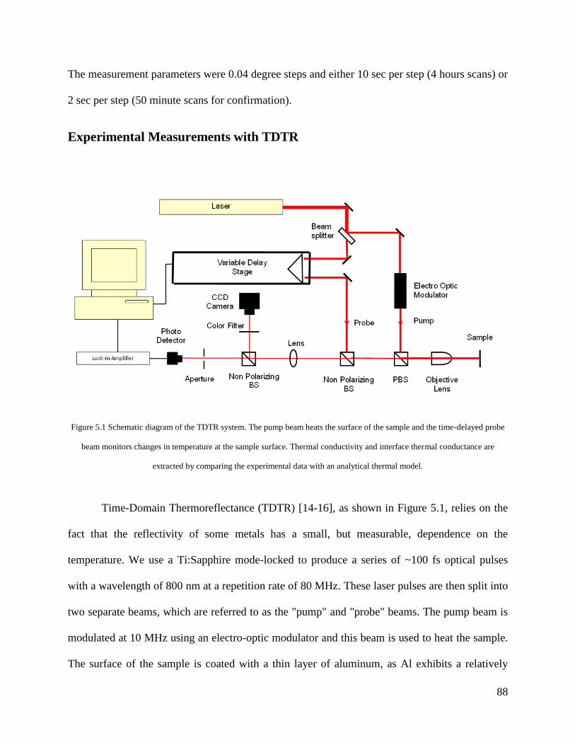
88
The measurement parameters were 0.04 degree steps and either 10 sec per step (4 hours scans) or
2 sec per step (50 minute scans for confirmation).
Experimental Measurements with TDTR
Figure 5.1 Schematic diagram of the TDTR system. The pump beam heats the surface of the sample and the time-delayed probe
beam monitors changes in temperature at the sample surface. Thermal conductivity and interface thermal conductance are
extracted by comparing the experimental data with an analytical thermal model.
Time-Domain Thermoreflectance (TDTR) [14-16], as shown in Figure 5.1, relies on the
fact that the reflectivity of some metals has a small, but measurable, dependence on the
temperature. We use a Ti:Sapphire mode-locked to produce a series of ~100 fs optical pulses
with a wavelength of 800 nm at a repetition rate of 80 MHz. These laser pulses are then split into
two separate beams, which are referred to as the "pump" and "probe" beams. The pump beam is
modulated at 10 MHz using an electro-optic modulator and this beam is used to heat the sample.
The surface of the sample is coated with a thin layer of aluminum, as Al exhibits a relatively
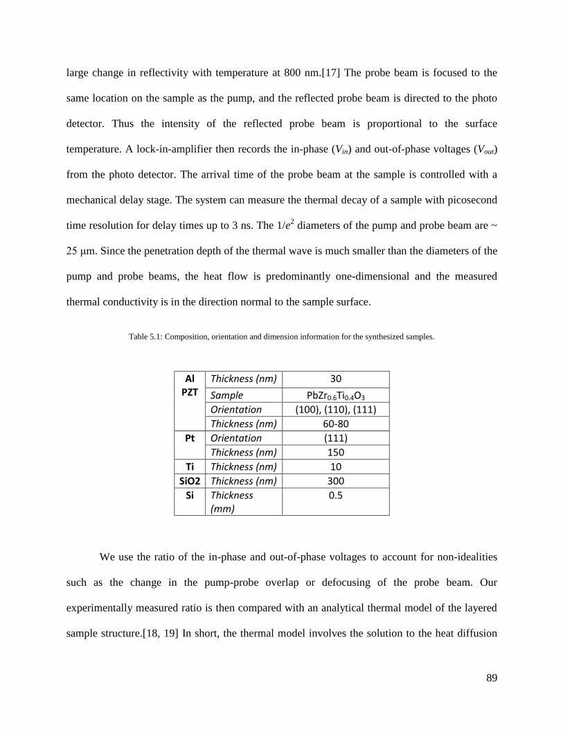
89
large change in reflectivity with temperature at 800 nm.[17] The probe beam is focused to the
same location on the sample as the pump, and the reflected probe beam is directed to the photo
detector. Thus the intensity of the reflected probe beam is proportional to the surface
temperature. A lock-in-amplifier then records the in-phase (Vin) and out-of-phase voltages (Vout)
from the photo detector. The arrival time of the probe beam at the sample is controlled with a
mechanical delay stage. The system can measure the thermal decay of a sample with picosecond
time resolution for delay times up to 3 ns. The 1/e2 diameters of the pump and probe beam are ~
25 μm. Since the penetration depth of the thermal wave is much smaller than the diameters of the
pump and probe beams, the heat flow is predominantly one-dimensional and the measured
thermal conductivity is in the direction normal to the sample surface.
Table 5.1: Composition, orientation and dimension information for the synthesized samples.
Al PZT
Thickness (nm) 30
Sample PbZr0.6Ti0.4O3
Orientation (100), (110), (111)
Thickness (nm) 60-80
Pt Orientation (111)
Thickness (nm) 150
Ti Thickness (nm) 10
SiO2 Thickness (nm) 300
Si Thickness (mm)
0.5
We use the ratio of the in-phase and out-of-phase voltages to account for non-idealities
such as the change in the pump-probe overlap or defocusing of the probe beam. Our
experimentally measured ratio is then compared with an analytical thermal model of the layered
sample structure.[18, 19] In short, the thermal model involves the solution to the heat diffusion

90
equation for the surface temperature of the sample under periodic heating. The unknown
parameters (k and/or G) are adjusted until satisfactory matching is found between the model and
the thermoreflectance measurements. The model requires the thickness, heat capacity, and
thermal conductivity of each layer of the sample, and the details of the sample structure as given
in Table 5.1. The thermal conductivities of the aluminum and platinum films were measured
using the Wiedemann-Franz law and were found to be 180 W m-1
K-1
and 70 W m-1
K-1
,
respectively. These values are reduced slightly from their bulk values, since the films are thin.
The thermal conductivities of the titanium and oxide layers, and the heat capacities of all layers
except PZT were taken to be the same as bulk values. The heat capacity of the PZT layer is
assumed to be 2.4 MJ/(m3-K) from our measurements of density and using specific heat
measurements on similar PZT materials by Lang et al. [20]
With this sample configuration, we are initially left with five unknowns in the thermal
model: the interface thermal conductance between aluminum and PZT, G1, the thermal
conductivity of the PZT layer, kPZT, the interface thermal conductance between PZT and
platinum, G2, the interface thermal conductance between platinum and titanium, G3, and the
interface thermal conductance between Ti and the oxide layer, G4. The interface thermal
conductance at metal-metal interfaces is on the order of several hundred MW m-2
K-1
, beyond the
range of the sensitivity of our measurements, thus we can ignore G3 in our analysis.[21] To
further reduce the number of unknowns, we examined a reference sample without the PZT layer
and found the interface thermal conductance between titanium and the oxide layer, G4, to be
~110 MW m-2
K-1
. The remaining three remaining unknowns, G1, kPZT, and G2, each affect the
data in a unique manner. In the model, G1 changes the radius of curvature below delay times of
~0.5 ns, while G2 offsets the amplitude of the signal by an approximately constant value, and
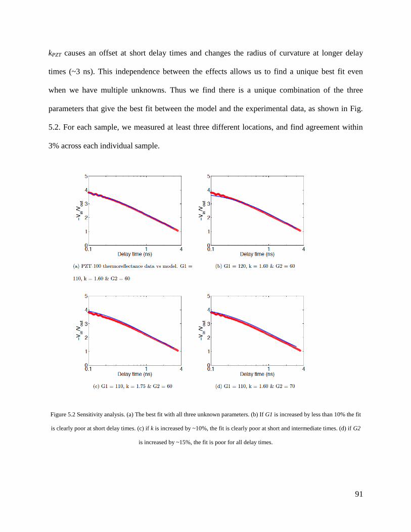
91
kPZT causes an offset at short delay times and changes the radius of curvature at longer delay
times (~3 ns). This independence between the effects allows us to find a unique best fit even
when we have multiple unknowns. Thus we find there is a unique combination of the three
parameters that give the best fit between the model and the experimental data, as shown in Fig.
5.2. For each sample, we measured at least three different locations, and find agreement within
3% across each individual sample.
Figure 5.2 Sensitivity analysis. (a) The best fit with all three unknown parameters. (b) If G1 is increased by less than 10% the fit
is clearly poor at short delay times. (c) if k is increased by ~10%, the fit is clearly poor at short and intermediate times. (d) if G2
is increased by ~15%, the fit is poor for all delay times.

92
Experimental Results
The pyrolysis and annealing temperatures and times along with the resulting texturing,
i.e. the relative crystallographic orientations, of the sol-gel PZT thin films are summarized in
Table 5.2.
Table 5.2 X-ray diffraction analysis results for the PZT samples
Orientation Sample No.
Pyrolysis Temperature
(°C)
Pyrolysis Time (min)
Annealing Temperature
(°C)
Annealing Time (min)
(100) (110) (111)
4D 250 1.5 625 60 72% 28% 0% 64 300 3 675 45 77% 23% 0% 67 300 3 725 30 97% 3% 0% 6A 300 3 775 15 93% 7% 0% 62 250 1.5 675 15 0% 9% 91% 72 250 1.5 800 60 0% 3 % 97% 76 250 1.5 750 60 0% 4% 96 %
4F 0 0 675 20 8% 92% 0% 7B 0 0 650 45 6% 94% 0% 81 0 0 800 45 0% 100% 0% 68 300 3 775 45 39% 20% 41% 7D 0 0 700 45 49% 1% 50%
An XPS depth profile showed decreasing amounts of Pb, Zr, Ti and O with depth whilst
Pt increases with depth. Interestingly, because of surface roughness of the sputter crater created
by the Argon sputter gas’s unequal sputtering rate of elements in PZT, the Pt is detected at the
surface and masks the Ti detection. Therefore the detection of an interfacial seeding layer was
ruled out by this technique.
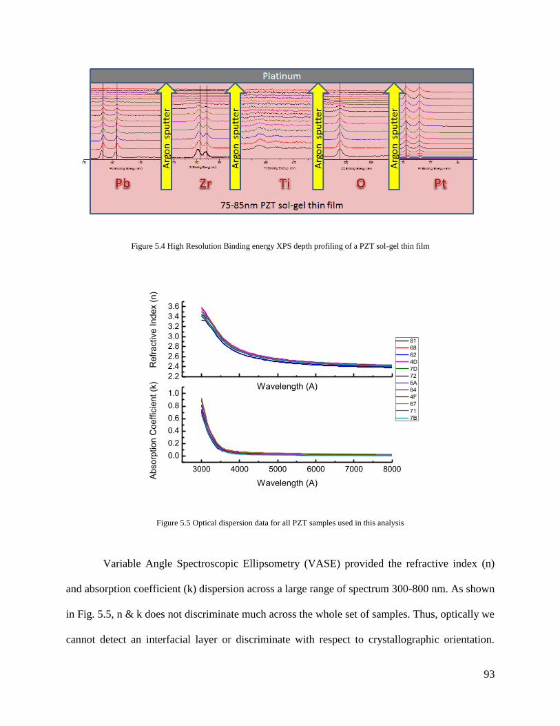
93
Figure 5.4 High Resolution Binding energy XPS depth profiling of a PZT sol-gel thin film
2.2
2.4
2.6
2.8
3.0
3.2
3.4
3.6
3000 4000 5000 6000 7000 8000
0.0
0.2
0.4
0.6
0.8
1.0
81
68
62
4D
7D
72
6A
64
4F
67
71
7B
Re
fra
ctive
In
de
x (
n)
Wavelength (A)
Ab
so
rptio
n C
oe
ffic
ien
t (k
)
Wavelength (A)
Figure 5.5 Optical dispersion data for all PZT samples used in this analysis
Variable Angle Spectroscopic Ellipsometry (VASE) provided the refractive index (n)
and absorption coefficient (k) dispersion across a large range of spectrum 300-800 nm. As shown
in Fig. 5.5, n & k does not discriminate much across the whole set of samples. Thus, optically we
cannot detect an interfacial layer or discriminate with respect to crystallographic orientation.
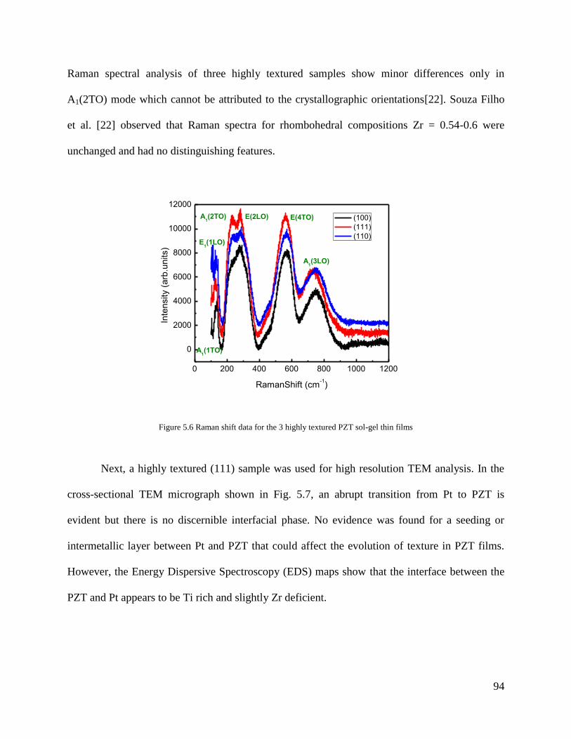
94
Raman spectral analysis of three highly textured samples show minor differences only in
A1(2TO) mode which cannot be attributed to the crystallographic orientations[22]. Souza Filho
et al. [22] observed that Raman spectra for rhombohedral compositions Zr = 0.54-0.6 were
unchanged and had no distinguishing features.
0 200 400 600 800 1000 1200
0
2000
4000
6000
8000
10000
12000
Inte
nsity (
arb
.units)
RamanShift (cm-1)
(100)
(111)
(110)
A1(2TO) E(2LO)
A1(1TO)
E1(1LO)
E(4TO)
A1(3LO)
Figure 5.6 Raman shift data for the 3 highly textured PZT sol-gel thin films
Next, a highly textured (111) sample was used for high resolution TEM analysis. In the
cross-sectional TEM micrograph shown in Fig. 5.7, an abrupt transition from Pt to PZT is
evident but there is no discernible interfacial phase. No evidence was found for a seeding or
intermetallic layer between Pt and PZT that could affect the evolution of texture in PZT films.
However, the Energy Dispersive Spectroscopy (EDS) maps show that the interface between the
PZT and Pt appears to be Ti rich and slightly Zr deficient.
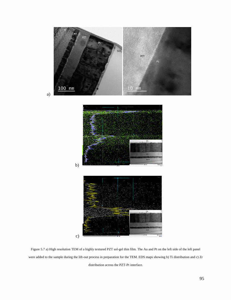
95
a)
b)
c)
Figure 5.7 a) High resolution TEM of a highly textured PZT sol-gel thin film. The Au and Pt on the left side of the left panel
were added to the sample during the lift-out process in preparation for the TEM. EDS maps showing b) Ti distribution and c) Zr
distribution across the PZT-Pt interface.

96
TDTR measurements from the textured PZT samples listed in Table 5.2 were modeled as
mentioned in last section to provide the results in Table 5.3.
Table 5.3 TDTR results from the PZT samples
Sample No.
(100)
Orientation (110)
(111)
GAl-PZT (MW/m2-K)
kPZT (W/m-K)
GPZT-Pt (MW/m2-K)
G1/k G2/k
4D 72% 28% 0% 110 1.60 50 68.75 31.25 64 77% 23% 0% 110 1.60 60 68.75 37.50
67 97% 3% 0% 110 1.65 60 66.67 36.36 6A 93% 7% 0% 110 1.65 60 66.67 36.36 62 0% 9% 91% 100 1.70 60 58.82 35.29 72 0% 3 % 97% 100 1.70 50 58.82 29.41 76 0% 4% 96 % 100 1.70 50 58.82 29.41 4F 8% 92% 0% 90 1.50 40 60.00 26.67 7B 6% 94% 0% 90 1.50 50 60.00 33.33 81 0% 100% 0% 100 1.45 45 68.97 31.03 68 39% 20% 41% 120 1.65 65 72.73 39.39 7D 49% 1% 50% 110 1.65 65 66.67 39.39
Discussion
Thermal conductivity, k, describes the ability of a material to transport heat, while the
ability to transfer heat across an interface can be quantified in terms of an interface thermal
conductance, G, which is simply the ratio of heat flux to the temperature drop across the
interface. Typical values for G at metal/non-metal interfaces in intimate contact are often on the
order of 10-100 MW m-2
K-1
, while metal-metal interfaces can have G approaching 1 GW m-2
K-1
[21, 23] Electron transport dominates heat conduction in metals, while quantized lattice
vibrations called phonons control heat conduction in non-metals.
Metal/metal interfaces have large interface thermal conductance due to good coupling of
electrons across the interface, whereas, the weaker coupling between the electrons in a metal and
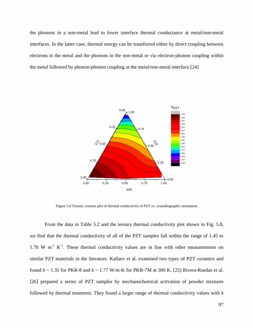
97
the phonons in a non-metal lead to lower interface thermal conductance at metal/non-metal
interfaces. In the latter case, thermal energy can be transferred either by direct coupling between
electrons in the metal and the phonons in the non-metal or via electron-phonon coupling within
the metal followed by phonon-phonon coupling at the metal/non-metal interface.[24]
0.00 0.25 0.50 0.75 1.00
0.00
0.25
0.50
0.75
1.000.00
0.25
0.50
0.75
1.00
kPZT
110
111
100
1.450
1.467
1.483
1.500
1.517
1.533
1.550
1.567
1.583
1.600
1.617
1.633
1.650
1.667
1.683
1.700
Figure 5.8 Ternary contour plot of thermal conductivity of PZT vs. crystallographic orientation
From the data in Table 5.2 and the ternary thermal conductivity plot shown in Fig. 5.8,
we find that the thermal conductivity of all of the PZT samples fall within the range of 1.45 to
1.70 W m-1
K-1
. These thermal conductivity values are in line with other measurements on
similar PZT materials in the literature. Kallaev et al. examined two types of PZT ceramics and
found k ~ 1.35 for PKR-8 and k ~ 1.77 W/m-K for PKR-7M at 300 K. [25] Rivera-Ruedas et al.
[26] prepared a series of PZT samples by mechanochemical activation of powder mixtures
followed by thermal treatment. They found a larger range of thermal conductivity values with k

98
between 0.55 and 2.1 W/m-K at room temperature, and they observed no obvious trends in
thermal conductivity with the composition of the PZT or Pb oxide source, and they attributed the
range of thermal conductivity values to differences in microstructure and porosity. A variety of
other crystalline perovskite ferroelectric materials, including NaNbO3 and Pb(Mg0.33Nb0.67)O3
exhibit similar low thermal conductivity values in the 1 – 3 W/m-K range, while others (e.g.
BaTiO3, KNbO3, PbTiO3, and KTaO3) have slightly larger conductivity in the range of 3-15
W/m-K at room temperature. [27, 28]
While the absolute error in the thermal conductivity values is estimated to be ~15%, the
relative uncertainty between the samples should be considerably less. For example, much of the
absolute error is a result of uncertainties in the Al and Pt film properties, and any errors in these
values will affect all of the samples in the same manner (the Al films were evaporated on all of
the samples simultaneously in one run, so we expect that the Al films on different samples will
have nearly identical thickness). Finally, the small spread in results we obtain on samples with
similar crystal orientations indicates the precision of our measurements.
However, we do observe that there is a ranking of the thermal conductivity with respect
to the crystal orientation. The thermal conductivities of the samples that predominantly contain
(111) are slightly greater than for the samples containing (100), which in turn, are greater than
the (110) samples. The origin of this trend in thermal conductivity is unclear. One possible
reason is the anisotropy of the rhombohedral lattice. If the thermal conductivity is significantly
greater in a particular crystallographic direction, it could cause films of different textures to
exhibit different average thermal conductivities. To confirm this hypothesis, it is necessary to
infer the principal thermal conductivities from the textured films and show they conform to the
rhombohedral symmetry constraint, k11 ~ k22 < k33. To do this, we assumed that the measured
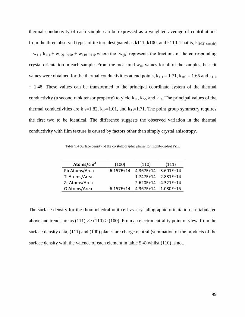
99
thermal conductivity of each sample can be expressed as a weighted average of contributions
from the three observed types of texture designated as k111, k100, and k110. That is, k(PZT, sample)
= w111 k111,+ w100 k100 + w110 k110 where the ‘wijk’ represents the fractions of the corresponding
crystal orientation in each sample. From the measured wijk values for all of the samples, best fit
values were obtained for the thermal conductivities at end points, k111 = 1.71, k100 = 1.65 and k110
= 1.48. These values can be transformed to the principal coordinate system of the thermal
conductivity (a second rank tensor property) to yield k11, k22, and k33. The principal values of the
thermal conductivities are k11=1.82, k22=1.01, and k33=1.71. The point group symmetry requires
the first two to be identical. The difference suggests the observed variation in the thermal
conductivity with film texture is caused by factors other than simply crystal anisotropy.
Table 5.4 Surface density of the crystallographic planes for rhombohedral PZT.
Atoms/cm2 (100) (110) (111)
Pb Atoms/Area 6.157E+14 4.367E+14 3.601E+14 Ti Atoms/Area 1.747E+14 2.881E+14 Zr Atoms/Area 2.620E+14 4.321E+14 O Atoms/Area 6.157E+14 4.367E+14 1.080E+15
The surface density for the rhombohedral unit cell vs. crystallographic orientation are tabulated
above and trends are as (111) >> (110) > (100). From an electroneutrality point of view, from the
surface density data, (111) and (100) planes are charge neutral (summation of the products of the
surface density with the valence of each element in table 5.4) whilst (110) is not.
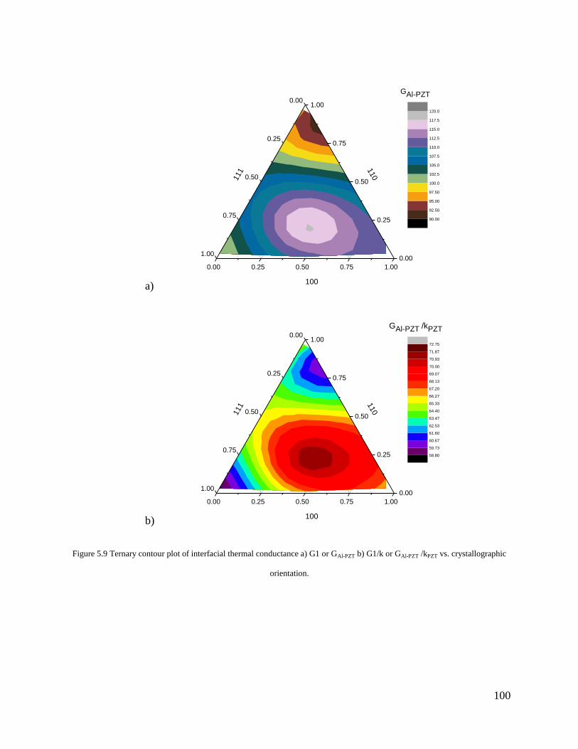
100
a)
0.00 0.25 0.50 0.75 1.00
0.00
0.25
0.50
0.75
1.000.00
0.25
0.50
0.75
1.00
110
111
100
90.00
92.50
95.00
97.50
100.0
102.5
105.0
107.5
110.0
112.5
115.0
117.5
120.0
GAl-PZT
b)
0.00 0.25 0.50 0.75 1.00
0.00
0.25
0.50
0.75
1.000.00
0.25
0.50
0.75
1.00
GAl-PZT /kPZT
110
111
100
58.80
59.73
60.67
61.60
62.53
63.47
64.40
65.33
66.27
67.20
68.13
69.07
70.00
70.93
71.87
72.75
Figure 5.9 Ternary contour plot of interfacial thermal conductance a) G1 or GAl-PZT b) G1/k or GAl-PZT /kPZT vs. crystallographic
orientation.
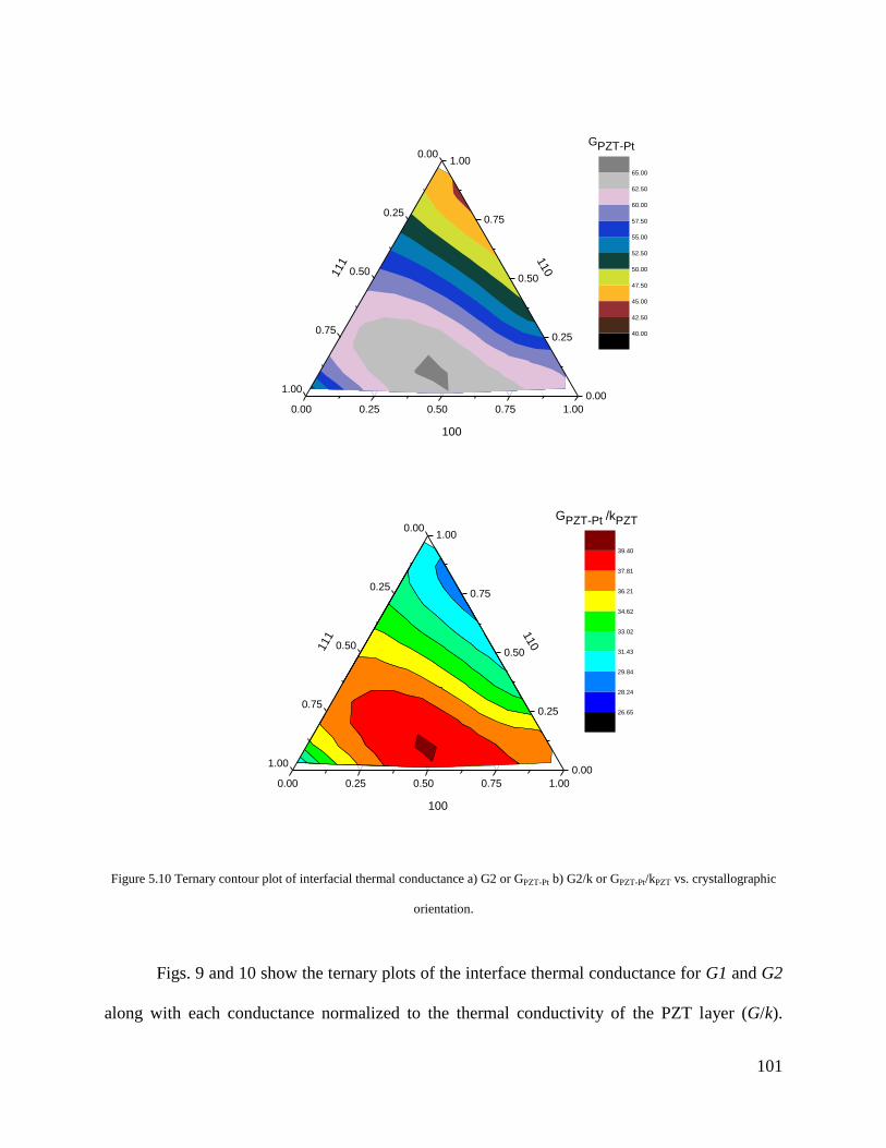
101
0.00 0.25 0.50 0.75 1.00
0.00
0.25
0.50
0.75
1.000.00
0.25
0.50
0.75
1.00
GPZT-Pt
110
111
100
40.00
42.50
45.00
47.50
50.00
52.50
55.00
57.50
60.00
62.50
65.00
0.00 0.25 0.50 0.75 1.00
0.00
0.25
0.50
0.75
1.000.00
0.25
0.50
0.75
1.00
GPZT-Pt /kPZT
110
111
100
26.65
28.24
29.84
31.43
33.02
34.62
36.21
37.81
39.40
Figure 5.10 Ternary contour plot of interfacial thermal conductance a) G2 or GPZT-Pt b) G2/k or GPZT-Pt/kPZT vs. crystallographic
orientation.
Figs. 9 and 10 show the ternary plots of the interface thermal conductance for G1 and G2
along with each conductance normalized to the thermal conductivity of the PZT layer (G/k).

102
From the G1 ternary plot, all measurements fall within a range of 90-120 MW m-2
K-1
, with nine
of the twelve samples having magnitudes between 100 and 110 MW m-2
K-1
. The largest
conductance values, albeit by a small yet consistent margin, are for samples with significant
fraction of (100), with the largest measurement for a roughly 40/20/40 mixture of (100), (110),
and (111) orientations. The smallest G1 values are for samples with large fractions of (111). For
the G2 ternary plot, roughly even mixtures of (111) and (100) give the largest conductances,
while samples with large fractions of (100) are also high, and samples containing over 90%
fractions of (110) have the lowest conductances. Thus G1 and G2 trend slightly as (100) > (111)
> (110); while G1/k and G2/k trend as (100) > (110) ~ (111).
If PbO [1, 9], Ti-rich PZT (~PbTiO3) [4, 8] and ZrO2 [9] are seeding the (100) texture,
then G2 should decrease with an increase in (100), however, this decrease in G2 would be small
because any oxide layer here would be thin. The thermal conductivity of the elements at the
PZT-Pt interface trend as: Pt > Pb >> Zr > Ti >>> O. From surface density calculations, (100)
have a higher Pb surface density than (111) and (110) and this may enhance G2. The segregation
of Ti at the PZT-Pt interface, as seen in the (111) sample’s EDS results, has been observed
earlier[29] where it was attributed to the Ti flow (and Zr flow away) to the growth interface
where heterogeneous nucleation and growth of the crystalline PZT phase occurs. As per binary
phase diagrams of Pt-Pb, Pt-Zr and Pt-Ti[30], only Ti and Zr can dissolve in Pt whilst all three,
Pb, Ti and Zr, will form intermetallics.
GI-XRD results confirmed standard XRD results for all textured films except for the
texturing mixture films 64, 4D, 68 and 7D. All of these films have some pyrochlore
Pb2(Zr,Ti)2O6 (JCPDS 26-0142). However, samples 68 and 7D are mixtures of 40-50% of (100)
with (111) with also show the presence of Pt-Ti alloy (JCPDS 27-1310). These samples also
103
have the largest interface conductances. Sample 4D has a lower G2 than 64, and that may be due
to higher amount of pyrochlore in the former. With regards to both G1 and G2 having similar
general trends, this could suggest that the anisotropy within the PZT films may be the reason for
the slight dependence of G on the crystallographic orientation.
In addition to the textured PZT films, we also examined a 1 micron thick amorphous
sample. In this thick sample, the heat pulses from the laser do not penetrate beyond the PZT
layer and therefore there are only two unknown parameters, G1 and kPZT. As one would expect,
the thermal conductivity of this amorphous sample is considerably smaller than the conductivity
for the crystalline films, as k is 0.53 W m-1
K-1
. Interestingly, despite the significant change in
the crystal structure of the PZT film, and, subsequently, the film thermal conductivity, the
interface thermal conductance, G1, was found to be similar to previous measurements at 100
MW m-2
K-1
. One possible reason for the lack of change in G1 with the large change in PZT film
structure could be that this interface thermal conductance is controlled by the electron-phonon
coupling within the aluminum.
Conclusion
In this article, we report the use of a non-contact optical technique called Time-Domain
Thermoreflectance to examine the thermal conductivity and interface thermal conductance for a
series of textured PZT samples grown by a sol-gel process. We find that the thermal conductivity
of the PZT films ranges from 1.45 to 1.70 W m-1
K-1
and has a slight dependence on film texture.
The interface thermal conductance at Al/PZT and Pt/PZT interfaces also show a similar
dependence on crystal orientation. While the origin of these trends is not clear, one possible

104
explanation is that the anisotropy within the PZT films is responsible for the observed
dependence of thermal conductivity and interface thermal conductance.
Acknowledgements: The authors gratefully acknowledge the financial support from Air Force
Office of Scientific Research (AFOSR) through the Young Investigator Program and Office
of Naval Research through CEHMS seed program. We are also greatly indebted to Reema Gupta
for assistance with GI-XRD indexing, Shashank Gupta for valuable discussions, Charles Farley
for the FTIR characterization work conducted at Department of Geosciences at Virginia Tech,
Holger Cordes of Bruker-AXS for GI-XRD, Ashok Kumar for the Raman work conducted at
University of Puerto Rico’s Speclab, Deepam Maurya and Chris Winkler for the TEM
micrographs and Jerry Hunter of Nanoscale Characterization and Fabrication Lab at Virginia
Tech for the XPS analysis.
References
[1] Chen S-Y, Chen IW. Temperature–Time Texture Transition of Pb(Zr1−xTix)O3 Thin
Films: II, Heat Treatment and Compositional Effects. Journal of the American Ceramic Society
1994;77:2337.
[2] Daniel M. Potrepka GRF, Luz M. Sanchez and Ronald G. Polcawich. Pt/TiO2 Growth
Templates for Enhanced PZT films and MEMS Devices. MRS Proceedings 2011.;1299:s02.
[3] Huang Z, Zhang Q, Whatmore RW. The Role of an Intermetallic Phase on the
Crystallization of Lead Zirconate Titanate in Sol–gel Process. Journal of Materials Science
Letters 1998;17:1157.
[4] L.M. Sanchez DMP, G.R. Fox, I. Takeuchi and R.G. Polcawich. Improving PZT Thin
Film Texture Through Pt Metallization and Seed Layers. MRS Proceedings 2011;1299:s04.
[5] Nittala K, Mhin S, Dunnigan KM, Robinson DS, Ihlefeld JF, Kotula PG, Brennecka GL,
Jones JL. Phase and texture evolution in solution deposited lead zirconate titanate thin films:

105
Formation and role of the Pt[sub 3]Pb intermetallic phase. Journal of Applied Physics
2013;113:244101.
[6] Norga GJ, Fé L, Vasiliu F, Fompeyrine J, Locquet JP, Van der Biest O. Orientation
selection in functional oxide thin films. Journal of the European Ceramic Society 2004;24:969.
[7] Reaney I, Taylor D, Brooks K. Ferroelectric PZT Thin Films by Sol-Gel Deposition.
Journal of Sol-Gel Science and Technology 1998;13:813.
[8] Tyholdt F, Calame F, Prume K, Ræder H, Muralt P. Chemically derived seeding layer for
100-textured PZT thin films. J Electroceram 2007;19:311.
[9] Zhu C, Chentao Y, Sheng W, Bangchao Y. The effects of the PbO content and seeding
layers upon the microstructure and orientation of sol-gel derived PZT films. J Mater Sci: Mater
Electron 2006;17:51.
[10] Varghese R, Williams M, Gupta S, Priya S. Temperature-time transformation diagram for
Pb(Zr,Ti)O[sub 3] thin films. Journal of Applied Physics 2011;110:014109.
[11] Hopkins PE, Beechem T, Duda JC, Hattar K, Ihlefeld JF, Rodriguez MA, Piekos ES.
Influence of anisotropy on thermal boundary conductance at solid interfaces. Physical Review B
2011;84.
[12] Costescu RM, Wall MA, Cahill DG. Thermal conductance of epitaxial interfaces.
Physical Review B 2003;67:054302.
[13] Duda JC, Kimmer CJ, Soffa WA, Zhou XW, Jones RE, Hopkins PE. Influence of
crystallographic orientation and anisotropy on Kapitza conductance via classical molecular
dynamics simulations. Journal of Applied Physics 2012;112.
[14] Cahill DG, Ford WK, Goodson KE, Mahan GD, Majumdar A, Maris HJ, Merlin R,
Phillpot SR. Nanoscale thermal transport. Journal of Applied Physics 2003;93:793.
[15] Cahill DG, Goodson K, Majumdar A. Thermometry and thermal transport in
micro/nanoscale solid-state devices and structures. Journal of Heat Transfer-Transactions of the
Asme 2002;124:223.
[16] Huxtable S. Time-Domain Thermoreflectance Measurements for Thermal Property
Characterization of Nanostructures. In: Haight R, Ross FM, Hannon JB, editors. Handbook of
Instrumentation and Techniques for Semiconductor Nanostructure Characterization, vol. 2.
Hackensack, NJ: World Scientific Publishing Co. , 2012. p.587.
[17] Wang Y, Park J, Koh YK, Cahill DG. Thermoreflectance of metal transducers for time-
domain thermoreflectance. Journal of Applied Physics 2010;108:043507.
[18] Cahill DG. Analysis of heat flow in layered structures for time-domain
thermoreflectance. Rev. Sci. Instrum. 2004;75:5119.
[19] Feldman A. Algorithm for solutions of the thermal diffusion equation in a stratified
medium with a modulated heating source. High Temp.-High Press. 1999;31:293.
[20] Lang SB, Zhu WM, Ye ZG. Specific heat of ferroelectric Pb(Zr1-xTix)O-3 ceramics
across the morphotropic phase boundary. Journal of Applied Physics 2012;111.
[21] Gundrum BC, Cahill DG, Averback RS. Thermal conductance of metal-metal interfaces.
Physical Review B 2005;72:245426.
[22] Souza Filho AG, Lima KCV, Ayala AP, Guedes I, Freire PTC, Melo FEA, Mendes Filho
J, Araújo EB, Eiras JA. Raman scattering study of the PbZr_1-xTi_xO_3 system:
Rhombohedral-monoclinic-tetragonal phase transitions. Physical Review B 2002;66:132107.
[23] Lyeo HK, Cahill DG. Thermal conductance of interfaces between highly dissimilar
materials. Physical Review B 2006;73:144301.
106
[24] Majumdar A, Reddy P. Role of electron-phonon coupling in thermal conductance of
metal-nonmetal interfaces. Applied Physics Letters 2004;84:4768.
[25] Kallaev SN, Gadzhiev GG, Kamilov IK, Ornarov ZM, Sadykov SA, Reznichenko LA.
Thermal properties of PZT-based ferroelectric ceramics. Physics of the Solid State
2006;48:1169.
[26] Rivera-Ruedas G, Ramirez-Lopez LM, de Jesus FS, Bolarin-Miro A, Munoz-Saldana J,
Yanez-Limon JM. Thermal Characterization of PZT Ceramics Obtained by Mechanically
Activated Mixed Oxides Using Different Pb Sources. International Journal of Thermophysics
2012;33:2366.
[27] Zhu DM, Han PD. Thermal conductivity and electromechanical property of single-crystal
lead magnesium niobate titanate. Applied Physics Letters 1999;75:3868.
[28] Tachibana M, Kolodiazhnyi T, Takayama-Muromachi E. Thermal conductivity of
perovskite ferroelectrics. Applied Physics Letters 2008;93.
[29] Muralt P. Recent Progress in Materials Issues for Piezoelectric MEMS. Journal of the
American Ceramic Society 2008;91:1385.
[30] Massalski TBOHASMI. Binary alloy phase diagrams. Materials Park, Ohio: ASM
International, 1990.

107
Chapter 6
Piezocap: a MEMS Scalable Non Dimensional Decoupled
Vibration Energy Harvester
R. Varghese1, Justin Farmer
1, Mohan Sanghadasa
2, and Shashank Priya
1
1Center for Energy Harvesting Materials and Systems (CEHMS), Bio-inspired Materials and Devices Laboratory (BMDL), Virginia Tech,
Blacksburg, VA 24061
2Weapons Sciences Directorate, U.S. Army Research, Development, and Engineering Command, Redstone Arsenal, AL 35898
Abstract
We describe a novel concept towards the development of a MEMS scalable low frequency non-
cantilever type broadband piezoelectric energy harvester with active tunability. This structure
decouples the energy harvesting component of the device from the resonant vibration
component. In doing so, each component can be tailored for maximum efficiency, better
scalability and versatility. We did so by using a levitated magnet between two magnets which are
in turn attached to two peripherally clamped piezoelectric macro fiber composite strips. The
center magnet transfers the source vibration into the device and the outer magnets flex the macro
fiber composites. The device incorporates commercial d33-mode P1 type macro fiber composite
on one side and a d31-mode P2 type macro fiber composite on the other. We obtained 1.259 μW
(1.01 Voc) @ matching load of 225 kΩ and 1.309 μW (0.210Voc) @ 15k for P1 and P2 type
harvesters respectively at 460Hz and 1g acceleration. To demonstrate active tunability, we
moved to a 2 magnet system with each magnet on the two piezoelectric harvesters and we
analyzed the performance against the distance between the magnet + piezo harvester pairs. We

108
discovered that at a certain threshold distance, the natural frequency of the 2 piezomagnetoelastic
systems equal that of a single piezoelectric harvester with an inertial mass equivalent to that of
the magnet. Below that threshold distance, the 2 piezoelectric harvesters also are observed to be
in synch. We obtained 0.133 μW (0.014 Voc) and 0.559 μW (0.029 Voc) from Top and Bottom
harvesters and 3.717 μW (0.119 Voc) and 2.027 μW (0.080 Voc) from Top and Bottom harvesters
bonded to Nickel @ matching load of 1500Ω at 626Hz and 1647Hz respectively and 0.3g
acceleration. With this work, we therefore demonstrate that with the use of magnets, the
dimensionality of harvester’s resonant frequency is eliminated and tunability of such of system is
purely based on the magnetic force between the magnets.
Keywords: Nonlinear energy harvesting, Piezoelectric, Piezomagnetoelastic, magnetic stiffness,
piezo stiffness, linear stiffness, non linear stiffness
Introduction
At the MEMS scale, piezoelectric transduction is the preferred approach in vibration energy
harvesting[1]. Traditionally, MEMS based vibrational harvesters utilize a piezoelectric layer over
a cantilever structure with tip mass (fixed-free beam configuration). The vibration from the
external source is transferred to the cantilever which in turns strains the piezoelectric layer and
generates an electric charge. Therefore, the energy harvesting capability is limited by the
cantilever area where non-zero strain is present and optimum performance is limited to the
narrow region in the vicinity of resonance frequency.
Optimal performance of vibration energy harvesters occurs when their resonance frequency is
tuned to that of the source resonance frequency. Resonance frequency of such vibration energy
109
harvesters is controlled by the dimensions of the device – that is, the mass, length, width and
thickness of the vibrating structure. Tunability of this resonance frequency by dimensional
variation is complex and usually inconvenient but nondimensional approaches using magnets,
load, electrical bias, etc. have been integrated successfully[2]. But what if there is an approach
that is nondimensional whilst also decoupling the resonant condition from harvester’s natural
frequency. That is, can we create an energy harvester which performs best at a frequency away
from the resonant frequency of its piezoelectric elements?
We demonstrate here a new MEMS scalable device, termed as PiezoCap, which separates
the vibration transfer component from the energy harvesting component. That is, one section of
this device, a central magnet, will transfer the source vibration into the device and then that
vibration is transferred to piezoelectric transducer element. In doing so, the resonance of the
transfer element can be tuned to the source frequency and the transducer element can be
designed for maximum energy harvesting capability. Such separation of duties in an energy
harvester will lead to realization of low frequency micro scale vibrational devices with maximum
piezoelectric area. Unlike cantilever based MEMS devices, the resonance of the device is easily
modified by changing the magnetic stiffness without changing the dimensions of the
piezoelectric transducer element. We are also able to combine both d33 and d31 mode energy
harvesting on the same footprint. For proof of concept, we built a magnetically levitated transfer
element coupled to piezoelectric macro fiber composites (MFC) for transduction. Mann et.al[3]
measured the spring force of a 3 magnet system similar to our 1st prototype and arrived at a least
squares fitted spring force relationship that related the displacement of a center magnet ‘x’
(analogous to the displacement of our piezo harvesters) with the spacing between magnets ‘D’.
2 3 3
1 2 3 3 3( ) (2 4 6 ) 2F x D D x x kx k x where αi are coefficients of the fit (1)
110
We extended this decoupled harvester concept for active tunability and nondimensionality of the
resonant frequency by using a simpler 2 magnet+piezoelectric pair, that is, a dual
piezomagnetoelastic system. Unlike, the tuning magnet on a fixed support approach by Challa
et.al[4], this system is closer to the magnetic oscillator configuration by Tang et.al[5]. Stanton
et.al[6] used a piezo cantilever with a magnetic inertial mass with 2 perpendicular fixed magnets
that moved along the length of the cantilever to induce hardening and softening stiffness.
However, we are using a fixed-fixed beam piezoelectric actuator as the oscillating support for the
magnets and the magnets are always in repulsion. Repulsion mode has been found by Tang et.al.
to have the best harvesting voltage and bandwidth performance especially when operated near
the monostable-bistable transition zone of the intermagnetic spacing[7]. They also show that in
attractive mode, the resonance increases and in repulsion mode, the resonance decreases in
comparison to a linear non-magnetic piezo actuator configuration.
As can be determined from the name, PiezoCap is designed to be utilized as an
encapsulating package for microelectronics chips. In the MEMS scale, unlike traditional
cantilever based piezo methodologies[8], the PiezoCap based harvesters will provide larger piezo
area as the latter has been moved off the mechanically resonant beam. In doing so, we are not
limited to deposited films and their related limitations of throughput and film stress, but can
utilize ceramic or single crystal piezoelectric elements.
Experimental Details
Prototype 1
Piezoelectric macro fiber composites (MFC’s), M-2814-P1 (d33 mode) and M-2814-P2 (d31
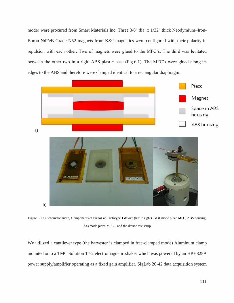
111
mode) were procured from Smart Materials Inc. Three 3/8" dia. x 1/32" thick Neodymium–Iron-
Boron NdFeB Grade N52 magnets from K&J magnetics were configured with their polarity in
repulsion with each other. Two of magnets were glued to the MFC’s. The third was levitated
between the other two in a rigid ABS plastic base (Fig.6.1). The MFC’s were glued along its
edges to the ABS and therefore were clamped identical to a rectangular diaphragm.
a)
b)
Figure 6.1 a) Schematic and b) Components of PiezoCap Prototype 1 device (left to right) – d31 mode piezo MFC, ABS housing,
d33 mode piezo MFC – and the device test setup
We utilized a cantilever type (the harvester is clamped in free-clamped mode) Aluminum clamp
mounted onto a TMC Solution TJ-2 electromagnetic shaker which was powered by an HP 6825A
power supply/amplifier operating as a fixed gain amplifier. SigLab 20-42 data acquisition system
112
with four input channels and two output channels is used for the Voltage frequency response
function (FRF) measurements. The reference acceleration was measured at the clamp using a
accelerometer (Piezotronics Inc. model # U352C67). Voltage generated by the harvester and the
power loading curves were generated by placing a digital IET Labs load resistor in series with
the harvesters. The output signal from the accelerometer was conditioned using a charge
amplifier (Piezotronics Inc.). The velocity at the tip of cantilever beam was measured using a
digital vibrometer (Polytec OFV 353). Polytec 5000 controller was used to generate input signals
to the seismic shaker to create vibration and also to capture the output signals from
accelerometer and vibrometer. The velocity FRF’s for each piezomagnetoelastic harvester was
measured by clamping each of them facing the laser head.
Prototype 2
Rectangular d31 mode piezoelectric actuators, called Quikpaks, model # QP16n from Midé were
cut to the square shape at the piezo end. ABS plastic base of 25mm height was 3D printed and
used as the housing to levitate the center magnet and clamp the piezo harvesters by their corners
on opposing faces. A new clamp in line with shaker motion eliminated the cantilever clamping
induced resonant peaks of Prototype 1. 2 NdFeB magnets of 1/8” diameter x 1/32” height was
placed on each piezo actuator as shown below. The dual magnet configuration was chosen to
improve the strain capability of each PiezoCap. The center NdFeB magnet was a 1/4” diameter x
1/8” height.

113
a)
b) c)
Figure 6.2 a) Schematic and b) Components of PiezoCap Prototype 2 – 2 Quikpaks spaced apart by ABS housing and held by
clear plastic cylinders and the device test setup
Prototype 3
Quikpaks from Prototype 2 was reused for this prototype. The resonance frequency was

114
measured by laser Doppler Vibrometry of the topmost Quikpak in the device. Understandably,
due to the clamp and shaker, the velocity FRF’s of only the top piezomagnetoelastic harvester
could only be measured. However, generated voltage was collected from both top and bottom
harvesters.
a)
b)
Figure 6.3 a) Schematic and b) Components of PiezoCap Prototype 3 – 2 Quikpaks spaced apart by and held by Brass washers
and the device test setup
0.125”, 0.063”. 0.032” and 0.016” thickness brass washers were used in varying combinations to
achieve the variable spacing between the 2 magnet + harvesters pairs. Velocity and Voltage FRF

115
data was collected for 3 device configurations: a) with 2 different sizes of NdFeB magnets - ¼”
diameter x 1/8” thickness and ¼” x 3/16” – and b) with ¼’’x1/8’’magnets with a 5mils Nickel
201 shim bonded to the Quikpaks. The ¼’’x1/8’’ and ¼” x 3/16” magnets when used as an
inertial mass weighed in at 0.75gms and 1.13gms respectively. The Nickel is a neutral axis
modifier in that it moves the neutral axis of the composite structure into the nickel. Doing so will
ensure that the stresses generated across the piezo thickness are of the same sign for both upward
and downward displacement and therefore do not cancel each other out.
Results and Discussion
Prototype 1
The clamping in a cantilever fashion produces stray resonance peaks from clamp[9] and the
cantilever bending of the device. The Velocity and Voltage FRF’s demonstrate that the
fundamental resonance of the system is due to the piezomagnetoelastic transduction. As the
Smart Materials macro fiber composite harvesters were used as-is (neutral axis in piezo layer),
their energy harvesting performance was limited to 1.259 μW (1.01 Voc) @ matching load of 225
kΩ and 1.309 μW (0.210Voc) @ 15 kΩ for P1 and P2 type harvesters respectively at 460Hz and
1g acceleration.

116
a)
200 400 600 800 1000 1200 1400
0.0000
0.0005
0.0010
0.0015
0.0020
0.0025
0.0030
0.0035
0.0040
0.0045
Clamp
2nd mode
of cantilever type
device clamping
1st mode
of cantilever type
device clamping
Velo
city F
RF
( m
/s /
(m
/s²)
)
Frequency (Hz)
p2
p1PiezoCap
b)
200 400 600 800 1000 1200 1400-40
-30
-20
-10
0
10
20
30
Voltage F
RF
(V
/V,d
B)
Frequency (Hz)
P2
P1
Clamp
2nd mode
of cantilever type
device clamping
1st mode
of cantilever type
device clamping
PiezoCap
Figure 6.4 a) Velocity FRF and b) Voltage FRF for Prototype 1

117
a)
100k 215k 250k 400k 1M 3M 5M 15M0.1
0.2
0.3
0.4
0.5
0.6
0.7
0.8
0.9
1.0 Voltage
Power
Resistance (Ohm)
Voltage (
Volt)
0.0
0.2
0.4
0.6
0.8
1.0
1.2
1.4
Pow
er
(W
att
)
P1 harvester
b)
5k 7k 9k 9.5k 10k 20k 40k 100k 300k0.00
0.02
0.04
0.06
0.08
0.10
0.12
0.14
0.16
0.18
0.20
P2 harvester
Voltage
Power
Resistance (Ohm)
Voltage (
Volt)
0.0
0.2
0.4
0.6
0.8
1.0
1.2
1.4
Pow
er
(W
att
)
Figure 6.5 Voltage and Power loading curves for a) P1 d33 MFC and b) P2 d31 MFC
Prototype 2
We used edge clamping to increase area under strain in the piezo harvesters. To obtain low

118
resonant frequency, we used a taller ABS housing that provided a 15mm gap between the
magnets. However, we could not obtain a single resonant frequency for the piezomagnetoelastic
transduction. However, the resonances of the levitated 3 magnet system and the Quikpak are
separately visible. Therefore, we realized that we need larger magnets in proximity to achieve
high piezomagnetoelastic performance.
0 200 400 600 800 100012001400160018002000
0.000
0.002
0.004
0.006
0.008
0.010
0.012
0.014
0.016
0.018
0.020
Velo
city F
RF
( m
/s /
(m
/s²)
)
Frequency (Hz)
1/8x1/32 on piezo + 1/4x1/16
1/8x1/32 + 1/4x1/16
Maglev fr
Piezo fr
Figure 6.6 Separation of fundamental resonances in Prototype 2: bottom curve with magnets without piezo and top with magnets
on piezo
Prototype 3
The change in resonance frequency vs. the gap between the 2 piezomagnetoelastic harvesters
using brass washers are shown below. The fundamental resonance is observed to follow a bowl
profile with spacing between the magnets for all the 3 harvester configurations of 0.75gm
magnets, 1.13magnets and Ni+0.75gm magnets. The minimum occurs expectedly at different

119
threshold spacing for each of these configurations. This minimum resonant frequency matches
that of a Quikpak with a single magnet as inertial mass. The frequency shift from this minimum
follows a zigzag pattern. When the two piezomagnetoelastic harvesters are brought closer from
the tens of mm’s distance, the repulsion magnetic fields will increase the stiffness of the system
and then as the magnetic forces balances out the piezo stiffness force, the resonance reaches the
minimum.
Magnet
Magnet
Magnet
Magnet
Magnet
kPiezo
kPiezo
kPiezo
kPiezo
kmag
kmag
kmag
Figure 6.7 The spring force diagrams for Prototype 1 on left and 2 on right
This phenomenon can be explained by the effective spring constant for springs in series (as
shown in above figure for Prototype 1 and 3):

120
1
1 1 1 2
when then
1and
2
piezo mag
eff
mag piezo
piezo mag piezo
piezo mag eff piezo
eff
n
eff
k kk
k k
k k k
k k k k
k
m
(2)
Further decrease at this minimum resonance or threshold distance, the magnetic fields increase
the stiffness back again.
1400 1500 1600 1700 1800 1900 20000.0000
0.0005
0.0010
0.0015
0.0020
0.0025
Velo
city F
RF
(m
/s /
(m
/s²)
)
Frequency (Hz)
2mm
3mm
4mm
5mm
6mm
7mm
8mm
9mm
10mm
10mm
11mm
12mm
13mm
14mm
15mm
16mm
Figure 6.8 The resonant frequency variation with spacing between the magnets for the Nickel neutral axis modified harvester

121
a)
0 2 4 6 8 10 12 14 16
0.632
0.642
0.651
0.660
0.528
0.552
0.576
0.600
0.630
0.720
0.810
0.900
Spacing (mm)
Nickel +0.75gm
No
rma
lize
d F
req
ue
ncy (
Hz/H
z)
1.13gm
EH + tip mass
EH + tip mass
Fundamental Resonance
0.75gm
EH + tip mass
b)
0 2 4 6 8 10 12 14 16
0
25
50
75
0
25
50
75
0
93
186
279
Fre
qu
en
cy c
ha
ng
e (
Hz)
Spacing (mm)
Nickel +0.75gm
1.13gm
0.75gm
Tunability

122
c)
0 2 4 6 8 10 12 14 16
83.2
89.6
96.0
102.4
70
80
90
10050
75
100
125
Spacing (mm)
Nickel +0.75gm
Frequency Bandwidth
3d
B b
an
dw
idth
(H
z)
1.13gm
0.75gm
d)
0 2 4 6 8 10 12 14 16
0.000
0.015
0.030
0.045
0.000
0.023
0.046
0.069
0.000
0.011
0.022
0.033
0.044
Spacing (mm)
Nickel +0.75gm
Vo
lta
ge
diffe
ren
ce
(V
)
1.13gm
Synchronization
0.75gm
Figure 6.9 Variation in a) normalized resonance b) frequency shift c) 3dB bandwidth and d) generated voltage difference for
Prototype 3
123
Interestingly, the 3dB bandwidth decreases linearly with spacing and may be due to increased
non linearity and transition from monostable to bistable potential energy state of the repulsive
magnetic system. The Q (=fr/Δf) ranged from 17-21, 6-9 and 6-12 for the Nickel modified +
0.75gm, 1.13gm and 0.75gm magnet systems respectively. The heavier magnet system had the
least Q factor and the largest bandwidth for operation. Also, as the 2 piezomagnetoelastic
harvesters are brought closer, their generated voltages become closer in value and demonstrate a
possible methodology for synchronization of multiple vibration harvesters. This is especially true
because there is no alignment guide or rod to center 2 magnets directly over each other. With
smaller intermagnetic spacing below a threshold distance, the magnets are now in bistable
configuration and can easily find their mutual potential energy minimum by jumping across the
energy barrier across the 2 potential energy wells[7].
Tang et.al[7] states that the threshold distance is when the spring forces for the repulsive magnets
equates the spring force due to the piezo stiffness. The spring force in the system for ‘x’ amount
of deflection of the piezo harvester is
3
, ,( ) piezo linear mag nonlinear magF x k k x k x (4)
The linear magnetic stiffness term is negative for magnets in repulsion and so the linear term will
eliminate itself by equaling that of the piezo at a certain magnetic spacing ‘D’. When equating
the linear terms to zero, we can get the threshold distance ‘D’ between the magnets as
1/523
2
o
piezo
d mD
k
(5)
where d is a geometrical factor related to the distance between the measurement point and the
harvester free end, µo is the permeability constant 4π x 10-7
N/A2, and m is the magnetic
moment. From the equation, we can see that higher piezo stiffness requires higher magnetic

124
moment for the same D. Below this threshold distance, the magnets are in a bistable state (the
potential energy of the system has a double well with respect to ‘x’) and in a monostable state
above it. This phenomenon might explain the increase in bandwidth with decrease in spacing and
the synchronization of the harvesters.
The linear and nonlinear spring constants for the magnets are proportional to D-5
and D-7
respectively[7]. Therefore with decrease in D, these spring constants will increase considerably
and that too, in opposite directions with the nonlinear term increasing at a slower rate. The linear
magnetic stiffness force is negative and the non-linear term is positive. With decease in D, the
negative component has a softening effect whilst non-linear term has a hardening effect. This
non-linear hardening explains the initial increase in resonance frequency with decrease in D
followed by the linear softening then taking over and decreasing the resonance frequency.
Further decrease in D causes the non-linear hardening force (proportional to x3) overcome the
negative linear softening force. In addition, a bistable state is achieved and the system has to
transition across the energy barrier between the 2 potential wells. Herein lays the crux of the
non-dimensionality aspect of this piezo vibration harvester. Near the threshold distance D, the
magnetic stiffness force is predominant and therefore will determine resonance of the system.
Since the mass of the system is unchanged, the resonance frequency will decrease as observed.
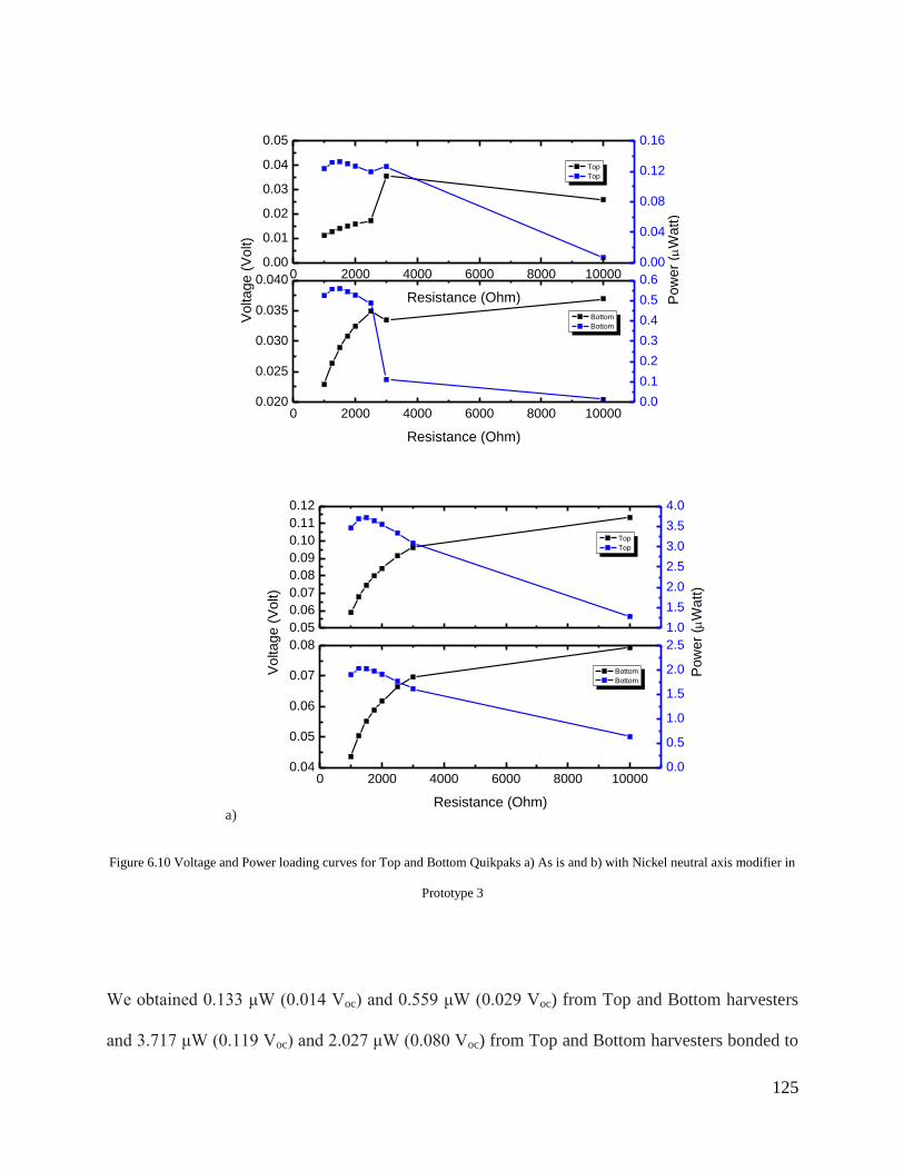
125
0 2000 4000 6000 8000 100000.00
0.01
0.02
0.03
0.04
0.05
Top
Top
Resistance (Ohm)
Voltage (
Volt)
0.00
0.04
0.08
0.12
0.16
0 2000 4000 6000 8000 100000.020
0.025
0.030
0.035
0.040
Bottom
Bottom
Resistance (Ohm)
0.0
0.1
0.2
0.3
0.4
0.5
0.6
Pow
er
(W
att
)
a)
0.05
0.06
0.07
0.08
0.09
0.10
0.11
0.12
Bottom
Bottom
Voltag
e (
Volt)
1.0
1.5
2.0
2.5
3.0
3.5
4.0
Po
we
r (
Wa
tt)
0 2000 4000 6000 8000 100000.04
0.05
0.06
0.07
0.08
Top
Top
Resistance (Ohm)
0.0
0.5
1.0
1.5
2.0
2.5
Figure 6.10 Voltage and Power loading curves for Top and Bottom Quikpaks a) As is and b) with Nickel neutral axis modifier in
Prototype 3
We obtained 0.133 μW (0.014 Voc) and 0.559 μW (0.029 Voc) from Top and Bottom harvesters
and 3.717 μW (0.119 Voc) and 2.027 μW (0.080 Voc) from Top and Bottom harvesters bonded to

126
Nickel @ matching load of 1500Ω at 626Hz and 1647Hz respectively and 0.3g acceleration.
With this piezomagnetoelastic system, we achieved 3.09x higher voltage than that of the piezo
alone with an inertial mass, 4.18x on adding a neutral axis modifier to the piezo harvesters and
finally 5.74x with the neutral axis modifier at the threshold distance.
To fabricate PiezoCap in the MEMS scale, Piezo thin films and electrode patterns will be first
processed onto a Si wafer. This wafer will be thinned from the opposing side to make a ‘micro’
fiber composite – the PiezoCap component. The center magnet will be held in either a PDMS
(made from Si master mold) or micro machined Si housing. After bonding the outer magnet to
each PiezoCap, both PiezoCaps will be attached to the center magnet housing. This MEMS
device will be more immune to air damping than cantilever based MEMS energy harvesters
(which require vacuum packaging). When the source vibration is replaced with an AC magnetic
field, this device can also operate as a Magnetoelectric MEMS harvester. We also envision
PiezoCap as an active energy harvesting package for integrated circuits or other microelectronic
components.
Conclusion
We have demonstrated a novel concept of nondimensionality of resonance of a piezoelectric
vibration energy harvester using magnetic force. Varying the distance between the magnets in
the resultant piezomagnetoelastic devices provide many advantages like active tunability, high
bandwidth and the synchronization of multiple harvesters. At a certain threshold distance
between magnets, the magnetic force balances that due to the piezo stiffness and the resonance
frequency of the system is that of a piezo with an inertial mass equivalent to the mass of the

127
magnet. We have named this device, PiezoCap, as it can be used as an encapsulating energy
harvester in electronic circuit packages. Finally, we have described the process flow to develop
such a device in the MEMS scale.
Acknowledgements: The authors gratefully acknowledge the financial support from Center of
Energy Harvesting and Material Systems (CEHMS).We are also greatly indebted to
Anthony Marin, Eric Baldrighi, Daniel Apo and Nathan Sharpes, our colleagues in CEHMS for
valuable discussions about the experimental setup.
References
[1] Mitcheson PD. Performance limits of the three MEMS inertial energy generator
transduction types. Journal of Micromechanics and Microengineering 2007;17:S211.
[2] Twiefel J, Westermann H. Survey on broadband techniques for vibration energy
harvesting. Journal of Intelligent Material Systems and Structures 2013.
[3] Mann BP, Sims ND. Energy harvesting from the nonlinear oscillations of magnetic
levitation. Journal of Sound and Vibration 2009;319:515.
[4] Challa VR, Prasad M, Shi Y, Fisher FT. A vibration energy harvesting device with
bidirectional resonance frequency tunability. Smart Materials and Structures 2008;17:015035.
[5] Tang L, Yang Y. A nonlinear piezoelectric energy harvester with magnetic oscillator.
Applied Physics Letters 2012;101:094102.
[6] Stanton SC, McGehee CC, Mann BP. Reversible hysteresis for broadband
magnetopiezoelastic energy harvesting. Applied Physics Letters 2009;95:174103.
[7] Tang L, Yang Y, Soh C-K. Improving functionality of vibration energy harvesters using
magnets. Journal of Intelligent Material Systems and Structures 2012;23:1433.
[8] Andò B, Baglio S, Trigona C, Dumas N, Latorre L, Nouet P. Nonlinear mechanism in
MEMS devices for energy harvesting applications. Journal of Micromechanics and
Microengineering 2010;20:125020.
[9] Erturk A, Inman DJ. Piezoelectric Energy Harvesting: Wiley, 2011.

128
Chapter 7
Magnetoelectric Macro Fiber Composite
Ronnie Varghese, 1 Ravindranath Viswan,
2 Donald Leber,
3 Mingkai Mu,
3 Mohan Sanghadasa
4and Shashank
Priya1,*
1Center for Energy Harvesting Materials and Systems (CEHMS), Bio-Inspired Materials and Devices Laboratory (BMDL), Virginia Tech,
Blacksburg, VA 24061, USA 2Materials Science and Engineering Department, Virginia Tech, Blacksburg, VA 24061, USA
3Electrical and Computer Engineering Department, Virginia Tech, Blacksburg, VA 24061, USA 4Weapons Sciences Directorate, U.S. Army Research, Development, and Engineering Command, Redstone Arsenal, AL 35898
Abstract
This paper describes the fabrication and performance results of a magnetoelectric macro fiber
composite (ME MFC). The magnetoelectric composite was fabricated by bonding a
magnetostrictive layer to a piezoelectric layer using novel approach of low temperature transient
liquid phase (LTTLP) bonding. The composite was diced into 150 micron wide fibers and
bonded to a custom designed copper flexible circuit using a spin coated low viscosity room
temperature curing epoxy. ME MFC’s with varying ferrite thicknesses of 0.6mm and 0.5mm
were fabricated and characterized for energy harvesting. The composite with 0.6mm ferrite
thickness achieved an open circuit voltage of 101mV (ME voltage coefficient of 1667
mV/cmOe) and peak power of 1.9nW across 356kΩ matching load at 264Hz .
Keywords: macro fiber composite; low temperature bonding; magnetoelectric composite

129
Introduction
Magnetoelectric (ME) composites have been found promising for sensors, phase shifters, filters,
and tunable transformers. Such devices usually consist of a composite structure that includes a
magnetostrictive phase in contact with a piezoelectric phase. The efficiency of the elastic
coupling between the two phases depends upon the strain transfer occurring at the interface. The
magnetoelectric response can be maximized by improving the interfacial properties in terms of
matching the mechanical impedance between the magnetostrictive and piezoelectric layers[1],[2].
Epoxy bonding has been found to perform better than both a Ag-Si alloy with 600 oC working
temperature and a thin borosilicate with 500-600 oC bonding layers[3]. In ME thin film
composites, the addition of a Pt layer between the piezoelectric film and the magnetostrictive
film has been shown to double the magnitude of ME coefficient [4]. In the case of bulk ME
composites, the addition of an embedded metallic layer has also resulted in improved ME
performance by suppressing interdiffusion between the cofired piezoelectric and
magnetostrictive layers[5]. Building upon these prior findings, we demonstrate here a metallic
bonding process for attaching the piezoelectric and magnetostrictive layer in ME laminate
composites. The constraints on the bonding process included thin dimensions of the interface and
process temperature below the Curie temperature of the magnetostrictive and piezoelectric
layers.
Transient liquid phase (TLP) bonding has been in use for centuries but has recently come to
prominence in aerospace and semiconductor industries for the joining of two metallic
surfaces[6]. The process entails a thin interlayer metal containing a melting point depressant that
melts and fills the voids of the two metal surfaces in contact. This depressant metal diffuses into
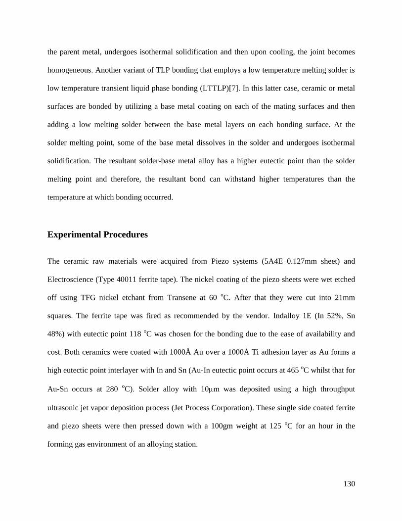
130
the parent metal, undergoes isothermal solidification and then upon cooling, the joint becomes
homogeneous. Another variant of TLP bonding that employs a low temperature melting solder is
low temperature transient liquid phase bonding (LTTLP)[7]. In this latter case, ceramic or metal
surfaces are bonded by utilizing a base metal coating on each of the mating surfaces and then
adding a low melting solder between the base metal layers on each bonding surface. At the
solder melting point, some of the base metal dissolves in the solder and undergoes isothermal
solidification. The resultant solder-base metal alloy has a higher eutectic point than the solder
melting point and therefore, the resultant bond can withstand higher temperatures than the
temperature at which bonding occurred.
Experimental Procedures
The ceramic raw materials were acquired from Piezo systems (5A4E 0.127mm sheet) and
Electroscience (Type 40011 ferrite tape). The nickel coating of the piezo sheets were wet etched
off using TFG nickel etchant from Transene at 60 oC. After that they were cut into 21mm
squares. The ferrite tape was fired as recommended by the vendor. Indalloy 1E (In 52%, Sn
48%) with eutectic point 118 oC was chosen for the bonding due to the ease of availability and
cost. Both ceramics were coated with 1000Å Au over a 1000Å Ti adhesion layer as Au forms a
high eutectic point interlayer with In and Sn (Au-In eutectic point occurs at 465 oC whilst that for
Au-Sn occurs at 280 oC). Solder alloy with 10m was deposited using a high throughput
ultrasonic jet vapor deposition process (Jet Process Corporation). These single side coated ferrite
and piezo sheets were then pressed down with a 100gm weight at 125 oC for an hour in the
forming gas environment of an alloying station.
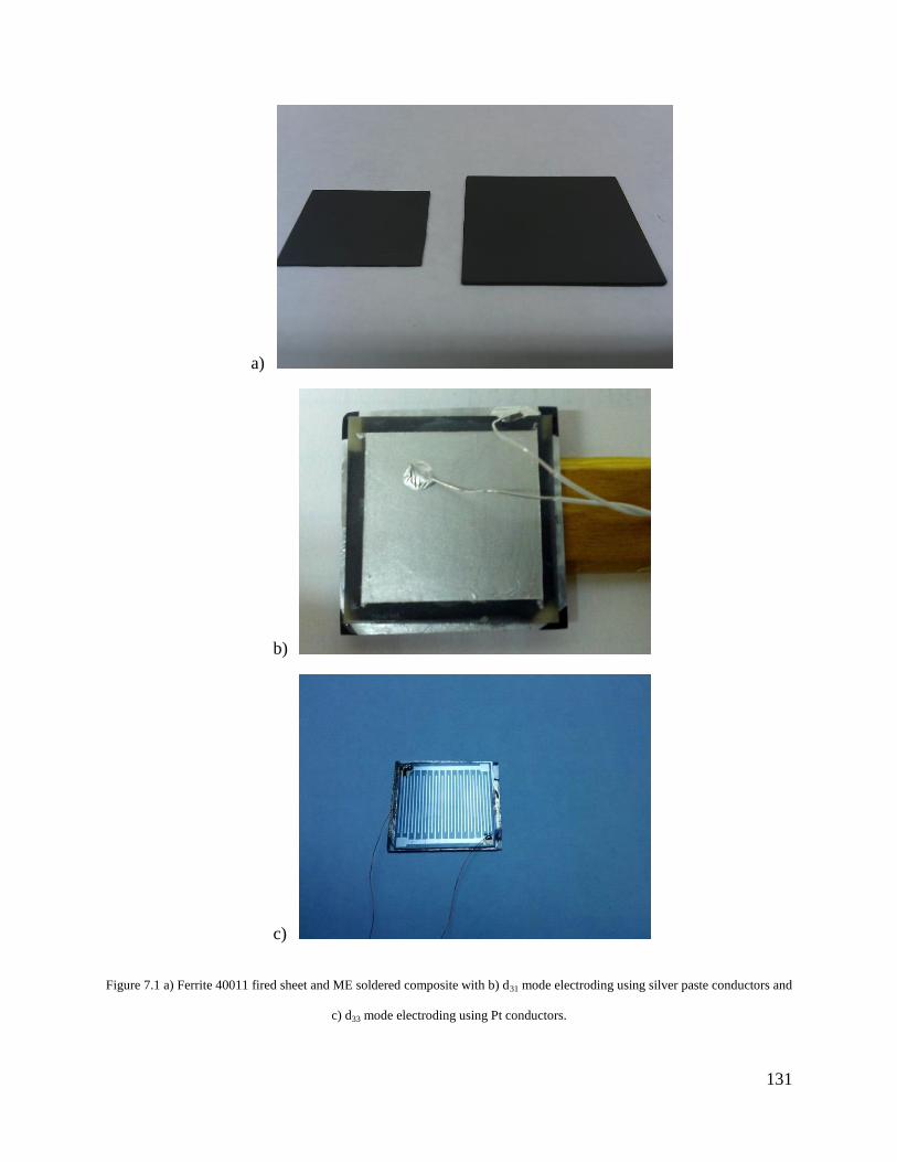
131
a)
b)
c)
Figure 7.1 a) Ferrite 40011 fired sheet and ME soldered composite with b) d31 mode electroding using silver paste conductors and
c) d33 mode electroding using Pt conductors.
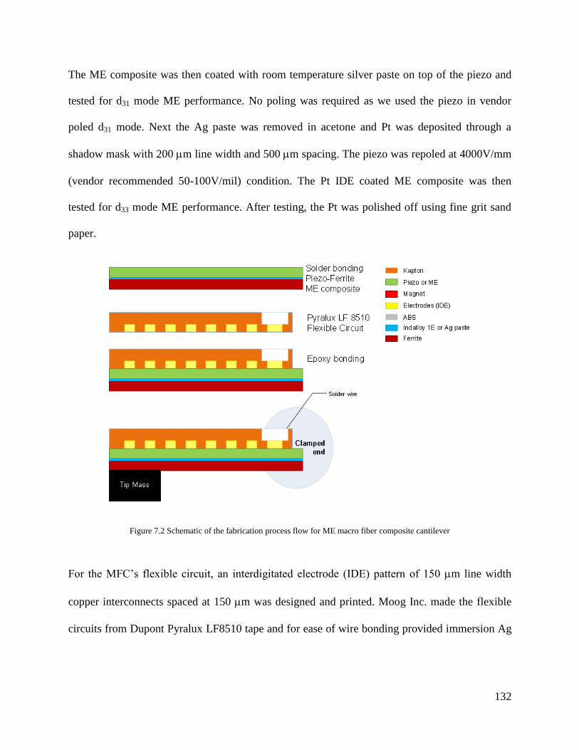
132
The ME composite was then coated with room temperature silver paste on top of the piezo and
tested for d31 mode ME performance. No poling was required as we used the piezo in vendor
poled d31 mode. Next the Ag paste was removed in acetone and Pt was deposited through a
shadow mask with 200 m line width and 500 m spacing. The piezo was repoled at 4000V/mm
(vendor recommended 50-100V/mil) condition. The Pt IDE coated ME composite was then
tested for d33 mode ME performance. After testing, the Pt was polished off using fine grit sand
paper.
Figure 7.2 Schematic of the fabrication process flow for ME macro fiber composite cantilever
For the MFC’s flexible circuit, an interdigitated electrode (IDE) pattern of 150 m line width
copper interconnects spaced at 150 m was designed and printed. Moog Inc. made the flexible
circuits from Dupont Pyralux LF8510 tape and for ease of wire bonding provided immersion Ag

133
finish on the contact pads. The ME composite was diced into 150 m wide fibers with a 3ml
resin blade with 45 m diamond size particles (Semicon Tools, Inc).
a) b)
c) d)
Figure 7.3 a) diced ME composite b) IDE pattern for flexible circuit and c) final ME macro fiber composite (ferrite of 0.5mm on
left and 0.6mm on right) and d) SEM cross section of the ME MFC.
The flexible circuit was spin coated with Extreme 2115 250cP epoxy and vacuum bonded for 12
hours on one side of diced ME composite fibers at room temperature. The MFC was poled at
vendor recommended 4000V/mm condition.
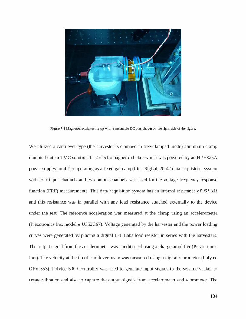
134
Figure 7.4 Magnetoelectric test setup with translatable DC bias shown on the right side of the figure.
We utilized a cantilever type (the harvester is clamped in free-clamped mode) aluminum clamp
mounted onto a TMC solution TJ-2 electromagnetic shaker which was powered by an HP 6825A
power supply/amplifier operating as a fixed gain amplifier. SigLab 20-42 data acquisition system
with four input channels and two output channels was used for the voltage frequency response
function (FRF) measurements. This data acquisition system has an internal resistance of 995 kΩ
and this resistance was in parallel with any load resistance attached externally to the device
under the test. The reference acceleration was measured at the clamp using an accelerometer
(Piezotronics Inc. model # U352C67). Voltage generated by the harvester and the power loading
curves were generated by placing a digital IET Labs load resistor in series with the harvesters.
The output signal from the accelerometer was conditioned using a charge amplifier (Piezotronics
Inc.). The velocity at the tip of cantilever beam was measured using a digital vibrometer (Polytec
OFV 353). Polytec 5000 controller was used to generate input signals to the seismic shaker to
create vibration and also to capture the output signals from accelerometer and vibrometer. The

135
velocity FRF’s for each harvester was measured by clamping each of them and facing the laser
head.
Results and Discussion
The saturation magnetostriction of the ferrite film was measured to be 12ppm and the saturation
occurs at 1767Oe.
0 500 1000 1500 2000 25000
2
4
6
8
10
12
Str
ain
(ppm
)
Field (Oe)
Strain
Figure 7.5 Magnetostriction results for Electroscience Type 40011 ferrite
The resonant frequency and ME voltage coefficients for the 0.5mm thick ferrite ME composites
operating in d31 and d33 modes is shown in Fig. 7.6 and listed in Table 7.1. The applied AC
magnetic field was 1Oe at 1kHz with a saturation DC magnetic bias of 21.9Oe and 27.8Oe
respectively for the 0.5mm and 0.6mm ferrite ME composites. In ME laminates, the first
longitudinal frequency is proportional to the inverse of its length whilst for asymmetric ME
laminates like an ME unimorph, the first bending resonance is lower than that of the longitudinal
and proportional to the inverse of composite length[8] [9]. This explains the low resonance
136
frequencies of the d31 and d33 ME unimorphs prior to their singulation into ME fibers. The ME
voltage coefficients are shifted to the left on the d33 mode vs. the d31mode as the d33 mode
electrode pattern is electrically unidirectional whilst the d31 mode pattern is bidirectional. In
addition, a 2nd
resonance was obtained close to the first. For an unclamped rectangular plate, the
frequency ratio between the 2nd
and 1st modes for length:width ratios[10] of 1, 1.5 and 2.5 are
1.47, 1.07 and 1.53. For a clamped rectangular cantilever, the same ratios are 2.44, 3.56 and
5.21. From the table below, the ratio between modes for our slightly rectangular plates (1 <
length:width ratio < 1.5) range between 1.26-1.63. Unlike the piezo which were diced into 21mm
squares, the square ferrite LTCC tapes were sintered into non-square and slightly rectangular
shapes. For further confirmation, we fabricated a d31 mode piezo similarly sized and shaped as
the ferrite and conducted a frequency impedance analysis. Its 1st resonance was at 59.6 kHz with
a 2nd
mode at 87.6 kHz and 80.6 kHz with a 2nd
mode at 97.8 kHz for d33 and d31 modes
respectively – a mode ratio of 1.47 and 1.21 respectively. A perfectly square resonator is known
to have a whispering gallery effect, that is a single high quality factor resonance due to
combination of both x and y lateral modes[11]. Therefore, the 2nd
peak is due to the 2nd
mode of
a free-free-free-free slightly rectangular plate.

137
a)
0
500
1000
1500
2000
0 5 10 15 20
0
500
1000
1500
2000
ME
coe
ffic
ient
(mV
/cm
Oe
)Frequency (kHz)
d31 0.5mm
Frequency (kHz)
d33
b)
0
500
1000
1500
2000
2500
3000
0 5 10 15 20
0
500
1000
1500
2000
2500
3000
ME
co
eff
icie
nt
(mV
/cm
Oe)
Frequency (kHz)
d310.6mm
Frequency (kHz)
d33
Figure 7.6 Magnetoelectric voltage coefficient results for a) 0.5mm Ferrite and b) 0.6mm Ferrite ME composites operating in d31
and d33 modes.
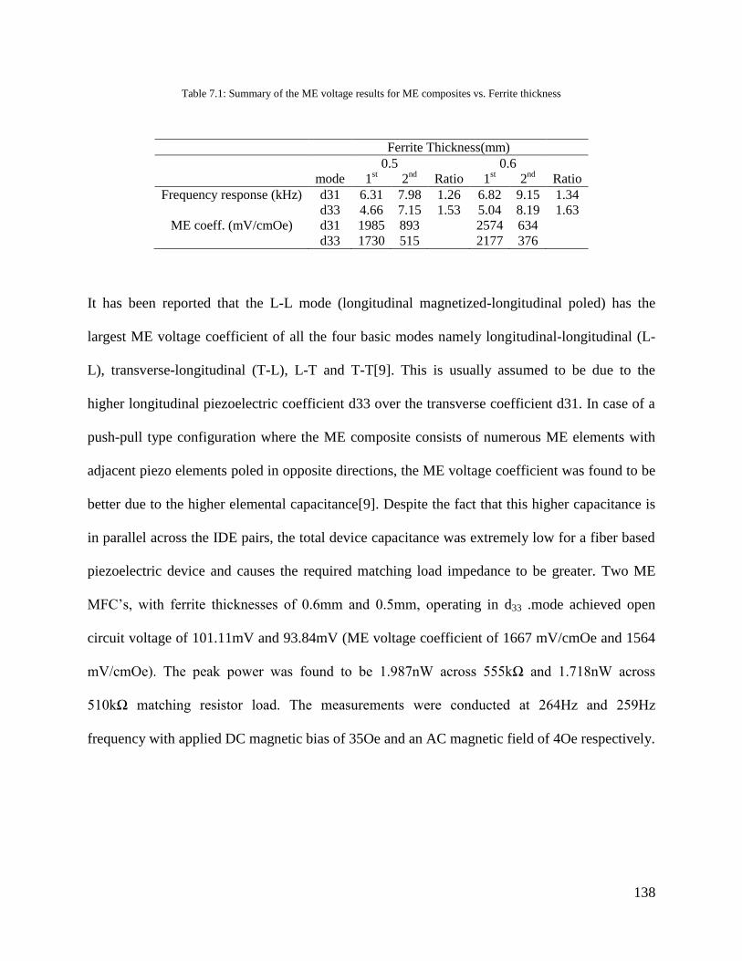
138
Table 7.1: Summary of the ME voltage results for ME composites vs. Ferrite thickness
Ferrite Thickness(mm)
0.5
0.6
mode 1
st 2
nd Ratio 1
st 2
nd Ratio
Frequency response (kHz) d31 6.31 7.98 1.26 6.82 9.15 1.34
d33 4.66 7.15 1.53 5.04 8.19 1.63
ME coeff. (mV/cmOe) d31 1985 893
2574 634
d33 1730 515
2177 376
It has been reported that the L-L mode (longitudinal magnetized-longitudinal poled) has the
largest ME voltage coefficient of all the four basic modes namely longitudinal-longitudinal (L-
L), transverse-longitudinal (T-L), L-T and T-T[9]. This is usually assumed to be due to the
higher longitudinal piezoelectric coefficient d33 over the transverse coefficient d31. In case of a
push-pull type configuration where the ME composite consists of numerous ME elements with
adjacent piezo elements poled in opposite directions, the ME voltage coefficient was found to be
better due to the higher elemental capacitance[9]. Despite the fact that this higher capacitance is
in parallel across the IDE pairs, the total device capacitance was extremely low for a fiber based
piezoelectric device and causes the required matching load impedance to be greater. Two ME
MFC’s, with ferrite thicknesses of 0.6mm and 0.5mm, operating in d33 .mode achieved open
circuit voltage of 101.11mV and 93.84mV (ME voltage coefficient of 1667 mV/cmOe and 1564
mV/cmOe). The peak power was found to be 1.987nW across 555kΩ and 1.718nW across
510kΩ matching resistor load. The measurements were conducted at 264Hz and 259Hz
frequency with applied DC magnetic bias of 35Oe and an AC magnetic field of 4Oe respectively.

139
100000 1000000 1E70.000.010.02
0.030.040.050.06
0.070.08
0.6mm
0.6mm
Voltag
e (
V)
0.0
0.4
0.8
1.2
1.6
2.0
2.4
0.6mm
0.6mm Pow
er
(nW
)
100000 10000000.00
0.01
0.02
0.03
0.04
0.05
0.06
0.07
Resistance (Ohm)
0.4
0.8
1.2
1.6
Figure 7.7 Voltage and power loading curves for 0.5mm (top) and 0.6mm (bottom) ME composite MFC’s.
Due to the 995kΩ resistance of the data acquisition system (which is in parallel to the 555kΩ and
510kΩ matching resistor loads for the 0.6mm and 0.5mm ferrite ME MFC’s), the effective load
seen by the transducer were 356kΩ and 337kΩ for the two ME MFC’s of ferrite thickness of
0.6mm and 0.5mm respectively. This matching impedance amounts to an effective electrical
capacitance of 1.69nF and 1.82nF, respectively. After dicing, MFC fabrication and poling, the
measured capacitance was 0.14nF and 0.118nF at 1kHz respectively. The discrepancy between
the capacitance calculated from the matching impedance and that measured prior to poling
maybe due to a) the frequency difference between the capacitance measurement and that of the
operation and b) resonant operation of the magnetically induced vibration of the piezoelectric. As
shown in the inset of Fig. 7.8(a), the ferrite has a low coercive field of the order of ~20 Oe. The
lowest effective longitudinal field that was achievable was ~35 Oe.

140
a)
-400 -200 0 200 400
-80
-60
-40
-20
0
20
40
60
80
0 100 200 300 400 50040
50
60
70
80
Mag
neti
zati
on
(em
u/g
)
H (Oe)
-40 -30 -20 -10 0 10 20 30 40-40
-30
-20
-10
0
10
20
30
40
Mag
neti
zati
on
(em
u/g
)
H (Oe)
Mag
neti
zati
on
(em
u/g
)
H (Oe)
b)
0.6 0.7 0.8 0.9 1.0 1.1 1.2 1.3 1.4 1.5 1.60
20
40
60
80
100
120
140
160
180
200
-0.2 0.0 0.2 0.4 0.6 0.8 1.0 1.2 1.4 1.6
0
1000
2000
3000
4000
5000
Gaussmeter
Ga
ussm
ete
r (O
e)
Distance (inch)
Gaussmeter
Ga
ussm
ete
r (O
e)
Distance (inch)
Figure 7.8 a) Magnetization-Field (M-H) hysteresis loop for the Electroscience Ferrite 40011 and b) the effective DC Magnetic
bias achievable by using a longitudinally translatable NdFeB magnet
We would like to achieve <100Hz simple cantilever based application and for doing so, the
following options are available: a) add an inertial tip mass, b) decrease stiffness of the support

141
and c) decrease stiffness of the Magnetoelectric composite. The stiffness of the support, the
Copper IDE kapton flexible circuit can be adjusted by using a tape with less copper (less copper
thickness, more space between copper lines, etc), thinner kapton and low elasticity epoxy
between the copper. The stiffness of the ME composite can be adjusted by using lesser thickness
of the magnetostrictive and piezoelectric materials and that of the epoxy in between the ME
fibers.
Conclusion
We developed a low temperature jet vapor solder bonded (<125 oC) magnetoelectric composite
fibers and incorporated them with kapton based copper flexible circuit using a room temperature
curing epoxy. With this bonding approach, we achieved an ME voltage coefficient of 1667
mV/cmOe and 1564 mV/cmOe at 264Hz and 259Hz for 0.6mm and 0.5mm ferrite based MFC’s.
The resulting magnetoelectric macro fiber composites provided low frequency energy harvesting
capability under vibration and magnetic field. Further work is required to optimize the power
generation capability of these magnetoelectric macro fiber composites.
Acknowledgements: The authors gratefully acknowledge the financial support from Air Force
Office of Scientific Research (AFOSR) through Young Investigator Program and Office of
Basic Energy Science, Department of Energy (S.P.). We are also greatly indebted to Justin
Farmer CEHMS Laboratory manager for help with the experimental setup. We also would like to
thank Bret Halpern of Jet Process Corporation, North Haven, CT for the solder deposition and
T.J. Belton and Travis Belton of Moog Components Group Galax Operations, Galax, VA for
flexible circuit fabrication.
142
References
[1] Nan C-W, Liu G, Lin Y. Influence of interfacial bonding on giant magnetoelectric
response of multiferroic laminated composites of Tb[sub 1 - x]Dy[sub x]Fe[sub 2] and PbZr[sub
x]Ti[sub 1 - x]O[sub 3]. Applied physics letters 2003;83:4366.
[2] Liu G, Nan C-W, Cai N, Lin Y. Dependence of giant magnetoelectric effect on interfacial
bonding for multiferroic laminated composites of rare-earth-iron alloys and lead--zirconate--
titanate. Journal of Applied Physics 2004;95:2660.
[3] Gheevarughese V, Laletsin U, Petrov V, Srinivasan G, Fedotov N. Low-frequency and
resonance magnetoelectric effects in lead zirconate titanate and single-crystal nickel zinc ferrite
bilayers. JOURNAL OF MATERIALS RESEARCH-PITTSBURGH THEN WARRENDALE-
2007;22:2130.
[4] Zhao P, Zhao Z, Hunter D, Suchoski R, Gao C, Mathews S, Wuttig M, Takeuchi I.
Fabrication and characterization of all-thin-film magnetoelectric sensors. Applied physics letters
2009;94:243507.
[5] Park C-S, Priya S. Cofired Magnetoelectric Laminate Composites. Journal of the
American Ceramic Society 2011;94:1087.
[6] MacDonald WD, Eagar TW. Transient Liquid Phase Bonding. Annual Review of
Materials Science 1992;22:23.
[7] Roman JW, Eagar TW. Low stress die attach by low temperature transient liquid phase
bonding. PROCEEDINGS-SPIE THE INTERNATIONAL SOCIETY FOR OPTICAL
ENGINEERING: SPIE INTERNATIONAL SOCIETY FOR OPTICAL, 1992. p.52.
[8] Wan JG, Li ZY, Wang Y, Zeng M, Wang GH, Liu J-M. Strong flexural resonant
magnetoelectric effect in Terfenol-D/epoxy-Pb(Zr,Ti)O[sub 3] bilayer. Applied Physics Letters
2005;86:202504.
[9] Zhai J, Xing Z, Dong S, Li J, Viehland D. Magnetoelectric Laminate Composites: An
Overview. Journal of the American Ceramic Society 2008;91:351.
[10] Blevins RD. Formulas for natural frequency and mode shape. New York: Van Nostrand
Reinhold Co., 1979.
[11] Wei-Hua G, Yong-Zhen H, Qiao-Yin L, Li-Juan Y. Whispering-gallery-like modes in
square resonators. Quantum Electronics, IEEE Journal of 2003;39:1106.

143
Chapter 8
Design, Modeling and Experimental Verification of Low
Frequency Resonant Piezo MEMS Structures for Energy
Harvesting
Ronnie Varghese, 1 Shree Narayanan,
2 Donald Leber,
2 and Shashank Priya
1,*
1Center for Energy Harvesting Materials and Systems (CEHMS), Bio-Inspired Materials and Devices Laboratory (BMDL), Virginia Tech,
Blacksburg, VA 24061, USA 2Electrical and Computer Engineering Department, Virginia Tech, Blacksburg, VA 24061, USA
Abstract
In this paper, we report the development of a low frequency (<100Hz) resonant piezo
MEMS structures for energy harvesting. The structures were fabricated on platinized silicon
wafer and bulk piezo material. Pb(Zr,Ti)O3 (PZT) piezoelectric thin film was rf sputtered on
platinized silicon. PZT thin film properties were optimized for energy harvesting by improving
the texture degree with respect to the underlying platinized Si substrate. The silicon MEMS
fabrication process flow consisted of two modules – a) the mechanical module wherein the Si
cantilever structures were created and b) the electrical module for PZT capacitor formation. This
simplified process flow reduces the number of unit operations by ~40%. Using this modular
approach, we studied different cantilever structural designs and based on this learning, conceived
a low frequency structure that resembles a circular labyrinth. We describe various methodologies
for modulation of the natural frequency of a cantilever by varying its cross section dimensions
along three axes. For electrical testing under vibration, a wafer level tester was engineered using
gold plated pogo pins on a custom printed circuit board. As an alternative to cleanroom based Si
144
micromachining processes, circular labyrinth structures were also manufactured from Piezo
sheets, unimorphs and bimorphs using a novel non cleanroom micromachining technique called
microwater jet cutting. This structure has demonstrated <100Hz resonant operation without a tip
mass.
Keywords: Piezoelectric MEMS; energy harvesting; Silicon micromachining; texturing;
frequency tuning
Introduction
Micro scale low frequency energy harvesting has been mainly dominated by inductive or
electromagnetic devices [1, 2]. However, the miniaturization of such devices is limited by the
size of the magnet used as the inertial mass and the size of the coil that can be fabricated in the
MEMS scale. Consequently, for MEMS scale energy harvesting, piezoelectricity is the
transduction of choice and especially due to its compatibility with cleanroom based silicon
micromachining techniques. However, the resonance increases to kHz range on scaling down
low frequency piezoelectric devices to MEMS sizes. Use of large inertial masses on simple
single cantilever beam structures have been reported for low frequency MEMS energy
harvesting[3]. An S-shaped MEMS cantilever system was capable of achieving < 30Hz but
required a substantially large tip mass[4]. Such structures are limited in their power due to the
size of the piezoelectric element. Low frequency structures with larger piezoelectric functional
areas would increase the energy conversion.
We report on a new tip mass free low frequency vibration energy harvesting structure that is
capable of attaining resonant frequencies of less than 100Hz with less torsion than spiral
designs[5] and with a smaller foot print than zigzag [6] or meandering [7] structures. This

145
structure, named Circular Labyrinth or Zigzag, has achieved <100Hz resonant operation both on
the Si MEMS platform and with bulk Piezo material. For Si wafer based fabrication, we report a
new Piezo MEMS Si micromachining process flow which has fewer steps and is simpler to
implement whilst for bulk Piezo, we reveal a new approach of micromachining using a micro
water jet. Non Si wafer based micromachining has been attempted earlier by laser
micromachining – either by laser shaping LTCC tape and then cofiring the shaped tape [8] or
using laser cutting piezo sheets directly[9]. The former is a very elegant way but the laser cut
tape will shrink during sintering and if not carefully sintered can crack across the corners. The
latter is plagued by a heat affected zone that can degrade the piezo properties (by amorphization
and lead loss) in that area of the laser cut cantilever. Micro water jet cutting overcomes such
concerns as it uses a ultrasonic water jet to ablate the piezo material in a required pattern.
Experimental Procedures
Silicon Micromachining
For wafer size deposition of PZT thin films, one can either employ sol-gel or RF sputtering. We
chose RF sputtering due to a) higher deposition rates, b) ease of depositing over topography, c)
ability to control stress and d) ability to integrate into a ‘mechanical-first’ Piezo MEMS
fabrication process. Unlike the standard ‘electrical first’ fabrication process[10], the vibrational
structure is defined and created and then the electrical module with its PZT capacitors is
processed.
Our fabrication process is split into two –mechanical and electrical modules. The mechanical
module consisted of silicon micromachining processing steps. The electrical module comprised
of steps to fabricate the PZT capacitive elements of PZT thin film sandwiched between 2 Pt

146
electrodes. We use 2 shadow masks for a combined bottom Pt and PZT and top Pt depositions
respectively. All wet etch processes are thus avoided. After development of our process flow and
fabrication process, we came across a more complicated mechanical-first process that utilizes
screen printed thick PZT[11]. The electrical module thin film stack consist of 3000A Pt over 1
micron PZT of 2 different stoichiometry’s, Pb(Zr0.60Ti0.40)O3 and Pb(Zr0.52Ti0.48)O3 , over 3000A
Pt with an adhesion layer of 100A Ti. The substrates were 700C O2 annealed PECVD SiO2
coated 0.5mm Si p(100) wafers (has a minor flat at 90 to the major flat permitting easy
assignment of front and back side processing steps). PZT RF sputtering and Pt DC sputtering
was conducted on Aja International ATC Orion system whilst the Ti deposition was conducted
on Kurt Lesker PVD 75E-beam evaporator.
Table 8.1 Unit Operation detail of the 2 modules in a Piezo MEMS process flow
When the modules are combined, our process is unique in that each module is processed on a
specific side of the silicon wafer. Traditionally, dual side processing is required to define the
cantilever. Without the use of an SOI wafer, the cantilever beam thickness is defined first by a
short Deep Reactive Ion Etch (DRIE) from the front side and then a backside DRIE is conducted
to release the structures[12]. We have developed a self-aligned and self-isolated MEMS

147
fabrication process capable of fabricating vibrational structures with an inertial tip mass and with
only 2 photo lithography steps. The key feature of this process is the use of a patterned SiO2 hard
mask to define the beam thickness in the DRIE and then after removal of that SiO2 hard mask,
using a 2nd
patterned photoresist mask to proceed with a 2nd
DRIE to release the cantilever.
Unlike the process used for the unreleased MEMS structure of a Piezo accelerometer[13], our
process is developed to a) in situ remove the SiO2 hard mask before the 2nd
DRIE and b) then
conduct the 2nd
DRIE to the front side for release. The removal of the SiO2 hard mask after the
1st DRIE can be skipped in some cases and the DRIE SiO2:Si etch rate selectivity can be utilized
to define the cantilever beam thickness. That is, after SiO2 hard mask definition and 1st DRIE,
the 2nd
DRIE mask pattern is applied but SiO2 need not be removed. This inorganic hard mask
will etch slower than Si and thus when the Si DRIE reaches the front of the wafer, the sections
that were covered by SiO2 would have lagged behind during etch and would be thicker.

148
Figure 8.1 New Self aligned Mechanical First Electrical Last process
Bulk Piezo Micromachining
PZT has a lower Young’s modulus of elasticity than Si (60 vs 169 GPa) and therefore a
cantilever fabricated out of bulk piezo can be presumed to have lower resonant frequency for the
same shape and beam thickness. Bulk piezo materials like sheets, unimorph and bimorphs etc
can be machined using a) CNC (via size limited by drill bit size, dirty process with cooling fluid)
b) Laser ablation (Slag formation and damage to PZT; low throughput and speed; high cost per
device; via sizes <200 microns possible albeit with slag areas of at least 20 microns) and finally
c) Micro water jet (no damage to PZT; high throughput and speed; cost per device 2/3rd
of laser;
~200um wide via possible; clean process as part is only exposed to water and cutting debris).
Micro Electric discharge machining (EDM) was ruled out as it cannot cut nonconductive
ceramics. Microwaterjet processing prefers a leading edge for start of cut, requires that the
material is loaded onto a fixture (preferably metal) and can provide via widths of ≥ 200microns.
We used PSI-5H4E Piezo sheets and T215-H4-503X series poled bimorphs. Despite the fact that
series poled bimorphs require higher matching loads, they were chosen as numerous reports
claim the high power and voltage generating benefits of series poled over parallel poled
bimorphs [14-16]. The unimorphs were made in house by bonding Ni Alloy 201 from
McMaster-Carr to the aforesaid Piezo sheets. These piezo sheets and composites were then micro
water jet cut into the new low frequency structure reported in this paper.
Wafer level Characterization - Mechanical

149
Figure8.2 Vibration testing setup with perimeter clamping of MEMS wafer
For mechanical testing of MEMS wafers, a Polytec MSA 500 was used with a special clamp that
clamps the wafer along its edges (figure above). As the shaker is moving the whole wafer and all
its MEMS devices simultaneously, we scan each cantilever from tip to base and take the transfer
function between the tip and base to compute the resonance frequency. Typical 3D animation
plots of the actual vibration characteristics are shown below (figure below).
a) b)
Figure 8.3 Animation plots of the Velocity FRF at fundamental resonance of a) a linear zigzag and b) a circular spiral
We utilized a cantilever type (the harvester is clamped in free-clamped mode) Aluminum clamp
mounted onto a TMC Solution TJ-2 electromagnetic shaker which was powered by an HP 6825A
power supply/amplifier operating as a fixed gain amplifier. SigLab 20-42 data acquisition system
with four input channels and two output channels is used for the Voltage frequency response
function (FRF) measurements. This data acquisition system has an internal resistance of 995kΩ
150
and this resistance was in parallel with any load resistance attached externally to the device
under test. The reference acceleration was measured at the clamp using an accelerometer
(Piezotronics Inc. model # U352C67). Voltage generated by the harvester and the power loading
curves were generated by placing a digital IET Labs load resistor in series with the harvesters.
The output signal from the accelerometer was conditioned using a charge amplifier (Piezotronics
Inc.). The velocity at the tip of cantilever beam was measured using a digital vibrometer (Polytec
OFV 353). Polytec 5000 controller was used to generate input signals to the seismic shaker to
create vibration and also to capture the output signals from accelerometer and vibrometer.
Wafer level Characterization - Electrical
At present, MEMS harvesters are tested individually after the wafer has been singulated by
dicing. This requires that the MEMS device be packaged or temporarily glued to a special carrier
wafer to protect the MEMS structures from damage during dicing. Prior to packaging and
singulation, we decided to employ wafer level testing and to do so we introduced a novel concept
of using wafer probe cards fabricated from a PCB with Gold plated pogo pin probes (figure
below). EagleTM
software was used to lay out the pogo pin locations and route the wiring pads to
the perimeter of the PCB. All wiring is thus confined to the outside of the test setup and do not
interfere with the Laser Vibrometry measurement. This approach is especially useful if one has
numerous devices on a wafer (we have 88 different cantilevered devices on our mask layout).

151
Figure 8.4 Electrical test setup: (clockwise from top left) PCB layout design, as manufactured, with pogo pins soldered on and
finally clamped over a device wafer
Results and Discussion
Electrical Module
Thin Film Development
PZT thin film was cold sputtered from internally formed targets of 2 stoichiometry’s,
Pb(Zr0.60Ti0.40)O3 and Pb(Zr0.52Ti0.48)O3(hitherto referred to as PZT 60/40 and PZT 52/48

152
respectively), onto 2 platinized Si substrates – from Inostek (Korea) which has a 1500A Pt
(111)/100A Ti/ 3000A SiO2/Si stack vs. our stack of 3000A Pt/100A Ti/ 10000A SiO2/Si. The
XRD patterns (shown below) from the 2 substrates clearly show random texturing of our Pt vs.
Inostek’s highly (111) Pt.
20 30 40 50 6010
1
102
103
104
105
106
XR
D I
nte
nsity (
arb
.units)
2theta (degrees)
VT's Pt
Inostek Pt
Figure 8.5 XRD pattern of Inostek (red) vs. our Platinized Si
PZT thin films of (100) orientation near the morphotropic phase boundary has the highest
piezoelectric performance [17, 18]. As a) PbO seed layer has been theorized to generate (100)
texturing of PZT [19] and b) PbO has a very high vapor pressure, we annealed our platinized Si
substrates in closed (but not air tight) environment along with PbO powder. We postulated that
the PbO will sublime on heating and then on cooling would condense on the Pt. However from
the figures below, PbO sublimation at 600°C for 5hrs seemed to randomize the PZT structure
irrespective of whether it was sputtered or sol-gel PZT.

153
a)
20 25 30 35 40 45 50 55 60 650
2000
4000
6000
8000
100000
2000
4000
6000
8000
10000
PZT 52/48
2theta (degrees)
VT's Pt
(110)
(100) (211)(111)
Pt
PbO+PZT 52/48 VT's Pt
Pt
b)
20 25 30 35 40 45 50 55 60 65
0
2000
4000
6000
8000
100000
2000
4000
6000
8000
10000
PbO+PZT solgel
2theta (degrees)
Inostek Pt
Pt-Ti
PZT solgel
Inostek Pt
(200)
(100)
Figure 8.6 a) sputtered PZT 52/48 and b) sol-gel PZT 60/40 on PbO sublimed over Inostek platinized Si
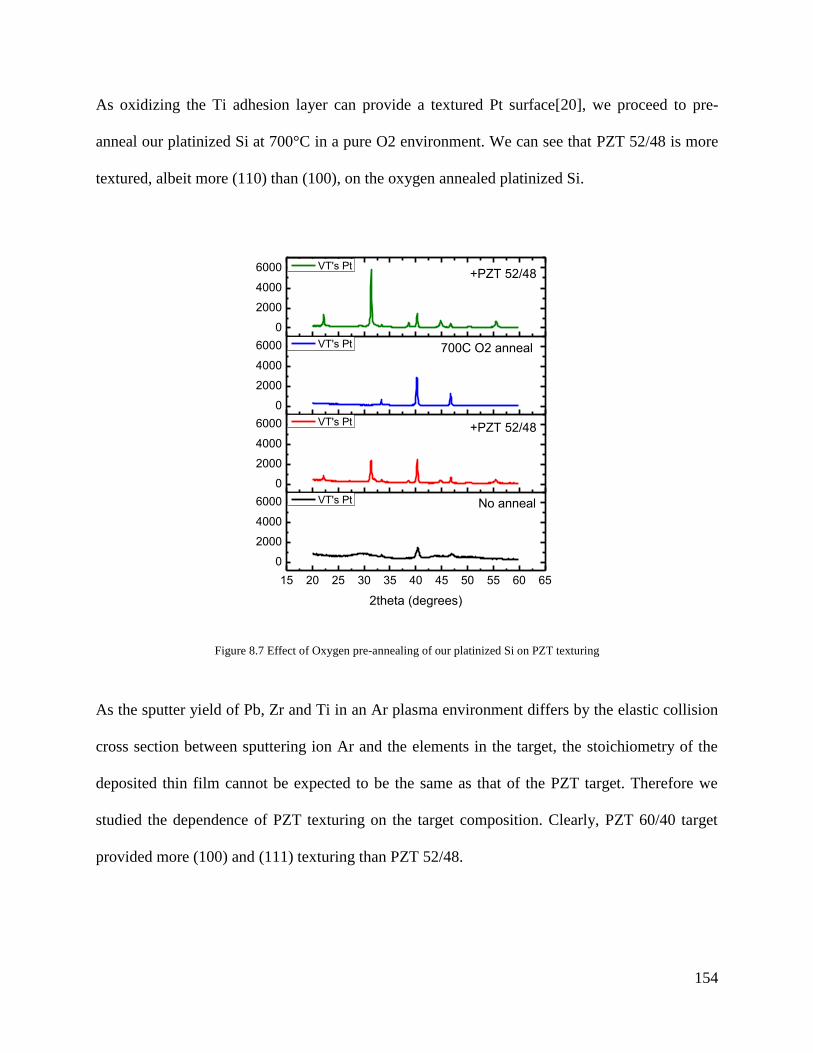
154
As oxidizing the Ti adhesion layer can provide a textured Pt surface[20], we proceed to pre-
anneal our platinized Si at 700°C in a pure O2 environment. We can see that PZT 52/48 is more
textured, albeit more (110) than (100), on the oxygen annealed platinized Si.
15 20 25 30 35 40 45 50 55 60 65
0
2000
4000
6000
0
2000
4000
6000
0
2000
4000
6000
0
2000
4000
6000
No anneal
2theta (degrees)
VT's Pt
+PZT 52/48 VT's Pt
700C O2 anneal VT's Pt
+PZT 52/48 VT's Pt
Figure 8.7 Effect of Oxygen pre-annealing of our platinized Si on PZT texturing
As the sputter yield of Pb, Zr and Ti in an Ar plasma environment differs by the elastic collision
cross section between sputtering ion Ar and the elements in the target, the stoichiometry of the
deposited thin film cannot be expected to be the same as that of the PZT target. Therefore we
studied the dependence of PZT texturing on the target composition. Clearly, PZT 60/40 target
provided more (100) and (111) texturing than PZT 52/48.

155
15 20 25 30 35 40 45 50 55 60 65
102
103
104
105
10610
2
103
104
10510
2
103
104
105
106
PZT 60/40
2Theta (degrees)
As deposited
PZT 60/40 700C 15min
(111)(200)
(211)
PZT 52/48 700C 15min
(100) (110)
Pt
Figure 8.8 PZT texturing dependence on stoichiometry of the sputtering target
Since a) the piezoelectric coefficient in d33 mode is almost twice that in d31 mode and b)
traditionally used ZrO2 charge barrier layer deposition was not available, we investigated the use
of Atomic layer deposited (ALD) Al2O3 and HfO2 on PZT texturing. From the figure below,
both amorphous ALD films seem to randomize the PZT.

156
15 20 25 30 35 40 45 50 55 60 6510
1
102
103
101
102
103
102
103
104
105
2theta (degrees)
700C 15minAl
2O
3
700C 15min
(100)
(210)
Si
HfO2
Inostek Pt 700C 15min Pt
(110)
(111)
(200)
(211)
Figure 8.9 Effect of ALD thin films of Al2O3 and HfO2 on PZT texturing
Mechanical Module
X-Y Cross section variation
The pictures below depict clockwise from top left – 300um width, 200um cantilever, Taper
wider end clamped (300um to 200um), Parabolic (300um to 200um to 300um) , Taper narrower
end clamped (200um to 300um) cantilevers and finally a Bezier. All these cantilevers have the
same length and thickness, have beziers at their clamped end and vary only along their widths.
The resonance frequency is in the order (Table 8.2 8.2), Taper wider end clamped >
300um=200um > Parabolic > Taper narrower end clamped and for each type. Tapering wider
end towards clamp is similar to the triangular and trapezoidal shaped harvesters reported already

157
reported in literature [21-24]. For similar footprint as an equivalent rectangular device, such
devices have been shown to have much higher power output as these cantilevers have wider
clamped ends (where the stress is maximum).
Adding a Bezier at the clamped end increased the frequency slightly. Adding such trapezoidal or
even a circular Bezier, spreads the stress distribution near the clamp, improves the tolerance to
acceleration, and alleviates residual stress induced cantilever breakage but sometimes at the cost
of power reduction[25]. But if the Bezier is less than 20% of the length of the beam, there is
considerable improvement in power harvested due to a) larger stress distribution and b) higher
accelerations possible.
Figure 8.10 Cantilevers with varying widths and a Bezier at clamped end
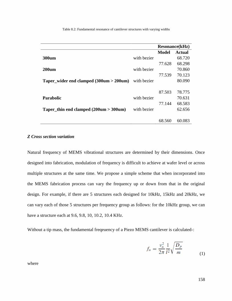
158
Table 8.2: Fundamental resonance of cantilever structures with varying widths
Resonance(kHz)
Model Actual
300um with bezier 68.720
77.628 68.298
200um with bezier 70.860
77.539 70.123
Taper_wider end clamped (300um > 200um) with bezier 80.090
87.503 78.775
Parabolic with bezier 70.631
77.144 68.583
Taper_thin end clamped (200um > 300um) with bezier 62.656
68.560 60.083
Z Cross section variation
Natural frequency of MEMS vibrational structures are determined by their dimensions. Once
designed into fabrication, modulation of frequency is difficult to achieve at wafer level or across
multiple structures at the same time. We propose a simple scheme that when incorporated into
the MEMS fabrication process can vary the frequency up or down from that in the original
design. For example, if there are 5 structures each designed for 10kHz, 15kHz and 20kHz, we
can vary each of those 5 structures per frequency group as follows: for the 10kHz group, we can
have a structure each at 9.6, 9.8, 10, 10.2, 10.4 KHz.
Without a tip mass, the fundamental freqeuency of a Piezo MEMS cantilever is calculated-:
(1)
where
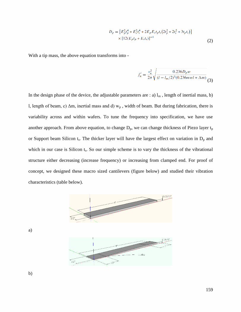
159
(2)
With a tip mass, the above equation transforms into -
(3)
In the design phase of the device, the adjustable parameters are : a) lm , length of inertial mass, b)
l, length of beam, c) Δm, inertial mass and d) wp , width of beam. But during fabrication, there is
variability across and within wafers. To tune the frequency into specification, we have use
another approach. From above equation, to change Dp, we can change thickness of Piezo layer tp
or Support beam Silicon ts. The thicker layer will have the largest effect on variation in Dp and
which in our case is Silicon ts. So our simple scheme is to vary the thickness of the vibrational
structure either decreasing (increase frequency) or increasing from clamped end. For proof of
concept, we designed these macro sized cantilevers (figure below) and studied their vibration
characteristics (table below).
a)
b)

160
c)
Figure 8.11 a) Flat b) Angled and c) 50” Radius of curvature beam
Table 8.3 Fundamental resonance of cantilevers of varying thickness across their length
( Hz) Flat Radius - Clamped
at thick end
Radius -
Clamped at thin
end
Angled -
Clamped at thick
end
Angled -
Clamped at thin
end
No
mass
173.7
9
211.35 47.57 226.07 50.77
With tip
mass
114.6
5
91.65 28.45 105.59 32.22
From the above table, the effect of which end is clamped and that of adding an inertial mass is
pronounced. On adding a tip mass, the resonant frequency of the variable cross section beam
decreases below that of the flat simple beam. In addition, for no tip mass, if the variable cross
section beams are clamped on their thicker end, the frequency increases from that of the thinner
end clamping and that of the flat beam. With a tip mass, a gradient in width decreases the
frequency from that of the flat beam but the frequency of thicker end clamping is greater than
thinner end clamping. This fact can be used for tuning of resonance frequency of MEMS beams
inside the fab without changing the device layout dimensions (figure below).

161
Figure 8.12: Proposed methodology to tune the frequency of partially or fully manufactured MEMS structures with tip mass
Low Frequency Structures
a)
b)
Figure 8.13 Silicon MEMS cantilever structures a) As fabricated b) CAD-generated
The 1st resonance mode of various curvilinear and rectilinear wound structures (figure above) for
full wafer thickness of 0.5mm is shown below. Clearly, the resonance of the 3 turn Circular
Simple Cantilever Linear Zigzag Square Spiral Circular Cantilever Circular Spiral Circular Zigzag

162
zigzag or labyrinth structure is similar to that of a similarly sized 3 turn spiral structure and
dimensionally larger 5 beam zigzag.
Table 8.4 Fundamental resonance of non-linear cantilever structures
Resonance (kHz)
Model Actual
4 turn Circular Spiral 6.065 6.710
3 turn Circular Spiral 12.637 13.413
3 turn Circular Zigzag 12.938 13.406
2 turn Circular Zigzag 34.070 38.688
3 arc Circular cantilever long arc 20.644 20.787
middle arc 44.747 45.063
short arc 76.514 77.370
2.5 turn Square Spiral 16.825 15.450
2 turn Square Spiral 40.345 36.190
3 beam Linear Zigzag 28.883 33.130
5 beam Linear Zigzag 13.464 13.550
We micro water jet cut 18mm diameter 4 turn and 5 turn Circular zigzag patterns in Piezo sheets,
unimorphs and Bimorphs as shown below. The vias were a maximum of 235 microns wide.
Figure 8.14 Micro water jet cut Piezo sheets – 4 turn Circular Zigzag on left and 5 turn on right

163
The vibration and harvesting characteristics at 0.1g acceleration are summarized below.
Undoubtedly, the bimorph with its dual layer piezo has the best energy harvesting performance
and all the piezo structures achieved < 100Hz performance without a tip mass. From the power
loading (Voltage and Power vs. Matching resistance load) curves, we can clearly see that the
optimal load varies with type of device and structure. Despite having almost similar surface areas
(CZ4 = 246.01mm2 vs. CZ5 = 243.08mm
2), CZ5 structure has a higher matching load than the
CZ4 structure across all piezo stacks and expectedly so due to the lower resonance frequency of
the 5 turn structure. The voltage performance shows that the strain created in these structures are
independent of the number of turns.
Table 8.5 Vibration (0.1g) and Electrical Harvesting performance of the Micro water ject cut devices
Frequency
(Hz)+/- 3dB
Sheet Unimorph Bimorph
CZ4 52.71 +/- 1 64.0+/-2.5 89.3 +/-5.7
CZ5 43.25 +/- 0.5 37.75+/-4.25 67.74 +/-4.97
Voltage (Voc ,V) Sheet Unimorph Bimorph
CZ4 0.138 0.567 1.842
CZ5 0.196 0.639 1.294
Power(μW) Sheet Unimorph Bimorph
CZ4 1.02 5.466 52.89
CZ5 1.288 7.232 18.88

164
a)
0 20000 40000 60000 80000 1000000.08
0.10
0.12
0.14
0.16
0.18
CZ5 H4 0.191mm
CZ5 H4 0.191mm
Vo
lta
ge
(V
)0.20.30.40.50.60.70.80.91.01.1
Po
we
r (
W)
0 50000 100000 150000 200000
0.05
0.10
0.15
0.20
0.25
CZ4 H4 0.191mm
CZ4 H4 0.191mm
Resistance (Ohm)
0.2
0.4
0.6
0.8
1.0
1.2
1.4
b)
0.1
0.2
0.3
0.4
0.5
0.6
CZ5 H4 0.191mm+3mil Ni
CZ5 H4 0.191mm+3mil Ni
Vo
lta
ge
(V
)
1
2
3
4
5
6
Po
we
r (
W)
0 20000 40000 60000 80000 100000
0.2
0.3
0.4
0.5
0.6
CZ4 H4 0.127mm+2mil Ni
CZ4 H4 0.127mm+2mil Ni
Resistance (Ohm)
3.54.04.55.05.56.06.57.07.5
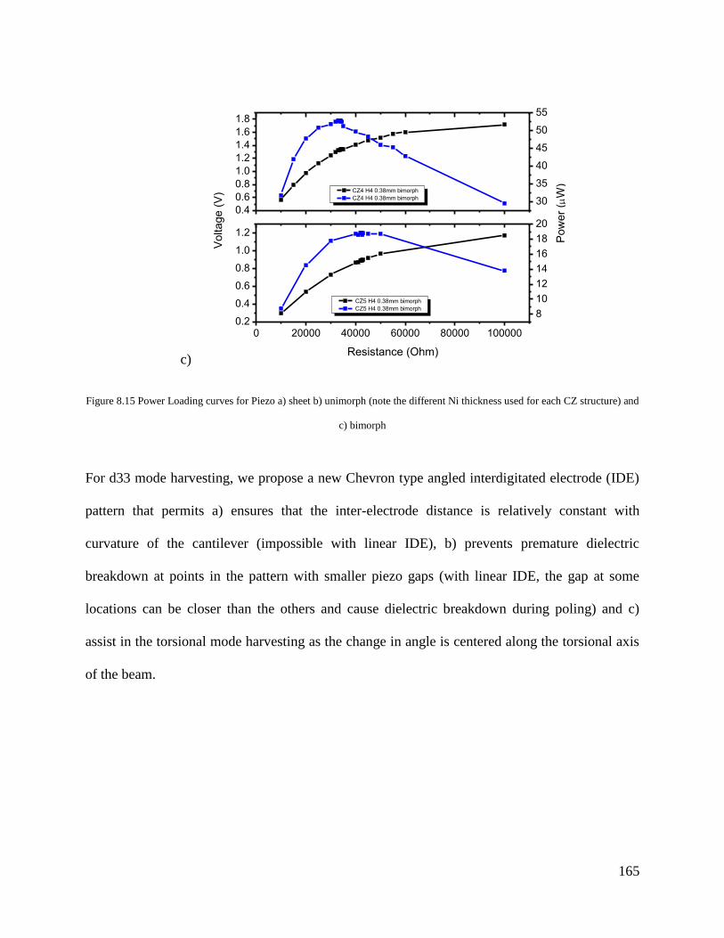
165
c)
0.4
0.6
0.8
1.0
1.2
1.4
1.6
1.8
CZ4 H4 0.38mm bimorph
CZ4 H4 0.38mm bimorph
Vo
lta
ge
(V
)
30
35
40
45
50
55
0 20000 40000 60000 80000 1000000.2
0.4
0.6
0.8
1.0
1.2
CZ5 H4 0.38mm bimorph
CZ5 H4 0.38mm bimorph
Resistance (Ohm)
8
10
12
14
16
18
20
Po
we
r (
W)
Figure 8.15 Power Loading curves for Piezo a) sheet b) unimorph (note the different Ni thickness used for each CZ structure) and
c) bimorph
For d33 mode harvesting, we propose a new Chevron type angled interdigitated electrode (IDE)
pattern that permits a) ensures that the inter-electrode distance is relatively constant with
curvature of the cantilever (impossible with linear IDE), b) prevents premature dielectric
breakdown at points in the pattern with smaller piezo gaps (with linear IDE, the gap at some
locations can be closer than the others and cause dielectric breakdown during poling) and c)
assist in the torsional mode harvesting as the change in angle is centered along the torsional axis
of the beam.

166
Figure 8.16 Chevron interdigitated electrode pattern for d33 mode energy harvesting
Conclusion
We have demonstrated the first tip mass free <100Hz resonant energy harvesting device by using
a circular labyrinth vibration structure. We have utilized both Si and Piezo micromachining to
fabricate these structures. We achieved an average of 1.15, 6.35 and 35.89 µW for Piezo sheet,
unimorph and bimorph respectively. The exceptional energy harvesting performance of these
structures was realized at very a low acceleration of 0.1g. 5 turn structure provides lower
frequency and requires higher matching load. We describe various techniques for tuning the
resonant frequency of MEMS cantilevers using variable cross sections in the x-y and z
dimensions. We detail a novel approach to the Si wafer based Piezo MEMS fabrication process.
A wafer level testing methodology has been developed for vibration MEMS testing. Finally, we

167
explain different techniques utilized to obtain the harvester constituent RF sputtered PZT thin
films.
Acknowledgements: The authors gratefully acknowledge the financial support from Air Force
Office of Scientific Research (AFOSR).We are also greatly indebted our CEHMS
colleagues, Anthony Marin, Amin Karami, and Reema Gupta for assistance with metrology
assistance, Daniel Apo for ANSYS modeling and John Bird for PCB design and fabrication
assistance.
References
[1] Jong Cheol P, Dong Hyun B, Jae Yeong P. Micro-Fabricated Electromagnetic Power
Generator<newline/> to Scavenge Low Ambient Vibration. Magnetics, IEEE Transactions on
2010;46:1937.
[2] Wang P, Tanaka K, Sugiyama S, Dai X, Zhao X, Liu J. A micro electromagnetic low
level vibration energy harvester based on MEMS technology. Microsyst Technol 2009;15:941.
[3] Shen D, Park J-H, Noh JH, Choe S-Y, Kim S-H, Wikle Iii HC, Kim D-J. Micromachined
PZT cantilever based on SOI structure for low frequency vibration energy harvesting. Sensors
and Actuators A: Physical 2009;154:103.
[4] Liu H, Lee C, Kobayashi T, Tay C, Quan C. A new S-shaped MEMS PZT cantilever for
energy harvesting from low frequency vibrations below 30 Hz. Microsystem Technologies
2012;18:497.
[5] Amin Karami M, Yardimoglu B, Inman DJ. Coupled out of plane vibrations of spiral
beams for micro-scale applications. Journal of Sound and Vibration 2010;329:5584.
[6] Amin Karami M, Inman DJ. Parametric Study of Zigzag Microstructure for Vibrational
Energy Harvesting. Microelectromechanical Systems, Journal of 2012;21:145.
[7] Berdy DF, Srisungsitthisunti P, Byunghoo J, Xianfan X, Rhoads JF, Peroulis D. Low-
frequency meandering piezoelectric vibration energy harvester. Ultrasonics, Ferroelectrics and
Frequency Control, IEEE Transactions on 2012;59:846.
[8] Sobocinski M, Leinonen M, Juuti J, Jantunen H. Monomorph piezoelectric wideband
energy harvester integrated into LTCC. Journal of the European Ceramic Society 2011;31:789.
[9] Kim H, Bedekar V, Islam RA, Woo-ho L, Leo D, Priya S. Laser-machined piezoelectric
cantilevers for mechanical energy harvesting. Ultrasonics, Ferroelectrics and Frequency Control,
IEEE Transactions on 2008;55:1900.
[10] Lee B, Lin S, Wu W, Wang X, Chang P, Lee C. Piezoelectric MEMS generators
fabricated with an aerosol deposition PZT thin film. Journal of Micromechanics and
Microengineering 2009;19:065014.

168
[11] Xu R, Lei A, Dahl-Petersen C, Hansen K, Guizzetti M, Birkelund K, Thomsen EV,
Hansen O. Screen printed PZT/PZT thick film bimorph MEMS cantilever device for vibration
energy harvesting. Sensors and Actuators A: Physical 2012;188:383.
[12] Shen D, Park J-H, Ajitsaria J, Choe S-Y, Wikle III HC, Kim D-J. The design, fabrication
and evaluation of a MEMS PZT cantilever with an integrated Si proof mass for vibration energy
harvesting. Journal of Micromechanics and Microengineering 2008;18:055017.
[13] Yu HG, Wolf R, Deng K, Zou L, Tadigadapa S, Troilier-McKinstry S. Fabrication and
performance of d33-mode lead-zirconate-titanate (PZT) MEMS accelerometers. vol. 4559, 2001.
p.130.
[14] Ng TH, Liao WH. Sensitivity Analysis and Energy Harvesting for a Self-Powered
Piezoelectric Sensor. Journal of Intelligent Material Systems and Structures 2005;16:785.
[15] Aktakka EE, Peterson RL, Najafi K. Multi-layer PZT stacking process for piezoelectric
bimorph energy harvesters. Diamond 2011;10:8000.
[16] Lee BS, Lin SC, Wu WJ. Fabrication and Evaluation of a MEMS Piezoelectric Bimorph
Generator for Vibration Energy Harvesting. Journal of Mechanics 2010;26:493.
[17] Muralt P. Recent Progress in Materials Issues for Piezoelectric MEMS. Journal of the
American Ceramic Society 2008;91:1385.
[18] Du X-h, Zheng J, Belegundu U, Uchino K. Crystal orientation dependence of
piezoelectric properties of lead zirconate titanate near the morphotropic phase boundary. Applied
Physics Letters 1998;72:2421.
[19] Chen S-Y, Chen IW. Temperature–Time Texture Transition of Pb(Zr1−xTix)O3 Thin
Films: I, Role of Pb-rich Intermediate Phases. Journal of the American Ceramic Society
1994;77:2332.
[20] Sanchez L, Potrepka D, Fox G, Takeuchi I, Polcawich R. Improving PZT Thin Film
Texture Through Pt Metallization and Seed Layers. MRS Online Proc. Library 2011;1299.
[21] Baker J, Roundy S, Wright P. Alternative geometries for increasing power density in
vibration energy scavenging for wireless sensor networks. Proc. 3rd Int. Energy Conversion
Engineering Conf.(San Francisco, CA, Aug.), 2005. p.959.
[22] Park J-H, Kang J, Ahn H, Kim S-B, Liu D, Kim D-J. Analysis of Stress Distribution in
Piezoelectric MEMS Energy Harvester Using Shaped Cantilever Structure. Ferroelectrics
2010;409:55.
[23] Frey A, Seidel J, Schreiter M, Kuehne I. Piezoelectric MEMS energy harvesting module
based on non-resonant excitation. Solid-State Sensors, Actuators and Microsystems Conference
(TRANSDUCERS), 2011 16th International, 2011. p.683.
[24] Goldschmidtboeing F, Woias P. Characterization of different beam shapes for
piezoelectric energy harvesting. Journal of micromechanics and microengineering
2008;18:104013.
[25] Defosseux M, Allain M, Basrour S. Comparison of different beam shapes for
piezoelectric vibration energy harvesting. Proc. of PowerMEMS 2010 The 10th International
Workshop on Micro and Nanotechnology for Power Generation and Energy Conversion
Applications, 2010.
169
Chapter 9
Dispersion Passivated Copper Ink Printing: a New
Approach for Oxidation Resistance
Ronnie Varghese,1 Yu Zhao,
1 Elliot McCallister,
1 Alex O. Aning
2 and Shashank Priya
1,*
1Center for Energy Harvesting Materials and Systems (CEHMS), Bio-Inspired Materials and Devices Laboratory (BMDL), Virginia Tech,
Blacksburg, VA 24061
2Materials Science and Engineering Department, Virginia Tech, Blacksburg, VA 24061, USA
Abstract
In this paper, we report a new approach to passivation of copper thin films and
interconnects using metallic oxide dispersion. Unlike metallic doping or alloying, this method is
uniquely suited to wet chemical deposition techniques like electroplating, ink jet printing, spin
coating, sol-gel, etc. Sol-gel chemistry is used to introduce dopant metallic alkoxides into the
copper ink or solution. Subsequent thermal treatment of the copper thin film or interconnect line
brings the dopants to the surface where they form a passivating oxide layer. Magnesium and
Aluminum were chosen as the dopant metals and their alkoxides were employed. The stabilized
sols of Magnesium and Aluminum alkoxides were mixed with the copper ink in < 5 mol%
concentrations and the copper solutions spun coated on oxidized silicon substrates. The
resistivity was measured by Van der Pauw 4 point probe to be 10.1 µΩ-cm which is 10x that of
pure copper (1.67 µΩ-cm). Corrosion testing show that doped copper films has a high resistivity
outer protective layer of the dopant metallic oxide.

170
Introduction
Copper based interconnects form the basic routing in most CMOS based CPU chips.
Miniaturized Copper based coils are being in RF devices and inductive energy harvesters. Due to
easier availability, processing and reliability of Copper, it has been the conductor of choice in
printed circuitry. Copper is easily oxidized during ambient air heat treatment and has low
oxidation resistance. Copper ink based 3D printing has been developed for industrial use but
suffers from the need to cure the ink in an oxygen free environment (usually forming or inert
gas). Pulsed light or photonic sintering has been employed to cure Copper ink with minimal
oxidation in air[1]. The micro to milli seconds of high intensity pulsed UV light exposure cause
extremely localized heating without damaging any organic substrate below the printed copper
ink. However, such light sources and control equipment are expensive and require special ozone
sensors and abatement. Below 10nm, the melting point of copper decreases considerably and so
nanoparticle based ink has been developed to lower curing or sintering temperature This
methodology was used to lower the sintering temperature to 200°C but with the consequence of
high resistivity of 40 µΩ-cm [2]. Organically stabilized copper nanoparticle ink has been shown
to enable low temperature curing albeit in inert or forming gas ambience[3]. However, this post
cured Copper is still susceptible to oxidation whilst copper interconnects alloyed with Al has
been shown to have high oxidation resistance[4]. Therefore, a post cured corrosion resistant
copper ink would be extremely advantageous.
For ambient atmosphere sintering, alloying Cu metallization interconnects with a few atomic %
of Al and Mg has been shown to be very effective[5]. The oxidation resistance of these alloyed
Cu was orders of magnitude greater than that of undoped Cu. On heat treatment in ambient air,
the Al and Mg, though deposited as Cu-Al and Cu-Mg alloys, were found to diffuse out to the Cu
171
surface and oxidize to form a passivating layer. The key properties of the alloying element is that
it should have a) high diffusivity in copper, b) high free energy formation of oxide, c) below Cu
in Ellingham diagram, d) minimal increase in the resistivity of copper, e) low solubility in copper
and f) alloy should be mechanically stronger[6].
In order to replicate the same phenomenon in Copper nanoparticle ink, Al and Mg nanoparticles
have to be used. Al and Mg nanoparticles are considered biological[7] and explosion[8] hazards
for ambient use. One approach is to use core-shell nanoparticles of Cu-Al and Cu-Mg and such
technology has been tried to create Cu-Ag core-shell nanoparticles[9]. However the fabrication
process is complicated and often unstable. At the time of writing, we were unable to find a Cu-Al
or Cu-Mg core-shell process in literature. So we decided to explore the possibility of using
organometallic compounds of Al and Mg. Such compounds were found to be rare, difficult to
synthesize and highly unstable. However, alkoxides of Al and Mg are ready available and stable
especially in the liquid form necessary to mix with the Cu ink. Salts of Al and Mg were ruled out
due to their hygroscopic nature. Al and Mg alkoxides can also be diluted or dissolved to the
required doping concentration in organic solvents. However, Al and Mg alkoxides have oxygen
directly bonded to the metal ion and so we are not introducing the dopant metal into copper as an
alloying element but as oxide dispersed in it. Al2O3 and MgO dispersion strengthened copper has
been used for decades in copper wires and high temperature applications [10, 11].
Experimental Procedures
We procured Copper nanoparticle ink Cu-iJ70 from Applied Nanotech, Inc. and as per the
MSDS, it contains Copper in ethyl acetate, glycol ether and other proprietary compounds. The
Cu-iJ70 ink has particle sizes ranging from 20-100nm with an average of 70nm. The solid

172
content weight is 40%. The vendor recommended conditions for pyrolysis is 100C for 30-60min
and a final anneal in forming gas N2/H2 (H2 <4%) at 350°C for 45min (with 30min ramp). As per
the vendor specifications, the final resistivity of the cured ink is 5-7 µΩ-cm.
To this base ink, we added the Al and Mg alkoxides dissolved in organic solvents with or
without chelating agents. The alkoxides employed were Aluminum-tri-sec-butoxide (97%,
Sigma Aldrich), Magnesium ethoxide (98%, Sigma Aldrich) and Magnesium methoxide in
methanol (6-10 wt. %, Sigma Aldrich). The solvents utilized were Ethyl acetate (99.8%, Sigma-
Aldrich), 1-butanol (99%, Sigma-Aldrich) and 1-Octanol (99%, Alfa-Aesar). The chelating
agents were Triethanolamine (TEA, 99%, Sigma-Aldrich), Diethanolamine (DEA, 99%, Sigma-
Aldrich) and Acetic Acid (99%, Sigma-Aldrich). Acetic Acid has been used to stabilize Mg
methoxide in methanol solutions[12]. DEA and TEA were used to stabilize Al tri-sec-butoxide in
butanol solutions[13]. The doping concentration was typically 1-5mol% in copper ink. A
summary of the dopant solutions are tabulated below.
Table 9.1 Ingredients of the Dopant solutions
Designation Metal Alkoxide Solvent Chelating Agent
A Al tri-sec-butoxide 1-butanol TEA
B Al tri-sec-butoxide 1-butanol DEA
C Al tri-sec-butoxide Ethyl Acetate DEA
D Al tri-sec-butoxide Ethyl Acetate TEA
E Magnesium methoxide Methanol Acetic Acid
F Magnesium methoxide Methanol DEA
G Magnesium methoxide 2-Methoxyethanol
I Magnesium ethoxide 2-Methoxyethanol
O Magnesium methoxide Methanol, Octanol DEA
K Al tri-sec-butoxide Octanol DEA
L Al tri-sec-butoxide Octanol TEA

173
The doped ink was then spun coated for 5sec at 500rpm, 5sec at 1500rpm and finally for 20sec at
3000rpm on 1000A SiO2 on 0.5mm Si substrates. The as coated samples were then pyrolized at
120C on a hot place for 40sec and then annealed in ambient air in a furnace at 350C for 45min
(ramp rate of 30min). The resistivity of the uniformly coated films was measured using Van der
Pauw 4 point probe method on a Keithley SCS 4200. The films were then annealed 2 more times
at the same conditions and X-ray diffraction studies were performed after each anneal. To
determine the extent of Copper oxidation with depth, X-ray photoelectron spectroscopy depth
profile of the thin films were also attempted.
Results and Discussion
Firstly, we were unable to pyrolyse our doped Copper samples for the vendor recommended 30-
60min in air as the dopant solution caused agglomeration of the copper film. Only dopant
solutions C, E, F, K, L and O gave stable mixtures with the ANI copper ink and therefore the
most uniform spun coated films. After pyrolysis and furnace sintering, an SEM image of doped
Copper ink E sample shows similar density of structure as undoped copper ink sample.
a)
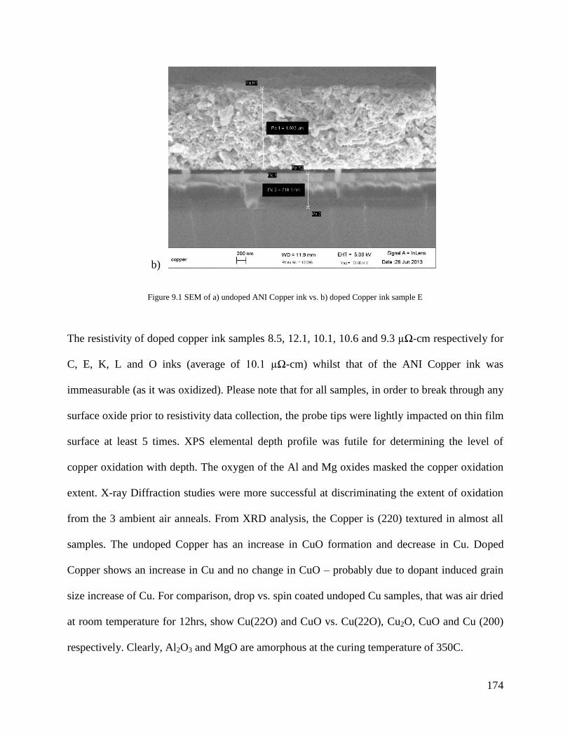
174
b)
Figure 9.1 SEM of a) undoped ANI Copper ink vs. b) doped Copper ink sample E
The resistivity of doped copper ink samples 8.5, 12.1, 10.1, 10.6 and 9.3 µΩ-cm respectively for
C, E, K, L and O inks (average of 10.1 µΩ-cm) whilst that of the ANI Copper ink was
immeasurable (as it was oxidized). Please note that for all samples, in order to break through any
surface oxide prior to resistivity data collection, the probe tips were lightly impacted on thin film
surface at least 5 times. XPS elemental depth profile was futile for determining the level of
copper oxidation with depth. The oxygen of the Al and Mg oxides masked the copper oxidation
extent. X-ray Diffraction studies were more successful at discriminating the extent of oxidation
from the 3 ambient air anneals. From XRD analysis, the Copper is (220) textured in almost all
samples. The undoped Copper has an increase in CuO formation and decrease in Cu. Doped
Copper shows an increase in Cu and no change in CuO – probably due to dopant induced grain
size increase of Cu. For comparison, drop vs. spin coated undoped Cu samples, that was air dried
at room temperature for 12hrs, show Cu(22O) and CuO vs. Cu(22O), Cu2O, CuO and Cu (200)
respectively. Clearly, Al2O3 and MgO are amorphous at the curing temperature of 350C.
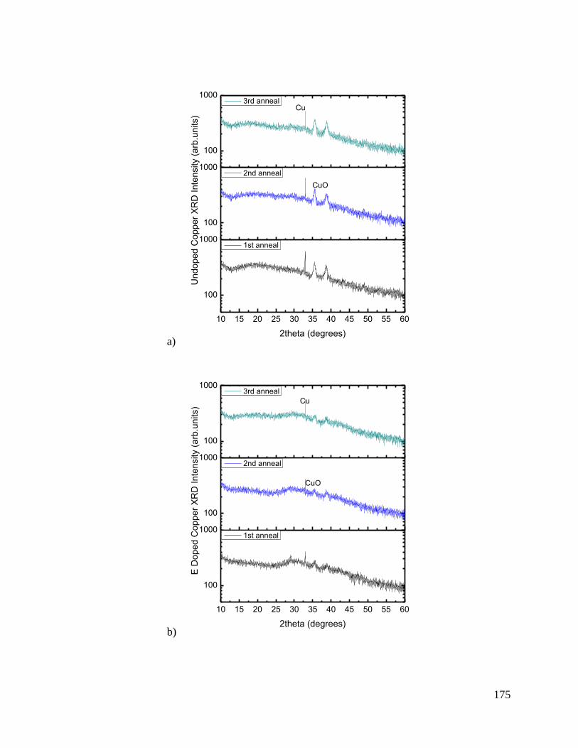
175
a)
10 15 20 25 30 35 40 45 50 55 60
100
1000
100
1000
100
1000
2theta (degrees)
1st anneal
Un
do
pe
d C
op
pe
r X
RD
In
ten
sity (
arb
.un
its)
2nd anneal
CuO
3rd annealCu
b)
10 15 20 25 30 35 40 45 50 55 60
100
1000
100
1000
100
1000
2theta (degrees)
1st anneal
E D
op
ed
Co
pp
er
XR
D I
nte
nsity (
arb
.un
its)
2nd anneal
CuO
Cu
3rd anneal
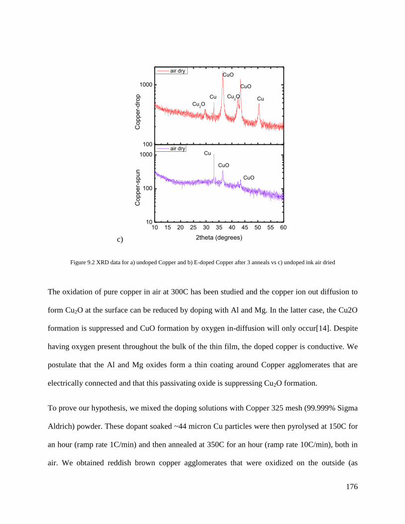
176
c)
10 15 20 25 30 35 40 45 50 55 6010
100
1000
100
1000
Co
pp
er-
sp
un
2theta (degrees)
air dry
CuO
CuO
Cu
CuO
CuO
Cu2O
CuCu2OCu
Co
pp
er-
dro
p
air dry
Figure 9.2 XRD data for a) undoped Copper and b) E-doped Copper after 3 anneals vs c) undoped ink air dried
The oxidation of pure copper in air at 300C has been studied and the copper ion out diffusion to
form Cu2O at the surface can be reduced by doping with Al and Mg. In the latter case, the Cu2O
formation is suppressed and CuO formation by oxygen in-diffusion will only occur[14]. Despite
having oxygen present throughout the bulk of the thin film, the doped copper is conductive. We
postulate that the Al and Mg oxides form a thin coating around Copper agglomerates that are
electrically connected and that this passivating oxide is suppressing Cu2O formation.
To prove our hypothesis, we mixed the doping solutions with Copper 325 mesh (99.999% Sigma
Aldrich) powder. These dopant soaked ~44 micron Cu particles were then pyrolysed at 150C for
an hour (ramp rate 1C/min) and then annealed at 350C for an hour (ramp rate 10C/min), both in
air. We obtained reddish brown copper agglomerates that were oxidized on the outside (as

177
determined by a continuity check with a multimeter) but were as conductive as copper powder in
the inside.
Conclusion
We report the successful use of Aluminum and Magnesium alkoxide in Copper nanoparticle ink
to alleviate the oxidation of Copper during ambient air sintering at 350C. On curing, these
alkoxides in <5 mol% concentrations created copper agglomerates in a matrix of Aluminum or
Magnesium oxides. These copper agglomerates were fused enough to create electrical
connectivity. To prove the matrix theory, we created slurries of pure micron sized copper
particles in the alkoxide solutions and then sintered them in crucibles. The surfaces of these
copper agglomerates were oxidized and not conductive but the interior was electrically
conductive. Equally, the doped copper films have a high resistivity outer protective layer of the
dopant metallic oxide around its copper clusters. The resistivity of the doped copper thin films
was measured by Van der Pauw 4 point probe to be 10.1 µΩ-cm which is 10x that of pure copper
(1.67 µΩ-cm).
Acknowledgements: The authors gratefully acknowledge the financial support from Air Force
Office of Scientific Research (AFOSR).We are also greatly indebted to Donald Leber,
Micron Lab Manager, and Tong Liu, both of the ECE Department at Virginia Tech for assistance
with the electrical measurements.

178
References
[1] Kim H-S, Dhage S, Shim D-E, Hahn HT. Intense pulsed light sintering of copper nanoink
for printed electronics. Appl. Phys. A 2009;97:791.
[2] Cho MS, Choi WH, Kim SG, Kim IH, Lee Y. A Low Sintering Temperature and
Electrical Performance of Nanoparticle Copper Ink for Use in Ink-Jet Printing. Journal of
Nanoscience and Nanotechnology 2010;10:6888.
[3] Lee B, Kim Y, Yang S, Jeong I, Moon J. A low-cure-temperature copper nano ink for
highly conductive printed electrodes. Current Applied Physics 2009;9:e157.
[4] Hong S-H, Zhu Y, Mimura K, Isshiki M. Role of Al2O3 layer in oxidation resistance of
Cu–Al dilute alloys pre-annealed in H2 atmospheres. Corrosion Science 2006;48:3692.
[5] Lanford WA, Ding PJ, Wang W, Hymes S, Muraka SP. Low-temperature passivation of
copper by doping with Al or Mg. Thin Solid Films 1995;262:234.
[6] Lanford WA, Ding PJ, Wang W, Hymes S, Murarka SP. Alloying of copper for use in
microelectronic metallization. Materials Chemistry and Physics 1995;41:192.
[7] Braydich-Stolle LK, Speshock JL, Castle A, Smith M, Murdock RC, Hussain SM.
Nanosized Aluminum Altered Immune Function. ACS Nano 2010;4:3661.
[8] Bouillard J, Vignes A, Dufaud O, Perrin L, Thomas D. Ignition and explosion risks of
nanopowders. Journal of Hazardous Materials 2010;181:873.
[9] Magdassi S, Grouchko M, Kamyshny A. Copper Nanoparticles for Printed Electronics:
Routes Towards Achieving Oxidation Stability. Materials 2010;3:4626.
[10] Groza J. Heat-resistant dispersion-strengthened copper alloys. JMEP 1992;1:113.
[11] Groza JR, Gibeling JC. Principles of particle selection for dispersion-strengthened
copper. Materials Science and Engineering: A 1993;171:115.
[12] Kim JY, Jung HS, Hong KS. Effects of Acetic Acid on the Crystallization Temperature
of Sol–Gel-Derived MgO Nano-Powders and Thin Films. Journal of the American Ceramic
Society 2005;88:784.
[13] Tadanaga K, Ito S, Minami T, Tohge N. Precursor structure and microstructure of Al2O3
xerogels prepared from aluminum-tri-sec-butoxide chemically modified with mono-, di-, tri-
ethanolamines. Journal of Non-Crystalline Solids 1996;201:231.
[14] Ding PJ, Lanford WA, Hymes S, Murarka SP. Effects of the addition of small amounts of
Al to copper: Corrosion, resistivity, adhesion, morphology, and diffusion. Journal of Applied
Physics 1994;75:3627.

179
Chapter 10
Significance of Research and Further Investigations
Research Accomplishments
This dissertation compiles some of the work that went towards the realization of MEMS
vibration energy harvesters. With this work we have made the following original and unique
achievements:
To overcome the lack of a methodology to model the extensive data that goes into making a
Temperature-time-transformation (TTT) diagram, we derived a mathematical formulation of
the TTT diagram that allows the prediction of the predominant phase and the ranking of each
phase of interest. When generalized for use in the texturing of bulk ceramics, ‘n’ number of
peaks in the related X-ray Diffraction spectra will lead to ‘n’ proportions and (n-1) equations.
We reveal the first instance of a photo-elemental prediction method reported in literature.
Using this method, one gains the ability to tune elemental content of thin films based on n &
k. The use of an economical nondestructive technique enables lab scale implementation and
the approach can be generalized for any multicomponent thin film system.
A noninvasive, unobtrusive (clamp free; no gluing) measurement technique has been
developed for asymmetrically induced magnetic strain in magnetostrictive thin films. The use
of 2 AC bias permits unique solution of magnetostriction from Laser Doppler Vibrometer
measured deflection.

180
We disclose the first known measurement of thermal conductivity of PZT thin films and the
first use of Time Domain Thermoreflectance (TDTR) in the study of texturing of thin films.
We exploit TDTR for the first known ex-situ analysis of heterogeneity at a buried PZT-Pt
interface. In doing so, we were able observe trends of PZT’s thermal properties with texture
(especially k and GPZT-Pt with (111)).
The first nondimensional Energy Harvester (to our knowledge at time of writing) has been
developed where we utilize the hardening force between magnets loaded on piezo harvesters
to coerce the resonance of the piezo harvester to be no longer dependent on the dimensions of
harvester but only on the stiffness force between the magnets. Such piezomagnetoelastic
technology can be employed as a self-encapsulating package harvester that in an AC
magnetic field doubles as a magnetoelectric harvester.
We created the first Magnetoelectric Macro Fiber composite (ME MFC) in erstwhile reported
literature that is capable of < 300Hz resonance without a tip mass. Prior to their singulation
into fibers, we took advantage of a <150°C solder bonding process in the fabrication of the
ME composites.
Dispersion strengthened copper ink process was developed not for mechanical property
improvement but for improving oxidation resistance of printed or spun coated Copper thin
films. Stable Al and Mg alkoxide solutions were formulated and mixed with nanoparticle
copper ink to form Copper thin films that are 6x more resistive than bulk copper.
A Tip mass free <100Hz vibration MEMS energy harvester was designed and fabricated
using novel Si and bulk Piezo micromachining. This structure being curvilinear required the
development of a curved IDE pattern to enable operation in d33 mode. A wafer level testing

181
method using a pogo pin PCB tester is also disclosed. We utilized Micro Water jet for the
micromachining of piezoelectric ceramics.
Figure of Merits (FOM) in Energy Harvesting utilize Power density calculations and
therefore MEMS devices with their small volumes tend to have large power densities. In
most applications, energy harvesters are used to charge a battery or super capacitor.
Therefore a FOM which is weighted more towards its ability to do so is more appropriate.
We therefore proposed a new FOM that can report the energy harvester’s capability in the
same metric as that of a battery – milliAmpere hour (mAhr). This FOM is calculated from
the current generated and the resonant frequency of the harvester –
(Current*3600secs/hr)/frequency. Energy harvester performance is evaluated by the voltage
generated at a) low matching load, b) low natural frequency and c) low acceleration. The new
FOM is proportional to voltage and inversely proportional to impedance and frequency.
Table 10.1 compiles the state of the art in Piezoelectric MEMS energy harvesting at the time
of writing. Table 10.2 discloses the new FOM and compares it against the industry standard
FOM. It is clear that our energy harvester reported in Chapter 8 has the capabilities close to
that of typical AA battery (2000 mAhr).

182
Table 10.1 Piezoelectric MEMS Energy harvester performance comparison
Harvester types Voltage Power Acceleration Volume Resonant Frequency
Bandwidth
(V) (μW) (g = 9.8m/s2) (mm3) (Hz) (3dB)
d31 PZT Sol[1] 0.89 2.16 1 0.1944 608
d31 PZT Sol[2] 0.16 2.15 2 0.652 461.15
d31 AD PZT[3] 1.792 2.765 2.5 0.4245 255.9
d33 AD PZT[3] 2.292 1.288 2 0.612 214
d33 PZT Sol[4] 3 1 0.027 13900
d33 poly-PZT[5] 1.6 1.4 2 0.3248 870
d31 AlN[6] 5.2 60 2 12.7272 592
d31 Epi-PZT PLD[7] 0.005 0.0055 1.02 0.0000296
971
d31 Epi-PZT RF Sputter[8]
2.6 244 5.1 4.625 126
d31 Epi-PZT RF Sputter[9]
0.27 0.13 1 0.153 2297 6.3
d31 NKNT-BF Sol[10]
0.38 1.82 1 7 130
S-shape PZT[11] 0.042 0.00117 0.06 27.4 3
d31 PZT frequency-up-conversion[12]
0.05 0.12 0.8 17.5 36 22
d31 PZT[13] 1.2 67.9 1 27.3 419 26.3
PZT Ultra-wide bandwidth[14]
0.8 45 0.021 1300 400
Microwater jet CZ4 bimorph
1.34 53 0.1 93.1 89.3 5.70
Microwater jet CZ5 unimorph
0.38 7.232 0.1 64.881 37.75 4.25

183
Table 10.2 Comparison of MEMS Harvester performance: Figure of Merit industry standard vs. proposed
Harvester types Power Density
Normalized Power Density
NPD*BW
NPD*BW/fr
New FOM (Power/Voltage x
3600/fr)
New FOM density/g2
(mW/cc) (mW/cc/g2) (mW-Hz/cc/g2)
(mW/cc/g2)
(mW/V)*(3600/Hz)*1000= mAh
mAh/cc/g2
d31 PZT Sol[1] 11.11 11.11 14.3702 73920.76
d31 PZT Sol[2] 3.30 0.82 104.9008 40222.70
d31 AD PZT[3] 6.51 1.04 21.7065 8181.48
d33 AD PZT[3] 2.10 0.53 9.4534 3861.70
d33 PZT Sol[4] 37.04 0.0863
d33 poly-PZT[5] 4.31 1.08 3.6207 2786.86
d31 AlN[6] 4.71 1.18 70.1663 1378.27
d31 Epi-PZT PLD[7]
185.81 178.60 4.0783 132429244.50
d31 Epi-PZT RF Sputter[8]
52.76 2.03 2681.3187 22289.30
d31 Epi-PZT RF Sputter[9]
0.85 0.85 5.35 0.0023 0.7546 4932.07
d31 NKNT-BF Sol[10]
0.26 0.26 132.6316 18947.37
S-shape PZT[11] 3.6601
d31 PZT frequency-up-conversion[12]
0.01 0.01 0.24 0.0065 240.0000 21428.57
d31 PZT[13] 2.49 2.49 65.41 0.1561 486.1575 17807.97
PZT Ultra-wide bandwidth[14]
2142.86 155.7692
Microwater jet CZ4 bimorph
0.57 56.93 324.49
3.6337 1594.4912 1712665.04
Microwater jet CZ5 unimorph
0.11 11.15 47.37 1.2549 1814.9320 2797324.38
184
Future Work
This research work is an improvement on the existing knowhow of MEMS based energy
harvesters and certainly, further research can overcome the shortcomings of and pitfalls in this
work with better processes, methods or devices. A few suggestions on avenues to expand this
work are:
The TTT diagram model can be expanded to include non-PZT systems and those which
have more phases to model.
Perpendicular mode magnetostriction measurements of thin films by Laser Doppler
vibrometry can be attempted.
The TDTR work can be expanded to include studies of the effect of intentional seed
layers on PZT texturing and thermal properties of other piezoelectric thin films.
The Circular Labyrinth structure can be morphed for other applications. For example, it
can be used a micro accelerometer for low frequency operation.
The design of the Circular Labyrinth structure can be optimized with greater stress
distribution at each of its bends. The ensuing stress enhancement can improve harvesting
performance.
The stiffness of the ME MFC harvester can be modulated to lower the resonant frequency
to below 100Hz.
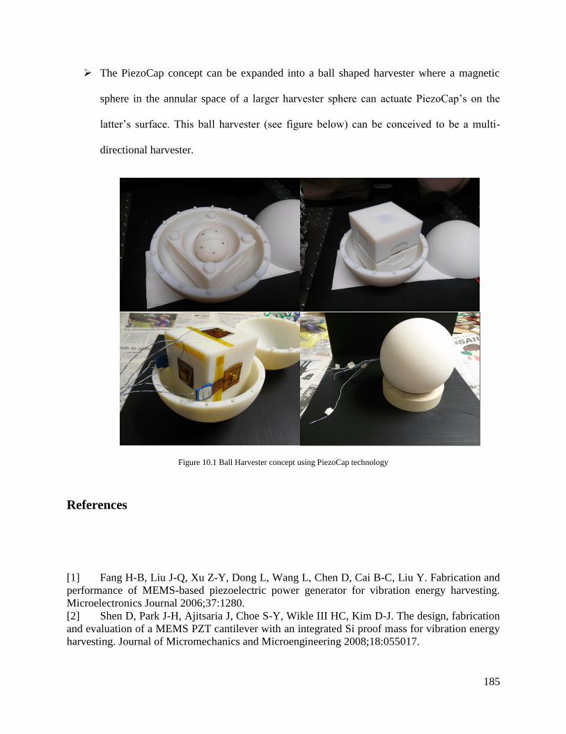
185
The PiezoCap concept can be expanded into a ball shaped harvester where a magnetic
sphere in the annular space of a larger harvester sphere can actuate PiezoCap’s on the
latter’s surface. This ball harvester (see figure below) can be conceived to be a multi-
directional harvester.
Figure 10.1 Ball Harvester concept using PiezoCap technology
References
[1] Fang H-B, Liu J-Q, Xu Z-Y, Dong L, Wang L, Chen D, Cai B-C, Liu Y. Fabrication and
performance of MEMS-based piezoelectric power generator for vibration energy harvesting.
Microelectronics Journal 2006;37:1280.
[2] Shen D, Park J-H, Ajitsaria J, Choe S-Y, Wikle III HC, Kim D-J. The design, fabrication
and evaluation of a MEMS PZT cantilever with an integrated Si proof mass for vibration energy
harvesting. Journal of Micromechanics and Microengineering 2008;18:055017.
186
[3] Lee B, Lin S, Wu W, Wang X, Chang P, Lee C. Piezoelectric MEMS generators
fabricated with an aerosol deposition PZT thin film. Journal of Micromechanics and
Microengineering 2009;19:065014.
[4] Jeon YB, Sood R, Jeong Jh, Kim SG. MEMS power generator with transverse mode thin
film PZT. Sensors and Actuators A: Physical 2005;122:16.
[5] Muralt P, Marzencki M, Belgacem B, Calame F, Basrour S. Vibration Energy Harvesting
with PZT Micro Device. Procedia Chemistry 2009;1:1191.
[6] Elfrink R, Kamel T, Goedbloed M, Matova S, Hohlfeld D, Van Andel Y, Van Schaijk R.
Vibration energy harvesting with aluminum nitride-based piezoelectric devices. Journal of
Micromechanics and Microengineering 2009;19:094005.
[7] Reilly E, Wright P. Modeling, fabrication and stress compensation of an epitaxial thin
film piezoelectric microscale energy scavenging device. Journal of Micromechanics and
Microengineering 2009;19:095014.
[8] Morimoto K, Kanno I, Wasa K, Kotera H. High-efficiency piezoelectric energy
harvesters of c-axis-oriented epitaxial PZT films transferred onto stainless steel cantilevers.
Sensors and Actuators A: Physical 2010;163:428.
[9] Isarakorn D, Briand D, Janphuang P, Sambri A, Gariglio S, Triscone J, Guy F, Reiner J,
Ahn C, De Rooij N. The realization and performance of vibration energy harvesting MEMS
devices based on an epitaxial piezoelectric thin film. Smart Materials and Structures
2011;20:025015.
[10] Kim S-H, Leung A, Koo CY, Kuhn L, Jiang W, Kim D-J, Kingon AI. Lead-free
(Na0.5K0.5)(Nb0.95Ta0.05)O3–BiFeO3 thin films for MEMS piezoelectric vibration energy
harvesting devices. Materials Letters 2012;69:24.
[11] Liu H, Lee C, Kobayashi T, Tay C, Quan C. A new S-shaped MEMS PZT cantilever for
energy harvesting from low frequency vibrations below 30 Hz. Microsystem Technologies
2012;18:497.
[12] Liu H, Lee C, Kobayashi T, Tay CJ, Quan C. Piezoelectric MEMS-based wideband
energy harvesting systems using a frequency-up-conversion cantilever stopper. Sensors and
Actuators A: Physical 2012;186:242.
[13] Aktakka EE, Peterson RL, Najafi K. A self-supplied inertial piezoelectric energy
harvester with power-management IC. Solid-State Circuits Conference Digest of Technical
Papers (ISSCC), 2011 IEEE International, 2011. p.120.
[14] Hajati A, Kim S-G. Ultra-wide bandwidth piezoelectric energy harvesting. Applied
Physics Letters 2011;99:083105.

187
Chapter 11
Appendix
Other New Technologies and Techniques for Energy Harvesters and Sensors
Magnetoelectric Thin Film Transformer for Sensing
A single layer transformer structure is shown below (Figure 11.1). It consists of a NFO dot over
a patterned Platinum electrode which in turn is over a patterned or unpatterned PZT thin film. A
diffusion barrier layer of Pt also serves as the ground for both input (ring) and output (dot)
electrodes.
Figure 11.1 Schematic of a Single Layer Transformer structure
We have utilized photo etched metal shadow masks to deposit patterned thin films (see Table
11.1 below for process sequence). We also used magnets (shown in blue in Figure 11.2) to
protect the underlying layer’s electrical pads from deposition.

188
Table 11.1 Shadow mask based fabrication process flow
Figure 11.2 Shadow mask processing using metal shadow mask and magnets (to protect electrical pads from deposition)
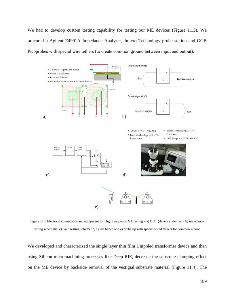
189
We had to develop custom testing capability for testing our ME devices (Figure 11.3). We
procured a Agilent E4991A Impedance Analyzer, Jmicro Technology probe station and GGB
Picoprobes with special wire tethers (to create common ground between input and output).
a) b)
c) d)
e)
Figure 11.3 Electrical connections and equipment for High Frequency ME testing – a) DUT (device under test), b) impedance
testing schematic, c) Gain testing schematic, d) test bench and e) probe tip with special wired tethers for common ground
We developed and characterized the single layer thin film Unipoled transformer device and then
using Silicon micromachining processes like Deep RIE, decrease the substrate clamping effect
on the ME device by backside removal of the vestigial substrate material (Figure 11.4). The
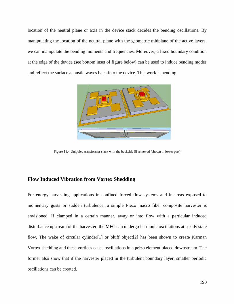
190
location of the neutral plane or axis in the device stack decides the bending oscillations. By
manipulating the location of the neutral plane with the geometric midplane of the active layers,
we can manipulate the bending moments and frequencies. Moreover, a fixed boundary condition
at the edge of the device (see bottom inset of figure below) can be used to induce bending modes
and reflect the surface acoustic waves back into the device. This work is pending.
Figure 11.4 Unipoled transformer stack with the backside Si removed (shown in lower part)
Flow Induced Vibration from Vortex Shedding
For energy harvesting applications in confined forced flow systems and in areas exposed to
momentary gusts or sudden turbulence, a simple Piezo macro fiber composite harvester is
envisioned. If clamped in a certain manner, away or into flow with a particular induced
disturbance upstream of the harvester, the MFC can undergo harmonic oscillations at steady state
flow. The wake of circular cylinder[1] or bluff object[2] has been shown to create Karman
Vortex shedding and these vortices cause oscillations in a peizo element placed downstream. The
former also show that if the harvester placed in the turbulent boundary layer, smaller periodic
oscillations can be created.

191
A flow disturbance was created upstream of the harvester by a flat plate (Figure 11.5) - a)
positioned 45 degrees to the wall of the wind tunnel or b) rotated from 90 degrees to -90 degrees
in 1 second. Wind speed was maintained at 16 mps or 36 mph. The different configurations
tested are as follows: 1) Piezo MFC is facing into the flow or away from flow (shown below), 2)
an L-shaped metal piece was attached to MFC to create eddies, 3) ‘Perpendicular’ was MFC
perpendicular to flow, 4) ‘Blocking’ flow mode and 5) ‘Parallel’ was MFC parallel to flow
(shown below).
Figure 11.5 Configuration of Piezo MFC parallel to wind tunnel with free end away from flow
The results are summarized below for the 45 degree plate (Figure 11.6):

192
Figure 11.6 Results of a Piezo MFC with a 45 degree plate upstream (clockwise from top left): Comparison between P1 d33 and
P2 type d31MFC’s, Dominant frequencies for P1 vs. P2 vs. orientation and typical Voltage FRF
For the rotating plate condition, the results were less spectacular (Figure 11.7) but still
demonstrate applications where random sudden gusts of flow are common.
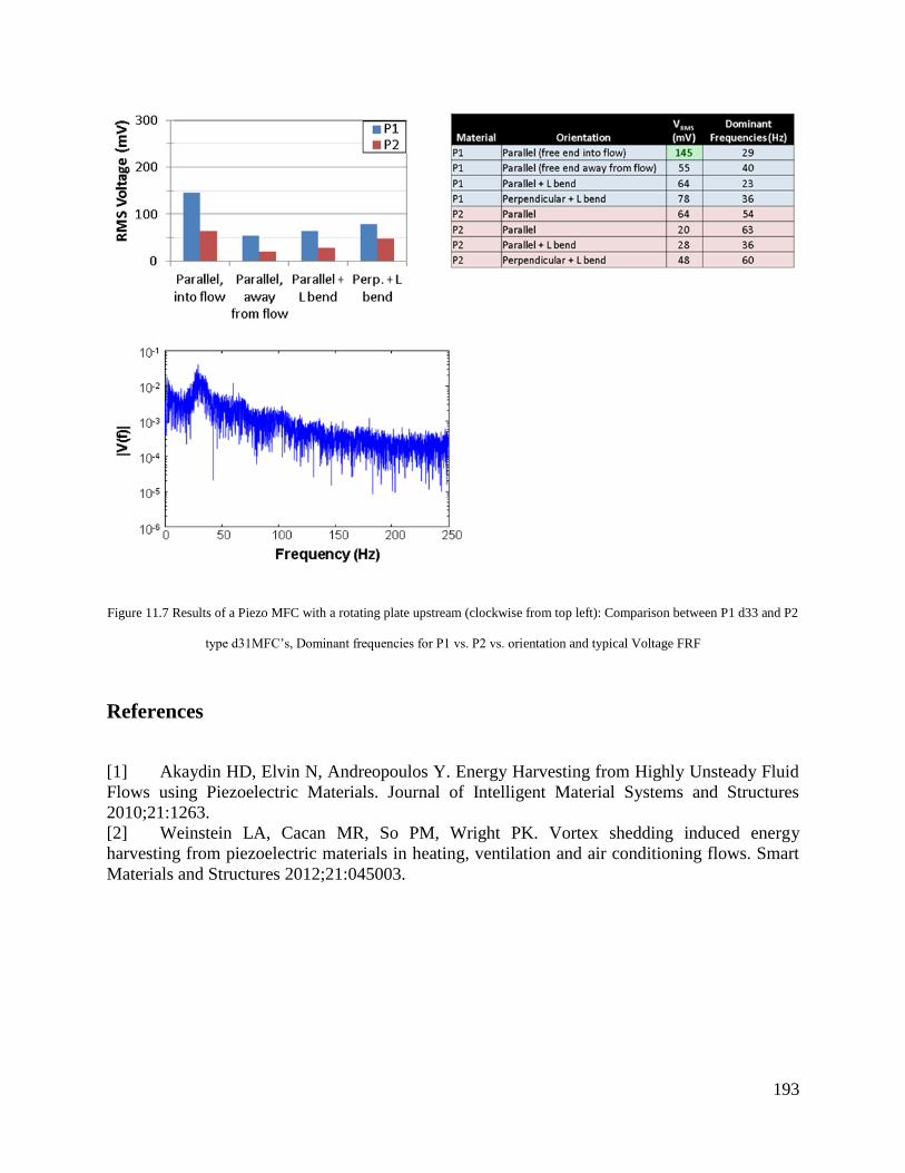
193
Figure 11.7 Results of a Piezo MFC with a rotating plate upstream (clockwise from top left): Comparison between P1 d33 and P2
type d31MFC’s, Dominant frequencies for P1 vs. P2 vs. orientation and typical Voltage FRF
References
[1] Akaydin HD, Elvin N, Andreopoulos Y. Energy Harvesting from Highly Unsteady Fluid
Flows using Piezoelectric Materials. Journal of Intelligent Material Systems and Structures
2010;21:1263.
[2] Weinstein LA, Cacan MR, So PM, Wright PK. Vortex shedding induced energy
harvesting from piezoelectric materials in heating, ventilation and air conditioning flows. Smart
Materials and Structures 2012;21:045003.
Related Documents