1 Microstereolithography Prasanna S. Gandhi Assistant Professor, Department of Mechanical Engineering, Indian Institute of Technology, Bombay, MEMS: Fabrication:

Welcome message from author
This document is posted to help you gain knowledge. Please leave a comment to let me know what you think about it! Share it to your friends and learn new things together.
Transcript

1
Microstereolithography
Prasanna S. GandhiAssistant Professor,Department of Mechanical Engineering,Indian Institute of Technology, Bombay,
MEMS: Fabrication:

2
Recap
Optical characterizationPrevious classes on fabrication
VLSI based methodsPatterningEtchingDeposition
EDMECMLaser machining

3
Today’s Class
MicrostereolithographyAdvantagesFundamentals of laser opticsMethods
Projection methodScanning method
Some fundamentals of polymerization
4
What is Microstereolithography?
Novel microfabrication process for fabricating high aspect ratio and complex 3D microstructures.Evolved from the rapid
prototyping industry.UV laser beam scanned on a
photopolymerizable resin.Curing of the resin layer by
layer.Stacking of all the layers.

5
Need for MicrostereolithographyMEMS – Worldwide Research attentionRequirement of current actuating and sensing
mechanisms to be of complex 3D shapes.Incorporation of a wide range of materials
Limitations of Conventional processes :Inability to manufacture high aspect ratio and complex
3D microstructures.Few semiconductors and other materials processed by
current VLSI-based machining processes for MEMS.
Motivation

6
Microstereolithography
Scanning method:Scan one layer by focused laser beam and then the next layer
Dynamic mask method:Expose the layer to be built at a time Change the mask dynamically Expose the next layer
Process Types

7
Scanning Method
Classical mslFocusing by a dynamic lensUse of galvanometric mirrorsTheoretical best point of focus not intersecting the resin surface.
Free surface techniqueAll optical parts fixedX-Y-Z motorized translation stageThickness control of deposited liquid layer difficult

8
Schematic diagram
Laser
Mirror
Elevatorz
Laser curablephotopolymer
Vector Scan
Scanning Method

9
Factors affecting resolution of components:Laser intensityMotion and quality of the beamPhotopolymer/ monomer usedFocusingExposure
In case of ceramic materials process of laser sintering is used
Issues
Scanning Method

10
Scanning Method
1. Fixed optics, move liquid tank for xyscanning
2. Various ways for scanning- Rotating galvano-scanning mirrors- Linearly moving mirrors- Raster scan vs vector scan
Variations

11
MicrostereolithographyMicrostereolithographyDynamic mask process
DynamicMask
Laser curablephotopolymer
Elevetorz
Dynamically changing mask according to the section to be exposedComputer

12
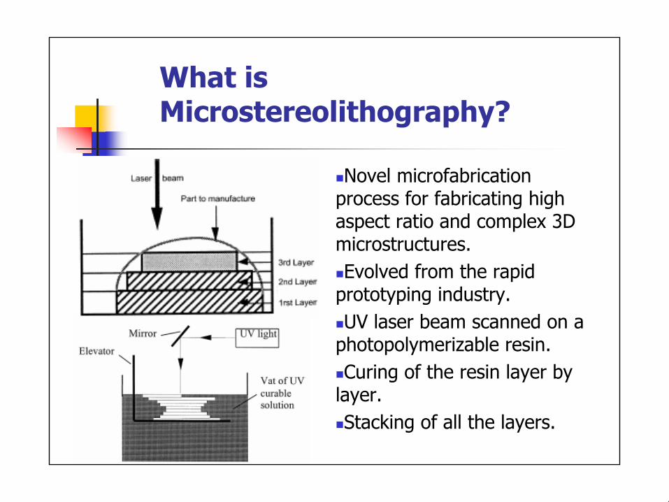
Fundamentals of Laser Beam
Gaussian BeamsBeam waist at z = 0, where the spot size is w0.Expansion to w = w(z) with distance z away from the laser. The beam radius of curvature, R(z), also increases with distance far away.
13
Fundamentals of Laser Beam
where zR is the Rayleigh Range (the distance over which the beam remains about the same diameter), and it's given by:
Expressions for spot size, radius of curvature,

14
Fundamentals of Laser Beam
Gaussian Beam Focusing
Airy Disk formula for spot size:

15
System Details
Typical System ComponentsLaserBeam delivery systemComputer controlled precision stages and a
CAD design toolProcess monitoring system with a CCD camera.UV curable resin – HDDA (1,6 – Hexanediol
diacrylate)

16
Laser
UV LampsHe-Cd LaserArgon Ion Laser
Typical specifications :Name of the supplier : Coherent Inc. Product model : Innova 300 Series (I-304) (Ar+ Laser)Multiline UV wavelengths : 333.4nm to 363.8nm Power : 200mW Diameter (@ 1/e2 points) in mm : 1.5mm Divergence (full angle) in mrad : 0.5
17
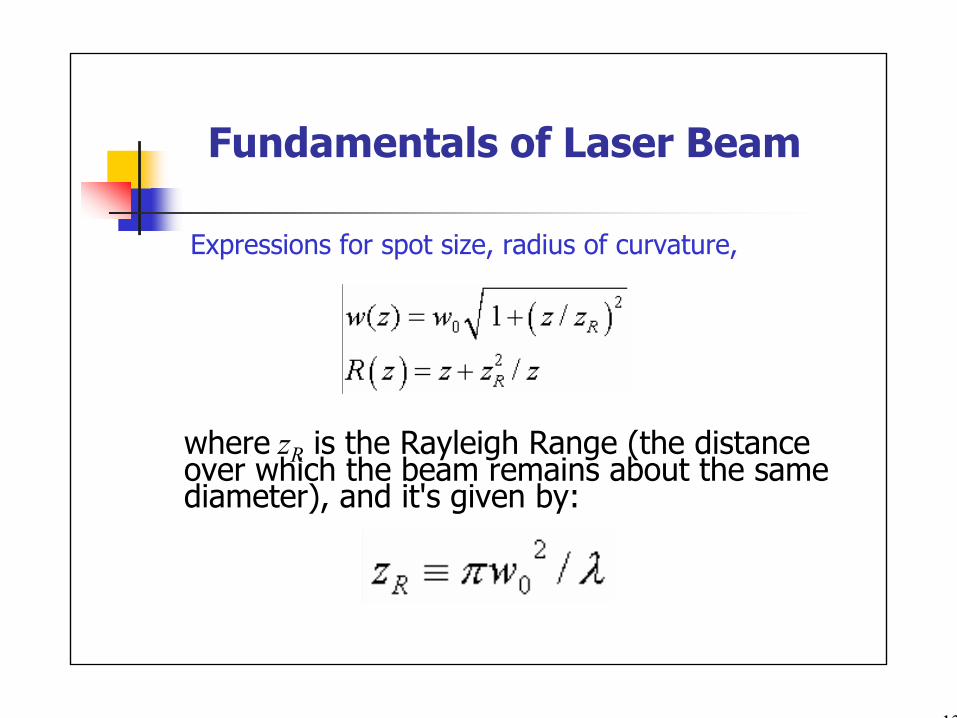
UV- curable Resin
Desired Properties:-Photosensitivity at the operating wavelengthLow viscosity to produce a smooth surfaceHigh curing speedLow shrinkage during polymerizationHigh absorption for low penetration of light.
Types of Resins1)Epoxy Resins2)Acrylate resinsHDDA (1,6 – Hexanediol diacrylate) with 4% by wt. photoinitiator

18
Spot characterization using Oslo

19
Mathematical Modeling
Laser exposure along the X-Axis defined as
Cured Line width:
Curing depth working equation :

20
Mathematical ModelingLaser exposure along the X-Axis defined as

21
Microstereolithography
Smooth 3D surfaces difficult to produce; stepping effects will always be presentMass production of several components is another challenge Extremely small features difficult to produce
Limitations

22
Conclusions
Microstereolithography: process detailsMainly a process for true 3D structures of polymer and ceramic materialsLimitation about the size of the feature
Any suggestions to improveE-beam with z-stage movement

23
Mathematical Modeling
Off-Axis BeamExposure (Energy per unit area)
Line Spread Function (LSF)
Modified expression for exposure:
Related Documents