Memory Taken from Digital Design and Computer Architecture by Harris and Harris and Computer Organization and Architecture by Null and Lobur

Memory Taken from Digital Design and Computer Architecture by Harris and Harris and Computer Organization and Architecture by Null and Lobur.
Dec 21, 2015
Welcome message from author
This document is posted to help you gain knowledge. Please leave a comment to let me know what you think about it! Share it to your friends and learn new things together.
Transcript

Memory
Taken from Digital Design and Computer Architecture by Harris and
Harris and Computer Organization and Architecture by Null and Lobur

Copyright © 2007 Elsevier 7-<2>
Single-Cycle Processor
SignImm
CLK
A RD
InstructionMemory
+
4
A1
A3
WD3
RD2
RD1WE3
A2
CLK
Sign Extend
RegisterFile
0
1
0
1
A RD
DataMemory
WD
WE0
1
PC0
1PC' Instr
25:21
20:16
15:0
5:0
SrcB
20:16
15:11
<<2
+
ALUResult ReadData
WriteData
SrcA
PCPlus4
PCBranch
WriteReg4:0
Result
31:26
RegDst
Branch
MemWrite
MemtoReg
ALUSrc
RegWrite
Op
Funct
ControlUnit
Zero
PCSrc
CLK
ALUControl2:0
ALU
Copyright © 2007 Elsevier 5-<3>
Memory Arrays
Address
Data
ArrayN
M
• Efficiently store large amounts of data
• Three common types:– Dynamic random access memory (DRAM)
– Static random access memory (SRAM)
– Read only memory (ROM)
• An M-bit data value can be read or written at each unique N-bit address.

Copyright © 2007 Elsevier 5-<4>
• Two-dimensional array of bit cells
• Each bit cell stores one bit
• An array with N address bits and M data bits:– 2N rows and M columns
– Depth: number of rows (number of words)
– Width: number of columns (size of word)
– Array size: depth × width = 2N × M
Memory Arrays
Address
Data
ArrayN
M
Address Data
11
10
01
00
depth
0 1 0
1 0 0
1 1 0
0 1 1
width
Address
Data
Array2
3

Copyright © 2007 Elsevier 5-<5>
• 22 × 3-bit array
• Number of words: 4
• Word size: 3-bits
• For example, the 3-bit word stored at address 10 is 100
Memory Array: Example
Example:Address Data
11
10
01
00
depth
0 1 0
1 0 0
1 1 0
0 1 1
width
Address
Data
Array2
3
Copyright © 2007 Elsevier 5-<6>
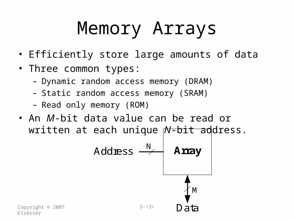
Memory Arrays
Address
Data
1024-word x32-bitArray
10
32
Copyright © 2007 Elsevier 5-<7>
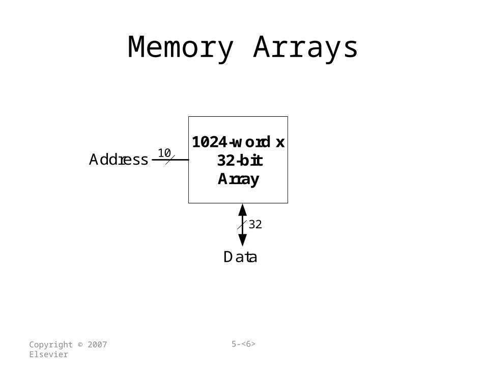
Memory Array Bit Cells
stored bit
wordline
bitline
Example:
stored bit = 0
wordline = 1
stored bit = 1
stored bit = 0
stored bit = 1
bitline =
(a) (b)
wordline = 1
wordline = 0
wordline = 0
bitline =
bitline =
bitline =

Copyright © 2007 Elsevier 5-<8>
Memory Array Bit Cells
stored bit
wordline
bitline
Example:
stored bit = 0
wordline = 1
stored bit = 1
stored bit = 0
stored bit = 1
bitline =
(a) (b)
wordline = 1
wordline = 0
wordline = 0
bitline =
bitline =
bitline =0
1
Z
Z
Copyright © 2007 Elsevier 5-<9>
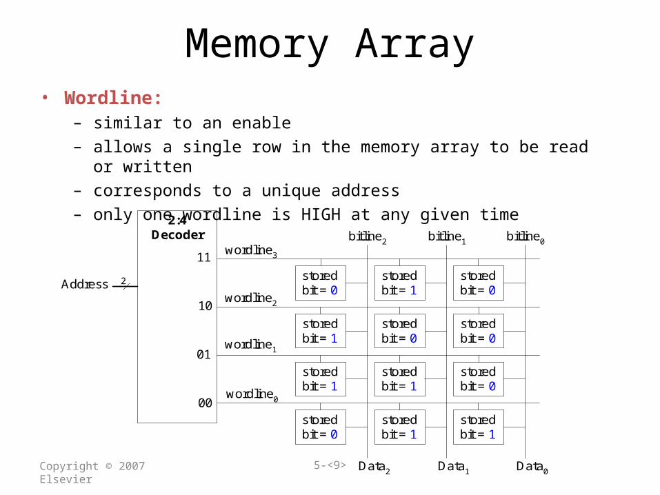
• Wordline: – similar to an enable
– allows a single row in the memory array to be read or written
– corresponds to a unique address
– only one wordline is HIGH at any given time
Memory Array
wordline311
10
2:4Decoder
Address
01
00
storedbit = 0
wordline2
wordline1
wordline0
storedbit = 1
storedbit = 0
storedbit = 1
storedbit = 0
storedbit = 0
storedbit = 1
storedbit = 1
storedbit = 0
storedbit = 0
storedbit = 1
storedbit = 1
bitline2 bitline1 bitline0
Data2 Data1 Data0
2

Copyright © 2007 Elsevier 5-<10>
Types of Memory
• Random access memory (RAM): volatile• Read only memory (ROM): nonvolatile
Copyright © 2007 Elsevier 5-<11>
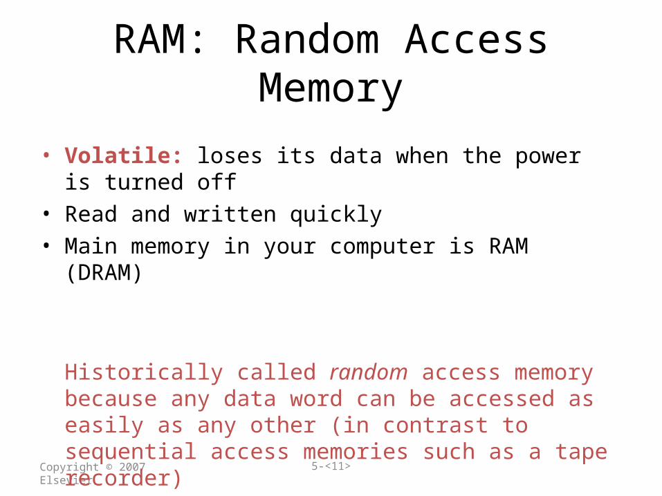
RAM: Random Access Memory
• Volatile: loses its data when the power is turned off
• Read and written quickly
• Main memory in your computer is RAM (DRAM)
Historically called random access memory because any data word can be accessed as easily as any other (in contrast to sequential access memories such as a tape recorder)

Copyright © 2007 Elsevier 5-<12>
ROM: Read Only Memory
• Nonvolatile: retains data when power is turned off
• Read quickly, but writing is impossible or slow
• Flash memory in cameras, thumb drives, and digital cameras are all ROMs
Historically called read only memory because ROMs were written at manufacturing time or by burning fuses. Once ROM was configured, it could not be written again. This is no longer the case for Flash memory and other types of ROMs.
Copyright © 2007 Elsevier 5-<13>
Types of RAM
• Two main types of RAM:
– Dynamic random access memory (DRAM)
– Static random access memory (SRAM)
• Differ in how they store data:
– DRAM uses a capacitor
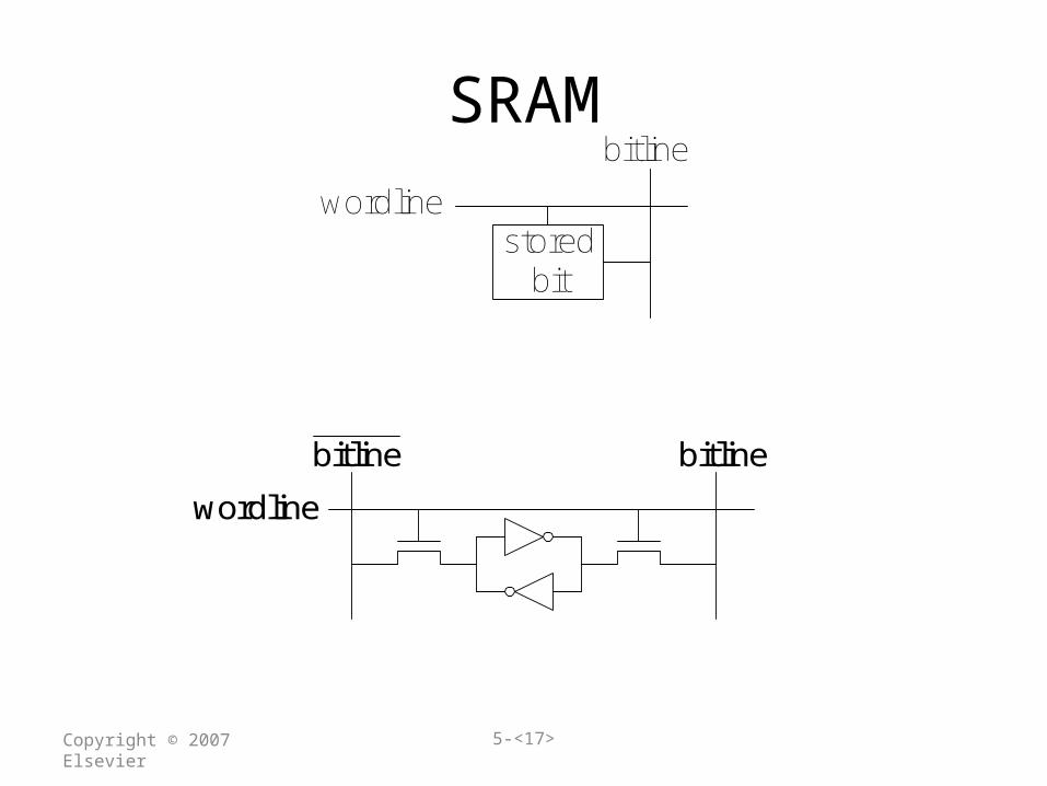
– SRAM uses cross-coupled inverters
Copyright © 2007 Elsevier 5-<14>
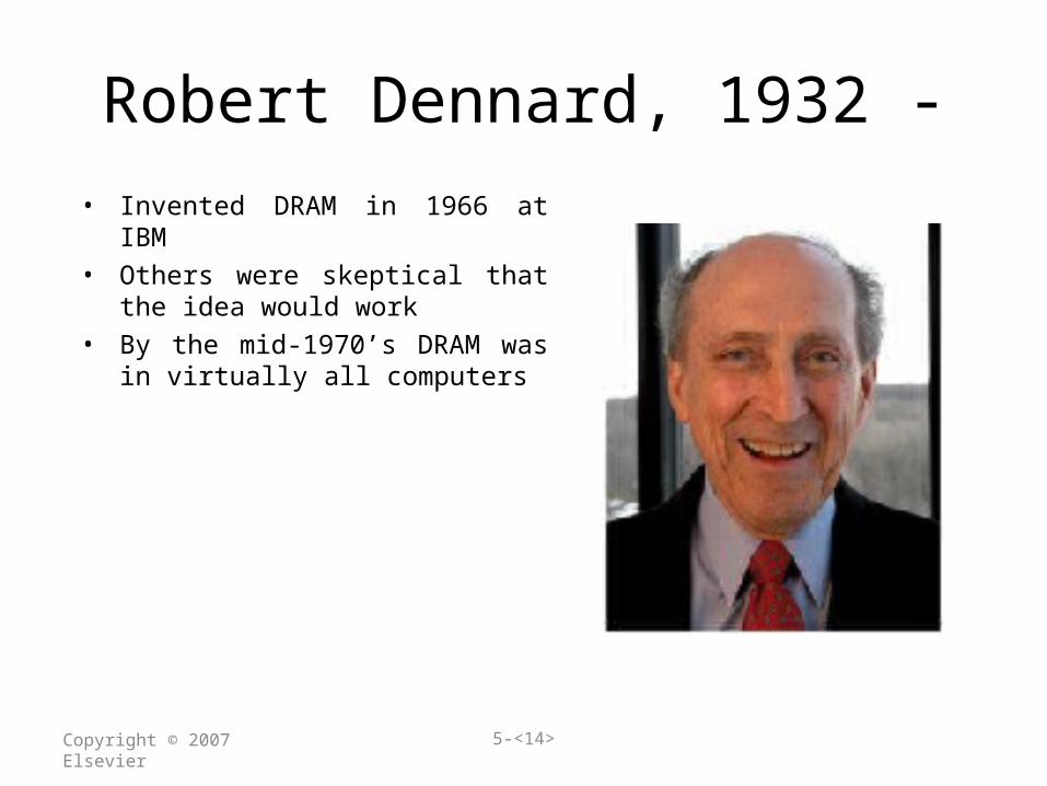
Robert Dennard, 1932 -• Invented DRAM in 1966 at IBM
• Others were skeptical that the idea would work
• By the mid-1970’s DRAM was in virtually all computers
Copyright © 2007 Elsevier 5-<15>
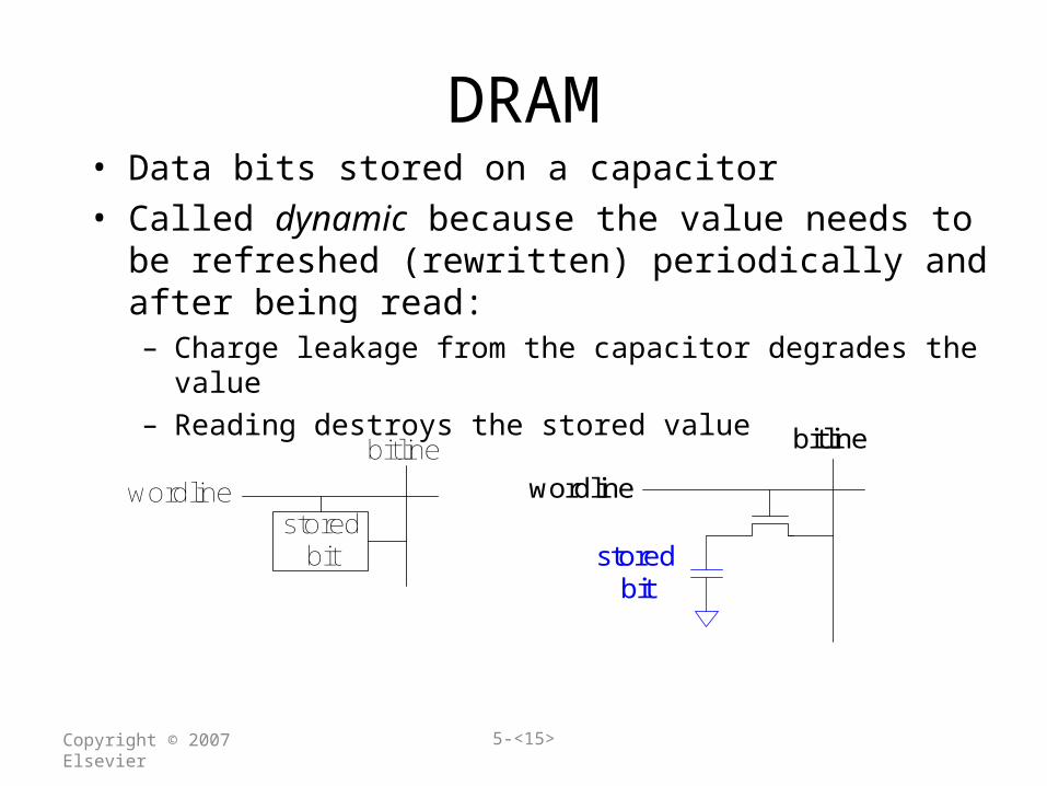
• Data bits stored on a capacitor
• Called dynamic because the value needs to be refreshed (rewritten) periodically and after being read:– Charge leakage from the capacitor degrades the value
– Reading destroys the stored value
DRAM
stored bit
wordline
bitline
wordline
bitline
storedbit

Copyright © 2007 Elsevier 5-<16>
DRAM
wordline
bitline
wordline
bitline
+ +storedbit = 1
storedbit = 0
Copyright © 2007 Elsevier 5-<17>
SRAM
stored bit
wordline
bitline
wordline
bitline bitline

Copyright © 2007 Elsevier 5-<18>
wordline311
10
2:4Decoder
Address
01
00
storedbit = 0
wordline2
wordline1
wordline0
storedbit = 1
storedbit = 0
storedbit = 1
storedbit = 0
storedbit = 0
storedbit = 1
storedbit = 1
storedbit = 0
storedbit = 0
storedbit = 1
storedbit = 1
bitline2 bitline1 bitline0
Data2 Data1 Data0
2
Memory Arrays
wordline
bitline bitlinewordline
bitline
DRAM bit cell: SRAM bit cell:

Copyright © 2007 Elsevier 5-<19>
ROMs: Dot Notation
11
10
2:4 Decoder
Address
Data0Data1Data2
01
00
2
wordline
bitline
wordline
bitline
bit cellcontaining 0
bit cellcontaining 1
To read the cell the bitline is weakly pulled high.

Copyright © 2007 Elsevier 5-<20>
ROM Storage
11
10
2:4 Decoder
Address
Data0Data1Data2
01
00
2
Address Data
11
10
01
00
depth
0 1 0
1 0 0
1 1 0
0 1 1
width
Copyright © 2007 Elsevier 5-<21>
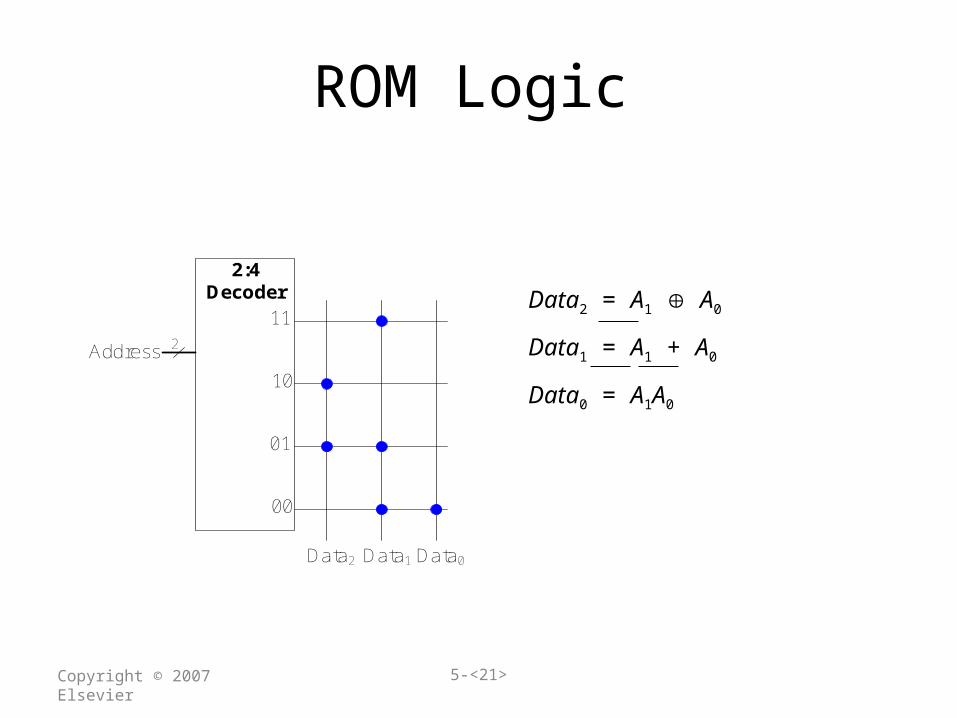
ROM Logic
11
10
2:4 Decoder
Address
Data0Data1Data2
01
00
2
Data2 = A1 A0
Data1 = A1 + A0
Data0 = A1A0
Copyright © 2007 Elsevier 5-<22>
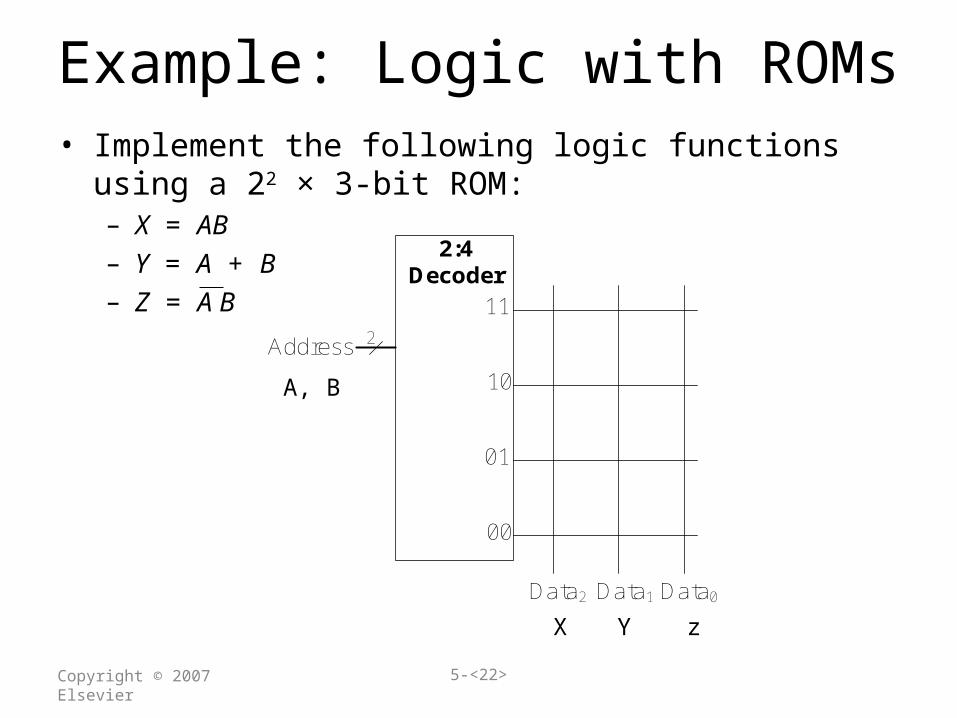
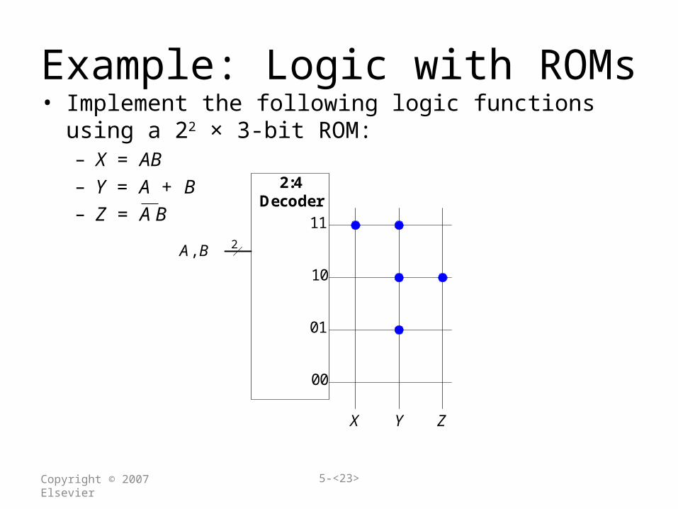
Example: Logic with ROMs
11
10
2:4 Decoder
Address
Data0Data1Data2
01
00
2
• Implement the following logic functions using a 22 × 3-bit ROM:– X = AB
– Y = A + B
– Z = A B
zYX
A, B
Copyright © 2007 Elsevier 5-<23>
Example: Logic with ROMs• Implement the following logic functions using a 22 × 3-bit
ROM:– X = AB
– Y = A + B
– Z = A B 11
10
2:4Decoder
A, B
ZYX
01
00
2

Copyright © 2007 Elsevier 5-<24>
Logic with Memory Arrays• Called lookup tables (LUTs): look up output at each input
combination (address)
storedbit = 1
storedbit = 0
00
01
2:4Decoder
A
storedbit = 0
bitline
storedbit = 0
Y
B
10
11
4-word x 1-bit Array
A B Y0 00 11 01 1
0001
TruthTable
A1
A0
Copyright © 2007 Elsevier 5-<25>
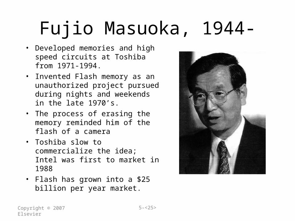
Fujio Masuoka, 1944-• Developed memories and high
speed circuits at Toshiba from 1971-1994.
• Invented Flash memory as an unauthorized project pursued during nights and weekends in the late 1970’s.
• The process of erasing the memory reminded him of the flash of a camera
• Toshiba slow to commercialize the idea; Intel was first to market in 1988
• Flash has grown into a $25 billion per year market.
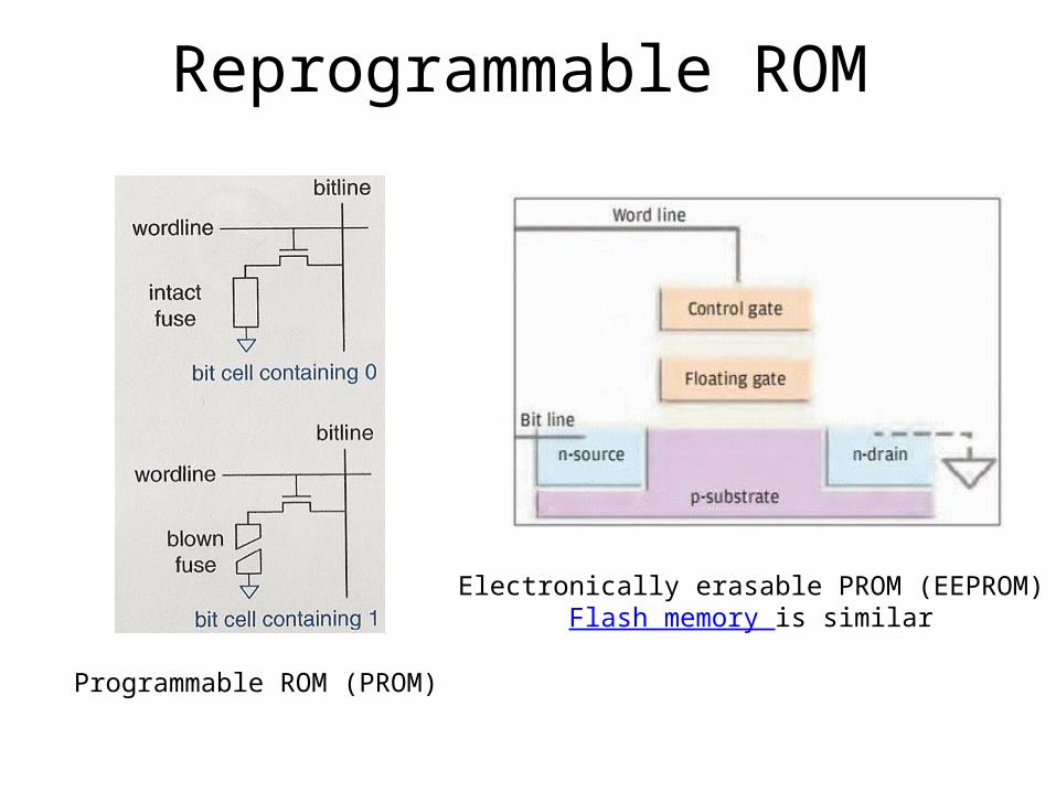
Reprogrammable ROM
Programmable ROM (PROM)
Electronically erasable PROM (EEPROM)Flash memory is similar

Copyright © 2007 Elsevier 5-<27>
Multi-ported Memories
A1
A3
WD3
WE3
A2
CLK
Array
RD2
RD1M
M
N
N
N
M
• Port: address/data pair
• 3-ported memory– 2 read ports (A1/RD1, A2/RD2)
– 1 write port (A3/WD3, WE3 enables writing)
• Small multi-ported memories are called register files

Copyright © 2007 Elsevier 5-<28>
// 256 x 3 memory module with one read/write portmodule mem( input clk, we, input [7:0] a
input [2:0] wd, output [2:0] rd);
reg [2:0] RAM[255:0];
assign rd = RAM[a];
always @(posedge clk) if (we) RAM[a] <= wd;endmodule
Verilog Memory Arrays
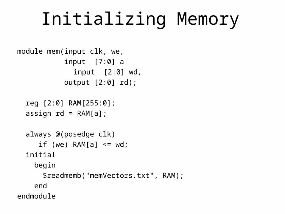
Initializing Memory
module mem(input clk, we, input [7:0] a
input [2:0] wd, output [2:0] rd);
reg [2:0] RAM[255:0]; assign rd = RAM[a];
always @(posedge clk) if (we) RAM[a] <= wd; initial begin $readmemb("memVectors.txt", RAM); endendmodule
Copyright © 2007 Elsevier 5-<30>
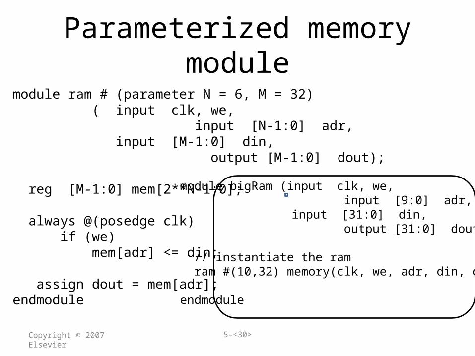
module ram # (parameter N = 6, M = 32) ( input clk, we,
input [N-1:0] adr, input [M-1:0] din,
output [M-1:0] dout);
reg [M-1:0] mem[2**N-1:0];
always @(posedge clk) if (we) mem[adr] <= din;
assign dout = mem[adr];endmodule
Parameterized memory module
module bigRam (input clk, we, input [9:0] adr,
input [31:0] din, output [31:0] dout);
// instantiate the ram ram #(10,32) memory(clk, we, adr, din, dout);
endmodule
31
Memory Organization
• Memory can be byte-addressable, or word-addressable, where a word typically consists of two or more bytes.
• Memory is constructed of RAM chips, often referred to in terms of length width.
32
• Physical memory usually consists of more than one RAM chip.
• Access is more efficient when memory is organized into banks of chips with the addresses interleaved across the chips
• With low-order interleaving, the low order bits of the address specify which memory bank contains the address of interest.
• Accordingly, in high-order interleaving, the high order address bits specify the memory bank.
The next slide illustrates these two ideas.
4.6 Memory Organization

33
Low-Order Interleaving
High-Order Interleaving
4.6 Memory Organization
34
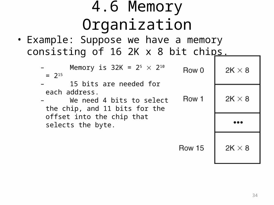
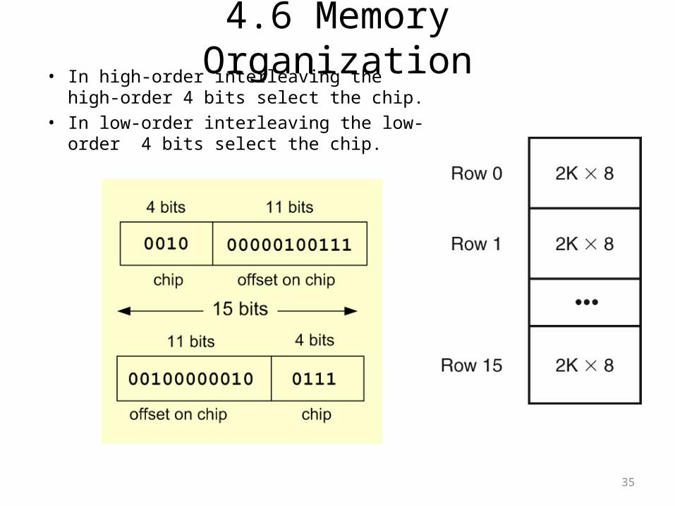
4.6 Memory Organization• Example: Suppose we have a memory consisting of
16 2K x 8 bit chips.
– Memory is 32K = 25 210 = 215
– 15 bits are needed for each address.
– We need 4 bits to select the chip, and 11 bits for the offset into the chip that selects the byte.
35
4.6 Memory Organization• In high-order interleaving the high-order
4 bits select the chip.
• In low-order interleaving the low-order 4 bits select the chip.
Related Documents