Memory expansions for the Commodore 128 Marko Mäkelä Pekka Pessi April 17, 1994 [last essential modification on December 22, 1999] * †‡§ As the Commodore 128 was first introduced, 128 kilobytes feeled like an unbelievably big amount of memory. Nowadays even plain terminals and game consoles have more, and you can easily expand even a Commodore 64 to 256 kilobytes, twice as much as its big brother has by default. There are several commercial memory expansions for the Commodores 128 and 64, but they are rather expensive, and most if not all of them are not being manufactured any more. This article introduces three different memory expansions for the Commodore 128 and 128D computers. With these instructions, you can expand your computer to 256, 512 or 1024 kilobytes of internal memory. The 1024 kilobyte expansion is actually a combination of the two former ones, and it is fully compatible with both of them. When built by oneself, the 1024 kB expansion can remain cheaper than 200 Finnish marks. 1 I set three goals to the expansions. The bigger expansions should be fully compatible with the internal 256 kB expansion for the Commodore 64 when the computer is in C64 mode, and the 256 kB and 1024 kB expansions should be downwards compatible with a commercial internal 256 kB expansion for the Commodore 128. Finally, an expanded computer should be fully downwards compatible with an unexpanded one. The design aims to a hardware that supports programming. The 256 kB and 1 MB expansions enhance the capabil- ities of the MMU in a way that the engineers at Commodore must have planned, and the other memory management logic is even easier to program. * This document is partially based on Pekka Pessi’s two articles describing an 256 kB internal memory expansion for the Commodore 64. The articles were originally published in the largest Nordic and Finnish home computer users’ magazine, MikroBITTI, in its first two issues in the year 1987. Six years later, they were translated to English and edited by Marko Mäkelä, with help from Pekka Pessi. † August 1996: Thanks to Wolfgang Scherr from Austria, who noticed my mistake in the schematic diagram. The inputs of the 74LS153 chip were mixed, which caused the address block decoding to fail. ‡ December 1999: By now, I know of two 64s and four 128s where this expansion has been built. The expansion never became a success, although the banked concept is technically better than the Commodore REU. § January 2006: Thanks to Marco van den Heuvel, who implemented the expansion in the emulator VICE 1.19, for pointing out errors in the first sample code for initializing the PIA. 1 One Americal dollar (USD) is equivalent to five or six Finnish marks (FIM). My expansion costed about 240 FIM, but I bought some parts in vain, and could have bought the (second-hand) memory chips somewhat cheaper. This time they costed 117 FIM. 1

Welcome message from author
This document is posted to help you gain knowledge. Please leave a comment to let me know what you think about it! Share it to your friends and learn new things together.
Transcript
Memory expansions for the Commodore 128
Marko Mäkelä Pekka Pessi
April 17, 1994[last essential modification on December 22, 1999]∗†‡§
As the Commodore 128 was first introduced, 128 kilobytes feeled like an unbelievably big amount of memory.Nowadays even plain terminals and game consoles have more, and you can easily expand even a Commodore 64 to256 kilobytes, twice as much as its big brother has by default.
There are several commercial memory expansions for the Commodores 128 and 64, but they are rather expensive,and most if not all of them are not being manufactured any more.
This article introduces three different memory expansions for the Commodore 128 and 128D computers. Withthese instructions, you can expand your computer to 256, 512 or 1024 kilobytes of internal memory. The 1024kilobyte expansion is actually a combination of the two former ones, and it is fully compatible with both of them.When built by oneself, the 1024 kB expansion can remain cheaper than 200 Finnish marks.1
I set three goals to the expansions. The bigger expansions should be fully compatible with the internal 256 kBexpansion for the Commodore 64 when the computer is in C64 mode, and the 256 kB and 1024 kB expansions shouldbe downwards compatible with a commercial internal 256 kB expansion for the Commodore 128. Finally, an expandedcomputer should be fully downwards compatible with an unexpanded one.
The design aims to a hardware that supports programming. The 256 kB and 1 MB expansions enhance the capabil-ities of the MMU in a way that the engineers at Commodore must have planned, and the other memory managementlogic is even easier to program.
∗This document is partially based on Pekka Pessi’s two articles describing an 256 kB internal memory expansion for the Commodore 64. Thearticles were originally published in the largest Nordic and Finnish home computer users’ magazine, MikroBITTI, in its first two issues in the year1987. Six years later, they were translated to English and edited by Marko Mäkelä, with help from Pekka Pessi.
†August 1996: Thanks to Wolfgang Scherr from Austria, who noticed my mistake in the schematic diagram. The inputs of the 74LS153 chipwere mixed, which caused the address block decoding to fail.
‡December 1999: By now, I know of two 64s and four 128s where this expansion has been built. The expansion never became a success,although the banked concept is technically better than the Commodore REU.
§January 2006: Thanks to Marco van den Heuvel, who implemented the expansion in the emulator VICE 1.19, for pointing out errors in the firstsample code for initializing the PIA.
1 One Americal dollar (USD) is equivalent to five or six Finnish marks (FIM). My expansion costed about 240 FIM, but I bought some parts invain, and could have bought the (second-hand) memory chips somewhat cheaper. This time they costed 117 FIM.
1
Contents1 Some basics 3
1.1 Expansion memory in 16 kB blocks . . . . . . . . . . . . . . . . . . . . . . . . . . . . . . . . . . . 31.2 Memory chips . . . . . . . . . . . . . . . . . . . . . . . . . . . . . . . . . . . . . . . . . . . . . . . 31.3 Dynamic headaches . . . . . . . . . . . . . . . . . . . . . . . . . . . . . . . . . . . . . . . . . . . . 51.4 Memory refresh . . . . . . . . . . . . . . . . . . . . . . . . . . . . . . . . . . . . . . . . . . . . . . 51.5 The MMU expansion . . . . . . . . . . . . . . . . . . . . . . . . . . . . . . . . . . . . . . . . . . . 6
2 Building the expansion 62.1 Disclaimer . . . . . . . . . . . . . . . . . . . . . . . . . . . . . . . . . . . . . . . . . . . . . . . . . 62.2 Getting started . . . . . . . . . . . . . . . . . . . . . . . . . . . . . . . . . . . . . . . . . . . . . . . 62.3 Expanding to 512 kilobytes . . . . . . . . . . . . . . . . . . . . . . . . . . . . . . . . . . . . . . . . 7
2.3.1 Removing the old memory chips . . . . . . . . . . . . . . . . . . . . . . . . . . . . . . . . . 92.3.2 Adding the new address line . . . . . . . . . . . . . . . . . . . . . . . . . . . . . . . . . . . 92.3.3 Prepare for the final step . . . . . . . . . . . . . . . . . . . . . . . . . . . . . . . . . . . . . 102.3.4 Testing . . . . . . . . . . . . . . . . . . . . . . . . . . . . . . . . . . . . . . . . . . . . . . 11
2.4 Expanding to 256 or 1024 kilobytes . . . . . . . . . . . . . . . . . . . . . . . . . . . . . . . . . . . 112.4.1 Realizing the processor bus interface . . . . . . . . . . . . . . . . . . . . . . . . . . . . . . . 142.4.2 Adding the new memory banking signals . . . . . . . . . . . . . . . . . . . . . . . . . . . . 152.4.3 Soldering the memory chips . . . . . . . . . . . . . . . . . . . . . . . . . . . . . . . . . . . 15
3 Using the expansion 153.1 The operation of the block switcher . . . . . . . . . . . . . . . . . . . . . . . . . . . . . . . . . . . 15
3.1.1 PIA’s location in address space . . . . . . . . . . . . . . . . . . . . . . . . . . . . . . . . . . 163.1.2 Block selection . . . . . . . . . . . . . . . . . . . . . . . . . . . . . . . . . . . . . . . . . . 163.1.3 Interfacing the second MMU . . . . . . . . . . . . . . . . . . . . . . . . . . . . . . . . . . . 163.1.4 Startup settings for the PIA expansion . . . . . . . . . . . . . . . . . . . . . . . . . . . . . . 17
3.2 Segmented memory . . . . . . . . . . . . . . . . . . . . . . . . . . . . . . . . . . . . . . . . . . . . 173.3 Critical addresses for the PIA expansion . . . . . . . . . . . . . . . . . . . . . . . . . . . . . . . . . 173.4 Initializing the PIA expansion . . . . . . . . . . . . . . . . . . . . . . . . . . . . . . . . . . . . . . 193.5 Programming the PIA in machine language . . . . . . . . . . . . . . . . . . . . . . . . . . . . . . . 20
3.5.1 An exception: video memory . . . . . . . . . . . . . . . . . . . . . . . . . . . . . . . . . . . 203.6 Programming the MMU . . . . . . . . . . . . . . . . . . . . . . . . . . . . . . . . . . . . . . . . . 213.7 Hints for programming in C128 mode Machine Language . . . . . . . . . . . . . . . . . . . . . . . . 243.8 Programming in C128 mode BASIC . . . . . . . . . . . . . . . . . . . . . . . . . . . . . . . . . . . 26
4 Programming the expansion in C64 mode BASIC 264.1 Processing a huge array . . . . . . . . . . . . . . . . . . . . . . . . . . . . . . . . . . . . . . . . . . 274.2 Storing graphics . . . . . . . . . . . . . . . . . . . . . . . . . . . . . . . . . . . . . . . . . . . . . . 27
5 RAM disk and other C64 mode programs 285.1 Memory test . . . . . . . . . . . . . . . . . . . . . . . . . . . . . . . . . . . . . . . . . . . . . . . . 285.2 Poor man’s multitasking . . . . . . . . . . . . . . . . . . . . . . . . . . . . . . . . . . . . . . . . . 285.3 Machine language monitor . . . . . . . . . . . . . . . . . . . . . . . . . . . . . . . . . . . . . . . . 285.4 RAM disk . . . . . . . . . . . . . . . . . . . . . . . . . . . . . . . . . . . . . . . . . . . . . . . . . 28
5.4.1 Disk copiers . . . . . . . . . . . . . . . . . . . . . . . . . . . . . . . . . . . . . . . . . . . 30
6 Enhancing the PIA expansion 306.1 Built-in freezer . . . . . . . . . . . . . . . . . . . . . . . . . . . . . . . . . . . . . . . . . . . . . . 306.2 New operating system . . . . . . . . . . . . . . . . . . . . . . . . . . . . . . . . . . . . . . . . . . . 31
2
1 Some basicsThis article describes two memory expansions: an expansion that adds two new memory banks to the Commodore 128,doubling its memory space, and another expansion which expands each bank to 256 kilobytes, quadrupling the memoryspace. The former is the 256 kB expansion, from here on the MMU expansion, and the latter is the 512 kB expansion,or the PIA expansion. Combining these two expansions gives you four banks of 256 kilobytes each, that is 1024kilobytes.
When I made the 256 kB expansion to my Commodore 64, I renamed the computer to 2564 — 256 kB C64. Thefirst three digits specify the amount of memory, whereas the last two ones tell the machine type number. A logicalchoice for the name of a 512 kB C128 is 5128 — the first three digits tell the amount of memory in kilobytes, and thelast three expose the original machine type. Unfortunately the 256 kB and 1024 kB expansions for the C128 cannotbe named so nicely. I have baptized my C128D to C1028D, though.
The subsections 1.1 through 1.4 of this section apply for the PIA expansion. You can skip them, if you want tosave some trouble and money and are going to expand your machine only to 256 kilobytes. Similarly, the section 1.5can be skipped if you aim only to the 512 kilobyte expansion.
1.1 Expansion memory in 16 kB blocksThe processor of Commodore 128, MOS 8502, has an 8-bit data bus, and its address bus is 16 bits wide. Like other8-bit processors, it can address only 64 kB of memory at a time. In most 8-bit computers, the memory is limited tothese 64 kilobytes. How could one add memory above this limit?
The solution is simple: the memory is divided into banks of no more than 64 kB, which are switched on and off.Some processors have been added a special circuit for this purpose, in which case the executing program can be in itsown 64 kB bank and the processed data in another bank. For example, MOS 6509, a fellow processor of MOS 8502,works in this way, enabling access to one megabyte. The Commodore 128 uses a sophisticated chip, MOS 8722 MMU(Memory Management Unit), which lets you to activate one 64 kB memory bank of a total of two memory banks at atime.
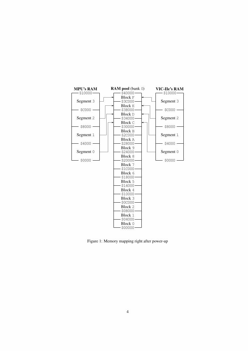
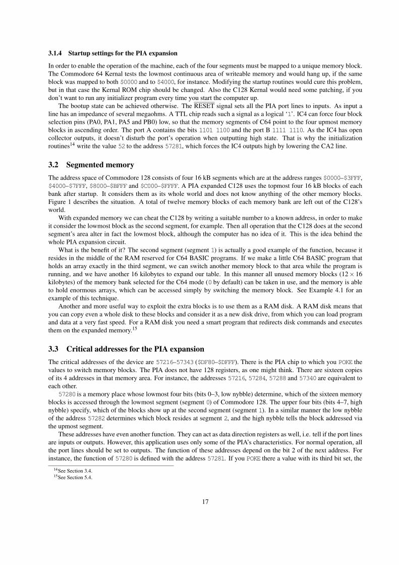
The PIA expansion expands each C128 memory bank to 256 kilobytes. The extended memory is divided to sixteenblocks of sixteen kilobytes each. The processor can address up to four of them at a time. Every four 16 kB segment ofthe address space can be mapped to any 16 kB block. Figure 1 shows the mapping right after startup.
However, the video chip VIC-IIe — MOS 85662 — retrieves its data from the memory outside the normal bus. Theinternal address registers of VIC-IIe are 14 bits wide, so it can address only 16 kB without external logic. The requiredtwo extra bits for accessing the whole 64 kB video bank are provided from the second CIA chip, and the video bankis selected by the MMU. Our extra logic provides additional two address bits for accessing the whole 256 kB of theselected video memory bank.
1.2 Memory chipsCommodore 128 uses 64 kb dynamic RAM chips of JEDEC standard. In 1982, when the Commodore 64 was in-troduced, they were most modern technology, they needed only one operating voltage supply instead of traditionalthree.
The semiconductor memories have developed fast, however, and now a chip in a DIP of equal size can hold 256kilobits. The pinout of these 256 kb chips differs minimally from the 64 kb ones. The smaller 64 kb chips, at least theones used in C64 and C128, have one unused contact. The address line to handle three times bigger memory is tied tothis pin. In the DRAMs the address lines are multiplexed: two address bits use the same pin successively.
In the MikroBITTI article Pekka wrote that 256 kb chips are rather cheap, and the price would lower as theproduction rate increases. Nowadays the production must have almost stopped. When Pekka bought his chips betweenMarch and April of 1986, they costed about 50 FIM each. When the original article was published, they costed lessthan 20 FIM. After that the prices rose due to a memory shortage. But nowadays the chips don’t cost practicallyanything, if you’re lucky. Many users of IBM PC compatibles want to upgrade their system memory with 1 Mb chipsor alike and would like to get rid of their old 256 kb chips. I bought eight second-hand chips with total 35 FIM, andlater 36 chips with 117 FIM, including shipping. The lowest price of unused chip I encountered was 13 FIM a pieceand the highest was 30 FIM, almost 10 times the price I paid!
28564 for NTSC
3
RAM pool (bank 0)MPU’s RAM VIC-IIe’s RAM
-
-
-
-
¾
¾
¾
¾
$00000
$04000
$08000
$0C000
$10000
$14000
$18000
$1C000
$20000
$24000
$28000
$2C000
$30000
$34000
$38000
$3C000
$40000
$0000
$4000
$8000
$C000
$10000
$0000
$4000
$8000
$C000
$10000
Block 0
Block 1
Block 2
Block 3
Block 4
Block 5
Block 6
Block 7
Block 8
Block 9
Block A
Block B
Block C
Block D
Block E
Block F
Segment 0 Segment 0
Segment 1 Segment 1
Segment 2 Segment 2
Segment 3 Segment 3
Figure 1: Memory mapping right after power-up
4
4164 41256ª ª` `
1 116 162 215 153 314 144 413 135 512 126 611 117 710 108 89 9
NC MA8VSS VSS
D DCAS CASW WQ Q
RAS RASMA6 MA6MA0 MA0MA3 MA3MA2 MA2MA4 MA4MA1 MA1MA5 MA5VDD VDDMA7 MA7
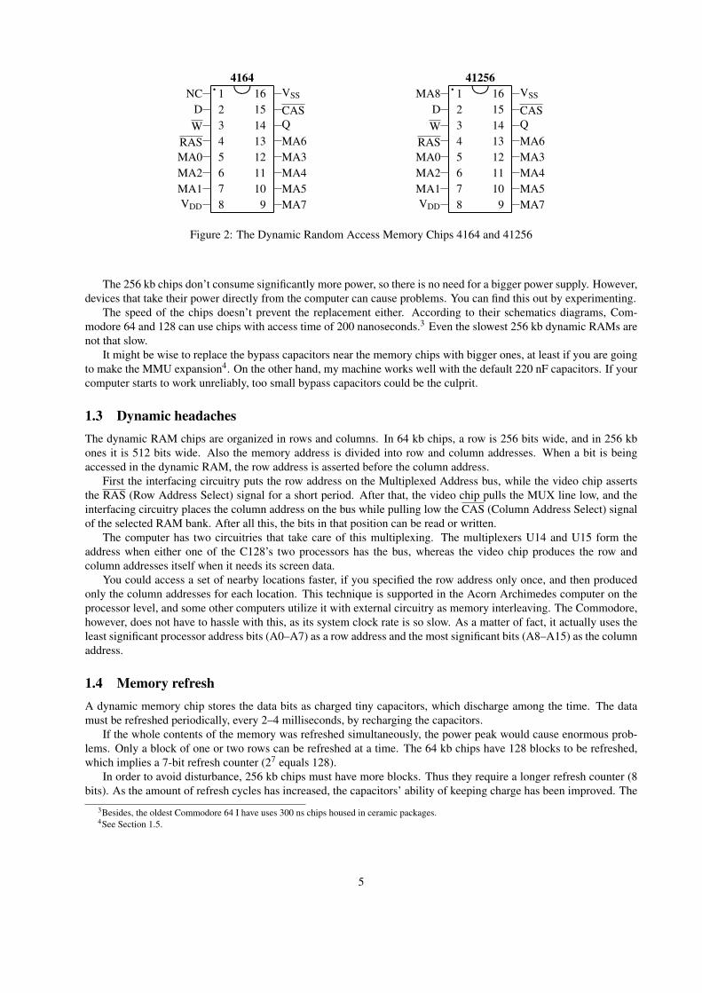
Figure 2: The Dynamic Random Access Memory Chips 4164 and 41256
The 256 kb chips don’t consume significantly more power, so there is no need for a bigger power supply. However,devices that take their power directly from the computer can cause problems. You can find this out by experimenting.
The speed of the chips doesn’t prevent the replacement either. According to their schematics diagrams, Com-modore 64 and 128 can use chips with access time of 200 nanoseconds.3 Even the slowest 256 kb dynamic RAMs arenot that slow.
It might be wise to replace the bypass capacitors near the memory chips with bigger ones, at least if you are goingto make the MMU expansion4. On the other hand, my machine works well with the default 220 nF capacitors. If yourcomputer starts to work unreliably, too small bypass capacitors could be the culprit.
1.3 Dynamic headachesThe dynamic RAM chips are organized in rows and columns. In 64 kb chips, a row is 256 bits wide, and in 256 kbones it is 512 bits wide. Also the memory address is divided into row and column addresses. When a bit is beingaccessed in the dynamic RAM, the row address is asserted before the column address.
First the interfacing circuitry puts the row address on the Multiplexed Address bus, while the video chip assertsthe RAS (Row Address Select) signal for a short period. After that, the video chip pulls the MUX line low, and theinterfacing circuitry places the column address on the bus while pulling low the CAS (Column Address Select) signalof the selected RAM bank. After all this, the bits in that position can be read or written.
The computer has two circuitries that take care of this multiplexing. The multiplexers U14 and U15 form theaddress when either one of the C128’s two processors has the bus, whereas the video chip produces the row andcolumn addresses itself when it needs its screen data.
You could access a set of nearby locations faster, if you specified the row address only once, and then producedonly the column addresses for each location. This technique is supported in the Acorn Archimedes computer on theprocessor level, and some other computers utilize it with external circuitry as memory interleaving. The Commodore,however, does not have to hassle with this, as its system clock rate is so slow. As a matter of fact, it actually uses theleast significant processor address bits (A0–A7) as a row address and the most significant bits (A8–A15) as the columnaddress.
1.4 Memory refreshA dynamic memory chip stores the data bits as charged tiny capacitors, which discharge among the time. The datamust be refreshed periodically, every 2–4 milliseconds, by recharging the capacitors.
If the whole contents of the memory was refreshed simultaneously, the power peak would cause enormous prob-lems. Only a block of one or two rows can be refreshed at a time. The 64 kb chips have 128 blocks to be refreshed,which implies a 7-bit refresh counter (27 equals 128).
In order to avoid disturbance, 256 kb chips must have more blocks. Thus they require a longer refresh counter (8bits). As the amount of refresh cycles has increased, the capacitors’ ability of keeping charge has been improved. The
3Besides, the oldest Commodore 64 I have uses 300 ns chips housed in ceramic packages.4See Section 1.5.
5
64 kilobit DRAMs required 128 refresh cycles every 2 milliseconds, now the 256 kb chips need 256 cycles but every4 ms.
Whenever you select a row address,5 the block to which the row address belongs gets refreshed. As the 64 kilobitchips have a 7-bit refresh counter, the lowest seven row address bits specify the row address, and the highest bit isignored. The 256 kilobit memory chips have an 8-bit counter, so they ignore the 9th row address bit and determine theblock to be refreshed by the eight lowest bits.
The VIC-IIe chip refreshes the memory systematically, 5 rows in the end of each screen scan line. It does thisby selecting a row address determined by its internal counter, and then increases this counter by one. The video chipcould have only 7-bit refresh counter, and it would still operate with 64 kb chips, but fortunately it has an 8-bit counter,so all of the 256 kb chips get refreshed.
Newer memory chips can be refreshed using a CAS-before-RAS technique. In this technique, you pull first theCAS signal low, and then the RAS signal. The memory chips recognize this as a memory refresh condition, andthey refresh a block and increase their internal refresh counter. However, this technique was not available when theCommodore 64 and its video chip were designed.
1.5 The MMU expansionThe Commodore 128 has two memory banks, numbered 0 and 1. The banks are switched in and out by a custom chipcalled MOS 8722 MMU (Memory Management Unit). The chip has the registers for handling four memory banks, butthere are only two hardware lines for bank selection, named CAS0 and CAS1. They are connected to the CAS signal6
of the memory chips in banks 0 and 1, respectively.The MMU expansion adds two new memory banks to the computer. It adds another 8722 MMU chip to the system,
routing some signals so that the chip considers bank 2 as bank 1. The CAS0 and CAS1 outputs of the two MMU chipswill be combined to form the CAS signals for all four memory banks. The logic glue involved is very simple, anddesigning it was quite straight-forward.
2 Building the expansion
2.1 DisclaimerAlthough this procedure worked perfectly for me, I cannot guarantee that anyone else can perform this upgrade withoutdamaging their computer. I therefore disclaim any responsibilty for any damage that may occur as a result of attemptingthis upgrade. It will also void any warranty on your computer.
On a more positive note, there is no reason why someone who is experienced in wielding a soldering iron, and hasdone some electronic construction or troubleshooting, should not be able to perform this upgrade successfully.
2.2 Getting startedA termostate soldering iron, desoldering pump or other desoldering tool, a screwdriver, a spoon and a continuitytester are the only tools needed. The spoon is for removing the chips. A bottle top remover is not suitable for that.7
The continuity tester is vital for checking suspicious connections. If your tester does not automatically select propermeasuring range, use the coarsest (MΩ) range, as it uses smallest current, which shouldn’t damage any chips on theboard.
The installation begins of course by opening the machine and removing the keyboard and LED cables (and internaldrive and power supply in the C128D). It is useful to memorize, photograph or draw how the parts were initiallyconnected.
After removing the cables, open the screws that hold the metal RF shield and the motherboard with the case, andremove the shield and the board.
5See Section 1.3.6See Section 1.3.7 A tiny screwdriver is equally good. Just insert the screwdriver tip under one end of the chip and wound it a bit in upward angle so that the chip
moves slightly. Then insert it to the other end of the chip and try to lift it a bit. You may have to repeat this procedure. Be careful not to wound thepins too much.
6
U1M6526
IC1MC6821
IC2’153
IC3’151
6
2 PA03 PA14 PA25 PA36 PA47 PA58 PA69 PA710 PB011 PB112 PB213 PB314 PB415 PB516 PB617 PB718PC24FLAG
1VSS
19TOD
22R/W
23CS
25Φ2
26D7
27D6
28D5
29D4
30D3
31D2
32D1
33D0
34RESET
35RS3
36RS2
37RS1
38RS0
21IRQ
39SP
40CNT
20VDD
6
36 RS035 RS138 IRQA37 IRQB34RESET33 D032 D131 D230 D329 D428 D527 D626 D725 E24 CS121R/W
22 CS023CS2
1VSS
17PB7
16PB6
13PB3
12PB2
9PA7
8PA6
5PA3
4PA2
19CB2
18CB1
15PB5
14PB4
11PB1
10PB0
7PA5
6PA4
3PA1
2PA0
39CA2
40CA1
20VDD
66 I0a10 I0b5 I1a11 I1b4 I2a12 I2b3 I3a13 I3b
8VSS
2S1
14S0
15Eb
1Ea
9Zb
7Za
16VDD
64 I03 I12 I21 I315 I414 I513 I612 I7
8VSS
7E
6Z
5Z
11S0
10S1
9S2
16VDD
7
IC474LS05
614
¡¡e@@9 8¡¡
e@@5 6¡¡e@@11 10¡¡
e@@3 4
R133 Ω
6
`
R24.7 kΩ
6C1
100nF
`
```
``
``
B15B14
`
` A14`A15
MUXMA8
I/O2A7
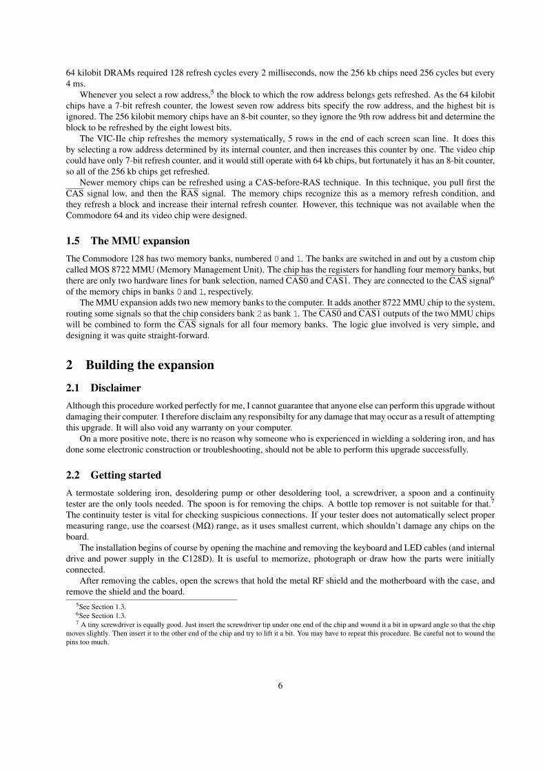
Figure 3: The schematics diagram of the PIA expansion. See text.
If you are going to expand your machine only to 256 kilobytes, skip the following subsection. If you aim to awhole megabyte, expand your computer first to 512 kilobytes, and then make the MMU expansion.
2.3 Expanding to 512 kilobytesThe PIA expansion consists of one daughter board, which contains most of the added logic, one piggy-backed chip,and a spaghetti of wires.
In Figure 3, there is a schematics diagram of the daughter board for the PIA expansion. There are some signalsthat you must wire to the mother board. You can take the I/O2 and A7 signals from the cartridge port, or from somethrough-put location near the daughter board. The I/O2 signal should be on the pin 7 of the chip U3 (74LS138). TheA7 can be also taken from the MMU’s (U7, MOS 8722) pin 23, in which case the address range of the PIA willbe limited to $DFC0–$DFFF instead of $DF80–$DFFF, or from the 8502’s pin 14. It is also on the multiplexor U14(74LS257A), in pin 3.
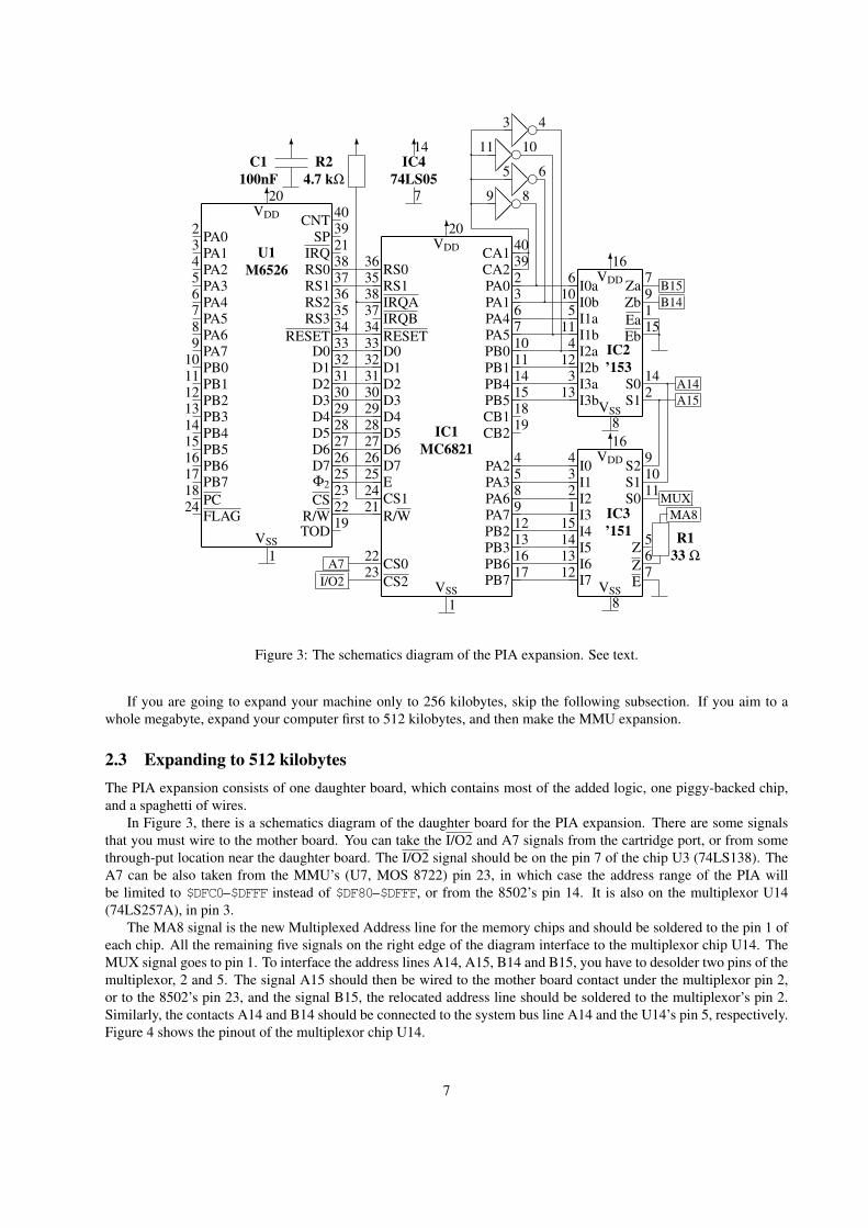
The MA8 signal is the new Multiplexed Address line for the memory chips and should be soldered to the pin 1 ofeach chip. All the remaining five signals on the right edge of the diagram interface to the multiplexor chip U14. TheMUX signal goes to pin 1. To interface the address lines A14, A15, B14 and B15, you have to desolder two pins of themultiplexor, 2 and 5. The signal A15 should then be wired to the mother board contact under the multiplexor pin 2,or to the 8502’s pin 23, and the signal B15, the relocated address line should be soldered to the multiplexor’s pin 2.Similarly, the contacts A14 and B14 should be connected to the system bus line A14 and the U14’s pin 5, respectively.Figure 4 shows the pinout of the multiplexor chip U14.
7
U14 74LS257Aª`
1 162 153 144 135 126 117 108 9
MUX VDD
TA15 AECA7 TA12
VMA7 A4TA14 VMA4
A6 TA13VMA6 A5
VSS VMA5
Figure 4: Pin-out for the multiplexer chip U14
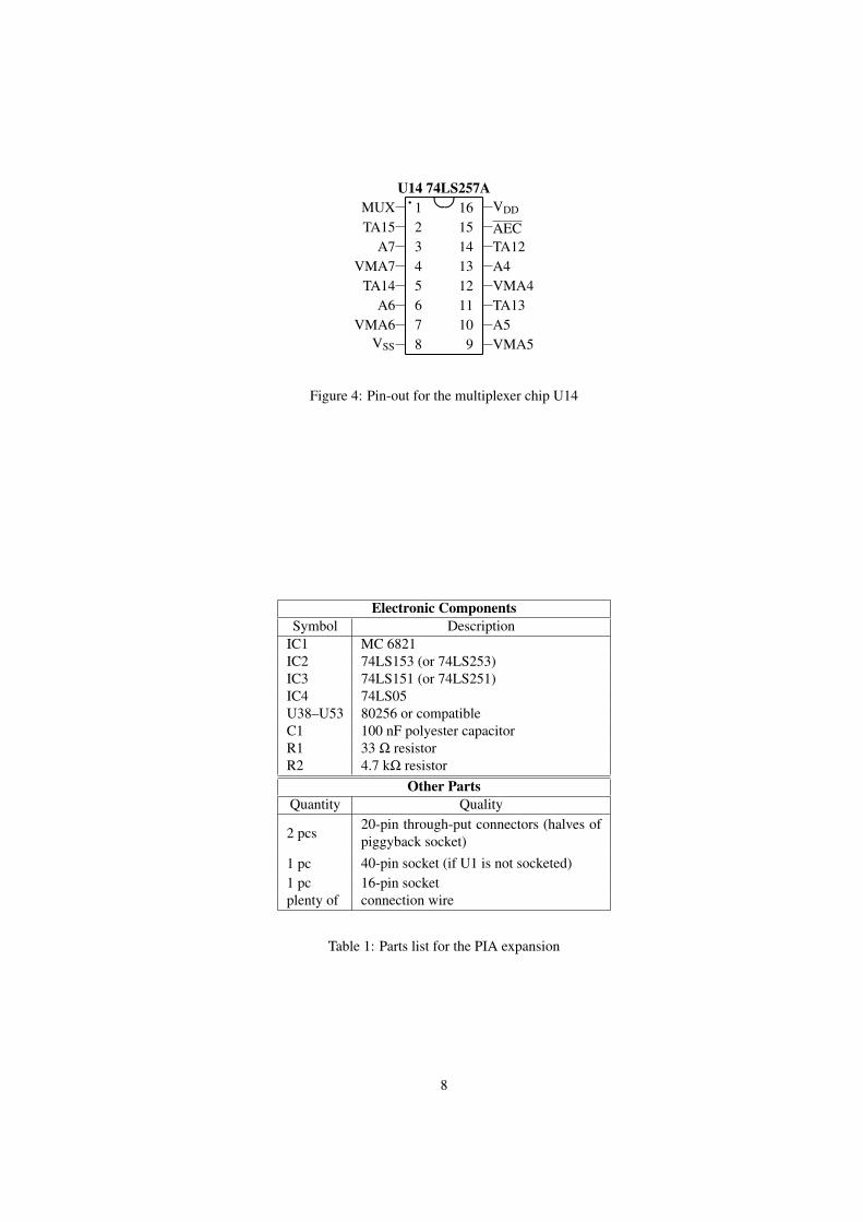
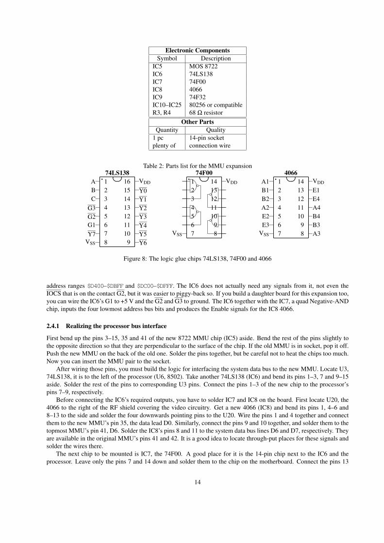
Electronic ComponentsSymbol Description
IC1 MC 6821IC2 74LS153 (or 74LS253)IC3 74LS151 (or 74LS251)IC4 74LS05U38–U53 80256 or compatibleC1 100 nF polyester capacitorR1 33 Ω resistorR2 4.7 kΩ resistor
Other PartsQuantity Quality
2 pcs20-pin through-put connectors (halves ofpiggyback socket)
1 pc 40-pin socket (if U1 is not socketed)1 pc 16-pin socketplenty of connection wire
Table 1: Parts list for the PIA expansion
8
MOS 6526 CIA MC 6821 PIAª ª` `
1 12 23 34 45 56 67 78 89 910 1011 1112 1213 1314 1415 1516 1617 1718 1819 1920 2021 21
22 2223 2324 2425 2526 2627 2728 2829 2930 3031 3132 3233 3334 3435 3536 3637 3738 3839 3940 40VSS VSS
PA0 PA0PA1 PA1PA2 PA2PA3 PA3PA4 PA4PA5 PA5PA6 PA6PA7 PA7PB0 PB0PB1 PB1PB2 PB2PB3 PB3PB4 PB4PB5 PB5PB6 PB6PB7 PB7
PCTOD
CB1CB2
VDD VDDIRQR/WCSFLAG
Φ2
R/WCS0CS2CS1E
D7 D7D6 D6D5 D5D4 D4D3 D3D2 D2D1 D1D0 D0RESET RESETRS3RS2RS1RS0SPCNT
RS1RS0IRQBIRQACA2CA1
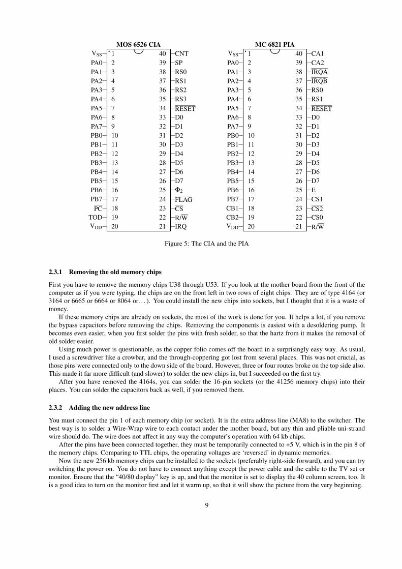
Figure 5: The CIA and the PIA
2.3.1 Removing the old memory chips
First you have to remove the memory chips U38 through U53. If you look at the mother board from the front of thecomputer as if you were typing, the chips are on the front left in two rows of eight chips. They are of type 4164 (or3164 or 6665 or 6664 or 8064 or. . . ). You could install the new chips into sockets, but I thought that it is a waste ofmoney.
If these memory chips are already on sockets, the most of the work is done for you. It helps a lot, if you removethe bypass capacitors before removing the chips. Removing the components is easiest with a desoldering pump. Itbecomes even easier, when you first solder the pins with fresh solder, so that the hartz from it makes the removal ofold solder easier.
Using much power is questionable, as the copper folio comes off the board in a surprisingly easy way. As usual,I used a screwdriver like a crowbar, and the through-coppering got lost from several places. This was not crucial, asthose pins were connected only to the down side of the board. However, three or four routes broke on the top side also.This made it far more difficult (and slower) to solder the new chips in, but I succeeded on the first try.
After you have removed the 4164s, you can solder the 16-pin sockets (or the 41256 memory chips) into theirplaces. You can solder the capacitors back as well, if you removed them.
2.3.2 Adding the new address line
You must connect the pin 1 of each memory chip (or socket). It is the extra address line (MA8) to the switcher. Thebest way is to solder a Wire-Wrap wire to each contact under the mother board, but any thin and pliable uni-strandwire should do. The wire does not affect in any way the computer’s operation with 64 kb chips.
After the pins have been connected together, they must be temporarily connected to +5 V, which is in the pin 8 ofthe memory chips. Comparing to TTL chips, the operating voltages are ‘reversed’ in dynamic memories.
Now the new 256 kb memory chips can be installed to the sockets (preferably right-side forward), and you can tryswitching the power on. You do not have to connect anything except the power cable and the cable to the TV set ormonitor. Ensure that the “40/80 display” key is up, and that the monitor is set to display the 40 column screen, too. Itis a good idea to turn on the monitor first and let it warm up, so that it will show the picture from the very beginning.
9
If the screen shows up normally, you may not (yet) have made any mistakes. If it does not show up at all, youhave to find possible cut-outs and shorts. Multi-colored ‘@’s show up usually because of too small bypass capacitors.Another cause is that the pin 1 is not connected to +5 V. In this case the screen may come up normally, but a little dis-turbance in the operating voltage locks the computer up. Now the computer should operate exactly like an unexpandedC128, so any previously working program should work with it.
2.3.3 Prepare for the final step
Next you remove U14 (74LS257, to the right of the memory chips) and U1 (MOS 6526, near the keyboard connector).Either or both of these chips may already be on sockets, and you must remove the rest. Reinsert the chips and check ifthe machine boots up.
If the computer does not work on first try, remember to disconnect any cables from it before trying to fix theproblem. The soldering iron may occasionally give little electric pulses to the computer, and this might burn someexpensive chips, especially if the computer is hooked to a wall outlet or a television set.
When you have completed the preparations, you can start building the control logic. You could build the wholeexpansion by piggy-backing chips, that is, by soldering new chips on the top of old ones, bending some feet to the side,and connecting messy wires all over your computer. However, the best way is to put most of the chips on a daughterboard. I used only a small daughter board, and piggy-backed five or six chips, but you can be wiser and put all newchips on the daughter board.
My daughter board interfaces the heart of the expansion, MC 6821 PIA, to the bus of the computer through the pinsof U1, the MOS 6526 CIA near the keyboard connector. The CIA is raised on the board, and its pins are lenghtenedwith two through-put socket halves, so that they can reach the socket on the mother board. I built the daughter boardon an uncoppered prototype board, a plastic board with holes punched in it at a 1/10 inch grid.
The room reserved for the mother board in the C128 and C128D is very shallow, about one third of the height inthe C64. In addition to that, the front edge of the mother board must be even shallower, as the metal shield has an anglein it. Due to this, you cannot use any sockets in the CIA daughter board, and you have to choose the chip layout verycarefully. My daughter board has the PIA chip on the left side of the CIA. To leave room for the MMU expansion, Icould put only two chips (IC2 and IC3) horizontally next to the notched end of the PIA (IC1) and CIA (U1). I placedthe inverter (IC4) with the 100 nF bypass capacitor near the other end of the PIA chip.
A far better way is to interface the daughter board to the socket of U7 (MOS 8722 MMU). There are not so terriblespace limitations, the RF shield is higher near the rear edge of the machine than on the front edge. In addition to that,the keyboard cable of the flat C128 is not so likely to damage that daughter board than the CIA board, which would benext to the keyboard connector. The MMU daughter board would allow you to make an easily removable expansion,as no chips would be piggy-backed. You could even make an option for installing a second MOS 65818 SID (SoundInterface Device) on the board to get stereo sound. However, this board should be etched, as the PIA and MMU pinlayouts differ very much from each other. See Figure 7 for pinouts for the MMU. Pinouts for the PIA and CIA arepresented in Figure 5.
Building the CIA daughter board was a real pain. I had to solder the CIA directly to the piggy-back socket pins,and I even bent the CIA pin ends aside, so that I could make it about 1 mm shallower. I put the CIA pins and thethrough-put socket halves to the same holes and started soldering. To keep the socket halves parallel, I put one halfagainst the outside of the CIA pins, and the other half against the inside. It was very easy to solder the half whosecontacts were outside the pins, but the other half was a real pain. It could be done by heating a CIA pin, insertingsome solder from the side, and hoping that it connects the piggy-back socket pin. I had to solder those pins four orfive times.
After raising the CIA on the daughter board, it is a very good idea to insert the board to the socket and check if themachine boots up. If some of the right side pins (21–40) are loose, the machine can jump to ML monitor due to anunexpected interrupt, or it can misread the keyboard. In the C64 mode, it will probably jam.
The next step is to add the PIA on the board. The contacts from the CIA except the operating voltages may bedifficult to route. I solved the problem by putting the wires through the very small holes that were left between thebiggy-back socket halves and the down surface of the daughter board. It was very painful, but the design is verycompact. After soldering all CIA contacts to the PIA, I wired the inverter and the rest of the chips. To increasereliability, I used thin multi-strand wire, as uni-strand wire gets easily loose when you push it.
88580 for the 9 volt version
10
Since I had finished the daughter board, I bent up the pins 2 and 5 of the U14 multiplexer chip, and connected itspins 1–3 and 5 to the daughter board with wires. First I inserted the wires for A14 and A15 directly to the chip socket,but as it turned out to be unreliable, I located a through-put place for each line, and soldered the wires there instead.
When you have wired the multiplexer U14, remove the jumper wire between MA8 and +5 V and connect thataddress line to the daughter board. Then connect the PIA’s CS line to I/O2, which is in U3’s pin 7 (or one of thethrough-put places along the trace’s path to the cartridge port), and insert the daughter board to the socket. Switch thepower on and pray that your dear computer works.
If you get only crap consisting of @’s or some randomly changing graphics on the 40 column screen, check thatall CIA pins have a good contact to the piggy-back socket, and that the wires from U14 and its socket are firmlyconnected. If it doesn’t help, you have to check all daughter board connections with the continuity tester. Don’t panic,you can ensure that the computer works by connecting the MA8 line back to +5 V, by bending the U14 lines backdown, and by inserting a spare CIA chip to the CIA socket.
2.3.4 Testing
After you have installed the boards to your machine, it is time to test the connections. You can connect LED, keyboardand probably disk drive in addition to the power cable and the TV cable, but do not fasten the mounting screws yet. Ifthe 40 column screen shows up and if the machine seems to operate, input the following test program:
10 PB=5728220 POKE PB,255:POKE PB+1,4:POKE PB,25530 PRINT"PRESS A KEY AFTER THIS HAS DISAPPEARED":
FOR I=0 TO 3000:NEXT40 POKE PB,14:WAIT 198,15:GET A$:POKE PB,255
On the line 10 a variable PB is set up. It is the address of the peripheral and data direction registers for the 6821port B, and the block selection register of the segments 2 and 3 and the VIC-IIe.
The line 20 contains initialization of PIA: the lines PB0–PB7 are set outputs, the data direction register is switchedto data register with ‘POKE PB+1,4’, and the PB lines are set high.
On the line 40 VIC-IIe is given block 0 ($00000–$0FFFF) of the default bank (0), and then the program waits fora keypress and restores the block F ($30000–$3FFFF).
If this test program works as expected, the screen will be filled with ‘@’s and other random characters.At this point, you may want to switch to the C64 mode and to run the TEST program, which is among the distribu-
tion files.9 Also, you can try the PIAGLOBE.128 program to test almost all of the 512 kB or 1024 kB memory.The PIAGLOBE.128 program is based on Georg Schwarz’s globe spinner GLOBE.64 that uses two graphics screens.
He has made a slightly faster version for the C128, utilizing the 2 MHz mode in the screen border. But compared to it,PIAGLOBE.128 is from other planet. Depending on the amount of memory available, it calculates 112 or 56 picturesof the globe and then uses them in a continuous animation. One revolution will last approximately 2.23 seconds onPAL systems and 1.87 seconds on NTSC. As the calculation phase lasts more than a minute, the program changes thescreen color between each picture.
On NTSC systems, the edge of the globe might not display correctly. The edge is rounded with 24 sprites, whichare moved around by a raster interrupt routine, starting from $4801. I did not bother to think about the timings, sinceI had enough troubles with relocating the program and the tables, and in trying to get all that graphics data to fit in thememory. In the distant future I might make a better looking version of the globe spinner, who knows. There is over 80kilobytes of unused memory when running the program on a C1028.
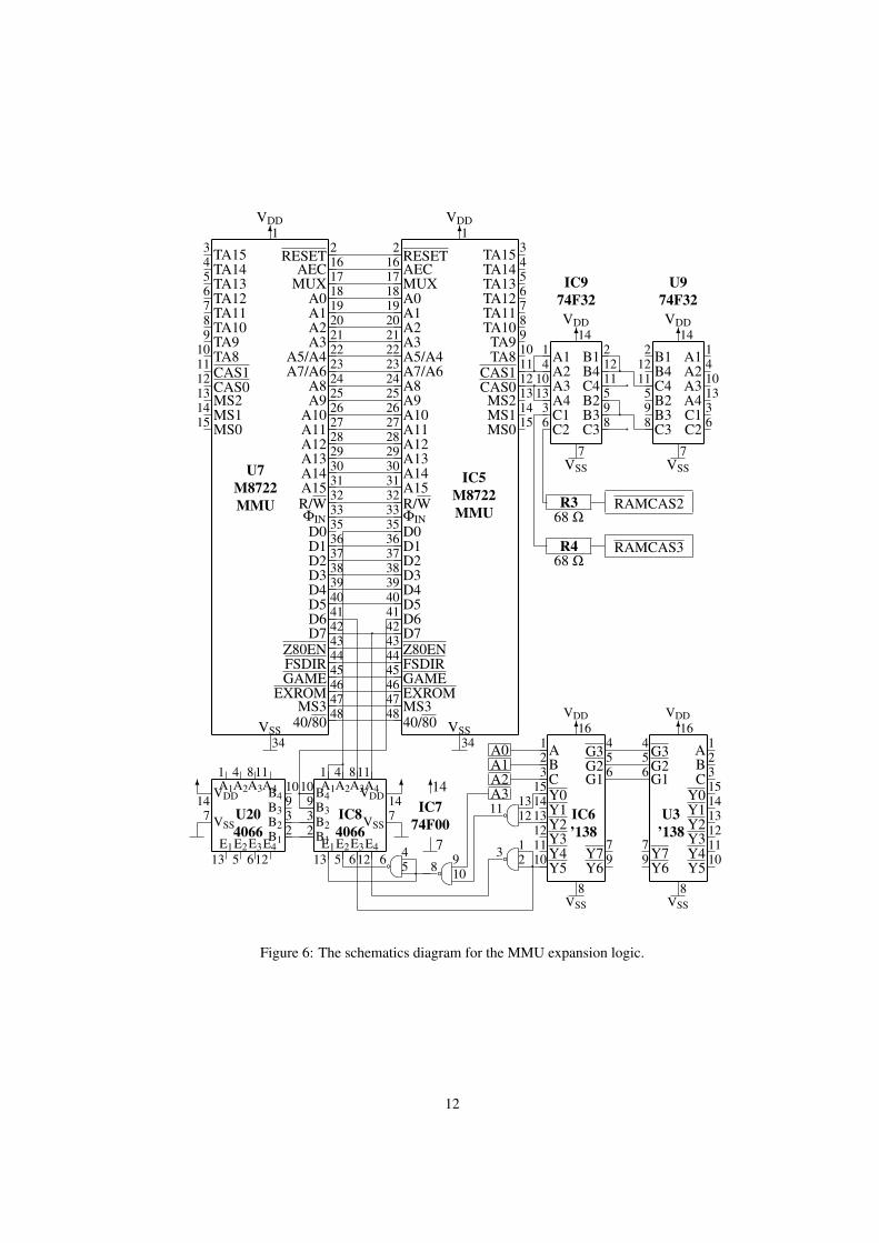
2.4 Expanding to 256 or 1024 kilobytesThis MMU expansion is far easier to understand than the PIA expansion, and maybe faster to build, too. You have tosolder the new MMU and a couple of logic chips on top of some chips laying on the mother board, or to install themon a daughter board. I chose the piggy-backing method.
The biggest problem with this expansion is that the MOS 8722 MMU is a custom chip from Commodore, andit is only used in the Commodore 128, which has not been manufactured for ages. If you do not happen to have a
9See Section 5.1.
11
U7M8722MMU
IC5M8722MMU
IC974F32
U974F32
U204066
IC84066
IC774F00
IC6’138
U3’138
63 TA154 TA145 TA136 TA127 TA118 TA109 TA910 TA811
CAS112CAS013 MS214 MS115 MS0
34VSS
4840/80
47MS3
46EXROM
45GAME
44FSDIR
43Z80EN
42D741D6
40D5
39D4
38D3
37D2
36D1
35D0
33ΦIN
32R/W
31A15
30A14
29A13
28A12
27A11
26A10
25A9
24A8
23A7/A6
22A5/A4
21A3
20A2
19A1
18A0
17MUX16AEC
2RESET
1VDD
63TA15 4TA14 5TA13 6TA12 7TA11 8TA10 9TA9 10TA8 11
CAS1 12CAS0 13MS2 14MS1 15MS0
34VSS
4840/80
47 MS3
46EXROM
45GAME
44FSDIR
43Z80EN
42 D741 D6
40 D5
39 D4
38 D3
37 D2
36 D1
35 D0
33 ΦIN
32R/W
31 A15
30 A14
29 A13
28 A12
27 A11
26 A10
25 A9
24 A8
23 A7/A6
22 A5/A4
21 A3
20 A2
19 A1
18 A0
17 MUX16 AEC
2RESET
1VDD
61 A14 A210 A313 A43 C16 C2
7VSS
8C3
9B3
5B2
11C4
12B4
2B1
14VDD
62 B112 B411 C45 B29 B38 C3
7VSS
6C2
3C1
13A4
10A3
4A2
1A1
14VDD
6
13E1
5E2
6E312
E4
1A1
4A2
8A3
11A4
2B1
3B2
9B3
10B4
7 VSS
14VDD 6
13E1
5E2
6E312
E4
1A1
4A2
8A3
11A4
2 B1
3 B2
9 B3
10 B4
7VSS
14VDD 614
7
a
a
®®2
13
121311
a a®
®
546
1098
61 A2 B3 C15
Y014Y113Y212Y311Y410Y5
8VSS
9Y6
7Y7
6G1
5G2
4G3
16VDD
61A 2B 3C 15
Y0 14Y1 13Y2 12Y3 11Y4 10Y5
8VSS
9Y6
7Y7
6 G1
5G2
4G3
16VDD
68 Ω
68 ΩR3
R4
``
`
``
`
RAMCAS2
RAMCAS3
`
`
`
A0A1A2A3
``
Figure 6: The schematics diagram for the MMU expansion logic.
12
wreck C128 lying around, you can try ordering the chip from Jameco Electronics. The chip shouldn’t cost more than10 USD. You can reach them at:
Orders (phone): 1-800-831-4242Orders (fax): 1-800-237-6948
Fax (overseas): +1-415-592-2503Mail: Jameco Electronics
1355 Shoreway RoadBelmont, CA 94002U.S.A.
MOS 8722 MMUª`
123456789101112131415161718192021222324 25
2627282930313233343536373839404142434445464748VDD
RESETTA15TA14TA13TA12TA11TA10
TA9TA8
CAS1CAS0
MS2MS1MS0AEC
MUXA0A1A2A3
A5/A4A7/A6
A8 A9A10A11A12A13A14A15R/W
ΦIN
VSS
D0D1D2D3D4D5D6D7Z80ENFSDIRGAMEEXROMMS340/80
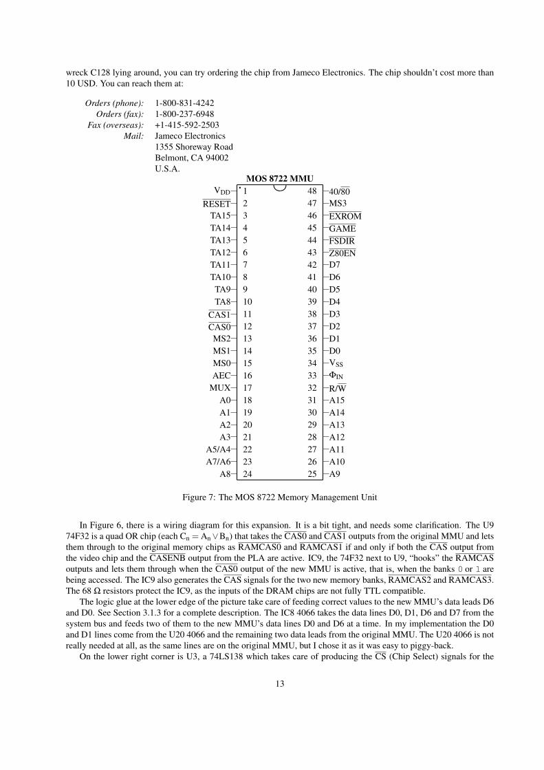
Figure 7: The MOS 8722 Memory Management Unit
In Figure 6, there is a wiring diagram for this expansion. It is a bit tight, and needs some clarification. The U974F32 is a quad OR chip (each Cn = An∨Bn) that takes the CAS0 and CAS1 outputs from the original MMU and letsthem through to the original memory chips as RAMCAS0 and RAMCAS1 if and only if both the CAS output fromthe video chip and the CASENB output from the PLA are active. IC9, the 74F32 next to U9, “hooks” the RAMCASoutputs and lets them through when the CAS0 output of the new MMU is active, that is, when the banks 0 or 1 arebeing accessed. The IC9 also generates the CAS signals for the two new memory banks, RAMCAS2 and RAMCAS3.The 68 Ω resistors protect the IC9, as the inputs of the DRAM chips are not fully TTL compatible.
The logic glue at the lower edge of the picture take care of feeding correct values to the new MMU’s data leads D6and D0. See Section 3.1.3 for a complete description. The IC8 4066 takes the data lines D0, D1, D6 and D7 from thesystem bus and feeds two of them to the new MMU’s data lines D0 and D6 at a time. In my implementation the D0and D1 lines come from the U20 4066 and the remaining two data leads from the original MMU. The U20 4066 is notreally needed at all, as the same lines are on the original MMU, but I chose it as it was easy to piggy-back.
On the lower right corner is U3, a 74LS138 which takes care of producing the CS (Chip Select) signals for the
13
Electronic ComponentsSymbol Description
IC5 MOS 8722IC6 74LS138IC7 74F00IC8 4066IC9 74F32IC10–IC25 80256 or compatibleR3, R4 68 Ω resistor
Other PartsQuantity Quality
1 pc 14-pin socketplenty of connection wire
Table 2: Parts list for the MMU expansion74LS138 74F00 4066
ª ª ª` ` `
8 9101112131415161 1 1
2 2 23 3 34 4 45 5 56 6 67 7 78 8
9 910 1011 1112 1213 1314 14A
BC
G3G2G1Y7
VSS Y6Y5Y4Y3Y2Y1Y0
VDD VDD VDD
VSS VSS
b
b
³´
³´
b
b
¶µ
¶µ
A1B1B2A2E2E3
A3B3B4A4E4E1
Figure 8: The logic glue chips 74LS138, 74F00 and 4066
address ranges $D400–$DBFF and $DC00–$DFFF. The IC6 does not actually need any signals from it, not even theIOCS that is on the contact G2, but it was easier to piggy-back so. If you build a daughter board for this expansion too,you can wire the IC6’s G1 to +5 V and the G2 and G3 to ground. The IC6 together with the IC7, a quad Negative-ANDchip, inputs the four lowmost address bus bits and produces the Enable signals for the IC8 4066.
2.4.1 Realizing the processor bus interface
First bend up the pins 3–15, 35 and 41 of the new 8722 MMU chip (IC5) aside. Bend the rest of the pins slightly tothe opposite direction so that they are perpendicular to the surface of the chip. If the old MMU is in socket, pop it off.Push the new MMU on the back of the old one. Solder the pins together, but be careful not to heat the chips too much.Now you can insert the MMU pair to the socket.
After wiring those pins, you must build the logic for interfacing the system data bus to the new MMU. Locate U3,74LS138, it is to the left of the processor (U6, 8502). Take another 74LS138 (IC6) and bend its pins 1–3, 7 and 9–15aside. Solder the rest of the pins to corresponding U3 pins. Connect the pins 1–3 of the new chip to the processor’spins 7–9, respectively.
Before connecting the IC6’s required outputs, you have to solder IC7 and IC8 on the board. First locate U20, the4066 to the right of the RF shield covering the video circuitry. Get a new 4066 (IC8) and bend its pins 1, 4–6 and8–13 to the side and solder the four downwards pointing pins to the U20. Wire the pins 1 and 4 together and connectthem to the new MMU’s pin 35, the data lead D0. Similarly, connect the pins 9 and 10 together, and solder them to thetopmost MMU’s pin 41, D6. Solder the IC8’s pins 8 and 11 to the system data bus lines D6 and D7, respectively. Theyare available in the original MMU’s pins 41 and 42. It is a good idea to locate through-put places for these signals andsolder the wires there.
The next chip to be mounted is IC7, the 74F00. A good place for it is the 14-pin chip next to the IC6 and theprocessor. Leave only the pins 7 and 14 down and solder them to the chip on the motherboard. Connect the pins 13
14
and 12 from the 74F00 to the IC6’s pins 15 and 13, and connect the 74F00’s pins 11 and 10 together. Then solder thepin 9 to the 8502’s pin 10, A3. Solder the IC7’s pin 8 to its own pins 4 and 5, and connect it also to the IC8 4066’spin 13. Connect the IC7’s pin 6 to the IC8’s pin 5. Lead the 74LS138’s pin 10 to the 4066’s pin 6 and to the 74F00’spins 1 and 2. Lead the 74F00’s pin 3 to the 4066’s pin 12.
After all these piggy-backings, it is wise to check if the computer powers up any more. If not, check the solderings.When I built this second version of the MMU expansion, I swapped the 4066 pins 9 and 10 by mistake, which resultedin a miserably black screen each time I desperately tried to power the computer up.
2.4.2 Adding the new memory banking signals
If the first stage succeeded, you can build the new logic for deriving the CAS signals for the two new RAM banks.Locate U9 (74F32) and lift it on a socket, if it was directly soldered to the system board. If the computer works afterthis operation, you can continue with the piggy-backing. Take a new 74F32 (IC9) and bend its all pins except 7, 9, 12and 14 to the side. Bend the pins 8 and 11 of the old 74F32 up, so that they can be connected to the IC9’s pins 9 and12, respectively. Connect the pins 7 and 14, too. Solder a short length of stiff uni-strand wire to the new 74F32’s pins8 and 11, in order that these pins reach the socket on the motherboard. Connect the pin 12 of the new MMU to theIC9’s pins 13 and 10.
Now the computer should work just as earlier, except that when you try to access the banks 2 or 3, the processorwill read randomly changing garbage. You can verify this by moving the cursor to the top left-hand corner of thescreen and typing “M 20400” or “M 30400” in the machine language monitor a couple of times.
To generate the signals RAMCAS2 and RAMCAS3, connect the topmost MMU’s pin 11 to the IC9’s pins 1 and 4,and solder the new 74F00’s pins 2 and 12 as well as the pins 5 and 9 together. Then mount R3 and R4, the 68 Ω resistorsto the new 74F00’s pins 6 and 3. On their free ends will be the RAMCAS2 and RAMCAS3 signals, respectively.
2.4.3 Soldering the memory chips
After ensuring that the computer works, you can prepare for the final step. Take the sixteen memory chips (4164’s orsimilar if you are aiming to the 256 kB memory expansion; 41256’s or similar for the 1024 kB expansion) and bendtheir pins 15 (CAS) up. Solder the remaining pins on top of the sixteen memory chips on the motherboard. Thencombine the CAS signals of the eight new memory chips at the front edge of the system board and connect them to R3or R4. Similarly, connect the pins 15 of the remaining memory chips and wire them to the remaining 68 Ω resistor.
Power the computer up again and pray until it works. If you can access the banks 2 and 3 as expected, congratula-tions! When re-assembling the chassis, be very careful with the RF shield. Especially measure that the CAS signalsfor the new memory banks have no contact with the shield.
3 Using the expansion
3.1 The operation of the block switcherThere are four new micro chips in the PIA expansion. The most important of them is the PIA chip MC 6821, whichholds the values of the block selections. The PIA has two 8-bit ports set up in the addresses 57280 and 57282. Theupper and lower four bits (nybbles) of each port determine which 16 kB block is mapped to each 16 kB segment ofthe processor’s address space. IC2 and IC3 participate in forming the memory block control signals.
There is a chip equivalent to the PIA even in Commodore’s own 6500 series, but it is not suitable for this con-nection, as it is not TTL compatible. The 6821 from Motorola 6800 series, which contains also processors remindingthose in the CSG10 6500 and 8500 series, is bus compatible and suitable for this purpose.
Commodore 128 asserts the 16 bit addresses to the original 64 kb chips in two parts. First it asserts the lower eightbits, then the higher eight. The 256 kb chips require two additional address bits, so the chips are given nine bits at atime. Due to this address multiplexing, the block selection bits cannot be directly input to the memory chips, but theymust be lead through the multiplexer circuitry of IC2, IC3 and U14.
IC4 contributes to the operation during power-up. It ensures that the C128 gets reasonable memory blocks to itsdifferent segments. In the beginning the segments are filled with four upmost memory blocks.
10Commodore Semiconductor Group; former Mostek or MOS Technologies
15
3.1.1 PIA’s location in address space
The PIA’s data bus and E, RESET and R/W signals have been connected directly to the 6526 chip. Similarly are theRS0 and the RS1, which select a PIA register, connected to A0 and A1.
The I/O block decoder (U3) tells us when the second I/O block is selected. This block resides in the area $DF00–$DFFF. The signal I/O2 is connected to the PIA’s chip selection pin CS, and it forms most of its addressing. Theaddress line A7 limit PIA’s area in I/O2 to $DF80–$DFFF, because it will be tied to the CS pin.
3.1.2 Block selection
As the address space has been divided to four segments of 16 kB, the A14 and A15 cannot be lead directly to thememory chips, but they participate in the block selection. These two address bits determine which of the four blocksis in use. For each segment, the PIA ports tell which memory block to map. Original A14 and A15 are connected toIC2 and IC3, which select the right output lines of PIA. For each 16 kB segment there are 4 output lines which formthe block address for the segment.
IC2 selects two lowest bits of the block address and feeds them to the address multiplexer chip U14 as B14 andB15. They are practically equivalent to the A14 and A15 signals. After the address bits A0–A7 have been assertedduring the first addressing cycle, IC2 asserts B14 and B15 during the second (CAS) cycle.
The 256 kb memory chips still need two extra address bits. The expansion must multiplex them with IC3, whichis a ‘one-of-eight’ multiplexer. Its eight inputs are tied to the two upmost bits of the four block addresses. A14 andA15 are connected to the IC3, but it needs yet another control signal to handle all eight input bits. This signal is MUX,which controls multiplexing other address bits (MA0–MA7) as well.
While the MUX signal is low and the memory chips are fed the lowest bits (A0–A7) of the address, the IC3 selectsthe third bit of the block address determined by A14 and A15. This bit is called address bit A16, and it is asserted tothe ‘extra’ address line MA8 simultaneously with the lowmost bits. When MUX is high, the upper address bits arefed, and IC3 selects the fourth bit of the block address determined by A14 and A15. It corresponds to the address bitA17 and is fed through the same MA8 with all the other upmost bits.
When the video chip accesses the bus, the address and data lines from the processors are in high-impedance state,driven to logical ‘1’ level with very weak current, so that the video chip can change their state easily. As the addresslines A14 and A15 (or actually TA14 and TA15 in the C128) are not connected to the VIC-IIe, they remain as logical‘1’ whenever the video chip has the bus. Thus, the switcher logic ‘thinks’ that the address range $C000–$FFFF is beingaddressed, and it selects the block for that segment also for the VIC-IIe.
The resistor on the MA8 line protects the IC3, because the inputs of dynamic memories are not fully TTL compat-ible.
3.1.3 Interfacing the second MMU
The new MMU must be fooled so that it mistakes the memory bank 2 for bank 1. This can be done by connectingits data bit D6 to the system data line D7 whenever the RAM Configuration Register (location $D50611) or any ofthe Configuration Registers ($D500–$D504 and $FF00–$FF0412) are being accessed. In addition to this, the pagerelocation registers must be taken into consideration, or you could relocate the processor pages 0 and 1 only to banks0 or 3. For this reason, the MMU data line D1 must be connected to system data line D0 when the locations $D508 or$D50A are being accessed. There is a commercial 256 kB or 512 kB expansion for the C128 that does not take care ofthis.
Actually the logic rules can be relaxed, and the MMU pin D6 can be connected to system D7 for most time. Theonly register that needs the D6 line to be connected to system D6 is the Mode Configuration Register ($D505).13
Connecting the D1 and D6 pins is performed by three chips: 74LS138, 74F00 and 4066. Consult Figure 8 for theirpinouts. The 74LS138 inputs a 3-digit binary number through its A, B and C pins and converts it to an octal digit byactivating one of its eight output lines Yn, provided that the chip has been selected with the G inputs. The 74F00 is aquad Negative-AND chip, and the 4066 is a quad analog switch. It connects its An and Bn contacts together wheneverthe respective En pin is in the logical ‘1’ state. The IC6 74LS138 and the IC7 74F00 generate the E signals for the IC84066 from the system address lines A0–A3.
11See Table 10.12See Table 8.13See Table 9.
16
3.1.4 Startup settings for the PIA expansion
In order to enable the operation of the machine, each of the four segments must be mapped to a unique memory block.The Commodore 64 Kernal tests the lowmost continuous area of writeable memory and would hang up, if the sameblock was mapped to both $0000 and to $4000, for instance. Modifying the startup routines would cure this problem,but in that case the Kernal ROM chip should be changed. Also the C128 Kernal would need some patching, if youdon’t want to run any initializer program every time you start the computer up.
The bootup state can be achieved otherwise. The RESET signal sets all the PIA port lines to inputs. As input aline has an impedance of several megaohms. A TTL chip reads such a signal as a logical ‘1’. IC4 can force four blockselection pins (PA0, PA1, PA5 and PB0) low, so that the memory segments of C64 point to the four upmost memoryblocks in ascending order. The port A contains the bits 1101 1100 and the port B 1111 1110. As the IC4 has opencollector outputs, it doesn’t disturb the port’s operation when outputting high state. That is why the initializationroutines14 write the value 52 to the address 57281, which forces the IC4 outputs high by lowering the CA2 line.
3.2 Segmented memoryThe address space of Commodore 128 consists of four 16 kB segments which are at the address ranges $0000–$3FFF,$4000–$7FFF, $8000–$BFFF and $C000–$FFFF. A PIA expanded C128 uses the topmost four 16 kB blocks of eachbank after startup. It considers them as its whole world and does not know anything of the other memory blocks.Figure 1 describes the situation. A total of twelve memory blocks of each memory bank are left out of the C128’sworld.
With expanded memory we can cheat the C128 by writing a suitable number to a known address, in order to makeit consider the lowmost block as the second segment, for example. Then all operation that the C128 does at the secondsegment’s area alter in fact the lowmost block, although the computer has no idea of it. This is the idea behind thewhole PIA expansion circuit.
What is the benefit of it? The second segment (segment 1) is actually a good example of the function, because itresides in the middle of the RAM reserved for C64 BASIC programs. If we make a little C64 BASIC program thatholds an array exactly in the third segment, we can switch another memory block to that area while the program isrunning, and we have another 16 kilobytes to expand our table. In this manner all unused memory blocks (12× 16kilobytes) of the memory bank selected for the C64 mode (0 by default) can be taken in use, and the memory is ableto hold enormous arrays, which can be accessed simply by switching the memory block. See Example 4.1 for anexample of this technique.
Another and more useful way to exploit the extra blocks is to use them as a RAM disk. A RAM disk means thatyou can copy even a whole disk to these blocks and consider it as a new disk drive, from which you can load programand data at a very fast speed. For a RAM disk you need a smart program that redirects disk commands and executesthem on the expanded memory.15
3.3 Critical addresses for the PIA expansionThe critical addresses of the device are 57216–57343 ($DF80–$DFFF). There is the PIA chip to which you POKE thevalues to switch memory blocks. The PIA does not have 128 registers, as one might think. There are sixteen copiesof its 4 addresses in that memory area. For instance, the addresses 57216, 57284, 57288 and 57340 are equivalent toeach other.
57280 is a memory place whose lowmost four bits (bits 0–3, low nybble) determine, which of the sixteen memoryblocks is accessed through the lowmost segment (segment 0) of Commodore 128. The upper four bits (bits 4–7, highnybble) specify, which of the blocks show up at the second segment (segment 1). In a similar manner the low nybbleof the address 57282 determines which block resides at segment 2, and the high nybble tells the block addressed viathe upmost segment.
These addresses have even another function. They can act as data direction registers as well, i.e. tell if the port linesare inputs or outputs. However, this application uses only some of the PIA’s characteristics. For normal operation, allthe port lines should be set to outputs. The function of these addresses depend on the bit 2 of the next address. Forinstance, the function of 57280 is defined with the address 57281. If you POKE there a value with its third bit set, the
14See Section 3.4.15See Section 5.4.
17

values written to 57280 will go to the data direction register. Inputs have the corresponding data direction register bitsreset, and outputs have them set. See Tables 3–6 for a complete description of PIA registers.
18
3.4 Initializing the PIA expansionThe second MMU, if any, does not need any initialization. In contrary to that, the PIA does. Before using thatexpansion memory, you have to first initialize the PIA. Every time when a RESET is issued, the PIA registers changeto the default state.16 In the beginning of your program you will initialize the PIA registers so that the default blockdivision of memory remains:
pia .equ $DFC0
LDA pia+1 ; Select Peripheral RegistersORA #4STA pia+1TAXLDA pia+3ORA #4STA pia+3TAY
LDA #$FE ; Set the default memory block dataSTA pia+2LDA #$DCSTA pia
TXA ; Select Data Direction RegistersAND #$FBSTA pia+1TYAAND #$FBSTA pia+3
LDA #$FF ; Set the ports to outputSTA piaSTA pia+2
TXAAND #$C7ORA #$30 ; Set CA1 andSTA pia+1 ; select Peripheral RegistersSTY pia+3
16See Section 3.1.4.
19
You may want to use an array instead. That will save both space and processing time but lose generality. Someonemay have CB1 or CB2 in use,17 and changing all the command register bits causes side effects on these pins. Anyway,here is a BASIC example of using an initialization table:
10 PIA=5728020 FOR I=11 to 1 STEP -1:READ A:POKE PIA+I,A:NEXT30 DATA 4,254,4,220,0,255,0,255,4,254,52
Many Commodore 64 games do not like any extra hardware in the area $DE00–$DFFF, as it is used by many“freezer” cartridges and alike. If you need to use such software with the memory expansion, you can completelydisable the PIA from the address space until a system RESET occurs. To do this, change the last DATA value on theline 30 from 52 to 53. By the way, the PIA expansion can be easily enhanced to be the most powerful freezer cartridge.See Section 6.1 if you are interested in this.
3.5 Programming the PIA in machine languageThink it in hexadecimal numbers. There are sixteen memory blocks, numbered from 0 to F. The address $DFC0holds two hexadecimal digits. The less significant digit, the one at right, selects the memory block for the segment 0($0000–$3FFF), whereas the other digit is for segment 1. The other important PIA address, $DFC2, selects the blocksfor segments 2 and 3 with is low and high nybble, respectively.
For instance, if you want to switch block E ($38000–$3BFFF) to segment 1, initialize the PIA and execute thefollowing. Note that your program must run outside segment 1 ($4000–$7FFF), or otherwise the next instruction willbe fetched from the new block, thus probably crashing the processor.
pia .equ $DFC0
LDA pia ; Segments 0 and 1AND #$0F ; Preserve segment 0ORA #$E0 ; Select block E for segment 1STA pia
If you used our initialization routine before this, the memory areas $4000–$7FFF and $8000–$BFFF should nowmirror each other. This is an easy way to peek under ROMs and I/O with a simple C64 mode machine languagemonitor that does not play with the 8502’s I/O registers to switch ROMs and I/O temporarily out. Also, this techniquecan be used in the C128 machine language monitor to access the lowest 4 kB of other memory banks than 0.18
3.5.1 An exception: video memory
As the video chip’s address bus is only fourteen bits wide, it can access only sixteen kilobytes directly. The twoadditional lines needed to address 64 kB are provided by the second CIA. Its lines PA1 and PA0 are the inverse ofthe VIC-IIe’s address lines VA15 and VA14. The video RAM bank is selected with the two upmost bits of the MMUregister $D506,19 and it does not necessarily need to be equal with the processor bank.
The VIC-IIe needs another two address lines to see full 256 kB of the selected RAM bank. The PIA lines PB7 andPB6 (the uppest two bits of $DFC2) serve as VA17 and VA16. So, the VIC-IIe memory does not necessarily have tobe accessible to 8502, but there is a restriction: As the block selector for the upmost segment uses the same two lines,both the VIC block and the block for segment 3 cannot be chosen freely.
For instance, if you want the VIC to ‘see’ its RAM at $04000, the lines VA17–VA14 must be ‘0001’. You canselect only blocks 0–3 for segment 3 to fulfill this condition. Let’s assume that you want block 2 to be mapped there:
17See Section 6.18
The built-in monitor for the C128 mode ignores the bank address when reading from the addresses $0000–$03FF, and reads the data always frombank 0. You can work this around by mapping some other address range, like $C000–$FFFF, to the same block that the segment 0 uses. Then youcan read from, say, $0000 in bank 2, by issuing the command M 2C000.
19See Table 10.
20
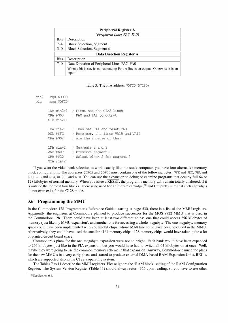
Peripheral Register A(Peripheral Lines PA7–PA0)
Bits Description7–4 Block Selection, Segment 13–0 Block Selection, Segment 0
Data Direction Register ABits Description7–0 Data Direction of Peripheral Lines PA7–PA0
When a bit is set, its corresponding Port A line is an output. Otherwise it is aninput.
Table 3: The PIA address $DFC0 (57280)
cia2 .equ $DD00pia .equ $DFC0
LDA cia2+1 ; First set the CIA2 linesORA #$03 ; PA0 and PA1 to output.STA cia2+1
LDA cia2 ; Then set PA1 and reset PA0.AND #$FC ; Remember, the lines VA15 and VA14ORA #$02 ; are the inverse of them.
LDA pia+2 ; Segments 2 and 3AND #$0F ; Preserve segment 2ORA #$20 ; Select block 2 for segment 3STA pia+2
If you want the video bank selection to work exactly like in a stock computer, you have four alternative memoryblock configurations. The addresses $DFC2 and $DFC0 must contain one of the following bytes: $FE and $DC, $BA and$98, $76 and $54, or $32 and $10. You can use the expansion to debug or examine programs that occupy full 64 or128 kilobytes of normal memory. When you issue a RESET, the program’s memory will remain totally unaltered, if itis outside the topmost four blocks. There is no need for a ‘freezer’ cartridge,20 and I’m pretty sure that such cartridgesdo not even exist for the C128 mode.
3.6 Programming the MMUIn the Commodore 128 Programmer’s Reference Guide, starting at page 530, there is a list of the MMU registers.Apparently, the engineers at Commodore planned to produce successors for the MOS 8722 MMU that is used inthe Commodore 128. There could have been at least two different chips: one that could access 256 kilobytes ofmemory (just like my MMU expansion), and another one for accessing a whole megabyte. The one megabyte memoryspace could have been implemented with 256 kilobit chips, whose MA8 line could have been produced in the MMU.Alternatively, they could have used the smaller 4164 memory chips. 128 memory chips would have taken quite a lotof printed circuit board space.
Commodore’s plans for the one megabyte expansion were not so bright. Each bank would have been expandedto 256 kilobytes, just like in the PIA expansion, but you would have had to switch all 64 kilobytes on at once. Well,maybe they were going to use the common memory scheme in that expansion. Anyway, Commodore canned the plansfor the new MMU’s in a very early phase and started to produce external DMA-based RAM Expansion Units, REU’s,which are supported also in the C128’s operating system.
The Tables 7 to 11 describe the MMU registers. Please ignore the ‘RAM block’ setting of the RAM ConfigurationRegister. The System Version Register (Table 11) should always return $20 upon reading, so you have to use other
20See Section 6.1.
21
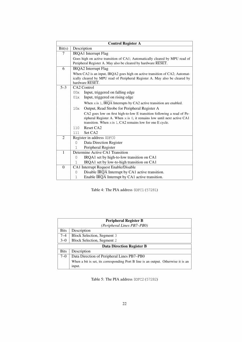
Control Register ABit(s) Description
7 IRQA1 Interrupt FlagGoes high on active transition of CA1; Automatically cleared by MPU read ofPeripheral Register A. May also be cleared by hardware RESET.
6 IRQA2 Interrupt FlagWhen CA2 is an input, IRQA2 goes high on active transition of CA2; Automat-ically cleared by MPU read of Peripheral Register A. May also be cleared byhardware RESET.
5–3 CA2 Control00x Input, triggered on falling edge01x Input, triggered on rising edge
When x is 1, IRQA Interrupts by CA2 active transition are enabled.10x Output, Read Strobe for Peripheral Register A
CA2 goes low on first high-to-low E transition following a read of Pe-ripheral Register A. When x is 0, it remains low until next active CA1transition. When x is 1, CA2 remains low for one E cycle.
110 Reset CA2111 Set CA2
2 Register in address $DFC00 Data Direction Register1 Peripheral Register
1 Determine Active CA1 Transition0 IRQA1 set by high-to-low transition on CA11 IRQA1 set by low-to-high transition on CA1
0 CA1 Interrupt Request Enable/Disable0 Disable IRQA Interrupt by CA1 active transition.1 Enable IRQA Interrupt by CA1 active transition.
Table 4: The PIA address $DFC1 (57281)
Peripheral Register B(Peripheral Lines PB7–PB0)
Bits Description7–4 Block Selection, Segment 33–0 Block Selection, Segment 2
Data Direction Register BBits Description7–0 Data Direction of Peripheral Lines PB7–PB0
When a bit is set, its corresponding Port B line is an output. Otherwise it is aninput.
Table 5: The PIA address $DFC2 (57282)
22
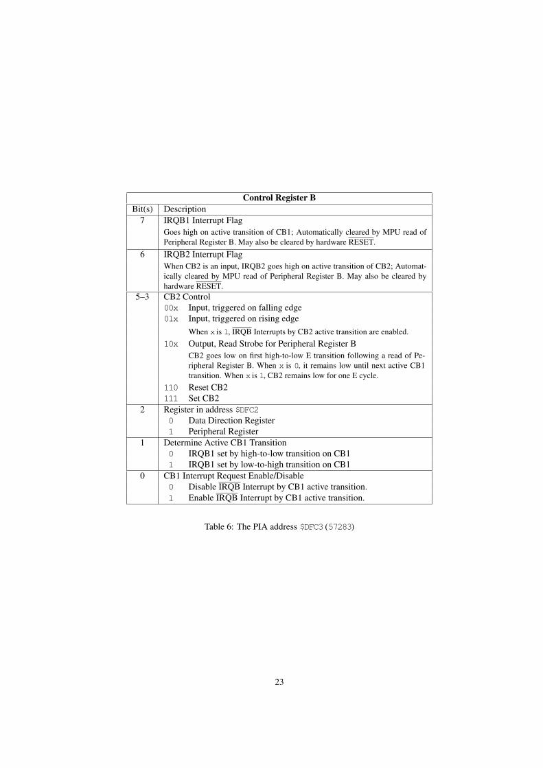
Control Register BBit(s) Description
7 IRQB1 Interrupt FlagGoes high on active transition of CB1; Automatically cleared by MPU read ofPeripheral Register B. May also be cleared by hardware RESET.
6 IRQB2 Interrupt FlagWhen CB2 is an input, IRQB2 goes high on active transition of CB2; Automat-ically cleared by MPU read of Peripheral Register B. May also be cleared byhardware RESET.
5–3 CB2 Control00x Input, triggered on falling edge01x Input, triggered on rising edge
When x is 1, IRQB Interrupts by CB2 active transition are enabled.10x Output, Read Strobe for Peripheral Register B
CB2 goes low on first high-to-low E transition following a read of Pe-ripheral Register B. When x is 0, it remains low until next active CB1transition. When x is 1, CB2 remains low for one E cycle.
110 Reset CB2111 Set CB2
2 Register in address $DFC20 Data Direction Register1 Peripheral Register
1 Determine Active CB1 Transition0 IRQB1 set by high-to-low transition on CB11 IRQB1 set by low-to-high transition on CB1
0 CB1 Interrupt Request Enable/Disable0 Disable IRQB Interrupt by CB1 active transition.1 Enable IRQB Interrupt by CB1 active transition.
Table 6: The PIA address $DFC3 (57283)
23
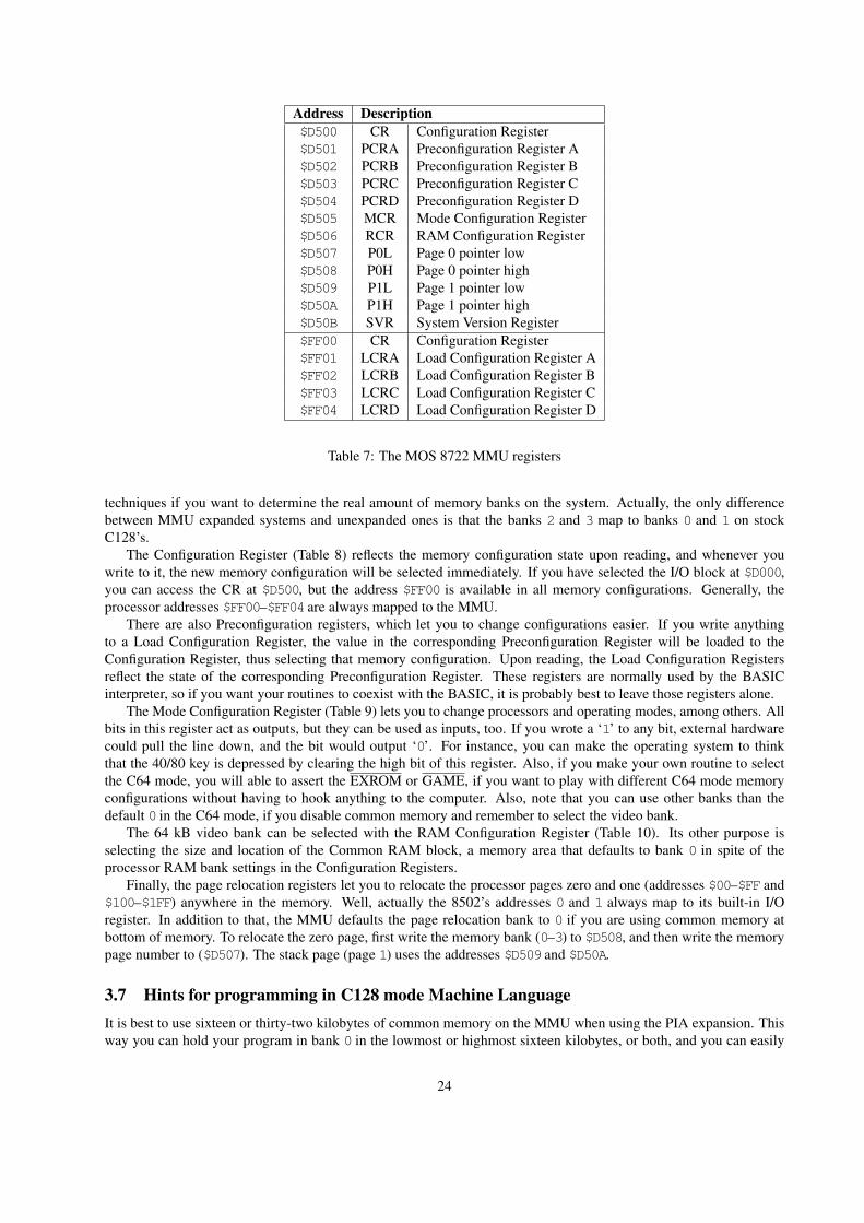
Address Description$D500 CR Configuration Register$D501 PCRA Preconfiguration Register A$D502 PCRB Preconfiguration Register B$D503 PCRC Preconfiguration Register C$D504 PCRD Preconfiguration Register D$D505 MCR Mode Configuration Register$D506 RCR RAM Configuration Register$D507 P0L Page 0 pointer low$D508 P0H Page 0 pointer high$D509 P1L Page 1 pointer low$D50A P1H Page 1 pointer high$D50B SVR System Version Register$FF00 CR Configuration Register$FF01 LCRA Load Configuration Register A$FF02 LCRB Load Configuration Register B$FF03 LCRC Load Configuration Register C$FF04 LCRD Load Configuration Register D
Table 7: The MOS 8722 MMU registers
techniques if you want to determine the real amount of memory banks on the system. Actually, the only differencebetween MMU expanded systems and unexpanded ones is that the banks 2 and 3 map to banks 0 and 1 on stockC128’s.
The Configuration Register (Table 8) reflects the memory configuration state upon reading, and whenever youwrite to it, the new memory configuration will be selected immediately. If you have selected the I/O block at $D000,you can access the CR at $D500, but the address $FF00 is available in all memory configurations. Generally, theprocessor addresses $FF00–$FF04 are always mapped to the MMU.
There are also Preconfiguration registers, which let you to change configurations easier. If you write anythingto a Load Configuration Register, the value in the corresponding Preconfiguration Register will be loaded to theConfiguration Register, thus selecting that memory configuration. Upon reading, the Load Configuration Registersreflect the state of the corresponding Preconfiguration Register. These registers are normally used by the BASICinterpreter, so if you want your routines to coexist with the BASIC, it is probably best to leave those registers alone.
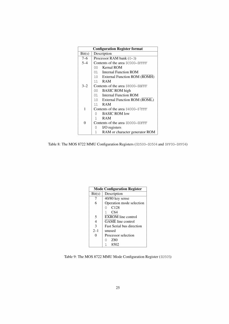
The Mode Configuration Register (Table 9) lets you to change processors and operating modes, among others. Allbits in this register act as outputs, but they can be used as inputs, too. If you wrote a ‘1’ to any bit, external hardwarecould pull the line down, and the bit would output ‘0’. For instance, you can make the operating system to thinkthat the 40/80 key is depressed by clearing the high bit of this register. Also, if you make your own routine to selectthe C64 mode, you will able to assert the EXROM or GAME, if you want to play with different C64 mode memoryconfigurations without having to hook anything to the computer. Also, note that you can use other banks than thedefault 0 in the C64 mode, if you disable common memory and remember to select the video bank.
The 64 kB video bank can be selected with the RAM Configuration Register (Table 10). Its other purpose isselecting the size and location of the Common RAM block, a memory area that defaults to bank 0 in spite of theprocessor RAM bank settings in the Configuration Registers.
Finally, the page relocation registers let you to relocate the processor pages zero and one (addresses $00–$FF and$100–$1FF) anywhere in the memory. Well, actually the 8502’s addresses 0 and 1 always map to its built-in I/Oregister. In addition to that, the MMU defaults the page relocation bank to 0 if you are using common memory atbottom of memory. To relocate the zero page, first write the memory bank (0–3) to $D508, and then write the memorypage number to ($D507). The stack page (page 1) uses the addresses $D509 and $D50A.
3.7 Hints for programming in C128 mode Machine LanguageIt is best to use sixteen or thirty-two kilobytes of common memory on the MMU when using the PIA expansion. Thisway you can hold your program in bank 0 in the lowmost or highmost sixteen kilobytes, or both, and you can easily
24
Configuration Register formatBit(s) Description7–6 Processor RAM bank (0–3)5–4 Contents of the area $C000–$FFFF
00 Kernal ROM01 Internal Function ROM10 External Function ROM (ROMH)11 RAM
3–2 Contents of the area $8000–$BFFF00 BASIC ROM high01 Internal Function ROM10 External Function ROM (ROML)11 RAM
1 Contents of the area $4000–$7FFF0 BASIC ROM low1 RAM
0 Contents of the area $D000–$DFFF0 I/O registers1 RAM or character generator ROM
Table 8: The MOS 8722 MMU Configuration Registers ($D500–$D504 and $FF00–$FF04)
Mode Configuration RegisterBit(s) Description
7 40/80 key sense6 Operation mode selection
0 C1281 C64
5 EXROM line control4 GAME line control3 Fast Serial bus direction
2–1 unused0 Processor selection
0 Z801 8502
Table 9: The MOS 8722 MMU Mode Configuration Register ($D505)
25
RAM Configuration RegisterBits Function7–6 Video RAM bank (0–3)5–4 RAM block (0–3)3–2 Common RAM selection
00 Common RAM block disabled01 Common RAM block at bottom of memory10 Common RAM block at top of memory11 Common RAM block at both top and bottom
1–0 Size of Common RAM block00 1 kB01 4 kB10 8 kB11 16 kB
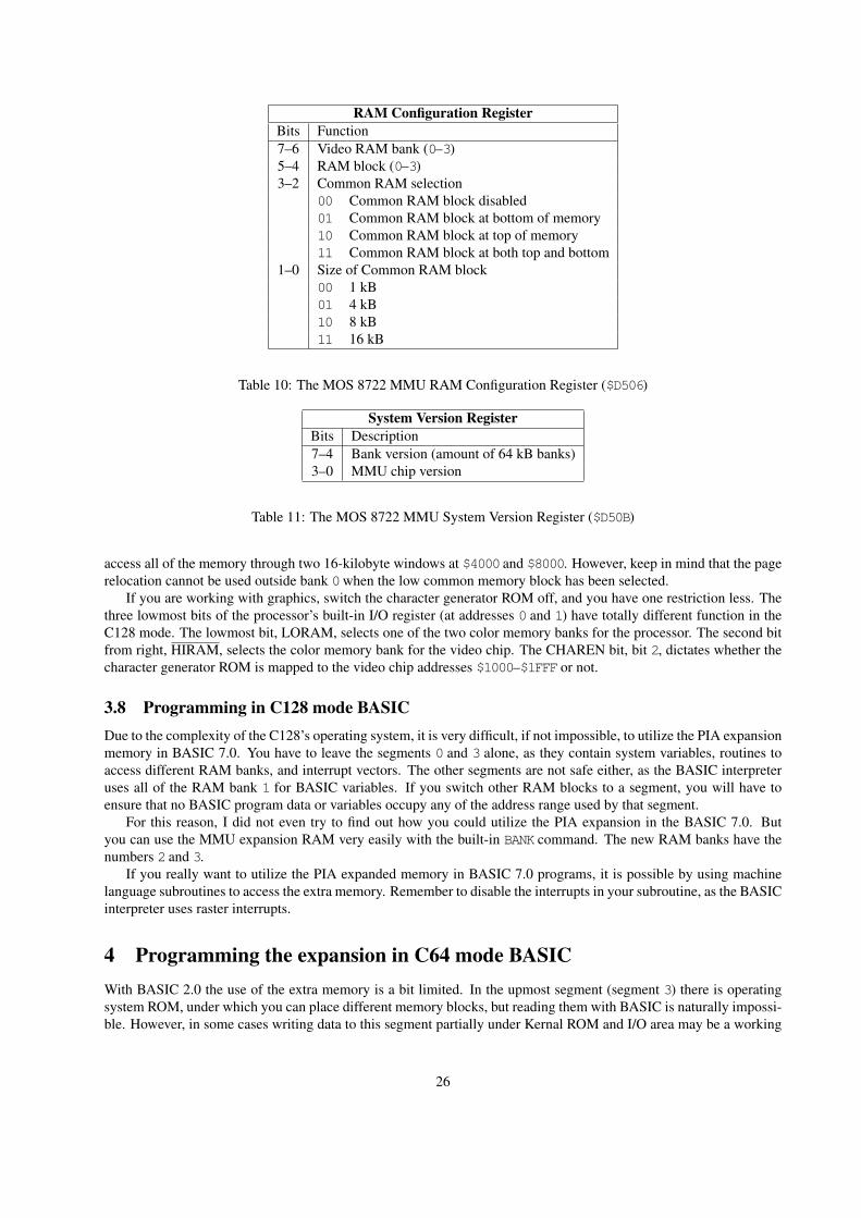
Table 10: The MOS 8722 MMU RAM Configuration Register ($D506)
System Version RegisterBits Description7–4 Bank version (amount of 64 kB banks)3–0 MMU chip version
Table 11: The MOS 8722 MMU System Version Register ($D50B)
access all of the memory through two 16-kilobyte windows at $4000 and $8000. However, keep in mind that the pagerelocation cannot be used outside bank 0 when the low common memory block has been selected.
If you are working with graphics, switch the character generator ROM off, and you have one restriction less. Thethree lowmost bits of the processor’s built-in I/O register (at addresses 0 and 1) have totally different function in theC128 mode. The lowmost bit, LORAM, selects one of the two color memory banks for the processor. The second bitfrom right, HIRAM, selects the color memory bank for the video chip. The CHAREN bit, bit 2, dictates whether thecharacter generator ROM is mapped to the video chip addresses $1000–$1FFF or not.
3.8 Programming in C128 mode BASICDue to the complexity of the C128’s operating system, it is very difficult, if not impossible, to utilize the PIA expansionmemory in BASIC 7.0. You have to leave the segments 0 and 3 alone, as they contain system variables, routines toaccess different RAM banks, and interrupt vectors. The other segments are not safe either, as the BASIC interpreteruses all of the RAM bank 1 for BASIC variables. If you switch other RAM blocks to a segment, you will have toensure that no BASIC program data or variables occupy any of the address range used by that segment.
For this reason, I did not even try to find out how you could utilize the PIA expansion in the BASIC 7.0. Butyou can use the MMU expansion RAM very easily with the built-in BANK command. The new RAM banks have thenumbers 2 and 3.
If you really want to utilize the PIA expanded memory in BASIC 7.0 programs, it is possible by using machinelanguage subroutines to access the extra memory. Remember to disable the interrupts in your subroutine, as the BASICinterpreter uses raster interrupts.
4 Programming the expansion in C64 mode BASICWith BASIC 2.0 the use of the extra memory is a bit limited. In the upmost segment (segment 3) there is operatingsystem ROM, under which you can place different memory blocks, but reading them with BASIC is naturally impossi-ble. However, in some cases writing data to this segment partially under Kernal ROM and I/O area may be a working
26
solution. The lowmost kilobytes are free RAM, and it can be utilized by switching memory blocks. But the benefit ofthe extra memory decreases, as you can use only the lowmost four kilobytes of each block.21
The highest segment but one, segment 2, is halfly under BASIC ROM, and only its lower half can be freely used.22
When utilizing it, you have to take in consideration that those 8 kilobytes can be under a ROM module, if one isconnected, or they could hold some of the variables and tables that are stored in the top of the BASIC memory. Youhave to construct your programs so that they do not collide with the segment’s area.
The lowmost segment, segment 0, contains Kernal’s and BASIC interpreter’s system variables. Normally youcannot change its contents, since the operating system would not find its status information. This can be workedaround by copying those vital bytes to the new memory block and switching the block with a machine languageroutine.
The only segment that can be wholly used with plain BASIC is the segment 1, the second one from the bottom($4000–$7FFF). It resides in the middle of the space reserved for BASIC programs. If you construct your BASICprograms wisely, that is short enough, and ensure that the information used by BASIC are located exactly on this area,you can switch the blocks in this segment freely and exploit all the twelwe extra blocks as a huge data storage.
Example 4.1 shows how you can create a table on this area and hold its data simultaneously in all the extra memoryblocks.
4.1 Processing a huge array10 I=0:J=0:K=0:A=020 DD=56576:PIA=5728030 FOR I=11 TO 0 STEP -1:READ A:POKE PIA,A:NEXT31 DATA 4,254,4,220,0,255,0,255,4,254,52,22040 K=16384-7:POKE 47,K AND 255:POKE 48,K/256:
POKE 49,K AND 255:POKE 50,K/25650 DIM A%(8191)60 FOR I=0 TO 15:POKE PIA,I*16+1270 PRINT I":";:FOR J=0 TO 9:PRINT A%(J),:NEXT:PRINT:NEXT80 POKE PIA,220:END
The program displays ten first integers of each memory block. The table it reserves fills the whole segment 1,because each integer (notice the % sign) takes two bytes and 8192 of them are reserved. The contents of the table A%can be changed to another memory block by simply POKEing PIA’s corresponding register. On the line 40 the table isensured to start at $4000 by changing the start and end addresses of tables in the addresses 47–50. Saving the name,size and dimensions of the table takes the seven bytes, which are subtracted from the start address.
Reserving the table to an arbitrary address has its drawbacks. The size of the program and its variables may notexceed 14 kilobytes so that they could fit to the memory before the beginning of the table. All variables must definitelybe declared before allocating the table. If you do not declare them by giving them a value, the interpreter finds reallyexotic values for them or transfers the table off its position.
4.2 Storing graphics10 I=0:J=0:A=0:A$=""20 DD=56576:PIA=57280:V=53248:COLOUR=5017630 FOR I=11 TO 0 STEP -1:READ A:POKE PIA,A:NEXT31 DATA 4,254,4,220,0,255,0,255,4,254,52,22040 POKE V+24,16+8:POKE V+17,5950 FOR I=0 TO 11:POKE PIA+2,I*16+14:
POKE DD,PEEK(DD) AND 252 OR (NOT I AND 3)60 FOR J=0 TO 999:POKE J+COLOUR,3:NEXT70 GET A$:IF A$="" THEN 70
21 You can read and write the area $C000–$DFFF of this segment using BASIC. Accessing the area $D000–$DFFF without machine language istricky but possible.
22 You can always write under ROM (except in the UltiMax game cartridge configuration).
27
80 NEXT I90 POKE PIA+2,254:POKE DD,PEEK(DD) OR 3:
POKE V+24,23:POKE V+17,27
The extra memory can be used as a store of high resolution pictures as well. This program shows all twelvememory areas that could contain reasonable pictures. The pictures can be created with a BASIC extension that residesin RAM and saves its graphics under Kernal ROM. In those memory blocks that contain no pictures, you see randommemory contents.
High resolution graphics is enabled on the line 40. The beginning of the line 50 switches block I to the segment 3and switches the VIC chip to the same memory area. The second POKE statement selects the block for the video chip.‘(NOT I AND 3)’ filters the extra bits off and inverts the essential ones so that they can be stored to the lowmost twobits of $DD00. The line 60 sets the picture’s colour to black-cyan. The next line waits for a keystroke before showinganother picture. After all blocks have been shown, the original state of the I/O chips will be restored on the line 90.
5 RAM disk and other C64 mode programsAs memory expansions are expensive, programs making use of extra memory are rare. Besides, different expansionsare not compatible with each other. However, it does not mean that you could not fully utilize the expansion. The mostobvious utilization method is a RAM disk. When using VC-1541, it is not only luxury but almost vital condition.
Pekka Pessi has made a couple of C64 programs that utilize the PIA expansion. The software is distributed in twoself-extracting archive files (SFXes).
The file ROS-V1.SFX (for RAM Operating System) holds the source code of the RAM disk program, and somemiscellanous files. To load the archive file, use the command “LOAD"ROS-V1.SFX",device”. Then change a blankdisk to the drive before RUNning. The second archive file, UTIL256.SFX, contains the following software:
5.1 Memory testThe program TEST tests the block selection and the whole memory. If it jams before reporting “Test passed”,something has gone wrong. Its source code is in the file TEST.A, which requires a library STRING.A. I translated theexecutable to English by patching the binary file.
5.2 Poor man’s multitaskingWith the MULTI51200 program you can run four different programs. The program does no multitasking, it only holdsfour environments in the memory, each in its own memory block. MULTI.A is the source code. After loading it with“LOAD"MULTI51200",device,1” and initializing the BASIC pointers with “NEW”, you can switch the environmentswith “SYS51200,f,b”. The parameter f is a flag determining if the current block should be copied to the destinationblock (0) or not (1). The b selects the destination block (0–3). The initial block is 3.
5.3 Machine language monitorIf you don’t like to switch the memory blocks manually in your favourite machine language monitor, the MON256 utilityis for you. The memory is again divided to four 64 kB blocks, numbered from 0 to 3. The commands are explained inTable 12.
The source code for the monitor is split in the files MON.A, CONSOLE.A, COM.A, ROUTINES.A and TABELS.A.
5.4 RAM diskThe most important utility is a RAM disk program, which occupies about 9 kilobytes of memory. It transfers Kernaland BASIC interpreter to RAM and patches the serial bus routines. The actual program is in the area $00800–$03FFF.
It emulates all VC-1541 functions except relative files. For example, the commands U1, U2, B-A etc. work. UI+and UI- make no difference. The program also detects some fast loaders and works with them installed.
The loader is called RAM DISC, and the patched Kernal is in RAM.K. You need only patches to the low-level serialbus routines, so you may want to restore the original colors and keyboard definitions. To minimize incompatibility
28
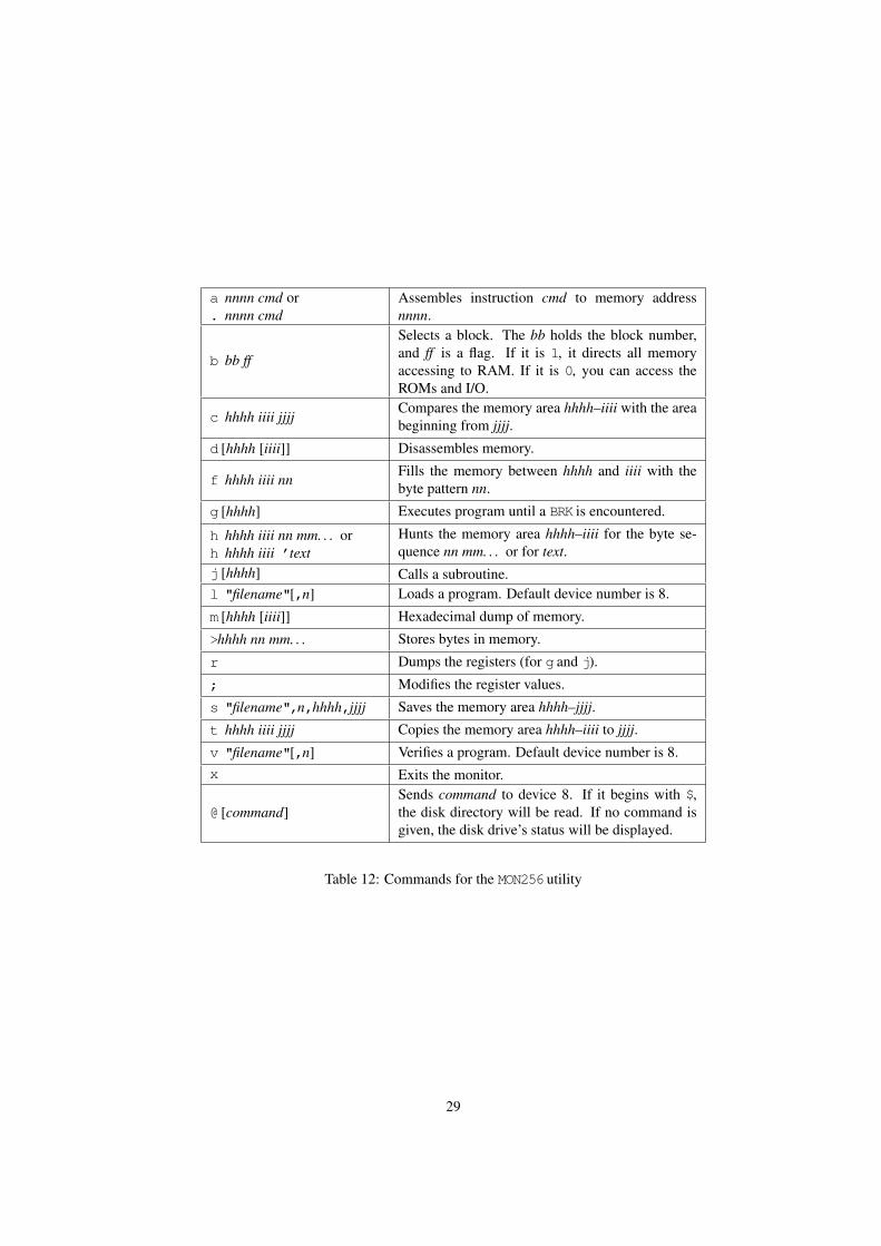
a nnnn cmd or. nnnn cmd
Assembles instruction cmd to memory addressnnnn.
b bb ff
Selects a block. The bb holds the block number,and ff is a flag. If it is 1, it directs all memoryaccessing to RAM. If it is 0, you can access theROMs and I/O.
c hhhh iiii jjjjCompares the memory area hhhh–iiii with the areabeginning from jjjj.
d [hhhh [iiii]] Disassembles memory.
f hhhh iiii nnFills the memory between hhhh and iiii with thebyte pattern nn.
g [hhhh] Executes program until a BRK is encountered.
h hhhh iiii nn mm. . . orh hhhh iiii ’text
Hunts the memory area hhhh–iiii for the byte se-quence nn mm. . . or for text.
j [hhhh] Calls a subroutine.l "filename"[,n] Loads a program. Default device number is 8.
m [hhhh [iiii]] Hexadecimal dump of memory.
>hhhh nn mm. . . Stores bytes in memory.
r Dumps the registers (for g and j).
; Modifies the register values.
s "filename",n,hhhh,jjjj Saves the memory area hhhh–jjjj.
t hhhh iiii jjjj Copies the memory area hhhh–iiii to jjjj.
v "filename"[,n] Verifies a program. Default device number is 8.x Exits the monitor.
@ [command]Sends command to device 8. If it begins with $,the disk directory will be read. If no command isgiven, the disk drive’s status will be displayed.
Table 12: Commands for the MON256 utility
29
problems, you should replace the ROM chip that holds the BASIC and Kernal ROMs with an EPROM containing thepatched Kernal. The RAM disk routines are in RAM.C.
5.4.1 Disk copiers
The program RAM DISC COPY copies a regular 1541 disk to RAM. It utilizes the slow U1 command, and it is includedas an example only. The source code DUP.A exposes the RAM disk’s storage format.
A faster and more useful tool is FDUPLICATE. Using it, you can copy a regular disk to the RAM disk or vice versa.You can make multiple copies of a disk easily. This program’s fast transfer routines are designed for PAL systems,and the utility cannot be used in NTSC machines without little modification. Its source code is in the two files S/SUCKand S/DSUCK.
6 Enhancing the PIA expansionThere are a couple of unused contacts in the PIA. In addition to that, two 7405 ports are not connected. The extra PIAlines include an input, CB1, an input/output line CB2, and the Interrupt Request line IRQB.
If you connect the IRQB line to the IRQ or NMI input of your system, you can have one or two new interruptsources, useful for interfacing your custom hardware. And if you are running out of User Port pins, the lines CB1 andCB2 can save you from designing an I/O cartridge. Besides, you can use the IRQB as an output if you wire the CB1line to something that you can control with software, CA2 for instance. Just remember to add a pull-up resistor to theIRQB line if necessary.
6.1 Built-in freezerFor the Commodore 64, there are several ‘freezer’ cartridges that let the user to halt theoretically any program (game)to alter it (make the player immortal), or more often merely to make a ‘back-up copy’ of it. Alas, anything cannot befrozen with these cartridges. If the programmer of the game is clever enough to inhibit IRQ and NMI interrupts in hisprogram, and if the code runs at the area $0000–$0FFF, no external cartridge will be able to halt it without assertingthe RESET signal, which would lose most status information of the computer.
You can use the PIA expansion to freeze programs, in many cases also in the C128 mode. In the C64 mode, aninternal freezer can stop anything except a totally jammed program. In the C128 mode, it can stop software runningon the 8502 without using any ROM at the area $C000–$FFFF.
This freezer expansion will let you to replace the program’s memory with previously initialized RAM by pressingthe Restore key. If the NMI interrupts are disabled, freezing will be done with the BRK instruction. As the circuitforces the HIRAM line to logical zero, the C64 mode interrupt vectors will always be fetched from RAM. All of thefreezer software can be stored to RAM, so it is easy to change, and no EPROM programming devices are needed.Another advantage is that the freezer software may freely use 128 kilobytes of memory, and there are 64 kilobytesof working storage, way more than in the best freezer cartridges. Besides, those amounts will be at least doubled orquadrupled in the C128 mode freezer, depending on whether you have built the MMU expansion.
For this expansion, you need a double ON–OFF or ON–ON switch, four 1N4148 diodes and two 10 kΩ resistors.First do some preparations. Break the connection between the PIA’s RESET input (pin 34) and the system RESET,and replace it with a diode with the marked end towards the system bus, so that the pass direction is from the PIA tothe system RESET. Then you have to solder a pull-up resistor between the PIA’s RESET line and the +5 V poweroutlet. Locate the U29 chip (7406) on the motherboard and desolder its pin 4. Solder a diode between the motherboardconnection and the pin with the mark pointing to the chip. Finally, solder the other pull-up resistor between the U29’spin 4 and +5 V. After these modifications, the PIA should continue to reset normally, and the Restore key shouldremain functional.
Now you can mount the switch to the system. If you have an ON–ON switch, hold it in your hand in such an anglethat you see two rows of three pins. Solder two diodes from the right-hand contacts of the switch to the U29’s pin 4,with the mark pointing to the U29. Solder the PIA’s RESET line (pin 34) to either middle contact of the switch, or toeither free contact if you have an ON–OFF switch. Finally, mount the HIRAM line, which is on the 8502’s pin 29, tothe remaining middle contact.
The switch affects in the operation of the Restore key. When it is open, the Restore key operates normally. Whenthe switch is closed, the Restore key also resets the PIA, switching the default memory blocks in, and forces the
30
HIRAM line low, so that the interrupt vectors will always be fetched from RAM. The idea of the expansion is that theprogram runs in some other memory blocks, say 3–0, with the PIA totally disabled from the address space. The defaultmemory blocks ($F–$C) will be initialized mostly with null bytes, which is the opcode of the BRK instruction. You alsoneed the freezer interrupt vectors ($FFFA–$FFFF) and a small interrupt handler that stores the processor registers andswitches the main freezer program into the address space.
If you want to freeze hanged programs, too, you can do it without losing the state of the I/O chips. By using acustom Kernal ROM, you could even store all 8502 registers except the Program Counter. You just have to be ableto reset the 8502 without resetting the rest of the chips. To do this, desolder the RESET signal, pin 40 on the 8502.Connect a 1N4148 diode between the system RESET signal and the 8502, with the mark pointing away from theprocessor. Add a pull-up resistor to the signal, and a switch between the logical ground and the signal.
Now, whenever you push the switch, only the 8502 will be reset. If the computer is in the C64 mode at this time,it will remain in that mode, since the MMU does not get reset. You should then use the Autostart code ($C3 $C2 $CD$38 $30 at $8004–$8008), and the Kernal will jump to the vector ($8000). Unfortunately it will destroy all registersexcept the Y register when searching for that code. More fortunately, if the computer is in the C128 mode, and if theKernal ROM is not selected in the memory configuration, the processor will fetch the RESET vector from the activeRAM bank. In that case you can store all processor registers except the program counter.
Alas, I just have invented a software hack that cannot be frozen with this circuit. If a program runs on the I/O area($DE00–$DFFF except the range where the PIA is mapped to while the I/O is switched on) and has disabled the NMIinterrupts, the program will continue running even if you have activated the freezer and hit the Restore key. Shouldyou ever encounter this type of a software hack, you can use a triple switch and add the LORAM signal (8502’s pin 30)to one extra contact. Connect the remaining contact to the U29’s pin 4 through a diode with the mark pointing to theU29. This will disable the I/O area for the time the Restore signal is active, so the processor can fetch a BRK from thememory underneath, and will always freeze correctly.
I haven’t completed the freezer expansion yet, as the daughter-board in my faithful 2564 (C64 with the 256 kBexpansion) stopped working when I opened the cover to start the surgery operation. My first attempt of rebuilding itdid not succeed, and now I am in Germany, more than one megameter away from the computer. When returning toFinland in August 1994, the freezer expansion will be one of my first projects I am going to finish.23
Naturally you also need a program to utilize the freezer circuitry. You don’t need to code so much, only the routineto jump back to the freezed program and the routine that saves all registers upon freezing need to be written fromscratch. You can patch existing machine language monitors, sprite editors and utilities like that, only the data fetchand data store subroutines must be rewritten. Developing the freezer software is very simple, since you can access thefrozen program through a 16 kB window, and you can use the Kernal routines all the time.
6.2 New operating systemIn my C64, I have replaced the 2364 Kernal ROM with a 32-kilobyte EPROM. The two extra address lines arecontrolled by the PIA’s pins CA2 and CB2. As the C128 uses a 23128 ROM for both C64 BASIC ROM and KernalROM, this type of expansion cannot be used. Besides, you can access only 256 kilobytes of the memory in the C64mode. Why would you want to improve the C64 mode if you can make the C128 mode far better?
The C128 has a socket for a Function ROM for your operating system extensions. It can hold a 27256 EPROM,32 kilobytes. If that does not satisfy your needs, you could use a 27512 EPROM instead. In this case you have to bendthe A15 line up. This line could be controlled by the PIA’s CB2 line. To ensure that the logic works also when theCB2 line is input, add a 4.7 kΩ pull-up resistor between CB2 and +5 V.
23 So I thought at that time—as of December 1999, I have neither fixed that particular C64 nor completed the freezer expansion. Besides, theexpansion would not have much advantage over freezer cartridges or the features present in some emulators.
31
Related Documents


