MELSEC-L Digital-Analog Converter Module User's Manual -L60DA4 -L60DAVL8 -L60DAIL8

Welcome message from author
This document is posted to help you gain knowledge. Please leave a comment to let me know what you think about it! Share it to your friends and learn new things together.
Transcript
MELSEC-L Digital-Analog Converter Module User's Manual
-L60DA4-L60DAVL8-L60DAIL8

SAFETY PRECAUTIONS(Read these precautions before using this product.)
Before using this product, please read this manual and the relevant manuals carefully and pay full attention
to safety to handle the product correctly.
The precautions given in this manual are concerned with this product only. For the safety precautions of the
programmable controller system, refer to the user's manual for the CPU module used.
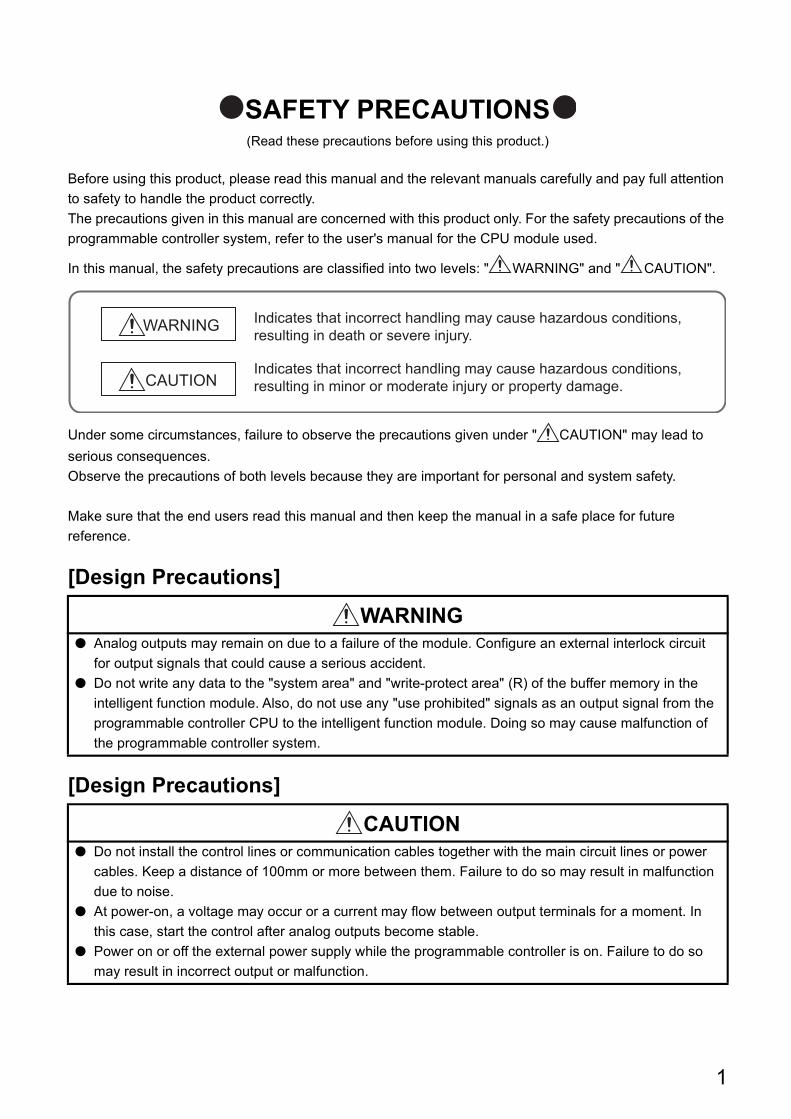
In this manual, the safety precautions are classified into two levels: " WARNING" and " CAUTION".
Under some circumstances, failure to observe the precautions given under " CAUTION" may lead to
serious consequences.
Observe the precautions of both levels because they are important for personal and system safety.
Make sure that the end users read this manual and then keep the manual in a safe place for future
reference.
[Design Precautions]
[Design Precautions]
WARNING● Analog outputs may remain on due to a failure of the module. Configure an external interlock circuit
for output signals that could cause a serious accident.
● Do not write any data to the "system area" and "write-protect area" (R) of the buffer memory in the
intelligent function module. Also, do not use any "use prohibited" signals as an output signal from the
programmable controller CPU to the intelligent function module. Doing so may cause malfunction of
the programmable controller system.
CAUTION● Do not install the control lines or communication cables together with the main circuit lines or power
cables. Keep a distance of 100mm or more between them. Failure to do so may result in malfunction
due to noise.
● At power-on, a voltage may occur or a current may flow between output terminals for a moment. In
this case, start the control after analog outputs become stable.
● Power on or off the external power supply while the programmable controller is on. Failure to do so
may result in incorrect output or malfunction.
WARNING
CAUTION
Indicates that incorrect handling may cause hazardous conditions,resulting in death or severe injury.
Indicates that incorrect handling may cause hazardous conditions, resulting in minor or moderate injury or property damage.
1
[Installation Precautions]
[Installation Precautions]
[Wiring Precautions]
WARNING● Shut off the external power supply (all phases) used in the system before mounting or removing a
module. Failure to do so may result in electric shock or cause the module to fail or malfunction.
CAUTION● Use the programmable controller in an environment that meets the general specifications in the Safety
Guidelines provided with the CPU module or head module. Failure to do so may result in electric
shock, fire, malfunction, or damage to or deterioration of the product.
● To interconnect modules, engage the respective connectors and securely lock the module joint levers
until they click. Incorrect interconnection may cause malfunction, failure, or drop of the module.
● Tighten the screws within the specified torque range. Undertightening can cause drop of the screw,
short circuit, or malfunction. Overtightening can damage the screw and/or module, resulting in drop,
short circuit, or malfunction.
● Do not directly touch any conductive parts and electronic components of the module. Doing so can
cause malfunction or failure of the module.
WARNING● After installation and wiring, attach the included terminal cover to the module before turning it on for
operation. Failure to do so may result in electric shock.
2
[Wiring Precautions]
[Startup and Maintenance Precautions]
[Startup and Maintenance Precautions]
CAUTION● Individually ground the FG terminal of the programmable controller with a ground resistance of 100
ohms or less. Failure to do so may result in electric shock or malfunction.
● Tighten the terminal block screws within the specified torque range. Undertightening can cause short
circuit, fire, or malfunction. Overtightening can damage the screw and/or module, resulting in drop,
short circuit, or malfunction.
● Prevent foreign matter such as dust or wire chips from entering the module. Such foreign matter can
cause a fire, failure, or malfunction.
● A protective film is attached to the top of the module to prevent foreign matter, such as wire chips,
from entering the module during wiring. Do not remove the film during wiring. Remove it for heat
dissipation before system operation.
● Mitsubishi Electric programmable controllers must be installed in control panels. Connect the main
power supply to the power supply module in the control panel through a relay terminal block. Wiring
and replacement of a power supply module must be performed by qualified maintenance personnel
with knowledge of protection against electric shock. For wiring methods, refer to the MELSEC-L CPU
Module User's Manual (Hardware Design, Maintenance and Inspection).
WARNING● Do not touch any terminal while power is on. Doing so will cause electric shock or malfunction.
● Shut off the external power supply (all phases) used in the system before cleaning the module or
retightening the terminal block screws. Failure to do so may result in electric shock.
CAUTION● Do not disassemble or modify the module. Doing so may cause failure, malfunction, injury, or a fire.
● Shut off the external power supply (all phases) used in the system before mounting or removing a
module. Failure to do so may cause the module to fail or malfunction.
● Tighten the terminal block screws within the specified torque range. Undertightening can cause drop
of the screw, short circuit, or malfunction. Overtightening can damage the screw and/or module,
resulting in drop, short circuit, or malfunction.
● After the first use of the product (module, display unit, and terminal block), the number of
connections/disconnections is limited to 50 times (in accordance with IEC 61131-2). Exceeding the
limit may cause malfunction.
● Before handling the module, touch a conducting object such as a grounded metal to discharge the
static electricity from the human body. Failure to do so may cause the module to fail or malfunction.
3
[Disposal Precautions]
CAUTION● When disposing of this product, treat it as industrial waste.
4
CONDITIONS OF USE FOR THE PRODUCT(1) Mitsubishi programmable controller ("the PRODUCT") shall be used in conditions;
i) where any problem, fault or failure occurring in the PRODUCT, if any, shall not lead to any major
or serious accident; and
ii) where the backup and fail-safe function are systematically or automatically provided outside of
the PRODUCT for the case of any problem, fault or failure occurring in the PRODUCT.
(2) The PRODUCT has been designed and manufactured for the purpose of being used in general
industries.
MITSUBISHI SHALL HAVE NO RESPONSIBILITY OR LIABILITY (INCLUDING, BUT NOT
LIMITED TO ANY AND ALL RESPONSIBILITY OR LIABILITY BASED ON CONTRACT,
WARRANTY, TORT, PRODUCT LIABILITY) FOR ANY INJURY OR DEATH TO PERSONS OR
LOSS OR DAMAGE TO PROPERTY CAUSED BY the PRODUCT THAT ARE OPERATED OR
USED IN APPLICATION NOT INTENDED OR EXCLUDED BY INSTRUCTIONS, PRECAUTIONS,
OR WARNING CONTAINED IN MITSUBISHI'S USER, INSTRUCTION AND/OR SAFETY
MANUALS, TECHNICAL BULLETINS AND GUIDELINES FOR the PRODUCT.
("Prohibited Application")
Prohibited Applications include, but not limited to, the use of the PRODUCT in;
• Nuclear Power Plants and any other power plants operated by Power companies, and/or any
other cases in which the public could be affected if any problem or fault occurs in the PRODUCT.
• Railway companies or Public service purposes, and/or any other cases in which establishment of
a special quality assurance system is required by the Purchaser or End User.
• Aircraft or Aerospace, Medical applications, Train equipment, transport equipment such as
Elevator and Escalator, Incineration and Fuel devices, Vehicles, Manned transportation,
Equipment for Recreation and Amusement, and Safety devices, handling of Nuclear or
Hazardous Materials or Chemicals, Mining and Drilling, and/or other applications where there is a
significant risk of injury to the public or property.
Notwithstanding the above, restrictions Mitsubishi may in its sole discretion, authorize use of the
PRODUCT in one or more of the Prohibited Applications, provided that the usage of the PRODUCT
is limited only for the specific applications agreed to by Mitsubishi and provided further that no
special quality assurance or fail-safe, redundant or other safety features which exceed the general
specifications of the PRODUCTs are required. For details, please contact the Mitsubishi
representative in your region.
5
INTRODUCTION
Thank you for purchasing the Mitsubishi Electric MELSEC-L series programmable controllers.
This manual describes the functions and programming of a digital-analog converter module (hereafter abbreviated as
D/A converter module).
Before using this product, please read this manual and the relevant manuals carefully and develop familiarity with the
functions and performance of the MELSEC-L series programmable controller to handle the product correctly.
When applying the program examples introduced in this manual to an actual system, ensure the applicability and
confirm that it will not cause system control problems.
Relevant module: L60DA4, L60DAVL8, L60DAIL8
Remark
● Unless otherwise specified, this manual describes the program examples in which the I/O numbers of X/Y00 to X/Y0F are assigned for a D/A converter module.For I/O number assignment, refer to the following.
MELSEC-L CPU Module User's Manual (Function Explanation, Program Fundamentals)
● Operating procedures are explained using GX Works2. When using GX Developer or GX Configurator-DA, refer to the following.
• When using GX Developer or GX Configurator-DA ( Page 237, Appendix 9)
6
COMPLIANCE WITH EMC AND LOW VOLTAGE DIRECTIVES
(1) Method of ensuring complianceTo ensure that Mitsubishi Electric programmable controllers maintain EMC and Low Voltage Directives when
incorporated into other machinery or equipment, certain measures may be necessary. Please refer to one of the
following manuals.
• MELSEC-L CPU Module User's Manual (Hardware Design, Maintenance and Inspection)
• MELSEC-L CC-Link IE Field Network Head Module User's Manual
• Safety Guidelines (This manual is included with the CPU module or head module.)
The CE mark on the side of the programmable controller indicates compliance with EMC and Low Voltage
Directives.
(2) Additional measuresNo additional measures are necessary for the compliance of this product with the EMC and Low Voltage
Directives.
7
RELEVANT MANUALS
(1) CPU module user's manual
(2) Head module User's Manual
(3) Operating manual
Manual name
<manual number (model code)>Description
MELSEC-L CPU Module User's Manual (Hardware Design, Maintenance and
Inspection)
<SH-080890ENG, 13JZ36>
Specifications of the CPU modules, power supply modules, display unit,
branch module, extension module, SD memory cards, and batteries,
information on how to establish a system, maintenance and inspection, and
troubleshooting
MELSEC-L CPU Module User's Manual (Function Explanation, Program
Fundamentals)
<SH-080889ENG, 13JZ35>
Functions and devices of the CPU module, and programming
Manual name
<manual number (model code)>Description
MELSEC-L CC-Link IE Field Network Head Module User's Manual
<SH-080919ENG, 13JZ48>
Specifications, procedures before operation, system configuration, installation,
wiring, settings, and troubleshooting of the head module
MELSEC-Q CC-Link IE Field Network Master/Local Module User's Manual
<SH-080917ENG, 13JZ47>
Overview of the CC-Link IE Field Network, and specifications, procedures
before operation, system configuration, installation, settings, functions,
programming, and troubleshooting of the CC-Link IE Field Network
master/local module
Manual name
<manual number (model code)>Description
GX Works2 Version 1 Operating Manual (Common)
<SH-080779ENG, 13JU63>
System configuration, parameter settings, and online operations of GX
Works2, which are common to Simple projects and Structured projects
GX Developer Version 8 Operating Manual
<SH-080373E, 13JU41>
Operating methods of GX Developer, such as programming, printing,
monitoring, and debugging
8

Memo
9
CONTENTS
10
CONTENTS
SAFETY PRECAUTIONS . . . . . . . . . . . . . . . . . . . . . . . . . . . . . . . . . . . . . . . . . . . . . . . . . . . . . . . . . . . . . 1CONDITIONS OF USE FOR THE PRODUCT . . . . . . . . . . . . . . . . . . . . . . . . . . . . . . . . . . . . . . . . . . . . . 5
INTRODUCTION . . . . . . . . . . . . . . . . . . . . . . . . . . . . . . . . . . . . . . . . . . . . . . . . . . . . . . . . . . . . . . . . . . . . 6COMPLIANCE WITH EMC AND LOW VOLTAGE DIRECTIVES . . . . . . . . . . . . . . . . . . . . . . . . . . . . . . . 7RELEVANT MANUALS . . . . . . . . . . . . . . . . . . . . . . . . . . . . . . . . . . . . . . . . . . . . . . . . . . . . . . . . . . . . . . . 8MANUAL PAGE ORGANIZATION . . . . . . . . . . . . . . . . . . . . . . . . . . . . . . . . . . . . . . . . . . . . . . . . . . . . . . 13TERMS . . . . . . . . . . . . . . . . . . . . . . . . . . . . . . . . . . . . . . . . . . . . . . . . . . . . . . . . . . . . . . . . . . . . . . . . . . 18PACKING LIST . . . . . . . . . . . . . . . . . . . . . . . . . . . . . . . . . . . . . . . . . . . . . . . . . . . . . . . . . . . . . . . . . . . . 18
CHAPTER 1 D/A CONVERTER MODULE 19
1.1 Application . . . . . . . . . . . . . . . . . . . . . . . . . . . . . . . . . . . . . . . . . . . . . . . . . . . . . . . . . . . . . . . . 19
1.2 Features . . . . . . . . . . . . . . . . . . . . . . . . . . . . . . . . . . . . . . . . . . . . . . . . . . . . . . . . . . . . . . . . . . 20
CHAPTER 2 PART NAMES 21
CHAPTER 3 SPECIFICATIONS 23
3.1 General Specifications . . . . . . . . . . . . . . . . . . . . . . . . . . . . . . . . . . . . . . . . . . . . . . . . . . . . . . . 23
3.2 Performance Specifications . . . . . . . . . . . . . . . . . . . . . . . . . . . . . . . . . . . . . . . . . . . . . . . . . . . 24
3.2.1 Number of parameter settings . . . . . . . . . . . . . . . . . . . . . . . . . . . . . . . . . . . . . . . . . . . . . . . . .27
3.3 Function List . . . . . . . . . . . . . . . . . . . . . . . . . . . . . . . . . . . . . . . . . . . . . . . . . . . . . . . . . . . . . . . 28
3.4 I/O Signal List . . . . . . . . . . . . . . . . . . . . . . . . . . . . . . . . . . . . . . . . . . . . . . . . . . . . . . . . . . . . . . 29
3.5 List of Buffer Memory Address . . . . . . . . . . . . . . . . . . . . . . . . . . . . . . . . . . . . . . . . . . . . . . . . . 30
CHAPTER 4 PROCEDURES BEFORE STARTING THE OPERATION 42
CHAPTER 5 SYSTEM CONFIGURATION 44
5.1 Overall System Configuration . . . . . . . . . . . . . . . . . . . . . . . . . . . . . . . . . . . . . . . . . . . . . . . . . . 44
5.2 Applicable System . . . . . . . . . . . . . . . . . . . . . . . . . . . . . . . . . . . . . . . . . . . . . . . . . . . . . . . . . . 45
5.3 Restrictions When D/A Converter Module is Connected to Head Module . . . . . . . . . . . . . . . . 45
CHAPTER 6 INSTALLATION AND WIRING 46
6.1 Installation Environment and Installation Position . . . . . . . . . . . . . . . . . . . . . . . . . . . . . . . . . . 46
6.2 Terminal Block . . . . . . . . . . . . . . . . . . . . . . . . . . . . . . . . . . . . . . . . . . . . . . . . . . . . . . . . . . . . . 47
6.3 Wiring . . . . . . . . . . . . . . . . . . . . . . . . . . . . . . . . . . . . . . . . . . . . . . . . . . . . . . . . . . . . . . . . . . . . 50
6.4 External Wiring . . . . . . . . . . . . . . . . . . . . . . . . . . . . . . . . . . . . . . . . . . . . . . . . . . . . . . . . . . . . . 52
CHAPTER 7 VARIOUS SETTINGS 55
7.1 Addition of Modules . . . . . . . . . . . . . . . . . . . . . . . . . . . . . . . . . . . . . . . . . . . . . . . . . . . . . . . . . 55
7.2 Switch Setting . . . . . . . . . . . . . . . . . . . . . . . . . . . . . . . . . . . . . . . . . . . . . . . . . . . . . . . . . . . . . . 56
7.3 Parameter Setting. . . . . . . . . . . . . . . . . . . . . . . . . . . . . . . . . . . . . . . . . . . . . . . . . . . . . . . . . . . 58
7.4 Auto Refresh. . . . . . . . . . . . . . . . . . . . . . . . . . . . . . . . . . . . . . . . . . . . . . . . . . . . . . . . . . . . . . . 59
7.5 Offset/Gain Setting . . . . . . . . . . . . . . . . . . . . . . . . . . . . . . . . . . . . . . . . . . . . . . . . . . . . . . . . . . 60
7.5.1 Setting from "Offset/Gain Setting" of GX Works2. . . . . . . . . . . . . . . . . . . . . . . . . . . . . . . . . . .60
7.5.2 Setting from a program . . . . . . . . . . . . . . . . . . . . . . . . . . . . . . . . . . . . . . . . . . . . . . . . . . . . . .63
CHAPTER 8 FUNCTIONS 67
8.1 Mode. . . . . . . . . . . . . . . . . . . . . . . . . . . . . . . . . . . . . . . . . . . . . . . . . . . . . . . . . . . . . . . . . . . . . 67
8.2 D/A Conversion Enable/Disable Function. . . . . . . . . . . . . . . . . . . . . . . . . . . . . . . . . . . . . . . . . 70
8.3 D/A Output Enable/Disable Function . . . . . . . . . . . . . . . . . . . . . . . . . . . . . . . . . . . . . . . . . . . . 70
8.4 Analog Output HOLD/CLEAR Function . . . . . . . . . . . . . . . . . . . . . . . . . . . . . . . . . . . . . . . . . . 71
8.5 Analog Output Test when CPU Module is in STOP Status . . . . . . . . . . . . . . . . . . . . . . . . . . . . 75
8.6 Scaling function . . . . . . . . . . . . . . . . . . . . . . . . . . . . . . . . . . . . . . . . . . . . . . . . . . . . . . . . . . . . 77
8.7 Warning Output Function . . . . . . . . . . . . . . . . . . . . . . . . . . . . . . . . . . . . . . . . . . . . . . . . . . . . . 83
8.8 Wave Output Function . . . . . . . . . . . . . . . . . . . . . . . . . . . . . . . . . . . . . . . . . . . . . . . . . . . . . . . 86
8.8.1 Initial settings of the wave output function . . . . . . . . . . . . . . . . . . . . . . . . . . . . . . . . . . . . . . . .96
8.8.2 Execution of the wave output function . . . . . . . . . . . . . . . . . . . . . . . . . . . . . . . . . . . . . . . . . .113
8.8.3 Points for the use of the wave output function . . . . . . . . . . . . . . . . . . . . . . . . . . . . . . . . . . . .118
8.8.4 Wave output step action function . . . . . . . . . . . . . . . . . . . . . . . . . . . . . . . . . . . . . . . . . . . . . .126
8.9 Error Log Function . . . . . . . . . . . . . . . . . . . . . . . . . . . . . . . . . . . . . . . . . . . . . . . . . . . . . . . . . 135
8.10 Module Error Collection Function . . . . . . . . . . . . . . . . . . . . . . . . . . . . . . . . . . . . . . . . . . . . . . 138
8.11 Error Clear Function . . . . . . . . . . . . . . . . . . . . . . . . . . . . . . . . . . . . . . . . . . . . . . . . . . . . . . . . 139
8.12 Save/Restoration of Offset/Gain Value . . . . . . . . . . . . . . . . . . . . . . . . . . . . . . . . . . . . . . . . . . 140
CHAPTER 9 DISPLAY UNIT 147
9.1 Display Unit. . . . . . . . . . . . . . . . . . . . . . . . . . . . . . . . . . . . . . . . . . . . . . . . . . . . . . . . . . . . . . . 147
9.2 Menu Structure . . . . . . . . . . . . . . . . . . . . . . . . . . . . . . . . . . . . . . . . . . . . . . . . . . . . . . . . . . . . 147
9.3 List of Setting Value Change Screens . . . . . . . . . . . . . . . . . . . . . . . . . . . . . . . . . . . . . . . . . . 149
9.4 Checking and Clearing Errors. . . . . . . . . . . . . . . . . . . . . . . . . . . . . . . . . . . . . . . . . . . . . . . . . 151
CHAPTER 10 PROGRAMMING 153
10.1 Procedure for Programming . . . . . . . . . . . . . . . . . . . . . . . . . . . . . . . . . . . . . . . . . . . . . . . . . . 153
10.2 When Using the Module in a Standard System Configuration . . . . . . . . . . . . . . . . . . . . . . . . 154
10.3 When D/A Converter Module is Connected to Head Module . . . . . . . . . . . . . . . . . . . . . . . . . 159
CHAPTER 11 TROUBLESHOOTING 167
11.1 Checking on the Module Detailed Information . . . . . . . . . . . . . . . . . . . . . . . . . . . . . . . . . . . . 168
11.2 Checking by Latest Error Code (Un\G19). . . . . . . . . . . . . . . . . . . . . . . . . . . . . . . . . . . . . . . . 169
11.3 Checking on the Module Error Collection Function . . . . . . . . . . . . . . . . . . . . . . . . . . . . . . . . 170
11.4 Error Code List . . . . . . . . . . . . . . . . . . . . . . . . . . . . . . . . . . . . . . . . . . . . . . . . . . . . . . . . . . . . 171
11.5 Alarm Code List . . . . . . . . . . . . . . . . . . . . . . . . . . . . . . . . . . . . . . . . . . . . . . . . . . . . . . . . . . . 174
11.6 Troubleshooting . . . . . . . . . . . . . . . . . . . . . . . . . . . . . . . . . . . . . . . . . . . . . . . . . . . . . . . . . . . 175
11.6.1 Troubleshooting by the LED. . . . . . . . . . . . . . . . . . . . . . . . . . . . . . . . . . . . . . . . . . . . . . . . . .175
11.6.2 Troubleshooting of D/A conversion . . . . . . . . . . . . . . . . . . . . . . . . . . . . . . . . . . . . . . . . . . . .176
11.7 Checking the Status of D/A Converter Module by the System Monitor . . . . . . . . . . . . . . . . . 182
11
12
APPENDICES 183
Appendix 1 Details of I/O Signals. . . . . . . . . . . . . . . . . . . . . . . . . . . . . . . . . . . . . . . . . . . . . . . . . . . 183
Appendix 1.1 Input signal. . . . . . . . . . . . . . . . . . . . . . . . . . . . . . . . . . . . . . . . . . . . . . . . . . . . . . . . .183
Appendix 1.2 Output signal . . . . . . . . . . . . . . . . . . . . . . . . . . . . . . . . . . . . . . . . . . . . . . . . . . . . . . .188
Appendix 2 Details of Buffer Memory Addresses. . . . . . . . . . . . . . . . . . . . . . . . . . . . . . . . . . . . . . . 190
Appendix 3 I/O Conversion Characteristic of D/A Conversion . . . . . . . . . . . . . . . . . . . . . . . . . . . . . 216
Appendix 4 D/A Conversion Accuracy . . . . . . . . . . . . . . . . . . . . . . . . . . . . . . . . . . . . . . . . . . . . . . . 221
Appendix 5 Dedicated Instruction . . . . . . . . . . . . . . . . . . . . . . . . . . . . . . . . . . . . . . . . . . . . . . . . . . 222
Appendix 5.1 Instruction list . . . . . . . . . . . . . . . . . . . . . . . . . . . . . . . . . . . . . . . . . . . . . . . . . . . . . . .222
Appendix 5.2 G(P).OFFGAN . . . . . . . . . . . . . . . . . . . . . . . . . . . . . . . . . . . . . . . . . . . . . . . . . . . . . .223
Appendix 5.3 G(P).OGLOAD . . . . . . . . . . . . . . . . . . . . . . . . . . . . . . . . . . . . . . . . . . . . . . . . . . . . . .225
Appendix 5.4 G(P).OGSTOR. . . . . . . . . . . . . . . . . . . . . . . . . . . . . . . . . . . . . . . . . . . . . . . . . . . . . .229
Appendix 6 Checking Serial Number and Function Version . . . . . . . . . . . . . . . . . . . . . . . . . . . . . . 233
Appendix 7 Addition and Change of Functions . . . . . . . . . . . . . . . . . . . . . . . . . . . . . . . . . . . . . . . . 234
Appendix 7.1 Additional function . . . . . . . . . . . . . . . . . . . . . . . . . . . . . . . . . . . . . . . . . . . . . . . . . . .234
Appendix 7.2 Change of functions . . . . . . . . . . . . . . . . . . . . . . . . . . . . . . . . . . . . . . . . . . . . . . . . . .234
Appendix 8 Differences with Q Series . . . . . . . . . . . . . . . . . . . . . . . . . . . . . . . . . . . . . . . . . . . . . . . 236
Appendix 9 When Using GX Developer or GX Configurator-DA . . . . . . . . . . . . . . . . . . . . . . . . . . . 237
Appendix 9.1 Operation of GX Developer . . . . . . . . . . . . . . . . . . . . . . . . . . . . . . . . . . . . . . . . . . . .237
Appendix 9.2 Operation of GX Configurator-DA . . . . . . . . . . . . . . . . . . . . . . . . . . . . . . . . . . . . . . .240
Appendix 10External Dimensions . . . . . . . . . . . . . . . . . . . . . . . . . . . . . . . . . . . . . . . . . . . . . . . . . . . 243
INDEX 245
INSTRUCTION INDEX 248
REVISIONS . . . . . . . . . . . . . . . . . . . . . . . . . . . . . . . . . . . . . . . . . . . . . . . . . . . . . . . . . . . . . . . . . . . . . . 250WARRANTY . . . . . . . . . . . . . . . . . . . . . . . . . . . . . . . . . . . . . . . . . . . . . . . . . . . . . . . . . . . . . . . . . . . . . 251TRADEMARKS . . . . . . . . . . . . . . . . . . . . . . . . . . . . . . . . . . . . . . . . . . . . . . . . . . . . . . . . . . . . . . . . . . . 252
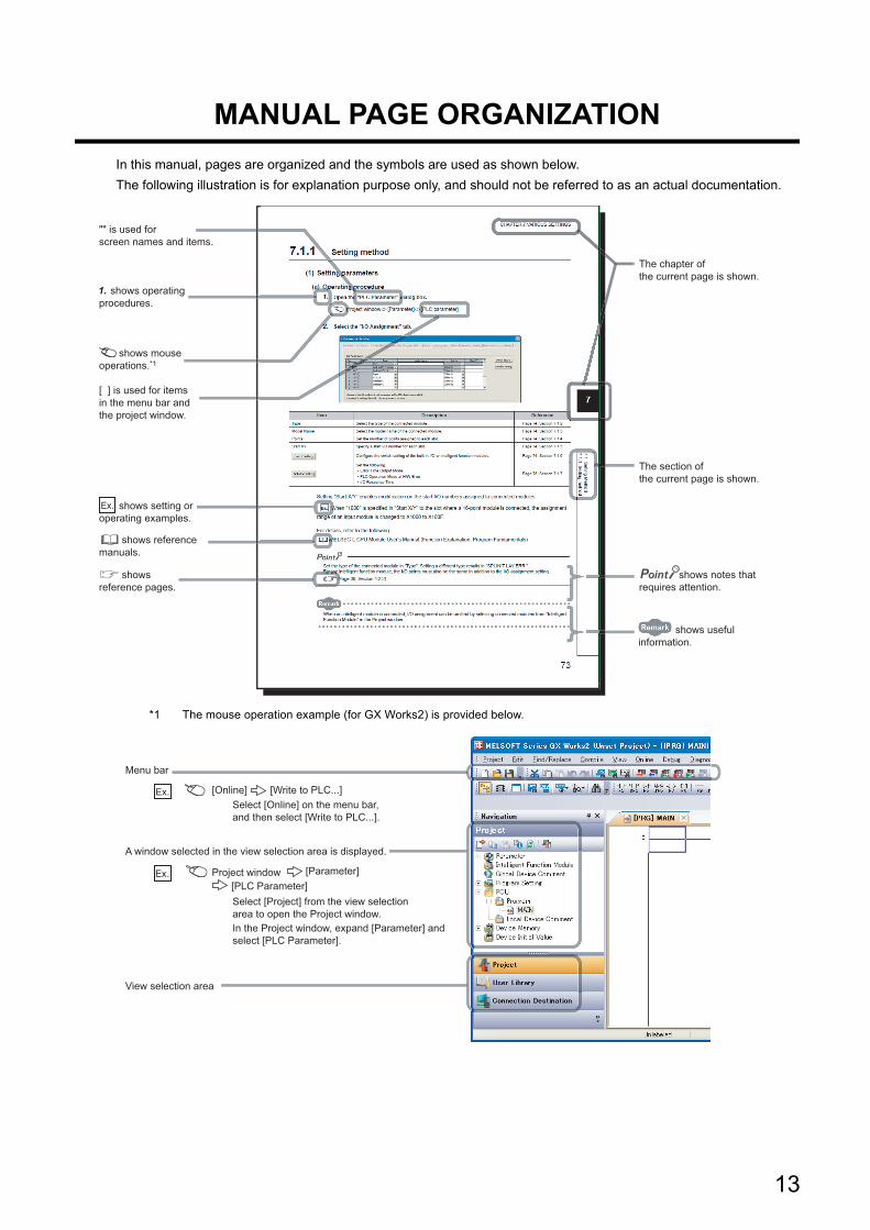
MANUAL PAGE ORGANIZATION
In this manual, pages are organized and the symbols are used as shown below.
The following illustration is for explanation purpose only, and should not be referred to as an actual documentation.
*1 The mouse operation example (for GX Works2) is provided below.
The section of
the current page is shown.
The chapter of
the current page is shown.
"" is used for
screen names and items.
[ ] is used for items
in the menu bar and
the project window.
shows operating
procedures.
shows reference
manuals.
shows notes that
requires attention.
shows mouse
operations.*1
shows
reference pages.
shows setting or
operating examples.
Ex.
shows useful
information.
A window selected in the view selection area is displayed.
View selection area
[Online] [Write to PLC...]
Select [Online] on the menu bar,
and then select [Write to PLC...].
Project window [Parameter]
[PLC Parameter]
Select [Project] from the view selection
area to open the Project window.
Menu bar
Ex.
Ex.
In the Project window, expand [Parameter] and
select [PLC Parameter].
13
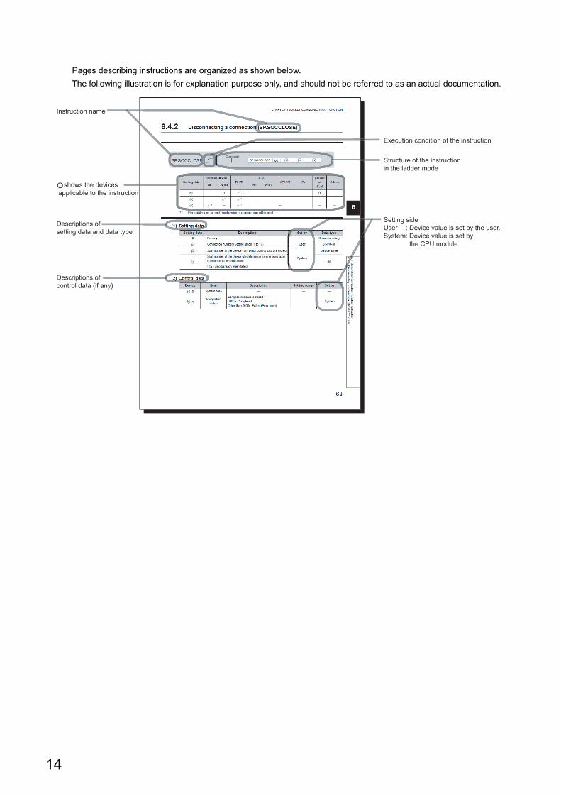
Pages describing instructions are organized as shown below.
The following illustration is for explanation purpose only, and should not be referred to as an actual documentation.
Descriptions of
setting data and data type
Instruction name
Structure of the instruction
in the ladder mode
shows the devices
applicable to the instruction
Descriptions of
control data (if any)
Execution condition of the instruction
Setting side
User : Device value is set by the user.
System: Device value is set by
the CPU module.
14
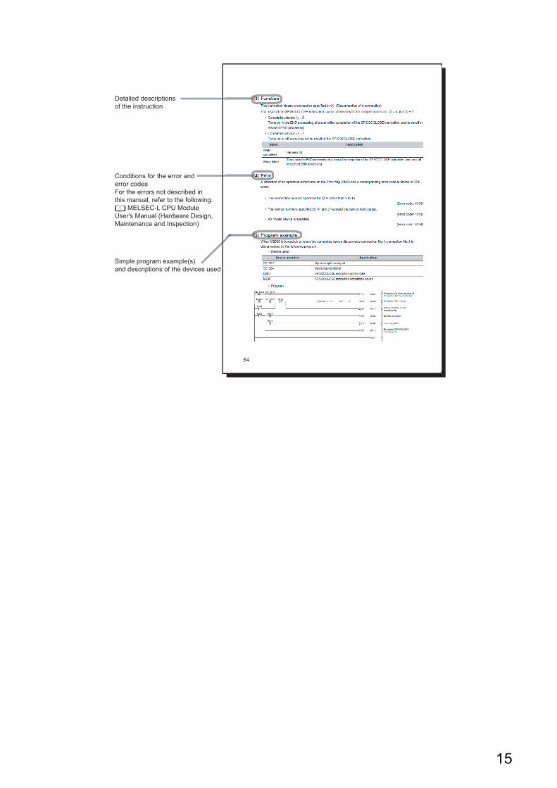
Conditions for the error and
error codes
For the errors not described in
this manual, refer to the following.
MELSEC-L CPU Module
User's Manual (Hardware Design,
Maintenance and Inspection)
Simple program example(s)
and descriptions of the devices used
Detailed descriptions
of the instruction
15
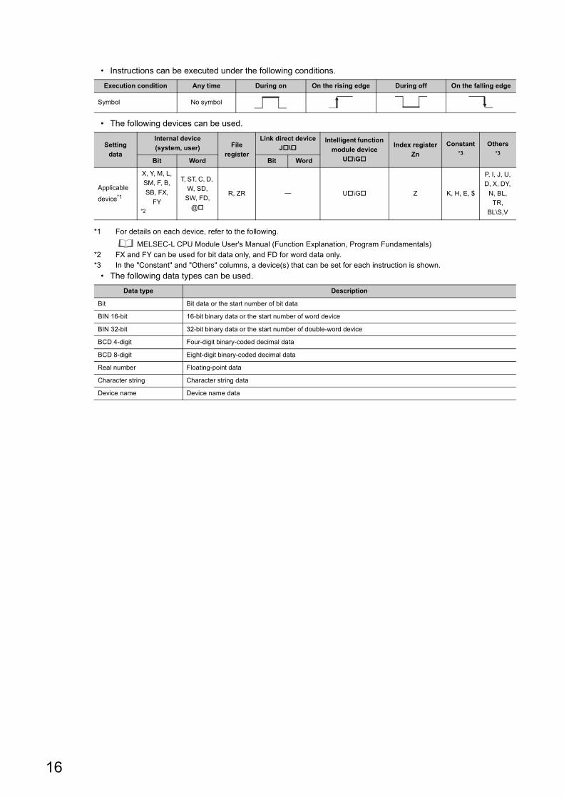
• Instructions can be executed under the following conditions.
• The following devices can be used.
*1 For details on each device, refer to the following.
MELSEC-L CPU Module User's Manual (Function Explanation, Program Fundamentals)*2 FX and FY can be used for bit data only, and FD for word data only.*3 In the "Constant" and "Others" columns, a device(s) that can be set for each instruction is shown.
• The following data types can be used.
Execution condition Any time During on On the rising edge During off On the falling edge
Symbol No symbol
Setting
data
Internal device
(system, user) File
register
Link direct device
J\Intelligent function
module device
U\G
Index register
Zn
Constant*3
Others*3
Bit Word Bit Word
Applicable
device*1
X, Y, M, L,
SM, F, B,
SB, FX,
FY*2
T, ST, C, D,
W, SD,
SW, FD,
@
R, ZR U\G Z K, H, E, $
P, I, J, U,
D, X, DY,
N, BL,
TR,
BL\S,V
Data type Description
Bit Bit data or the start number of bit data
BIN 16-bit 16-bit binary data or the start number of word device
BIN 32-bit 32-bit binary data or the start number of double-word device
BCD 4-digit Four-digit binary-coded decimal data
BCD 8-digit Eight-digit binary-coded decimal data
Real number Floating-point data
Character string Character string data
Device name Device name data
16
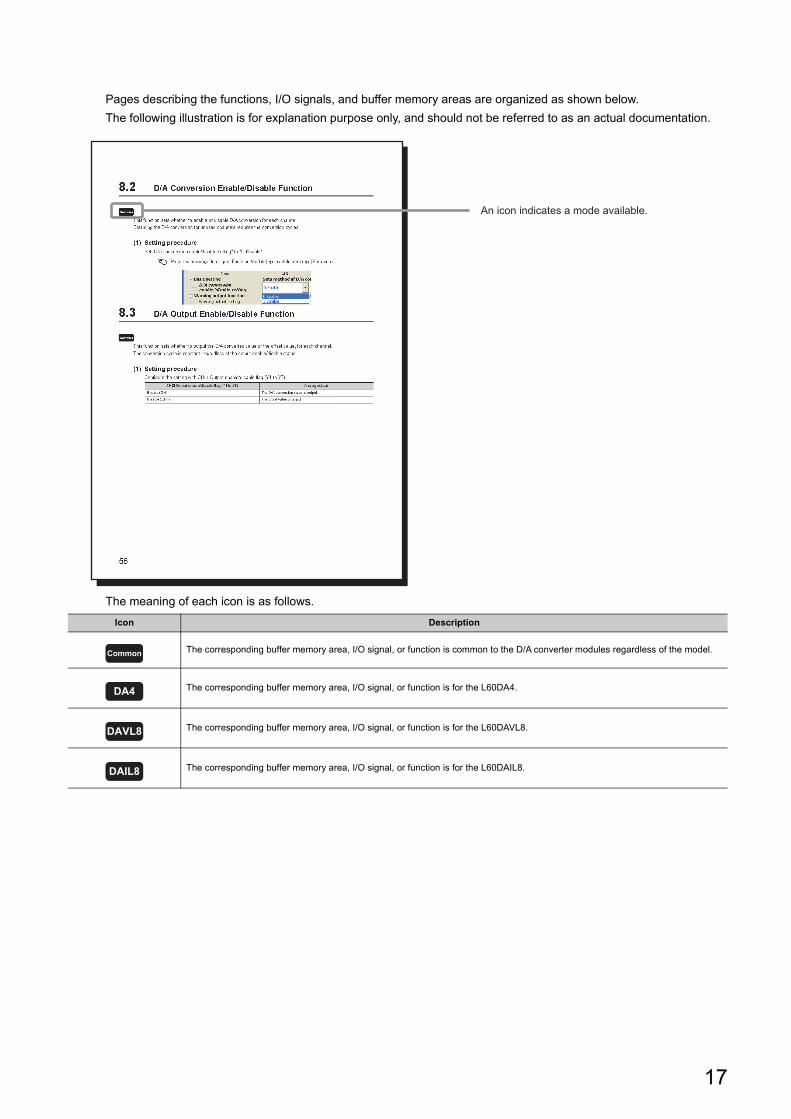
Pages describing the functions, I/O signals, and buffer memory areas are organized as shown below.
The following illustration is for explanation purpose only, and should not be referred to as an actual documentation.
The meaning of each icon is as follows.
Icon Description
The corresponding buffer memory area, I/O signal, or function is common to the D/A converter modules regardless of the model.
The corresponding buffer memory area, I/O signal, or function is for the L60DA4.
The corresponding buffer memory area, I/O signal, or function is for the L60DAVL8.
The corresponding buffer memory area, I/O signal, or function is for the L60DAIL8.
An icon indicates a mode available.
Common
DA4
DAVL8
DAIL8
17
TERMS
Unless otherwise specified, this manual uses the following terms.
PACKING LIST
The following items are included in the package of this product. Before use, check that all the items are included.
Term Description
Buffer memoryA memory in an intelligent function module, where data (such as setting values and monitoring values) exchanged with
a CPU module are stored
D/A converter module A generic term for the L60DA4, L60DAVL8, and L60DAIL8
Display unit A liquid crystal display to be attached to the CPU module
Factory default setting Generic term for analog output ranges of 0 to 5V, 1 to 5V, -10 to 10V, 0 to 20mA, and 4 to 20mA
GX DeveloperThe product name of the software package for the MELSEC programmable controllers
GX Works2
GX Configurator-DA A setting and monitoring tool added in GX Developer (for D/A converter modules)
Head module Abbreviation for the LJ72GF15-T2 CC-Link IE Field Network head module
L60DA4 Abbreviation for the L60DA4 digital-analog converter module
L60DAIL8 Abbreviation for the L60DAIL8 digital-analog converter module
L60DAVL8 Abbreviation for the L60DAVL8 digital-analog converter module
Normal mode"Normal Mode" is the setting value of the drive mode setting in the switch setting.
Note that the normal mode is displayed as "Normal (D/A Converter Processing) Mode" on the programming tool.
Offset/gain setting mode "Offset/Gain Setting Mode" is the setting value of the drive mode setting in the switch setting.
Programming tool A generic term for GX Works2 and GX Developer
Switch settingA generic term for the setting items in the window that is displayed by double-clicking "Switch Setting" of the specified
module on the project window of GX Works2
User range An analog output range where a user can set any values. To use this range, the offset and gain values have to be set.
Watchdog timer errorA D/A converter module monitors its own internal processing by using the watchdog timer. The module generates this
error if the internal processing fails.
D/A converter module
D/A converter module
Before Using the Product
18
CHAPTER 1 D/A CONVERTER MODULE
1
1.1
Ap
plica
tion
CHAPTER 1 D/A CONVERTER MODULE
This chapter describes the application and features of the D/A converter module.
1.1 Application
The D/A converter module converts the digital data received from the CPU module to the analog signal and outputs the
signal to external devices. By converting the data, which has been processed through the CPU module, to an analog
data, the input information can be sent to the devices including an inverter.
The D/A converter module enables works as follows.Connect the module to the control valve to control the flow to a tank. Connect the module to an inverter to control the conveyer belt speed.
Connect the module to the power conditioning equipment to control the heating
temperature of a heater or others.
Digital signal (discrete signal)
Digital to analog
conversionAnalog signal (continuous signal)
Control valveFlow control
Tank
Inverter
Conveyer
Power conditioner
Heater
19
1.2 Features
(1) Features common to the D/A converter module
(a) Scale conversion
This function converts a digital value to the ratio value (%) in any width to represent the digital value in a
numeric value easy to understand.
(b) Error detection and monitoring
When the digital value exceeds the specified range, the module detects an warning so that the digital value
error monitoring and the output control are enabled.
(c) Wave output function
This function outputs any points of the 50000 point wave data (digital value) in analog by executing the D/A
conversion sequentially. The conversion cycle in the wave output function can be set for each channel. A
control with the conversion faster than that of a program control is enabled by the registration of the control
wave data to the D/A converter module and the analog output from the module. And this method is useful for
an analog (torque) control of equipment such as pressing machines and injection molding units. Because the
update of the analog output value of the wave output function is not affected by the scan time of the CPU
module, a faster and smoother analog control is available.
(d) Easy setting with GX Works2
Programming is reduced because the initial setting or auto refresh setting can be configured on the screen. In
addition, setting status and operating status of modules can be checked easily. With the wave output function,
wave data can be created easily by using "Create Wave Output Data".
(2) Features of the L60DA4
(a) Improved response by high-speed conversion
The high-speed conversion speed of 20s/channel is achieved.
(b) Detailed control by high resolution
In all analog output ranges, the high resolution of 1/20000 is achieved.
(c) Reliability by high accuracy
The high accuracy is achieved for the maximum value of analog output value: 0.1% (ambient temperature:
25C) and 0.3% (ambient temperature: 0 to 55).
(3) Features of the L60DAVL8 and L60DAIL8With the same basic functions of the L60DA4, the L60DAVL8 and L60DAIL8 can perform analog output (8
channels), which is two times as much as the L60DA4 per module. With this feature, even in a system where a
large number of analog output points are used, the number of analog output modules can be reduced by using
the L60DAVL8 or L60DAIL8, and thus costs of the system are reduced.
20
CHAPTER 2 PART NAMES
2
CHAPTER 2 PART NAMES
The following table shows the part names of the D/A converter module.
• L60DA4
• L60DAVL8, L60DAIL8
3)
4)
6) 7)
1) 8)
2)1)
1)
5)
1)
3)
4)
6) 7)
1) 8)
2)
1)1)
5)
1)
21
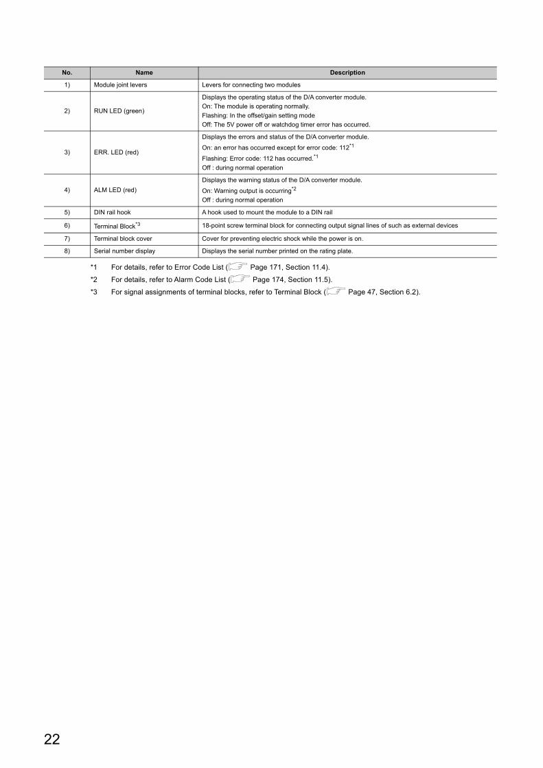
*1 For details, refer to Error Code List ( Page 171, Section 11.4).
*2 For details, refer to Alarm Code List ( Page 174, Section 11.5).
*3 For signal assignments of terminal blocks, refer to Terminal Block ( Page 47, Section 6.2).
No. Name Description
1) Module joint levers Levers for connecting two modules
2) RUN LED (green)
Displays the operating status of the D/A converter module.
On: The module is operating normally.
Flashing: In the offset/gain setting mode
Off: The 5V power off or watchdog timer error has occurred.
3) ERR. LED (red)
Displays the errors and status of the D/A converter module.
On: an error has occurred except for error code: 112*1
Flashing: Error code: 112 has occurred.*1
Off : during normal operation
4) ALM LED (red)
Displays the warning status of the D/A converter module.
On: Warning output is occurring*2
Off : during normal operation
5) DIN rail hook A hook used to mount the module to a DIN rail
6) Terminal Block*3 18-point screw terminal block for connecting output signal lines of such as external devices
7) Terminal block cover Cover for preventing electric shock while the power is on.
8) Serial number display Displays the serial number printed on the rating plate.
22
CHAPTER 3 SPECIFICATIONS
3
3.1
Ge
ne
ral S
pe
cificatio
ns
CHAPTER 3 SPECIFICATIONS
This chapter describes general specifications, performance specifications, function list, list of I/O signals, and list of
buffer memory addresses.
3.1 General Specifications
For the general specifications of the D/A converter module, refer to the following.
"Safety Guidelines", the manual provided with the CPU module or head module
23
3.2 Performance Specifications
The following table shows the performance specifications of the D/A converter module.
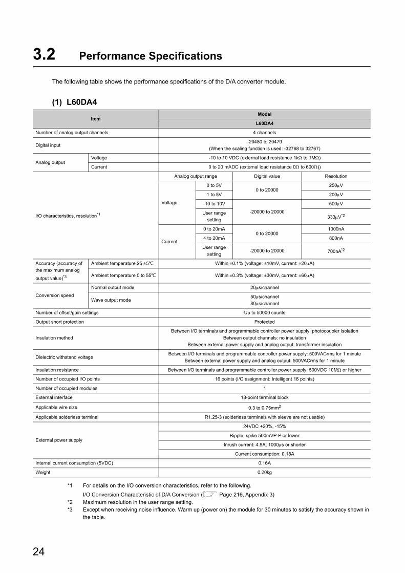
(1) L60DA4
*1 For details on the I/O conversion characteristics, refer to the following.
I/O Conversion Characteristic of D/A Conversion ( Page 216, Appendix 3)*2 Maximum resolution in the user range setting.*3 Except when receiving noise influence. Warm up (power on) the module for 30 minutes to satisfy the accuracy shown in
the table.
ItemModel
L60DA4
Number of analog output channels 4 channels
Digital input-20480 to 20479
(When the scaling function is used: -32768 to 32767)
Analog outputVoltage -10 to 10 VDC (external load resistance 1k to 1M)
Current 0 to 20 mADC (external load resistance 0 to 600))
I/O characteristics, resolution*1
Analog output range Digital value Resolution
Voltage
0 to 5V0 to 20000
250V
1 to 5V 200V
-10 to 10V
-20000 to 20000
500V
User range
setting333V*2
Current
0 to 20mA0 to 20000
1000nA
4 to 20mA 800nA
User range
setting-20000 to 20000 700nA*2
Accuracy (accuracy of
the maximum analog
output value)*3
Ambient temperature 25 5 Within 0.1% (voltage: 10mV, current: 20A)
Ambient temperature 0 to 55 Within 0.3% (voltage: 30mV, current: 60A)
Conversion speed
Normal output mode 20s/channel
Wave output mode50s/channel
80s/channel
Number of offset/gain settings Up to 50000 counts
Output short protection Protected
Insulation method
Between I/O terminals and programmable controller power supply: photocoupler isolation
Between output channels: no insulation
Between external power supply and analog output: transformer insulation
Dielectric withstand voltageBetween I/O terminals and programmable controller power supply: 500VACrms for 1 minute
Between external power supply and analog output: 500VACrms for 1 minute
Insulation resistance Between I/O terminals and programmable controller power supply: 500VDC 10M or higher
Number of occupied I/O points 16 points (I/O assignment: Intelligent 16 points)
Number of occupied modules 1
External interface 18-point terminal block
Applicable wire size 0.3 to 0.75mm2
Applicable solderless terminal R1.25-3 (solderless terminals with sleeve are not usable)
External power supply
24VDC +20%, -15%
Ripple, spike 500mVP-P or lower
Inrush current: 4.9A, 1000s or shorter
Current consumption: 0.18A
Internal current consumption (5VDC) 0.16A
Weight 0.20kg
24
CHAPTER 3 SPECIFICATIONS
3
3.2
Pe
rform
an
ce S
pe
cificatio
ns
(2) L60DAVL8
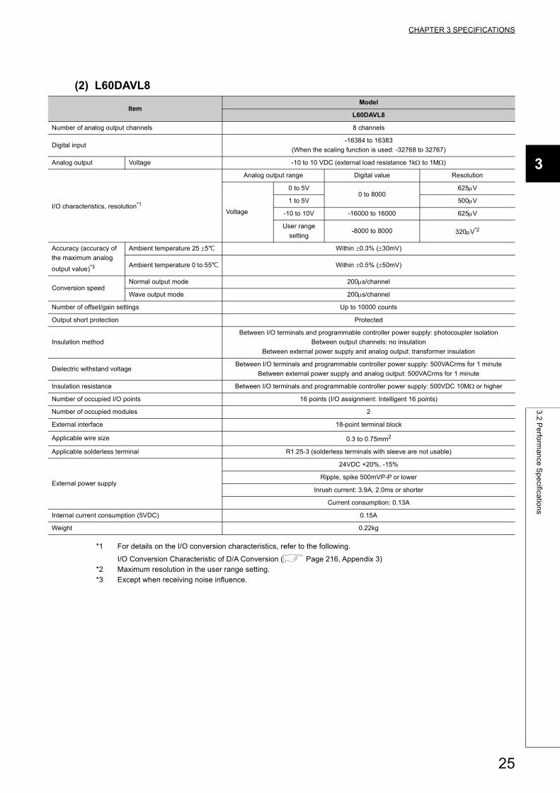
*1 For details on the I/O conversion characteristics, refer to the following.
I/O Conversion Characteristic of D/A Conversion ( Page 216, Appendix 3)*2 Maximum resolution in the user range setting.*3 Except when receiving noise influence.
ItemModel
L60DAVL8
Number of analog output channels 8 channels
Digital input-16384 to 16383
(When the scaling function is used: -32768 to 32767)
Analog output Voltage -10 to 10 VDC (external load resistance 1k to 1M)
I/O characteristics, resolution*1
Analog output range Digital value Resolution
Voltage
0 to 5V0 to 8000
625V
1 to 5V 500V
-10 to 10V -16000 to 16000 625V
User range
setting-8000 to 8000 320V*2
Accuracy (accuracy of
the maximum analog
output value)*3
Ambient temperature 25 5 Within 0.3% (30mV)
Ambient temperature 0 to 55 Within 0.5% (50mV)
Conversion speedNormal output mode 200s/channel
Wave output mode 200s/channel
Number of offset/gain settings Up to 10000 counts
Output short protection Protected
Insulation method
Between I/O terminals and programmable controller power supply: photocoupler isolation
Between output channels: no insulation
Between external power supply and analog output: transformer insulation
Dielectric withstand voltageBetween I/O terminals and programmable controller power supply: 500VACrms for 1 minute
Between external power supply and analog output: 500VACrms for 1 minute
Insulation resistance Between I/O terminals and programmable controller power supply: 500VDC 10M or higher
Number of occupied I/O points 16 points (I/O assignment: Intelligent 16 points)
Number of occupied modules 2
External interface 18-point terminal block
Applicable wire size 0.3 to 0.75mm2
Applicable solderless terminal R1.25-3 (solderless terminals with sleeve are not usable)
External power supply
24VDC +20%, -15%
Ripple, spike 500mVP-P or lower
Inrush current: 3.9A, 2.0ms or shorter
Current consumption: 0.13A
Internal current consumption (5VDC) 0.15A
Weight 0.22kg
25
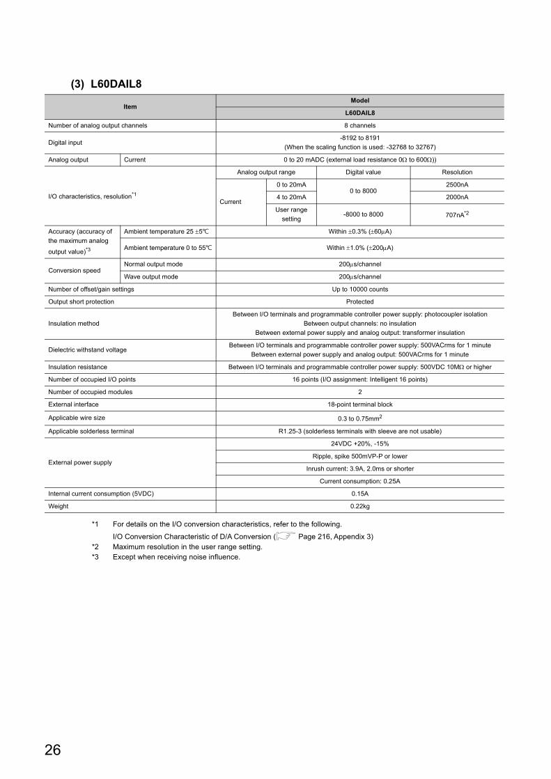
(3) L60DAIL8
*1 For details on the I/O conversion characteristics, refer to the following.
I/O Conversion Characteristic of D/A Conversion ( Page 216, Appendix 3)*2 Maximum resolution in the user range setting.*3 Except when receiving noise influence.
ItemModel
L60DAIL8
Number of analog output channels 8 channels
Digital input-8192 to 8191
(When the scaling function is used: -32768 to 32767)
Analog output Current 0 to 20 mADC (external load resistance 0 to 600))
I/O characteristics, resolution*1
Analog output range Digital value Resolution
Current
0 to 20mA0 to 8000
2500nA
4 to 20mA 2000nA
User range
setting-8000 to 8000 707nA*2
Accuracy (accuracy of
the maximum analog
output value)*3
Ambient temperature 25 5 Within 0.3% (60A)
Ambient temperature 0 to 55 Within 1.0% (200A)
Conversion speedNormal output mode 200s/channel
Wave output mode 200s/channel
Number of offset/gain settings Up to 10000 counts
Output short protection Protected
Insulation method
Between I/O terminals and programmable controller power supply: photocoupler isolation
Between output channels: no insulation
Between external power supply and analog output: transformer insulation
Dielectric withstand voltageBetween I/O terminals and programmable controller power supply: 500VACrms for 1 minute
Between external power supply and analog output: 500VACrms for 1 minute
Insulation resistance Between I/O terminals and programmable controller power supply: 500VDC 10M or higher
Number of occupied I/O points 16 points (I/O assignment: Intelligent 16 points)
Number of occupied modules 2
External interface 18-point terminal block
Applicable wire size 0.3 to 0.75mm2
Applicable solderless terminal R1.25-3 (solderless terminals with sleeve are not usable)
External power supply
24VDC +20%, -15%
Ripple, spike 500mVP-P or lower
Inrush current: 3.9A, 2.0ms or shorter
Current consumption: 0.25A
Internal current consumption (5VDC) 0.15A
Weight 0.22kg
26
CHAPTER 3 SPECIFICATIONS
3
3.2
Pe
rform
an
ce S
pe
cificatio
ns
3.2
.1 N
um
be
r of p
ara
me
ter se
tting
s
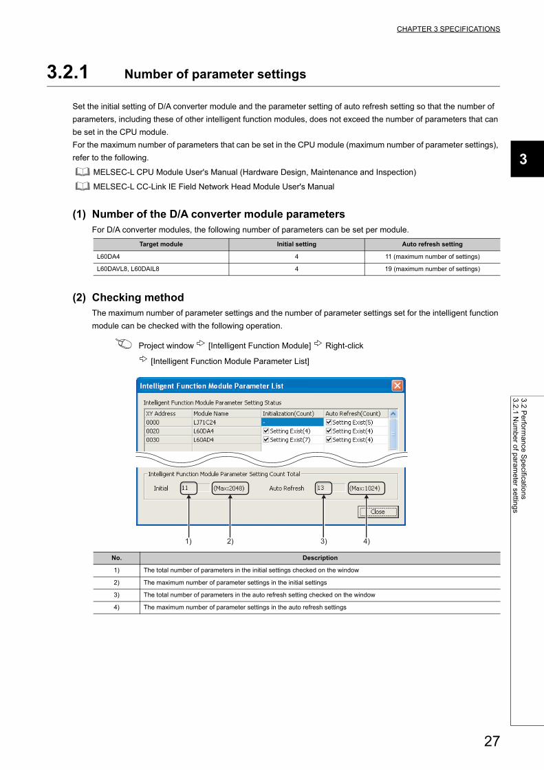
3.2.1 Number of parameter settings
Set the initial setting of D/A converter module and the parameter setting of auto refresh setting so that the number of
parameters, including these of other intelligent function modules, does not exceed the number of parameters that can
be set in the CPU module.
For the maximum number of parameters that can be set in the CPU module (maximum number of parameter settings),
refer to the following.
MELSEC-L CPU Module User's Manual (Hardware Design, Maintenance and Inspection)
MELSEC-L CC-Link IE Field Network Head Module User's Manual
(1) Number of the D/A converter module parametersFor D/A converter modules, the following number of parameters can be set per module.
(2) Checking methodThe maximum number of parameter settings and the number of parameter settings set for the intelligent function
module can be checked with the following operation.
Project window [Intelligent Function Module] Right-click
[Intelligent Function Module Parameter List]
Target module Initial setting Auto refresh setting
L60DA4 4 11 (maximum number of settings)
L60DAVL8, L60DAIL8 4 19 (maximum number of settings)
No. Description
1) The total number of parameters in the initial settings checked on the window
2) The maximum number of parameter settings in the initial settings
3) The total number of parameters in the auto refresh setting checked on the window
4) The maximum number of parameter settings in the auto refresh settings
1) 2) 3) 4)
27
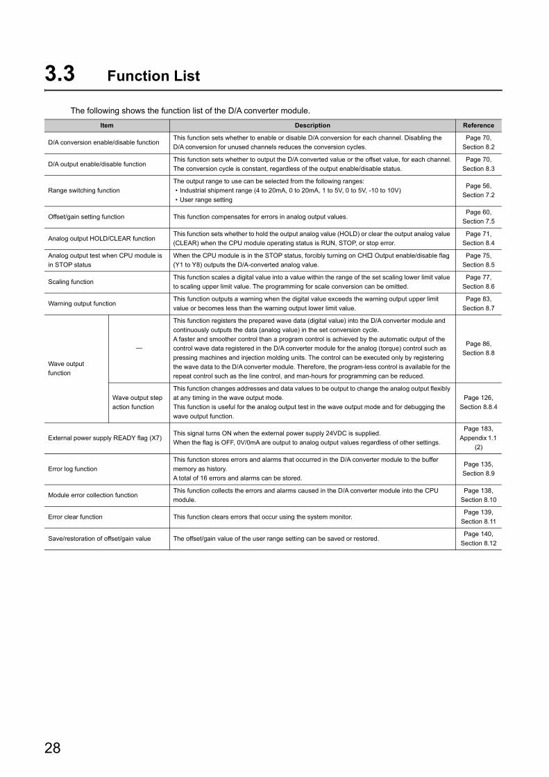
3.3 Function List
The following shows the function list of the D/A converter module.
Item Description Reference
D/A conversion enable/disable functionThis function sets whether to enable or disable D/A conversion for each channel. Disabling the
D/A conversion for unused channels reduces the conversion cycles.
Page 70,
Section 8.2
D/A output enable/disable functionThis function sets whether to output the D/A converted value or the offset value, for each channel.
The conversion cycle is constant, regardless of the output enable/disable status.
Page 70,
Section 8.3
Range switching function
The output range to use can be selected from the following ranges:
• Industrial shipment range (4 to 20mA, 0 to 20mA, 1 to 5V, 0 to 5V, -10 to 10V)
• User range setting
Page 56,
Section 7.2
Offset/gain setting function This function compensates for errors in analog output values.Page 60,
Section 7.5
Analog output HOLD/CLEAR functionThis function sets whether to hold the output analog value (HOLD) or clear the output analog value
(CLEAR) when the CPU module operating status is RUN, STOP, or stop error.
Page 71,
Section 8.4
Analog output test when CPU module is
in STOP status
When the CPU module is in the STOP status, forcibly turning on CH Output enable/disable flag
(Y1 to Y8) outputs the D/A-converted analog value.
Page 75,
Section 8.5
Scaling functionThis function scales a digital value into a value within the range of the set scaling lower limit value
to scaling upper limit value. The programming for scale conversion can be omitted.
Page 77,
Section 8.6
Warning output functionThis function outputs a warning when the digital value exceeds the warning output upper limit
value or becomes less than the warning output lower limit value.
Page 83,
Section 8.7
Wave output
function
This function registers the prepared wave data (digital value) into the D/A converter module and
continuously outputs the data (analog value) in the set conversion cycle.
A faster and smoother control than a program control is achieved by the automatic output of the
control wave data registered in the D/A converter module for the analog (torque) control such as
pressing machines and injection molding units. The control can be executed only by registering
the wave data to the D/A converter module. Therefore, the program-less control is available for the
repeat control such as the line control, and man-hours for programming can be reduced.
Page 86,
Section 8.8
Wave output step
action function
This function changes addresses and data values to be output to change the analog output flexibly
at any timing in the wave output mode.
This function is useful for the analog output test in the wave output mode and for debugging the
wave output function.
Page 126,
Section 8.8.4
External power supply READY flag (X7)This signal turns ON when the external power supply 24VDC is supplied.
When the flag is OFF, 0V/0mA are output to analog output values regardless of other settings.
Page 183,
Appendix 1.1
(2)
Error log function
This function stores errors and alarms that occurred in the D/A converter module to the buffer
memory as history.
A total of 16 errors and alarms can be stored.
Page 135,
Section 8.9
Module error collection functionThis function collects the errors and alarms caused in the D/A converter module into the CPU
module.
Page 138,
Section 8.10
Error clear function This function clears errors that occur using the system monitor.Page 139,
Section 8.11
Save/restoration of offset/gain value The offset/gain value of the user range setting can be saved or restored.Page 140,
Section 8.12
28
CHAPTER 3 SPECIFICATIONS
3
3.4
I/O S
ign
al L
ist
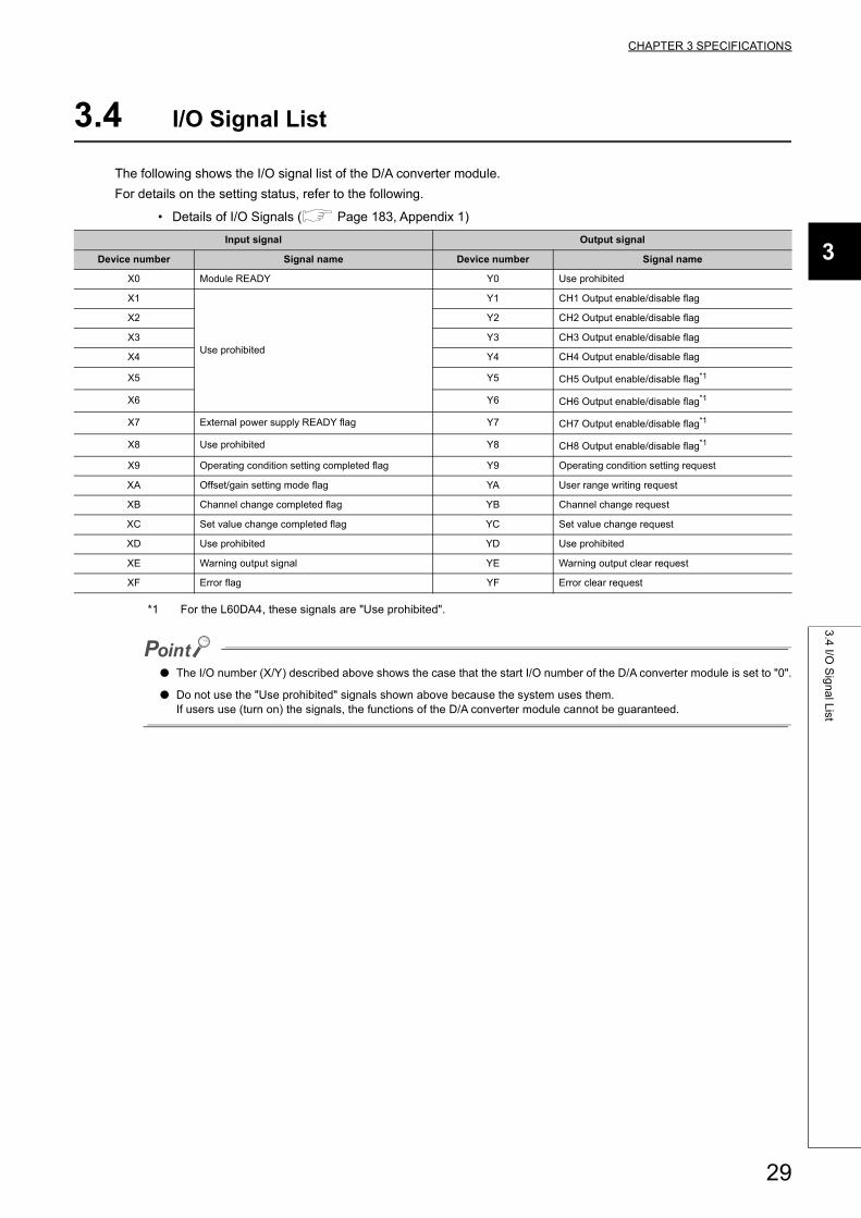
3.4 I/O Signal List
The following shows the I/O signal list of the D/A converter module.
For details on the setting status, refer to the following.
• Details of I/O Signals ( Page 183, Appendix 1)
*1 For the L60DA4, these signals are "Use prohibited".
● The I/O number (X/Y) described above shows the case that the start I/O number of the D/A converter module is set to "0".
● Do not use the "Use prohibited" signals shown above because the system uses them.If users use (turn on) the signals, the functions of the D/A converter module cannot be guaranteed.
Input signal Output signal
Device number Signal name Device number Signal name
X0 Module READY Y0 Use prohibited
X1
Use prohibited
Y1 CH1 Output enable/disable flag
X2 Y2 CH2 Output enable/disable flag
X3 Y3 CH3 Output enable/disable flag
X4 Y4 CH4 Output enable/disable flag
X5 Y5 CH5 Output enable/disable flag*1
X6 Y6 CH6 Output enable/disable flag*1
X7 External power supply READY flag Y7 CH7 Output enable/disable flag*1
X8 Use prohibited Y8 CH8 Output enable/disable flag*1
X9 Operating condition setting completed flag Y9 Operating condition setting request
XA Offset/gain setting mode flag YA User range writing request
XB Channel change completed flag YB Channel change request
XC Set value change completed flag YC Set value change request
XD Use prohibited YD Use prohibited
XE Warning output signal YE Warning output clear request
XF Error flag YF Error clear request
29
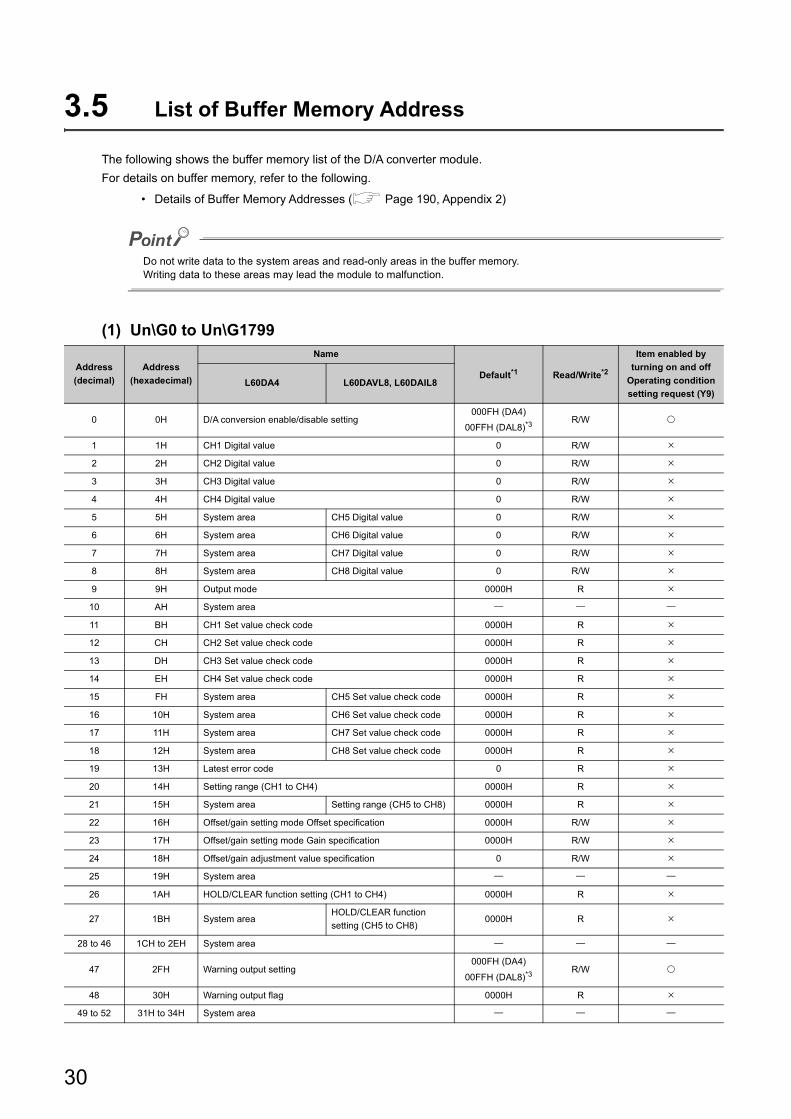
3.5 List of Buffer Memory Address
The following shows the buffer memory list of the D/A converter module.
For details on buffer memory, refer to the following.
• Details of Buffer Memory Addresses ( Page 190, Appendix 2)
Do not write data to the system areas and read-only areas in the buffer memory.Writing data to these areas may lead the module to malfunction.
(1) Un\G0 to Un\G1799
Address
(decimal)
Address
(hexadecimal)
Name
Default*1 Read/Write*2
Item enabled by
turning on and off
Operating condition
setting request (Y9)L60DA4 L60DAVL8, L60DAIL8
0 0H D/A conversion enable/disable setting000FH (DA4)
00FFH (DAL8)*3R/W
1 1H CH1 Digital value 0 R/W
2 2H CH2 Digital value 0 R/W
3 3H CH3 Digital value 0 R/W
4 4H CH4 Digital value 0 R/W
5 5H System area CH5 Digital value 0 R/W
6 6H System area CH6 Digital value 0 R/W
7 7H System area CH7 Digital value 0 R/W
8 8H System area CH8 Digital value 0 R/W
9 9H Output mode 0000H R
10 AH System area
11 BH CH1 Set value check code 0000H R
12 CH CH2 Set value check code 0000H R
13 DH CH3 Set value check code 0000H R
14 EH CH4 Set value check code 0000H R
15 FH System area CH5 Set value check code 0000H R
16 10H System area CH6 Set value check code 0000H R
17 11H System area CH7 Set value check code 0000H R
18 12H System area CH8 Set value check code 0000H R
19 13H Latest error code 0 R
20 14H Setting range (CH1 to CH4) 0000H R
21 15H System area Setting range (CH5 to CH8) 0000H R
22 16H Offset/gain setting mode Offset specification 0000H R/W
23 17H Offset/gain setting mode Gain specification 0000H R/W
24 18H Offset/gain adjustment value specification 0 R/W
25 19H System area
26 1AH HOLD/CLEAR function setting (CH1 to CH4) 0000H R
27 1BH System areaHOLD/CLEAR function
setting (CH5 to CH8)0000H R
28 to 46 1CH to 2EH System area
47 2FH Warning output setting000FH (DA4)
00FFH (DAL8)*3R/W
48 30H Warning output flag 0000H R
49 to 52 31H to 34H System area
30
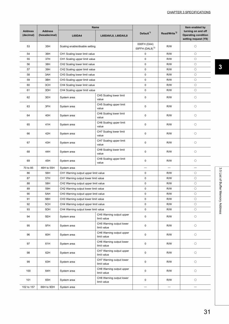
CHAPTER 3 SPECIFICATIONS
3
3.5
List o
f Bu
ffer M
em
ory A
dd
ress
53 35H Scaling enable/disable setting000FH (DA4)
00FFH (DAL8)*3R/W
54 36H CH1 Scaling lower limit value 0 R/W
55 37H CH1 Scaling upper limit value 0 R/W
56 38H CH2 Scaling lower limit value 0 R/W
57 39H CH2 Scaling upper limit value 0 R/W
58 3AH CH3 Scaling lower limit value 0 R/W
59 3BH CH3 Scaling upper limit value 0 R/W
60 3CH CH4 Scaling lower limit value 0 R/W
61 3DH CH4 Scaling upper limit value 0 R/W
62 3EH System areaCH5 Scaling lower limit
value0 R/W
63 3FH System areaCH5 Scaling upper limit
value0 R/W
64 40H System areaCH6 Scaling lower limit
value0 R/W
65 41H System areaCH6 Scaling upper limit
value0 R/W
66 42H System areaCH7 Scaling lower limit
value0 R/W
67 43H System areaCH7 Scaling upper limit
value0 R/W
68 44H System areaCH8 Scaling lower limit
value0 R/W
69 45H System areaCH8 Scaling upper limit
value0 R/W
70 to 85 46H to 55H System area
86 56H CH1 Warning output upper limit value 0 R/W
87 57H CH1 Warning output lower limit value 0 R/W
88 58H CH2 Warning output upper limit value 0 R/W
89 59H CH2 Warning output lower limit value 0 R/W
90 5AH CH3 Warning output upper limit value 0 R/W
91 5BH CH3 Warning output lower limit value 0 R/W
92 5CH CH4 Warning output upper limit value 0 R/W
93 5DH CH4 Warning output lower limit value 0 R/W
94 5EH System areaCH5 Warning output upper
limit value0 R/W
95 5FH System areaCH5 Warning output lower
limit value0 R/W
96 60H System areaCH6 Warning output upper
limit value0 R/W
97 61H System areaCH6 Warning output lower
limit value0 R/W
98 62H System areaCH7 Warning output upper
limit value0 R/W
99 63H System areaCH7 Warning output lower
limit value0 R/W
100 64H System areaCH8 Warning output upper
limit value0 R/W
101 65H System areaCH8 Warning output lower
limit value0 R/W
102 to 157 66H to 9DH System area
Address
(decimal)
Address
(hexadecimal)
Name
Default*1 Read/Write*2
Item enabled by
turning on and off
Operating condition
setting request (Y9)L60DA4 L60DAVL8, L60DAIL8
31
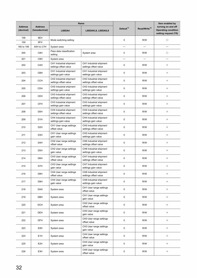
158 9EHMode switching setting 0 R/W
159 9FH
160 to 199 A0H to C7H System area
200 C8HPass data classification
settingSystem area 0 R/W
201 C9H System area
202 CAHCH1 Industrial shipment
settings offset value
CH1 Industrial shipment
settings offset value0 R/W
203 CBHCH1 Industrial shipment
settings gain value
CH1 Industrial shipment
settings gain value0 R/W
204 CCHCH2 Industrial shipment
settings offset value
CH2 Industrial shipment
settings offset value0 R/W
205 CDHCH2 Industrial shipment
settings gain value
CH2 Industrial shipment
settings gain value0 R/W
206 CEHCH3 Industrial shipment
settings offset value
CH3 Industrial shipment
settings offset value0 R/W
207 CFHCH3 Industrial shipment
settings gain value
CH3 Industrial shipment
settings gain value0 R/W
208 D0HCH4 Industrial shipment
settings offset value
CH4 Industrial shipment
settings offset value0 R/W
209 D1HCH4 Industrial shipment
settings gain value
CH4 Industrial shipment
settings gain value0 R/W
210 D2HCH1 User range settings
offset value
CH5 Industrial shipment
settings offset value0 R/W
211 D3HCH1 User range settings
gain value
CH5 Industrial shipment
settings gain value0 R/W
212 D4HCH2 User range settings
offset value
CH6 Industrial shipment
settings offset value0 R/W
213 D5HCH2 User range settings
gain value
CH6 Industrial shipment
settings gain value0 R/W
214 D6HCH3 User range settings
offset value
CH7 Industrial shipment
settings offset value0 R/W
215 D7HCH3 User range settings
gain value
CH7 Industrial shipment
settings gain value0 R/W
216 D8HCH4 User range settings
offset value
CH8 Industrial shipment
settings offset value0 R/W
217 D9HCH4 User range settings
gain value
CH8 Industrial shipment
settings gain value0 R/W
218 DAH System areaCH1 User range settings
offset value0 R/W
219 DBH System areaCH1 User range settings
gain value0 R/W
220 DCH System areaCH2 User range settings
offset value0 R/W
221 DEH System areaCH2 User range settings
gain value0 R/W
222 DFH System areaCH3 User range settings
offset value0 R/W
223 E0H System areaCH3 User range settings
gain value0 R/W
224 E1H System areaCH4 User range settings
offset value0 R/W
225 E2H System areaCH4 User range settings
gain value0 R/W
226 E3H System areaCH5 User range settings
offset value0 R/W
Address
(decimal)
Address
(hexadecimal)
Name
Default*1 Read/Write*2
Item enabled by
turning on and off
Operating condition
setting request (Y9)L60DA4 L60DAVL8, L60DAIL8
32
CHAPTER 3 SPECIFICATIONS
3
3.5
List o
f Bu
ffer M
em
ory A
dd
ress
227 E4H System areaCH5 User range settings
gain value0 R/W
228 E5H System areaCH6 User range settings
offset value0 R/W
229 E6H System areaCH6 User range settings
gain value0 R/W
230 E7H System areaCH7 User range settings
offset value0 R/W
231 E8H System areaCH7 User range settings
gain value0 R/W
232 E9H System areaCH8 User range settings
offset value0 R/W
233 EAH System areaCH8 User range settings
gain value0 R/W
234 to 999 EBH to 3E7H System area
1000 3E8H CH1 Wave output start/stop request 0 R/W
1001 3E9H CH2 Wave output start/stop request 0 R/W
1002 3EAH CH3 Wave output start/stop request 0 R/W
1003 3EBH CH4 Wave output start/stop request 0 R/W
1004 3ECH System areaCH5 Wave output start/stop
request0 R/W
1005 3EDH System areaCH6 Wave output start/stop
request0 R/W
1006 3EEH System areaCH7 Wave output start/stop
request0 R/W
1007 3EFH System areaCH8 Wave output start/stop
request0 R/W
1008 3F0H CH1 Output setting during wave output stop 1 R/W
1009 3F1H CH2 Output setting during wave output stop 1 R/W
1010 3F2H CH3 Output setting during wave output stop 1 R/W
1011 3F3H CH4 Output setting during wave output stop 1 R/W
1012 3F4H System areaCH5 Output setting during
wave output stop1 R/W
1013 3F5H System areaCH6 Output setting during
wave output stop1 R/W
1014 3F6H System areaCH7 Output setting during
wave output stop1 R/W
1015 3F7H System areaCH8 Output setting during
wave output stop1 R/W
1016 3F8H CH1 Output value during wave output stop 0 R/W
1017 3F9H CH2 Output value during wave output stop 0 R/W
1018 3FAH CH3 Output value during wave output stop 0 R/W
1019 3FBH CH4 Output value during wave output stop 0 R/W
1020 3FCH System areaCH5 Output value during
wave output stop0 R/W
1021 3FDH System areaCH6 Output value during
wave output stop0 R/W
1022 3FEH System areaCH7 Output value during
wave output stop0 R/W
1023 3FFH System areaCH8 Output value during
wave output stop0 R/W
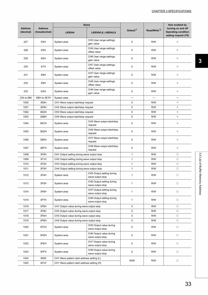
1024 400H CH1 Wave pattern start address setting (L)5000 R/W
1025 401H CH1 Wave pattern start address setting (H)
Address
(decimal)
Address
(hexadecimal)
Name
Default*1 Read/Write*2
Item enabled by
turning on and off
Operating condition
setting request (Y9)L60DA4 L60DAVL8, L60DAIL8
33
1026 402H CH2 Wave pattern start address setting (L)5000 R/W
1027 403H CH2 Wave pattern start address setting (H)
1028 404H CH3 Wave pattern start address setting (L)5000 R/W
1029 405H CH3 Wave pattern start address setting (H)
1030 406H CH4 Wave pattern start address setting (L)5000 R/W
1031 407H CH4 Wave pattern start address setting (H)
1032 408H System areaCH5 Wave pattern start
address setting (L)5000 R/W
1033 409H System areaCH5 Wave pattern start
address setting (H)
1034 40AH System areaCH6 Wave pattern start
address setting (L)5000 R/W
1035 40BH System areaCH6 Wave pattern start
address setting (H)
1036 40CH System areaCH7 Wave pattern start
address setting (L)5000 R/W
1037 40DH System areaCH7 Wave pattern start
address setting (H)
1038 40EH System areaCH8 Wave pattern start
address setting (L)5000 R/W
1039 40FH System areaCH8 Wave pattern start
address setting (H)
1040 410H CH1 Wave pattern data points setting (L)0 R/W
1041 411H CH1 Wave pattern data points setting (H)
1042 412H CH2 Wave pattern data points setting (L)0 R/W
1043 413H CH2 Wave pattern data points setting (H)
1044 414H CH3 Wave pattern data points setting (L)0 R/W
1045 415H CH3 Wave pattern data points setting (H)
1046 416H CH4 Wave pattern data points setting (L)0 R/W
1047 417H CH4 Wave pattern data points setting (H)
1048 418H System areaCH5 Wave pattern data
points setting (L)0 R/W
1049 419H System areaCH5 Wave pattern data
points setting (H)
1050 41AH System areaCH6 Wave pattern data
points setting (L)0 R/W
1051 41BH System areaCH6 Wave pattern data
points setting (H)
1052 41CH System areaCH7 Wave pattern data
points setting (L)0 R/W
1053 41DH System areaCH7 Wave pattern data
points setting (H)
1054 41EH System areaCH8 Wave pattern data
points setting (L)0 R/W
1055 41FH System areaCH8 Wave pattern data
points setting (H)
1056 420H CH1 Wave pattern output repetition setting 1 R/W
1057 421H CH2 Wave pattern output repetition setting 1 R/W
1058 422H CH3 Wave pattern output repetition setting 1 R/W
1059 423H CH4 Wave pattern output repetition setting 1 R/W
1060 424H System areaCH5 Wave pattern output
repetition setting1 R/W
1061 425H System areaCH6 Wave pattern output
repetition setting1 R/W
Address
(decimal)
Address
(hexadecimal)
Name
Default*1 Read/Write*2
Item enabled by
turning on and off
Operating condition
setting request (Y9)L60DA4 L60DAVL8, L60DAIL8
34
CHAPTER 3 SPECIFICATIONS
3
3.5
List o
f Bu
ffer M
em
ory A
dd
ress
1062 426H System areaCH7 Wave pattern output
repetition setting1 R/W
1063 427H System areaCH8 Wave pattern output
repetition setting1 R/W
1064 428H CH1 Constant for wave output conversion cycle 1 R/W
1065 429H CH2 Constant for wave output conversion cycle 1 R/W
1066 42AH CH3 Constant for wave output conversion cycle 1 R/W
1067 42BH CH4 Constant for wave output conversion cycle 1 R/W
1068 42CH System areaCH5 Constant for wave
output conversion cycle1 R/W
1069 42DH System areaCH6 Constant for wave
output conversion cycle1 R/W
1070 42EH System areaCH7 Constant for wave
output conversion cycle1 R/W
1071 42FH System areaCH8 Constant for wave
output conversion cycle1 R/W
1072 430H Step action wave output request 0 R/W
1073 to
1079431H to 437H System area
1080 438H CH1 Wave output step action movement amount 0 R/W
1081 439H CH2 Wave output step action movement amount 0 R/W
1082 43AH CH3 Wave output step action movement amount 0 R/W
1083 43BH CH4 Wave output step action movement amount 0 R/W
1084 43CH System areaCH5 Wave output step
action movement amount0 R/W
1085 43DH System areaCH6 Wave output step
action movement amount0 R/W
1086 43EH System areaCH7 Wave output step
action movement amount0 R/W
1087 43FH System areaCH8 Wave output step
action movement amount0 R/W
1088 to
1099440H to 44BH System area
1100 44CH CH1 Wave output status monitor 0 R
1101 44DH CH2 Wave output status monitor 0 R
1102 44EH CH3 Wave output status monitor 0 R
1103 44FH CH4 Wave output status monitor 0 R
1104 450H System areaCH5 Wave output status
monitor0 R
1105 451H System areaCH6 Wave output status
monitor0 R
1106 452H System areaCH7 Wave output status
monitor0 R
1107 453H System areaCH8 Wave output status
monitor0 R
1108 454H CH1 Wave output conversion cycle monitor (L)0 R
1109 455H CH1 Wave output conversion cycle monitor (H)
1110 456H CH2 Wave output conversion cycle monitor (L)0 R
1111 457H CH2 Wave output conversion cycle monitor (H)
1112 458H CH3 Wave output conversion cycle monitor (L)0 R
1113 459H CH3 Wave output conversion cycle monitor (H)
1114 45AH CH4 Wave output conversion cycle monitor (L)0 R
1115 45BH CH4 Wave output conversion cycle monitor (H)
Address
(decimal)
Address
(hexadecimal)
Name
Default*1 Read/Write*2
Item enabled by
turning on and off
Operating condition
setting request (Y9)L60DA4 L60DAVL8, L60DAIL8
35
1116 45CH System areaCH5 Wave output
conversion cycle monitor (L)0 R
1117 45DH System areaCH5 Wave output
conversion cycle monitor (H)
1118 45EH System areaCH6 Wave output
conversion cycle monitor (L)0 R
1119 45FH System areaCH6 Wave output
conversion cycle monitor (H)
1120 460H System areaCH7 Wave output
conversion cycle monitor (L)0 R
1121 461H System areaCH7 Wave output
conversion cycle monitor (H)
1122 462H System areaCH8 Wave output
conversion cycle monitor (L)0 R
1123 463H System areaCH8 Wave output
conversion cycle monitor (H)
1124 464H CH1 Wave pattern output count monitor 0 R
1125 465H CH2 Wave pattern output count monitor 0 R
1126 466H CH3 Wave pattern output count monitor 0 R
1127 467H CH4 Wave pattern output count monitor 0 R
1128 468H System areaCH5 Wave pattern output
count monitor0 R
1129 469H System areaCH6 Wave pattern output
count monitor0 R
1130 46AH System areaCH7 Wave pattern output
count monitor0 R
1131 46BH System areaCH8 Wave pattern output
count monitor0 R
1132 46CH CH1 Wave output current address monitor (L)0 R
1133 46DH CH1 Wave output current address monitor (H)
1134 46EH CH2 Wave output current address monitor (L)0 R
1135 46FH CH2 Wave output current address monitor (H)
1136 470H CH3 Wave output current address monitor (L)0 R
1137 471H CH3 Wave output current address monitor (H)
1138 472H CH4 Wave output current address monitor (L)0 R
1139 473H CH4 Wave output current address monitor (H)
1140 474H System areaCH5 Wave output current
address monitor (L)0 R
1141 475H System areaCH5 Wave output current
address monitor (H)
1142 476H System areaCH6 Wave output current
address monitor (L)0 R
1143 477H System areaCH6 Wave output current
address monitor (H)
1144 478H System areaCH7 Wave output current
address monitor (L)0 R
1145 479H System areaCH7 Wave output current
address monitor (H)
1146 47AH System areaCH8 Wave output current
address monitor (L)0 R
1147 47BH System areaCH8 Wave output current
address monitor (H)
1148 47CH CH1 Wave output current digital value monitor 0 R
1149 47DH CH2 Wave output current digital value monitor 0 R
Address
(decimal)
Address
(hexadecimal)
Name
Default*1 Read/Write*2
Item enabled by
turning on and off
Operating condition
setting request (Y9)L60DA4 L60DAVL8, L60DAIL8
36
CHAPTER 3 SPECIFICATIONS
3
3.5
List o
f Bu
ffer M
em
ory A
dd
ress
1150 47EH CH3 Wave output current digital value monitor 0 R
1151 47FH CH4 Wave output current digital value monitor 0 R
1152 480H System areaCH5 Wave output current
digital value monitor0 R
1153 481H System areaCH6 Wave output current
digital value monitor0 R
1154 482H System areaCH7 Wave output current
digital value monitor0 R
1155 483H System areaCH8 Wave output current
digital value monitor0 R
1156 484HCH1 Wave output digital value outside the range Address
monitor (L)0 R
1157 485HCH1 Wave output digital value outside the range Address
monitor (H)
1158 486HCH2 Wave output digital value outside the range Address
monitor (L)0 R
1159 487HCH2 Wave output digital value outside the range Address
monitor (H)
1160 488HCH3 Wave output digital value outside the range Address
monitor (L)0 R
1161 489HCH3 Wave output digital value outside the range Address
monitor (H)
1162 48AHCH4 Wave output digital value outside the range Address
monitor (L)0 R
1163 48BHCH4 Wave output digital value outside the range Address
monitor (H)
1164 48CH System area
CH5 Wave output digital
value outside the range
Address monitor (L)0 R
1165 48DH System area
CH5 Wave output digital
value outside the range
Address monitor (H)
1166 48EH System area
CH6 Wave output digital
value outside the range
Address monitor (L)0 R
1167 48FH System area
CH6 Wave output digital
value outside the range
Address monitor (H)
1168 490H System area
CH7 Wave output digital
value outside the range
Address monitor (L)0 R
1169 491H System area
CH7 Wave output digital
value outside the range
Address monitor (H)
1170 492H System area
CH8 Wave output digital
value outside the range
Address monitor (L)0 R
1171 493H System area
CH8 Wave output digital
value outside the range
Address monitor (H)
1172 494H CH1 Wave output warning Address monitor (L)0 R
1173 495H CH1 Wave output warning Address monitor (H)
1174 496H CH2 Wave output warning Address monitor (L)0 R
1175 497H CH2 Wave output warning Address monitor (H)
1176 498H CH3 Wave output warning Address monitor (L)0 R
1177 499H CH3 Wave output warning Address monitor (H)
Address
(decimal)
Address
(hexadecimal)
Name
Default*1 Read/Write*2
Item enabled by
turning on and off
Operating condition
setting request (Y9)L60DA4 L60DAVL8, L60DAIL8
37
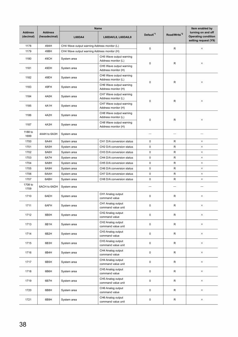
1178 49AH CH4 Wave output warning Address monitor (L)0 R
1179 49BH CH4 Wave output warning Address monitor (H)
1180 49CH System areaCH5 Wave output warning
Address monitor (L)0 R
1181 49DH System areaCH5 Wave output warning
Address monitor (H)
1182 49EH System areaCH6 Wave output warning
Address monitor (L)0 R
1183 49FH System areaCH6 Wave output warning
Address monitor (H)
1184 4A0H System areaCH7 Wave output warning
Address monitor (L)0 R
1185 4A1H System areaCH7 Wave output warning
Address monitor (H)
1186 4A2H System areaCH8 Wave output warning
Address monitor (L)0 R
1187 4A3H System areaCH8 Wave output warning
Address monitor (H)
1188 to
16994A4H to 6A3H System area
1700 6A4H System area CH1 D/A conversion status 0 R
1701 6A5H System area CH2 D/A conversion status 0 R
1702 6A6H System area CH3 D/A conversion status 0 R
1703 6A7H System area CH4 D/A conversion status 0 R
1704 6A8H System area CH5 D/A conversion status 0 R
1705 6A9H System area CH6 D/A conversion status 0 R
1706 6AAH System area CH7 D/A conversion status 0 R
1707 6ABH System area CH8 D/A conversion status 0 R
1708 to
17096ACH to 6ADH System area
1710 6AEH System areaCH1 Analog output
command value0 R
1711 6AFH System areaCH1 Analog output
command value unit0 R
1712 6B0H System areaCH2 Analog output
command value0 R
1713 6B1H System areaCH2 Analog output
command value unit0 R
1714 6B2H System areaCH3 Analog output
command value0 R
1715 6B3H System areaCH3 Analog output
command value unit0 R
1716 6B4H System areaCH4 Analog output
command value0 R
1717 6B5H System areaCH4 Analog output
command value unit0 R
1718 6B6H System areaCH5 Analog output
command value0 R
1719 6B7H System areaCH5 Analog output
command value unit0 R
1720 6B8H System areaCH6 Analog output
command value0 R
1721 6B9H System areaCH6 Analog output
command value unit0 R
Address
(decimal)
Address
(hexadecimal)
Name
Default*1 Read/Write*2
Item enabled by
turning on and off
Operating condition
setting request (Y9)L60DA4 L60DAVL8, L60DAIL8
38
CHAPTER 3 SPECIFICATIONS
3
3.5
List o
f Bu
ffer M
em
ory A
dd
ress
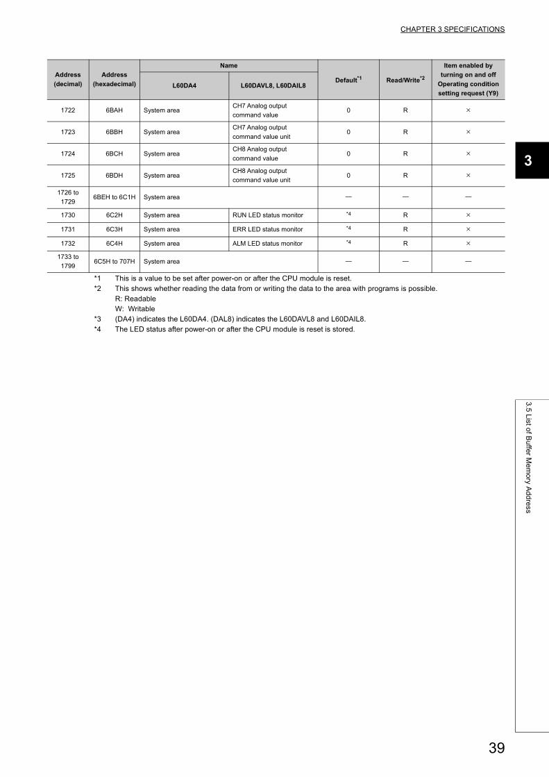
*1 This is a value to be set after power-on or after the CPU module is reset.*2 This shows whether reading the data from or writing the data to the area with programs is possible.
R: ReadableW: Writable
*3 (DA4) indicates the L60DA4. (DAL8) indicates the L60DAVL8 and L60DAIL8.*4 The LED status after power-on or after the CPU module is reset is stored.
1722 6BAH System areaCH7 Analog output
command value0 R
1723 6BBH System areaCH7 Analog output
command value unit0 R
1724 6BCH System areaCH8 Analog output
command value0 R
1725 6BDH System areaCH8 Analog output
command value unit0 R
1726 to
17296BEH to 6C1H System area
1730 6C2H System area RUN LED status monitor *4 R
1731 6C3H System area ERR LED status monitor *4 R
1732 6C4H System area ALM LED status monitor *4 R
1733 to
17996C5H to 707H System area
Address
(decimal)
Address
(hexadecimal)
Name
Default*1 Read/Write*2
Item enabled by
turning on and off
Operating condition
setting request (Y9)L60DA4 L60DAVL8, L60DAIL8
39
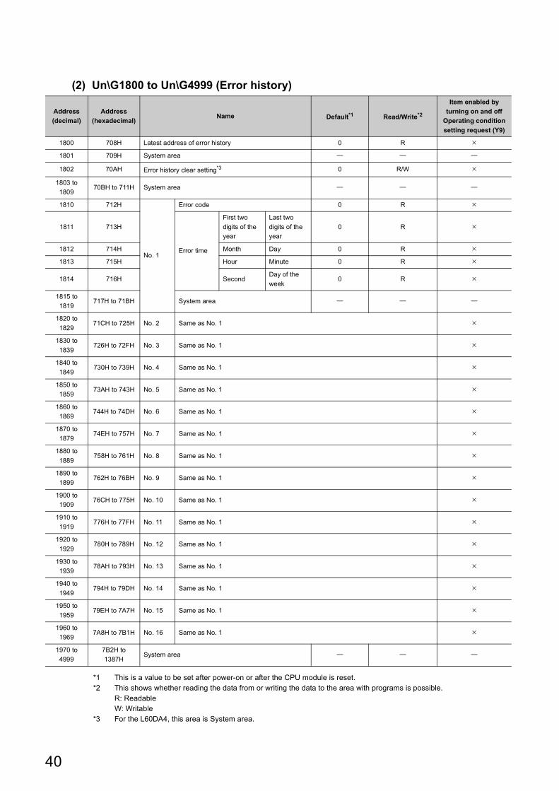
(2) Un\G1800 to Un\G4999 (Error history)
*1 This is a value to be set after power-on or after the CPU module is reset.*2 This shows whether reading the data from or writing the data to the area with programs is possible.
R: ReadableW: Writable
*3 For the L60DA4, this area is System area.
Address
(decimal)
Address
(hexadecimal)Name Default*1 Read/Write*2
Item enabled by
turning on and off
Operating condition
setting request (Y9)
1800 708H Latest address of error history 0 R
1801 709H System area
1802 70AH Error history clear setting*3 0 R/W
1803 to
180970BH to 711H System area
1810 712H
No. 1
Error code 0 R
1811 713H
Error time
First two
digits of the
year
Last two
digits of the
year
0 R
1812 714H Month Day 0 R
1813 715H Hour Minute 0 R
1814 716H SecondDay of the
week0 R
1815 to
1819717H to 71BH System area
1820 to
182971CH to 725H No. 2 Same as No. 1
1830 to
1839726H to 72FH No. 3 Same as No. 1
1840 to
1849730H to 739H No. 4 Same as No. 1
1850 to
185973AH to 743H No. 5 Same as No. 1
1860 to
1869744H to 74DH No. 6 Same as No. 1
1870 to
187974EH to 757H No. 7 Same as No. 1
1880 to
1889758H to 761H No. 8 Same as No. 1
1890 to
1899762H to 76BH No. 9 Same as No. 1
1900 to
190976CH to 775H No. 10 Same as No. 1
1910 to
1919776H to 77FH No. 11 Same as No. 1
1920 to
1929780H to 789H No. 12 Same as No. 1
1930 to
193978AH to 793H No. 13 Same as No. 1
1940 to
1949794H to 79DH No. 14 Same as No. 1
1950 to
195979EH to 7A7H No. 15 Same as No. 1
1960 to
19697A8H to 7B1H No. 16 Same as No. 1
1970 to
4999
7B2H to
1387HSystem area
40
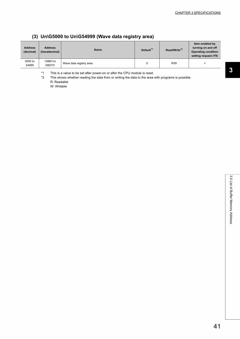
CHAPTER 3 SPECIFICATIONS
3
3.5
List o
f Bu
ffer M
em
ory A
dd
ress
(3) Un\G5000 to Un\G54999 (Wave data registry area)
*1 This is a value to be set after power-on or after the CPU module is reset.*2 This shows whether reading the data from or writing the data to the area with programs is possible.
R: ReadableW: Writable
Address
(decimal)
Address
(hexadecimal)Name Default*1 Read/Write*2
Item enabled by
turning on and off
Operating condition
setting request (Y9)
5000 to
54999
1388H to
D6D7HWave data registry area 0 R/W
41
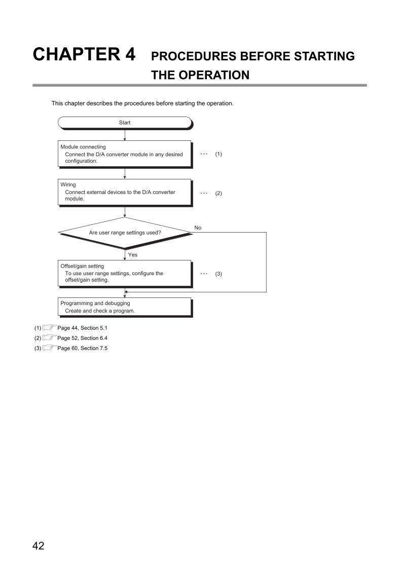
CHAPTER 4 PROCEDURES BEFORE STARTING
THE OPERATION
This chapter describes the procedures before starting the operation.
(1) Page 44, Section 5.1
(2) Page 52, Section 6.4
(3) Page 60, Section 7.5
Start
Module connectingConnect the D/A converter module in any desired configuration.
Yes
No
To use user range settings, configure theoffset/gain setting.
Are user range settings used?
Offset/gain setting
WiringConnect external devices to the D/A convertermodule.
Programming and debuggingCreate and check a program.
(1)
(2)
(3)
42
CHAPTER 4 PROCEDURES BEFORE STARTING THE OPERATION
4
Memo
43
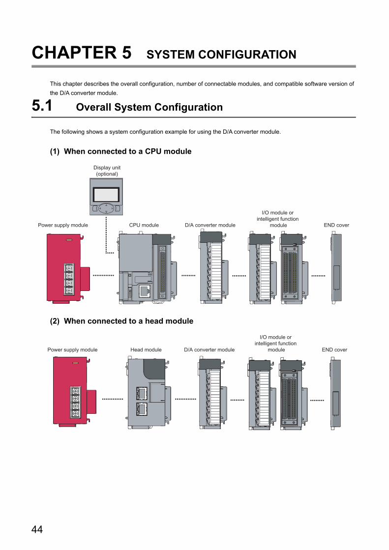
CHAPTER 5 SYSTEM CONFIGURATION
This chapter describes the overall configuration, number of connectable modules, and compatible software version of
the D/A converter module.
5.1 Overall System Configuration
The following shows a system configuration example for using the D/A converter module.
(1) When connected to a CPU module
(2) When connected to a head module
Power supply module CPU module
Display unit(optional)
I/O module or intelligent function
module END coverD/A converter module
Power supply module Head module
I/O module or intelligent function
module END coverD/A converter module
44
CHAPTER 5 SYSTEM CONFIGURATION
5
5.2
Ap
plica
ble
Syste
m
5.2 Applicable System
(1) Number of connectable modulesFor the number of connectable modules, refer to the following.
MELSEC-L CPU Module User's Manual (Hardware Design, Maintenance and Inspection)
MELSEC-L CC-Link IE Field Network Head Module User's Manual
(2) Compatible software versionFor compatible software version, refer to the following.
(a) L60DA4
(b) L60DAVL8, L60DAIL8
5.3 Restrictions When D/A Converter Module is Connected to Head Module
The following describes the restriction when the D/A converter module is connected to a head module.
• Dedicated instruction cannot be used.
Software Version
GX Works2 Version 1.20W or later
GX Developer Version 8.88S or later
GX Configurator-DA Version 2.11M or later
Software Version
GX Works2 Version 1.545T or later
GX Developer Version 8.88S or later
GX Configurator-DA Not available
45
CHAPTER 6 INSTALLATION AND WIRING
This chapter describes the installation and wiring of the D/A converter module.
6.1 Installation Environment and Installation Position
For precautions for installation environment and installation position, refer to the following.
MELSEC-L CPU Module User's Manual (Hardware Design, Maintenance and Inspection)
MELSEC-L CC-Link IE Field Network Head Module User's Manual
46
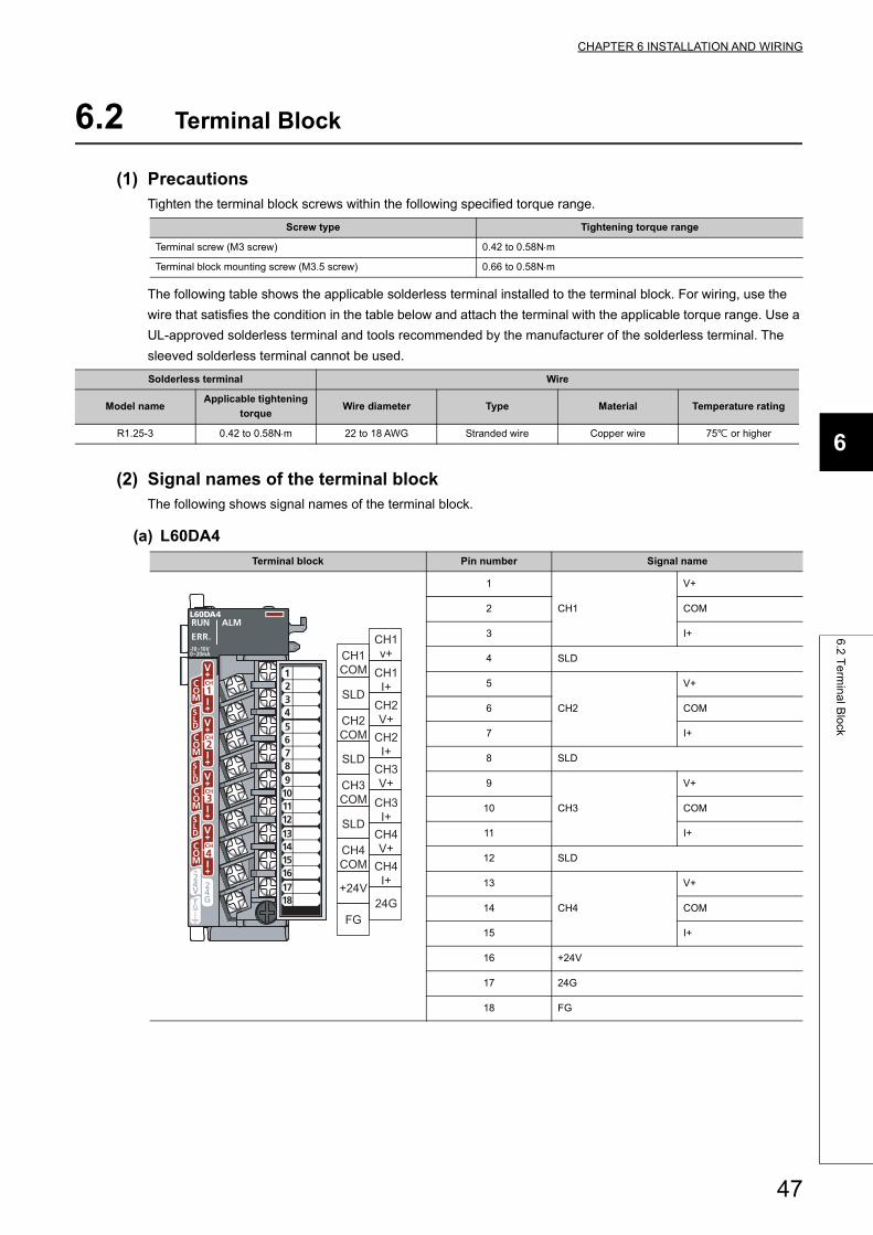
CHAPTER 6 INSTALLATION AND WIRING
6
6.2
Te
rmin
al B
lock
6.2 Terminal Block
(1) PrecautionsTighten the terminal block screws within the following specified torque range.
The following table shows the applicable solderless terminal installed to the terminal block. For wiring, use the
wire that satisfies the condition in the table below and attach the terminal with the applicable torque range. Use a
UL-approved solderless terminal and tools recommended by the manufacturer of the solderless terminal. The
sleeved solderless terminal cannot be used.
(2) Signal names of the terminal blockThe following shows signal names of the terminal block.
(a) L60DA4
Screw type Tightening torque range
Terminal screw (M3 screw) 0.42 to 0.58Nm
Terminal block mounting screw (M3.5 screw) 0.66 to 0.58Nm
Solderless terminal Wire
Model nameApplicable tightening
torqueWire diameter Type Material Temperature rating
R1.25-3 0.42 to 0.58Nm 22 to 18 AWG Stranded wire Copper wire 75 or higher
Terminal block Pin number Signal name
1
CH1
V+
2 COM
3 I+
4 SLD
5
CH2
V+
6 COM
7 I+
8 SLD
9
CH3
V+
10 COM
11 I+
12 SLD
13
CH4
V+
14 COM
15 I+
16 +24V
17 24G
18 FG
CH1v+
CH1I+
CH2V+
CH2I+
CH3V+
CH3I+
CH4V+
CH4I+
24G
CH1COM
SLD
CH2COM
SLD
CH3COM
SLD
CH4COM
+24V
FG
47
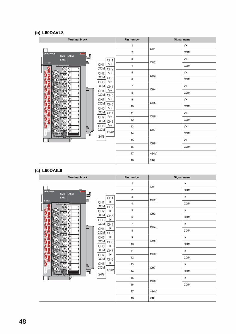
(b) L60DAVL8
(c) L60DAIL8
Terminal block Pin number Signal name
1CH1
V+
2 COM
3CH2
V+
4 COM
5CH3
V+
6 COM
7CH4
V+
8 COM
9CH5
V+
10 COM
11CH6
V+
12 COM
13CH7
V+
14 COM
15CH8
V+
16 COM
17 +24V
18 24G
Terminal block Pin number Signal name
1CH1
I+
2 COM
3CH2
I+
4 COM
5CH3
I+
6 COM
7CH4
I+
8 COM
9CH5
I+
10 COM
11CH6
I+
12 COM
13CH7
I+
14 COM
15CH8
I+
16 COM
17 +24V
18 24G
CH1V+
CH2V+
CH3V+
CH4V+
CH5V+
CH6V+
CH7V+
CH8V+
+24V
CH1COMCH2COMCH3COMCH4COMCH5COMCH6COMCH7COMCH8COM
24G
CH1I+
CH2I+
CH3I+
CH4I+
CH5I+
CH6I+
CH7I+
CH8I+
+24V
CH1COMCH2COMCH3COMCH4COMCH5COMCH6COMCH7COMCH8COM
24G
48
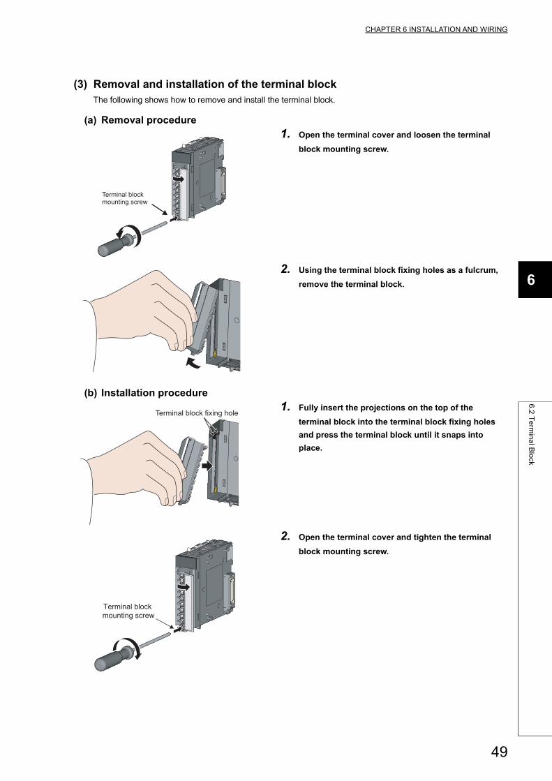
CHAPTER 6 INSTALLATION AND WIRING
6
6.2
Te
rmin
al B
lock
(3) Removal and installation of the terminal blockThe following shows how to remove and install the terminal block.
(a) Removal procedure
(b) Installation procedure
1. Open the terminal cover and loosen the terminal
block mounting screw.
2. Using the terminal block fixing holes as a fulcrum,
remove the terminal block.
1. Fully insert the projections on the top of the
terminal block into the terminal block fixing holes
and press the terminal block until it snaps into
place.
2. Open the terminal cover and tighten the terminal
block mounting screw.
Terminal block mounting screw
Terminal block fixing hole
Terminal block
mounting screw
49
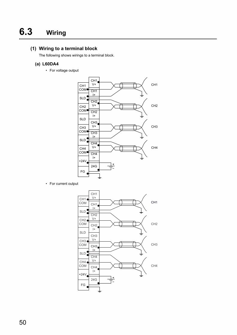
6.3 Wiring
(1) Wiring to a terminal blockThe following shows wirings to a terminal block.
(a) L60DA4
• For voltage output
• For current output
CH1COM
SLD
SLD
SLD
+24V24G
FG
CH2COM
CH3COM
CH4COM
CH1V+
CH1I+
CH2V+
CH2I+
CH3V+
CH3I+
CH4V+
CH4I+
CH1
CH2
CH3
CH4
CH1COM
SLD
SLD
SLD
+24V24G
FG
CH2COM
CH3COM
CH4COM
CH1V+
CH1I+
CH2V+
CH2I+
CH3V+
CH3I+
CH4V+
CH4I+
CH1
CH2
CH3
CH4
50
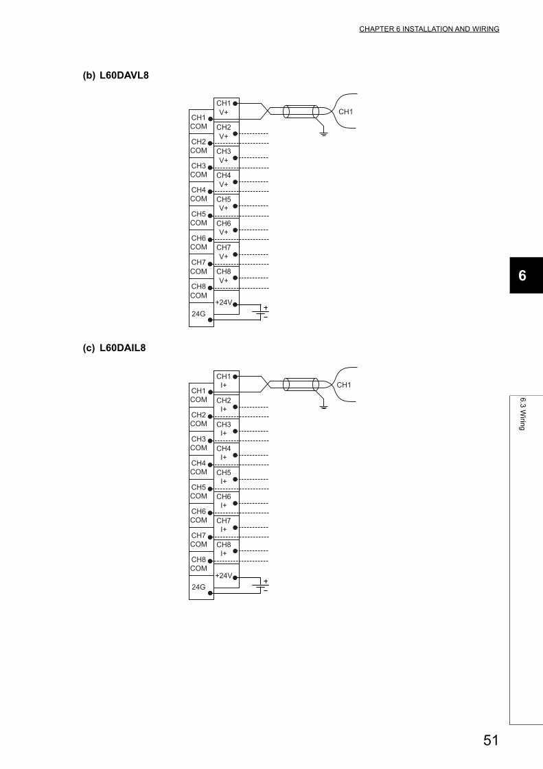
CHAPTER 6 INSTALLATION AND WIRING
6
6.3
Wirin
g
(b) L60DAVL8
(c) L60DAIL8
CH1COM
CH2COM
CH4COM
CH8COM
CH3COM
CH5COM
CH7COM
24G
CH1V+
CH2V+
CH3V+
CH4V+
CH5V+
CH6V+
CH7V+
CH8V+
+24V
CH6COM
CH1
CH1COM
CH2COM
CH4COM
CH8COM
CH3COM
CH5COM
CH7COM
24G
CH1I+
CH2I+
CH3I+
CH4I+
CH5I+
CH6I+
CH7I+
CH8I+
+24V
CH6COM
CH1
51
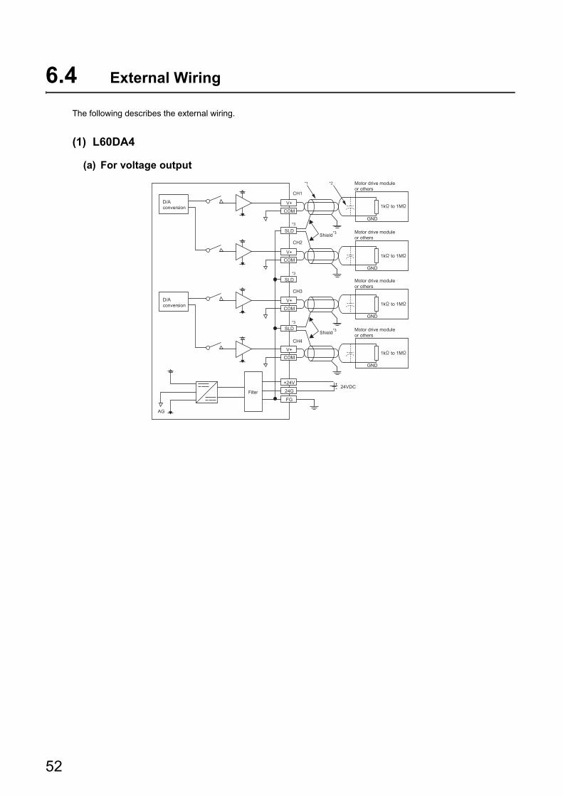
6.4 External Wiring
The following describes the external wiring.
(1) L60DA4
(a) For voltage output
*1 *2
*3
*3
*3
Motor drive module or others
1k to 1M
GND
1k to 1M
GND
1k to 1M
GND
1k to 1M
GND
D/A conversion
D/A conversion
AG
Filter24VDC
CH1
CH2
V+
V+
COM
CH3
CH4
V+
COM
V+
+24V
24G
FG
COM
COM
SLD
SLD
SLD
Motor drive module or others
Motor drive module or others
Motor drive module or othersShield*3
Shield*3
52
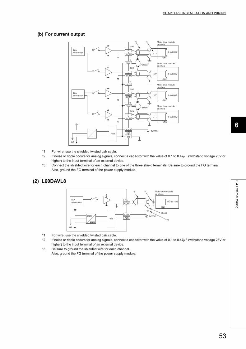
CHAPTER 6 INSTALLATION AND WIRING
6
6.4
Exte
rna
l Wirin
g
(b) For current output
*1 For wire, use the shielded twisted pair cable.*2 If noise or ripple occurs for analog signals, connect a capacitor with the value of 0.1 to 0.47F (withstand voltage 25V or
higher) to the input terminal of an external device.*3 Connect the shielded wire for each channel to one of the three shield terminals. Be sure to ground the FG terminal.
Also, ground the FG terminal of the power supply module.
(2) L60DAVL8
*1 For wire, use the shielded twisted pair cable.*2 If noise or ripple occurs for analog signals, connect a capacitor with the value of 0.1 to 0.47F (withstand voltage 25V or
higher) to the input terminal of an external device.*3 Be sure to ground the shielded wire for each channel.
Also, ground the FG terminal of the power supply module.
*1 *2
*3
*3
*3
Motor drive module or others
0 to 600
GND
GND
GND
GND
D/A conversion
D/A conversion
AG
Filter24VDC
CH1
CH2
I+
I+
COM
CH3
CH4
I+
COM
I+
+24V
24G
FG
COM
COM
SLD
SLD
SLD
Motor drive module or others
Motor drive module or others
Motor drive module or others
0 to 600
0 to 600
0 to 600
Shield*3
Shield*3
*1 *2 Motor drive module or others
1k to 1M
GND
D/A conversion
AG
Filter24VDC
V+
COM
+24V
24G
Shield
*3
53
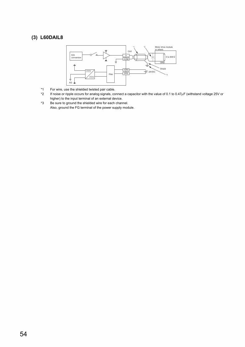
(3) L60DAIL8
*1 For wire, use the shielded twisted pair cable.*2 If noise or ripple occurs for analog signals, connect a capacitor with the value of 0.1 to 0.47F (withstand voltage 25V or
higher) to the input terminal of an external device.*3 Be sure to ground the shielded wire for each channel.
Also, ground the FG terminal of the power supply module.
*1 *2 Motor drive module or others
0 to 600
GND
D/A conversion
AG
Filter24VDC
CH1
I+
COM
+24V
24G*3
Shield
54
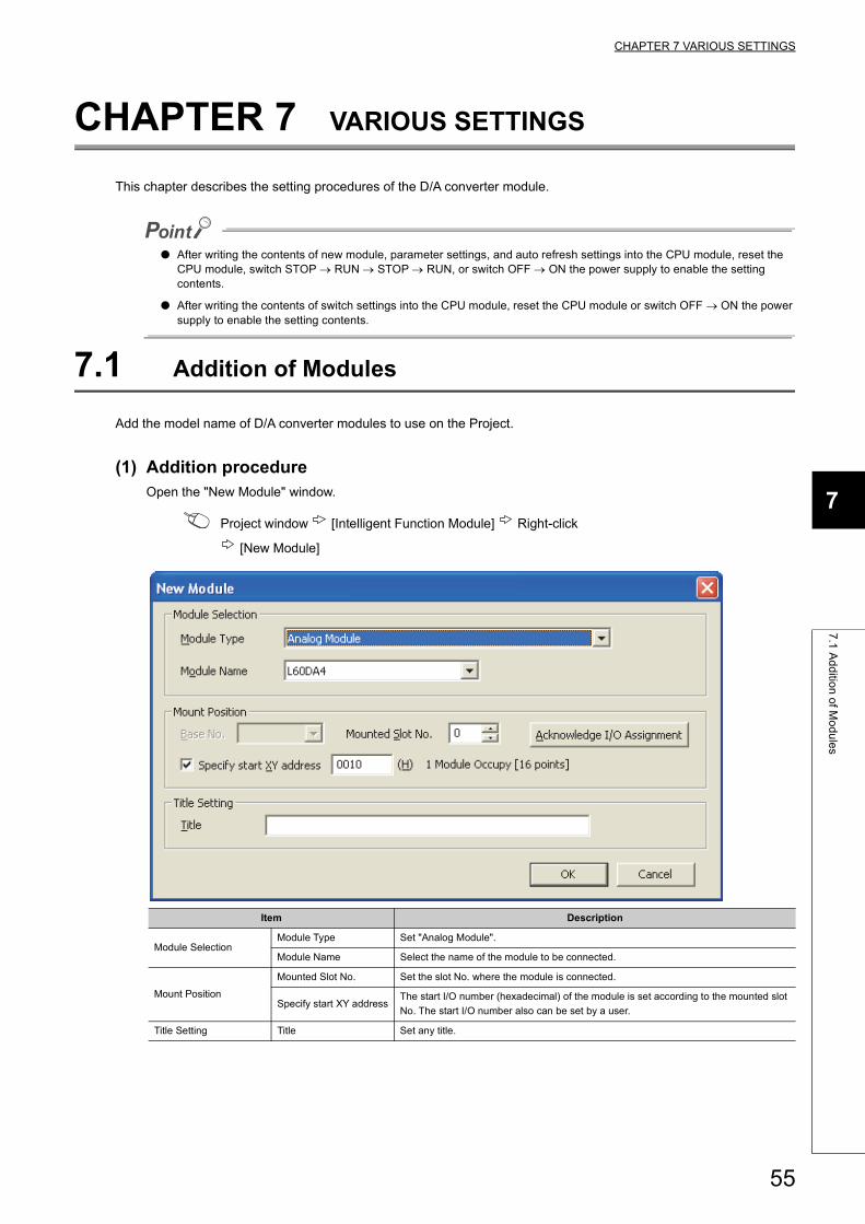
CHAPTER 7 VARIOUS SETTINGS
7
7.1
Ad
ditio
n o
f Mo
du
les
CHAPTER 7 VARIOUS SETTINGS
This chapter describes the setting procedures of the D/A converter module.
● After writing the contents of new module, parameter settings, and auto refresh settings into the CPU module, reset the CPU module, switch STOP RUN STOP RUN, or switch OFF ON the power supply to enable the setting contents.
● After writing the contents of switch settings into the CPU module, reset the CPU module or switch OFF ON the power supply to enable the setting contents.
7.1 Addition of Modules
Add the model name of D/A converter modules to use on the Project.
(1) Addition procedureOpen the "New Module" window.
Project window [Intelligent Function Module] Right-click
[New Module]
Item Description
Module SelectionModule Type Set "Analog Module".
Module Name Select the name of the module to be connected.
Mount Position
Mounted Slot No. Set the slot No. where the module is connected.
Specify start XY addressThe start I/O number (hexadecimal) of the module is set according to the mounted slot
No. The start I/O number also can be set by a user.
Title Setting Title Set any title.
55
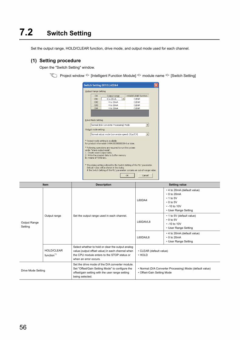
7.2 Switch Setting
Set the output range, HOLD/CLEAR function, drive mode, and output mode used for each channel.
(1) Setting procedureOpen the "Switch Setting" window.
Project window [Intelligent Function Module] module name [Switch Setting]
Item Description Setting value
Output Range
Setting
Output range Set the output range used in each channel.
L60DA4
• 4 to 20mA (default value)
• 0 to 20mA
• 1 to 5V
• 0 to 5V
• -10 to 10V
• User Range Setting
L60DAVL8
• 1 to 5V (default value)
• 0 to 5V
• -10 to 10V
• User Range Setting
L60DAIL8
• 4 to 20mA (default value)
• 0 to 20mA
• User Range Setting
HOLD/CLEAR
function*1
Select whether to hold or clear the output analog
value (output offset value) in each channel when
the CPU module enters to the STOP status or
when an error occurs.
• CLEAR (default value)
• HOLD
Drive Mode Setting
Set the drive mode of the D/A converter module.
Set "Offset/Gain Setting Mode" to configure the
offset/gain setting with the user range setting
being selected.
• Normal (D/A Converter Processing) Mode (default value)
• Offset-Gain Setting Mode
56
CHAPTER 7 VARIOUS SETTINGS
7
7.2
Sw
itch S
ettin
g
*1 The operation of the D/A converter module in the normal output mode differs from the operation in the wave output mode. For details, refer to the following.
• Analog Output HOLD/CLEAR Function ( Page 71, Section 8.4)
(a) Intelligent function module switch setting (Switch 1 to 5)
The items described in (1) also can be set in Switch 1 to 5 of the intelligent function module switch setting of
"PLC parameter". The following are the switches to set each item.
• Switch 1, Switch 2: Output range setting
• Switch 3: HOLD/CLEAR function setting
• Switch 4: Drive mode setting, output mode setting
For the setting procedure, refer to the following.
• Intelligent function module switch setting ( Page 238, Appendix 9.1 (2))
Though the example of procedure is for GX Developer, same settings and values can be used for GX Works2
as well.
Output mode settingSet the output mode of the D/A converter
module.
L60DA4
• Normal output mode (conversion speed:
20s/CH) (default value)
• Wave output mode (conversion speed:
50s/CH)
• Wave output mode (conversion speed:
80s/CH)
L60DAVL8• Normal Output Mode (default value)
• Wave Output Mode
L60DAIL8• Normal Output Mode (default value)
• Wave Output Mode
Item Description Setting value
57
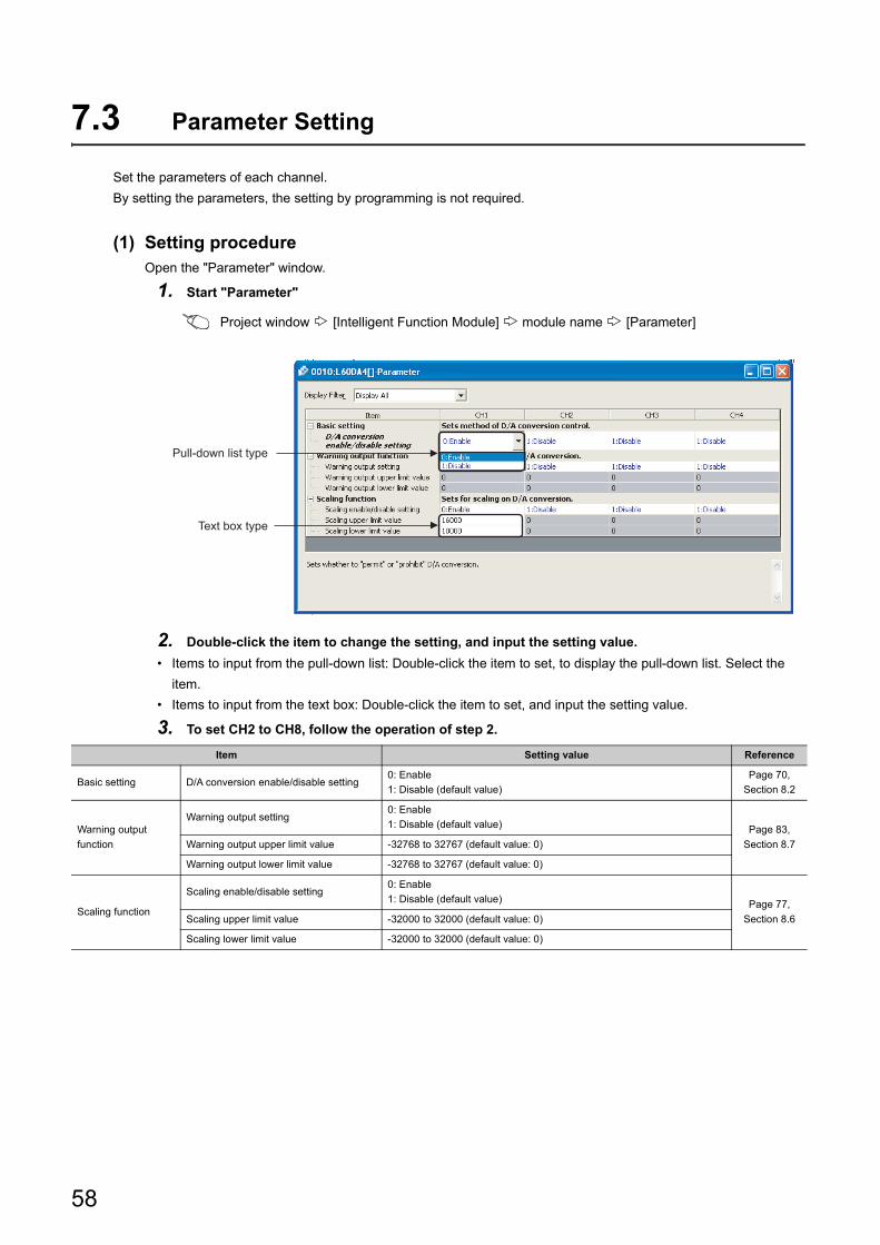
7.3 Parameter Setting
Set the parameters of each channel.
By setting the parameters, the setting by programming is not required.
(1) Setting procedureOpen the "Parameter" window.
1. Start "Parameter"
Project window [Intelligent Function Module] module name [Parameter]
2. Double-click the item to change the setting, and input the setting value.
• Items to input from the pull-down list: Double-click the item to set, to display the pull-down list. Select the
item.
• Items to input from the text box: Double-click the item to set, and input the setting value.
3. To set CH2 to CH8, follow the operation of step 2.
Item Setting value Reference
Basic setting D/A conversion enable/disable setting0: Enable
1: Disable (default value)
Page 70,
Section 8.2
Warning output
function
Warning output setting0: Enable
1: Disable (default value) Page 83,
Section 8.7Warning output upper limit value -32768 to 32767 (default value: 0)
Warning output lower limit value -32768 to 32767 (default value: 0)
Scaling function
Scaling enable/disable setting0: Enable
1: Disable (default value) Page 77,
Section 8.6Scaling upper limit value -32000 to 32000 (default value: 0)
Scaling lower limit value -32000 to 32000 (default value: 0)
Pull-down list type
Text box type
58
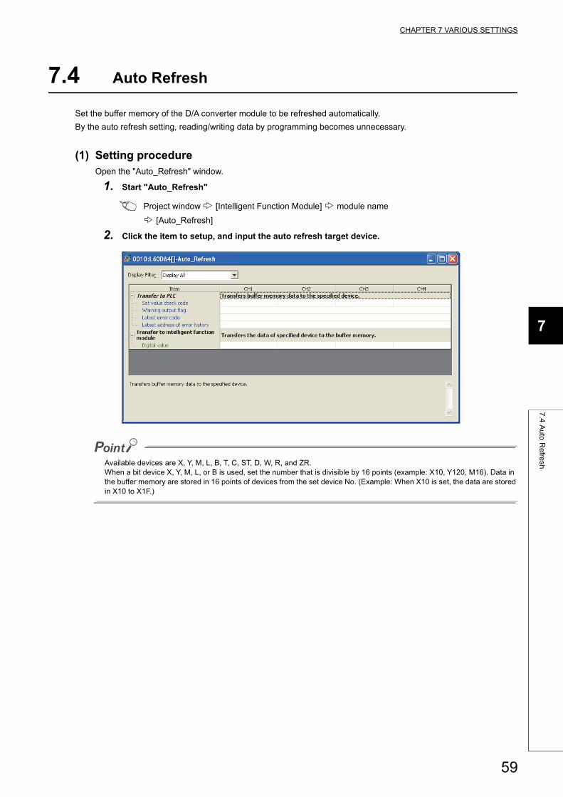
CHAPTER 7 VARIOUS SETTINGS
7
7.4
Au
to R
efre
sh
7.4 Auto Refresh
Set the buffer memory of the D/A converter module to be refreshed automatically.
By the auto refresh setting, reading/writing data by programming becomes unnecessary.
(1) Setting procedureOpen the "Auto_Refresh" window.
1. Start "Auto_Refresh"
Project window [Intelligent Function Module] module name
[Auto_Refresh]
2. Click the item to setup, and input the auto refresh target device.
Available devices are X, Y, M, L, B, T, C, ST, D, W, R, and ZR.When a bit device X, Y, M, L, or B is used, set the number that is divisible by 16 points (example: X10, Y120, M16). Data in the buffer memory are stored in 16 points of devices from the set device No. (Example: When X10 is set, the data are stored in X10 to X1F.)
59
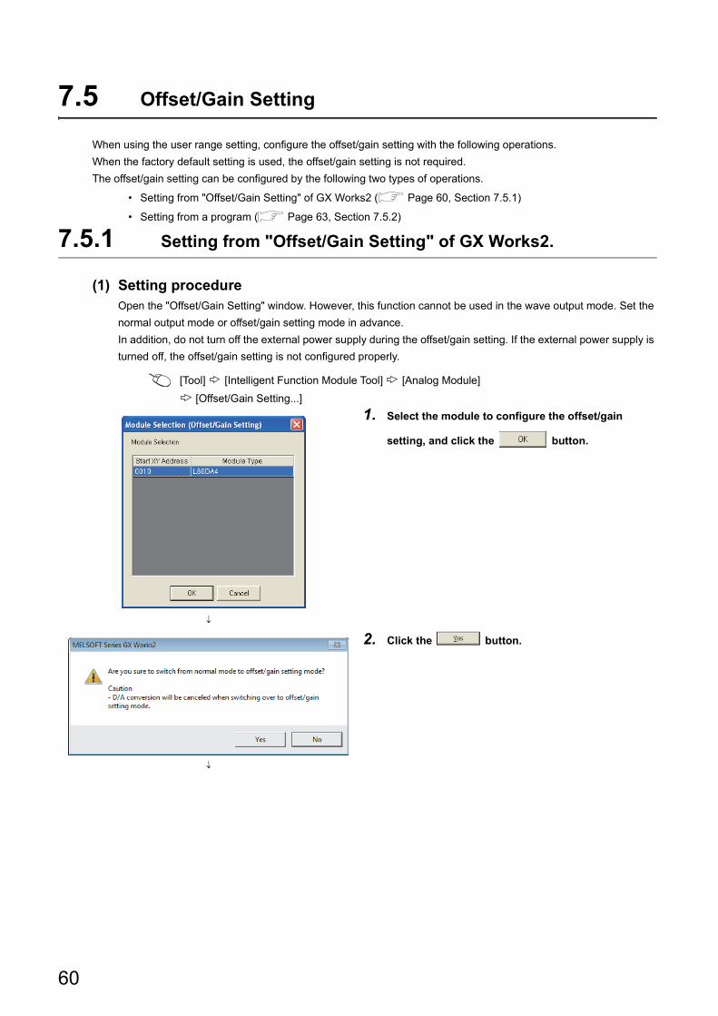
7.5 Offset/Gain Setting
When using the user range setting, configure the offset/gain setting with the following operations.
When the factory default setting is used, the offset/gain setting is not required.
The offset/gain setting can be configured by the following two types of operations.
• Setting from "Offset/Gain Setting" of GX Works2 ( Page 60, Section 7.5.1)
• Setting from a program ( Page 63, Section 7.5.2)
7.5.1 Setting from "Offset/Gain Setting" of GX Works2.
(1) Setting procedureOpen the "Offset/Gain Setting" window. However, this function cannot be used in the wave output mode. Set the
normal output mode or offset/gain setting mode in advance.
In addition, do not turn off the external power supply during the offset/gain setting. If the external power supply is
turned off, the offset/gain setting is not configured properly.
[Tool] [Intelligent Function Module Tool] [Analog Module]
[Offset/Gain Setting...]
1. Select the module to configure the offset/gain
setting, and click the button.
2. Click the button.
60
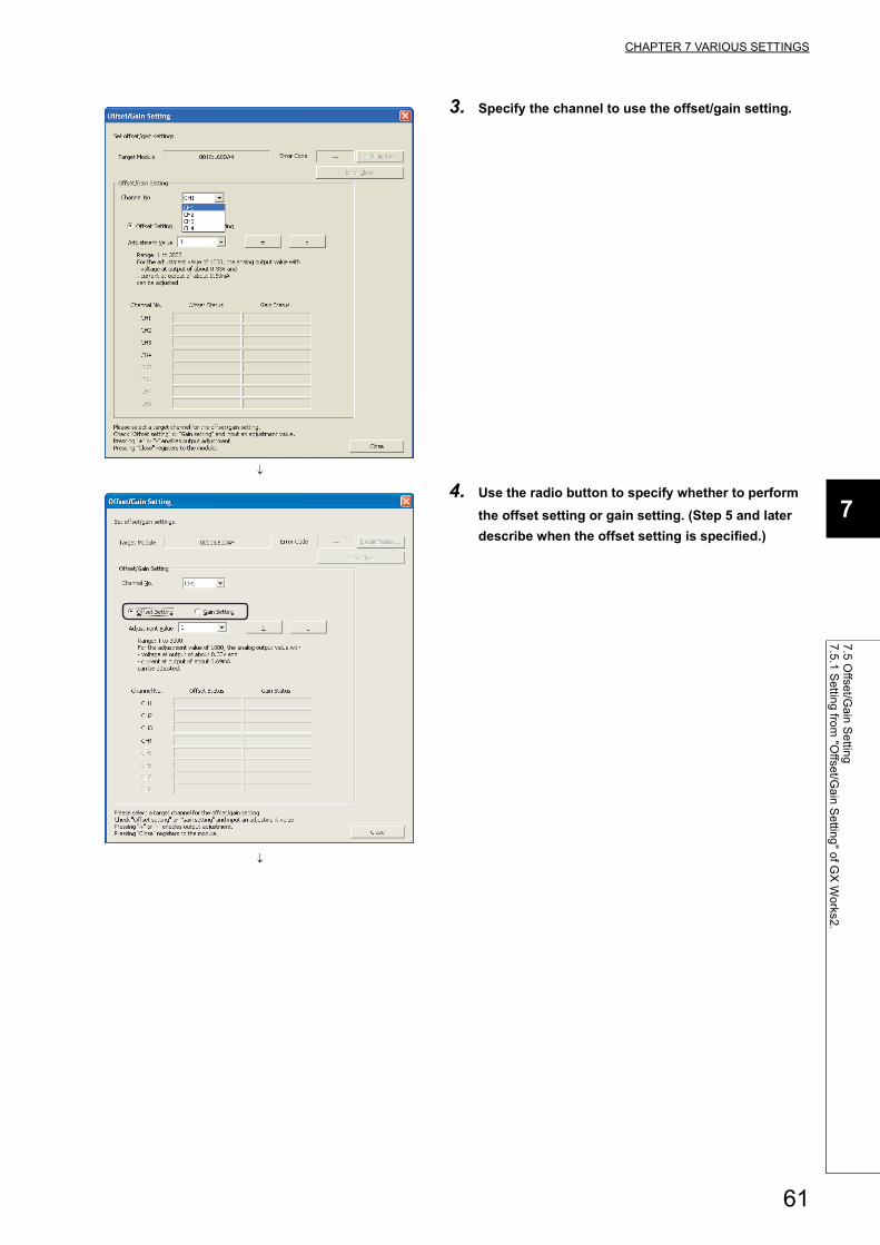
CHAPTER 7 VARIOUS SETTINGS
7
7.5
Offse
t/Ga
in S
ettin
g7
.5.1
Se
tting
from
"Offse
t/Ga
in S
ettin
g" o
f GX
Wo
rks2.
3. Specify the channel to use the offset/gain setting.
4. Use the radio button to specify whether to perform
the offset setting or gain setting. (Step 5 and later
describe when the offset setting is specified.)
61
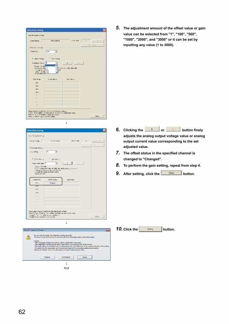
5. The adjustment amount of the offset value or gain
value can be selected from "1", "100", "500",
"1000", "2000", and "3000" or it can be set by
inputting any value (1 to 3000).
6. Clicking the or button finely
adjusts the analog output voltage value or analog
output current value corresponding to the set
adjusted value.
7. The offset status in the specified channel is
changed to "Changed".
8. To perform the gain setting, repeat from step 4.
9. After setting, click the button.
10.Click the button.
End
62
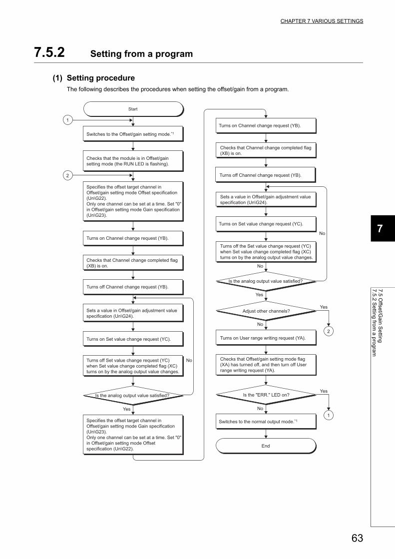
CHAPTER 7 VARIOUS SETTINGS
7
7.5
Offse
t/Ga
in S
ettin
g7
.5.2
Se
tting
from
a p
rog
ram
7.5.2 Setting from a program
(1) Setting procedureThe following describes the procedures when setting the offset/gain from a program.
1
2
Switches to the Offset/gain setting mode.*1
Checks that the module is in Offset/gain
setting mode (the RUN LED is flashing).
Turns on Channel change request (YB).
Turns off Channel change request (YB).
Turns on Set value change request (YC).
Turns on User range writing request (YA).
Switches to the normal output mode.*1
End
Checks that Offset/gain setting mode flag
(XA) has turned off, and then turn off User
range writing request (YA).
Checks that Channel change completed flag
(XB) is on.
Sets a value in Offset/gain adjustment value
specification (Un\G24).
Turns off the Set value change request (YC)
when Set value change completed flag (XC)
turns on by the analog output value changes.
Turns on Channel change request (YB).
Turns off Channel change request (YB).
Turns on Set value change request (YC).
Is the analog output value satisfied?
Is the analog output value satisfied?
Adjust other channels?
Is the "ERR." LED on?
Turns off Set value change request (YC)
when Set value change completed flag (XC)
turns on by the analog output value changes.
Checks that Channel change completed flag
(XB) is on.
Sets a value in Offset/gain adjustment value
specification (Un\G24).
Specifies the offset target channel in
Offset/gain setting mode Offset specification
(Un\G22).
Only one channel can be set at a time. Set "0"
in Offset/gain setting mode Gain specification
(Un\G23).
Specifies the offset target channel in
Offset/gain setting mode Gain specification
(Un\G23).
Only one channel can be set at a time. Set "0"
in Offset/gain setting mode Offset
specification (Un\G22).
Yes
Yes
No
No
No
No
No
Yes
1
Yes
2
Start
63
*1 The following shows the procedure for switching the mode (normal output mode offset/gain setting mode or offset/gain setting mode normal output mode).
• Dedicated instruction (G(P).OFFGAN) ( Page 223, Appendix 5.2)• Setting to Mode switching setting (Un\G158, Un\G159) and OFF ON OFF of Operating condition setting
request (Y9) ( Page 198, Appendix 2 (15))
• Switch Setting ( Page 56, Section 7.2 (1))The wave output mode cannot be switched to the offset/gain setting mode.
● Configure the offset/gain setting in accordance with the actual use situation.
● Offset and gain values are recorded in the flash memory in the D/A converter module by turning OFF ON OFF User range writing request (YA). Once recorded, the values are not deleted even after turning the power off.When the values are written 26 times in succession, an error occurs to prevent an improper write to the flash memory. The error code (162) is stored in Latest error code (Un\G19), Error flag (XF) turns on, and the ERR. LED turns on.
● Configure the offset/gain setting in the range satisfying the following condition.When the setting value out of the range is configured, the resolution and accuracy of the module may not fall within the range shown in the following performance specifications.
• I/O Conversion Characteristic of D/A Conversion ( Page 216, Appendix 3)
● Configure the offset/gain setting for each channel.When settings are configured for offset and gain channels at the same time, an error occurs. The error code (500) is stored in Latest error code (Un\G19), Error flag (XF) turns on, and the ERR. LED turns on.
● When error occurs even in one channel, offset/gain value is not written to the module.Check the value in Latest error code (Un\G19) and perform the following procedures to reconfigure the offset/gain setting from the beginning.
• Error Code List ( Page 171, Section 11.4)
● When the mode is switched from the offset/gain setting mode to the normal output mode by the dedicated instruction (G(P).OFFGAN) or Mode switching setting (Un\G158, Un\G159), Module READY (X0) turns on.Note the initial setting process is executed at the switching of the mode if the sequence program executes the initial setting at Module READY (X0) ON.
● When the external power supply is off, Set value change completed flag (XC) does not turn on even though Set value change request (YC) is turned on. Turn on the external power supply, and turn on and off Set value change request (YC) again.
(2) Program example
(a) Device
Ex. I/O number of D/A converter module is X/Y30 to X/Y3F
The following shows the devices used in the program example.
Device Function
M0 Channel selection
M2 Offset setting
M3 Gain setting
M4 Offset/gain setting channel change command
M5 Mode switching
M6 Analog output value adjustment command
M7 Command to write offset/gain setting values to the module
M8 Adjustment amount setting
M50 Signal for checking the offset/gain setting mode
M51 Signal for checking the normal output mode
D0 Channel-specified storage device
D1 Adjustment amount setting storage device
D2 Storage device for the setting value of the dedicated instruction (G(P).OFFGAN)
M100 Module READY checking flag
64
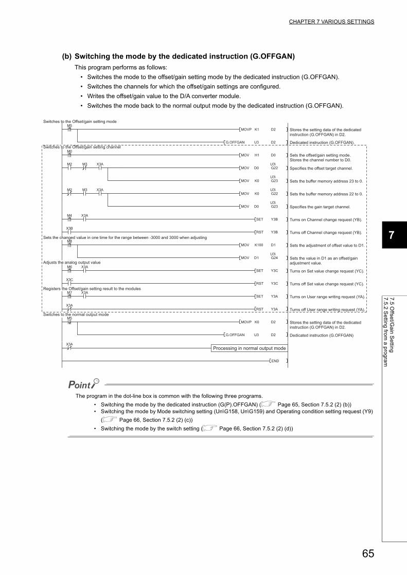
CHAPTER 7 VARIOUS SETTINGS
7
7.5
Offse
t/Ga
in S
ettin
g7
.5.2
Se
tting
from
a p
rog
ram
(b) Switching the mode by the dedicated instruction (G.OFFGAN)
This program performs as follows:
• Switches the mode to the offset/gain setting mode by the dedicated instruction (G.OFFGAN).
• Switches the channels for which the offset/gain settings are configured.
• Writes the offset/gain value to the D/A converter module.
• Switches the mode back to the normal output mode by the dedicated instruction (G.OFFGAN).
The program in the dot-line box is common with the following three programs.
• Switching the mode by the dedicated instruction (G(P).OFFGAN) ( Page 65, Section 7.5.2 (2) (b))• Switching the mode by Mode switching setting (Un\G158, Un\G159) and Operating condition setting request (Y9)
( Page 66, Section 7.5.2 (2) (c))
• Switching the mode by the switch setting ( Page 66, Section 7.5.2 (2) (d))
Processing in normal output mode
Switches to the normal output mode
Registers the Offset/gain setting result to the modules
Adjusts the analog output value
Sets the changed value in one time for the range between -3000 and 3000 when adjusting
Switches to the Offset/gain setting channel
Switches to the Offset/gain setting mode
Stores the setting data of the dedicated instruction (G.OFFGAN) in D2.
Dedicated instruction (G.OFFGAN).
Sets the offset/gain setting mode. Stores the channel number to D0.
Specifies the offset target channel.
Sets the buffer memory address 23 to 0.
Sets the buffer memory address 22 to 0.
Specifies the gain target channel.
Turns on Channel change request (YB).
Turns off Channel change request (YB).
Sets the adjustment of offset value to D1.
Sets the value in D1 as an offset/gain adjustment value.
Turns on Set value change request (YC).
Turns off Set value change request (YC).
Turns on User range writing request (YA).
Turns off User range writing request (YA).
Stores the setting data of the dedicated instruction (G.OFFGAN) in D2.
Dedicated instruction (G.OFFGAN)
65
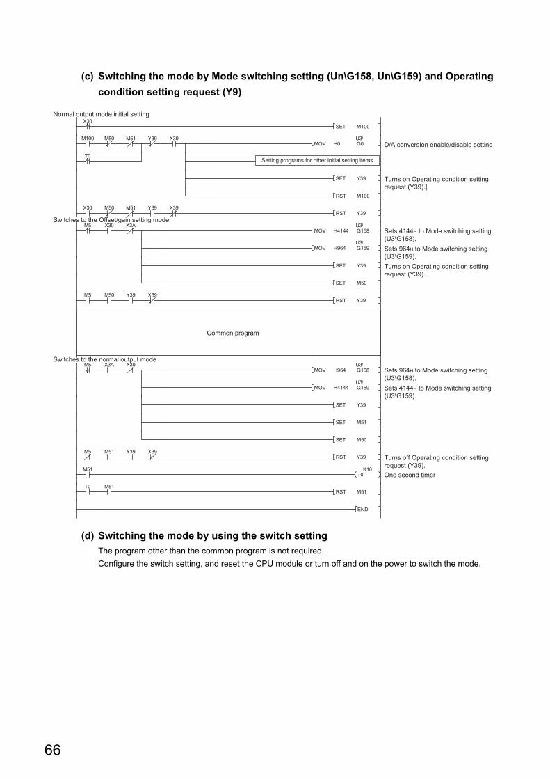
(c) Switching the mode by Mode switching setting (Un\G158, Un\G159) and Operating
condition setting request (Y9)
(d) Switching the mode by using the switch setting
The program other than the common program is not required.
Configure the switch setting, and reset the CPU module or turn off and on the power to switch the mode.
Setting programs for other initial setting items
Common program
D/A conversion enable/disable setting
Turns on Operating condition settingrequest (Y39).]
Sets 4144H to Mode switching setting(U3\G158).Sets 964H to Mode switching setting(U3\G159).Turns on Operating condition settingrequest (Y39).
Sets 964H to Mode switching setting(U3\G158).Sets 4144H to Mode switching setting(U3\G159).
Turns off Operating condition settingrequest (Y39).One second timer
Normal output mode initial setting
Switches to the Offset/gain setting mode
Switches to the normal output mode
66
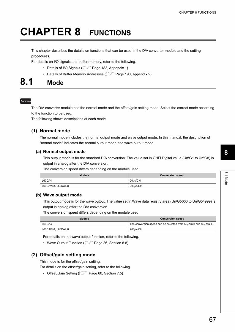
CHAPTER 8 FUNCTIONS
8
8.1
Mo
de
CHAPTER 8 FUNCTIONS
This chapter describes the details on functions that can be used in the D/A converter module and the setting
procedures.
For details on I/O signals and buffer memory, refer to the following.
• Details of I/O Signals ( Page 183, Appendix 1)
• Details of Buffer Memory Addresses ( Page 190, Appendix 2)
8.1 Mode
The D/A converter module has the normal mode and the offset/gain setting mode. Select the correct mode according
to the function to be used.
The following shows descriptions of each mode.
(1) Normal modeThe normal mode includes the normal output mode and wave output mode. In this manual, the description of
"normal mode" indicates the normal output mode and wave output mode.
(a) Normal output mode
This output mode is for the standard D/A conversion. The value set in CH Digital value (Un\G1 to Un\G8) is
output in analog after the D/A conversion.
The conversion speed differs depending on the module used.
(b) Wave output mode
This output mode is for the wave output. The value set in Wave data registry area (Un\G5000 to Un\G54999) is
output in analog after the D/A conversion.
The conversion speed differs depending on the module used.
For details on the wave output function, refer to the following.
• Wave Output Function ( Page 86, Section 8.8)
(2) Offset/gain setting modeThis mode is for the offset/gain setting.
For details on the offset/gain setting, refer to the following.
• Offset/Gain Setting ( Page 60, Section 7.5)
Module Conversion speed
L60DA4 20s/CH
L60DAVL8, L60DAIL8 200s/CH
Module Conversion speed
L60DA4 The conversion speed can be selected from 50s/CH and 80s/CH.
L60DAVL8, L60DAIL8 200s/CH
Common
67
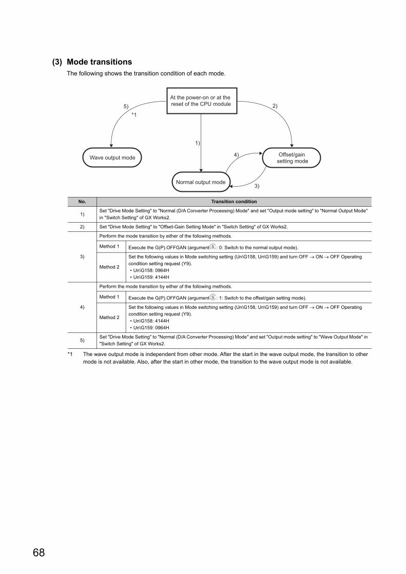
(3) Mode transitionsThe following shows the transition condition of each mode.
*1 The wave output mode is independent from other mode. After the start in the wave output mode, the transition to other mode is not available. Also, after the start in other mode, the transition to the wave output mode is not available.
No. Transition condition
1)Set "Drive Mode Setting" to "Normal (D/A Converter Processing) Mode" and set "Output mode setting" to "Normal Output Mode"
in "Switch Setting" of GX Works2.
2) Set "Drive Mode Setting" to "Offset-Gain Setting Mode" in "Switch Setting" of GX Works2.
3)
Perform the mode transition by either of the following methods.
Method 1 Execute the G(P).OFFGAN (argument : 0: Switch to the normal output mode).
Method 2
Set the following values in Mode switching setting (Un\G158, Un\G159) and turn OFF ON OFF Operating
condition setting request (Y9).
• Un\G158: 0964H
• Un\G159: 4144H
4)
Perform the mode transition by either of the following methods.
Method 1 Execute the G(P).OFFGAN (argument : 1: Switch to the offset/gain setting mode).
Method 2
Set the following values in Mode switching setting (Un\G158, Un\G159) and turn OFF ON OFF Operating
condition setting request (Y9).
• Un\G158: 4144H
• Un\G159: 0964H
5)Set "Drive Mode Setting" to "Normal (D/A Converter Processing) Mode" and set "Output mode setting" to "Wave Output Mode" in
"Switch Setting" of GX Works2.
At the power-on or at the
reset of the CPU module5) 2)
1)
4)
3)Normal output mode
Wave output modeOffset/gain
setting mode
*1
S
S
68
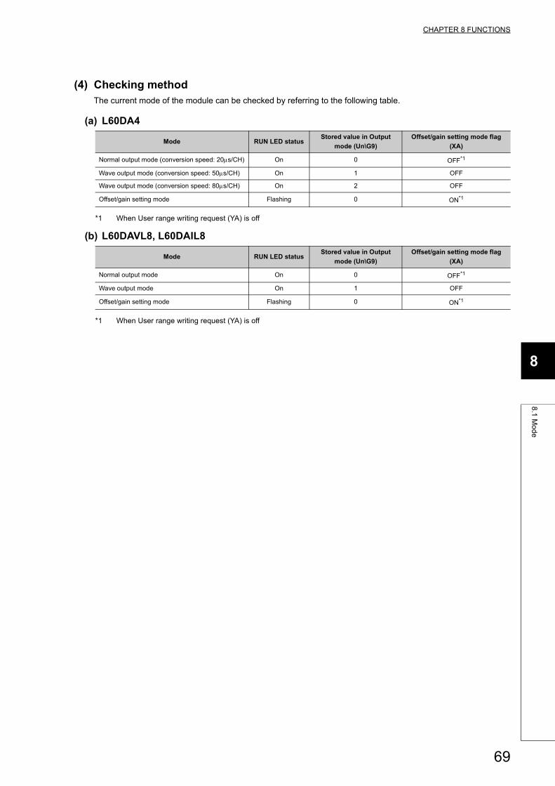
CHAPTER 8 FUNCTIONS
8
8.1
Mo
de
(4) Checking methodThe current mode of the module can be checked by referring to the following table.
(a) L60DA4
*1 When User range writing request (YA) is off
(b) L60DAVL8, L60DAIL8
*1 When User range writing request (YA) is off
Mode RUN LED statusStored value in Output
mode (Un\G9)
Offset/gain setting mode flag
(XA)
Normal output mode (conversion speed: 20s/CH) On 0 OFF*1
Wave output mode (conversion speed: 50s/CH) On 1 OFF
Wave output mode (conversion speed: 80s/CH) On 2 OFF
Offset/gain setting mode Flashing 0 ON*1
Mode RUN LED statusStored value in Output
mode (Un\G9)
Offset/gain setting mode flag
(XA)
Normal output mode On 0 OFF*1
Wave output mode On 1 OFF
Offset/gain setting mode Flashing 0 ON*1
69
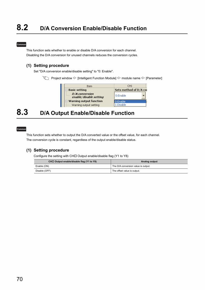
8.2 D/A Conversion Enable/Disable Function
This function sets whether to enable or disable D/A conversion for each channel.
Disabling the D/A conversion for unused channels reduces the conversion cycles.
(1) Setting procedureSet "D/A conversion enable/disable setting" to "0: Enable".
Project window [Intelligent Function Module] module name [Parameter]
8.3 D/A Output Enable/Disable Function
This function sets whether to output the D/A converted value or the offset value, for each channel.
The conversion cycle is constant, regardless of the output enable/disable status.
(1) Setting procedureConfigure the setting with CH Output enable/disable flag (Y1 to Y8)
CH Output enable/disable flag (Y1 to Y8) Analog output
Enable (ON) The D/A conversion value is output.
Disable (OFF) The offset value is output.
Common
Common
70
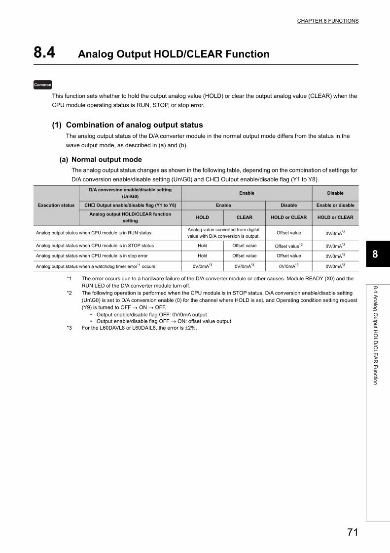
CHAPTER 8 FUNCTIONS
8
8.4
An
alo
g O
utp
ut H
OL
D/C
LE
AR
Fu
nctio
n
8.4 Analog Output HOLD/CLEAR Function
This function sets whether to hold the output analog value (HOLD) or clear the output analog value (CLEAR) when the
CPU module operating status is RUN, STOP, or stop error.
(1) Combination of analog output statusThe analog output status of the D/A converter module in the normal output mode differs from the status in the
wave output mode, as described in (a) and (b).
(a) Normal output mode
The analog output status changes as shown in the following table, depending on the combination of settings for
D/A conversion enable/disable setting (Un\G0) and CH Output enable/disable flag (Y1 to Y8).
*1 The error occurs due to a hardware failure of the D/A converter module or other causes. Module READY (X0) and the RUN LED of the D/A converter module turn off.
*2 The following operation is performed when the CPU module is in STOP status, D/A conversion enable/disable setting (Un\G0) is set to D/A conversion enable (0) for the channel where HOLD is set, and Operating condition setting request (Y9) is turned to OFF ON OFF.
• Output enable/disable flag OFF: 0V/0mA output• Output enable/disable flag OFF ON: offset value output
*3 For the L60DAVL8 or L60DAIL8, the error is 2%.
Execution status
D/A conversion enable/disable setting
(Un\G0)Enable Disable
CH Output enable/disable flag (Y1 to Y8) Enable Disable Enable or disable
Analog output HOLD/CLEAR function
settingHOLD CLEAR HOLD or CLEAR HOLD or CLEAR
Analog output status when CPU module is in RUN statusAnalog value converted from digital
value with D/A conversion is output.Offset value 0V/0mA*3
Analog output status when CPU module is in STOP status Hold Offset value Offset value*2 0V/0mA*3
Analog output status when CPU module is in stop error Hold Offset value Offset value 0V/0mA*3
Analog output status when a watchdog timer error*1 occurs 0V/0mA*3 0V/0mA*3 0V/0mA*3 0V/0mA*3
Common
71
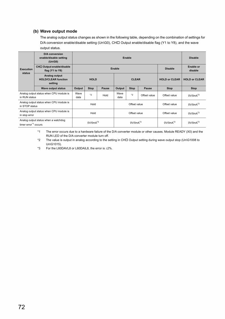
(b) Wave output mode
The analog output status changes as shown in the following table, depending on the combination of settings for
D/A conversion enable/disable setting (Un\G0), CH Output enable/disable flag (Y1 to Y8), and the wave
output status.
*1 The error occurs due to a hardware failure of the D/A converter module or other causes. Module READY (X0) and the RUN LED of the D/A converter module turn off.
*2 The value is output in analog according to the setting in CH Output setting during wave output stop (Un\G1008 to Un\G1015).
*3 For the L60DAVL8 or L60DAIL8, the error is 2%.
Execution
status
D/A conversion
enable/disable setting
(Un\G0)
Enable Disable
CH Output enable/disable
flag (Y1 to Y8)Enable Disable
Enable or
disable
Analog output
HOLD/CLEAR function
setting
HOLD CLEAR HOLD or CLEAR HOLD or CLEAR
Wave output status Output Stop Pause Output Stop Pause Stop Stop
Analog output status when CPU module is
in RUN status
Wave
data*2 Hold
Wave
data*2 Offset value Offset value 0V/0mA*3
Analog output status when CPU module is
in STOP statusHold Offset value Offset value 0V/0mA*3
Analog output status when CPU module is
in stop errorHold Offset value Offset value 0V/0mA*3
Analog output status when a watchdog
timer error*1 occurs0V/0mA*3 0V/0mA*3 0V/0mA*3 0V/0mA*3
72
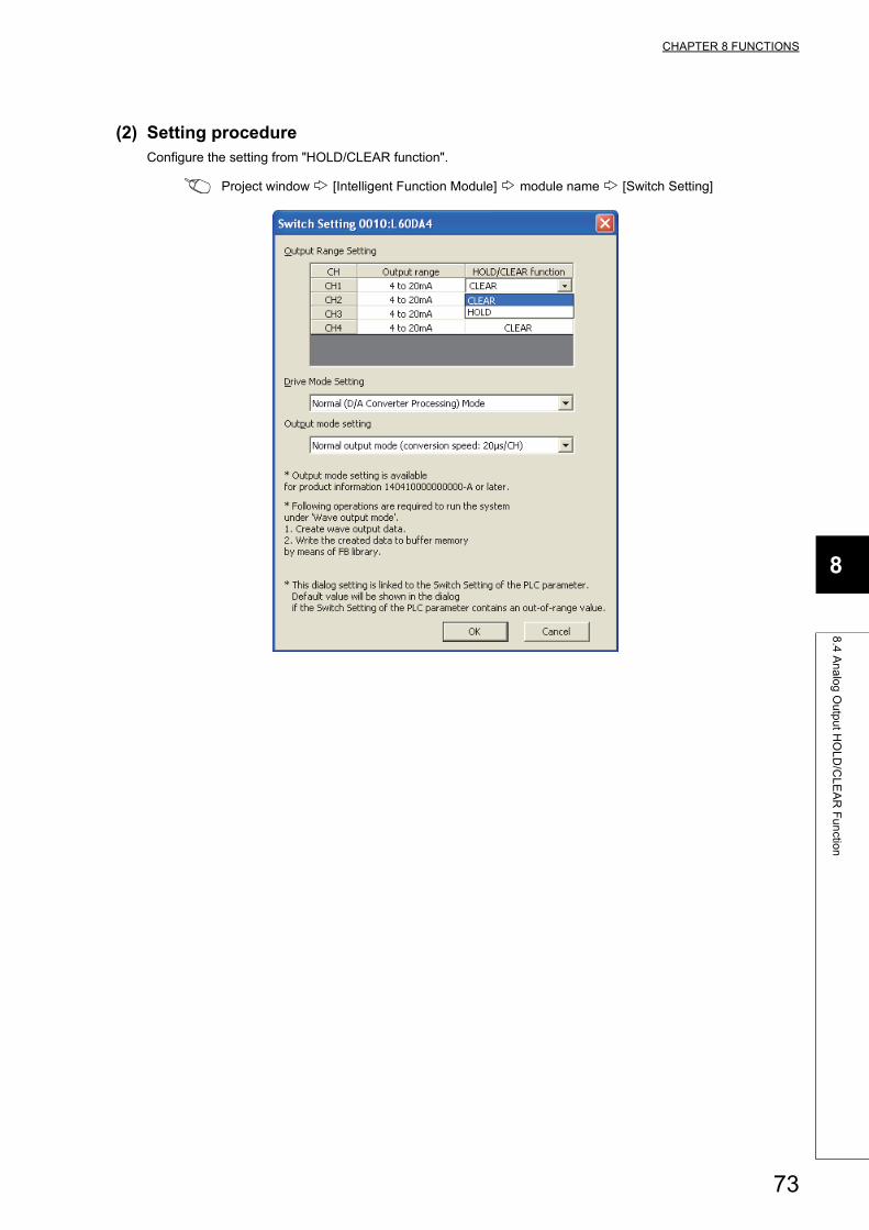
CHAPTER 8 FUNCTIONS
8
8.4
An
alo
g O
utp
ut H
OL
D/C
LE
AR
Fu
nctio
n
(2) Setting procedureConfigure the setting from "HOLD/CLEAR function".
Project window [Intelligent Function Module] module name [Switch Setting]
73
(3) When using the analog output HOLD/CLEAR function with the module
connected to the head moduleThe following describes the conditions for using the analog output HOLD/CLEAR function when the analog I/O
module is connected to the head module.
• Enable the station-based block data assurance of the cyclic data on the send side.
• When a link error occurs, configure the setting to hold the D/A conversion output through "Error time output
mode"*1 of the I/O assignment setting. The analog output HOLD/CLEAR function setting of the switch setting
is disabled.
This setting is enabled for each module. Setting by each channel are not available.
To match the output status given when CPU module is in the stop error or STOP status with that given when a
link error occurs, choose the same setting for the analog output HOLD/CLEAR function setting for all the
channels.
Project window [Parameter] [PLC Parameter] [I/O Assignment]
button
For the block guarantee of cyclic data per station, refer to the following manual.
MELSEC-Q CC-Link IE Field Network Master/Local Module User's Manual
MELSEC-L CC-Link IE Field Network Master/Local Module User's Manual
*1 When the error time output mode is enabled• When a data link stops due to a network error• When a data link stops for the CC-Link IE Field diagnostic of GX Works2
Operating status Error time output mode*1Analog output HOLD/CLEAR function setting
(Make the same setting for all the channels.)
Holds the analog output Hold HOLD
Clears the analog output
(Outputs the offset value)Clear CLEAR
74
CHAPTER 8 FUNCTIONS
8
8.5
An
alo
g O
utp
ut T
est w
he
n C
PU
Mo
du
le is in
ST
OP
Sta
tus
8.5 Analog Output Test when CPU Module is in STOP Status
Analog output tests can be carried out when the CPU module is in the STOP status.
The following functions are enabled during the analog output test.
• Scaling Setting ( Page 77, Section 8.6)
• Warning Output Function ( Page 83, Section 8.7)
When a digital value out of the range is written to each channel, an error (error code: 60) occurs and a check code is
stored in CH Set value check code (Un\G11 to Un\G18).
This section describes the analog output test in the normal output mode. For the analog output test in the wave output
mode, refer to the following.
• Wave output step action function ( Page 126, Section 8.8.4)
(1) Setting procedureFor analog output test, configure the settings in the following procedure in the device test of GX Works2.
1. Set D/A conversion enable/disable setting (Un\G0) to D/A conversion Enable (0) for the channel
where the analog output test is performed.
2. Turn OFF ON Operating condition setting request (Y9).
3. Check that Operating condition setting completed flag (X9) is turned off, and turn ON OFF
Operating condition setting request (Y9).
4. Set the digital value equivalent to the analog value to be output to CH Digital value (Un\G1 to
Un\G8) in buffer memory.
5. Turn OFF ON CH Output enable/disable flag (Y1 to Y8) for the channel where the analog
output test is performed.
*1 When performing the analog output test, set D/A conversion enable/disable setting (Un\G0) to "Enable (0)" beforehand.
Setting combinationD/A conversion enable/disable setting (Un\G0) Enable Disable
CH Output enable/disable flag (Y1 to Y8) Enable Disable Enable Disable
Analog output test Allowed Not allowed Not allowed*1
Common
75
(2) Operation timingBy forcibly turning OFF ON CH Output enable/disable flag (Y1 to Y8) when the CPU module is in the STOP
status, an analog output value is changed from an offset value to a D/A-converted analog value.
The following shows the relation between CH1 Output enable/disable flag (Y1) and analog output value when the
CPU module is in STOP status.
*1 CH1 Output enable/disable flag (Y1) turns OFF with CPU STOP.*2 By forcibly turning the CH1 Output enable/disable flag (Y1) OFF ON, analog output value is changed from offset value
to D/A-converted analog value.
When the module is connected to the head module, analog output tests can be carried out even when the CPU module of the master station causes a stop error.
RUN
Offset value
OFF*1 OFF
ON*2 ON
Offset value
RUNSTOP
A D/A-converted value is output even when the CPU module is in STOP status.
Analog output value converted from digital value
Analog output value converted from digital value
Analog output value converted from digital value
CH1 Output enable/disable flag (Y1)
Analog output value status
CPU module status
76
CHAPTER 8 FUNCTIONS
8
8.6
Sca
ling
fun
ction
8.6 Scaling function
This function scales a digital value into a value within the range of the set scaling lower limit value to scaling upper limit
value. The programming for scale conversion can be omitted.
However, this function cannot be used in the wave output mode.
(1) Concept of scaling settingThe setting for scaling lower and upper limit values differs depending on either the factory default setting or the
user range setting is used for analog output range.
(a) When the factory default setting is used for analog output range
• For the scaling upper limit value, set a value corresponding to the upper limit value of the set analog output
value.
• For the scaling lower limit value, set a value corresponding to the lower limit value of the set analog output
value.
(b) When the user range setting is used for analog output range
• For the scaling upper limit value, set a value corresponding to the gain value.
• For the scaling lower limit value, set a value corresponding to the offset value.
(2) Calculating the scaling valueValues converted using the following formulas are used for D/A conversion.
(Values lower than the decimal point are rounded down in scale conversion.)
(a) When the factory default setting is used for output range
Voltage: 1 to 5 V, 0 to 5 V
Current: 4 to 20 mA, 0 to 20 mA
When the voltage is -10 to 10 V
(b) When the user range setting is used for output range
Item Description
DX Digital value
DMax Maximum digital value of the output range used
DMin Minimum digital value of the output range used
SH Scaling upper limit value
SL Scaling lower limit value
Common
SH - SL
DMax - DMin(DX - SL)=Digital value used for D/A conversion
SH - SL
DMax - DMin(DX - SL) + DMin=Digital value used for D/A conversion
SH - SL
DMax - DMin(DX - SL)=Digital value used for D/A conversion
77
(3) Setting procedure
1. Set "D/A conversion enable/disable setting" to "0: Enable".
Project window [Intelligent Function Module] module name [Parameter]
2. Set "Scaling enable/disable setting" to "0: Enable".
3. Set values for "Scaling upper limit value" and "Scaling lower limit value".
● Your scaling settings must meet the following condition:Scaling upper limit value > Scaling lower limit value
● In the channel where "Scaling enable/disable setting" is set to "0: Enable" in the wave output mode, an error occurs. The error code (21) is stored in Latest error code (Un\G19), Error flag (XF) turns on, and the ERR.LED turns on.
● Even if the input range of the digital value is extended, the resolution does not become higher than that provided when the scaling function is not used.
Item Setting range
Scaling upper limit value-32000 to 32000
Scaling lower limit value
78
CHAPTER 8 FUNCTIONS
8
8.6
Sca
ling
fun
ction
(4) Scaling setting example
Ex. When the settings are configured as shown below for a channel with the output range of 0 to 5V for the
L60DA4
• "Scaling upper limit value": 16000
• "Scaling lower limit value": 4000
The following shows the digital values before and after scaling.
When the output range is set to 0 to 5V for the L60DAVL8, analog output voltage (V) is output according to the
digital value in the same way as the L60DA4.
Digital value Digital value after scaling Analog output voltage (V)
4000 0 0
6400 4000 1
8800 8000 2
11200 12000 3
13600 16000 4
16000 20000 5
0V
5V
Digital value
Analog output voltage (V)
Scaling lower limit
value 4000Scaling upper limit
value 16000
0 20000 20479
79
Ex. When the settings are configured as shown below for a channel with the output range of -10 to 10V for the
L60DA4
• "Scaling upper limit value": 16000
• "Scaling lower limit value": 4000
The following shows the digital values before and after scaling.
When the output range is set to -10 to 10V for the L60DAVL8, analog output voltage (V) is output according to the
digital value in the same way as the L60DA4.
Digital value Digital value after scaling Analog output voltage (V)
4000 -20000 -10
7000 -10000 -5
10000 0 0
13000 10000 5
16000 20000 10
10V
-10V
Digital value
Analog output voltage (V)
Scaling lower limit
value 4000
Scaling upper limit
value 16000
0 20000-20000
10000
20479-20480
80
CHAPTER 8 FUNCTIONS
8
8.6
Sca
ling
fun
ction
Ex. When the settings are configured as shown below for a channel with the user range setting of -8 to 8V for
the L60DA4
• "Scaling upper limit value": 16000
• "Scaling lower limit value": 4000
The following shows the digital values before and after scaling.
When the user range setting is set to -8 to 8V for the L60DAVL8, analog output voltage (V) is output according to
the digital value in the same way as the L60DA4.
Digital value Digital value after scaling Analog output voltage (V)
-8000 -20000 -8
-2000 -10000 -4
4000 0 0
10000 10000 4
16000 20000 8
8V
-8V
Digital value
Analog output voltage (V)
Scaling lower limit
value 4000
Scaling upper limit
value 16000
0 20000-20000
-8000
-20480 20479
0V
81
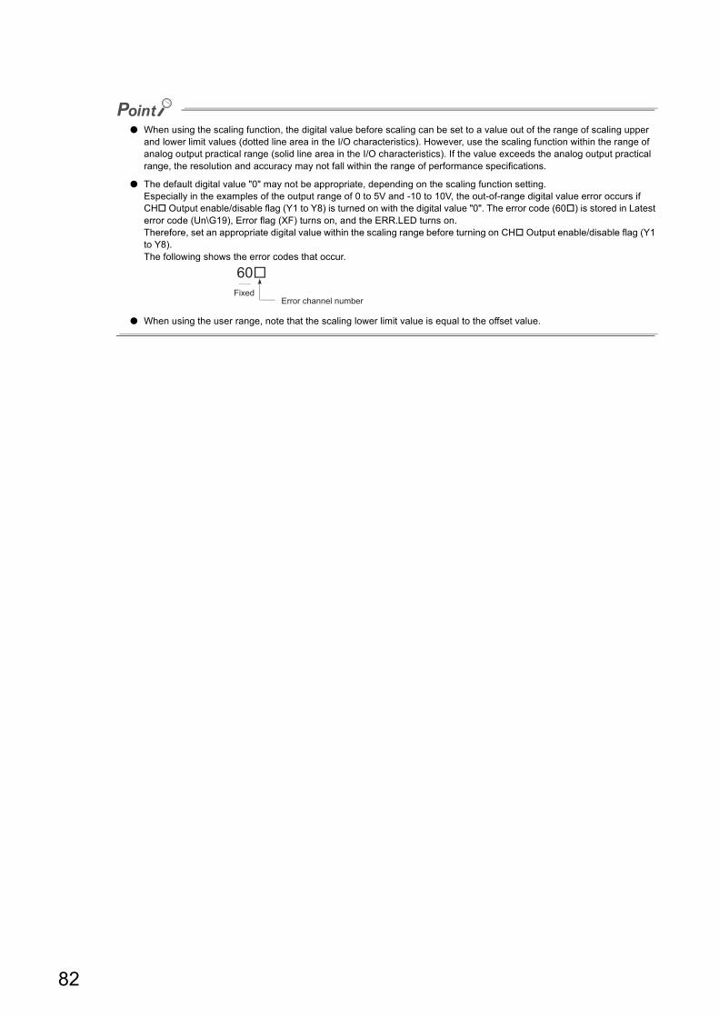
● When using the scaling function, the digital value before scaling can be set to a value out of the range of scaling upper and lower limit values (dotted line area in the I/O characteristics). However, use the scaling function within the range of analog output practical range (solid line area in the I/O characteristics). If the value exceeds the analog output practical range, the resolution and accuracy may not fall within the range of performance specifications.
● The default digital value "0" may not be appropriate, depending on the scaling function setting.Especially in the examples of the output range of 0 to 5V and -10 to 10V, the out-of-range digital value error occurs if CH Output enable/disable flag (Y1 to Y8) is turned on with the digital value "0". The error code (60) is stored in Latest error code (Un\G19), Error flag (XF) turns on, and the ERR.LED turns on.Therefore, set an appropriate digital value within the scaling range before turning on CH Output enable/disable flag (Y1 to Y8).The following shows the error codes that occur.
● When using the user range, note that the scaling lower limit value is equal to the offset value.
60
Error channel numberFixed
82
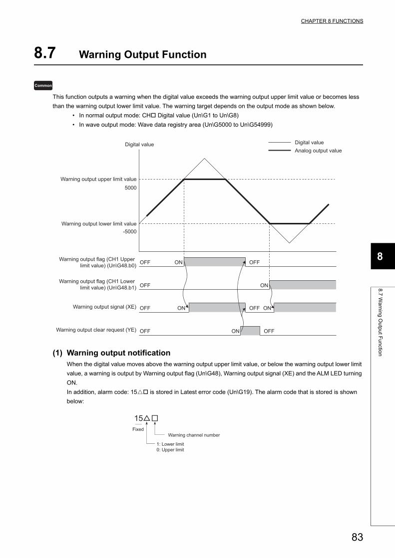
CHAPTER 8 FUNCTIONS
8
8.7
Wa
rnin
g O
utp
ut F
un
ction
8.7 Warning Output Function
This function outputs a warning when the digital value exceeds the warning output upper limit value or becomes less
than the warning output lower limit value. The warning target depends on the output mode as shown below.
• In normal output mode: CH Digital value (Un\G1 to Un\G8)
• In wave output mode: Wave data registry area (Un\G5000 to Un\G54999)
(1) Warning output notificationWhen the digital value moves above the warning output upper limit value, or below the warning output lower limit
value, a warning is output by Warning output flag (Un\G48), Warning output signal (XE) and the ALM LED turning
ON.
In addition, alarm code: 15 is stored in Latest error code (Un\G19). The alarm code that is stored is shown
below:
Common
Warning output upper limit value
OFF ON
Warning output signal (XE) OFF
OFF ON
Warning output lower limit value
5000
-5000
Digital value
Warning output flag (CH1 Upper limit value) (Un\G48.b0)
Warning output flag (CH1 Lower limit value) (Un\G48.b1)
Warning output clear request (YE) OFF
Digital valueAnalog output value
ON ON
ON OFF
OFF
OFF
15
Warning channel number
Fixed
1: Lower limit
0: Upper limit
83
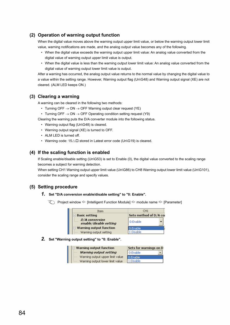
(2) Operation of warning output functionWhen the digital value moves above the warning output upper limit value, or below the warning output lower limit
value, warning notifications are made, and the analog output value becomes any of the following.
• When the digital value exceeds the warning output upper limit value: An analog value converted from the
digital value of warning output upper limit value is output.
• When the digital value is less than the warning output lower limit value: An analog value converted from the
digital value of warning output lower limit value is output.
After a warning has occurred, the analog output value returns to the normal value by changing the digital value to
a value within the setting range. However, Warning output flag (Un\G48) and Warning output signal (XE) are not
cleared. (ALM LED keeps ON.)
(3) Clearing a warningA warning can be cleared in the following two methods:
• Turning OFF ON OFF Warning output clear request (YE)
• Turning OFF ON OFF Operating condition setting request (Y9)
Clearing the warning puts the D/A converter module into the following status.
• Warning output flag (Un\G48) is cleared.
• Warning output signal (XE) is turned to OFF.
• ALM LED is turned off.
• Warning code: 15 stored in Latest error code (Un\G19) is cleared.
(4) If the scaling function is enabledIf Scaling enable/disable setting (Un\G53) is set to Enable (0), the digital value converted to the scaling range
becomes a subject for warning detection.
When setting CH1 Warning output upper limit value (Un\G86) to CH8 Warning output lower limit value (Un\G101),
consider the scaling range and specify values.
(5) Setting procedure
1. Set "D/A conversion enable/disable setting" to "0: Enable".
Project window [Intelligent Function Module] module name [Parameter]
2. Set "Warning output setting" to "0: Enable".
84
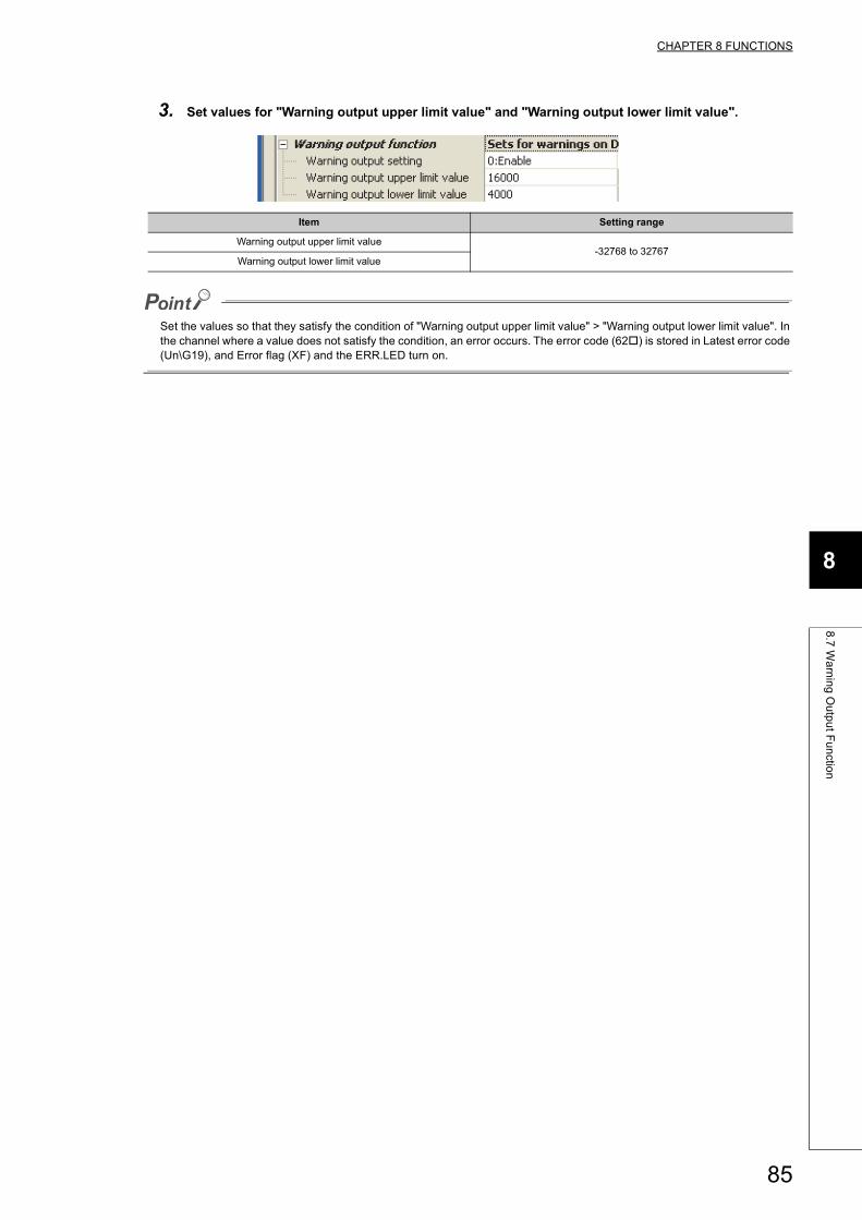
CHAPTER 8 FUNCTIONS
8
8.7
Wa
rnin
g O
utp
ut F
un
ction
3. Set values for "Warning output upper limit value" and "Warning output lower limit value".
Set the values so that they satisfy the condition of "Warning output upper limit value" > "Warning output lower limit value". In the channel where a value does not satisfy the condition, an error occurs. The error code (62) is stored in Latest error code (Un\G19), and Error flag (XF) and the ERR.LED turn on.
Item Setting range
Warning output upper limit value-32768 to 32767
Warning output lower limit value
85
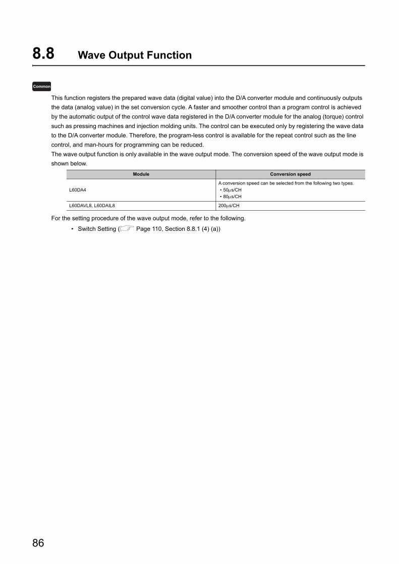
8.8 Wave Output Function
This function registers the prepared wave data (digital value) into the D/A converter module and continuously outputs
the data (analog value) in the set conversion cycle. A faster and smoother control than a program control is achieved
by the automatic output of the control wave data registered in the D/A converter module for the analog (torque) control
such as pressing machines and injection molding units. The control can be executed only by registering the wave data
to the D/A converter module. Therefore, the program-less control is available for the repeat control such as the line
control, and man-hours for programming can be reduced.
The wave output function is only available in the wave output mode. The conversion speed of the wave output mode is
shown below.
For the setting procedure of the wave output mode, refer to the following.
• Switch Setting ( Page 110, Section 8.8.1 (4) (a))
Module Conversion speed
L60DA4
A conversion speed can be selected from the following two types.
• 50s/CH
• 80s/CH
L60DAVL8, L60DAIL8 200s/CH
Common
86
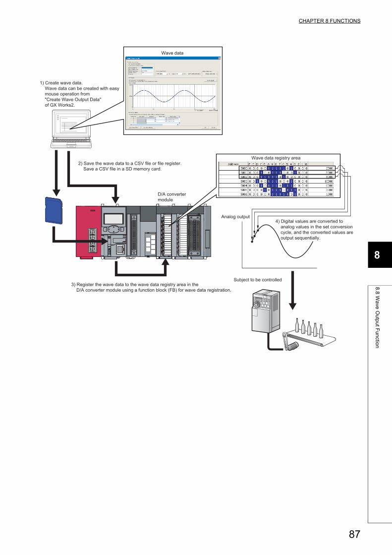
CHAPTER 8 FUNCTIONS
8
8.8
Wa
ve O
utp
ut F
un
ction
2) Save the wave data to a CSV file or file register. Save a CSV file in a SD memory card.
3) Register the wave data to the wave data registry area in the D/A converter module using a function block (FB) for wave data registration.
Subject to be controlled
Analog output4) Digital values are converted to analog values in the set conversion cycle, and the converted values are output sequentially.
1) Create wave data. Wave data can be created with easy mouse operation from "Create Wave Output Data" of GX Works2.
D/A converter module
Wave data
Wave data registry area
87

(1) Wave output function procedureThe following shows how to use the wave output function.
(1) Page 96, Section 8.8.1
(2) Page 96, Section 8.8.1 (1)
(3) Page 103, Section 8.8.1 (2)
(4) Page 106, Section 8.8.1 (3)
(5) Page 110, Section 8.8.1 (4)
(6) Page 113, Section 8.8.2
(7) Page 113, Section 8.8.2 (1)
(8) Page 114, Section 8.8.2 (2)
Setting parameters of the wave output function
Registering the wave data and parameters of the wave output function
Starting/stopping/pausing wave output
Creating wave data
End
Start
Switch setting and basic setting
Initial settings of the wave output function
Execution of the wave output function
Writing data to a file register (ZR) or CSV file
(1)
(2)
(3)
(5)
(6)
(7)
(8)
(4)
88
CHAPTER 8 FUNCTIONS
8
8.8
Wa
ve O
utp
ut F
un
ction
The wave data creation and parameter setting of the wave output function can be executed easily with "Create
Wave Output Data" of GX Works2. These setting contents are saved in the file register (ZR) of the CPU module
or in a CSV file and registered to the buffer memory of the D/A converter module with the function block (FB) for
the wave data registration. For details on the function block (FB) for the wave data registration and wave output
execution, refer to the following manual.
• MELSEC-L Digital-Analog Converter Module FB Library Reference Manual (FBM-M031)
• MELSEC-L Digital-Analog Converter Module FB Library (CC-Link IE Field compatible) Reference
Manual (FBM-M072)
• MELSEC-L Digital-Analog Converter Module FB Library Reference Manual (FBM-M158)
• MELSEC-L Digital-Analog Converter Module FB Library (CC-Link IE Field compatible) Reference
Manual (FBM-M165)
89
(a) Feature of a file register (ZR) and a CSV file concerning wave data storage
• File register (ZR): The wave data and parameter setting contents remain in the CPU module even after
power ON OFF or reset of the CPU module.
• CSV file: The wave data and parameter setting can be used for the D/A converter module of other
programmable controller system only by copying the CSV file.
(2) Parameter settings for the wave output functionSet the parameters of the wave output function to the following buffer memory areas to use the wave output
function. For details on each buffer memory, refer to the following.
• Details of Buffer Memory Addresses ( Page 190, Appendix 2)
For details on the parameter setting, refer to the following.
• Setting parameters of the wave output function ( Page 103, Section 8.8.1 (2))
(3) Restrictions and precautions on the wave output functionThe wave output function has the following restrictions and precautions.
(a) Output range setting
The user range cannot be used. When using the wave output function, select the range other than the user
range. For the setting procedure of the output range, refer to the following.
• Switch Setting ( Page 110, Section 8.8.1 (4) (a))
(b) Analog output HOLD/CLEAR function
In the analog output HOLD/CLEAR function, the operation of the D/A converter module in the wave output
mode differs from the operation in the normal output mode. For details, refer to the following.
• Analog Output HOLD/CLEAR Function ( Page 72, Section 8.4 (1) (b))
(c) Scaling function
The scaling function cannot be used in the wave output mode. When using the wave output function, disable
the scaling function.
Setting item Buffer memory address Reference
Output setting during wave output stop Un\G1008 to Un\G1015 Page 200, Appendix 2 (19)
Output value during wave output stop Un\G1016 to Un\G1023 Page 201, Appendix 2 (20)
Wave pattern start address setting Un\G1024 to Un\G1039 Page 202, Appendix 2 (21)
Wave pattern data points setting Un\G1040 to Un\G1055 Page 203, Appendix 2 (22)
Wave pattern output repetition setting Un\G1056 to Un\G1063 Page 204, Appendix 2 (23)
Constant for wave output conversion cycle Un\G1064 to Un\G1071 Page 204, Appendix 2 (24)
Wave data registry area Un\G5000 to Un\G54999 Page 215, Appendix 2 (43)
90
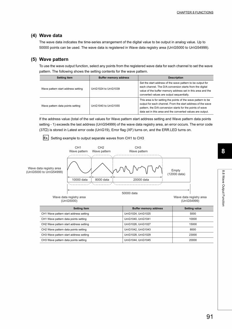
CHAPTER 8 FUNCTIONS
8
8.8
Wa
ve O
utp
ut F
un
ction
(4) Wave dataThe wave data indicates the time-series arrangement of the digital value to be output in analog value. Up to
50000 points can be used. The wave data is registered in Wave data registry area (Un\G5000 to Un\G54999).
(5) Wave patternTo use the wave output function, select any points from the registered wave data for each channel to set the wave
pattern. The following shows the setting contents for the wave pattern.
If the address value (total of the set values for Wave pattern start address setting and Wave pattern data points
setting - 1) exceeds the last address (Un\G54999) of the wave data registry area, an error occurs. The error code
(37) is stored in Latest error code (Un\G19), Error flag (XF) turns on, and the ERR.LED turns on.
Ex. Setting example to output separate waves from CH1 to CH3
Setting item Buffer memory address Description
Wave pattern start address setting Un\G1024 to Un\G1039
Set the start address of the wave pattern to be output for
each channel. The D/A conversion starts from the digital
value of the buffer memory address set in this area and the
converted values are output sequentially.
Wave pattern data points setting Un\G1040 to Un\G1055
This area is for setting the points of the wave pattern to be
output for each channel. From the start address of the wave
pattern, the D/A conversion starts for the points of wave
data set in this area and the converted values are output.
Setting item Buffer memory address Setting value
CH1 Wave pattern start address setting Un\G1024, Un\G1025 5000
CH1 Wave pattern data points setting Un\G1040, Un\G1041 10000
CH2 Wave pattern start address setting Un\G1026, Un\G1027 15000
CH2 Wave pattern data points setting Un\G1042, Un\G1043 8000
CH3 Wave pattern start address setting Un\G1028, Un\G1029 23000
CH3 Wave pattern data points setting Un\G1044, Un\G1045 20000
Empty
(12000 data)
50000 data
8000 data 20000 data10000 data
CH1
Wave pattern
CH2
Wave pattern
CH3
Wave pattern
Wave data registry area
(Un\G5000 to Un\G54999)
Wave data registry area
(Un\G5000)
Wave data registry area
(Un\G54999)
91
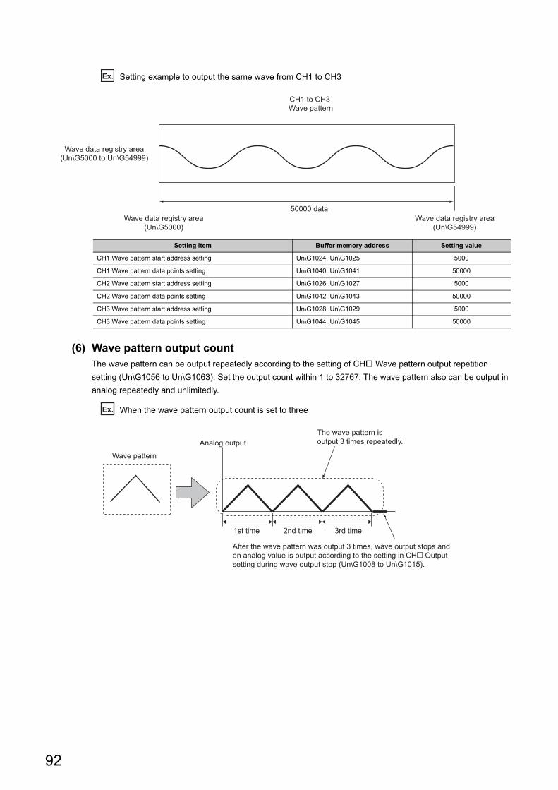
Ex. Setting example to output the same wave from CH1 to CH3
(6) Wave pattern output countThe wave pattern can be output repeatedly according to the setting of CH Wave pattern output repetition
setting (Un\G1056 to Un\G1063). Set the output count within 1 to 32767. The wave pattern also can be output in
analog repeatedly and unlimitedly.
Ex. When the wave pattern output count is set to three
Setting item Buffer memory address Setting value
CH1 Wave pattern start address setting Un\G1024, Un\G1025 5000
CH1 Wave pattern data points setting Un\G1040, Un\G1041 50000
CH2 Wave pattern start address setting Un\G1026, Un\G1027 5000
CH2 Wave pattern data points setting Un\G1042, Un\G1043 50000
CH3 Wave pattern start address setting Un\G1028, Un\G1029 5000
CH3 Wave pattern data points setting Un\G1044, Un\G1045 50000
50000 data
CH1 to CH3
Wave pattern
Wave data registry area
(Un\G5000 to Un\G54999)
Wave data registry area
(Un\G5000)
Wave data registry area
(Un\G54999)
The wave pattern is output 3 times repeatedly.Analog output
Wave pattern
1st time 2nd time 3rd time
After the wave pattern was output 3 times, wave output stops and an analog value is output according to the setting in CH Output setting during wave output stop (Un\G1008 to Un\G1015).
92
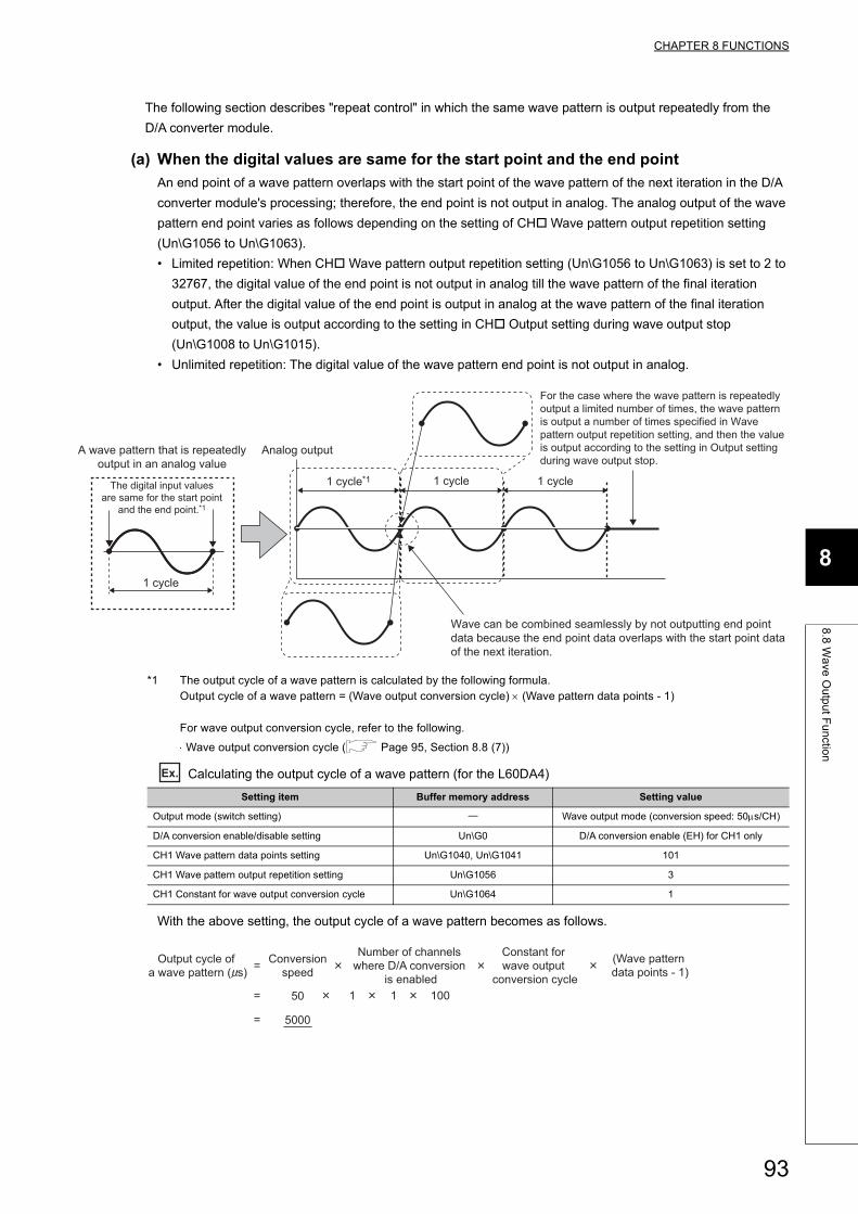
CHAPTER 8 FUNCTIONS
8
8.8
Wa
ve O
utp
ut F
un
ction
The following section describes "repeat control" in which the same wave pattern is output repeatedly from the
D/A converter module.
(a) When the digital values are same for the start point and the end point
An end point of a wave pattern overlaps with the start point of the wave pattern of the next iteration in the D/A
converter module's processing; therefore, the end point is not output in analog. The analog output of the wave
pattern end point varies as follows depending on the setting of CH Wave pattern output repetition setting
(Un\G1056 to Un\G1063).
• Limited repetition: When CH Wave pattern output repetition setting (Un\G1056 to Un\G1063) is set to 2 to
32767, the digital value of the end point is not output in analog till the wave pattern of the final iteration
output. After the digital value of the end point is output in analog at the wave pattern of the final iteration
output, the value is output according to the setting in CH Output setting during wave output stop
(Un\G1008 to Un\G1015).
• Unlimited repetition: The digital value of the wave pattern end point is not output in analog.
*1 The output cycle of a wave pattern is calculated by the following formula.Output cycle of a wave pattern = (Wave output conversion cycle) (Wave pattern data points - 1)
For wave output conversion cycle, refer to the following.
Wave output conversion cycle ( Page 95, Section 8.8 (7))
Ex. Calculating the output cycle of a wave pattern (for the L60DA4)
With the above setting, the output cycle of a wave pattern becomes as follows.
Setting item Buffer memory address Setting value
Output mode (switch setting) Wave output mode (conversion speed: 50s/CH)
D/A conversion enable/disable setting Un\G0 D/A conversion enable (EH) for CH1 only
CH1 Wave pattern data points setting Un\G1040, Un\G1041 101
CH1 Wave pattern output repetition setting Un\G1056 3
CH1 Constant for wave output conversion cycle Un\G1064 1
Wave can be combined seamlessly by not outputting end pointdata because the end point data overlaps with the start point dataof the next iteration.
A wave pattern that is repeatedlyoutput in an analog value
The digital input valuesare same for the start point
and the end point.*1
For the case where the wave pattern is repeatedlyoutput a limited number of times, the wave patternis output a number of times specified in Wavepattern output repetition setting, and then the valueis output according to the setting in Output settingduring wave output stop.
Analog output
1 cycle*1 1 cycle 1 cycle
1 cycle
Output cycle of
a wave pattern ( s)
Conversion
speed=
Number of channels
where D/A conversion
is enabled
Constant for
wave output
conversion cycle
(Wave pattern
data points - 1)
50= 1 1 100
5000=
93
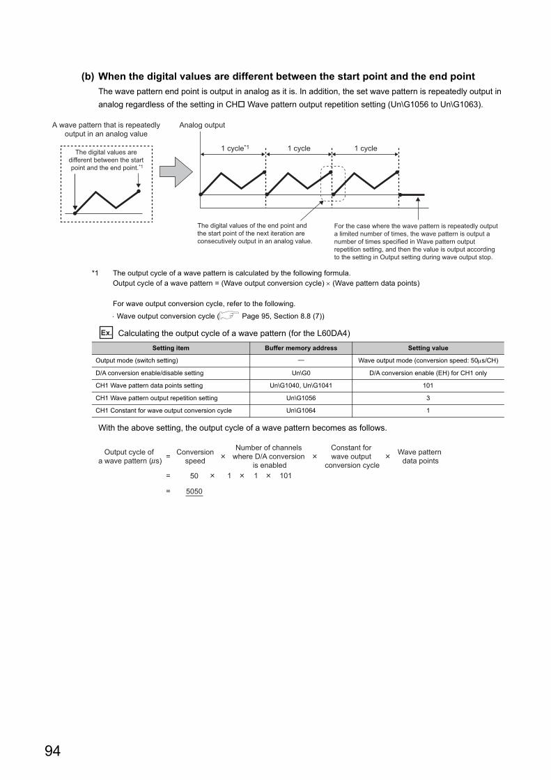
(b) When the digital values are different between the start point and the end point
The wave pattern end point is output in analog as it is. In addition, the set wave pattern is repeatedly output in
analog regardless of the setting in CH Wave pattern output repetition setting (Un\G1056 to Un\G1063).
*1 The output cycle of a wave pattern is calculated by the following formula.Output cycle of a wave pattern = (Wave output conversion cycle) (Wave pattern data points)
For wave output conversion cycle, refer to the following.
Wave output conversion cycle ( Page 95, Section 8.8 (7))
Ex. Calculating the output cycle of a wave pattern (for the L60DA4)
With the above setting, the output cycle of a wave pattern becomes as follows.
Setting item Buffer memory address Setting value
Output mode (switch setting) Wave output mode (conversion speed: 50s/CH)
D/A conversion enable/disable setting Un\G0 D/A conversion enable (EH) for CH1 only
CH1 Wave pattern data points setting Un\G1040, Un\G1041 101
CH1 Wave pattern output repetition setting Un\G1056 3
CH1 Constant for wave output conversion cycle Un\G1064 1
A wave pattern that is repeatedlyoutput in an analog value
For the case where the wave pattern is repeatedly outputa limited number of times, the wave pattern is output anumber of times specified in Wave pattern outputrepetition setting, and then the value is output accordingto the setting in Output setting during wave output stop.
Analog output
1 cycle*1 1 cycle 1 cycle
The digital values of the end point andthe start point of the next iteration areconsecutively output in an analog value.
The digital values are different between the start point and the end point.*1
Conversion
speed=
Number of channels
where D/A conversion
is enabled
Constant for
wave output
conversion cycle
Wave pattern
data points
50= 1 1 101
5050=
Output cycle of
a wave pattern ( s)
94
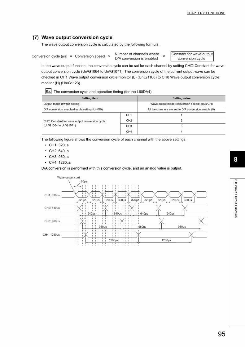
CHAPTER 8 FUNCTIONS
8
8.8
Wa
ve O
utp
ut F
un
ction
(7) Wave output conversion cycleThe wave output conversion cycle is calculated by the following formula.
In the wave output function, the conversion cycle can be set for each channel by setting CH Constant for wave
output conversion cycle (Un\G1064 to Un\G1071). The conversion cycle of the current output wave can be
checked in CH1 Wave output conversion cycle monitor (L) (Un\G1108) to CH8 Wave output conversion cycle
monitor (H) (Un\G1123).
Ex. The conversion cycle and operation timing (for the L60DA4)
The following figure shows the conversion cycle of each channel with the above settings.
• CH1: 320s
• CH2: 640s
• CH3: 960s
• CH4: 1280s
D/A conversion is performed with this conversion cycle, and an analog value is output.
Setting item Setting value
Output mode (switch setting) Wave output mode (conversion speed: 80s/CH)
D/A conversion enable/disable setting (Un\G0) All the channels are set to D/A conversion enable (0).
CH Constant for wave output conversion cycle
(Un\G1064 to Un\G1071)
CH1 1
CH2 2
CH3 3
CH4 4
Conversion cycle ( s) Conversion speed = Number of channels whereD/A conversion is enabled
Constant for wave outputconversion cycle
Wave output start
CH2: 640μs
CH3: 960μs
CH4: 1280μs
CH1: 320μs320μs
80μs
640μs 640μs 640μs 640μs
320μs 320μs 320μs 320μs 320μs 320μs 320μs 320μs
960μs
1280μs 1280μs
960μs 960μs
95
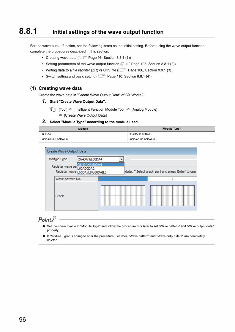
8.8.1 Initial settings of the wave output function
For the wave output function, set the following items as the initial setting. Before using the wave output function,
complete the procedures described in this section.
• Creating wave data ( Page 96, Section 8.8.1 (1))
• Setting parameters of the wave output function ( Page 103, Section 8.8.1 (2))
• Writing data to a file register (ZR) or CSV file ( Page 106, Section 8.8.1 (3))
• Switch setting and basic setting ( Page 110, Section 8.8.1 (4))
(1) Creating wave dataCreate the wave data in "Create Wave Output Data" of GX Works2.
1. Start "Create Wave Output Data".
[Tool] [Intelligent Function Module Tool] [Analog Module]
[Create Wave Output Data]
2. Select "Module Type" according to the module used.
● Set the correct value in "Module Type" and follow the procedure 3 or later to set "Wave pattern" and "Wave output data" properly.
● If "Module Type" is changed after the procedure 3 or later, "Wave pattern" and "Wave output data" are completely deleted.
Module "Module Type"
L60DA4 Q64DAH/L60DA4
L60DAVL8, L60DAIL8 L60DAVL8/L60DAIL8
96
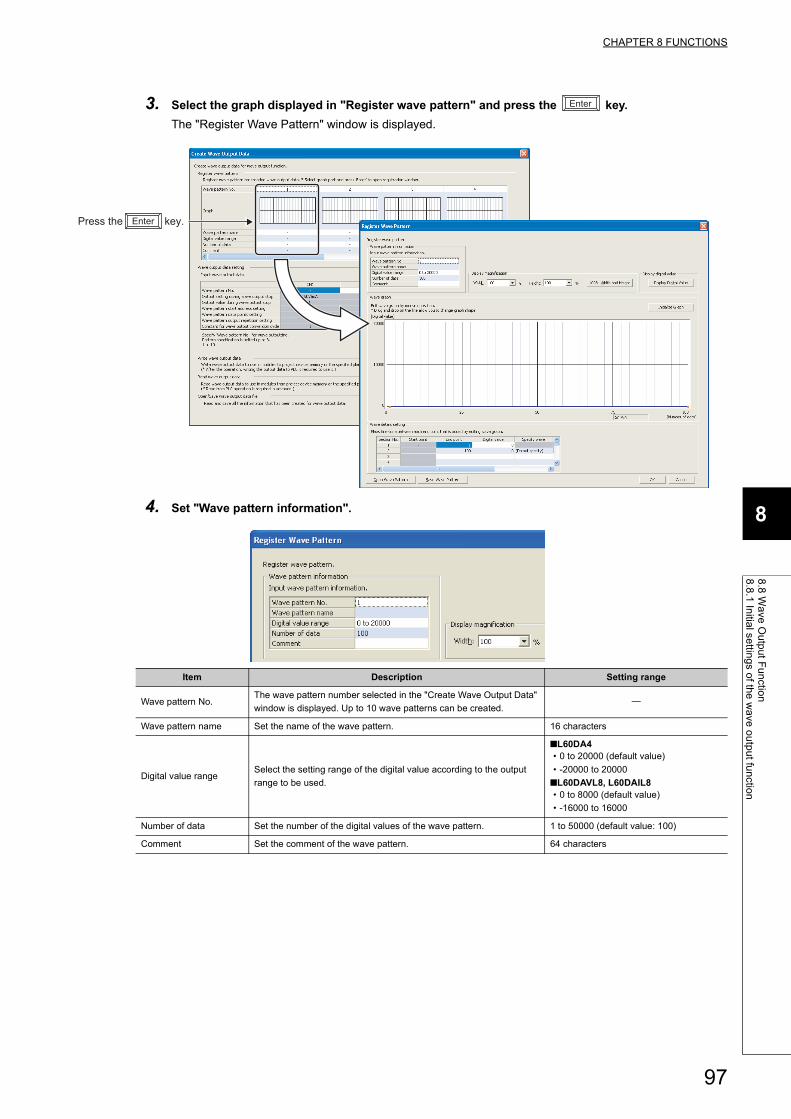
CHAPTER 8 FUNCTIONS
8
8.8
Wa
ve O
utp
ut F
un
ction
8.8
.1 In
itial se
tting
s of th
e w
ave
ou
tpu
t fun
ction
3. Select the graph displayed in "Register wave pattern" and press the key.
The "Register Wave Pattern" window is displayed.
4. Set "Wave pattern information".
Item Description Setting range
Wave pattern No.The wave pattern number selected in the "Create Wave Output Data"
window is displayed. Up to 10 wave patterns can be created.
Wave pattern name Set the name of the wave pattern. 16 characters
Digital value rangeSelect the setting range of the digital value according to the output
range to be used.
■L60DA4• 0 to 20000 (default value)
• -20000 to 20000
■L60DAVL8, L60DAIL8• 0 to 8000 (default value)
• -16000 to 16000
Number of data Set the number of the digital values of the wave pattern. 1 to 50000 (default value: 100)
Comment Set the comment of the wave pattern. 64 characters
Enter
EnterPress the key.
97
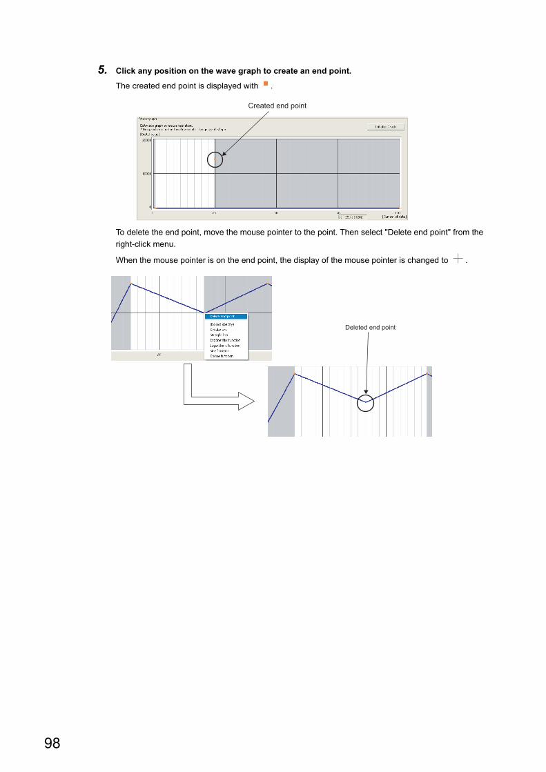
5. Click any position on the wave graph to create an end point.
The created end point is displayed with .
To delete the end point, move the mouse pointer to the point. Then select "Delete end point" from the
right-click menu.
When the mouse pointer is on the end point, the display of the mouse pointer is changed to .
Created end point
Deleted end point
98
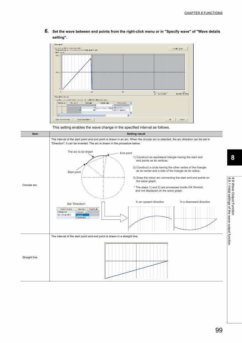
CHAPTER 8 FUNCTIONS
8
8.8
Wa
ve O
utp
ut F
un
ction
8.8
.1 In
itial se
tting
s of th
e w
ave
ou
tpu
t fun
ction
6. Set the wave between end points from the right-click menu or in "Specify wave" of "Wave details
setting".
This setting enables the wave change in the specified interval as follows.
Item Setting result
Circular arc
The interval of the start point and end point is drawn in an arc. When the circular arc is selected, the arc direction can be set in
"Direction"; it can be inverted. The arc is drawn in the procedure below.
Straight line
The interval of the start point and end point is drawn in a straight line.
Start point
End point
Set "Direction".In an upward direction In a downward direction
The arc to be drawn
1) Construct an equilateral triangle having the start and end points as its vertices.
2) Construct a circle having the other vertex of the triangle as its center and a side of the triangle as its radius.
3) Draw the minor arc connecting the start and end points on the wave graph.
* The steps 1) and 2) are processed inside GX Works2, and not displayed on the wave graph.
99
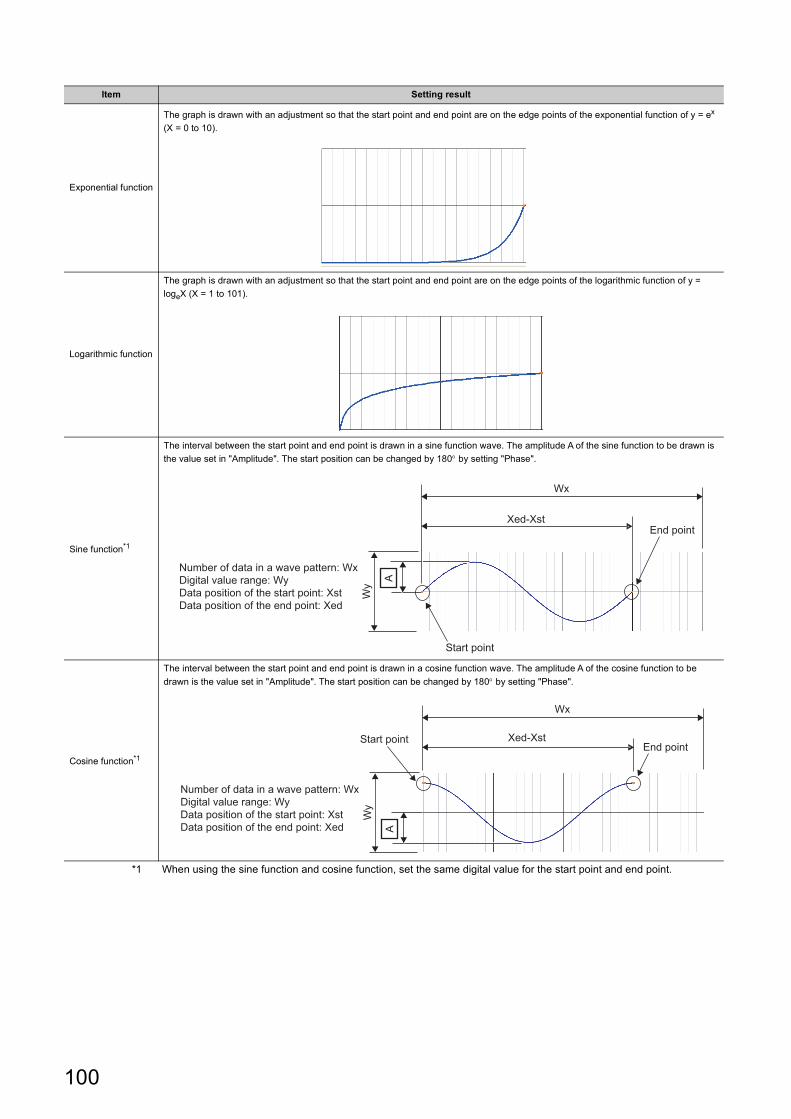
*1 When using the sine function and cosine function, set the same digital value for the start point and end point.
Exponential function
The graph is drawn with an adjustment so that the start point and end point are on the edge points of the exponential function of y = ex
(X = 0 to 10).
Logarithmic function
The graph is drawn with an adjustment so that the start point and end point are on the edge points of the logarithmic function of y =
logeX (X = 1 to 101).
Sine function*1
The interval between the start point and end point is drawn in a sine function wave. The amplitude A of the sine function to be drawn is
the value set in "Amplitude". The start position can be changed by 180 by setting "Phase".
Cosine function*1
The interval between the start point and end point is drawn in a cosine function wave. The amplitude A of the cosine function to be
drawn is the value set in "Amplitude". The start position can be changed by 180 by setting "Phase".
Item Setting result
A
Wx
Wy
Number of data in a wave pattern: Wx
Digital value range: Wy
Data position of the start point: Xst
Data position of the end point: Xed
Start point
End pointXed-Xst
A
Wx
Wy
Number of data in a wave pattern: Wx
Digital value range: Wy
Data position of the start point: Xst
Data position of the end point: Xed
Start pointEnd point
Xed-Xst
100
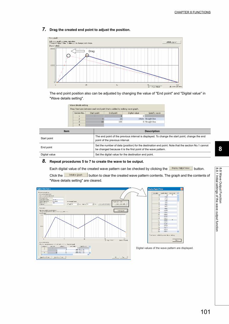
CHAPTER 8 FUNCTIONS
8
8.8
Wa
ve O
utp
ut F
un
ction
8.8
.1 In
itial se
tting
s of th
e w
ave
ou
tpu
t fun
ction
7. Drag the created end point to adjust the position.
The end point position also can be adjusted by changing the value of "End point" and "Digital value" in
"Wave details setting".
8. Repeat procedures 5 to 7 to create the wave to be output.
Each digital value of the created wave pattern can be checked by clicking the button.
Click the button to clear the created wave pattern contents. The graph and the contents of
"Wave details setting" are cleared.
Item Description
Start pointThe end point of the previous interval is displayed. To change the start point, change the end
point of the previous interval.
End pointSet the number of data (position) for the destination end point. Note that the section No.1 cannot
be changed because it is the first point of the wave pattern.
Digital value Set the digital value for the destination end point.
Drag
Digital values of the wave pattern are displayed.
101
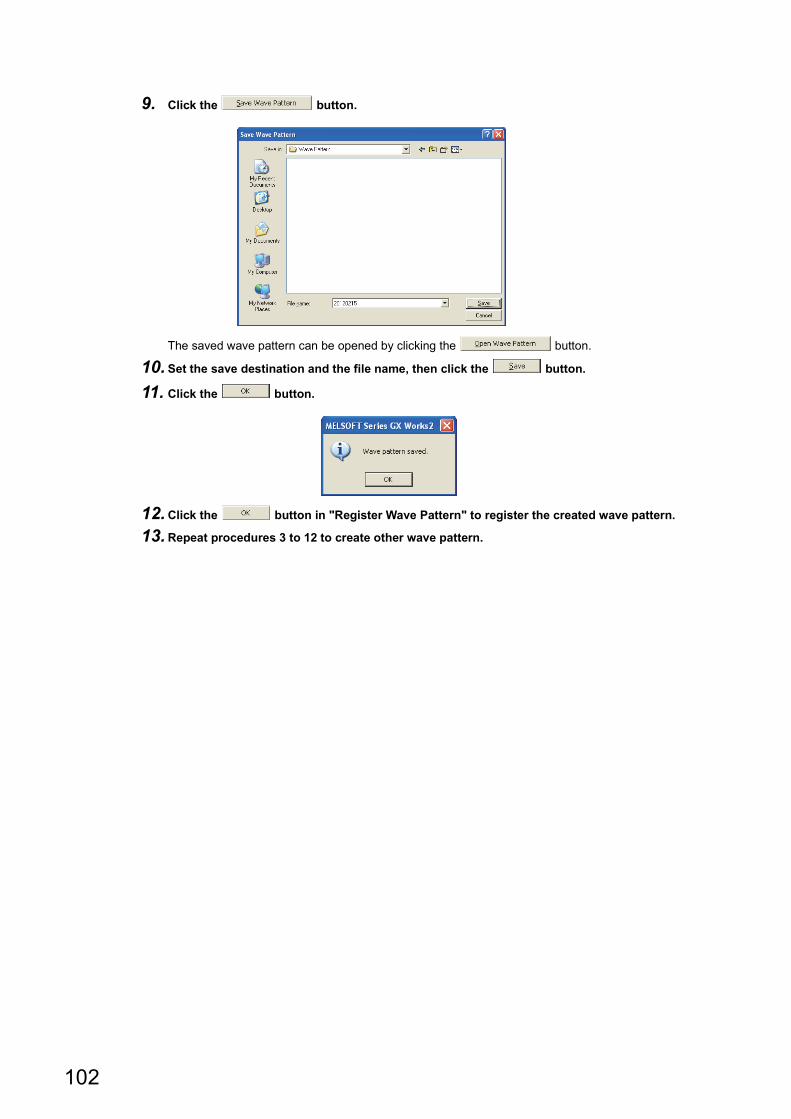
9. Click the button.
The saved wave pattern can be opened by clicking the button.
10. Set the save destination and the file name, then click the button.
11. Click the button.
12.Click the button in "Register Wave Pattern" to register the created wave pattern.
13.Repeat procedures 3 to 12 to create other wave pattern.
102
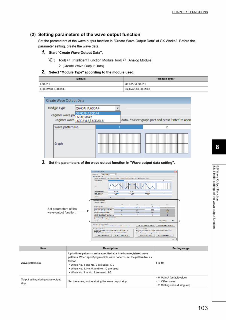
CHAPTER 8 FUNCTIONS
8
8.8
Wa
ve O
utp
ut F
un
ction
8.8
.1 In
itial se
tting
s of th
e w
ave
ou
tpu
t fun
ction
(2) Setting parameters of the wave output functionSet the parameters of the wave output function in "Create Wave Output Data" of GX Works2. Before the
parameter setting, create the wave data.
1. Start "Create Wave Output Data".
[Tool] [Intelligent Function Module Tool] [Analog Module]
[Create Wave Output Data]
2. Select "Module Type" according to the module used.
3. Set the parameters of the wave output function in "Wave output data setting".
Module "Module Type"
L60DA4 Q64DAH/L60DA4
L60DAVL8, L60DAIL8 L60DAVL8/L60DAIL8
Item Description Setting range
Wave pattern No.
Up to three patterns can be specified at a time from registered wave
patterns. When specifying multiple wave patterns, set the pattern No. as
follows.
• When No. 1 and No. 2 are used: 1, 2
• When No. 1, No. 5, and No. 10 are used:
• When No. 1 to No. 3 are used: 1-3
1 to 10
Output setting during wave output
stopSet the analog output during the wave output stop.
• 0: 0V/mA (default value)
• 1: Offset value
• 2: Setting value during stop
Set parameters of thewave output function.
103
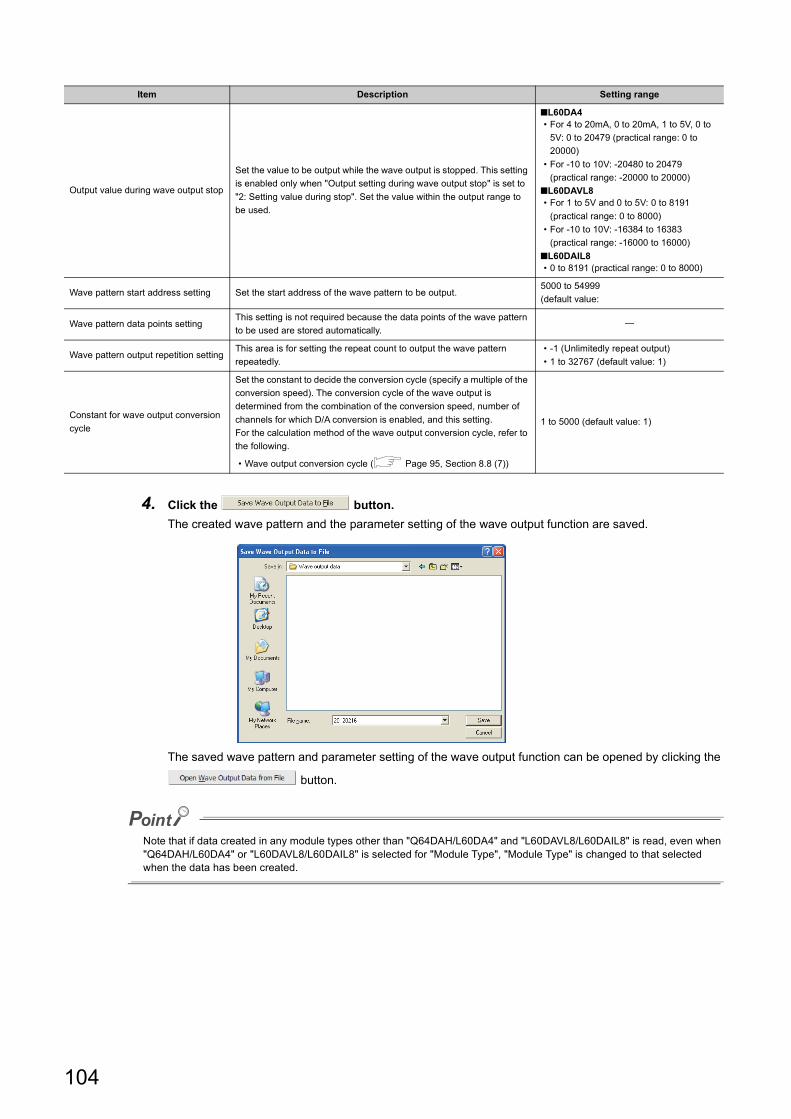
4. Click the button.
The created wave pattern and the parameter setting of the wave output function are saved.
The saved wave pattern and parameter setting of the wave output function can be opened by clicking the
button.
Note that if data created in any module types other than "Q64DAH/L60DA4" and "L60DAVL8/L60DAIL8" is read, even when "Q64DAH/L60DA4" or "L60DAVL8/L60DAIL8" is selected for "Module Type", "Module Type" is changed to that selected when the data has been created.
Output value during wave output stop
Set the value to be output while the wave output is stopped. This setting
is enabled only when "Output setting during wave output stop" is set to
"2: Setting value during stop". Set the value within the output range to
be used.
■L60DA4• For 4 to 20mA, 0 to 20mA, 1 to 5V, 0 to
5V: 0 to 20479 (practical range: 0 to
20000)
• For -10 to 10V: -20480 to 20479
(practical range: -20000 to 20000)
■L60DAVL8• For 1 to 5V and 0 to 5V: 0 to 8191
(practical range: 0 to 8000)
• For -10 to 10V: -16384 to 16383
(practical range: -16000 to 16000)
■L60DAIL8• 0 to 8191 (practical range: 0 to 8000)
Wave pattern start address setting Set the start address of the wave pattern to be output.5000 to 54999
(default value:
Wave pattern data points settingThis setting is not required because the data points of the wave pattern
to be used are stored automatically.
Wave pattern output repetition settingThis area is for setting the repeat count to output the wave pattern
repeatedly.
• -1 (Unlimitedly repeat output)
• 1 to 32767 (default value: 1)
Constant for wave output conversion
cycle
Set the constant to decide the conversion cycle (specify a multiple of the
conversion speed). The conversion cycle of the wave output is
determined from the combination of the conversion speed, number of
channels for which D/A conversion is enabled, and this setting.
For the calculation method of the wave output conversion cycle, refer to
the following.
• Wave output conversion cycle ( Page 95, Section 8.8 (7))
1 to 5000 (default value: 1)
Item Description Setting range
104
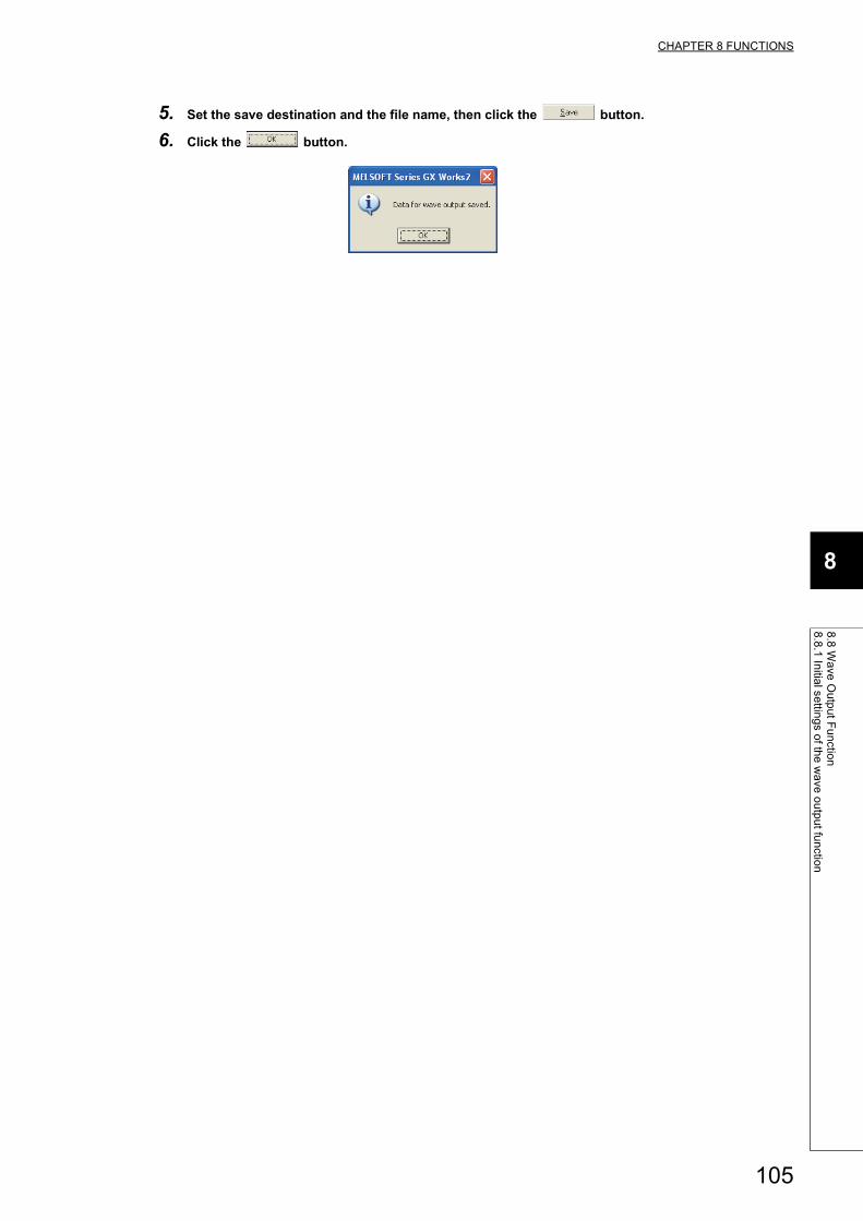
CHAPTER 8 FUNCTIONS
8
8.8
Wa
ve O
utp
ut F
un
ction
8.8
.1 In
itial se
tting
s of th
e w
ave
ou
tpu
t fun
ction
5. Set the save destination and the file name, then click the button.
6. Click the button.
105
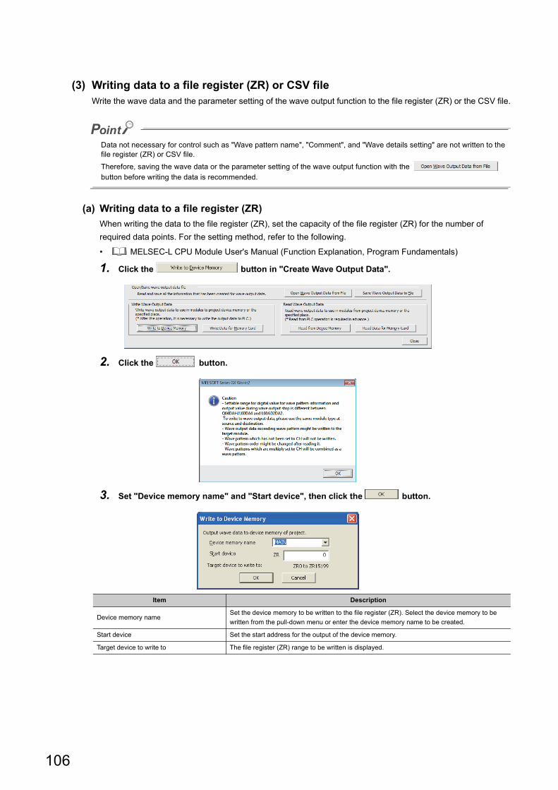
(3) Writing data to a file register (ZR) or CSV fileWrite the wave data and the parameter setting of the wave output function to the file register (ZR) or the CSV file.
Data not necessary for control such as "Wave pattern name", "Comment", and "Wave details setting" are not written to the file register (ZR) or CSV file.
Therefore, saving the wave data or the parameter setting of the wave output function with the
button before writing the data is recommended.
(a) Writing data to a file register (ZR)
When writing the data to the file register (ZR), set the capacity of the file register (ZR) for the number of
required data points. For the setting method, refer to the following.
• MELSEC-L CPU Module User's Manual (Function Explanation, Program Fundamentals)
1. Click the button in "Create Wave Output Data".
2. Click the button.
3. Set "Device memory name" and "Start device", then click the button.
Item Description
Device memory nameSet the device memory to be written to the file register (ZR). Select the device memory to be
written from the pull-down menu or enter the device memory name to be created.
Start device Set the start address for the output of the device memory.
Target device to write to The file register (ZR) range to be written is displayed.
106
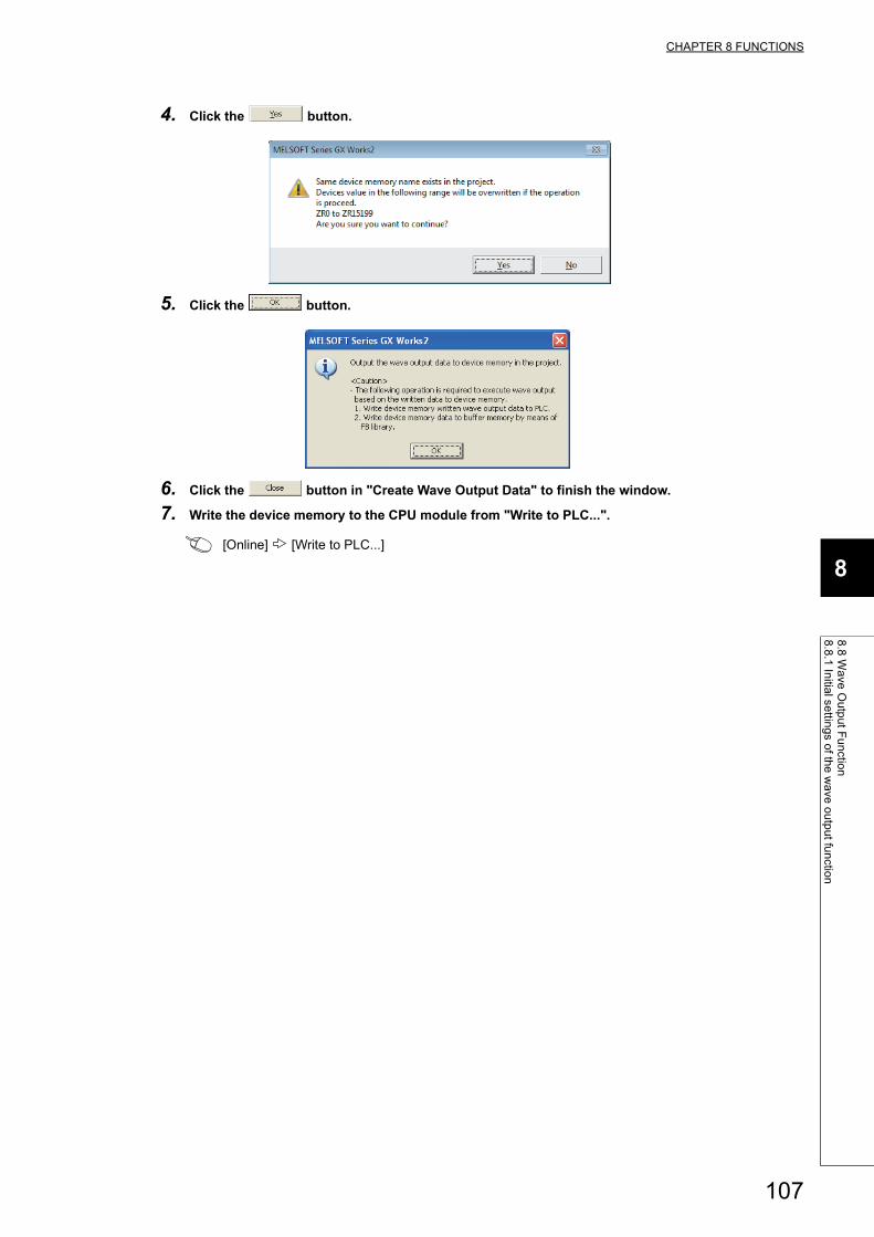
CHAPTER 8 FUNCTIONS
8
8.8
Wa
ve O
utp
ut F
un
ction
8.8
.1 In
itial se
tting
s of th
e w
ave
ou
tpu
t fun
ction
4. Click the button.
5. Click the button.
6. Click the button in "Create Wave Output Data" to finish the window.
7. Write the device memory to the CPU module from "Write to PLC...".
[Online] [Write to PLC...]
107
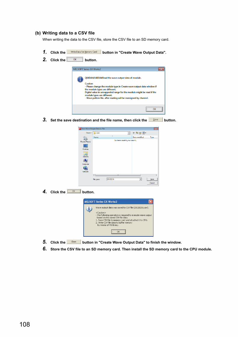
(b) Writing data to a CSV file
When writing the data to the CSV file, store the CSV file to an SD memory card.
1. Click the button in "Create Wave Output Data".
2. Click the button.
3. Set the save destination and the file name, then click the button.
4. Click the button.
5. Click the button in "Create Wave Output Data" to finish the window.
6. Store the CSV file to an SD memory card. Then install the SD memory card to the CPU module.
108
CHAPTER 8 FUNCTIONS
8
8.8
Wa
ve O
utp
ut F
un
ction
8.8
.1 In
itial se
tting
s of th
e w
ave
ou
tpu
t fun
ction
Some oscilloscopes or pulse generators can output the input wave or output wave to the CSV file. To output the wave with the wave output function by using the CSV file data, convert the data format into the one described in the following manual. In addition, convert the fractional value into the integer because the fractional value is unavailable in the wave output function.
• MELSEC-L Digital-Analog Converter Module FB Library Reference Manual (FBM-M031)
• MELSEC-L Digital-Analog Converter Module FB Library (CC-Link IE Field compatible) Reference Manual (FBM-M072)
• MELSEC-L Digital-Analog Converter Module FB Library Reference Manual (FBM-M158)
• MELSEC-L Digital-Analog Converter Module FB Library (CC-Link IE Field compatible) Reference Manual (FBM-M165)
109
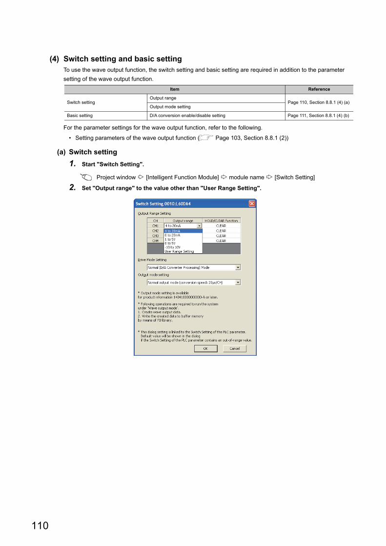
(4) Switch setting and basic settingTo use the wave output function, the switch setting and basic setting are required in addition to the parameter
setting of the wave output function.
For the parameter settings for the wave output function, refer to the following.
• Setting parameters of the wave output function ( Page 103, Section 8.8.1 (2))
(a) Switch setting
1. Start "Switch Setting".
Project window [Intelligent Function Module] module name [Switch Setting]
2. Set "Output range" to the value other than "User Range Setting".
Item Reference
Switch settingOutput range
Page 110, Section 8.8.1 (4) (a)Output mode setting
Basic setting D/A conversion enable/disable setting Page 111, Section 8.8.1 (4) (b)
110
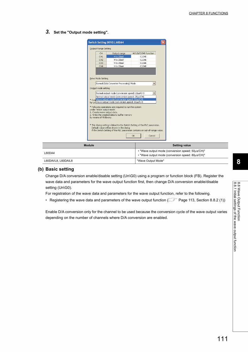
CHAPTER 8 FUNCTIONS
8
8.8
Wa
ve O
utp
ut F
un
ction
8.8
.1 In
itial se
tting
s of th
e w
ave
ou
tpu
t fun
ction
3. Set the "Output mode setting".
(b) Basic setting
Change D/A conversion enable/disable setting (Un\G0) using a program or function block (FB). Register the
wave data and parameters for the wave output function first, then change D/A conversion enable/disable
setting (Un\G0).
For registration of the wave data and parameters for the wave output function, refer to the following.
• Registering the wave data and parameters of the wave output function ( Page 113, Section 8.8.2 (1))
Enable D/A conversion only for the channel to be used because the conversion cycle of the wave output varies
depending on the number of channels where D/A conversion are enabled.
Module Setting value
L60DA4• "Wave output mode (conversion speed: 50s/CH)"
• "Wave output mode (conversion speed: 80s/CH)"
L60DAVL8, L60DAIL8 "Wave Output Mode"
111
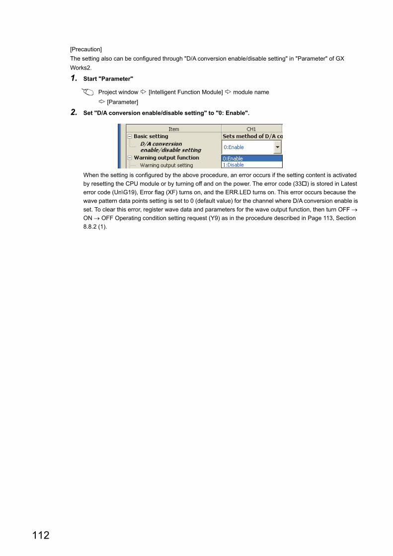
[Precaution]
The setting also can be configured through "D/A conversion enable/disable setting" in "Parameter" of GX
Works2.
1. Start "Parameter"
Project window [Intelligent Function Module] module name
[Parameter]
2. Set "D/A conversion enable/disable setting" to "0: Enable".
When the setting is configured by the above procedure, an error occurs if the setting content is activated
by resetting the CPU module or by turning off and on the power. The error code (33) is stored in Latest
error code (Un\G19), Error flag (XF) turns on, and the ERR.LED turns on. This error occurs because the
wave pattern data points setting is set to 0 (default value) for the channel where D/A conversion enable is
set. To clear this error, register wave data and parameters for the wave output function, then turn OFF
ON OFF Operating condition setting request (Y9) as in the procedure described in Page 113, Section
8.8.2 (1).
112
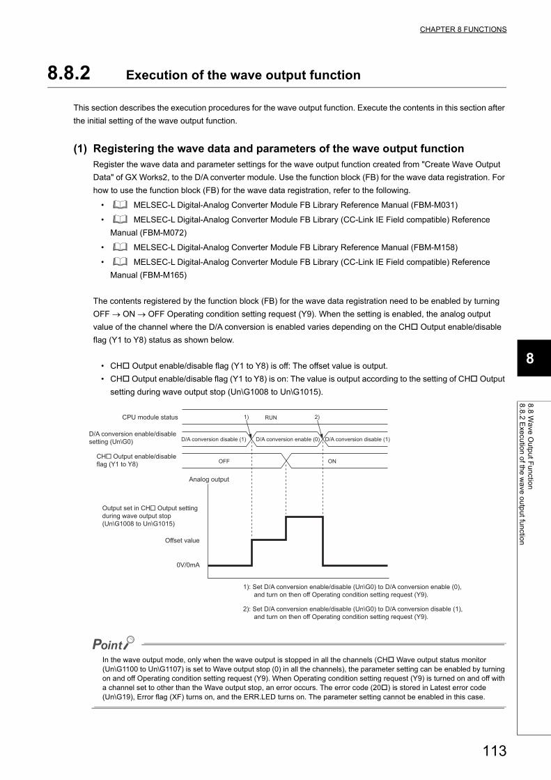
CHAPTER 8 FUNCTIONS
8
8.8
Wa
ve O
utp
ut F
un
ction
8.8
.2 E
xecu
tion
of th
e w
ave
ou
tpu
t fun
ction
8.8.2 Execution of the wave output function
This section describes the execution procedures for the wave output function. Execute the contents in this section after
the initial setting of the wave output function.
(1) Registering the wave data and parameters of the wave output functionRegister the wave data and parameter settings for the wave output function created from "Create Wave Output
Data" of GX Works2, to the D/A converter module. Use the function block (FB) for the wave data registration. For
how to use the function block (FB) for the wave data registration, refer to the following.
• MELSEC-L Digital-Analog Converter Module FB Library Reference Manual (FBM-M031)
• MELSEC-L Digital-Analog Converter Module FB Library (CC-Link IE Field compatible) Reference
Manual (FBM-M072)
• MELSEC-L Digital-Analog Converter Module FB Library Reference Manual (FBM-M158)
• MELSEC-L Digital-Analog Converter Module FB Library (CC-Link IE Field compatible) Reference
Manual (FBM-M165)
The contents registered by the function block (FB) for the wave data registration need to be enabled by turning
OFF ON OFF Operating condition setting request (Y9). When the setting is enabled, the analog output
value of the channel where the D/A conversion is enabled varies depending on the CH Output enable/disable
flag (Y1 to Y8) status as shown below.
• CH Output enable/disable flag (Y1 to Y8) is off: The offset value is output.
• CH Output enable/disable flag (Y1 to Y8) is on: The value is output according to the setting of CH Output
setting during wave output stop (Un\G1008 to Un\G1015).
In the wave output mode, only when the wave output is stopped in all the channels (CH Wave output status monitor (Un\G1100 to Un\G1107) is set to Wave output stop (0) in all the channels), the parameter setting can be enabled by turning on and off Operating condition setting request (Y9). When Operating condition setting request (Y9) is turned on and off with a channel set to other than the Wave output stop, an error occurs. The error code (20) is stored in Latest error code (Un\G19), Error flag (XF) turns on, and the ERR.LED turns on. The parameter setting cannot be enabled in this case.
D/A conversion enable/disable setting (Un\G0)
CPU module status
CH Output enable/disable flag (Y1 to Y8) OFF ON
D/A conversion disable (1) D/A conversion disable (1)D/A conversion enable (0)
RUN
Analog output
Offset value
0V/0mA
Output set in CH Output setting during wave output stop (Un\G1008 to Un\G1015)
1): Set D/A conversion enable/disable (Un\G0) to D/A conversion enable (0), and turn on then off Operating condition setting request (Y9).
2): Set D/A conversion enable/disable (Un\G0) to D/A conversion disable (1), and turn on then off Operating condition setting request (Y9).
1) 2)
113
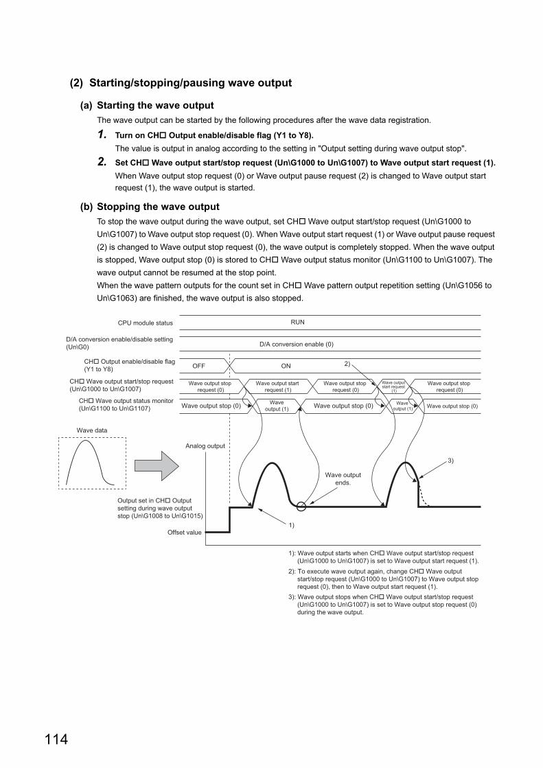
(2) Starting/stopping/pausing wave output
(a) Starting the wave output
The wave output can be started by the following procedures after the wave data registration.
1. Turn on CH Output enable/disable flag (Y1 to Y8).
The value is output in analog according to the setting in "Output setting during wave output stop".
2. Set CH Wave output start/stop request (Un\G1000 to Un\G1007) to Wave output start request (1).
When Wave output stop request (0) or Wave output pause request (2) is changed to Wave output start
request (1), the wave output is started.
(b) Stopping the wave output
To stop the wave output during the wave output, set CH Wave output start/stop request (Un\G1000 to
Un\G1007) to Wave output stop request (0). When Wave output start request (1) or Wave output pause request
(2) is changed to Wave output stop request (0), the wave output is completely stopped. When the wave output
is stopped, Wave output stop (0) is stored to CH Wave output status monitor (Un\G1100 to Un\G1007). The
wave output cannot be resumed at the stop point.
When the wave pattern outputs for the count set in CH Wave pattern output repetition setting (Un\G1056 to
Un\G1063) are finished, the wave output is also stopped.
D/A conversion enable/disable setting(Un\G0)
CPU module status
CH� Output enable/disable flag(Y1 to Y8) OFF ON
D/A conversion enable (0)
Wave output stop request (0)
Wave output stop request (0)
Wave output stop request (0)
Wave output start request (1)
Wave output start request
(1)
Wave output stop (0) Wave output stop (0)Waveoutput (1)
Wave output (1)
CH� Wave output start/stop request (Un\G1000 to Un\G1007)
CH� Wave output status monitor (Un\G1100 to Un\G1107)
RUN
Analog output
Offset value
Output set in CH� Outputsetting during wave outputstop (Un\G1008 to Un\G1015)
Wave data
Wave output stop (0)
Wave outputends.
3)
1)
2)
1): Wave output starts when CH� Wave output start/stop request (Un\G1000 to Un\G1007) is set to Wave output start request (1).2): To execute wave output again, change CH� Wave output start/stop request (Un\G1000 to Un\G1007) to Wave output stop request (0), then to Wave output start request (1).3): Wave output stops when CH� Wave output start/stop request (Un\G1000 to Un\G1007) is set to Wave output stop request (0) during the wave output.
114
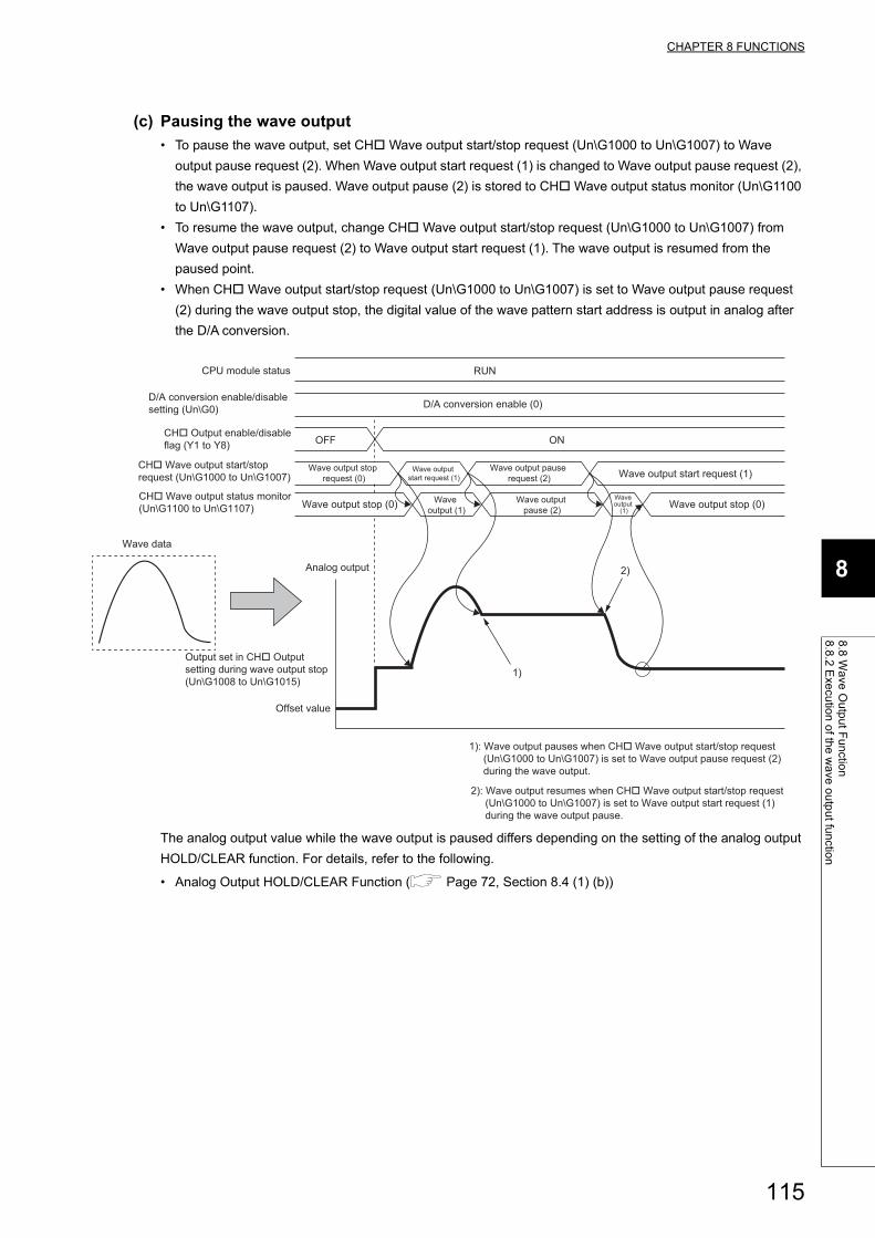
CHAPTER 8 FUNCTIONS
8
8.8
Wa
ve O
utp
ut F
un
ction
8.8
.2 E
xecu
tion
of th
e w
ave
ou
tpu
t fun
ction
(c) Pausing the wave output
• To pause the wave output, set CH Wave output start/stop request (Un\G1000 to Un\G1007) to Wave
output pause request (2). When Wave output start request (1) is changed to Wave output pause request (2),
the wave output is paused. Wave output pause (2) is stored to CH Wave output status monitor (Un\G1100
to Un\G1107).
• To resume the wave output, change CH Wave output start/stop request (Un\G1000 to Un\G1007) from
Wave output pause request (2) to Wave output start request (1). The wave output is resumed from the
paused point.
• When CH Wave output start/stop request (Un\G1000 to Un\G1007) is set to Wave output pause request
(2) during the wave output stop, the digital value of the wave pattern start address is output in analog after
the D/A conversion.
The analog output value while the wave output is paused differs depending on the setting of the analog output
HOLD/CLEAR function. For details, refer to the following.
• Analog Output HOLD/CLEAR Function ( Page 72, Section 8.4 (1) (b))
D/A conversion enable/disable setting (Un\G0)
CPU module status
CH� Output enable/disable flag (Y1 to Y8) OFF ON
D/A conversion enable (0)
Wave output stop request (0)
Wave output pause request (2)
Wave output start request (1) Wave output start request (1)
Wave output stop (0) Wave output pause (2)
Wave output (1)
Wave output
(1)
CH� Wave output start/stop request (Un\G1000 to Un\G1007)
CH� Wave output status monitor (Un\G1100 to Un\G1107)
RUN
Analog output
Offset value
Output set in CH� Outputsetting during wave output stop (Un\G1008 to Un\G1015)
Wave data
1)
Wave output stop (0)
2)
1): Wave output pauses when CH� Wave output start/stop request (Un\G1000 to Un\G1007) is set to Wave output pause request (2) during the wave output.
2): Wave output resumes when CH� Wave output start/stop request (Un\G1000 to Un\G1007) is set to Wave output start request (1) during the wave output pause.
115
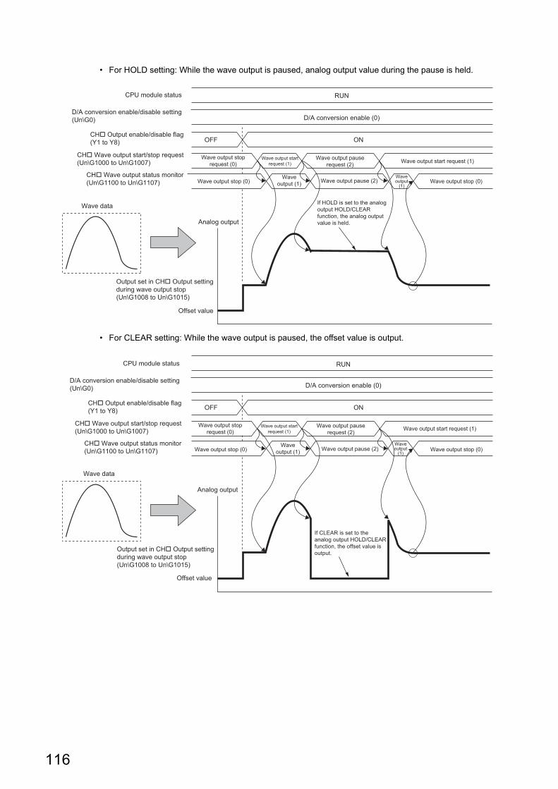
• For HOLD setting: While the wave output is paused, analog output value during the pause is held.
• For CLEAR setting: While the wave output is paused, the offset value is output.
OFF ON
D/A conversion enable (0)
Wave output stoprequest (0)
Wave output pauserequest (2)
Wave output startrequest (1) Wave output start request (1)
Wave output stop (0) Wave output pause (2)Wave
output (1)Waveoutput
(1)
RUN
Analog output
Offset value
Wave data If HOLD is set to the analogoutput HOLD/CLEARfunction, the analog outputvalue is held.
Wave output stop (0)
D/A conversion enable/disable setting(Un\G0)
CPU module status
CH� Output enable/disable flag(Y1 to Y8)
CH� Wave output start/stop request(Un\G1000 to Un\G1007)
CH� Wave output status monitor(Un\G1100 to Un\G1107)
Output set in CH� Output settingduring wave output stop(Un\G1008 to Un\G1015)
OFF ON
Analog output
Wave data
If CLEAR is set to theanalog output HOLD/CLEARfunction, the offset value isoutput.
D/A conversion enable/disable setting(Un\G0)
CPU module status
CH� Output enable/disable flag(Y1 to Y8)
Wave output stoprequest (0)
Wave output pauserequest (2)
Wave output startrequest (1) Wave output start request (1)
Wave output stop (0) Wave output pause (2)Wave
output (1)Waveoutput
(1)
CH� Wave output start/stop request(Un\G1000 to Un\G1007)
CH� Wave output status monitor(Un\G1100 to Un\G1107) Wave output stop (0)
D/A conversion enable (0)
RUN
Offset value
Output set in CH� Output settingduring wave output stop(Un\G1008 to Un\G1015)
116
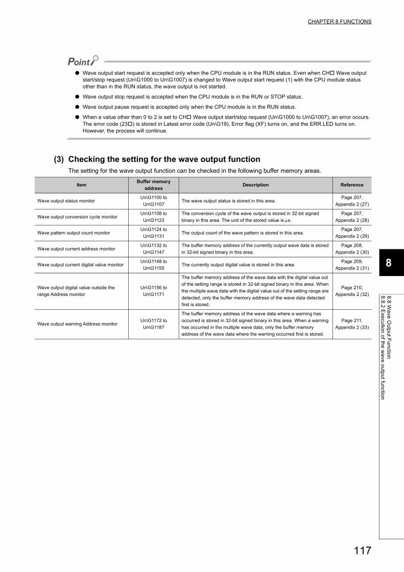
CHAPTER 8 FUNCTIONS
8
8.8
Wa
ve O
utp
ut F
un
ction
8.8
.2 E
xecu
tion
of th
e w
ave
ou
tpu
t fun
ction
● Wave output start request is accepted only when the CPU module is in the RUN status. Even when CH Wave output start/stop request (Un\G1000 to Un\G1007) is changed to Wave output start request (1) with the CPU module status other than in the RUN status, the wave output is not started.
● Wave output stop request is accepted when the CPU module is in the RUN or STOP status.
● Wave output pause request is accepted only when the CPU module is in the RUN status.
● When a value other than 0 to 2 is set to CH Wave output start/stop request (Un\G1000 to Un\G1007), an error occurs. The error code (23) is stored in Latest error code (Un\G19), Error flag (XF) turns on, and the ERR.LED turns on. However, the process will continue.
(3) Checking the setting for the wave output functionThe setting for the wave output function can be checked in the following buffer memory areas.
ItemBuffer memory
addressDescription Reference
Wave output status monitorUn\G1100 to
Un\G1107The wave output status is stored in this area.
Page 207,
Appendix 2 (27)
Wave output conversion cycle monitorUn\G1108 to
Un\G1123
The conversion cycle of the wave output is stored in 32-bit signed
binary in this area. The unit of the stored value is s.
Page 207,
Appendix 2 (28)
Wave pattern output count monitorUn\G1124 to
Un\G1131The output count of the wave pattern is stored in this area.
Page 207,
Appendix 2 (29)
Wave output current address monitorUn\G1132 to
Un\G1147
The buffer memory address of the currently output wave data is stored
in 32-bit signed binary in this area.
Page 208,
Appendix 2 (30)
Wave output current digital value monitorUn\G1148 to
Un\G1155The currently output digital value is stored in this area.
Page 209,
Appendix 2 (31)
Wave output digital value outside the
range Address monitor
Un\G1156 to
Un\G1171
The buffer memory address of the wave data with the digital value out
of the setting range is stored in 32-bit signed binary in this area. When
the multiple wave data with the digital value out of the setting range are
detected, only the buffer memory address of the wave data detected
first is stored.
Page 210,
Appendix 2 (32)
Wave output warning Address monitorUn\G1172 to
Un\G1187
The buffer memory address of the wave data where a warning has
occurred is stored in 32-bit signed binary in this area. When a warning
has occurred in the multiple wave data, only the buffer memory
address of the wave data where the warning occurred first is stored.
Page 211,
Appendix 2 (33)
117
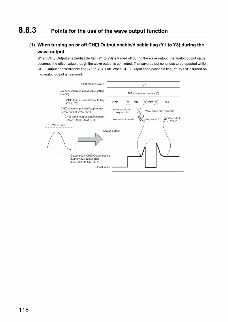
8.8.3 Points for the use of the wave output function
(1) When turning on or off CH Output enable/disable flag (Y1 to Y8) during the
wave outputWhen CH Output enable/disable flag (Y1 to Y8) is turned off during the wave output, the analog output value
becomes the offset value though the wave output is continued. The wave output continues to be updated while
CH Output enable/disable flag (Y1 to Y8) is off. When CH Output enable/disable flag (Y1 to Y8) is turned on,
the analog output is resumed.
OFF ON
D/A conversion enable (0)
Wave output stoprequest (0) Wave output start request (1)
Wave output stop (0) Wave outputstop (0)Wave output (1)
RUN
Analog output
Wave data
OFF ON
D/A conversion enable/disable setting(Un\G0)
CPU module status
CH� Output enable/disable flag(Y1 to Y8)
CH� Wave output start/stop request(Un\G1000 to Un\G1007)
CH� Wave output status monitor(Un\G1100 to Un\G1107)
Offset value
Output set in CH� Output settingduring wave output stop(Un\G1008 to Un\G1015)
118
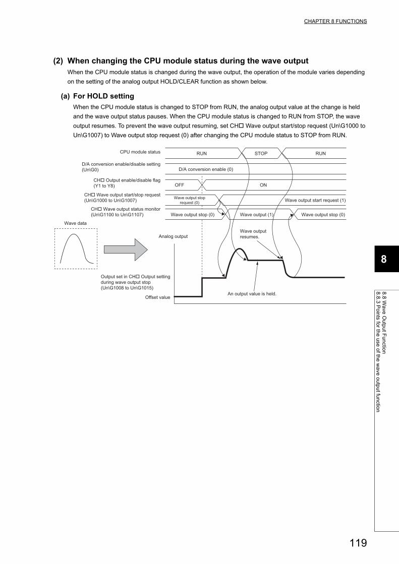
CHAPTER 8 FUNCTIONS
8
8.8
Wa
ve O
utp
ut F
un
ction
8.8
.3 P
oin
ts for th
e u
se o
f the
wa
ve o
utp
ut fu
nctio
n
(2) When changing the CPU module status during the wave outputWhen the CPU module status is changed during the wave output, the operation of the module varies depending
on the setting of the analog output HOLD/CLEAR function as shown below.
(a) For HOLD setting
When the CPU module status is changed to STOP from RUN, the analog output value at the change is held
and the wave output status pauses. When the CPU module status is changed to RUN from STOP, the wave
output resumes. To prevent the wave output resuming, set CH Wave output start/stop request (Un\G1000 to
Un\G1007) to Wave output stop request (0) after changing the CPU module status to STOP from RUN.
OFF ON
D/A conversion enable (0)
Wave output stoprequest (0) Wave output start request (1)
Wave output stop (0) Wave output stop (0)Wave output (1)
STOP RUNRUN
An output value is held.
Wave outputresumes.
D/A conversion enable/disable setting(Un\G0)
CPU module status
CH� Output enable/disable flag(Y1 to Y8)
CH� Wave output start/stop request(Un\G1000 to Un\G1007)
CH� Wave output status monitor(Un\G1100 to Un\G1107)
Offset value
Output set in CH� Output settingduring wave output stop(Un\G1008 to Un\G1015)
Analog output
Wave data
119
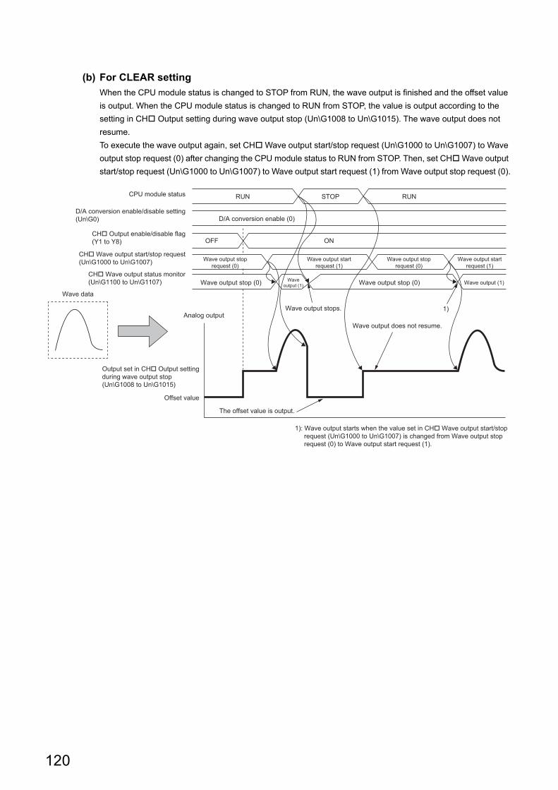
(b) For CLEAR setting
When the CPU module status is changed to STOP from RUN, the wave output is finished and the offset value
is output. When the CPU module status is changed to RUN from STOP, the value is output according to the
setting in CH Output setting during wave output stop (Un\G1008 to Un\G1015). The wave output does not
resume.
To execute the wave output again, set CH Wave output start/stop request (Un\G1000 to Un\G1007) to Wave
output stop request (0) after changing the CPU module status to RUN from STOP. Then, set CH Wave output
start/stop request (Un\G1000 to Un\G1007) to Wave output start request (1) from Wave output stop request (0).
OFF ON
D/A conversion enable (0)
Wave output stoprequest (0)
Wave output stoprequest (0)
Wave output startrequest (1)
Wave output startrequest (1)
Wave output stop (0) Wave output stop (0)Waveoutput (1) Wave output (1)
STOP RUNRUN
The offset value is output.
Wave output does not resume.
Wave output stops.
1): Wave output starts when the value set in CH� Wave output start/stop request (Un\G1000 to Un\G1007) is changed from Wave output stop request (0) to Wave output start request (1).
1)
D/A conversion enable/disable setting(Un\G0)
CPU module status
CH� Output enable/disable flag(Y1 to Y8)
CH� Wave output start/stop request(Un\G1000 to Un\G1007)
CH� Wave output status monitor(Un\G1100 to Un\G1107)
Offset value
Output set in CH� Output settingduring wave output stop(Un\G1008 to Un\G1015)
Wave data
Analog output
120
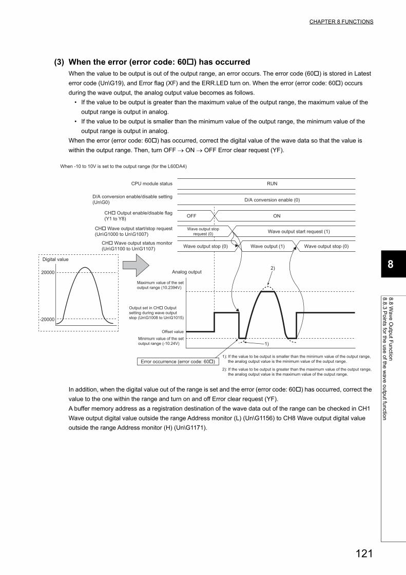
CHAPTER 8 FUNCTIONS
8
8.8
Wa
ve O
utp
ut F
un
ction
8.8
.3 P
oin
ts for th
e u
se o
f the
wa
ve o
utp
ut fu
nctio
n
(3) When the error (error code: 60) has occurredWhen the value to be output is out of the output range, an error occurs. The error code (60) is stored in Latest
error code (Un\G19), and Error flag (XF) and the ERR.LED turn on. When the error (error code: 60) occurs
during the wave output, the analog output value becomes as follows.
• If the value to be output is greater than the maximum value of the output range, the maximum value of the
output range is output in analog.
• If the value to be output is smaller than the minimum value of the output range, the minimum value of the
output range is output in analog.
When the error (error code: 60) has occurred, correct the digital value of the wave data so that the value is
within the output range. Then, turn OFF ON OFF Error clear request (YF).
In addition, when the digital value out of the range is set and the error (error code: 60) has occurred, correct the
value to the one within the range and turn on and off Error clear request (YF).
A buffer memory address as a registration destination of the wave data out of the range can be checked in CH1
Wave output digital value outside the range Address monitor (L) (Un\G1156) to CH8 Wave output digital value
outside the range Address monitor (H) (Un\G1171).
OFF ON
D/A conversion enable (0)
Wave output stoprequest (0) Wave output start request (1)
Wave output stop (0) Wave output stop (0)Wave output (1)
RUN
Analog output
Offset value
Minimum value of the setoutput range (-10.24V)
Maximum value of the setoutput range (10.2394V)
Output set in CH� Outputsetting during wave outputstop (Un\G1008 to Un\G1015)
Digital value
-20000
20000
Error occurrence (error code: 60�)
1)
1): If the value to be output is smaller than the minimum value of the output range, the analog output value is the minimum value of the output range.
2): If the value to be output is greater than the maximum value of the output range, the analog output value is the maximum value of the output range.
2)
When -10 to 10V is set to the output range (for the L60DA4)
D/A conversion enable/disable setting(Un\G0)
CPU module status
CH� Output enable/disable flag(Y1 to Y8)
CH� Wave output start/stop request(Un\G1000 to Un\G1007)
CH� Wave output status monitor(Un\G1100 to Un\G1107)
121
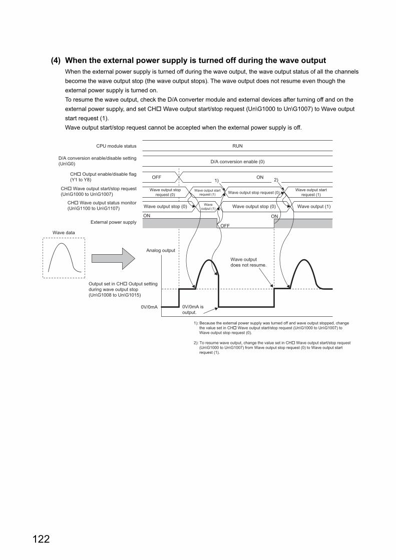
(4) When the external power supply is turned off during the wave outputWhen the external power supply is turned off during the wave output, the wave output status of all the channels
become the wave output stop (the wave output stops). The wave output does not resume even though the
external power supply is turned on.
To resume the wave output, check the D/A converter module and external devices after turning off and on the
external power supply, and set CH Wave output start/stop request (Un\G1000 to Un\G1007) to Wave output
start request (1).
Wave output start/stop request cannot be accepted when the external power supply is off.
OFF ON
D/A conversion enable (0)
Wave output stoprequest (0) Wave output stop request (0)Wave output start
request (1)Wave output start
request (1)
Wave output stop (0) Wave output stop (0)Waveoutput (1) Wave output (1)
External power supply
RUN
Analog output
0V/0mA
Output set in CH� Output settingduring wave output stop(Un\G1008 to Un\G1015)
Wave dataOFF
ONON
Wave outputdoes not resume.
0V/0mA isoutput.
2): To resume wave output, change the value set in CH� Wave output start/stop request (Un\G1000 to Un\G1007) from Wave output stop request (0) to Wave output start request (1).
1): Because the external power supply was turned off and wave output stopped, change the value set in CH� Wave output start/stop request (Un\G1000 to Un\G1007) to Wave output stop request (0).
1) 2)
D/A conversion enable/disable setting(Un\G0)
CPU module status
CH� Output enable/disable flag(Y1 to Y8)
CH� Wave output start/stop request(Un\G1000 to Un\G1007)
CH� Wave output status monitor(Un\G1100 to Un\G1107)
122
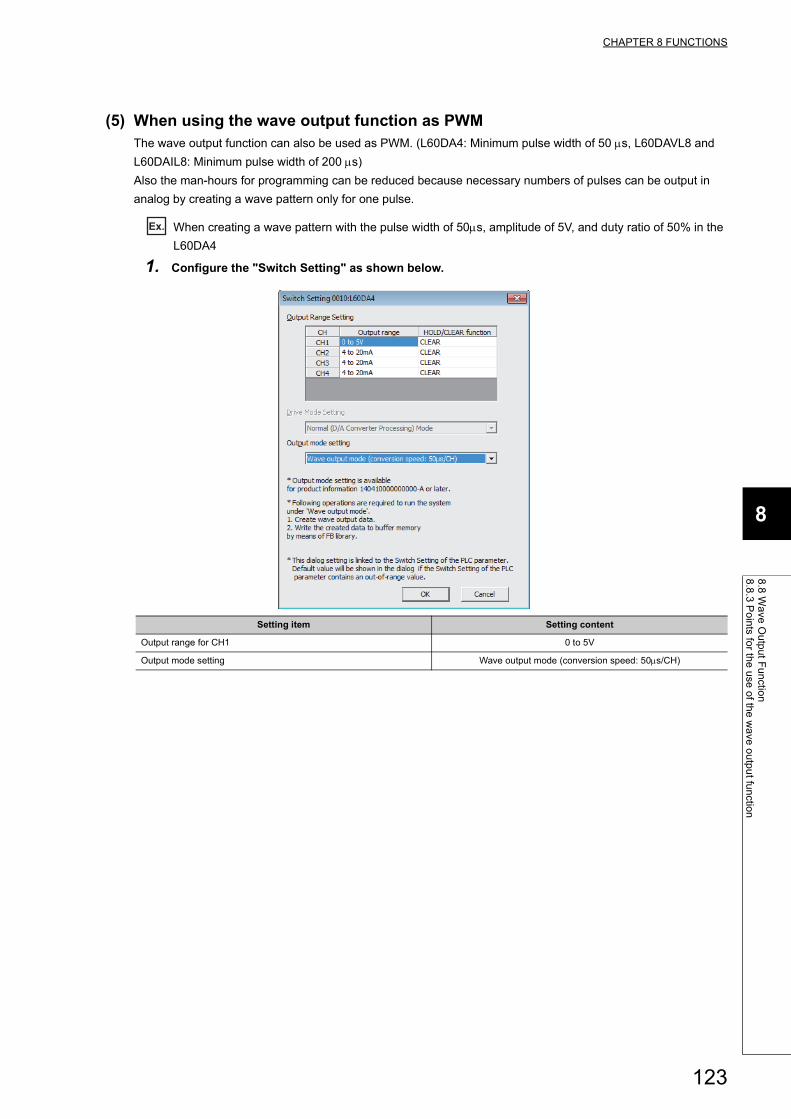
CHAPTER 8 FUNCTIONS
8
8.8
Wa
ve O
utp
ut F
un
ction
8.8
.3 P
oin
ts for th
e u
se o
f the
wa
ve o
utp
ut fu
nctio
n
(5) When using the wave output function as PWMThe wave output function can also be used as PWM. (L60DA4: Minimum pulse width of 50 s, L60DAVL8 and
L60DAIL8: Minimum pulse width of 200 s)
Also the man-hours for programming can be reduced because necessary numbers of pulses can be output in
analog by creating a wave pattern only for one pulse.
Ex. When creating a wave pattern with the pulse width of 50s, amplitude of 5V, and duty ratio of 50% in the
L60DA4
1. Configure the "Switch Setting" as shown below.
Setting item Setting content
Output range for CH1 0 to 5V
Output mode setting Wave output mode (conversion speed: 50s/CH)
123
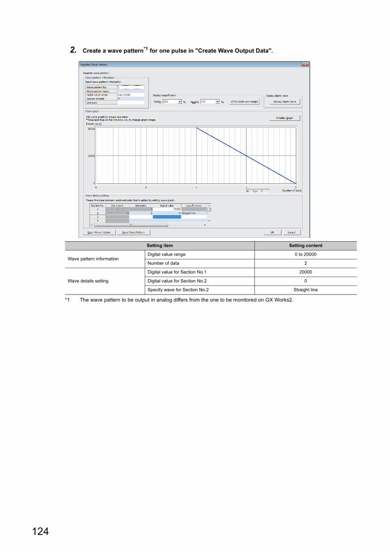
2. Create a wave pattern*1 for one pulse in "Create Wave Output Data".
*1 The wave pattern to be output in analog differs from the one to be monitored on GX Works2.
Setting item Setting content
Wave pattern informationDigital value range 0 to 20000
Number of data 2
Wave details setting
Digital value for Section No.1 20000
Digital value for Section No.2 0
Specify wave for Section No.2 Straight line
124
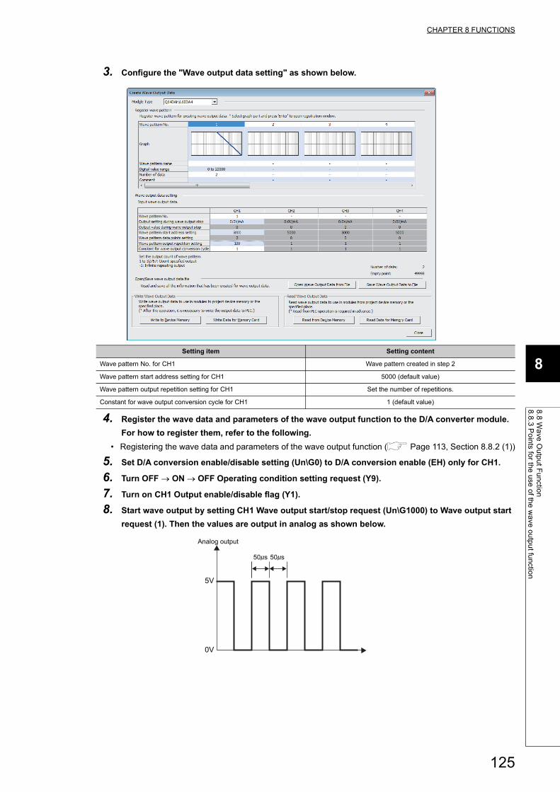
CHAPTER 8 FUNCTIONS
8
8.8
Wa
ve O
utp
ut F
un
ction
8.8
.3 P
oin
ts for th
e u
se o
f the
wa
ve o
utp
ut fu
nctio
n
3. Configure the "Wave output data setting" as shown below.
4. Register the wave data and parameters of the wave output function to the D/A converter module.
For how to register them, refer to the following.
• Registering the wave data and parameters of the wave output function ( Page 113, Section 8.8.2 (1))
5. Set D/A conversion enable/disable setting (Un\G0) to D/A conversion enable (EH) only for CH1.
6. Turn OFF ON OFF Operating condition setting request (Y9).
7. Turn on CH1 Output enable/disable flag (Y1).
8. Start wave output by setting CH1 Wave output start/stop request (Un\G1000) to Wave output start
request (1). Then the values are output in analog as shown below.
Setting item Setting content
Wave pattern No. for CH1 Wave pattern created in step 2
Wave pattern start address setting for CH1 5000 (default value)
Wave pattern output repetition setting for CH1 Set the number of repetitions.
Constant for wave output conversion cycle for CH1 1 (default value)
50 s 50 s
0V
5V
Analog output
125
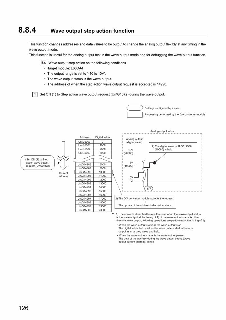
8.8.4 Wave output step action function
This function changes addresses and data values to be output to change the analog output flexibly at any timing in the
wave output mode.
This function is useful for the analog output test in the wave output mode and for debugging the wave output function.
Ex. Wave output step action on the following conditions
• Target module: L60DA4
• The output range is set to "-10 to 10V".
• The wave output status is the wave output.
• The address of when the step action wave output request is accepted is 14990.
Currentaddress 0V
(0)
10V(20000)
5V(10000)
Digital value
2) The D/A converter module accepts the request.
The update of the address to be output stops.↓
2) The digital value of Un\G14990 (10000) is held.
1)*1
1) Set ON (1) to Step action wave output request (Un\G1072).*1
Analog output value
: Settings configured by a user
Address
*1 1) The contents described here is the case when the wave output status is the wave output at the timing of 1). If the wave output status is other than the wave output, following operations are performed at the timing of 2).
� When the wave output status is the wave output stop The digital value that is set as the wave pattern start address is output in an analog value and held.� When the wave output status is the wave output pause The data of the address during the wave output pause (wave output current address) is held.
1 Set ON (1) to Step action wave output request (Un\G1072) during the wave output.
Un\G5000Un\G5001Un\G5002Un\G5003
Un\G14988Un\G14989Un\G14990Un\G14991Un\G14992Un\G14993Un\G14994Un\G14995Un\G14996Un\G14997Un\G14998
0100020003000
80009000100001100012000130001400015000160001700018000
Un\G14999 19000Un\G15000 20000
: Processing performed by the D/A converter module
Analog output(digital value)
126
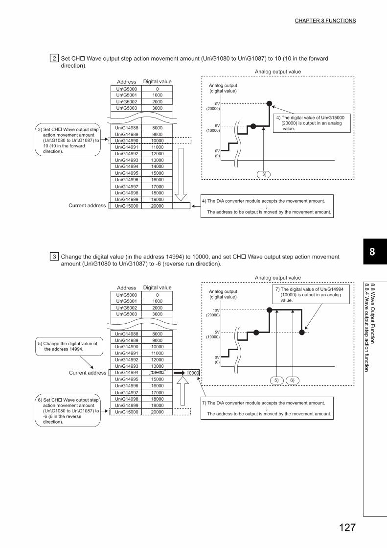
CHAPTER 8 FUNCTIONS
8
8.8
Wa
ve O
utp
ut F
un
ction
8.8
.4 W
ave
ou
tpu
t step
actio
n fu
nctio
n
Un\G5000Un\G5001Un\G5002Un\G5003
Un\G14988Un\G14989Un\G14990
Current address
Un\G14991Un\G14992Un\G14993Un\G14994Un\G14995Un\G14996Un\G14997Un\G14998Un\G14999Un\G15000
0100020003000
80009000
1000011000120001300014000150001600017000180001900020000
Digital value
4) The D/A converter module accepts the movement amount.
The address to be output is moved by the movement amount.
3) Set CH� Wave output step action movement amount (Un\G1080 to Un\G1087) to 10 (10 in the forward direction).
Address
2 Set CH� Wave output step action movement amount (Un\G1080 to Un\G1087) to 10 (10 in the forward direction).
Analog output(digital value)
4) The digital value of Un/G15000 (20000) is output in an analog value.
3)
Analog output value
Un\G5000Un\G5001Un\G5002Un\G5003
Un\G14988Un\G14989Un\G14990
Current address
Un\G14991Un\G14992Un\G14993Un\G14994Un\G14995Un\G14996Un\G14997Un\G14998Un\G14999Un\G15000
0100020003000
80009000
1000011000120001300014000 10000150001600017000180001900020000
Digital value
5) Change the digital value of the address 14994.
AddressAnalog output(digital value)
7) The digital value of Un/G14994 (10000) is output in an analog value.
5)
Analog output value
6)
6) Set CH� Wave output step action movement amount (Un\G1080 to Un\G1087) to -6 (6 in the reverse direction).
3 Change the digital value (in the address 14994) to 10000, and set CH� Wave output step action movement amount (Un\G1080 to Un\G1087) to -6 (reverse run direction).
↓
7) The D/A converter module accepts the movement amount.
The address to be output is moved by the movement amount.↓
0V(0)
10V(20000)
5V(10000)
0V(0)
10V(20000)
5V(10000)
127
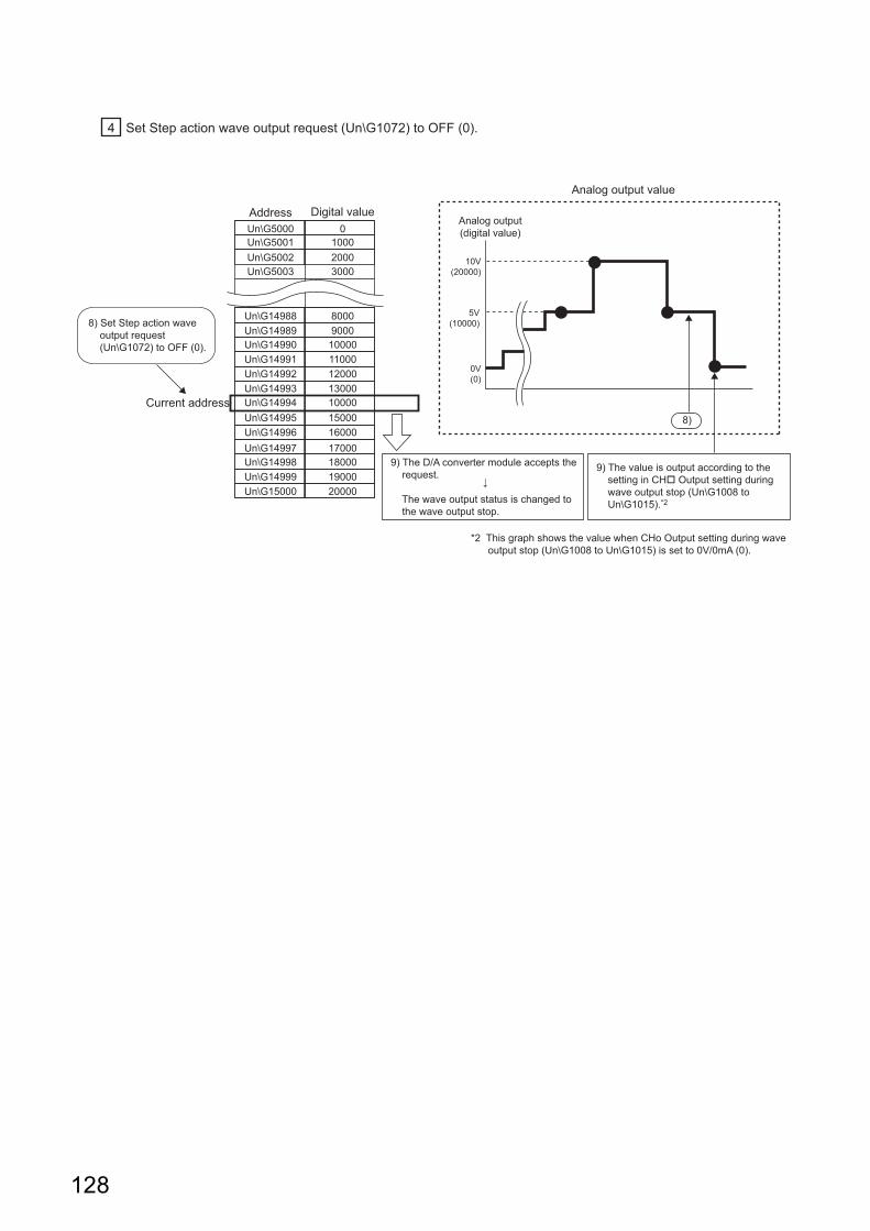
Un\G5000Un\G5001Un\G5002Un\G5003
Un\G14988Un\G14989Un\G14990
Current address
Un\G14991Un\G14992Un\G14993Un\G14994Un\G14995Un\G14996Un\G14997Un\G14998Un\G14999Un\G15000
0100020003000
80009000
1000011000120001300010000150001600017000180001900020000
Digital value
9) The D/A converter module accepts the request.
The wave output status is changed to the wave output stop.
Address
4 Set Step action wave output request (Un\G1072) to OFF (0).
Analog output(digital value)
Analog output value
8)
8) Set Step action wave output request (Un\G1072) to OFF (0).
9) The value is output according to the setting in CH� Output setting during wave output stop (Un\G1008 to Un\G1015).*2
*2 This graph shows the value when CHo Output setting during wave output stop (Un\G1008 to Un\G1015) is set to 0V/0mA (0).
↓
0V(0)
10V(20000)
5V(10000)
128
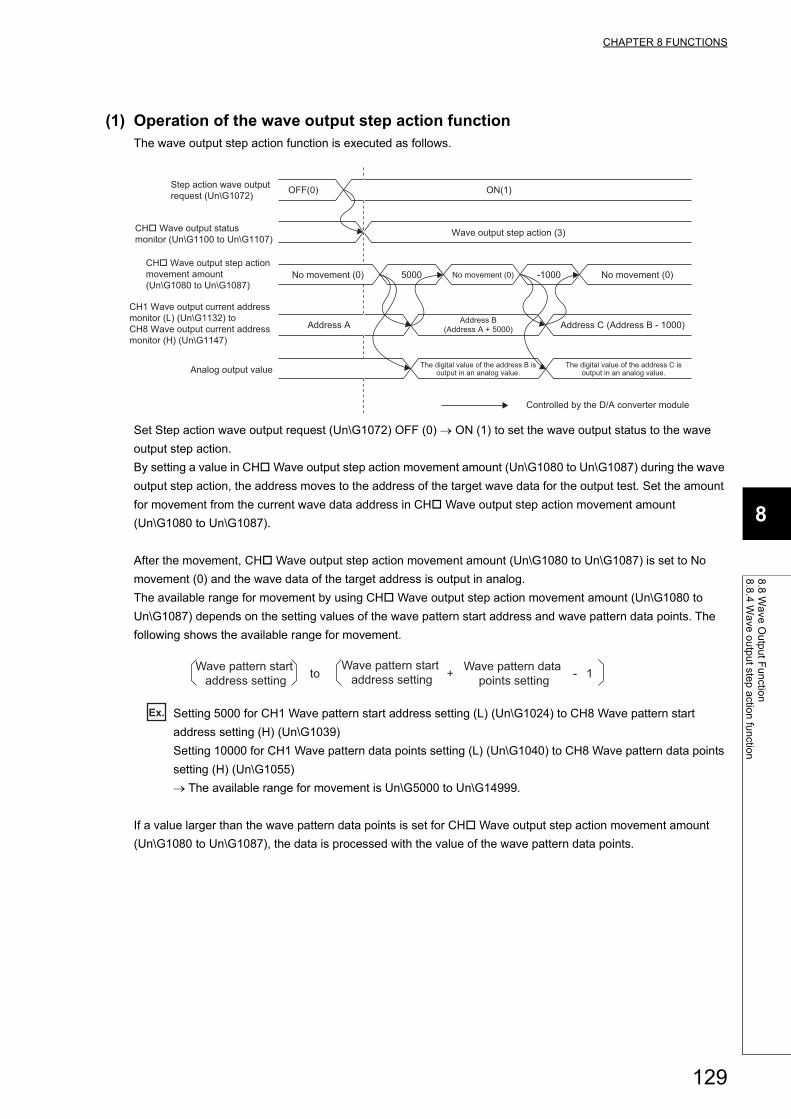
CHAPTER 8 FUNCTIONS
8
8.8
Wa
ve O
utp
ut F
un
ction
8.8
.4 W
ave
ou
tpu
t step
actio
n fu
nctio
n
(1) Operation of the wave output step action functionThe wave output step action function is executed as follows.
Set Step action wave output request (Un\G1072) OFF (0) ON (1) to set the wave output status to the wave
output step action.
By setting a value in CH Wave output step action movement amount (Un\G1080 to Un\G1087) during the wave
output step action, the address moves to the address of the target wave data for the output test. Set the amount
for movement from the current wave data address in CH Wave output step action movement amount
(Un\G1080 to Un\G1087).
After the movement, CH Wave output step action movement amount (Un\G1080 to Un\G1087) is set to No
movement (0) and the wave data of the target address is output in analog.
The available range for movement by using CH Wave output step action movement amount (Un\G1080 to
Un\G1087) depends on the setting values of the wave pattern start address and wave pattern data points. The
following shows the available range for movement.
Ex. Setting 5000 for CH1 Wave pattern start address setting (L) (Un\G1024) to CH8 Wave pattern start
address setting (H) (Un\G1039)
Setting 10000 for CH1 Wave pattern data points setting (L) (Un\G1040) to CH8 Wave pattern data points
setting (H) (Un\G1055)
The available range for movement is Un\G5000 to Un\G14999.
If a value larger than the wave pattern data points is set for CH Wave output step action movement amount
(Un\G1080 to Un\G1087), the data is processed with the value of the wave pattern data points.
OFF(0) ON(1)
Wave output step action (3)
Address A Address B(Address A + 5000) Address C (Address B - 1000)
No movement (0) No movement (0)5000 -1000No movement (0)
The digital value of the address B isoutput in an analog value.
The digital value of the address C isoutput in an analog value.
Step action wave output request (Un\G1072)
Analog output value
CH� Wave output status monitor (Un\G1100 to Un\G1107)
CH� Wave output step action movement amount (Un\G1080 to Un\G1087)
CH1 Wave output current address monitor (L) (Un\G1132) to CH8 Wave output current address monitor (H) (Un\G1147)
Controlled by the D/A converter module
Wave pattern start address setting to + Wave pattern data
points setting - 1Wave pattern start
address setting
129
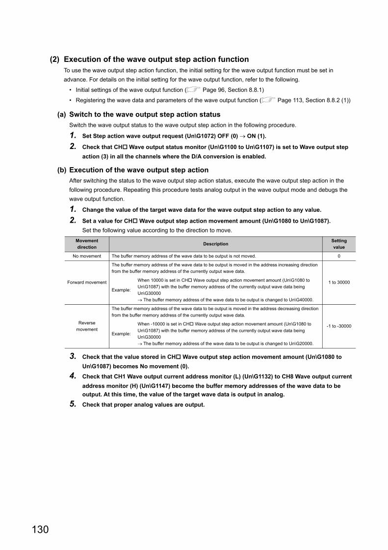
(2) Execution of the wave output step action functionTo use the wave output step action function, the initial setting for the wave output function must be set in
advance. For details on the initial setting for the wave output function, refer to the following.
• Initial settings of the wave output function ( Page 96, Section 8.8.1)
• Registering the wave data and parameters of the wave output function ( Page 113, Section 8.8.2 (1))
(a) Switch to the wave output step action status
Switch the wave output status to the wave output step action in the following procedure.
1. Set Step action wave output request (Un\G1072) OFF (0) ON (1).
2. Check that CH Wave output status monitor (Un\G1100 to Un\G1107) is set to Wave output step
action (3) in all the channels where the D/A conversion is enabled.
(b) Execution of the wave output step action
After switching the status to the wave output step action status, execute the wave output step action in the
following procedure. Repeating this procedure tests analog output in the wave output mode and debugs the
wave output function.
1. Change the value of the target wave data for the wave output step action to any value.
2. Set a value for CH Wave output step action movement amount (Un\G1080 to Un\G1087).
Set the following value according to the direction to move.
3. Check that the value stored in CH Wave output step action movement amount (Un\G1080 to
Un\G1087) becomes No movement (0).
4. Check that CH1 Wave output current address monitor (L) (Un\G1132) to CH8 Wave output current
address monitor (H) (Un\G1147) become the buffer memory addresses of the wave data to be
output. At this time, the value of the target wave data is output in analog.
5. Check that proper analog values are output.
Movement
directionDescription
Setting
value
No movement The buffer memory address of the wave data to be output is not moved. 0
Forward movement
The buffer memory address of the wave data to be output is moved in the address increasing direction
from the buffer memory address of the currently output wave data.
1 to 30000
Example:
When 10000 is set in CH Wave output step action movement amount (Un\G1080 to
Un\G1087) with the buffer memory address of the currently output wave data being
Un\G30000
The buffer memory address of the wave data to be output is changed to Un\G40000.
Reverse
movement
The buffer memory address of the wave data to be output is moved in the address decreasing direction
from the buffer memory address of the currently output wave data.
-1 to -30000
Example:
When -10000 is set in CH Wave output step action movement amount (Un\G1080 to
Un\G1087) with the buffer memory address of the currently output wave data being
Un\G30000
The buffer memory address of the wave data to be output is changed to Un\G20000.
130
CHAPTER 8 FUNCTIONS
8
8.8
Wa
ve O
utp
ut F
un
ction
8.8
.4 W
ave
ou
tpu
t step
actio
n fu
nctio
n
(c) End of the wave output step action
End the wave output step action in the following procedure.
1. Set Step action wave output request (Un\G1072) ON(1) OFF(0).
2. Check that CH Wave output status monitor (Un\G1100 to Un\G1107) becomes Wave output stop
(0) in all the channels. If CH Wave output start/stop request (Un\G1000 to Un\G1007) is set to a
value other than Wave output stop request (0), the value is changed to Wave output stop request
(0) forcibly at this timing. Check also the value of this buffer memory area.
To execute the wave output after the wave output step action, set CH Wave output start/stop request
(Un\G1000 to Un\G1007) to Wave output start request (1).
● Analog output may be changed significantly when a value is set for CH Wave output step action movement amount (Un\G1080 to Un\G1087). To prevent a significant change, use CH Output enable/disable flag (Y1 to Y8) if necessary. For details, refer to the following.
• Analog Output HOLD/CLEAR Function ( Page 71, Section 8.4)In addition, during the wave output step action, analog output can be changed at any timing by using CH Output enable/disable flag (Y1 to Y8). For details, refer to the following.
• Analog output test in the wave output mode ( Page 132, Section 8.8.4 (3))
● During the wave output step action, the wave output status is not changed even if a value is set for CH Wave output start/stop request (Un\G1000 to Un\G1007). To change the wave output status, set Step action wave output request (Un\G1072) to OFF (0) (set the status to the wave output stop).
131
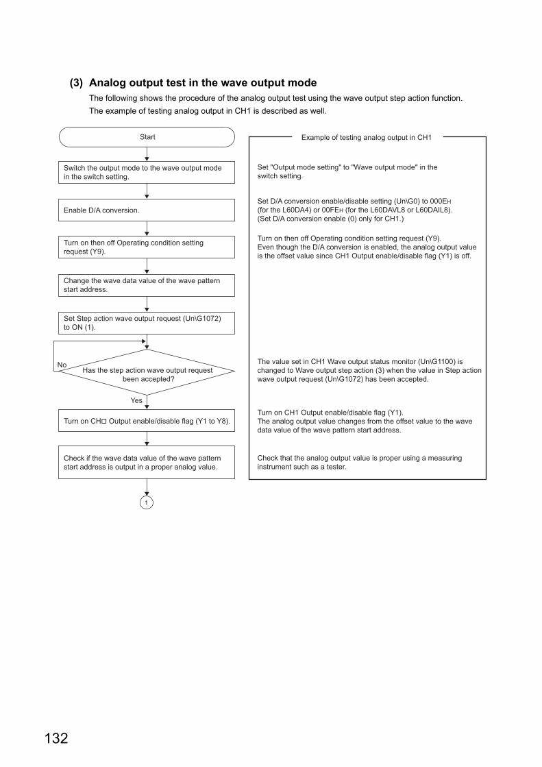
(3) Analog output test in the wave output modeThe following shows the procedure of the analog output test using the wave output step action function.
The example of testing analog output in CH1 is described as well.
1
Switch the output mode to the wave output mode in the switch setting.
Set "Output mode setting" to "Wave output mode" in the switch setting.
Set D/A conversion enable/disable setting (Un\G0) to 000EH (for the L60DA4) or 00FEH (for the L60DAVL8 or L60DAIL8).(Set D/A conversion enable (0) only for CH1.)
Enable D/A conversion.
Change the wave data value of the wave pattern start address.
Turn on then off Operating condition setting request (Y9).
Set Step action wave output request (Un\G1072) to ON (1).
The value set in CH1 Wave output status monitor (Un\G1100) ischanged to Wave output step action (3) when the value in Step actionwave output request (Un\G1072) has been accepted.
Check if the wave data value of the wave pattern start address is output in a proper analog value.
Turn on CH� Output enable/disable flag (Y1 to Y8).Turn on CH1 Output enable/disable flag (Y1). The analog output value changes from the offset value to the wave data value of the wave pattern start address.
Check that the analog output value is proper using a measuringinstrument such as a tester.
Start Example of testing analog output in CH1
Turn on then off Operating condition setting request (Y9).Even though the D/A conversion is enabled, the analog output value is the offset value since CH1 Output enable/disable flag (Y1) is off.
Has the step action wave output request been accepted?
Yes
No
132
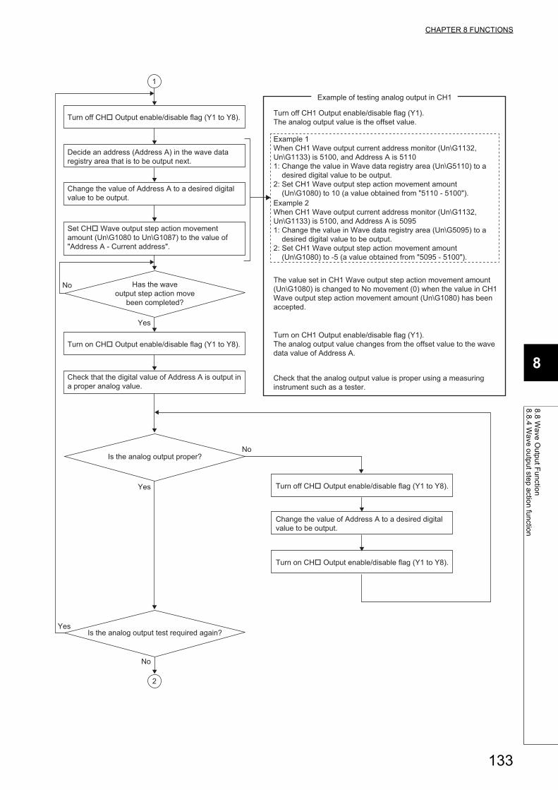
CHAPTER 8 FUNCTIONS
8
8.8
Wa
ve O
utp
ut F
un
ction
8.8
.4 W
ave
ou
tpu
t step
actio
n fu
nctio
n
1
2
Turn off CH� Output enable/disable flag (Y1 to Y8).
Decide an address (Address A) in the wave dataregistry area that is to be output next.
Change the value of Address A to a desired digitalvalue to be output.
Set CH� Wave output step action movementamount (Un\G1080 to Un\G1087) to the value of"Address A - Current address".
Turn off CH� Output enable/disable flag (Y1 to Y8).
Change the value of Address A to a desired digitalvalue to be output.
Turn on CH� Output enable/disable flag (Y1 to Y8).
The value set in CH1 Wave output step action movement amount(Un\G1080) is changed to No movement (0) when the value in CH1Wave output step action movement amount (Un\G1080) has beenaccepted.
Example 1When CH1 Wave output current address monitor (Un\G1132,Un\G1133) is 5100, and Address A is 51101: Change the value in Wave data registry area (Un\G5110) to a desired digital value to be output. 2: Set CH1 Wave output step action movement amount (Un\G1080) to 10 (a value obtained from "5110 - 5100").Example 2When CH1 Wave output current address monitor (Un\G1132,Un\G1133) is 5100, and Address A is 50951: Change the value in Wave data registry area (Un\G5095) to a desired digital value to be output. 2: Set CH1 Wave output step action movement amount (Un\G1080) to -5 (a value obtained from "5095 - 5100").
Turn off CH1 Output enable/disable flag (Y1).The analog output value is the offset value.
Turn on CH1 Output enable/disable flag (Y1).The analog output value changes from the offset value to the wave data value of Address A.
Check that the analog output value is proper using a measuring instrument such as a tester.
Example of testing analog output in CH1
Turn on CH� Output enable/disable flag (Y1 to Y8).
Check that the digital value of Address A is output ina proper analog value.
Is the analog output proper?
Has the waveoutput step action move
been completed?
Yes
Yes
No
No
Is the analog output test required again?
No
Yes
133
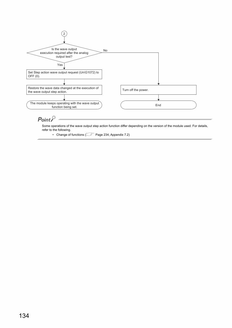
Some operations of the wave output step action function differ depending on the version of the module used. For details, refer to the following.
• Change of functions ( Page 234, Appendix 7.2)
2
Set Step action wave output request (Un\G1072) toOFF (0).
The module keeps operating with the wave outputfunction being set. End
Turn off the power.
Is the wave outputexecution required after the analog
output test?
No
Yes
Restore the wave data changed at the execution of the wave output step action.
134
CHAPTER 8 FUNCTIONS
8
8.9
Erro
r Lo
g F
un
ction
8.9 Error Log Function
This function stores a history of errors and alarms that occurred in the D/A converter module to the buffer memory
(Un\G1810 to Un\G1969).
A total of 16 errors and alarms can be stored.
(1) Process of the error log functionThe error code and the error time are stored in the buffer memory area, starting from Error history No.1 (start
address: Un\G1810) and sequentially thereafter. Error time is stored as follows.
Ex. For error history No. 1
*1 Those are values when an error occurs at 10:35:40 on Tuesday, March 29th, 2011.
(2) Clearing error historyError history can be cleared by any of the following methods.
• Turning off the power supply
• Resetting the CPU module
• Setting Error history clear setting (Un\G1802) to Clear (1), and then turning on and off Error clear request
(YF) or Operating condition setting request (Y9). (L60DAVL8 and L60DAIL8 only)
Item Stored data Example*1
First two digits of the year/Last
two digits of the year
Stored in BCD code.
2011H
Month/Day 0329H
Hour/Minute 1035H
Second 40H
Day of the week
The value that corresponds to the day of the week is stored in BCD code.
• Sunday: 0
• Monday: 1
• Tuesday: 2
• Wednesday: 3
• Thursday: 4
• Friday: 5
• Saturday: 6
02H
Common
b15 to b8 b7 b0to
Error code
First two digits of the year Last two digits of the year
Month Day
Hour Minute
Second Day of the week
Un\G1810
Un\G1814
Un\G1813
Un\G1812
Un\G1811
Un\G1815
Un\G1819
System areato
135
(3) Checking error historyThe start address of the latest stored error can be checked in Latest address of error history (Un\G1800).
Ex. When the third error occurs:
The third error is stored in error history No.3, and the value "1830" (start address of error history No.3) is
stored to Latest address of error history (Un\G1800).
The start address of the error historywhere the latest error is stored is stored.
Error history No.1
Error history No.2
Error history No.3
Error history No.16
(Empty)
(Empty)
New
Address1810
1820
1830
1960
1st error
2nd error
3rd error
An error history consists of the followingdata.
Details of error history
Error code
Erroroccurrencetime
First two digits of the year Last two digits of the year
MonthHour
Second
DayMinute
Day of the week
Latest address of errorhistory (Un\G1800)
136
CHAPTER 8 FUNCTIONS
8
8.9
Erro
r Lo
g F
un
ction
Ex. When the 17th error occurs:
The 17th error is stored in error history No.1, and the value "1810" (start address of error history No.1) is
stored to Latest address of error history (Un\G1800).
● The same process for errors is used when an alarm occurs.
● Once the error history storage area becomes full, subsequent error information will overwrite the existing data, starting from Error history No.1 (Un\G1810 to Un\G1819), and continues sequentially thereafter. (The overwritten history is deleted.)
Error history No.1
Error history No.2
Error history No.3
Error history No.16
New
The 17th error is stored in Error history No.1 and the 1st error history will be erased.
Address1810
1820
1830
1960
1st error
2nd error
3rd error
16th error
17th error
Latest address of error history(Un\G1800)
137
8.10 Module Error Collection Function
This function collects the errors and alarms caused in the D/A converter module into the CPU module. By holding the
module errors in a CPU module memory that can hold data in the event of power failure, the details on errors can be
held even after the module is powered off or reset.
For details on the module error collection function, refer to the following.
MELSEC-L CPU Module User's Manual (Function Explanation, Program Fundamentals)
Common
Error history (CPU module including built-in I/O and built-inCC-Link) and error log (intelligent function module) aredisplayed on one screen.
Errors that occurred in the entire system can be monitored in reverse chronological order.
Programming tool
[Example of screen display]
Error history display
19:29
19:33
19:34
19:36
Module A
CPU
Module B
Module A
Error A1
Error C1
Error B1
Error A2
Time Module in error Error code
Error history (CPU module) Module error log
Time Module in error Error code
19:29
19:34
19:36
Module A
Module B
Module A
Error A1
Error B1
Error A2
19:33 Error C1
CPU
Module A Module B
19:33 Error C1 occurred!
19:29 Error A1 occurred! 19:36 Error A2 occurred!
19:34 Error B1 occurred!
138
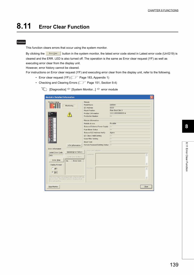
CHAPTER 8 FUNCTIONS
8
8.1
1 E
rror C
lea
r Fu
nctio
n
8.11 Error Clear Function
This function clears errors that occur using the system monitor.
By clicking the button in the system monitor, the latest error code stored in Latest error code (Un\G19) is
cleared and the ERR. LED is also turned off. The operation is the same as Error clear request (YF) as well as
executing error clear from the display unit.
However, error history cannot be cleared.
For instructions on Error clear request (YF) and executing error clear from the display unit, refer to the following.
• Error clear request (YF) ( Page 183, Appendix 1)
• Checking and Clearing Errors ( Page 151, Section 9.4)
[Diagnostics] [System Monitor...] error module
Common
139
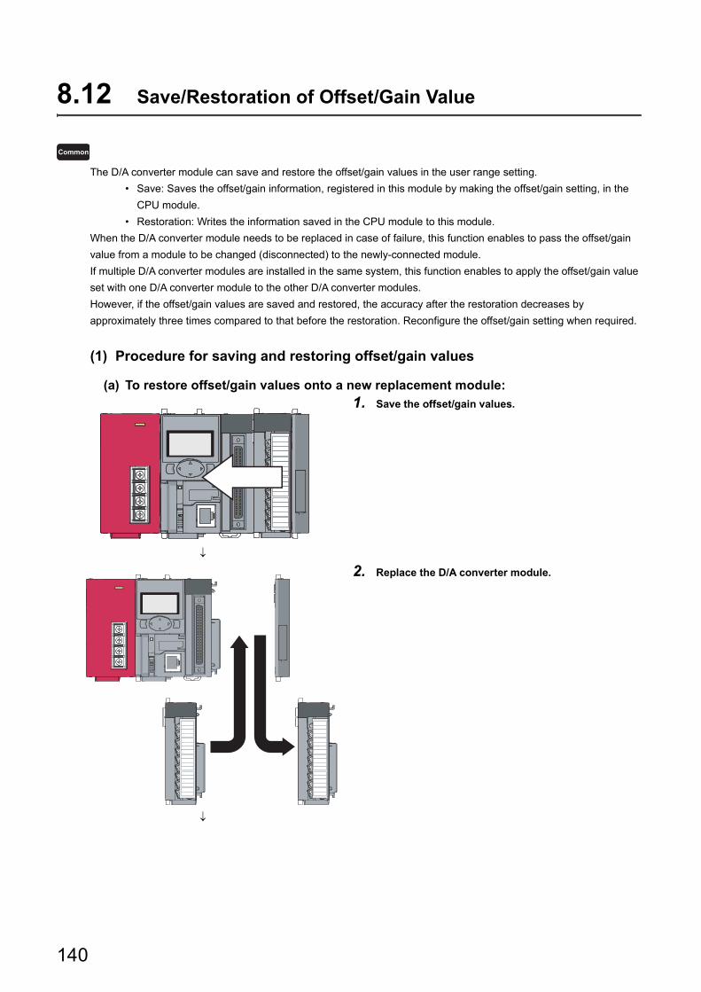
8.12 Save/Restoration of Offset/Gain Value
The D/A converter module can save and restore the offset/gain values in the user range setting.
• Save: Saves the offset/gain information, registered in this module by making the offset/gain setting, in the
CPU module.
• Restoration: Writes the information saved in the CPU module to this module.
When the D/A converter module needs to be replaced in case of failure, this function enables to pass the offset/gain
value from a module to be changed (disconnected) to the newly-connected module.
If multiple D/A converter modules are installed in the same system, this function enables to apply the offset/gain value
set with one D/A converter module to the other D/A converter modules.
However, if the offset/gain values are saved and restored, the accuracy after the restoration decreases by
approximately three times compared to that before the restoration. Reconfigure the offset/gain setting when required.
(1) Procedure for saving and restoring offset/gain values
(a) To restore offset/gain values onto a new replacement module:
1. Save the offset/gain values.
2. Replace the D/A converter module.
Common
140
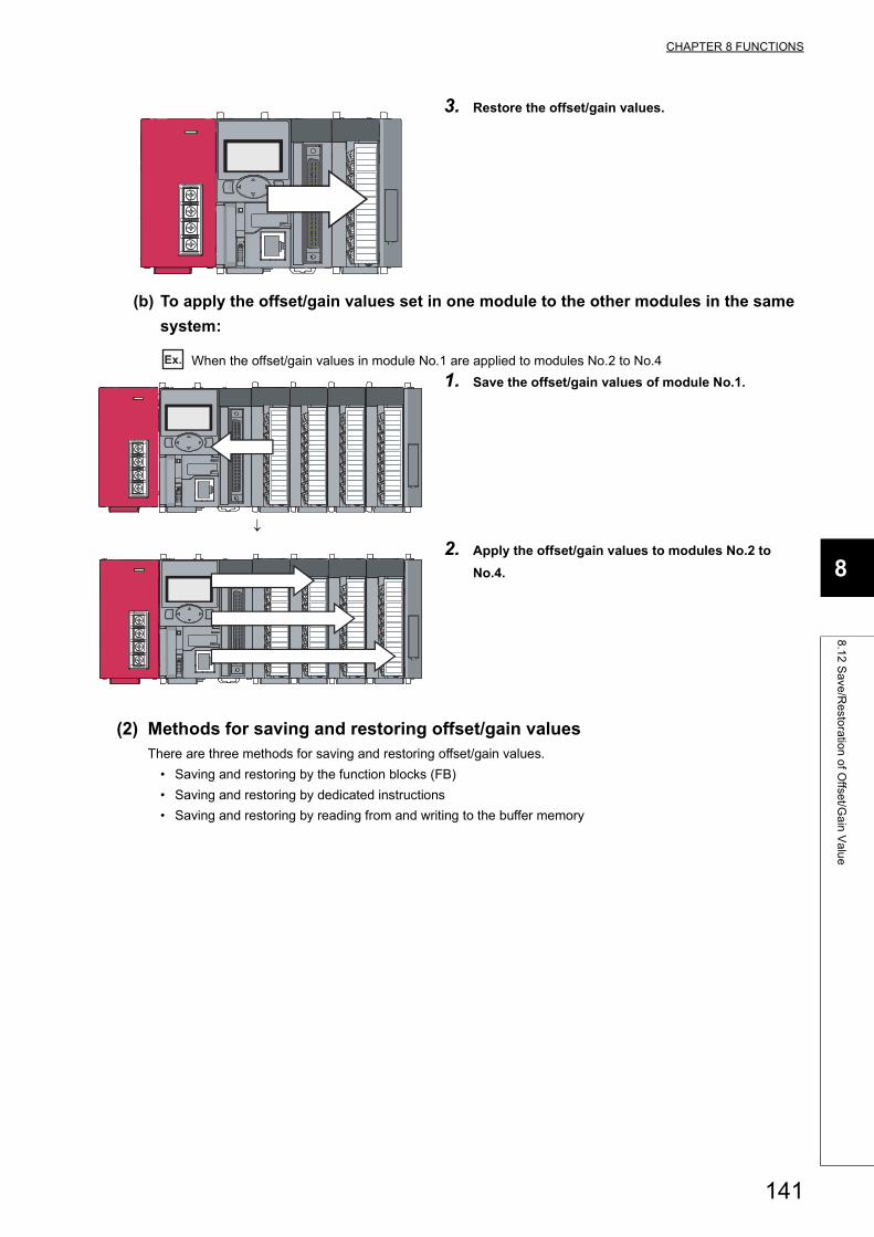
CHAPTER 8 FUNCTIONS
8
8.1
2 S
ave
/Re
stora
tion
of O
ffset/G
ain
Va
lue
(b) To apply the offset/gain values set in one module to the other modules in the same
system:
Ex. When the offset/gain values in module No.1 are applied to modules No.2 to No.4
(2) Methods for saving and restoring offset/gain valuesThere are three methods for saving and restoring offset/gain values.
• Saving and restoring by the function blocks (FB)
• Saving and restoring by dedicated instructions
• Saving and restoring by reading from and writing to the buffer memory
3. Restore the offset/gain values.
1. Save the offset/gain values of module No.1.
2. Apply the offset/gain values to modules No.2 to
No.4.
141
(a) Saving and restoring by the function blocks (FB)
Temporarily save the offset/gain values in the source D/A converter module into an SD memory card inserted in
the CPU module by using the function block (FB) to save the offset/gain values. After that, write the values to
the destination D/A converter module by using the function block (FB) to restore the offset/gain values.
Since the offset/gain values are saved in the SD memory card, the saved data are not erased even if the
system is powered off for replacement of a module.
For details on the function blocks (FB), refer to the following.
MELSEC-L Digital-Analog Converter Module FB Library Reference Manual
(FBM-M031)
MELSEC-L Digital-Analog Converter Module FB Library (CC-Link IE Field compatible) Reference
Manual (FBM-M072)
MELSEC-L Digital-Analog Converter Module FB Library Reference Manual (FBM-M158)
MELSEC-L Digital-Analog Converter Module FB Library (CC-Link IE Field compatible) Reference
Manual (FBM-M165)
(b) Saving and restoring by dedicated instructions
Temporarily save the offset/gain value in the source D/A converter module into the internal device of CPU
module using G(P).OGLOAD of dedicated instruction. Then, write the data to the restoring target D/A converter
module using G(P).OGSTOR.
You can prevent the saved offset/gain value data from getting deleted, by doing one of the following before
replacing the modules:
• Use latch settings for the internal device of the destination module.
• Save the data onto an SD memory card. (use the SP.FWRITE instruction to write data or the SP.FREAD
instruction to read data.)
• Store the saved data
For use of dedicated instructions, refer to the following.
• Dedicated Instruction ( Page 222, Appendix 5)
When performing the dedicated instruction G(P).OGSTOR, the D/A conversion is stopped.Turn OFF ON OFF Operating condition setting request (Y9) to restart the D/A conversion.
(c) Saving and restoring by reading from and writing to the buffer memory
Use the following buffer memory areas and User range writing request (YA). Read the offset/gain values from
the source D/A converter module, and then use the buffer memory areas again to write values to the
destination D/A converter module.
Module Buffer memory area
L60DA4
• Pass data classification setting (Un\G200)
• CH1 Industrial shipment settings offset value (Un\G202) to CH4
User range settings gain value (Un\G217)
L60DAVL8
L60DAIL8
CH1 Industrial shipment settings offset value (Un\G202) to CH8 User
range settings gain value (Un\G233)
142
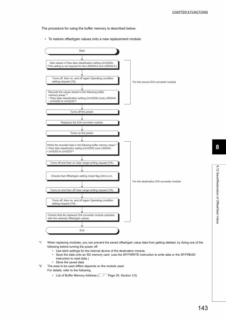
CHAPTER 8 FUNCTIONS
8
8.1
2 S
ave
/Re
stora
tion
of O
ffset/G
ain
Va
lue
The procedure for using the buffer memory is described below.
• To restore offset/gain values onto a new replacement module:
*1 When replacing modules, you can prevent the saved offset/gain value data from getting deleted, by doing one of the following before turning the power off:
• Use latch settings for the internal device of the destination module.• Save the data onto an SD memory card. (use the SP.FWRITE instruction to write data or the SP.FREAD
instruction to read data.)• Store the saved data
*2 The area to be used differs depends on the module used.For details, refer to the following.
• List of Buffer Memory Address ( Page 30, Section 3.5)
Records the values stored in the following buffer memory areas.*1
• Pass data classification setting (Un\G200) (only L60DA4)• Un\G202 to Un\G233*2
Replaces the D/A converter module.
Turns off and then on User range writing request (YA).
Checks that Offset/gain setting mode flag (XA) is on.
Turns on and then off User range writing request (YA).
Checks that the replaced D/A converter module operates with the restored offset/gain values.
End
Writes the recorded data in the following buffer memory areas.*1
• Pass data classification setting (Un\G200) (only L60DA4)• Un\G202 to Un\G233*2
Turns off the power.
Turns on the power.
Start
Sets values in Pass data classification setting (Un\G200). (This setting is not required for the L60DAVL8 and L60DAIL8.)
Turns off, then on, and off again Operating condition setting request (Y9).
Turns off, then on, and off again Operating condition setting request (Y9).
For the destination D/A converter module
For the source D/A converter module
143
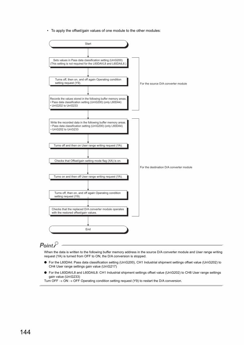
• To apply the offset/gain values of one module to the other modules:
When the data is written to the following buffer memory address in the source D/A converter module and User range writing request (YA) is turned from OFF to ON, the D/A conversion is stopped.
● For the L60DA4: Pass data classification setting (Un\G200), CH1 Industrial shipment settings offset value (Un\G202) to CH4 User range settings gain value (Un\G217)
● For the L60DAVL8 and L60DAIL8: CH1 Industrial shipment settings offset value (Un\G202) to CH8 User range settings gain value (Un\G233)
Turn OFF ON OFF Operating condition setting request (Y9) to restart the D/A conversion.
End
For the destination D/A converter module
Start
For the source D/A converter module
Records the values stored in the following buffer memory areas.• Pass data classification setting (Un\G200) (only L60DA4)• Un\G202 to Un\G233
Turns off and then on User range writing request (YA).
Checks that Offset/gain setting mode flag (XA) is on.
Turns on and then off User range writing request (YA).
Checks that the replaced D/A converter module operates with the restored offset/gain values.
Write the recorded data in the following buffer memory areas.• Pass data classification setting (Un\G200) (only L60DA4) • Un\G202 to Un\G233
Sets values in Pass data classification setting (Un\G200).(This setting is not required for the L60DAVL8 and L60DAIL8.)
Turns off, then on, and off again Operating condition setting request (Y9).
Turns off, then on, and off again Operating condition setting request (Y9).
144
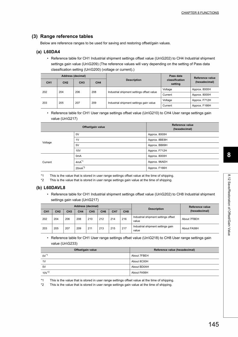
CHAPTER 8 FUNCTIONS
8
8.1
2 S
ave
/Re
stora
tion
of O
ffset/G
ain
Va
lue
(3) Range reference tablesBelow are reference ranges to be used for saving and restoring offset/gain values.
(a) L60DA4
• Reference table for CH1 Industrial shipment settings offset value (Un\G202) to CH4 Industrial shipment
settings gain value (Un\G209) (The reference values will vary depending on the setting of Pass data
classification setting (Un\G200) (voltage or current).)
• Reference table for CH1 User range settings offset value (Un\G210) to CH4 User range settings gain
value (Un\G217)
*1 This is the value that is stored in user range settings offset value at the time of shipping.*2 This is the value that is stored in user range settings gain value at the time of shipping.
(b) L60DAVL8
• Reference table for CH1 Industrial shipment settings offset value (Un\G202) to CH8 Industrial shipment
settings gain value (Un\G217)
• Reference table for CH1 User range settings offset value (Un\G218) to CH8 User range settings gain
value (Un\G233)
*1 This is the value that is stored in user range settings offset value at the time of shipping.*2 This is the value that is stored in user range settings gain value at the time of shipping.
Address (decimal)
Description
Pass data
classification
setting
Reference value
(hexadecimal)CH1 CH2 CH3 CH4
202 204 206 208 Industrial shipment settings offset valueVoltage Approx. 8000H
Current Approx. 8000H
203 205 207 209 Industrial shipment settings gain valueVoltage Approx. F712H
Current Approx. F166H
Offset/gain valueReference value
(hexadecimal)
Voltage
0V Approx. 8000H
1V Approx. 8BE8H
5V Approx. BB89H
10V Approx. F712H
Current
0mA Approx. 8000H
4mA*1 Approx. 96AEH
20mA*2 Approx. F166H
Address (decimal)Description
Reference value
(hexadecimal)CH1 CH2 CH3 CH4 CH5 CH6 CH7 CH8
202 204 206 208 210 212 214 216Industrial shipment settings offset
valueAbout 7FBEH
203 205 207 209 211 213 215 217Industrial shipment settings gain
valueAbout FA56H
Offset/gain value Reference value (hexadecimal)
0V*1 About 7FBEH
1V About 8C00H
5V About BD0AH
10V*2 About FA56H
145
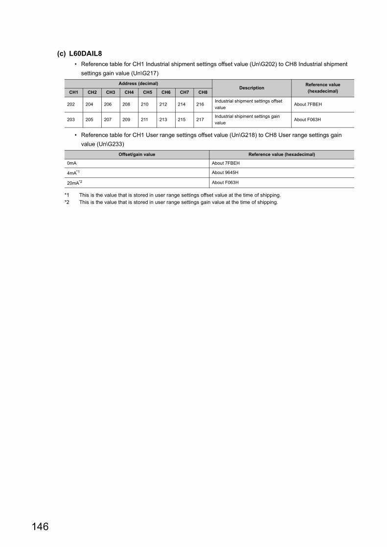
(c) L60DAIL8
• Reference table for CH1 Industrial shipment settings offset value (Un\G202) to CH8 Industrial shipment
settings gain value (Un\G217)
• Reference table for CH1 User range settings offset value (Un\G218) to CH8 User range settings gain
value (Un\G233)
*1 This is the value that is stored in user range settings offset value at the time of shipping.*2 This is the value that is stored in user range settings gain value at the time of shipping.
Address (decimal)Description
Reference value
(hexadecimal)CH1 CH2 CH3 CH4 CH5 CH6 CH7 CH8
202 204 206 208 210 212 214 216Industrial shipment settings offset
valueAbout 7FBEH
203 205 207 209 211 213 215 217Industrial shipment settings gain
valueAbout F063H
Offset/gain value Reference value (hexadecimal)
0mA About 7FBEH
4mA*1 About 9645H
20mA*2 About F063H
146
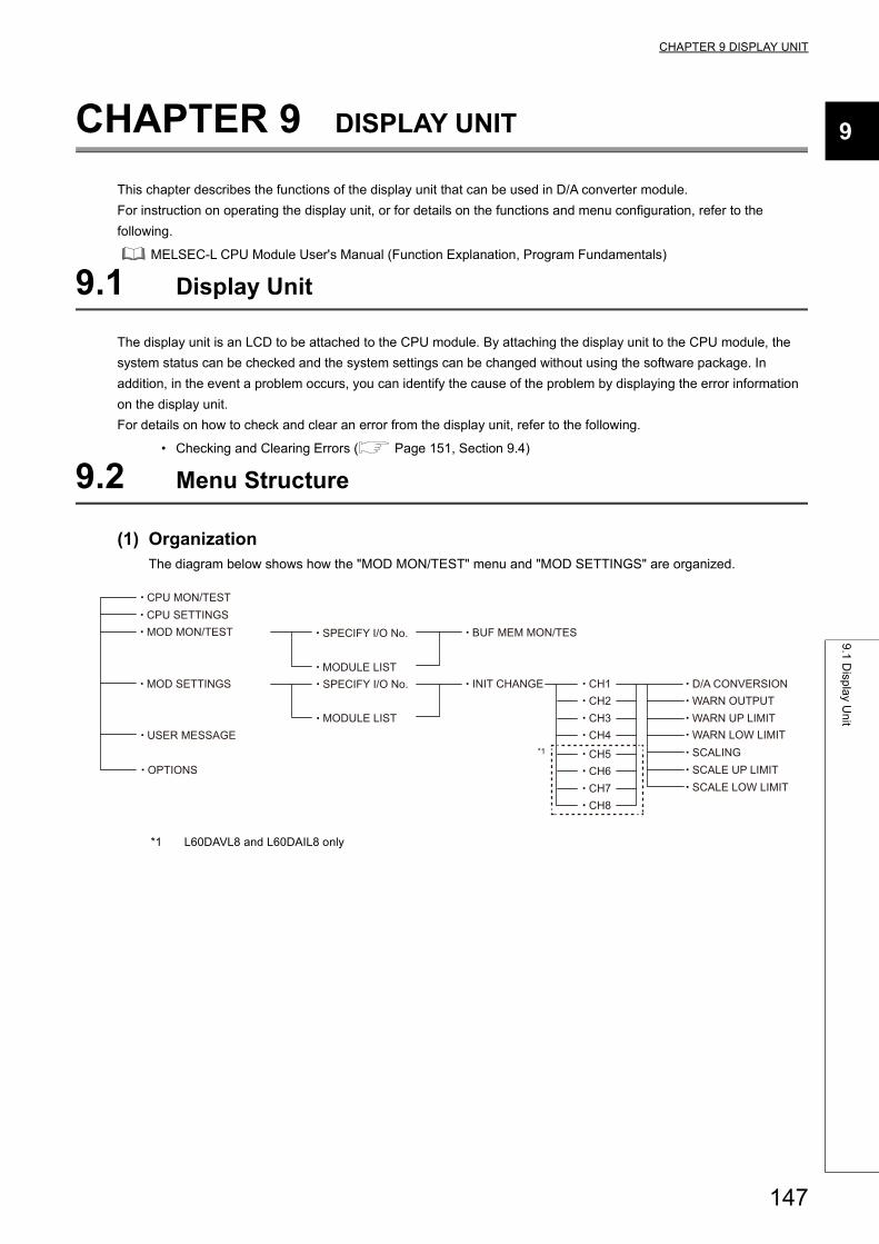
CHAPTER 9 DISPLAY UNIT
9
9.1
Disp
lay U
nit
CHAPTER 9 DISPLAY UNIT
This chapter describes the functions of the display unit that can be used in D/A converter module.
For instruction on operating the display unit, or for details on the functions and menu configuration, refer to the
following.
MELSEC-L CPU Module User's Manual (Function Explanation, Program Fundamentals)
9.1 Display Unit
The display unit is an LCD to be attached to the CPU module. By attaching the display unit to the CPU module, the
system status can be checked and the system settings can be changed without using the software package. In
addition, in the event a problem occurs, you can identify the cause of the problem by displaying the error information
on the display unit.
For details on how to check and clear an error from the display unit, refer to the following.
• Checking and Clearing Errors ( Page 151, Section 9.4)
9.2 Menu Structure
(1) OrganizationThe diagram below shows how the "MOD MON/TEST" menu and "MOD SETTINGS" are organized.
*1 L60DAVL8 and L60DAIL8 only
CPU SETTINGSBUF MEM MON/TES
CH1CH2CH3CH4
CH5CH6CH7CH8
SCALING
MOD SETTINGS
USER MESSAGE
OPTIONS
*1
CPU MON/TEST
MOD MON/TEST SPECIFY I/O No.
MODULE LISTSPECIFY I/O No.
MODULE LIST
INIT CHANGE D/A CONVERSIONWARN OUTPUTWARN UP LIMITWARN LOW LIMIT
SCALE UP LIMITSCALE LOW LIMIT
147
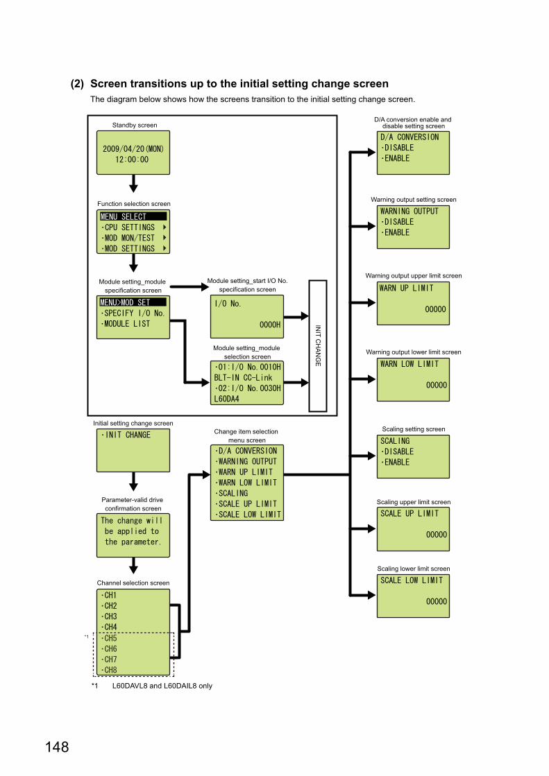
(2) Screen transitions up to the initial setting change screenThe diagram below shows how the screens transition to the initial setting change screen.
*1 L60DAVL8 and L60DAIL8 only
Module setting_module specification screen
Change item selection menu screen
Channel selection screen
Module setting_module selection screen
Module setting_start I/O No. specification screen
Standby screen
Function selection screen
D/A conversion enable and disable setting screen
Warning output setting screen
Warning output lower limit screen
Scaling setting screen
Scaling upper limit screen
Scaling lower limit screen
Warning output upper limit screen
INIT C
HA
NG
E
Initial setting change screen
Parameter-valid drive confirmation screen
*1
148
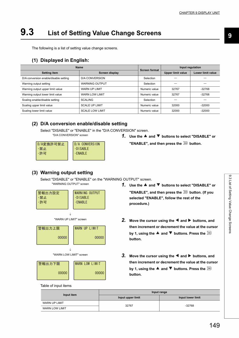
CHAPTER 9 DISPLAY UNIT
9
9.3
List o
f Se
tting
Va
lue
Ch
an
ge
Scre
en
s
9.3 List of Setting Value Change Screens
The following is a list of setting value change screens.
(1) Displayed in English:
(2) D/A conversion enable/disable settingSelect "DISABLE" or "ENABLE" in the "D/A CONVERSION" screen.
(3) Warning output settingSelect "DISABLE" or "ENABLE" on the "WARNING OUTPUT" screen.
Table of input items
NameScreen format
Input regulation
Setting item Screen display Upper limit value Lower limit value
D/A conversion enable/disable setting D/A CONVERSION Selection
Warning output setting WARNING OUTPUT Selection
Warning output upper limit value WARN UP LIMIT Numeric value 32767 -32768
Warning output lower limit value WARN LOW LIMIT Numeric value 32767 -32768
Scaling enable/disable setting SCALING Selection
Scaling upper limit value SCALE UP LIMIT Numeric value 32000 -32000
Scaling lower limit value SCALE LOW LIMIT Numeric value 32000 -32000
"D/A CONVERSION" screen 1. Use the and buttons to select "DISABLE" or
"ENABLE", and then press the button.
"WARNING OUTPUT" screen 1. Use the and buttons to select "DISABLE" or
"ENABLE", and then press the button. (If you
selected "ENABLE", follow the rest of the
procedure.)
"WARN UP LIMIT" screen 2. Move the cursor using the and buttons, and
then increment or decrement the value at the cursor
by 1, using the and buttons. Press the
button.
"WARN LOW LIMIT" screen 3. Move the cursor using the and buttons, and
then increment or decrement the value at the cursor
by 1, using the and buttons. Press the
button.
Input itemInput range
Input upper limit Input lower limit
WARN UP LIMIT32767 -32768
WARN LOW LIMIT
OK
OK
OK
OK
149
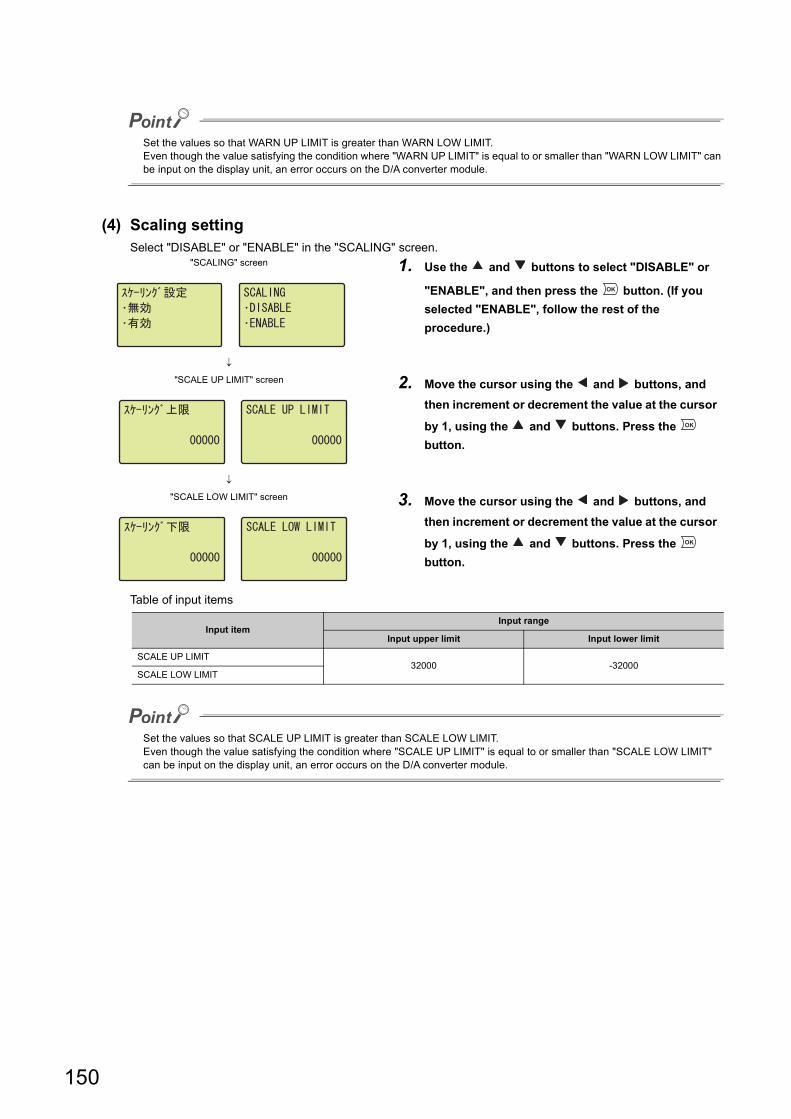
Set the values so that WARN UP LIMIT is greater than WARN LOW LIMIT.Even though the value satisfying the condition where "WARN UP LIMIT" is equal to or smaller than "WARN LOW LIMIT" can be input on the display unit, an error occurs on the D/A converter module.
(4) Scaling settingSelect "DISABLE" or "ENABLE" in the "SCALING" screen.
Table of input items
Set the values so that SCALE UP LIMIT is greater than SCALE LOW LIMIT.Even though the value satisfying the condition where "SCALE UP LIMIT" is equal to or smaller than "SCALE LOW LIMIT" can be input on the display unit, an error occurs on the D/A converter module.
"SCALING" screen 1. Use the and buttons to select "DISABLE" or
"ENABLE", and then press the button. (If you
selected "ENABLE", follow the rest of the
procedure.)
"SCALE UP LIMIT" screen 2. Move the cursor using the and buttons, and
then increment or decrement the value at the cursor
by 1, using the and buttons. Press the
button.
"SCALE LOW LIMIT" screen 3. Move the cursor using the and buttons, and
then increment or decrement the value at the cursor
by 1, using the and buttons. Press the
button.
Input itemInput range
Input upper limit Input lower limit
SCALE UP LIMIT32000 -32000
SCALE LOW LIMIT
OK
OK
OK
150
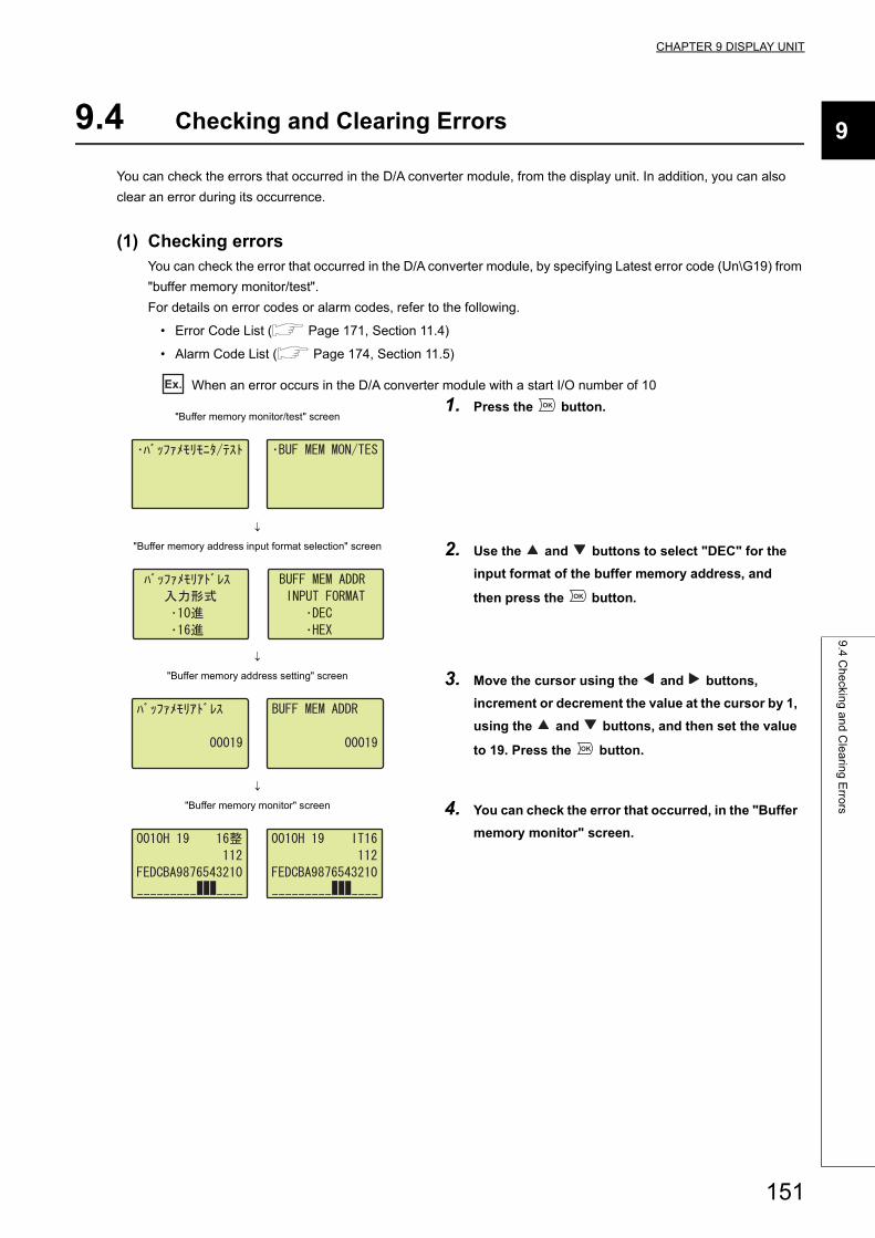
CHAPTER 9 DISPLAY UNIT
9
9.4
Ch
eckin
g a
nd
Cle
arin
g E
rrors
9.4 Checking and Clearing Errors
You can check the errors that occurred in the D/A converter module, from the display unit. In addition, you can also
clear an error during its occurrence.
(1) Checking errorsYou can check the error that occurred in the D/A converter module, by specifying Latest error code (Un\G19) from
"buffer memory monitor/test".
For details on error codes or alarm codes, refer to the following.
• Error Code List ( Page 171, Section 11.4)
• Alarm Code List ( Page 174, Section 11.5)
Ex. When an error occurs in the D/A converter module with a start I/O number of 10
"Buffer memory monitor/test" screen1. Press the button.
"Buffer memory address input format selection" screen 2. Use the and buttons to select "DEC" for the
input format of the buffer memory address, and
then press the button.
"Buffer memory address setting" screen 3. Move the cursor using the and buttons,
increment or decrement the value at the cursor by 1,
using the and buttons, and then set the value
to 19. Press the button.
"Buffer memory monitor" screen 4. You can check the error that occurred, in the "Buffer
memory monitor" screen.
OK
OK
OK
151
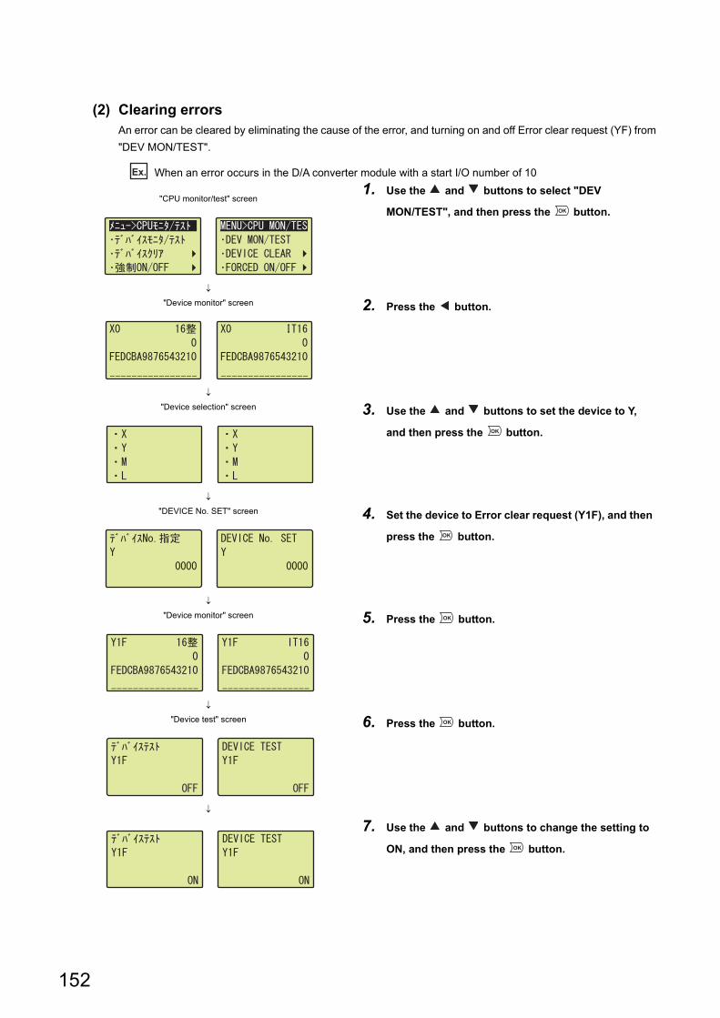
(2) Clearing errorsAn error can be cleared by eliminating the cause of the error, and turning on and off Error clear request (YF) from
"DEV MON/TEST".
Ex. When an error occurs in the D/A converter module with a start I/O number of 10
"CPU monitor/test" screen1. Use the and buttons to select "DEV
MON/TEST", and then press the button.
"Device monitor" screen 2. Press the button.
"Device selection" screen 3. Use the and buttons to set the device to Y,
and then press the button.
"DEVICE No. SET" screen 4. Set the device to Error clear request (Y1F), and then
press the button.
"Device monitor" screen 5. Press the button.
"Device test" screen 6. Press the button.
7. Use the and buttons to change the setting to
ON, and then press the button.
OK
OK
OK
OK
OK
OK
152
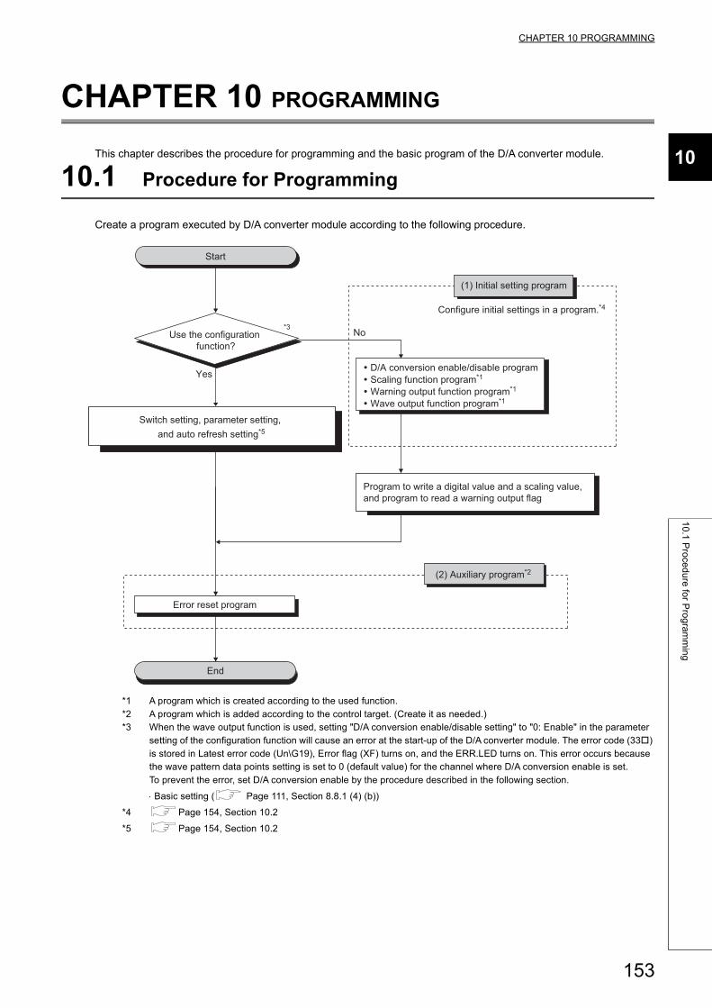
CHAPTER 10 PROGRAMMING
10
10
.1 P
roce
du
re fo
r Pro
gra
mm
ing
CHAPTER 10 PROGRAMMING
This chapter describes the procedure for programming and the basic program of the D/A converter module.
10.1 Procedure for Programming
Create a program executed by D/A converter module according to the following procedure.
*1 A program which is created according to the used function.*2 A program which is added according to the control target. (Create it as needed.)*3 When the wave output function is used, setting "D/A conversion enable/disable setting" to "0: Enable" in the parameter
setting of the configuration function will cause an error at the start-up of the D/A converter module. The error code (33) is stored in Latest error code (Un\G19), Error flag (XF) turns on, and the ERR.LED turns on. This error occurs because the wave pattern data points setting is set to 0 (default value) for the channel where D/A conversion enable is set.To prevent the error, set D/A conversion enable by the procedure described in the following section.
Basic setting ( Page 111, Section 8.8.1 (4) (b))
*4 Page 154, Section 10.2
*5 Page 154, Section 10.2
No
Yes
Start
End
� D/A conversion enable/disable program� Scaling function program*1
� Warning output function program*1
� Wave output function program*1
Switch setting, parameter setting, and auto refresh setting*5
Error reset program
Use the configuration function?
(1) Initial setting program
(2) Auxiliary program*2
Configure initial settings in a program.*4
Program to write a digital value and a scaling value, and program to read a warning output flag
*3
153
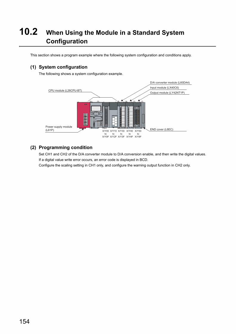
10.2 When Using the Module in a Standard System Configuration
This section shows a program example where the following system configuration and conditions apply.
(1) System configurationThe following shows a system configuration example.
(2) Programming conditionSet CH1 and CH2 of the D/A converter module to D/A conversion enable, and then write the digital values.
If a digital value write error occurs, an error code is displayed in BCD.
Configure the scaling setting in CH1 only, and configure the warning output function in CH2 only.
CPU module (L26CPU-BT)
Power supply module (L61P)
Input module (LX40C6)
Output module (LY42NT1P)
D/A converter module (L60DA4)
END cover (L6EC)X/Y00to
X/Y0F
X/Y30to
X/Y3F
X/Y40to
X/Y4F
X/Y50to
X/Y8F
X/Y10to
X/Y2F
154
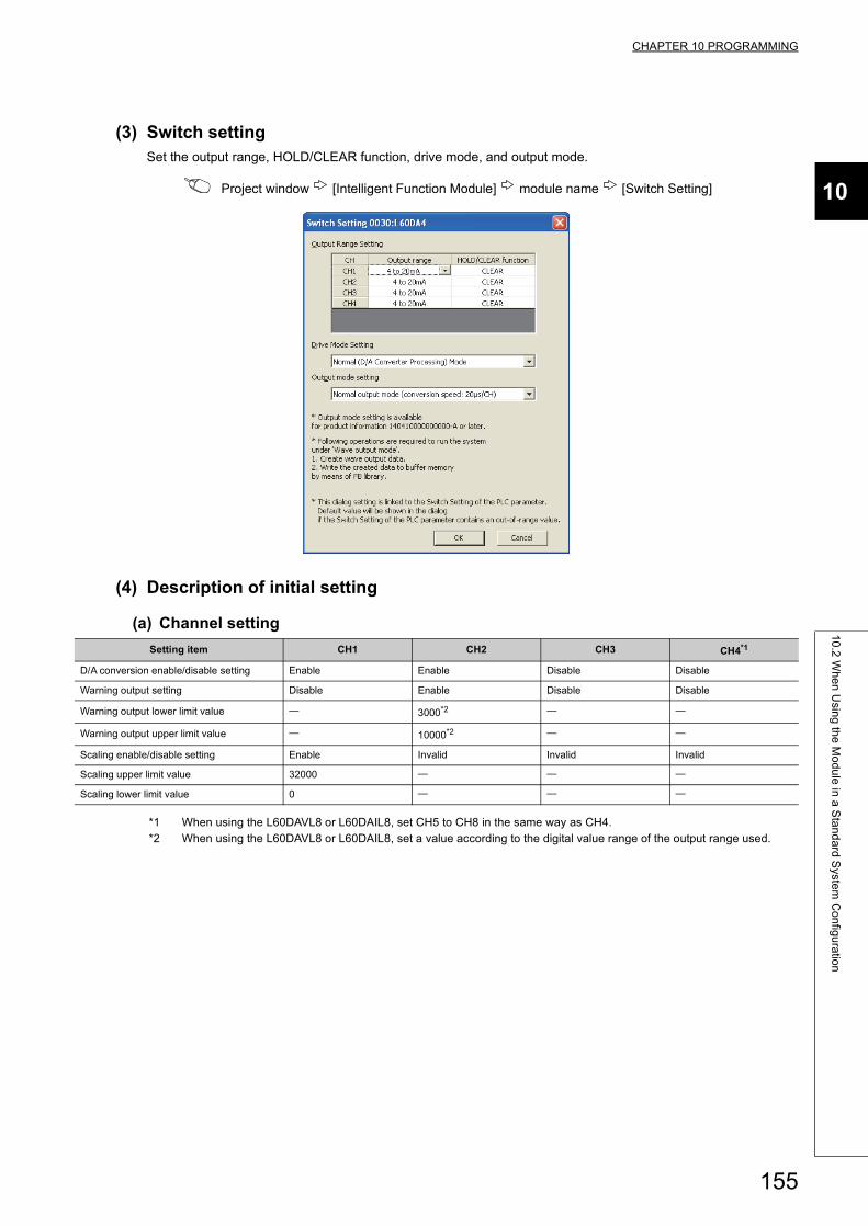
CHAPTER 10 PROGRAMMING
10
10
.2 W
he
n U
sing
the
Mo
du
le in
a S
tan
da
rd S
ystem
Co
nfig
ura
tion
(3) Switch settingSet the output range, HOLD/CLEAR function, drive mode, and output mode.
Project window [Intelligent Function Module] module name [Switch Setting]
(4) Description of initial setting
(a) Channel setting
*1 When using the L60DAVL8 or L60DAIL8, set CH5 to CH8 in the same way as CH4.*2 When using the L60DAVL8 or L60DAIL8, set a value according to the digital value range of the output range used.
Setting item CH1 CH2 CH3 CH4*1
D/A conversion enable/disable setting Enable Enable Disable Disable
Warning output setting Disable Enable Disable Disable
Warning output lower limit value 3000*2
Warning output upper limit value 10000*2
Scaling enable/disable setting Enable Invalid Invalid Invalid
Scaling upper limit value 32000
Scaling lower limit value 0
155
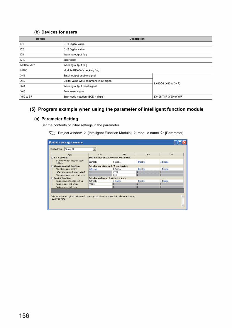
(b) Devices for users
(5) Program example when using the parameter of intelligent function module
(a) Parameter Setting
Set the contents of initial settings in the parameter.
Project window [Intelligent Function Module] module name [Parameter]
Device Description
D1 CH1 Digital value
D2 CH2 Digital value
D8 Warning output flag
D10 Error code
M20 to M27 Warning output flag
M100 Module READY checking flag
X41 Batch output enable signal
LX40C6 (X40 to X4F)X42 Digital value write command input signal
X44 Warning output reset signal
X45 Error reset signal
Y50 to 5F Error code notation (BCD 4 digits) LY42NT1P (Y50 to Y5F)
156
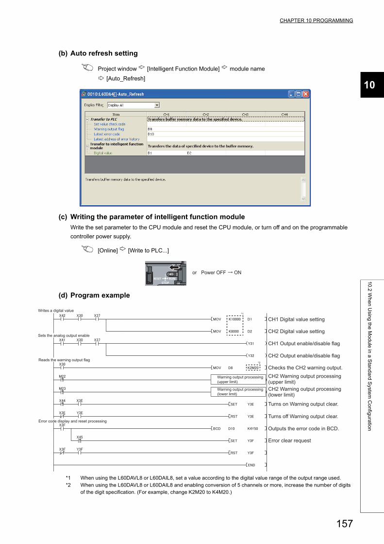
CHAPTER 10 PROGRAMMING
10
10
.2 W
he
n U
sing
the
Mo
du
le in
a S
tan
da
rd S
ystem
Co
nfig
ura
tion
(b) Auto refresh setting
Project window [Intelligent Function Module] module name
[Auto_Refresh]
(c) Writing the parameter of intelligent function module
Write the set parameter to the CPU module and reset the CPU module, or turn off and on the programmable
controller power supply.
[Online] [Write to PLC...]
(d) Program example
*1 When using the L60DAVL8 or L60DAIL8, set a value according to the digital value range of the output range used.*2 When using the L60DAVL8 or L60DAIL8 and enabling conversion of 5 channels or more, increase the number of digits
of the digit specification. (For example, change K2M20 to K4M20.)
or Power OFF ON
CH1 Digital value setting
CH2 Digital value setting
CH1 Output enable/disable flag
CH2 Output enable/disable flag
Checks the CH2 warning output.CH2 Warning output processing (upper limit)CH2 Warning output processing (lower limit)
Turns on Warning output clear.
Turns off Warning output clear.
Outputs the error code in BCD.
Error clear request
Warning output processing (upper limit)
Warning output processing (lower limit)
Writes a digital value
Sets the analog output enable
Reads the warning output flag
Error code display and reset processing
*1
*2
157
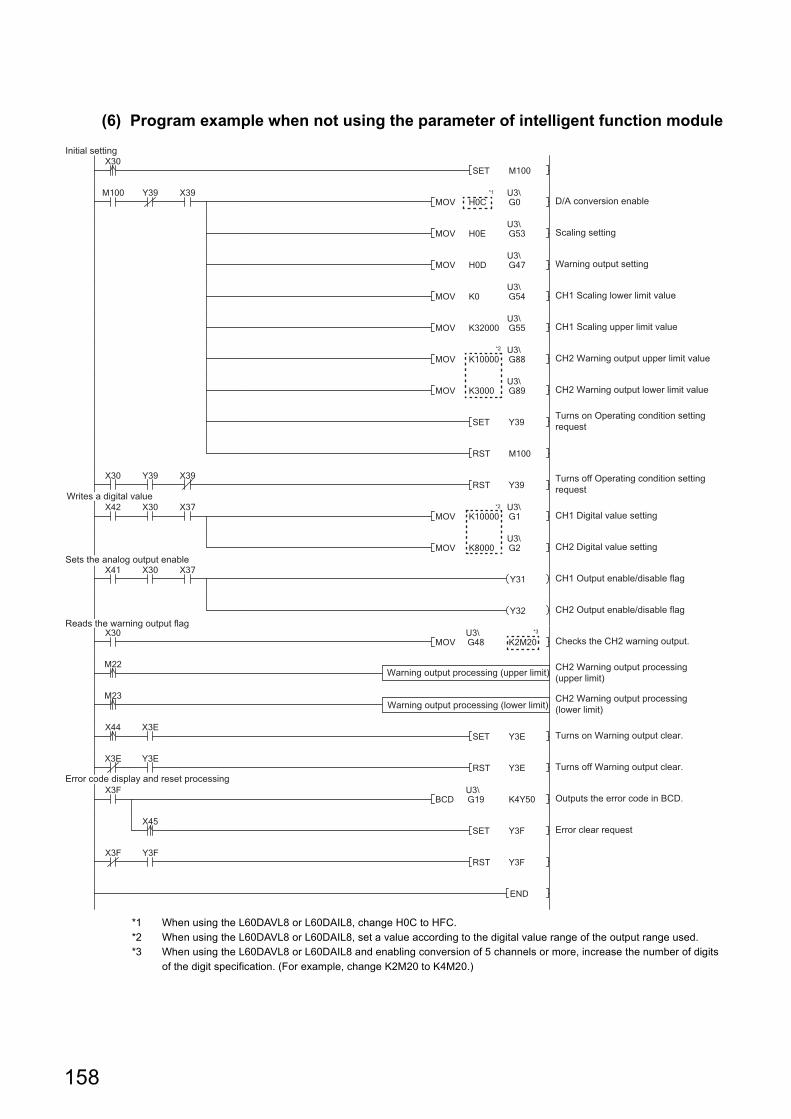
(6) Program example when not using the parameter of intelligent function module
*1 When using the L60DAVL8 or L60DAIL8, change H0C to HFC.*2 When using the L60DAVL8 or L60DAIL8, set a value according to the digital value range of the output range used.*3 When using the L60DAVL8 or L60DAIL8 and enabling conversion of 5 channels or more, increase the number of digits
of the digit specification. (For example, change K2M20 to K4M20.)
Warning output processing (upper limit)
Initial setting
Writes a digital value
Sets the analog output enable
Error code display and reset processing
Reads the warning output flag
D/A conversion enable
Scaling setting
Warning output setting
CH1 Scaling lower limit value
CH1 Scaling upper limit value
CH2 Warning output upper limit value
CH2 Warning output lower limit value
Turns on Operating condition setting request
Turns off Operating condition setting request
CH1 Digital value setting
CH2 Digital value setting
CH1 Output enable/disable flag
CH2 Output enable/disable flag
Checks the CH2 warning output.
CH2 Warning output processing(upper limit)
CH2 Warning output processing (lower limit)
Turns on Warning output clear.
Turns off Warning output clear.
Outputs the error code in BCD.
Error clear request
*1
*2
*2
*3
Warning output processing (lower limit)
158
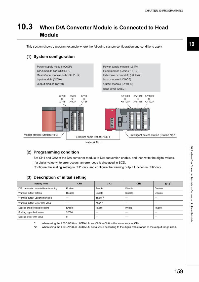
CHAPTER 10 PROGRAMMING
10
10
.3 W
he
n D
/A C
on
verte
r Mo
du
le is C
on
ne
cted
to H
ea
d M
od
ule
10.3 When D/A Converter Module is Connected to Head Module
This section shows a program example where the following system configuration and conditions apply.
(1) System configuration
(2) Programming conditionSet CH1 and CH2 of the D/A converter module to D/A conversion enable, and then write the digital values.
If a digital value write error occurs, an error code is displayed in BCD.
Configure the scaling setting in CH1 only, and configure the warning output function in CH2 only.
(3) Description of initial setting
*1 When using the L60DAVL8 or L60DAIL8, set CH5 to CH8 in the same way as CH4.*2 When using the L60DAVL8 or L60DAIL8, set a value according to the digital value range of the output range used.
Setting item CH1 CH2 CH3 CH4*1
D/A conversion enable/disable setting Enable Enable Disable Disable
Warning output setting Disable Enable Disable Disable
Warning output upper limit value 10000*2
Warning output lower limit value 3000*2
Scaling enable/disable setting Enable Invalid Invalid Invalid
Scaling upper limit value 32000
Scaling lower limit value 0
Network No.1
Ethernet cable (1000BASE-T)
CPU module (Q10UDHCPU)Master/local module (QJ71GF11-T2)Input module (QX10)
Output module (QY10)
X/Y1000to
X/Y100F
X/Y1010to
X/Y101F
X/Y1020to
X/Y102F
Master station (Station No.0) Intelligent device station (Station No.1)
Head module (LJ72GF15-T2)D/A converter module (L60DA4)Input module (LX40C6)
Output module (LY10R2)
END cover (L6EC)
Power supply module (Q62P) Power supply module (L61P)
X/Y00to
X/Y1F
X/Y20to
X/Y2F
X/Y30to
X/Y3F
159
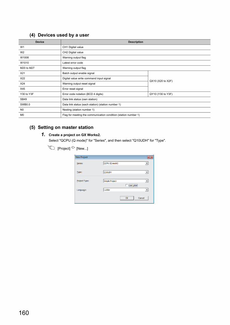
(4) Devices used by a user
(5) Setting on master station
1. Create a project on GX Works2.
Select "QCPU (Q mode)" for "Series", and then select "Q10UDH" for "Type".
[Project] [New...]
Device Description
W1 CH1 Digital value
W2 CH2 Digital value
W1008 Warning output flag
W1010 Latest error code
M20 to M27 Warning output flag
X21 Batch output enable signal
QX10 (X20 to X2F)X22 Digital value write command input signal
X24 Warning output reset signal
X45 Error reset signal
Y30 to Y3F Error code notation (BCD 4 digits) QY10 (Y30 to Y3F)
SB49 Data link status (own station)
SWB0.0 Data link status (each station) (station number 1)
N0 Nesting (station number 1)
M0 Flag for meeting the communication condition (station number 1)
160
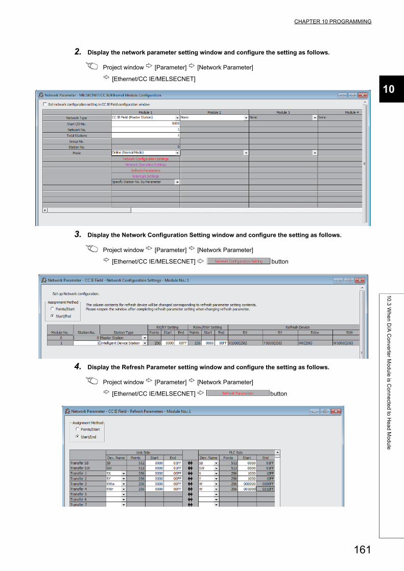
CHAPTER 10 PROGRAMMING
10
10
.3 W
he
n D
/A C
on
verte
r Mo
du
le is C
on
ne
cted
to H
ea
d M
od
ule
2. Display the network parameter setting window and configure the setting as follows.
Project window [Parameter] [Network Parameter]
[Ethernet/CC IE/MELSECNET]
3. Display the Network Configuration Setting window and configure the setting as follows.
Project window [Parameter] [Network Parameter]
[Ethernet/CC IE/MELSECNET] button
4. Display the Refresh Parameter setting window and configure the setting as follows.
Project window [Parameter] [Network Parameter]
[Ethernet/CC IE/MELSECNET] button
161
5. Write the set parameter to the CPU module of the master station and reset the CPU module, or turn
off and on the programmable controller power supply.
[Online] [Write to PLC...]
or Power OFF ON
162
CHAPTER 10 PROGRAMMING
10
10
.3 W
he
n D
/A C
on
verte
r Mo
du
le is C
on
ne
cted
to H
ea
d M
od
ule
(6) Setting on intelligent device station
1. Create a project on GX Works2.
Select "LCPU" for "Series", and then select "LJ72GF15-T2" for "Type".
[Project] [New...]
2. Display the PLC Parameter setting window and configure the setting as follows.
Project window [Parameter] [PLC Parameter] "Communication Head Setting"
163
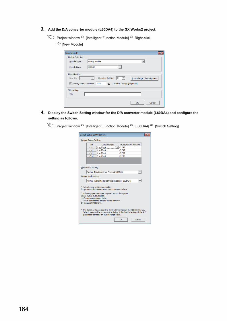
3. Add the D/A converter module (L60DA4) to the GX Works2 project.
Project window [Intelligent Function Module] Right-click
[New Module]
4. Display the Switch Setting window for the D/A converter module (L60DA4) and configure the
setting as follows.
Project window [Intelligent Function Module] [L60DA4] [Switch Setting]
164
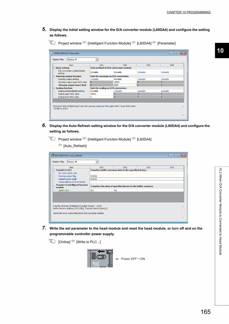
CHAPTER 10 PROGRAMMING
10
10
.3 W
he
n D
/A C
on
verte
r Mo
du
le is C
on
ne
cted
to H
ea
d M
od
ule
5. Display the initial setting window for the D/A converter module (L60DA4) and configure the setting
as follows.
Project window [Intelligent Function Module] [L60DA4] [Parameter]
6. Display the Auto Refresh setting window for the D/A converter module (L60DA4) and configure the
setting as follows.
Project window [Intelligent Function Module] [L60DA4]
[Auto_Refresh]
7. Write the set parameter to the head module and reset the head module, or turn off and on the
programmable controller power supply.
[Online] [Write to PLC...]
or Power OFF ON
165
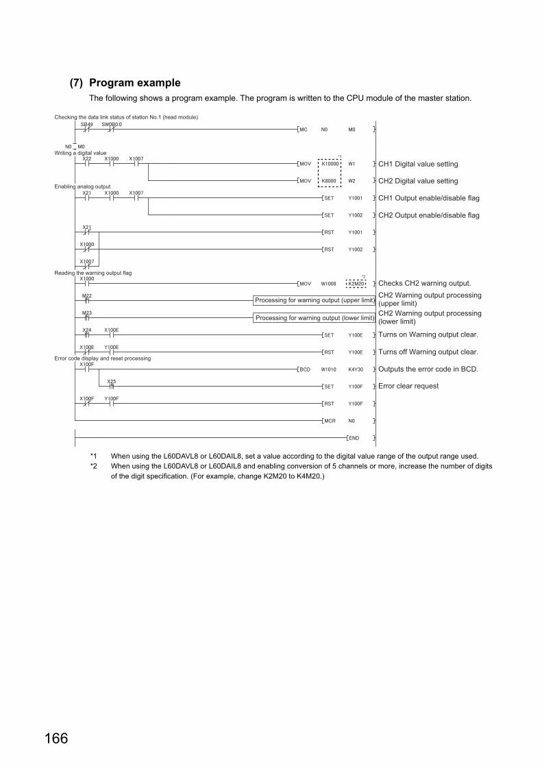
(7) Program exampleThe following shows a program example. The program is written to the CPU module of the master station.
*1 When using the L60DAVL8 or L60DAIL8, set a value according to the digital value range of the output range used.*2 When using the L60DAVL8 or L60DAIL8 and enabling conversion of 5 channels or more, increase the number of digits
of the digit specification. (For example, change K2M20 to K4M20.)
CH1 Digital value setting
CH2 Digital value setting
CH1 Output enable/disable flag
CH2 Output enable/disable flag
Checks CH2 warning output.CH2 Warning output processing (upper limit)CH2 Warning output processing (lower limit)
Turns on Warning output clear.
Turns off Warning output clear.
Outputs the error code in BCD.
Error clear request
Processing for warning output (upper limit)
Processing for warning output (lower limit)
Checking the data link status of station No.1 (head module)
Writing a digital value
Enabling analog output
Reading the warning output flag
Error code display and reset processing
*1
*2
166
CHAPTER 11 TROUBLESHOOTING
11
CHAPTER 11 TROUBLESHOOTING
This chapter describes errors that may occur while using the D/A converter module, and those troubleshooting.
(1) Checking for the error codes and the alarm codesErrors and alarms occurred in the D/A converter module can be checked with the following methods.
Check according to the purpose and application.
• Checking on the Module Detailed Information ( Page 168, Section 11.1)
• Checking by Latest Error Code (Un\G19) ( Page 169, Section 11.2)
• Checking on the Module Error Collection Function ( Page 170, Section 11.3)
• Checking by a display unit ( Page 151, Section 9.4)
167
11.1 Checking on the Module Detailed Information
The following describes how to check the errors on the module detailed information.
[Diagnostics] [System Monitor...]
1. Select the D/A converter module in "Main
Block" and click the
button.
2. "Module's Detailed Information" of the
D/A converter module is displayed.
168
CHAPTER 11 TROUBLESHOOTING
11
11
.2 C
he
cking
by L
ate
st Erro
r Co
de
(Un
\G1
9)
11.2 Checking by Latest Error Code (Un\G19)
The following describes how to check the error codes and alarm codes in Latest error code (Un\G19).
[Online] [Monitor] [Device/Buffer Memory Batch]
When multiple errors or warnings occur, the latest error code or alarm code is stored in Latest error code (Un\G19).
169
11.3 Checking on the Module Error Collection Function
By using the module error collection function, the errors occurred in the D/A converter module can be saved in the
CPU module. The error information can be held even after the CPU module is powered off and on or is reset.
(1) How to check the errors by the module error collection functionTo check the errors of the D/A converter module collected by the CPU module, open the "Error History" window.
[Diagnostics] [System Monitor...] click the button.
(2) Errors to be collectedThe D/A converter module reports the following information to the CPU module:
• Error Code List ( Page 171, Section 11.4)
• Alarm Code List ( Page 174, Section 11.5)
170
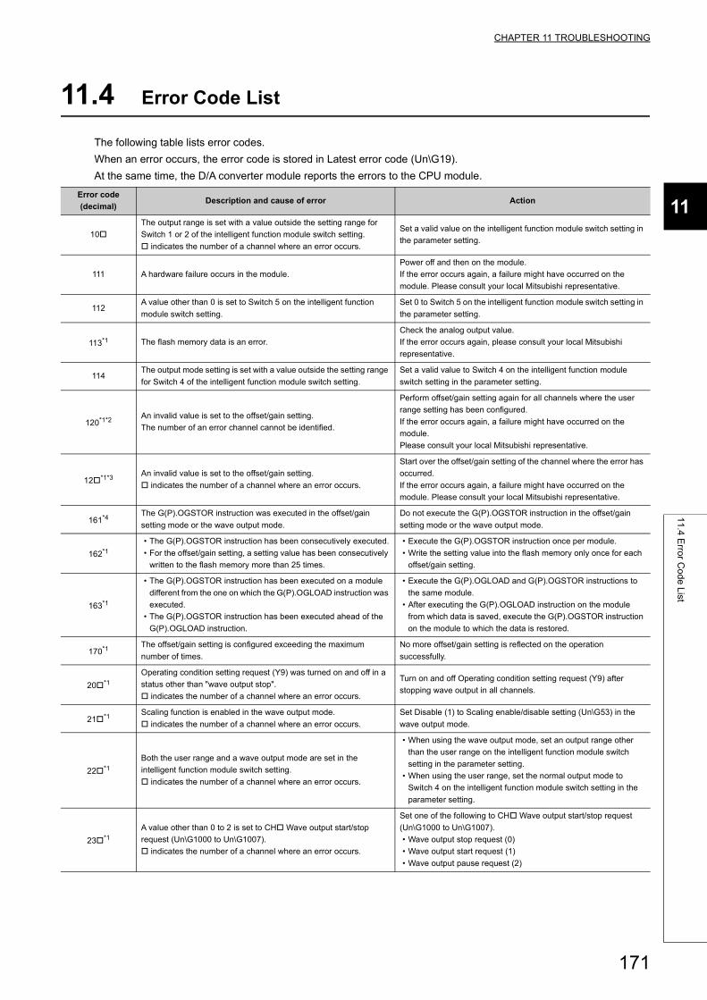
CHAPTER 11 TROUBLESHOOTING
11
11
.4 E
rror C
od
e L
ist
11.4 Error Code List
The following table lists error codes.
When an error occurs, the error code is stored in Latest error code (Un\G19).
At the same time, the D/A converter module reports the errors to the CPU module.
Error code
(decimal)Description and cause of error Action
10
The output range is set with a value outside the setting range for
Switch 1 or 2 of the intelligent function module switch setting.
indicates the number of a channel where an error occurs.
Set a valid value on the intelligent function module switch setting in
the parameter setting.
111 A hardware failure occurs in the module.
Power off and then on the module.
If the error occurs again, a failure might have occurred on the
module. Please consult your local Mitsubishi representative.
112A value other than 0 is set to Switch 5 on the intelligent function
module switch setting.
Set 0 to Switch 5 on the intelligent function module switch setting in
the parameter setting.
113*1 The flash memory data is an error.
Check the analog output value.
If the error occurs again, please consult your local Mitsubishi
representative.
114The output mode setting is set with a value outside the setting range
for Switch 4 of the intelligent function module switch setting.
Set a valid value to Switch 4 on the intelligent function module
switch setting in the parameter setting.
120*1*2An invalid value is set to the offset/gain setting.
The number of an error channel cannot be identified.
Perform offset/gain setting again for all channels where the user
range setting has been configured.
If the error occurs again, a failure might have occurred on the
module.
Please consult your local Mitsubishi representative.
12*1*3An invalid value is set to the offset/gain setting.
indicates the number of a channel where an error occurs.
Start over the offset/gain setting of the channel where the error has
occurred.
If the error occurs again, a failure might have occurred on the
module. Please consult your local Mitsubishi representative.
161*4The G(P).OGSTOR instruction was executed in the offset/gain
setting mode or the wave output mode.
Do not execute the G(P).OGSTOR instruction in the offset/gain
setting mode or the wave output mode.
162*1
• The G(P).OGSTOR instruction has been consecutively executed.
• For the offset/gain setting, a setting value has been consecutively
written to the flash memory more than 25 times.
• Execute the G(P).OGSTOR instruction once per module.
• Write the setting value into the flash memory only once for each
offset/gain setting.
163*1
• The G(P).OGSTOR instruction has been executed on a module
different from the one on which the G(P).OGLOAD instruction was
executed.
• The G(P).OGSTOR instruction has been executed ahead of the
G(P).OGLOAD instruction.
• Execute the G(P).OGLOAD and G(P).OGSTOR instructions to
the same module.
• After executing the G(P).OGLOAD instruction on the module
from which data is saved, execute the G(P).OGSTOR instruction
on the module to which the data is restored.
170*1The offset/gain setting is configured exceeding the maximum
number of times.
No more offset/gain setting is reflected on the operation
successfully.
20*1
Operating condition setting request (Y9) was turned on and off in a
status other than "wave output stop".
indicates the number of a channel where an error occurs.
Turn on and off Operating condition setting request (Y9) after
stopping wave output in all channels.
21*1Scaling function is enabled in the wave output mode.
indicates the number of a channel where an error occurs.
Set Disable (1) to Scaling enable/disable setting (Un\G53) in the
wave output mode.
22*1
Both the user range and a wave output mode are set in the
intelligent function module switch setting.
indicates the number of a channel where an error occurs.
• When using the wave output mode, set an output range other
than the user range on the intelligent function module switch
setting in the parameter setting.
• When using the user range, set the normal output mode to
Switch 4 on the intelligent function module switch setting in the
parameter setting.
23*1
A value other than 0 to 2 is set to CH Wave output start/stop
request (Un\G1000 to Un\G1007).
indicates the number of a channel where an error occurs.
Set one of the following to CH Wave output start/stop request
(Un\G1000 to Un\G1007).
• Wave output stop request (0)
• Wave output start request (1)
• Wave output pause request (2)
171
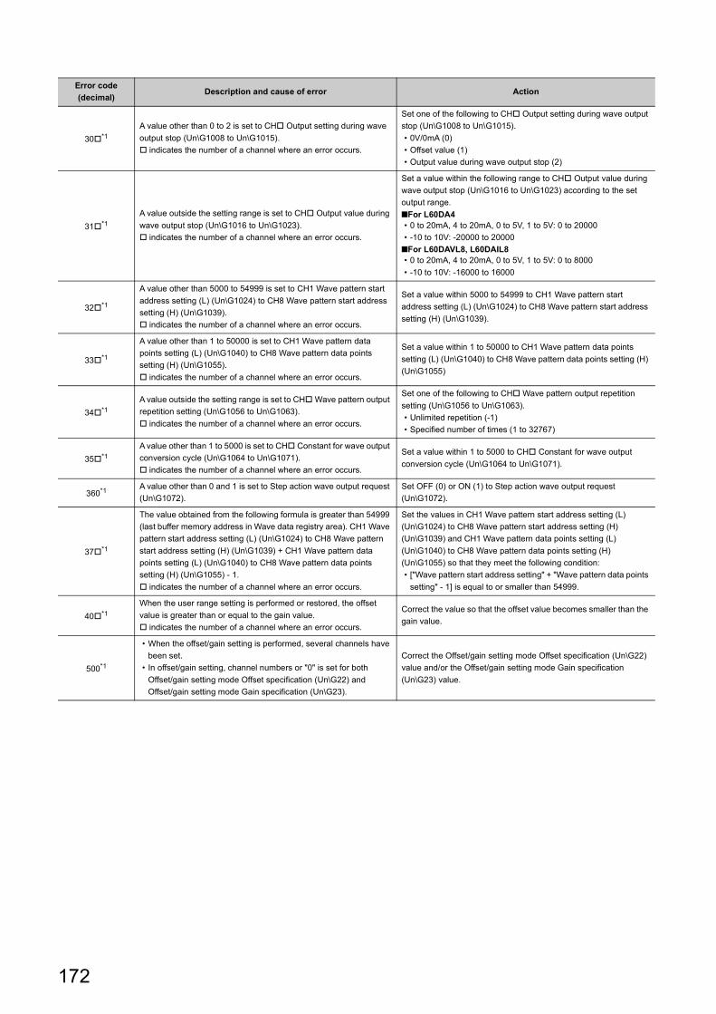
30*1
A value other than 0 to 2 is set to CH Output setting during wave
output stop (Un\G1008 to Un\G1015).
indicates the number of a channel where an error occurs.
Set one of the following to CH Output setting during wave output
stop (Un\G1008 to Un\G1015).
• 0V/0mA (0)
• Offset value (1)
• Output value during wave output stop (2)
31*1
A value outside the setting range is set to CH Output value during
wave output stop (Un\G1016 to Un\G1023).
indicates the number of a channel where an error occurs.
Set a value within the following range to CH Output value during
wave output stop (Un\G1016 to Un\G1023) according to the set
output range.
■For L60DA4• 0 to 20mA, 4 to 20mA, 0 to 5V, 1 to 5V: 0 to 20000
• -10 to 10V: -20000 to 20000
■For L60DAVL8, L60DAIL8• 0 to 20mA, 4 to 20mA, 0 to 5V, 1 to 5V: 0 to 8000
• -10 to 10V: -16000 to 16000
32*1
A value other than 5000 to 54999 is set to CH1 Wave pattern start
address setting (L) (Un\G1024) to CH8 Wave pattern start address
setting (H) (Un\G1039).
indicates the number of a channel where an error occurs.
Set a value within 5000 to 54999 to CH1 Wave pattern start
address setting (L) (Un\G1024) to CH8 Wave pattern start address
setting (H) (Un\G1039).
33*1
A value other than 1 to 50000 is set to CH1 Wave pattern data
points setting (L) (Un\G1040) to CH8 Wave pattern data points
setting (H) (Un\G1055).
indicates the number of a channel where an error occurs.
Set a value within 1 to 50000 to CH1 Wave pattern data points
setting (L) (Un\G1040) to CH8 Wave pattern data points setting (H)
(Un\G1055)
34*1
A value outside the setting range is set to CH Wave pattern output
repetition setting (Un\G1056 to Un\G1063).
indicates the number of a channel where an error occurs.
Set one of the following to CH Wave pattern output repetition
setting (Un\G1056 to Un\G1063).
• Unlimited repetition (-1)
• Specified number of times (1 to 32767)
35*1
A value other than 1 to 5000 is set to CH Constant for wave output
conversion cycle (Un\G1064 to Un\G1071).
indicates the number of a channel where an error occurs.
Set a value within 1 to 5000 to CH Constant for wave output
conversion cycle (Un\G1064 to Un\G1071).
360*1A value other than 0 and 1 is set to Step action wave output request
(Un\G1072).
Set OFF (0) or ON (1) to Step action wave output request
(Un\G1072).
37*1
The value obtained from the following formula is greater than 54999
(last buffer memory address in Wave data registry area). CH1 Wave
pattern start address setting (L) (Un\G1024) to CH8 Wave pattern
start address setting (H) (Un\G1039) + CH1 Wave pattern data
points setting (L) (Un\G1040) to CH8 Wave pattern data points
setting (H) (Un\G1055) - 1.
indicates the number of a channel where an error occurs.
Set the values in CH1 Wave pattern start address setting (L)
(Un\G1024) to CH8 Wave pattern start address setting (H)
(Un\G1039) and CH1 Wave pattern data points setting (L)
(Un\G1040) to CH8 Wave pattern data points setting (H)
(Un\G1055) so that they meet the following condition:
• ["Wave pattern start address setting" + "Wave pattern data points
setting" - 1] is equal to or smaller than 54999.
40*1
When the user range setting is performed or restored, the offset
value is greater than or equal to the gain value.
indicates the number of a channel where an error occurs.
Correct the value so that the offset value becomes smaller than the
gain value.
500*1
• When the offset/gain setting is performed, several channels have
been set.
• In offset/gain setting, channel numbers or "0" is set for both
Offset/gain setting mode Offset specification (Un\G22) and
Offset/gain setting mode Gain specification (Un\G23).
Correct the Offset/gain setting mode Offset specification (Un\G22)
value and/or the Offset/gain setting mode Gain specification
(Un\G23) value.
Error code
(decimal)Description and cause of error Action
172
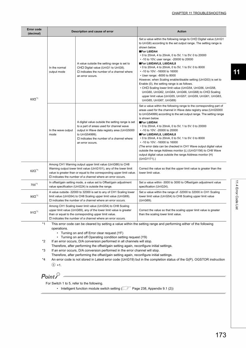
CHAPTER 11 TROUBLESHOOTING
11
11
.4 E
rror C
od
e L
ist
*1 This error code can be cleared by setting a value within the setting range and performing either of the following operations.
• Turning on and off Error clear request (YF)• Turning on and off Operating condition setting request (Y9)
*2 If an error occurs, D/A conversion performed in all channels will stop.Therefore, after performing the offset/gain setting again, reconfigure initial settings.
*3 If an error occurs, D/A conversion performed in the error channel will stop.Therefore, after performing the offset/gain setting again, reconfigure initial settings.
*4 An error code is not stored in Latest error code (Un\G19) but in the completion status of the G(P). OGSTOR instruction
+1.
For Switch 1 to 5, refer to the following.
• Intelligent function module switch setting ( Page 238, Appendix 9.1 (2))
60*1
In the normal
output mode
A value outside the setting range is set to
CH Digital value (Un\G1 to Un\G8).
indicates the number of a channel where
an error occurs.
Set a value within the following range to CH Digital value (Un\G1
to Un\G8) according to the set output range. The setting range is
shown below.
■For L60DA4• 0 to 20mA, 4 to 20mA, 0 to 5V, 1 to 5V: 0 to 20000
• -10 to 10V, user range: -20000 to 20000
■For L60DAVL8, L60DAIL8• 0 to 20mA, 4 to 20mA, 0 to 5V, 1 to 5V: 0 to 8000
• -10 to 10V: -16000 to 16000
• User range: -8000 to 8000
However, when Scaling enable/disable setting (Un\G53) is set to
Enable (0), the setting range is as follows.
• CH Scaling lower limit value (Un\G54, Un\G56, Un\G58,
Un\G60, Un\G62, Un\G64, Un\G66, Un\G68) to CH Scaling
upper limit value (Un\G55, Un\G57, Un\G59, Un\G61, Un\G63,
Un\G65, Un\G67, Un\G69)
In the wave output
mode
A digital value outside the setting range is set
to a part of areas used for channel wave
output in Wave data registry area (Un\G5000
to Un\G54999).
indicates the number of a channel where
an error occurs.
Set a value within the following range to the corresponding part of
areas used for the channel in Wave data registry area (Un\G5000
to Un\G54999) according to the set output range. The setting range
is shown below.
■For L60DA4• 0 to 20mA, 4 to 20mA, 0 to 5V, 1 to 5V: 0 to 20000
• -10 to 10V: -20000 to 20000
■For L60DAVL8, L60DAIL8• 0 to 20mA, 4 to 20mA, 0 to 5V, 1 to 5V: 0 to 8000
• -10 to 10V: -16000 to 16000
(The error data can be checked in CH1 Wave output digital value
outside the range Address monitor (L) (Un\G1156) to CH8 Wave
output digital value outside the range Address monitor (H)
(Un\G1171).)
62*1
Among CH1 Warning output upper limit value (Un\G86) to CH8
Warning output lower limit value (Un\G101), any of the lower limit
value is greater than or equal to the corresponding upper limit value.
indicates the number of a channel where an error occurs.
Correct the value so that the upper limit value is greater than the
lower limit value.
700*1In offset/gain setting mode, a value set to Offset/gain adjustment
value specification (Un\G24) is outside the range.
Set a value within -3000 to 3000 to Offset/gain adjustment value
specification (Un\G24).
90*1
A value outside -32000 to 32000 is set to any of CH1 Scaling lower
limit value (Un\G54) to CH8 Scaling upper limit value (Un\G69).
indicates the number of a channel where an error occurs.
Set a value within the range of -32000 to 32000 in CH1 Scaling
lower limit value (Un\G54) to CH8 Scaling upper limit value
(Un\G69).
91*1
Among CH1 Scaling lower limit value (Un\G54) to CH8 Scaling
upper limit value (Un\G69), any of the lower limit value is greater
than or equal to the corresponding upper limit value.
indicates the number of a channel where an error occurs.
Correct the value so that the scaling upper limit value is greater
than the scaling lower limit value.
Error code
(decimal)Description and cause of error Action
S
173
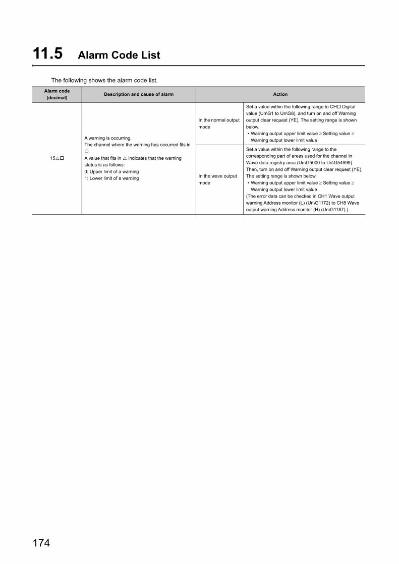
11.5 Alarm Code List
The following shows the alarm code list.
Alarm code
(decimal)Description and cause of alarm Action
15
A warning is occurring.
The channel where the warning has occurred fits in
.
A value that fits in indicates that the warning
status is as follows:
0: Upper limit of a warning
1: Lower limit of a warning
In the normal output
mode
Set a value within the following range to CH Digital
value (Un\G1 to Un\G8), and turn on and off Warning
output clear request (YE). The setting range is shown
below.
• Warning output upper limit value Setting value
Warning output lower limit value
In the wave output
mode
Set a value within the following range to the
corresponding part of areas used for the channel in
Wave data registry area (Un\G5000 to Un\G54999).
Then, turn on and off Warning output clear request (YE).
The setting range is shown below.
• Warning output upper limit value Setting value
Warning output lower limit value
(The error data can be checked in CH1 Wave output
warning Address monitor (L) (Un\G1172) to CH8 Wave
output warning Address monitor (H) (Un\G1187).)
174
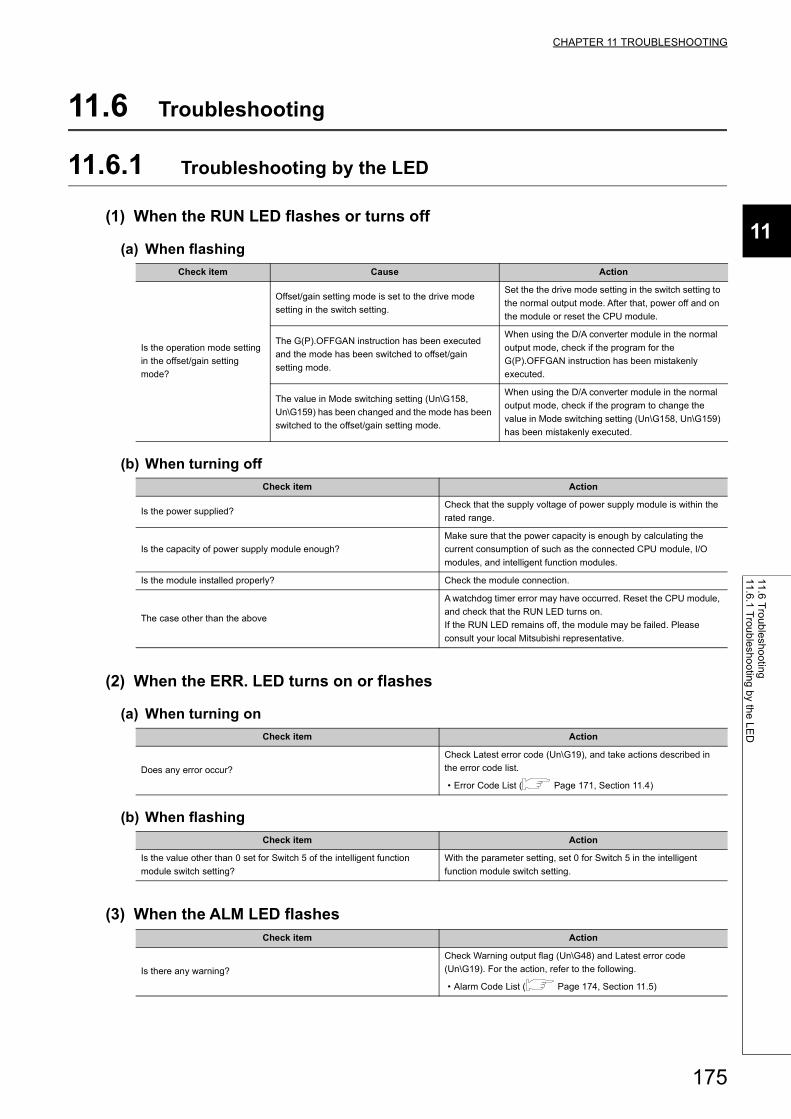
CHAPTER 11 TROUBLESHOOTING
11
11
.6 T
rou
ble
sho
otin
g1
1.6
.1 T
rou
ble
sho
otin
g b
y the
LE
D
11.6 Troubleshooting
11.6.1 Troubleshooting by the LED
(1) When the RUN LED flashes or turns off
(a) When flashing
(b) When turning off
(2) When the ERR. LED turns on or flashes
(a) When turning on
(b) When flashing
(3) When the ALM LED flashes
Check item Cause Action
Is the operation mode setting
in the offset/gain setting
mode?
Offset/gain setting mode is set to the drive mode
setting in the switch setting.
Set the the drive mode setting in the switch setting to
the normal output mode. After that, power off and on
the module or reset the CPU module.
The G(P).OFFGAN instruction has been executed
and the mode has been switched to offset/gain
setting mode.
When using the D/A converter module in the normal
output mode, check if the program for the
G(P).OFFGAN instruction has been mistakenly
executed.
The value in Mode switching setting (Un\G158,
Un\G159) has been changed and the mode has been
switched to the offset/gain setting mode.
When using the D/A converter module in the normal
output mode, check if the program to change the
value in Mode switching setting (Un\G158, Un\G159)
has been mistakenly executed.
Check item Action
Is the power supplied?Check that the supply voltage of power supply module is within the
rated range.
Is the capacity of power supply module enough?
Make sure that the power capacity is enough by calculating the
current consumption of such as the connected CPU module, I/O
modules, and intelligent function modules.
Is the module installed properly? Check the module connection.
The case other than the above
A watchdog timer error may have occurred. Reset the CPU module,
and check that the RUN LED turns on.
If the RUN LED remains off, the module may be failed. Please
consult your local Mitsubishi representative.
Check item Action
Does any error occur?
Check Latest error code (Un\G19), and take actions described in
the error code list.
• Error Code List ( Page 171, Section 11.4)
Check item Action
Is the value other than 0 set for Switch 5 of the intelligent function
module switch setting?
With the parameter setting, set 0 for Switch 5 in the intelligent
function module switch setting.
Check item Action
Is there any warning?
Check Warning output flag (Un\G48) and Latest error code
(Un\G19). For the action, refer to the following.
• Alarm Code List ( Page 174, Section 11.5)
175
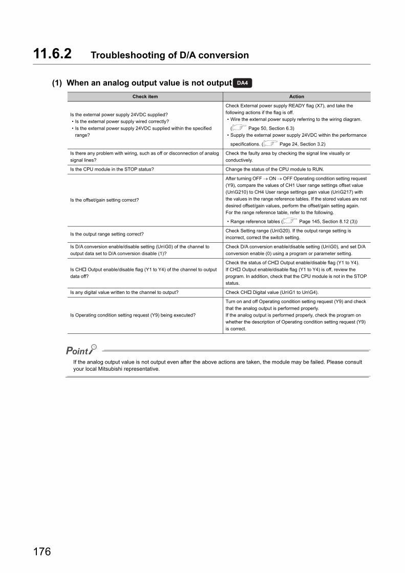
11.6.2 Troubleshooting of D/A conversion
(1) When an analog output value is not output
If the analog output value is not output even after the above actions are taken, the module may be failed. Please consult your local Mitsubishi representative.
Check item Action
Is the external power supply 24VDC supplied?
• Is the external power supply wired correctly?
• Is the external power supply 24VDC supplied within the specified
range?
Check External power supply READY flag (X7), and take the
following actions if the flag is off.
• Wire the external power supply referring to the wiring diagram.
( Page 50, Section 6.3)
• Supply the external power supply 24VDC within the performance
specifications. ( Page 24, Section 3.2)
Is there any problem with wiring, such as off or disconnection of analog
signal lines?
Check the faulty area by checking the signal line visually or
conductively.
Is the CPU module in the STOP status? Change the status of the CPU module to RUN.
Is the offset/gain setting correct?
After turning OFF ON OFF Operating condition setting request
(Y9), compare the values of CH1 User range settings offset value
(Un\G210) to CH4 User range settings gain value (Un\G217) with
the values in the range reference tables. If the stored values are not
desired offset/gain values, perform the offset/gain setting again.
For the range reference table, refer to the following.
• Range reference tables ( Page 145, Section 8.12 (3))
Is the output range setting correct?Check Setting range (Un\G20). If the output range setting is
incorrect, correct the switch setting.
Is D/A conversion enable/disable setting (Un\G0) of the channel to
output data set to D/A conversion disable (1)?
Check D/A conversion enable/disable setting (Un\G0), and set D/A
conversion enable (0) using a program or parameter setting.
Is CH Output enable/disable flag (Y1 to Y4) of the channel to output
data off?
Check the status of CH Output enable/disable flag (Y1 to Y4).
If CH Output enable/disable flag (Y1 to Y4) is off, review the
program. In addition, check that the CPU module is not in the STOP
status.
Is any digital value written to the channel to output? Check CH Digital value (Un\G1 to Un\G4).
Is Operating condition setting request (Y9) being executed?
Turn on and off Operating condition setting request (Y9) and check
that the analog output is performed properly.
If the analog output is performed properly, check the program on
whether the description of Operating condition setting request (Y9)
is correct.
DA4
176
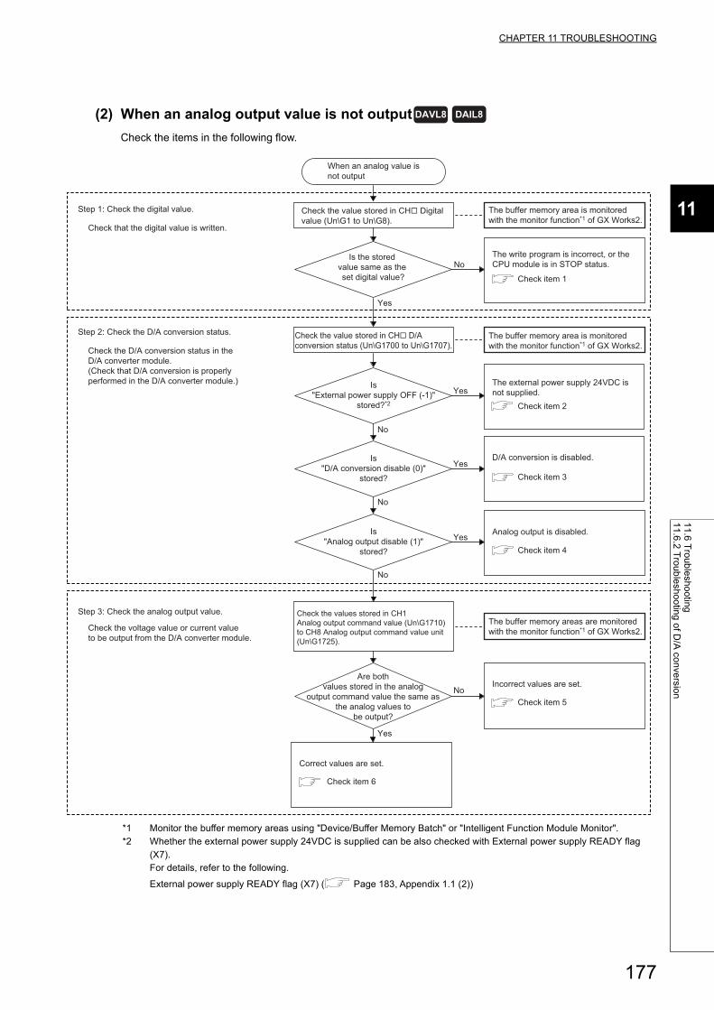
CHAPTER 11 TROUBLESHOOTING
11
11
.6 T
rou
ble
sho
otin
g1
1.6
.2 T
rou
ble
sho
otin
g o
f D/A
con
versio
n
(2) When an analog output value is not output
Check the items in the following flow.
*1 Monitor the buffer memory areas using "Device/Buffer Memory Batch" or "Intelligent Function Module Monitor".*2 Whether the external power supply 24VDC is supplied can be also checked with External power supply READY flag
(X7).For details, refer to the following.
External power supply READY flag (X7) ( Page 183, Appendix 1.1 (2))
DAVL8 DAIL8
No
Yes
No
No
Yes
Yes
No
No
Yes
Yes
When an analog value isnot output
Step 2: Check the D/A conversion status.
Is"D/A conversion disable (0)"
stored?
Check the value stored in CH� D/A conversion status (Un\G1700 to Un\G1707).
Check the values stored in CH1 Analog output command value (Un\G1710) to CH8 Analog output command value unit (Un\G1725).
Step 3: Check the analog output value.
Check the D/A conversion status in the D/A converter module. (Check that D/A conversion is properly performed in the D/A converter module.)
Check the voltage value or current value to be output from the D/A converter module.
Is"External power supply OFF (-1)"
stored?*2
Is"Analog output disable (1)"
stored?
Check the value stored in CH� Digital value (Un\G1 to Un\G8).
Is the stored value same as the set digital value?
The buffer memory area is monitoredwith the monitor function*1 of GX Works2.
Step 1: Check the digital value.
Check that the digital value is written.
The write program is incorrect, or theCPU module is in STOP status.
The buffer memory area is monitoredwith the monitor function*1 of GX Works2.
The external power supply 24VDC isnot supplied.
Are bothvalues stored in the analog
output command value the same asthe analog values to
be output?
The buffer memory areas are monitoredwith the monitor function*1 of GX Works2.
Incorrect values are set.
D/A conversion is disabled.
Analog output is disabled.
Correct values are set.
Check item 1
Check item 2
Check item 3
Check item 4
Check item 5
Check item 6
177
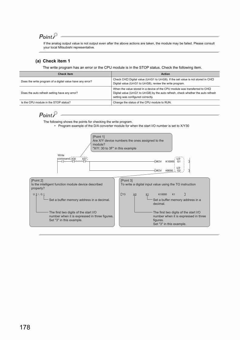
If the analog output value is not output even after the above actions are taken, the module may be failed. Please consult your local Mitsubishi representative.
(a) Check item 1
The write program has an error or the CPU module is in the STOP status. Check the following item.
The following shows the points for checking the write program.• Program example of the D/A converter module for when the start I/O number is set to X/Y30
Check item Action
Does the write program of a digital value have any error?Check CH Digital value (Un\G1 to Un\G8). If the set value is not stored in CH
Digital value (Un\G1 to Un\G8), review the write program.
Does the auto refresh setting have any error?
When the value stored in a device of the CPU module was transferred to CH
Digital value (Un\G1 to Un\G8) by the auto refresh, check whether the auto refresh
setting was configured correctly.
Is the CPU module in the STOP status? Change the status of the CPU module to RUN.
[Point 1]Are X/Y device numbers the ones assigned to themodule? "X/Y: 30 to 3F" in this example
[Point 3]To write a digital input value using the TO instruction
Set a buffer memory address in adecimal.
The first two digits of the start I/Onumber when it is expressed in threefigures.Set "3" in this example.
[Point 2]Is the intelligent function module device describedproperly?
Set a buffer memory address in a decimal.
The first two digits of the start I/Onumber when it is expressed in three figures.Set "3" in this example.
\
Write command
178
CHAPTER 11 TROUBLESHOOTING
11
11
.6 T
rou
ble
sho
otin
g1
1.6
.2 T
rou
ble
sho
otin
g o
f D/A
con
versio
n
(b) Check item 2
The external power supply 24VDC is not supplied. Check the following item.
(c) Check item 3
D/A conversion is not enabled. Check the following item.
(d) Check item 4
Analog output is not enabled. Check the following item.
(e) Check item 5
The setting value is incorrect. Check the following item.
(f) Check item 6
A correct value is set for each setting. Check the following item.
Check item Action
Is the external power supply 24VDC supplied?
• Is the external power supply wired correctly?
• Is the external power supply 24VDC supplied within the specified
range?
• Wire the external power supply referring to the wiring diagram. ( Page 50,
Section 6.3)
• Supply the external power supply 24VDC within the performance specifications.
( Page 24, Section 3.2)
Check item Action
Is D/A conversion enable/disable setting (Un\G0) of the channel to
output data set to D/A conversion disable (1)?
Check D/A conversion enable/disable setting (Un\G0), and set D/A conversion
enable (0) using a program or parameter setting.
Has Operating condition setting request (Y9) been executed?
Check that the analog output is performed properly after turning on and off Operating
condition setting request (Y9).
If the analog output is performed properly, check the program on whether the
description of Operating condition setting request (Y9) is correct.
Check item Action
Is CH Output enable/disable flag (Y1 to Y8) of the channel to output
data off?
Check the status of CH Output enable/disable flag (Y1 to Y8).
If CH Output enable/disable flag (Y1 to Y8) is off, review the program. In addition,
check that the CPU module is not in the STOP status.
Check item Action
Is the output range setting correct?Check Setting range (Un\G20, Un\G21). If the output range setting is incorrect,
correct the switch setting.
Is the offset/gain setting correct?
After turning on and off Operating condition setting request (Y9), compare the values
of CH1 User range settings offset value (Un\G218) to CH8 User range settings gain
value (Un\G233) with the values in the range reference tables. If the stored values
are not desired offset/gain values, perform the offset/gain setting again.
For the range reference table, refer to the following.
• Range reference tables ( Page 145, Section 8.12 (3))
Check item Action
Is there any problem with wiring, such as off or disconnection of analog
signal lines?Check the faulty area by checking the signal line visually or conductively.
179
(3) When HOLD of analog output value is not available
(4) When analog value is not output in the wave output modeCheck the items in the following procedure.
For details on the wave output function, refer to the following.
• Wave Output Function ( Page 86, Section 8.8)
Check item Action
Is the analog output HOLD/CLEAR function setting correct?
Check HOLD/CLEAR function setting (Un\G26, Un\G27). If the
HOLD/CLEAR function setting is incorrect, correct the switch
setting.
Is the D/A converter module used with the head module?
Refer to the points in the following section and check that the setting
is made for using the analog output HOLD/CLEAR function with the
head module.
• Analog Output HOLD/CLEAR Function ( Page 71, Section
8.4)
No. Check item Action
1 Check the switch setting.
Is the drive mode setting correct?
Check that Offset/gain setting mode flag (XA) is off. Then, check
Normal (D/A Converter Processing) Mode is set for the drive mode
setting.
If Normal (D/A Converter Processing) Mode is not set, set Drive Mode
Setting to Normal (D/A Converter Processing) Mode.
Is the output mode setting correct?
Check that Wave output mode is set for Output mode (Un\G9).
If the wave output mode is not set, set "Output mode setting" in "Switch
Setting" to "Wave output mode".
Is the user range setting selected?
When Wave output mode is used, the user range setting cannot be
selected for the output range.
If the user range setting is set to the output range, set the value other
than the user range setting.
2 Checking the program
Is D/A conversion enable/disable setting
(Un\G0) of the channel to output wave
data set to D/A conversion disable (1)?
Check D/A conversion enable/disable setting (Un\G0) and set D/A
conversion enable (0).
Is Operating condition setting request
(Y9) being executed?
Turn OFF ON OFF Operating condition setting request (Y9) to
enable the parameter setting of the wave output function.
Is any value written to Wave data
registry area (Un\G5000 to Un\G54999)
which is used for the channel to output
wave data?
Check the value in Wave data registry area (Un\G5000 to Un\G54999)
which is used for the channel to output wave data.
During a pause of the wave output, the monitors of the wave output
function can be checked. After setting the analog output HOLD/CLEAR
function to HOLD, set CH Wave output start/stop request (Un\G1000
to Un\G1007) to Wave output pause request (2) to pause the wave
output. Then, check the monitors.
Is CH Wave output start/stop request
(Un\G1000 to Un\G1007) of the channel
to output wave data set to Wave output
stop request (0)?
Check CH Wave output status monitor (Un\G1100 to Un\G1107) of
the channel to output wave data.
If CH Wave output status monitor (Un\G1100 to Un\G1107) is set to
Wave output stop (0), set CH Wave output start/stop request
(Un\G1000 to Un\G1007) to Wave output start request (1).
Is CH Output enable/disable flag (Y1
to Y8) of the channel to output wave
data on?
Check the status of CH Output enable/disable flag (Y1 to Y8). If CH
Output enable/disable flag (Y1 to Y8) is off, review the program.
3Checking the connection
method
Is the external power supply 24VDC
supplied?
Check External power supply READY flag (X7), and if the flag is off,
supply a 24VDC to the external power supply terminal. The following
shows the pin numbers of the external power supply terminal.
• Pin number for the L60DA4: 16, 17
• Pin number for the L60DAVL8, L60DAIL8: 17, 18
180
CHAPTER 11 TROUBLESHOOTING
11
11
.6 T
rou
ble
sho
otin
g1
1.6
.2 T
rou
ble
sho
otin
g o
f D/A
con
versio
n
(5) When External power supply READY flag (X7) does not turn onCheck item Action
Is the external power supply 24VDC supplied?
(1) Is the external power supply correctly wired?
(2) Is the external power supply 24VDC supplied within the specified
range?
(1) Wire the external power supply by referring to the external
wiring example. ( Page 52, Section 6.4)
(2) Supply 24VDC within the range of the performance
specifications. ( Page 24, Section 3.2)
The case other than the aboveThe possible cause is a failure of the D/A converter module. Please
consult your local Mitsubishi representative.
181
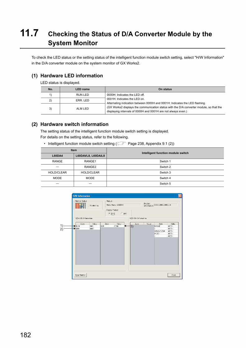
11.7 Checking the Status of D/A Converter Module by the System Monitor
To check the LED status or the setting status of the intelligent function module switch setting, select "H/W Information"
in the D/A converter module on the system monitor of GX Works2.
(1) Hardware LED informationLED status is displayed.
(2) Hardware switch informationThe setting status of the intelligent function module switch setting is displayed.
For details on the setting status, refer to the following.
• Intelligent function module switch setting ( Page 238, Appendix 9.1 (2))
No. LED name On status
1) RUN LED 0000H: Indicates the LED off.
0001H: Indicates the LED on.
Alternating indication between 0000H and 0001H: Indicates the LED flashing.
(GX Works2 displays the communication status with the D/A converter module, so that the
displaying intervals of 0000H and 0001H are not always even.)
2) ERR. LED
3) ALM LED
ItemIntelligent function module switch
L60DA4 L60DAVL8, L60DAIL8
RANGE RANGE1 Switch 1
RANGE2 Switch 2
HOLD/CLEAR HOLD/CLEAR Switch 3
MODE MODE Switch 4
Switch 5
1)2)
3)
182
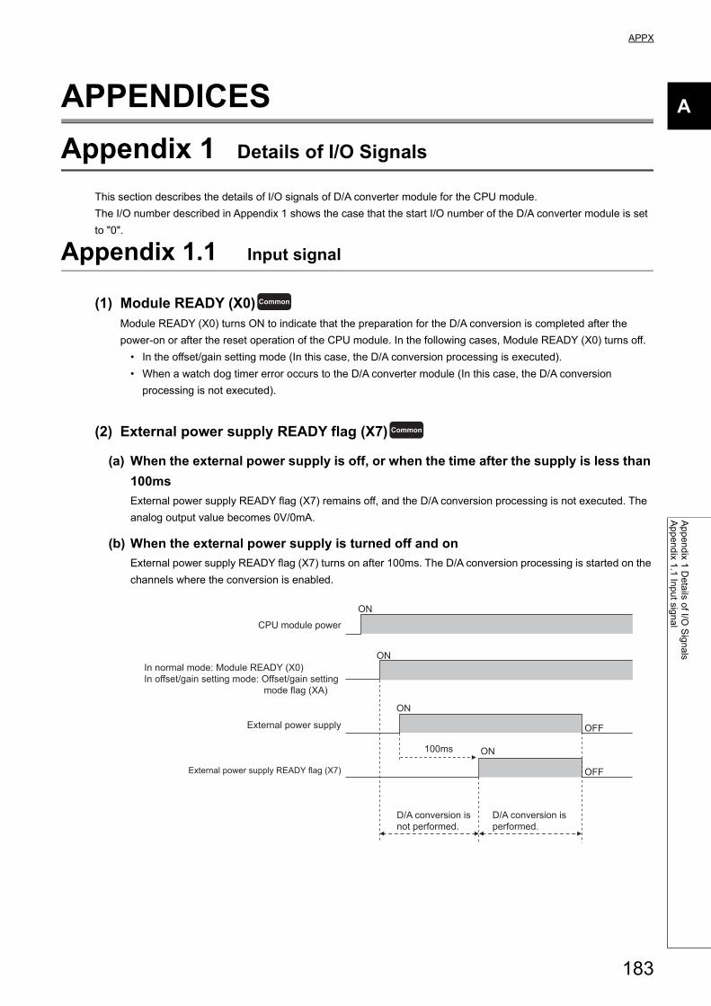
APPX
A
Ap
pe
nd
ix 1 D
eta
ils of I/O
Sig
na
lsA
pp
en
dix 1
.1 In
pu
t sign
al
APPENDICES
Appendix 1 Details of I/O Signals
This section describes the details of I/O signals of D/A converter module for the CPU module.
The I/O number described in Appendix 1 shows the case that the start I/O number of the D/A converter module is set
to "0".
Appendix 1.1 Input signal
(1) Module READY (X0)Module READY (X0) turns ON to indicate that the preparation for the D/A conversion is completed after the
power-on or after the reset operation of the CPU module. In the following cases, Module READY (X0) turns off.
• In the offset/gain setting mode (In this case, the D/A conversion processing is executed).
• When a watch dog timer error occurs to the D/A converter module (In this case, the D/A conversion
processing is not executed).
(2) External power supply READY flag (X7)
(a) When the external power supply is off, or when the time after the supply is less than
100ms
External power supply READY flag (X7) remains off, and the D/A conversion processing is not executed. The
analog output value becomes 0V/0mA.
(b) When the external power supply is turned off and on
External power supply READY flag (X7) turns on after 100ms. The D/A conversion processing is started on the
channels where the conversion is enabled.
Common
Common
External power supply
D/A conversion is
not performed.
CPU module power
In normal mode: Module READY (X0)
In offset/gain setting mode: Offset/gain setting
mode flag (XA)
External power supply READY flag (X7)
ON
ON
ON
OFF
OFF
100ms ON
D/A conversion is
performed.
183
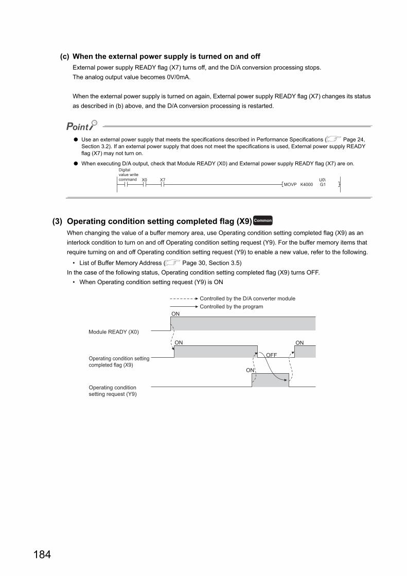
(c) When the external power supply is turned on and off
External power supply READY flag (X7) turns off, and the D/A conversion processing stops.
The analog output value becomes 0V/0mA.
When the external power supply is turned on again, External power supply READY flag (X7) changes its status
as described in (b) above, and the D/A conversion processing is restarted.
● Use an external power supply that meets the specifications described in Performance Specifications ( Page 24, Section 3.2). If an external power supply that does not meet the specifications is used, External power supply READY flag (X7) may not turn on.
● When executing D/A output, check that Module READY (X0) and External power supply READY flag (X7) are on.
(3) Operating condition setting completed flag (X9)When changing the value of a buffer memory area, use Operating condition setting completed flag (X9) as an
interlock condition to turn on and off Operating condition setting request (Y9). For the buffer memory items that
require turning on and off Operating condition setting request (Y9) to enable a new value, refer to the following.
• List of Buffer Memory Address ( Page 30, Section 3.5)
In the case of the following status, Operating condition setting completed flag (X9) turns OFF.
• When Operating condition setting request (Y9) is ON
Digital value write command
Common
Module READY (X0)
Operating condition setting
completed flag (X9)
Operating condition
setting request (Y9)
Controlled by the D/A converter module
Controlled by the program
ON
ON
ON
ON
OFF
184
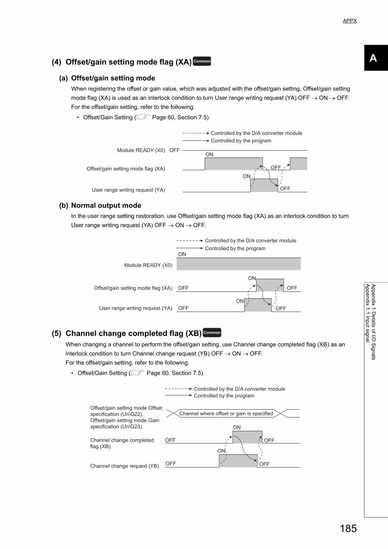
APPX
A
Ap
pe
nd
ix 1 D
eta
ils of I/O
Sig
na
lsA
pp
en
dix 1
.1 In
pu
t sign
al
(4) Offset/gain setting mode flag (XA)
(a) Offset/gain setting mode
When registering the offset or gain value, which was adjusted with the offset/gain setting, Offset/gain setting
mode flag (XA) is used as an interlock condition to turn User range writing request (YA) OFF ON OFF.
For the offset/gain setting, refer to the following.
• Offset/Gain Setting ( Page 60, Section 7.5)
(b) Normal output mode
In the user range setting restoration, use Offset/gain setting mode flag (XA) as an interlock condition to turn
User range writing request (YA) OFF ON OFF.
(5) Channel change completed flag (XB)When changing a channel to perform the offset/gain setting, use Channel change completed flag (XB) as an
interlock condition to turn Channel change request (YB) OFF ON OFF.
For the offset/gain setting, refer to the following.
• Offset/Gain Setting ( Page 60, Section 7.5)
Common
OFFModule READY (X0)
Offset/gain setting mode flag (XA)
User range writing request (YA)
Controlled by the D/A converter moduleControlled by the program
ON
OFF
OFF
ON
ON
Module READY (X0)
Offset/gain setting mode flag (XA)
User range writing request (YA)
ON
ON
OFF
OFF
OFF
OFF
Controlled by the D/A converter moduleControlled by the program
Common
Offset/gain setting mode Offset
specification (Un\G22),
Offset/gain setting mode Gain
specification (Un\G23)
Channel change completed
flag (XB)
Channel change request (YB)
OFF
OFF
ON
ON
OFF
OFF
Controlled by the D/A converter module
Controlled by the program
Channel where offset or gain is specified
185
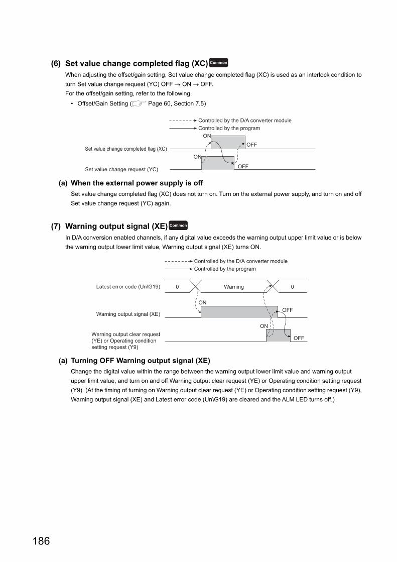
(6) Set value change completed flag (XC)When adjusting the offset/gain setting, Set value change completed flag (XC) is used as an interlock condition to
turn Set value change request (YC) OFF ON OFF.
For the offset/gain setting, refer to the following.
• Offset/Gain Setting ( Page 60, Section 7.5)
(a) When the external power supply is off
Set value change completed flag (XC) does not turn on. Turn on the external power supply, and turn on and off
Set value change request (YC) again.
(7) Warning output signal (XE)In D/A conversion enabled channels, if any digital value exceeds the warning output upper limit value or is below
the warning output lower limit value, Warning output signal (XE) turns ON.
(a) Turning OFF Warning output signal (XE)
Change the digital value within the range between the warning output lower limit value and warning output
upper limit value, and turn on and off Warning output clear request (YE) or Operating condition setting request
(Y9). (At the timing of turning on Warning output clear request (YE) or Operating condition setting request (Y9),
Warning output signal (XE) and Latest error code (Un\G19) are cleared and the ALM LED turns off.)
Common
Set value change request (YC)
Set value change completed flag (XC)
Controlled by the D/A converter module
Controlled by the program
ON
OFF
ON
OFF
Common
Warning output signal (XE)
Latest error code (Un\G19)
Warning output clear request(YE) or Operating condition setting request (Y9)
Controlled by the D/A converter moduleControlled by the program
ON
ON
OFF
OFF
0 0Warning
186
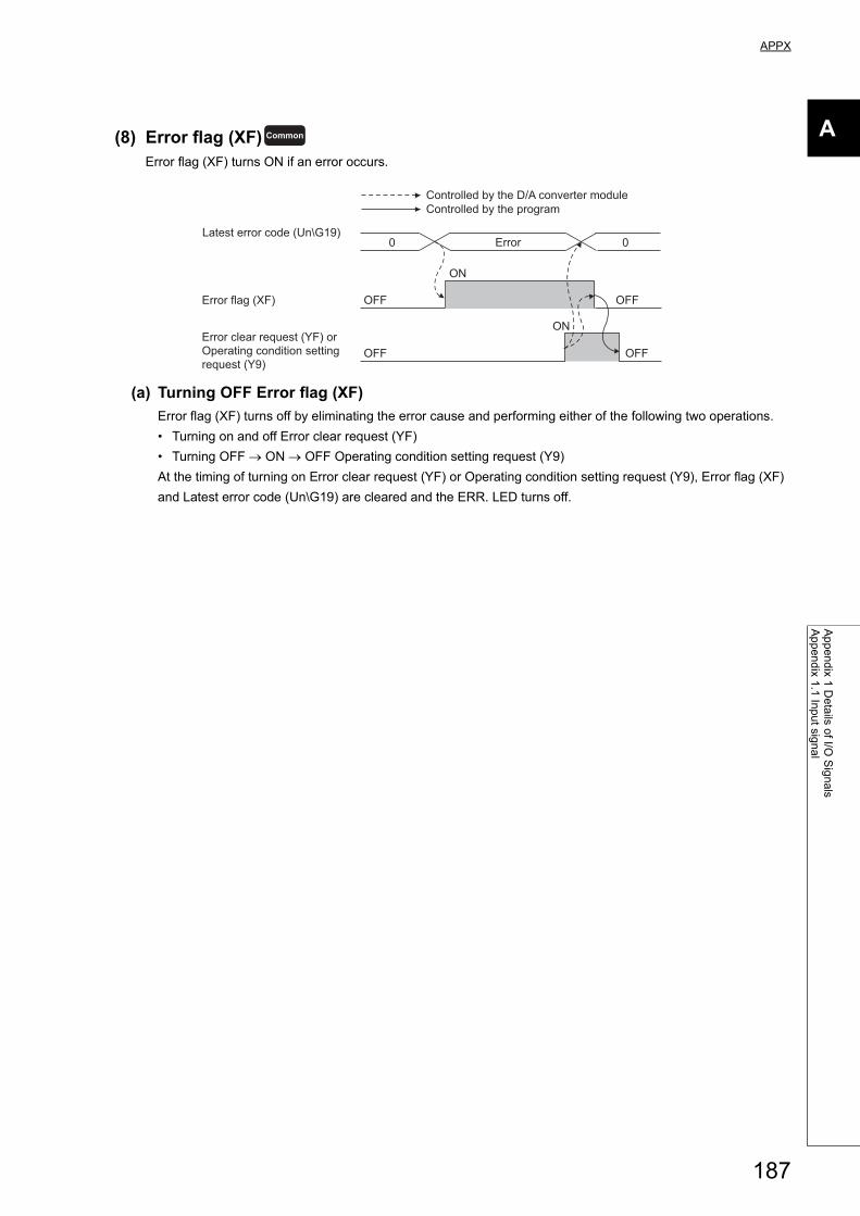
APPX
A
Ap
pe
nd
ix 1 D
eta
ils of I/O
Sig
na
lsA
pp
en
dix 1
.1 In
pu
t sign
al
(8) Error flag (XF)Error flag (XF) turns ON if an error occurs.
(a) Turning OFF Error flag (XF)
Error flag (XF) turns off by eliminating the error cause and performing either of the following two operations.
• Turning on and off Error clear request (YF)
• Turning OFF ON OFF Operating condition setting request (Y9)
At the timing of turning on Error clear request (YF) or Operating condition setting request (Y9), Error flag (XF)
and Latest error code (Un\G19) are cleared and the ERR. LED turns off.
Common
ErrorLatest error code (Un\G19)
Error flag (XF)
Error clear request (YF) or
Operating condition setting
request (Y9)
OFF
OFF
OFF
OFF
ON
0 0
ON
Controlled by the D/A converter module
Controlled by the program
187
Appendix 1.2 Output signal
(1) CH Output enable/disable flag (Y1 to Y8)This function sets whether to output the D/A-converted value or the offset value, for each channel.
ON : D/A conversion value
OFF : offset value
(a) D/A conversion speed
The D/A conversion speed is calculated by a conversion speed (the number of conversion enabled channels)
regardless of turning on CH Output enable/disable flag (Y1 to Y8). The conversion speed differs depending
on the module used.
(2) Operating condition setting request (Y9)To enable the initial setting of the D/A converter module, turn Operating condition setting request (Y9) OFF ON
OFF.
For the contents of the initial setting which becomes enabled and the timing of turning the signal OFF ON
OFF, refer to the following.
• Operating condition setting completed flag (X9) ( Page 184, Appendix 1.1 (3))
By eliminating the error cause and turning OFF ON OFF this signal while an error or a warning is occurring,
the error and the warning is cleared.
In the wave output mode, check that CH Wave output status monitor (Un\G1100 to Un\G1107) in all channels
are set to Wave output stop (0) and turn on and off Operating condition setting request (Y9). When Operating
condition setting request (Y9) is turned on and off with a channel set to other than the Wave output stop, an error
occurs. The error code (20) is stored in Latest error code (Un\G19), Error flag (XF) turns on, and the ERR.LED
turns on. The initial setting cannot be enabled.
(3) User range writing request (YA)
(a) Offset/gain setting mode
Turn User range writing request (YA) OFF ON OFF to register the adjusted offset/gain setting values in
the D/A converter module.
At the timing of turning on this signal, data is written to the flash memory.
For the timing of turning the signal OFF ON OFF, refer to the following.
• Offset/gain setting mode flag (XA) ( Page 185, Appendix 1.1 (4))
For the offset/gain setting, refer to the following.
• Offset/Gain Setting ( Page 60, Section 7.5)
Module Conversion speed
L60DA4 20s/CH
L60DAVL8, L60DAIL8 200s/CH
Common
Common
Common
188
APPX
A
Ap
pe
nd
ix 1 D
eta
ils of I/O
Sig
na
lsA
pp
en
dix 1
.2 O
utp
ut sig
na
l
(b) Normal output mode
Turn on and off User range writing request (YA) to restore the user range setting.
For the timing of turning the signal OFF ON OFF, refer to the following.
• Offset/gain setting mode flag (XA) ( Page 185, Appendix 1.1 (4))
For user range restoration, refer to the following.
• Save/Restoration of Offset/Gain Value ( Page 140, Section 8.12)
(c) Wave output mode
Even though User range writing request (YA) is turned OFF ON OFF in the wave output mode, the user
range cannot be restored. When restoring the user range, set the normal output mode.
(4) Channel change request (YB)Turn Channel change request (YB) OFF ON OFF to change a channel to perform the offset/gain setting.
For the timing of turning the signal OFF ON OFF, refer to the following.
• Channel change completed flag (XB) ( Page 185, Appendix 1.1 (5))
For the offset/gain setting, refer to the following.
• Offset/Gain Setting ( Page 60, Section 7.5)
(5) Set value change request (YC)Turn Set value change request (YC) OFF ON OFF to change the analog output value during the adjustment
of offset/gain setting.
The analog output value is changed according to the value set in Offset/gain adjustment value specification
(Un\G24).
For the timing of turning the signal OFF ON OFF, refer to the following.
• Set value change completed flag (XC) ( Page 186, Appendix 1.1 (6))
For the offset/gain setting, refer to the following.
• Offset/Gain Setting ( Page 60, Section 7.5)
(6) Warning output clear request (YE)Turn Warning output clear request (YE) OFF ON OFF to clear the warning output.
For the timing of turning the signal OFF ON OFF, refer to the following.
• Warning output signal (XE) ( Page 186, Appendix 1.1 (7))
(7) Error clear request (YF)To clear Error flag (XF) and Latest error code (Un\G19), turn on and off Error clear request (YF).
For the timing of turning the signal OFF ON OFF, refer to the following.
• Error flag (XF) ( Page 187, Appendix 1.1 (8))
Common
Common
Common
Common
189
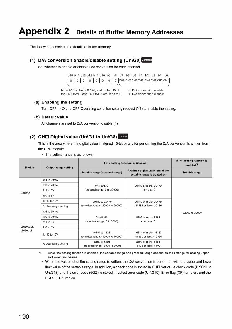
Appendix 2 Details of Buffer Memory Addresses
The following describes the details of buffer memory.
(1) D/A conversion enable/disable setting (Un\G0)Set whether to enable or disable D/A conversion for each channel.
(a) Enabling the setting
Turn OFF ON OFF Operating condition setting request (Y9) to enable the setting.
(b) Default value
All channels are set to D/A conversion disable (1).
(2) CH Digital value (Un\G1 to Un\G8)This is the area where the digital value in signed 16-bit binary for performing the D/A conversion is written from
the CPU module.
• The setting range is as follows;
*1 When the scaling function is enabled, the settable range and practical range depend on the settings for scaling upper and lower limit values.
• When the value out of the setting range is written, the D/A conversion is performed with the upper and lower
limit value of the settable range. In addition, a check code is stored in CH Set value check code (Un\G11 to
Un\G18) and the error code (60) is stored in Latest error code (Un\G19), Error flag (XF) turns on, and the
ERR. LED turns on.
Module Output range setting
If the scaling function is disabledIf the scaling function is
enabled*1
Settable range (practical range)A written digital value out of the
settable range is treated asSettable range
L60DA4
0: 4 to 20mA
0 to 20479
(practical range: 0 to 20000)
20480 or more: 20479
-1 or less: 0
-32000 to 32000
1: 0 to 20mA
2: 1 to 5V
3: 0 to 5V
4: -10 to 10V -20480 to 20479
(practical range: -20000 to 20000)
20480 or more: 20479
-20481 or less: -20480F: User range setting
L60DAVL8,
L60DAIL8
0: 4 to 20mA
0 to 8191
(practical range: 0 to 8000)
8192 or more: 8191
-1 or less: 0
1: 0 to 20mA
2: 1 to 5V
3: 0 to 5V
4: -10 to 10V-16384 to 16383
(practical range: -16000 to 16000)
16384 or more: 16383
-16385 or less: -16384
F: User range setting-8192 to 8191
(practical range: -8000 to 8000)
8192 or more: 8191
-8193 or less: -8192
Common
0 0 0 0 0 0 0 0 CH1CH2CH3CH4CH5CH6CH7CH8
b15 b14 b13 b12 b11 b10 b9 b8 b7 b6 b5 b0b1b2b3b4
0: D/A conversion enable1: D/A conversion disable
b4 to b15 of the L60DA4, and b8 to b15 of the L60DAVL8 and L60DAIL8 are fixed to 0.
Common
190
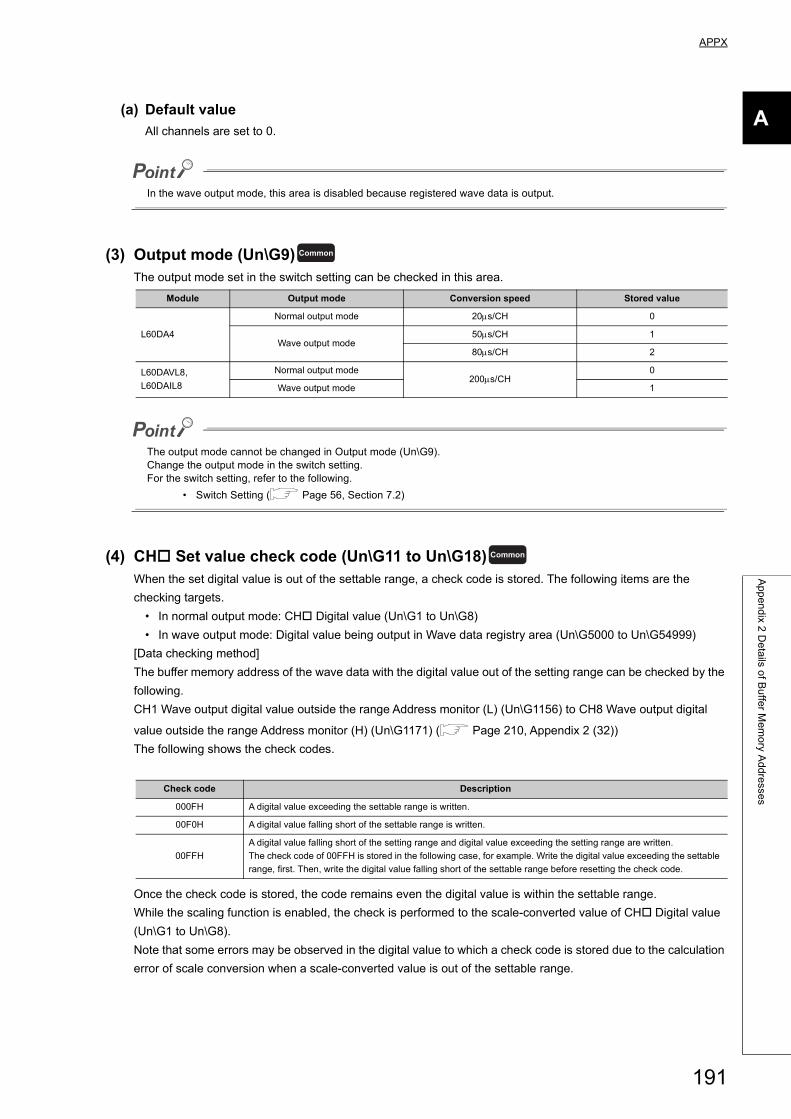
APPX
A
Ap
pe
nd
ix 2 D
eta
ils of B
uffe
r Me
mo
ry Ad
dre
sses
(a) Default value
All channels are set to 0.
In the wave output mode, this area is disabled because registered wave data is output.
(3) Output mode (Un\G9)The output mode set in the switch setting can be checked in this area.
The output mode cannot be changed in Output mode (Un\G9).Change the output mode in the switch setting.For the switch setting, refer to the following.
• Switch Setting ( Page 56, Section 7.2)
(4) CH Set value check code (Un\G11 to Un\G18)When the set digital value is out of the settable range, a check code is stored. The following items are the
checking targets.
• In normal output mode: CH Digital value (Un\G1 to Un\G8)
• In wave output mode: Digital value being output in Wave data registry area (Un\G5000 to Un\G54999)
[Data checking method]
The buffer memory address of the wave data with the digital value out of the setting range can be checked by the
following.
CH1 Wave output digital value outside the range Address monitor (L) (Un\G1156) to CH8 Wave output digital
value outside the range Address monitor (H) (Un\G1171) ( Page 210, Appendix 2 (32))
The following shows the check codes.
Once the check code is stored, the code remains even the digital value is within the settable range.
While the scaling function is enabled, the check is performed to the scale-converted value of CH Digital value
(Un\G1 to Un\G8).
Note that some errors may be observed in the digital value to which a check code is stored due to the calculation
error of scale conversion when a scale-converted value is out of the settable range.
Module Output mode Conversion speed Stored value
L60DA4
Normal output mode 20s/CH 0
Wave output mode50s/CH 1
80s/CH 2
L60DAVL8,
L60DAIL8
Normal output mode200s/CH
0
Wave output mode 1
Check code Description
000FH A digital value exceeding the settable range is written.
00F0H A digital value falling short of the settable range is written.
00FFH
A digital value falling short of the setting range and digital value exceeding the setting range are written.
The check code of 00FFH is stored in the following case, for example. Write the digital value exceeding the settable
range, first. Then, write the digital value falling short of the settable range before resetting the check code.
Common
Common
191
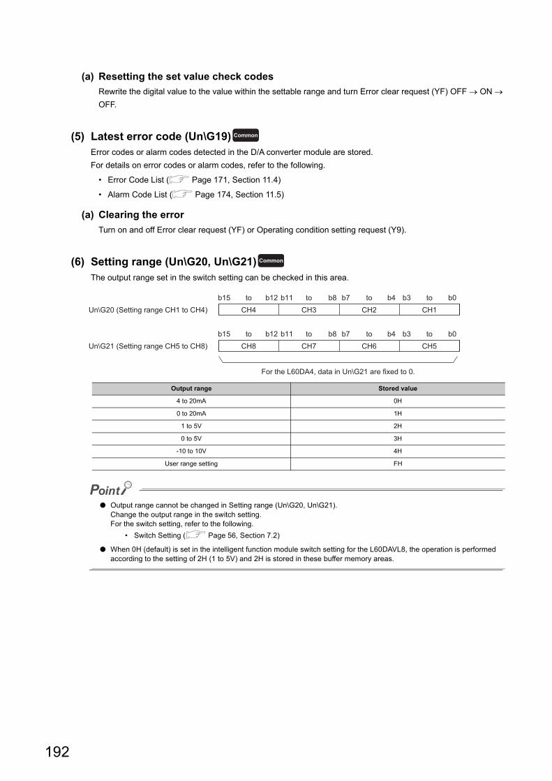
(a) Resetting the set value check codes
Rewrite the digital value to the value within the settable range and turn Error clear request (YF) OFF ON
OFF.
(5) Latest error code (Un\G19)Error codes or alarm codes detected in the D/A converter module are stored.
For details on error codes or alarm codes, refer to the following.
• Error Code List ( Page 171, Section 11.4)
• Alarm Code List ( Page 174, Section 11.5)
(a) Clearing the error
Turn on and off Error clear request (YF) or Operating condition setting request (Y9).
(6) Setting range (Un\G20, Un\G21)The output range set in the switch setting can be checked in this area.
● Output range cannot be changed in Setting range (Un\G20, Un\G21).Change the output range in the switch setting.For the switch setting, refer to the following.
• Switch Setting ( Page 56, Section 7.2)
● When 0H (default) is set in the intelligent function module switch setting for the L60DAVL8, the operation is performed according to the setting of 2H (1 to 5V) and 2H is stored in these buffer memory areas.
Output range Stored value
4 to 20mA 0H
0 to 20mA 1H
1 to 5V 2H
0 to 5V 3H
-10 to 10V 4H
User range setting FH
Common
Common
CH1CH2CH3CH4
CH5CH6CH7CH8
b15 to b12 b11 to b8 b7 to b0tob3b4
b15 to b12 b11 to b8 b7 to b0tob3b4
Un\G20 (Setting range CH1 to CH4)
Un\G21 (Setting range CH5 to CH8)
For the L60DA4, data in Un\G21 are fixed to 0.
192
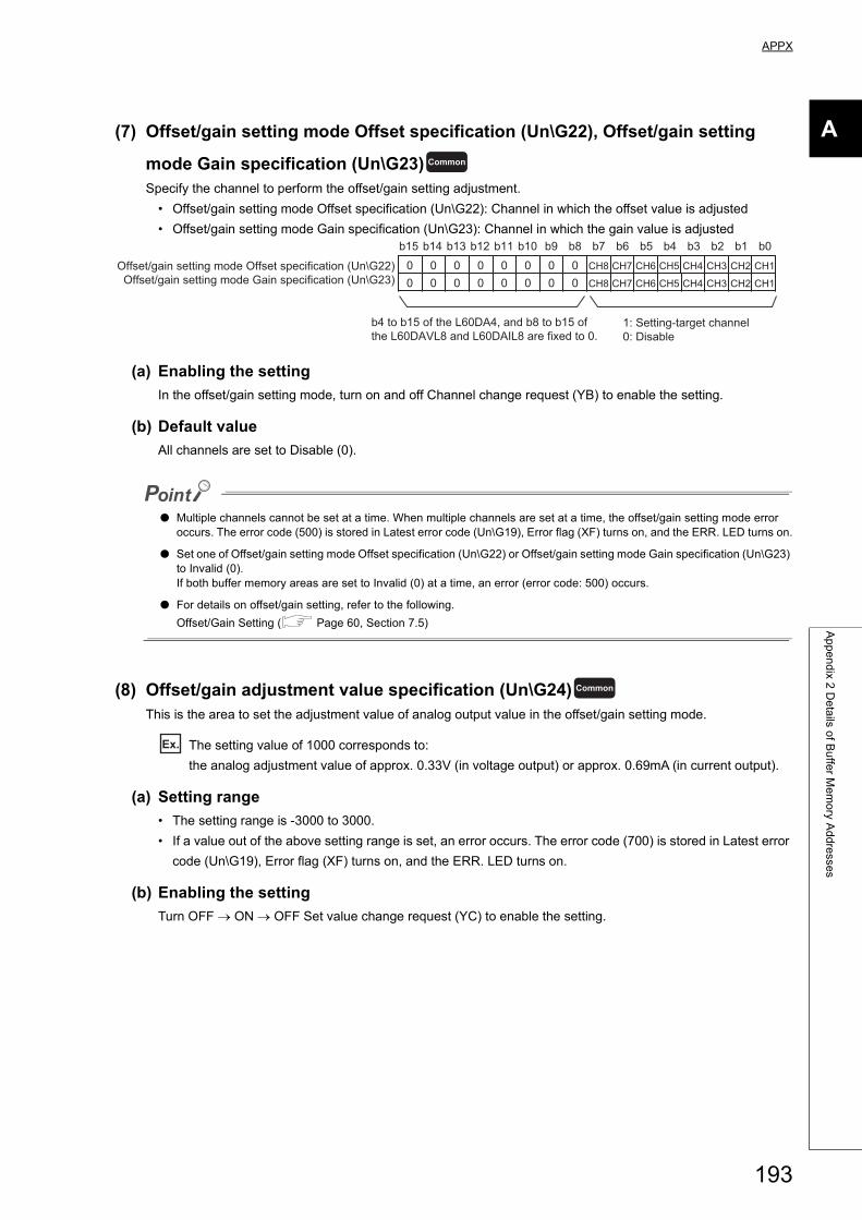
APPX
A
Ap
pe
nd
ix 2 D
eta
ils of B
uffe
r Me
mo
ry Ad
dre
sses
(7) Offset/gain setting mode Offset specification (Un\G22), Offset/gain setting
mode Gain specification (Un\G23)Specify the channel to perform the offset/gain setting adjustment.
• Offset/gain setting mode Offset specification (Un\G22): Channel in which the offset value is adjusted
• Offset/gain setting mode Gain specification (Un\G23): Channel in which the gain value is adjusted
(a) Enabling the setting
In the offset/gain setting mode, turn on and off Channel change request (YB) to enable the setting.
(b) Default value
All channels are set to Disable (0).
● Multiple channels cannot be set at a time. When multiple channels are set at a time, the offset/gain setting mode error occurs. The error code (500) is stored in Latest error code (Un\G19), Error flag (XF) turns on, and the ERR. LED turns on.
● Set one of Offset/gain setting mode Offset specification (Un\G22) or Offset/gain setting mode Gain specification (Un\G23) to Invalid (0).If both buffer memory areas are set to Invalid (0) at a time, an error (error code: 500) occurs.
● For details on offset/gain setting, refer to the following.
Offset/Gain Setting ( Page 60, Section 7.5)
(8) Offset/gain adjustment value specification (Un\G24)This is the area to set the adjustment value of analog output value in the offset/gain setting mode.
Ex. The setting value of 1000 corresponds to:
the analog adjustment value of approx. 0.33V (in voltage output) or approx. 0.69mA (in current output).
(a) Setting range
• The setting range is -3000 to 3000.
• If a value out of the above setting range is set, an error occurs. The error code (700) is stored in Latest error
code (Un\G19), Error flag (XF) turns on, and the ERR. LED turns on.
(b) Enabling the setting
Turn OFF ON OFF Set value change request (YC) to enable the setting.
Common
0 0 0 0 0 0 0 0 CH1CH2CH3CH4
0 0 0 0 0 0 0 0 CH1CH2CH3CH4
CH5CH6CH7CH8
CH5CH6CH7CH8
b15 b14 b13 b12 b11 b10 b9 b8 b7 b6 b5 b0b1b2b3b4
1: Setting-target channel0: Disable
b4 to b15 of the L60DA4, and b8 to b15 of the L60DAVL8 and L60DAIL8 are fixed to 0.
Offset/gain setting mode Offset specification (Un\G22)Offset/gain setting mode Gain specification (Un\G23)
Common
193
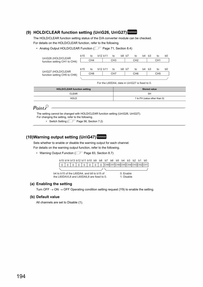
(9) HOLD/CLEAR function setting (Un\G26, Un\G27)The HOLD/CLEAR function setting status of the D/A converter module can be checked.
For details on the HOLD/CLEAR function, refer to the following.
• Analog Output HOLD/CLEAR Function ( Page 71, Section 8.4)
The setting cannot be changed with HOLD/CLEAR function setting (Un\G26, Un\G27).For changing the setting, refer to the following.
• Switch Setting ( Page 56, Section 7.2)
(10)Warning output setting (Un\G47)Sets whether to enable or disable the warning output for each channel.
For details on the warning output function, refer to the following.
• Warning Output Function ( Page 83, Section 8.7)
(a) Enabling the setting
Turn OFF ON OFF Operating condition setting request (Y9) to enable the setting.
(b) Default value
All channels are set to Disable (1).
HOLD/CLEAR function setting Stored value
CLEAR 0H
HOLD 1 to FH (value other than 0)
Common
CH1CH2CH3CH4
CH5CH6CH7CH8
b15 to b12 b11 to b8 b7 to b0tob3b4
b15 to b12 b11 to b8 b7 to b0tob3b4
Un\G26 (HOLD/CLEAR function setting CH1 to CH4)
Un\G27 (HOLD/CLEAR function setting CH5 to CH8)
For the L60DA4, data in Un\G27 is fixed to 0.
Common
0 0 0 0 0 0 0 0 CH1CH2CH3CH4CH5CH6CH7CH8
b15 b14 b13 b12 b11 b10 b9 b8 b7 b6 b5 b0b1b2b3b4
0: Enable1: Disable
b4 to b15 of the L60DA4, and b8 to b15 of the L60DAVL8 and L60DAIL8 are fixed to 0.
194
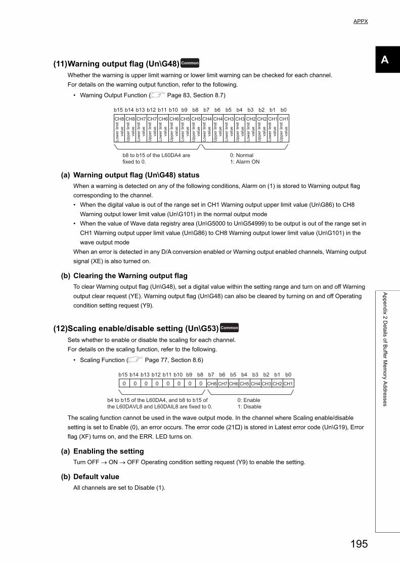
APPX
A
Ap
pe
nd
ix 2 D
eta
ils of B
uffe
r Me
mo
ry Ad
dre
sses
(11)Warning output flag (Un\G48)Whether the warning is upper limit warning or lower limit warning can be checked for each channel.
For details on the warning output function, refer to the following.
• Warning Output Function ( Page 83, Section 8.7)
(a) Warning output flag (Un\G48) status
When a warning is detected on any of the following conditions, Alarm on (1) is stored to Warning output flag
corresponding to the channel.
• When the digital value is out of the range set in CH1 Warning output upper limit value (Un\G86) to CH8
Warning output lower limit value (Un\G101) in the normal output mode
• When the value of Wave data registry area (Un\G5000 to Un\G54999) to be output is out of the range set in
CH1 Warning output upper limit value (Un\G86) to CH8 Warning output lower limit value (Un\G101) in the
wave output mode
When an error is detected in any D/A conversion enabled or Warning output enabled channels, Warning output
signal (XE) is also turned on.
(b) Clearing the Warning output flag
To clear Warning output flag (Un\G48), set a digital value within the setting range and turn on and off Warning
output clear request (YE). Warning output flag (Un\G48) can also be cleared by turning on and off Operating
condition setting request (Y9).
(12)Scaling enable/disable setting (Un\G53)Sets whether to enable or disable the scaling for each channel.
For details on the scaling function, refer to the following.
• Scaling Function ( Page 77, Section 8.6)
The scaling function cannot be used in the wave output mode. In the channel where Scaling enable/disable
setting is set to Enable (0), an error occurs. The error code (21) is stored in Latest error code (Un\G19), Error
flag (XF) turns on, and the ERR. LED turns on.
(a) Enabling the setting
Turn OFF ON OFF Operating condition setting request (Y9) to enable the setting.
(b) Default value
All channels are set to Disable (1).
Common
b15 b14 b13 b12 b11 b10 b9 b8 b7 b6 b5 b0b1b2b3b4CH1CH2 CH1CH2CH3CH4 CH4 CH3CH5CH6 CH5CH6CH7CH8 CH8 CH7
Low
er li
mit
valu
eU
pper
lim
it va
lue
Low
er li
mit
valu
e
Low
er li
mit
valu
e
Low
er li
mit
valu
e
Low
er li
mit
valu
e
Low
er li
mit
valu
e
Low
er li
mit
valu
e
Low
er li
mit
valu
e
0: Normal1: Alarm ON
b8 to b15 of the L60DA4 are fixed to 0.
Upp
er li
mit
valu
e
Upp
er li
mit
valu
e
Upp
er li
mit
valu
e
Upp
er li
mit
valu
e
Upp
er li
mit
valu
e
Upp
er li
mit
valu
e
Upp
er li
mit
valu
e
Common
0 0 0 0 0 0 0 0 CH1CH2CH3CH4CH5CH6CH7CH8
b15 b14 b13 b12 b11 b10 b9 b8 b7 b6 b5 b0b1b2b3b4
0: Enable1: Disable
b4 to b15 of the L60DA4, and b8 to b15 of the L60DAVL8 and L60DAIL8 are fixed to 0.
195
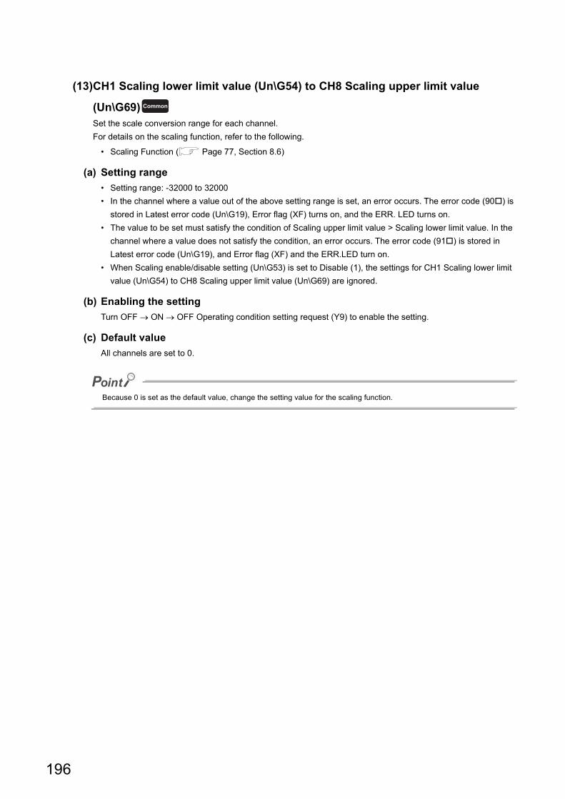
(13)CH1 Scaling lower limit value (Un\G54) to CH8 Scaling upper limit value
(Un\G69)Set the scale conversion range for each channel.
For details on the scaling function, refer to the following.
• Scaling Function ( Page 77, Section 8.6)
(a) Setting range
• Setting range: -32000 to 32000
• In the channel where a value out of the above setting range is set, an error occurs. The error code (90) is
stored in Latest error code (Un\G19), Error flag (XF) turns on, and the ERR. LED turns on.
• The value to be set must satisfy the condition of Scaling upper limit value > Scaling lower limit value. In the
channel where a value does not satisfy the condition, an error occurs. The error code (91) is stored in
Latest error code (Un\G19), and Error flag (XF) and the ERR.LED turn on.
• When Scaling enable/disable setting (Un\G53) is set to Disable (1), the settings for CH1 Scaling lower limit
value (Un\G54) to CH8 Scaling upper limit value (Un\G69) are ignored.
(b) Enabling the setting
Turn OFF ON OFF Operating condition setting request (Y9) to enable the setting.
(c) Default value
All channels are set to 0.
Because 0 is set as the default value, change the setting value for the scaling function.
Common
196
APPX
A
Ap
pe
nd
ix 2 D
eta
ils of B
uffe
r Me
mo
ry Ad
dre
sses
(14)CH1 Warning output upper limit value (Un\G86) to CH8 Warning output lower
limit value (Un\G101)Set the upper and lower limit values of the warning output range.
For details on the warning output function, refer to the following.
• Warning Output Function ( Page 83, Section 8.7)
(a) Setting range
• Setting range: -32768 to 32767
• When the scaling function is used, consider the scaling range and specify values.
• The value to be set must satisfy the condition of Warning output upper limit value > Warning output lower
limit value. In the channel where a value does not satisfy the condition, an error occurs. The error code
(62) is stored in Latest error code (Un\G19), and Error flag (XF) and the ERR.LED turn on.
• When Warning output setting (Un\G47) is set to Disable (1), the settings for CH1 Warning output upper limit
value (Un\G86) to CH8 Warning output lower limit value (Un\G101) are ignored.
(b) Enabling the setting
Turn OFF ON OFF Operating condition setting request (Y9) to enable the setting.
(c) Default value
All channels are set to 0.
Because 0 is set as the default value, change the setting value for the warning output function.
Common
197
(15)Mode switching setting (Un\G158, Un\G159)Set the setting value for the mode to be switched to.
(a) Setting procedure
Turn OFF ON OFF Operating condition setting request (Y9) to enable the setting.
(b) After the mode switching
When the mode is switched, this area is cleared to zero and Operating condition setting completed flag (X9) is
turned to OFF.
After checking that Operating condition setting completed flag (X9) is OFF, turn Operating condition setting
request (Y9) to OFF.
● Even though a value is set in this area in the wave output mode, the set value is ignored and only the operating condition is changed. (The mode cannot be switched from the normal mode to the offset/gain setting mode, and from the offset/gain setting mode to the normal mode.) To switch the mode in the wave output mode, use "Drive Mode Setting" of the switch setting.For the switch setting, refer to the following.
• Switch Setting ( Page 56, Section 7.2)
● In the following cases, the mode is not switched and only the operating condition is changed.• When a value other than the above setting values is written and Operating condition setting request (Y9) is turned
on and off• When the same setting value as the one of the current drive mode is written and Operating condition setting
request (Y9) is turned on and off
(16)Pass data classification setting (Un\G200)
This is the area for saving and restoring the offset/gain setting value in user range setting.
Specify the offset/gain setting value to be saved and restored as either voltage or current.
Mode switching toSetting value
Un\G158 Un\G159
Normal output mode 0964H 4144H
Offset/gain setting mode 4144H 0964H
Common
DA4
0 0 0 0 0 0 0 0 0 0 0 CH1CH2CH3CH40
b15 b14 b13 b12 b11 b10 b9 b8 b7 b6 b5 b0b1b2b3b4
0: Voltage
1: Current
Data for b4 to b15 are fixed to "0".
(Even when the value is set, the setting value is ignored.)
198
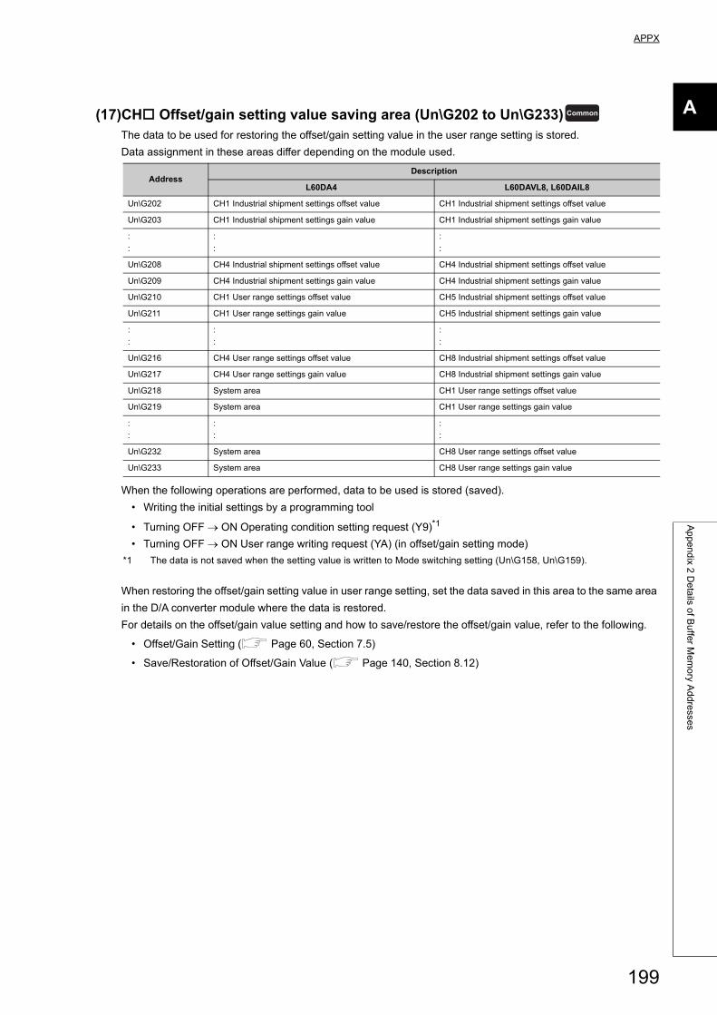
APPX
A
Ap
pe
nd
ix 2 D
eta
ils of B
uffe
r Me
mo
ry Ad
dre
sses
(17)CH Offset/gain setting value saving area (Un\G202 to Un\G233)The data to be used for restoring the offset/gain setting value in the user range setting is stored.
Data assignment in these areas differ depending on the module used.
When the following operations are performed, data to be used is stored (saved).
• Writing the initial settings by a programming tool
• Turning OFF ON Operating condition setting request (Y9)*1
• Turning OFF ON User range writing request (YA) (in offset/gain setting mode)
*1 The data is not saved when the setting value is written to Mode switching setting (Un\G158, Un\G159).
When restoring the offset/gain setting value in user range setting, set the data saved in this area to the same area
in the D/A converter module where the data is restored.
For details on the offset/gain value setting and how to save/restore the offset/gain value, refer to the following.
• Offset/Gain Setting ( Page 60, Section 7.5)
• Save/Restoration of Offset/Gain Value ( Page 140, Section 8.12)
AddressDescription
L60DA4 L60DAVL8, L60DAIL8
Un\G202 CH1 Industrial shipment settings offset value CH1 Industrial shipment settings offset value
Un\G203 CH1 Industrial shipment settings gain value CH1 Industrial shipment settings gain value
:
:
:
:
:
:
Un\G208 CH4 Industrial shipment settings offset value CH4 Industrial shipment settings offset value
Un\G209 CH4 Industrial shipment settings gain value CH4 Industrial shipment settings gain value
Un\G210 CH1 User range settings offset value CH5 Industrial shipment settings offset value
Un\G211 CH1 User range settings gain value CH5 Industrial shipment settings gain value
:
:
:
:
:
:
Un\G216 CH4 User range settings offset value CH8 Industrial shipment settings offset value
Un\G217 CH4 User range settings gain value CH8 Industrial shipment settings gain value
Un\G218 System area CH1 User range settings offset value
Un\G219 System area CH1 User range settings gain value
:
:
:
:
:
:
Un\G232 System area CH8 User range settings offset value
Un\G233 System area CH8 User range settings gain value
Common
199
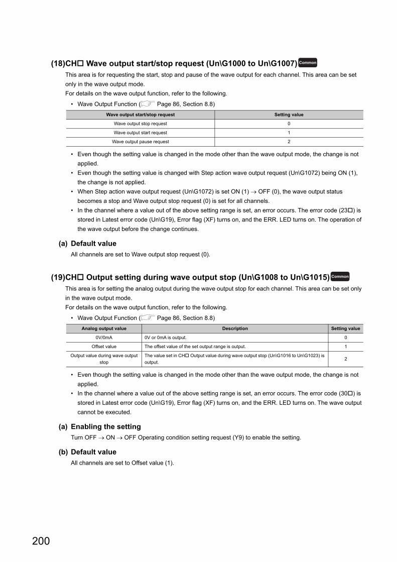
(18)CH Wave output start/stop request (Un\G1000 to Un\G1007)This area is for requesting the start, stop and pause of the wave output for each channel. This area can be set
only in the wave output mode.
For details on the wave output function, refer to the following.
• Wave Output Function ( Page 86, Section 8.8)
• Even though the setting value is changed in the mode other than the wave output mode, the change is not
applied.
• Even though the setting value is changed with Step action wave output request (Un\G1072) being ON (1),
the change is not applied.
• When Step action wave output request (Un\G1072) is set ON (1) OFF (0), the wave output status
becomes a stop and Wave output stop request (0) is set for all channels.
• In the channel where a value out of the above setting range is set, an error occurs. The error code (23) is
stored in Latest error code (Un\G19), Error flag (XF) turns on, and the ERR. LED turns on. The operation of
the wave output before the change continues.
(a) Default value
All channels are set to Wave output stop request (0).
(19)CH Output setting during wave output stop (Un\G1008 to Un\G1015)This area is for setting the analog output during the wave output stop for each channel. This area can be set only
in the wave output mode.
For details on the wave output function, refer to the following.
• Wave Output Function ( Page 86, Section 8.8)
• Even though the setting value is changed in the mode other than the wave output mode, the change is not
applied.
• In the channel where a value out of the above setting range is set, an error occurs. The error code (30) is
stored in Latest error code (Un\G19), Error flag (XF) turns on, and the ERR. LED turns on. The wave output
cannot be executed.
(a) Enabling the setting
Turn OFF ON OFF Operating condition setting request (Y9) to enable the setting.
(b) Default value
All channels are set to Offset value (1).
Wave output start/stop request Setting value
Wave output stop request 0
Wave output start request 1
Wave output pause request 2
Analog output value Description Setting value
0V/0mA 0V or 0mA is output. 0
Offset value The offset value of the set output range is output. 1
Output value during wave output
stop
The value set in CH Output value during wave output stop (Un\G1016 to Un\G1023) is
output.2
Common
Common
200
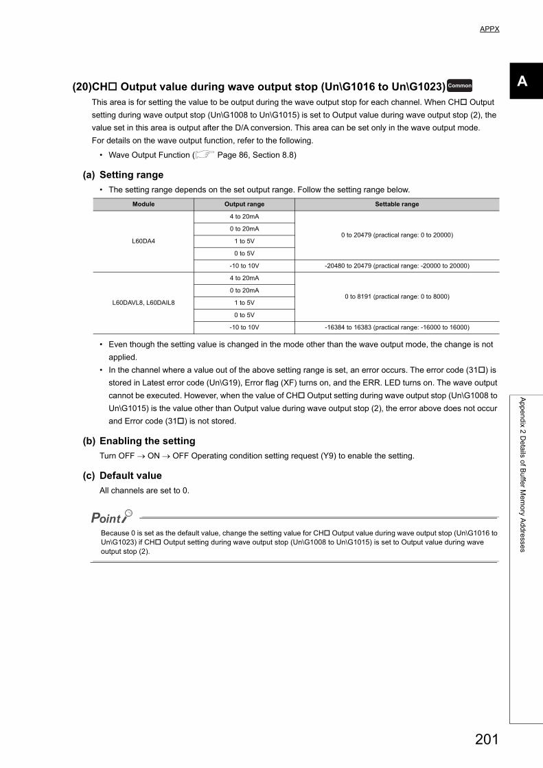
APPX
A
Ap
pe
nd
ix 2 D
eta
ils of B
uffe
r Me
mo
ry Ad
dre
sses
(20)CH Output value during wave output stop (Un\G1016 to Un\G1023)This area is for setting the value to be output during the wave output stop for each channel. When CH Output
setting during wave output stop (Un\G1008 to Un\G1015) is set to Output value during wave output stop (2), the
value set in this area is output after the D/A conversion. This area can be set only in the wave output mode.
For details on the wave output function, refer to the following.
• Wave Output Function ( Page 86, Section 8.8)
(a) Setting range
• The setting range depends on the set output range. Follow the setting range below.
• Even though the setting value is changed in the mode other than the wave output mode, the change is not
applied.
• In the channel where a value out of the above setting range is set, an error occurs. The error code (31) is
stored in Latest error code (Un\G19), Error flag (XF) turns on, and the ERR. LED turns on. The wave output
cannot be executed. However, when the value of CH Output setting during wave output stop (Un\G1008 to
Un\G1015) is the value other than Output value during wave output stop (2), the error above does not occur
and Error code (31) is not stored.
(b) Enabling the setting
Turn OFF ON OFF Operating condition setting request (Y9) to enable the setting.
(c) Default value
All channels are set to 0.
Because 0 is set as the default value, change the setting value for CH Output value during wave output stop (Un\G1016 to Un\G1023) if CH Output setting during wave output stop (Un\G1008 to Un\G1015) is set to Output value during wave output stop (2).
Module Output range Settable range
L60DA4
4 to 20mA
0 to 20479 (practical range: 0 to 20000)0 to 20mA
1 to 5V
0 to 5V
-10 to 10V -20480 to 20479 (practical range: -20000 to 20000)
L60DAVL8, L60DAIL8
4 to 20mA
0 to 8191 (practical range: 0 to 8000)0 to 20mA
1 to 5V
0 to 5V
-10 to 10V -16384 to 16383 (practical range: -16000 to 16000)
Common
201
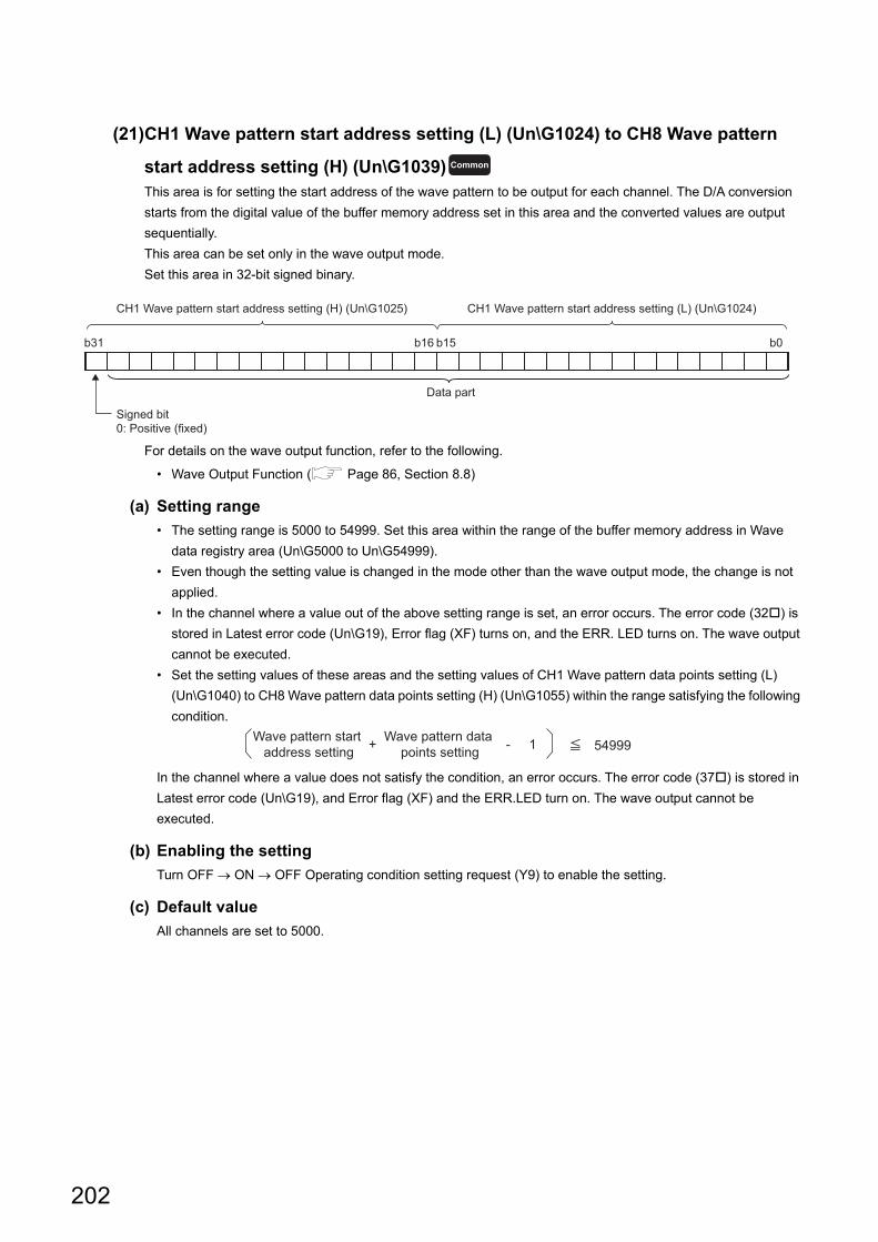
(21)CH1 Wave pattern start address setting (L) (Un\G1024) to CH8 Wave pattern
start address setting (H) (Un\G1039)This area is for setting the start address of the wave pattern to be output for each channel. The D/A conversion
starts from the digital value of the buffer memory address set in this area and the converted values are output
sequentially.
This area can be set only in the wave output mode.
Set this area in 32-bit signed binary.
For details on the wave output function, refer to the following.
• Wave Output Function ( Page 86, Section 8.8)
(a) Setting range
• The setting range is 5000 to 54999. Set this area within the range of the buffer memory address in Wave
data registry area (Un\G5000 to Un\G54999).
• Even though the setting value is changed in the mode other than the wave output mode, the change is not
applied.
• In the channel where a value out of the above setting range is set, an error occurs. The error code (32) is
stored in Latest error code (Un\G19), Error flag (XF) turns on, and the ERR. LED turns on. The wave output
cannot be executed.
• Set the setting values of these areas and the setting values of CH1 Wave pattern data points setting (L)
(Un\G1040) to CH8 Wave pattern data points setting (H) (Un\G1055) within the range satisfying the following
condition.
In the channel where a value does not satisfy the condition, an error occurs. The error code (37) is stored in
Latest error code (Un\G19), and Error flag (XF) and the ERR.LED turn on. The wave output cannot be
executed.
(b) Enabling the setting
Turn OFF ON OFF Operating condition setting request (Y9) to enable the setting.
(c) Default value
All channels are set to 5000.
Common
b15 b0
Signed bit
0: Positive (fixed)
Data part
b31 b16
CH1 Wave pattern start address setting (L) (Un\G1024)CH1 Wave pattern start address setting (H) (Un\G1025)
+ Wave pattern data points setting - 1Wave pattern start
address setting 54999
202
APPX
A
Ap
pe
nd
ix 2 D
eta
ils of B
uffe
r Me
mo
ry Ad
dre
sses
(22)CH1 Wave pattern data points setting (L) (Un\G1040) to CH8 Wave pattern data
points setting (H) (Un\G1055)This area is for setting the points of the wave pattern to be output for each channel. From the start address of the
wave pattern, the D/A conversion starts for the points of wave data set in this area and the converted values are
output. This area can be set only in the wave output mode.
Set this area in 32-bit signed binary.
For details on the wave output function, refer to the following.
• Wave Output Function ( Page 86, Section 8.8)
(a) Setting range
• The setting range is 1 to 50000. Up to the number of the data points in Wave data registry area (Un\G5000
to Un\G54999) can be set.
• Even though the setting value is changed in the mode other than the wave output mode, the change is not
applied.
• In the channel where a value out of the above setting range is set, an error occurs. The error code (33)
is stored in Latest error code (Un\G19), Error flag (XF) turns on, and the ERR. LED turns on. The wave
output cannot be executed. However, when the values of CH1 Wave pattern start address setting (L)
(Un\G1024) to CH8 Wave pattern start address setting (H) (Un\G1039) are out of the setting range, the
error above does not occur and Error code (33) is not stored.
• Set the setting values of these areas and the setting values of CH1 Wave pattern start address setting (L)
(Un\G1024) to CH8 Wave pattern start address setting (H) (Un\G1039) within the range satisfying the
following condition.
In the channel where a value does not satisfy the condition, an error occurs. The error code (37) is stored in
Latest error code (Un\G19), and Error flag (XF) and the ERR.LED turn on. The wave output cannot be
executed.
(b) Enabling the setting
Turn OFF ON OFF Operating condition setting request (Y9) to enable the setting.
(c) Default value
All channels are set to 0.
Because 0 is set as the default value, change the setting value for the wave output function.
Common
b15 b0
Signed bit
0: Positive (fixed)
Data part
b31 b16
CH1 Wave pattern data points setting (L) (Un\G1040)CH1 Wave pattern data points setting (H) (Un\G1041)
+ Wave pattern data points setting - 1Wave pattern start
address setting 54999
203
(23)CH Wave pattern output repetition setting (Un\G1056 to Un\G1063)This area is for setting the repeat count to output the wave pattern repeatedly. This area can be set only in the
wave output mode.
For details on the wave output function, refer to the following.
• Wave Output Function ( Page 86, Section 8.8)
(a) Setting range
• Follow the setting range below.
• Even though the setting value is changed in the mode other than the wave output mode, the change is not
applied.
• In the channel where a value out of the above setting range is set, an error occurs. The error code (34)
is stored in Latest error code (Un\G19), Error flag (XF) turns on, and the ERR. LED turns on. The wave
output cannot be executed.
(b) Enabling the setting
Turn OFF ON OFF Operating condition setting request (Y9) to enable the setting.
(c) Default value
All channels are set to 1.
(24)CH Constant for wave output conversion cycle (Un\G1064 to Un\G1071)Set the constant to decide the conversion cycle (specify a multiple of the conversion speed). The conversion
cycle can be set with the value set in this area under the following conditions.
This area can be set only in the wave output mode.
For details on the wave output function, refer to the following.
• Wave Output Function ( Page 86, Section 8.8)
(a) Setting range
• Setting range: 1 to 5000
• Even though the setting value is changed in the mode other than the wave output mode, the change is not
applied.
• In the channel where a value out of the above setting range is set, an error occurs. The error code (35)
is stored in Latest error code (Un\G19), Error flag (XF) turns on, and the ERR. LED turns on. The wave
output cannot be executed.
(b) Enabling the setting
Turn OFF ON OFF Operating condition setting request (Y9) to enable the setting.
(c) Default value
All channels are set to 1.
Setting value Description
-1 The wave pattern is output in analog unlimitedly.
1 to 32767 The wave pattern is output in analog for the counts of the setting value.
Common
Common
Conversion cycle ( s) Conversion speed = Number of channels whereD/A conversion is enabled
Constant for wave outputconversion cycle
204
APPX
A
Ap
pe
nd
ix 2 D
eta
ils of B
uffe
r Me
mo
ry Ad
dre
sses
(25)Step action wave output request (Un\G1072)This area is for setting whether to start or end the wave output step action function for all channels in a batch.
This area can be set only in the wave output mode.
For details on the wave output step action function, refer to the following.
• Wave output step action function ( Page 126, Section 8.8.4)
• When the setting value is changed OFF (0) ON (1), the wave output status of all the channels set to D/A
conversion enable becomes to Wave output step action and the wave output step action function becomes
valid. Wave output step action (3) is stored in CH Wave output status monitor (Un\G1100 to Un\G1107).
• When the setting value is changed ON (1) OFF (0), the wave output status of all the channels becomes to
Wave output stop and the wave output step action function ends.
• Even though the setting value is changed in the mode other than the wave output mode, the change is not
applied.
• In the channel where a value out of the above setting range is set, an error occurs. The error code (360) is
stored in Latest error code (Un\G19), Error flag (XF) turns on, and the ERR. LED turns on. The current wave
output status continues.
(a) Default value
OFF (0) is set.
Step action wave output request Setting value
OFF 0
ON 1
Common
205
(26)CH Wave output step action movement amount (Un\G1080 to
Un\G1087)This area is for setting the wave output step action movement amount and for checking the movement
completion for each channel. The currently output wave data in Wave data registry area (Un\G5000 to
Un\G54999) is changed to the data with the buffer memory address which is added or subtracted by the setting
value in this area. Setting a value in this area starts to change the data. After the change is completed, No
movement (0) is stored.
This area can be set only when the following conditions are satisfied.
• In wave output mode
• When Wave output step action (3) is stored in CH Wave output status monitor (Un\G1100 to Un\G1107)
Even though the setting value is changed not under the above conditions, the change is not applied.
For details on the wave output step action function, refer to the following.
• Wave output step action function ( Page 126, Section 8.8.4)
(a) Setting range
• Setting range: -30000 to 30000
• Set the following value according to the direction to move.
• The following shows the available movement range with CH Wave output step action movement amount
(Un\G1080 to Un\G1087).
• Even though the value which is out of the above setting range is set, no error occurs. When the value
smaller than -30000 is set, the value is processed as -30000. When the value greater than 30000 is set, the
value is processed as 30000.
(b) Default value
All channels are set to No movement (0).
Movement
directionDescription
Setting
value
No movement The buffer memory address of the wave data to be output is not moved. 0
Forward movement
The buffer memory address of the wave data to be output is moved in the address increasing direction
from the buffer memory address of the currently output wave data.
1 to 30000
Example:
When 10000 is set in CH Wave output step action movement amount (Un\G1080 to
Un\G1087) with the buffer memory address of the currently output wave data being
Un\G30000
The buffer memory address of the wave data to be output is changed to Un\G40000.
Reverse
movement
The buffer memory address of the wave data to be output is moved in the address decreasing direction
from the buffer memory address of the currently output wave data.
-1 to -30000
Example:
When -10000 is set in CH Wave output step action movement amount (Un\G1080 to
Un\G1087) with the buffer memory address of the currently output wave data being
Un\G30000
The buffer memory address of the wave data to be output is changed to Un\G20000.
Common
Wave pattern start address setting to + Wave pattern data
points setting - 1Wave pattern start
address setting
206
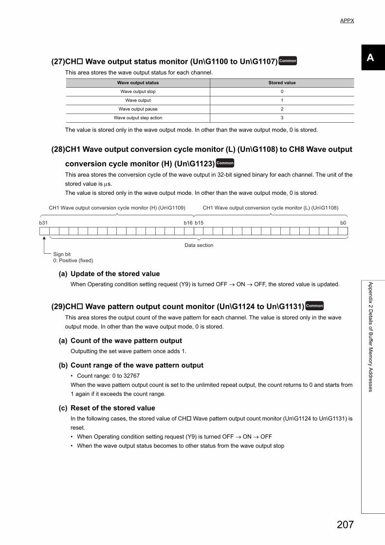
APPX
A
Ap
pe
nd
ix 2 D
eta
ils of B
uffe
r Me
mo
ry Ad
dre
sses
(27)CH Wave output status monitor (Un\G1100 to Un\G1107)This area stores the wave output status for each channel.
The value is stored only in the wave output mode. In other than the wave output mode, 0 is stored.
(28)CH1 Wave output conversion cycle monitor (L) (Un\G1108) to CH8 Wave output
conversion cycle monitor (H) (Un\G1123)This area stores the conversion cycle of the wave output in 32-bit signed binary for each channel. The unit of the
stored value is s.
The value is stored only in the wave output mode. In other than the wave output mode, 0 is stored.
(a) Update of the stored value
When Operating condition setting request (Y9) is turned OFF ON OFF, the stored value is updated.
(29)CH Wave pattern output count monitor (Un\G1124 to Un\G1131)This area stores the output count of the wave pattern for each channel. The value is stored only in the wave
output mode. In other than the wave output mode, 0 is stored.
(a) Count of the wave pattern output
Outputting the set wave pattern once adds 1.
(b) Count range of the wave pattern output
• Count range: 0 to 32767
When the wave pattern output count is set to the unlimited repeat output, the count returns to 0 and starts from
1 again if it exceeds the count range.
(c) Reset of the stored value
In the following cases, the stored value of CH Wave pattern output count monitor (Un\G1124 to Un\G1131) is
reset.
• When Operating condition setting request (Y9) is turned OFF ON OFF
• When the wave output status becomes to other status from the wave output stop
Wave output status Stored value
Wave output stop 0
Wave output 1
Wave output pause 2
Wave output step action 3
Common
Common
b15 b0
Sign bit0: Positive (fixed)
Data section
b31 b16
CH1 Wave output conversion cycle monitor (L) (Un\G1108)CH1 Wave output conversion cycle monitor (H) (Un\G1109)
Common
207
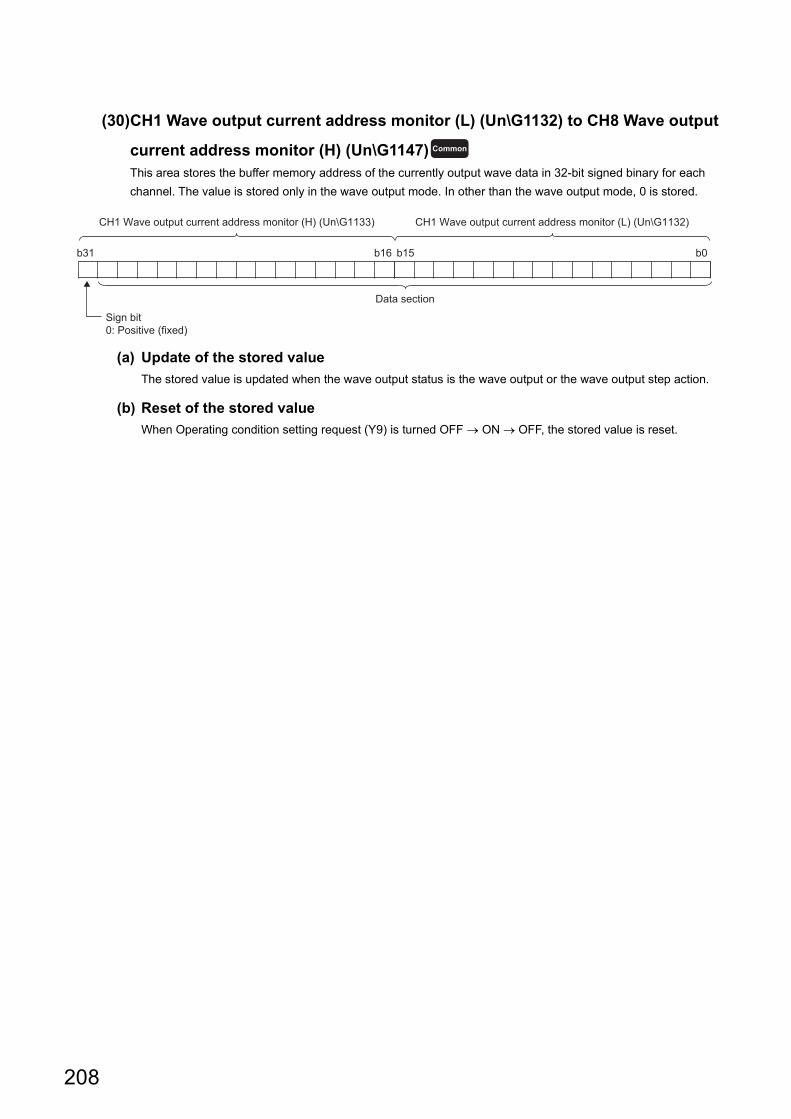
(30)CH1 Wave output current address monitor (L) (Un\G1132) to CH8 Wave output
current address monitor (H) (Un\G1147)This area stores the buffer memory address of the currently output wave data in 32-bit signed binary for each
channel. The value is stored only in the wave output mode. In other than the wave output mode, 0 is stored.
(a) Update of the stored value
The stored value is updated when the wave output status is the wave output or the wave output step action.
(b) Reset of the stored value
When Operating condition setting request (Y9) is turned OFF ON OFF, the stored value is reset.
Common
b15 b0
Sign bit0: Positive (fixed)
Data section
b31 b16
CH1 Wave output current address monitor (L) (Un\G1132)CH1 Wave output current address monitor (H) (Un\G1133)
208
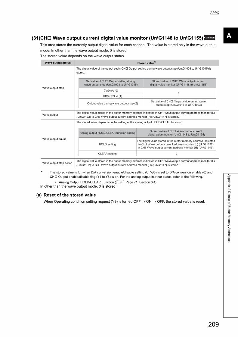
APPX
A
Ap
pe
nd
ix 2 D
eta
ils of B
uffe
r Me
mo
ry Ad
dre
sses
(31)CH Wave output current digital value monitor (Un\G1148 to Un\G1155)This area stores the currently output digital value for each channel. The value is stored only in the wave output
mode. In other than the wave output mode, 0 is stored.
The stored value depends on the wave output status.
*1 The stored value is for when D/A conversion enable/disable setting (Un\G0) is set to D/A conversion enable (0) and CH Output enable/disable flag (Y1 to Y8) is on. For the analog output in other status, refer to the following.
• Analog Output HOLD/CLEAR Function ( Page 71, Section 8.4)In other than the wave output mode, 0 is stored.
(a) Reset of the stored value
When Operating condition setting request (Y9) is turned OFF ON OFF, the stored value is reset.
Wave output status Stored value*1
Wave output stop
The digital value of the output set in CH Output setting during wave output stop (Un\G1008 to Un\G1015) is
stored.
Wave outputThe digital value stored in the buffer memory address indicated in CH1 Wave output current address monitor (L)
(Un\G1132) to CH8 Wave output current address monitor (H) (Un\G1147) is stored.
Wave output pause
The stored value depends on the setting of the analog output HOLD/CLEAR function.
Wave output step actionThe digital value stored in the buffer memory address indicated in CH1 Wave output current address monitor (L)
(Un\G1132) to CH8 Wave output current address monitor (H) (Un\G1147) is stored.
Common
0V/0mA (0)0
Offset value (1)
Output value during wave output stop (2)Set value of CH� Output value during wave
output stop (Un\G1016 to Un\G1023)
Set value of CH� Output setting during wave output stop (Un\G1008 to Un\G1015)
Stored value of CH� Wave output current digital value monitor (Un\G1148 to Un\G1155)
Analog output HOLD/CLEAR function setting Stored value of CH� Wave output current digital value monitor (Un\G1148 to Un\G1155)
HOLD setting
0CLEAR setting
The digital value stored in the buffer memory address indicated in CH1 Wave output current address monitor (L) (Un\G1132) in CH8 Wave output current address monitor (H) (Un\G1147).
209
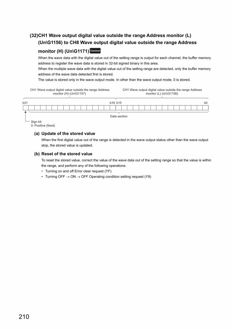
(32)CH1 Wave output digital value outside the range Address monitor (L)
(Un\G1156) to CH8 Wave output digital value outside the range Address
monitor (H) (Un\G1171)When the wave data with the digital value out of the setting range is output for each channel, the buffer memory
address to register the wave data is stored in 32-bit signed binary in this area.
When the multiple wave data with the digital value out of the setting range are detected, only the buffer memory
address of the wave data detected first is stored.
The value is stored only in the wave output mode. In other than the wave output mode, 0 is stored.
(a) Update of the stored value
When the first digital value out of the range is detected in the wave output status other than the wave output
stop, the stored value is updated.
(b) Reset of the stored value
To reset the stored value, correct the value of the wave data out of the setting range so that the value is within
the range, and perform any of the following operations.
• Turning on and off Error clear request (YF)
• Turning OFF ON OFF Operating condition setting request (Y9)
Common
b15 b0
Sign bit0: Positive (fixed)
Data section
b31 b16
CH1 Wave output digital value outside the range Addressmonitor (L) (Un\G1156)
CH1 Wave output digital value outside the range Addressmonitor (H) (Un\G1157)
210
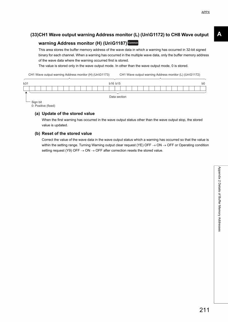
APPX
A
Ap
pe
nd
ix 2 D
eta
ils of B
uffe
r Me
mo
ry Ad
dre
sses
(33)CH1 Wave output warning Address monitor (L) (Un\G1172) to CH8 Wave output
warning Address monitor (H) (Un\G1187)This area stores the buffer memory address of the wave data in which a warning has occurred in 32-bit signed
binary for each channel. When a warning has occurred in the multiple wave data, only the buffer memory address
of the wave data where the warning occurred first is stored.
The value is stored only in the wave output mode. In other than the wave output mode, 0 is stored.
(a) Update of the stored value
When the first warning has occurred in the wave output status other than the wave output stop, the stored
value is updated.
(b) Reset of the stored value
Correct the value of the wave data in the wave output status which a warning has occurred so that the value is
within the setting range. Turning Warning output clear request (YE) OFF ON OFF or Operating condition
setting request (Y9) OFF ON OFF after correction resets the stored value.
Common
b15 b0
Sign bit0: Positive (fixed)
Data section
b31 b16
CH1 Wave output warning Address monitor (L) (Un\G1172) CH1 Wave output warning Address monitor (H) (Un\G1173)
211
(34)CH D/A conversion status (Un\G1700 to Un\G1707)
The operating status of D/A conversion is stored.
Use these areas for troubleshooting. For details, refer to the following.
• When an analog output value is not output ( Page 177, Section 11.6.2 (2))
*1 The analog output status varies depending on the CPU module status or the setting of the analog output HOLD/CLEAR function ("HOLD/CLEAR function" of "Switch Setting").For details, refer to the following.
• Combination of analog output status ( Page 71, Section 8.4 (1))*2 When the wave output function is used, the wave data is output according to the value stored in CH Wave output
status monitor (Un\G1100 to Un\G1107).For details, refer to the following.
• CH Wave output status monitor (Un\G1100 to Un\G1107) ( Page 207, Appendix 2 (27))
(35)CH Analog output command value (Un\G1710, Un\G1712, Un\G1714,
Un\G1716, Un\G1718, Un\G1720, Un\G1722, Un\G1724)
The analog value commanded to be output from the analog output circuit by the D/A converter module is stored.
This item is updated about every 1ms.
Use these areas for troubleshooting. For details, refer to the following.
• When an analog output value is not output ( Page 177, Section 11.6.2 (2))
The stored value of CH Analog output command value (Un\G1710, Un\G1712, Un\G1714, Un\G1716,
Un\G1718, Un\G1720, Un\G1722, Un\G1724) varies as follows depending on the value stored in CH D/A
conversion status (Un\G1700 to Un\G1707).
(a) For "Analog output disable (1)" and "Analog output enable (2)"
The following value is stored.
• Current output: The value obtained by the current output value [mA] 100 is stored. For 20mA output, 2000
is stored.
• Voltage output: The value obtained by the voltage output value [V] 100 is stored. For 10V output, 1000 is
stored.
(b) For "External power supply OFF (-1)" and "D/A conversion disable (0)"
The value 0 is stored.
Do not use the stored value of this item for actual control.Use the stored value of this item as a guide to check the analog output status when starting a system.
D/A conversion status Stored value Description
External power supply OFF -1 The external power supply 24VDC is not supplied.
D/A conversion disable 0D/A conversion is disabled. D/A conversion is not performed on the corresponding
channel.
Analog output disable 1 Analog output is disabled. (D/A conversion is enabled.)*1
Analog output enable 2Analog output is enabled.
Analog output is performed according to the digital value.*2
DAVL8 DAIL8
DAVL8 DAIL8
212
APPX
A
Ap
pe
nd
ix 2 D
eta
ils of B
uffe
r Me
mo
ry Ad
dre
sses
(36)CH Analog output command value unit (Un\G1711, Un\G1713, Un\G1715,
Un\G1717, Un\G1719, Un\G1721, Un\G1723, Un\G1725)
The unit of CH Analog output command value (Un\G1710, Un\G1712, Un\G1714, Un\G1716, Un\G1718,
Un\G1720, Un\G1722, Un\G1724) is stored.
Use these areas for troubleshooting. For details, refer to the following.
• When an analog output value is not output ( Page 177, Section 11.6.2 (2))
(37)RUN LED status monitor (Un\G1730)
The current RUN LED status is stored.
For details, refer to the following.
• PART NAMES ( Page 21, CHAPTER 2)
(38)ERR LED status monitor (Un\G1731)
The current ERR. LED status is stored.
For details, refer to the following.
• PART NAMES ( Page 21, CHAPTER 2)
(39)ALM LED status monitor (Un\G1732)
The current ALM LED status is stored.
For details, refer to the following.
• PART NAMES ( Page 21, CHAPTER 2)
Unit Stored value
10-2mA 0
10-2V 1
LED status Stored value Description
Off 0 Indicates that the LED is off.
On 1 Indicates that the LED is on.
Flashing (every 0.5s) 2 Indicates that the LED flashes.
LED status Stored value Description
Off 0 Indicates that the LED is off.
On 1 Indicates that the LED is on.
Flashing (every 0.5s) 2 Indicates that the LED flashes.
LED status Stored value Description
Off 0 Indicates that the LED is off.
On 1 Indicates that the LED is on.
DAVL8 DAIL8
DAVL8 DAIL8
DAVL8 DAIL8
DAVL8 DAIL8
213
(40)Latest address of error history (Un\G1800)Among Error history No. (Un\G1810 to Un\G1969), the buffer memory address where the latest error code has
been stored is stored.
(41)Error history clear setting (Un\G1802)
Set whether to clear Error history No. (Un\G1810 to Un\G1969) or not when turning on Error clear request (YF)
or Operating condition setting request (Y9).
When a value out of the above setting range is set, the module operates with the setting of Not clear (0).
(a) Default value
Not clear (0) is set.
(42)Error history No. (Un\G1810 to Un\G1969)Up to 16 errors that occurred in the module are recorded.
For details on the error log function, refer to the following.
• Error Log Function ( Page 135, Section 8.9)
*1 Those are values when an error occurs at 10:35:40 on Tuesday, March 29th, 2011.
Setting Setting value
Not clear 0
Clear 1
Item Stored data Example*1
First two digits of the year/Last
two digits of the year
Stored in BCD code.
2011H
Month/Day 0329H
Hour/Minute 1035H
Second 40H
Day of the week
The value that corresponds to the day of the week is stored in BCD code.
• Sunday: 0
• Monday: 1
• Tuesday: 2
• Wednesday: 3
• Thursday: 4
• Friday: 5
• Saturday: 6
02H
Common
DAVL8 DAIL8
Common
b15 to b8 b7 b0to
Error code
First two digits of the year Last two digits of the year
Month Day
Hour Minute
Second Day of the week
Un\G1810
Un\G1814
Un\G1813
Un\G1812
Un\G1811
Un\G1815
Un\G1819
System areato
214
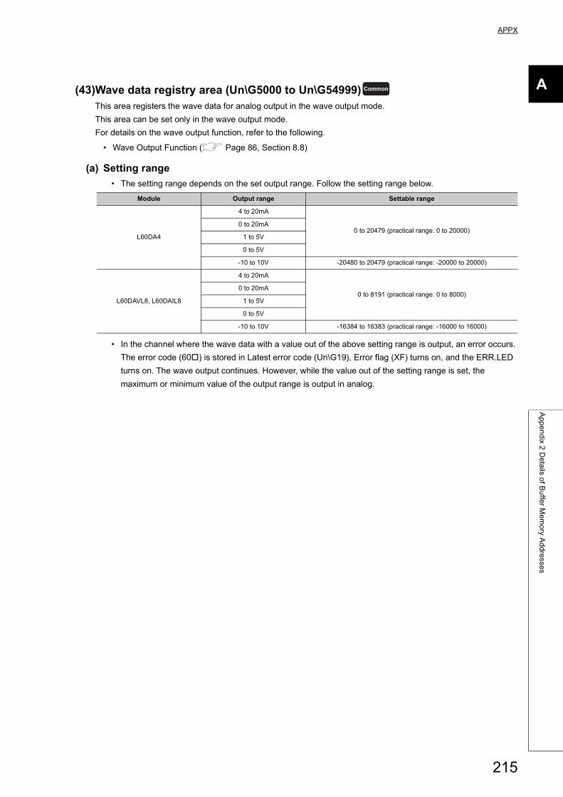
APPX
A
Ap
pe
nd
ix 2 D
eta
ils of B
uffe
r Me
mo
ry Ad
dre
sses
(43)Wave data registry area (Un\G5000 to Un\G54999)This area registers the wave data for analog output in the wave output mode.
This area can be set only in the wave output mode.
For details on the wave output function, refer to the following.
• Wave Output Function ( Page 86, Section 8.8)
(a) Setting range
• The setting range depends on the set output range. Follow the setting range below.
• In the channel where the wave data with a value out of the above setting range is output, an error occurs.
The error code (60) is stored in Latest error code (Un\G19), Error flag (XF) turns on, and the ERR.LED
turns on. The wave output continues. However, while the value out of the setting range is set, the
maximum or minimum value of the output range is output in analog.
Module Output range Settable range
L60DA4
4 to 20mA
0 to 20479 (practical range: 0 to 20000)0 to 20mA
1 to 5V
0 to 5V
-10 to 10V -20480 to 20479 (practical range: -20000 to 20000)
L60DAVL8, L60DAIL8
4 to 20mA
0 to 8191 (practical range: 0 to 8000)0 to 20mA
1 to 5V
0 to 5V
-10 to 10V -16384 to 16383 (practical range: -16000 to 16000)
Common
215
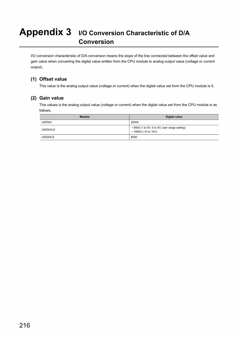
Appendix 3 I/O Conversion Characteristic of D/A Conversion
I/O conversion characteristic of D/A conversion means the slope of the line connected between the offset value and
gain value when converting the digital value written from the CPU module to analog output value (voltage or current
output).
(1) Offset valueThis value is the analog output value (voltage or current) when the digital value set from the CPU module is 0.
(2) Gain valueThis values is the analog output value (voltage or current) when the digital value set from the CPU module is as
follows.
Module Digital value
L60DA4 20000
L60DAVL8• 8000 (1 to 5V, 0 to 5V, user range setting)
• 16000 (-10 to 10V)
L60DAIL8 8000
216
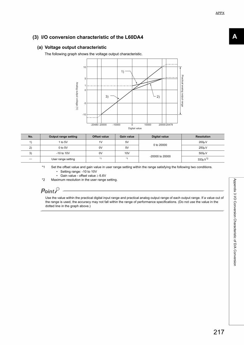
APPX
A
Ap
pe
nd
ix 3 I/O
Co
nve
rsion
Ch
ara
cteristic o
f D/A
Co
nve
rsion
(3) I/O conversion characteristic of the L60DA4
(a) Voltage output characteristic
The following graph shows the voltage output characteristic.
*1 Set the offset value and gain value in user range setting within the range satisfying the following two conditions.• Setting range: -10 to 10V• Gain value - offset value 6.6V
*2 Maximum resolution in the user range setting.
Use the value within the practical digital input range and practical analog output range of each output range. If a value out of the range is used, the accuracy may not fall within the range of performance specifications. (Do not use the value in the dotted line in the graph above.)
No. Output range setting Offset value Gain value Digital value Resolution
1) 1 to 5V 1V 5V0 to 20000
200V
2) 0 to 5V 0V 5V 250V
3) -10 to 10V 0V 10V-20000 to 20000
500V
User range setting *1 *1 333V*2
10
5
1
0
-5
-10
-20480 -20000 -10000 0 10000 20000 20479
Digital value
Pra
ctic
al a
na
log
ou
tpu
t ran
ge
1)
3) 2)
An
alo
g o
utp
ut v
olta
ge
(V)
217
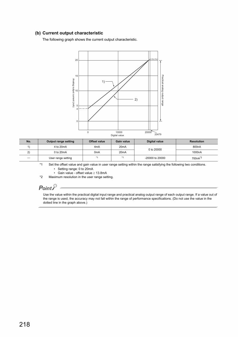
(b) Current output characteristic
The following graph shows the current output characteristic.
*1 Set the offset value and gain value in user range setting within the range satisfying the following two conditions.• Setting range: 0 to 20mA• Gain value - offset value 13.8mA
*2 Maximum resolution in the user range setting.
Use the value within the practical digital input range and practical analog output range of each output range. If a value out of the range is used, the accuracy may not fall within the range of performance specifications. (Do not use the value in the dotted line in the graph above.)
No. Output range setting Offset value Gain value Digital value Resolution
1) 4 to 20mA 4mA 20mA0 to 20000
800nA
2) 0 to 20mA 0mA 20mA 1000nA
User range setting *1 *1 -20000 to 20000 700nA*2
1)
2)
20
15
10
5
4
0
0 10000 2000020479
An
alo
g o
utp
ut c
urre
nt (m
A)
Pra
ctic
al a
na
log
ou
tpu
t ran
ge
Digital value
218
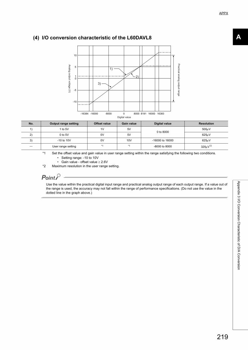
APPX
A
Ap
pe
nd
ix 3 I/O
Co
nve
rsion
Ch
ara
cteristic o
f D/A
Co
nve
rsion
(4) I/O conversion characteristic of the L60DAVL8
*1 Set the offset value and gain value in user range setting within the range satisfying the following two conditions.• Setting range: -10 to 10V• Gain value - offset value 2.6V
*2 Maximum resolution in the user range setting.
Use the value within the practical digital input range and practical analog output range of each output range. If a value out of the range is used, the accuracy may not fall within the range of performance specifications. (Do not use the value in the dotted line in the graph above.)
No. Output range setting Offset value Gain value Digital value Resolution
1) 1 to 5V 1V 5V0 to 8000
500V
2) 0 to 5V 0V 5V 625V
3) -10 to 10V 0V 10V -16000 to 16000 625V
User range setting *1 *1 -8000 to 8000 320V*2
1)
3)
2)
Practical analog output range
Digital value0 8000 16000-8000-16000
0
-5
-10
5
10
16383-16384
1
8191
Analog output voltage (V
)
219
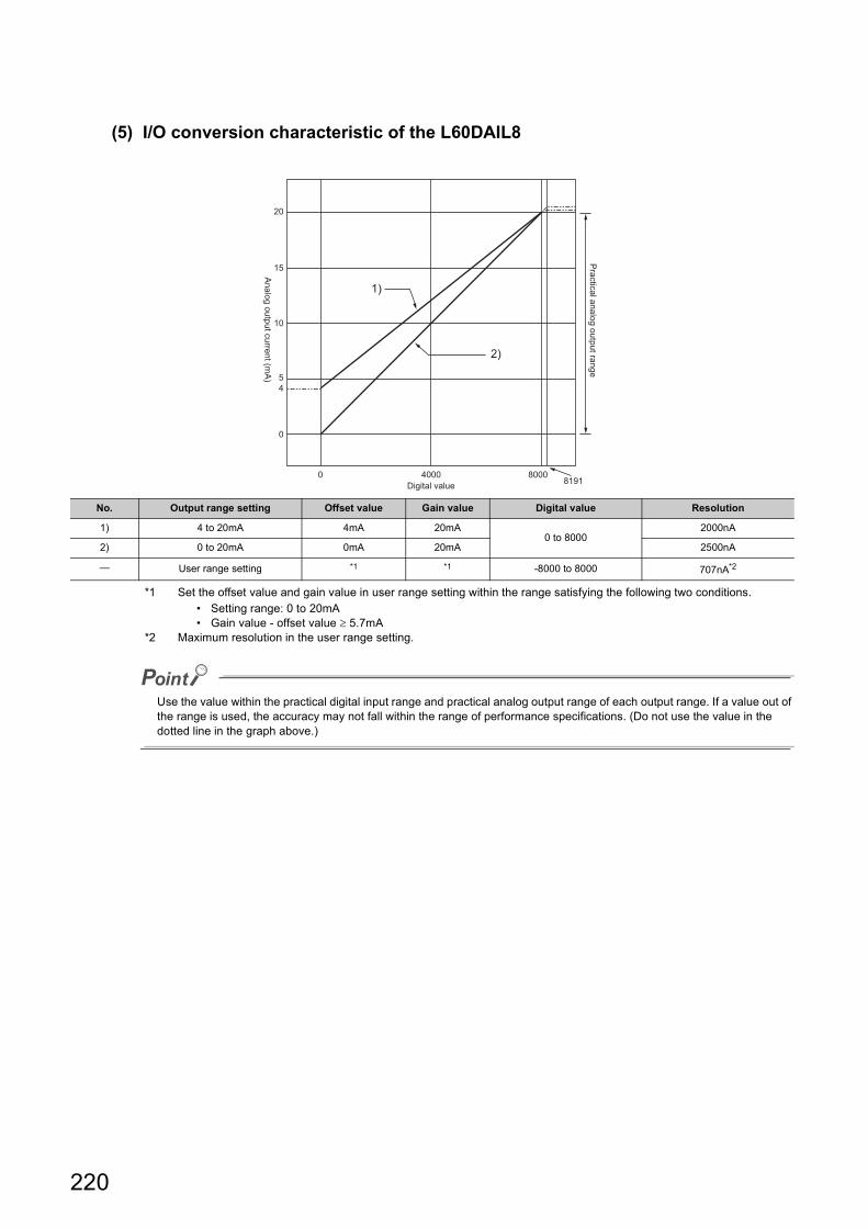
(5) I/O conversion characteristic of the L60DAIL8
*1 Set the offset value and gain value in user range setting within the range satisfying the following two conditions.• Setting range: 0 to 20mA• Gain value - offset value 5.7mA
*2 Maximum resolution in the user range setting.
Use the value within the practical digital input range and practical analog output range of each output range. If a value out of the range is used, the accuracy may not fall within the range of performance specifications. (Do not use the value in the dotted line in the graph above.)
No. Output range setting Offset value Gain value Digital value Resolution
1) 4 to 20mA 4mA 20mA0 to 8000
2000nA
2) 0 to 20mA 0mA 20mA 2500nA
User range setting *1 *1 -8000 to 8000 707nA*2
1)
2)
20
15
10
54
0
0 4000 80008191
Analog output current (m
A)
Practical analog output range
Digital value
220
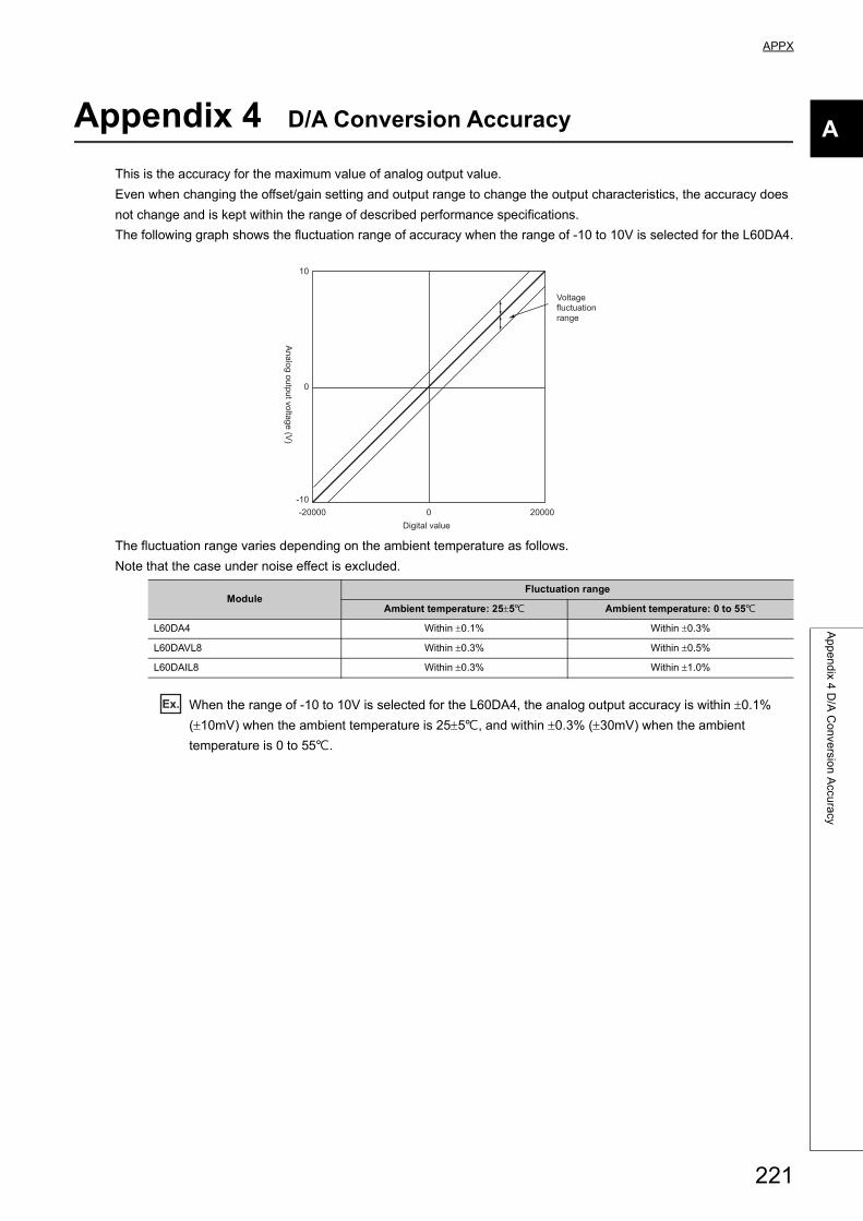
221
APPX
A
Ap
pe
nd
ix 4 D
/A C
on
versio
n A
ccura
cy
Appendix 4 D/A Conversion Accuracy
This is the accuracy for the maximum value of analog output value.
Even when changing the offset/gain setting and output range to change the output characteristics, the accuracy does
not change and is kept within the range of described performance specifications.
The following graph shows the fluctuation range of accuracy when the range of -10 to 10V is selected for the L60DA4.
The fluctuation range varies depending on the ambient temperature as follows.
Note that the case under noise effect is excluded.
Ex. When the range of -10 to 10V is selected for the L60DA4, the analog output accuracy is within 0.1%
(10mV) when the ambient temperature is 255, and within 0.3% (30mV) when the ambient
temperature is 0 to 55.
ModuleFluctuation range
Ambient temperature: 255 Ambient temperature: 0 to 55
L60DA4 Within 0.1% Within 0.3%
L60DAVL8 Within 0.3% Within 0.5%
L60DAIL8 Within 0.3% Within 1.0%
Voltage fluctuation range
Digital value
An
alo
g o
utp
ut v
olta
ge
(V)
10
0
-10
-20000 0 20000
Appendix 5 Dedicated Instruction
This chapter describes the dedicated instructions that can be used in D/A converter module.
Appendix 5.1 Instruction list
The following shows the dedicated instructions that can be used in D/A converter module.
Instruction Description
G(P).OFFGAN• The operation mode is changed from the normal output mode to the offset/gain setting mode.
• The operation mode is changed from the offset/gain setting mode to the normal output mode.
G(P).OGLOAD The offset/gain set value in the user range setting is read out to the CPU module.
G(P).OGSTORThe offset/gain set value in the user range setting stored in the CPU module is restored to the D/A converter
module.
222
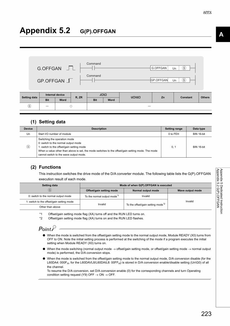
APPX
A
Ap
pe
nd
ix 5 D
ed
icate
d In
structio
nA
pp
en
dix 5
.2 G
(P).O
FF
GA
N
Appendix 5.2 G(P).OFFGAN
(1) Setting data
(2) FunctionsThis instruction switches the drive mode of the D/A converter module. The following table lists the G(P).OFFGAN
execution result of each mode.
*1 Offset/gain setting mode flag (XA) turns off and the RUN LED turns on.*2 Offset/gain setting mode flag (XA) turns on and the RUN LED flashes.
● When the mode is switched from the offset/gain setting mode to the normal output mode, Module READY (X0) turns from OFF to ON. Note the initial setting process is performed at the switching of the mode if a program executes the initial setting when Module READY (X0) turns on.
● When the mode switching (normal output mode offset/gain setting mode, or offset/gain setting mode normal output mode) is performed, the D/A conversion stops.
● When the mode is switched from the offset/gain setting mode to the normal output mode, D/A conversion disable (for the L60DA4: 000FH, for the L60DAVL8/L60DAIL8: 00FFH) is stored in D/A conversion enable/disable setting (Un\G0) of all
the channel.To resume the D/A conversion, set D/A conversion enable (0) for the corresponding channels and turn Operating condition setting request (Y9) OFF ON OFF.
Setting dataInternal device
R, ZRJ\
U\G Zn Constant OthersBit Word Bit Word
Device Description Setting range Data type
Un Start I/O number of module 0 to FEH BIN 16-bit
Switching the operation mode
0: switch to the normal output mode
1: switch to the offset/gain setting mode
When a value other than above is set, the mode switches to the offset/gain setting mode. The mode
cannot switch to the wave output mode.
0, 1 BIN 16-bit
Setting data Mode of when G(P).OFFGAN is executed
Offset/gain setting mode Normal output mode Wave output mode
0: switch to the normal output mode To the normal output mode*1 Invalid
Invalid1: switch to the offset/gain setting modeInvalid To the offset/gain setting mode*2
Other than above
Command
G.OFFGAN
Command
Un
GP.OFFGAN Un
SG.OFFGAN
GP.OFFGAN S
S
S
S
223
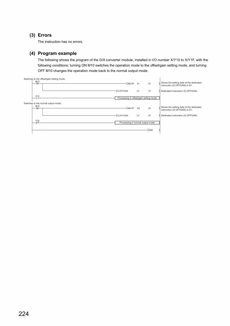
(3) ErrorsThe instruction has no errors.
(4) Program exampleThe following shows the program of the D/A converter module, installed in I/O number X/Y10 to X/Y1F, with the
following conditions: turning ON M10 switches the operation mode to the offset/gain setting mode, and turning
OFF M10 changes the operation mode back to the normal output mode.
Switches to the offset/gain setting mode.
Switches to the normal output mode.
Stores the setting data of the dedicated instruction (G.OFFGAN) in D1.
Dedicated instruction (G.OFFGAN)
Stores the setting data of the dedicated instruction (G.OFFGAN) in D1.
Dedicated instruction (G.OFFGAN)
Processing in offset/gain setting mode
Processing in normal output mode
224
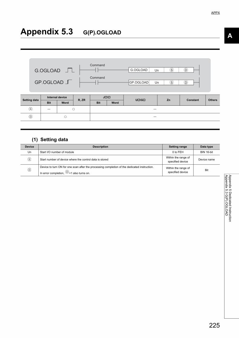
APPX
A
Ap
pe
nd
ix 5 D
ed
icate
d In
structio
nA
pp
en
dix 5
.3 G
(P).O
GL
OA
D
Appendix 5.3 G(P).OGLOAD
(1) Setting data
Setting dataInternal device
R, ZRJ\
U\G Zn Constant OthersBit Word Bit Word
Device Description Setting range Data type
Un Start I/O number of module 0 to FEH BIN 16-bit
Start number of device where the control data is storedWithin the range of
specified deviceDevice name
Device to turn ON for one scan after the processing completion of the dedicated instruction.
In error completion, +1 also turns on.
Within the range of
specified deviceBit
Command
Command
GP.OGLOAD
G.OGLOAD S D
S DGP.OGLOAD
G.OGLOAD Un
Un
S
D
S
DD
225
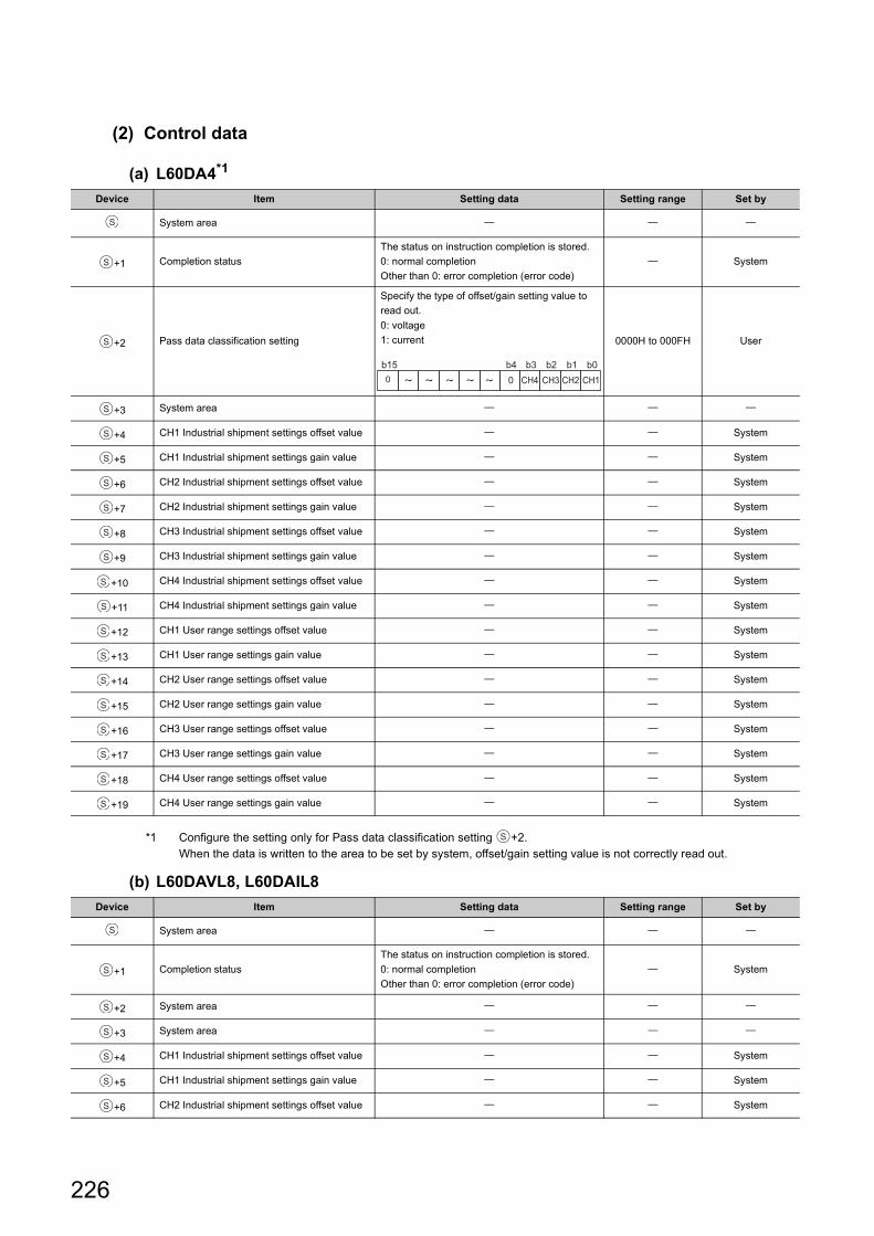
(2) Control data
(a) L60DA4*1
*1 Configure the setting only for Pass data classification setting +2.When the data is written to the area to be set by system, offset/gain setting value is not correctly read out.
(b) L60DAVL8, L60DAIL8
Device Item Setting data Setting range Set by
System area
+1 Completion status
The status on instruction completion is stored.
0: normal completion
Other than 0: error completion (error code)
System
+2 Pass data classification setting
Specify the type of offset/gain setting value to
read out.
0: voltage
1: current 0000H to 000FH User
+3 System area
+4 CH1 Industrial shipment settings offset value System
+5 CH1 Industrial shipment settings gain value System
+6 CH2 Industrial shipment settings offset value System
+7 CH2 Industrial shipment settings gain value System
+8 CH3 Industrial shipment settings offset value System
+9 CH3 Industrial shipment settings gain value System
+10 CH4 Industrial shipment settings offset value System
+11 CH4 Industrial shipment settings gain value System
+12 CH1 User range settings offset value System
+13 CH1 User range settings gain value System
+14 CH2 User range settings offset value System
+15 CH2 User range settings gain value System
+16 CH3 User range settings offset value System
+17 CH3 User range settings gain value System
+18 CH4 User range settings offset value System
+19 CH4 User range settings gain value System
Device Item Setting data Setting range Set by
System area
+1 Completion status
The status on instruction completion is stored.
0: normal completion
Other than 0: error completion (error code)
System
+2 System area
+3 System area
+4 CH1 Industrial shipment settings offset value System
+5 CH1 Industrial shipment settings gain value System
+6 CH2 Industrial shipment settings offset value System
S
S
S
0 0 CH4 CH3 CH2 CH1
b15 b3 b2 b1 b0b4
S
S
S
S
S
S
S
S
S
S
S
S
S
S
S
S
S
S
S
S
S
S
S
S
S
226
APPX
A
Ap
pe
nd
ix 5 D
ed
icate
d In
structio
nA
pp
en
dix 5
.3 G
(P).O
GL
OA
D
(3) Functions• This instruction reads out the offset/gain setting value in the user range setting of the D/A converter module
to CPU module.
• This instruction is disabled in the wave output mode.
• The interlock signal of the G(P).OGLOAD instruction includes a completion device and a completion
status indication device +1.
(a) Completion device
The device turns ON at the END processing for the scan where the G(P).OGLOAD instruction is completed,
and turns OFF at the next END processing.
+7 CH2 Industrial shipment settings gain value System
+8 CH3 Industrial shipment settings offset value System
+9 CH3 Industrial shipment settings gain value System
+10 CH4 Industrial shipment settings offset value System
+11 CH4 Industrial shipment settings gain value System
+12 CH5 Industrial shipment settings offset value System
+13 CH5 Industrial shipment settings gain value System
+14 CH6 Industrial shipment settings offset value System
+15 CH6 Industrial shipment settings gain value System
+16 CH7 Industrial shipment settings offset value System
+17 CH7 Industrial shipment settings gain value System
+18 CH8 Industrial shipment settings offset value System
+19 CH8 Industrial shipment settings gain value System
+20 CH1 User range settings offset value System
+21 CH1 User range settings gain value System
+22 CH2 User range settings offset value System
+23 CH2 User range settings gain value System
+24 CH3 User range settings offset value System
+25 CH3 User range settings gain value System
+26 CH4 User range settings offset value System
+27 CH4 User range settings gain value System
+28 CH5 User range settings offset value System
+29 CH5 User range settings gain value System
+30 CH6 User range settings offset value System
+31 CH6 User range settings gain value System
+32 CH7 User range settings offset value System
+33 CH7 User range settings gain value System
+34 CH8 User range settings offset value System
+35 CH8 User range settings gain value System
Device Item Setting data Setting range Set by
S
S
S
S
S
S
S
S
S
S
S
S
S
S
S
S
S
S
S
S
S
S
S
S
S
S
S
S
S
D
D
227
(b) Completion status indication device
This device turns OFF ON OFF depending on the status of the G(P).OGLOAD instruction completion.
• Normal completion: the device is kept to be OFF.
• Error completion: the device turns ON at the END processing for the scan where the G(P).OGLOAD
instruction is completed, and turns OFF at the next END processing.
(4) ErrorsThe instruction has no errors.
(5) Program exampleThe following shows the program to read out the offset/gain setting value of the D/A converter module, installed in
I/O number X/Y10 to X/Y1F, by turning ON M11.
*1 For the L60DAVL8 and L60DAIL8, the program in the dotted line is not required.
1 scan
ON: Execution failed
ON
ON
OFF: Execution succeeded
OFF
OFF
OFF
END processing
Program
G(P).OGLOAD
instruction
Execution completion of the
G(P).OGLOAD instruction
Completion device D
Completion status
indication device D +1
END processing
END processing
END processing
Specifies voltage.
Dedicated instruction (GP.OGLOAD)
Processing when an instruction execution is failed
Control data setting
Offset/gain value read
*1
228
APPX
A
Ap
pe
nd
ix 5 D
ed
icate
d In
structio
nA
pp
en
dix 5
.4 G
(P).O
GS
TO
R
Appendix 5.4 G(P).OGSTOR
(1) Setting data
*1 Specify the device specified to on execution of the G(P).OGLOAD instruction.Do not change the data which is read out by the G(P).OGLOAD instruction. If the data is changed, the normal operation may not be ensured.
Setting dataInternal device
R, ZRJ\
U\G ZnConstant
K, H, $ Others
Bit Word Bit Word
Device Description Setting range Data type
Un Start I/O number of module 0 to FEH BIN 16-bit
*1 Start number of device where the control data is storedWithin the range of
specified deviceDevice name
Device to turn ON for one scan after the processing completion of the dedicated instruction.
In error completion, +1 also turns on.
Within the range of
specified deviceBit
Command
Command
GP.OGSTOR
G.OGSTOR S D
S DGP.OGSTOR
G.OGSTOR Un
Un
S
D
S
DD
S
229
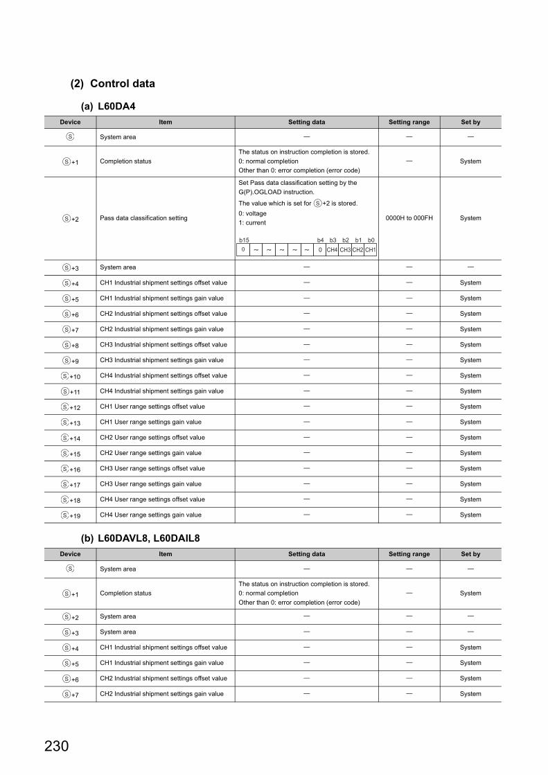
(2) Control data
(a) L60DA4
(b) L60DAVL8, L60DAIL8
Device Item Setting data Setting range Set by
System area
+1 Completion status
The status on instruction completion is stored.
0: normal completion
Other than 0: error completion (error code)
System
+2 Pass data classification setting
Set Pass data classification setting by the
G(P).OGLOAD instruction.
The value which is set for +2 is stored.
0: voltage
1: current0000H to 000FH System
+3 System area
+4 CH1 Industrial shipment settings offset value System
+5 CH1 Industrial shipment settings gain value System
+6 CH2 Industrial shipment settings offset value System
+7 CH2 Industrial shipment settings gain value System
+8 CH3 Industrial shipment settings offset value System
+9 CH3 Industrial shipment settings gain value System
+10 CH4 Industrial shipment settings offset value System
+11 CH4 Industrial shipment settings gain value System
+12 CH1 User range settings offset value System
+13 CH1 User range settings gain value System
+14 CH2 User range settings offset value System
+15 CH2 User range settings gain value System
+16 CH3 User range settings offset value System
+17 CH3 User range settings gain value System
+18 CH4 User range settings offset value System
+19 CH4 User range settings gain value System
Device Item Setting data Setting range Set by
System area
+1 Completion status
The status on instruction completion is stored.
0: normal completion
Other than 0: error completion (error code)
System
+2 System area
+3 System area
+4 CH1 Industrial shipment settings offset value System
+5 CH1 Industrial shipment settings gain value System
+6 CH2 Industrial shipment settings offset value System
+7 CH2 Industrial shipment settings gain value System
S
S
S
S
0 0 CH4 CH3 CH2 CH1
b15 b3 b2 b1 b0b4
S
S
S
S
S
S
S
S
S
S
S
S
S
S
S
S
S
S
S
S
S
S
S
S
S
230
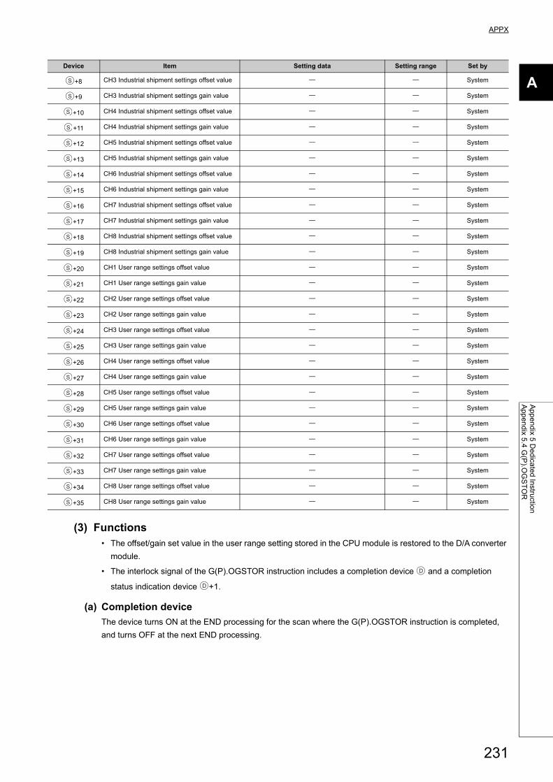
APPX
A
Ap
pe
nd
ix 5 D
ed
icate
d In
structio
nA
pp
en
dix 5
.4 G
(P).O
GS
TO
R
(3) Functions• The offset/gain set value in the user range setting stored in the CPU module is restored to the D/A converter
module.
• The interlock signal of the G(P).OGSTOR instruction includes a completion device and a completion
status indication device +1.
(a) Completion device
The device turns ON at the END processing for the scan where the G(P).OGSTOR instruction is completed,
and turns OFF at the next END processing.
+8 CH3 Industrial shipment settings offset value System
+9 CH3 Industrial shipment settings gain value System
+10 CH4 Industrial shipment settings offset value System
+11 CH4 Industrial shipment settings gain value System
+12 CH5 Industrial shipment settings offset value System
+13 CH5 Industrial shipment settings gain value System
+14 CH6 Industrial shipment settings offset value System
+15 CH6 Industrial shipment settings gain value System
+16 CH7 Industrial shipment settings offset value System
+17 CH7 Industrial shipment settings gain value System
+18 CH8 Industrial shipment settings offset value System
+19 CH8 Industrial shipment settings gain value System
+20 CH1 User range settings offset value System
+21 CH1 User range settings gain value System
+22 CH2 User range settings offset value System
+23 CH2 User range settings gain value System
+24 CH3 User range settings offset value System
+25 CH3 User range settings gain value System
+26 CH4 User range settings offset value System
+27 CH4 User range settings gain value System
+28 CH5 User range settings offset value System
+29 CH5 User range settings gain value System
+30 CH6 User range settings offset value System
+31 CH6 User range settings gain value System
+32 CH7 User range settings offset value System
+33 CH7 User range settings gain value System
+34 CH8 User range settings offset value System
+35 CH8 User range settings gain value System
Device Item Setting data Setting range Set by
S
S
S
S
S
S
S
S
S
S
S
S
S
S
S
S
S
S
S
S
S
S
S
S
S
S
S
S
D
D
231
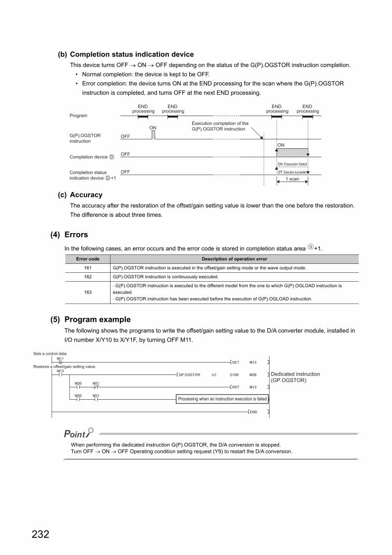
(b) Completion status indication device
This device turns OFF ON OFF depending on the status of the G(P).OGSTOR instruction completion.
• Normal completion: the device is kept to be OFF.
• Error completion: the device turns ON at the END processing for the scan where the G(P).OGSTOR
instruction is completed, and turns OFF at the next END processing.
(c) Accuracy
The accuracy after the restoration of the offset/gain setting value is lower than the one before the restoration.
The difference is about three times.
(4) Errors
In the following cases, an error occurs and the error code is stored in completion status area +1.
(5) Program exampleThe following shows the programs to write the offset/gain setting value to the D/A converter module, installed in
I/O number X/Y10 to X/Y1F, by turning OFF M11.
When performing the dedicated instruction G(P).OGSTOR, the D/A conversion is stopped.Turn OFF ON OFF Operating condition setting request (Y9) to restart the D/A conversion.
Error code Description of operation error
161 G(P).OGSTOR instruction is executed in the offset/gain setting mode or the wave output mode.
162 G(P).OGSTOR instruction is continuously executed.
163
G(P).OGSTOR instruction is executed to the different model from the one to which G(P).OGLOAD instruction is
executed.
G(P).OGSTOR instruction has been executed before the execution of G(P).OGLOAD instruction.
1 scan
ON: Execution failed
ON
ON
OFF: Execution succeeded
OFF
OFF
OFF
END processing
Program
G(P).OGSTOR
instruction
Execution completion of the
G(P).OGSTOR instruction
Completion device D
Completion status
indication device D +1
END processing
END processing
END processing
S
Dedicated instruction
(GP.OGSTOR)
Processing when an instruction execution is failed
Restores a offset/gain setting value.
Sets a control data.
232
233
APPX
A
Ap
pe
nd
ix 6 C
he
cking
Se
rial N
um
be
r an
d F
un
ction
Ve
rsion
Appendix 6 Checking Serial Number and Function Version
For details on how to check the serial number and function version, refer to the following.
MELSEC-L CPU Module User's Manual (Hardware Design, Maintenance and Inspection)
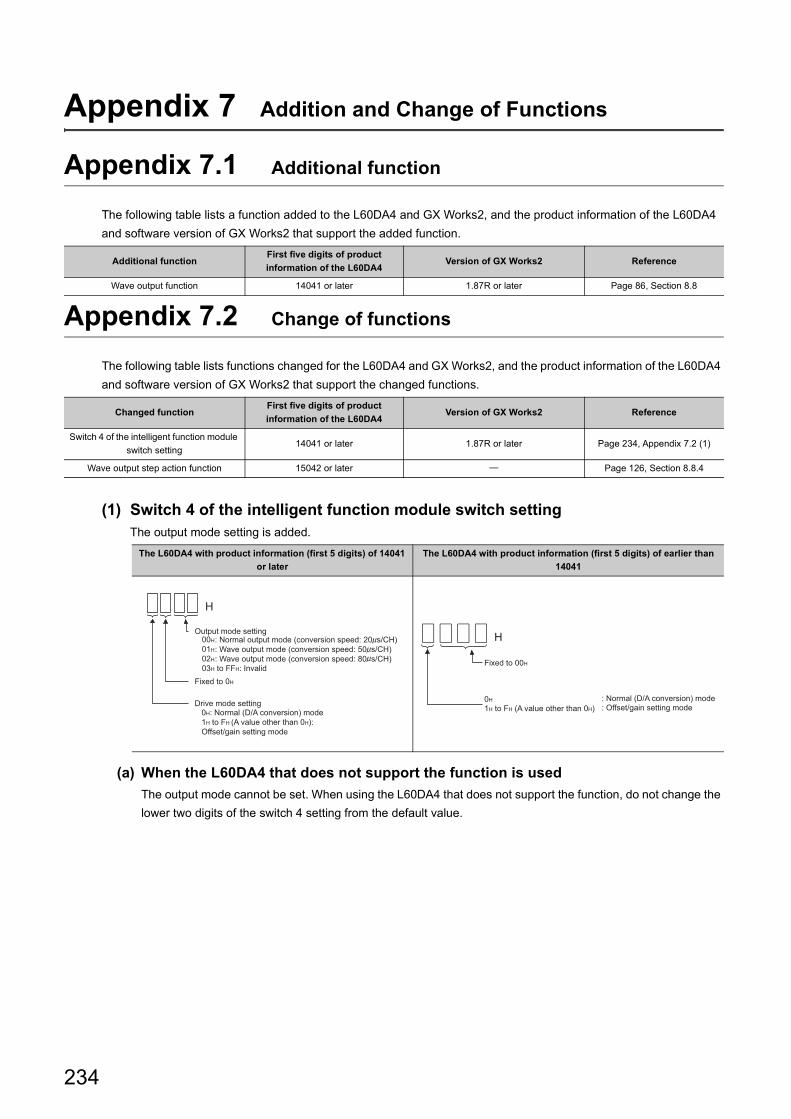
Appendix 7 Addition and Change of Functions
Appendix 7.1 Additional function
The following table lists a function added to the L60DA4 and GX Works2, and the product information of the L60DA4
and software version of GX Works2 that support the added function.
Appendix 7.2 Change of functions
The following table lists functions changed for the L60DA4 and GX Works2, and the product information of the L60DA4
and software version of GX Works2 that support the changed functions.
(1) Switch 4 of the intelligent function module switch settingThe output mode setting is added.
(a) When the L60DA4 that does not support the function is used
The output mode cannot be set. When using the L60DA4 that does not support the function, do not change the
lower two digits of the switch 4 setting from the default value.
Additional functionFirst five digits of product
information of the L60DA4Version of GX Works2 Reference
Wave output function 14041 or later 1.87R or later Page 86, Section 8.8
Changed functionFirst five digits of product
information of the L60DA4Version of GX Works2 Reference
Switch 4 of the intelligent function module
switch setting14041 or later 1.87R or later Page 234, Appendix 7.2 (1)
Wave output step action function 15042 or later Page 126, Section 8.8.4
The L60DA4 with product information (first 5 digits) of 14041
or later
The L60DA4 with product information (first 5 digits) of earlier than
14041
H
00H
01H
02H
03H to FFH: Invalid
: Normal output mode (conversion speed: 20 s/CH): Wave output mode (conversion speed: 50 s/CH): Wave output mode (conversion speed: 80 s/CH)
0H: Normal (D/A conversion) mode1H to FH (A value other than 0H):Offset/gain setting mode
Fixed to 0H
Output mode setting
Drive mode setting
H
Fixed to 00H
0H
1H to FH (A value other than 0H)
: Normal (D/A conversion) mode: Offset/gain setting mode
234
APPX
A
Ap
pe
nd
ix 7 A
dd
ition
an
d C
ha
ng
e o
f Fu
nctio
ns
Ap
pe
nd
ix 7.2
Ch
an
ge
of fu
nctio
ns
(2) Wave output step action functionA change in digital value of the currently output wave data can be easily reflected to the analog output by using
CH Wave output step action movement amount (Un\G1080 to Un\G1083) in combination with CH Output
enable/disable flag (Y1 to Y4) during the wave output step action.
The following shows the procedure.
1. Turn on and off CH Output enable/disable flag (Y1 to Y4).
2. Change the digital value of the currently output wave data to the digital value corresponding to an
analog value to be output.
3. Turn off and on CH Output enable/disable flag (Y1 to Y4).
(a) When the L60DA4 that does not support the function is used
Perform the following procedure to change the digital value of the currently output wave data and reflect the
change to the analog output.
1. Turn on and off CH Output enable/disable flag (Y1 to Y4).
2. Set a value in CH Wave output step action movement amount (Un\G1080 to Un\G1083) to move
to another wave data.
3. Change the digital value of the output wave data before the movement to the digital value
corresponding to an analog value to be output.
4. Set a value in CH Wave output step action movement amount (Un\G1080 to Un\G1083) to move
to an address of the wave data after the change.
5. Turn off and on CH Output enable/disable flag (Y1 to Y4).
235
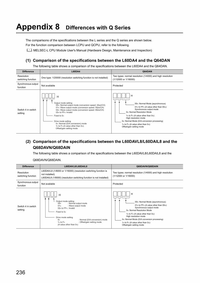
236
Appendix 8 Differences with Q Series
The comparisons of the specifications between the L series and the Q series are shown below.
For the function comparison between LCPU and QCPU, refer to the following.
MELSEC-L CPU Module User's Manual (Hardware Design, Maintenance and Inspection)
(1) Comparison of the specifications between the L60DA4 and the Q64DANThe following table shows a comparison of the specifications between the L60DA4 and the Q64DAN.
(2) Comparison of the specifications between the L60DAVL8/L60DAIL8 and the
Q68DAVN/Q68DAINThe following table shows a comparison of the specifications between the L60DAVL8/L60DAIL8 and the
Q68DAVN/Q68DAIN.
Difference L60DA4 Q64DAN
Resolution
switching functionOne type: 1/20000 (resolution switching function is not installed)
Two types: normal resolution (1/4000) and high resolution
(1/12000 or 1/16000)
Synchronous output
functionNot available Protected
Switch 4 in switch
setting
Difference L60DAVL8/L60DAIL8 Q68DAVN/Q68DAIN
Resolution
switching function
L60DAVL8 (1/8000 or 1/16000) (resolution switching function is
not installed)
L60DAIL8 (1/8000) (resolution switching function is not installed)
Two types: normal resolution (1/4000) and high resolution
(1/12000 or 1/16000)
Synchronous output
functionNot available Protected
Switch 4 in switch
setting
H
00H
01H
02H
03H to FFH: Invalid
: Normal output mode (conversion speed: 20 s/CH): Wave output mode (conversion speed: 50 s/CH): Wave output mode (conversion speed: 80 s/CH)
0H: Normal (D/A conversion) mode1H to FH (A value other than 0H):Offset/gain setting mode
Fixed to 0H
Output mode setting
Drive mode setting
H
1H to FH (A value other than 0H): Offset/gain setting mode
1H to FH (A value other than 0H): High resolution mode
0H: Normal Mode (D/A conversion processing)
0H: Normal Resolution Mode
00H: Normal Mode (asynchronous)01H to FFH (A value other than 00H): Synchronous output mode
H
00H
01H
02H to FFH
: Normal output mode : Wave output mode: Invalid
0H
1H to FH (A value other than 0H)
Fixed to 0H
Output mode setting
Drive mode setting: Normal (D/A conversion) mode: Offset/gain setting mode
H
1H to FH (A value other than 0H): Offset/gain setting mode
1H to FH (A value other than 0H): High resolution mode
0H: Normal Mode (D/A conversion processing)
0H: Normal Resolution Mode
00H: Normal Mode (asynchronous)01H to FFH (A value other than 00H): Synchronous output mode
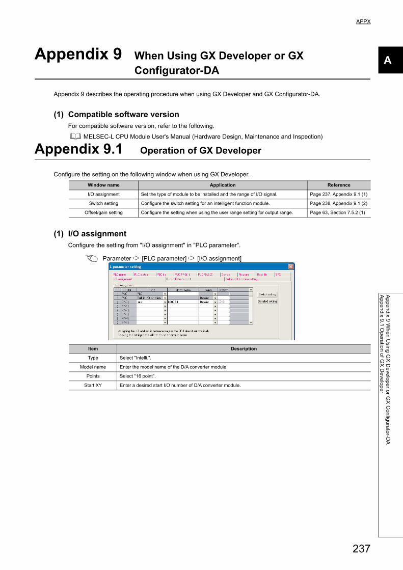
APPX
A
Ap
pe
nd
ix 9 W
he
n U
sing
GX
De
velo
pe
r or G
X C
on
figu
rato
r-DA
Ap
pe
nd
ix 9.1
Op
era
tion
of G
X D
eve
lop
er
Appendix 9 When Using GX Developer or GX Configurator-DA
Appendix 9 describes the operating procedure when using GX Developer and GX Configurator-DA.
(1) Compatible software versionFor compatible software version, refer to the following.
MELSEC-L CPU Module User's Manual (Hardware Design, Maintenance and Inspection)
Appendix 9.1 Operation of GX Developer
Configure the setting on the following window when using GX Developer.
(1) I/O assignmentConfigure the setting from "I/O assignment" in "PLC parameter".
Parameter [PLC parameter] [I/O assignment]
Window name Application Reference
I/O assignment Set the type of module to be installed and the range of I/O signal. Page 237, Appendix 9.1 (1)
Switch setting Configure the switch setting for an intelligent function module. Page 238, Appendix 9.1 (2)
Offset/gain setting Configure the setting when using the user range setting for output range. Page 63, Section 7.5.2 (1)
Item Description
Type Select "Intelli.".
Model name Enter the model name of the D/A converter module.
Points Select "16 point".
Start XY Enter a desired start I/O number of D/A converter module.
237
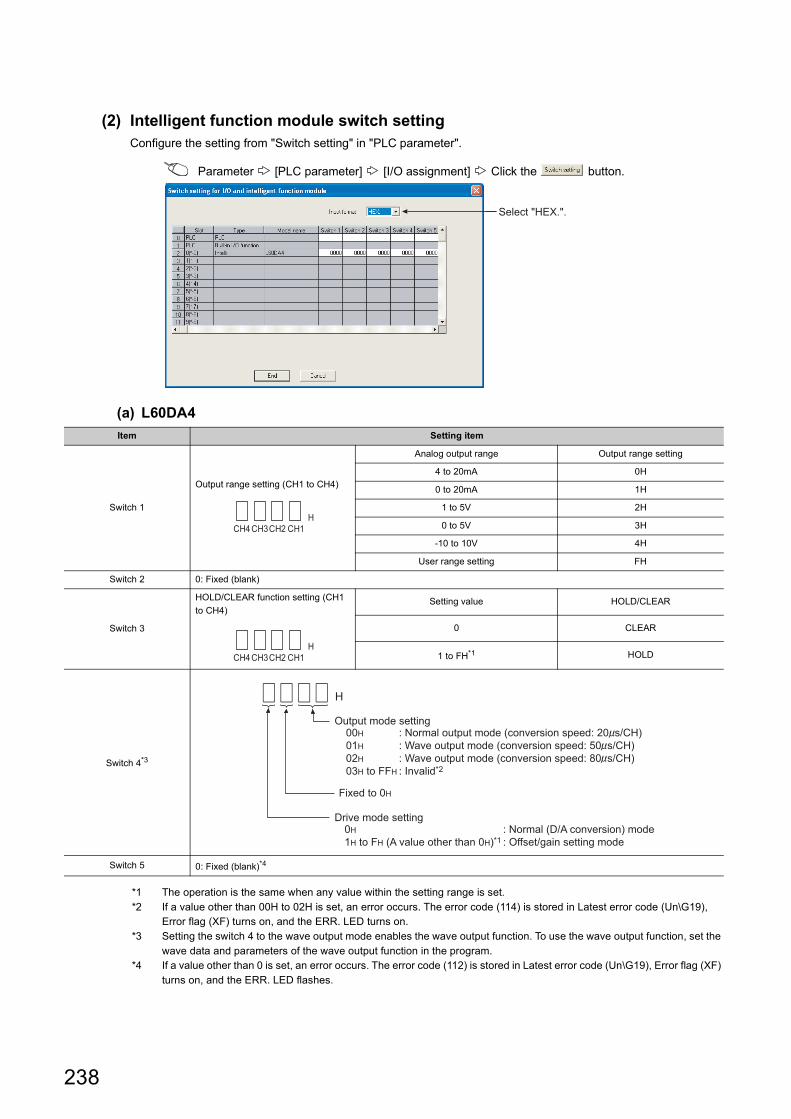
(2) Intelligent function module switch settingConfigure the setting from "Switch setting" in "PLC parameter".
Parameter [PLC parameter] [I/O assignment] Click the button.
(a) L60DA4
*1 The operation is the same when any value within the setting range is set.*2 If a value other than 00H to 02H is set, an error occurs. The error code (114) is stored in Latest error code (Un\G19),
Error flag (XF) turns on, and the ERR. LED turns on.*3 Setting the switch 4 to the wave output mode enables the wave output function. To use the wave output function, set the
wave data and parameters of the wave output function in the program.*4 If a value other than 0 is set, an error occurs. The error code (112) is stored in Latest error code (Un\G19), Error flag (XF)
turns on, and the ERR. LED flashes.
Item Setting item
Switch 1
Output range setting (CH1 to CH4)
Analog output range Output range setting
4 to 20mA 0H
0 to 20mA 1H
1 to 5V 2H
0 to 5V 3H
-10 to 10V 4H
User range setting FH
Switch 2 0: Fixed (blank)
Switch 3
HOLD/CLEAR function setting (CH1
to CH4)Setting value HOLD/CLEAR
0 CLEAR
1 to FH*1 HOLD
Switch 4*3
Switch 5 0: Fixed (blank)*4
Select "HEX.".
CH4 CH3CH2 CH1
H
CH4 CH3CH2 CH1
H
H
00H01H02H03H to FFH
: Normal output mode (conversion speed: 20 s/CH): Wave output mode (conversion speed: 50 s/CH): Wave output mode (conversion speed: 80 s/CH): Invalid*2
Fixed to 0H
Output mode setting
Drive mode setting0H1H to FH (A value other than 0H)*1
: Normal (D/A conversion) mode: Offset/gain setting mode
238
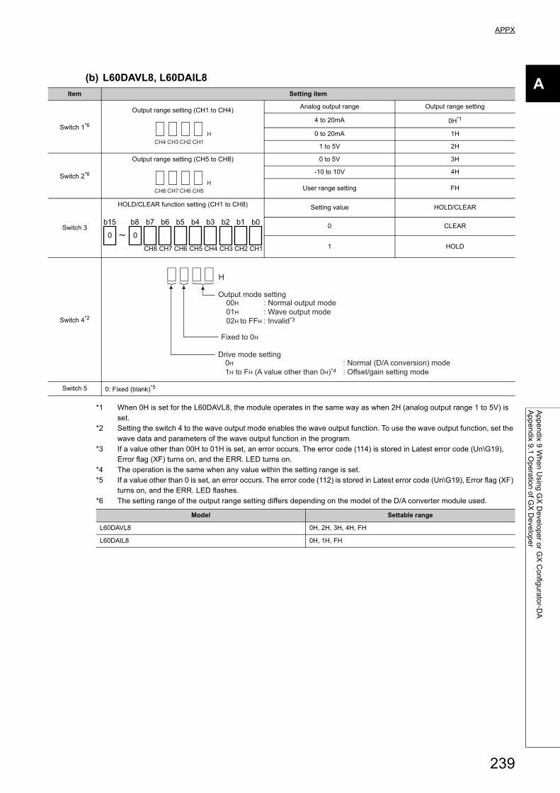
APPX
A
Ap
pe
nd
ix 9 W
he
n U
sing
GX
De
velo
pe
r or G
X C
on
figu
rato
r-DA
Ap
pe
nd
ix 9.1
Op
era
tion
of G
X D
eve
lop
er
(b) L60DAVL8, L60DAIL8
*1 When 0H is set for the L60DAVL8, the module operates in the same way as when 2H (analog output range 1 to 5V) is set.
*2 Setting the switch 4 to the wave output mode enables the wave output function. To use the wave output function, set the wave data and parameters of the wave output function in the program.
*3 If a value other than 00H to 01H is set, an error occurs. The error code (114) is stored in Latest error code (Un\G19), Error flag (XF) turns on, and the ERR. LED turns on.
*4 The operation is the same when any value within the setting range is set.*5 If a value other than 0 is set, an error occurs. The error code (112) is stored in Latest error code (Un\G19), Error flag (XF)
turns on, and the ERR. LED flashes.*6 The setting range of the output range setting differs depending on the model of the D/A converter module used.
Item Setting item
Switch 1*6
Output range setting (CH1 to CH4)Analog output range Output range setting
4 to 20mA 0H*1
0 to 20mA 1H
1 to 5V 2H
Switch 2*6
Output range setting (CH5 to CH8) 0 to 5V 3H
-10 to 10V 4H
User range setting FH
Switch 3
HOLD/CLEAR function setting (CH1 to CH8) Setting value HOLD/CLEAR
0 CLEAR
1 HOLD
Switch 4*2
Switch 5 0: Fixed (blank)*5
Model Settable range
L60DAVL8 0H, 2H, 3H, 4H, FH
L60DAIL8 0H, 1H, FH
CH4 CH3 CH2 CH1H
CH8 CH7 CH6 CH5H
CH4 CH3 CH2 CH1CH8 CH7 CH6 CH5
0 0
b0b1b2b3b4b5b6b7b8b15
H
00H01H02H to FFH
: Normal output mode: Wave output mode : Invalid*3
Fixed to 0H
Output mode setting
Drive mode setting0H1H to FH (A value other than 0H)*4
: Normal (D/A conversion) mode: Offset/gain setting mode
239
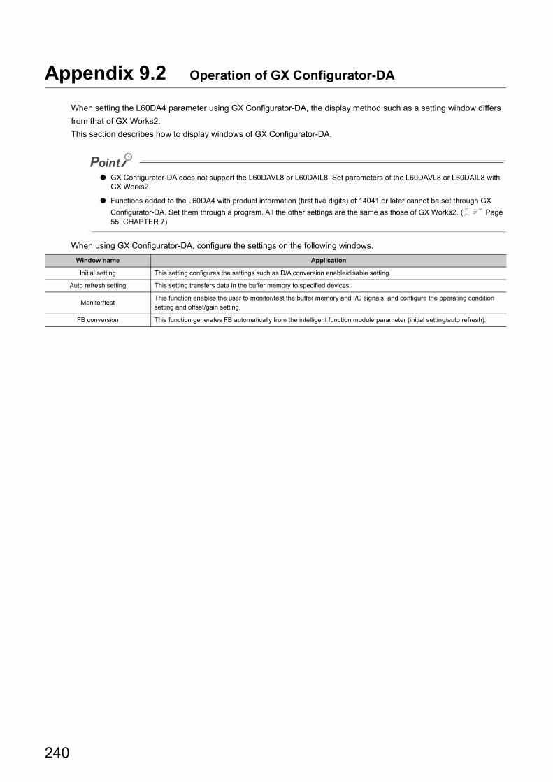
Appendix 9.2 Operation of GX Configurator-DA
When setting the L60DA4 parameter using GX Configurator-DA, the display method such as a setting window differs
from that of GX Works2.
This section describes how to display windows of GX Configurator-DA.
● GX Configurator-DA does not support the L60DAVL8 or L60DAIL8. Set parameters of the L60DAVL8 or L60DAIL8 with GX Works2.
● Functions added to the L60DA4 with product information (first five digits) of 14041 or later cannot be set through GX
Configurator-DA. Set them through a program. All the other settings are the same as those of GX Works2. ( Page 55, CHAPTER 7)
When using GX Configurator-DA, configure the settings on the following windows.
Window name Application
Initial setting This setting configures the settings such as D/A conversion enable/disable setting.
Auto refresh setting This setting transfers data in the buffer memory to specified devices.
Monitor/testThis function enables the user to monitor/test the buffer memory and I/O signals, and configure the operating condition
setting and offset/gain setting.
FB conversion This function generates FB automatically from the intelligent function module parameter (initial setting/auto refresh).
240
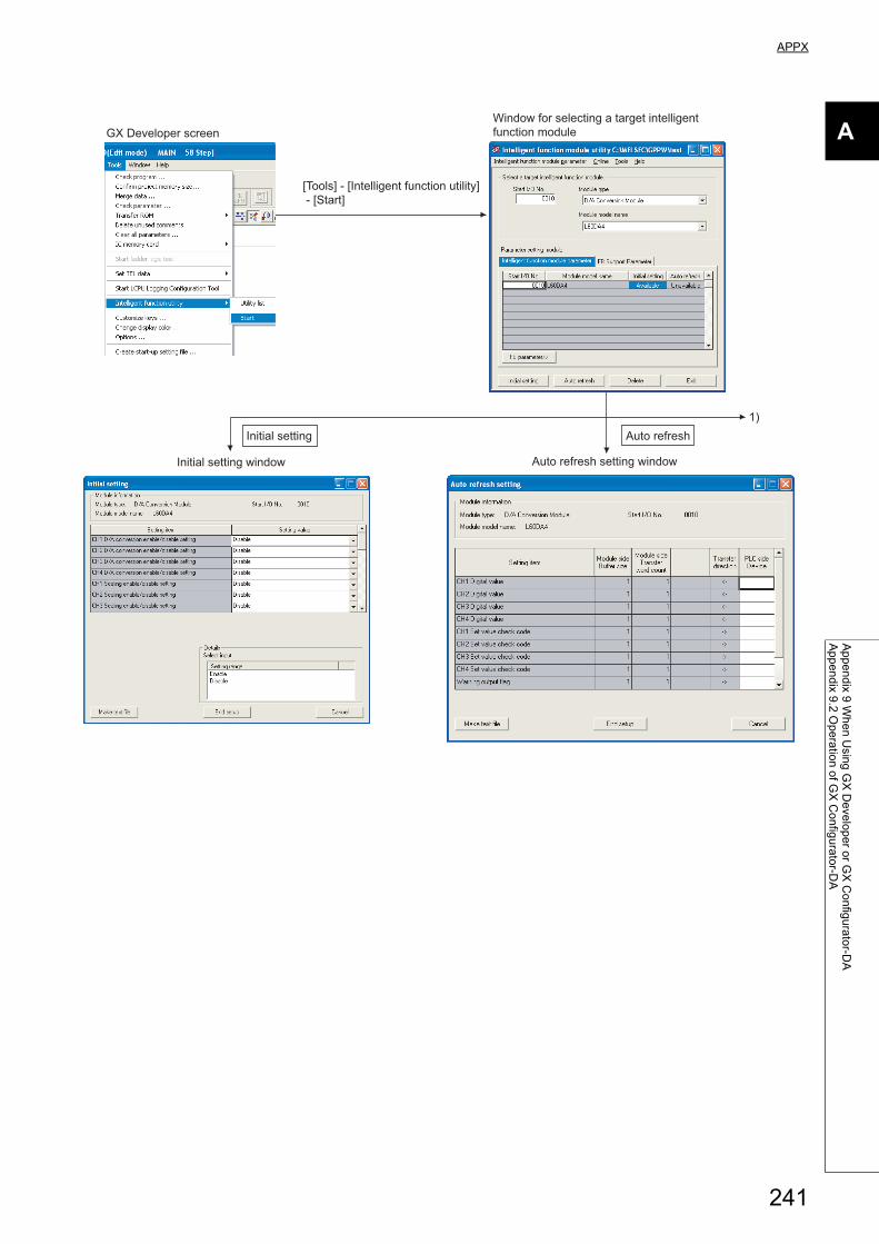
APPX
A
Ap
pe
nd
ix 9 W
he
n U
sing
GX
De
velo
pe
r or G
X C
on
figu
rato
r-DA
Ap
pe
nd
ix 9.2
Op
era
tion
of G
X C
on
figu
rato
r-DA
Initial setting window
Initial setting Auto refresh
Auto refresh setting window
1)
GX Developer screen
[Tools] - [Intelligent function utility]
- [Start]
Window for selecting a target intelligent
function module
241
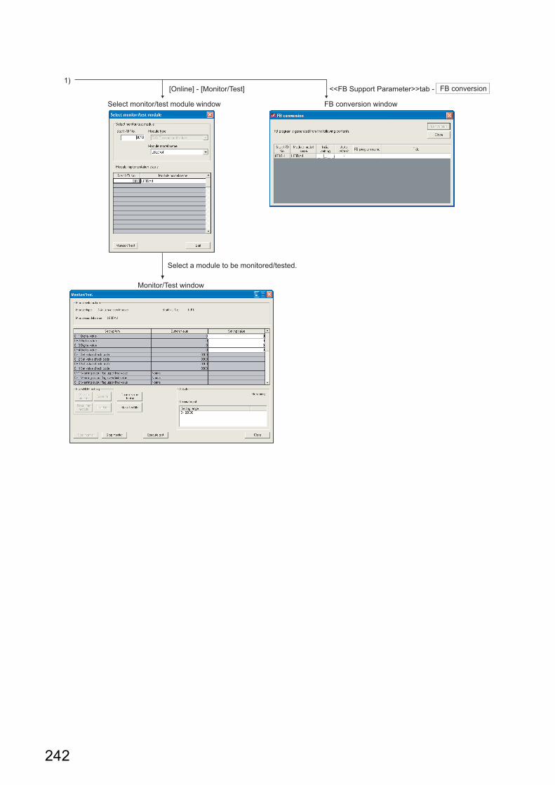
[Online] - [Monitor/Test]
Select monitor/test module window
Monitor/Test window
Select a module to be monitored/tested.
1)
FB conversion window
<<FB Support Parameter>>tab - FB conversion
242
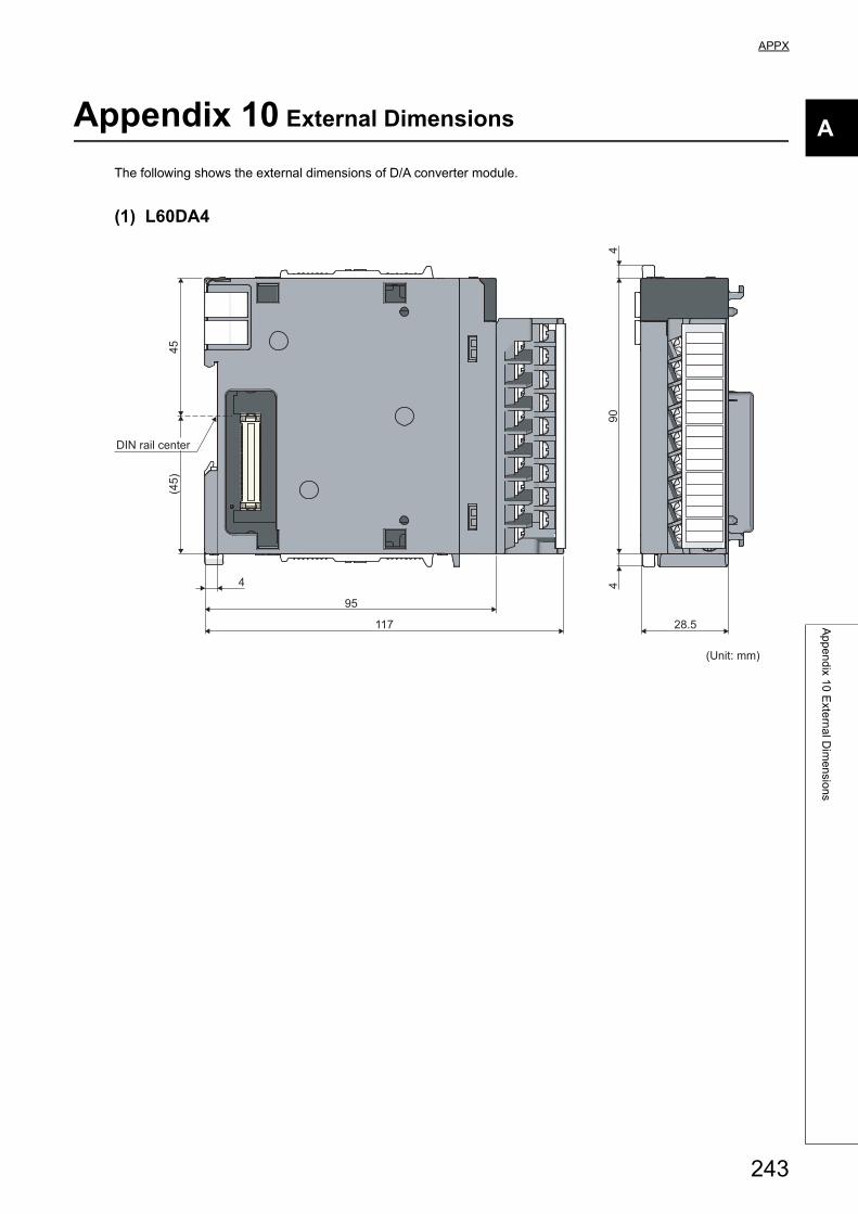
APPX
A
Ap
pe
nd
ix 10
Exte
rna
l Dim
en
sion
s
Appendix 10 External Dimensions
The following shows the external dimensions of D/A converter module.
(1) L60DA4
28.5117
95
4 490
45(4
5)
4
(Unit: mm)
DIN rail center
243
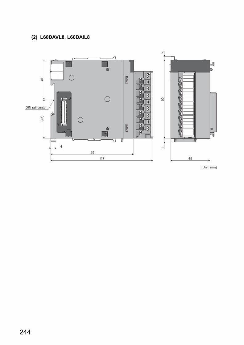
(2) L60DAVL8, L60DAIL8
45117
95
4 490
45(4
5)
4(Unit: mm)
DIN rail center
244
I
4
4
7
8
INDEX
A
Addition of modules. . . . . . . . . . . . . . . . . . . . . . . . 55ALM LED status monitor (Un\G1732) . . . . . . . . . . 213Analog output HOLD/CLEAR function . . . . . . . . . . . 71Analog output test when CPU module is in STOP status. . . . . . . . . . . . . . . . . . . . . . . . . . . . . . . . . . . . . . 75Auto refresh . . . . . . . . . . . . . . . . . . . . . . . . . . . . . 59
C
CH1 Industrial shipment settings offset value (Un\G202) to CH4 User range settings gain value (Un\G217). . . . . . . . . . . . . . . . . . . . . . . . . . . . . . . . . . . . . 199CH1 Industrial shipment settings offset value (Un\G202) to CH8 User range settings gain value (Un\G233). . . . . . . . . . . . . . . . . . . . . . . . . . . . . . . . . . . . . 199CH1 Scaling lower limit value (Un\G54) to CH8 Scaling upper limit value (Un\G69) . . . . . . . . . . . . . . . . . . 196CH1 to CH8 Analog output command value (Un\G1710, Un\G1712, Un\G1714, Un\G1716, Un\G1718, Un\G1720, Un\G1722, Un\G1724) . . . . . . . . . . . . 212CH1 to CH8 Analog output command value unit (Un\G1711, Un\G1713, Un\G1715, Un\G1717, Un\G1719, Un\G1721, Un\G1723, Un\G1725) . . . . 213CH1 to CH8 Constant for wave output conversion cycle (Un\G1064 to Un\G1071) . . . . . . . . . . . . . . . . . . . 204CH1 to CH8 D/A conversion status (Un\G1700 to Un\G1707) . . . . . . . . . . . . . . . . . . . . . . . . . . . . . 212CH1 to CH8 Digital value (Un\G1 to Un\G8) . . . . . . 190CH1 to CH8 Output enable/disable flag (Y1 to Y8). . . . . . . . . . . . . . . . . . . . . . . . . . . . . . . . . . . . . 188CH1 to CH8 Output setting during wave output stop (Un\G1008 to Un\G1015) . . . . . . . . . . . . . . . . . . . 200CH1 to CH8 Output value during wave output stop (Un\G1016 to Un\G1023) . . . . . . . . . . . . . . . . . . . 201CH1 to CH8 Set value check code (Un\G11 to Un\G18). . . . . . . . . . . . . . . . . . . . . . . . . . . . . . . . . . . . . 191CH1 to CH8 Wave output current digital value monitor (Un\G1148 to Un\G1155) . . . . . . . . . . . . . . . . . . . 209CH1 to CH8 Wave output start/stop request (Un\G1000 to Un\G1007) . . . . . . . . . . . . . . . . . . . . . . . . . . . 200CH1 to CH8 Wave output status monitor (Un\G1100 to Un\G1107) . . . . . . . . . . . . . . . . . . . . . . . . . . . . . 207CH1 to CH8 Wave output step action movement amount (Un\G1080 to Un\G1087) . . . . . . . . . . . . . . . . . . . 206CH1 to CH8 Wave pattern output count monitor (Un\G1124 to Un\G1131) . . . . . . . . . . . . . . . . . . . 207CH1 to CH8 Wave pattern output repetition setting (Un\G1056 to Un\G1063) . . . . . . . . . . . . . . . . . . . 204CH1 Warning output upper limit value (Un\G86) to CH8 Warning output lower limit value (Un\G101) . . . . . . 197CH1 Wave output conversion cycle monitor (L) (Un\G1108) to CH8 Wave output conversion cycle monitor (H) (Un\G1123) . . . . . . . . . . . . . . . . . . . . 207CH1 Wave output current address monitor (L) (Un\G1132) to CH8 Wave output current address monitor (H) (Un\G1147). . . . . . . . . . . . . . . . . . . . . . . . . . 208
CH1 Wave output digital value outside the range Address monitor (L) (Un\G1156) to CH8 Wave output digital value outside the range Address monitor (H) (Un\G1171). . . . . . . . . . . . . . . . . . . . . . . . . . . . . . . . . . . . . 210CH1 Wave output warning Address monitor (L) (Un\G1172) to CH8 Wave output warning Address monitor (H) (Un\G1187). . . . . . . . . . . . . . . . . . . . 211CH1 Wave pattern data points setting (L) (Un\G1040) to CH8 Wave pattern data points setting (H) (Un\G1055). . . . . . . . . . . . . . . . . . . . . . . . . . . . . . . . . . . . . 203CH1 Wave pattern start address setting (L) (Un\G1024) to CH8 Wave pattern start address setting (H) (Un\G1039) . . . . . . . . . . . . . . . . . . . . . . . . . . . . 202Channel change completed flag (XB) . . . . . . . . . . 185Channel change request (YB) . . . . . . . . . . . . . . . 189Current output characteristic . . . . . . . . . . . . . . . . 218
D
D/A conversion enable/disable function. . . . . . . . . . 70D/A conversion enable/disable setting (Un\G0) . . . 190D/A output enable/disable function . . . . . . . . . . . . . 70
E
ERR LED status monitor (Un\G1731) . . . . . . . . . . 213Error clear function . . . . . . . . . . . . . . . . . . . . . . . 139Error clear request (YF). . . . . . . . . . . . . . . . . . . . 189Error flag (XF) . . . . . . . . . . . . . . . . . . . . . . . . . . 187Error history clear setting (Un\G1802) . . . . . . . . . . 214Error history No.1 to No.16 (Un\G1810 to Un\G1969). . . . . . . . . . . . . . . . . . . . . . . . . . . . . . . . . . . . . 214Error log function . . . . . . . . . . . . . . . . . . . . . . . . 135External dimensions . . . . . . . . . . . . . . . . . . . . . . 243External power supply READY flag (X7) . . . . . . . . 183External wiring . . . . . . . . . . . . . . . . . . . . . . . . . . . 52
F
For current output . . . . . . . . . . . . . . . . . . . . . . . . . 53For voltage output. . . . . . . . . . . . . . . . . . . . . . . . . 52
G
Gain value . . . . . . . . . . . . . . . . . . . . . . . . . . . . . 216
H
Hardware LED information. . . . . . . . . . . . . . . . . . 182Hardware switch information . . . . . . . . . . . . . . . . 182HOLD/CLEAR function setting (Un\G26, Un\G27). . . . . . . . . . . . . . . . . . . . . . . . . . . . . . . . . . . . . 194
I
I/O assignment . . . . . . . . . . . . . . . . . . . . . . . . . . 237Intelligent function module switch setting. . . . . . . . 238
245
L
Latest address of error history (Un\G1800) . . . . . . 214Latest error code (Un\G19) . . . . . . . . . . . . . . . . . 192
M
Mode switching setting (Un\G158, Un\G159). . . . . 198Module error collection function . . . . . . . . . . . . . . 138Module READY (X0) . . . . . . . . . . . . . . . . . . . . . 183
N
Normal mode. . . . . . . . . . . . . . . . . . . . . . . . . . . . 67Normal output mode. . . . . . . . . . . . . . . . . . . . . . . 67
O
Offset value. . . . . . . . . . . . . . . . . . . . . . . . . . . . 216Offset/gain adjustment value specification (Un\G24) . . . . . . . . . . . . . . . . . . . . . . . . . . . . . . . . . . . . 193Offset/gain setting . . . . . . . . . . . . . . . . . . . . . . . . 60Offset/gain setting mode flag (XA) . . . . . . . . . . . . 185Offset/gain setting mode Gain specification (Un\G23) . . . . . . . . . . . . . . . . . . . . . . . . . . . . . . . . . . . . 193Offset/gain setting mode Offset specification (Un\G22) . . . . . . . . . . . . . . . . . . . . . . . . . . . . . . . . . . . . 193Operating condition setting completed flag (X9). . . 184Operating condition setting request (Y9) . . . . . . . . 188Output mode (Un\G9) . . . . . . . . . . . . . . . . . . . . . 191
P
Parameter setting. . . . . . . . . . . . . . . . . . . . . . . . . 58Pass data classification setting (Un\G200) . . . . . . 198
R
Range reference tables . . . . . . . . . . . . . . . . . . . 145Restrictions and precautions on the wave output function . . . . . . . . . . . . . . . . . . . . . . . . . . . . . . . . . . . . . 90RUN LED status monitor (Un\G1730) . . . . . . . . . . 213
S
Save/restoration of offset/gain value . . . . . . . . . . 140Scaling enable/disable setting (Un\G53) . . . . . . . . 195Scaling function . . . . . . . . . . . . . . . . . . . . . . . . . . 77Set value change completed flag (XC) . . . . . . . . . 186Set value change request (YC) . . . . . . . . . . . . . . 189Setting range (Un\G20, Un\G21) . . . . . . . . . . . . . 192Step action wave output request (Un\G1072) . . . . 205Switch 1 . . . . . . . . . . . . . . . . . . . . . . . . . . . 238,239Switch 2 . . . . . . . . . . . . . . . . . . . . . . . . . . . 238,239Switch 3 . . . . . . . . . . . . . . . . . . . . . . . . . . . 238,239Switch 4 . . . . . . . . . . . . . . . . . . . . . . . . . . . 238,239Switch 5 . . . . . . . . . . . . . . . . . . . . . . . . . . . 238,239Switch setting . . . . . . . . . . . . . . . . . . . . . . . . . . . 56
U
User range writing request (YA). . . . . . . . . . . . . . 188
V
Voltage output characteristic . . . . . . . . . . . . . . . . 217
W
Warning output clear request (YE). . . . . . . . . . . . 189Warning output flag (Un\G48) . . . . . . . . . . . . . . . 195Warning output function . . . . . . . . . . . . . . . . . . . . 83Warning output setting (Un\G47) . . . . . . . . . . . . . 194Warning output signal (XE) . . . . . . . . . . . . . . . . . 186Wave data . . . . . . . . . . . . . . . . . . . . . . . . . . . . . 91Wave data registry area (Un\G5000 to Un\G54999) . . . . . . . . . . . . . . . . . . . . . . . . . . . . . . . . . . . . 215Wave output function . . . . . . . . . . . . . . . . . . . . . . 86Wave output mode. . . . . . . . . . . . . . . . . . . . . . . . 67Wave output step action function. . . . . . . . . . . . . 126Wave pattern . . . . . . . . . . . . . . . . . . . . . . . . . . . 91
246

I
4
4
7
8
247
Memo
248
INSTRUCTION INDEX
G
G(P).OFFGAN. . . . . . . . . . . . . . . . . . . . . . . . . . 223G(P).OGLOAD. . . . . . . . . . . . . . . . . . . . . . . . . . 225G(P).OGSTOR . . . . . . . . . . . . . . . . . . . . . . . . . 229
I
4
4
7
8
249
Memo
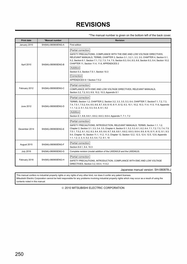
250
REVISIONS
*The manual number is given on the bottom left of the back cover.
Japanese manual version: SH-080878-J
2010 MITSUBISHI ELECTRIC CORPORATION
Print date *Manual number Revision
January 2010 SH(NA)-080900ENG-A First edition
April 2010 SH(NA)-080900ENG-B
SAFETY PRECAUTIONS, COMPLIANCE WITH THE EMC AND LOW VOLTAGE DIRECTIVES,
RELEVANT MANUALS, TERMS, CHAPTER 3, Section 3.1, 3.2.1, 3.3, 3.5, CHAPTER 4, Section 5.1,
5.2, Section 6.1, Section 7.1, 7.2, 7.3, 7.4, 7.5, Section 8.3, 8.4, 8.5, 8.6, Section 9.3, 9.4, Section 10.2,
CHAPTER 11, Section 11.4, 11.6, APPENDICES 2
Section 5.3, Section 7.5.1, Section 10.3
APPENDICES 8.1 Section 7.5.2
February 2012 SH(NA)-080900ENG-C COMPLIANCE WITH EMC AND LOW VOLTAGE DIRECTIVES, RELEVANT MANUALS,
Section 3.2, 7.2, 8.3, 8.9, 10.2, 10.3, Appendix 8.1
June 2012 SH(NA)-080900ENG-D
TERMS, Section 1.2, CHAPTER 2, Section 3.2, 3.3, 3.5, 5.3, 6.4, CHAPTER 7, Section7.1, 7.2, 7.3,
7.4, 7.5.1, 7.5.2, 8.4, 8.5, 8.6, 8.7, 8.9, 8.10, 8.11, 8.12, 9.3, 10.1, 10.2, 10.3, 11.4, 11.5, 11.6, Appendix
1.1, 1.2, 2, 5.1, 5.2, 5.3, 5.4, 8, 9.1, 9.2
Section 8.1, 8.8, 8.8.1, 8.8.2, 8.8.3, 8.8.4, Appendix 7, 7.1, 7.2
December 2014 SH(NA)-080900ENG-E
SAFETY PRECAUTIONS, INTRODUCTION, RELEVANT MANUALS, TERMS, Section 1.1, 1.2,
Chapter 2, Section 3.1, 3.3, 3.4, 3.5, Chapter 4, Section 5.1, 5.2, 5.3, 6.1, 6.2, 6.4, 7.1, 7.2, 7.3, 7.4, 7.5,
7.5.1, 7.5.2, 8.1, 8.2, 8.3, 8.4, 8.5, 8.6, 8.7, 8.8, 8.8.1, 8.8.2, 8.8.3, 8.8.4, 8.9, 8.10, 8.11, 8.12, 9.1, 9.3,
9.4, Chapter 10, Section 11.1, 11.2, 11.3, Chapter 12, Section 12.2, 12.3, 12.4, 12.5, 12.6, Appendix
1.1, 1.2, 2, 3, 4, 5.2, 5.3, 5.4, 7.2, 9.1, 10
August 2015 SH(NA)-080900ENG-FSection 8.8.1, 9.4, 10.3
July 2016 SH(NA)-080900ENG-G Complete revision (model addition of the L60DAVL8 and the L60DAIL8)
February 2018 SH(NA)-080900ENG-H SAFETY PRECAUTIONS, INTRODUCTION, COMPLIANCE WITH EMC AND LOW VOLTAGE
DIRECTIVES, Section 3.2, 8.8.4, 11.6.2
This manual confers no industrial property rights or any rights of any other kind, nor does it confer any patent licenses.
Mitsubishi Electric Corporation cannot be held responsible for any problems involving industrial property rights which may occur as a result of using the
contents noted in this manual.
Partial correction
Addition
Correction
Partial correction
Partial correction
Addition
Partial correction
Partial correction
Partial correction
251
WARRANTY
Please confirm the following product warranty details before using this product.
1. Gratis Warranty Term and Gratis Warranty RangeIf any faults or defects (hereinafter "Failure") found to be the responsibility of Mitsubishi occurs during use of the product within the gratis warranty term, the product shall be repaired at no cost via the sales representative or Mitsubishi Service Company.However, if repairs are required onsite at domestic or overseas location, expenses to send an engineer will be solely at the customer's discretion. Mitsubishi shall not be held responsible for any re-commissioning, maintenance, or testing on-site that involves replacement of the failed module.[Gratis Warranty Term]The gratis warranty term of the product shall be for one year after the date of purchase or delivery to a designated place.Note that after manufacture and shipment from Mitsubishi, the maximum distribution period shall be six (6) months, and the longest gratis warranty term after manufacturing shall be eighteen (18) months. The gratis warranty term of repair parts shall not exceed the gratis warranty term before repairs.[Gratis Warranty Range](1) The range shall be limited to normal use within the usage state, usage methods and usage environment, etc., which
follow the conditions and precautions, etc., given in the instruction manual, user's manual and caution labels on the product.
(2) Even within the gratis warranty term, repairs shall be charged for in the following cases.1. Failure occurring from inappropriate storage or handling, carelessness or negligence by the user. Failure caused
by the user's hardware or software design.2. Failure caused by unapproved modifications, etc., to the product by the user.3. When the Mitsubishi product is assembled into a user's device, Failure that could have been avoided if functions
or structures, judged as necessary in the legal safety measures the user's device is subject to or as necessary by industry standards, had been provided.
4. Failure that could have been avoided if consumable parts (battery, backlight, fuse, etc.) designated in the instruction manual had been correctly serviced or replaced.
5. Failure caused by external irresistible forces such as fires or abnormal voltages, and Failure caused by force majeure such as earthquakes, lightning, wind and water damage.
6. Failure caused by reasons unpredictable by scientific technology standards at time of shipment from Mitsubishi.7. Any other failure found not to be the responsibility of Mitsubishi or that admitted not to be so by the user.
2. Onerous repair term after discontinuation of production(1) Mitsubishi shall accept onerous product repairs for seven (7) years after production of the product is discontinued.
Discontinuation of production shall be notified with Mitsubishi Technical Bulletins, etc.(2) Product supply (including repair parts) is not available after production is discontinued.
3. Overseas serviceOverseas, repairs shall be accepted by Mitsubishi's local overseas FA Center. Note that the repair conditions at each FA Center may differ.
4. Exclusion of loss in opportunity and secondary loss from warranty liabilityRegardless of the gratis warranty term, Mitsubishi shall not be liable for compensation to:(1) Damages caused by any cause found not to be the responsibility of Mitsubishi.(2) Loss in opportunity, lost profits incurred to the user by Failures of Mitsubishi products.(3) Special damages and secondary damages whether foreseeable or not, compensation for accidents, and
compensation for damages to products other than Mitsubishi products.(4) Replacement by the user, maintenance of on-site equipment, start-up test run and other tasks.
5. Changes in product specificationsThe specifications given in the catalogs, manuals or technical documents are subject to change without prior notice.
252
TRADEMARKS
Ethernet is a registered trademark of Fuji Xerox Co., Ltd. in Japan.
Microsoft and Windows are either registered trademarks or trademarks of Microsoft Corporation in the United States
and/or other countries.
Unicode is either a registered trademark or a trademark of Unicode, Inc. in the United States and other countries.
The company names, system names and product names mentioned in this manual are either registered trademarks or
trademarks of their respective companies.
In some cases, trademark symbols such as '' or '' are not specified in this manual.
SH(NA)-080900ENG-H


SH(NA)-080900ENG-H(1802)MEE
MODEL: L-D/A-U-E
MODEL CODE: 13JZ43
Specifications subject to change without notice.
When exported from Japan, this manual does not require application to theMinistry of Economy, Trade and Industry for service transaction permission.
HEAD OFFICE : TOKYO BUILDING, 2-7-3 MARUNOUCHI, CHIYODA-KU, TOKYO 100-8310, JAPANNAGOYA WORKS : 1-14 , YADA-MINAMI 5-CHOME , HIGASHI-KU, NAGOYA , JAPAN
Related Documents