MELSEC-L CPU Module User's Manual (Function Explanation, Program Fundamentals) -L02SCPU -L02SCPU-P -L02CPU -L02CPU-P -L06CPU -L06CPU-P -L26CPU -L26CPU-P -L26CPU-BT -L26CPU-PBT

Welcome message from author
This document is posted to help you gain knowledge. Please leave a comment to let me know what you think about it! Share it to your friends and learn new things together.
Transcript

MELSEC-L CPU Module User's Manual(Function Explanation, Program Fundamentals)
-L02SCPU-L02SCPU-P-L02CPU-L02CPU-P-L06CPU-L06CPU-P-L26CPU-L26CPU-P-L26CPU-BT-L26CPU-PBT


SAFETY PRECAUTIONS(Read these precautions before using this product.)
Before using this product, please read this manual and the relevant manuals carefully and pay full attention
to safety to handle the product correctly.
In this manual, the safety precautions are classified into two levels: " WARNING" and " CAUTION".
Under some circumstances, failure to observe the precautions given under " CAUTION" may lead to
serious consequences.
Observe the precautions of both levels because they are important for personal and system safety.
Make sure that the end users read this manual and then keep the manual in a safe place for future
reference.
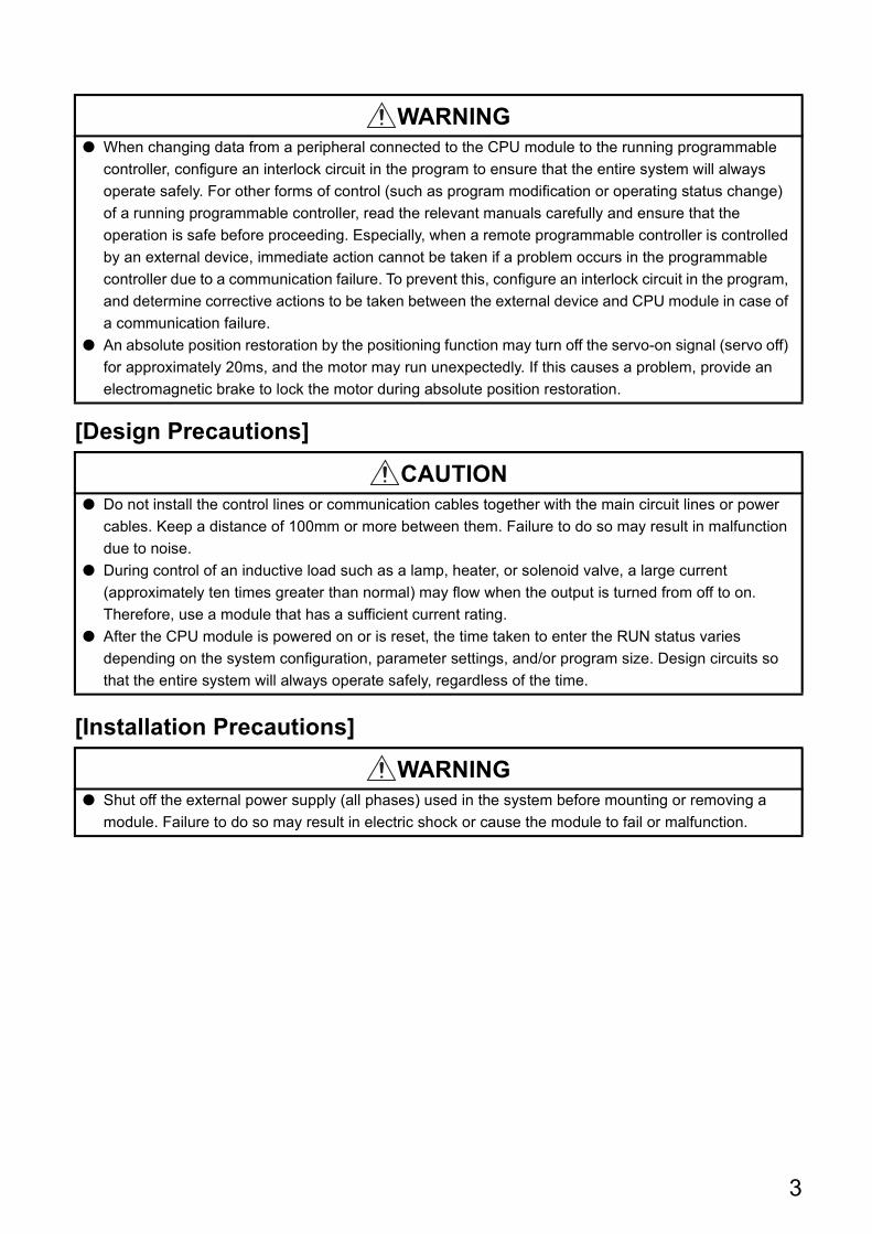
WARNING
CAUTION
Indicates that incorrect handling may cause hazardous conditions,resulting in death or severe injury.
Indicates that incorrect handling may cause hazardous conditions, resulting in minor or moderate injury or property damage.
1

[Design Precautions]
WARNING● Configure safety circuits external to the programmable controller to ensure that the entire system
operates safely even when a fault occurs in the external power supply or the programmable controller.
Failure to do so may result in an accident due to an incorrect output or malfunction.
(1) Emergency stop circuits, protection circuits, and protective interlock circuits for conflicting
operations (such as forward/reverse rotations or upper/lower limit positioning) must be configured
external to the programmable controller.
(2) Machine OPR (Original Point Return) of the positioning function is controlled by two kinds of data:
an OPR direction and an OPR speed. Deceleration starts when the near-point dog signal turns on.
If an incorrect OPR direction is set, motion control may continue without deceleration. To prevent
machine damage caused by this, configure an interlock circuit external to the programmable
controller.
(3) When the CPU module detects an error during control by the positioning function, the motion
slows down and stops.
(4) When the programmable controller detects an abnormal condition, it stops the operation and all
outputs are:
• Turned off if the overcurrent or overvoltage protection of the power supply module is activated.
• Held or turned off according to the parameter setting if the self-diagnostic function of the CPU
module detects an error such as a watchdog timer error.
(5) All outputs may be turned on if an error occurs in a part, such as an I/O control part, where the
CPU module cannot detect any error. To ensure safety operation in such a case, provide a safety
mechanism or a fail-safe circuit external to the programmable controller. For a fail-safe circuit
example, refer to "General Safety Requirements" in the MELSEC-L CPU Module User's Manual
(Hardware Design, Maintenance and Inspection).
(6) Outputs may remain on or off due to a failure of a component such as a transistor in an output
circuit. Configure an external circuit for monitoring output signals that could cause a serious
accident.
● In an output circuit, when a load current exceeding the rated current or an overcurrent caused by a
load short-circuit flows for a long time, it may cause smoke and fire. To prevent this, configure an
external safety circuit, such as a fuse.
● Configure a circuit so that the programmable controller is turned on first and then the external power
supply. If the external power supply is turned on first, an accident may occur due to an incorrect output
or malfunction.
● Configure a circuit so that the external power supply is turned off first and then the programmable
controller. If the programmable controller is turned off first, an accident may occur due to an incorrect
output or malfunction.
● For the operating status of each station after a communication failure, refer to relevant manuals for
each network. Incorrect output or malfunction due to a communication failure may result in an
accident.
2
[Design Precautions]
[Installation Precautions]
● When changing data from a peripheral connected to the CPU module to the running programmable
controller, configure an interlock circuit in the program to ensure that the entire system will always
operate safely. For other forms of control (such as program modification or operating status change)
of a running programmable controller, read the relevant manuals carefully and ensure that the
operation is safe before proceeding. Especially, when a remote programmable controller is controlled
by an external device, immediate action cannot be taken if a problem occurs in the programmable
controller due to a communication failure. To prevent this, configure an interlock circuit in the program,
and determine corrective actions to be taken between the external device and CPU module in case of
a communication failure.
● An absolute position restoration by the positioning function may turn off the servo-on signal (servo off)
for approximately 20ms, and the motor may run unexpectedly. If this causes a problem, provide an
electromagnetic brake to lock the motor during absolute position restoration.
CAUTION● Do not install the control lines or communication cables together with the main circuit lines or power
cables. Keep a distance of 100mm or more between them. Failure to do so may result in malfunction
due to noise.
● During control of an inductive load such as a lamp, heater, or solenoid valve, a large current
(approximately ten times greater than normal) may flow when the output is turned from off to on.
Therefore, use a module that has a sufficient current rating.
● After the CPU module is powered on or is reset, the time taken to enter the RUN status varies
depending on the system configuration, parameter settings, and/or program size. Design circuits so
that the entire system will always operate safely, regardless of the time.
WARNING● Shut off the external power supply (all phases) used in the system before mounting or removing a
module. Failure to do so may result in electric shock or cause the module to fail or malfunction.
WARNING
3

[Installation Precautions]
[Wiring Precautions]
CAUTION● Use the programmable controller in an environment that meets the general specifications in the
MELSEC-L CPU Module User's Manual (Hardware Design, Maintenance and Inspection). Failure to
do so may result in electric shock, fire, malfunction, or damage to or deterioration of the product.
● To interconnect modules, engage the respective connectors and securely lock the module joint levers
until they click. Incorrect interconnection may cause malfunction, failure, or drop of the module.
● Do not directly touch any conductive parts and electronic components of the module. Doing so can
cause malfunction or failure of the module.
● Securely connect an extension cable to the connectors of a branch module and an extension module.
After connections, check that the cable is inserted completely. Poor contact may cause malfunction.
● When using an SD memory card, fully insert it into the SD memory card slot. Check that it is inserted
completely. Poor contact may cause malfunction.
● Do not directly touch any conductive parts and electronic components of the module or SD memory
card. Doing so can cause malfunction or failure of the module.
WARNING● Shut off the external power supply (all phases) used in the system before wiring. Failure to do so may
result in electric shock or cause the module to fail or malfunction.
● After installation and wiring, attach the included terminal cover to the module before turning it on for
operation. Failure to do so may result in electric shock.
4

[Wiring Precautions]
CAUTION● Individually ground the FG terminal of the programmable controller with a ground resistance of 100
or less. Failure to do so may result in electric shock or malfunction.
● Use applicable solderless terminals and tighten them within the specified torque range.
If any spade solderless terminal is used, it may be disconnected when a terminal block screw comes
loose, resulting in failure.
● Check the rated voltage and terminal layout before wiring to the module, and connect the cables
correctly. Connecting a power supply with a different voltage rating or incorrect wiring may cause a fire
or failure.
● Connectors for external devices must be crimped or pressed with the tool specified by the
manufacturer, or must be correctly soldered. Incomplete connections may cause short circuit, fire, or
malfunction.
● Securely connect the connector to the module.
● Do not install the control lines or communication cables together with the main circuit lines or power
cables. Failure to do so may result in malfunction due to noise.
● Place the cables in a duct or clamp them. If not, dangling cable may swing or inadvertently be pulled,
resulting in damage to the module or cables or malfunction due to poor contact.
● Check the interface type and correctly connect the cable. Incorrect wiring (connecting the cable to an
incorrect interface) may cause failure of the module and external device.
● Tighten the terminal block screws within the specified torque range. Undertightening can cause short
circuit, fire, or malfunction. Overtightening can damage the screw and/or module, resulting in drop,
short circuit, fire, or malfunction.
● When disconnecting the cable from the module, do not pull the cable by the cable part. For the cable
with connector, hold the connector part of the cable. For the cable connected to the terminal block,
loosen the terminal screw. Pulling the cable connected to the module may result in malfunction or
damage to the module or cable.
● Prevent foreign matter such as dust or wire chips from entering the module. Such foreign matter can
cause a fire, failure, or malfunction.
● A protective film is attached to the top of the module to prevent foreign matter, such as wire chips,
from entering the module during wiring. Do not remove the film during wiring. Remove it for heat
dissipation before system operation.
● To use the high-speed counter function, ground the shield cable on the encoder side (relay box).
Always ground the FG and LG terminals to the protective ground conductor. Failure to do so may
cause malfunction.
● Mitsubishi programmable controllers must be installed in control panels. Connect the main power
supply to the power supply module in the control panel through a relay terminal block.
Wiring and replacement of a power supply module must be performed by qualified maintenance
personnel with knowledge of protection against electric shock.
For wiring methods, refer to the MELSEC-L CPU Module User's Manual (Hardware Design,
Maintenance and Inspection).
5

[Startup and Maintenance Precautions]
[Startup and Maintenance Precautions]
WARNING● Do not touch any terminal while power is on. Doing so will cause electric shock or malfunction.
● Correctly connect the battery connector. Do not charge, disassemble, heat, short-circuit, solder, or
throw the battery into the fire. Also, do not expose it to liquid or strong shock.
Doing so will cause the battery to produce heat, explode, ignite, or leak, resulting in injury and fire.
● Shut off the external power supply (all phases) used in the system before cleaning the module or
retightening the terminal block screws or connector screws. Failure to do so may result in electric
shock.
CAUTION● Before performing online operations (especially, program modification, forced output, and operating
status change) for the running CPU module from the peripheral connected, read relevant manuals
carefully and ensure the safety. Improper operation may damage machines or cause accidents.
● Do not disassemble or modify the module. Doing so may cause failure, malfunction, injury, or a fire.
● Use any radio communication device such as a cellular phone or PHS (Personal Handy-phone
System) more than 25cm away in all directions from the programmable controller. Failure to do so
may cause malfunction.
● Shut off the external power supply (all phases) used in the system before mounting or removing a
module. Failure to do so may cause the module to fail or malfunction.
● Tighten the terminal block screws or connector screws within the specified torque range.
Undertightening can cause drop of the component or wire, short circuit, or malfunction. Overtightening
can damage the screw and/or module, resulting in drop, short circuit, or malfunction.
● After the first use of the product (module, display unit, and terminal block), do not connect/disconnect
the product more than 50 times (IEC 61131-2/JIS B 3502 compliant). Exceeding the limit may cause
malfunction.
● After the first use of the SD memory card, do not insert/remove the memory card more than 500 times.
Exceeding the limit may cause malfunction.
● Do not drop or apply shock to the battery to be installed in the module. Doing so may damage the
battery, causing the battery fluid to leak inside the battery. If the battery is dropped or any shock is
applied to it, dispose of it without using.
● Before handling the module, touch a conducting object such as a grounded metal to discharge the
static electricity from the human body. Failure to do so may cause the module to fail or malfunction.
● Before testing the operation by the positioning function, set a low speed value for the speed limit
parameter so that the operation can be stopped immediately upon occurrence of a hazardous
condition.
6

[Disposal Precautions]
[Transportation Precautions]
CAUTION● When disposing of this product, treat it as industrial waste. When disposing of batteries, separate
them from other wastes according to the local regulations. (For details on battery regulations in EU
member states, refer to the MELSEC-L CPU Module User's Manual (Hardware Design, Maintenance
and Inspection).)
CAUTION● When transporting lithium batteries, follow the transportation regulations. (For details on the regulated
models, refer to the MELSEC-L CPU Module User's Manual (Hardware Design, Maintenance and
Inspection).)
7

CONDITIONS OF USE FOR THE PRODUCT(1) Mitsubishi programmable controller ("the PRODUCT") shall be used in conditions;
i) where any problem, fault or failure occurring in the PRODUCT, if any, shall not lead to any major or serious accident; and ii) where the backup and fail-safe function are systematically or automatically provided outside of the PRODUCT for the case of any problem, fault or failure occurring in the PRODUCT.
(2) The PRODUCT has been designed and manufactured for the purpose of being used in general industries.MITSUBISHI SHALL HAVE NO RESPONSIBILITY OR LIABILITY (INCLUDING, BUT NOT LIMITED TO ANY AND ALL RESPONSIBILITY OR LIABILITY BASED ON CONTRACT, WARRANTY, TORT, PRODUCT LIABILITY) FOR ANY INJURY OR DEATH TO PERSONS OR LOSS OR DAMAGE TO PROPERTY CAUSED BY the PRODUCT THAT ARE OPERATED OR USED IN APPLICATION NOT INTENDED OR EXCLUDED BY INSTRUCTIONS, PRECAUTIONS, OR WARNING CONTAINED IN MITSUBISHI'S USER, INSTRUCTION AND/OR SAFETY MANUALS, TECHNICAL BULLETINS AND GUIDELINES FOR the PRODUCT. ("Prohibited Application")Prohibited Applications include, but not limited to, the use of the PRODUCT in;• Nuclear Power Plants and any other power plants operated by Power companies, and/or any other cases in which the
public could be affected if any problem or fault occurs in the PRODUCT.• Railway companies or Public service purposes, and/or any other cases in which establishment of a special quality
assurance system is required by the Purchaser or End User.• Aircraft or Aerospace, Medical applications, Train equipment, transport equipment such as Elevator and Escalator,
Incineration and Fuel devices, Vehicles, Manned transportation, Equipment for Recreation and Amusement, and Safety devices, handling of Nuclear or Hazardous Materials or Chemicals, Mining and Drilling, and/or other applications where there is a significant risk of injury to the public or property.
Notwithstanding the above restrictions, Mitsubishi may in its sole discretion, authorize use of the PRODUCT in one or more of the Prohibited Applications, provided that the usage of the PRODUCT is limited only for the specific applications agreed to by Mitsubishi and provided further that no special quality assurance or fail-safe, redundant or other safety features which exceed the general specifications of the PRODUCTs are required. For details, please contact the Mitsubishi representative in your region.
8

INTRODUCTION
Thank you for purchasing the Mitsubishi Electric MELSEC-L series programmable controllers.
This manual describes the memory maps, functions, and devices of the CPU module, and programming.
Before using this product, please read this manual and the relevant manuals carefully and develop familiarity with the
functions and performance of the MELSEC-L series programmable controller to handle the product correctly.
When applying the program examples introduced in this manual to an actual system, ensure the applicability and
confirm that it will not cause system control problems.
Relevant CPU modules
Remark
This manual does not describe the details of the instructions, error codes, special relay (SM), and special register (SD).
● For the instructions, refer to the following.MELSEC-Q/L Programming Manual (Common Instruction)
● For the error codes, special relay(SM), and special register (SD), refer to the following.MELSEC-L CPU Module User's Manual (Hardware Design, Maintenance and Inspection)
CPU module Model
LCPUL02SCPU, L02SCPU-P, L02CPU, L02CPU-P, L06CPU, L06CPU-P, L26CPU, L26CPU-P,
L26CPU-BT, L26CPU-PBT
9

RELEVANT MANUALS
(1) CPU module user's manual
(2) Programming manual
(3) Operating manual
Manual name
<manual number (model code)>Description
MELSEC-L CPU Module User's Manual (Hardware Design, Maintenance and
Inspection)
<SH-080890ENG, 13JZ36>
Specifications of the CPU modules, power supply modules, display unit,
branch module, extension module, SD memory cards, and batteries,
information on how to establish a system, maintenance and inspection, and
troubleshooting
MELSEC-L CPU Module User's Manual (Built-In Ethernet Function)
<SH-080891ENG, 13JZ37>The built-in Ethernet function of the CPU module
MELSEC-L CPU Module User's Manual (Built-In I/O Function)
<SH-080892ENG, 13JZ38>
The general-purpose I/O function, interrupt input function, pulse catch
function, positioning function, and high-speed counter function of the CPU
module
QnUDVCPU/LCPU User's Manual (Data Logging Function)
<SH-080893ENG, 13JZ39>The data logging function of the CPU module
Manual name
<manual number (model code)>Description
MELSEC-Q/L Programming Manual (Common Instruction)
<SH-080809ENG, 13JW10>Detailed description and usage of instructions used in programs
MELSEC-Q/L/QnA Programming Manual (SFC)
<SH-080041, 13JF60>
System configuration, specifications, functions, programming, and error codes
for SFC (MELSAP3) programs
MELSEC-Q/L Programming Manual (MELSAP-L)
<SH-080076, 13JF61>
System configuration, specifications, functions, programming, and error codes
for SFC (MELSAP-L) programs
MELSEC-Q/L Programming Manual (Structured Text)
<SH-080366E, 13JF68>System configuration and programming using structured text language
MELSEC-Q/L/QnA Programming Manual (PID Control Instructions)
<SH-080040, 13JF59>Dedicated instructions for PID control
Manual name
<manual number (model code)>Description
GX Works2 Version 1 Operating Manual (Common)
<SH-080779ENG, 13JU63>
System configuration, parameter settings, and online operations of GX
Works2, which are common to Simple projects and Structured projects
GX Developer Version 8 Operating Manual
<SH-080373E, 13JU41>
Operating methods of GX Developer, such as programming, printing,
monitoring, and debugging
10

(4) I/O module and intelligent function module manual
(5) Others
Manual name
<manual number (model code)>Description
MELSEC-L I/O Module User's Manual
<SH-080888ENG, 13JZ34>Specifications and troubleshooting of the I/O module
MELSEC-L Ethernet Interface Module User's Manual (Basic)
<SH-081105ENG, 13JZ73>
Specifications, procedures for data communication with external devices, line
connection (open/close), fixed buffer communication, random access buffer
communication, and troubleshooting of the Ethernet module
MELSEC-L Serial Communication Module User’s Manual (Basic)
<SH-080894ENG, 13JZ40>
System configuration, specifications, procedures before operation, data
communication methods (basic), and troubleshooting of the serial
communication module
MELSEC Communication Protocol Reference Manual
<SH-080008, 13JF89>
Details of MELSEC communication protocol (MC protocol) that is used for
data communication between a target device and a CPU module
MELSEC-L CC-Link System Master/Local Module User's Manual
<SH-080895ENG, 13JZ41>
Settings, specifications, handling, data communication methods, and
troubleshooting of the built-in CC-Link function of the CPU module or the CC-
Link system master/local module
MELSEC-L CC-Link/LT Master Module User's Manual
<SH-081012ENG, 13JZ65>
Settings, specifications, handling, data communication methods, and
troubleshooting of the CC-Link/LT master module
MELSEC-L CC-Link IE Field Network Master/Local Module User's Manual
<SH-080972ENG, 13JZ54>
Overview of CC-Link IE Field Network, and specifications, procedures before
operation, system configuration, installation, wiring, settings, functions,
programming, and troubleshooting of the MELSEC-L series CC-Link IE Field
Network master/local module
MELSEC-L Analog-Digital Converter Module User's Manual
<SH-080899ENG, 13JZ42>
System configuration, specifications, settings, and troubleshooting of the
analog-digital converter module
MELSEC-L Dual Channel Isolated High Resolution Analog-Digital Converter
Module User's Manual
<SH-081103ENG, 13JZ72>
System configuration, specifications, settings, and troubleshooting of the dual
channel isolated high resolution analog-digital converter module
MELSEC-L Digital-Analog Converter Module User's Manual
<SH-080900ENG, 13JZ43>
System configuration, specifications, settings, and troubleshooting of the
digital-analog converter module
MELSEC-L Analog Input/Output Module User's Manual
<SH-081167ENG, 13JZ87>
System configuration, specifications, settings, and troubleshooting of the
analog input/output module
MELSEC-L LD75P/LD75D Positioning Module User's Manual
<SH-080911ENG, 13JZ46>
System configuration specifications settings and troubleshooting of the
positioning module
MELSEC-L High-Speed Counter Module User's Manual
<SH-080920ENG, 13JZ49>
System configuration specifications settings and troubleshooting of the high-
speed counter module
MELSEC-L Temperature Control Module User's Manual
<SH-081000ENG, 13JZ64>
System configuration specifications settings and troubleshooting of the
temperature control module
MELSEC-L Multiple Input (Voltage/Current/Temperature) Module User's
Manual
<SH-081365ENG, 13JZ76>
System configuration, specifications, settings, and troubleshooting of the
multiple input module
Manual name
<manual number (model code)>Description
iQ Sensor Solution Reference Manual
<SH-081133ENG, 13JV28>
Operating methods of iQ Sensor Solution, such as programming and
monitoring
CC-Link IE Field Network Basic Reference Manual
<SH-081684ENG, 13JX62>
Specifications, procedures before operation, system configuration,
programming, functions, parameter settings, and troubleshooting of CC-Link
IE Field Network Basic
11

CONTENTS
12
CONTENTS
SAFETY PRECAUTIONS . . . . . . . . . . . . . . . . . . . . . . . . . . . . . . . . . . . . . . . . . . . . . . . . . . . . . . . . . . . . . 1CONDITIONS OF USE FOR THE PRODUCT . . . . . . . . . . . . . . . . . . . . . . . . . . . . . . . . . . . . . . . . . . . . . 8
INTRODUCTION . . . . . . . . . . . . . . . . . . . . . . . . . . . . . . . . . . . . . . . . . . . . . . . . . . . . . . . . . . . . . . . . . . . . 9RELEVANT MANUALS . . . . . . . . . . . . . . . . . . . . . . . . . . . . . . . . . . . . . . . . . . . . . . . . . . . . . . . . . . . . . . 10MANUAL PAGE ORGANIZATION . . . . . . . . . . . . . . . . . . . . . . . . . . . . . . . . . . . . . . . . . . . . . . . . . . . . . . 17TERMS . . . . . . . . . . . . . . . . . . . . . . . . . . . . . . . . . . . . . . . . . . . . . . . . . . . . . . . . . . . . . . . . . . . . . . . . . . 18GENERIC TERMS AND ABBREVIATIONS. . . . . . . . . . . . . . . . . . . . . . . . . . . . . . . . . . . . . . . . . . . . . . . 18
PART 1 PROGRAMMING
CHAPTER 1 BASIC PROCEDURE FOR PROGRAMMING 20
1.1 System Configuration Example . . . . . . . . . . . . . . . . . . . . . . . . . . . . . . . . . . . . . . . . . . . . . . . . 21
1.2 Creating a Project . . . . . . . . . . . . . . . . . . . . . . . . . . . . . . . . . . . . . . . . . . . . . . . . . . . . . . . . . . . 22
1.3 Creating a Program . . . . . . . . . . . . . . . . . . . . . . . . . . . . . . . . . . . . . . . . . . . . . . . . . . . . . . . . . 23
1.3.1 Prior knowledge for creating a program . . . . . . . . . . . . . . . . . . . . . . . . . . . . . . . . . . . . . . . . . .23
1.3.2 How to create a program . . . . . . . . . . . . . . . . . . . . . . . . . . . . . . . . . . . . . . . . . . . . . . . . . . . . .24
1.4 Converting a Program. . . . . . . . . . . . . . . . . . . . . . . . . . . . . . . . . . . . . . . . . . . . . . . . . . . . . . . . 25
1.5 Writing a Project to the CPU Module . . . . . . . . . . . . . . . . . . . . . . . . . . . . . . . . . . . . . . . . . . . . 26
1.5.1 Formatting a memory . . . . . . . . . . . . . . . . . . . . . . . . . . . . . . . . . . . . . . . . . . . . . . . . . . . . . . . .26
1.5.2 Writing to the CPU module. . . . . . . . . . . . . . . . . . . . . . . . . . . . . . . . . . . . . . . . . . . . . . . . . . . .27
1.6 Checking an Operation of the CPU Module . . . . . . . . . . . . . . . . . . . . . . . . . . . . . . . . . . . . . . . 28
1.7 Saving a Project . . . . . . . . . . . . . . . . . . . . . . . . . . . . . . . . . . . . . . . . . . . . . . . . . . . . . . . . . . . . 30
CHAPTER 2 APPLICATION OF PROGRAMMING 31
2.1 Memory and Files . . . . . . . . . . . . . . . . . . . . . . . . . . . . . . . . . . . . . . . . . . . . . . . . . . . . . . . . . . . 31
2.1.1 Memory configuration. . . . . . . . . . . . . . . . . . . . . . . . . . . . . . . . . . . . . . . . . . . . . . . . . . . . . . . .31
2.1.2 Parameter-valid drive . . . . . . . . . . . . . . . . . . . . . . . . . . . . . . . . . . . . . . . . . . . . . . . . . . . . . . . .34
2.1.3 Files . . . . . . . . . . . . . . . . . . . . . . . . . . . . . . . . . . . . . . . . . . . . . . . . . . . . . . . . . . . . . . . . . . . . .35
2.2 I/O Number . . . . . . . . . . . . . . . . . . . . . . . . . . . . . . . . . . . . . . . . . . . . . . . . . . . . . . . . . . . . . . . . 41
2.2.1 Concept of I/O number assignment . . . . . . . . . . . . . . . . . . . . . . . . . . . . . . . . . . . . . . . . . . . . .41
2.2.2 I/O number assignment . . . . . . . . . . . . . . . . . . . . . . . . . . . . . . . . . . . . . . . . . . . . . . . . . . . . . .43
2.3 Scan Time Structure . . . . . . . . . . . . . . . . . . . . . . . . . . . . . . . . . . . . . . . . . . . . . . . . . . . . . . . . . 45
2.3.1 Initial processing . . . . . . . . . . . . . . . . . . . . . . . . . . . . . . . . . . . . . . . . . . . . . . . . . . . . . . . . . . .45
2.3.2 Refresh processing of input/output modules or intelligent function modules . . . . . . . . . . . . . .46
2.3.3 Program operation . . . . . . . . . . . . . . . . . . . . . . . . . . . . . . . . . . . . . . . . . . . . . . . . . . . . . . . . . .46
2.3.4 END processing . . . . . . . . . . . . . . . . . . . . . . . . . . . . . . . . . . . . . . . . . . . . . . . . . . . . . . . . . . . .47
2.4 Operation Processing of the CPU Module for Each Operating Status . . . . . . . . . . . . . . . . . . . 48
2.5 Operation Processing During Momentary Power Failure . . . . . . . . . . . . . . . . . . . . . . . . . . . . . 50
2.6 Processing of Inputs and Outputs. . . . . . . . . . . . . . . . . . . . . . . . . . . . . . . . . . . . . . . . . . . . . . . 51
2.6.1 Refresh processing . . . . . . . . . . . . . . . . . . . . . . . . . . . . . . . . . . . . . . . . . . . . . . . . . . . . . . . . .51
2.6.2 Direct processing . . . . . . . . . . . . . . . . . . . . . . . . . . . . . . . . . . . . . . . . . . . . . . . . . . . . . . . . . . .54
2.7 Interrupt Program . . . . . . . . . . . . . . . . . . . . . . . . . . . . . . . . . . . . . . . . . . . . . . . . . . . . . . . . . . . 56
2.8 Executing Multiple Programs . . . . . . . . . . . . . . . . . . . . . . . . . . . . . . . . . . . . . . . . . . . . . . . . . . 61
2.8.1 Initial execution type program . . . . . . . . . . . . . . . . . . . . . . . . . . . . . . . . . . . . . . . . . . . . . . . . .63
2.8.2 Scan execution type program . . . . . . . . . . . . . . . . . . . . . . . . . . . . . . . . . . . . . . . . . . . . . . . . .65

2.8.3 Standby type program . . . . . . . . . . . . . . . . . . . . . . . . . . . . . . . . . . . . . . . . . . . . . . . . . . . . . . .66
2.8.4 Fixed scan execution type program . . . . . . . . . . . . . . . . . . . . . . . . . . . . . . . . . . . . . . . . . . . . .69
2.8.5 Changing the program execution type . . . . . . . . . . . . . . . . . . . . . . . . . . . . . . . . . . . . . . . . . . .72
2.9 Boot Operation . . . . . . . . . . . . . . . . . . . . . . . . . . . . . . . . . . . . . . . . . . . . . . . . . . . . . . . . . . . . . 74
2.10 Programming Language . . . . . . . . . . . . . . . . . . . . . . . . . . . . . . . . . . . . . . . . . . . . . . . . . . . . . . 76
2.11 Communications with Intelligent Function Modules . . . . . . . . . . . . . . . . . . . . . . . . . . . . . . . . . 77
PART 2 FUNCTIONS
CHAPTER 3 CPU MODULE FUNCTIONS 82
3.1 Function List . . . . . . . . . . . . . . . . . . . . . . . . . . . . . . . . . . . . . . . . . . . . . . . . . . . . . . . . . . . . . . . 82
3.2 Constant Scan . . . . . . . . . . . . . . . . . . . . . . . . . . . . . . . . . . . . . . . . . . . . . . . . . . . . . . . . . . . . . 85
3.3 Watchdog Timer (WDT) . . . . . . . . . . . . . . . . . . . . . . . . . . . . . . . . . . . . . . . . . . . . . . . . . . . . . . 87
3.4 Latch Function . . . . . . . . . . . . . . . . . . . . . . . . . . . . . . . . . . . . . . . . . . . . . . . . . . . . . . . . . . . . . 88
3.5 Initial Device Value . . . . . . . . . . . . . . . . . . . . . . . . . . . . . . . . . . . . . . . . . . . . . . . . . . . . . . . . . . 91
3.6 Service Processing Setting. . . . . . . . . . . . . . . . . . . . . . . . . . . . . . . . . . . . . . . . . . . . . . . . . . . . 94
3.7 Output Mode at Operating Status Change (STOP to RUN) . . . . . . . . . . . . . . . . . . . . . . . . . . 101
3.8 Input Response Time Setting . . . . . . . . . . . . . . . . . . . . . . . . . . . . . . . . . . . . . . . . . . . . . . . . . 102
3.9 Error Time Output Mode Setting . . . . . . . . . . . . . . . . . . . . . . . . . . . . . . . . . . . . . . . . . . . . . . . 103
3.10 PLC Operation Mode at H/W Error Setting. . . . . . . . . . . . . . . . . . . . . . . . . . . . . . . . . . . . . . . 104
3.11 Security Function . . . . . . . . . . . . . . . . . . . . . . . . . . . . . . . . . . . . . . . . . . . . . . . . . . . . . . . . . . 105
3.11.1 File Password 32 . . . . . . . . . . . . . . . . . . . . . . . . . . . . . . . . . . . . . . . . . . . . . . . . . . . . . . . . . .105
3.11.2 Remote Password . . . . . . . . . . . . . . . . . . . . . . . . . . . . . . . . . . . . . . . . . . . . . . . . . . . . . . . . .110
3.12 Remote Operation . . . . . . . . . . . . . . . . . . . . . . . . . . . . . . . . . . . . . . . . . . . . . . . . . . . . . . . . . 112
3.12.1 Remote RUN/STOP . . . . . . . . . . . . . . . . . . . . . . . . . . . . . . . . . . . . . . . . . . . . . . . . . . . . . . . .112
3.12.2 Remote PAUSE . . . . . . . . . . . . . . . . . . . . . . . . . . . . . . . . . . . . . . . . . . . . . . . . . . . . . . . . . . . 114
3.12.3 Remote RESET . . . . . . . . . . . . . . . . . . . . . . . . . . . . . . . . . . . . . . . . . . . . . . . . . . . . . . . . . . . 116
3.12.4 Remote Latch Clear . . . . . . . . . . . . . . . . . . . . . . . . . . . . . . . . . . . . . . . . . . . . . . . . . . . . . . . .117
3.13 Scan Time Measurement . . . . . . . . . . . . . . . . . . . . . . . . . . . . . . . . . . . . . . . . . . . . . . . . . . . . 118
3.14 Program List Monitor . . . . . . . . . . . . . . . . . . . . . . . . . . . . . . . . . . . . . . . . . . . . . . . . . . . . . . . 121
3.15 Interrupt Program List Monitor . . . . . . . . . . . . . . . . . . . . . . . . . . . . . . . . . . . . . . . . . . . . . . . . 122
3.16 Monitor condition setting. . . . . . . . . . . . . . . . . . . . . . . . . . . . . . . . . . . . . . . . . . . . . . . . . . . . . 123
3.17 Local Device Monitor/Test. . . . . . . . . . . . . . . . . . . . . . . . . . . . . . . . . . . . . . . . . . . . . . . . . . . . 128
3.18 External Input/Output Forced On/Off . . . . . . . . . . . . . . . . . . . . . . . . . . . . . . . . . . . . . . . . . . . 131
3.19 Executional Conditioned Device Test . . . . . . . . . . . . . . . . . . . . . . . . . . . . . . . . . . . . . . . . . . . 135
3.20 Sampling Trace. . . . . . . . . . . . . . . . . . . . . . . . . . . . . . . . . . . . . . . . . . . . . . . . . . . . . . . . . . . . 143
3.21 Realtime Monitor Function . . . . . . . . . . . . . . . . . . . . . . . . . . . . . . . . . . . . . . . . . . . . . . . . . . . 150
3.22 Writing Programs in RUN Status . . . . . . . . . . . . . . . . . . . . . . . . . . . . . . . . . . . . . . . . . . . . . . 151
3.22.1 Online change (ladder mode). . . . . . . . . . . . . . . . . . . . . . . . . . . . . . . . . . . . . . . . . . . . . . . . .151
3.22.2 Online change (files) . . . . . . . . . . . . . . . . . . . . . . . . . . . . . . . . . . . . . . . . . . . . . . . . . . . . . . .152
3.22.3 Precautions for online change . . . . . . . . . . . . . . . . . . . . . . . . . . . . . . . . . . . . . . . . . . . . . . . .153
3.23 Debug from Multiple Programming Tools . . . . . . . . . . . . . . . . . . . . . . . . . . . . . . . . . . . . . . . . 158
3.23.1 Simultaneous monitoring from multiple programming tools . . . . . . . . . . . . . . . . . . . . . . . . . .159
3.23.2 Online change from multiple programming tools . . . . . . . . . . . . . . . . . . . . . . . . . . . . . . . . . .160
13

14
3.24 Self-Diagnostic Function. . . . . . . . . . . . . . . . . . . . . . . . . . . . . . . . . . . . . . . . . . . . . . . . . . . . . 161
3.25 Error Clear . . . . . . . . . . . . . . . . . . . . . . . . . . . . . . . . . . . . . . . . . . . . . . . . . . . . . . . . . . . . . . . 166
3.26 LED Control Function . . . . . . . . . . . . . . . . . . . . . . . . . . . . . . . . . . . . . . . . . . . . . . . . . . . . . . . 169
3.26.1 Methods for turning off the LEDs . . . . . . . . . . . . . . . . . . . . . . . . . . . . . . . . . . . . . . . . . . . . . .169
3.26.2 LED indication priority . . . . . . . . . . . . . . . . . . . . . . . . . . . . . . . . . . . . . . . . . . . . . . . . . . . . . .170
3.27 Module Error Collection Function . . . . . . . . . . . . . . . . . . . . . . . . . . . . . . . . . . . . . . . . . . . . . . 171
3.28 Latch Data Backup to Standard ROM . . . . . . . . . . . . . . . . . . . . . . . . . . . . . . . . . . . . . . . . . . 175
3.28.1 Latch data backup . . . . . . . . . . . . . . . . . . . . . . . . . . . . . . . . . . . . . . . . . . . . . . . . . . . . . . . . .176
3.28.2 Restoring backup data . . . . . . . . . . . . . . . . . . . . . . . . . . . . . . . . . . . . . . . . . . . . . . . . . . . . . .179
3.29 Writing/Reading Device Data to/from Standard ROM . . . . . . . . . . . . . . . . . . . . . . . . . . . . . . 180
3.30 Module Model Name Read . . . . . . . . . . . . . . . . . . . . . . . . . . . . . . . . . . . . . . . . . . . . . . . . . . . 181
3.31 CPU Module Change Function with SD Memory Card. . . . . . . . . . . . . . . . . . . . . . . . . . . . . . 182
3.31.1 Backup to SD memory card . . . . . . . . . . . . . . . . . . . . . . . . . . . . . . . . . . . . . . . . . . . . . . . . . .184
3.31.2 Backup data restoration . . . . . . . . . . . . . . . . . . . . . . . . . . . . . . . . . . . . . . . . . . . . . . . . . . . . .192
3.32 Clock Function . . . . . . . . . . . . . . . . . . . . . . . . . . . . . . . . . . . . . . . . . . . . . . . . . . . . . . . . . . . . 196
3.33 Battery Life-Prolonging Function . . . . . . . . . . . . . . . . . . . . . . . . . . . . . . . . . . . . . . . . . . . . . . 198
3.34 Memory Check Function. . . . . . . . . . . . . . . . . . . . . . . . . . . . . . . . . . . . . . . . . . . . . . . . . . . . . 199
3.35 Program Cache Memory Auto Recovery Function . . . . . . . . . . . . . . . . . . . . . . . . . . . . . . . . . 200
3.36 Project Data Batch Save/Load Function. . . . . . . . . . . . . . . . . . . . . . . . . . . . . . . . . . . . . . . . . 202
3.36.1 Batch save . . . . . . . . . . . . . . . . . . . . . . . . . . . . . . . . . . . . . . . . . . . . . . . . . . . . . . . . . . . . . . .203
3.36.2 Batch load . . . . . . . . . . . . . . . . . . . . . . . . . . . . . . . . . . . . . . . . . . . . . . . . . . . . . . . . . . . . . . .209
3.37 Predefined Protocol Function . . . . . . . . . . . . . . . . . . . . . . . . . . . . . . . . . . . . . . . . . . . . . . . . . 215
3.37.1 Communications via Ethernet . . . . . . . . . . . . . . . . . . . . . . . . . . . . . . . . . . . . . . . . . . . . . . . .215
3.37.2 Communications via RS-232 and RS-422/485 . . . . . . . . . . . . . . . . . . . . . . . . . . . . . . . . . . .216
3.38 Serial Communication Function . . . . . . . . . . . . . . . . . . . . . . . . . . . . . . . . . . . . . . . . . . . . . . . 227
3.39 iQ Sensor Solution Function. . . . . . . . . . . . . . . . . . . . . . . . . . . . . . . . . . . . . . . . . . . . . . . . . . 234
CHAPTER 4 DISPLAY UNIT FUNCTIONS 236
4.1 Function List . . . . . . . . . . . . . . . . . . . . . . . . . . . . . . . . . . . . . . . . . . . . . . . . . . . . . . . . . . . . . . 240
4.2 CPU Monitor/Test . . . . . . . . . . . . . . . . . . . . . . . . . . . . . . . . . . . . . . . . . . . . . . . . . . . . . . . . . . 241
4.2.1 Device monitor/test . . . . . . . . . . . . . . . . . . . . . . . . . . . . . . . . . . . . . . . . . . . . . . . . . . . . . . . .241
4.2.2 Device clear . . . . . . . . . . . . . . . . . . . . . . . . . . . . . . . . . . . . . . . . . . . . . . . . . . . . . . . . . . . . . .249
4.2.3 Forced on/off . . . . . . . . . . . . . . . . . . . . . . . . . . . . . . . . . . . . . . . . . . . . . . . . . . . . . . . . . . . . .251
4.2.4 Scan time monitor . . . . . . . . . . . . . . . . . . . . . . . . . . . . . . . . . . . . . . . . . . . . . . . . . . . . . . . . .254
4.2.5 Built-in I/O function monitor . . . . . . . . . . . . . . . . . . . . . . . . . . . . . . . . . . . . . . . . . . . . . . . . . .255
4.2.6 Error display/clear . . . . . . . . . . . . . . . . . . . . . . . . . . . . . . . . . . . . . . . . . . . . . . . . . . . . . . . . .259
4.3 CPU Settings . . . . . . . . . . . . . . . . . . . . . . . . . . . . . . . . . . . . . . . . . . . . . . . . . . . . . . . . . . . . . 263
4.3.1 Clock setting. . . . . . . . . . . . . . . . . . . . . . . . . . . . . . . . . . . . . . . . . . . . . . . . . . . . . . . . . . . . . .263
4.4 Module Monitor/Test . . . . . . . . . . . . . . . . . . . . . . . . . . . . . . . . . . . . . . . . . . . . . . . . . . . . . . . . 265
4.4.1 Buffer memory monitor/test . . . . . . . . . . . . . . . . . . . . . . . . . . . . . . . . . . . . . . . . . . . . . . . . . .265
4.5 Module Settings . . . . . . . . . . . . . . . . . . . . . . . . . . . . . . . . . . . . . . . . . . . . . . . . . . . . . . . . . . . 270
4.5.1 Initial setting change . . . . . . . . . . . . . . . . . . . . . . . . . . . . . . . . . . . . . . . . . . . . . . . . . . . . . . .270
4.6 User Message. . . . . . . . . . . . . . . . . . . . . . . . . . . . . . . . . . . . . . . . . . . . . . . . . . . . . . . . . . . . . 273
4.7 Memory Card Operation . . . . . . . . . . . . . . . . . . . . . . . . . . . . . . . . . . . . . . . . . . . . . . . . . . . . . 274
4.7.1 File list/delete . . . . . . . . . . . . . . . . . . . . . . . . . . . . . . . . . . . . . . . . . . . . . . . . . . . . . . . . . . . . .274

4.7.2 Free space display . . . . . . . . . . . . . . . . . . . . . . . . . . . . . . . . . . . . . . . . . . . . . . . . . . . . . . . . .279
4.7.3 Batch save . . . . . . . . . . . . . . . . . . . . . . . . . . . . . . . . . . . . . . . . . . . . . . . . . . . . . . . . . . . . . . .280
4.7.4 Batch load . . . . . . . . . . . . . . . . . . . . . . . . . . . . . . . . . . . . . . . . . . . . . . . . . . . . . . . . . . . . . . .281
4.8 Options . . . . . . . . . . . . . . . . . . . . . . . . . . . . . . . . . . . . . . . . . . . . . . . . . . . . . . . . . . . . . . . . . . 283
4.8.1 Language setting . . . . . . . . . . . . . . . . . . . . . . . . . . . . . . . . . . . . . . . . . . . . . . . . . . . . . . . . . .283
4.8.2 Contrast adjustment . . . . . . . . . . . . . . . . . . . . . . . . . . . . . . . . . . . . . . . . . . . . . . . . . . . . . . . .284
4.8.3 Lighting period setting . . . . . . . . . . . . . . . . . . . . . . . . . . . . . . . . . . . . . . . . . . . . . . . . . . . . . .285
4.8.4 Pop-up display . . . . . . . . . . . . . . . . . . . . . . . . . . . . . . . . . . . . . . . . . . . . . . . . . . . . . . . . . . . .286
PART 3 DEVICES, CONSTANTS
CHAPTER 5 DEVICES 288
5.1 Device List . . . . . . . . . . . . . . . . . . . . . . . . . . . . . . . . . . . . . . . . . . . . . . . . . . . . . . . . . . . . . . . 288
5.2 Internal User Devices . . . . . . . . . . . . . . . . . . . . . . . . . . . . . . . . . . . . . . . . . . . . . . . . . . . . . . . 290
5.2.1 Input (X) . . . . . . . . . . . . . . . . . . . . . . . . . . . . . . . . . . . . . . . . . . . . . . . . . . . . . . . . . . . . . . . . .293
5.2.2 Output (Y). . . . . . . . . . . . . . . . . . . . . . . . . . . . . . . . . . . . . . . . . . . . . . . . . . . . . . . . . . . . . . . .293
5.2.3 Internal relay (M) . . . . . . . . . . . . . . . . . . . . . . . . . . . . . . . . . . . . . . . . . . . . . . . . . . . . . . . . . .294
5.2.4 Latch relay (L) . . . . . . . . . . . . . . . . . . . . . . . . . . . . . . . . . . . . . . . . . . . . . . . . . . . . . . . . . . . .294
5.2.5 Link relay (B) . . . . . . . . . . . . . . . . . . . . . . . . . . . . . . . . . . . . . . . . . . . . . . . . . . . . . . . . . . . . .294
5.2.6 Annunciator (F) . . . . . . . . . . . . . . . . . . . . . . . . . . . . . . . . . . . . . . . . . . . . . . . . . . . . . . . . . . .295
5.2.7 Link special relay (SB) . . . . . . . . . . . . . . . . . . . . . . . . . . . . . . . . . . . . . . . . . . . . . . . . . . . . . .298
5.2.8 Edge relay (V) . . . . . . . . . . . . . . . . . . . . . . . . . . . . . . . . . . . . . . . . . . . . . . . . . . . . . . . . . . . .298
5.2.9 Step relay (S) . . . . . . . . . . . . . . . . . . . . . . . . . . . . . . . . . . . . . . . . . . . . . . . . . . . . . . . . . . . . .299
5.2.10 Timer (T, ST) . . . . . . . . . . . . . . . . . . . . . . . . . . . . . . . . . . . . . . . . . . . . . . . . . . . . . . . . . . . . .299
5.2.11 Counter (C) . . . . . . . . . . . . . . . . . . . . . . . . . . . . . . . . . . . . . . . . . . . . . . . . . . . . . . . . . . . . . .308
5.2.12 Data register (D). . . . . . . . . . . . . . . . . . . . . . . . . . . . . . . . . . . . . . . . . . . . . . . . . . . . . . . . . . .311
5.2.13 Link register (W). . . . . . . . . . . . . . . . . . . . . . . . . . . . . . . . . . . . . . . . . . . . . . . . . . . . . . . . . . .312
5.2.14 Link special register (SW) . . . . . . . . . . . . . . . . . . . . . . . . . . . . . . . . . . . . . . . . . . . . . . . . . . .313
5.3 Internal System Devices . . . . . . . . . . . . . . . . . . . . . . . . . . . . . . . . . . . . . . . . . . . . . . . . . . . . . 314
5.3.1 Function devices (FX, FY, FD) . . . . . . . . . . . . . . . . . . . . . . . . . . . . . . . . . . . . . . . . . . . . . . . .314
5.3.2 Special relay (SM) . . . . . . . . . . . . . . . . . . . . . . . . . . . . . . . . . . . . . . . . . . . . . . . . . . . . . . . . .316
5.3.3 Special register (SD) . . . . . . . . . . . . . . . . . . . . . . . . . . . . . . . . . . . . . . . . . . . . . . . . . . . . . . .316
5.4 Link Direct Devices . . . . . . . . . . . . . . . . . . . . . . . . . . . . . . . . . . . . . . . . . . . . . . . . . . . . . . . . . 317
5.5 Module Access Devices . . . . . . . . . . . . . . . . . . . . . . . . . . . . . . . . . . . . . . . . . . . . . . . . . . . . . 320
5.5.1 Intelligent function module device . . . . . . . . . . . . . . . . . . . . . . . . . . . . . . . . . . . . . . . . . . . . .320
5.6 Index Register/Standard Device Register (Z) . . . . . . . . . . . . . . . . . . . . . . . . . . . . . . . . . . . . . 322
5.6.1 Index Register (Z) . . . . . . . . . . . . . . . . . . . . . . . . . . . . . . . . . . . . . . . . . . . . . . . . . . . . . . . . .322
5.6.2 Standard device register (Z). . . . . . . . . . . . . . . . . . . . . . . . . . . . . . . . . . . . . . . . . . . . . . . . . .323
5.6.3 Saving and restoration of the index register. . . . . . . . . . . . . . . . . . . . . . . . . . . . . . . . . . . . . .324
5.7 File Register (R, ZR). . . . . . . . . . . . . . . . . . . . . . . . . . . . . . . . . . . . . . . . . . . . . . . . . . . . . . . . 326
5.8 Extended Data Register (D) and Extended Link Register (W) . . . . . . . . . . . . . . . . . . . . . . . . 330
5.9 Nesting (N) . . . . . . . . . . . . . . . . . . . . . . . . . . . . . . . . . . . . . . . . . . . . . . . . . . . . . . . . . . . . . . . 335
5.10 Pointer (P). . . . . . . . . . . . . . . . . . . . . . . . . . . . . . . . . . . . . . . . . . . . . . . . . . . . . . . . . . . . . . . . 336
5.10.1 Local pointer. . . . . . . . . . . . . . . . . . . . . . . . . . . . . . . . . . . . . . . . . . . . . . . . . . . . . . . . . . . . . .337
5.10.2 Common pointer. . . . . . . . . . . . . . . . . . . . . . . . . . . . . . . . . . . . . . . . . . . . . . . . . . . . . . . . . . .338
15

16
5.11 Interrupt Pointer (I) . . . . . . . . . . . . . . . . . . . . . . . . . . . . . . . . . . . . . . . . . . . . . . . . . . . . . . . . . 339
5.12 Other Devices. . . . . . . . . . . . . . . . . . . . . . . . . . . . . . . . . . . . . . . . . . . . . . . . . . . . . . . . . . . . . 340
5.12.1 SFC block device (BL) . . . . . . . . . . . . . . . . . . . . . . . . . . . . . . . . . . . . . . . . . . . . . . . . . . . . . .340
5.12.2 I/O No. specification device (U) . . . . . . . . . . . . . . . . . . . . . . . . . . . . . . . . . . . . . . . . . . . . . . .340
5.12.3 Macro instruction argument device (VD) . . . . . . . . . . . . . . . . . . . . . . . . . . . . . . . . . . . . . . . .341
CHAPTER 6 CONSTANTS 342
6.1 Decimal Constant (K) . . . . . . . . . . . . . . . . . . . . . . . . . . . . . . . . . . . . . . . . . . . . . . . . . . . . . . . 342
6.2 Hexadecimal Constant (H) . . . . . . . . . . . . . . . . . . . . . . . . . . . . . . . . . . . . . . . . . . . . . . . . . . . 342
6.3 Real Number (E). . . . . . . . . . . . . . . . . . . . . . . . . . . . . . . . . . . . . . . . . . . . . . . . . . . . . . . . . . . 343
6.4 Character String (" "). . . . . . . . . . . . . . . . . . . . . . . . . . . . . . . . . . . . . . . . . . . . . . . . . . . . . . . . 343
CHAPTER 7 CONVENIENT USAGE OF DEVICES 344
7.1 Global Device . . . . . . . . . . . . . . . . . . . . . . . . . . . . . . . . . . . . . . . . . . . . . . . . . . . . . . . . . . . . . 344
7.2 Local Device . . . . . . . . . . . . . . . . . . . . . . . . . . . . . . . . . . . . . . . . . . . . . . . . . . . . . . . . . . . . . . 345
APPENDICES 350
Appendix 1 Parameter Setting . . . . . . . . . . . . . . . . . . . . . . . . . . . . . . . . . . . . . . . . . . . . . . . . . . . . . 350
Appendix 1.1 List of parameter numbers . . . . . . . . . . . . . . . . . . . . . . . . . . . . . . . . . . . . . . . . . . . . .350
Appendix 1.2 PLC parameters. . . . . . . . . . . . . . . . . . . . . . . . . . . . . . . . . . . . . . . . . . . . . . . . . . . . .353
Appendix 1.3 Network parameters. . . . . . . . . . . . . . . . . . . . . . . . . . . . . . . . . . . . . . . . . . . . . . . . . .374
Appendix 1.4 Remote password setting . . . . . . . . . . . . . . . . . . . . . . . . . . . . . . . . . . . . . . . . . . . . .375
Appendix 2 Added and Changed Functions. . . . . . . . . . . . . . . . . . . . . . . . . . . . . . . . . . . . . . . . . . . 376
Appendix 3 CPU Module Processing Time . . . . . . . . . . . . . . . . . . . . . . . . . . . . . . . . . . . . . . . . . . . 378
Appendix 3.1 Time required for each processing in a scan time . . . . . . . . . . . . . . . . . . . . . . . . . . .378
Appendix 3.2 Factors that increase the scan time . . . . . . . . . . . . . . . . . . . . . . . . . . . . . . . . . . . . . .385
Appendix 3.3 Realtime monitor function processing time . . . . . . . . . . . . . . . . . . . . . . . . . . . . . . . .388
Appendix 4 Data Used in the CPU Module . . . . . . . . . . . . . . . . . . . . . . . . . . . . . . . . . . . . . . . . . . . 389
Appendix 5 Character Codes Available in the Display Unit . . . . . . . . . . . . . . . . . . . . . . . . . . . . . . . 391
Appendix 6 Differences Between LCPU and QnUCPU . . . . . . . . . . . . . . . . . . . . . . . . . . . . . . . . . . 403
Appendix 6.1 Specifications comparison . . . . . . . . . . . . . . . . . . . . . . . . . . . . . . . . . . . . . . . . . . . . .403
Appendix 6.2 Precautions for utilizing programs . . . . . . . . . . . . . . . . . . . . . . . . . . . . . . . . . . . . . . .404
Appendix 7 Precautions for Using GX Works2 and Differences with GX Developer . . . . . . . . . . . . 405
Appendix 8 Device Point Assignment Sheet . . . . . . . . . . . . . . . . . . . . . . . . . . . . . . . . . . . . . . . . . . 406
INDEX 407
REVISIONS . . . . . . . . . . . . . . . . . . . . . . . . . . . . . . . . . . . . . . . . . . . . . . . . . . . . . . . . . . . . . . . . . . . . . . 410
WARRANTY . . . . . . . . . . . . . . . . . . . . . . . . . . . . . . . . . . . . . . . . . . . . . . . . . . . . . . . . . . . . . . . . . . . . . 413TRADEMARKS . . . . . . . . . . . . . . . . . . . . . . . . . . . . . . . . . . . . . . . . . . . . . . . . . . . . . . . . . . . . . . . . . . . 414

MANUAL PAGE ORGANIZATION
In this manual, pages are organized and the symbols are used as shown below.
The following illustration is for explanation purpose only, and should not be referred to as an actual documentation.
*1 The mouse operation example (for GX Works2) is provided below.
The section of
the current page is shown.
The chapter of
the current page is shown.
"" is used for
screen names and items.
[ ] is used for items
in the menu bar and
the project window.
shows operating
procedures.
shows reference
manuals.
shows notes that
requires attention.
shows mouse
operations.*1
shows
reference pages.
shows setting or
operating examples.
Ex.
shows useful
information.
A window selected in the view selection area is displayed.
View selection area
[Online] [Write to PLC...]
Select [Online] on the menu bar,
and then select [Write to PLC...].
Project window [Parameter]
[PLC Parameter]
Select [Project] from the view selection
area to open the Project window.
Menu bar
Ex.
Ex.
In the Project window, expand [Parameter] and
select [PLC Parameter].
17

TERMS
Unless otherwise specified, this manual uses the following terms.
GENERIC TERMS AND ABBREVIATIONS
Unless otherwise specified, this manual uses the following generic terms and abbreviations.
Term Description
BatteryA battery to be installed in the CPU module and used for backing up data such as the standard RAM data
and latch device data in case of power failure. The Q6BAT, Q7BATN, and Q7BAT are available.
Display unit A liquid crystal display to be attached to the CPU module
END cover A cover to be attached to the right side of the rightmost MELSEC-L series module
Extension block A block where an extension module is connected in an extension system
GX Works2The product name of the software package for the MELSEC programmable controllers
GX Developer
Main block A block where a CPU module is connected in an extension system
SD memory cardSecure Digital Memory Card, which is a flash memory device. The NZ1MEM-2GBSD, NZ1MEM-4GBSD,
NZ1MEM-8GBSD, NZ1MEM-16GBSD, L1MEM-2GBSD, and L1MEM-4GBSD are available.
Generic term and abbreviation Description
Branch module A MELSEC-L series branch module
Built-in Ethernet port LCPU L02CPU, L02CPU-P, L06CPU, L06CPU-P, L26CPU, L26CPU-P, L26CPU-BT, L26CPU-PBT
Extension module A MELSEC-L series extension module
Programming tool GX Works2, GX Developer
QnUCPU A MELSEC-Q series Universal model QCPU
18

PART 1 PROGRAMMING
In this part, fundamental knowledge of programming is described.
CHAPTER 1 BASIC PROCEDURE FOR PROGRAMMING. . . . . . . . . . . . . . . . . . . . . . . 19
CHAPTER 2 APPLICATION OF PROGRAMMING. . . . . . . . . . . . . . . . . . . . . . . . . . . . . . 31
19

CHAPTER 1 BASIC PROCEDURE FOR
PROGRAMMING
This chapter describes the basic procedure for programming.
Create projects with GX Works2.
( Page 22, Section 1.2)
Create programs.
( Page 23, Section 1.3)
Convert created programs into ones that can be processed by
the CPU module.
( Page 25, Section 1.4)
Write the projects to the CPU module.
For the first use of the CPU module, format the used memory
beforehand.
( Page 26, Section 1.5)
Debug the programs using the monitoring function.
( Page 28, Section 1.6)
Save the projects.
( Page 30, Section 1.7)
Check column
Start
Creating projects
Creating programs
Converting programs
Writing projects
Checking operations
End
Saving projects
20

CHAPTER 1 BASIC PROCEDURE FOR PROGRAMMING
1
1.1
Syste
m C
on
figu
ratio
n E
xam
ple
1.1 System Configuration Example
The following system configuration is used for description throughout this chapter.
*1 Wiring of the power supply module and I/O modules are omitted in this illustration.
CPU module (L02CPU)
Power supply module (L61P)
GX Works2
Input module (LX42C4)
Output module (LY42NT1P)
END cover (L6EC)
USB connection
21

1.2 Creating a Project
A project is a set of information, such as programs and parameters, which is necessary to operate a programmable
controller.
The following two projects are available.
• Simple project
• Structured project
Create a new project using GX Works2.
[Project] [New...]
When performing communication between a programming tool and a CPU module through GOT or a network module, check the PLC type because the modules could be connected with wrong model names. If the modules are connected with wrong model names, data may not be written or read properly.
Item Description
Project Type Select a type of project to create. In this chapter, "Simple Project" is selected.
Use Label Select this checkbox when using a label for programming. In this chapter, this is not selected.
PLC Series Select a series of the CPU module to use in the project. In this chapter, "LCPU" is selected.
PLC Type Select a type of the CPU module (CPU module model) to use in the project. In this chapter, "L02/L02-P" is selected.
Language Select a language of the program data to use for the new project. In this chapter, "Ladder" is selected.
22

CHAPTER 1 BASIC PROCEDURE FOR PROGRAMMING
1
1.3
Cre
atin
g a
Pro
gra
m1
.3.1
Prio
r kno
wle
dg
e fo
r crea
ting
a p
rog
ram
1.3 Creating a Program
1.3.1 Prior knowledge for creating a program
(1) Device and constantsDevices and constants, such as shown below, are used for creating a program. ( Page 288, CHAPTER 5)
(2) Concept of I/O numbersI/O numbers are automatically assigned.
Users can also assign I/O numbers according to their purposes. ( Page 41, Section 2.2)
(3) Program configurationA main routing program, subroutine program, ( Page 46, Section 2.3.3), and interrupt program ( Page
56, Section 2.7) can be included in a program.
Device
Constant
Power
supply
module
CPU
moduleInput
module
Output
module
X0010
to
X004F
Y0050
to
Y008F
64 points
64 points
0000
to
000F
23

1.3.2 How to create a program
This section shows how to create the following sample program.
The program has been created. In the next procedure, convert the program.
1. To enter X10, type X10 at the original cursor
position and select the contact shown in the left
figure.
2. To enter Y20, type Y20 and select the coil shown in
the left figure.
When X10 is turned on, Y20 turns on.
24

CHAPTER 1 BASIC PROCEDURE FOR PROGRAMMING
1
1.4
Co
nve
rting
a P
rog
ram
1.4 Converting a Program
Operation of a program is defined after converting its ladder.
[Compile] [Build]
The program has been converted. In the next procedure, write the program to a CPU module.
● To use a label, the program must be compiled. GX Works2 Version 1 Operating Manual (Common)
● After modifying a program, it must be compiled.
25

1.5 Writing a Project to the CPU Module
Write the project (the program and parameters described in Section 1.4.) to the CPU module. Note that, when the
program is new, the memory ( Page 31, Section 2.1.1) is formatted so that a program can be written to it.
1.5.1 Formatting a memory
To format a memory, open the "Format PLC Memory" dialog box. In this chapter, a program memory is formatted so
that a program can be written to it.
[Online] [PLC Memory Operation] [Format PLC Memory...]
To check the capacity of the memory after formatting, open the "Online Data Operation" dialog box.
26

CHAPTER 1 BASIC PROCEDURE FOR PROGRAMMING
1
1.5
Writin
g a
Pro
ject to
the
CP
U M
od
ule
1.5
.2 W
riting
to th
e C
PU
mo
du
le
1.5.2 Writing to the CPU module
Open the "Online Data Operation" dialog box. In this chapter, a project is written to the program memory.
[Online] [Write to PLC...]
The project has been written. In the next procedure, execute the program.
Note that parameter setting is required to operate CPU modules. In this chapter, the procedure for parameter setting is not introduced since default values are used.( Page 350, Appendix 1)
1) Select the program
memory.
2) Click this button to
select the parameter
and program
checkboxes
automatically.
27

1.6 Checking an Operation of the CPU Module
To check an operation, execute the program written to the CPU module. In this chapter, operation is checked through
the monitoring screen of GX Works2.
(1) Executing a programBefore operating the CPU module, data written to the CPU module must be validated. To validate, power off and
then on or reset the CPU module.
When the RUN LED is lit green, the program is being executed successfully.
By remote operation, CPU modules can be operated without using switches. ( Page 112, Section 3.12)
1. Before resetting the CPU module, check the current
LED status.
2. Move the switch on the front of the CPU module to
the RESET position. (One second or longer)
3. Hold the switch until the ERR. LED turns off after
flashing.
In the next procedure, run the CPU module. To run, use the switch on the CPU module.
4. Move the switch to the RUN position.
On (green)
Off
Flashing (red)
MODE:
RUN :
ERR. :
On (green)
Off
Flashing (red)
MODE:
RUN :
ERR. :
MODE:
RUN :
ERR. :
On (green)
Off
Off
MODE:
RUN :
ERR. :
On (green)
On (green)
Off
28

CHAPTER 1 BASIC PROCEDURE FOR PROGRAMMING
1
1.6
Ch
eckin
g a
n O
pe
ratio
n o
f the
CP
U M
od
ule
(2) Checking operationConductivity and power distribution status of contacts and coils can be checked by switching GX Works2 to the
monitor mode.
[Online] [Monitor] [Start Monitoring]
When X0 and X1 are turned on, Y10 turns on. (to turn on X0 and X1, place the cursor on them and double-click
while holding the key.) While contacts and coils are conducting, they are shown in blue.
Alternatively, device states can be checked through a display unit. ( Page 241, Section 4.2.1)
Debug can be performed by forcibly turn on or off devices in the "Modify Value" dialog box.
[Debug] [Modify Value...]
For details on current value changing, refer to the following.
GX Works2 Version 1 Operating Manual (Common)
If a program is edited during debugging, the program can be written to the CPU module even while the CPU
module is in the RUN status. ( Page 158, Section 3.23)
Shift
Enter a device to be
turned on or off.
29

1.7 Saving a Project
To save a project, open the "Save As" dialog box.
[Project] [Save As...]
*1 Projects can also be saved without titles.
Item Description
Save Folder Path
Enter the storage destination folder (drive or path) of the workspace. Folders can be browsed for selection by
clicking the button.
Workspace/Project List Select a workspace. Double-click "Workspace" to display a project list.
Workspace Name Enter a name for the workspace.
Project Name Enter a name for the project.
Title *1 Enter a title for the project.
30

CHAPTER 2 APPLICATION OF PROGRAMMING
2
2.1
Me
mo
ry an
d F
iles
2.1
.1 M
em
ory co
nfig
ura
tion
CHAPTER 2 APPLICATION OF PROGRAMMING
This chapter describes applications of programming.
2.1 Memory and Files
2.1.1 Memory configuration
The following table lists the memory configuration of the CPU module.
(1) Program memoryThis memory stores programs and parameters required in processing of the CPU module.
(a) Processing a program
When a program is executed, data in the program memory are transferred to the program cache memory*1 at
the following timings.
• Initial processing at power-on
• Initial processing at reset
*1 The program cache memory is used for program operations.
(b) Writing to the program memory
When a program is written to the program memory, it is temporarily written to the program cache memory, and
then automatically transferred back to the program memory.
While the CPU module is in the RUN status, automatic data transfer to the program memory can be disabled by setting. ( Page 153, Section 3.22.3)
CPU module Memory configuration
L02SCPU, L02SCPU-P Program memory, standard RAM, standard ROM
L02CPU, L02CPU-P, L06CPU, L06CPU-P, L26CPU, L26CPU-P,
L26CPU-BT, L26CPU-PBTProgram memory, standard RAM, standard ROM, SD memory card
<Drive 3>
Standard RAM
(SRAM)
<Drive 4>
Standard ROM
(flash ROM)
<Drive 0>
Program
memory
(flash ROM)
Inside CPU module
Programming tool
1) Data are written to the program cache memory first.
2) After writing to the program cache memory, the data are automatically transferred to the program memory.
Program
cache
memory
(SRAM)
31

(c) Transfer confirmation to the program memory
Program transfer to the program memory can be checked by the following.
• On the dialog box below
• SM681 and SD681
Whether the transfer is in execution or complete can be checked by SM165.
(2) Standard RAMThis memory stores file register files, local device files, sampling trace files, and module error collection files.
(3) Standard ROMThis memory stores data such as device comments and PLC user data.
(4) SD memory cardThis memory stores programs and parameters. To execute a program stored in the SD memory card, perform a
boot operation. ( Page 74, Section 2.9)
An SD card memory is required when using the data logging function.
(5) Memory capacityThe following table shows the memory capacity of each memory.
CPU module Program memory Standard RAM Standard ROM SD memory card
L02SCPU, L02SCPU-P80K bytes 128K bytes 512K bytes
L02CPU, L02CPU-P
Capacity of the SD memory card
used
L06CPU, L06CPU-P 240K bytes
768K bytes
1024K bytes
L26CPU, L26CPU-P,
L26CPU-BT, L26CPU-PBT1040K bytes 2048K bytes
32

CHAPTER 2 APPLICATION OF PROGRAMMING
2
2.1
Me
mo
ry an
d F
iles
2.1
.1 M
em
ory co
nfig
ura
tion
(6) Memory and data to be stored: Storable, : Not storable
*1 Store parameters (PARAM.QPA) and intelligent function module parameters (IPARAM.QPA) in the same drive. Otherwise the intelligent function module parameters are invalid.
*2 Only one file can be stored.*3 This drive cannot be selected as a storage file by the data logging function. To write data to this drive, perform Write PLC
User Data.*4 This is the data of label program configuration information.
GX Works2 Version 1 Operating Manual (Common)*5 For Simple project (with a label): SRCINF1M.C32 and SRCINF2M.C32. For Structured project: SRCINF1I.C32 and
SRCINF2I.C32.*6 This file name depends on the connection type of the iQ Sensor Solution data backup/restoration. ( iQ Sensor
Solution Reference Manual)
File type
Program
Memory
Standard
RAM
Standard
ROMSD memory card
File name and
extension (any
given name for ***)
Remarks
Drive 0 Drive 3 Drive 4 Drive 2
Parameter PARAM.QPA One file per drive
Intelligent function module
parameters *1 IPARAM.QPA
One data per
drive
Program ***.QPG
Device comment ***.QCD
Initial device value ***.QDI
File register *2 ***.QDR
Local device *2 ***.QDLOne file per
module
Sampling trace *2 ***.QTD
PLC user data ***.CSV/BIN
Symbolic information*4 *5
Drive heading QN.DAT
Device data storage file DEVSTORE.QST
Module error collection file *2 IERRLOG.QIE
Boot setting file AUTOEXEC.QBT
Remote password 00000000.QTM
Latch data backup file LCHDAT00.QBK
Backup data file MEMBKUP0.QBP
System file for project batch
save/load SVLDINF.QSL
Device data file DEVDATA.QDT
Data logging setting file LOGCOM.QLG,
LOG01 to 10.QLG
Data logging file *3 ***.CSV
Menu definition file MENUDEF.QDF
System file for the iQ Sensor Solution
function (data backup/restoration) SSBRINF.QSI
Backup data file for the iQ Sensor
Solution function (data
backup/restoration)
***.QBR*6
Predefined protocol setting file ECPRTCL.QPT,CPRT
CL.QPT
33

2.1.2 Parameter-valid drive
CPU modules operate according to parameter settings. Systems automatically select parameters from those stored in
the drives for CPU module operation, according to the following priority order.
[Priority order]
1) Drive 0 (program memory)
2) Drive 2 (SD memory card)
3) Drive 4 (standard ROM)
● If parameters are set to be booted to an SD memory card, the above priority order is applied after the parameters are booted to the specified destination. ( Page 74, Section 2.9)
● The parameters used by the CPU module can be checked at "Parameter Valid Drive Information" under "PLC Status Information" on the "PLC Diagnostics" dialog box. ( Page 376, Appendix 2)
[Diagnostics] [PLC Diagnostics]
(1) Timing that the parameters take effectThe CPU module automatically searches for parameters in the following timing and operates according to the
parameters stored in the drive.
• When the CPU module is powered off and then on
• When the CPU module is reset
(2) PrecautionsNote that if the parameters are written while the CPU module is in operation, the timing that the parameters take
effect varies.
(a) To write a parameter to the drive other than the one in operation:
The CPU module keeps operating according to the current parameters. When the CPU module is turned off
and then on or is reset, newly written parameters take effect according to the priority order.
(b) To write a parameter to the drive where another parameter is currently processed:
Only the device settings become effective immediately after writing is complete. To make all the parameters
effective, power off and then on or reset the CPU module.
34

CHAPTER 2 APPLICATION OF PROGRAMMING
2
2.1
Me
mo
ry an
d F
iles
2.1
.3 F
iles
2.1.3 Files
For the files written to the CPU module, information such as written date, file name (if created), and file size are
appended to the file. By monitoring the file through Read from PLC, the file is displayed as shown below.
[Online] [Read from PLC...]
Item Description
File name
A file name consists of a name (up to 8 one-byte or 4 two-byte characters) and an extension.
• File name: Create with uppercase characters only.
• Extension: It is automatically appended according to the specified file type.
The following cannot be used as a file name since they are the reserved words of Microsoft Windows.
COM1 to COM9, PRN, LPT1 to LPT9, NULL, AUX, CLOCK$, and CON
When using characters, recognition of uppercase and lowercase differs depending on the memory.
• Program memory, standard RAM, standard ROM: Not case-sensitive ("ABC" and "abc" are both considered to be "ABC".)
• SD memory card: Case-sensitive
Update date The date and time when the file was written to the CPU module is displayed.
SizeExcept for file registers, at least 64 bytes are added to the capacity of the file created by a user.
To display the latest data, click the "Refresh" button.
35

(1) Handling
(a) Power-off during online data operation (including reset)
Files in memory are not discarded if the CPU module is powered off or reset during online operation.
However, for SD memory cards, doing so may result in data corruption. Stop accessing to an SD memory card,
and then power off or reset the CPU module. All of SD memory card operations can be disabled by SM606 (SD
memory card forced disable instruction). For the forced disablement of SD card, refer to the following.
MELSEC-L CPU Module User's Manual (Hardware Design, Maintenance and Inspection)
(b) Simultaneous writing to the same file from multiple programming tools
While a file is being written, accessing the file from another programming tool is not allowed. Also, while a file is
being accessed, writing data to the file from another programming tool is not allowed.
To write data to the same file from multiple programming tools, perform one by one.
(c) Simultaneous accessing to different files from multiple programming tools
Up to ten different files in a CPU module can be simultaneously accessed from multiple programming tools.
(d) File access into the SD memory card
Accessing into the SD memory card with the SP.FREAD or SP.FWRITE instruction may extend the scan time
as the number of files stored in the SD memory card increases.
36

CHAPTER 2 APPLICATION OF PROGRAMMING
2
2.1
Me
mo
ry an
d F
iles
2.1
.3 F
iles
(2) File sizeThe size of a file used in the CPU module depends on the file type. Calculate the rough size of each file, referring
to the following table.
File type File size (unit: byte)
Parameter
Default
• L02SCPU, L02SCPU-P: 2760 (The size can be increased by parameter setting.)*1
• L02CPU, L02CPU-P: 2936 (The size can be increased by parameter setting.)*1
• L06CPU, L06CPU-P, L26CPU, L26CPU-P, L26CPU-BT, L26CPU-PBT: 2964 (The size can be increased by parameter
setting.)*1
Reference
• Boot setting 84 + (18 (number of files))*2
• With CC-Link setting ( MELSEC-L CC-Link System Master/Local Module User's Manual)
• With CC-Link IE Field Network setting (MELSEC-L CC-Link IE Field Network Master/Local Module User's Manual)
• With Ethernet setting ( MELSEC-L Ethernet Interface Module User's Manual (Basic))
• With remote password setting 92 + (the number of target modules 10)*2, Up to an increment of 172
Intelligent function module
parameter76 + (28 the number of modules set) + parameter size for each utility *2
Program 228*3 + 4 ((number of steps) + (number of steps reserved for online change))
Device comment
74 + 72 + 8 + (total comment data size of each device)
Comment data size per device = 10 + 10240 a + 40 b
• a: Quotient of ((number of device points) 256)
• b: remainder of ((number of device points 256)
Initial device value66 + 44 (number of settings of the initial device value) + 2 (total number of device points set to the initial device value) + 72
+ 8
File register 2 (number of device points)
Local device*4
70 + 6 (set device type) + (Am + Av + B + Ct + Cst + Cc) n
• Am, Av = (((a1 + a2) 16) - ((a1 + 1) 16) + 1) 2
• B = b 2
• Ct, Cst, Cc = ((((c1 + c2) 2) 16) - ((c1 2 + 1) 16) + 1) 2 + c2 2
• Am, Av: Save area sizes of M (internal relay) and V (edge relay), respectively
a1: Start device number of M or V
a2: Number of points of M or V
• B: Save area size of D (data register) and Z (index register)
b: Total number of points of D and Z
• Ct, Cst, Cc: Save area sizes of T (timer), ST (retentive timer), and C (counter), respectively
c1: Start device number of T, ST, or C
c2: Number of points of T, ST, or C
• n: Number of programs (only the ones using local devices)
Sampling trace file
362 + (number of word device points + number of bit device points) 12 + (N1 + N2 + number of word device points 2 +
(number of bit device points 16) 2) the number of traces (total number of executions)
Apply the following values for N1 and N2 according to the items selected under Additional Information on the "Condition
setting" tab of the "Trace Setting" dialog box.
• N1: When "Time" is selected, apply "4".
• N2: When "Program Name" is selected, apply "8".
PLC user data Depends on the value and the number of data
Source information Depends on the specifications of the programming tool
Drive heading 72
Device data storage fileL02SCPU, L02SCPU-P, L02CPU, L02CPU-P: Setting value at formatting (2K to 32K)
L06CPU, L06CPU-P, L26CPU, L26CPU-P, L26CPU-BT, L26CPU-PBT: Setting value at formatting (2K to 1024K)
Module error collection file 76 + 64 (64 (value set for the number of storable errors))
System file for project batch
save/load
136 + (34 (number of target drives) + 34 (number of target files*7)) + a + b + c
• a: Total size of target file names (including " " . , and extension)
• b: Add "34" when sampling trace is registered.
• c: Add "34" when data logging is registered.
Device data file*570 + 8 (number of target devices*6) + ((number of word device points) + (a 16) + (18 b 16)) 2
• a: Number of bit device points (other than timer, retentive timer, and counter)
• b: Number of bit device points (timer, retentive timer, and counter)
37

*1 The value is adjusted by the system so that the total number of bytes including the network parameter settings becomes multiple of four.
*2 The value is adjusted by the system so that the number of bytes becomes multiple of four.*3 This value (228) is set by default. (It varies depending on parameter settings.)*4 After the decimal point of a value obtained by a division part in the formula is rounded up.*5 This file is used only when the project data batch save/load function is used.*6 Count a contact and coil together as one device for the timer, retentive timer, and counter.*7 The device data file is not included in the number of files.
Data logging setting fileRefer to the following.
QnUDVCPU/LCPU User's Manual (Data Logging Function)
System file for the iQ Sensor
Solution function (data
backup/restoration) Refer to the following.
iQ Sensor Solution Reference ManualBackup data file for the iQ
Sensor Solution function (data
backup/restoration)
Predefined protocol setting file 65532
File type File size (unit: byte)
38

CHAPTER 2 APPLICATION OF PROGRAMMING
2
2.1
Me
mo
ry an
d F
iles
2.1
.3 F
iles
(3) Program file structureThe following shows a program file structure.
Item Description
File headerThis area stores data such as the name, size, and created date of files. The file header size ranges from 43 to 59 steps (172 to 236
bytes) depending on the setting made in the Device tab of the PLC Parameter dialog box.
Execution program This area stores the created program.
Reserved area for
online change
This area is used when the number of steps is increased after writing data in the RUN status. (Default: 500 steps (2000 bytes) After the
online change is complete, remaining number of steps for this area is displayed. The setting value can be changed in the "Online Data
Operation" dialog box. (It can be changed while online change is performed.)
Program file structure
File header
Execution program
Reserved area for
online change
57 steps
(default)
500 steps
These areas are reserved
in increments of file size units.
39

(4) Memory capacity
(a) File size unit for each memory area
When a file is written to the memory area, the unit of the stored file depends on the CPU module and memory
area to be written. This unit is referred to as a file size unit.
(b) Calculation example of memory capacity
Ex. Memory capacity when the parameters and program are written to the program memory.
[Conditions]
• Program file to be written: MAIN.QPG (525 steps (2100 bytes))
• Parameter file to be written: PARAM.QPA (2936 bytes)
• Reserved area for online change: 500 steps (2000 bytes)
The memory capacity is calculated in units of file sizes of the CPU module to be written. For a program
memory, the file size unit is 1 step (4 bytes).
[Result] Program size + parameter file capacity = 1025 + 734 = 1759 steps (7036 bytes)
Memory capacity can also be calculated from a programming tool.
[Tool] [Confirm Memory Size...]
For calculation of memory capacity using a programming tool, refer to the following.Manual for the programming tool used
CPU moduleMemory area
Program memory Standard RAM Standard ROM SD memory card
L02SCPU, L02SCPU-P
1 step (4 bytes) 128 steps (512 bytes)
128 steps (512 bytes)
L02CPU, L02CPU-P, L06CPU,
L06CPU-P32K bytes
L26CPU, L26CPU-P, L26CPU-BT,
L26CPU-PBT512 steps (2048 bytes)
• Calculation of program file size
The program file size can be found by the program size + reserved area for online change. Since a program
is stored in units of file sizes (1 step), only the amount equal to the program size is occupied.
525 + 500 = 1025 steps (4100 bytes)
• Calculation of parameter file size
Since the parameter file capacity is 2936 bytes, it occupies 734 steps (2936 bytes) in the program memory.
40

CHAPTER 2 APPLICATION OF PROGRAMMING
2
2.2
I/O N
um
be
r2
.2.1
Co
nce
pt o
f I/O n
um
be
r assig
nm
en
t
2.2 I/O Number
This section describes the I/O number assignment required for data communication between the CPU module or its
built-in functions and I/O modules or intelligent function modules.
2.2.1 Concept of I/O number assignment
(1) Purpose of I/O number assignmentI/O numbers can be assigned with any given number for the following purposes.
(a) Reserving points for future module changes
The number of points can be reserved to prevent the I/O number modification when the current module is
changed in the future to the one with the different number of occupied I/O points.
(b) Preventing I/O numbers from being changed
The change in the I/O numbers can be prevented when an I/O module or intelligent function module, whose
occupied I/O points are other than 16, is removed due to failure.
(c) Changing the I/O numbers to those used in the program
When the I/O numbers used in the actual system differ from those in the program, the I/O numbers of each
module can be changed to the ones in the program. If any of the I/O modules whose number of I/O points are
other than 16 fails without I/O assignment setting, the I/O numbers assigned following to the failed module may
change, leading to a malfunction. For this reason, making the I/O assignment setting is recommended.
41

(2) I/O number assignmentThe I/O numbers are represented in hexadecimal. The following is an example of an I/O number assignment to
the L26CPU-BT.
The start I/O numbers are as below.
The start I/O number does not need to be assigned for the built-in Ethernet port, branch module, extension
module, RS-232 adapter, RS-422/485 adapter, and END cover.
Target
L02SCPU, L02SCPU-P, L02CPU,
L02CPU-P, L06CPU, L06CPU-P,
L26CPU, L26CPU-P
L26CPU-BT, L26CPU-PBT
Default I/O assignment Default I/O assignment
Built-in I/O 0000H Change allowed 0000H Change allowed
Built-in CC-Link 0010H Change allowed
Following modules (Main block)
• The module to the right of a CPU module (when a
branch module is not connected, or connected to
the left of the END cover)
• The module to the right of a branch module (when
a branch module is connected to the right of a CPU
module)
0010H Change allowed 0030H Change allowed
Following modules (Extension block)
• The module to the right of an extension module
(when a branch module is connected to the left of
the END cover)
• The module to the right of a branch module (when
a branch module is connected to the right of an
extension module)
Consecutive
number from the
previous block
Change allowed
Consecutive
number from the
previous block
Change allowed
Power supply module
CPU module (built-in I/O
function and built-in CC-Link
function)
Input module
Intelligent function module
Input module
Output module
0030to
003F
0040to
005F
0060to
006F
0070to
007F
16 points
32 points
16 points
16 points
Output module
0080to
008F
16 points
0000to
002F
Power supply module
Input module
Intelligent function module
Input module
Output module
00D0to
00DF
00B0to
00CF
0090to
009F
00A0to
00AF
16 points
32 points
16 points
16 points
Main block
Extension block 1
Branchmodule
Extensionmodule
42

CHAPTER 2 APPLICATION OF PROGRAMMING
2
2.2
I/O N
um
be
r2
.2.2
I/O n
um
be
r assig
nm
en
t
2.2.2 I/O number assignment
(1) Setting methodTo assign I/O numbers, open the I/O Assignment tab. ( Page 353, Appendix 1.2)
Project window [PLC Parameter] [Parameter] [I/O Assignment]
In the I/O Assignment tab, the following settings are also available• Response time from I/O (I/O Response Time) ( Page 102, Section 3.8)• CPU module operation upon an error ( Page 103, Section 3.9)• CPU module operation upon hardware failure of an intelligent function module ( Page 104, Section 3.10)• Switch setting of intelligent function modules
43

(2) Precautions
(a) Type setting
The type set in the I/O Assignment tab must be the same as that of the connected module. Setting a different
type may result as follows.
For intelligent function modules, the number of I/O points must be the same.
(b) I/O points of modules
The number of I/O points for each module selected in the I/O Assignment tab is set in priority to those of
connected modules.
• If the preset number of I/O points is less than those of connected I/O modules, the available points for the
connected I/O module are decreased. (For example, If the number of I/O points is set to 16 points in the
I/O Assignment tab to the module where a 32-point input module is connected, the second half 16 points
of the 32-point input module are invalid.)
• If the preset number of I/O points exceeds those of connected I/O modules, the exceeded number of
points will not be used.
Set the last I/O number within the I/O point range. Failure to do so causes "SP. UNIT LAY ERR.".
(c) Start XY setting
Note that, in the following two cases, the start XY setting may be duplicated. ("SP.UNIT.LAY.ERR." occurs if the
start X/Y is duplicated.)
• Start XY values are not in the correct order.
• Modules with and without the start XY setting (automatically assigned module) are mixed.
Connected modulesType specified in the I/O
Assignment tabResults
• Input module
• Output module
• I/O combined module
• Intelligent
• Branch
• Branch (for LA1S
Extension)
"SP.UNIT.LAY.ERR." occurs.Intelligent function module
• Input
• Output
• I/O Mix
• Branch
• Branch (for LA1S
Extension)
Branch module
• Empty
• Input
• Output
• I/O Mix
• Intelligent
Modules other than a branch module Empty Regarded as Empty
Other combinations Error does not occur but incorrect operation may be caused. Or
"PARAMETER ERROR" (error code: 3000) is detected.
44

CHAPTER 2 APPLICATION OF PROGRAMMING
2
2.3
Sca
n T
ime
Stru
cture
2.3
.1 In
itial p
roce
ssing
2.3 Scan Time Structure
A CPU module sequentially performs the following processing in the RUN status. Scan time is the time required for all
processing and executions to be performed.
2.3.1 Initial processing
The CPU module performs preprocessing required for program operations. The preprocessing is executed only once
when any of the operations described in the following table is performed to the CPU module. When initial processing is
completed, the CPU module is placed in the operation status set by the switch. ( Page 48, Section 2.4)
: Performed, : Not performed
*1 The operation indicates that the status is changed back to RUN without resetting the module after any program or parameter was changed in the STOP status. (The switch is set from STOP to RUN (the RUN LED will flash), then back to STOP and to RUN again.)Note that the PLS, P instruction (instruction for pulse conversion) may not be executed properly with the above operation. This is because the previous information may not be inherited depending on the program changes.
( Page 45, Section 2.3.1)
( Page 46, Section 2.3.2)
( Page 46, Section 2.3.3)
( Page 47, Section 2.3.4)
Initial processing item
CPU module status
Powered-on ResetChanged from STOP to
RUN*1
The I/O module initialization
Boot from an SD memory card
PLC parameter check
Initialization of devices outside the latch range (bit device: off, word
device: 0)
Automatic I/O number assignment to connected modules
CC-Link IE Field Network information setting
Intelligent function modules switch setting
CC-Link information setting
Ethernet information setting
Initial device value setting
Power-on or resetS
can
time
Initial processing
Refresh processing
Program operation
END processing
45

2.3.2 Refresh processing of input/output modules or intelligent function modules
The CPU module performs the following before program operations.
• On/off data input from the input module or intelligent function module to the CPU module
• On/off data output from the CPU module to the output module or intelligent function module
For details on refresh processing, refer to Page 51, Section 2.6.
2.3.3 Program operation
A main routine program repeatedly executes its operation from the step 0 to the END or FEND instruction. This
program is executed from the step 0 for every scan.
A main routine program can be divided to main routine and subroutine programs. A subroutine program is from a
pointer (P ) to the RET instruction, and is created between the FEND and END instructions. This program is
executed only when it is called by a subroutine program call instruction (such as CALL(P), FCALL(P)) from a main
routine program.
*1 Pointer numbers do not need to be specified in ascending order.
END/FEND
instructionsEND/FEND
1 scan (After completion
of END processing,
an operation is repeated
starting from step 0.)
Step 0
Program
execution
END processing
Main routine program
Subroutine
program 1
Subroutine
program 2
Subroutine
program 3
Pointer*1
Program A
Main routine program
46

CHAPTER 2 APPLICATION OF PROGRAMMING
2
2.3
Sca
n T
ime
Stru
cture
2.3
.4 E
ND
pro
cessin
g
Use a subroutine program for the purposes such as the following.
• Handle the program that is executed several times in one scan as a subroutine program so that the entire
number of steps can be reduced
• Handle the program that is executed under the specific condition as a subroutine program so that the scan
time can be decreased
● A subroutine programs can be managed as one separate program (standby type program). ( Page 66, Section 2.8.3)
● Subroutine programs can be configured with the nesting. ( Page 335, Section 5.9)
● Using an interrupt pointer in a subroutine program changes the program to an interrupt program. ( Page 56, Section 2.7)
2.3.4 END processing
END processing includes the following.
• Link refresh with CC-Link IE Field Network master/local module
• Link refresh with CC-Link IE Field Network Basic
• Auto refresh with intelligent function module
• Intelligent function module dedicated instruction processing
• Device data latch processing
• Service processing
• Watchdog time reset
• Self-diagnostics processing
• Special relay/special register value setting (only for those that should be set during END processing)
When a constant scan is set, the results of processing performed in END processing are held for the period between after END processing is completed and until the next scan starts.
47

2.4 Operation Processing of the CPU Module for Each Operating Status
There are three types of operating status for the CPU module.
• RUN status
• STOP status
• PAUSE status
(1) Operation processing in the RUN statusRUN status is a status where program operations are repeatedly performed in a loop between the step 0 and the
END (FEND) instruction.
(a) Output status when entering the RUN status
The CPU module outputs either of the following according to the output module parameter setting when its
status is changed to RUN. ( Page 101, Section 3.7)
• Output (Y) status saved immediately before entering the STOP status
• Result of operations performed for one scan after entering the RUN status
(b) Processing time required before operations
The processing time required for the CPU module to start program operations after its operating status is
changed from STOP to RUN varies depending on the system configuration and/or parameter settings.
(Normally, it takes one to three seconds.)
(2) Operation processing in the STOP statusStop status is a status where the operation is stopped. The CPU module status will be changed to STOP when a
stop error occurs.
(a) Output status when entering the STOP status
When entering the STOP status, the CPU module saves data in the output (Y) and turns off all outputs. The
device memory other than that of the output (Y) will be held.
(3) Operation processing in the PAUSE statusPAUSE status is a status where program operations are stopped after operations are performed for one scan,
holding the output and device memory status.
48

CHAPTER 2 APPLICATION OF PROGRAMMING
2
2.4
Op
era
tion
Pro
cessin
g o
f the
CP
U M
od
ule
for E
ach
Op
era
ting
Sta
tus
(4) Operation processing when operating status of the CPU module changedThe operation processing of CPU module performs the following according to the RUN/STOP status.
The CPU module performs the following in any of the RUN, STOP, or PAUSE status.• Refresh processing with I/O modules• Refresh processing with CC-Link IE Field Network master/local module• Refresh processing with CC-Link IE Field Network Basic• Auto refresh processing with intelligent function modules• Intelligent function module dedicated instruction processing (completion processing only)• Self-diagnostics processing• Service processing• Special relay/special register value setting (only for those that should be set during END processing)
Even if the CPU module is in the STOP or PAUSE status, the following operations can be executed.• I/O monitor or test operation from a programming tool• Read/Write data from/to external devices using the MC protocol
RUN/STOP
status
CPU module operation processing
Program
operation
processing
External output
Device memory
M, L, S, T, C, D Y
RUN STOP
The CPU module
executes the
program until the
END instruction
and stops.
The CPU module saves the
output (Y) status immediately
before its status is changed to
STOP and turns off all the
outputs.
The CPU module holds the device memory
status immediately before its status is
changed to STOP.
The CPU module saves the
output (Y) status immediately
before its status is changed to
STOP and turns off all the
outputs.
STOP RUN
The CPU module
executes the
program from the
step 0.
The CPU module outputs data
according to the output mode
parameter setting. ( Page
101, Section 3.7)
The CPU module holds the device memory
status immediately before its status is
changed to STOP.
Note that the CPU module uses initial
device values if those values are present.
Local device data are cleared.
The CPU module outputs data
according to the output mode
parameter setting. ( Page
101, Section 3.7)
49

2.5 Operation Processing During Momentary Power Failure
When the input voltage supplied to the power supply module drops below the specified range, the CPU module detects
a momentary power failure and performs the following operation.
(1) When a momentary power failure occurs for a period shorter than the
allowable power failure timeThe CPU module registers error data and suspends the operation processing. The CPU module, however,
continues measurement in the timer device and holds the output status.
• When resume start is specified for the SFC program, data in the system is saved.
• The CPU module restarts its operation processing.
• Even if operation processing is suspended due to a momentary power failure, the CPU module continues the
measurement of the watchdog timer (WDT).
Ex. When the WDT setting of PLC parameter is 200ms and the scan time is 190ms, if a momentary power
failure occurs for 15ms, "WDT ERROR" occurs.
(2) When a momentary power failure occurs for a period longer than the allowable
power failure timeThe CPU module starts its operations initially and the operation processing will be the same as that when either
of the following is performed.
• Powering off and then on the CPU module
• Resetting the CPU module
ENDEND0 END0
Instantaneous power
failure occurred. Power recovery
The CPU module suspends
its program operation.
50

CHAPTER 2 APPLICATION OF PROGRAMMING
2
2.6
Pro
cessin
g o
f Inp
uts a
nd
Ou
tpu
ts2
.6.1
Re
fresh
pro
cessin
g
2.6 Processing of Inputs and Outputs
The CPU module can batch-access the general-purpose I/O*1, I/O modules, and intelligent function modules before
program operation (refresh processing). Note that I/O processing can be performed upon execution of an instruction
by using a direct access device in the program. (direct processing)
Compared to the refresh processing, data acquisition is faster in direct processing while more time is required for
processing of each instruction.
*1 The general-purpose input is an input signal received by the general-purpose input function of the built-in I/O function. The general-purpose output is an output signal sent by the general-purpose output function of the built-in I/O function.
2.6.1 Refresh processing
(1) Outline of the processingThe following describes the details of the refresh processing.
(a) Input
Before starting a program operation, the ON/OFF data in the general-purpose module and input module are
collectively loaded to the General-purpose input/input module access area of the CPU module. When a
program is executed, the ON/OFF data in the input (X) device memory are used for operation.
(b) Output
The program operation result for output (Y) is output to the output (Y) device memory for every operation.
Before starting a program operation, the ON/OFF data in the output (Y) device memory are collectively output
to the general purpose output or output module.
51

(c) Process flowchart
*1 The remote input refresh area indicates the area to be used when refresh is set to the input (X) in CC-Link IE Field Network, CC-Link IE Field Network Basic, or CC-Link. Data in the remote input refresh area are refreshed during END processing.
*2 Data in the programming tool input area can be turned on or off by the following: Test operation of a programming tool Writing data from a network module Writing data from an external device using the MC protocol Writing data using the simple PLC communication function
*3 Data in the output (Y) device memory can be turned on or off by the following operation. Test operation of a programming tool Writing data using a program Writing data from a network module Writing data from an external device using the MC protocol Writing data using the simple PLC communication function
*4 This applies only to the L26CPU-BT and L26CPU-PBT.*5 This applies only to the Built-in Ethernet port LCPU.
Item Description
Input refresh
Before program operation, input data (1)) are collectively read out from the general-purpose input and input
modules, the OR processing with the programming tool input area and remote input refresh area is executed, and
then the data are stored in the input (X) device memory.
Output refresh Before program operation, data in the output (Y) device memory (2)) are collectively output to the output module.
Execution of an input
contact instructionInput data (3)) are read out from the input (X) device memory and the program is executed.
Execution of an output
contact instructionOutput data (4)) are read from the output (Y) device memory and the program is executed.
Execution of the OUT
instructionThe operation result of the program (5)) are stored to the output (Y) device memory.
CPU module
CPU (operation processing area)
3)
4)
5)
X0
Y22
Input (X) device memory
General-purpose input/input module access area
Output (Y) device memory *3
Input refresh
Network module
Input module
Output module
1)
Output refresh
2)
Remote input refresh area *1
Programming tool input area *2
Y20Built-in CC-Link*4
General-purpose output
Built-in CC-Link *4
General-purpose input
Network module
1)
Built-in network*5 (CC-Link IEF Basic)
Built-in network *5
(CC-Link IEF Basic)
52

CHAPTER 2 APPLICATION OF PROGRAMMING
2
2.6
Pro
cessin
g o
f Inp
uts a
nd
Ou
tpu
ts2
.6.1
Re
fresh
pro
cessin
g
(2) Response delayAn output response which corresponds to the status change in the input module delays for two scans (maximum)
depending on the on timing of an external contact. The following shows response delay examples.
[Example]
• Y5E turns on at the earliest timing
• Y5E turns on at the slowest timing
A program that turns on the output Y5E
when the input X5 is turned on.
Delay time
(minimum 1 scan)
OFF
ON
0 END END0 0 : Input refresh56
External contact
OFF
ON
X5
OFF
ON
Y5E
OFF
ON
External load
CPU module
devices
: Output refresh
Delay time
(maximum 1 scan)
OFFON
0 END END0 0 : Input refresh56
External contact
OFF
ON
X5
OFF
ON
Y5E
OFF
ON
External load
CPU module
devices
: Output refresh
53

2.6.2 Direct processing
(1) Outline of the processingData input and output are performed using a direct access input (DX) or direct access output (DY).
*1 Data in the programming tool input area can be turned on or off by the following: Test operation of a programming tool Writing data from a network module Writing data from an external device using the MC protocol Writing data using the simple PLC communication function
*2 Data in the output (Y) device memory can be turned on or off by the following operation. Test operation of a programming tool Writing data to a program Writing data from a network module Writing data from an external device using the MC protocol Writing data using the simple PLC communication function
Item Description
Execution of an input
contact instruction
The OR processing is performed between the input information of the input module (1)) and the input data of the
programming tool (2)) or general-purpose input(3)). The result is stored in the input (X) device memory and is
used as input data (4)) to execute the program.
Execution of an output
contact instructionOutput data in the output (Y) device memory are read out (5)) and the program is executed.
Execution of the OUT
instruction
The operation result of the program (6)) are output to the general-purpose output and output module, and stored
in the output (Y) device memory.
CPU module
CPU
(operation processing area)
4)
5)
6)
DX0
DY20
Input (X)
device
memory
Output (Y)
device
memory*2
1)
2)
DY25
Programming
tool input
area*1
Input module
Output module
General-purpose
input
General-purpose
output
3)
54

CHAPTER 2 APPLICATION OF PROGRAMMING
2
2.6
Pro
cessin
g o
f Inp
uts a
nd
Ou
tpu
ts2
.6.2
Dire
ct pro
cessin
g
(2) Response delayAn output response which corresponds to the status change in the input module delays for one scan (maximum)
depending on the on timing of an external contact. The following shows response delay examples.
[Example]
• DY5E turns on at the earliest timing
• DY5E turns on at the slowest timing
A program that turns on the output Y5E
when the input X5 is turned on.
Delay time
OFF
ON
0 55 56
External contact
OFF
ON
OFF
ON
DX5
(External contact)
DY5E
(External load)
CPU module
devices
OFF
ON
0 55 56
External contact
OFF
ON
OFF
ON
DX5
(External contact)
DY5E
(External load)
CPU module
devices
Delay time
(maximum 1 scan)
END 0 55 56 : Input refresh
: Output refresh
55

2.7 Interrupt Program
An interrupt program is from an interrupt pointer (I) to the IRET instruction.
The interrupt pointer number (I) varies depending on the interrupt factor. ( Page 339, Section 5.11) When an
interrupt factor occurs, an interrupt program of the interrupt pointer number corresponding to that factor is executed.
(Interrupt program are executed only after the corresponding interrupt factor occurs.)
Main routine
program
Interrupt
program (I0)
Interrupt
program (I29)
Interrupt pointer
Indicates the end
of the main routine
program.
Main routine
program
Interrupt
program (I0)
Interrupt
program (I29)
An interrupt factor for
I0 occurred.
An interrupt factor for
interrupt program (I29) occurred.
Execution
Execution
Execution Execution
IRET
Execution
IRET Time
56

CHAPTER 2 APPLICATION OF PROGRAMMING
2
2.7
Inte
rrup
t Pro
gra
m
(1) Creating an interrupt programCreate interrupt programs between the FEND and END instructions in the main routine program. Before
executing any of interrupt programs of I0 to I15, I23 to I31, or I50 to I255, allow an interrupt by the EI instruction.
*1 The pointer numbers do not need to be specified in ascending order.*2 Ensure that there is no overlap of interrupt pointer numbers.
Interrupt programs can be managed as one separate program (standby type program). ( Page 66, Section 2.8.3)
(2) Restrictions on creating an interrupt program
(a) PLS and PLF instructions
The PLS and PLF instructions perform off processing in the next scan of which the instruction is executed.
Therefore, the device which is turned on by the instruction remains on until the same instruction is reexecuted.
(b) EI and DI instructions
Do not execute the EI or DI instruction during interrupt program execution.
(c) Timer (T) and counter (C)
Do not use the timer (T) and counter (C) in interrupt programs.
Interrupt
program
Main routine program
Program A
Interrupt pointer*1 *2
X0OFF
ON
M0OFF
ON
END 0 I0 IRETEND 0 END 0 I0 IRET END 0
PLS M0X0
PLS M0X0
Turns off by executing the PLS M0 instruction.
Turns on by executing the PLS M0 instruction at the rise of X0 (off on).
57

(3) Operation when an interrupt factor occursThe following restrictions are applied to the interrupt program depending on the interrupt factor occurrence
timing.
(a) When an interrupt factor occurs before the interrupt program execution status is
enabled
The CPU module stores the interrupt factor occurred. As soon as the interrupt program execution status is
enabled, the CPU module executes the interrupt program corresponding to the stored interrupt factor.
When the same interrupt factor occurs more than one time before the interrupt program execution status is
enabled, the interrupt factors of I0 to I15, I28 to I31, I45, I50 to I255, and fixed scan execution type programs
are stored only once. Note that all interrupt factors occurred are discarded if they are masked by the IMASK
instruction.
(b) When an interrupt factor occurs in the STOP or PAUSE status
The CPU module executes the interrupt program as soon as the interrupt program execution status is enabled
after the CPU module status is changed to RUN.
Main routine
program
Interrupt
program
Interrupt factor occurred. Interrupt enabled (EI)
Execution
Not executed since execution status of the interrupt program is disabled (DI).
Executed when execution status of the interrupt program becomes enabled.
Main routine
program
Interrupt
program
Interrupt factor occurred. Interrupt enabled (EI)
STOP/ PAUSE RUN
RUN
Execution
Not executed since the CPU module is in the STOP or PAUSE status.
Executed after the CPU module exits the STOP or PAUSE status and enters the RUN status, and execution status of the interrupt program becomes enabled.
58

CHAPTER 2 APPLICATION OF PROGRAMMING
2
2.7
Inte
rrup
t Pro
gra
m
(c) When multiple interrupt factors simultaneously occur in the interrupt program
execution enabled status
The interrupt programs are executed in the order of priority of the interrupt pointers (I) ( Page 339,
Section 5.11).
Other interrupt programs have to wait until processing of the interrupt program being executed is completed.
(d) When the same interrupt factor as that of the interrupt program being executed
occurs
When the same interrupt factor as that of the interrupt program being executed occurs more than one time
before completion of interrupt program processing, the interrupt factors of I0 to I15, I45, and I50 to I255 are
stored only once, and then the interrupt program corresponding to each stored interrupt factor is executed after
completion of current interrupt program execution. The interrupt factors of I28 to I31 and fixed scan execution
type programs are all stored, and then all the interrupt programs corresponding to interrupt factors are
executed after completion of current interrupt program execution.
(e) When an interrupt factor occurs during link refresh
The link refresh is suspended and an interrupt program is executed. Even if the Block data assurance per
station setting is enabled in the CC-Link IE or MELSECNET/H network, this setting does not work when a
device set as a refresh target is used in the interrupt program. In the interrupt program, do not use any refresh
target device. For the Block data assurance per station setting, refer to the following.
MELSEC-L CC-Link IE Field Network Master/Local Module User's Manual
I50 I100
I150Main routine
program
Interrupt program
(I50)
Interrupt program
(I100)
Interrupt program
(I150)
High
Low
Priority
Interrupt
enabled (EI)
Concurrence of multiple
interrupt factors
Execution
IRET
Execution
Wait statusIRET
Execution
Wait status IRET
10ms 10ms 10ms 10ms
Interrupt factor
Interrupt program execution
Link refresh execution
Link refresh is suspended and
interrupt program is executed.
59

(f) When an interrupt factor occurs during END processing
When the constant scan function is used and an interrupt factor occurs during the waiting time in END
processing, an interrupt program corresponding to the interrupt factor is executed.
(g) When an interrupt factor occurs during access to another module
When an interrupt factor occurs during access to another module (during service processing or instruction
processing), the interrupt program becomes standby status until the service processing or the instruction in
execution is completed. To shorten the wait time of the interrupt, reduce the amount of data that access to other
modules.
(4) Processing at program execution type changeWhen the program execution type is changed from the scan execution type to the interrupt, the CPU module
saves and restores the following data. ( Page 324, Section 5.6.3)
• Data in the index register
• File register block number
Whether to save and restore the data above can be set by parameter. When the data are not saved or restored,
the overhead time of the corresponding interrupt program can be shortened. ( Page 378, Appendix 3.1)
(5) Precautions
(a) When the same device is used
During execution of an instruction in a main routine program, an interrupt program may be executed,
suspending the processing of the instruction being executed, resulting in a device data inconsistency. Take the
following measures to prevent device data inconsistency.
• Do not directly specify the device where the data are written by the interrupt program in the main routine
program. Use the data in another device by moving the data with the transfer instruction.
• Disable interrupts with the DI instruction if instructions that may cause inconvenience for the main routine
program are used. Note that interrupts do not occur during accessing the device of the corresponding
argument of the instruction. For this reason, data inconsistency does not occur in units of arguments.
60

CHAPTER 2 APPLICATION OF PROGRAMMING
2
2.8
Exe
cutin
g M
ultip
le P
rog
ram
s
2.8 Executing Multiple Programs
Multiple programs can be stored in the CPU module by changing the file names of programs. Dividing a program by
process or function allows simultaneous programming by multiple engineers.
The following settings are required after creating multiple programs.
Project window [Parameter] [PLC Parameter] [Program]
How to use a local device file can be set for each program by proceeding to another dialog box. ( Page 347,
Section 7.2 (2))
Setting item Description Reference
Program NameEnter the name (file name) of the program to be executed in the CPU
module.
Execute Type
"Initial" (initial execution type program)This program is executed only once when the CPU module is powered on
or its status is switched from STOP to RUN.
Page 63,
Section 2.8.1
"Scan" (scan execution type)This program is executed once in every scan, starting in the next scan of
which the initial execution type program is executed and later.
Page 65,
Section 2.8.2
"Wait" (standby type program) This program is executed only when requested.Page 66,
Section 2.8.3
"Fixed Scan" (fixed scan execution type
program)
This program is executed at time intervals specified in "Fixed scan interval"
and "In Unit".
• Fixed Scan Interval: Enter the execution interval of fixed scan execution
type program. The setting range varies depending on the setting unit.
When the unit is "ms": 0.5 to 999.5ms (in increments of 0.5ms)
When the unit is "s": 1 to 60s (in increments of 1s)
• In Unit: Select the unit ("ms" or "s") of the fixed scan interval.
Page 69,
Section 2.8.4
Control data A
Control data B
Control data n
Control data A
Program A
Control data B
Program B
Control data n
Program n
Divide a program
on the basis of each
control data and
register them.
Control by one program
Dividing one program
into multiple programs.
Programs are executed
in this order.
61

(1) Program sequence in the CPU moduleThe following shows the program sequence after the CPU module is powered on or its operating status is
changed from STOP to RUN. Use an appropriate type of program as required.
Power-on or STOP RUN
Initial execution
type program
Fixed scan execution
type program
Scan execution
type programStandby type
program
END processing
Executed once when
the CPU module is
powered on or switched
from STOP to RUN.
Executed at specified
intervals.
Program execution sequence
Program execution when
a subroutine program or
interrupt program is called
Executed upon request.
62

CHAPTER 2 APPLICATION OF PROGRAMMING
2
2.8
Exe
cutin
g M
ultip
le P
rog
ram
s2
.8.1
Initia
l exe
cutio
n typ
e p
rog
ram
2.8.1 Initial execution type program
Initial execution type program is executed only once when the CPU module is powered on or its operating status is
changed from STOP to RUN.
This type of program can be used as a program that need not be executed from the next scan and later once it is
executed, like initial processing to an intelligent function module.
(1) ProcessingAfter completion of all the initial execution type program execution, END processing is performed. In the next
scan and later, scan execution type programs are executed.
Creating an initial execution type program
Program A
Program B
Control by one program
Processing
performed once
Processing performed
in every scan
Initial execution
type program
Scan execution
type program
One program is divided into
an initial execution type program
and scan execution type program.
Power-on or STOP RUN
Initial execution
type program A
Initial execution
type program B
Initial execution
type program n
END processing
Scan execution
type program
1 scan If there are multiple initial execution
type programs, the CPU module
executes them starting from the one
that was set first.
63

(2) Initial scan timeInitial scan time is the execution time of initial execution type program. When multiple programs are executed, the
initial scan time will be the time required for completing all the initial execution type program execution.
Since the CPU module stores the initial scan time into the special register (SD522 and SD523), the initial scan
time can be checked by monitoring SD522 and SD523. (Accuracy: 0.1ms)
Ex. If the stored values in SD522 and SD523 are 3 and 400 respectively, the initial scan time is 3.4ms. Even if
the WDT instruction (instruction that resets the watchdog timer) is executed in the program, the
measurement of the initial scan time continues.
When an interrupt program or fixed scan execution type program is executed before completion of the initial execution type program execution, the execution time of the executed program will be added to the initial scan time.
(3) Initial execution monitoring timeInitial execution monitoring time is a timer for monitoring initial scan time.
Project window [Parameter] [PLC Parameter] [PLC RAS]
The setting range is 10 to 2000ms (in increments of 10ms). No default value is set.
(4) Precautions on programmingInitial execution type programs do not support the instructions that require several scans (instructions with
completion device).
Ex. SEND, RECV and similar instructions
SD522 SD523
Stores the initial scan time of 1ms or less (unit: s)
Stores the initial scan time. (in increments of 1ms)
Set initial execution monitoring time.
64

CHAPTER 2 APPLICATION OF PROGRAMMING
2
2.8
Exe
cutin
g M
ultip
le P
rog
ram
s2
.8.2
Sca
n e
xecu
tion
type
pro
gra
m
2.8.2 Scan execution type program
Scan execution type program is executed once in every scan, starting in the next scan of which the initial execution
type program is executed and later.
When multiple scan execution type programs are executed, the scan time will be the time required for completing all
the scan execution type program execution. If an interrupt program or fixed scan execution type program is executed,
execution time of the executed program will be added to the scan time.
1st scan 2nd scan 3rd scan 4th scan
STOP RUN
Power-on RUN
END processing
Initial execution type program
Scan execution type program A
Scan execution type program C
Scan execution type program B
Scan time
0 END
0 END
0 END
0 END
0 END
0 END
0 END
0
65

2.8.3 Standby type program
Standby type program is executed only when its execution is requested. This type of program can be changed to any
desired execution type by a program instruction. This program is mainly used for the following purposes.
(1) Execution methodExecute standby type programs in either of the following methods.
• Create subroutine and interrupt programs in a standby type program and execute the standby program upon
interrupt or a call such as by a pointer.
• Change a standby type program to any other execution type using instructions.
• Program library
Standby type program is used as a program library, a collection of subroutine programs and/or interrupt
programs, and managed separately from a main routine program. Multiple subroutine programs and/or
interrupt programs can be created and managed in a single standby type program.
• Program type change
Standby type program is used to create and store programs available in all systems. Only required programs
will be executed. For example, a program preset as a standby ("Wait") type program in the PLC Parameter
dialog box can be changed to a scan execution type program and executed in the program.
P100
I0
P100
I0
Scan execution type program
Main routine
program
Subroutine
program
Interrupt
program
Scan execution type program
Main routine
program
Standby type program
Subroutine
program
Interrupt
program
66

CHAPTER 2 APPLICATION OF PROGRAMMING
2
2.8
Exe
cutin
g M
ultip
le P
rog
ram
s2
.8.3
Sta
nd
by typ
e p
rog
ram
(a) Executing upon an interrupt or a call such as by a pointer
When creating subroutine and/or interrupt programs in a single standby type program, start the program from
the step 0. The FEND instruction used in creation of a subroutine or interrupt program is not required after a
main routine program.
After execution of the standby type program, the CPU module re-executes the program that called a program in
the standby type program.
Use common pointers. ( Page 336, Section 5.10) If local pointers are used, subroutine programs in a standby type program cannot be executed from any other program.
Use a common pointer.
Main routine program
Program A
Program B (standby type program)
P100 RET
I0 IRET
END processing
CALL P100 instruction execution
END processing
Interrupt factor occurred.
END processing
Main routine program
Subroutine program in
a standby type program
Interrupt program in
a standby type program
67

(b) Changing the program execution type using instructions
Use the PSCAN, PSTOP, or POFF instruction to change a program execution type. ( Page 72, Section
2.8.5)
In the following figure, the PSCAN instruction changes the program "DEF" to a scan execution type program
and the PSTOP instruction changes the program "ABC" to a standby type program.
The program execution type is changed in END processing. Therefore, the execution type will not be changed
in the middle of program execution. If different types are set to the same program in the same scan, the
program will be changed to the type specified by the last instruction executed.
(2) Restrictions on creating a execution type programUnavailable devices depend on the program type (subroutine program or interrupt program) or the execution type
changed by an instruction.
68

CHAPTER 2 APPLICATION OF PROGRAMMING
2
2.8
Exe
cutin
g M
ultip
le P
rog
ram
s2
.8.4
Fixe
d sca
n e
xecu
tion
type
pro
gra
m
2.8.4 Fixed scan execution type program
Fixed scan execution type program is a program executed at specified time intervals. This type of programs, unlike
interrupt programs, can be interrupted in units of files without interrupt pointers or the IRET instruction. For the
restrictions on programming, refer to Page 57, Section 2.7 (2). The restrictions on programming are the same as
those for interrupt programs.
To execute a fixed scan execution type program, execute the EI instruction in the initial execution type program or scan execution type program to enable interrupts.
Fixed scan interval
END processing
Scan execution
type program
Fixed scan execution
type program
Condition
established
Condition
established
69

(1) Processing
(a) When two or more fixed scan execution type programs exist
Each fixed scan execution type program is executed at specified time intervals. If two or more fixed scan
execution type programs reach the specified time at the same timing, programs will be executed in ascending
order of the numbers set in the Program tab of the PLC Parameter dialog box.
(b) When both fixed scan execution type program and interrupt program exist
When a fixed scan execution type program and an interrupt program (I28 to I31) reach the specified time at the
same timing, the interrupt program will be given priority.
(c) When the execution condition is established during END processing
When the execution condition is established during the waiting time of the constant scan execution or the END
instruction, a fixed scan execution type program is executed.
(2) Processing at program execution type changeFor how to save and restore data in the index register when the program execution type is changed, refer to
Page 60, Section 2.7 (4). The method is the same as that for interrupt programs.
Fixed scan interval
END processing
Scan execution
type program
Fixed scan execution
type program
*1: Waiting time
*2: If processing is not completed within
the waiting time, the scan time increases.
Condition
established
Constant scan
*2
*1
70

CHAPTER 2 APPLICATION OF PROGRAMMING
2
2.8
Exe
cutin
g M
ultip
le P
rog
ram
s2
.8.4
Fixe
d sca
n e
xecu
tion
type
pro
gra
m
(3) Precautions
(a) Execution interval of a fixed scan execution type program
Execution interval of a fixed scan execution type program may increase from the preset interval depending on
the time set for disabling interrupts by the DI instruction (interrupt disabled time). If the interrupt disabled time
by the DI instruction becomes too long, use an interrupt program by fixed scan interrupt (I28 to I31) instead of a
fixed scan execution type program.
*1 This is the highest common factor of execution interval set to multiple fixed scan execution type programs.
When the condition 1) is satisfied, the actual execution interval of a fixed scan execution type program may
increase from the preset interval by the time shown in the expression below.
Ex. Increase in execution time of a fixed scan execution type program.
With the settings above, the condition 1) will be 0.5ms < 5ms.
The execution time of a fixed scan execution type program whose execution interval is set to 10ms increases
100ms (5 0.5 10 = 100) at the most.
• Fixed scan execution interval10ms, 5ms, 1ms, 0.5ms
• Highest common factor of fixed scan execution interval0.5ms
• Interrupt disabled time (DI)5ms (Interrupt enabled time (EI)less than 0.5ms)
Highest common factor of fixed scan execution intervalal *1
< Interrupt disabled time Condition 1
Interrupt disabled time
Highest common factor of fixed
scan execution interval
Fixed scan execution interval set to
the corresponding program
Program execution
operation
Interrupt
enabled statusDisabled Disabled DisabledEnabled Enabled
Interrupt disabled time = 5ms Interrupt disabled time = 5ms
nth scan(s) n + 1 th scansEI EI
END ENDDI DI
Less than 0.5ms Less than 0.5ms
71

2.8.5 Changing the program execution type
The execution type of programs can be changed using instructions even during execution. Use the PSCAN, PSTOP, or
POFF instruction to change a program execution type.
Once the fixed scan execution type program is changed to another execution type, the type cannot be returned to the fixed scan execution type.
Execution type before
change
Instruction
PSCAN PSTOP POFF
Scan execution type Remains unchanged. Changes to the standby type.Turns off outputs in the next scan.
Changes to the standby type in two scans later.
Initial execution typeChanges to the scan execution
type.Changes to the standby type.
Turns off outputs in the next scan.
Changes to the standby type in two scans later.
Standby typeChanges to the scan execution
type.Remains unchanged. No processing
Fixed scan execution typeChanges to the scan execution
type.Changes to the standby type.
Turns off outputs in the next scan.
Changes to the standby type in two scans later.
Initial execution
type program
Standby type
program
Fixed scan execution
type program
Scan execution
type program
PSCAN
instruction
PSCAN
instruction
PSCAN
instruction
PSTOP
and POFF
instructions
PSTOP
and POFF
instructions
PSTOP
and POFF
instructions
72

CHAPTER 2 APPLICATION OF PROGRAMMING
2
2.8
Exe
cutin
g M
ultip
le P
rog
ram
s2
.8.5
Ch
an
gin
g th
e p
rog
ram
exe
cutio
n typ
e
Ex. In a control program, a standby type program matching the preset condition is changed to a scan
execution type program in the course of program execution. (An unused scan execution type program
can also be changed to a standby type program.)
: ABC : DEF : GHI : JKL
When M0 turns on,
the program "ABC" is
changed from a standby
type to a scan execution
type program.
When M1 turns on,
the program "ABC" is
changed from a scan
execution type to a standby
type program.
Control program
The PSCAN instruction changes
the program "ABC" to a scan
execution type program.
The PSTOP instruction changes
the program "ABC" to a standby
type program.
Standby type program
Standby type program
Standby type program
Standby type program
73

2.9 Boot Operation
CPU modules can be operated according to the program and parameters stored in an SD memory card. Operating a
CPU module by reading out (boot) those data are called boot operation. The files that can be booted are as follows.
: Bootable, : Not bootable
*1 The intelligent function parameter is included.*2 This is the data of label program configuration information.
GX Works2 Version 1 Operating Manual (Common)
Remark
The L02SCPU and L02SCPU-P do not support the boot operation.
(1) Executing a programThe programs specified in the Boot File tab are booted to the program memory when:
• the CPU module is powered off and then on or
• the CPU module is reset.
(a) Boot operation procedure
1. Create a program.
2. Configure the setting for a boot operation.
Specify the file name and transfer destination to boot.
Project window [Parameter] [PLC Parameter] [Boot File]
File type Boot sourceBoot destination
Program memory Standard ROM
Parameter*1
SD memory card
Program
Device comment
Device initial value
Symbolic information*2
74

CHAPTER 2 APPLICATION OF PROGRAMMING
2
2.9
Bo
ot O
pe
ratio
n
3. Insert an SD memory card.
4. Write the setting to the SD memory card (parameters and the files set in the Boot File tab).
Reset the CPU module after the above operation. The boot operation is complete.
(b) Checking whether a boot is complete
The following indicates completion of boot operation.
• SM660 turns on
• There is no BOOT ERROR.
• Data in the transfer destination and in the program memory are found matched by a data verification.
[Online] [Verify with PLC...]
(c) Operation for stopping boot operation
To stop boot operation and operate the CPU module by the parameters and program files written to the
program memory, perform the following operations.
1. Remove the memory card and write parameters without boot file setting to the program memory.
2. Power off and then off or rest the CPU module.
(d) Boot operation precautions
• Set the maximum number of settable boot files in the Boot File tab of the PLC Parameter dialog box so that
it is the same with the number of files storable to the program memory. However, the number of boot files is
reduced by one when:
• a heading is set
• the parameters set in the Boot File tab of the PLC Parameter dialog box and stored in the SD memory card
is booted.
• The size unit of a file stored in each memory differs between the SD memory card and the program memory.
Therefore, note that files transferred from the SD memory card to the program memory differ in memory
capacity between before and after the transfer.
• Set the same model name of the CPU module in the "PLC type" (model name of the CPU module) for the
program written to the SD memory card (program set in the Boot File tab) and for the CPU module to boot.
75

2.10 Programming Language
The following programming languages are supported in the programming tool.
• Ladder
• ST
• SFC
• Structured ladder
(1) LadderA graphical programming language which uses contacts and coils. For a project with a label, the inline ST
function can be used in the ladder editor which allows a user to edit an ST program.
Data indicating the execution status of an operation in a sequence program step is referred to as "signal flow".
(2) STA text language such as C language, and is preferred by computing engineers.
(3) SFCA graphical programming language where the execution order and conditions are clearly defined for the program.
(4) Structured ladderA graphical programming language that uses contacts and coils.
Remark
For the projects that support these programming languages, refer to the following.Manual for the programming tool used
T0
X0
X1
X41
M0K100
T0
Y30
BIN K4X10 D0
FROM H5 K0 D10 K1
Sequence instruction
Basic instruction
Application instruction
76

CHAPTER 2 APPLICATION OF PROGRAMMING
2
2.1
1 C
om
mu
nica
tion
s with
Inte
llige
nt F
un
ction
Mo
du
les
2.11 Communications with Intelligent Function Modules
The intelligent function module allows the CPU module to process analog quantity and high-speed pulses that cannot
be processed by the I/O modules. The following is some of the intelligent modules.
• Serial communication module
• Analog module
• Positioning module
• High-speed counter module
• Temperature control module
The intelligent function module is equipped with a memory (buffer memory) to store the data taken in from or output to
external devices. The CPU module writes or reads data to or from the buffer memory of the intelligent function module.
(1) Setting method of intelligent function module parametersOpen the "New Module" dialog box.
Project window [Intelligent function module] Right-click [New Module...]
Item Description
Module SelectionModule Type Select a type of the CPU module.
Module Name Select a model name of the CPU module.
Mount Position
Mounted Slot No. Select a slot No. where he CPU module is connected.
Acknowledge I/O AssignmentThe I/O assignment settings in the PLC Parameter dialog box can be
checked.
Specify start X/Y address Enter the start I/O number.
Title Setting Title Enter a title.
77

Upon completion of the setting above, parameters for the intelligent function module appear in the "Project"
window.
To set the intelligent module parameters, refer to the following.
Manual for the intelligent function module used
(2) Communications with the FROM and TO instructionsThe FROM instruction stores data read from the buffer memory of the intelligent function module to the specified
device.
The TO instruction writes data stored in the specified device to the buffer memory of the intelligent function
module.
For details on the FROM and TO instructions, refer to the following.
MELSEC-Q/L Programming Manual (Common Instruction)
(3) Communications using the intelligent function module deviceThe intelligent function module device represents the buffer memory of the intelligent function module as one of
the CPU module devices. ( Page 320, Section 5.5.1)
The difference from the FROM and TO instructions is that, with this device, both reading and writing data from
and to the intelligent function module cab be processed with one instruction.
78

CHAPTER 2 APPLICATION OF PROGRAMMING
2
2.1
1 C
om
mu
nica
tion
s with
Inte
llige
nt F
un
ction
Mo
du
les
(4) Communications using the intelligent function module dedicated instructionThis instruction enables easy programming for the use of functions of the intelligent function module.
Ex. Serial communication module dedicated instruction (OUTPUT instruction)
(a) Processing of the intelligent function module dedicated instruction
When using multiple intelligent function module dedicated instructions to one intelligent function module,
execute the dedicated instructions one by one after the completion device turns on. This completion device
turns on for one scan when an instruction is completed. If the CPU module status is changed from RUN to
STOP before the completion device turns on, the completion device does not turn on until one scan after the
next RUN of CPU module.
For details on the intelligent function module dedicated instructions and the completion device, refer to the
following.
Manual for the intelligent function module used
The OUTPUT instruction allows communications with external device by nonprocedural protocol regardless
of the buffer memory address of the serial communication module.
b15 b0to
S2 + 0
+ 1
+ 2
CPU module Serial communication module
Channel 1
Channel 2
Send
Send
Set channels to be used in
control data.
79

Memo
80

PART 2 FUNCTIONS
In this part, the functions of the CPU module and display unit are described.
CHAPTER 3 CPU MODULE FUNCTIONS . . . . . . . . . . . . . . . . . . . . . . . . . . . . . . . . . . . . 82
CHAPTER 4 DISPLAY UNIT FUNCTIONS . . . . . . . . . . . . . . . . . . . . . . . . . . . . . . . . . . . 236
81

CHAPTER 3 CPU MODULE FUNCTIONS
This chapter describes the functions for a CPU module.
3.1 Function List
The following table lists the functions of the LCPU.
Item Description Reference
Boot operation*2Boots data stored in an SD memory card to the program memory or the standard ROM
when the CPU module is powered off and on or reset.Page 74, Section 2.9
Constant scan Executes a program at a set interval regardless of its scan time. Page 85, Section 3.2
Watchdog timer (WDT)Monitors operational delays caused by hardware failure or program error of the CPU
module.Page 87, Section 3.3
Latch function Holds the device data of the CPU module. Page 88, Section 3.4
Initial device value Registers data used in programs without programs. Page 91, Section 3.5
Service processing setting Specifies the service processing count or time to be executed in END processing. Page 94, Section 3.6
Output mode at operating status change
(STOP to RUN)
Sets the status of the outputs(Y) when the operation status of the CPU module is
changed from STOP to RUN.Page 101, Section 3.7
Input response time setting Sets input response time for modules such as an input module. Page 102, Section 3.8
Error time output mode settingSets whether to clear or hold the output status to each module when a stop error occurs
in the CPU module.Page 103, Section 3.9
PLC operation mode at H/W error settingSets a operation mode of the CPU module when a hardware error (CPU module
detects SP.UNIT DOWN) occurred in an intelligent function module.
Page 104, Section
3.10
Security
function
Protects data in the CPU module against tampering and theft by unauthorized persons.Page 105, Section
3.11
File password 32Prohibits writing/reading data to/from each file in the CPU module using a programming
tool. Sets write password and read password for each file stored in the CPU module.
Page 105, Section
3.11.1
Remote Password Prevents unauthorized access from external devices.Page 110, Section
3.11.2
Block password Prevents access to program contents by setting a block password for each POU.
GX Works2 Version 1
Operating Manual
(Common)
Remote RUN/STOP Changes the CPU module status to RUN or STOP without using switches.Page 112, Section
3.12.1
Remote PAUSEChanges the CPU module status to PAUSE without using switches, holding the status
of outputs (Y).
Page 114, Section
3.12.2
Remote RESET Resets the CPU module when it is in the STOP status, without using switches.Page 116, Section
3.12.3
Remote latch clearClears latch data of the CPU module when the module is in the STOP status, without
using switches.
Page 117, Section
3.12.4
Scan time measurement Measures the execution time of the specified steps in a program.Page 118, Section
3.13
Program list monitor Displays the scan time and execution status of the program being executed.Page 121, Section
3.14
Interrupt program list monitor Displays the number of executions of an interrupt programs.Page 122, Section
3.15
Monitor condition setting Monitors the CPU module under specified conditions.Page 123, Section
3.16
Device monitor/test Monitors and/or tests the local devices of the specified program.Page 128, Section
3.17
External input/output forced on/off Forcibly turns on/off the external input/output of the CPU module.Page 131, Section
3.18
Executional conditioned device test Changes a device value for the specified step of a program.Page 135, Section
3.19
82

CHAPTER 3 CPU MODULE FUNCTIONS
3
3.1
Fu
nctio
n L
ist
Sampling trace Continuously collects data of the specified device at a specified timing.Page 143, Section
3.20
Realtime monitor function*1*2Monitors the data in the specified device of the CPU module at a specified interval or at
a desired timing in real time.
Page 150, Section
3.21
Online change (ladder mode) Writes programs while the CPU module is in the RUN status.Page 151, Section
3.22.1
Online change (files) Collectively writes files while the CPU module is in the RUN status.Page 152, Section
3.22.2
Debug from multiple programming tools Enables simultaneous debugging from multiple programming tools.Page 158, Section
3.23
Self-diagnostic function Self-diagnoses the CPU module to see whether an error exists or not.Page 161, Section
3.24
Error clear Clears continuation errors by error type. User can specify continuation errors to clear.Page 166, Section
3.25
LED control functionSets the timing to turn off and indication of the LEDs located on the front of the CPU
module.
Page 169, Section
3.26
Module error collection function Lists descriptions of errors occurred in the intelligent function module.Page 171, Section
3.27
Latch data backup to standard ROM Backs up latch data such as device data and error history without using a battery.Page 175, Section
3.28
Writing/reading device data to/from
standard ROMWrites/reads device data to/from the standard ROM using an instruction.
Page 180, Section
3.29
Module model name read Reads the model name of a module connected.Page 181, Section
3.30
CPU module change function with SD
memory card*2
Saves the data in a CPU module to an SD memory card when changing the CPU
module.
Page 182, Section
3.31
Clock function Controls the clock data of the CPU module.Page 196, Section
3.32
Battery-life prolonging function Prolongs a battery life by limiting the data to be latched to clock data only.Page 198, Section
3.33
Memory check function*1Checks that data in the memories of the CPU module are not changed due to
excessive electric noise.
Page 199, Section
3.34
Program cache memory auto recovery
function*1
Restores the error location automatically by using data in the program memory, which
are stored in the flash ROM, when the memory check function detects an error in the
program cache memory.
Page 200, Section
3.35
Project data batch save/load function*1*2Saves data in the CPU module to an SD memory card, and also reads the data saved
in an SD memory card to the CPU module.
Page 202, Section
3.36
Predefined
protocol
function*1
Communications via
Ethernet*2 Sends and receives packets predefined by using GX Works2, enabling easy
communications with external devices (such as measuring instruments and bar code
readers).
MELSEC-L CPU
Module User's Manual
(Built-In Ethernet
Function)
Communications via RS-
232, RS-422/485*2
Page 215, Section
3.37
Serial communication function*1*2Communicates data with external devices, such as personal computers and HMIs,
connected with an RS-232 or RS-422/485 cable using the MC protocol.
Page 227, Section
3.38
Writing/reading data to/from refresh
devices with the specified station
number*1*2
Writes/reads data by specifying the station number of the target station, without
considering the assignment of refresh devices.
MELSEC-Q/L
Programming Manual
(Common Instruction)
Data logging function*2
Collects data from the specified device of a CPU module at a specified timing. The data
logging file can be transferred from a CPU module to the FTP server using the data
logging file transfer function.
QnUDVCPU/LCPU
User's Manual (Data
Logging Function)
Built-in I/O function
Performs the following dedicated functions: general-purpose input function, general-
purpose output function, interrupt input function, pulse catch function, positioning
function, and high-speed counter function.
MELSEC-L CPU
Module User's Manual
(Built-In I/O Function)
Item Description Reference
83

*1 Availability depends on the version of the CPU module. ( Page 376, Appendix 2)*2 Some models do not support those functions. For the availability, refer to the reference sections of each function.*3 Only the Built-in Ethernet port LCPU supports this function.
For details on the special relay (SM) and special register (SD) used for each function, refer to the following.MELSEC-L CPU Module User's Manual (Hardware Design, Maintenance and Inspection)
Built-in
Ethernet
function*2
Enables MC protocol communications and the following functions by using built-in
Ethernet ports.
MELSEC-L CPU
Module User's Manual
(Built-In Ethernet
Function)
Socket communication
function*2
Communicates data (using TCP/UDP) with external devices connected on the Ethernet
network. The function is executed by dedicated instructions.
File transfer function
(FTP server)
Works as a server of the FTP (File Transfer Protocol), which is used to transfer files
between the CPU module and external devices.
External devices with the FTP client function can directly access to the files in the CPU
module.
File transfer function
(FTP client)*1
Works as a client of the FTP (File Transfer Protocol), which is used to transfer files
between the CPU module and external devices.
The CPU module can transfer files to the FTP server on a LAN by using the file transfer
function instructions.
Simple PLC
communication
function*1*2
Allows data communications between specified devices at the specified timing just by
doing simple settings from a programming tool.
IP address change
function
Changes the IP address of the built-in Ethernet port by storing the value in the special
relay or special register, instead of setting the value in the built-in Ethernet port setting
parameter.
IP packet transfer
function*1*2
Communicates with the following devices that correspond to IP address specified via a
CC-Link IE Controller Network module or CC-Link IE Field Network module, using a
protocol such as the FTP or HTTP via a built-in Ethernet port from an Ethernet device
such as a personal computer.
• External devices on the CC-Link IE Field Network
• External devices on the Ethernet network, which are connected through the built-in
Ethernet ports
E-mail send/receive
function*1
Sends/receives e-mail to/from an electronic device, such as a mobile phone, smart
phone, and personal computer. Device data can be read/written by describing an MC
protocol command in the body of the e-mail sent to the CPU module.
SLMP frame send
instruction*1
Sends MC protocol messages (QnA-compatible 3E frame) from the CPU module to
external devices connected on the Ethernet network.
Built-in CC-Link function*2 Allows data communications over CC-Link.
MELSEC-L CC-Link
System Master/Local
Module User's Manual
iQ Sensor Solution function*1*2 A set of functions that can be used in iQ Sensor Solution
Page 234, Section
3.39
iQ Sensor Solution
Reference Manual
CC-Link IE Field Network Basic function*1*3 A set of functions that can be used in CC-Link IE Field Network Basic
CC-Link IE Field
Network Basic
Reference Manual
Item Description Reference
84

CHAPTER 3 CPU MODULE FUNCTIONS
3
3.2
Co
nsta
nt S
can
3.2 Constant Scan
Scan time of the CPU module is not constant because the processing time varies depending on the execution status of
instructions used in a program. By using this function, scan time can be maintained constant.
(1) ApplicationI/O refresh is performed before program execution. By using this function, the constant I/O refresh intervals can
be maintained even the time required for program execution changes.
• Scan time without constant scan setting
• Scan time with constant scan setting (7ms)
• Scan time for multiple programs with constant scan setting (10ms)
(2) Constant scan time settingThe setting range is from 0.5 to 2000ms (in increments of 0.5ms).
When not using the constant scan function, leave the setting box blank.
Project window [Parameter] [PLC Parameter] [PLC RAS]
The constant scan accuracy is 0.01ms. However, constant scan time may increase when an interrupt program or
a fixed scan execution type program is being executed.
END
5ms
0 END 0 END 0 END 0
6ms 5ms
Program execution
END processing
END
5ms
0 END 0
2ms 6ms
END 0
1ms 5ms
END 0
2ms
7ms7ms 7ms
Program execution
END processing
Waiting time
8ms 2ms
10ms
9ms 1ms
10ms
Execution of program A
Execution of program B
Execution of program C
END processing
Waiting time
Enter a value.
85
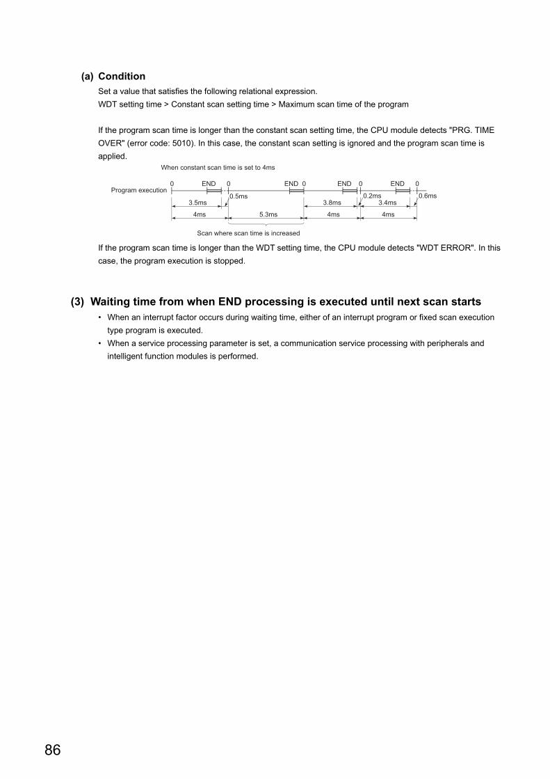
(a) Condition
Set a value that satisfies the following relational expression.
WDT setting time > Constant scan setting time > Maximum scan time of the program
If the program scan time is longer than the constant scan setting time, the CPU module detects "PRG. TIME
OVER" (error code: 5010). In this case, the constant scan setting is ignored and the program scan time is
applied.
If the program scan time is longer than the WDT setting time, the CPU module detects "WDT ERROR". In this
case, the program execution is stopped.
(3) Waiting time from when END processing is executed until next scan starts• When an interrupt factor occurs during waiting time, either of an interrupt program or fixed scan execution
type program is executed.
• When a service processing parameter is set, a communication service processing with peripherals and
intelligent function modules is performed.
0 0 END 0END 0END 0END
3.5ms
4ms 4ms
3.8ms 3.4ms
4ms5.3ms
0.2ms0.5ms 0.6ms
When constant scan time is set to 4ms
Program execution
Scan where scan time is increased
86

CHAPTER 3 CPU MODULE FUNCTIONS
3
3.3
Wa
tchd
og
Tim
er (W
DT
)
3.3 Watchdog Timer (WDT)
WDT is an internal timer of the CPU module that detects CPU module hardware failures and program errors.
(1) SettingOpen the tab for watchdog timer setting. The setting range is 10 to 2000ms (in increments of 10ms). 200ms is set
by default.
Project window [Parameter] [PLC Parameter] [PLC RAS]
A precision error is observed within the range of 0 to 10ms.
(2) ResetWDT is reset in END processing. The watchdog timer times up when the scan time is extended due to a factor
such as an interrupt, and the END/FEND instruction were not executed within the setting value of watchdog timer.
When the watchdog timer times up, "WDT ERROR" is detected and the following status occurs.
• The CPU module turns off all outputs.
• The RUN LED turns off and the ERR.LED starts flashing.
• SM1 turns on and the error codes 5000 and 5001 are stored in SD0.
The watchdog timer can be reset by executing the WDT instruction in a program. To avoid the time up of
watchdog timer while a program is repeatedly executed between the FOR and NEXT instructions, reset the
watchdog timer by the WDT instruction.
Note that the scan time value is not reset even after the watchdog timer is reset. The scan time is measured up to
the END instruction.
Enter a value.
Repeatedly executed program
WDT reset
Repeated by
1,000 times.
87

3.4 Latch Function
This function holds data in each device of the CPU module when:
• the CPU module is powered off and then on,
• the CPU module is reset, or
• a power failure occurred exceeding the allowable momentary power failure time.
Data in each device of the CPU module are cleared and set back to its default (bit device: off, word device: 0) when
this function is not used. By using this function, the operation can be continued with the previous data even after
powering off the CPU module while the data are managed by a sequential control. Program operation does not change
regardless of the latch
(1) Devices that can be latchedSet the device to latch among the following. (By default, only the latch relay is latched.)
The following devices also can be set when a file register is set to be used in the PLC file.
When the battery life-prolonging function is set, the latch function is disabled. ( Page 198, Section 3.33)
(2) Latch range settingSet the following.
Project Window [Parameter] [PLC Parameter] [Device]
• Latch clear operation enable range (Latch (1) Start/End): Data in this range can be cleared by a latch clear
operation.
• Latch clear operation disable range (Latch (2) Start/End): Data in this range cannot be cleared by a latch
clear operation.
• Latch relay (L) • Link relay (B) • Annunciator (F)
• Edge relay (V) • Timer (T) • Retentive timer (ST)
• Counter (C) • Data register (D) • Link register (W)
• File register (ZR) • Extended data register (D) • Extended link register (W)
Set latch ranges by the start and
end device numbers.
88

CHAPTER 3 CPU MODULE FUNCTIONS
3
3.4
La
tch F
un
ction
(3) Effect on the scan timeData latch processing is performed during END processing therefore the scan time increases. Consider the effect
on the scan time when latching devices. ( Page 378, Appendix 3.1)
To reduce the scan time increase due to latch*1, minimize the number of latch points (latch (1) setting, latch (2) setting, and latch relay) as much as possible by performing the following.
• Move data to be latched to the file register.• Store device data that is less frequently updated in the standard ROM with the SP.DEVST instruction. (The device
data stored in the standard ROM can be read with the S(P).DEVLD instruction. ( Page 180, Section 3.29)
*1 For file registers (including an extended data register (D) and an extended link register (W)), the scan time is not increased due to latch.
(4) Latch data clear methods
(a) Data in the latch clear operation enable range (Latch (1) Start/End)
Perform either of the following.
Data can be cleared only when the CPU module is in STOP status. If the operation is performed when the CPU module is not in STOP status, no processing is performed (data cannot be cleared).
Remark
Before clearing data by using the special relay and special register areas, check the version of the CPU module used.( Page 376, Appendix 2)
• Remote latch clear
Perform the operation using a programming tool. ( Page 117, Section 3.12.4)
• Latch clear by using the special relay and special register areas
1. Change the operating status of the CPU module to STOP.
2. Set "5A01H" in SD339.
3. Turn on SM339.
89

(b) Data in the latch clear operation disable range (Latch (2) Start/End) and in the file
register
Perform any of the following.
• Perform the data clear operation using the display unit. ( Page 249, Section 4.2.2)
• Reset data by using the RST instruction.
• Transfer K0 by using the MOV or FMOV instruction. ( MELSEC-Q/L Programming Manual (Common
Instruction))
• Set parameters ("Clear Device's whole Memory" or "Clear all File Registers").
[Online] [PLC Memory Operation] [Clear PLC Memory] "Clear Device's whole
Memory"/"Clear all File Registers"
(5) Precautions• The latch setting does not take effect if the device is specified as a local device or the initial device value is
specified for the device.
• A battery is required to retain the device data that are set in the latch range. If the battery connecter is
removed during power-off, the device data within the latch range are discarded and undefined values may
replace. (A battery is required also in the boot operation to latch devices.)
90

CHAPTER 3 CPU MODULE FUNCTIONS
3
3.5
Initia
l De
vice V
alu
e
3.5 Initial Device Value
This function registers data used in a program to the device or the buffer memory of the intelligent function module
without a program. By using this function, creating a device data setting program can be omitted in the initial
processing program.
(1) Timing when initial device values are written to the specified deviceThe CPU module writes data in the specified initial device value file to the specified device or the buffer memory
of the intelligent function module when:
• the CPU module is powered off and then on,
• the CPU module is reset, or
• the CPU module status is switched from STOP to RUN.
(2) Devices that can be used*1
The following shows devices that can be used for initial device value.
*1 The initial device value setting has a priority over the latch setting.*2 To use an intelligent function module, select "Module Synchronization" because the initial device value may not be
correctly set to the target module. ( Page 350, Appendix 1)
• Current timer value (T) • Current retentive timer value (ST)
• Current counter value (C) • Data register (D)
• Link register (W) • Link special register (SW)
• Special register (SD) • Intelligent function module device (U\G)*2
• File register (R, ZR) • Extended data register (D)
• Extended link register (W)
Using an initial device value can omit creating device data
setting program in an initial processing program.
Initial device value Device memory
Device memory
91

(3) Initial device value setting1. Specify a memory and name to store initial device
values.
Project Window [Parameter] [PLC
Parameter] [PLC File]
2. Specify a name to store initial device values.
Project Window [Device Initial Value] Right-
click [Add New Data...]
3. Clicking the button on the dialog box
above opens the dialog box shown on the left. Enter
the range for initial device values.
92

CHAPTER 3 CPU MODULE FUNCTIONS
3
3.5
Initia
l De
vice V
alu
e
Whenever the initial device value range is changed, execute "Device Memory Diversion" on the "Device Initial Value MAIN" dialog box. For details on creating initial device value data, refer to the following.Manual for the programming tool used
(4) PrecautionsInitial device values also take effect when the CPU module status is switched from STOP to RUN. Therefore,
they cannot be used for the data that are to be changed in a program after being set at CPU module power-on
from off. Use an instruction such as the MOV instruction in the main routine program so that the initial device
values are set to the specified devices. For the intelligent function module, use the TO instruction to write data to
the buffer memory.
4. Configure the device memory.
Project Window [Device Memory] [MAIN]
Right-click [Input Device...]
5. Store the initial device value file in the program
memory of the CPU module, standard ROM, or an
SD memory card.
[Online] [Write to PLC]
93

3.6 Service Processing Setting
This function allows to set the time and the number of times of service processing performed at END processing by
parameters.
Processing for requests from peripherals to the CPU module are performed with this function. The processing speed
for the communication response to the requests varies depending on the scan time and communication load. Set the
parameter of the service processing time as follows to achieve an optimal service processing environment for the
system used.
• Setting a longer time can improve the processing speed for the communication response.
• Setting a shorter time can avoid a prolonged scan time caused by the service processing.
Communications from multiple peripherals to the CPU module may slow down the processing speed for the
communication response. Adjust the settings for the system by specifying a longer service processing time or
modifying the parameter settings of the peripherals to set longer timeout times taking the processing speed for the
communication response and increases in scan times into consideration.
● The service processing setting can be configured for the following communications:• Communication via an intelligent function module (not including refresh with a network module)• Communication via a USB cable, RS-232 adapter, RS-422/485 adapter, and the built-in Ethernet ports
(communication with a programming tool or GOT, or using the built-in Ethernet function)
● Using the COM instruction enables the service processing during program execution while the processing is normally performed during END processing. Use this function when the scan time is long.
94

CHAPTER 3 CPU MODULE FUNCTIONS
3
3.6
Se
rvice P
roce
ssing
Se
tting
(1) Setting methodConfigure the setting of the service processing.
Project Window [Parameter] [PLC Parameter] [PLC System]
"Execute the process as the scan time proceeds" is selected by default.
*1 There is a margin of error between -20s to +30s against actual processing time.*2 The response performance of service processing significantly reduces in the following cases. Set service processing
time considering the time-out time of the peripheral. Service processing time is set much shorter than the scan time. Setting "Execute it while waiting for constant scan setting" results in increase in the scan time and decrease in the service processing time.
*3 For the following functions, scan time will be increased longer than the specified time during service processing even if the service processing time specification is set. Online change Change T/C setting Local device monitor Program memory backup Writing to/reading from the file register or the buffer memory of an intelligent function module (The scan time is increased when the write or read size is large.) Diagnostic function of a network module (CC IE Field diagnostics, CC-Link/ CC-Link/LT diagnostics) Monitor function (module access device, link direct device)
*4 Note that the scan time is increased much longer if the CPU module simultaneously receives multiple requests while the service processing count specification is set many.
*5 If a data communication is performed over Ethernet when "Specify service process execution counts" is selected in parameter, the scan time will increase by the service processing time (approx. 500ms). To keep the scan time 500ms or less, select an item other than "Specify service process execution counts" in parameter. (For example, select "Specify service process time." and set a time value to 500ms or less.)
*6 If communications in the MC protocol are performed with an item other than "Specify service process execution counts" selected, data inconsistency may occur. To prevent data inconsistency, select "Specify service process execution counts".
Item Description Setting range Remarks
Execute the process as the
scan time proceeds*6
Set the percentage of service processing for
one scan.
• Range: 1 to 99%
• Unit: 1%Default when selected = 10%
Specify service process time *1*2*3*6
Set the time of service processing for one scan.• Range: 0.2ms to 1000ms
• Unit: 0.1msDefault when selected = 0.2ms
Specify service process
execution counts*4*5
Set the number of service processing for one
scan.
• Range: 1 to 10 times
• Unit: 1 timeDefault when selected = 1 time
Execute it while waiting for
constant scan setting.*2*6
Set whether to perform service processing
during waiting time for constant scan setting.
Even when the waiting time is 0.2ms
or less, the service processing time of
0.2ms is added to the scan time.
Select any one option button.
Deselected parameters remain
unavailable.
95

(2) Operation for service processing settingOperations for each service processing setting is described below.
(a) Execute the process as the scan time proceeds
Operation when 10% is set is as shown below.
● When the constant scan is set, ( Page 99, Section 3.6 (2) (d)), the calculation of the service processing time is a calculation of the percentage of the time excluding the waiting time of the constant scan from the scan time, not a calculation of the percentage of the scan time.Example: Operation when 50% is set
● If no request data for service processing exists, END processing speeds up by the amount of request processing time. (The CPU module does not wait for requests.)
Program execution
END processing Request 1)
Program execution
END processing Request 2)-1
Program execution
END processingRequest 3)
Peripheral
Request 2)-2
1ms
1ms
1.2ms
The service processing time depends on the
scan time (program execution time).
When time required for processing one request exceeds 10% of one scan time, the service processing is suspended and the remaining requests are processed at the END processing in the next scan.
1st scan
(10ms)
2nd scan
(10ms)
3rd scan
(12ms)
Request 1)
Request 2)
Request 3)
Request 4)
Request 5)
Program execution
END processing
Waiting timeService processing
0% 50% 100%
Scan time (constant scan setting)
Service processing time
96

CHAPTER 3 CPU MODULE FUNCTIONS
3
3.6
Se
rvice P
roce
ssing
Se
tting
(b) Specify service process time
Operation when 1ms is set is as shown below.
If no request data for service processing exists, END processing speeds up by the amount of request processing time. (The CPU module does not wait for requests.)
Program execution
END processing Request 1)
Program execution
END processing
Peripheral
Program execution
END processing
Request 2)
Request 2)
Request 3)
1ms
Request 3)
Request 4)
Multiple requests are processed until the processing time exceeds the set service processing time (1ms).When the service processing time is exceeded, the service processing is suspended and the remaining requests are processed at the END processing in the next scan.
Regardless of the number of requests to be processed in the END processing, the increase in scan time will be kept constant.
Request 1)Request 2)
Request 3)Request 4)
Request 5)
1st scan
2nd scan
3rd scan
97

(c) Specify service process execution counts
Operation when 1 time is set is as shown below.
Operation when 2 times is set is as shown below.
● When several devices are connected to one CPU module, each device requests service processing. When the CPU module simultaneously receives requests from several devices, a single END processing can simultaneously accept several requests if the service processing count is set to the number of connected devices. This improves response performance. Note that the scan time increases by the amount of service processing time.
● If no request data for service processing exists, END processing speeds up by the amount of request processing time. (The CPU module does not wait for requests.)
Program execution
END processing Request 1)
Program execution
END processing Request 2)
Program execution
END processing Request 3)
Peripheral
Regardless of request data size, one
request is processed at one END processing.
Even if the program execution time is the same,
the scan time depends on service processing time.
Request 1)
Request 2)
Request 3)
Request 4)
Request 5)
1st scan
2nd scan
3rd scan
Program execution
END processing
Request 1)
Program execution
END processing
Request 2)
Request 3)
Peripheral
Request 4)
Regardless of request data size, two requests
are processed at one END processing.
Request 1)
Request 2)
Request 3)
Request 4)
Request 5)
1st scan
2nd scan
98

CHAPTER 3 CPU MODULE FUNCTIONS
3
3.6
Se
rvice P
roce
ssing
Se
tting
(d) Execute it (service processing) while waiting for constant scan setting.
● When setting the constant scan, selecting "Execute it while waiting for constant scan setting." can perform the service processing efficiently.
• When "Execute it while waiting for constant scan setting." is selected
• When "Execute the process as the scan time proceeds." is selected (50% is set.)
● Even when there is no waiting time, the service processing (0.2ms) is performed. Therefore, when the waiting time is less than 0.2ms, the constant scan time may be exceeded.
Program execution
Waiting time
END processing
Program execution
END processing
Peripheral
Request 1)
Request 2)
Request 3)
Request 4)Waiting time
The service processing is performed
during waiting time.
Constant scan
Constant scan
Request 1)
Request 2)
Request 3)
Request 4)
Request 5)
Program execution
END processing
Waiting time
Service processing
Scan time (constant scan setting)
Service processing time
Program execution
END processing
Waiting timeService processing
0% 50% 100%
Scan time (constant scan setting)
Service processing time
99

(e) Precautions
The following describes precautions for the service processing setting.
• In the service processing, the processing for request data from each receiving port (each intelligent function
module, USB, RS-232, and built-in Ethernet) is performed one by one. If several requests are received one
after another from the same receiving port, the service processing may not be performed in the same scan
even if the service processing time is left. For this reason, in communications with multiple peripherals via
the built-in Ethernet port, response times to each peripheral may not be improved, regardless of the service
processing time setting. In this case, divide connections of peripherals into the Ethernet module and the
built-in Ethernet of the CPU module to improve the response time.
• Since the processing for a request including accesses to files takes time, responding to the request
necessarily takes time. The processing for request data is performed one by one in the service processing,
and therefore responses to succeeding request data delays when the CPU module receives a request
including accesses to files. For this reason, set a longer timeout time for peripherals when using a system
that regularly send these requests.
100

CHAPTER 3 CPU MODULE FUNCTIONS
3
3.7
Ou
tpu
t Mo
de
at O
pe
ratin
g S
tatu
s Ch
an
ge
(ST
OP
to R
UN
)
3.7 Output Mode at Operating Status Change (STOP to RUN)
When the operating status is changed from RUN to STOP, the CPU module internally stores the outputs (Y) in the
RUN status and then turns off all the outputs (Y). Therefore, status of the outputs(Y) can be selected for setting when
the CPU module is set back to the RUN status.
• Output the output (Y) status prior to STOP. ("Previous state")
• Clear the output (Y) status. ("Recalculate (output is 1 scan later)")
(1) Operation when the operating status is changed from STOP to RUNOperations are explained using the holding circuit below.
(a) When outputting the output (Y) status prior to STOP
The CPU module outputs the output (Y) status immediately before the CPU module is changed to the STOP
status, and then performs program operations.
When the output (Y) status is forcibly turned on while the CPU module is in the STOP status, the CPU module
outputs the previous output (Y) status. The on status is not held if the output (Y) status before the CPU module
is changed to STOP status is off.
(b) When clearing output (Y) status
All outputs are turned off. The CPU module outputs the output (Y) status after program operations are
completed.
When the output (Y) status is forcibly turned on while the CPU module is in the STOP status, the CPU module
holds the on status.
(2) Setting procedureConfigure the setting under "Output Mode at STOP to RUN"
Project Window [Parameter] [PLC Parameter] [PLC System]
OFF
OFF
ON
ON
OFF
X21
Y0
X20
RUN STOP STOP RUN
OFF
OFF
ON
ON
OFF
X21
Y0
X20
RUN STOP STOP RUN
Select either of
these.
101

3.8 Input Response Time Setting
This function changes the input response time for each input module. Input modules obtain external inputs within the
set response time.
For the input response time setting by the built-in I/O function, refer to the following.
MELSEC-L CPU Module User's Manual (Built-In I/O Function)
(1) Setting procedure
1. Select "Input" under "Type" in the I/O Assignment tab, and click the button.
Project Window [Parameter] [PLC Parameter] [I/O Assignment]
2. Select any of the following values for "I/O Response Time". (Default: 10ms)
1ms, 5ms, 10ms, 20ms, 70ms
The shorter the input response time is, the more the CPU module is susceptible to noise. Consider the operating environment when setting input response time values.
OFF
OFF
ON
ONExternal input
Input module
Input response time
102

CHAPTER 3 CPU MODULE FUNCTIONS
3
3.9
Erro
r Tim
e O
utp
ut M
od
e S
ettin
g
3.9 Error Time Output Mode Setting
This function determines the output mode (clear or hold) from the CPU module to output modules and intelligent
function modules when a stop error occurs in the CPU module.
For the error time output mode setting by the built-in I/O function, refer to the following.
MELSEC-L CPU Module User's Manual (Built-In I/O Function)
(1) Setting procedure
1. Select a target module under "Type" in the I/O Assignment tab, and click the button.
Project Window [Parameter] [PLC Parameter] [I/O Assignment]
2. Select either of the following items for "I/O Response Time".
"Clear" or "Hold"
103

3.10 PLC Operation Mode at H/W Error Setting
This function determines an operation mode of the CPU module when a hardware error (CPU module detects SP.UNIT
DOWN) occurred in an intelligent function module.
(1) Setting procedure
1. Select "Intelligent" under "Type" in the I/O Assignment tab, and click the button.
Project Window [Parameter] [PLC Parameter] [I/O Assignment]
2. Select either of the following items for "PLC Operation Mode at H/W error".
"Stop" or "Continue"
104

CHAPTER 3 CPU MODULE FUNCTIONS
3
3.1
1 S
ecu
rity Fu
nctio
n3
.11
.1 F
ile P
assw
ord
32
3.11 Security Function
This function protects data in the CPU module against tampering and theft by unauthorized persons. Use the following
functions according to your applications and needs.
3.11.1 File Password 32
This function sets write password and read password for each file stored in the CPU module so that files are protected
against tampering and theft by unauthorized persons.
(1) File protection timingFile protection is enabled immediately after the passwords are registered, and it is disabled immediately after the
passwords are deleted.
(2) Password target filesA password can be set to the following files.
• Program
• Device comment
• Initial device value
• Parameter
• Source information
Function Purpose Reference
File password 32 To limit access to each file in the CPU module Page 105, Section 3.11.1
Remote password To limit access to the CPU module from external devices. Page 110, Section 3.11.2
Block password To limit access to each POUGX Works2 Version 1 Operating Manual
(Common)
Read password "XYZ98756" is authenticated.
Programming tool
File A can be read since the password matches.
CPU module
File A
Write password: AbcDEF12
Read password: XYZ98756
A write password and read
password can be set individually.
File A cannot be written since
the password does not match.
Programming tool
Write password "1234abCD" is authenticated.
105

(3) Operations that are controlled and the number of charactersA password can be set to the following operations. The minimum number of characters in the password should
be 4, and the maximum number should be 32.
• Reading files
• Writing files
• Reading/writing files
Remark
For characters allowed in passwords, refer to "Explanation of Registration Conditions" on the Input Password window.
(4) Online operations that require authenticationAuthentication is required to execute the following operations to password-protected files.
( Page 108, Section 3.11.1 (7))
• Write to PLC (data writing)
• Read from PLC (data reading)
• Online change (data writing)
• Change TC setting value (data writing)
• Verify with PLC (data reading)
• Create/Change or Delete of a password (data reading and writing)
• Delete PLC data (data writing)
(5) Operating procedureTo change, delete, or unlock the password, refer to the following.
Manual for the programming tool used
106

CHAPTER 3 CPU MODULE FUNCTIONS
3
3.1
1 S
ecu
rity Fu
nctio
n3
.11
.1 F
ile P
assw
ord
32
(6) Precautions
(a) Boot from an SD memory card
The following table shows the relationship between the boot operation availability and file password 32 setting.
: No combination available
If boot file settings are configured to more than one file, the files can be transferred only when all the
passwords match. If all the passwords do not match, data in the SD memory card are not transferred and
"BOOT ERROR" (error code: 2213) occurs.
(b) When "Clear Program Memory" is selected in parameter (Boot File tab)
Even when a password is registered, files will be formatted.
Transfer source file Transfer destination filePassword status Boot operation
File Password File Password
Exist
SetExist
SetMatched Enabled
Not matched Disabled
Not set Disabled
Not exist Enabled
Not setExist
Set Disabled
Not set Enabled
Not exist Enabled
Not exist
107

(7) Authentication methodPasswords are authenticated in three ways.
• By a programming tool
• By the FTP server
• By the MC protocol
(a) Authentication by a programming tool
The entered password is valid until the project is closed.
1. Whenever an online operation requiring password
authentication is executed, the "Disable Password"
window appears. Select an authentication target file,
and click the button.
2. Enter a password in the "Input Disable Password"
window.
108

CHAPTER 3 CPU MODULE FUNCTIONS
3
3.1
1 S
ecu
rity Fu
nctio
n3
.11
.1 F
ile P
assw
ord
32
(b) Authentication by the FTP server
To access a password-protected file from external devices using the FTP server function, password
authentication is required for each file. To change a file to access, password authentication is required again.
: Authentication required, : Authentication not required
To authenticate a password, use FTP commands for password authentication.
For details on commands, refer to the following.
MELSEC-L CPU Module User's Manual (Built-In Ethernet Function)
(c) Authentication by the MC protocol
To access a password-protected file from external devices using the MC protocol, the request message format
of the MC protocol must be changed and a command for the file password 32 must be specified.
1. Add "Keyword" at the end of the request message, and set a password in that area.
2. Authenticate the password using the password set to "Keyword"
3. For the commands requiring password authentication, specify 0004 (for file password 32) in the
"Subcommand" area of a request message.
For details, refer to the following.
MELSEC Communication Protocol Reference Manual
Operation CommandPassword authentication
Data write Data read
Deleting a file in a CPU module delete
Reading a file from a CPU module get
Deleting a file in a CPU module mdelete
Reading a file from a CPU module mget
Changing the file name in a CPU module rename
Changing or displaying the file attribute in a CPU module change
Operation Command name
Disable Password (Write) quote passwd-wr <password>
Disable Password (Read) quote passwd-rd <password>
Function Command (subcommand)
File delete 1822 (0004)
File attribute change 1825 (0004)
File copy 1824 (0004)
File open 1827 (0004)
109

3.11.2 Remote Password
This function prevents unauthorized access to the CPU module from external devices.
(1) Settable modules and the number of settable modulesThe following shows the modules for which the remote password can be set and the number of settable modules.
(The number of settable modules does not indicate the number of connectable modules in the system where a
CPU module is used.)
• CPU module (Built-in Ethernet port): 1
• Serial communication module: 8
• Ethernet module: 8
Remark
For details on the remote password for a serial communication module or Ethernet module, refer to the manual of each module.
(2) Flow from remote password setting to reflection of the password
1. Register a remote password. ( Page 375, Appendix 1.4)
Project window [Parameter] [Remote Password]
2. Write it to the CPU module. (Write to PLC)
The remote password is transferred to the target module when:
• the CPU module is powered off and then on or
• the CPU module is reset.
A remote password proceeds the lock processing so that the access is limited. Only when the entered remote
password matches with the registered password, access is allowed (unlock processing (cancel)).
Checks the remote password.
1) Register a remote password.
2) Write the password to the CPU module
Ethernet
CPU module
Programming tool
3) The remote password is transferred
when the CPU module is powered off and
then on or is reset.
110

CHAPTER 3 CPU MODULE FUNCTIONS
3
3.1
1 S
ecu
rity Fu
nctio
n3
.11
.2 R
em
ote
Pa
sswo
rd
(3) Changing/deleting a remote passwordOpen the "Remote Password Setting" dialog box. ( Page 375, Appendix 1.4)
Project window [Parameter] [Remote Password]
• To change a remote password, write the new remote password to the CPU module.
• To delete a remote password, click the button and write the remote password to the CPU module.
For a Ethernet Built-in CPU,
configure the "Detail" setting.
Enter a remote password.
111

3.12 Remote Operation
Remote operation allows externally (by programming tool, external devices using the MC protocol, or using remote
contacts) changing the operating status of the CPU module. There are four types of remote operations:
• Remote RUN/STOP ( Page 112, Section 3.12.1)
• Remote PAUSE ( Page 114, Section 3.12.2)
• Remote RESET ( Page 116, Section 3.12.3)
• Remote latch clear ( Page 117, Section 3.12.4)
(1) The relationship between a CPU module and a remote operation.Availability of remote operations varies depending on the status of a CPU module.
*1 Including the stop error status of the CPU module.
3.12.1 Remote RUN/STOP
This operation externally changes the operating status of the CPU module to RUN or to STOP, keeping the switch of
the CPU module in the RUN position.
This operation is useful when:
• the CPU module is inaccessible, or
• changing the status of a CPU module that is in a control panel to RUN or STOP by external signals.
(1) Program operation
(a) Remote RUN
The CPU module changes its operating status to RUN and executes a program from the step 0. (The remote
RUN operation must be performed to the CPU module whose operating status has been changed to STOP by
the remote STOP operation.)
(b) Remote STOP
The CPU module executes a program until the END instruction and changes its operating status to STOP.
(2) Executing methodThe following three methods are available.
• Using a RUN contact
• Using a programming tool
• By an external device using the MC protocol
• Using the link dedicated instruction of the CC-Link IE Field Network master/local module
CPU module statusRemote operation
Remote RUN Remote STOP Remote PAUSE Remote RESET Remote latch clear
RUN status RUN status STOP status PAUSE status Not operable Not operable
STOP status STOP status STOP status STOP status Reset*1 Latch clear
112

CHAPTER 3 CPU MODULE FUNCTIONS
3
3.1
2 R
em
ote
Op
era
tion
3.1
2.1
Re
mo
te R
UN
/ST
OP
(a) Using a RUN contact
Set a RUN contact.
Project window [Parameter] [PLC Parameter] [PLC System]
The remote RUN/STOP operation can be performed by turning on/off the set RUN contact.
• When the RUN contact is turned off, the CPU module status changes to RUN.
• When the RUN contact is turned on, the CPU module status changes to STOP.
(b) Using a programming tool
Open the "Remote Operation" dialog box.
[Online] [Remote Operation]
A remote RUN operation executed only from the programming tool that has executed a remote STOP operation to the CPU module.
(c) By an external device using the MC protocol
Use MC protocol commands.
MELSEC Communication Protocol Reference Manual
(d) Using the link dedicated instruction of the CC-Link IE Field Network master/local
module
Use the link dedicated instruction of the CC-Link IE Field Network master/local module.
MELSEC-L CC-Link IE Field Network Master/Local Module User's Manual
Set a device used as a contact.
Select "RUN" or "STOP"
for execution.
113

3.12.2 Remote PAUSE
This operation externally changes the operating status of the CPU module to PAUSE, keeping the CPU module switch
in the RUN position.
PAUSE status is a status where program operations in the CPU module are stopped, holding the status (on or off) of all
outputs (Y).
This operation is useful, especially during the process control, to hold the on status of outputs (Y) even after the
operating status of the CPU module is switched from RUN to STOP.
(1) Executing methodThere are three methods for performing the remote PAUSE operation.
• Using a PAUSE contact
• Using a programming tool
• By an external device using the MC protocol
(a) Using a PAUSE contact
Set a PAUSE contact.
Project window [Parameter] [PLC Parameter] [PLC System]
When setting a PAUSE contact, set a RUN contact as well. (Setting of only a PAUSE contact is not allowed.)
Set a device used as a contact.
OFF
ON
0 END
PAUSE status
0 END 0 0END END
PAUSE enable coil (SM206)OFF
ON
PAUSE contact (SM204)OFF
ON
RUN/PAUSE status RUN RUNPAUSE
Turns on at execution of the END
processing in the scan where set
PAUSE contact and SM206 turn on.
The CPU module enters the PAUSE status and
stops operation when an operation is processed up
to the END instruction in the scan next to the one
where the PAUSE contact turns on.
Turning off the PAUSE contact or SM206 will
exit the PAUSE status and restart program
operation from step 0.
Set PAUSE contact
114

CHAPTER 3 CPU MODULE FUNCTIONS
3
3.1
2 R
em
ote
Op
era
tion
3.1
2.2
Re
mo
te P
AU
SE
(b) Using a programming tool
Open the "Remote Operation" dialog box.
[Online] [Remote Operation]
(c) By an external device using the MC protocol
Use MC protocol commands.
MELSEC Communication Protocol Reference Manual
(2) When forcibly keeping output statusTo forcibly keep the output status (on or off) in the PAUSE status, provide an interlock with the PAUSE contact
(SM204).
Select "PAUSE" for execution.
In the PAUSE status, on/off status of
Y70 depends on that of M20.
Turns off in the PAUSE status.
Turns on in the PAUSE status.
115

3.12.3 Remote RESET
This operation externally resets the CPU module when the CPU module is in the STOP status. Even if the switch of the
CPU module is in the RUN position, this operation can be performed when the module is stopped due to an error.
Use this function when an error occurred in the CPU module that is beyond the reach.
(1) Executing methodThere are two methods for performing the remote RESET operation.
• Using a programming tool
• By an external device using the MC protocol
Before performing the remote RESET operation, select the "Allow" checkbox for the remote RESET operation in
the PLC System tab of the PLC Parameter dialog box, and then write the parameter setting to the CPU module.
Project window [Parameter] [PLC Parameter] [PLC System]
(a) Using a programming tool
Open the "Remote Operation" dialog box.
[Online] [Remote Operation]
(b) By an external device using the MC protocol
Use MC protocol commands.
MELSEC Communication Protocol Reference Manual
(2) Status after reset processingWhen the remote RESET operation is completed, the CPU module will be placed in the operating status set by
the switch. Consider the operating status of the CPU module after the reset operation if the CPU module had
stopped due to an error.
(3) PrecautionsNote that the CPU module may not be reset by the remote RESET operation due to noise. In this case, reset the
CPU module using the switch or power off and then on the CPU module.
Select this checkbox before
performing remote RESET.
Select "RESET" for execution.
116
CHAPTER 3 CPU MODULE FUNCTIONS
3
3.1
2 R
em
ote
Op
era
tion
3.1
2.4
Re
mo
te L
atch
Cle
ar
3.12.4 Remote Latch Clear
This function resets the device data when the CPU module is in the STOP status. *1
This operation is useful when:
• the CPU module is inaccessible or
• externally performing latch clear to the CPU module in a control panel.
*1 Device data in the range where a latch clear operation is disabled cannot be reset. ( Page 89, Section 3.4 (4))
(1) Executing methodThe following two methods are available.
• Using a programming tool
• By an external device using the MC protocol
Set the CPU module in the STOP status. (Not available in the RUN status)
(a) Using a programming tool
Open the "Remote Operation" dialog box.
[Online] [Remote Operation]
(b) By an external device using the MC protocol
Use MC protocol commands.
MELSEC Communication Protocol Reference Manual
Select "Latch clear" for execution.
117

3.13 Scan Time Measurement
This function displays the processing time of set program section during ladder monitoring. The time required for the
subroutine and interrupt programs can be measured.
(1) Execution
1. Open the "Scan Time Measurement" dialog box.
[Debug] [Scan Time Measurement]
2. Specify the start and end steps and click the button.
When displaying the "Scan Time Measurement" dialog box after specifying the scan time measurement range in monitor mode, the start and end steps are set in the specified ranges such as shown below.
118

CHAPTER 3 CPU MODULE FUNCTIONS
3
3.1
3 S
can
Tim
e M
ea
sure
me
nt
(2) Precautions• The minimum unit of measurement time is 0.01ms. If the measurement time is less than 0.01ms, 0.000ms is
displayed.
• When between the FOR and NEXT instructions is specified, the execution time of one scan between the
specified steps is displayed.
• If a subroutine program call instruction (CALL instruction) exists within the scan time measurement range,
processing time for the subroutine program is included in the scan time.
• If an interrupt/fixed scan execution type program is executed within the scan time measurement range,
program execution time is added to the scan time.
• Scan time from one program file to another cannot be measured. Also, scan time cannot be updated on the
"Scan Time Measurement" dialog box in the following cases.
When the branch instruction is specified in the end step When only the start step is executed
Example: The JMP instruction is specified in the end step. Example: The specified end step is not executed by the JMP instruction.
When the end step is executed before the start step When the start step is executed continuously
Example: The start step is specified as the next step of the CALL instruction
and the end step is specified in a subroutine program executed by the CALL
instruction.
Example: Only the start step is specified between the FOR and NEXT
instructions.
Measurement range
Measurement range
Main
program
Subroutine
program
Start step: 3
End step: 6
End step: 9
Start step: 3
The end step is
skipped by the JMP
instruction.
Start step: 3
End step: 8
The start step is executed
after the end step by the CALL
instruction.
Start step: 8
End step: 13
The start step is executed
continuously since it is specified
between the FOR and NEXT
instructions.
119

When the IRET instruction, FEND instruction, BREAK instruction, or RET instruction is specified in the end step
Example: The IRET instruction is specified in the end step of an interrupt program by I31.
0
1
3
7
10
12
I31
FEND
END
IRET
EI
4
13
End step: 12
Start step: 4
When the scan time in an interrupt program is measured, do not specify the IRET instruction for the end step.
120
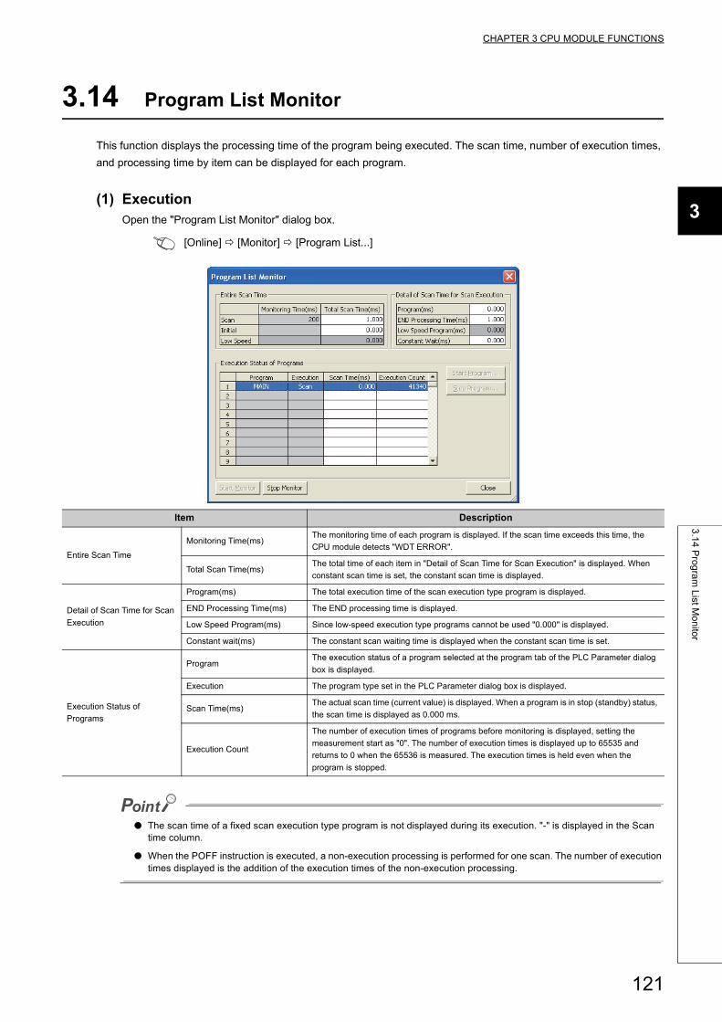
CHAPTER 3 CPU MODULE FUNCTIONS
3
3.1
4 P
rog
ram
List M
on
itor
3.14 Program List Monitor
This function displays the processing time of the program being executed. The scan time, number of execution times,
and processing time by item can be displayed for each program.
(1) ExecutionOpen the "Program List Monitor" dialog box.
[Online] [Monitor] [Program List...]
● The scan time of a fixed scan execution type program is not displayed during its execution. "-" is displayed in the Scan time column.
● When the POFF instruction is executed, a non-execution processing is performed for one scan. The number of execution times displayed is the addition of the execution times of the non-execution processing.
Item Description
Entire Scan Time
Monitoring Time(ms)The monitoring time of each program is displayed. If the scan time exceeds this time, the
CPU module detects "WDT ERROR".
Total Scan Time(ms)The total time of each item in "Detail of Scan Time for Scan Execution" is displayed. When
constant scan time is set, the constant scan time is displayed.
Detail of Scan Time for Scan
Execution
Program(ms) The total execution time of the scan execution type program is displayed.
END Processing Time(ms) The END processing time is displayed.
Low Speed Program(ms) Since low-speed execution type programs cannot be used "0.000" is displayed.
Constant wait(ms) The constant scan waiting time is displayed when the constant scan time is set.
Execution Status of
Programs
ProgramThe execution status of a program selected at the program tab of the PLC Parameter dialog
box is displayed.
Execution The program type set in the PLC Parameter dialog box is displayed.
Scan Time(ms)The actual scan time (current value) is displayed. When a program is in stop (standby) status,
the scan time is displayed as 0.000 ms.
Execution Count
The number of execution times of programs before monitoring is displayed, setting the
measurement start as "0". The number of execution times is displayed up to 65535 and
returns to 0 when the 65536 is measured. The execution times is held even when the
program is stopped.
121

3.15 Interrupt Program List Monitor
This function displays the number of executions of an interrupt program.
(1) ExecutionOpen the "Interrupt Program List Monitor" dialog box.
[Online] [Monitor] [Interrupt Program List...]
Item Description
Interrupt Pointer An interrupt pointer is displayed.
Execute CountThe number of executions of an interrupt program is displayed. This function starts counting after the
CPU module is in the RUN status. When the counting reaches 65536 times, it is reset to 0.
Comment Device comments created to an interrupt pointer is displayed.
122

CHAPTER 3 CPU MODULE FUNCTIONS
3
3.1
6 M
on
itor co
nd
ition
settin
g
3.16 Monitor condition setting
This function monitors the CPU module under specified conditions.
Remark
Before setting the monitor condition, check the version of the programming tool used.( Page 376, Appendix 2)
(1) Setting methodThe following two methods are available for the monitor condition setting.
• Monitor execution condition setting
• Monitor stop condition setting
For details on the setting method, refer to the following manuals.
Manual for the programming tool used
123

(a) When only a step number is specified
Monitor data is collected when the status immediately before execution of the specified step becomes the
specified status.
• When the operation of the specified step changes from the non-execution status to the execution status:
<>
• When the operation of the specified step changes from the execution status to the non-execution status:
<>
• Always when the operation of the specified step is being executed only: <ON>
• Always when the operation of the specified step is not being executed only: <OFF>
• Always regardless of the status of the operation of the specified step: <Always>
● If a step between the AND/OR blocks is specified as a monitor condition, monitor data is collected when the status immediately before execution of the specified step becomes the specified status by the LD instruction in the block. The monitoring timing depends on the ladder of the specified step. The following shows examples of monitoring when the step 2 is on (Step No. [2] = <ON>).
● When "0" is specified as the step No., set the condition to "Always".
Condition Description
When the step 2 is connected by the AND
instruction
When both X0 and X1 are on, the monitor execution condition is
established.
When the step 2 is connected in the middle of the
AND/OR block
When X1 is on, the execution condition is established. (The on/off status
of X0 does not affect the establishment of the monitor execution
condition.)
When the start of a ladder block other than the
step 0 is specified for the step number as a
detailed condition
Monitor data is collected when the execution status of the instruction
immediately before execution becomes the specified status. If (Step No.
[2] = <ON>) is specified in the following ladder, monitor data is collected
when OUT Y10 turns on.
0X0 X1 X2
Y20
0 LD XO
1 AND X1
2 AND X2
3 OUT Y20
Ladder mode List mode
Step 2
Ladder mode
Step 2
List mode
0 Y20 X0 X1 X2
X3
0 LD XO
1 LD X1
2 AND X2
3 OR X3
4 ANB
5 OUT Y20
0 Y10 X0
2 Y11 X1
0 LD XO
1 OUT Y10
2 LD X1
3 OUT Y11
Ladder mode List mode
124

CHAPTER 3 CPU MODULE FUNCTIONS
3
3.1
6 M
on
itor co
nd
ition
settin
g
(b) When only a device is specified
Either word device or bit device can be specified.
(c) When a step number and device are specified
Monitor data is collected when the status immediately before execution of the specified step becomes the
specified status or the status (current value) of the specified bit device (word device) becomes the specified
value.
If the rise of step 100 and D1 = 5 (Step No. [100] = <>, Word device [D1] = [K5]) are specified as the execution condition, the monitor execution condition is established on the rising edge of the step 100 and also D1=5.
The monitor interval of a programming tool depends on the processing speed of the programming tool. For the monitor execution conditions established at the interval shorter than the monitor interval of the programming tool, monitor is executed only when the monitor execution condition is established at the monitor timing of the programming tool.
• When a word device is specified
Monitor data is collected when the current value of the specified word device becomes the specified value.
Specify the current value in decimal or hexadecimal.
• When a bit device is specified
Monitor data is collected when the execution status of the specified bit device becomes the specified status.
Select the execution condition (on the rising edge or falling edge).
X0 M0Y20
INC D1
Step 100
X0
100 100 100 100
M0
D1=5
Step No.
Monitor timing
(CPU module)
125

(2) Precautions
(a) Files to be monitored
When monitoring after setting the monitor condition, the file displayed on a programming tool is monitored.
Match the name of the file to be monitored on the CPU module with that on the programming tool by executing
[Online] -> [Read from PLC].
(b) No file register setting
If the file register is monitored when there is no file register used, "FFFFH" is displayed.
(c) Device assignment
For a monitor operation, the device assignment in the CPU module and the programming tool must be the
same.
(d) Monitoring by multiple users simultaneously
When monitoring the buffer memory of an intelligent function module, the scan time increases as in case when
executing the FROM/TO instructions.
(e) Monitoring by multiple users simultaneously
The following precautions should be followed:
• High speed monitoring can be performed by increasing 1K step in the system area for every monitor file of
other stations when formatting the program memory or setting the Boot file of the PLC Parameter.. Up to
15 stations can be set as the station monitor file, however, the program area will be reduced by the files'
worth of areas.
• When the monitor condition or monitor stop condition is set, only one user can perform monitoring.
(f) Setting a monitor stop condition
A monitor stop condition can be set only in the ladder monitor.
(g) Specifying the same device as a condition
When specifying the same device as a monitor condition or monitor stop condition, set the on/off status as well.
(h) Specifying a step number as a monitor condition
If an instruction in the specified step is not executed in such cases described below, the monitor condition will
not be established.
• The specified step is skipped with the CJ, SCJ, or JMP instruction.
• The specified step is the END instruction and never be executed because the FEND instruction also exists
in the program.
(i) During monitor condition registration
Do not reset the CPU module while monitoring conditions are being registered.
126

CHAPTER 3 CPU MODULE FUNCTIONS
3
3.1
6 M
on
itor co
nd
ition
settin
g
(j) Monitor operation with monitor condition setting
When monitor operation with monitor condition setting is performed, other applications on the same personal
computer cannot execute any online function using the same route for the monitor operation. The following
shows examples of other applications:
• Programming tool
• Applications using MX Component
• MX Sheet
If any online function is executed by other applications using the same route for the monitor operation, the
following situations may occur.
• No response comes back from the CPU module to the online function. (A time-out occurs in the online
communication function with the CPU module.)
• The CPU module detects an error (error code: 4109) for the online function executed.
• Even when the monitor condition is established in the CPU module, monitoring results cannot be updated
for the monitor operation with monitor condition setting.
127

3.17 Local Device Monitor/Test
This function enables debugging of local devices of the program that is being monitored.
(1) Monitoring local devicesThe following shows examples of monitoring local devices.
Ex. D0 to D99 are set as local devices and three programs "A", "B" and "C" are executed by the CPU module.
(Three programs are to be executed in the order of A B C (END processing) A B....)
*1 When "Not Used" is set for "Local Device" in File Usability Setting of the Program tab, the D0 value after execution of the specified program is monitored.
When local devices are set to be monitored and the program "B" is displayed for monitoring, the local device(s)
ItemMonitored device
D0 (Local device) D100 (Global device)
Local device monitor is setThe D0 value in the specified program (local
device for a program) is monitored.*1The D100 value after execution of the specified
program is monitored.
Local device monitor is not setThe D0 value after execution of the program "C"
is monitored.
The D100 value after execution of the program
"C" is monitored.
128

CHAPTER 3 CPU MODULE FUNCTIONS
3
3.1
7 L
oca
l De
vice M
on
itor/T
est
used in the program "B" can be monitored.CPU module
Program execution (A B C)
Program: A
Program: B
Program: C
Set local device monitor and monitor the program B.
Programming tool
Display the local device data of the program B.
If D0 to D99 are set as a local device, D0 = 4 and D99 = 8 are displayed when X10 and X11 are on, respectively.
(Example)
129

(2) Device test procedure
1. Connect a personal computer to the CPU module
2. Display a program in ladder mode
3. Switching to the monitor mode
[Online] [Monitor] monitor mode
4. Select [Local device monitor] from the monitor window.
(3) Number of programs that can be monitored/testedLocal devices of 16 programs can be simultaneously monitored or tested from multiple programming tools.
(4) Precautions• One programming tool can monitor or test local devices in one program at a time. Local devices in multiple
programs cannot be monitored or tested simultaneously.
• When local devices in a stand-by type program are monitored, data in local devices are saved and restored.
For this reason, the scan time increases.
• When local devices in a fixed scan execution type program are monitored, data in local devices cannot be
acquired and "0" is displayed.
130

CHAPTER 3 CPU MODULE FUNCTIONS
3
3.1
8 E
xtern
al In
pu
t/Ou
tpu
t Fo
rced
On
/Off
3.18 External Input/Output Forced On/Off
This function forcibly turns on or off the external input/output of the CPU module.
(1) Input/output operation when a forced on/off operation is performedThree types of forced on/off operations are available as shown in the following table. The following table shows
the status of input (X) and output (Y) when a forced on/off operation is performed. Note that a program operation
takes priority when a contact of output (Y) is used in the program.
The following shows the input/output operation when a forced on/off operation is performed.
(2) Specifications
(a) CPU module status
Forced on/off can be registered regardless of the operating status (RUN/STOP) of the CPU module. Note,
however, that only input can be forcibly turned on/off during a stop error. The CPU module outputs on/off data
only to device Y.
(b) Registerable devices
Forced on/off can be registered as many as the number of I/O device points in the CPU module.
(c) Target input/output
• Input (X) and output (Y) of modules used in the built-in I/O function.
• Input (X) and output (Y) of connected modules
• Input (X) and output (Y) of the CPU module to be refreshed from RX/RY of the CC-Link IE Field Network
master/local module or the CC-Link system master/local module (including built-in CC-Link function)
• Input (X) and output (Y) of the CPU module to be refreshed from RX/RY of CC-Link IE Field Network Basic
Operation Input (X) operation Output (Y) operation
Forced on registeredThe CPU module performs program operations
using inputs forcibly turned on.
The CPU module outputs "on" externally regardless of
the results of program operations.
Forced off registeredThe CPU module performs program operations
using inputs forcibly turned off.
The CPU module outputs "off" externally regardless of
the results of program operations.
Forced on/off cancellationThe CPU module performs program operations
using external inputs.
The CPU module outputs the results of program
operations externally.
Forced off of Y10
Forced off of X0
Output of Y10
(OFF)
Input of X0
(ON)
Remains on in a program even if forced off is executed. (external output is off.)
External input is forcibly turned off.
Output forced on/off operation
Output refresh
Input refresh
Input forced on/off operation
Program execution
External output (Y10 is off.)
External input (X0 is on.)
131

(d) Forced on/off timing
(e) Number of registerable devices
Up to 32 devices in total can be registered.
(f) Checking the execution status
• Reading the forced on/off registration status of a programming tool.
• Flashing of the MODE LED (green) (The MODE LED flashes in green when a device is registered.)
• The on status of the 1st bit in SD840 (Debug function usage).
When checking by the MODE LED or SD840, remind that they are also used to check the execution status of executional conditioned device tests. ( Page 135, Section 3.19)
(g) Forcibly turning on/off from multiple programming tools
Forced on/off can be registered to a single CPU module from multiple programming tools. In this case, the last
registration is effective. For this reason, the forced on/off status which is different from the status actually
registered in the CPU module may be displayed on the screen that registered forced on/off earlier. When the
forced on/off registration is performed from multiple programming tools, click the button to
update the data, and execute the function.
Refresh area Timing
• Input and output used in the built-in I/O
function.
• Input and output of modules connected
• During END processing (input refresh)
• At execution of the COM instruction (input refresh)
• At execution of an instruction using direct access input (DX) and direct access output
(DY)
• At execution of the RFS or MTR instruction
• At execution of an instruction used for a system
Input and output of the CPU module to be
refreshed from RX/RY of the CC-Link IE Field
Network master/local module or the CC-Link
system master/local module (including built-in
CC-Link function)
• During END processing (auto refresh)
• At execution of the COM instruction (auto refresh)
• At execution of the ZCOM instruction (auto refresh)
Input and output of the CPU module to be
refreshed from RX/RY of CC-Link IE Field
Network Basic
• During END processing (auto refresh)
• At execution of the COM instruction (auto refresh)
132

CHAPTER 3 CPU MODULE FUNCTIONS
3
3.1
8 E
xtern
al In
pu
t/Ou
tpu
t Fo
rced
On
/Off
(h) Status of devices after forced on/off registration data are canceled
*1 The result is output for one scan in accordance with the registered on/off state even after forced on/off registration data are canceled.
Forced on/off registered device Program operations (on/off) performedProgram operations (on/off) not
performed
Input
• Input used in the built-in I/O function
• Input from connected modules on the base
unit
Uses the on/off status input from modules.
Input of the CPU module to be refreshed from
RX of the CC-Link IE Field Network
master/local module or the CC-Link system
master/local module (including built-in CC-Link
function)
Uses the on/off status refreshed via CC-Link.
Input of the CPU module to be refreshed from
RX of CC-Link IE Field Network Basic
Uses the on/off status refreshed from the CPU module (when CC-Link IE Field Network Basic is
used)
Output other than above (outside of the refresh
range)Uses the results of program operations. Holds the forced on/off status.
Output
• Output used in the built-in I/O function.
• Output from connected modules on the base
unit.
Outputs the results of program operations.
Holds the registered on/off status.
Output of the CPU module to be refreshed
from RY of the CC-Link IE Field Network
master/local module or the CC-Link system
master/local module (including built-in CC-Link
function)
Output of the CPU module to be refreshed
from RY of CC-Link IE Field Network BasicOutputs the results of program operations.*1
Output other than above (outside of the refresh
range)
Outputs the results of program operations. (The
results are not output externally.)Holds the forced on/off status.
133

(3) Operating procedure
1. Open the "Forced Input Output Registration/Cancellation" dialog box.
[Debug] [Forced Input Output Registration/Cancellation...]
2. Enter the target device to the "Device" column.
3. Click the button for intended operation.
The latest on/off status can be checked by clicking the button.
Button name Description Button name Description
Registers forced on for a specified device. Cancels forced on/off registered for the device specified.
Registers forced off a specified device. Cancels all forced on/off registration.
134

CHAPTER 3 CPU MODULE FUNCTIONS
3
3.1
9 E
xecu
tion
al C
on
ditio
ne
d D
evice
Te
st
3.19 Executional Conditioned Device Test
This function changes a device value for the specified step of a program. This enables debugging of the specified
ladder block without modifying the program.
The executional conditioned device test is not available for the SFC program.
(1) Operation of the executional conditioned device testA device value is changed based on the registration data once the executional conditioned device test setting is
registered.
Note that a device value is changed in the specified step regardless of an execution status of the instruction in
the specified step.
(2) Applicable devicesThe following table shows the applicable devices and the number of settable devices.
Type Applicable deviceNumber of settable
devices
Bit device X (DX), Y (DY), M, L, B, F, SB, V, SM, T (contact), ST (contact), C (contact), FX, and FY
Up to 32 (in total)Word device
T (current value), ST (current value), C (current value), D, D (extended data register), SD, W, W
(extended link register), SW, R, ZR, Z, U\G, FD
Digit-specified bit device: X, Y, M, L, F, SM, V, B, SB
Indirect specification (@D0): D, SD, W, SW, R, ZR (devices specified with @)
Programming tool
Program
Step number
Device
Setting value
Execution timing
: MAIN
: 10
: M0
: ON
: Before instruction execution
Registration data
Turns on.
Program : MAIN
879
879
879
880
880880
879
[Program example] [Operation]
Processing LD M0
10 35
OFF
45
Changes the D0 value to "35".
+ K10 D0
D0 value
M0 value
Register executional conditioned device
test that sets "35" to D0 in this step.
A device value is changed at the specified
step regardless of the M0 value.
135

(3) How to check the execution status• By displaying the "Check/Disable Executional Conditioned Device Test Registration" dialog box
• By the flash of the MODE LED in green
• By the on status of the first bit in SD840 (Debug function usage)
When checking by the MODE LED or SD840, remind that they are also used to check the execution status of the external input/output forced on/off function. ( Page 335, Section 5.9)
(4) Registering executional conditioned device test settings
(a) Operation method
1. Open a dialog box to edit the program and select the step number to register.
2. The setting can be set by "Executional Conditioned Device Test" dialog box.
[Debug] [Executional Conditioned Device Test] [Register Executional Conditioned Device
Test...]
Multiple executional conditioned device test settings can be registered for one step number.
However, if more than one executional conditioned device test settings are registered with the same device
name and the same execution timing for one step number, the set data are overwritten. (More than one setting
with the same device name can be registered for one step, if the execution timing differs.)
Item Description
Device/Label Target device or label is displayed. (Data entry is also available)
Data TypeFor bit device Forced on/off operation is executed.
For word device Enter a value. (For a signed value, specify decimal or hexadecimal.)
Execute
Condition
Program Name Select the name of the program that is registered in the CPU module.
Step No.Specify the step number (step number from 0 to END instruction) that exists in the program. (Specification of
a start step of the instruction.)
Execution Timing Select either "Before Executing Instruction" or "After Executing Instruction".
Devices that can register executional
conditioned device test for the start step
of the + instruction
136

CHAPTER 3 CPU MODULE FUNCTIONS
3
3.1
9 E
xecu
tion
al C
on
ditio
ne
d D
evice
Te
st
● When setting a word device with a different data type, a device is regarded as the same device.Example: When a word device is set in the order of "D100 (16-bit integer)" and then "D100 (Real number (single precision))", "D100 (Real number (single precision))" is registered.
● When setting a device with a different modification method (such as a bit-specified word device, digit-specified bit device, or index-modified device), a device is regarded as a different device.Example: When a word device is set in the order of "D100.F" and then "D100Z0 (Real number (single precision)), both devices are registered.
(b) Registration from multiple programming tools
The executional conditioned test setting can be registered to a CPU module from multiple programming tools.
Note, however, that if an executional conditioned device test setting is registered with the same device name in
the same step, the existing data are overwritten.
Before registering executional conditioned test settings from multiple programming tools, click the
button to update the registered data.
(c) Operation by different execution timing
Operation of the CPU module varies depending on the timing (either before or after an instruction of the
specified step) of changing a device value.
Note that, when registering the executional conditioned device test with particular instruction specified, a
device value may not be changed depending on the execution timing even after the specified step is executed.
The following instructions need to be noted.
[Program example]
[Operation]
Execution timing CPU module operation
Before executing an
instruction in step 101
After executing an
instruction in step 101
Processing LD M0
10 20 120
Changes the D0 value to "20". + K100 D0
D0 value
Processing LD M0
10 110 20
Changes the D0 value to "20".+ K100 D0
D0 value
Register executional conditioned device test
that sets "20" to D0 in this step.
137

(d) Number of settings that can be simultaneously registered in one scan
Eight executional conditioned device test settings can be simultaneously registered into the CPU module in
one scan. When nine or more executional conditioned device test settings are to be simultaneously registered,
they are registered over multiple scans.
• Instructions that do not change device values
A device value is not changed by executing the executional conditioned device test when the execution
timing has been set to "After executing instruction", specifying the step for instructions that do not execute
the next step, such as branch instructions.
Classification Instruction Operation
Stop STOP
• When the execution condition for an instruction is satisfied, a
device value is not changed even when the specified step is
executed.
• When execution condition for an instruction is not satisfied, a
device value is changed after the specified step is executed.
Jump
CJ
SCJ
GOEND
Repeated (Loop) BREAK(P)
Subroutine program call
CALL(P)
FCALL(P)
ECALL(P)
EFCALL(P)
XCALL
End FEND
A device value is not changed even when the specified step is
executed.
Jump JMP
Return from subroutine program RET
Return from interrupt program IRET
• FOR and NEXT instructions
When the executional conditioned device test setting is registered specifying the step for the FOR or NEXT
instruction, timing of device value change is different from the timing when steps for other instructions are
specified.
InstructionExecution timing setting
Before Executing Instruction After Executing Instruction
FOR Executed once before the start of loop processing.
Executed once after the start of loop processing. (Executed
before the operation of the program between the FOR and
NEXT instructions.)
NEXT
Executed every loop processing. (Executed after the
operation of the program between the FOR and NEXT
instructions.)
Executed once after the start of loop processing.
• END instruction
If "After executing instruction" is set, the CPU module returns a registration error to the programming tool.
138

CHAPTER 3 CPU MODULE FUNCTIONS
3
3.1
9 E
xecu
tion
al C
on
ditio
ne
d D
evice
Te
st
(5) Checking the executional conditioned device testOpen the "Check/Disable Executional Conditioned Device Test Registration" dialog box. ( Page 139, Section
3.19 (6))
Contents can be viewed by clicking the button.
(6) Disabling the executional conditioned device test
(a) Operating procedure
1. Open the "Check/Disable Executional Conditioned Device Test Registration" dialog box.
[Debug] [Executional Conditioned Device Test] [Check/Disable Executional Conditioned
Device Test...]
2. Select the checkboxes for registered data to disable, and click the button.
The data can also be disabled by any of the following operation.
• Powering off and then on the CPU module
• Resetting the CPU module
• Writing program files stored in the program memory to the CPU module while it is in the STOP status
• Clearing the program file stored in the program memory while the CPU module is in the STOP status
• Formatting the program memory while the CPU module is in the STOP status
(b) Number of settings that can be simultaneously disabled in one scan
Eight executional conditioned device test settings can be simultaneously disabled in one scan. When nine or
more executional conditioned device test settings are to be simultaneously disabled, they are disabled over
multiple scans.
139

(7) Batch-disabling executional conditioned device test settings
1. Open the following message box.
[Debug] [Executional Conditioned Device Test] [Batch Disable Executional Conditioned Device
Test]
This operation is also available from the "Check/Disable Executional Conditioned Device Test Registration"
dialog box.
(8) Conditions that registration or disabling is not availableIn the following cases, executional conditioned device test setting cannot be registered or disabled. When
multiple device settings are to be registered, no setting can be registered if any of them is invalid.
(a) Settings cannot be registered if:
• Specified program name, step, or device does not exist or
• The number of registered settings exceeds 32.
(b) Settings cannot be disabled if:
• Specified program name, step, or device does not exist or
• No executional conditioned device test setting has been registered.
(9) Precautions
(a) Priority
If any of the following functions is set in the same step number that is specified by the executional conditioned
device test setting, the executional conditioned device test takes priority over the other functions.
• Monitor condition setting
• Sampling trace function (trace point or trigger point)
• Scan time measurement (start step or end step)
(b) Executional conditioned device test and writing data to the running CPU module
• If the executional conditioned device test is executed during execution of an online change function, only
the online change function is completed while the executional conditioned device test is not executed. The
following message box appears. Execute the executional conditioned device test again after the online
change has been completed.
• If the online change function is executed during execution of the executional conditioned device test, only
the online change function is completed. The executional conditioned device test setting registered in the
ladder block that was changed online, the corresponding setting is disabled.
140

CHAPTER 3 CPU MODULE FUNCTIONS
3
3.1
9 E
xecu
tion
al C
on
ditio
ne
d D
evice
Te
st
(c) Online change to the CPU module where the executional conditioned device test
setting has been registered
For the online module change (ladder): if any executional conditioned device test setting has been registered in
the ladder block that is to be changed online, the CPU module disables the corresponding setting.
Ex. Step numbers of registrations 1 to 3 are specified in the executional conditioned device test settings.
When the ladder block including the registration 2 is changed online, the registration 2 is disabled. Since
the registrations 1 and 3 are not included in the change target program, they are not disabled.
Ex. When multiple ladder blocks are to be changed online, ladder blocks between the change target ladder
blocks are included in the change target. In the following example, registrations 1 to 3 are all disabled.
Ex. When a ladder block is to be added online, the executional conditioned device test setting included in the
ladder block followed after the added ladder block is disabled.
For the online change (files), all executional conditioned device test settings registered to the target program
are disabled.
Registration 2
*The shaded area is a ladder block to be changed online.
Registration 3
Registration 1
Registration 1
Registration 2
Registration 3
*The shaded areas are ladder blocks to be changed online.
*The shaded area is a ladder block to be changed online.
Registration 2
Registration 3
Registration 1
141

(d) Specifying a device by index modification
If an index-modified device name is specified to register the executional conditioned device test setting, the
CPU module does not check whether the specified device is within the setting range. To change a device by
specifying a step No., the index-modified device must be within the device range or not be on the boundary of
devices, otherwise the device value is not changed.
(e) Specifying a device by indirect specification
If an indirectly-specified device name is specified to register the executional conditioned device test setting, the
CPU module does not check whether the specified device is within the setting range. To change a device by
specifying a step No., the index-modified device must not be on the boundary of devices, otherwise the device
value is not changed.
(f) Specifying the file register
If the file register is specified to register the executional conditioned device test setting, the CPU module does
not check the file register file assignment and the file register number range. A file register value is not changed
within the specified step in the following cases.
• The file register file is not assigned.
• The specified file register number is out of the file register range.
142

CHAPTER 3 CPU MODULE FUNCTIONS
3
3.2
0 S
am
plin
g T
race
3.20 Sampling Trace
This function samples the data of the specified device at a preset timing and at a preset interval (sampling cycle), and
then stores the trace results in the sampling trace file. In addition, this function can be used to read the device data
upon trigger condition establishment. This function is useful to check the change of the device data used in the
program during debugging at a preset timing.
(1) Sampling trace fileThis file stores the trace setting necessary for executing the function and trace results. Sampling trace file can be
stored only in the Standard RAM.
(2) Devices that the sampling trace function is applicableThe following devices can be set up to 50 points.
The following modifications are available for the above devices.
• Digit specification of bit device
• Bit specification of word device
• Index modification
(3) Sampling trace operation
(a) Operating of the CPU module
When a sampling trace trigger is issued, the CPU module executes traces for the preset number of times.
*1 When the trigger is issued, the CPU module samples data for the preset number of times and latches the data in the sampling trace area.
Type Description
Bit device:X (DX), Y (DY), M, L, F, SM, V, B, SB, T (contact), T (coil), ST (contact), ST (coil), C (contact), C (coil), FX, FY,
BL\S, J\X, J\Y, J\SB
Word device:T (current value), ST (current value), C (current value), D, D (extended data register), SD, W, W (extended link
register), SW, R, Z, ZR, FD, U\G, J\W, J\SW
CPU module
Standard RAM
Specified device
data*1
Sampling trace area
Device
area
File
register
area
1st data
2nd data
3rd data
4th data
5th data
6th data
(n -1) th data
n th data
n -1
12
3
4
5
6
12
3
4
5
6
n n
n -1
When data are stored by n th times, the 1st
data are overwritten by the next write data.
Writes data to
a programming
tool.
Sampling trace area
Displays data
by the specified
number of times.Sampling trace
data monitoring
Programming tool
143

(b) On/Off of the special relay
The execution status of the sampling trace can be checked by the special relay.
Also, if SM801 (Trace start) is turned off during sampling trace, execution of the sampling trace will be
interrupted. When the sampling trace is interrupted, the trace count is cleared.
*1 SM801 also turns off when the sampling trace is interrupted by a programming tool.
SM800
SM801
SM802
SM803
SM804
SM805
Trace start requestedTrigger condition
established
Trace completed after performed
by the number of times set in
"Count after trigger"
Number of traces after trigger
Total number of traces
(Trace preparation)
(Trace start)
(Trace execution in progress)
(Trace trigger)
(After trace trigger)
(Trace completed)
SM800
(Trace preparation)
SM801
(trace start)
SM802
(Trace execution in progress)
SM803
(Trace trigger)
SM804
(After trace trigger)
SM805
(Trace completed)
Trigger
executed
Trigger
executed
SM801
off
*1 SM801
onTrace
completed
Number of
traces
after trigger
Number of
traces
after triggerThe trace count is cleared.
144

CHAPTER 3 CPU MODULE FUNCTIONS
3
3.2
0 S
am
plin
g T
race
(4) Setting method
1. Open the "Sampling Trace" dialog box.
[Debug] [Sampling Trace] [Open Sampling Trace]
2. On the "Sampling Trace" window, open a dialog box to configure a setting.
[Debug] [Sampling Trace] [Trace Setting...]
(a) Trace Execution Method
Item Description Reference
Trace Setting
Setting of
Executing and
Saving
Trace Execution Method Set the execution method of the trace. (a)
Trace Data (setting + result)
StorageSelect a file name of the trace data.
Trace Auto Startup SettingSet whether to start the sampling trace automatically when the
CPU module is powered off and then on.
Condition Setting
Trace Count Setting Set the number of traces to perform. (b)
Additional InformationSet whether to add clock data and program name to the
sampling trace file.
Data Acquisition Timing Setting Set the timing of data acquisition. (c)
Trigger Condition Setting Select the condition to activate a trigger. (d)
• Execute after current trace setting overwrite to PLC:
The CPU module executes the sampling trace after the trace settings are overwritten to the existing
sampling trace file.
• Execute by setting trace that writing in PLC:
The CPU module executes the sampling trace with the trace settings in the sampling trace file selected for
storage.
145

(b) Trace Count Setting
• Total Count: The number of times that data are stored in the memory
• Count Before Trigger: The number of data storages to retain before the trigger
• Count After Trigger: A value obtained by the "Count Before Trigger" value subtracted from the "Total
Count" value.
(c) Data Acquisition Timing Setting
Set the timing for collecting trace data.
*1 Pay attention to the sampling interval and sampling processing time for one sampling since the sampling trace is performed as interrupt processing. If the sampling processing time for one sampling is long, "WDT ERROR" may occur.
(d) Trigger Condition Setting
Select the trigger point.
GX Developer allows the specification of a step No. for the data acquisition timing and the trigger condition. (The acquisition timing and the trigger point are the timing that the state just before the execution of a specified step becomes to a specified state.) Note however that with a step No. specified, the processing time of sampling trace is added into the program execution time. The watchdog timer settings and the interrupt programs therefore should be designed with a consideration of the processing time of sampling trace (setting of the fixed scan interval).
Item Description
Each Scan Collects trace data during END processing of each scan.
Specified Interval *1 Collects trace data at specified time intervals.
Detail Setting
Specify a device or label from the following.
• Bit device: X (DX), Y (DY), M, L, F, SM, V, B, SB, T (contact), ST (contact), C (contact), FX, FY, BL\S,
J\X, J\Y, J\SB
• Word device: T (current value), ST (current value), C (current value), D, D (extended data register), SD, W,
W (extended link register), SW, R, Z, ZR, FD, U\G, J\W, J\SW
The following modifications are available for the above devices.
• Digit specification of bit device
• Bit specification of word device
• Indirect specification of word device
• Index modification
When the set conditions are met, data collection is performed.
Item Description
At the Time of Trace
Instruction ExecutionThe time of the TRACE instruction execution is regarded as a trigger.
At the Time of Manual Trigger
ExecutionThe time of trigger execution from the programming tool is regarded as a trigger.
Detail Setting
Specify a device or label from the following.
• Bit device: X (DX), Y (DY), M, L, F, SM, V, B, SB, T (contact), ST (contact), C (contact), FX, FY
• Word device: T (current value), ST (current value), C (current value), D, D (extended data register), SD, W,
W (extended link register), SW, R, ZR
The following modifications are available for the above devices.
• Bit specification of word device
When the set conditions are met, this timing is set as a trigger point.
Trigger point
Count after trigger Count before trigger
Total count
Trace
146

CHAPTER 3 CPU MODULE FUNCTIONS
3
3.2
0 S
am
plin
g T
race
(5) Online operation of trace dataBefore execution of a sampling trace, write the created trace setting to the CPU module.
[Debug] [Sampling Trace] [Write to PLC...]
The trace data written to the CPU module can be read.
[Debug] [Sampling Trace] [Read from PLC...]
(6) Executing a sampling traceThe following describes how to execute from a programming tool.
(a) Start
1. On the "Sampling Trace" window, enter devices to trace.
[Debug] [Sampling Trace] [Open Sampling Trace]
2. Select "Start Trace".
[Debug] [Sampling Trace] [Start Trace]
(b) Stop
When a trace is stopped, the number of traces counted is cleared.
(To resume the trace, select "Start Trace" again.)
[Debug] [Sampling Trace] [Stop Trace]
To clear the execution status, perform a latch clear operation. ( Page 89, Section 3.4 (4) (a))
To perform the trace operation again after the latch clear operation, select "Start Trace".
Set trace data.
Configure trend
graph setting.
Trace results are
displayed.
A trend graph is
displayed.
147

(c) Execution of a trigger
After completing a trace, execute a trigger.
[Debug] [Sampling Trace] [Execute Manual Trigger]
After a trigger is completed, trace results are displayed on "Sampling Trace" window.
The sampling trace can be performed from other stations in the network or serial communication modules. Note that these functions cannot be simultaneously performed from several sites.
(7) Precautions
(a) Holding and clearing the trace setting
The trace setting (sampling trace file) registered with the CPU module is latched. Even if the CPU module is
powered off and then on or is reset, the sampling trace can be performed again with the trace setting at
registration.
However, the previous trace result cannot be read. Also in the following cases, even when the trigger condition
is established, the condition is not recognized. In these cases, the trace setting must be registered again since
the latched trace setting is cleared (SM800 turns off).
• With the size of a local device in the standard RAM set to be changed, the parameters have been written
to the CPU module and the CPU module is powered off and then on or it is set from STOP to RUN.
• With a sampling trace file corrupted, the CPU module is powered off and then on or it is reset.
(b) Reading trace result
The trace result cannot be read while the CPU module is in the STOP status.
(c) Registering sampling trace when the trigger condition is established.
Even if the trigger condition is established, the sampling trace setting can be registered by the following
procedure.
1. Turn on SM829 (Forced registration specification of trace setting).
2. Enable the forced execution registration.
[Debug] [Sampling Trace] [Forced Execution Registration Effective...]
For the above cases, start the trace in the status where the trigger condition is not established. With a trigger
condition established, the trigger may not be normally executed.
(d) Specifying a file register
When a file register is selected as a specified device by the detail setting of trace setting, do not change the
block numbers of file register file and file register after trace registration. Trace data may not be normally
sampled.
(e) Performing sampling trace during execution of another sampling trace
The first sampling trace is performed normally. The second sampling trace cannot be performed.
148

CHAPTER 3 CPU MODULE FUNCTIONS
3
3.2
0 S
am
plin
g T
race
(f) Performing online change during execution of sampling trace
The trace point or trigger point is specified by the step number: The sampling trace is suspended but the online
change is normally performed. (If neither of them is specified other than by step No., both the online change
and sampling trace can be performed.)
(g) Performing sampling trace during online change
The trace point or trigger point is specified by the step number: The online change is completed normally but
the sampling trace is not performed. (If neither of them is specified other than by step No., both the online
change and sampling trace can be performed.)
(h) Latch clear by using the special relay and special register areas during execution of
sampling trace
The latch clear processing will be performed, but the sampling trace processing stops.
149

3.21 Realtime Monitor Function
This function monitors the data in the specified device of the CPU module at a specified interval or at a desired timing
in real time.
The function can be set with GX LogViewer, where the value changes of a specified device can be shown graphically.
Saving the set data and displayed graphs makes it possible to simplify the settings and check the graphs at a later
time.
Remark
● Before executing this function, check the versions of the CPU module and GX LogViewer used. ( Page 376, Appendix 2)
● The L02SCPU and L02SCPU-P do not support this function.
● For details on the realtime monitor function, refer to the following.GX LogViewer Version 1 Operating Manual
GX LogViewer
Data in the specified device can be monitored in real time.
150

CHAPTER 3 CPU MODULE FUNCTIONS
3
3.2
2 W
riting
Pro
gra
ms in
RU
N S
tatu
s3
.22
.1 O
nlin
e ch
an
ge
(lad
de
r mo
de
)
3.22 Writing Programs in RUN Status
There are two types of writing programs to the CPU module while it is in the RUN status.
• Online change (ladder mode) ( Page 151, Section 3.22.1)
• Online change (files) ( Page 152, Section 3.22.2)
To perform from multiple programming tools, use a pointer so that data are relatively written to the CPU module. (
Page 152, Section 3.22.2)
3.22.1 Online change (ladder mode)
Programs are written by a ladder block unit.
Online change can be performed only for the program memory (program cache memory).
Up to 512 steps can be batch-written.
(1) The reserved area for online changeA program file has an area designated as reserved area for online change to support the one that changes
number of steps. The change in the number of steps does not affect the program file size if the change is within
the reserved area for online change. If more steps are required for the reserved area for online change during
performing an online change, change the setting.
A program is written in units of ladder blocks.
Programming tool
151

3.22.2 Online change (files)
The files listed in the following table are batch-written to the CPU module.
: Can be written, : Cannot be written while the file is being accessed in the program, : Cannot be written
*1 Online change (files) of SFC programs cannot be performed.
A file can be written to the CPU module in the RUN status regardless of space of a memory to be written and the
number of files to be stored.
(1) Online change (files) from multiple locationsDo not simultaneously write files to one CPU module in the RUN status from multiple locations. Doing so may
delete program files.
File name Program memory Standard RAM Standard ROM SD memory card
Parameter
Intelligent function module parameter
Program *1
Device comment
Initial device value
File register
Local device
Sampling trace file
Programmable controller user data
152

CHAPTER 3 CPU MODULE FUNCTIONS
3
3.2
2 W
riting
Pro
gra
ms in
RU
N S
tatu
s3
.22
.3 P
reca
utio
ns fo
r on
line
cha
ng
e
3.22.3 Precautions for online change
(1) Effect on the scan timePerforming change increases scan time. ( Page 385, Appendix 3.2)
(2) Online change during boot operationEven if the online change is executed, the status of boot source program is not changed.
(3) Operations prohibited during online changeDo not perform power-off or reset to the CPU module when changing the TC setting value or transferring data to
the program memory during online change. If performed, write the data to the CPU module again.
An error is displayed if any of the following operation is performed. Execute again after completing the operation.
• Online change (ladder mode), online change (files)
• TC setting value change
• Data transfer to the program memory
(4) Instructions do not operate normally during online changeIf the following instructions are executed during online change, they do not operate normally.
• Rise instruction
• SCJ instruction
• STMR instruction
(a) Rise instruction
The rise instruction within the program targeted for online change will not be executed even though the
execution condition of the instruction (off on) is met at the completion of online change.
The corresponding rise instructions are PLS and P.
OFF OFF
ON ON
OFF ON
Online change
completed
END
1 scan
END END0 0 0
ON
OFF
OFF
OFF
OFF
OFF
OFF
ON
ON
ON
ON
ON
X0 status
X0
M0
X0
M0
X0
M0
The rise instruction is not executed
even if its execution condition is off on.
[ PLS M0 ]
X0
A A
153

(b) SCJ instruction
When the SCJ instruction is used within the program targeted for online change and the execution condition of
the instruction is on at the completion of online change, the program jumps to the specified pointer without
waiting for one scan.Online change
completed
END
1 scan
END END0 0 0
OFF OFF
ON ON
X0 status
[ SCJ P0 ]
X0
A A
OFF ON
Jumps to the specified pointer.
Jumps to the specified pointer.
Jumps to the specified pointer
without waiting for one scan.
X0OFF
ON
SCJ instruction
X0OFF
ON
SCJ instruction
X0OFF
ON
SCJ instruction
154

CHAPTER 3 CPU MODULE FUNCTIONS
3
3.2
2 W
riting
Pro
gra
ms in
RU
N S
tatu
s3
.22
.3 P
reca
utio
ns fo
r on
line
cha
ng
e
(c) STMR instruction
Note that when the STMR instruction is used within the program targeted for online change, the instruction is
executed.
ON
OFF
ON
OFF
ON
OFF
ON
OFF
ON
OFF
M0
M10
M20
STMR instruction
STMR instruction
1
1
2
2
Completion of online change
1 scan
END 0 END
M0
M20
M10
0 END 0
STMR T0 K10 M100
STMR T1 K10 M200
M0
M20
M10STMR T0 K10 M100
STMR T1 K10 M200
1
2
M0
M20
STMR T0 K10 M100
STMR T1 K10 M200
The STMR instruction will be executed because the data in the ladder block has been changed online.
The STMR instruction will not be executed because the data in the ladder block has not been changed online.
Adding M10 online
The instruction is executed even if the M0 status is off and the M10 status is off.
The instruction is not executed.
155

With "Execute fall instruction" selected for in the Options dialog box of the programming tool, the fall instruction is executed when the instruction is in the data written to the CPU module in the RUN status, even if the execution condition (on off) is not met. (The same operation as High Performance model QCPU)
[Tool] [Options...]
The corresponding fall instructions are LDF, ANDF, ORF, MEF, PLF, FCALLP, and EFCALLP. The following describes the operation with and without "Execute fall instruction" selected.
Completion of
online change
END
1 scan
END END0 0 0
OFF OFF
ON
OFF
OFF
OFF
OFF
ON
ON
ONON OFF
X0 status
X0
M0
X0
M0
The fall instruction is executed even if the execution condition is off off.
[ PLF M0 ]X0
A A
Operation when selecting
"Trailing edge instructions are not executed"
Completion of
online change
END
1 scan
END END0 0 0
OFF OFF
ON
OFF
OFF
OFF
OFF
ON
ON
ONON OFF
X0 status
X0
M0
X0
M0
The fall instruction is not executed even if the execution condition is off off.
The fall instruction is not executed when online change is completed and the execution condition of on off is met coincidentally.
[ PLF M0 ]X0
A A
Operation when deselecting
"Trailing edge instructions are not executed"
156

CHAPTER 3 CPU MODULE FUNCTIONS
3
3.2
2 W
riting
Pro
gra
ms in
RU
N S
tatu
s3
.22
.3 P
reca
utio
ns fo
r on
line
cha
ng
e
(5) Automatic data transfer to the program memoryThe automatic data transfer to the program memory requires time obtained from the following formula.
• L02SCPU, L02SCPU-P: (Scan time (s)) 120.0 + 1.2 (s)
• L02CPU, L02CPU-P: (Scan time (s)) 170.0 + 1.0 (s)
• L06CPU, L06CPU-P: (Scan time (s)) 260 + 4.7 (s)
• L26CPU, L26CPU-P, L26CPU-BT, L26CPU-PBT: (Scan time (s)) 1100 + 15.0 (s)
The number of writes to the program memory (flash ROM) is limited to 100,000 times. When data are written to
the CPU module in the RUN status or the T/C setting values are changed frequently, disable the automatic
transfer to the program memory.
[Tool] [Options...]
When the automatic transfer is set to be disabled, the following message appears after online change. When
selecting "No", the program memory must be batch transferred by a programming tool.
[Online] [Program Memory Batch Download]
The status of the transfer to the program memory can be confirmed by SM165.
To avoid automatic transfer of program
memory data, clear the checkbox.
(Selected by default.)
157

3.23 Debug from Multiple Programming Tools
This function allows debugging from multiple programming tools connected to a module such as a CPU module or
serial communication module. The following table shows combinations of the debug function executable from multiple
programming tools.
: Can be simultaneously performed, : Can be simultaneously performed but partially restricted, : Can not be simultaneously performed
*1 The Monitor in the above table indicates the following. Ladder monitor Entry ladder monitor Device block monitor Entry data monitor Local device monitor
*2 Only the function in execution is operated. Another function intended later cannot be executed.*3 The function in execution stops and another function intended later is operated.*4 To perform online change to one file from multiple programming tools, refer to Page 160, Section 3.23.2.*5 The one in execution and the one intended later are different functions, these functions can be simultaneously
performed. The one in execution and the one intended later are the same function, the later one is not executed.*6 If the condition other than for step No. is set as a trace point or trigger point, these functions can be performed
simultaneously. If a trace point or trigger point is specified for the step No., the one in execution stops and the one intended later is performed.
*7 The functions cannot be simultaneously performed in the following cases. In any of the following cases, the function in execution stops and another function intended later is operated. The data to be changed online includes the registration of an executional conditioned device test. When adding a ladder block by online change, registration of an executional conditioned device test is included in the ladder block immediately after the one where the ladder block is to be added. The program to be changed online includes registration of an executional conditioned device test.
Function in execution
Function executed later
Monitor
Program monitor list,
Interrupt program
monitor list
Online
change
Scan time
measurement
Sampling
trace
Executional
conditioned
device test
Monitor*1
Program monitor list, Interrupt
program monitor list *5
Online change *2*4 *2 *2 *2
Scan time measurement *3 *2
Sampling trace *6 *2
Executional conditioned
device test *7 *2
158

CHAPTER 3 CPU MODULE FUNCTIONS
3
3.2
3 D
eb
ug
from
Mu
ltiple
Pro
gra
mm
ing
To
ols
3.2
3.1
Sim
ulta
ne
ou
s mo
nito
ring
from
mu
ltiple
pro
gra
mm
ing
too
ls
3.23.1 Simultaneous monitoring from multiple programming tools
Creating a user setting system area allows high-speed monitoring from multiple programming tools (Setting a
monitoring file for the host station is not required).
However, since the system area is stored in the program memory, the storage area is reduced by the system area size.
(1) Creating a user setting system file
1. Open the "Format PLC Memory" dialog box.
[Online] [PLC Memory Operation] [Format PLC Memory]
2. Select "Program memory" in "Target Memory".
3. Select "Create a user setting system area" in the "Format Type" area.
The number of programming tools that can simultaneously monitor a CPU module is the number of user
setting system areas +1.
4. Set the number of steps for the system area (in increments of: 1K step).
Up to 15K steps can be set for the system area. 1K step is available for a monitoring file from another
station.
Programming tool
Programming tool
Monitoring target
159

3.23.2 Online change from multiple programming tools
To perform online change from multiple programming tools, select "Execute online change based on relative step No.".
(1) Online change based on relative step No.Open the "Options" dialog box.
[Tool] [Options...]
Display the program including the specified pointer and write the changed program during RUN.
Remark
Precautions for online change from multiple programming tools are the same as those for standard online change. ( Page 153, Section 3.22.3)
Programming toolProgramming tool
Personal computer A Personal computer B
Selecting this will execute
"Relative step No. by pointer".
160

CHAPTER 3 CPU MODULE FUNCTIONS
3
3.2
4 S
elf-D
iag
no
stic Fu
nctio
n
3.24 Self-Diagnostic Function
This function allows the CPU module to diagnose itself to check for errors. This function aims to preventive measures
and prevention of malfunction of the CPU module.
(1) Self-diagnostic timingWhen an error occurs at power-on or during the RUN or STOP status of the CPU module, the error is detected
and displayed by the self-diagnostic function, and the CPU module stops an operation. Note that errors cannot be
detected by the function depending on error status or an instruction executed. When the operation is not stopped
by the function, configure a safety circuit external to the programmable controller so that the entire system
operates safely.
(2) Storage location of error information and error checkWhen the CPU module detects an error, SM0 and SM1 turn on and the error information (error code) are stored
in SD0. When several errors are detected, the latest error code is stored in SD0. Use SM0, SM1, or SD0 in a
program as an interlock for the programmable controller and mechanical system. Also, it can be checked by the
on status of the ERR. LED.
(3) Checking error historyThe latest error history (error description) can be checked in the "Error history" area.
[Diagnostics] [PLC Diagnostics]
Errors can also be checked by the display unit. ( Page 241, Section 4.2.1)
Up to 100 module errors*2 can be stored in the system memory*1.
*1 The memory is internally controlled by the system.*2 Once the memory is full, the oldest stored log is deleted to store a new log.
To clear the module error data, click the button.
161

(4) CPU module operation at error detectionWhen an error is detected by the self-diagnostic function, the CPU module operates according to the specified
operation mode.
• Mode that stops CPU module operation ("Stop"):
(a) Errors selectable in the PLC RAS tab
Set the operation mode for the case of an error.
Project window [Parameter] [PLC Parameter] [PLC RAS]
(b) Errors selectable in the I/O Assignment tab
• Intelligent function module error ( Page 103, Section 3.9)
Project window [Parameter] [PLC Parameter] [I/O Assignment] [Detailed Setting]
(5) Error check optionsWhether to check the following errors can be selected. (All the items are selected by default.)
Project window [Parameter] [PLC Parameter] [PLC RAS]
• Carry Out Battery Check
• Carry Out Fuse Blown Check
• Check Device Range at Indexing
The output mode setting in the detailed setting
(from the "I/O Assignment" tab)CPU module operation
ClearWhen an error is detected, the CPU module stops an operation and turns off all
external outputs of the module. (Outputs (Y) of the device memory are held.)
HoldWhen an error is detected, the CPU module stops an operation and holds external
outputs of the module. (Outputs (Y) of the device memory are held.)
• Mode that continues CPU module operation ("Continue"):
When an error is detected, the CPU module executes programs other than the one (instruction) where an
error occurred.
• Computation Error (including SFC program) • Fuse Blown
• Intelligent Module Program Execution Error • File Access Error
• Memory Card Operation Error
Select the operation mode.
162

CHAPTER 3 CPU MODULE FUNCTIONS
3
3.2
4 S
elf-D
iag
no
stic Fu
nctio
n
(6) Self-diagnostics list: Self-diagnostics is performed. : Self-diagnostics is not performed.
Diagnostics Error message Diagnostic timing
CPU
module
status
LED status Availability
of self-
diagnosticsRUN ERR.
Hardware
failure
CPU error CPU UNIT DOWN • Always Stop Off Flashing
END instruction not
executed
END NOT
EXECUTE
• Execution of the END
instructionStop Off Flashing
SFC program execution
error
SFCP. END
ERROR• Execution of a SFC program Stop Off Flashing
RAM check RAM ERROR • Power-on/reset Stop Off Flashing
Operation circuit checkOPE.CIRCUIT
ERR.
• Power-on/reset
• Execution of the END
instruction
Stop Off Flashing
I/O interrupt error I/O INT. ERROR • Occurrence of an interrupt Stop Off Flashing
LAN controller failure LAN CTRL. DOWN • Power-on/reset Stop Off Flashing *3
Intelligent function module
error*1SP.UNIT DOWN
• Power-on/reset
• Execution of the FROM/TO
instructions
• Execution of the intelligent
function module dedicated
instruction
• Execution of the END
instruction
Stop/Continue Off/OnFlashing
/On
System bus error
• BUS TIMEOUT
ERR.
• UNIT BUS ERR.
• SYSTEM RST
ERR.
• Powered-on
• Execution of END
processing
• Execution of the FROM/TO
instructions
• Execution of the intelligent
function module dedicated
instruction
• Always
Stop Off Flashing
End cover error END COVER ERR.
• Powered-on
• Execution of END
processing
• Always
Stop Off Flashing
Momentary power failure AC/DC DOWN • Always Continue On Off
Flash ROM errorFLASH ROM
ERROR• Writing to ROM Continue On On
Handling
error
Module verificationUNIT BAD
CONNECT
• Execution of the END
instructionStop Off/On
Flashing
/On
Intelligent function module
assignment errorSP.UNIT LAY ERR.
• Power-on/reset
• Switching from STOP to
RUN
Stop Off Flashing
Intelligent module program
execution error*1SP.UNIT ERROR
• Execution of the FROM/TO
instructionsStop/Continue Off/On
Flashing
/On
Intelligent function module
version errorSP.UNIT VER.ERR • Power-on/reset Stop Off Flashing
END cover is not attached NO END COVER
• Power-on/reset
• Execution of the END
instruction
Stop Off Flashing
Unrecognizable module
connection errorSYSTEM LAY ERR • Power-on/reset Stop Off Flashing
No parameter MISSING PARA.
• Power-on/reset
• Switching from STOP to
RUN
Stop Off Flashing
Boot error BOOT ERROR • Power-on/reset Stop Off Flashing
163

Handling
error
Backup error RESTORE ERROR • Power-on/reset Stop Off Flashing
Memory card operation
error*1ICM.OPE. ERROR
• Insertion/removal of the
memory cardStop/Continue Off/On
Flashing
/On
File setting error FILE SET ERROR
• Power-on/reset
• Writing to programmable
controller
Stop Off Flashing
File access error*1 FILE OPE. ERROR • Instruction execution Stop/Continue Off/OnFlashing
/On
Instruction execution
disabledCAN'T EXE.PRG.
• Power-on/reset
• Switching from STOP to
RUN
Stop Off Flashing
Parameter
error
Parameter setting checkPARAMETER
ERROR
• Power-on/reset
• Switching from STOP to
RUN
• Writing to programmable
controller
Stop Off Flashing
SFC parameter error SFC PARA.ERROR
• Switching from STOP to
RUN
• Writing to programmable
controller
Stop Off Flashing
Intelligent function module
parameter errorSP.PARA. ERROR • Power-on/reset Stop Off Flashing
Password errorREMOTE
PASS.ERR
• Power-on/reset
• Switching from STOP to
RUN
Stop Off Flashing
Instruction code checkINSTRUCT. CODE
ERR
• Power-on/reset
• Switching from STOP to
RUN
• Instruction execution
Stop Off Flashing
No END instruction MISSING END INS.
• Power-on/reset
• Switching from STOP to
RUN
Stop Off Flashing
Pointer setting error
CAN'T SET(P)
• Power-on/reset
• Switching from STOP to
RUN
Stop Off Flashing
CAN'T SET(I)
• Power-on/reset
• Switching from STOP to
RUN
Stop Off Flashing
Program
error
Operation error*1*2OPERATION
ERROR• Instruction execution Stop/Continue Off/On
Flashing
/On
FOR to NEXT instructions
structure errorFOR NEXT ERROR • Instruction execution Stop Off Flashing
CALL to RET instructions
structure error
CAN'T
EXECUTE(P)• Instruction execution Stop Off Flashing
Interrupt program error CAN'T EXECUTE(I) • Instruction execution Stop Off Flashing
Instruction execution
disabled
INST. FORMAT
ERR.• Instruction execution Stop Off Flashing
SFC block configuration
errorCAN'T SET(BL)
• Switching from STOP to
RUNStop Off Flashing
SFC step configuration error CAN'T SET(S)• Switching from STOP to
RUNStop Off Flashing
SFC execution error SFC EXE. ERROR• Switching from STOP to
RUNStop Off Flashing
SFC syntax errorSFCP. FORMAT
ERR.
• Switching from STOP to
RUNStop Off Flashing
SFC block execution errorBLOCK
EXE.ERROR• Instruction execution Stop Off Flashing
SFC step execution error STEP EXE.ERROR • Instruction execution Stop Off Flashing
Diagnostics Error message Diagnostic timing
CPU
module
status
LED status Availability
of self-
diagnosticsRUN ERR.
164

CHAPTER 3 CPU MODULE FUNCTIONS
3
3.2
4 S
elf-D
iag
no
stic Fu
nctio
n
*1 The operating status can be changed to "Continue" with the parameter setting. ("Stop" is set by default.)*2 This error includes an operation error when a device range is checked at index modification.*3 For Built-in Ethernet port LCPU only.
CPU errorWatchdog error supervision WDT ERROR • Always Stop Off Flashing
Program timeout PRG.TIME OVER • Always Continue On On
File diagnostic check INCORRECT FILE
• Power-on/reset
• Switching from STOP to
RUN
• Writing to programmable
controller
Stop Off Off
Annunciator check F**** • Instruction execution Continue OnUSER
LED On
Diagnostics Error message Diagnostic timing
CPU
module
status
LED status Availability
of self-
diagnosticsRUN ERR.
165

3.25 Error Clear
Continuation errors can be selected by user to clear them by error type.
(1) Errors that can be clearedOnly the errors shown below can be cleared.
(2) Clearing errorsTo clear errors by error type, use any of the following.
• Programming tool
• SM and SD
• Display unit
• SP.UNIT DOWN • AC/DC DOWN • BATTERY ERROR
• FLASH ROM ERROR • SP.UNIT ERROR • ICM.OPE.ERROR
• FILE OPE.ERROR • REMOTE PASS.FAIL • SNTP OPE.ERROR
• DISPLAY ERROR • OPERATION ERROR • PRG.TIME OVER
• F*** (Annunciator) • PID ERROR
Continuation error occurred.
Continuation error occurred. No continuation
error
Continuation error occurred. BATTERY ERROR DISPLAY ERROR OPERATION ERROR
Programming tool
Select an error to clear (check all that apply).
Remove the error cause and clear the error.
166

CHAPTER 3 CPU MODULE FUNCTIONS
3
3.2
5 E
rror C
lea
r
(a) Programming tool
Perform the following procedure.
*1 Descriptions of the cleared errors are not deleted from error history data.
1. On the "PLC Diagnostics" dialog box, check the
continuation errors that have been detected.
2. Remove the error cause of the continuation errors.
3. Select the "Continuation Error Information" radio
button and checkboxes of the errors to clear, and
click the button.
4. Click "Yes" to clear the error.
5. Open the "PLC Diagnostics" dialog box and check
that the errors have been cleared.* 1
167

(b) SM and SD
Perform the following procedure.
1. In SD81 and SD82, check the continuation errors that have been detected.
2. Remove the error cause of the continuation error.
3. In SD84 and SD85, specify the continuation errors to clear.
(The bit patterns specified in SD84 and SD85 are same as those in SD81 and SD82)
4. Turn off and on SM84.
5. In SD81 and SD82, check that the bits corresponding to the cleared errors are off.
Errors can also be cleared by storing the error code of the error to be cleared in SD50, and turning SM50 from off to on. In this method, however, errors cannot be cleared by error type.
(3) Status after error clearWhen the CPU module is recovered from an error, SM, SD, and the LED that are relevant to the error return to
the status before the error. If the same error occurs after clearing the error, the error is registered to the error
history again.
(4) Precautions• The error code that the user did not desire to clear may be cleared if its error message is the same,
regardless of its error code.
• To clear multiple annunciators, perform error clear operation as the same time as the number of
annunciators that are on.
b15 b12b11 b8 b7 b4 b3 b0
SP.UNIT DOWNAC/DC DOWN
BATTERY ERROR
FLASH ROM ERROR
SP.UNIT ERRORICM.OPE.ERRORFILE OPE.ERRORREMOTE PASS.FAIL
SNTP OPE.ERRORDISPLAY ERROROPERATION ERRORPRG.TIME OVERF*** (Annunciator)FUSE BREAK OFFFixed to 0Fixed to 0
SD81
b15 b0
Empty
SD82b12b11 b8 b7 b4 b3
Fixed to 0Fixed to 0
PID ERROR
168

CHAPTER 3 CPU MODULE FUNCTIONS
3
3.2
6 L
ED
Co
ntro
l Fu
nctio
n3
.26
.1 M
eth
od
s for tu
rnin
g o
ff the
LE
Ds
3.26 LED Control Function
Whether to turn off the LED after an error and whether to indicate an error or not (on/off) can be set.
3.26.1 Methods for turning off the LEDs
The LEDs can be turned off by the following operations.
: Applicable, : Not applicable
*1 For operation of SM and SD, refer to Page 166, Section 3.25. For the I/O ERR. LED, use SM1850, SM1870, SM1899, or SM1919. For details on SM and SD, refer to the following.MELSEC-L CPU Module User's Manual (Hardware Design, Maintenance and Inspection)
For LED of the built-in CC-Link function, refer to the following.MELSEC-L CC-Link System Master/Local Module User's Manual
How to turn offRelevant LED
BAT. ERR. I/O ERR. USER
After resolving the error cause, execute the LEDR instruction.
After resolving the error cause, clear the error using*1 SM and SD.
(Continuation error only)
Use SM202 and SD202
169

3.26.2 LED indication priority
The LED indication is determined according to the factor number in SD207 to SD209 (LED indication priority). The
LED indication can be disabled (off).
*1 When errors having the same priority simultaneously occur, the LED corresponding to the first detected error is displayed.
To disable (off) the LED indication for the error, set 0 to the relevant factor number in SD207 to SD209.
Note that even after disabling (off) the LED indication, SM0 and SM1 are turned on and the error codes are stored to
SD0.
Ex. Disabling (off) the ERR.LED indication upon detection of a remote password error.
Priority
order*1
Factor number
(Hexadecimal)Error message to be displayed Remarks
1 1 AC/DC DOWN Power-off
2 2
• FUSE BREAK OFF
• SP.UNIT ERROR
• SP.UNIT DOWN
• Fuse blown
• Intelligent function module verification error
• Intelligent function module error
3 3
• OPERATION ERROR
• REMOTE PASS.FAIL
• SNTP OPE.ERROR
• Operation error
• Remote password error
• SNTP error
4 4
• ICM.OPE.ERROR
• FILE OPE.ERROR
• FLASH ROM ERROR
• Memory card operation error
• File access error
• Number of flash ROM access exceeded
5 5 PRG.TIME OVER Constant scan setting time exceeded
6 6 PID ERROR PID control instruction error
7 7 Annunciator
8 8
9 9 BATTERY ERROR
10 A
11 B
12 C DISPLAY ERROR Display unit error
Priority 4 Priority 3
Factor number setting area
Priority 2 Priority 1
Priority 8 Priority 7 Priority 6 Priority 5
Priority 10 Priority 9
Factor number setting area
Factor number value
SD207
15
SD208
SD209
12 11 8 7 4 3 0 bit
SD207
SD208
SD209
to to to to 15 to 0 bit
3 24 1
8 7 6 5
C B A 9Priority 11Priority 12
Factor number setting area
Change "3" (factor number value) to "0".
SD209 SD208 SD207
0 0 A 9 8 7 6 5 4 0 2 1
170

CHAPTER 3 CPU MODULE FUNCTIONS
3
3.2
7 M
od
ule
Erro
r Co
llectio
n F
un
ction
3.27 Module Error Collection Function
This function collects errors occurred in the connected intelligent function modules in the CPU module. By storing the
errors in a memory that can hold data in the event of power failure, the errors can be held even after power-off or reset.
Remark
When GX Developer is used, note that the error history cannot be displayed although the parameters for this function can be set.
(1) Supported moduleThe CPU module collects errors occurred in the connected intelligent function modules. The CPU module does
not collect errors of those modules on other stations in the network.
(2) Timing when module errors are collectedModule errors are collected in END processing. Executing the COM instruction does not collect errors.
(3) Storing module errorsThe module errors are stored in below, separately from error history data.
• System memory*1: 100 errors (fixed)
• Standard RAM: 1000 errors
*1 The memory is managed inside the system.
Programming tool
[Example of screen display]
Error history display
19:29
19:33
19:34
19:36
Module A
CPU
Module B
Module A
Error A1
Error C1
Error B1
Error A2
Time Module in error Error code
Error history (CPU module) Module error log
Time Module in error Error code
19:29
19:34
19:36
Module A
Module B
Module A
Error A1
Error B1
Error A2
19:33 Error C1
CPU
Module A Module B
19:33 Error C1 occurred!
19:29 Error A1 occurred! 19:36 Error A2 occurred!
19:34 Error B1 occurred!
Error history (CPU module including built-in I/O and built-in CC-Link) and error log (intelligent function module) are displayed on one screen.
Errors that occurred in the entire system can be monitored in reverse chronological order.
171

(4) Setting procedureOn the "PLC RAS" tab, select "Collection of intelligent function module error histories is valid." in the "Module
Error History Collection (Intelligent Function Module)" area.
Project window [Parameter] [PLC Parameter] [PLC RAS]
*1 When a sampling trace file is stored to the standard RAM, powering off and then on or resetting the CPU module will delete the file.
*2 The battery consumption may be increased.MELSEC-L CPU Module User's Manual (Hardware Design, Maintenance and Inspection)
*3 If collected module errors are frequently lost, set a greater value to "Collection No.". The recommended value is the number of intelligent function modules that support this function.
Parameter settings are enabled to the CPU module when:
• the CPU module is powered off and then on or
• the CPU module is reset.
Item Setting item Setting range Default
Corresponding
MemorySelect a storage location.
• System memory
• Standard RAM *1*2System memory
History No.Enter the number of errors to collect only when they are stored in the
standard RAM.32 to 1000 100
Collection No. Enter the number of errors to collect in one scan.*3• Stored in system memory: 1 to 100
• Stored in standard RAM: 1 to 1281
Select any one option button.
Deselected parameters remain
unavailable.
172

CHAPTER 3 CPU MODULE FUNCTIONS
3
3.2
7 M
od
ule
Erro
r Co
llectio
n F
un
ction
(5) Monitoring module errorsTo check the collected errors, open the "Error History" dialog box.
[Diagnostics] [System Monitor...] [System Error History]
*1 For details on error codes, refer to the following.Manual for the intelligent function module used
*2 If an error occurred during initial processing, its occurrence time may be stored as "0000/00/00 00:00:00" in the module error collection file. Such errors are not displayed in the order of occurrence.
● The Error History dialog box can be displayed by selecting a module figure in the "Main block" area and clicking the
button in the System Monitor dialog box. In this case, only the errors of the selected module are displayed.GX Works2 Version 1 Operating Manual (Common)
● Errors are not displayed for modules that do not support the module error collection function.
● Errors may not be displayed when they occur frequently and successively.
Item Description Remarks
Error Code *1 Displays error code numbers.
Date and Time *2Displays the year, month, day, hour, minute, and second when an error
occurred.
The year can be displayed within the range of
1980 to 2079.
Model Name
Displays a module model name. For the built-in I/O and built-in CC-Link, the
model name is displayed as follows.
• Built-in I/O: CPU module model name (IO) (example: L02CPU(IO) or
L26CPU-BT(IO))
• Built-in CC-Link: CPU module model name (BT) (example: L26CPU-
BT(BT)
Start I/O Displays the start I/O number of a module in error.
173

(6) Clearing module error history
On the "Error History" dialog box, click the button.
[Diagnostics] [System Monitor...] [System Error History]
Note that the errors displayed in the "Intelligent Module Information" tab are not cleared.
The module error history data are cleared when the standard RAM is formatted. Note that a module error collection file cannot be deleted since it is automatically created after the CPU module is powered off and then on or is reset. To delete the file, clear the setting and then format the standard RAM.
(7) PrecautionsThe CPU module stops collecting errors if backing up or restoring data are performed using the CPU module
change function with memory card.
174

CHAPTER 3 CPU MODULE FUNCTIONS
3
3.2
8 L
atch
Da
ta B
acku
p to
Sta
nd
ard
RO
M
3.28 Latch Data Backup to Standard ROM
This function holds (backs up) latch data, such as device data and error history, to the standard ROM without using a
battery when the system is stopped for a long period. The stored data are restored when the system is restarted.
When this function is used, the battery life-prolonging function is enabled even if it is set to be disabled by the parameter. The battery life-prolonging function is switched back to be disabled after executing this function (restoring stored data). The status (enabled/disabled) of the battery life-prolonging function can be checked with SD119 (battery life-prolonging factor). For details on the battery life-prolonging function, refer to Page 198, Section 3.33.
(1) Backup target data and file sizeThe following table lists backup target data and sizes of files where data are stored.
*1 To backup the data, check the "Transfer to Standard ROM at Latch data backup operation" checkbox on the PLC file tab.*2 Regardless of the setting of the module error collection function, data is backed up.*3 A storage file is created only when the trace registration has been made. The data are not backed up when trace
settings are not written to the CPU module.*4 These are sizes when the device assignment is default. Sizes differ depending on parameter settings.
(a) File size
Backup target data Data description File size (byte)
Device data
• File register (R, ZR)*1
• Extended data register (D)*1
• Extended link register (W)*1
64 + 2 x Number of file register points
• Internal user device (M, L, B, F, V, T, ST, C, D, W)
• Index register (Z)/standard device register (Z)File sizes differ depending on the CPU
module used. *4( Page 175,
Section 3.28 (1) (a))
Error history• Error history information immediately before latch data backup to
the standard ROM
File transfer error history Information on errors of the data logging file transfer function
SFC program continuation start information Information for starting the SFC program continuously
Module error collection*2Information on errors that has occurred in the intelligent function
module (module error collection function)
92 + 64 x Maximum number of module
errors
Trace setting (Sampling trace file)*3Trace condition settings and trace data settings created by the
sampling trace function16 + Sampling trace file size
CPU module Serial number (first five digits) File size (byte)
L02SCPU, L02SCPU-P15101 or earlier 93702
15102 or later 93710
L02CPU, L02CPU-P
12111 or earlier 93802
12112 or later 99098
14112 or later 106702
15102 or later 106710
L06CPU, L06CPU-P 130382
15102 or later 130390
L26CPU, L26CPU-P, L26CPU-BT,
L26CPU-PBT
12111 or earlier 117482
12112 or later 122778
14112 or later 130382
15102 or later 130390
175

3.28.1 Latch data backup
The following two methods are available for backing up latch data to the standard ROM.
• By contacts
• By remote operation
(1) Execution by contacts
(a) Setting method
Configure the setting for Latch Data Backup Operation Valid Contact. (The devices applicable to a contact are
X, M, and B.)
Project window [Parameter] [PLC Parameter] [PLC System]
(b) Execution method
Backup starts at the rise of a contact (offon). After backup, the BAT.LED of the CPU module flashes (green),
indicating that the CPU module is in the standby status ready to be powered off. The execution status of
backup operation can be checked by SM671 or SD671 to SD675.
(c) Precautions
• To set the CPU module to the RUN status from the standby status, power it on again or reset after the
backup operation is complete.
• The status of latch data backup valid contact to the standard ROM is checked at execution of the END
instruction. Therefore, data are not backed up even if a contact is repeatedly turned on and off (on off
on, or off on off) in one scan.
• When the latch data backup valid contact to the standard ROM is set to X, and the CPU module is
powered off and then on or is reset without turning off the contact, the data cannot be backed up unless
the latch data backup valid contact to the standard ROM is turned off and then on again.
• The latch data backup start contact to the standard ROM is set to M or B, and data are backed up by
turning off and then on the contact the data cannot be backed up unless the latch data backup valid
contact to the standard ROM is turned off and then on again.
Set a contact.
176

CHAPTER 3 CPU MODULE FUNCTIONS
3
3.2
8 L
atch
Da
ta B
acku
p to
Sta
nd
ard
RO
M3
.28
.1 L
atch
da
ta b
acku
p
(2) Execution by remote operation
(a) Execution method
Open a dialog box to execute a remote operation.
[Online] [Latch Data Backup] [Backup]
Data to be backed up are the data at the execution of remote operation. After backup, the BAT.LED of the CPU
module flashes (green), indicating that the CPU module is in the standby status ready to be powered off.
(3) Deleting backup dataThe following two methods are available for deleting the backed up data.
• Remote operation
• Formatting the standard ROM
(a) Execution by remote operation
Open a dialog box to execute a remote operation. (This operation is available only while the CPU module is in
the STOP status.)
[Online] [Latch Data Backup] [Delete Backup Data]
Deleting backup data clears values of SM and SD.
(b) Execution by formatting the standard ROM
Open the "Format PLC Memory" dialog box.
[Online] [PLC Memory Operation] [Format PLC Memory]
177

(4) Precautions
(a) Power-off and reset of the CPU module during backup
The backup data are deleted. Performing power-off of reset of the CPU module causes "RESTORE ERROR"
(error code: 2221) and data cannot be restored.
(b) Priority of backup data
• When the device initial value has been set, it takes effect. (Therefore, after reflecting the backup data, the
device where the initial device value setting is configured is overwritten by the device data of the initial
device value.)
• When the latch device or latch range has been set, the backup data take effect. (Therefore, even if data of
latch device or latch range setting are changed after backup, it is overwritten by the data backed up when
the CPU module was powered off and then on or was reset.)
(c) When using a local device
Devices where local device range setting is configured are not backed up.
(d) The number of writes to standard ROM
The number of writes to standard ROM ("FLASH ROM ERROR" (error code: 1610) is detected), data may not
be normally backed up.
(e) Operations disabled during backup
The following operations cannot be performed during backup. Perform them after the backup operation.
• Format PLC memory (standard ROM only)
• Latch data backup by remote operation
• Online change (ladder mode, files, function block)
178

CHAPTER 3 CPU MODULE FUNCTIONS
3
3.2
8 L
atch
Da
ta B
acku
p to
Sta
nd
ard
RO
M3
.28
.2 R
esto
ring
ba
ckup
da
ta
3.28.2 Restoring backup data
Backup data are automatically restored when:
• the CPU module is powered off and then on or
• the CPU module is reset.
Whether to restore data once after backup or per above operation can be set by on/off of SM676.
After backup data are restored, the BAT.LED on the CPU module turns on (green) for five seconds.
If the number of device points at the time of parameter configuration are different from those at backup, "RESTORE ERROR" (error code: 2220) is detected upon restoration, and the restoration cannot be completed. (Restoration is performed again when the CPU module is powered off and then on or is reset the next time.) To complete the restoration, perform any of the following operations.
• Set the parameters back to the configuration before backup.• Delete the backup data.• Back up the data again.
Status of SM676 Restoration operation
SM676 = OFF Data are restored once when the CPU module is powered off and then on or is reset after backup.
SM676 = ONData are restored whenever the CPU module is powered off and then on or is reset after backup. Data are repeatedly
restored until the backup data are deleted or the latch data are backed up next time.
179

3.29 Writing/Reading Device Data to/from Standard ROM
This function writes device data to the standard ROM. Writing the fixed values for operation and operation results to
the standard ROM can prevent losing data due to low battery. The data written to the standard ROM can be read at
any given timing by using an instruction.
(1) Setting procedureSet the area, where device data are stored, to the standard ROM.
Project window [Parameter] [PLC Parameter] [PLC File]
(a) File size setting
The capacity that can be set varies depending on the CPU module.
(2) Devices that can be written• Internal user device (X, Y, M, L, B, F, SB, V, T, ST, C, D, W, SW)
• Internal system device (SM, SD)
• File register (R, ZR)
• Extended data register (D)
• Extended link register (W)
(3) Execution methodUse the SP.DEVST instruction to write device data to the standard ROM. The device data written to the standard
ROM are read to the specified device by the S(P).DEVLD instruction.
For details, refer to the following.
MELSEC-Q/L Programming Manual (Common Instruction)
CPU module Setting range
L02SCPU, L02SCPU-P, L02CPU, L02CPU-P 1 to 16K points
L06CPU, L06CPU-P, L26CPU, L26CPU-P, L26CPU-BT,
L26CPU-PBT1 to 512K points
Set a file size.
(The file name is fixed to
DEVSTORE.)
180

CHAPTER 3 CPU MODULE FUNCTIONS
3
3.3
0 M
od
ule
Mo
de
l Na
me
Re
ad
3.30 Module Model Name Read
This function reads the model name of a module connected. The connected modules can be identified in a program so
that processing for individual module can be performed.
(1) Execution methodUse the TYPERD instruction.
For details, refer to the following.
MELSEC-Q/L Programming Manual (Common Instruction)
Processing common to the C24 modules
Processing 1
Processing 2
Processing 3
Module model name read instruction
Reads the model name of the specified module.
Device memory
Module model name read
LJ71C24-R2LJ71C24
Processing 1 and 2 are performed.Processing 1 and 3 are performed.
Checks the execution result of the instruction.
Reads the character string.
Identifies the connected module and performs processing according to the module.
Execution result of the instruction D0
D1
Module model name "LJ71C24-R2"
181
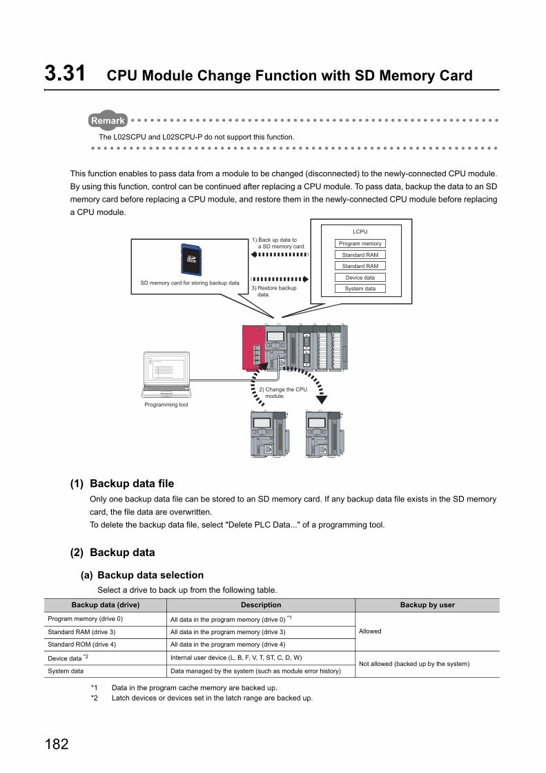
3.31 CPU Module Change Function with SD Memory Card
Remark
The L02SCPU and L02SCPU-P do not support this function.
This function enables to pass data from a module to be changed (disconnected) to the newly-connected CPU module.
By using this function, control can be continued after replacing a CPU module. To pass data, backup the data to an SD
memory card before replacing a CPU module, and restore them in the newly-connected CPU module before replacing
a CPU module.
(1) Backup data fileOnly one backup data file can be stored to an SD memory card. If any backup data file exists in the SD memory
card, the file data are overwritten.
To delete the backup data file, select "Delete PLC Data..." of a programming tool.
(2) Backup data
(a) Backup data selection
Select a drive to back up from the following table.
*1 Data in the program cache memory are backed up.*2 Latch devices or devices set in the latch range are backed up.
Backup data (drive) Description Backup by user
Program memory (drive 0) All data in the program memory (drive 0) *1
AllowedStandard RAM (drive 3) All data in the program memory (drive 3)
Standard ROM (drive 4) All data in the program memory (drive 4)
Device data *2 Internal user device (L, B, F, V, T, ST, C, D, W)Not allowed (backed up by the system)
System data Data managed by the system (such as module error history)
Programming tool
Standard RAM
Standard RAM
SD memory card for storing backup data
2) Change the CPU module.
3) Restore backup data.
1) Back up data to a SD memory card.
LCPU
Program memory
Device data
System data
182

CHAPTER 3 CPU MODULE FUNCTIONS
3
3.3
1 C
PU
Mo
du
le C
ha
ng
e F
un
ction
with
SD
Me
mo
ry Ca
rd
(b) Maximum backup data size
The following shows the maximum backup data size.
(Unit: K byte)
The backup data size can be checked by the following.
• "Create Backup Data for PLC Module Change" dialog box ( Page 189, Section 3.31.1 (2) (b))
• SD698 and SD699*1
*1 Available after starting backup.
Backup target data (drive) L02CPU, L02CPU-P L06CPU, L06CPU-P
L26CPU, L26CPU-P,
L26CPU-BT, L26CPU-
PBT
Program memory (drive 0) 82 244 1048
Standard RAM (drive 3) 130 770 770
Standard ROM (drive 4) 516 1032 2056
Device data 128 128 128
System data 53 76 76
Total (maximum) 909 2250 4078
183

3.31.1 Backup to SD memory card
This function can save data in the CPU module to an SD memory card. If an SD memory card is used in a running
system, data can be backed up by replacing the SD memory card with the one for storing a backup data.
(1) Procedure
*1 After preparation for backup is completed, the following functions are disabled. (They are not resumed after backup.) Refresh of a network module Refresh of CC-Link IE Field Network Basic Auto refresh of intelligent function module Simple PLC communication function
*2 Do not perform the following during backup. Insertion and removal of an SD memory card Power-off Reset
Start
Before backup start
Backup start setup request
from a programming toolThe backup start setup
contact is turned on.
Backup start prepared
Backup is ready to start.*1
Backup start preparation completed
Backup start request
from a programming tool
The backup start contact
is turned on.
Backup in execution*2
Backup to the SD memory card is completed.
Backup completed
End
Backup failed.
Backup error
Back up data again.
184

CHAPTER 3 CPU MODULE FUNCTIONS
3
3.3
1 C
PU
Mo
du
le C
ha
ng
e F
un
ction
with
SD
Me
mo
ry Ca
rd3
.31
.1 B
acku
p to
SD
me
mo
ry card
Backup status can be checked in SD690.
(a) Insertion and removal of SD memory card
An SD memory card can be inserted/removed after preparation for backup is completed.
(b) Operating status of the CPU module
To backup, the CPU module must be in the STOP status. (When the CPU module is either in the RUN or
PAUSE status, it is switched to the STOP status after the END processing where a request to backup start
preparation was received.)
After replacing the CPU module, it must be powered off and then on or reset. (Failure to do so keeps the CPU
module in the STOP status even after setting the switch to the RUN position.)
*1 The status includes a stop error.
SD690 value Status Description
0H Before backup start Backup is not started
1H Backup start prepared An SD memory card can be inserted/removed
2H Backup start preparation completed Set data to backup
3H Backup in execution Backup is in execution
4H Backup completed Backup has been completed
FFH Backup error Backup has failed due to an error
CPU operating status
Backup start setup is requested from a programming tool or the backup
start setup contact is turned on.
Backup start is requested from a programming tool or the backup
start contact is turned on.
Before backup start Backup start prepared Backup start preparation completed Backup in execution Backup completed
RUN/STOP*1
/PAUSESTOP*1
185

(2) Execution methodThe following two ways are available for backing up data to SD memory card.
• By contacts
• By remote operation
(a) Execution by contacts
Backup is executed by turning on the device specified in the "PLC Module Change Setting" dialog box.
Project window [Parameter] [PLC Parameter] [PLC System] [PLC Module Change
Setting]
*1 The CPU module enters the STOP status at the rise of the backup start setup contact, the backup start contact cannot be turned on in the program.
*2 The backup start setup contact and backup start contact cannot be set to the same device.*3 This indicates the default number of points. The setting range when the internal user device is set to the maximum
number of points (60K points) is M (0 to 61439) and B (0 to 0EFFF).*4 If data to be backed up is deselected in "Backup Target Data", only device data and system data are backed up.*5 Title is used for identifying backup data. Settings for the title of the backup data stored in an SD memory card can be
checked on the "Online Data Operation" dialog box with the "Delete" radio button selected.
Item Description Setting range Default
Backup Start Setup Contact *1At the rise of the selected device, backup is
ready to start.Applicable device *2
• X (0 to 1FFF)
• M (0 to 8191) *3
• B (0 to 1FFF) *3
Backup Start ContactAt the rise of the selected device, backup
enters execution status.
Backup Target Data Select the data to backup.*4• Program memory (drive 0)
• Standard RAM (drive 3)
• Standard ROM (drive 4)
All drives are backed up.
Format memory card before
backup
Select whether to format the SD memory card
before backup.
Format
Not formatNot format
Title Setting*5Set a title to append to the backup data stored
in the SD memory card.32 characters
Current time is set.
(Example) If data are backed up at
12 p.m. on October 1, 2008,
"20081001200" is set.
186

CHAPTER 3 CPU MODULE FUNCTIONS
3
3.3
1 C
PU
Mo
du
le C
ha
ng
e F
un
ction
with
SD
Me
mo
ry Ca
rd3
.31
.1 B
acku
p to
SD
me
mo
ry card
Turn on the backup start setup contact and then the backup start contact. Data are not backed up when only
the backup start contact is on.
*6 Since SM691 (Backup start preparation status flag) is on, data can be backed up again by turning off and then on the backup start contact.
Turn on the backup start setup contact.
Preparation for backup:1) Set the CPU module to the STOP status.2) Set the SD memory card so that the card can be removed from the CPU module.
1) Check that the preparation for backup is completed by the following methods. Check the LEDs. Check the special relay and special register. (a) SM691 is on. (b) SD690 stores 2h.2) Remove the SD memory card.3) Install a SD memory card for storing backup data.4) Turn on the backup start contact.
Back up data.
Check that the backup is completed by the following methods. Check the LEDs. Check the special relay and special register. (a) SM691 is on. (b) SD690 stores 4h.
Check for backup error*6. Check the LEDs. Check the special relay and special register. (a) SM691 is on. (b) SD690 stores FFh. (c) SD689 stores an error cause.
: Operation by the CPU module
: Operation by the user
187

If the backup start contact is turned on while the value in SD690 is 0H (Before backup start) or 1H (Backup start
prepared), data are not backed up. If the backup start contact is on before the value in SD690 becomes 2H
(Backup start preparation completed), turning off and then on the backup start contact again while the value in
SD690 is 2H (Backup start preparation completed) starts backup.
ON
OFF
OFF
ON
0 1 2 3 4
OFF
ON
Backup start setup is requested from a programming tool or the backup
start setup contact is turned on.
Backup start is requested from a programming tool or the backup
start contact is turned on.
Before backup start Backup start preparedBackup start
preparation completed Backup in execution Backup completed
Backup start setup contact
SM691 (Backup start preparation status flag)
Backup start contact
SD690 (Backup status)
188

CHAPTER 3 CPU MODULE FUNCTIONS
3
3.3
1 C
PU
Mo
du
le C
ha
ng
e F
un
ction
with
SD
Me
mo
ry Ca
rd3
.31
.1 B
acku
p to
SD
me
mo
ry card
(b) Execution by remote operation
Open the "Create Backup Data for PLC Module Change" dialog box.
[Online] [PLC Module Change] [Create Backup Data...]
Clicking the button displays the backup data size. (A value appears regardless of the CPU module connection status and SD memory card insertion status.) Data size can be checked only when the backup operation was executed by a remote operation.
(3) LEDs indicating backup statusBackup operation status can be checked by LED indication as shown below.
SD690 value Backup status LED indication
2HBackup start preparation
completedMODE: Flash (green), BAT.: Flash (yellow)
3H Backup in execution
The color changes as follows at intervals of 800ms.
1) MODE: Flash (green), BAT.: On (green)
2) MODE: Flash (green), BAT.: On (green), USER: On (red)
3) MODE: Flash (green), USER: On (red)
4H Backup completed MODE: Flash (green), BAT.: Flash (green)
FFH Backup error MODE: Flash (green), BAT.: Flash (green), USER: Flash (red)
189
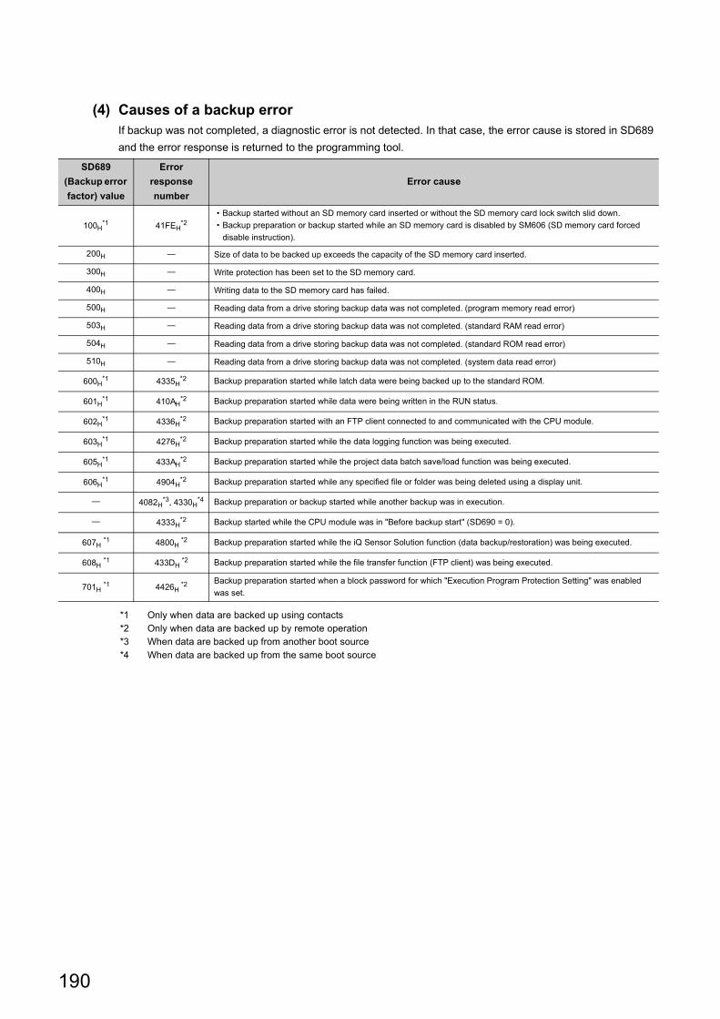
(4) Causes of a backup errorIf backup was not completed, a diagnostic error is not detected. In that case, the error cause is stored in SD689
and the error response is returned to the programming tool.
*1 Only when data are backed up using contacts*2 Only when data are backed up by remote operation*3 When data are backed up from another boot source*4 When data are backed up from the same boot source
SD689
(Backup error
factor) value
Error
response
number
Error cause
100H*1 41FEH
*2• Backup started without an SD memory card inserted or without the SD memory card lock switch slid down.
• Backup preparation or backup started while an SD memory card is disabled by SM606 (SD memory card forced
disable instruction).
200H Size of data to be backed up exceeds the capacity of the SD memory card inserted.
300H Write protection has been set to the SD memory card.
400H Writing data to the SD memory card has failed.
500H Reading data from a drive storing backup data was not completed. (program memory read error)
503H Reading data from a drive storing backup data was not completed. (standard RAM read error)
504H Reading data from a drive storing backup data was not completed. (standard ROM read error)
510H Reading data from a drive storing backup data was not completed. (system data read error)
600H*1 4335H
*2 Backup preparation started while latch data were being backed up to the standard ROM.
601H*1 410AH
*2 Backup preparation started while data were being written in the RUN status.
602H*1 4336H
*2 Backup preparation started with an FTP client connected to and communicated with the CPU module.
603H*1 4276H
*2 Backup preparation started while the data logging function was being executed.
605H*1 433AH
*2 Backup preparation started while the project data batch save/load function was being executed.
606H*1 4904H
*2 Backup preparation started while any specified file or folder was being deleted using a display unit.
4082H*3, 4330H
*4 Backup preparation or backup started while another backup was in execution.
4333H*2 Backup started while the CPU module was in "Before backup start" (SD690 = 0).
607H *1 4800H *2 Backup preparation started while the iQ Sensor Solution function (data backup/restoration) was being executed.
608H *1 433DH *2 Backup preparation started while the file transfer function (FTP client) was being executed.
701H *1 4426H *2 Backup preparation started when a block password for which "Execution Program Protection Setting" was enabled
was set.
190

CHAPTER 3 CPU MODULE FUNCTIONS
3
3.3
1 C
PU
Mo
du
le C
ha
ng
e F
un
ction
with
SD
Me
mo
ry Ca
rd3
.31
.1 B
acku
p to
SD
me
mo
ry card
(5) Functions that cannot be performed during backupThe following functions cannot be executed during backup.
(6) Precautions
(a) During data logging
Backup operation cannot be performed during data logging. To perform backup, stop the data logging. For how
to stop data logging, refer to the following.
QnUDVCPU/LCPU User's Manual (Data Logging Function)
Category Function Category Function
Drive operation
Format PLC memory
Online change
Online change (ladder mode)
Program memory batch download Online change (files)
Arrange PLC memory Online change (multiple blocks)
File operation
Write to PLC Change TC setting
Delete PLC data Trace Sampling trace registration
Write PLC user data Data logging Data logging registration
Delete PLC user data Remote operation Remote latch clear
File password 32 SM/SD operationLatch clear by using the special relay and special
register areas
Latch data backup Monitor Monitor condition setup
FTP function For all operations and commands Device test Executional conditioned device test
191

3.31.2 Backup data restoration
This function restores backup data in an SD memory card to the CPU module.
(1) Procedure
*1 Once a restoration is started, the following functions are stopped. (They are not resumed after restoration.) Refresh of a network module Refresh of CC-Link IE Field Network Basic Auto refresh of intelligent function module Simple PLC communication function
*2 Do not perform the following operations during restoration. Inserting or removing an SD memory card Power-off Reset
After restoration is completed, SM692 turns on.
• Restoration by remote operation • Automatic restoration
Status Description SD693 value
Before restoration start Restoration is not performed. 0H
Restoration in execution Restoration is in execution. 1H
Restoration completed Restoration is completed. 2H
Restoration error Restoration failed due to an error. FFH
Start
1: Before restoration start
Insert the SD memory card storing
the backup data to the CPU module
and restore the data with a
programming tool.
2: Restoration in execution*2
Restoration is completed.
3: Restoration completed
End
After restoration, power off
and then on or reset the CPU module.
Restoration is suspended.
4: Restoration error
Restoration failed.
Restoration is
performed again.
Start*1
End
1: Before restoration start
Insert the SD memory card storing the backup
data to the CPU module and power off and then
on or reset the CPU module.
2: Restoration in execution*2
Restoration is completed.
3: Restoration completed4: Restoration error
Restoration failed.
Restoration is
performed again.
After restoration, the CPU module
can continue operation.
Powering off and then on the CPU module
or resetting the CPU module is not necessary.
OFF
ONSM692
(Restoration
complete flag)
Before restoration
start
Restoration in
execution
Restoration
completed
192

CHAPTER 3 CPU MODULE FUNCTIONS
3
3.3
1 C
PU
Mo
du
le C
ha
ng
e F
un
ction
with
SD
Me
mo
ry Ca
rd3
.31
.2 B
acku
p d
ata
resto
ratio
n
(2) Execution methodThe following two methods are available for restoring backup data.
• Remote operation
• Automatic restoration
(a) Execution by remote operation
Open the "Restoration execution from backup data" dialog box.
[Online] [PLC Module Change] [Restore...]
To validate restored data, click "Yes" in the screen that appears after clicking the button in the
above dialog box and then power on or reset the CPU module.
(b) Execution by automatic restoration
On the "CPU Module Change Setting" dialog box, select "Auto restore at turn OFF -> ON or reset". ( Page
186, Section 3.31.1 (2) (a))
After backup, turn off and then on or reset the CPU module so that restoration starts. Restoration timing can be
set from either once at the first time or every time.
Option setting itemTurn on from off or reset of the CPU module
First time Second time or later
Restore for the first time only Restoration executed Restoration not executed (Operate as a standard SD memory card)
Restore every time Restoration executed Restoration executed
193

(3) LEDs indicating restoration statusRestoring status can be checked by LED indication as shown below.
(4) Causes of a restoration errorIf restoration was not completed, a diagnostic error is not detected. In that case, the error cause is stored in
SD692 and the error response is returned to the programming tool.
*1 Only when data are restored by remote operation.
If automatic restoration was not completed, "RESTORE ERROR" (error code: 2225 to 2227) occurs.
SD693 value Restoration status LED indication
0H Before restoration start MODE: On (green)
1H Restoration in execution
The color changes at intervals of 800ms as follows.
1) MODE: Flash (orange), BAT.: On (green)
2) MODE: Flash (orange), BAT.: On (green), USER: On (red)
3) MODE: Flash (orange), USER: On (red)
2H Restoration completed• By remote operationMODE: Flash (orange), BAT.: Flash (green)
• By automatic restorationMODE: On (green)
FFH Restoration error• By remote operationMODE: Flash (orange), BAT.: Flash (green), USER: Flash (red)
• By automatic restorationMODE: On (green), ERR.: Flash (red)
SD692 valueError response
numberError cause
800H The CPU module where data are restored is different model from the one where the backup source data are stored.
801H • Backup data files do not match.
• Reading of backup data from an SD memory card was not completed.
810H Writing of backup data to the restoration destination drive was not completed.
4335H*1 Restoration started while latch data were being backed up to the standard ROM.
410AH*1 Restoration started while data were being written in the RUN status.
4276H*1 Restoration started during data logging.
4336H*1 Restoration started with an FTP client connected to and communicated with the CPU module.
4330H*1 Restoration started during another restoration.
433AH*1 Restoration started while the project data batch save/load function was being executed.
4904H*1 Restoration started while any specified file or folder was being deleted using a display unit.
41FEH*1 • Restoration started without an SD memory card inserted or without the SD memory card lock switch slid down.
• Restoration started while an SD memory card is disabled by SM606 (SD memory card forced disable instruction).
4800H *1 Restoration started while the iQ Sensor Solution function (data backup/restoration) was being executed.
433DH*1 Restoration started while the file transfer function (FTP client) was being executed.
Error code Error message Error cause
2225
RESTORE ERROR
The CPU module where data are restored is different model from the one where the backup source data are
stored.
2226
• Backup data file is corrupt (The contents of backup data file do not match with the check code).
• Reading of backup data from an SD memory card was not completed.
• The SRAM card has been write-protected so that "Restore for the first time only" setting can not take
effect.
2227 Writing of backup data to the restoration destination drive was not completed.
194

CHAPTER 3 CPU MODULE FUNCTIONS
3
3.3
1 C
PU
Mo
du
le C
ha
ng
e F
un
ction
with
SD
Me
mo
ry Ca
rd3
.31
.2 B
acku
p d
ata
resto
ratio
n
(5) Functions that cannot be performed during restorationFunctions that cannot be performed during restoration are the same as those cannot be performed during
backup.
( Page 191, Section 3.31.1 (5))
(6) Precautions
(a) When boot settings are configured
If any parameter in the SD memory card has been set for booting, the data are overwritten according to the
boot setting even restoration is executed.
(b) When file password 32 is configured
Even if a file in the CPU module is protected by password 32, restoration continues.
(c) Combination of CPU modules for restoration
If the model of the CPU module where data is restored is different from the model of the CPU module where
backup data is stored, Restoration error occurs. However, using the CPU modules of the following
combinations allows completion of backup and restoration.
• L02CPU and L02CPU-P
• L06CPU and L06CPU-P
• L26CPU and L26CPU-P
• L26CPU-BT and L26CPU-PBT
195

3.32 Clock Function
This function is used for clock data management, such as storing a date into the error history, by reading internal clock
data of the CPU module. Clock data are retained the battery of a CPU module even after power-off or a momentary
power failure is occurred exceeding the allowable period of time.
(1) Clock data details
*1 Storing in SD213 for the first two digits and SD210 for the last two digits of the year.*2 Use only the expansion clock data read (S(P).DATERD) to read.
MELSEC-Q/L Programming Manual (Common Instruction)
(2) Changing clock dataTo change clock data, use any of the following.
• Programming tool
• SM and SD
• Program
• Clock setting of the display unit
(a) Programming tool
Open the "Set Clock" dialog box.
[Online] [Set Clock...]
(b) Clock setting of the display unit
Clock data can be set and checked in the display unit. ( Page 263, Section 4.3.1)
Clock data Description
Year Four digits*1 (from 1980 to 2079)
Month 1 to 12
Day 1 to 31 (Automatic leap year detection)
Hour 0 to 23 (24 hours)
Minute 0 to 59
Second 0 to 59
Day of the week 0: Sunday, 1: Monday, 2: Tuesday, 3: Wednesday, 4: Thursday, 5: Friday, 6: Saturday
1/1000sec *2 0 to 999
196

CHAPTER 3 CPU MODULE FUNCTIONS
3
3.3
2 C
lock F
un
ction
(c) SM and SD
Store clock data in SD210 to SD213. After the END processing for the scan where SM210 (Clock data set
request) were turned on from off, write the values stored in SD210 to SD213 to the CPU module.
(d) Program
Use an instruction to write clock data (DATEWR).
MELSEC-Q/L Programming Manual (Common Instruction)
● After changing clock data, a 1/1000 is reset to 0.
● Year data that can be set with GX Works2 is up to 2037.
(3) Clock data readTo read clock data, use either of the following.
• Program
• SM and SD
(a) Program
Use either of the following instructions. ( MELSEC-Q/L Programming Manual (Common Instruction))
• Clock data read (DATERD)
• Expansion clock data read (S(P).DATERD)
(b) SM and SD
The data are read out into SD210 to SD213 in a BCD value when SM213 (clock data read request) is turned
on.
(4) Precautions
(a) Initial clock data setting
Set the correct clock data because it has not been set when shipping.
(b) Correcting clock data
Whenever any part of the clock data are changed, the entire clock data must be written to the CPU module
again.
(c) Clock data range
When changing clock data, write data within the range given (3) in this section. If data outside the clock range
is written to the CPU module, the clock function does not operate correctly. However, errors do not occur if the
value is within the following range.
ExampleWrite operation to the CPU
moduleCPU module operation
February 30 Performed No error is detected.
Day 32 of month 13 Not performed• Upon DATEWR instruction: "OPERATION ERROR" (error code: 4100)
• Upon turn-on of SM210: SM211 (Clock data error) turns on
197

3.33 Battery Life-Prolonging Function
This function extends battery life of the CPU module by limiting data to retain by a battery to clock data only. The use of
this function initializes all data other than the clock data when the CPU module is powered off or is reset.
(1) Setting procedureEnter 0001H under Switch3 in the "Switch Setting for I/O and Intelligent Function Module" dialog box.
Project window [Parameter] [PLC Parameter] [I/O Assignment] [Switch Setting]
For the life of battery installed in the CPU module when the battery life-prolonging function is used, refer to the
following.
MELSEC-L CPU Module User's Manual (Hardware Design, Maintenance and Inspection)
Data retained by a battery Description
Error history The number of error history data are initialized to zero.
Latch relay (L) Cleared to zero.
Device in the latch range Cleared to zero.
Files in the standard RAMFiles are deleted. (Files are created again at power-on or reset.)
Data are cleared to zero.
198

CHAPTER 3 CPU MODULE FUNCTIONS
3
3.3
4 M
em
ory C
he
ck Fu
nctio
n
3.34 Memory Check Function
This function checks that data in the memories of the CPU module are not changed due to such as excessive electric
noise. Since the CPU module automatically checks a memory, setting for enabling this function is unnecessary. This
function does not require processing time.
(1) Data to be checked
(a) Program
The program during execution is compared with the user program written to the program memory. If they do not
match, a stop error, "RAM ERROR" (error code: 1160) is detected.
(b) Parameter
The parameters are compared with the ones written to the parameter-valid drive.
(c) Device memory
If the change of data in the device memory is detected, a stop error, "RAM ERROR" (error code: 1161) is
detected. For the LCPU whose serial number (first five digits) is "14012" or later, the device information, which
contains data change information, can be checked in SD927 and SD928. For details on the special register,
refer to the following.
MELSEC-L CPU Module User's Manual (Hardware Design, Maintenance and Inspection)
(2) Execution timing• Program: At program execution
• Parameter: When the CPU module is powered off and on, when the CPU module is reset, and when the
CPU module is set from STOP to RUN after data are written to it
• Device memory: When device data are read
199

3.35 Program Cache Memory Auto Recovery Function
This function is to restore the error location automatically by using data in the program memory, which are stored in the
flash ROM, when the memory check function ( Page 199, Section 3.34) detects an error in the program cache
memory. This function enables the CPU module to continue its operation even if an error such as change of data in the
program cache memory occurs due to noise.
Remark
Before executing this function, check the version of the CPU module used. ( Page 376, Appendix 2)
(1) Execution conditionThe function is executed when the following conditions are all met.
• The CPU module is in RUN status.
• Data in the program memory match those in the program cache memory.
Note that the function is not executed in the following conditions and RAM ERROR (error code: 1160) is detected
even though the above conditions are met:
• The change of data in the program cache memory was detected while the following operations were being
performed with the CPU module during RUN.
: The auto recovery processing is performed and no error occurs. : An error occurs depending on the condition. : An error occurs.
*1 If the change of data is detected while data in the program cache memory are being transferred to the program memory (while the following window is being displayed on the programming tool), the auto recovery processing is not performed and an error occurs.
• The change of data in the program cache memory was detected by SFC program.
• The change of data in the program cache memory was detected by the dedicated instruction such as the
S(P). instruction.
• The change of data in the program cache memory was detected by the rise instruction or the fall instruction.
• The data in the program cache memory was not restored due to the failure of the memory.
Operation itemLCPU with a serial number (first five digits) of "13102" or
later
Online change (ladder mode) *1
Password registration (program files)
Program memory batch download *1
Export to ROM format
Write to PLC (device comments) *1
200

CHAPTER 3 CPU MODULE FUNCTIONS
3
3.3
5 P
rog
ram
Ca
che
Me
mo
ry Au
to R
eco
very F
un
ction
To match the data in the program memory and those in the program cache memory, configure the setting to transfer the data
of the program cache memory to the program memory from "Options" screen.* 2 ( Page 157, Section 3.22.3 (5))
[Tool] [Options]
*2 The transferring of the data in the program cache memory to the program memory is set by default.
Other than the above, you can also use "Program Memory Batch Download" to match the data in the program memory and those in the program cache memory.
(2) Execution timingThe execution timing of this function is described below.
• When the program is executed
• When data are verified or data are read from the programmable controller
• When any one of the write operations listed under (1) in this section is performed*1
*1 To perform the auto recovery processing when a write operation is performed, use GX Works2 with version 1.80J or later. (GX Works2 must be used to perform the auto recovery processing at this timing because LCPU does not support GX Developer.)
201

3.36 Project Data Batch Save/Load Function
This function saves data in the CPU module to an SD memory card, and also reads the data saved in an SD memory
card to the CPU module.
This function enables users to read/write data (such as program file and parameter file) without using a personal
computer.
Remark
Before executing this function, check the version of the CPU module used. ( Page 376, Appendix 2)The L02SCPU and L02SCPU-P do not support this function.
Data (such as program file and device data) in
the CPU module can be saved or loaded using
a display unit.
2) Data with the CPU module information is sent.
1) Data are saved to the SD memory card.
5) Data are read from the SD memory card.
3) The CPU module information in the received data is edited for GX Works2.
4) The edited data is sent back to the SD memory card.
The saved data can be edited
remotely.
Multiple folders can be created according
to data. Saving dataProgram memory
CPU module
Inside the CPU module
Standard RAM
Standard ROMLoading data
SaveLoad folder
Data in the program memory
Data in the standard ROM
Data in the standard RAM
Data in the SD memory card
Device data
System file
Device data
SD memory card
SD memory card
SD memory card
LCPU
202

CHAPTER 3 CPU MODULE FUNCTIONS
3
3.3
6 P
roje
ct Da
ta B
atch
Sa
ve/L
oa
d F
un
ction
3.3
6.1
Ba
tch sa
ve
3.36.1 Batch save
This function saves data (such as program file and parameter file) in the CPU module to an SD memory card using a
display unit.
(1) Execution methodThe function can be executed using a display unit. For the operating method of the display unit, refer to
Page 280, Section 4.7.3.
(2) Folders to be usedWhen the function is executed, a new folder will be created under the "SaveLoad" folder within the root directory.
If there is no "SaveLoad" folder, it will be created upon execution of the function.
The "SaveLoad" folder can store up to 100 folders.
(a) Folder name
The created folder is automatically named as follows.
Remark
The range of the number at the end of the folder name is 00 to 99. The smallest number available will be assigned automatically. For example, if two folders, "20120401_00" and "20120401_02", have already existed and the batch save function is executed on April 2, 2012, the name of the new folder will be "20120402_01".
YYYYMMDD_**
Serial number (00 to 99)
Saved date (2 digits)
Saved month (2 digits)
Saved year (4 digits)
203

(b) Folder structure
The following shows the folder structure in the SD memory card.
(3) Target drives and data
(a) Target drives
The following drives are targeted.
• Drive 0 (program memory)*1
• Drive 2 (SD memory card)*2
• Drive 3 (standard RAM)
• Drive 4 (standard ROM)
*1 Data in the program cache memory are targeted.*2 Files only within the root directory are targeted. (Note that the data logging setting file in the "LOGGING" folder is
regarded as a target file.)
20120401_00
MAIN.QPG
PARAM.QPA
SVLDINF.QSL
/ SaveLoad
20120401_01
MAIN.QPG
PARAM.QPA
SVLDINF.QSL
Save folder
Save folder
Batch save/load target data
Batch save/load target data
204

CHAPTER 3 CPU MODULE FUNCTIONS
3
3.3
6 P
roje
ct Da
ta B
atch
Sa
ve/L
oa
d F
un
ction
3.3
6.1
Ba
tch sa
ve
(b) Target data
The following table lists save-target data.
: Saved, : Not saved
*1 All device data set in the Device tab of the PLC parameter dialog box*2 This file type is not saved when a block password for which "Execution Program Protection Setting" is enabled has been
set.
Up to 1024 files (all drives in total) can be saved with the batch save function.If more than 1024 files are targeted, an error occurs.When an error is detected, check the number of files in Drive 2 (SD memory card).
File typeFile name and extension (any given
name for ***)Save status
Parameter PARAM.QPA
Intelligent function module parameter IPARAM.QPA
Program*2 ***.QPG
Device comment ***.QCD
Initial device value ***.QDI
File register ***.QDR
Local device ***.QDL
Sampling trace file ***.QTD
PLC user data ***.CSV/BIN
Symbolic information ***.C32
Drive heading QN.DAT
Device data storage file DEVSTORE.QST
Module error collection file IERRLOG.QIE
Data logging setting file LOGCOM.QLG, LOG01 to LOG10.QLG
Data logging file ***.CSV
Menu definition file MENUDEF.QDF
Predefined protocol setting file ECPRTCL.QPT,CPRTCL.QPT
Latch data backup file LCHDAT00.QBK
Backup file (for data backup to an SD memory card) MEMBKUP0.QBP
Device data file*1 DEVDATA.QDT
205

(4) Batch save statusThe batch save status can be checked in SD635 (Project data batch save status).
(5) Causes of a batch save errorWhen the batch save processing has failed, a diagnostic error is not detected. An error message is displayed on
the display unit and the error cause is stored in SD634 (Project data batch save error cause).
*1 The number of save-target system files (up to five files) and its size (up to 10KB) are included.*2 If the function is executed again and the same error occurs, the possible cause is a hardware failure of the CPU module
or SD memory card. Please consult your local Mitsubishi representative.
SD635 value Batch save status Description
0H Batch save not executed The batch save function is not executed.
1H Batch save being executed The batch save function is being executed.
2H Batch save completed The batch save processing is completed successfully.
FFH Batch save error The batch save processing has failed and an error occurs.
SD634 value Description
100H• An SD memory card is not inserted.
• The SD memory card lock switch of the CPU module is not slid down.
101H Use of an SD memory card is disabled by SM606 (SD memory card forced disable instruction).
200H• Size of data to be batch-saved exceeds the capacity of the SD memory card.*1
• The number of files to be batch-saved exceeds the number of storable files of the SD memory card.*1
201H The number of files to be batch-saved exceeds 1024.
202H More than 100 folders exist in the "SaveLoad" folder.
300H The SD memory card is write-protected.
400H Writing data to the SD memory card has failed.*2
401H The SD memory card was removed during the batch save processing.
500H Reading data from the target drive (program memory) has failed.*2
503H Reading data from the target drive (standard RAM) has failed.*2
504H Reading data from the target drive (standard ROM) has failed.*2
505H Reading data from the target drive (SD memory card) has failed.*2
510H Reading data from the target drive (system data) has failed.*2
600H The batch save function was executed during the latch data backup to the standard ROM.
601H The batch save function was executed during online change.
602H The batch save function was executed with an FTP client connected to and communicated with the CPU module.
604HThe batch save function was executed while the CPU module change function with SD memory card was being
executed.
607HThe batch save function was executed while the iQ Sensor Solution function (data backup/restoration) was being
executed.
608H The batch save function was executed while the file transfer function (FTP client) was being executed.
701HThe batch save function was executed for the program for which a block password was set and "Execution Program
Protection Setting" of the password was enabled.
206

CHAPTER 3 CPU MODULE FUNCTIONS
3
3.3
6 P
roje
ct Da
ta B
atch
Sa
ve/L
oa
d F
un
ction
3.3
6.1
Ba
tch sa
ve
(6) Precautions
(a) Precautions for executing the function simultaneously with another function
• The batch save function cannot be executed while any of the following function is being executed. If
executed, an error occurs.
• Latch data backup to standard ROM
• Online change (Writing programs in RUN status)
• File transfer function (FTP server)
• File transfer function (FTP client)
• CPU module change function with SD memory card
• iQ Sensor Solution function (data backup/restoration)
• If the batch save function is executed while the data logging function is being executed, the sampling
performance of the data logging function degrades. This may lead to data missing or increase the frequency
of data missing.
(b) Precautions during execution
• Do not power off or reset the CPU module, or do not insert or remove the SD memory card while the function
is being executed. The processing stops and project data cannot be saved properly.
• If save-target data are added or modified using a programming tool while the function is being executed, the
saved data may differ from the original data or data inconsistency may occur. To prevent this, do not add or
modify save-target data while the function is being executed. Also, set the operating status of the CPU
module to STOP, and execute the batch save function.
• If the batch save function is executed when the CPU module is in STOP status, the following functions are
suspended. After data are saved successfully, the functions automatically restart.
• Refresh of a network module
• Refresh of CC-Link IE Field Network Basic
• Auto refresh of an intelligent function module
• Simple PLC communication function (read/write)
• The following online functions cannot be executed during the batch save processing. If executed, an error
response is returned to the request source.
(c) Predefined protocol setting file
If the communication protocol setting files are stored in Drive 2 (SD memory card) and Drive 4 (standard ROM),
only the file stored in Drive 2 (SD memory card) is targeted for batch save.
When executing the batch save function, store the communication protocol setting file in the valid drive only.
Category Function Category Function
Drive operation
Format PLC memory
Online change
Online change (ladder mode)
Clear PLC memory (Clear all file registers) Online change (multiple blocks)
Write title Change TC setting
Program memory batch download Online change (files)
Arrange PLC memory Trace Sampling trace registration
File operation
Write to PLC Data logging Data logging registration
Delete PLC data Remote operation Remote latch clear
Write PLC user data SM/SD operationLatch clear by using the special relay and special
register areas
Delete PLC user data Monitor Monitor condition setup
Password registration Device test Executional conditioned device test
Latch data backup to standard ROM
Others
CPU module change function with SD memory card
File transfer
function (FTP
server)
For all operations and commands Register/cancel display unit menu
207

(7) Editing dataData saved in the SD memory card by the batch save function can be edited using a programming tool before the
data are loaded.
For the editing method, refer to the following.
Manual for the programming tool used
● When reading data from the SD memory card to a personal computer to edit the saved program file, read the parameter file together.
● Any file that has been added to the SD memory card without using a programming tool cannot be loaded.
(a) Data that are not editable
The following data cannot be edited using a programming tool.
• PLC user data
• Latch data backup file
• Backup file (for data backup to an SD memory card)
• Data logging setting file
208

CHAPTER 3 CPU MODULE FUNCTIONS
3
3.3
6 P
roje
ct Da
ta B
atch
Sa
ve/L
oa
d F
un
ction
3.3
6.2
Ba
tch lo
ad
3.36.2 Batch load
This function reads the data saved in an SD memory card to the CPU module.
The following two methods are available to execute the function.
• Batch load using a display unit
• Auto loading using the special register (SD909)
(1) Execution timing
(a) Batch load using a display unit
The function is executed when the operation is performed on the display unit.
(b) Auto loading using SD909
The function is executed when:
• the CPU module is powered off and on
• the CPU module is reset
(2) Batch load target folders
(a) Batch load using a display unit
Folders under the "SaveLoad" folder in the SD memory card are targeted.
The name of these folders can be customized within 48 one-byte (24 two-byte) characters.
If the number of characters for the name exceeds 48 (or 24), the file will be excluded from the load target.
(b) Auto loading using SD909
Folders named "AutoLoad**"*1 under the "SaveLoad" folder in the SD memory card are targeted.
*1 When the folder number is specified at "**" within the range between 01 and 99, the desired folder can be loaded.Folders can also be loaded automatically without specifying the folder number.
For the target folder structure and target data, refer to the following.• Folder structure: Page 204, Section 3.36.1 (2) (b)• Target data: Page 204, Section 3.36.1 (3)
209

(3) ProcedureFor the execution procedure using a display unit, refer to Page 281, Section 4.7.4.
For auto loading, set a desired folder number in SD909 (Auto loading target folder number).
To execute auto loading without specifying the folder number, set 0 (default) in SD909. (The load target folder
name is "AutoLoad".)
The auto loading procedures for each case are described below.
(a) When the folder number is not specified
1. Save data into the SD memory card by the batch save function of a display unit or using GX
Works2.
2. Change the name of the saved data folder to "AutoLoad" using a personal computer.
3. Power off and on or reset the CPU module.
4. Data in the "AutoLoad" folder are automatically loaded to the CPU module.
● Auto loading cannot be performed if the SD memory card is write-protected.Remove write protection from the SD memory card, and execute auto loading.
● When the "AutoLoad" folder exists, data in the folder are automatically loaded whenever the CPU module is powered off and on or is reset.To prevent this, change the folder name.
● When 0 (default) is set in SD909 and no "AutoLoad" folder exists, an error does not occur. This is because the CPU module determines that auto loading is disabled.
● If any folder or file (including read-only files) with the same name exists in the load-destination CPU module, data in the corresponding folder or file will be overwritten.
(b) When the folder number is specified
1. Save data into the SD memory card by the batch save function of a display unit or using GX
Works2.
2. Change the name of the saved data folder to "AutoLoad**" using a personal computer.
Specify any number between 01 and 99 at "**".
3. Set the number assigned in Step 2 in SD909.
For example, when the folder name is "AutoLoad01", set "1" in SD909.
4. Power off and on or reset the CPU module.
5. Data in the specified folder are automatically loaded to the CPU module.
● Auto loading cannot be performed if the SD memory card is write-protected.Remove write protection from the SD memory card, and execute auto loading.
● The value in SD909 returns to 0 (default) upon completion of auto loading.If the "AutoLoad" folder exists even after completion of auto loading, data in the folder will be automatically loaded again when the CPU module is powered off and on or is reset next time.
● If any folder or file (including read-only files) with the same name exists in the load-destination CPU module, data in the corresponding folder or file will be overwritten.
210

CHAPTER 3 CPU MODULE FUNCTIONS
3
3.3
6 P
roje
ct Da
ta B
atch
Sa
ve/L
oa
d F
un
ction
3.3
6.2
Ba
tch lo
ad
(4) Operation when the file password 32 is setThe following table shows the load availability when the file password 32 is set to the load-source or load-
destination file.
: Loaded, : Not Loaded
*1 If the file password 32s are set to more than one file, the passwords of all files have to be the same.Even one file has a different password, files cannot be loaded.
(5) Batch load statusThe batch load status can be checked in SD637 (Project data batch load status).
In the case of auto loading, the status can also be checked with LED indication.
Password of load-
source file
Load-destination filePassword match Load availability
Existence Password
SetExist
SetMatched*1
Not matched
Not set
Not exist
Not setExist
Set
Not set
Not exist
SD637
value
Batch load
statusDescription LED indication
0HBatch load not
executed
The batch load function is not
executed.MODE: On (green)
1HBatch load being
executed
The batch load function is being
executed.
The LED indication changes as follows at intervals of 800ms.
1) MODE: Flashing (orange), BAT.: On (green)
2) MODE: Flashing (orange), BAT.: On (green), USER: On (red)
3) MODE: Flashing (orange), USER: On (red)
2HBatch load
completed
The batch load processing is
completed successfully.MODE: On (green)
FFH Batch load errorThe batch load processing has failed
and an error occurs.MODE: On (green), ERR.: Flashing (red)
211

(6) Causes of a batch load errorWhen the batch load processing has failed, the error cause is stored in SD636 (Project data batch load error
cause).
When the batch load function is executed using a display unit, an error message is displayed on the display unit.
*1 If the function is executed again and the same error occurs, the possible cause is a hardware failure of the CPU module or SD memory card. Please consult your local Mitsubishi representative.
SD636 value Description
800H The model of the load-destination CPU module is different from that of the load-source CPU module.
801H Reading data from the SD memory card has failed.*1
802H The SD memory card was removed during batch load processing.
803H A data folder without a system file (SVLDINF.QSL) was loaded.
804H• The file password 32 of the load-destination file is different from that of the load-source file.
• A file password 32 is not set to the load-source file while the load-destination file has a password.
805H
• When the folder number (1 to 99) is set in SD909 (Auto loading target folder number) for auto loading, the folder with
the corresponding number does not exist in the SD memory card.
• The folder number out of the setting range (other than 0 to 99) is set in SD909 (Auto loading target folder number).
810H Loading data to the load-destination drive has failed.*1
820H Loading of the folder that includes a file that may be used in another application has failed.
821H Format was executed while any file that may be used in another application existed.
900H
• When the batch load function is executed, the SD memory card is not inserted.
• When the batch load function is executed, the SD memory card lock switch of the CPU module is not slid down.
• When the folder number (1 to 99) is set in SD909 (Auto loading target folder number) for auto loading, the SD
memory card is not inserted.
• When the folder number (1 to 99) is set in SD909 (Auto loading target folder number) for auto loading, the SD
memory card lock switch of the CPU module is not slid down.
901H Use of an SD memory card is disabled by SM606 (SD memory card forced disable instruction).
A00H
• The size of load-target data is larger than the free space of each drive in the CPU module or SD memory card.
• The number of files to be loaded exceeds the number of files can be stored in each drive in the CPU module or SD
memory card.
B00H The SD memory card is write-protected.
C00H The batch load function was executed using a display unit during the latch data backup to the standard ROM.
C01H The batch load function was executed using a display unit during online change.
C02HThe batch load function was executed using a display unit with an FTP client connected to and communicated with the
CPU module.
C04HThe batch load function was executed using a display unit while the CPU module change function with SD memory
card was being executed.
C07HThe batch load function was executed while the iQ Sensor Solution function (data backup/restoration) was being
executed.
C08H The batch load function was executed while the file transfer function (FTP client) was being executed.
C10H The batch load function was executed using a display unit when the CPU module was in RUN or PAUSE status.
212

CHAPTER 3 CPU MODULE FUNCTIONS
3
3.3
6 P
roje
ct Da
ta B
atch
Sa
ve/L
oa
d F
un
ction
3.3
6.2
Ba
tch lo
ad
When the auto loading processing has failed, "LOAD ERROR" (error code: 2240 to 2248) occurs.
(7) Precautions
(a) Precautions for selecting CPU module models
If the model of the load destination CPU module is different from that of the load source CPU module, the batch
load function cannot be executed. However, the batch load function can complete normally in the following
combinations of CPU modules.
• L02CPU and L02CPU-P
• L06CPU and L06CPU-P
• L26CPU and L26CPU-P
• L26CPU-BT and L26CPU-PBT
(b) Precautions for executing the function simultaneously with another function
• If data are saved into the SD memory card while the sampling trace function is being executed, the load-
destination CPU module may misunderstand that a request is from a different source when trace
start/suspension or trigger execution is requested. An alarm message is displayed at this time. However,
there is no impact on the operation of the sampling trace function.
• The batch load function cannot be executed while any of the following function is being executed. If
executed, an error occurs.
• Latch data backup to standard ROM
• Online change (Writing programs in RUN status)
• File transfer function (FTP server)
• File transfer function (FTP client)
• CPU module change function with SD memory card
• iQ Sensor Solution function (data backup/restoration)
• Do not set auto loading simultaneously with the following functions. If set, auto loading is not executed.
• Boot operation
• Data restoration by the CPU module change function with SD memory card*1
• Latch data backup to standard ROM
*1 This applies only when automatic restoration is set.
Error code Error message Error cause
2240
LOAD ERROR
The model of the load-destination CPU module is different from that of the load-source CPU module.
2241 Reading data from the SD memory card has failed.
2242 A system file (SVLDINF.QSL) does not exist in the load-target folder.
2243The file password 32 of the load-destination file is different from that of the load-source file. Or, a file
password 32 is not set to the load-source file while the load-destination file has a password.
2244
• When the folder number (1 to 99) is set in SD909 (Auto loading target folder number), a folder with the
corresponding number does not exist in the SD memory card.
• The folder number out of the setting range (other than 0 to 99) is set in SD909 (Auto loading target folder
number).
2245 Loading data to the load-destination drive has failed.
2246
• When the folder number (1 to 99) is set in SD909 (Auto loading target folder number), the SD memory card
is not inserted.
• When the folder number (1 to 99) is set in SD909 (Auto loading target folder number), the SD memory card
lock switch of the CPU module is not slid down.
2247
• The size of load-target data is larger than the capacity of the CPU module memory or SD memory card.
• The number of files to be loaded exceeds the number of files can be stored in the CPU module or SD
memory card.
2248 Auto loading was executed with the SD memory card write-protected.
213

(c) Precautions for editing data
• If a file in the load-target folder is deleted, the function corresponding to the deleted file cannot continue the
same execution status after data are loaded.
• If a system file (SVLDINF.QSL) in a data folder is deleted, the corresponding folder cannot be loaded. Do not
delete the system file of the load target folder.
(d) Precautions for parameter settings
• If the batch load function is executed without formatting Drive 0 (program memory) of the load-destination
CPU module, the setting that has been configured originally to the load-destination CPU module is used for
the "High Speed Monitor Area from Other Station" parameter on the Boot File tab of the PLC parameter
dialog box.
(e) Precautions during execution
• Do not power off or reset the CPU module while the function is being executed. If performed, the processing
stops and data cannot be loaded properly.
• If the batch load function is executed using a display unit, the following functions are suspended. After data
are loaded successfully, the functions automatically restart.
• Refresh of a network module
• Refresh of CC-Link IE Field Network Basic
• Auto refresh of an intelligent function module
• Simple PLC communication function (read/write)
• Even if the RUN/STOP/RESET switch of the CPU module is switched from STOP to RUN, or the remote
RUN or remote PAUSE function is executed while the function is being executed, the operating status of the
CPU module remains in STOP. If the operating status is changed during the batch load processing, the
status changes after the processing is completed.
• If the CPU module detects any file that may be used in another application during the batch load processing,
an error occurs at the following timing or due to the following reason.
• Timing: while drives are being formatted (if the format is executed)
• Reason: files other than the one in use are loaded
• The online functions that cannot be executed during the batch load processing are the same as those that
cannot be executed during the batch save processing. ( Page 207, Section 3.36.1 (6) (b))
214

CHAPTER 3 CPU MODULE FUNCTIONS
3
3.3
7 P
red
efin
ed
Pro
toco
l Fu
nctio
n3
.37
.1 C
om
mu
nica
tion
s via E
the
rne
t
3.37 Predefined Protocol Function
This function sends and receives packets predefined by using GX Works2, enabling easy communications with
external devices (such as measuring instruments and bar code readers).
Data are sent and received by registering the protocol setting data to the CPU module, and executing the program for
starting data communications. Use of the function helps to reduce the significant number of program steps since no
program is required to communicate with external devices.
In addition, the CPU module can send and receive data that vary in each communication as well as fixed data (such as
numerical values and codes) since devices can be included in the communication packets.
Remark
Before executing this function, check the version of the CPU module used. ( Page 376, Appendix 2)
3.37.1 Communications via Ethernet
The CPU module communicates with external devices via the built-in Ethernet ports.
For details on communications via Ethernet, refer to the following.
MELSEC-L CPU Module User's Manual (Built-In Ethernet Function)
215

3.37.2 Communications via RS-232 and RS-422/485
The CPU module communicates with external devices via the RS-232 interface of the CPU module, RS-232 adapter,
or RS-422/485 adapter.
Set protocols required for data communications with external devices using the predefined protocol support function of
GX Works2.
Protocols can be either selected from the predefined protocol library, or created and edited by users.
Remark
The CPU module with the RS-232 interface and the LCPU where the RS-232 adapter or RS-422/485 adapter can be mounted support this function. ( Page 376, Appendix 2)
Set values are in the Send data storage area.
Protocol No.1 is specified.
Protocol is executed.
Normal completion flag ON
Error completion flag ON
Error code is stored.
CPRTCLexecutioncommand
Predefinedprotocolready
CR Data
Send
ENQ
STX Data CR
1) Setting protocolsProtocols can be set easily using the predefined protocol support function of GX Works2.
2) Writing protocolsThe set protocols are written to the CPU module.
3) Executing protocolsExecute protocols by dedicated instructions.One dedicated instruction can execute multiple protocols.
Receive
Data communication becomes possible with the protocol corresponding to each connected device.
216

CHAPTER 3 CPU MODULE FUNCTIONS
3
3.3
7 P
red
efin
ed
Pro
toco
l Fu
nctio
n3
.37
.2 C
om
mu
nica
tion
s via R
S-2
32
an
d R
S-4
22
/48
5
(1) Specifications
(a) Transmission specifications
The following table lists the transmission specifications.
(b) Functional specifications
The following table lists the functional specifications.
*1 Number of protocols specified as the protocol setting data*2 Total number of packets set to each protocol*3 Size as a sum of all packets
Item Specifications
Communication method Full-duplex communication
Synchronization method Asynchronous method
Transmission speed
RS-232 interface of CPU module, RS-232
adapter
9600bps, 19200bps, 38400bps, 57600bps,
115200bps
RS-422/485 adapter1200bps, 2400bps, 4800bps, 9600bps, 19200bps,
38400bps, 57600bps, 115200bps
Data format
Start bit 1
Data bit• 7
• 8
Parity bit• Available
• Not available
Stop bit• 1
• 2
Error detection
Parity check
• Available (Select odd or even number in
parameter.)
• Not available
Sumcheck
• Available (Determine whether to use sumcheck
codes and check method according to the
protocol used.)
• Not available
Line configuration
(connection)
RS-232 interface of CPU module, RS-232
adapter1:1
RS-422/485 adapter 1:1, 1:n, n:1, m:n
Line configuration (data
communication)
RS-232 interface of CPU module, RS-232
adapter1:1
RS-422/485 adapter 1:1, n:1
Item Specifications
Protocol setting data
Number of protocols*1 Up to 128
Number of packets*2 Up to 256
Packet area data size*3 Up to 12288 bytes
Available channel CH1 (fixed)
Protocol execution method S(P).CPRTCL instruction
Length of data that can be sent or received at a time Up to 2048 bytes
217

(2) Setting methodThe setting required for using the predefined protocol function is described below.
1. Open the "Predefined Protocol Support Function"
screen.
[Tool] [Predefined Protocol Support Function]
[Built-in/Adapter Serial]
2. Create a new file.
[File] [New] "Add"
3. In the "Add Protocol" screen, select "Predefined
Protocol Library" or "Add New".
When "Predefined Protocol Library" is selected, select a
desired protocol from the library registered in GX
Works2.
Select "User Protocol Library" in the "Add Protocol" screen to read the protocol stored by the user. For details on the user protocol library, refer to the following.GX Works2 Version 1 Operating Manual (Intelligent Function Module)
218

CHAPTER 3 CPU MODULE FUNCTIONS
3
3.3
7 P
red
efin
ed
Pro
toco
l Fu
nctio
n3
.37
.2 C
om
mu
nica
tion
s via R
S-2
32
an
d R
S-4
22
/48
5
4. Set the items required for data communications.
In the "Protocol Detailed Setting" screen, set the
communication parameters for the protocol.
"Protocol Setting" screenSelect protocol
[Edit] [Protocol Detailed Setting]
5. Set the packet configuration.
In the "Packet Setting" screen, set the configuration of
the packet to be sent or received.
"Protocol Setting" screen"Variable unset" or
"Element unset"
219

6. Write the protocol setting data to the CPU module.
In the "Writing Protocol Setting" screen, specify the
write-target drive in the CPU module and write the
protocol setting data.*1
[Module Read/Write] [Write to Module]
*1 The written protocol setting data will be enabled when• the CPU module is powered on or is reset, or• SM1333 (Predefined protocol setting check request) is turned on.
● To enable the written protocol setting data without powering off or resetting the CPU module, turn on SM1333 (Predefined protocol setting check request). Before enabling the protocol setting data, stop the CPU module and check that no instruction is being executed. Depending on the on-timing of SM1333, the instruction being executed may end abnormally.
7. Set the PLC parameters.
Set "Predefined Protocol" to the "Select Function"
parameter on the "Adapter Serial Setting" tab or "Built-in
Serial Setting" tab.
"PLC Parameter Setting" screen"Adapter Serial
Setting" or "Built-in Serial Setting"
8. Create a program for starting data communications.
Use the S(P).CPRTCL instruction.
220

CHAPTER 3 CPU MODULE FUNCTIONS
3
3.3
7 P
red
efin
ed
Pro
toco
l Fu
nctio
n3
.37
.2 C
om
mu
nica
tion
s via R
S-2
32
an
d R
S-4
22
/48
5
For the protocol setting method, refer to the following.
GX Works2 Version 1 Operating Manual (Intelligent Function Module)
9. Write the program to the CPU module.
[Online] [Write to PLC]
10. Execute the program written to the CPU module by
using the S(P).CPRTCL instruction.
221

(3) Setting items of the predefined protocol support function
(a) Communication type
There are three protocol communication types: "Send", "Receive", and "Send & Receive".
For details on the protocol communication types, refer to the following.
MELSEC-L Serial Communication Module User's Manual (Basic)
(b) Packet elements set for "Packet Setting"
The packet elements include "Header", "Terminator", "Length", "Static Data", "Non-conversion Variable",
"Conversion Variable", "Check Code", and "Non-verified Reception".
Up to 32 elements can be set in a single packet.
The protocol setting method and packet elements are the same as those for the serial communication module,
except for some differences. ( MELSEC-L Serial Communication Module User's Manual (Basic))
The following are the differences.
• Read the C24 (serial communication module) as the CPU module in the manual.
• Buffer memory cannot be set as a data storage area for conversion variables and non-conversion
variables.
222

CHAPTER 3 CPU MODULE FUNCTIONS
3
3.3
7 P
red
efin
ed
Pro
toco
l Fu
nctio
n3
.37
.2 C
om
mu
nica
tion
s via R
S-2
32
an
d R
S-4
22
/48
5
(4) Setting items of "Adapter Serial Setting" or "Built-in Serial Setting"Setting items of "Adapter Serial Setting" or "Built-in Serial Setting", (items required for data communications using
the predefined protocol function) are described below. For other setting items, refer to the following.
Page 353, Appendix 1.2
(a) Select function
Select "Predefined Protocol".
(b) Predefined protocol support function (Device to store predefined protocol operation
status)
Set the start device for storing the predefined protocol operating status. The following information is stored in
the area of three words starting from the selected device.
*1 Even after data communications using the predefined protocol function (executed by the S(P).CPRTCL instruction) is completed, the stored values are held.
Device for storing
the predefined
protocol operating
status (offset)
Item Description*1 Default
+0 Protocol cancellation
The protocol cancellation request status is stored.
0: No cancellation requested
1: Cancellation requested (set by users)
2: Cancellation completed (set by the CPU module)
0+1Protocol execution
status
The execution status of the predefined protocol function is
stored.
0: Not executed
1: Waiting for data to be sent
2: Data being sent
3: Waiting for data to be received
4: Data being received
5: Execution completed
+2Number of protocol
executions
The number of protocol executions is stored.
0: No execution
1 to 65535: Number of executions (The value remains the
same after 65535.)
223

(5) S(P).CPRTCL instructionThis instruction sends and receives packets set by the predefined protocol support function of GX Works2.
Usage of the S(P).CPRTCL instruction is the same as that of the G(P).CPRTCL instruction for the serial
communication module, except for some differences. For the G(P).CPRTCL instruction, refer to the following.
MELSEC-L Serial Communication Module User's Manual (Basic)
The following are the differences.
(6) Execution conditionsThe predefined protocol function can be executed when the protocol setting data is enabled and SM1332
(Predefined protocol ready) is on. The written protocol setting data will be enabled when
• the CPU module is powered on or is reset, or
• SM1333 (Predefined protocol setting check request) is turned on.
SM1332 is used as an interlock signal to execute the protocol.
(a) Operation of SM1332
SM1332 (Predefined protocol ready) turns on when the protocol setting data is normal, and remains off when
the protocol setting data is abnormal or not written.
If the protocol setting data is abnormal, the following occurs.
• The error details are stored in SD1337 to SD1340 (Predefined protocol setting data error information).
• The error code is stored in SD1351 (Predefined protocol function error code).
Registration of the protocol setting data can be checked in the following special register areas.
• SD1341 (Number of protocols registered)
• SD1342 to SD1349 (Protocol registration status)
(b) Changing the protocol setting data without powering off or resetting the CPU
module
The protocol setting data can be changed by turning on SM1333 (Predefined protocol setting check request).
After SM1333 turns on, the following occurs.
• SM1332 (Predefined protocol ready) turns off.
• If the protocol setting data is normal, SM1332 turns on, and SM1333 turns off.
• If the protocol setting data is abnormal, SM1332 does not turn on, and SM1333 turns off. The error
information is stored in SD1337 to SD1340 (Predefined protocol setting data error information) and
SD1351 (Predefined protocol function error code).
Item Difference
Setting data Un
U0 (dummy) needs to be specified.
Since this is a dummy, no change is required when replacing from the
G(P).CPRTCL instruction of the serial communication module.
Setting data n1 Setting data n1 is fixed to "1: Channel 1 (CH1 side)".
Cancellation of protocol execution
Protocol execution can be cancelled by using the device for storing the predefined
protocol operating status (offset+0) set in the "Adapter Serial Setting" or "Built-in
Serial Setting" tab of the PLC parameter dialog box, instead of the buffer memory.
Functional protocolThe predefined protocol function of the CPU module does not support the
functional protocol.
224

CHAPTER 3 CPU MODULE FUNCTIONS
3
3.3
7 P
red
efin
ed
Pro
toco
l Fu
nctio
n3
.37
.2 C
om
mu
nica
tion
s via R
S-2
32
an
d R
S-4
22
/48
5
(7) Enabling/disabling echo back of RS-422/485 adapterWhen data are communicated via RS-485 (two-wire type) in the RS-422/485 adapter, the sent data can be
echoed back to the RDA and RDB of own station.
The echo back status (receiving the sent data or not (discard the data)) can be specified.
(a) Setting method
1. Turn on SM1334 (RS-422/485 echo back specification). (Disable echo back.)
2. The CPU module starts sending data.
(b) Precautions
• The setting of SM1334 (RS-422/485 echo back specification) is enabled when a send request is received.
Even if the setting is changed during the send processing, the change is not reflected to the operation.
• SM1334 can be set only when the RS-422/485 adapter is used.
SDA
SDB
RDA
RDB
SDA
SDB
RDA
RDB
Target deviceSending data
Receives or not receive(discards) the data.
RS-422/485adapter
225

(8) Operation image and data structure of the predefined protocol functionFor operation image and data structure of the predefined protocol function, refer to the following. (Read the C24
(serial communication module) as the CPU module.)
MELSEC-L Serial Communication Module User's Manual (Basic)
(9) Precautions
(a) To use two predefined protocol functions simultaneously (Ethernet or RS-
232/422/485)
Store the predefined protocol setting files in the same drive. If the setting files are stored separately in the SD
memory card and the standard ROM, the setting stored in the SD memory card is enabled while the setting
stored in the standard ROM is disabled.
To enable the predefined protocol setting stored in the standard ROM, format the SD memory card or delete
the predefined protocol setting stored in the SD memory card. Then, enable the setting.
The predefined protocol setting can be checked and deleted by operating the PLC user data.
[Online] [PLC User Data] [Read] or [Delete]
(b) After writing the predefined protocol setting
Power on or reset the CPU module, or turn on SM1333 (Predefined protocol setting check request) to enable
the written protocol setting data. If the written data are not enabled, the data may be changed unintentionally
when the CPU module is powered on or is reset.
(c) Device data
Data set by the predefined protocol function are communicated during the service processing. Therefore, if the
COM instruction is executed while b15 of SD778 (Refresh processing selection when the COM/CCOM
instruction is executed) is on, data communications are also performed at the execution of the COM instruction.
(d) S(P).CPRTCL instruction
Even though the instruction has been completed successfully, an error code may be stored in SD1351
(Predefined protocol function error code). If data communications fail even though the instruction has been
completed successfully, check SD1351 and take corrective actions.
The following are the error codes that may be stored.
• Overrun error (7F67H)
• Framing error (7F68H)
• Parity error (7F69H)
• Buffer full error (7F6AH)
(e) Time settings of the protocol detailed setting
Since the passage of time, such as receive wait time, standby time, and monitoring time, is checked during the
service processing, the set time may be exceeded depending on the scan time. Set the time values considering
the scan time.
226

CHAPTER 3 CPU MODULE FUNCTIONS
3
3.3
8 S
eria
l Co
mm
un
icatio
n F
un
ction
3.38 Serial Communication Function
This function communicates data using the MC protocol by connecting the RS-232 interface of the CPU module, the
RS-232 adapter, or the RS-422/485 adapter to the following devices.
• MC protocol-compatible devices
• Personal computer
• HMI from other companies
This section describes the specifications, settings, and details of the function.
Remark
The CPU module with the RS-232 interface and the LCPU where the RS-232 adapter or RS-422/485 adapter can be mounted support this function. ( Page 376, Appendix 2)
● A personal computer or an HMI from other companies can communicate only with a CPU module connected to it, the RS-232 adapter, and the RS-422/485 adapter. Communication with other stations in the network is not available.
● For details on MC protocol, refer to the following.MELSEC Communication Protocol Reference Manual
● The RS-422/485 adapter can be used to connect multiple external devices (multidrop connection).
Communication in the MC protocol
RS-232 cable
Personal computer or HMI
227

(1) Specifications
(a) Transmission specifications
The following table lists the transmission specifications used for the serial communication function. Check that
the specifications of the personal computer or HMI from other companies used match those in the following
table.
*1 The item is set in the PLC parameter of the programming tool. ( Page 370, Appendix 1.2 (13), Page 372, Appendix 1.2 (14))
*2 This control is performed only when data are communicated via RS-232.*3 Relationship between the MC protocol formats and frames is shown below.
: Available, : Not available
Item Setting range Default
Communication method Full-duplex communication
Synchronization method Asynchronous method
Transmission speed*1
• When RS-232 interface of CPU
module or RS-232 adapter is used:
9600bps, 19200bps, 38400bps,
57600bps, 115200bps
• When RS-422/485 adapter is used:
1200bps, 2400bps, 4800bps,
9600bps, 19200bps, 38400bps,
57600bps, 115200bps
19200bps
Data format
• Start bit: 1
• Data bit: 8
• Parity bit: Odd
• Stop bit: 1
MC protocol format*3 (auto
identification)
• Format 4 (ASCII)
• Format 5 (binary)
Frame*3 • QnA-compatible 3C frame
• QnA-compatible 4C frame
Transmission control DTR/DSR flow control*2
Sumcheck code*1 Include/Not include Include
Transmission wait time*1No wait time, 10 to 150ms (in increments
of 10ms)No wait time
Online change*1 Enable/Disable Disable
Overall cable distance 15m
Line configuration (connection, data
communication)
• When RS-232 interface of CPU
module or RS-232 adapter is used:
1:1
• When RS-422/485 adapter is used:
1:1, 1:n, n:1, m:n
Function Format 4 Format 5
Communication using ASCII
code
QnA-compatible 3C frame
QnA-compatible 4C frame
Communication using binary
codeQnA-compatible 4C frame
228

CHAPTER 3 CPU MODULE FUNCTIONS
3
3.3
8 S
eria
l Co
mm
un
icatio
n F
un
ction
(2) CommandsThe following table lists the MC protocol commands that can be executed.
*1 To perform online change, check the "Permit" checkbox under "Online Change".*2 Devices such as TS, TC, SS, SC, CS, and CC cannot be specified in units of words.
For the monitor registration, an error (4032H) occurs during the monitor operation.
*3 The monitor condition specification cannot be used for these commands.*4 Do not execute monitor registration from multiple external devices. If executed, the last monitor registration becomes
valid.*5 Set the number of processing points within the range of the following calculation formula.
(number of word access points) 12 + (number of double word access points) 14 960• One point of a bit device corresponds to 16 bits for word access or to 32 bits for double word access.• One point of a word device corresponds to one word for word access or to two words for double word access.
Function Command Description of processingNumber of
processing points
Device
memory
Batch read
In units of
bits0401 (001) Reads out a bit device in units of one point.
• ASCII: 3584 points
• BIN: 7168 points
In units of
words0401 (000)
Reads out a bit device in units of 16 points. 480 words (7680 points)
Reads out a word device in units of one point. 480 points
Batch write*1
In units of
bits1401 (001) Writes into a bit device in units of one point.
• ASCII: 3584 points
• BIN: 7168 points
In units of
words1401 (000)
Writes into a bit device in units of 16 points. 480 words (7680 points)
Writes into a word device in units of one point. 480 points
Random
read*2*3
In units of
words0403 (000)
Reads out a bit device in units of 16 or 32 points by
specifying a device/device number at random.
96 pointsReads out a word device in units of one or two
points by specifying a device/device number at
random.
Test*1 (random
write)
In units of
bits1402 (001)
Sets/resets a bit device in units of one point by
specifying a device/device number at random.94 points
In units of
words*21402 (000)
Sets/resets a bit device in units of 16 or 32 points
by specifying a device/device number at random.*5Writes into a word device in units of one or two
points by specifying a device/device number at
random.
Monitor
registration*2
*3*4
In units of
words0801 (000)
Registers a bit device to be monitored in units of 16
or 32 points.96 points
Registers a word device to be monitored in units of
one or two points.96 points
MonitorIn units of
words0802 (000) Monitors a device registered.
Number of monitor
registration points
229

(3) Accessible devicesThe following table lists accessible devices with the serial communication function.
*1 This is a code specified in MC protocol messages. When communicating data in ASCII code, specify the device code in two characters. If the code consists of only one character, add "*" (ASCII code: 2AH) or a space (ASCII code: 20H) after
the character.*2 Devices of DX/DY1000 or later are not available. Use X/Y devices to access devices of X/Y1000 or later.
Classification DeviceDevice code*1
Device number rangeASCII Binary
Internal system
device
Function input
(Cannot be accessed)
Hexadecimal
Function output Hexadecimal
Function register Decimal
Special relay SM 91H
Within the device number range of the
CPU module accessed.
Note, however, that local devices
cannot be accessed.
Decimal
Special register SD A9H Decimal
Internal user device
Input X * 9CH Hexadecimal
Output Y * 9DH Hexadecimal
Internal relay M * 90H Decimal
Latch relay L * 92H Decimal
Annunciator F * 93H Decimal
Edge relay V * 94H Decimal
Link relay B * A0H Hexadecimal
Data register D * A8H Decimal
Link register W * B4H Hexadecimal
Timer
Contact TS C1H
DecimalCoil TC C0H
Current value TN C2H
Retentive timer
Contact SS C7H
DecimalCoil SC C6H
Current value SN C8H
Counter
Contact CS C4H
DecimalCoil CC C3H
Current value CN C5H
Link special relay SB A1H Hexadecimal
Link special register SW B5H Hexadecimal
Step relay S * 98H Decimal
Direct input*2 DX A2H Hexadecimal
Direct output*2 DY A3H Hexadecimal
Index register Index register Z * CCH
Within the device number range of the
CPU module accessed
Decimal
File register File registerR * AFH Decimal
ZR B0H Decimal
Extended data
registerExtended data register D * A8H
• Binary: Within the device number
range of the CPU module accessed
• ASCII: 000000 to 999999 (up to
976.6K points)
Decimal
Extended link
registerExtended link register W * B4H
Specify within the device number
range of the access destination CPU
module.
Hexadecimal
230

CHAPTER 3 CPU MODULE FUNCTIONS
3
3.3
8 S
eria
l Co
mm
un
icatio
n F
un
ction
(4) Setting transmission specificationsSet the transmission specifications of the serial communication function in the "Built-in Serial Setting" or "Adapter
Serial Setting" tab of the PLC parameter dialog box. ( Page 353, Appendix 1.2)
• Set "Serial Communication" to the "Select Function" in the "Built-in Serial Setting" or "Adapter Serial Setting"
tab.
• Set the adapter type*1, sum check code, communication speed setting, station number setting*2,
transmission wait time, and online change status.
*1 The adapter type can be set only in the "Adapter Serial Setting" tab.*2 The station number can be set only when the RS-422/485 adapter is used.
231

(5) Precautions
(a) Switching a connection from an HMI from other companies to a programming tool
A connection device can be switched from a personal computer or an HMI from other companies to a
programming tool during communication. However, this operation causes a communication error in the
personal computer or HMI. For a startup method of the personal computer or HMI after it is reconnected to the
CPU module, refer to the manual for the device used.
(b) Transmission speed set in the Transfer setup screen
When "Use Serial Communication" is selected, the transmission speed set in the Transfer setup screen of the
programming tool is ignored.
(c) Communication error
If any of the following conditions is met, no response is returned (a communication error occurs). Take a
corrective action.
*1 When the "Sum Check" checkbox is selected, the sumcheck code is included.• The frame identification number of a frame to be sent is incorrect.• The number of transmission bytes is under the header part size.
• The serial communication function is set not to be used.
• Communication is made at different transmission speed and data format.
• A frame to be sent has no correct starting end or terminal.
3C frame format 4: ENQ/CR + LF
4C frame format 4: ENQ/CR + LF
4C frame format 5*1: DLE + STX/DLE + ETX
232

CHAPTER 3 CPU MODULE FUNCTIONS
3
3.3
8 S
eria
l Co
mm
un
icatio
n F
un
ction
(6) Error codes during communication with the serial communication functionThe following table lists the error codes (together with their descriptions and corrective actions) sent from the
CPU module to the external device when an error occurs during communication using the serial communication
function.
Error code
(hexadecimal)Error item Description Corrective action
4000H to 4FFFH Error detected by the CPU module (error occurred by
other than the serial communication function)
Refer to the following manual and take corrective
actions.
MELSEC-L CPU Module User's Manual (Hardware
Design, Maintenance and Inspection)
7155HUnregistered
monitor errorA monitor request was given before monitor registration.
Give a monitor request after registering a device to be
monitored.
7157HRequest target
specification error
A CPU module that does not support the serial
communication function is specified as a request target
module or is in the specified route.
Check that the transmission message is addressed to
the CPU module that supports the serial communication
function. If not, correct the address and restart
communication.
7164HRequest data
error
The requested data or device specification method is
wrong.
Check the sent message/requested data of the external
device, correct it, and restart communication.
7167HDisabled during
RUN
A write command was specified while online change is
disabled.
• Enable the online change and restart communication.
• Set the CPU module to STOP and restart
communication.
7E40H Command errorA command or a subcommand that does not exist is
specified.
Check and correct the sent message of the external
device, and restart communication.
7E41H Data length error
The number of points specified for random write/read
exceeds the number of points enabled for
communication.
Check and correct the sent message of the external
device, and restart communication.
7E42H Data count errorThe requested number of points exceeds the range of
the command.
Check and correct the sent message of the external
device, and restart communication.
7E43H Device errorThe device specified does not exist. The device specified
cannot be specified by the corresponding command.
Check and correct the sent message of the external
device, and restart communication.
7E47HContinuous
request error
The next request was received before the response
message was returned.
Do not give continuous requests from the external
device. Match the monitoring time of Timer 1 with the
time-out time of the external device.
7F21HReceive header
section error
The command (frame) section specified is in error.Check and correct the sent message of the external
device, and restart communication.The ASCII code received cannot be converted into
binary.
7F22H Command error The command or device specified does not exist.Check and correct the sent message of the external
device, and restart communication.
7F23HMC protocol
message error
The data (such as ETX and CR + LF) specified after the
character part does not exist or in error.
Check and correct the sent message of the external
device, and restart communication.
7F24H Sum check errorThe calculated sum check does not match the received
sum check.Review the sum check of the external device.
7F67H Overrun errorThe next data was received before the CPU module
completed receive processing.
Reduce the communication speed and restart
communication. Check the CUP module for a momentary
power failure. (For the CPU module, use the special
register SD53 to check.) When a momentary power
failure occurs, remove its cause.
7F68H Framing error
• The stop bit setting does not match.
• Communication line became unstable by powering
on/off the target device.
• Noise is generated on the communication line.
• Match the setting of the CPU module with that of the
external device.
• Take noise reduction measures.
7F69H Parity error
• The parity bit setting does not match.
• Communication line became unstable by powering
on/off the target device.
• Noise is generated on the communication line.
• Match the setting of the CPU module with that of the
external device.
• Take noise reduction measures.
233

3.39 iQ Sensor Solution Function
The iQ Sensor Solution function includes the following functions.
Remark
● Before using this function, check the versions of the CPU module and the programming tool used. ( Page 376, Appendix 2)
● The L02SCPU and L02SCPU-P do not support this function.
● For details on iQ Sensor Solution functions, refer to the following.iQ Sensor Solution Reference Manual
Function Description
Automatic detection of connected device
Detects devices supporting iQ Sensor Solution connected to the CPU
module, and automatically displays them on "List of devices" and "Device
map area" using a programming tool.
System configuration check
Compares the system configuration information displayed on a
programming tool with the actual system configuration, and checks if they
match.
Reflection of the communication setting
Reflects the communication settings (such as IP addresses) of devices
supporting iQ Sensor Solution on "Device map area" to the devices
connected over Ethernet in the system.
Sensor parameter read/write Reads/writes parameters from/to devices supporting iQ Sensor Solution.
Monitoring
Monitors the current values (such as measurement values and input/output
values), status (error existence), and error information of devices supporting
iQ Sensor Solution graphically using a programming tool.
Data backup/restoration
Backs up setting data (such as parameters) in devices supporting iQ Sensor
Solution to an SD memory card. The data backed up can be restored as
necessary.
234

CHAPTER 3 CPU MODULE FUNCTIONS
3
3.3
9 iQ
Se
nso
r So
lutio
n F
un
ction
Memo
235

CHAPTER 4 DISPLAY UNIT FUNCTIONS
A display unit is an LCD attachable to the CPU module. Using a display unit allows checking system status and
changing system setting values without software packages.
If an error occurs, the error cause can be determined by displaying the error information.
Remark
The L02SCPU and L02SCPU-P do not support the display unit functions.
(1) Description of the buttonsUnless otherwise specified, buttons on a display unit operate as follows.
Type Name Description
Up arrow button
Moves the cursor up, scrolls the screen up, and increases values. In the following screens,
pressing a device longer will increase a bit device value in increments of 10 bits (decimal
notation) or 16 bits (hexadecimal notation), and will increase a word device value in
increments of 10 words (decimal notation) or 16 words (hexadecimal notation).
• Device monitor/test
• Buffer memory monitor/test
Down arrow button
Moves the cursor down, scrolls the screen down, and decreases values. In the following
screens, pressing a device longer will increase a bit device value in increments of 10 bits
(decimal notation) or 16 bits (hexadecimal notation), and will increase a word device value
in increments of 10 words (decimal notation) or 16 words (hexadecimal notation).
• Device monitor/test
• Buffer memory monitor/test
Right arrow button Moves the cursor forward and switches screens.
Left arrow button Moves the cursor back and switches screens.
OK button Switches screens, executes functions, and accepts selection.
ESC button Returns the display to the previously displayed screen or the initial screen for each function.
Device monitor/test
Forced ON/OFF
Checking/changing the I/O status and settingvalues of intelligent function module
Error information/log display
Scan time display
OK
ESC
236

CHAPTER 4 DISPLAY UNIT FUNCTIONS
4
(2) Menu structureFunctions can be selected in the "function selection" screen.
In screen figures, the Japanese version is shown on the left and the English version on the right. Switch a
displayed language by language setting. ( Page 283, Section 4.8.1)
The menu structure is as shown below.
*1 Menus lower than the "initial setting change" screen depend on the selected module.
LOG
CPU MON/TEST
CPU SETTINGS
MOD MON/TEST
MOD SETTINGS
USER MESSAGE
OPTIONS
DEV MON/TEST
DEVICE CLEAR
FORCED ON/OFF
SCAN TIME MON
BLT-IN I/O MON
ERROR MONITOR
DEVICE MEMORY
FILE REGISTER
SET ON/OFF
CLR FORCE
CLR ALL FORCES
LIST FORCES
BLT-IN POSITION
BLT-IN COUNTER
BLT-IN ERR CLR
MONITOR
CLEAR
CLOCK SETTING
SPECIFY I/O No.
MODULE LIST
USER MSG DSP
LANGUAGE
CONTRAST
BACKLIGHT
POPUP POP BLK DISABLE
SPECIFY I/O No.
MODULE LIST
MEM CARD OP FILE LIST/DEL
FREE SPACE
BATCH SAVING
BATCH LOADING
USER MSG DSP
INIT CHANGE*1
237

(3) Standby screenThe standby screen is the initial screen of the display unit. The screen displays year, month, day, day of the week,
hour, minute, and second. The internal time of the CPU module is automatically read to the display unit. Pressing
any button moves you to the "function selection" screen.* 1
*1 The button is invalid.
(4) Backlight
(a) Normal status
The backlight lights up green. (When any button is not pressed within set lighting period, the backlight will turn
off.) The backlight will turn on again in the following cases.
• Any button is pressed.
• A user message is popped up.
• An error is detected from the display unit by the self-diagnostic function.*1
*1 If this occurs, the backlight will not turn off even after elapse of set period.
(b) Error status
If an error occurs in the CPU module, the backlight lights up red. (When any button is not pressed within set
lighting period, the backlight will turn off.) Check error information in the "Error list" screen and clear the error.
( Page 259, Section 4.2.6)
Note that the backlight status does not change in the following cases.
• "0" has been set to each cause number setting area of LED display priority ranking (SD207 to SD209).
• The ERR. LED, USER LED, or BAT. LED of the CPU module does not turn on.
(5) Self-diagnostic functionWhen a display unit detects an error by self-diagnostics, a continuation error ("DISPLAY ERROR") occurs in the
CPU module, and an error message "DISPLAY UNIT ERROR" is displayed on the display unit. If the same error
occurs even after the CPU module is reset, the possible cause is a hardware failure of the CPU module or the
display unit. Check a 4-digit error code displayed on the display unit, and please consult your local Mitsubishi
representative.
ESC
238

CHAPTER 4 DISPLAY UNIT FUNCTIONS
4
(6) Level navigationTo clear where you are, level navigation is displayed on the top of the screen. The level navigation is inverted and
the selected menu flashes.
Note that level navigation is not displayed in the detail setting screen of each function.
(7) ScrollingWhen the display screen consists of several pages, the title line is displayed. An arrow indicating a scrollable
direction is displayed on the top right of the screen.
However, when the contents of a screen with title line (such as a screen that displays an error message) can be
displayed at a time, the scroll symbol (arrow) will not be displayed.
Parent menu Current menu
Down scroll arrow
Up/down scroll arrow
Up scroll arrow
239

4.1 Function List
The following table lists the functions of a display unit.
Category Function nameDisplayed
function nameDescription Reference
CPU monitor/test
Device monitor/test DEV MON/TEST Monitors and tests device memory values.Page 241,
Section 4.2.1
Device
clear
Device memory clear DEVICE MEMORY Clears all device memory values.Page 249,
Section 4.2.2File register clear FILE REGISTERClears values of file register including extended
data register and extended link register.
Forced
on/off
Forced on/off registration SET ON/OFF Forcibly turns on or off devices X and Y.
Page 251,
Section 4.2.3
Forced on/off clear CLR FORCE Clears a forced on/off-registered device.
Forced on/off batch clear CLR ALL FORCES Clears all forced on/off-registered devices.
Forced on/off list LIST FORCES Lists forced on/off-registered devices.
Scan time monitor SCAN TIME MONDisplays the current value, maximum value,
and minimum value of scan time.
Page 254,
Section 4.2.4
Built-in I/O
function
monitor
Built-in positioning function
monitorBLT-IN POSITION
Displays the setting values of the built-in
positioning function.
Page 255,
Section 4.2.5
Built-in high-speed counter
function monitorBLT-IN COUNTER
Displays the setting values of the built-in high-
speed counter function.
Built-in I/O function error
clearBLT-IN ERR CLR Clears errors of the built-in I/O function.
Error
display
Current error monitor MONITOR
Displays the current error code, message,
common information, and individual
information. Page 259,
Section 4.2.6Error log display LOG Displays information of error logs.
Error clear CLEAR Clears continuation errors.
CPU settings Clock setting CLOCK SETTING Sets the internal time of the CPU module.Page 263,
Section 4.3
Module
monitor/testBuffer memory monitor/test BUF MEM MON/TES
Monitors and tests the buffer memory value of
the selected module.
Page 265,
Section 4.4
Module settings Initial setting change INIT CHANGE Sets the initial value of the selected module.Page 270,
Section 4.5
User message User message USER MESSAGEChecks a user message executed by the
UMSG instruction.
Page 273,
Section 4.6
Memory card
operation
File list/delete FILE LIST/DEL
Displays folders and files stored in an SD
memory card in a list, and deletes a specified
folder or file.
Page 274,
Section 4.7.1
Free space check FREE SPACE Displays the free space on an SD memory card.Page 279,
Section 4.7.2
Batch save BATCH SAVINGSaves data in the CPU module into an SD
memory card.
Page 280,
Section 4.7.3
Batch load BATCH LOADINGLoads data in an SD memory card to the CPU
module.
Page 281,
Section 4.7.4
OPTIONS
Language setting LANGUAGE Selects a displayed language.Page 283,
Section 4.8.1
Contrast adjustment CONTRAST Sets tone of displayed characters.Page 284,
Section 4.8.2
Lighting period setting BACKLIGHT Sets a period while the backlight is on.Page 285,
Section 4.8.3
Pop-up setting POP BLK DISABLE Enables pop-up display.Page 286,
Section 4.8.4
240
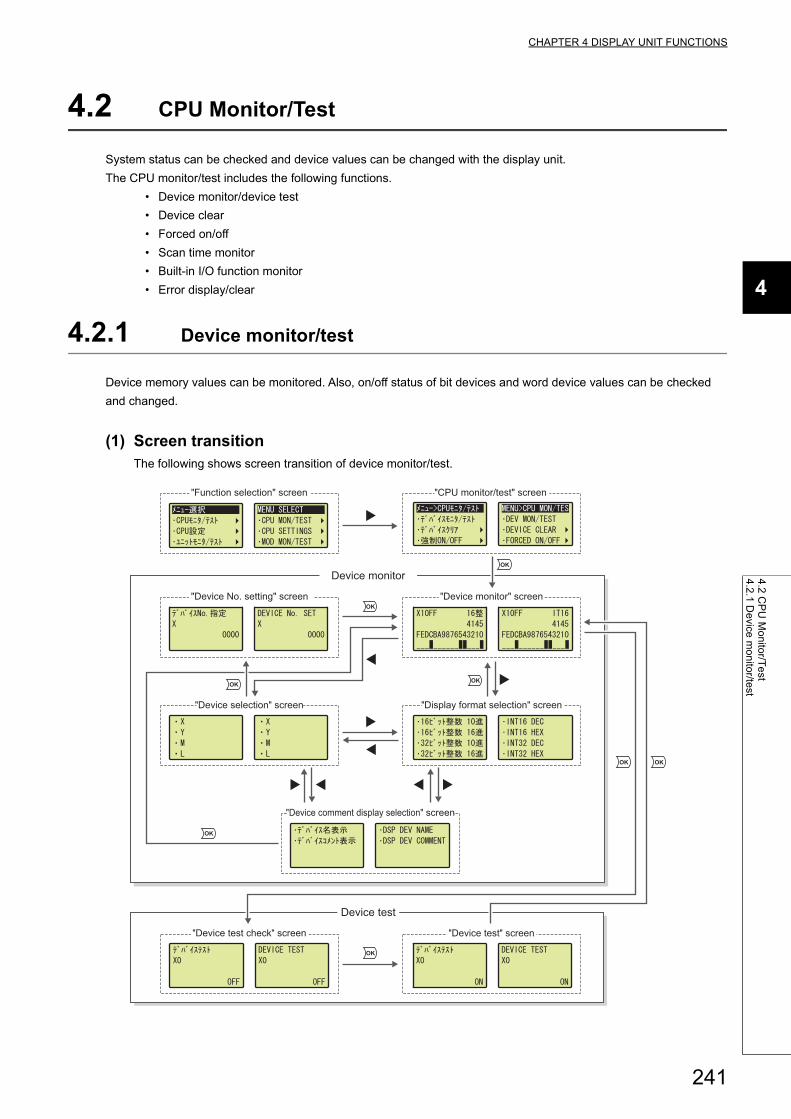
CHAPTER 4 DISPLAY UNIT FUNCTIONS
4
4.2
CP
U M
on
itor/T
est
4.2
.1 D
evice
mo
nito
r/test
4.2 CPU Monitor/Test
System status can be checked and device values can be changed with the display unit.
The CPU monitor/test includes the following functions.
• Device monitor/device test
• Device clear
• Forced on/off
• Scan time monitor
• Built-in I/O function monitor
• Error display/clear
4.2.1 Device monitor/test
Device memory values can be monitored. Also, on/off status of bit devices and word device values can be checked
and changed.
(1) Screen transitionThe following shows screen transition of device monitor/test.
OK
OK
OK
OK
OK
OK
OK
OK
"Function selection" screen
"Device No. setting" screen
Device monitor
Device test
"Device monitor" screen
"Device test check" screen
"Device selection" screen "Display format selection" screen
"Device comment display selection" screen
"Device test" screen
"CPU monitor/test" screen
241

(2) Devices that can be monitored/testedThe following shows devices that can be monitored and tested by device monitor/test. Note that local devices
cannot be monitored and tested.
*1 Digit-specified devices, devices specified by indirect specification, and bit-specified devices cannot be set.*2 Device test cannot be executed.
(3) Specifying a device to be monitored or testedPerform the following operation.
*1 The device number is displayed in decimal or hexadecimal, according to the notation of each device. Regardless of the notation, the device number is displayed with the number of digits that can be set.
Type Device*1
Bit device X, Y, M, L, B, F, SB, V, SM, T (contact, coil*2), ST (contact, coil*2), C (contact, coil*2)
Word deviceD, D (extended data register), W, W (extended link register), SW, SD, Z, R, ZR, T (current value), ST (current
value), C (current value)
"Device monitor" screen 1. Press the button.
"Device selection" screen 2. Select a target device using the and buttons
and press the button.
"Device No. setting" screen 3. Move the cursor using the and buttons,
increase or decrease a device number*1 using the
and buttons, and press the button.
OK
OK
242

CHAPTER 4 DISPLAY UNIT FUNCTIONS
4
4.2
CP
U M
on
itor/T
est
4.2
.1 D
evice
mo
nito
r/test
(4) Display formatThe following table shows display format available for device monitor/test.
*1 Device test cannot be executed while a value is displayed in real number. (except for bit device, timer (T), retentive timer (ST), and counter (C))
Also, a device number can be displayed with device comment. Note that, however, the device comment can be
displayed up to 5 two-byte characters (11 one-byte characters).
(a) Specifying display format
Perform the following operation.
FormatNumeric
valueBit display Remarks
16-bit integerDecimal
AvailableA sign is appended for negative values only.
Hexadecimal When a value is less than four digits, "0" is assigned for the remaining digits.
32-bit integerDecimal
Not available
A sign is appended for minus values only.
Hexadecimal When a value is less than eight digits, "0" is assigned for the remaining digits.
Real number (single
precision)*1
A value is displayed in floating point exponent (2 lines). A sign is appended
for negative values only.
Real number (double
precision)*1A value is displayed in floating point exponent (2 lines). A sign is appended
for negative values only.
"Device monitor" screen 1. Press the button.
"Display format selection" screen 2. Select display format using the and buttons
and press the button.OK
243

(b) Specifying a device comment
To display a device with device comment, perform the following operation.*1*2*3
*1 A device comment can be displayed only in the following screens. "Device monitor" screen "Device test check" screen "Device test" screen
*2 To display a device with device comment, preset "Comment File Used in a Command" in the PLC File tab of the PLC Parameter dialog box.
*3 The device comment can be displayed up to 5 two-byte characters (11 one-byte characters).
● If a device comment file is changed while the device comment is displayed, the device comment is updated when the screen transitions.
● When several device comment files are used, the device comment in the device comment file used when the screen changes to the "device monitor" screen is displayed.
"Device monitor" screen 1. Press the button twice.
"Device comment display selection" screen 2. Select "DSP DEV COMMENT" using the and
buttons and press the button.OK
244

CHAPTER 4 DISPLAY UNIT FUNCTIONS
4
4.2
CP
U M
on
itor/T
est
4.2
.1 D
evice
mo
nito
r/test
(5) Device monitorA device specified in (3) in this section can be monitored from the "device monitor" screen.
Depending on update timing of a screen, the update of a value displayed in the "device monitor" screen may delay accordingly.
(a) Monitoring a bit device (display format: 16-bit integer)
The specified device, and display format, a value, and bit status of the specified device can be monitored.
*1 When a bit device is specified within one word from the start number of the bit device, the specified device number will be changed to the start number.Example: X1 to XF X0
*2 When a bit device is specified within one word from the last number of the bit device, the specified device number will be changed to the last number.Example: X1FF1 to X1FFE X1FFF
*3 When X1 is specified as a monitor target, "F" indicates the on/off status of X10.
(b) Monitoring a word device (display format: 16-bit integer)
The specified device, and display format, a value, and bit status of the specified device can be monitored.
The device number can be changed by 1 word (16 bits)
with the *1 and *2 buttons.
Display format
Device valueBit position counted from
the specified device *3
On/off status of bits
ON :
OFF :
The device number can be changed by 1 word (16 bits)
with the and buttons.
Display format
Device valueBit position counted
from the first bit of the
specified device
On/off status of bits
ON :
OFF :
245

(c) Monitoring a bit device (display format: 32-bit integer)*1
The specified device, and display format and a value of the specified device can be monitored.
*1 Even if the display format is set to 32-bit integer (decimal) or 32-bit integer (hexadecimal), a bit device value is displayed in 16-bit integer (decimal) or 16-bit integer (hexadecimal).
(d) Monitoring a word device (display format: 32-bit integer)
The specified device, and display format and a value of the specified device can be monitored.
(e) Monitoring a real number (single precision)*2
The specified device, and display format and a value of the specified device can be monitored.
*1 If the device value is "-0", unnormalized number, nonnumeric character, or , "********" is displayed.*2 When a bit device is monitored, the device value is displayed in 16-bit integer (decimal).
The device number can be changed by 1 word (16 bits)
with the and buttons.
Display format
Device value
Bit position counted from
the specified device
On/off status of bits
ON :
OFF :
Display format
Device value
The device number can be changed by 1 word (16 bits)
with the and buttons.
Display format
Device value in exponent *1
The device number can be changed by 1 word (16 bits)
with the and buttons.
246

CHAPTER 4 DISPLAY UNIT FUNCTIONS
4
4.2
CP
U M
on
itor/T
est
4.2
.1 D
evice
mo
nito
r/test
(f) Monitoring a real number (double precision)*2
The specified device, and display format and a value of the specified device can be monitored.
*1 If the device value is "-0", unnormalized number, nonnumeric character, or , "********" is displayed.*2 When a bit device is monitored, the device value is displayed in 16-bit integer (decimal).
(g) Monitoring a bit device in decimal
The specified device and bit status of the specified device can be monitored. Regardless of display format, a
screen with the following style appears.
(h) Monitoring timer (T), retentive timer (ST), and counter (C)
The specified device and a value and bit status of the specified device can be monitored. The current value is
displayed in decimal or hexadecimal, the format specified in the "display format selection" screen. When
"REAL" has been specified, the current value is displayed in decimal.
Display format
Device value in exponent *1
The device number can be changed by 1 word (16 bits)
with the and buttons.
The device number can be changed by 10 bits
with the and buttons.
Display format and a device
value are not displayed.
The device number can be changed by1 word (16 bits)
with the and buttons.
Current value
Display format is not displayed.
Coil
Contact
On/off status of bits
ON :
OFF :
247

(6) Device testOn/off status of a bit device and a word device value can be changed.
"Device monitor" screen 1. Press the button.
"Device test check" screen 2. Select a device using the and buttons. (a
device value is changed by 1 bit for bit device and 1
word for word device) and press the button.
"Device test" screen 3. Change device status. Change on/off status of a bit
device using the and buttons. For a word
device, the cursor can be moved forward or back
using the and buttons. Increase or decrease
the value at the cursor position using the and
buttons.
4. Pressing the button will update the value to the
one set in device test.
OK
(Bit device)
(Word device)
(Timer (T), retentive timer (ST), and counter (C))
OK
(Bit device)
(Word device)
(Timer (T), retentive timer (ST), and counter (C))
OK
248

CHAPTER 4 DISPLAY UNIT FUNCTIONS
4
4.2
CP
U M
on
itor/T
est
4.2
.2 D
evice
clea
r
4.2.2 Device clear
Device memory values and file register values can be cleared with the display unit.
The device clear includes the following functions.
• Device memory clear
• File register clear
Device clear can be executed while the CPU module is in the STOP or PAUSE status.
(1) Screen transitionThe following shows screen transition of device clear.
(2) Devices whose value can be cleared
(a) Device memory clear
The following table shows devices whose value can be cleared by device memory clear. Whether to clear the
values of devices within latch range can be selected.
*1 A value stored within latch range cannot be cleared.
(b) File register clear
Only fire register (R, ZR) values can be cleared by file register clear. (including extended data register (D) and
extended link register (W))
Type Device
Bit device X (DX), Y (DY), M, L, B, F, SB, V, S, T (contact, coil), ST (contact, coil), C (contact, coil), FX, FY, FD
Word deviceD, D (extended data register), W, W (extended link register), SW, Z, R*1, ZR*1, T (current value), ST (current
value), C (current value)
"Function selection" screen
"CPU monitor/test" screen
"Device clear" screen
249
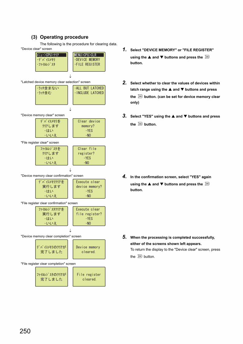
(3) Operating procedureThe following is the procedure for clearing data.
"Device clear" screen 1. Select "DEVICE MEMORY" or "FILE REGISTER"
using the and buttons and press the
button.
"Latched device memory clear selection" screen 2. Select whether to clear the values of devices within
latch range using the and buttons and press
the button. (can be set for device memory clear
only)
"Device memory clear" screen
"File register clear" screen
3. Select "YES" using the and buttons and press
the button.
"Device memory clear confirmation" screen
"File register clear confirmation" screen
4. In the confirmation screen, select "YES" again
using the and buttons and press the
button.
"Device memory clear completion" screen
"File register clear completion" screen
5. When the processing is completed successfully,
either of the screens shown left appears.
To return the display to the "Device clear" screen, press
the button.
OK
OK
OK
OK
OK
250
CHAPTER 4 DISPLAY UNIT FUNCTIONS
4
4.2
CP
U M
on
itor/T
est
4.2
.3 F
orce
d o
n/o
ff
4.2.3 Forced on/off
X and Y devices can be forcibly turned on or off with the display unit.
The forced on/off includes the following functions.
• Forced on/off registration
• Forced on/off clear
• Forced on/off batch clear
• Forced on/off list
(1) Screen transitionThe following shows screen transition of forced on/off.
OK
"Function selection" screen
"CPU monitor/test" screen
"Forced On/off" screen
"Forced on/off batch clear" screen "Forced on/off registration" screen
"Forced on/off list" screen"Forced on/off clear" screen
Forced on/off
251

(2) Forced on/off registrationSpecify a device (X or Y) and whether to turn on or off the specified device. The specified device and device
status are registered in a list. Devices that have already been registered can be reset. Up to 32 devices can be
registered.
Perform the following operation from the "forced on/off registration" screen.
When at least one device is registered, the MODE LED on the CPU module will be flashing in green.
"Forced on/off registration" screen 1. Switch a device using the and buttons.
"Forced on/off registration" screen 2. Move the cursor using the and buttons and
increase or decrease a device number using the
and buttons.
"Forced on/off registration" screen 3. Move the cursor using the and buttons and
switch on/off setting using the and buttons.
4. Pressing the button will register the setting and
will return the display to the "forced on/off" screen.
OK
252

CHAPTER 4 DISPLAY UNIT FUNCTIONS
4
4.2
CP
U M
on
itor/T
est
4.2
.3 F
orce
d o
n/o
ff
(3) Forced on/off clearRegistered devices are cleared one by one. Perform the following operation from the "forced on/off clear" screen.
(4) Forced on/off batch clearRegistered devices are batch-cleared. Perform the following operation from the "forced on/off batch clear"
screen.
(5) Forced on/off listRegistered devices are listed in the "forced on/off list" screen.
"Forced on/off clear" screen 1. Select a device to be cleared using the and
buttons.
2. Pressing the button will clear the selected
device.
"Forced on/off batch clear" screen 1. Select "YES" using the and buttons and press
the button.
"Forced on/off batch clear completion" screen 2. When the processing is completed successfully,
either of the screens shown left appears.
To return the display to the "Device clear" screen, press
the button.
OK
OK
OK
The screen is scrolled by one line by pressing
the or button once.
253

4.2.4 Scan time monitor
The current value, maximum value, and minimum value of scan time can be checked with the display unit. Values
stored in the special register of the CPU module are displayed.
*1 These values of an initial execution type program are not displayed.
(1) Screen transitionThe following shows screen transition of scan time monitor.
(2) Monitor dataThe current value, maximum value, and minimum value of scan time are displayed.
Displayed item Special register Description
Current value SD520, SD521 Current scan time
Maximum value SD526, SD527 Maximum scan time*1
Minimum value SD524, SD525 Minimum scan time*1
OK
"Function selection" screen
"CPU monitor/test" screen
"Scan time monitor" screen
Displayed up to third decimal place.
254

CHAPTER 4 DISPLAY UNIT FUNCTIONS
4
4.2
CP
U M
on
itor/T
est
4.2
.5 B
uilt-in
I/O fu
nctio
n m
on
itor
4.2.5 Built-in I/O function monitor
I/O status and setting values of the built-in I/O function can be checked with the display unit. Also, errors detected
during execution of the built-in I/O function can be cleared.
The built-in I/O monitor includes the following functions.
• Built-in positioning function monitor
• Built-in high-speed counter function monitor
• Built-in I/O function error clear
(1) Screen transitionThe following shows screen transition of built-in I/O function monitor.
OK
"Function selection" screen
"CPU monitor/test" screen
"Built-in I/O function monitor/error clear" screen
Built-in I/O function monitor
"Positioning function - monitor axis selection" screen
"High-speed counter function - monitor target selection" screen"Built-in I/O function error clear - axis/CH selection" screen
"High-speed counter function - monitor CH selection" screen
255

(2) Built-in positioning function monitorThe setting values of the built-in positioning function can be monitored.
(a) Displayed items
The following items are displayed.
(b) Operating procedure
The following is the procedure for monitoring the values.
(3) Built-in high-speed counter function monitorThe setting values of the built-in high-speed counter function can be monitored.
(a) Displayed items
The following items are displayed.
*1 This applies when "1-Phase Multiple of 1", "1-Phase Multiple of 1 (A Phase only)", or "CW/CCW" is set for "Pulse Input Mode".
*2 This applies when "200kpps" is set for "Counting Speed Setting".*3 If pulses exceeding the number of pulses shown in the performance specifications are input, this range may be
exceeded.
Displayed item Description Setting range
Position (p) Positioning range -2147483648 to 2147483647 pls
Velocity (v) Speed command (speed limit value) 0 to 200000 pps
Data No. Data No. of positioning being executed "ABSENT" or 1 to 10
Error code Error code of the built-in positioning function "ABSENT" or an error code is displayed.
"Positioning function - monitor axis selection" screen 1. Select "AXIS #1" or "AXIS #2" using the and
buttons and press the button.
"Positioning function monitor" screen 2. The displayed items are shown.
Displayed item Description Setting range
Current value (m) Current counter value -2147483648 to 2147483647
Frequency (f) A frequency of the high-speed counter function -100000 to 100000Hz *1
MeasurementMeasurement status of the high-speed counter
functionOperating/not operating
Rotation speed (r) Rotation speed of the high-speed counter function -12000000 to 12000000r/min*2*3
Error code Error code of the high-speed counter function "ABSENT" or an error code is displayed.
OK
256

CHAPTER 4 DISPLAY UNIT FUNCTIONS
4
4.2
CP
U M
on
itor/T
est
4.2
.5 B
uilt-in
I/O fu
nctio
n m
on
itor
(b) Operating procedure
The following is the procedure for monitoring the values."High-speed counter function - monitor CH selection" screen 1. Select "CH1" or "CH2" using the and buttons
and press the button.
"High-speed counter function - monitor target selection" screen 2. Select "PRESENT VAL MON", "PULSE
FREQUENCY", or "ROTATION SPD" using the
and buttons and press the button.
"High-speed counter function - current value monitor" screen
"High-speed counter function - frequency monitor" screen
"High-speed counter function - rotation speed monitor" screen
3. The displayed items are shown.
OK
OK
257

(4) Built-in I/O function error clearAn error can be cleared by specifying an axis of the positioning function or CH (channel) of the high-speed
counter function."Built-in I/O function error clear - axis/CH selection" screen 1. Select the target item using the and buttons
and press the button.
"Built-in I/O function - error clear confirmation" screen 2. Select "YES" using the and buttons and press
the button.
"Built-in I/O function - error clear completion" screen 3. When the error is cleared successfully, either of the
screens shown left appears.
To return to the "Built-in monitor/error clear" screen,
press the button.
OK
OK
OK
258

CHAPTER 4 DISPLAY UNIT FUNCTIONS
4
4.2
CP
U M
on
itor/T
est
4.2
.6 E
rror d
ispla
y/clea
r
4.2.6 Error display/clear
The current and past errors and their information can be checked with the display unit. Also, the current error can be
cleared.
The error display/clear includes the following functions.
• Current error monitor
• Error log display
• Error clear
(1) Screen transitionThe following shows screen transition of error display/clear.
OK
OK
OK
"Function selection" screen
"Error common information" screen
"Error individual information" screen" "Error information" screen
"Error display/clear" screen
Selecting "MONITOR"
Selecting
"CLEAR"
Selecting "LOG"
"Error log" screen
"Error clear" screen
"Error list" screen
"CPU monitor/test" screen
259

(2) Current error monitorThe information of latest and current CPU module error (including an annunciator) can be checked.
The current error monitor includes the following screens.
• "Error information" screen
• "Error common information" screen
• "Error individual information" screen
(a) Error information
If an error occurs, the following information is displayed.
(b) Error common information
If an error occurs, the following information is displayed.
The following items are displayed in the "error common information" screen.
Error common information DescriptionError common
informationDescription
Module No.Slot No./block No.
Program error location
File name
I/O No. SFC block specification
File name/drive nameDrive SFC step specification
File name SFC transition specification
Time (setting value) Time Step No./transition condition
Not error Sequence step No.
Current page/number of pagesError code
Time when an error occurred
Error message
Year and date when an error occurred
Current page/number of pages
Error common information
260

CHAPTER 4 DISPLAY UNIT FUNCTIONS
4
4.2
CP
U M
on
itor/T
est
4.2
.6 E
rror d
ispla
y/clea
r
(c) Error individual information
If an error occurs, the following information is displayed.
The following items are displayed in the "error individual information" screen.
(3) Error log displayErrors that have occurred in the CPU module are displayed in a list. The following table shows displayed items.
*1 Time when errors have occurred is listed in reverse chronological order.
(a) Operating procedure
The following is the procedure for displaying the errors.
Error individual
informationDescription
Error individual
informationDescription
File name/drive nameDrive Parameter No. Parameter No.
File name Annunciator No. F No.
Time (measured value) Time
File diagnostic information
Drive No.
Program error location
File name File name
SFC block specification Failure information 1
SFC step specification Failure information 2
SFC transition specification Failure information 3
Step No./transition conditionNot error
Sequence step No.
Displayed item Description
Display number Display order of error information (error code, error message)*1
Error code Error code of the corresponding error
Error message Error message of the corresponding error
"Error log" screen 1. Press the button.
"Error list" screen 2. To display error information, select the target error
log using the and buttons and press the
button.
Current page/number of pages
Error individual information
OK
OK
261

(4) Error clearContinuation errors can be cleared with the display unit.
Remove the error cause before clearing an error.For how to remove error causes, refer to the following.MELSEC-L CPU Module User's Manual (Hardware Design, Maintenance and Inspection)
(a) Operating procedure
The following is the procedure for clearing the error."Error clear" screen 1. Select an error to be cleared using the and
buttons and press the button.
"Error clear confirmation" screen 2. Select "YES" using the and buttons and press
the button.
"Error clear completion" screen 3. When the error is cleared successfully, either of the
screens shown left appears.
To return to the "Error clear" screen, press the
button.
OK
OK
OK
262

CHAPTER 4 DISPLAY UNIT FUNCTIONS
4
4.3
CP
U S
ettin
gs
4.3
.1 C
lock se
tting
4.3 CPU Settings
The internal time of the CPU module can be checked and changed with the display unit.
4.3.1 Clock setting
The internal time of the CPU module can be set.
(1) Screen transitionThe following shows screen transition of clock setting.
(2) Setting itemThe following table shows items that can be set by clock setting.
Item Setting range Item Setting range
Year 1980 to 2079 Hour 00 to 23
Month 1 to 12 Minute 00 to 59
Day 1 to 31 Second 00 to 59
OK
"Function selection" screen
"CPU settings" screen
"Clock setting" screen
263

(3) Operating procedureThe following is the procedure for setting the clock data.
"Clock setting" screen 1. Move the cursor using the and buttons,
increase or decrease a time value using the and
buttons, and press the button.
"Clock setting confirmation" screen 2. Select "YES" using the and buttons and press
the button.
"Clock setting completion" screen 3. When the setting is completed, either of the screens
shown left appears.
To return to the "CPU settings" screen, press the
button.
OK
OK
OK
264

CHAPTER 4 DISPLAY UNIT FUNCTIONS
4
4.4
Mo
du
le M
on
itor/T
est
4.4
.1 B
uffe
r me
mo
ry mo
nito
r/test
4.4 Module Monitor/Test
The buffer memory values of intelligent function modules (including the LCPU with the built-in CC-Link function) can be
checked and changed with the display unit.* 1
*1 The values of MELSEC-AnS/QnAS series modules mounted on the LA1S extension base unit cannot be checked.
4.4.1 Buffer memory monitor/test
Buffer memory values can be monitored and tested.
(1) Screen transitionThe following shows screen transition of buffer memory monitor/test.
OK
OKOK
OK
OK
OK
OK
OK
OK
OK
OK
OK
,
"Function selection" screen
"Module monitor/test" screen
"Buffer memory address setting" screen
"Module monitor/test_module specification" screen
"Module monitor/test_module list selection" screen
"Input format of buffer memory address selection" screen
"Buffer memory monitor" screen
"Display format selection" screen"Device comment display selection" screen
Buffer memory test
"Buffer memory test value check" screen
"Buffer memory test" screen
Buffer memory monitor
"Module monitor/test_start I/O No. specification" screen
265

(2) Specifying a moduleA module to be monitored or tested is specified by the following ways.
• Start I/O No. specification
• Module selection
(a) Start I/O No. specification
Perform the following operation.
(b) Module selection
Perform the following operation.
"Module monitor/test_start I/O No. specification" screen 1. Move the cursor using the and buttons,
increase or decrease a start I/O No. using the and
buttons, and press the button.
"Module monitor/test_module selection" screen 1. Select a target item using the and buttons and
press the button.
OK
OK
266

CHAPTER 4 DISPLAY UNIT FUNCTIONS
4
4.4
Mo
du
le M
on
itor/T
est
4.4
.1 B
uffe
r me
mo
ry mo
nito
r/test
(3) Specifying a buffer memory addressSpecify the buffer memory address of the module selected in (2) in this section. Perform the following operation.
(4) Specifying display formatPerform the following operation.
"Module monitor/test" screen 1. Press the button.
"Buffer memory address input format selection" screen 2. Select the input format of a buffer memory address
using the and buttons and press the
button.
"Buffer memory address specification" screen 3. Move the cursor using the and buttons,
increase or decrease an address digit using the
and buttons, and press the button.
"Buffer memory monitor" screen 1. Press the button.
"Display format selection" screen 2. Select display format using the and buttons
and press the button.
OK
OK
OK
OK
267

(5) Specifying a device comment
To display a device with device comment, perform the following operation.* 1*2
*1 Device comments are displayed only in the following screens. "Buffer memory monitor" screen "Buffer memory test value check" screen "Buffer memory test" screen
*2 To display a device comment, preset "Comment File Used in a Command" in the PLC File tab of the PLC Parameter dialog box.
(6) Buffer memory monitorThe start I/O No., buffer memory address, display format, buffer memory value, and bit status of the buffer
memory value of the specified module can be monitored.
The description of displayed items is the same as that of the device monitor. ( Page 245, Section 4.2.1 (5))
"Buffer memory monitor" screen 1. Press the button.
"Device comment display selection" screen 2. Select "DSP DEV COMMENT" using the and
buttons and press the button.OK
A buffer memory address to be monitored can be changed
by 1 word with the and buttons.
Start I/O number of a module to be monitored
Display format
Buffer memory valueBit position counted from the
specified buffer memory address
On/off status of bits
ON :
OFF:
268
CHAPTER 4 DISPLAY UNIT FUNCTIONS
4
4.4
Mo
du
le M
on
itor/T
est
4.4
.1 B
uffe
r me
mo
ry mo
nito
r/test
(7) Buffer memory testA buffer memory value can be changed.
Since the value displayed in the "buffer memory test value check" screen is used for testing, if the relevant buffer memory is being used in a program, the displayed value may differ from the one set in the "buffer memory test" screen.
"Buffer memory monitor" screen 1. Press the button.
"Buffer memory test value check" screen 2. Select the target address using the and
buttons and press the button. The cursor
moves to the buffer memory value. Increase or
decrease the value using the and buttons.
3. Pressing the button will update the value set in
buffer memory test.
OK
OK
OK
269

4.5 Module Settings
Values set to intelligent function modules can be checked and changed with the display unit.
4.5.1 Initial setting change
The initial setting value of an intelligent function module can be changed.
The changed value is reflected to the CPU module after any of the following operations are performed.
• Powering off and then on the CPU module
• Resetting the CPU module
• Setting the CPU module from STOP to RUN*1
*1 Perform this operation twice. (STOPRUNSTOPRUN)
Write the following items to the CPU module before changing the initial setting. If the setting is changed before the items are written, an error message will be displayed.
• Intelligent function module parameters ( Page 77, Section 2.11 (1))• Menu definition file ( Page 272, Section 4.5.1 (2))
270
CHAPTER 4 DISPLAY UNIT FUNCTIONS
4
4.5
Mo
du
le S
ettin
gs
4.5
.1 In
itial se
tting
cha
ng
e
(1) Screen transitionThe following shows screen transition of initial setting change.
Levels lower than the "initial setting change" screen depend on intelligent function module used.
Manual for the intelligent function module used
OK OK
OK OK
"Function selection" screen
"Initial setting change" screen
"Module settiong_module specification" screen
"Module setting_module selection" screen
"Module setting_start I/O
No. specification" screen
271

(2) Registering/canceling display unit menuTo change an initial setting value with the display unit, write a menu definition file to the CPU module. Select the
standard ROM or an SD memory card as a storage location.* 1*2*3
[Online] [Register/Cancel Display Module Menu...]
*1 GX Developer cannot write menu definition files.*2 When a menu definition file has been stored in an SD memory card, the file in the SD memory card will be written even
if a menu definition file is created and stored in the standard ROM.*3 For the versions of GX Works2 that supports intelligent function modules, refer to the following.
GX Works2 Version 1 Operating Manual (Common)
272

CHAPTER 4 DISPLAY UNIT FUNCTIONS
4
4.6
Use
r Me
ssag
e
4.6 User Message
Executing User message instruction (UMSG) displays a user message on the display unit. User messages are user-
defined messages for display unit.
For details on User message instruction, refer to the following.
MELSEC-Q/L Programming Manual (Common Instruction)
● Under the "USER MESSAGE" menu selected from the "function selection" screen, the user message displayed last can be displayed again.
However, the user message will not be displayed if it is not held in the following cases.• A user message is attempted to be displayed after User message instruction where empty character strings have
been specified as an argument is executed.• A user message is attempted to be displayed while User message instruction has not been executed after the
CPU module is powered off and then on or is reset.• User message instruction where a null code (00H) has been specified as an argument is executed while a user
message is displayed.
*1 When a displayed language is switched by language setting, the language of a user message is not changed.
● A user message is displayed whenever the User message instruction is on the rising edge or there is a change in the message. If the intervals between the rising edges or changes in user message are too short, a user message will pop up
continually and therefore, operation of the display unit will be frequently interrupted. In this case, holding down the button on the display unit for a while will disable the pop-up display. For how to enable pop-up display, refer to Page 286, Section 4.8.4.
When the module receives a message during function
execution, the message is displayed on the display unit.
Executing user message instruction (UMSG)
will issue a user message.
OK
"Function selection" screen "User message menu" screen "User message" screen *1
ESC
273

4.7 Memory Card Operation
File operations between the CPU module and an SD memory card can be performed with the display unit.
The memory card operation includes the following functions.
• File list/delete ("FILE LIST/DEL")
• Free space check ("FREE SPACE")
• Batch save ("BATCH SAVING")
• Batch load ("BATCH LOADING")
To perform the memory card operation, an SD memory card must be inserted to the CPU module, and use of the card must be enabled.If any one of the memory card operation is executed under the following conditions, an error message is displayed.
• An SD memory card is not inserted.• Use of an SD memory card is disabled by SM606 (SD memory card forced disable instruction).
4.7.1 File list/delete
Folders and files stored in an SD memory card can be displayed in a list.
The time stamp and size information of a specified folder or file can be checked. Also, a specified folder or file can be
deleted.
(1) Screen transitionThe following shows screen transition of the file list/delete function.
"Function selection" screen
"File list" screen
"Folder/file delete" screen"Time stamp/size display" screen
"File list" screen for the selected folder
"Memory card operation menu" screen
"Folder/file operation menu" screen
File list/delete
274
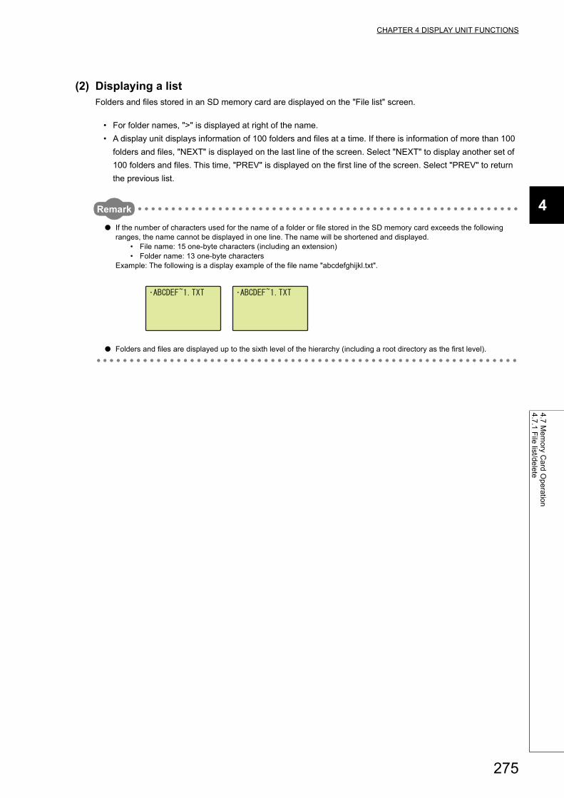
CHAPTER 4 DISPLAY UNIT FUNCTIONS
4
4.7
Me
mo
ry Ca
rd O
pe
ratio
n4
.7.1
File
list/de
lete
(2) Displaying a listFolders and files stored in an SD memory card are displayed on the "File list" screen.
• For folder names, ">" is displayed at right of the name.
• A display unit displays information of 100 folders and files at a time. If there is information of more than 100
folders and files, "NEXT" is displayed on the last line of the screen. Select "NEXT" to display another set of
100 folders and files. This time, "PREV" is displayed on the first line of the screen. Select "PREV" to return
the previous list.
Remark
● If the number of characters used for the name of a folder or file stored in the SD memory card exceeds the following ranges, the name cannot be displayed in one line. The name will be shortened and displayed.
• File name: 15 one-byte characters (including an extension)• Folder name: 13 one-byte characters
Example: The following is a display example of the file name "abcdefghijkl.txt".
● Folders and files are displayed up to the sixth level of the hierarchy (including a root directory as the first level).
275

(3) Displaying the time stamp and sizeThe time stamp and size of folders and files stored in an SD memory card are displayed.
(a) Operating procedure
The following is the procedure for displaying the time stamp and size information."File list" screen 1. Select a folder or file using the and buttons in
the "File list" screen, and press the button.
"Folder/file operation menu" screen 2. Select "TIME STAMP/SIZE" using the and
buttons and press the button.
Time stamp/size" screen 3. The time stamp and size of the specified folder or
file are displayed.
To return to the "Folder/file operation menu" screen,
1press the button.
Folder/file name
Time stamp
Size
OK
OK
OK
276

CHAPTER 4 DISPLAY UNIT FUNCTIONS
4
4.7
Me
mo
ry Ca
rd O
pe
ratio
n4
.7.1
File
list/de
lete
(4) Deleting a folder or fileFolders and files stored in an SD memory card are deleted.
(a) Operating procedure
The following is the procedure for deleting a folder or file.
When a folder is specified, all folders and files in the specified folder are deleted.However, if the folder contains any read-only file, the read-only file will not be deleted and the folder remains. (Folders and files other than the read-only file will be deleted.)To delete the folder that contains any read-only file, delete the read-only file first, and then delete the folder.
"File list" screen 1. Select a folder or file using the and buttons in
the "File list" screen, and press the button.
"Folder/file operation menu" screen 2. Select "DELETE" using the and buttons and
press the button.
"Folder/file delete" screen 3. Select "YES" using the and buttons and press
the button.
"Folder/file delete completion" screen 4. The specified folder or file is deleted.
To return to the "File list" screen, press the button.
OK
OK
OK
OK
277

(b) Precautions
The following online functions cannot be executed while a folder or file is being deleted. If executed, an error
response is returned to the request source
Category Function
Drive operation
Format PLC memory
Clear PLC memory (Clear all file registers)
Write title
Arrange PLC memory
File operation
Write to PLC
Delete PLC data
Write PLC user data
Delete PLC user data
Password registration
Trace Sampling trace registration
Data logging Data logging registration
FTP function All operations and commands
OthersCPU module change function with SD memory card
Register/cancel display unit menu
278

CHAPTER 4 DISPLAY UNIT FUNCTIONS
4
4.7
Me
mo
ry Ca
rd O
pe
ratio
n4
.7.2
Fre
e sp
ace
disp
lay
4.7.2 Free space display
The free space on the SD memory card that is inserted to the CPU module can be displayed with the display unit.
(1) Operating procedureThe following is the procedure for displaying the free memory space.
"Memory card operation menu" screen 1. Select "FREE SPACE" using the and buttons
and press the button.
"Free space display menu" screen 2. Press the button.
"Free space display" screen 3. Free space of the SD memory card is displayed.
Press the button to return to the "Memory card
operation menu" screen.
OK
OK
OK
279

4.7.3 Batch save
Data (such as program file and parameter file) in the CPU module can be saved into an SD memory card.
(1) Operating procedureThe following is the procedure for batch-saving data.
*1 The following items are displayed on the "Batch saving" screen.
"Memory card operation menu" screen 1. Select "BATCH SAVING" using the and buttons
and press the button.
"Batch save execution" screen 2. Select "YES" using the and buttons and press
the button.
"Batch saving" screen 3. The batch data processing starts.* 1
During the batch data processing, button operations on
the display unit are disabled.
"Batch save completion" screen 4. When the processing is completed successfully,
either of the screens shown left appears.
To return to the "Memory card operation menu" screen,
press the button.
A "SaveLoad" folder is created in the SD memory card.
OK
OK
OK
Progress rate (Overall)File name
Progress rate (Individual file)
280

CHAPTER 4 DISPLAY UNIT FUNCTIONS
4
4.7
Me
mo
ry Ca
rd O
pe
ratio
n4
.7.4
Ba
tch lo
ad
4.7.4 Batch load
Data saved in the SD memory card by the batch save function can be read to the CPU module.
This function can be executed only when the CPU module is in STOP status.
(1) Operating procedureThe following is the procedure for batch-loading data.
"Memory card operation menu" screen 1. Select "BATCH LOADING" using the and
buttons and press the button.
"Batch load target folder" screen 2. Select a load-target folder using the and
buttons and press the button.
Folders in the "SaveLoad" folder can only be loaded.
"Batch load execution" screen 3. Select "YES" using the and buttons and press
the button.
To overwrite read-only files, the overwrite confirmation
screen appears.
"Drive format execution" screen 4. Select "YES" using the and buttons to format
all drives in the CPU module and press the
button. *1
When "NO" is selected, the batch load function is
executed without formatting the drives.
"Drive formatting" screen
"Batch loading" screen
5. When all drives are formatted, the "Drive
formatting" screen is displayed and then the "Batch
loading" screen is displayed.* 2
During the format processing or the batch load
processing, button operations on the display unit are
disabled.
OK
OK
OK
OK
281

*1 The program memory, standard RAM, and standard ROM are formatted. The SD memory card is not formatted.*2 The following items are displayed on the "Batch loading" screen.
● The batch load processing cannot be performed if the SD memory card is write-protected.Remove write protection from the SD memory card, and execute the function.
● If a folder or file (including read-only files) with the same name exists in the load-destination CPU module, data in the corresponding folder or file will be overwritten.
● When the batch load function is executed without formatting the drives, data in the folders that are not targeted for batch load in the load-destination CPU module will remain the same.
"Batch load completion" screen 6. When the processing is completed successfully,
either of the screens shown left appears.
To return to the "Memory card operation menu" screen,
press the button.OK
Progress rate (Overall)File name
Progress rate (Individual file)
282

CHAPTER 4 DISPLAY UNIT FUNCTIONS
4
4.8
Op
tion
s4
.8.1
La
ng
ua
ge
settin
g
4.8 Options
The display format and basic settings of the display unit can be configured under the "OPTIONS" menu selected from
the "function selection" screen. The option settings can be backed up to the CPU module without a battery.* 1*2
*1 The pop-up setting is not backed up.*2 When the display unit is removed and attached to another CPU module, the display unit operates according to settings
stored in the CPU module to which the display unit is currently attached.
The option settings include the following settings.
• Language setting
• Contrast adjustment
• Lighting period setting
• Pop-up display
4.8.1 Language setting
A displayed language can be changed.
(1) Operating procedureThe following is the procedure for setting the language.
Information of language displayed on the display unit can be checked in SD581 (Displayed language information).MELSEC-L CPU Module User's Manual (Hardware Design, Maintenance and Inspection)
"Options" screen 1. Select "LANGUAGE" using the and buttons
and press the button.
"Language setting" screen 2. Switch the language using the and buttons and
press the button.
OK
OK
283

4.8.2 Contrast adjustment
Tone of displayed characters can be set.
(1) Setting rangeTone can be selected from 0 (light) to 9 (dark). (default: 3)
(2) Operating procedurePerform the following operation.
"Options" screen 1. Select "CONTRAST" using the and buttons
and press the button.
"Contrast adjustment" screen 2. Set a contrast value using the and buttons and
press the button.
OK
OK
284

CHAPTER 4 DISPLAY UNIT FUNCTIONS
4
4.8
Op
tion
s4
.8.3
Lig
htin
g p
erio
d se
tting
4.8.3 Lighting period setting
The lighting period of the backlight on the display unit can be set.
(1) Setting rangeThe following shows periods that can be set. (default: 5MIN)
(2) Operating procedurePerform the following operation.
• 1MIN • 3MIN • 5MIN • 10MIN • 15MIN • 30MIN • 60MIN • LIGHT ALWAYS ON
"Options" screen 1. Select "BACKLIGHT" using the and buttons
and press the button.
"Lighting period setting" screen 2. Set a lighting period using the and buttons and
press the button.
OK
OK
285

4.8.4 Pop-up display
A pop-up screen showing a user message ( Page 273, Section 4.6) can be enabled.
(1) Operating procedureEnable pop-up display by the following operation.
"Options" screen 1. Select "POPUP" using the and buttons and
press the button.
"Pop-up" screen 2. Press the button.
"Pop-up setting confirmation" screen 3. Select "YES" using the and buttons and press
the button.
"Pop-up setting completion" screen 4. When the setting is completed, either of the screens
shown left appears.
Press the button to return to the "Pop-up" screen.
OK
OK
OK
286

PART 3 DEVICES, CONSTANTS
In this part, the devices and constants used in the CPU module are described.
CHAPTER 5 DEVICES . . . . . . . . . . . . . . . . . . . . . . . . . . . . . . . . . . . . . . . . . . . . . . . . . . 288
CHAPTER 6 CONSTANTS . . . . . . . . . . . . . . . . . . . . . . . . . . . . . . . . . . . . . . . . . . . . . . . 342
CHAPTER 7 CONVENIENT USAGE OF DEVICES . . . . . . . . . . . . . . . . . . . . . . . . . . . . 344
287

CHAPTER 5 DEVICES
This chapter describes the devices that can be used in the CPU module.
5.1 Device List
The following table shows the devices used in the CPU module and applicable ranges.
Classification Type Device nameDefault Parameter-
set rangeReference
Points Range
Internal user
device
Bit device
Input 8192 X0 to X1FFF Hexadecimal
Cannot be set
Page 293,
Section 5.2.1
Output 8192 Y0 to Y1FFF HexadecimalPage 293,
Section 5.2.2
Internal relay 8192 M0 to M8191 Decimal
Can be set (up
to 29K words for
internal user
devices in
total)*8*9
Page 294,
Section 5.2.3
Latch relay 8192 L0 to L8191 DecimalPage 294,
Section 5.2.4
Link relay 8192 B0 to B1FFF HexadecimalPage 294,
Section 5.2.5
Annunciator 2048 F0 to F2047 DecimalPage 295,
Section 5.2.6
Link special relay 2048 SB0 to SB7FF HexadecimalPage 298,
Section 5.2.7
Edge relay 2048 V0 to V2047 DecimalPage 298,
Section 5.2.8
Step relay 8192 S0 to S8191 DecimalPage 299,
Section 5.2.9
• Bit device
(contacts and
coils)
• Word device
(current value)
Timer 2048 T0 to T2047 Decimal Page 299,
Section 5.2.10Retentive timer 0 (ST0 to ST2047) Decimal
Counter 1024 C0 to C1023 DecimalPage 308,
Section 5.2.11
Word device
Data register 12288 D0 to D12287 DecimalPage 311,
Section 5.2.12
Link register 8192 W0 to W1FFF HexadecimalPage 312,
Section 5.2.13
Link register 2048 SW0 to SW7FF HexadecimalPage 313,
Section 5.2.14
Internal system
device
Bit device
Function input 16 FX0 to FXF Hexadecimal
Cannot be set
Page 314,
Section 5.3.1Function output 16 FY0 to FYF Hexadecimal
Special relay 2048 SM0 to SM2047 DecimalPage 316,
Section 5.3.2
Word device
Function register 5 FD0 to FD4 DecimalPage 314,
Section 5.3.1
Special register 2048 SD0 to SD2047 DecimalPage 316,
Section 5.3.3
288

CHAPTER 5 DEVICES
5
5.1
De
vice L
ist
*1 The number of points for the L02SCPU, L02SCPU-P, L02CPU, and L02CPU-P are 32K points (D12288 to D45055).*2 The number of points that can be actually used varies depending on the intelligent function module.
Manual for the intelligent function module used*3 The range for the L02SCPU, L02SCPU-P, L02CPU, and L02CPU-P is 0 to 64K in total.*4 The number of points for the L02SCPU, L02SCPU-P, L02CPU, and L02CPU-P is 128 points (BL0 to BL127).*5 The range for the L02SCPU, L02SCPU-P, L02CPU, and L02CPU-P is U0 to U3F.*6 This device can be used in the CPU module whose serial number (first five digits) is "13012" or later.*7 For CC-Link IE Field Network, J\W0 to J\W1FFF are for RWw (8192 points), and J\W2000 to J\W3FFF are for
RWr (8192 points).*8 When changing the number of device points, refer to the precautions on Page 293, Section 5.2 (1).*9 The device point of the step relay for the CPU module whose serial number (first five digits) is "15101" or earlier is either
0K or 8K.*10 For the L06CPU, L06CPU-P, L26CPU, L26CPU-P, L26CPU-BT, L26CPU-PBT with a serial number (first five digits) of
"16042" or later, the pointer for auto assignment device can be used up to 32768 points by using the GX Works2. (The PC parameters should be set. ( Page 362, Appendix 1.2 (8)))
Link direct
device*6
Bit device
Link input 16384 Jn\X0 to Jn\X3FFF Hexadecimal
Cannot be setPage 317,
Section 5.4
Link output 16384 Jn\Y0 to Jn\Y3FFF Hexadecimal
Link special relay 512 Jn\SB0 to Jn\SB1FF Hexadecimal
Word device
Link register 16384Jn\W0 to
Jn\W3FFF*7Hexadecimal
Link special register 512Jn\SW0 to
Jn\SW1FFHexadecimal
Module access
deviceWord device
Intelligent function
module device65536
Un\G0 to
Un\G65535*2Decimal Cannot be set
Page 320,
Section 5.5
Index register or
standard device
register
Word device
Index register or
standard device
register
20 Z0 to Z19 Decimal Cannot be setPage 322,
Section 5.6
File register Word device File register 0 Decimal0 to 384K points
in total*3 (in
increments of
1K)
Page 326,
Section 5.7
Extended data
registerWord device
Extended data
register128K*1
D12288 to
D143359*1Decimal
Page 330,
Section 5.8Extended link
registerWord device Extended link register 0 Hexadecimal
Nesting Nesting 15 N0 to N14 Decimal Cannot be setPage 335,
Section 5.9
Pointer
Pointer 4096*10 P0 to P4095*10 Decimal
Cannot be set
Page 336,
Section 5.10
Interrupt pointer 256 I0 to I255 DecimalPage 339,
Section 5.11
Others
Bit device SFC block device 320*4 BL0 to BL319*4 Decimal
Cannot be set
Page 340,
Section 5.12.1
I/O No. specification
device U0 to UFF*5 Hexadecimal
Page 340,
Section 5.12.2
Macro instruction
argument device10 VD0 to VD9 Decimal
Page 341,
Section 5.12.3
Classification Type Device nameDefault Parameter-
set rangeReference
Points Range
289

5.2 Internal User Devices
Internal user devices can be used for various user applications.
(1) Points for internal user devicesSet the number of device points to be used.
Project window [Parameter] [PLC Parameter] [Device]
When changing device points, note the following.
• The points for the input (X), output (Y) cannot be changed.
• Set each device in increments of 16 points.
• Up to 29K words can be set for total internal user devices.
• The maximum number of points for a bit device is 32K. For an internal relay and link relay, the maximum
number of points can be set up to 60K.
• One point of the timer, retentive timer, and counter is regarded as one word device point and two bit device
points. ( Page 291, Section 5.2 (2))
290

CHAPTER 5 DEVICES
5
5.2
Inte
rna
l Use
r De
vices
● When changing device points, the following refresh ranges must not exceed the corresponding device ranges.• Link refresh with CC-Link IE Field Network master/local module• Link refresh with CC-Link IE Field Network Basic• Auto refresh with CC-Link• Auto refresh with intelligent function module
If device points are set exceeding the corresponding device range, data may be written to any other device or an error may occur.
● If the device points of the internal user devices are changed and the parameters are written from the "Write to PLC" screen, the device address may be shifted and does not correspond to the original stored value. Because the shifted value might be used for the operation, the following files, which are created by using the parameters before the device point change, cannot be used under existing condition.
• Sequence program files• SFC program files• ST program files
When change the device points of the internal user devices, perform the following operations from a programming tool.[Before changing the device points of the internal user devices]Read devices to be used and each program from the CPU module.[After the device points of the internal user devices are changed]Write the devices and each program, which were read before the device point change, to the CPU module.
For the read/write of devices and programs, refer to the following.Operating manual for the programming tool used
(2) Memory sizeSet the internal user devices so that the following condition is satisfied.
(Bit device size) + (Timer, retentive timer, and counter sizes) + (Word device size) 29K words
• For bit devices, 16 points are calculated as one word.
• For the timer, retentive timer, and counter, 16 points are calculated as 18 words.
• For word devices, 16 points are calculated as 16 words.
16(Bit device size) =
(X + Y + M + L + B + F + SB + V + S)(Words)
16(Timer, retentive timer, or counter size) =
(T + ST + C) 18 (Words)
16(Word device size) =
(D + W + SW) 16 (Words)
291

(3) Device point assignment exampleThe following table shows device point assignment examples based on the device point assignment sheet in
Appendix.6.
*1 The points are fixed by the system (cannot be changed) for the LCPU whose serial number (first five digits) is "15101" or earlier. However, the points for the step relay (S) can be changed to 0.
*2 Up to 32K points can be set for each device (60K for the internal relay and link relay).*3 Enter the values multiplied or divided by the number shown in the Size (words) column.
Device name SymbolNumeric
notation
Number of device point*2 Restriction check
Points Range Size (words)*3 Points (bits)*2
Input relay*1 X 16 8K (8192) X0000 to X1FFF 16 512 1 8192
Output relay*1 Y 16 8K (8192) Y0000 to Y1FFF 16 512 1 8192
Internal relay M 10 16K (16384) M0 to M16383 16 1024 1 16384
Latch relay L 10 4K (4096) L0 to L4095 16 256 1 4096
Link relay B 16 4K (4096) B0000 to B0FFF 16 256 1 4096
Annunciator F 10 1K (1024) F0 to F1023 16 64 1 1024
Link special relay SB 16 2K (2048) SB0000 to SB07FF 16 128 1 2048
Edge relay V 10 1K (1024) V0 to V1023 16 64 1 1024
Step relay*1 S 10 8K (8192) S0 to S8191 16 512 1 8192
Timer T 10 2K (2048) T0 to T2047 2304 2 4096
Retentive timer ST 10 2K (2048) ST0 to ST2047 2304 2 4096
Counter C 10 1K (1024) C0 to C1023 1152 2 2048
Data register D 10 14K (14336) D0 to D14335 1 14336
Link register W 16 4K (4096) W0000 to W4095 1 4096
Link special register SW 16 2K (2048) SW0000 to SW07FF 1 2048
Total29568
(29696 or less)63488
18
16
18
16
18
16
292

CHAPTER 5 DEVICES
5
5.2
Inte
rna
l Use
r De
vices
5.2
.1 In
pu
t (X)
5.2.1 Input (X)
Inputs are the device used to obtain the on and off information from external devices to a CPU module.
(1) Concept of inputOne input point is assumed to be a virtual relay Xn in the CPU module. Programs use the normally open or
closed contact of Xn.
The input (X) can also be used for refresh target device (CPU module side) of remote input (RX) in CC-Link IE
Field Network, CC-Link IE Field Network Basic, or CC-Link.
5.2.2 Output (Y)
The output (Y) is used to output control results in programs to external devices.
1 2 3
Push-button switch
Selector switch
Digital switch
Input (X)
CPU module
PB2
PB1
X0
X1
XF
PB16
Input circuit (external device) Program
Programmable
controller
Virtual relay
CPU module
Output (Y)
Signal lamp
Digital display
Contactor
293

5.2.3 Internal relay (M)
The internal relay (M) is a device for auxiliary relays used in the CPU module. All of the internal relay are set to off
when:
• the CPU module is powered off and then on,
• the CPU module is reset, or
• the latch clear is executed. ( Page 88, Section 3.4)
The internal relay cannot be latched (data retention during power failure). Use the latch relay (L) when latch is required. ( Page 294, Section 5.2.4)
5.2.4 Latch relay (L)
The latch relay (L) is a device for auxiliary relays that can be latched inside the CPU module. During power failure,
on/off information are retained by the battery in the CPU module. The previous on/off information are retained even
after performing the following to the CPU module.
• Power OFFON
• Reset
The latch relay is turned off by the latch clear operation.
Scan time is prolonged when the latch relay is used. ( Page 353, Appendix 1.2)
5.2.5 Link relay (B)
The link relay is an internal relay whose point is input in hexadecimal. In the range where the network parameters are
not set, this relay can be used as an internal relay or a latch relay.
• The range where a link relay is not latched: Same as the range for an internal relay
• The range where a link relay is latched: Same as the range for a latch relay
When using a link device in the network module by using the points of the link register in the CPU module (default: 8192 points) or greater, change the points setting of the link register in the "Device" of the "PLC Parameter".
294

CHAPTER 5 DEVICES
5
5.2
Inte
rna
l Use
r De
vices
5.2
.6 A
nn
un
ciato
r (F)
5.2.6 Annunciator (F)
The annunciator (F) is an internal relay which can be effectively used in fault detection programs for user-created
system. Whenever an annunciator is turned on, SM62 turns on and the annunciator number is stored in SD62 to
SD79. By monitoring SD62 to SD79, the system can be checked for error and failure.
Ex. When F5 is turned on, the corresponding annunciator number is output to the outside.
(1) Turning on the annunciatorUse either of the following instructions.
(a) SET F instruction
Annunciator turns on only on the leading edge of an input condition. Even if the input condition turns off, the
annunciator is held on. Using many annunciator numbers can shorten scan time more than using the OUT F
instruction.
(b) OUT F instruction
Since the processing is performed for every scan, the scan time is longer than the case of using the SET F
instruction.
If the annunciator is turned on with any instruction other than SET F and OUT F (for example, the MOV instruction), the same operation as the internal relay (M) is performed. The ON information is not stored in SM62, and annunciator numbers are not stored in SD62 and SD64 to SD79.
SM62
SD62
SD63
SD64
SD65
SD79
0
0
[Fault detection program]
Outputs number of
the annunciator that turned on.
Annunciator ON detection
OFF ON
0 5
0 1
0 5
295

(2) Processing after annunciator onWhenever an annunciator is turned on, SM62 turns on and the following data are stored in SD62 to SD79. The
annunciator number in SD62 is registered to the memory for error history storage.
The USER LED on the front of the CPU module turns on (red).
Whether to turn on the USER LED can be set using the LED control function ( Page 169, Section 3.26).
(3) Turning off the annunciatorUse any of the following instructions.
(a) RST F instruction
This is used to turn off the annunciator number that was turned on with the SET F instruction.
(b) LEDR instruction
This is used to turn off the annunciator number stored in SD62 and SD64.
(c) BKRST instruction
This is used to turn off all of the annunciator numbers within the specified range.
(d) OUT F instruction
One annunciator number can be turned on or off with the same instruction. However, even if an annunciator
number is turned off with the OUT F instruction, the off processing described in (4) in this section is not
performed. If the annunciator is turned off with the OUT F instruction, execution of the RST F LEDR, or
BKRST instruction is required.
0
0
0
0
0
0
0
SD62
SD63
SD64
SD65
SD66
SD67
SD79
50
1
50
0
0
0
0
50
2
50
25
0
0
0
50
3
50
25
1023
0
0
SET F50 SET F25 SET F1023
1) Turned-on annunciator numbers are stored in
SD64 to SD79 in order.
3) SD63 value is
incremented by "1".
2) The annunciator number in
SD64 is stored in SD62.
Up to 16 annunciator numbers
can be stored
296

CHAPTER 5 DEVICES
5
5.2
Inte
rna
l Use
r De
vices
5.2
.6 A
nn
un
ciato
r (F)
(4) Processing after annunciator off• Data stored in the special register (SD62 to SD79) when the annunciator is turned off with the RST F or
BKRST instruction
• Data stored in the special register (SD62 to SD79) after execution of the LEDR instruction
If the LEDR instruction is executed while the annunciator is on and at the same time the operation continuation error that has higher priority than the annunciator has occurred, the LEDR instruction clears the higher priority error. To execute the LEDR instruction, remove the error whose priority is higher than that of the annunciator.
• LED indication
When all of the annunciator numbers in SD64 to SD79 turn off, the USER LED will turn off.
1) The specified annunciator number is deleted,
and the other annunciator numbers in the register
addressed after the deleted one are shifted
accordingly.
2) If the existing annunciator number in SD64 is
turned off, a new annunciator number stored in
SD64 will be stored in SD62.
3) SD63 value is decremented by "1". If the SD63
value is changed to "0", SM62 is turned off.
0
0
0
0
0
0
0
SD62
SD63
SD64
SD65
SD66
SD67
SD79
50
1
50
0
0
0
0
50
2
50
25
0
0
0
50
3
50
25
1023
0
0
SET F50 SET F25 SET F1023
50
2
50
1023
0
0
0
RST F25
1) The annunciator number in SD64 is deleted,
and the other annunciator numbers in
the register addressed SD65 and after are
shifted accordingly.
2) The annunciator number in SD64 is stored
in SD62.
3) SD63 value is decremented by "1".
If the SD63 value is changed to "0", SM62 is
turned off.
0
0
0
0
0
0
0
SD62
SD63
SD64
SD65
SD66
SD67
SD79
50
1
50
0
0
0
0
50
2
50
25
0
0
0
50
3
50
25
1023
0
0
SET F50 SET F25 SET F1023
25
2
25
1023
0
0
0
LEDR
297

5.2.7 Link special relay (SB)
The link special relay (SB) is a relay that indicates communication status and error detection status of the CC-Link IE
Field Network master/local module or the CC-Link system master/local module. The relay is turned on or off according
to various factors that occur during data link. Status of the data link can be confirmed by monitoring the link special
relay.
Manuals for each network module
5.2.8 Edge relay (V)
The edge relay (V) is a device in which the on/off information from the beginning of the ladder block. The EGP/EGF
instructions only can be used. The edge relay of the same number cannot be set.
Ex. Detecting a leading edge and execute it in the program configured using index modification
*1 The on/off information for X0Z1 is stored in the V0Z1 edge relay. For example, the on/off information of X0 is stored in V0, and that of X1 is stored in V1.
Stores on/off information of X0, X1, and X10.
Returns to FOR instruction.
*1 *1
Clears index register (Z1).
Specifies the number of repeats
(10 times).
Turns on M0Z1 for 1 scan, followed
by rise of X0Z1.
Increments (+1) index register (Z1).
[Program example]
[Timing chart]
When Z1 = 0
When Z1 = 1
X0
M0
V0
X1
M1
V1
OFF
OFF
OFF
OFF
OFF
OFF
ON
ON
ON
ON
ON
ON
1 scan
1 scan
Turns on for 1 scan by rise of X1.
Turns on for 1 scan by rise of X0.
298

CHAPTER 5 DEVICES
5
5.2
Inte
rna
l Use
r De
vices
5.2
.9 S
tep
rela
y (S)
5.2.9 Step relay (S)
This device is provided for SFC programs. ( MELSEC-Q/L/QnA Programming Manual (SFC))
5.2.10 Timer (T, ST)
Time counting starts when a coil is turned on, and it times out and the contact turns on when the current value reaches
the set value.
(1) Timer typesTimers are mainly classified into the following two types.
• Timer of which value is set to 0 and contact is turned off when a coil is turned off
• Retentive timer that holds both the current value and contact status even if the coil is turned off
Also, each timer has low-speed and high-speed timers.
(2) Specification of the timer• The same device is used for the low- and high-speed timers, and the type is determined according to the
instruction used. (Example: For the OUT T0 instruction, the low-speed timer is specified, and for the OUTH
T0 instruction, the high-speed timer is specified.)
• The same device is used for the low- and high-speed retentive timers, and the type is determined according
to the instruction used. (Example: For the OUT ST0 instruction, the low-speed retentive timer is specified,
and for the OUTH ST0 instruction, the high-speed retentive timer is specified.)
Timer Timer
Retentive
timer
Low-speed timer
High-speed timer
Low-speed retentive timer
High-speed retentive timer
299

(3) Low-speed timerThis type of timer measures time in increments of 1 to 1000ms. The default is 100ms (in increments of 1ms)
Project window [Parameter] [PLC Parameter] [PLC System]
Timer counting starts when its coil is turned on, and the contact is turned on when the current value reaches the
set value. The timer's coil is turned off, the current value is changed to "0" and the contact is turned off.
(4) High-speed timerThis type of timer measures time in increments of 0.01 to 100ms. The default is 10.0ms (in increments of 1ms)
Project window [Parameter] [PLC Parameter] [PLC System]
The timer starts time measurement when its coil is turned on, and when it times out, the contact is turned on. If
the timer's coil is turned off, the current value is changed to "0" and the contact is turned off.
Enter a value.
OFF
OFF
OFF
ON
ON
ON
X0
[Program example]
[Timing chart]
When X0 is turned on, coil of T0 turns on, and the
contact turns on after 1s. (when unit of the timer is set
to 100ms)
1s
Coil of T0
Contact of T0
Enter a value.
High-speed timer indication
OFF
OFF
OFF
ON
ON
ON
X0
[Program example]
When X0 is turned on, coil of T200 turns on, and the
contact turns on after 0.5s. (when unit of the timer is set
to 10ms)
[Timing chart]
0.5s
T200 coil
T200 contact
300

CHAPTER 5 DEVICES
5
5.2
Inte
rna
l Use
r De
vices
5.2
.10
Tim
er (T
, ST
)
(5) Retentive timerThis timer measures the period of time during which the coil is on. The time increment is set in the same manner
as the corresponding low- or high-speed timer.
• Low-speed retentive timer: Low-speed timer
• High-speed retentive timer: High-speed timer
The timer starts time measurement when its coil is turned on, and when it times out, the contact is turned on.
Even if the timer's coil is turned off, the current value and the on/off status of the contact are retained. When the
coil is turned on again, the measurement restarts from the retained current value. The current value and the
contact off status can be cleared with the RST ST instruction.
OFF
OFF
ON
ON
ON
X0
OFF
OFF
0 to1 0
X1
150
ON
X0 on time is measured for 20s when unit of
the timer is 100ms.Retentive timer indication
When X1 is turned on, ST0 contact is reset
and the current value is cleared.
[Program example]
[Timing chart]
Coil of ST0
RST ST0
instruction
Contact of
ST0
Current value
of ST0
15s 5s
Current value is held even if
the coil is turned off.
Contact remains on even if the coil is
turned off.Instruction execution
151 to 200
301

(6) Timer processing and accuracy
(a) Processing
When the OUT T or OUT ST instruction is executed, the on/off switching of the timer coil, current value
update, and on/off switching of the contact are performed. In the END processing, the current timer value is not
updated and the contact is not turned on/off.
END OUT T0 END
[Program example]
[Processing at execution of OUT T0 instruction]
Processing
Coil ON/OFF Current value update
Contact ON/OFF
302

CHAPTER 5 DEVICES
5
5.2
Inte
rna
l Use
r De
vices
5.2
.10
Tim
er (T
, ST
)
(b) Accuracy
The value obtained by the END instruction is added to the current value when the OUT T or OUT ST
instruction is executed. The current value is not updated while the timer coil is off even if the OUT T or OUT
ST instruction is executed.
Accuracy of the timer response that is from reading input (X) to output the data are up to "2-scan time + timer
limit setting".
X0
T0
K8
Timer limit setting=10ms, Setting value of T0=8 (10ms 8=80ms), Scan time=25ms
21 1 1 2 1 1 2 212
ON
OFF
OFF
OFF
ON
ON
OFF
ON
3 2 3 3
2 3 2 3 2 3
25ms 25ms 25ms 25ms 25ms 25ms
0+2=2 2+3=5 5+2=7 7+3=
Count at
execution of the
END instruction
10ms counting
Program
Current value
of T0
External input
to X0
X0 of CPU
module
Coil of T0
Contact of T0
Scan time
END
processing
END
processing
END
processing
END
processing
END
processing
END
processing
Accuracy from when the coil of the timer turns on until
when the contact of the timer turns on
- (1 scan time + timer limit setting) to (1 scan time)
Timing when the coil of the timer turns on
Input reading timing
303

(7) Precautions for using timers
(a) Use of the same timer
Do not use the OUT T or OUT ST instruction that describes the same timer more than once within one
scan. If used, the current timer value will be updated by each OUT T or OUT ST instruction execution,
resulting in incorrect time measurement.
(b) When the timer is not executed in every scan
Current values are not updated for every scan, resulting in incorrect time measurement. While a coil of a timer
is on, do not make the OUT T or OUT ST instruction jumped to any other part with another instruction such
as CJ.
For subroutine programs where a timer is provided and a coil is on, use the timer once in each scan.
(c) Programs that cannot use timers
Timers cannot be used in interrupt programs and fixed scan execution programs.
(d) When the set value is 0:
The contact turns on when the OUT T or OUT ST instruction is executed.
(e) Timer setting value and timer limit setting
Set the timer to meet the following condition:
If the values are set to become "Timer setting value < Scan time + Timer Limit Setting", the coil and the contact
might be simultaneously turned on depending on the timing on which the coil is turned on.
If the setting does not meet the above condition, make the value of the timer limit setting smaller to meet the
condition.
K2T0
Timer setting value Scan time Timer limit setting
(SD526,SD527)
304

CHAPTER 5 DEVICES
5
5.2
Inte
rna
l Use
r De
vices
5.2
.10
Tim
er (T
, ST
)
Ex. Make the value of the timer limit setting smaller by changing from low speed timer to high speed timer.
(Assume that the scan time is 20ms.)
The following show the examples of the coil and the contact being simultaneously turned on if the values are
set to become "Timer setting value < Scan time + Timer Limit Setting":
Ex. When the timer setting value is 1 (1 100ms), the scan time is 20ms, and the timer limit setting is 100ms
If the coil of the timer (T0) is turned on at the next scan after the values satisfy "Count at execution of the
END instruction Timer setting value", the coil and the contact are simultaneously turned on because the
values satisfy "Timer current value = Timer setting value" at the start of the timer.
K1
Before change (low-speed timer) After change (high-speed timer)
Timer setting value
(100ms 1=100ms)
Scan time
(20ms)
Timer limit setting
(100ms)
Timer setting value
(10.00ms 10=100ms)
Scan time
(20ms)
Timer limit setting
(10ms)
20ms 20ms 20ms
END
0 0 0 1
0 0 1 0
OFFON
ON
ON
OFF
OFF
X0
Coil of T0
Contact
of T0
END END END
X0 K1T0
Count at
execution
of the END
instruction
100ms
counting
1
Current
value of T0
Program
Timer setting value
Scan time
(20ms)
Timer Limit Setting
(100ms)
If the coil is turned on for
this period, the contact
is simultaneously turned
on because the count at
execution of the END
instruction becomes
equal to or larger than
the timer setting value.
Timer setting value
(1 100ms)
305

Ex. When the timer setting value is 2 (2 100ms), the scan time is 110ms, and the timer limit setting is 100ms
If the coil of the timer (T0) is turned on at the next scan after the values satisfy "Count at execution of the
END instruction Timer setting value", the coil and the contact are simultaneously turned on because the
values satisfy "Timer current value = Timer setting value" at the start of the timer.
(f) When the set value is changed after time-out
Even if the set value is changed to a larger value, the timer remains timed-out and does not start the operation.
(g) When using multiple timers
When using multiple timers, provide the timers from the last one to be measured because current value of the
timers are updated upon execution of OUT T or OUT ST instruction.
X0
Coil of T0
Contact
of T0
Count at
execution
of the END
instruction
100ms
counting
Current
value of T0
Program
Timer setting valueScan time
(110ms)
Timer Limit Setting
(100ms)
If the coil is turned on for
this period, the contact
is simultaneously turned
on because the count at
execution of the END
instruction becomes
equal to or larger than
the timer setting value.
Timer setting value
(2 100ms)
110ms 110ms 110ms
END
0 0 0 2
1 1 2 1
OFFON
ON
ON
OFF
OFF
END END END
X0 K2T0
1 1 2 1
306

CHAPTER 5 DEVICES
5
5.2
Inte
rna
l Use
r De
vices
5.2
.10
Tim
er (T
, ST
)
Ex. Creating an on/off ladder using two timers
Measures for one second after T0 is turned on.
Coil of T1 is turned on for one scan after T0 is turned on.
Measures for one second when T1 is off.
Alternates on and off once every second.
[Correct program example]
Coil of T0
OUT T1
OFF
OFF
0 0 0 1
1s
1s
9 10 10 0
0 0 0 1 9 10 10 0
OFF
OFF
ON
ON
OFF
ON
OFF
OFF
OFF
ON
OUT T0
END processing
OUT T1
OUT T0
END processing
OUT T1
OUT T0END processing
OUT T1
OUT T0
END processing
OUT T1
OUT T0
END processing
OUT T1
OUT T0END processing
OUT T1
OUT T0
END processing
Contact of T0
Current value of T0
Coil of T1
Contact of T1
Current value of T1
Coil of T1 is turned on for one scan after T0 is turned on.
Measures for 1 second when T1 is off.
Measures for 1 second after T0 is turned on.
Alternates on and off every second.
[Incorrect program example]
Coil of T0
OUT T0
OFF
OFF
0 0 0 1
1s
900ms
9 10 10 0
0 1 1 2 9 10 10 0
OFF
OFF
ON
ON
OFF
ON
OFF
OFF
OFF
ON
OUT T1
END processing
OUT T0
OUT T1
END processing
OUT T0
OUT T1
END processing
OUT T0
OUT T1
END processing
OUT T0
OUT T1END processing
OUT T0
OUT T1
END processing
Contact of T0
Current value of T0
Coil of T1
Because current value is updated in a scan where T0 is timed out,
the count starts from 1 or larger value.
Contact of T1
Current value of T1
307

5.2.11 Counter (C)
The counter (C) is a device that counts the number of rises for input conditions in programs. When the count value
reaches the set value, its contact is turned on.
(1) Counter typeThe following counter is available.
• Counter that counts the number of rises for input conditions in programs
(2) Counting
(a) When OUT C instruction is executed
The coil of the counter is turned on/off, the current value is updated (the count value + 1), and the contact is
turned on. In the END processing, the current timer value is not updated and the contact is not turned on.
(b) Current value update (count value + 1)
The current value is updated (count value + 1) at the leading edge (off on) of the OUT C instruction. The
current value is not updated while the coil is off, or when it remains on or turns off from on by the OUT C
instruction.
END OUT C0 END
[Program example]
[Processing at OUT C0 instruction (X0: OFF to ON)]
Coil ON/OFF
Current value update
Contact ON
Processing
[Program example]
X0 OFF
OFF
ON
ON
END END ENDOUT C0 OUT C0 OUT C0
[Current value update timing]
Program
Coil of C0
Current value update Current value update
308

CHAPTER 5 DEVICES
5
5.2
Inte
rna
l Use
r De
vices
5.2
.11
Co
un
ter (C
)
(3) Resetting the counterTo clear the current value and to turn off the contact of the counter, use the RST instruction. At the time of
execution of the RST instruction, the counter value is cleared, and the contact is also turned off.
(a) Precautions for resetting the counter
Execution of the RST instruction also turns off the coil of counter. If the execution condition for the OUT
instruction is still on after execution of the RST instruction, turn on the coil of counter at execution of the OUT
instruction and update the current value (count value + 1).
In the above program example, when M0 turns on from off, the coil of C0 turns on, updating the current value.
When C0 reaches the preset value finally, the contact of C0 turns on, and execution of the RST instruction
clears the execution value of C0. At this time, the coil of C0 also turns off. If M0 is still on in the next scan, the
current value is updated since the coil of C0 turns on from off at execution of the OUT instruction. (The current
value is changed to 1.)
To prevent the above, it is recommended to add a normally closed contact of the OUT instruction execution to
the condition for the RST instruction execution so that the coil of C0 does not turn off while the execution
condition (M0) of the OUT instruction is on.
[Program example]
M0 OFF
OFF
ON
RST C0OUT C0 END
OFF
RST C0OUT C0 ENDEND
ON
Current value
update, turning
on the contact
Program
Coil of C0
RST C0
Count value cleared, the contact turned off
Turning off the
coil of C0
Current value is updated
since the coil of C0 turns
on from off.
[Modified ladder program]
309

(4) Maximum counting speedThe counter can count only when the on/off time of the input condition is longer than the execution interval of the
corresponding OUT instruction. The maximum counting speed is calculated by the following formula:
*1 Duty (n) is the ON-OFF time ratio of count input signal, and is expressed as a percentage value.
The maximum counting speed can be increased by placing multiple counters within one scan. At this time, use the direct access input (DX) for the counter input signal. ( Page 51, Section 2.6)
• n: Duty (%)*1
• T: Execution interval of the OUT
instruction (sec)
n
100 T
1Maximum counting speed (Cmax) = [times/s]
OFF
ON
T1 T2
T2 When T1 T2, n =
When T1 < T2, n =
T1 + T2
T1 + T2
T1
100%
100%
Count input signal
END END
OUT
C
OUT
C
OUT
C
OUT
C
OUT
C
Execution interval of
the OUT C instruction
Program
310

CHAPTER 5 DEVICES
5
5.2
Inte
rna
l Use
r De
vices
5.2
.12
Da
ta re
giste
r (D)
5.2.12 Data register (D)
The data register (D) is a memory in which numeric data (-32768 to 32767, or 0000H to FFFFH) can be stored.
(1) Bit structure of the file register
(a) Bit structure and read/write unit
One point of the data register consists of 16 bits, and data can be read or written in units of 16 bits.
Data register area handled as signed data. In the case of the hexadecimal notation, 0000H to FFFFH can be stored.
However, because the most significant bit represents a sign bit, decimal values that can be specified are -32768 to 32767.
(b) Using in a 32-bit instruction
For a 32-bit instruction, two consecutive points of the data register (Dn and Dn+1) are the target of the
processing. The lower 16 bits correspond to the data register number (Dn) specified in the program, and the
higher 16 bits correspond to the specified data register number + 1.
Ex. When D12 is specified in the DMOV instruction, D12 represents the lower 16 bits and D13 represents the
higher 16 bits.
Data of -2147483648 to 2147483647 or 00000000H to FFFFFFFFH can be stored in a two-point area of the
data register. (The most significant bit in a 32-bit structure is a sign bit.)
(2) Retention of stored dataThe data stored in the data register are held until other different data are stored. Note that the stored data are
initialized when the CPU module is powered off or reset.
Dn
b15 to b0
The most significant bit is a sign bit.
D13 D12
Upper 16 bits Lower 16 bits
Processing target: D12, D13
311

5.2.13 Link register (W)
The link register (W) is a data register with a device number represented in hexadecimal. The area where not used in
network parameter can be used as a data register. In the link register, numeric data (-32768 to 32767, or 0000H to
FFFFH) can be stored.
(1) Bit structure of the file register
(a) Bit structure and write/read unit
One point of the link register consists of 16 bits, and data can be written or read in units of 16 bits.
Link register data are handled as signed data. In the case of the hexadecimal notation, 0000H to FFFFH can be stored.
However, because the most significant bit represents a sign bit, decimal values that can be specified are -32768 to 32767.
(b) Using in a 32-bit instruction
For a 32-bit instruction, two consecutive points of the data register (Wn and Wn+1)are the target of the
processing. The lower 16 bits correspond to the link register number (Wn) specified in the program, and the
higher 16 bits correspond to the specified link register number + 1.
Ex. When W12 is specified in the DMOV instruction, W12 represents the lower 16 bits and D13 represents
the higher 16 bits.
Data of -2147483648 to 2147483647 or 00000000H to FFFFFFFFH can be stored in a two-point area of the link
register. (The most significant bit in a 32-bit structure is a sign bit.)
(2) Retention of stored dataThe data stored in the link register are held until other different data are stored. Note that the stored data are
initialized when the CPU module is powered off or reset.
When using a link device in the network module by using the points of the link register in the CPU module (default: 8192 points) or greater, change the points setting of the link register in the "Device" of the "PLC Parameter".
Wn
b15 to b0
The most significant bit is a sign bit.
W13 W12
Processing target: W12, W13
Upper 16 bits Lower 16 bits
312

CHAPTER 5 DEVICES
5
5.2
Inte
rna
l Use
r De
vices
5.2
.14
Lin
k spe
cial re
giste
r (SW
)
5.2.14 Link special register (SW)
The link special register (SW) is a register that stores communication status and error detection status of the CC-Link
IE Field Network master/local module or the CC-Link system master/local module. Because the data link information is
stored as numeric data, error locations and causes can be checked by monitoring the link special register.
Manuals for each network module
313
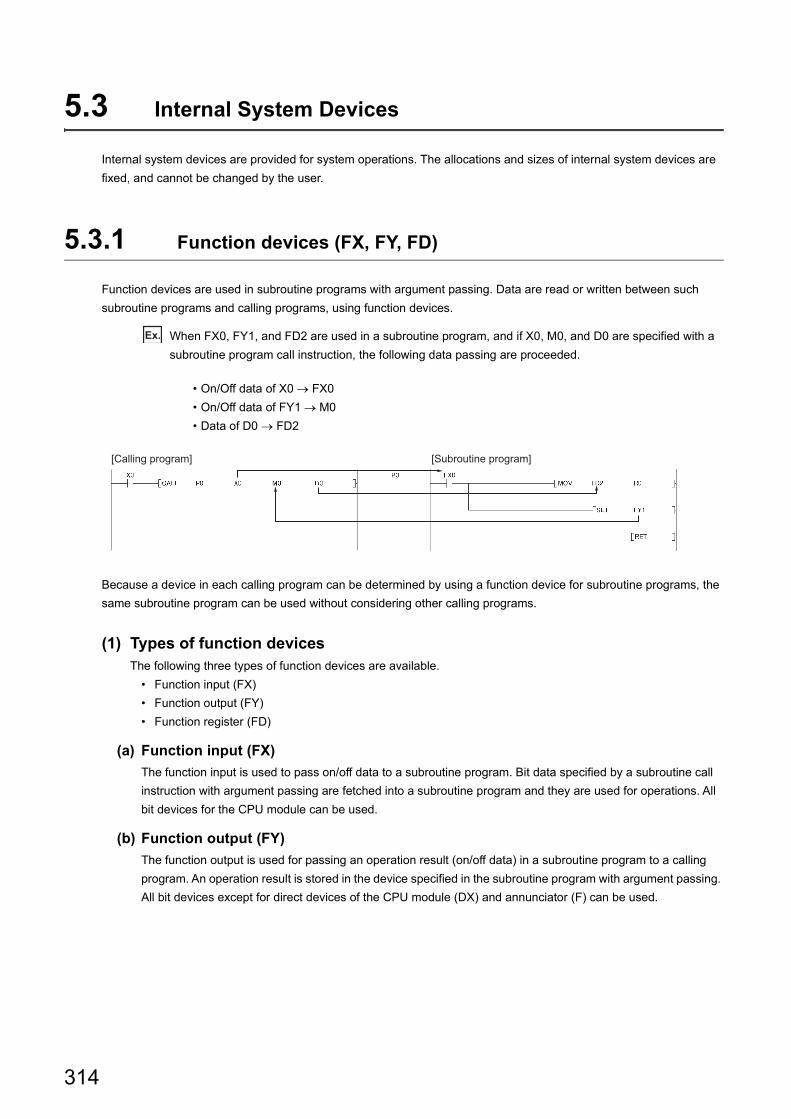
5.3 Internal System Devices
Internal system devices are provided for system operations. The allocations and sizes of internal system devices are
fixed, and cannot be changed by the user.
5.3.1 Function devices (FX, FY, FD)
Function devices are used in subroutine programs with argument passing. Data are read or written between such
subroutine programs and calling programs, using function devices.
Ex. When FX0, FY1, and FD2 are used in a subroutine program, and if X0, M0, and D0 are specified with a
subroutine program call instruction, the following data passing are proceeded.
Because a device in each calling program can be determined by using a function device for subroutine programs, the
same subroutine program can be used without considering other calling programs.
(1) Types of function devicesThe following three types of function devices are available.
• Function input (FX)
• Function output (FY)
• Function register (FD)
(a) Function input (FX)
The function input is used to pass on/off data to a subroutine program. Bit data specified by a subroutine call
instruction with argument passing are fetched into a subroutine program and they are used for operations. All
bit devices for the CPU module can be used.
(b) Function output (FY)
The function output is used for passing an operation result (on/off data) in a subroutine program to a calling
program. An operation result is stored in the device specified in the subroutine program with argument passing.
All bit devices except for direct devices of the CPU module (DX) and annunciator (F) can be used.
• On/Off data of X0 FX0
• On/Off data of FY1 M0
• Data of D0 FD2
[Calling program] [Subroutine program]
314

CHAPTER 5 DEVICES
5
5.3
Inte
rna
l Syste
m D
evice
s5
.3.1
Fu
nctio
n d
evice
s (FX
, FY
, FD
)
(c) Function register (FD)
The function register is used for data writing or reading between a subroutine program and a calling program.
The CPU module auto-detects the input or output conditions of the function register. Source data are input data
of the subroutine program. Destination data are output data of the subroutine program. The function register of
one point can occupy up to four words. Note that, however, the number of words used differs depending on the
instruction in the subroutine program.
• A one-word instruction uses one word only.
• A two-word instruction uses two words.
• At a destination using 32-bit multiplication or division, four words are used.
• Word devices of the CPU module can be used.
In subroutine programs with argument passing, do not use any devices that are used by the function register.If this occurs, function register values will not be normally passed to the calling program.
Data are stored in D0 (1 point).
Data are stored in D0 and D1 (2 points).
Data are stored in D0 to D3 (4 points).
Since D0 to D3 are used for FD0, D3 cannot be
used in the subroutine program.
315

5.3.2 Special relay (SM)
The special relay (SM) is an internal relay of which details are specified inside the CPU module, and the CPU module
status data are stored in this special relay.
MELSEC-L CPU Module User's Manual (Hardware Design, Maintenance and Inspection)
5.3.3 Special register (SD)
The special register (SD) is an internal register of which details are specified inside the CPU module, and the CPU
module status data (such as failure diagnostics or system information) are stored in this special register.
MELSEC-L CPU Module User's Manual (Hardware Design, Maintenance and Inspection)
316

CHAPTER 5 DEVICES
5
5.4
Lin
k Dire
ct De
vices
5.4 Link Direct Devices
The link direct device allows direct access to the link device of the CC-Link IE Field Network master/local module.
Regardless of the link refresh of the CPU module, the direct reading/writing from/to the link device of the CC-Link IE
Field Network master/local module can be done by using a program.
(1) Specification methodSpecify by the following network number and device No.
(2) Application example"J2\W10" is for the network No.2 and the link register 10 (W10).
For the bit device (X, Y, B, SB), specify by the digit.
Ex. J1\K1X0, J10\K4B0
Specification method: J \
Device No.
Link input (RX) X0 to 3FFF
Link output (RY) Y0 to 3FFF
Link register (RWw) W0 to 1FFF
Link register (RWr) W2000 to 3FFF
Link special relay (SB) SB0 to 1FF
Link special register (SW) SW0 to 1FF
Network number 1 to 239
K100 J2\W10MOVP
LW 0
LW10
CC-Link IE Field
Network master/local
module of network
number 2
317

(3) Specification rangeThe link devices, which are out of the range specified by the refresh parameter, can be specified.
(a) Writing
Write data within the link device range, which is set as the send range in the Common Parameter of the
network parameter and out of the refresh range of the refresh parameter
Although the writing within the link device range, which is set as the refresh range in the Refresh Parameter,
can be done, the data of link device in the link module will be rewritten when a refresh occurs. When write to
the link device by using the link direct device, write the same data to the corresponding device of the CPU
module, which is set in the Refresh Parameter.
Ex. Writing to the link device which is set as the refresh range
[Settings of the refresh parameter]
When the writing by the link direct device is done in the write range of the other station, the data will be
replaced with the received data during the data reception from the other station.
• Network number: 1
• Device of the CPU module: W0 to 3F
• Device of the CC-Link IE Field Network master/local module: SW0 to 3F
SB 0W 0
CPU module
Refresh range
Write range
Send range
Link range
CC-Link IE Field Network
master/local module
MOV K100 W1
MOV K100
W0W1 SW1
W1
MOV J1\SW1
MOV J1\SW1W1
W1
[Program]
[Writing timing]CPU module
Writing at
instruction
execution
Writing at instruction
execution
Writing by a refresh
CC-Link IE Field Network
master/local module
"100" is written to CC-Link IE Field
Network master/local module SW1 when
a refresh occurs.
"100" is written to CC-Link IE Field
Network master/local module SW1 when
the MOV instruction is executed.
318

CHAPTER 5 DEVICES
5
5.4
Lin
k Dire
ct De
vices
(b) Reading
The reading of the link device range of the CC-Link IE Field Network master/local module can be done.
The writing/reading by the link direct device can be done only for a single CC-Link IE Field Network
master/local module per network number. For instance, when more than two CC-Link IE Field Network
master/local modules are connected with the same network number, the writing/reading by the link direct
device can be done only for the network module with the smaller slot number.
Ex. When the CC-Link IE Field Network master/local modules (Station No.1 and Station No.2) are connected
as Network No.1 as shown below, the usage of the link direct device is allowed only for the network
module of Station No.2.
(4) Difference between the link direct device and the link refreshThe following table shows the difference between the link direct device and the link refresh
Remark
For the network parameters, common parameters, and refresh parameters, refer to the following.MELSEC-L CC-Link IE Field Network Master/Local Module User's Manual
Item Link direct device Link refresh
Notation in the program
Link register J\W0 to W0 to
Link special relay J\SB0 to SB0 to
Link special register J\SW0 to SW0 to
Number of steps 2 steps 1 step
Access range of the CC-Link IE Field Network master/local
moduleJ\0 to 3FFF
The range that is set in the
Refresh Parameter
Guaranteed range of access data 2 words (32 bits) unit
Network No.1
Writing/reading using link
direct devices allowed
StationNo.1
StationNo.2
Writing/reading using link
direct devices not allowed
319

5.5 Module Access Devices
5.5.1 Intelligent function module device
The intelligent function module device allows direct access from the CPU module to the buffer memories of the
connected intelligent function modules.
(1) Specification methodSpecify the I/O number and buffer memory address of the intelligent function module.
(2) Application exampleWhen the L60AD4 high-speed analog-digital converter module is connected in the position of the start I/O
number X/Y050, specify the device as shown below to store digital output values of CH.1 to CH.4 into D0 to D3
accordingly.
If the intelligent function module device is used, device comments can be attached to the buffer memory.Operating manual for the programming tool used
Specification method:
Buffer memory address (setting range: 0 to 65535 in decimal)
X/Y1F0 X/Y1F0
Start I/O number of intelligent function module
Specification: 1F
Setting: First 2 digits of start I/O number expressed with 3 digits
Setting range: 00H to FFH
U \G
L60AD4
12
13
11
14
CH1 Digital output value
CH2 Digital output value
CH3 Digital output value
CH4 Digital output value
320

CHAPTER 5 DEVICES
5
5.5
Mo
du
le A
ccess D
evice
s5
.5.1
Inte
llige
nt fu
nctio
n m
od
ule
de
vice
(3) Processing speedThe processing speed of the intelligent function module device is as follows:
• The processing speed of writing or reading using the intelligent function module device is slightly higher
compared with the case of using the FROM or TO instruction. (Example: "MOV U5\G11 D0")
• When reading from the buffer memory of an intelligent function module and another processing with one
instruction, totalize the processing speed of the FROM or TO instruction and the other instruction. (Example:
"+ U5\G11 D0 D10")
Instead of using the intelligent function module device in the program more than once to write or read buffer memory data, use the FROM or TO instruction once in one place so that the processing speed increases.
For the buffer memory address and application, refer to the manual for the intelligent function module used. For
the FROM or TO instruction, refer to the following.
MELSEC-Q/L Programming Manual (Common Instruction)
Writes data once in the program
Writes data to a device
such as data register (D)
321

5.6 Index Register/Standard Device Register (Z)
5.6.1 Index Register (Z)
The index register is used for indirect specification (index modification) in programs. Index modification uses one point
of the index register.
The index register has 20 points (Z0 to Z19).
(1) Bit structure of the index registerOne point of the index register consists of 16 bits, and data can be read or written in units of 16 bits.
Link register data are handled as signed data. In the case of the hexadecimal notation, 0000H to FFFFH can be stored.
However, because the most significant bit represents a sign bit, decimal values that can be specified are -32768 to 32767. (When using T, TS, or C device, specify the values within the range of -16384 to 16383.)
(2) Using in a 32-bit instructionThe processing target is Zn and Zn+1. The lower 16 bits correspond to the specified index register number (Zn),
and the higher 16 bits correspond to the specified index register number + 1.
Ex. When Z2 is specified in the DMOV instruction, Z2 represents the lower 16 bits and Z3 represents the
higher 16 bits. (The most significant bit in a 32-bit structure is a sign bit.)
Specify the index register by one point
(16 bits).
Zn
b15 to b0
The most significant bit is a sign bit.
Z3
Lower 16 bits Upper 16 bits
Z2
Processing target: Z2, Z3
322

CHAPTER 5 DEVICES
5
5.6
Ind
ex R
eg
ister/S
tan
da
rd D
evice
Re
giste
r (Z)
5.6
.2 S
tan
da
rd d
evice
reg
ister (Z
)
(3) When using 32-bit index modificationFor the file register (ZR), extended data register (D), extended link register (W) using the serial number access
method, 32-bit index modification using two points of the index register is available.
The following two kinds of methods can be used to specify the index register.
• Specify the range used for 32-bit index modification.
• Specify the 32-bit index modification using "ZZ".
For details on specification of the index register, refer to the following.
MELSEC-Q/L Programming Manual (Common Instruction)
5.6.2 Standard device register (Z)
By using the index register between register operations, operations can be executed at a higher speed. The index
register used in this case is called the standard device resister.
MELSEC-Q/L Programming Manual (Common Instruction)
(1) Device numberSince the standard device register is the same device as the index register, pay attention not to use the same
device number when using the index modification.
323

5.6.3 Saving and restoration of the index register
The CPU module performs the following when switching from the scan execution type program to the interrupt/fixed
scan execution type program.
• Saving and restoring the index register data
• Saving and restoring block numbers of the file register
(1) Setting for saving and restorationConfigure the setting for saving and restoration using a programming tool.
Project window [Parameter] [PLC Parameter] [PLC System]
When not writing data to the index register during interrupt/fixed scan execution type program, select "High
Speed Execution" in the Interrupt Program/Fixed Scan Program Setting area. This setting enables faster program
switching because saving and restoration are not performed.
(2) Processing of the index register
(a) When "High speed execution" is not selected
*1 The Z0 value is changed to 3 in the interrupt program.
To pass index register values from the interrupt/fixed scan execution type program to the scan execution type program, use word devices.
Selecting this
saves or restores
index register data.
Execution program
Z0 = 1 Z0 = 1 Z0 = 3
Z0 = 0 Z0 = 1
Passed
Switching
Saved
Restored
Restored
Z0 = 1 Z0 = 1 Z0 = 1
Z0 = 1
Index register save area
Index register value
Scan execution
type program
Scan execution
type program
Interrupt/fixed
scan execution
type program
for scan execution
type program
1) The CPU module saves the index register
values and passes them at program
switching.
2) The CPU module restores the index
register values saved at program switching.
*1
324

CHAPTER 5 DEVICES
5
5.6
Ind
ex R
eg
ister/S
tan
da
rd D
evice
Re
giste
r (Z)
5.6
.3 S
avin
g a
nd
resto
ratio
n o
f the
ind
ex re
giste
r
(b) When "High Speed Execution" is selected
*1 The Z0 value is changed to 3 in the interrupt program.
When writing data to the index register, use the ZPUSH or ZPOP instruction to save and restore the data. ( MELSEC-Q/L Programming Manual (Common Instruction))
(3) Processing of file register block numbers
Execution program
Z0 = 1
Z0 = 0
Switching Restored
Passed Passed
Z0 = 0 Z0 = 0 Z0 = 0 Z0 = 0
Z0 = 3Index register value
Save area of index register
for scan execution
type program
Scan execution
type program
Interrupt/fixed
scan execution
type program
Scan execution
type program
1) The CPU module does not save index register
values at program switching.
2) If data are written to the index register, the values of
the index register used in the scan execution type program
will be corrupted at program switching.
Z0 = 1 Z0 = 3
*1
3) The index register
values are not saved.
[RSET K0]
Execution program
Save area
Switching Restored
Block 1
Restored
Block 1Block 1Block 1 Block 1Block 0
Block 1Passed
SavedBlock 1 0
Block No. of
file register
Scan execution
type program
Scan execution
type program
Interrupt/fixed
scan execution
type program
1) The CPU module saves the block numbers of
the file register and passes them at program
switching.
2) The CPU module restores the block
numbers of the file register saved at
program switching.
325

5.7 File Register (R, ZR)
These device are provided for extending the data register.
(1) Specification methodsThe following two methods are available.
• Block switching method (R)
• Serial number access method (ZR)
(a) Block switching method (R)
The file register points used are divided and specified in units of 32K points (R0 to R32767).
When multiple blocks are used, the desired block is specified with the block number by the RSET instruction.
(b) Serial number access method (ZR)
A file register exceeding 32K points in size can be specified using consecutive device numbers.
Multiple blocks of a file register can be used as a continuous file register.
12K pointsData register
D0
12K pointsData register
D0
Data register can be
extended.
R0
File register
Block 0
Block 1
Block 2
R0
R0
R32767
R32767
R0R0 specification
for block 1
R0 specification
for block 2
......
...
ZR0
ZR32767ZR32768
ZR65535ZR65536
(Block 0)
(Block 1)
(Block 2)
......
...
326
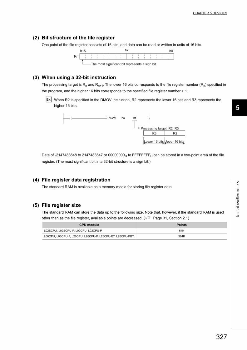
CHAPTER 5 DEVICES
5
5.7
File
Re
giste
r (R, Z
R)
(2) Bit structure of the file registerOne point of the file register consists of 16 bits, and data can be read or written in units of 16 bits.
(3) When using a 32-bit instructionThe processing target is Rn and Rn+1. The lower 16 bits corresponds to the file register number (Rn) specified in
the program, and the higher 16 bits corresponds to the specified file register number + 1.
Ex. When R2 is specified in the DMOV instruction, R2 represents the lower 16 bits and R3 represents the
higher 16 bits.
Data of -2147483648 to 2147483647 or 00000000H to FFFFFFFFH can be stored in a two-point area of the file
register. (The most significant bit in a 32-bit structure is a sign bit.)
(4) File register data registrationThe standard RAM is available as a memory media for storing file register data.
(5) File register sizeThe standard RAM can store the data up to the following size. Note that, however, if the standard RAM is used
other than as the file register, available points are decreased. ( Page 31, Section 2.1)
CPU module Points
L02SCPU, L02SCPU-P, L02CPU, L02CPU-P 64K
L06CPU, L06CPU-P, L26CPU, L26CPU-P, L26CPU-BT, L26CPU-PBT 384K
Rn
b15 to b0
The most significant bit represents a sign bit.
R3
Lower 16 bits Upper 16 bits
R2
Processing target: R2, R3
327

(6) Setting method
(a) File register setting
When using a file register, select "Use the following file". (Set in the same way when using an extended data
register (D) or an extended link register (W).)
Project window [Parameter] [PLC Parameter] [PLC File]
*1 The total points of the file register (ZR), extended data register (D), and extended link register (W).
When using the file register, it is shared by all the programs to be executed. A file register file is created after the parameters specified in "Corresponding Memory" and "File Name" are written to the CPU module. When the capacity is not specified, note the following.
• When the specified file register file is stored in the specified drive, the file is used. (The capacity is the same as that of the stored file register file.)
• If the file register file with the specified file name is not found in the specified drive, "PARAMETER ERROR" (error code: 3002) occurs.
(b) Device setting
The points of the file register (ZR) can be set in the File Register Extended Setting.
Project window [Parameter] [PLC Parameter] [Device]
1. The latch range can be changed if necessary.
• Latch (2) of the file register (ZR)
CPU moduleCorresponding
memoryFile name Capacity*1
L02SCPU, L02SCPU-P, L02CPU, L02CPU-P
Standard RAM Any name
1 to 64K points
L06CPU, L06CPU-P, L26CPU, L26CPU-P, L26CPU-BT,
L26CPU-PBT1 to 384K points
Select "Use the following file".
The number of file register points set in
the PLC file tab is displayed.
Specify the latch range.
When using an extended data register (D) and an
extended link register (W), set the device points so
that the total is equal to the file register capacity
set in the PLC file tab.
328

CHAPTER 5 DEVICES
5
5.7
File
Re
giste
r (R, Z
R)
(7) Clearing the file registerIf the Latch (2) is set in the Device tab of the PLC parameter dialog box, the data in the file register are not
cleared even if the CPU module is powered off or reset. (Data cannot be cleared by performing a latch clear
operation.*1)
For how to clear the data, refer to the "Latch data clear" section. ( Page 89, Section 3.4 (4))
*1 The latch range of the file register can be set in the Device tab of the PLC Parameter dialog box. ( Page 328, Section 5.7 (6) (b))
(8) Deleting a file register fileOpen the "Online Data Operation" dialog box.
[Online] [Delete PLC Data...]
(9) Precautions
(a) If the file register number not registered is used
If a file register file is not registered and writing to or reading from the file register is performed, "OPERATION
ERROR" (error code: 4101) occurs.
(b) If writing to or reading from the file register is performed exceeding the registered
size of points
"OPERATION ERROR" (error code: 4101) occurs.
(c) File register size check
When writing to or reading from the file register, check the file register size so that data can be written or read
within the size (points) set for the CPU module. Check the file register size at step 0 in the program if any file
register is used.
The file register size can be checked in SD647.
Before executing a file register block switching instruction (RSET), ensure that 1K points or more of space are
secured after the switching.
(File register size) > [32K points (Switching block No.) + 1K points]
4K points specified
Transfer
command
Final file register
range check
Writing to the file
register
Alarm processing
Block switching command
Final file register
range check
Switching to block 1
Alarm processing
329

5.8 Extended Data Register (D) and Extended Link Register (W)
The extended data register (D) and extended link register (W) are devices for utilizing the large-capacity file register
(ZR) area as an extended area of the data register (D) and link register (W). These devices can be programmed as the
data register (D) and link register (W) together with the file register (ZR) area.
Device numbers for the extended data register (D) and extended link register (W) can be consecutively assigned after
those for the internal user devices, data register (D) and link register (W). Note that even though device numbers are
consecutively assigned, there is no physical area contiguity between the data register (D) (internal user device) and
the extended data register (D), and between the link register (W) (internal user device) and the extended link register
(W). To use them as one contiguous area, set the points for the data register (D) and link register (W) (internal user
device) to "0" in the Device tab of the PLC Parameter dialog box, and use only the extended data register (D) and
extended link register (W).
When using the file register (ZR), extended data register (D) and extended link register (W) with the auto refresh setting for the intelligent function module, the points set in the File register extended setting in the Device tab of the PLC Parameter dialog box must not be exceeded.
Device numbers can be assigned to the data register and extended data register consecutively.
The file size is the total number of points for thefile register, extended data register, and extended link register.
D0
ZR
D12287
D12287D12288
ZR210943D12288
D63487W2000
D0
D63487
Device
Data register
Extended dataregister
Points for data register
Internal user device
File register file
Pointsfor file register
Points for extended data registers
Points for extended link registers
330
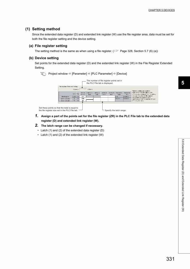
CHAPTER 5 DEVICES
5
5.8
Exte
nd
ed
Da
ta R
eg
ister (D
) an
d E
xten
de
d L
ink R
eg
ister (W
)
(1) Setting methodSince the extended data register (D) and extended link register (W) use the file register area, data must be set for
both the file register setting and the device setting.
(a) File register setting
The setting method is the same as when using a file register. ( Page 328, Section 5.7 (6) (a))
(b) Device setting
Set points for the extended data register (D) and the extended link register (W) in the File Register Extended
Setting.
Project window [Parameter] [PLC Parameter] [Device]
1. Assign a part of the points set for the file register (ZR) in the PLC File tab to the extended data
register (D) and extended link register (W).
2. The latch range can be changed if necessary.
• Latch (1) and (2) of the extended data register (D)
• Latch (1) and (2) of the extended link register (W)
The number of file register points set in
the PLC File tab is displayed.
Specify the latch range.
Set these points so that the total is equal to
the file register size set in the PLC File tab.
331

Once the points for the extended data register (D) and extended link register (W) is set, areas for these devices
are reserved in the file register file.
The points for each of the file register (ZR), extended data register (D), and extended link register (W) can be
checked in the following SD.
SD number Corresponding points
SD306, SD307 File register (ZR)
SD308, SD309 Data register (D) + Extended data register (D)
SD310, SD311 Link register (W) + Extended link register
Actual area
Internal user device
D0
D12287
File register file
ZR0
ZR20479
D12288
D53247
W2000
Points for
file register
Points for
extended
data register
Points for
extended
link register
Areas for the points for extended data register and extended link register are reserved in this order, after the area for the points for file register.
Device
Data register
Extended
data register
D12287
D12288
D0
D53247
Points for data
register
332

CHAPTER 5 DEVICES
5
5.8
Exte
nd
ed
Da
ta R
eg
ister (D
) an
d E
xten
de
d L
ink R
eg
ister (W
)
(2) Precautions
(a) Specifying the extended data register (D) and extended link register (W)
Since the file register (ZR) area is used, the values of the following items will be the same as those for the file
register (ZR).
• Number of program steps
• Instruction processing time
• Link refresh time with the CC-Link IE Field Network master/local module
• Link refresh time with CC-Link IE Field Network Basic
• Auto refresh time with CC-Link
• Processing time of auto refresh with intelligent function modules
(b) Changing the file register size
The file register size cannot be changed while the CPU module is in the RUN status.
(c) Refresh range
Set the refresh ranges for the following auto refresh properly so that each refresh range does not cross over
the boundary between the internal user device and the extended data register (D) or extended link register (W).
• Link refresh with CC-Link IE Field Network
• Link refresh with CC-Link IE Field Network Basic
• Auto refresh with CC-Link
• Refresh with intelligent function modules
(d) Specifying in a program
Set the following properly so that each specification does not cross over the boundary between the internal
user device and the extended data register (D) or extended link register (W).
• Index modification
• Indirect specification
• Specification for instructions that use block data*1
*1 Block data means the following: Data used in instructions, such as FMOV, BMOV, and BK+, which treat more than one word for operation Control data, composed of two or more words, which are specified in instructions, such as SP.FWRITE and SP.FREAD. Data in a 32-bit or greater format (binary 32 bits, real number, indirect address of a device)
For details on the index modification and indirect specification with the extended data register (D) and extended
link register (W), refer to the following.
MELSEC-Q/L Programming Manual (Common Instruction)
333

(e) Access from an inapplicable module
To access the extended data register (D) or extended link register (W) from a module that does not support the
use of these devices, device numbers need to be specified with those of the file register (ZR). Calculation
formulas for obtaining device numbers of the file register (ZR) to be specified and calculation examples are
described below
*1 Variables in the table indicate the following: ZRC: Points of the file register (ZR)
EDZN: Device number of the file register (ZR) used to access the extended data register (D)
EDN: Access target device number of the extended data register (D)
EDC: Points of the data register (D)
EDC: Points of the extended data register (D)
EWZN: Device number of the file register (ZR) used to access the extended link register (W)
EWN: Access target device number of the extended link register (W) (hexadecimal)
EWC: Points of the link register (W)
[Calculation example]
• DC: Points of the data register (D) 12288 points
• WC: Points of the link register (W) 8192 points
• ZRC: Points of the file register (ZR) 2048 points
• EDC: Points of the extended data register (D) 2048 points
Ex. Device number of the file register (ZR) used to access D13000
EDZN = 2048 + (13000 - 12288) = 2760
Ex. Device number of the file register (ZR) used to access W2100
EWZN = 2048 + 2048 + (2100H - 8192) = 2048 + 2048 + (8448 - 8192) = 4352
Item Calculation method
Device number of the file register (ZR) used to access the extended data register (D) EDZN = ZRC + (EDN - DC)
Device number of the file register (ZR) used to access the extended link register (W) EWZN = ZRC + EDC + (EWN - WC)
Data register (D)
Extended data register (D)
Link register (W)
Extended link register (W)
File register (ZR)
ZR0
ZR2047
ZR2048
ZR2760
ZR4095
ZR4096
ZR4352
ZR6143
D0
D12287
D12288
1) D13000
D14335
W0
W1999
W2000
2) W2100
W27FF
334

CHAPTER 5 DEVICES
5
5.9
Ne
sting
(N)
5.9 Nesting (N)
Nesting (N) is a device used in the master control instructions (MC and MCR instructions) to program operation
conditions in a nesting structure. The master control instruction opens or closes a common ladder gate to efficiently
switch the ladder of a program. Specify the nesting (N) in ascending order (in order of N0 to N14), starting from the
outside of the nesting structure.
For use of the nesting, refer to the following.
MELSEC-Q/L Programming Manual (Common Instruction)
Executed when conditions A
and B are met.
Executed when conditions A,
B, and C are met.
Executed when conditions A
and B are met.
Executed when condition A is
met.
Executed when condition A is
met.
Specified in ascending order.
Specified in descending order.
Executed regardless of
conditions A, B, and C.
Control range
of nesting
N0
Control range
of nesting
N1
Control range
of nesting
N2
335

5.10 Pointer (P)
The pointer (P) is a device used in jump instructions (CJ, SCJ, or JMP) or subroutine call instructions (such as CALL).
Pointers can be used in the following applications.
• Specification of the jump destination in a jump instruction (CJ, SCJ, or JMP) and a label (start address of the
jump destination)
• Specification of the call destination of a subroutine call instruction (CALL or CALLP) and a label (start
address of the subroutine program)
There are the following two different pointer types.
The number of points available for the pointer is 4096.
For the L06CPU, L06CPU-P, L26CPU, L26CPU-P, L26CPU-BT, L26CPU-PBT with a serial number of "16042" or later, the pointer for auto assignment device can be used up to 32768 points by using GX Works2. (The PC parameters should be set. ( Page 362, Appendix 1.2 (8)))
For the jump instructions and subroutine call instructions, refer to the following.
MELSEC-Q/L Programming Manual (Common Instruction)
• Local pointer:
The pointer used independently in each program
• Common pointer:
The pointer that can be called in all running programs by the subroutine call instruction.
336

CHAPTER 5 DEVICES
5
5.1
0 P
oin
ter (P
)5
.10
.1 L
oca
l po
inte
r
5.10.1 Local pointer
The local pointer is a pointer that can be used independently in jump instructions and subroutine call instructions in
each program. The same pointer number can be used in respective programs.
The local pointer can be divided for use of all the programs stored in the program memory. The local pointer number
ranges from P0 to the highest number of the local pointer in use. (The CPU module's system computes the number of
points used.)
Even if only P99 is used in a program, for example, the number of points used will be 100, which is from P0 to P99. For
using the local pointer for several programs, use the pointers in ascending order starting from P0 in each program.
Ex. The total is 600 points when the pointer is used as shown below.
● When the program where the local pointer is described, the program cannot jump in from another program is not allowed. Use the ECALL instruction from another program when calling a subroutine program in a program file that contains any local pointer.
● If the total number of pointers (in all programs) exceeds 4096 points, a "CAN'T SET (P)" (error code: 4020) occurs.
Program BProgram A
The same pointer
No. can be used.
100 points of P0 to
P99 occupied200 points of P0 to
P199 occupied
300 points of P0 to
P299 occupied
Program A Program B Program C
Using P0 to P99 Using P100 to P199 Using P299 only
Use of P0 to P99 occupies 100 points.
Use of P0 occupies 1 point.
Total of 600 points
are used.
337

5.10.2 Common pointer
The common pointer is used to call subroutine programs from all programs that are being executed.
To set the common pointer range, enter the start number of the common pointer. The common pointer range is from
the specified pointer number to P4095. However, the pointer number that can be entered here is a number greater
than the total points used for the local pointer.
Project window [Parameter] [PLC Parameter] [PLC System]
Ex. If a total of 400 points are used in three programs (100 points in each of Program A and Program B, and
200 points in Program C), for example, P400 and higher numbers can be set for the common pointer.
● The same pointer number cannot be used as a label. If used, "CAN'T SET(P)" (error code: 4021) occurs.
● If the total number of the local pointer points used in several programs exceeds the start number of the common pointer, a "CAN'T SET (P)" (error code: 4020) occurs.
● The jump instructions are not capable of executing a jump to the common pointer in other programs. Use the common pointer with subroutine call instructions only.
Program A Program C
Program B
Label
Set the start number for
the common pointer.
100 points of P0 to
P99 occupied
100 points of P0 to
P99 occupied
200 points of P0 to
P199 occupied
Program A Program B Program C
Total of 400 points
are used.
Using P0 to P99 Using P0 to P99 Using P0 to P199
P400 and higher numbers can be
used for the common pointer.
338

CHAPTER 5 DEVICES
5
5.1
1 In
terru
pt P
oin
ter (I)
5.11 Interrupt Pointer (I)
The interrupt pointer (I) is used as a label at the start of an interrupt program, and can be used in any programs.
The number of points available for the interrupt pointer is 256 (I0 to I255). The following shows interrupt factors for the
applicable interrupt pointers.
*1 Interrupt pointer numbers can be changed in the PLC Parameter dialog box.*2 They can be used for interruptions by built-in I/O by configuring parameter in the "PLC Parameter" dialog box.
To use the intelligent function module interrupt, set values in the "Interrupt Pointer Setting" dialog box opened from the "PLC System" tab of the PLC Parameter dialog box. ( Page 354, Appendix 1.2 (2))
The list of interrupt pointer numbers and interrupt factors are shown below.
*1 The time-limit value of the internal timer is set by default. In the PLC System tab of the PLC Parameter dialog box, the value can be changed within the range of 2ms to 1000ms in increments of 1ms.
*2 When an interrupt occurs, even if no interrupt pointer exists on the program, "CAN'T EXECUTE(I)" (error code: 4220) does not occur.
*3 Among I50 to I255, I50 has the highest priority (priority 21), and I255 has the lowest priority (priority 226).
Interrupt factorInterrupt pointer
No.Description
Interrupt by built-in I/O I0 to I15*1 Interrupt from a built-in I/O
Interrupt by an internal timer I28 to I31Interrupt at fixed intervals by an internal timer of the CPU
module
Intelligent function module interrupt I50 to I255*2 Interrupt from the intelligent function module
I No. Interrupt factor Priority I No. Interrupt factor Priority
I0
Interrupt by built-in I/O
1st point 5
I16 to I27 Empty
I1 2nd point 6
I2 3rd point 7
I3 4th point 8
I4 5th point 9
I5 6th point 10
I6 7th point 11 I28
Interrupt by internal
timer*1*2
100ms 4
I7 8th point 12 I29 40ms 3
I8 9th point 13 I30 20ms 2
I9 10th point 14 I31 10ms 1
I10 11th point 15 I32 to I49 Empty
I11 12th point 16
I50 to I255Intelligent function
module interruptEmpty 21 to 226*3
I12 13th point 17
I13 14th point 18
I14 15th point 19
I15 16th point 20
Interrupt pointer (interrupt program label)
Interrupt program
339

5.12 Other Devices
5.12.1 SFC block device (BL)
The SFC block is used to check that the specified block in the SFC program is activated.
MELSEC-Q/L/QnA Programming Manual (SFC)
5.12.2 I/O No. specification device (U)
The I/O No. specification device is used to specify I/O numbers in the intelligent function module dedicated
instructions. The following shows how to specify the device.
For details on the intelligent function module dedicated instructions, refer to the following.
Manual for the intelligent function module used
UnGP.READ S1 S2 S3 D
Instruction name
I/O No. specification instruction
I/O No. specification device
(n: I/O No.)
340

CHAPTER 5 DEVICES
5
5.1
2 O
the
r De
vices
5.1
2.3
Ma
cro in
structio
n a
rgu
me
nt d
evice
(VD
)
5.12.3 Macro instruction argument device (VD)
The macro instruction argument device (VD) is used with ladders registered as macros. When a VD setting is
specified, the value is converted to the specified device when the macro instruction is executed. With the macro
instruction argument device, VD0 to VD9 can be used in one macro registration ladder.
Among the devices used in the ladders registered as macros, specify a device used for VD. When using macro
instructions in the program, specify devices that correspond to the macro instruction argument devices used in the
macro registration ladders in ascending order.
Passing to VD2VD0MOV VD2VD0> VD1D0M.MAX D1 R0
Passing to VD1
Passing to VD0
VD1MOV VD2VD0< = VD1
Command with the name of the ladder registered as a macro
Program that actually runs in the CPU module
Program
Ladder registered as a macro
(registration name: MAX)
D0MOV R0D0> D1
D1MOV R0D0< = D1
341

CHAPTER 6 CONSTANTS
The following constants can be used in the CPU module.
• Decimal constant (K)
• Hexadecimal constant (H)
• Real number (E)
• Character string (" ")
6.1 Decimal Constant (K)
The decimal constant (K) is a device used to specify decimal data in programs. Specify it as K (example: K1234) in
programs. In the CPU module, data are stored in binary (BIN). ( Page 389, Appendix 4)
The specification ranges for decimal constants are as follows:
The most significant bit represents a sign bit.
• When using word data (16-bit data): K-32768 to K32767
• When using 2-word data (32-bit data): K-2147483648 to K2147483647
6.2 Hexadecimal Constant (H)
The hexadecimal constant (H) is a device used to specify hexadecimal or BCD data in programs. (For BCD data, each
digit of a hexadecimal number is specified with 0 to 9.) In programs, specify it as H (example: H1234). ( Page
389, Appendix 4)
The specification ranges for hexadecimal constants are as follows:
• When using word data (16-bit data): 0000H to FFFFH (For BCD data, 0000H to 9999H)
• When using 2-word data (32-bit data): 00000000H to FFFFFFFFH (For BCD data, 00000000H to 99999999H)
342

CHAPTER 6 CONSTANTS
6
6.3
Re
al N
um
be
r (E)
6.3 Real Number (E)
The real number (E) is a device used to specify real numbers in programs. In programs, specify it as E (example:
E1.234).
( Page 374, Appendix 1.3)
(1) Specification range
(a) Real number setting range
• For single-precision floating-point data
• For double-precision floating-point data*1
*1 Up to 15 digits can be entered in a programming tool.
(b) When an overflow or underflow has occurred
(c) When a special value*1 is input
If operation is performed with input data that contains a special value, "OPERATION ERROR" (error code:
4140) occurs.
*1 The special values are -0, unnormalized numbers, nonnumeric characters, and .
(2) Specification methodReal numbers can be specified in programs by the following expressions.
• Normal expression: A numeric value can be specified as it is. (Example: 10.2345 can be specified as
E10.2345.)
• Exponential expression: A numeric value is specified by (Value) 10n. (Example: 1234 is specified as
E1.234 + 3.*1)
*1 + 3 represents 103 in E1.234 + 3.
6.4 Character String (" ")
The character string is a device used to specify a character string in program. Characters enclosed in quotation marks
are specified. Alphabets are case-sensitive. A string from the specified character to the NUL code (00H) is one unit.
Note that, however, up to 32 characters can be specified for an instruction using a character string, such as $MOV.
-2128 < Device -2-126, 0, 2-126 Device < 2128
-21024 < Device -2-1022, 0, 2-1022 Device < 21024
Overflow Underflow
OPERATION ERROR (error code: 4141) Turned to 0 without any error
343

CHAPTER 7 CONVENIENT USAGE OF DEVICES
When multiple programs are executed in the CPU module, each program can be executed independently by specifying
an internal user device as a local device. Devices of the CPU module are classified into the following two types:
• Global device that can be shared by multiple programs that are being executed.
• Local device that is used independently for each program.
7.1 Global Device
Programs being executed in the CPU module can share the global device. Global device data are stored in the device
memory of the CPU module, and can be shared by all programs.
● All of the devices that have not been set as local devices ( Page 345, Section 7.2) are global devices.
● For execution of multiple programs, the range to be shared by all programs and the range to be used independently by each program must be specified in advance. ( Page 345, Section 7.2)
Program A
Program B
ON/OFF data of M0
Device memory
Internal relay
ON/OFFM0
ON/OFF data of M0
Example: Internal relay
M0 Shared by all programs.
Used in program A.
Used in program B.
Used in program C.
The ranges must be specified for each program.
344

CHAPTER 7 CONVENIENT USAGE OF DEVICES
7
7.2
Lo
cal D
evice
7.2 Local Device
The local device is a device that can be used independently for each program. Using local devices allows
programming of multiple independently-executed programs without considering other programs. Note that local device
data can be stored in the standard RAM only.
Ex. If M7000 and higher portion is set as a local device, it can be separately used for each program that is
executing M7000 and higher portion.
The following devices can be used as local devices.
After program execution, data in the local device file of the standard RAM are exchanged with the data in the device
memory of the CPU module. For this reason, the scan time increases by the time for data exchange.
● There are some instructions for which a local device cannot be specified. For details, refer to the pages describing devices available for each instruction in the following manual.MELSEC-Q/L Programming Manual (Common Instruction)
● For the concept of the number of words used for the local devices, refer to Page 290, Section 5.2.
• Internal relay (M) • Counter (C) • Edge relay (V)
• Data register (D) • Timer (T, ST) • Index register (Z)
ON/OFFM7000
ON/OFFM7000
Program A
Program B
ON/OFF data of M7000
ON/OFF data of M7000
Standard RAM
For program A
For program B
Internal relay
Internal relay
Local device
Program A Program B Program C
Local device Local device
Restored Saved Restored Saved Restored
Program
For
program A
For
program B
For
program C
For
program A
For
program B
For
program C
For
program A
For
program B
For
program C
345

(1) Local device settingTo use a local device, perform the following procedure.
Note that the local device range is common to all programs, and cannot be changed for each program.
Ex. If a local device range is specified as MO to M100, this range setting applies to all programs that use the
local device.
● The 32-bit index modification range must not overlap with the local device setting range of the index register. If overlapped, 32-bit index modification values will be written over the local device values.
● If the size of the local device in the standard RAM is set to be changed while a sampling trace file is stored in the standard RAM, the sampling trace file will be cleared. To save the trace results, store them in a personal computer.
● All of the devices that have not been set as local devices are global devices.
1. Set a local device range.
Project window [Parameter] [PLC Parameter]
[Device]
2. Set a memory for storing the local device file and a
file name.
Project window [Parameter] [PLC Parameter]
[PLC File]
3. Write the parameters to the CPU module.
Program A Program B Program CM0
M100
Local device range is
common to all programs.Local
device
Local
device
Local
device
346

CHAPTER 7 CONVENIENT USAGE OF DEVICES
7
7.2
Lo
cal D
evice
(2) Setting a local device in units of programUse of the local device can be set for each program, and this function can reduce the scan time. Also, since the
area for saving and restoring data are not required for the programs not using a local device, the local device file
size can be reduced.
(a) Setting method
In addition to the setting in (1) in this section, click the "File Usability Setting" button, and specify the programs
that use the local devices.
Project window [Parameter] [PLC Parameter] [Program] [File Usability Setting]
(b) Precautions
Do not change or refer to the local device in a program for which the local device is set to "Not used". The
changed data are not held.
Program A
Program B
Program C
Program execution Local device file (.QDL)
Save/Restore
Save/Restore
Save/Restore
File size can be reduced since the saving or
restoring area for program B is not created.
For program A
For program C
Scan time decreases since saving/restoring
processing is not performed.
347

(3) Local devices when executing a subroutine programWhen executing a subroutine program, the local device in the file where the subroutine program is stored can be
used by ON/OFF of SM776.
(a) When SM776 is off
(b) When SM776 is on
(c) Precautions
• When SM776 is on, local device data area read out when a subroutine program is called, and the data are
saved after execution of the RET instruction. Because of this, the scan time is increased if one subroutine
program is executed with SM776 set to on.
• The on/off status of SM776 is set for each CPU module. It cannot be set for each file.
• If the on/off status of SM776 is changed during program execution, control is implemented according to
the information after the change.
SM776 Operation
OFF Perform operations with the local device that corresponds to the source file of the subroutine program.
ON Perform operations with the local device that corresponds to the file where the subroutine program is stored.
Local device area
for file name, ABC
Local device area
for file name, DEF
Execution of subroutine
program
Local device
writing/reading
File name: DEF
(Standby type program)File name: ABC
Subroutine program
Local device area
for file name, ABC
Local device area
for file name, DEF
Execution of subroutine
program
Local device
writing/reading
File name: DEF
(Standby type program)File name: ABC
Subroutine program
348

CHAPTER 7 CONVENIENT USAGE OF DEVICES
7
7.2
Lo
cal D
evice
(4) When executing an interrupt/fixed scan execution type programWhen the local device is used for an interrupt/fixed scan execution type program, turn on SM777 (Enable/disable
local device in interrupt program). The programs will not function properly if SM777 is turned off.* 1
*1 The index register set as the local device uses the local device area for the program executed before the interrupt/fixed scan execution type program, regardless of the on/off status of SM777.
Ex. Operation when SM777 is turned on with the following setting
(a) Precautions
• When SM777 is on, local device data are read out before execution of an interrupt/fixed scan execution
type program, and the data are saved after execution of the IRET instruction. Because of this, the scan
time is increased if one interrupt/fixed scan execution type program is executed with SM777 set to on.
• The on/off status of SM777 is set for each CPU module. It cannot be set for each file.
• For the local device monitoring, the target local device is monitored by switching the selection of
corresponding program manually. When SM777 is off, when an interrupt occurred immediate after the
switch processing, monitoring target local device is monitored. (The local device for the program executed
prior to the interrupt (the program immediate before END) is not monitored.)
(5) Clearing local device dataLocal device data are cleared by the either of the following.
• When the CPU module is powered off and then on or is reset.
• When the CPU module status is changed from STOP to RUN.
Local device data cannot be cleared from a programming tool.
Program name Execute type Local device
A Scan Not used
B Scan Used
C Scan Used
X Fixed Scan Used
(1)Uses the program X local device.
(2)When an interrupt/fixed scan execution type program is executed during the END processing, the local device for Program C, which was
executed before the END processing, is read out and saved. Thus, the END processing time increases by the time required for the read and
save.
A ENDC A BB C END
X XX
(1) (1)(2) (1)
Execution program
Local device
For X
For B
For C
For X
For C
For X
For B For B
For C
349

APPENDICES
Appendix 1 Parameter Setting
Appendix 1.1 List of parameter numbers
Each parameter number is the value that is stored in the special register (SD16 to SD26) when an error occurs in the
parameter settings. The following list indicates the parameter items and corresponding parameter numbers.
Parameter No. Parameter item Set in: Reference
0000H LabelPLC Name
0001H Comment
1000H Timer Limit Setting
PLC System
Page 299, Section
5.2.10
1001H RUN-PAUSE ContactsPage 112, Section
3.12
1002H Remote ResetPage 112, Section
3.12
1003H Output Mode at STOP to RUN Page 101, Section 3.7
1004H Floating-point operation Page 389, Appendix 4
1005H Common Pointer No.Page 338, Section
5.10.2
1006H Pointer Extended Setting for Automatic-Assign DevicePage 336, Section
5.10
1007H Points Occupied by Empty Slot Page 41, Section 2.2
1008H System Interrupt Setting Page 339, Section
5.11100AH Intelligent Function Module Setting (Interrupt Pointer Setting)
100CH Module Synchronization Page 91, Section 3.5
100DH A-PLC Compatibility Setting
100EH Serial communication functionPage 227, Section
3.38
1013H Service Processing Setting Page 94, Section 3.6
1014H Latch Data Backup Operation Valid ContactPage 175, Section
3.28
1016H Built-in Ethernet Port Setting Built-in Ethernet Port Setting
1017H PLC Module Change SettingPLC System
Page 182, Section
3.31
1018H Built-in CC-Link Setting
1019H Simple PLC Communication Setting Built-in Ethernet Port Setting
101AH Serial Communication Function
Adapter Serial Setting, Built-in
Serial Setting
Page 227, Section
3.38
101BH Predefined Protocol Support FunctionPage 215, Section
3.37
101CH GOT Connection
101DH FTP Client Setting
Built-in Ethernet Port Setting
101EH E-mail Setting
1030H CC-Link IEF
Basic Setting
Network Configuration Setting
1031H Refresh Setting
350

APPX
A
Ap
pe
nd
ix 1 P
ara
me
ter S
ettin
gA
pp
en
dix 1
.1 L
ist of p
ara
me
ter n
um
be
rs
1100H File Register
PLC File
Page 326, Section 5.7
1101H Comment File Used in a CommandPage 344, CHAPTER
7
1102H Initial Device Value Page 91, Section 3.5
1103H File for Local Device Page 345, Section 7.2
1104H Transfer to Standard ROM at Latch data backup operationPage 175, Section
3.28
1105H Device data storage filePage 180, Section
3.29
2000H Device Points
Device Page 88, Section 3.4
2001H Latch range (latch clear is enabled)
2002H Latch range (latch clear is disabled)
2003H Local variable
2004H Latch range extended devices (latch clear is enabled)
2005H Latch range extended devices (latch clear is disabled)
3000H WDT (Watchdog Timer) Setting
PLC RAS
Page 87, Section 3.3
3001H Error Check Page 166, Section
3.253002H Operating Mode When there is an Error
3003H Constant Scanning
PLC RAS
Page 85, Section 3.2
300AH Module Error History CollectionPage 171, Section
3.27
0400H Slot setting
I/O Assignment
Page 41, Section 2.2
0403H Error Time Output ModePage 103, Section 3.9
4004H Error Time Operation Mode
0405H I/O Response Time Page 102, Section 3.8
0409H Switch Setting
5001H*1 Valid Module During Other Station Access CC-Link IE Field Network
setting
Page 374, Appendix
1.35003H*1 Routing Parameter
7000H Program Setting Program Page 61, Section 2.8
8002H SFC Program Start Mode
SFC 8003H Start Conditions
8006H Output Mode When the Block is Stopped
9000H Number of modules on Ethernet
EthernetPage 374, Appendix
1.3
9N00H
Start I/O No.
Network No.
Group No.
Station No.
Operation Setting
9N01H Initial Setting
9N02H Open Setting
9N03H Router relay parameter
9N05H Station No. <-> IP information
9N06H FTP Parameters
9N07HE-mail Setting
9N08H News Setting
9N09H Interrupt Settings
9N04H Routing Parameters
Parameter No. Parameter item Set in: Reference
351

*1 "N" indicates the position of the module (counted from the first one) and "M" indicates the network type of the module.
A080H*1 Number of Modules Setting
CC-Link IE Field Network
setting
Page 374, Appendix
1.3
ANM0H*1 Network Setting
ANM1H*1 Refresh Parameter
ANM2H*1 Common Parameter
ANM3H*1 Intrinsic parameter
B000H Positioning and High-speed counter functions settings
Built-in I/O Function Setting
MELSEC-L CPU
Module User's Manual
(Built-In I/O Function)
B001H Input Signal Function Selection
B002H Output Signal Function Selection
B003H Input Response Time
B004H Interrupt Processing Condition
B005H Error Time Output Mode
B006H, B007H Axis1: Positioning Parameter
B008H Axis1: OPR Parameter
B009H Axis1: Positioning Data
B00AH, B00BH Axis2: Positioning Parameter
B00CH Axis2: OPR Parameter
B00DH Axis2: Positioning Data
B00EH CH1: Common setting
B00FH, B010H CH1: Operation Mode
B011H CH1: Frequency Measurement Mode
B012H CH1: Rotation Speed Measurement Mode
B013H CH1: Pulse Measurement Mode
B014H CH2: Common Setting
B015H, B016H CH2: Normal Mode Setting
B017H CH2: Frequency Measurement Mode
B018H CH2: Rotation Speed Measurement Mode
B019H CH2: Pulse Measurement Mode
C000H Number of Modules I/O Assignment Page 43, Section 2.2.2
CNM1H *1 Network Refresh Setting
CC-Link setting CNM2H
*1 Common Parameters
FE00H Parameters for the programming tool
Start I/O number
10Refresh Parameter
Intelligent function module
parameterPage 77, Section 2.11
Password Active Module Setting Remote passwordPage 375, Appendix
1.4
Parameter No. Parameter item Set in: Reference
352

APPX
A
Ap
pe
nd
ix 1 P
ara
me
ter S
ettin
gA
pp
en
dix 1
.2 P
LC
pa
ram
ete
rs
Appendix 1.2 PLC parameters
This section provides parameter setting screens and details of the setting items.
Note that parameter setting is not available for the grayed out items.
(1) PLC Name settingA label name and a comment for the CPU module are set. The settings are displayed in the list for the find CPU
function. ( MELSEC-L CPU Module User's Manual (Built-In Ethernet Function))
ItemParameter
No.Description Setting range Default Reference
Label 0000HSet a label (name, application) for the CPU
module.Up to 10 characters
Comment 0001H Set a comment for the CPU module label. Up to 64 characters
353

(2) PLC System settingParameters of the system required for use of the CPU module are set.
ItemParameter
No.Description Setting range Default Reference
Timer Limit
Setting
Low Speed
1000HSet the time limit for the low
speed timer or high speed timer.
1ms to 1000ms (in increments of
1ms)100ms Page 299,
Section
5.2.10High Speed0.01ms to 100.0ms (in increments
of 0.01ms)10ms
RUN-PAUSE
Contacts
RUN1001H
Set the contacts that control
RUN PAUSE of the CPU
module.
X0 to X1FFF Page 112,
Section 3.12PAUSE *1
Latch Data Backup Function 1014H
Set the valid contact device No.
used for backup of latch data to
the standard ROM.
X, M, B Page 175,
Section 3.28
Remote Reset 1002HSelect whether to allow the
remote reset.Selected/deselected Deselected
Page 112,
Section 3.12
Output Mode at STOP to
RUN1003H
Set the status of the outputs (Y)
when the operating status is
switched from STOP to RUN.
Previous state, Recalculate
(output is 1 scan later)
The previous
state
Page 101,
Section 3.7
Intelligent Function Module
Setting (Interrupt Pointer
Setting)
100AH
Assign the interrupt pointers (I50
to I255) and set the start I/O
number and start SI number of
each intelligent function module.
[Start I/O No.]
• L02SCPU, L02SCPU-P,
L02CPU, L02CPU-P: 0H to
3F0H
• L06CPU, L06CPU-P, L26CPU,
L26CPU-P, L26CPU-BT,
L26CPU-PBT: 0H to FF0H
[Start SI No.]
50 to 255
Page 339,
Section 5.11
Module Synchronization 100CH
Select whether to synchronize
CPU module startup with
intelligent function module
startup.
Selected/deselected SelectedPage 91,
Section 3.5
354

APPX
A
Ap
pe
nd
ix 1 P
ara
me
ter S
ettin
gA
pp
en
dix 1
.2 P
LC
pa
ram
ete
rs
*1 Setting of only a PAUSE contact is not allowed.*2 This item is not available for the L02SCPU, L02SCPU-P, L02CPU, L02CPU-P, L06CPU, L06CPU-P, L26CPU, and
L26CPU-P because these modules do not support the built-in CC-Link function.
Built-in CC-Link Setting *2 1018HSelect whether to use the built-in
CC-LinkSelected/deselected Selected
MELSEC-L
CC-Link
System
Master/Local
Module
User's
Manual
Common Pointer No. 1005HSet the start number of common
pointers.P0 to P4095
Page 338,
Section
5.10.2
System Interrupt Setting
(Fixed Scan Interval)1008H
Set each execution interval for
the interrupt pointers (I28 to I31).
0.5ms to 1000ms (In increments of
0.5ms)
• I28: 100.0ms
• I29: 40.0ms
• I30: 20.0ms
• I31: 10.0ms
Page 339,
Section 5.11
Interrupt Program/Fixed Scan
Program Setting1008H
Select whether to enable or
disable high speed execution of
interrupt programs or fixed scan
execution type programs.
Selected/deselected DeselectedPage 324,
Section 5.6.3
Service Processing Setting 1013H
Select any of the following.
• Execute the process as the
scan time proceeds.
• Specify service process time.
• Specify service process
execution counts.
• Execute it while waiting for
constant scan setting.
• 1 to 99% (in increments of 1%)
• 1 to 10 (in increments of 1 time)
• 0.2 to 1000ms (in increments of
0.1ms)
• Blank
Execute the
process as the
scan time
proceeds: 10%
Page 94,
Section 3.6
CPU Module Change Setting 1017H
Set items required when
performing the CPU module
change with SD memory card
function.
• Backup Start Setup Contact
• Backup Start Contact
• Backup Target Data
• Title Setting
Page 182,
Section 3.31
ItemParameter
No.Description Setting range Default Reference
355

(3) PLC File settingParameters required for the files used in the CPU module are set.
ItemParameter
No.Description Setting range Default Reference
File
Register
1100HSet a file for the file register used in the
program.
• Not used
• Use the following file
Use the following
file
Page 326,
Section 5.7
Transfer to
Standard ROM
at Latch data
backup
operation
1104H
Select whether to batch-transfer the
data in the file register at the time of
latch data backup to the standard ROM.
Selected/deselected Page 175,
Section 3.28
Comment File Used in a
Command1101H
Set a file for device comments used in
the program.
• Not used
• Use the same file name as
the program
• Use the following file
Not used
Initial Device Value 1102HSet a file for initial values of the devices
used for the CPU module.
• Not used
• Use the same file name as
the program
• Use the following file
Not usedPage 91,
Section 3.5
File for Local Device 1103HSet a file for local devices used in the
program.
• Not used
• Use the following fileNot used
Page 345,
Section 7.2
File used for
SP.DEVST/S.DEVLD
Instruction
1105H
Set a device data storage file used for
writing to or reading from the standard
ROM.
• Not used
• Use the following fileNot used
Page 180,
Section 3.29
356

APPX
A
Ap
pe
nd
ix 1 P
ara
me
ter S
ettin
gA
pp
en
dix 1
.2 P
LC
pa
ram
ete
rs
(4) PLC RAS settingParameters required for performing the RAS functions are set.
ItemParameter
No.Description Setting range Default Reference
WDT (Watchdog
Timer) Setting
WDT Setting
3000H
Set a watchdog timer value.10ms to 2000ms (In
increments of 10ms)200ms
Page 87,
Section 3.3
Initial Execution
Monitoring Time
Set a watchdog timer value for
using an initial execution type
program.
10ms to 2000ms (In
increments of 10ms)
Page 63,
Section 2.8.1
Error Check 3001H
Whether to check the following
errors can be selected.
• Carry Out Battery Check
• Carry Out Fuse Blown Check
• Check Device Range at
Indexing
Selected/deselected SelectedPage 166,
Section 3.25
Operating Mode When There is an Error 3002H
Set the operation mode of the
CPU module when the following
errors are detected.
• Computation Error
• Fuse Blown
• Intelligent Module Program
Execution Error
• File Access Error
• Memory Card Operation Error *1
Stop/Continue StopPage 166,
Section 3.25
Constant Scanning 3003H Set a constant scan time value.0.5ms to 2000ms (In
increments of 0.5ms)
Page 85,
Section 3.2
357

*1 This item is not available for the L02SCPU and L02SCPU-P because these modules do not support the use of SD memory cards.
Module Error History
Collection (Intelligent
Function Module)
Collection of
intelligent function
module error
histories is valid.
300AH
Set whether to collect module
errors.Selected/deselected Selected
Page 171,
Section 3.27
Corresponding
MemorySelect a storage location.
• System Memory
• Standard RAMSystem Memory
History No.
Enter the number of errors to
collect only when they are stored
in the standard RAM.
32 to 1000 100
Collection No.Enter the number of errors to
collect in one scan.
• Stored in system
memory: 1 to 100
• Stored in standard
RAM: 1 to 128
1
ItemParameter
No.Description Setting range Default Reference
358

APPX
A
Ap
pe
nd
ix 1 P
ara
me
ter S
ettin
gA
pp
en
dix 1
.2 P
LC
pa
ram
ete
rs
(5) Boot File settingParameters required for boot operations are set.
Remark
These parameters are not available for the L02SCPU and L02SCPU-P.
*1 Selecting this area achieves faster monitoring from a programming tool connected to a device such as a serial communication module.
ItemParameter
No.Description Setting range Default Reference
Boot OptionClear Program
Memory
7000H
Select whether to clear the
program memory at the time
of boot. Selecting this item
enables the setting of "High
Speed Monitor Area from
Other Station". *1
Selected/deselected Deselected
Page 74,
Section 2.9
Boot File Setting
Set the type and data name
of the boot file, and transfer
source and destination drives
for boot operation.
359

(6) Program settingFile names and execution types (execution conditions) are set for each program when more than one programs
are written to the CPU module.
ItemParameter
No.Description Setting range Default Reference
Program setting
7000H
Set the execution order and type of the
program. For a fixed scan execution
type program, set the fixed scan interval
(execution interval).
• Wait
• Scan
• Initial
• Fixed Scan
Page 61,
Section 2.8
File Usability Setting Set the use of local device files.
• Set (use the devices
according to the PLC File
settings)
• Not used
360

APPX
A
Ap
pe
nd
ix 1 P
ara
me
ter S
ettin
gA
pp
en
dix 1
.2 P
LC
pa
ram
ete
rs
(7) SFC settingParameters required for SFC programs are set.
ItemParameter
No.Description Setting range Default Reference
SFC Program Start Mode 8002HSet the mode for starting an SFC
program.
• Initial Start
• Resume startInitial Start
MELSEC-
Q/L/QnA
Programming
Manual (SFC)
Start Conditions 8003HSet the conditions for starting an SFC
program.
• Autostart Block 0
• Do not Autostart Block 0Autostart Block 0
Output Mode When the
Block is Stopped8006H
Set the output mode for the case of a
block stop.
• Turn OFF
• Keep ONTurn OFF
361

(8) Device settingNumber of points, latch range, and local device range are set for each device.
ItemParameter
No.Description Setting range Default Reference
Device Points *1 2000H
Set the number of device
points that is appropriate to
the system.
X, Y, S are fixed to 8K points.
Setting is available within the
range of 29K words in total,
including the above fixed points.
One device: Up to 32K points*3
• X: 8K
• Y: 8K
• M: 8K
• L: 8K *2
• B: 8K
• F: 2K
• SB: 2K
• V: 2K
• S: 8K
• T: 2K
• ST: 0K
• C: 1K
• D: 12K
• W: 8K
• SW: 2K
Page 88,
Section 3.4
Latch (1) Start/Latch (1) End*2 2001H
Set a latch range (start and
end device numbers) to be
cleared by a latch clear
operation.
Setting is available for only one
range for each of B, F, V, T, ST,
C, D, and W devices.
Page 88,
Section 3.4Latch (2) Start/End*2 2002H
Set a latch range (start and
end device numbers) not to
be cleared by a latch clear
operation.
Setting is available for only one
range for each of L, B, F, V, T,
ST, C, D, and W devices.
Local Device Start/End 2003H
Set a range (start and end
device numbers) to be used
for a local device.
Setting is available for only one
range for each of M, V, T, ST, C,
D, and Z devices.
362

APPX
A
Ap
pe
nd
ix 1 P
ara
me
ter S
ettin
gA
pp
en
dix 1
.2 P
LC
pa
ram
ete
rs
*1 When changing the device points, new setting must not exceed the refresh ranges of network modules or the auto refresh ranges of intelligent function modules. If a new device point setting exceeds the corresponding device range, the data may be written to another device or an error may occur.
*2 When latching a device, consider the increase in the scan time because the scan time increases. ( Page 378, Appendix 3.1)
*3 For an internal relay and link relay, the maximum number of points can be set up to 60K.
File Register
Extended
Setting
Device Points 2000H
Set points for the file register
(ZR), extended data register
(D), and extended link
register (W).
• Points of the file register (ZR)
• Assign part of the file register
points to the extended data
register and extended link
register.
Page 88,
Section 3.4,
Page 322,
Section 5.6,
Page 326,
Section 5.7,
Page 330,
Section 5.8
Latch (1) Start/Latch (1)
End (latch clear
enabled)
2004H
Set a latch range (start and
end device numbers) to be
cleared by a latch clear
operation.
Each latch range for the file
register (ZR), extended data
register (D), and extended link
register (W).
Latch (2) Start/End
(latch clear disabled)2005H
Set a latch range (start and
end device numbers) not to
be cleared by a latch clear
operation.
Each latch range for the file
register (ZR), extended data
register (D), and extended link
register (W).
Indexing
Setting for ZR
Device
32Bit Indexing 2000HSelect Z or ZZ device for 32-
bit indexing.Z0 to Z18 (when using device Z) Use Z
Pointer
Extended
Setting for
Automatic-
Assign Device
Pointer extended
setting 1006H
Set it when using a pointer
number of 4096 or later in
the Automatic-Assign Device
setting.
• no setting
• setting availableno setting Page 336,
Section 5.10
Extension points Set the extension points. 16 to 28672 28672
ItemParameter
No.Description Setting range Default Reference
363

(9) I/O Assignment settingThe connecting status of each module in the system is set.
ItemParameter
No.Description Setting range Default Reference
I/O
Assignment
Type
0400H
Set the type of the connected module.
Select from the following.
• Empty
• Input
• Output
• I/O Mix
• Intelligent
• Branch*2
• Branch (for LA1S Extension)*2
BlankPage 41,
Section 2.2Model Name
Set the model name of the connected
module. (Entered at user's discretion.
CPU modules do not use this data.)
Up to 16 characters
PointsSet the number of points assigned to
each slot.
Select a point of 0, 16, 32, 48, 64,
128, 256, 512, or 1024*1.
Start X/Y Set the start I/O number of each slot.
• L02SCPU, L02SCPU-P,
L02CPU, L02CPU-P: 0H to 3F0H
• L06CPU, L06CPU-P, L26CPU,
L26CPU-P, L26CPU-BT,
L26CPU-PBT: 0H to FF0H
364

APPX
A
Ap
pe
nd
ix 1 P
ara
me
ter S
ettin
gA
pp
en
dix 1
.2 P
LC
pa
ram
ete
rs
*1 For the L02SCPU, L02SCPU-P, L02CPU, and L02CPU-P, 1024 points cannot be set.*2 Since the branch module and the branch module (for LA1S Extension) have no I/O points, the number of I/O points and
the start X/Y cannot be set.
Switch Setting 0409H
Set the switches of the built-in I/O
function or intelligent function
modules.
Page 41,
Section 2.2
Detailed
Setting
Error Time
Output Mode0403H
Set the output status for the case of a
stop error in a CPU module.Clear/Stop Clear
PLC
Operation
Mode at H/W
Error
4004H
Sets an operation mode of the CPU
module when a hardware error (CPU
module detects SP.UNIT DOWN)
occurred in an intelligent function
module.
Stop/Continue Stop
I/O
Response
Time
0405HSet a response time for the input
module or I/O combined module.
Select 1ms, 5ms, 10ms, 20ms, or
70ms.10ms
Select PLC type
Sets the model of the connected CPU
module automatically in the "I/O
Assignment" area by selecting the
module from the pull-down menu.
Select module
Sets the model name, points, and start
I/O number of the selected module
automatically in the "I/O Assignment"
area by selecting the module from the
pull-down menu.
ItemParameter
No.Description Setting range Default Reference
365

(10) Acknowledge XY AssignmentThe parameters set in the I/O Assignment tab and CC-Link setting can be confirmed.
ItemParameter
No.Description Setting range Default Reference
Acknowledge XY
Assignment
The parameters set in the I/O Assignment
tab and CC-Link setting can be confirmed.
Export to CSV File Writes parameters set in this screen to a
CSV file.
366

APPX
A
Ap
pe
nd
ix 1 P
ara
me
ter S
ettin
gA
pp
en
dix 1
.2 P
LC
pa
ram
ete
rs
(11) Built-in Ethernet Port settingParameters required for using the built-in Ethernet ports are set.
Remark
These parameters are not available for the L02SCPU and L02SCPU-P because these modules do not have built-in Ethernet ports.
ItemParameter
No.Description Setting range Default Reference
IP Address 1016H
• IP Address: Enter the IP address
of the CPU module.
• Subnet Mask Pattern: Enter the
subnet mask pattern when using
a router.
• Default Router IP Address: Enter
the IP address of the router.
• IP Address: 0.0.0.1 to
223.255.255.254 (00000001H
to DFFFFFFEH)
• Subnet Mask Pattern: Blank or
192.0.0.0 to 255.255.255.252
(C0000000H to FFFFFFFCH)
• Default Router IP Address:
Blank or 0.0.0.1 to
223.255.255.254 (00000001H
to DFFFFFFEH)
• IP Address:
192.168.3.39
• Subnet Mask
Pattern: Blank
• Default Router IP
Address: Blank
MELSEC-L
CPU Module
User's
Manual (Built-
In Ethernet
Function)
367

Communication Data Code
1016H
Select the code for MC protocol
communication.Binary Code/ASCII Code Binary Code
MELSEC-L
CPU Module
User's
Manual (Built-
In Ethernet
Function)
Ethernet Conf. (Open
Setting)
Set this parameter when using the
following functions.
• MC protocol
• MELSOFT connection
• Socket communications
• Predefined protocol
• FTP client
FTP SettingSet this parameter when using the
file transfer function (FTP server).
FTP Client Setting 101DHSet this parameter when using the
file transfer function (FTP client).
E-mail Setting 101EHSet this parameter when using the
e-mail send/receive function.
DNS Setting
1016H
Set a DNS server address when
the destination server is specified
by a name not an IP address in the
E-mail Setting or FTP Client Setting
parameter.
[DNS Server 1 Address]
0.0.0.1 to 223.255.255.254
(00000001H to DFFFFFFEH)
[DNS Server 2 Address]
0.0.0.1 to 223.255.255.254
(00000001H to DFFFFFFEH)
• DNS Server 1
Address: Blank
• DNS Server 2
Address: Blank
Time settingSet this parameter when using the
time setting function.
CC-Link
IEF Basic
Setting
Network
Configuration
Setting
1030H
Set the network configuration when
using CC-Link IE Field Network
Basic.
CC-Link IE
Field Network
Basic
Reference
ManualRefresh
Setting1031H
Set this parameter to refresh link
device data to the internal device or
file register automatically.
Enable online change
(FTP, MC Protocol)
1016H
Enable or disable writing data in
devices or files to the running CPU
module when MC protocol or FTP
is used.
Selected/deselected Deselected
MELSEC-L
CPU Module
User's
Manual (Built-
In Ethernet
Function)
Disable direct connection
to MELSOFT
Enable or disable direct connection
to MELSOFT.
To enhance the security with the
remote password setting, select
this to disable.
Selected/deselected Deselected
Do not respond to search
for CPU (Built-in Ethernet
port) on network
Disables response to the find CPU
function of the MELSOFT
connection.
To enhance the security, select this.
Selected/deselected Deselected
Simple PLC
Communication Setting1019H
Set parameters when using the
simple PLC communication
function.
IP packet transfer function 1016HSet parameters when using the IP
packet transfer function.
ItemParameter
No.Description Setting range Default Reference
368

APPX
A
Ap
pe
nd
ix 1 P
ara
me
ter S
ettin
gA
pp
en
dix 1
.2 P
LC
pa
ram
ete
rs
(12) Built-in I/O Function settingParameters required for use of the built-in I/O function are set.
ItemParameter
No.Description Setting range Default Reference
PositioningB000H
Set whether to use the positioning function
and high-speed counter function.
MELSEC-L
CPU Module
User's Manual
(Built-In I/O
Function)
High-speed Counter
Input Signal B001HAssign the functions to the input signals X0
to XF signals.
Output Signal B002HAssign the functions to the output signals
Y0 to YF.
369

(13) Built-in Serial SettingParameters required for data communications using the predefined protocol function or the serial communication
function via the RS-232 interface of the CPU module are set.
Remark
The setting is available only for the L02SCPU and L02SCPU-P.
Item Parameter No. Description Setting range Default Reference
Select Function
• For serial
communication
: 100EH
• For predefined
protocol:
101BH
Select the function to be used.
• Not Used
• Serial Communication
• Predefined Protocol
Not Used
Page 215,
Section 3.37
Page 227,
Section 3.38Not Used
Data Bit Set the data bit.
• 7
• 8
For the serial communication
function, this is fixed to "8".
8
Parity Bit Set the parity bit.
• Not include
• Include
For the serial communication
function, this is fixed to "Include".
Include
Odd/Even
Parity
Select either odd parity or even
parity. (Setting is available only
when the parity bit is set to
"Include".)
• Odd
• Even
For the serial communication
function, this is fixed to "Odd".
Odd
Stop Bit Set the stop bit.
• 1
• 2
For the serial communication
function, this is fixed to "1".
1
370

APPX
A
Ap
pe
nd
ix 1 P
ara
me
ter S
ettin
gA
pp
en
dix 1
.2 P
LC
pa
ram
ete
rs
To communicate data using the predefined protocol function, set protocols for communicating with external devices using the predefined protocol support function of GX Works2.
Transmission
Setting
Sum Check
Code
• For serial
communication
: 100EH
• For predefined
protocol:
101BH
Set whether to add sumcheck
codes according to the
specifications of the protocol to
be executed.
• Include
• Not includeInclude
Page 215,
Section 3.37
Page 227,
Section 3.38
Communication Speed
SettingSet a communication speed.
9600bps, 19200bps, 38400bps,
57600bps, 115200bps19200bps
Transmission Wait Time
Set a transmission wait time
when the serial communication
function is selected.
• No wait time
• 10 to 150ms (in increments of
10ms)
No wait time
Online Change
Set whether to enable online
change when the serial
communication function is
selected.
• Disable
• EnableDisable
Device to Store Predefined
Protocol Operation Status
Set the start device for storing
the predefined protocol
operating status when the
predefined protocol function is
selected.
The operating status of the
predefined protocol is stored in
the area of three points starting
from the set device.
• D (including the extended data
register)
• W (including the extended link
register)
• R, ZR
Blank
Item Parameter No. Description Setting range Default Reference
371

(14) Adapter Serial SettingParameters required for data communications using the predefined protocol function or the serial communication
function via the RS-232 adapter or RS-422/485 adapter are set.
Remark
The setting is available only for the LCPU where the RS-232 adapter or RS-422/485 adapter can be mounted.
Item Parameter No. Description Setting range Default Reference
Select Function
• For serial
communication:
101AH
• For predefined
protocol: 101BH
• For GOT
connection:
101CH
Select the function to be used.
RS-232 adapter:
• Not Used
• Serial Communication
• Predefined Protocol
Not Used Page 215,
Section 3.37
Page 227,
Section 3.38
RS-422/485 adapter:
• Not Used
• Serial Communication
• Predefined Protocol
• GOT Connection
Adapter TypeSelect the type of the adapter
used.
• RS-232
• RS-422/485RS-232
372

APPX
A
Ap
pe
nd
ix 1 P
ara
me
ter S
ettin
gA
pp
en
dix 1
.2 P
LC
pa
ram
ete
rs
To communicate data using the predefined protocol function, set protocols for communicating with external devices using the predefined protocol support function of GX Works2.
Transmission
Setting
Data Bit
• For serial
communication:
101AH
• For predefined
protocol: 101BH
• For GOT
connection:
101CH
Set the data bit.
• 7
• 8
For the serial communication
function, this is fixed to "8".
8
(When
"Predefined
Protocol" is
selected: "7")
Page 215,
Section 3.37
Page 227,
Section 3.38
Parity Bit Set the parity bit.
• Not include
• Include
For the serial communication
function, this is fixed to "Include".
Include
Odd/Even
Parity
Select either odd parity or even
parity. (Setting is available only
when the parity bit is set to
"Include".)
• Odd
• Even
For the serial communication
function, this is fixed to "Odd".
Odd
Stop Bit Set the stop bit.
• 1
• 2
For the serial communication
function, this is fixed to "1".
1
Sum Check
Code
Set whether to add sumcheck
codes according to the
specifications of the protocol to
be executed.
• Include
• Not includeInclude
Communication Speed
SettingSet a communication speed.
RS-232 adapter:
9600bps, 19200bps, 38400bps,
57600bps, 115200bps
19200bpsRS-422/485 adapter:
1200bps, 2400bps, 4800bps,
9600bps, 19200bps, 38400bps,
57600bps, 115200bpss
Station No. Setting (0 - 31)
Set a station number for
multidrop connection when the
RS-422/485 adapter is used.
0 to 31 0
Transmission Wait Time
Set a transmission wait time
when the serial communication
function is selected.
• No wait time
• 10 to 150ms (in increments of
10ms)
No wait time
Online Change
Set whether to enable online
change using the MC protocol
while the CPU module is in RUN
state when the serial
communication function is
selected.
• Disable
• EnableDisable
Device to Store Predefined
Protocol Operation Status
Set the start device for storing
the predefined protocol
operating status when the
predefined protocol function is
selected.
The operating status of the
predefined protocol is stored in
the area of three points starting
from the set device.
• D (including the extended data
register)
• W (including the extended link
register)
• R, ZR
Blank
Item Parameter No. Description Setting range Default Reference
373

Appendix 1.3 Network parameters
(1) CC-Link IE Field NetworkFor the network parameters of CC-Link IE Field Network, refer to the following.
MELSEC-L CC-Link IE Field Network Master/Local Module User's Manual
(2) EthernetFor the network parameters of Ethernet, refer to the following.
MELSEC-L Ethernet Interface Module User's Manual (Basic)
(3) CC-LinkFor the network parameters of CC-Link, refer to the following.
MELSEC-L CC-Link System Master/Local Module User's Manual
374

APPX
A
Ap
pe
nd
ix 1 P
ara
me
ter S
ettin
gA
pp
en
dix 1
.4 R
em
ote
pa
sswo
rd se
tting
Appendix 1.4 Remote password setting
This section provides the remote password setting screens and details of the setting items.
*1 This is a connection used by users for communications using the MC protocol or fixed buffer.*2 This is a connection used by a system for FTP or MELSOFT (TCP/IP, UDP/IP) communications.*3 For details on the LJ71E71-100 settings, refer to the following.
MELSEC-L Ethernet Interface Module User's Manual (Basic)
After setting a remote password, store the parameters in the parameter-valid drive.
Item Description Setting range
Password Setting Enter a remote password.Up to four characters (alphanumeric
characters, special symbols)
Password
Active
Module
Setting
Model Name Select a model name of the CPU module.
• Ethernet_Built-in_CPU
• LJ71C24
• LJ71E71-100
Start X/Y Set the start address of the module. 0000H to 0FE0H
Condition
(detailed
setting)
Configure the detailed setting when selecting the
LCPU.
User Connection No.*1 Select a user connection number(s). Connection 1 to Connection 16
System Connection*2*3Select a port(s) where the remote password is
enabled.
• MELSOFT Transmission Port (TCP/IP)
• MELSOFT Transmission Port (UDP/IP)
• FTP Transmission port (TCP/IP)
• Direct Connection of MELSOFT
Regard as Error
when Remote
Password
Mismatch Count
Reaches Upper
Limit
Set whether to generate an error when the
number of mismatches on remote password
reaches to the upper limit.
Deselected
Upper
Limit of
Mismatch
Set the upper limit of the number of remote
password mismatches.1 to 65535 (default: 10 (Count))
375

Appendix 2 Added and Changed Functions
Some functions are added to the CPU module and GX Works2. The following table shows serial numbers of the CPU
module and software versions of GX Works2 that support those added functions.
Added function
Serial No. (first 5
digits) of CPU
module
GX Works2 version Reference
Parameter-valid drive information 1.34L or later Page 34, Section 2.1.2
Data logging file transfer function*1 "12112" or later 1.45X or laterQnUDVCPU/LCPU User's Manual
(Data Logging Function)
CC-Link IE Field Network
"13012" or later
1.53F or later
Page 317, Section 5.4
MELSEC-L CC-Link IE Field Network
Master/Local Module User's Manual
Extension of available index register range (Z0
to Z19) when Jn and Un are used in the
dedicated instruction
Manuals for the network module and
the intelligent function module used
Simple PLC communication function*1 "13042" or later 1.62Q or laterMELSEC-L CPU Module User's
Manual (Built-In Ethernet Function)
Memory check function (storage of device
memory error information and program error
location)"14012" or later
MELSEC-L CPU Module User's
Manual (Hardware Design,
Maintenance and Inspection)
Program cache memory auto recovery function Page 200, Section 3.35
Monitor condition setting 1.73B or later Page 123, Section 3.16
Project data batch save/load function*1
"14042" or later
Page 202, Section 3.36
SD memory card operation using a display
unit*1Page 274, Section 4.7
Own station number setting function (CC-Link
IE Field Network module)1.87R or later
MELSEC-L CC-Link IE Field Network
Master/Local Module User's Manual
Writing/reading data to/from refresh devices
with the specified station number"14072" or later
MELSEC-Q/L Programming Manual
(Common Instruction)
Ethernet module support
"14112" or later
1.98C or later
MELSEC-L Ethernet Interface Module
User's Manual (Basic)
IP packet transfer function*1*2MELSEC-L CPU Module User's
Manual (Built-In Ethernet Function)
Serial communication function (RS-232
interface of the CPU module)*1Page 227, Section 3.38
Support of the iQ Sensor Solution function
(data backup/restoration only) for
AnyWireASLINK and CC-Link*1
1.492N or laterPage 234, Section 3.39, iQ Sensor
Solution Reference Manual
Latch clear by using the special relay and
special register areas"15042" or later Page 89, Section 3.4 (4) (a)
Support of the iQ Sensor Solution function
(automatic detection of connected device,
system configuration check, communication
setting reflection, sensor parameter read/write,
and monitoring) for built-in Ethernet*1
"15043" or later 1.492N or laterPage 234, Section 3.39, iQ Sensor
Solution Reference Manual
Support of the iQ Sensor Solution function
(data backup/restoration only) for built-in
Ethernet*1"15072" or later 1.497T or later
Page 234, Section 3.39, iQ Sensor
Solution Reference Manual
376

APPX
A
Ap
pe
nd
ix 2 A
dd
ed
an
d C
ha
ng
ed
Fu
nctio
ns
: Function that is not related to serial No. or software version
*1 Some models do not support these functions. For the availability, refer to the corresponding section or manual of each function.
*2 For the versions of the intelligent function modules that support the function, refer to the manual for the intelligent function module used.
*3 GX LogViewer with a software version of 1.37P or later is required.
Predefined protocol function
"15102" or later
1.501X or later
Page 215, Section 3.37
Serial communication function (RS-232
adapter, RS-422/485 adapter)*1Page 227, Section 3.38
Operation mode setting at double block
START (SFC)*1
MELSEC-Q/L/QnA Programming
Manual (SFC)
Increase in the number of steps (SFC)*1
1K point setting for the step relay (S)
Step comment readout instruction
(S(P).SFCSCOMR), transition condition
comment readout instruction
(S(P).SFCTCOMR)*1
Online change (inactive blocks) (SFC)*1
Storing MAC address in the special register,
setting and storing IP address in the special
register*1
MELSEC-L CPU Module User's
Manual (Hardware Design,
Maintenance and Inspection)RS-422/485 adapter*1 1.501X or later
Simple PLC communication function (for
MELSEC-F series FX3)*1
"16042" or later 1.513K or later
MELSEC-L CPU Module User's
Manual (Built-In Ethernet Function)
Pointer points extension compatibility for the
Auto assignment device*1Page 362, Appendix 1.2 (8)
Support of the iQ Sensor Solution function
(data backup/restoration only) for the CC-Link-
AnyWireASLINK bridge module
(NZ2AW1C2AL)*1
Page 234, Section 3.39, iQ Sensor
Solution Reference Manual
Real-time monitor function*1
"16072" or later
*3
Page 150, Section 3.21, GX
LogViewer Version 1 Operating
Manual
Support of the iQ Sensor Solution function
(data backup/restoration only) for the CC-Link
IE Field Network module*1
Page 234, Section 3.39, iQ Sensor
Solution Reference Manual
LA1S extension base unit*1
"16112" or later 1.525X or later
MELSEC-L LA1S Extension Base Unit
User's Manual
File transfer function (FTP client)*1 MELSEC-L CPU Module User's
Manual (Built-In Ethernet Function)E-mail send/receive function*1
CC-Link IE Field Network Basic function*1
"18112" or later
1.555D or laterCC-Link IE Field Network Basic
Reference Manual
SLMP frame send instruction*1 MELSEC-L CPU Module User's
Manual (Built-In Ethernet Function)
Simple PLC communication function (for MELSEC iQ-R series and SLMP-compatible
devices (QnA-compatible 3E frame))*1
"20042" or later 1.575Z or laterMELSEC-L CPU Module User's
Manual (Built-In Ethernet Function)
Simple PLC communication function (for
MELSEC iQ-F series)*1"20102" or later 1.580E or later
MELSEC-L CPU Module User's Manual
(Built-In Ethernet Function)
Added function
Serial No. (first 5
digits) of CPU
module
GX Works2 version Reference
377

Appendix 3 CPU Module Processing Time
This section describes the CPU module processing time.
Appendix 3.1 Time required for each processing in a scan time
This section describes operations performed in a scan time and how to calculate the time required for each
processing.* 2
*1 End of a program indicates the timing when the END, GOEND, FEND, or STOP instruction is executed.*2 For details, refer to Page 379, Appendix 3.1 (1) to Page 384, Appendix 3.1 (7).
STOP/PAUSE status
STOP/PAUSE processing
NO
YES
Operating status check
RUN status
Processing in the RUN status
Program check
I/O refresh
Processing for the DUTY instruction in END processing (no processing when the DUTY instruction is not used)
Program execution
End the program? *1
Calendar update, error clear
Device data latch processing
Service processing
Processing during the constant scan waiting time (no processing when the constant scan time is not set)
WDT reset, scan time calculation
Refresh CC-Link IE Field Network CC-Link CC-Link IE Field Network Basic Intelligent function module
378
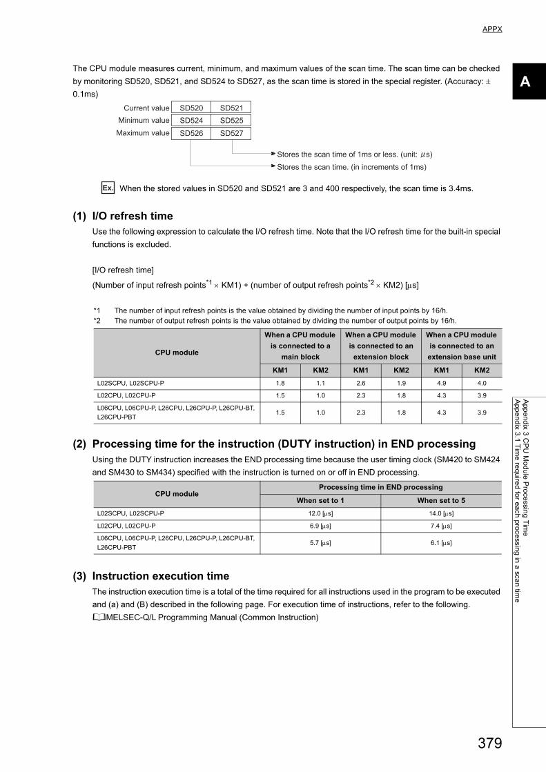
APPX
A
Ap
pe
nd
ix 3 C
PU
Mo
du
le P
roce
ssing
Tim
eA
pp
en
dix 3
.1 T
ime
req
uire
d fo
r ea
ch p
roce
ssing
in a
scan
time
The CPU module measures current, minimum, and maximum values of the scan time. The scan time can be checked
by monitoring SD520, SD521, and SD524 to SD527, as the scan time is stored in the special register. (Accuracy:
0.1ms)
Ex. When the stored values in SD520 and SD521 are 3 and 400 respectively, the scan time is 3.4ms.
(1) I/O refresh timeUse the following expression to calculate the I/O refresh time. Note that the I/O refresh time for the built-in special
functions is excluded.
[I/O refresh time]
(Number of input refresh points*1 KM1) + (number of output refresh points*2 KM2) [s]
*1 The number of input refresh points is the value obtained by dividing the number of input points by 16/h.*2 The number of output refresh points is the value obtained by dividing the number of output points by 16/h.
(2) Processing time for the instruction (DUTY instruction) in END processingUsing the DUTY instruction increases the END processing time because the user timing clock (SM420 to SM424
and SM430 to SM434) specified with the instruction is turned on or off in END processing.
(3) Instruction execution timeThe instruction execution time is a total of the time required for all instructions used in the program to be executed
and (a) and (B) described in the following page. For execution time of instructions, refer to the following.
MELSEC-Q/L Programming Manual (Common Instruction)
CPU module
When a CPU module
is connected to a
main block
When a CPU module
is connected to an
extension block
When a CPU module
is connected to an
extension base unit
KM1 KM2 KM1 KM2 KM1 KM2
L02SCPU, L02SCPU-P 1.8 1.1 2.6 1.9 4.9 4.0
L02CPU, L02CPU-P 1.5 1.0 2.3 1.8 4.3 3.9
L06CPU, L06CPU-P, L26CPU, L26CPU-P, L26CPU-BT,
L26CPU-PBT1.5 1.0 2.3 1.8 4.3 3.9
CPU moduleProcessing time in END processing
When set to 1 When set to 5
L02SCPU, L02SCPU-P 12.0 [s] 14.0 [s]
L02CPU, L02CPU-P 6.9 [s] 7.4 [s]
L06CPU, L06CPU-P, L26CPU, L26CPU-P, L26CPU-BT,
L26CPU-PBT5.7 [s] 6.1 [s]
Stores the scan time of 1ms or less. (unit: s)
Stores the scan time. (in increments of 1ms)
SD520
SD524
SD526
Current value
Minimum value
Maximum value
SD521
SD525
SD527
379

(a) Overhead time at execution of interrupt and fixed scan execution type programs
When using an interrupt or fixed scan execution type program, add the overhead time given in the following
table. Two kinds of overhead time (pre-start and program-end) need to be added to interrupt programs.
(b) Overhead time when local devices in the interrupt program are enabled
Add the overhead time given in the following table when use of local devices is enabled in the interrupt program
by turning on SM777 (Enable/disable local device in interrupt program).
[Pre-start overhead time for interrupt programs]
(N1 KM1) + ((N2 + (N3 16)) KM2) + KM3 [s]
[Overhead time after interrupt program activation]
(N1 KM4) + ((N2 + (N3 16)) KM5) + KM6 [s]
• N1: Number of devices that is specified as a local device (The index register is excluded.)
• N2: Number of word device points (The index register is excluded.)
• N3: Number of bit device points
CPU module
Pre-start overhead time for interrupt programs
Interrupt from the built-in I/O
(I0 to I15)
Fixed scan interrupt (I28 to
I31)
Interrupt from the intelligent
function module (I50 to I127)
Without high-
speed start
With high-
speed start
Without high-
speed start
With high-
speed start
Without high-
speed start
With high-
speed start
L02SCPU,
L02SCPU-P65.0 [s] 31.0 [s] 55.0 [s] 35.0 [s] 76.0 [s] 55.0 [s]
L02CPU, L02CPU-P 57.0 [s] 19.0 [s] 51.0 [s] 17.0 [s] 66.0 [s] 31.0 [s]
L06CPU, L06CPU-P,
L26CPU, L26CPU-P,
L26CPU-BT,
L26CPU-PBT
54.0 [s] 18.0 [s] 46.0 [s] 16.0 [s] 61.0 [s] 26.0 [s]
CPU moduleProgram-end overhead time for interrupt programs
Without high-speed start With high-speed start
L02SCPU, L02SCPU-P 28.0 [s] 15.0 [s]
L02CPU, L02CPU-P 28.0 [s] 9.0 [s]
L06CPU, L06CPU-P, L26CPU, L26CPU-P, L26CPU-BT,
L26CPU-PBT26.0 [s] 8.5 [s]
CPU moduleOverhead time for fixed scan execution type programs
Without high-speed start With high-speed start
L02SCPU, L02SCPU-P 92.0 [s] 60.0 [s]
L02CPU, L02CPU-P 77.0 [s] 25.0 [s]
L06CPU, L06CPU-P, L26CPU, L26CPU-P, L26CPU-BT,
L26CPU-PBT72.0 [s] 23.0 [s]
CPU module KM1 KM2 KM3 KM4 KM5 KM6
L02SCPU, L02SCPU-P 13.2 0.22 210.0 8.0 0.23 30.0
L02CPU, L02CPU-P 8.0 0.22 90.0 8.0 0.22 30.0
L06CPU, L06CPU-P, L26CPU, L26CPU-P, L26CPU-BT,
L26CPU-PBT8.0 0.10 80.0 8.0 0.10 20.0
380

APPX
A
Ap
pe
nd
ix 3 C
PU
Mo
du
le P
roce
ssing
Tim
eA
pp
en
dix 3
.1 T
ime
req
uire
d fo
r ea
ch p
roce
ssing
in a
scan
time
(4) Refresh timeRefresh time is the total time required for refresh of each network and auto refresh of the intelligent function
module.
(a) Refresh time of CC-Link IE Field Network
This is the time required for refresh of CC-Link IE Field Network.
MELSEC-L CC-Link IE Field Network Master/Local Module User's Manual
(b) Auto refresh time of CC-Link
This is the time required for auto refresh of CC-Link.
MELSEC-L CC-Link System Master/Local Module User's Manual
(c) Link refresh time of CC-Link IE Field Network Basic
This is the time required for refresh of CC-Link IE Field Network Basic.
[Refresh time of CC-Link IE Field Network Basic]
T = KM1 + KM2 (((RX + RY) 16) + RWw + RWr) + E [s]
E = KM3 + KM4 (((RX + RY) 16) + RWw + RWr) [s]
• T: Link refresh time
• E: Link refresh time when the file register (R, ZR) is used*1
• RX: Number of points of remote input (RX) refreshed by the master station*2
• RY: Number of points of remote output (RY) refreshed by the master station*2
• RWw: Number of points of remote register (RWw) refreshed by the master station*2
• RWr: Number of points of remote register (RWr) refreshed by the master station*2
• KM1 to KM4: Constant
*1 This time is added when the file register (R, ZR) is used.*2 This value is determined according to the number of slave stations to be connected and the number of occupied
stations.
(d) Auto refresh time via intelligent function modules
This is the time required for refreshing data between the buffer memory of an intelligent function module and
devices in the CPU module.
[Auto refresh time via intelligent function modules]
M1 + KM2 (number of refresh points) [s]
CPU module KM1 KM2 KM3 KM4
L02CPU, L02CPU-P 142.0 0.28 10.7 0.32
L06CPU, L06CPU-P, L26CPU, L26CPU-P, L26CPU-BT,
L26CPU-PBT120.0 0.21 8.5 0.23
CPU module
When a CPU module is
connected to a main block
When a CPU module is
connected to an extension
block
KM1 KM2 KM1 KM2
L02SCPU, L02SCPU-P 96.3 6.7 79.7 8.1
L02CPU, L02CPU-P 6.0 5.0 7.0 6.0
L06CPU, L06CPU-P, L26CPU, L26CPU-P, L26CPU-BT,
L26CPU-PBT4.0 5.0 5.0 6.0
381

(5) Function execution time in END processingThis is the time required for updating calendar or clearing error in END processing.
(a) Calendar update processing time
When SM210 (Clock data set request) turned from off to on or when SM213 (Clock data read request) turned
on, the processing time for changing or reading the clock data are required in END processing.
(b) Error clear processing time
Upon the rising edge of SM50 (Error reset), the processing time for clearing the continuation error stored in
SD50 is required
(c) Error clear processing time by error type
The processing time for clearing the continuation error by error time is required.
CPU module
Processing time
When the clock data set request
is issued
When the clock data read
request is issued
L02SCPU, L02SCPU-P 0.053 [ms] 0.017 [ms]
L02CPU, L02CPU-P 0.025 [ms] 0.006 [ms]
L06CPU, L06CPU-P, L26CPU, L26CPU-P, L26CPU-BT,
L26CPU-PBT0.018 [ms] 0.006 [ms]
CPU moduleProcessing time
When the annunciator is cleared When the error is cleared
L02SCPU, L02SCPU-P 0.185 [ms] 0.180 [ms]
L02CPU, L02CPU-P 0.101 [ms] 0.098 [ms]
L06CPU, L06CPU-P, L26CPU, L26CPU-P, L26CPU-BT,
L26CPU-PBT0.075 [ms] 0.072 [ms]
CPU moduleProcessing time
When the annunciator is cleared When the error is cleared
L02SCPU, L02SCPU-P 0.205 [ms] 0.195 [ms]
L02CPU, L02CPU-P 0.117 [ms] 0.111 [ms]
L06CPU, L06CPU-P, L26CPU, L26CPU-P, L26CPU-BT,
L26CPU-PBT0.090 [ms] 0.087 [ms]
382
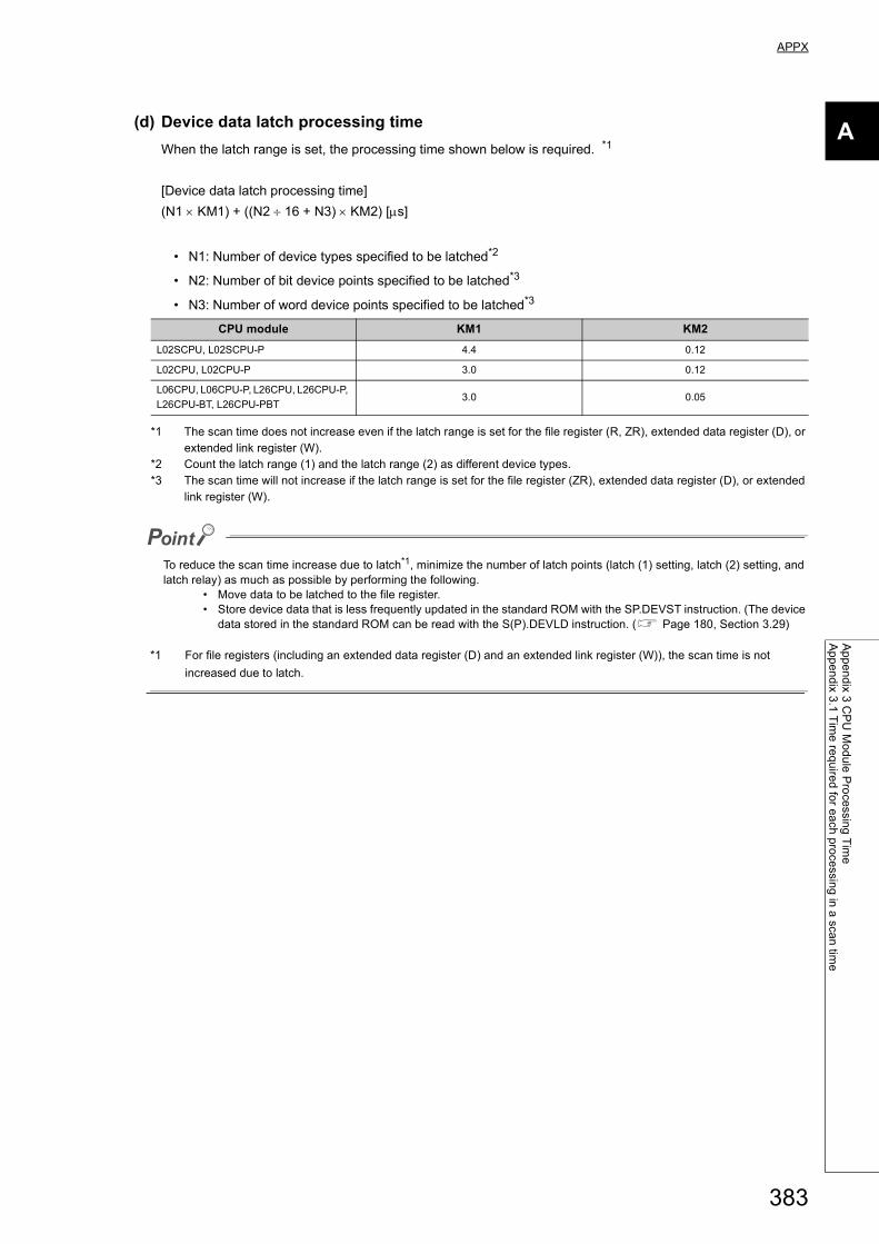
APPX
A
Ap
pe
nd
ix 3 C
PU
Mo
du
le P
roce
ssing
Tim
eA
pp
en
dix 3
.1 T
ime
req
uire
d fo
r ea
ch p
roce
ssing
in a
scan
time
(d) Device data latch processing time
When the latch range is set, the processing time shown below is required. *1
[Device data latch processing time]
(N1 KM1) + ((N2 16 + N3) KM2) [s]
• N1: Number of device types specified to be latched*2
• N2: Number of bit device points specified to be latched*3
• N3: Number of word device points specified to be latched*3
*1 The scan time does not increase even if the latch range is set for the file register (R, ZR), extended data register (D), or extended link register (W).
*2 Count the latch range (1) and the latch range (2) as different device types.*3 The scan time will not increase if the latch range is set for the file register (ZR), extended data register (D), or extended
link register (W).
To reduce the scan time increase due to latch*1, minimize the number of latch points (latch (1) setting, latch (2) setting, and latch relay) as much as possible by performing the following.
• Move data to be latched to the file register.• Store device data that is less frequently updated in the standard ROM with the SP.DEVST instruction. (The device
data stored in the standard ROM can be read with the S(P).DEVLD instruction. ( Page 180, Section 3.29)
CPU module KM1 KM2
L02SCPU, L02SCPU-P 4.4 0.12
L02CPU, L02CPU-P 3.0 0.12
L06CPU, L06CPU-P, L26CPU, L26CPU-P,
L26CPU-BT, L26CPU-PBT3.0 0.05
*1 For file registers (including an extended data register (D) and an extended link register (W)), the scan time is not
increased due to latch.
383

(6) Service processing timeThe following shows the service processing time required for each communication function when the number of
processing is set to one.
(7) Common processing timeThe CPU module performs common processing by the system. The common processing time shown below is
required.
*1 Processing time when the setting of the built-in CC-Link is disabled
CPU
module
Processing time
Program read (when a
10K-step program file
is read)
Online change in the
ladder mode (when
adding 100 steps to the
start of an 8K-step
program)
Online change in the
ladder mode (when
adding 100 steps to the
start of a 20K-step
program)
Online change (file)
(when a 10K-step
program file is read)
Device data Monitor
(Data register: 32
points)
L02SCPU,
L02SCPU-P3.70 [ms] 2.45 [ms] 7.00 [ms] 2.65 [ms]
L02CPU,
L02CPU-P0.95 [ms] 1.20 [ms] 4.40 [ms] 0.50 [ms]
L06CPU,
L06CPU-P,
L26CPU,
L26CPU-P,
L26CPU-BT,
L26CPU-PBT
0.95 [ms] 1.00 [ms] 3.70 [ms] 0.40 [ms]
CPU module Processing time
L02SCPU, L02SCPU-P 0.28 [ms]
L02CPU, L02CPU-P 0.22 [ms]
L06CPU, L06CPU-P, L26CPU, L26CPU-P, L26CPU-BT, L26CPU-PBT 0.18 [ms]*1
384

APPX
A
Ap
pe
nd
ix 3 C
PU
Mo
du
le P
roce
ssing
Tim
eA
pp
en
dix 3
.2 F
acto
rs tha
t incre
ase
the
scan
time
Appendix 3.2 Factors that increase the scan time
When any of the function or operation described below is executed, the scan time is increased by the amount of its
processing time.
(1) Batch transfer to the program memoryUse the following expression to calculate the increased scan time when data are batch transferred to the program
memory.
[Time required for batch-transferring data to the program memory]
Scan time KM1 + KM2 [s]
(2) Use of local devicesUse the following expression to calculate the increased scan time when local devices are used.
[Increase in the scan time]
((N1 KM1) + ((N2 + N3 16)) KM2) + (N4 KM3) + KM4) n + KM5 [s]
• N1: Number of devices that is specified as a local device
• N2: Number of word device points
• N3: Number of bit device points
• N4: Number of index register points that were specified as a local device
Use the following expression to calculate the increase in scan time when local devices are used in a subroutine
program (only when the subroutine program is called from another file).
[Increase in the scan time]
(N1 KM1) + ((N2 + (N3 16)) KM2) + (N4 KM3) + KM4 [s]
• N1: Number of devices that is specified as a local device
• N2: Number of word device points
• N3: Number of bit device points
• N4: Number of index register points that were specified as a local device
CPU module KM1 KM2
L02SCPU, L02SCPU-P 120.0 1.2
L02CPU, L02CPU-P 170.0 1.0
L06CPU, L06CPU-P 260.0 4.7
L26CPU, L26CPU-P, L26CPU-BT, L26CPU-PBT 1100.0 15.0
CPU module KM1 KM2 KM3 KM4 KM5
L02SCPU, L02SCPU-P 16.0 0.23 1.49 98.3 92.0
L02CPU, L02CPU-P 8.0 0.22 0.65 58.0 14.2
L06CPU, L06CPU-P 8.0 0.10 0.47 35.5 12.7
L26CPU, L26CPU-P, L26CPU-BT, L26CPU-PBT 8.0 0.10 0.68 35.5 17.3
CPU module KM1 KM2 KM3 KM4
L02SCPU, L02SCPU-P 20.3 0.76 4.47 257
L02CPU, L02CPU-P 16.0 0.44 1.30 80.0
L06CPU, L06CPU-P 16.0 0.20 0.94 100.0
L26CPU, L26CPU-P, L26CPU-BT, L26CPU-PBT 16.0 0.20 1.36 100.0
385

(3) Execution of multiple programsUse the following formula to calculate the increase in scan time when executing multiple programs.
[Increase in the scan time]
Number of program files to be executed KM1 [ms]
(4) Removal and insertion of an SD memory cardThe following shows the increase in scan time when an SD memory card is inserted or removed.
(5) Scan time measurementUse the following expression to calculate the increase in scan time when the scan time is set to be measured.
[Increase in the scan time]
KM1 + number of branch instructions*1 KM2 [s]
*1 The number of branch instructions is a total of the following pointer branch instructions and structure creation instructions, which are executed between a start point and an end point of the scan time measurement. Pointer branch instructions: CJ, SCJ, JMP, GOEND Structure creation instruction: CALL(P), FCALL(P), ECALL(P), EFCALL(P), XCALL(P), BREAK, NEXT, RET
(6) A series CPU module compatibility settingThe following shows the increase in scan time when an A series CPU module compatibility setting is enabled.
CPU module KM1
L02SCPU, L02SCPU-P 0.053
L02CPU, L02CPU-P 0.024
L06CPU, L06CPU-P, L26CPU, L26CPU-P, L26CPU-BT, L26CPU-PBT 0.02
CPU module
Increase in scan time
When an SD memory card is
inserted
When an SD memory card is
removed
L02CPU, L02CPU-P 0.89 [ms] 0.49 [ms]
L06CPU, L06CPU-P, L26CPU, L26CPU-P, L26CPU-BT,
L26CPU-PBT0.82 [ms] 0.42 [ms]
CPU module KM1 KM2
L02SCPU, L02SCPU-P 179.5 5.8
L02CPU, L02CPU-P 40.0 1.7
L06CPU, L06CPU-P, L26CPU, L26CPU-P, L26CPU-BT,
L26CPU-PBT40.0 1.5
CPU module Increase in scan time
L02SCPU, L02SCPU-P 95 [s]
L02CPU, L02CPU-P 40 [s]
L06CPU, L06CPU-P, L26CPU, L26CPU-P, L26CPU-BT, L26CPU-PBT 34 [s]
386

APPX
A
Ap
pe
nd
ix 3 C
PU
Mo
du
le P
roce
ssing
Tim
eA
pp
en
dix 3
.2 F
acto
rs tha
t incre
ase
the
scan
time
(7) Time taken to collect module errorsUse the following formula to calculate the increase in scan time when the module error collection function is used.
[Increase in the scan time]
KM1 + (N1 KM2) + (N2 KM3) [s]
• N1: Number of errors collected per scan by the built-in CC-Link or external modules
• N2: Number of errors collected by the built-in I/O
(8) Data logging functionFor the increase in scan time when using the data logging function, refer to the following.
QnUDVCPU/LCPU User's Manual (Data Logging Function)
(9) Realtime monitor functionUse the following formula to calculate the increase in scan time on the realtime monitor function.
[Increase in the scan time]
KM1 + ( KM2 N1 ) + ( KM3 N2 ) [s]
• N1: Number of word devices
• N2: Number of bit devices
• KM1: Constant (common processing time)
• KM2: Constant (word device processing time)
• KM3: Constant (bit device processing time)
Internal user device (X, Y, M, L, B, F, SB, V, T, ST, C, D, W, SW, FX, FY, FD, SM, SD, BL\S)
File register (R, ZR)
CPU module
When a CPU module is connected to
a main block
When a CPU module is connected to
an extension block
KM1 KM2 KM3 KM1 KM2 KM3
L02SCPU, L02SCPU-P 145 120 80 190 140 70
L02CPU, L02CPU-P 28 80 60 28 105 50
L06CPU, L06CPU-P, L26CPU, L26CPU-P,
L26CPU-BT, L26CPU-PBT21 70 50 21 100 40
CPU module KM1 KM2 KM3
L02CPU, L02CPU-P 79.00 0.68 0.95
L06CPU, L06CPU-P 74.00 0.60 0.87
L26CPU, L26CPU-P, L26CPU-BT, L26CPU-PBT 64.00 0.56 0.75
CPU module KM1 KM2 KM3
L02CPU, L02CPU-P 79.00 0.78 1.11
L06CPU, L06CPU-P 74.00 0.70 1.03
L26CPU, L26CPU-P, L26CPU-BT, L26CPU-PBT 64.00 0.66 0.91
387

Module access device (U\G),
Link direct device(J\W, J\X, J\SW, J\Y, J\SB)
Appendix 3.3 Realtime monitor function processing time
This is the minimum interval for monitoring data without any loss under the following conditions during the execution of
the realtime monitor function.
• Scan time = 1.5ms (up to 3ms)*1
• Timing = Select "Step No. Specification" as timing condition and set conditions.*2
• Buffer capacity = 32K bytes
• Fixed scan interrupt timing = Start step number of the program set as a condition under "Step No.
Specification"
*1 The average scan time shall be 1.0ms when the realtime monitor function is not executed.*2 Program name: Any, Step No.: Start step of the program, Execution condition: "Always"
CPU module KM1 KM2 KM3
L02CPU, L02CPU-P 128.10 14.50 15.06
L06CPU, L06CPU-P 125.12 14.20 15.00
L26CPU, L26CPU-P, L26CPU-BT, L26CPU-PBT 112.00 12.00 13.50
Cable type Number of word device points Monitor interval
USB1 or 8 0.5ms
16 1.0ms
Ethernet1 0.5ms
8 or 16 1.0ms
RS-232
1 1.50ms
8 3.50ms
16 5.50ms
388

APPX
A
Ap
pe
nd
ix 4 D
ata
Use
d in
the
CP
U M
od
ule
Appendix 4 Data Used in the CPU Module
In the CPU module, data such as numeric values and alphabets are represented as a series of bits, "0" and "1". This
notation is called BIN (binary).
In addition, DEC (decimal), HEX (hexadecimal), BCD (binary-coded decimal), and floating-point data are available.
(1) BIN (binary code)BIN is a data notation where a value is represented as a series of bits "0" and "1". Each place digit is shifted to the
higher digit when the value exceeds 1.
The value ranged from -32768 to 32767 can be stored in the CPU module.
(2) DEC (decimal)DEC represents binary data of the CPU module in decimal notation. ( Page 342, Section 6.2)
(3) HEX (hexadecimal)HEX represents binary data of the CPU module in hexadecimal notation. ( Page 343, Section 6.3)
In hexadecimal notation, four bits are handled as one digit. Because the place value in a digit is from 0 to 15 in
decimal notation, a value larger than nine is represented by A, B, C, D, E, or F. When the value is larger than F,
the digit is shifted to the higher digit.
This notation is useful when using 16-bit devices such as the data register and link register.
(4) BCD (binary-coded decimal)BCD is a data notation that represents a value in the ones place of a decimal number in a binary number. As with
hexadecimal notation, data are represented in four bits but the alphabets A to F are not used. This notation is
useful when handling data from external devices, such as digital switches.
(5) Floating-point dataIn floating point data, real number data are handled as a numeric value with the decimal point. The single-
precision floating-point data and double-precision floating-point data are available. ( Page 343, Section 6.4)
b15
8192
Bit name
Bit weight
Most significant bit (for determination of positive/negative value)
A value is negative when the most significant bit is "1".
16384 4096 2048 1024 512 256 128 64 32 16 8 4 2 1-32768
215 214 213 212 211 210 29 28 27 26 25 24 23 22 21 20
b14 b13 b12 b11 b10 b9 b8 b7 b6 b5 b4 b3 b2 b1 b0
Decimal value
389

(6) Numeric representation listThe following table shows the numeric representation of BIN (binary), DEC (decimal), HEX (hexadecimal), and
BCD (binary-coded decimal).
BIN (binary) DEC (decimal) HEX (hexadecimal) BCD (binary-coded decimal)
0 0 0 0
1 1 1 1
10 2 2 10
11 3 3 11
4 4
5 5
6 6
7 7
8 8
1001 9 9 1001
1010 10 A 1 0000
1011 11 B 1 0001
1100 12 C 1 0010
1101 13 D 1 0011
1110 14 E 1 0100
1111 15 F 1 0101
1 0000 16 10 1 0110
1 0001 17 11 1 0111
10 1111 47 2F 100 0111
0111 1111 1111 1110 32766 7FFE
0111 1111 1111 1111 32767 7FFF
1000 0000 0000 0000 -32768 8000 1000 0000 0000 0000
1000 0000 0000 0001 -32767 8001 1000 0000 0000 0001
1111 1111 1111 1110 -2 FFFE
1111 1111 1111 1111 -1 FFFF
390

APPX
A
Ap
pe
nd
ix 5 C
ha
racte
r Co
de
s Ava
ilab
le in
the
Disp
lay U
nit
Appendix 5 Character Codes Available in the Display Unit
The following chart shows character codes available in the display unit.
*1 "0081H to 009FH" and "00E0H to 00FCH" are recognized as upper bytes of the Shift-JIS code.
391

The parts in the tables on the following pages are out of the Shift-JIS code range. The Shift-JIS code range is
"81H to 9FH" and "E0H to FCH" for upper bytes, and "40H to 7EH" and "80H to FCH" for lower bytes.
392

APPX
A
Ap
pe
nd
ix 5 C
ha
racte
r Co
de
s Ava
ilab
le in
the
Disp
lay U
nit
393

394

APPX
A
Ap
pe
nd
ix 5 C
ha
racte
r Co
de
s Ava
ilab
le in
the
Disp
lay U
nit
395

396

APPX
A
Ap
pe
nd
ix 5 C
ha
racte
r Co
de
s Ava
ilab
le in
the
Disp
lay U
nit
397

398

APPX
A
Ap
pe
nd
ix 5 C
ha
racte
r Co
de
s Ava
ilab
le in
the
Disp
lay U
nit
399

400

APPX
A
Ap
pe
nd
ix 5 C
ha
racte
r Co
de
s Ava
ilab
le in
the
Disp
lay U
nit
401

402

APPX
A
Ap
pe
nd
ix 6 D
iffere
nce
s Be
twe
en
LC
PU
an
d Q
nU
CP
UA
pp
en
dix 6
.1 S
pe
cificatio
ns co
mp
ariso
n
Appendix 6 Differences Between LCPU and QnUCPU
This section describes the specifications comparison between the LCPU and QnCPU and the precautions for using the
existing system.
Appendix 6.1 Specifications comparison
The following table shows a comparison of the specifications between LCPU and QnCPU.
Item DescriptionDifference
LCPU QnUCPU
System
configuration
Basic configuration
• Power supply module
• CPU module
• I/O modules and intelligent function modules
• END cover
• Power supply module
• CPU module
• I/O modules and intelligent function modules
• Base unit
Module installation Modules are connected in order. Modules are mounted on the base unit.
Number of modules
• Module whose serial number (first five digit) is
"13071" or earlier: Up to 10 modules
• Module whose serial number (first five digits) is
"13072" or later: Up to 40 modules (L02SCPU,
L02SCPU-P, L02CPU, and L02CPU-P: Up to 30
modules)
Note that a power supply module, CPU module,
display unit, branch module, extension module, RS-
232 adapter, and END cover are not included.
Up to 64 modules (Q00UJCPU: 16 modules,
Q00U/Q01UCPU: 24 modules, Q02UCPU: 32
modules)
System extension
• Module whose serial number (first five digit) is
"13071" or earlier: Not allowed
• Module whose serial number (first five digit) is
"13072" or later: Allowed
Allowed
Power supply module ERR contact not provided ERR contact provided
Multiple CPU system
configurationNot available Available
Redundant power supply
system configurationNot available Available
Memory card type SD memory card
• SRAM memory card
• Flash memory card
• ATA memory card
• SD memory card (only QnUDVCPU and
QnUDPVCPU)
Built-in functionSerial communication
function
Available
• L02SCPU
• L02SCPU-P
• CPU module where the RS-232 adapter or RS-
422/485 adapter can be mounted (the one whose
serial number (first five digits) is "15102" or later)
Available
• Q00U(J)/Q01UCPU
• Q02UCPU whose serial number (first five digits) is
"10102" or later
• Q03UD/Q04UDH/Q06UDH/Q10UDH/Q13UDH/Q2
0UDH/Q26UDHCPU whose serial number (first
five digits) is "13062" or later only
403

Appendix 6.2 Precautions for utilizing programs
This section describes precautions for applying a QnCPU program to the LCPU.
(1) I/O assignmentSince the LCPU is equipped with built-in functions, the start I/O number assigned by default is different from that
of the QnCPU. Therefore, to use the programs of the QnCPU, I/O assignments must be changed even if the
configuration of the module has been the same. Change the start I/O number of the connected module in the I/O
Assignment tab of the PLC Parameter dialog box according to the program. ( Page 364, Appendix 1.2 (9))
(2) InstructionsSome instructions among those applicable to the QnCPU cannot be used in the LCPU. The following table shows
the instructions not applicable to the LCPU.
*1 Only the Q00UCPU, Q01UCPU, and Q02UCPU support these instructions.*2 The Universal model QCPUs (except the Q00UJCPU, Q00UCPU, Q01UCPU, and Q02UCPU) support these
instructions.
Classification Instruction
Application instruction
File register switching instruction File set QDRSET(P)
Other instructions
Reading routing information S(P).RTREAD
Registering routing information S(P).RTWRITE
File register high-speed block transfer RBMOV(P)
Multiple CPU dedicated
instruction
CPU module shared memory
access instruction
Write to host CPU shared memory
S(P).TO
TO(P)
DTO(P)
Reading from the CPU shared memory of another CPUFROM(P)
DFRO(P)
Motion CPU dedicated instruction *1
Motion SFC program startup request S(P).SFCS
Servo program startup request S(P).SVST
Axis speed change during positioning and JOG operation S(P).CHGV
Torque control value change during operation and suspension
in real modeS(P).CHGT
Current value change of halted axis/synchronized
encoder/cam axisS(P).CHGA
Write device data to motion controller S(P).DDWR
Read device data from motion controller S(P).DDRD
Multiple CPU high speed bus
compatible Motion CPU dedicated
instruction*2
Motion SFC program startup request D(P).SFCS
Servo program startup request D(P).SVST
Axis speed change during positioning and JOG operation D(P).CHGV
Torque control value change during operation and suspension
in real modeD(P).CHGT
Current value change of halted axis/synchronized
encoder/cam axisD(P).CHGA
Multiple CPU high speed bus
compatible NC dedicated
instruction*2
ATC dedicated instruction D(P).ATC
Rotation control instruction D(P).ROT
Another CPU access instruction*1 Other CPU interrupt program startup S(P).GINT
Multiple CPU high speed bus
compatible other CPU access
instruction*2
Writing devices to another CPU D(P).DDWR
Reading devices to another CPU D(P).DDRD
Other CPU (motion controller) interrupt program startup D(P).GINT
404

405
APPX
A
Ap
pe
nd
ix 7 P
reca
utio
ns fo
r Usin
g G
X W
orks2
an
d D
iffere
nce
s with
GX
De
velo
pe
r
Appendix 7 Precautions for Using GX Works2 and Differences with GX Developer
For the precautions for using GX Works2 and differences with GX Developer, refer to the following.
GX Works2 Version 1 Operating Manual (Common)

406
Appendix 8 Device Point Assignment Sheet
*1 Up to 32K points can be set for each device. (60K for the internal relay and link relay.)
*2 Enter the values multiplied (or divided) by the number shown in the Size (words) column.
Device name SymbolNumeric
notation
Number of device points*1 Restriction check
Points Range Size (words)*2 Points (bits)*1
Input relay X 16 8K (8192) X0000 to X1FFF 16 512 1 8192
Output relay Y 16 8K (8192) Y0000 to Y1FFF 16 512 1 8192
Internal relay M 10 K ( ) M0 to 16 1
Latch relay L 10 K ( ) L0 to 16 1
Link relay B 16 K ( ) B0000 to 16 1
Annunciator F 10 K ( ) F0 to 16 1
Link special relay SB 16 K ( ) SB0000 to 16 1
Edge relay V 10 K ( ) V0 to 16 1
Step relay S 10 8K (8192) S0 to S8191 16 512 1
Timer T 10 K ( ) T0 to 2
Retentive timer ST 10 K ( ) ST0 to 2
Counter C 10 K ( ) C0 to 2
Data register D 10 K ( ) D0 to 1
Link register W 16 K ( ) W0000 to 1
Link special register SW 16 K ( ) SW0000 to 1
Total (29696 or less)
18
16
18
16
18
16

I
4
4
7
8
INDEX
A
Acknowledge XY Assignment. . . . . . . . . . . . . . . . 366Allowable momentary power failure time . . . . . . . . . 50Annunciator (F). . . . . . . . . . . . . . . . . . . . . . . . . . 295Automatic data transfer to the program memory . . . 157
B
Backlight . . . . . . . . . . . . . . . . . . . . . . . . . . . . . . 238Backup data restoration . . . . . . . . . . . . . . . . . . . . 192Backup to SD memory card . . . . . . . . . . . . . . . . . 184Batch-disabling executional conditioned device test settings . . . . . . . . . . . . . . . . . . . . . . . . . . . . 140Battery. . . . . . . . . . . . . . . . . . . . . . . . . . . . . . . . . 18Battery life-prolonging function . . . . . . . . . . . . . . . 198BCD (binary-coded decimal) . . . . . . . . . . . . . . . . 389BIN (binary code) . . . . . . . . . . . . . . . . . . . . . . . . 389Block switching method (R) . . . . . . . . . . . . . . . . . 326Boot file setting . . . . . . . . . . . . . . . . . . . . . . . . . . 359Boot operation . . . . . . . . . . . . . . . . . . . . . . . . . . . 74Buffer memory monitor . . . . . . . . . . . . . . . . . . . . 268Buffer memory monitor/test . . . . . . . . . . . . . . . . . 265Buffer memory test . . . . . . . . . . . . . . . . . . . . . . . 269Built-in Ethernet port setting . . . . . . . . . . . . . . . . . 367Built-in high-speed counter function monitor. . . . . . 256Built-in I/O function error clear . . . . . . . . . . . . . . . 258Built-in I/O function monitor . . . . . . . . . . . . . . . . . 255Built-in I/O Function Setting . . . . . . . . . . . . . . . . . 369Built-in positioning function monitor . . . . . . . . . . . . 256Built-in serial setting . . . . . . . . . . . . . . . . . . . . . . 370
C
Changing a remote password. . . . . . . . . . . . . . . . 111Changing clock data . . . . . . . . . . . . . . . . . . . . . . 196Changing the program execution type . . . . . . . . . . . 72Character codes available in the display unit . . . . . 391Character string (" ") . . . . . . . . . . . . . . . . . . . . . . 343Checking the executional conditioned device test . . 139Clearing the file register . . . . . . . . . . . . . . . . . . . . 329Clock data read . . . . . . . . . . . . . . . . . . . . . . . . . 197Clock function. . . . . . . . . . . . . . . . . . . . . . . . . . . 196Clock setting. . . . . . . . . . . . . . . . . . . . . . . . . . . . 263Common pointer . . . . . . . . . . . . . . . . . . . . . . . . . 338Common processing time . . . . . . . . . . . . . . . . . . 384Compilation . . . . . . . . . . . . . . . . . . . . . . . . . . . . . 25Constant scan . . . . . . . . . . . . . . . . . . . . . . . . . . . 85Constants. . . . . . . . . . . . . . . . . . . . . . . . . . . . . . 342Contrast adjustment . . . . . . . . . . . . . . . . . . . . . . 284Converting a program . . . . . . . . . . . . . . . . . . . . . . 25Counter (C) . . . . . . . . . . . . . . . . . . . . . . . . . . . . 308CPU module change function with SD memory card. . . . . . . . . . . . . . . . . . . . . . . . . . . . . . . . . . 182CPU monitor/test . . . . . . . . . . . . . . . . . . . . . . . . 241CPU settings . . . . . . . . . . . . . . . . . . . . . . . . . . . 263Creating a program . . . . . . . . . . . . . . . . . . . . . . . . 23Current value changing . . . . . . . . . . . . . . . . . . . . . 29
D
Data acquisition timing setting . . . . . . . . . . . . . . . 146Data logging file . . . . . . . . . . . . . . . . . . . . . . . . . . 33Data logging setting file . . . . . . . . . . . . . . . . . . . . . 33Data register (D). . . . . . . . . . . . . . . . . . . . . . . . . 311Debug from multiple programming tools . . . . . . . . 158DEC (decimal) . . . . . . . . . . . . . . . . . . . . . . . . . . 389Decimal constant (K). . . . . . . . . . . . . . . . . . . . . . 342Deleting a file register file . . . . . . . . . . . . . . . . . . 329Deleting a remote password . . . . . . . . . . . . . . . . 111Device clear . . . . . . . . . . . . . . . . . . . . . . . . . . . . 249Device comment. . . . . . . . . . . . . . . . . . . . . . . . . . 33Device memory clear . . . . . . . . . . . . . . . . . . . . . 249Device monitor . . . . . . . . . . . . . . . . . . . . . . . . . . 245Device monitor/test . . . . . . . . . . . . . . . . . . . . . . . 241Device point assignment sheet. . . . . . . . . . . 292,406Device setting . . . . . . . . . . . . . . . . . . . . . . . . . . 362Device test. . . . . . . . . . . . . . . . . . . . . . . . . 130,248Differences between LCPU and QnUCPU . . . . . . . 403Direct processing . . . . . . . . . . . . . . . . . . . . . . . . . 54Disable the pop-up display. . . . . . . . . . . . . . . . . . 273Disabling the executional conditioned device test . . 139Display unit functions . . . . . . . . . . . . . . . . . . . . . 236Drive heading. . . . . . . . . . . . . . . . . . . . . . . . . . . . 33
E
Edge relay (V) . . . . . . . . . . . . . . . . . . . . . . . . . . 298Enable pop-up display. . . . . . . . . . . . . . . . . . . . . 286END cover . . . . . . . . . . . . . . . . . . . . . . . . . . . . . . 18END processing . . . . . . . . . . . . . . . . . . . . . . . . . . 47Error clear . . . . . . . . . . . . . . . . . . . . . . . . . . . . . 166Error display/clear. . . . . . . . . . . . . . . . . . . . . . . . 259Error history . . . . . . . . . . . . . . . . . . . . . . . . . . . . 161Error time output mode setting . . . . . . . . . . . . . . . 103Executing a program. . . . . . . . . . . . . . . . . . . . . . . 28Executing a sampling trace . . . . . . . . . . . . . . . . . 147Executing multiple programs . . . . . . . . . . . . . . . . . 61Executional conditioned device test . . . . . . . . . . . 135Extended data register (D). . . . . . . . . . . . . . . . . . 330Extended link register (W) . . . . . . . . . . . . . . . . . . 330Extension. . . . . . . . . . . . . . . . . . . . . . . . . . . . . . . 33External input/output forced on/off . . . . . . . . . . . . 131
F
Factors that increase the scan time . . . . . . . . . . . 385File name. . . . . . . . . . . . . . . . . . . . . . . . . . . . . . . 33File register (R, ZR) . . . . . . . . . . . . . . . . . . . . . . 326File register clear . . . . . . . . . . . . . . . . . . . . . . . . 249Files . . . . . . . . . . . . . . . . . . . . . . . . . . . . . . . . . . 35Fixed scan execution type program . . . . . . . . . . . . 69Floating-point data . . . . . . . . . . . . . . . . . . . . . . . 389Forced on/off . . . . . . . . . . . . . . . . . . . . . . . . . . . 251Format . . . . . . . . . . . . . . . . . . . . . . . . . . . . . . . . 26Format PLC memory. . . . . . . . . . . . . . . . . . . . . . . 26Formatting a memory . . . . . . . . . . . . . . . . . . . . . . 26Function devices (FX, FY, FD) . . . . . . . . . . . . . . . 314Function execution time in END processing. . . . . . 382
407

Function input (FX). . . . . . . . . . . . . . . . . . . . . . . 314Function output (FY). . . . . . . . . . . . . . . . . . . . . . 314Function register (FD). . . . . . . . . . . . . . . . . . . . . 315
G
Global device. . . . . . . . . . . . . . . . . . . . . . . . . . . 344
H
HEX (hexadecimal) . . . . . . . . . . . . . . . . . . . . . . 389Hexadecimal constant (H) . . . . . . . . . . . . . . . . . . 342High-speed timer . . . . . . . . . . . . . . . . . . . . . . . . 300
I
I/O assignment setting . . . . . . . . . . . . . . . . . . . . 364I/O No. specification device (U) . . . . . . . . . . . . . . 340I/O number assignment . . . . . . . . . . . . . . . . . . 42,43I/O numbers . . . . . . . . . . . . . . . . . . . . . . . . . . . . 23I/O refresh time . . . . . . . . . . . . . . . . . . . . . . . . . 379Index register (Z) . . . . . . . . . . . . . . . . . . . . . . . . 322Initial device value . . . . . . . . . . . . . . . . . . . . . . . . 91Initial execution monitoring time. . . . . . . . . . . . . . . 64Initial execution type program . . . . . . . . . . . . . . . . 63Initial processing . . . . . . . . . . . . . . . . . . . . . . . . . 45Initial scan time . . . . . . . . . . . . . . . . . . . . . . . . . . 64Initial setting change. . . . . . . . . . . . . . . . . . . . . . 270Input (X) . . . . . . . . . . . . . . . . . . . . . . . . . . . . . . 293Input response time setting . . . . . . . . . . . . . . . . . 102Instruction execution time . . . . . . . . . . . . . . . . . . 379Instructions do not operate normally during online change . . . . . . . . . . . . . . . . . . . . . . . . . . 153Intelligent function module device . . . . . . . . . . . . 320Intelligent function module interrupt . . . . . . . . . . . 339Intelligent function module parameters . . . . . . . . 33,77Internal relay (M) . . . . . . . . . . . . . . . . . . . . . . . . 294Internal system devices . . . . . . . . . . . . . . . . . . . 314Internal user devices . . . . . . . . . . . . . . . . . . . . . 290Interrupt by an internal timer . . . . . . . . . . . . . . . . 339Interrupt by built-in I/O . . . . . . . . . . . . . . . . . . . . 339Interrupt pointer (I) . . . . . . . . . . . . . . . . . . . . . . . 339Interrupt program . . . . . . . . . . . . . . . . . . . . . . . . . 56Interrupt program list monitor. . . . . . . . . . . . . . . . 122
L
Ladder . . . . . . . . . . . . . . . . . . . . . . . . . . . . . . . . 76Language setting . . . . . . . . . . . . . . . . . . . . . . . . 283Latch data backup . . . . . . . . . . . . . . . . . . . . . . . 176Latch data backup to standard ROM . . . . . . . . . . 175Latch function . . . . . . . . . . . . . . . . . . . . . . . . . . . 88Latch range setting. . . . . . . . . . . . . . . . . . . . . . . . 88Latch relay (L) . . . . . . . . . . . . . . . . . . . . . . . . . . 294LED control function . . . . . . . . . . . . . . . . . . . . . . 169LED indication priority. . . . . . . . . . . . . . . . . . . . . 170Level navigation. . . . . . . . . . . . . . . . . . . . . . . . . 239Lighting period setting . . . . . . . . . . . . . . . . . . . . 285Link register (W) . . . . . . . . . . . . . . . . . . . . . . . . 312Link relay (B) . . . . . . . . . . . . . . . . . . . . . . . . . . . 294Link special register (SW) . . . . . . . . . . . . . . . . . . 313Link special relay (SB) . . . . . . . . . . . . . . . . . . . . 298Local device . . . . . . . . . . . . . . . . . . . . . . . . . . . 345
Local pointer . . . . . . . . . . . . . . . . . . . . . . . . . . . 337Low-speed timer . . . . . . . . . . . . . . . . . . . . . . . . 300
M
Macro instruction argument device (VD). . . . . . . . 341Main routine program. . . . . . . . . . . . . . . . . . . . . . 46Memories . . . . . . . . . . . . . . . . . . . . . . . . . . . . . . 31Menu definition file. . . . . . . . . . . . . . . . . . . . . . . 272Methods for turning off the LEDs . . . . . . . . . . . . . 169Module access devices . . . . . . . . . . . . . . . . . . . 320Module error collection function. . . . . . . . . . . . . . 171Module errors . . . . . . . . . . . . . . . . . . . . . . . . . . 171Module model name read . . . . . . . . . . . . . . . . . . 181Module monitor/test . . . . . . . . . . . . . . . . . . . . . . 265Module settings . . . . . . . . . . . . . . . . . . . . . . . . . 270Monitor . . . . . . . . . . . . . . . . . . . . . . . . . . . . . . . 158Monitoring local devices . . . . . . . . . . . . . . . . . . . 128Multiple timers. . . . . . . . . . . . . . . . . . . . . . . . . . 306
N
Nesting (N) . . . . . . . . . . . . . . . . . . . . . . . . . . . . 335Network parameter . . . . . . . . . . . . . . . . . . . . . . 374
O
Online change (files) . . . . . . . . . . . . . . . . . . . . . 152Online change (ladder mode) . . . . . . . . . . . . . . . 151Online change based on relative step No. . . . . . . 160Online change from multiple programming tools . . 160Options. . . . . . . . . . . . . . . . . . . . . . . . . . . . . . . 283Other devices . . . . . . . . . . . . . . . . . . . . . . . . . . 340Output (Y). . . . . . . . . . . . . . . . . . . . . . . . . . . . . 293Output mode at operating status change (STOP to RUN) . . . . . . . . . . . . . . . . . . . . . . . . . 101Overflow. . . . . . . . . . . . . . . . . . . . . . . . . . . . . . 343
P
Parameter. . . . . . . . . . . . . . . . . . . . . . . . . . . . . . 33Parameter numbers . . . . . . . . . . . . . . . . . . . . . . 350Parameter setting . . . . . . . . . . . . . . . . . . . . . . . 350Parameter-valid drive . . . . . . . . . . . . . . . . . . . . . . 34PAUSE status . . . . . . . . . . . . . . . . . . . . . . . . . . . 48PLC file setting . . . . . . . . . . . . . . . . . . . . . . . . . 356PLC name setting . . . . . . . . . . . . . . . . . . . . . . . 353PLC operation mode at H/W error setting . . . . . . . 104PLC parameter . . . . . . . . . . . . . . . . . . . . . . . . . 353PLC RAS setting . . . . . . . . . . . . . . . . . . . . . . . . 357PLC system setting . . . . . . . . . . . . . . . . . . . . . . 354PLC user data . . . . . . . . . . . . . . . . . . . . . . . . . . . 33Pointer (P) . . . . . . . . . . . . . . . . . . . . . . . . . . . . 336Pop up . . . . . . . . . . . . . . . . . . . . . . . . . . . . . . . 273Pop-up display . . . . . . . . . . . . . . . . . . . . . . . . . 286Predefined protocol function . . . . . . . . . . . . . . . . 215Processing time for the instruction (DUTY instruction) in END processing . . . . . . . . . . . . . . . . . . . . . . . 379Program . . . . . . . . . . . . . . . . . . . . . . . . . . . . . 23,33Program cache memory . . . . . . . . . . . . . . . . . . . . 31Program file . . . . . . . . . . . . . . . . . . . . . . . . . . . . 39Program list monitor. . . . . . . . . . . . . . . . . . . . . . 121Program memory. . . . . . . . . . . . . . . . . . . . . . . . . 31
408

I
4
4
7
8
Program operation . . . . . . . . . . . . . . . . . . . . . . . . 46Program setting . . . . . . . . . . . . . . . . . . . . . . . . . 360Programming language . . . . . . . . . . . . . . . . . . . . . 76Programming tool . . . . . . . . . . . . . . . . . . . . . . . . . 18Project . . . . . . . . . . . . . . . . . . . . . . . . . . . . . . . . . 22
Q
QnUCPU . . . . . . . . . . . . . . . . . . . . . . . . . . . . . . . 18
R
Real number (E) . . . . . . . . . . . . . . . . . . . . . . . . . 343Refresh processing . . . . . . . . . . . . . . . . . . . . . . . . 51Refresh processing of input/output modules or intelligent function modules . . . . . . . . . . . . . . . . . . 46Refresh time. . . . . . . . . . . . . . . . . . . . . . . . . . . . 381Registering executional conditioned device test settings . . . . . . . . . . . . . . . . . . . . . . . . . . . . . . . 136Registering/canceling display unit menu . . . . . . . . 272Remote latch clear . . . . . . . . . . . . . . . . . . . . . . . 117Remote operation . . . . . . . . . . . . . . . . . . . . . . . . 112Remote password . . . . . . . . . . . . . . . . . . . . . . . . 375Remote PAUSE . . . . . . . . . . . . . . . . . . . . . . . . . 114Remote RESET . . . . . . . . . . . . . . . . . . . . . . . . . 116Remote RUN . . . . . . . . . . . . . . . . . . . . . . . . . . . 112Remote STOP . . . . . . . . . . . . . . . . . . . . . . . . . . 112Restoring backup data. . . . . . . . . . . . . . . . . . . . . 179Retentive timer . . . . . . . . . . . . . . . . . . . . . . . . . . 301RUN status. . . . . . . . . . . . . . . . . . . . . . . . . . . . . . 48
S
Sampling trace . . . . . . . . . . . . . . . . . . . . . . . . . . 143Sampling trace file . . . . . . . . . . . . . . . . . . . . . . . 143Saving a project . . . . . . . . . . . . . . . . . . . . . . . . . . 30Saving and restoration of the index register . . . . . . 324Scan execution type program. . . . . . . . . . . . . . . . . 65Scan time measurement . . . . . . . . . . . . . . . . . . . 118Scan time monitor . . . . . . . . . . . . . . . . . . . . . . . . 254Scan time structure . . . . . . . . . . . . . . . . . . . . . . . . 45Scrolling. . . . . . . . . . . . . . . . . . . . . . . . . . . . . . . 239SD memory card. . . . . . . . . . . . . . . . . . . . . . . 18,32Self-diagnostic function . . . . . . . . . . . . . . . . 161,238Serial communication function . . . . . . . . . . . . . . . 227Serial number access method (ZR) . . . . . . . . . . . . 326Service processing setting . . . . . . . . . . . . . . . . . . . 94Service processing time. . . . . . . . . . . . . . . . . . . . 384SFC. . . . . . . . . . . . . . . . . . . . . . . . . . . . . . . . . . . 76SFC block device (BL) . . . . . . . . . . . . . . . . . . . . . 340SFC setting . . . . . . . . . . . . . . . . . . . . . . . . . . . . 361Simultaneous monitoring from multiple programming tools . . . . . . . . . . . . . . . . . . . . . . . 159Special register (SD) . . . . . . . . . . . . . . . . . . . . . . 316Special relay (SM). . . . . . . . . . . . . . . . . . . . . . . . 316Special value . . . . . . . . . . . . . . . . . . . . . . . . . . . 343Specification of the timer . . . . . . . . . . . . . . . . . . . 299ST. . . . . . . . . . . . . . . . . . . . . . . . . . . . . . . . . . . . 76Standard device register (Z) . . . . . . . . . . . . . . . . . 323Standard RAM . . . . . . . . . . . . . . . . . . . . . . . . . . . 32Standard ROM . . . . . . . . . . . . . . . . . . . . . . . . . . . 32Standby screen. . . . . . . . . . . . . . . . . . . . . . . . . . 238Standby type program . . . . . . . . . . . . . . . . . . . . . . 66Step relay (S) . . . . . . . . . . . . . . . . . . . . . . . . . . . 299
STOP status . . . . . . . . . . . . . . . . . . . . . . . . . . . . 48Structured ladder . . . . . . . . . . . . . . . . . . . . . . . . . 76Subroutine programs. . . . . . . . . . . . . . . . . . . . . . . 46Symbolic information. . . . . . . . . . . . . . . . . . . . . . . 33
T
Timer (T, ST) . . . . . . . . . . . . . . . . . . . . . . . . . . . 299Timer accuracy. . . . . . . . . . . . . . . . . . . . . . . . . . 303Transfer confirmation to the program memory . . . . . 32Trigger condition setting . . . . . . . . . . . . . . . . . . . 146
U
Underflow . . . . . . . . . . . . . . . . . . . . . . . . . . . . . 343User message . . . . . . . . . . . . . . . . . . . . . . . . . . 273User setting system file . . . . . . . . . . . . . . . . . . . . 159
W
Watchdog timer (WDT) . . . . . . . . . . . . . . . . . . . . . 87WDT . . . . . . . . . . . . . . . . . . . . . . . . . . . . . . . . . . 87Writing a project . . . . . . . . . . . . . . . . . . . . . . . . . . 26Writing Programs in RUN Status . . . . . . . . . . . . . 151Writing to the CPU module . . . . . . . . . . . . . . . . . . 27Writing to the program memory . . . . . . . . . . . . . . . 31Writing/reading device data to/from standard ROM. . . . . . . . . . . . . . . . . . . . . . . . . . . . . . . . . . . . . 180
409

REVISIONS
*The manual number is given on the bottom left of the back cover.
Print date *Manual number Revision
January 2010 SH(NA)-080889ENG-A First edition
April 2010 SH(NA)-080889ENG-B
Section 2.3.1, 3.11.1, 3.21.2, 3.30.1, 3.30.2
June 2010 SH(NA)-080889ENG-C
Section 2.10, 3.1, 3.6, 3.17, 3.30, 3.30.2, 5.2.11
January 2011 SH(NA)-080889ENG-D
TERMS, Section 2.1.2, 2.1.3, 2.9, 3.1, 3.5, 3.6, 4.7.1
Appendix 1.2.1, 1.2.2, 1.2.3, 1.2.4, 1.2.5, 1.2.6, 1.2.7, 1.2.8, 1.2.9, 1.2.10,
1.2.11, 1.2.12, Appendix 2
April 2011 SH(NA)-080889ENG-E
RELEVANT MANUALS, Section 2.1.3, 2.3.1, 2.3.4, 2.4, 2.6.1, 2.6.2, 2.7, 3.6,
3.13.1, 3.18, 3.20, 3.26, 5.1, 5.2, 5.2.1, 5.2.5, 5.2.7, 5.2.13, 5.2.14, 5.8,
Appendix 1.1, 1.3, 2, 3.1
Section 5.4
July 2011 SH(NA)-080889ENG-F Addition of LCPU models
L02CPU-P, L26CPU-PBT
INTRODUCTION, RELEVANT MANUALS, Section 1.2, 2.1.1, 2.1.3, 2.2.1,
2.6.1, 2.11, 3.1, 3.21.3, 3.23, 3.27, 3.30, 3.30.1, 3.30.2, 5.1, 5.7, 5.8, Appendix
1.2.2, Appendix 1.2.9, Appendix 1.2.11, Appendix1.4, Appendix 2, Appendix
3.1, Appendix 3.2
September 2011 SH(NA)-080889ENG-G
SAFETY PRECAUTIONS, RELEVANT MANUALS, TERMS, Section 2.2.1,
2.2.2, 4.2.6, 5.2.10, Appendix 1.2.9, 3.1, 3.2, 6.1
October 2011 SH(NA)-080889ENG-H
SAFETY PRECAUTIONS, Section 1.7, 2.6.1, 3.1, 3.4, 3.27, 4.2.1, 4.5.1, 5.2,
5.5.1, 5.6.1, 5.7, 5.8, Appendix 2, 3.1
Section 3.33, 3.34
Partial correction
Partial correction
Partial correction
Addition
Partial correction
Addition
Model Addition
Partial correction
Partial correction
Partial correction
Addition
410

May 2012 SH(NA)-080889ENG-I
Section 1.5.1, 1.5.2, 1.6, 2.1.1, 2.1.3, 2.2.2, 2.8.1, 2.9, 3.1, 3.3, 3.4, 3.5, 3.6,
3.8, 3.9, 3.10, 3.13.1, 3.13.2, 3.13.3, 3.13.4, 3.21.3, 3.22.1, 3.22.2, 3.23,
3.30.1, 3.30.2, 3.31, 3.32, 3.34, Chapter 4, Section 4.1, 4.5.1, 5.2.13, 5.8,
Appendix 1.2.4, 1.2.6, 1.2.9, 1.2.10, 1.2.11, 2, 3.1, 3.2
Section 3.35, 4.7
August 2012 SH(NA)-080889ENG-J
Section 3.1, 3.35, Appendix 1.1, 2
February 2013 SH(NA)-080889ENG-K Revision due to the addition of LCPU models
L02SCPU, L06CPU, L26CPU
INTRODUCTION, TERMS, Section 2.1.1, 2.1.3, 2.2.1, 3.21.3, 3.27, 3.28,
3.30, 5.7, Appendix 1.2.2, 1.2.9, 3.1, 3.2
May 2013 SH(NA)-080889ENG-L Revision due to the addition of LCPU models
L02SCPU-P, L06CPU-P, L26CPU-P
INTRODUCTION, TERMS, Section 2.1.1, 2.1.3, 2.2.1, 2.9, 3.21.3, 3.27, 3.28,
3.30, 3.30.2, 3.35, 3.35.2, 3.37, Chapter 4, Section 5.1, 5.7, Appendix 1.2,
3.1, 3.2, 6.1, 6.2
October 2013 SH(NA)-080889ENG-M
Section 2.1.1, 3.21.3, 5.11, Appendix 1.2, 2
Print date *Manual number Revision
Partial correction
Addition
Partial correction
Model Addition
Partial correction
Model Addition
Partial correction
Partial correction
411

Japanese manual version SH-080873-AA
2010 MITSUBISHI ELECTRIC CORPORATION
January 2014 SH(NA)-080889ENG-N
Section 2.1.1, 2.1.2, 2.1.3, 2.2.1, 3.1, 3.35, 3.37, Appendix 1.1, 1.2, 2, 3.2, 6,
7.1
Section 3.36
June 2014 SH(NA)-080889ENG-O
Section 2.1.3, 5.1, 5.2, 5.10, Appendix 1.1, 1.2
October 2014 SH(NA)-080889ENG-P
Section 3.1, 3.20, Appendix 2, 3.2
Section 3.21
December 2014 SH(NA)-080889ENG-Q
Section 3.1, 3.25, Appendix 1.1, 1.2, 2, 3.2
March 2015 SH(NA)-080889ENG-R
NZ1MEM-2GBSD, NZ1MEM-4GBSD, NZ1MEM-8GBSD, NZ1MEM-16GBSD
TERMS, Section 2.1.1, 3.28, 3.31, 3.36, Chapter 4, Appendix 2
Appendix 3.3
October 2016 SH(NA)-080889ENG-S
Section 2.4, 3.13, 3.28, 3.31.1, 3.31.2, 3.36.2, 3.39, 7.2, Appendix 1.2, 2
January 2017 SH(NA)-080889ENG-TRELEVANT MANUALS, 2.3.4, 2.4, 2.6.1, 3.1, 3.6, 3.11, 3.18, 3.31.1, 3.31.2,
3.36.1, 3.36.2, 5.2, 5.2.1, Appendix 1.1, 1.2, 2, 3.1
December 2017 SH(NA)-080889ENG-U
Section 3.6, 3.38
June 2018 SH(NA)-080889ENG-V
Appendix 2
September 2018 SH(NA)-080889ENG-W
Appendix 6
December 2018 SH(NA)-080889ENG-X
Appendix 2
April 2019 SH(NA)-080889ENG-Y
TERMS
GENERIC TERMS AND ABBREVIATIONS
This manual confers no industrial property rights or any rights of any other kind, nor does it confer any patent licenses.
Mitsubishi Electric Corporation cannot be held responsible for any problems involving industrial property rights which may
occur as a result of using the contents noted in this manual.
Print date *Manual number Revision
Partial correction
Addition
Partial correction
Partial correction
Addition
Partial correction
Model Addition
Partial correction
Addition
Partial correction
Partial correction
Partial correction
Partial correction
Partial correction
Partial correction
Partial correction
Addition
412

413
WARRANTY
Please confirm the following product warranty details before using this product.
1. Gratis Warranty Term and Gratis Warranty RangeIf any faults or defects (hereinafter "Failure") found to be the responsibility of Mitsubishi occurs during use of the product within the gratis warranty term, the product shall be repaired at no cost via the sales representative or Mitsubishi Service Company.However, if repairs are required onsite at domestic or overseas location, expenses to send an engineer will be solely at the customer's discretion. Mitsubishi shall not be held responsible for any re-commissioning, maintenance, or testing on-site that involves replacement of the failed module.[Gratis Warranty Term]The gratis warranty term of the product shall be for one year after the date of purchase or delivery to a designated place.Note that after manufacture and shipment from Mitsubishi, the maximum distribution period shall be six (6) months, and the longest gratis warranty term after manufacturing shall be eighteen (18) months. The gratis warranty term of repair parts shall not exceed the gratis warranty term before repairs.[Gratis Warranty Range](1) The range shall be limited to normal use within the usage state, usage methods and usage environment, etc., which
follow the conditions and precautions, etc., given in the instruction manual, user's manual and caution labels on the product.
(2) Even within the gratis warranty term, repairs shall be charged for in the following cases.1. Failure occurring from inappropriate storage or handling, carelessness or negligence by the user. Failure caused
by the user's hardware or software design.2. Failure caused by unapproved modifications, etc., to the product by the user.3. When the Mitsubishi product is assembled into a user's device, Failure that could have been avoided if functions
or structures, judged as necessary in the legal safety measures the user's device is subject to or as necessary by industry standards, had been provided.
4. Failure that could have been avoided if consumable parts (battery, backlight, fuse, etc.) designated in the instruction manual had been correctly serviced or replaced.
5. Failure caused by external irresistible forces such as fires or abnormal voltages, and Failure caused by force majeure such as earthquakes, lightning, wind and water damage.
6. Failure caused by reasons unpredictable by scientific technology standards at time of shipment from Mitsubishi.7. Any other failure found not to be the responsibility of Mitsubishi or that admitted not to be so by the user.
2. Onerous repair term after discontinuation of production(1) Mitsubishi shall accept onerous product repairs for seven (7) years after production of the product is discontinued.
Discontinuation of production shall be notified with Mitsubishi Technical Bulletins, etc.(2) Product supply (including repair parts) is not available after production is discontinued.
3. Overseas serviceOverseas, repairs shall be accepted by Mitsubishi's local overseas FA Center. Note that the repair conditions at each FA Center may differ.
4. Exclusion of loss in opportunity and secondary loss from warranty liabilityRegardless of the gratis warranty term, Mitsubishi shall not be liable for compensation to:(1) Damages caused by any cause found not to be the responsibility of Mitsubishi.(2) Loss in opportunity, lost profits incurred to the user by Failures of Mitsubishi products.(3) Special damages and secondary damages whether foreseeable or not, compensation for accidents, and
compensation for damages to products other than Mitsubishi products.(4) Replacement by the user, maintenance of on-site equipment, start-up test run and other tasks.
5. Changes in product specificationsThe specifications given in the catalogs, manuals or technical documents are subject to change without prior notice.
414
TRADEMARKS
Microsoft and Windows are either registered trademarks or trademarks of Microsoft Corporation in the United States
and/or other countries.
The SD and SDHC logos are trademarks of SD-3C, LLC.
The company names, system names and product names mentioned in this manual are either registered trademarks or
trademarks of their respective companies.
In some cases, trademark symbols such as '' or '' are not specified in this manual.
SH(NA)-080889ENG-Y


SH(NA)-080889ENG-Y(1904)MEEMODEL: LCPU-U-KP-EMODEL CODE: 13JZ35
Specifications subject to change without notice.
When exported from Japan, this manual does not require application to theMinistry of Economy, Trade and Industry for service transaction permission.
HEAD OFFICE : TOKYO BUILDING, 2-7-3 MARUNOUCHI, CHIYODA-KU, TOKYO 100-8310, JAPANNAGOYA WORKS : 1-14 , YADA-MINAMI 5-CHOME , HIGASHI-KU, NAGOYA , JAPAN
Related Documents


![MELSEC-Q/L/QnA Programming Manual (SFC) · PDF MELSEC-L CPU Module User's Manual (Function Explanation, Program Fundamentals) [SH-080889ENG] Describes the functions required for programming,](https://static.cupdf.com/doc/110x72/5fd45d753158732c757105e3/melsec-qlqna-programming-manual-sfc-pdf-melsec-l-cpu-module-users-manual-function.jpg)