Construction Analysis Melexis ELEX 16201C Device Report Number: SCA 9712-571 ® S e r v i n g t h e G l o b a l S e m i c o n d u c t o r I n d u s t r y S i n c e 1 9 6 4 17350 N. Hartford Drive Scottsdale, AZ 85255 Phone: 602-515-9780 Fax: 602-515-9781 e-mail: [email protected] Internet: http://www.ice-corp.com

Welcome message from author
This document is posted to help you gain knowledge. Please leave a comment to let me know what you think about it! Share it to your friends and learn new things together.
Transcript

Construction Analysis
Melexis ELEX 16201C Device
Report Number: SCA 9712-571
®
Serv
ing
the
Global Semiconductor Industry
Since1964
17350 N. Hartford DriveScottsdale, AZ 85255Phone: 602-515-9780Fax: 602-515-9781
e-mail: [email protected]: http://www.ice-corp.com

- i -
INDEX TO TEXT
TITLE PAGE
INTRODUCTION 1
MAJOR FINDINGS 1
TECHNOLOGY DESCRIPTION
Assembly 2
Die Process 2 - 3
ANALYSIS RESULTS I
Assembly 4
ANALYSIS RESULTS II
Die Process and Design 5 - 8
ANALYSIS PROCEDURE 9
TABLES
Overall Quality Evaluation 10
Package Markings 11
Wirebond Strength 11
Die Material Analysis (EDX) 11
Horizontal Dimensions 12
Vertical Dimensions 13

- 1 -
INTRODUCTION
This report describes a construction analysis of the Melexis Elex 16201C device. Five
devices encapsulated in 20-pin Small Outline Integrated Circuit (SOIC) packages were
supplied for the analysis.
MAJOR FINDINGS
Questionable Items:1
• This device had severe metal patterning problems and proper functioning of the
device is unlikely.
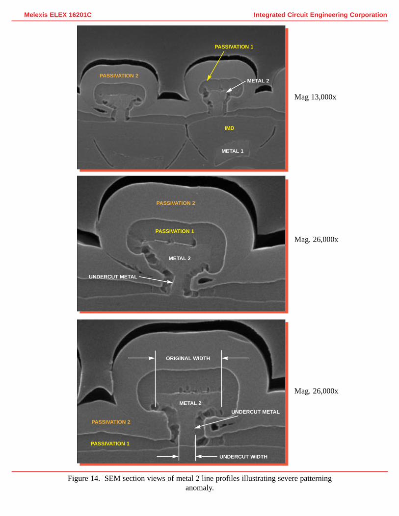
• Metal 2 was severly overetched apparently during patterning which reduced original
line widths by 80 percent (Figures 14-17).
• Metal 1 shorts were noted in the decode circuitry near the SRAM array
(Figures 21-23).
• Metal 1 aluminum also thinned up to 85 percent2 in worst cases. Typical Metal 1
aluminum thinning was 75 percent2.
Note: These metal problems represent some of the most severe processing defects
we’ve analyzed.
Special Features: None.
1These items present possible quality or reliability concerns. They should be discussedwith the manufacturer to determine their possible impact on the intended application.
2Seriousness depends on design margins.

- 2 -
TECHNOLOGY DESCRIPTION
Assembly:
• The devices were packaged in 20-pin Small Outline Integrated Circuit (SOIC)
packages for surface mount applications.
• Lead-locking provisions (holes and/or anchors) at all pins.
• Thermosonic ball bond method employing 1.3 mil O.D. gold wire.
• All pins were connected.
• Die separation by sawn dicing.
• Silver epoxy die attach.
Die Process
• Fabrication process: Selective oxidation CMOS process employing twin-wells in a
P-epi, on a P-substrate.
• Die coat: No die coat was present.
• Overlay passivation: A single layer of nitride over a layer of silicon-dioxide.
• Bonding pads: Both Metal 2 and Metal 1 were used to form the bonding pads.
Metal 2 via arrays were employed along the perimeter of the bond pads.
• Metallization: Two levels of metal were present. Both Metal 2 and 1 consisted of a
layer of aluminum. No cap or barrier metals were employed on either metal. Both
metallization layers were defined by dry-etch techniques. Standard vias and contacts
were used (no plugs).

- 3 -
TECHNOLOGY DESCRIPTION (continued)
• Intermetal dielectric: Two layers of silicon-dioxide. The dielectric layer appeared to have
been subjected to a etchback. Via cuts through this layer appeared to have been wet-etched.
• Pre-metal glass: A reflow glass over a densified oxide. This layer appeared to have been
reflowed following contact cuts.
• Polysilicon: A single layer of poly was used on the die. Poly (no silicide) was used to form
all gates on the die, the word lines and one plate of the capacitors in the EEPROM cell array.
Direct poly-to-diffusion (buried) contacts were not used. Definition of the poly was by a
dry etch.
• Diffusions: Standard implanted N+ and P+ diffusions formed the sources/drains of
transistors. Oxide sidewall spacers were present with the transistors to provide the LDD
spacing and were left in place.
• Local oxide (LOCOS) isolation. A slight step was present in the oxide at the edge of the
well boundaries which indicates a twin-well process was used.
• Wells: Twin-wells in a P-epi, on a P substrate.
• SRAM memory cells: A 6T CMOS SRAM cell design. Poly was used as the word
lines,pull-up devices and storage gates. Metal 1 formed the bit lines and distributed GND
and VCC to each individual cell. Cell size was 14.6 x 23 microns.
• EEPROM cell array: The memory cell consisted of a 3T, single capacitor, EEPROM design.
Metal was used to form the bit lines. Poly was used to form the word/select lines, one plate
of the capacitor and the tunnel-oxide device. Cell size was 13.3 x 35.7 microns.
• ROM cell array: A NAND ROM cell design was employed. Single transistor cell size was
6.2 x 28.8 microns. Implants are used to program the memory cells.

- 4 -
ANALYSIS RESULTS I
Assembly: Figures 1 - 8
Questionable Items:1 None.
General Items:
• Devices were packaged in 20-pin Small Outline Integrated Circuit (SOIC) packages
for surface mount applications.
• Overall package quality: Normal. No defects were found on the external or internal
portions of the packages. Leads were well formed and tinning was complete. No
gaps were noted at lead exits.
• Lead-locking provisions (anchors and/or holes) were present.
• Wirebonding: Thermosonic ball bond method using 1.3 mil O.D. gold wire. No
bond lifts occurred and bond pull strengths were good (see page 11). Wire spacing
and placement was normal.
• Die attach: Silver-epoxy die attach of normal quality. Some small voids were noted
in the epoxy located at the edge of the die, but no problems are foreseen. The die
placement on the header was slightly offset; however, and no problems were noted
(Figure 5a).
• Die dicing: Die separation was by sawing (full depth) with normal quality
workmanship.
1These items present possible quality or reliability concerns. They should be discussed with the manufacturer to determine their possible impact on the intended application.
- 5 -
ANALYSIS RESULTS II
Die Process and Design: Figures 9 - 42
Questionable Items:1
• This device had severe metal patterning problems and proper functioning of the
device is unlikely.
• Metal 2 was severly overetched apparently during patterning which reduced original
line widths by 80 percent (Figures 14-17).
• Metal 1 shorts were noted in the decode circuitry near the SRAM array
(Figures 21-23).
• Metal 1 aluminum also thinned up to 85 percent2 in worst cases. Typical Metal 1
aluminum thinning was 75 percent2.
Note: These metal problems represent some of the most severe processing defects
we’ve analyzed.
Special Features: None.
General Items:
• Fabrication process: Selective oxidation CMOS process employing twin-wells in a
P-epi, on a P substrate.
1These items present possible quality or reliability concerns. They should be discussed with the manufacturer to determine their possible impact on the intended application.
2Seriousness depends on design margins.
- 6 -
ANALYSIS RESULTS II (continued)
• Design and layout: Die layout was clean and efficient. Alignment was good at all
levels.
• Die surface defects: None. No contamination or toolmarks were noted.
• Overlay passivation: A single layer of nitride over a layer of silicon-dioxide.
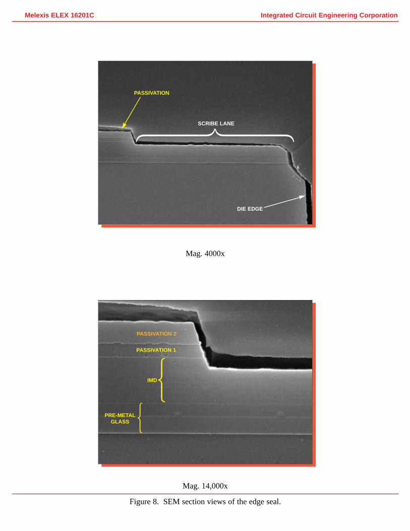
Passivation integrity tests indicated defect-free passivation. Edge seal was good.
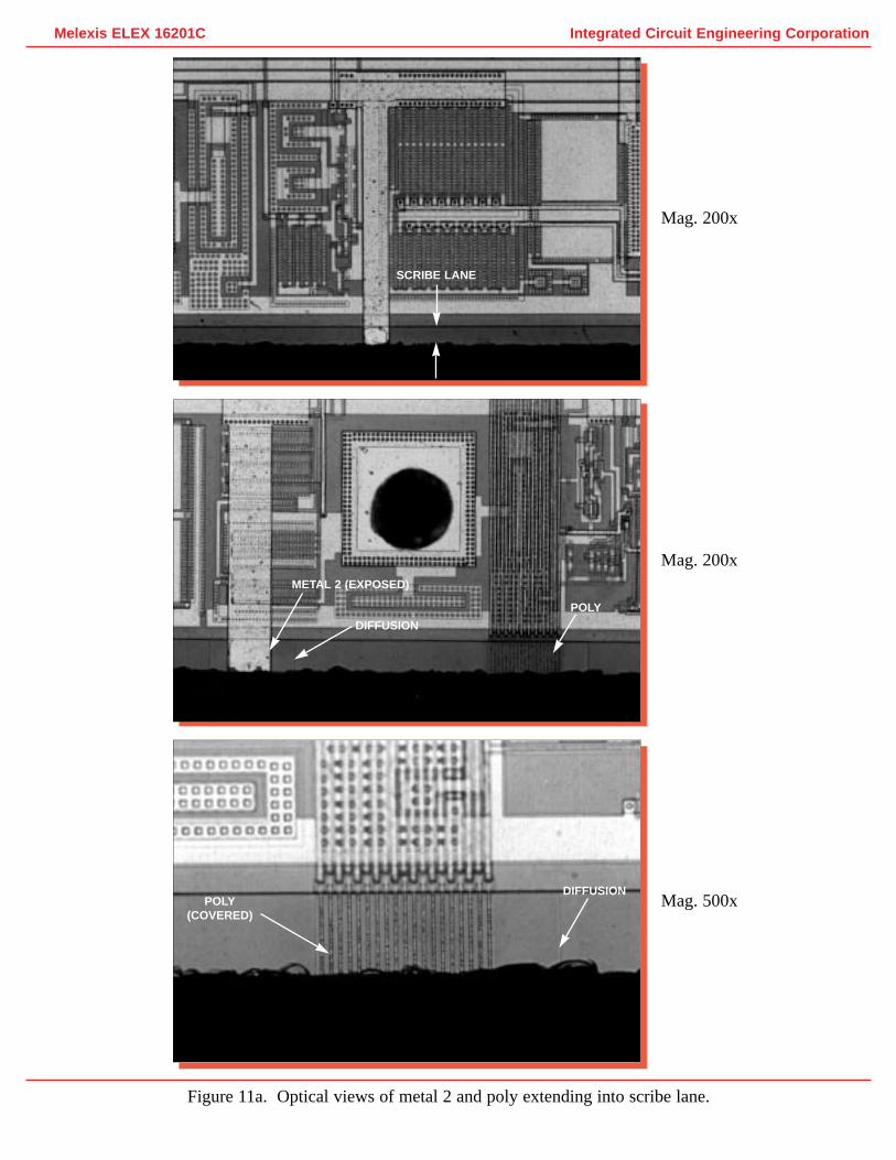
Some active metal 2 lines were carried into the scribe lane and left exposed. (see
Figure 11a). This is unusual since it leaves the active line subjected to contamination
and moisture.
• Metallization: Two levels of metallization. Both Metal 2 and 1 consisted of a layer
of aluminum. No cap or barrier metals were employed on either metal. Metal 1
formed the bit lines within the SRAM, EEPROM, and ROM cell arrays. Standard
vias and contacts were used (no plugs).
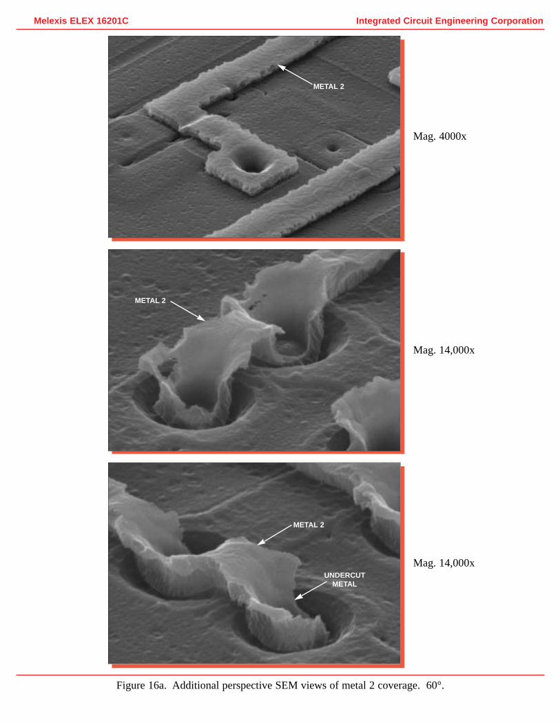
• Metal patterning: Both metal layers were defined by a dry etch. Overetching of the
Metal 2 was apparent. The lack of Metal 2 patterning control resulted in “jadded”
lines which reduced line widths by 80 percent. These anomalies indicate extremely
poor processing control. Although Metal 1 patterning was normal, Metal 1 shorts
were also noted in the decode circuitry near the SRAM array (Figures 21-23), again
illustrating poor processing control. It is highly unlikely that this device would
operate properly. Three of the five devices were decapped and the anomalies were
noted on all three devices.
• Metal defects: Severe patterning anomalies. (See above).
- 7 -
ANALYSIS RESULTS II (continued)
• Metal step coverage: Due to Metal 2 being overetched an accurate measurement of
aluminum thinning could not be performed. Worst case Metal 1 aluminum thinned
up to 85 percent at contact edges. Typical Metal 1 aluminum thinning was 75
percent. MIL-STD allows up to 70 percent metal thinning for contacts of this size.
Metal lines were widened around contacts and contacts were completely surrounded
by metal.
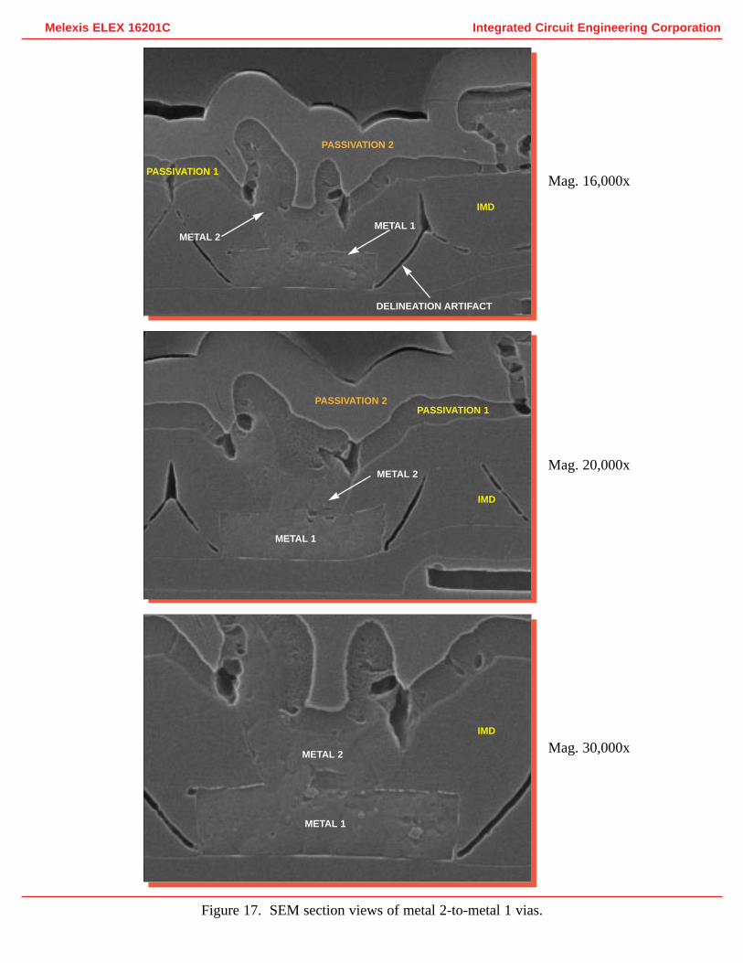
• Contacts: Metal 2 vias and Metal 1 contact cuts appeared to have been wet-etched.
Contacts appeared to be reflowed. Some minor over-etching of the contacts was
present. The contact cuts penetrated up to 40 percent of the polysilicon
thickness and diffusion depths. However, no full penetration through the junctions
was found.
• Intermetal dielectric: Two layers of silicon dioxide. The dielectric layer appeared to
have been subjected to a etchback. Via cuts through this layer appeared to have been
wet-etched.
• Pre-metal glass: A reflow glass over a densified oxide. This layer appeared to have
been reflowed following contact cuts. No problems were found.
• Polysilicon: A single layer of poly was used on the die. Poly (no silicide) was used
to form all gates on the die, the word lines and one plate of the capacitors in the
EEPROM cell array. Definition of the poly was by a dry etch of normal quality.
Poly lines extended into the scribe lane (which is unusual) and the poly appeared to
be covered by the interlevel dielectric (see Figure 11a).
• Isolation: Local oxide (LOCOS) isolation was used. No problems were noted. The slight
step present in the oxide at the well boundary indicates a twin-well process was employed.
The P-well could not be delineated in cross-section.

- 8 -
ANALYSIS RESULTS II (continued)
• Diffusions: Standard implanted N+ and P+ diffusions were used for the
sources/drains of the CMOS transistors. An LDD process was used with oxide
sidewall spacers left in place. No silicide was present over diffusions.
• Wells: Twin-wells in a P-epi, on a P substrate. A step was present in the LOCOS at
the well boundaries.
• Buried contacts: Direct poly-to-diffusion (buried) contacts were not used.
• SRAM memory cells: A 6T CMOS SRAM cell design. Poly was used as the word
lines,pull-up devices and storage gates. Metal 1 formed the bit lines and distributed
GND and VCC to each individual cell. Cell size was 14.6 x 23 microns.
• EEPROM cell array: The memory cell consisted of a 3T, single capacitor, EEPROM
design. Metal was used to form the bit lines. Poly was used to form the word/select
lines, one plate of the capacitor and the tunnel-oxide device. Cell size was 13.3 x
35.7 microns.
• ROM cell array: A NAND ROM cell design was employed. Single transistor cell
size was 6.2 x 28.8 microns. Special implants are used to program the memory
cells.
- 9 -
PROCEDURE
The devices were subjected to the following analysis procedures:
External inspection
X-ray
Package section
Decapsulation
Internal optical inspection
SEM inspection of assembly features and passivation
Passivation integrity test
Wirepull tests
Passivation removal
SEM inspection of metal 2
Delayer to metal 1
SEM inspection of metal 1
Delayer to poly and inspect poly structures and die surface
Die sectioning (90° for SEM)*
Measure horizontal dimensions
Measure vertical dimensions
Die material analysis
*Delineation of cross-sections is by silicon etch unless otherwise indicated.
- 10 -
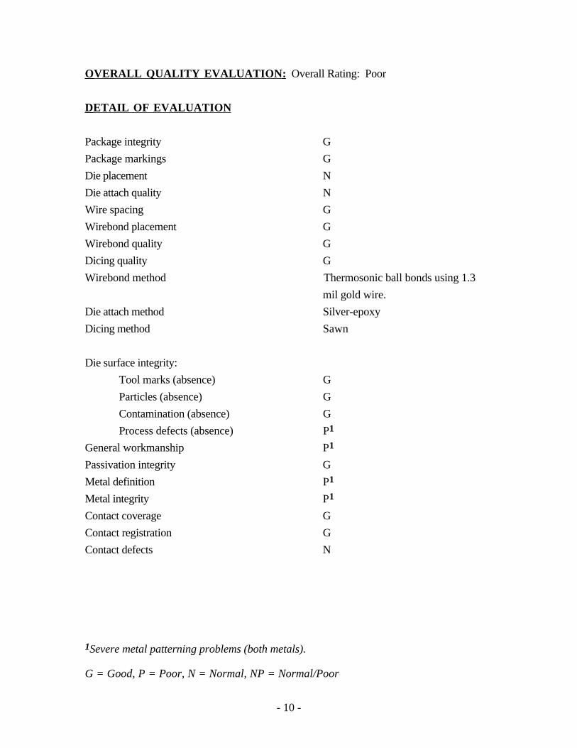
OVERALL QUALITY EVALUATION: Overall Rating: Poor
DETAIL OF EVALUATION
Package integrity G
Package markings G
Die placement N
Die attach quality N
Wire spacing G
Wirebond placement G
Wirebond quality G
Dicing quality G
Wirebond method Thermosonic ball bonds using 1.3
mil gold wire.
Die attach method Silver-epoxy
Dicing method Sawn
Die surface integrity:
Tool marks (absence) G
Particles (absence) G
Contamination (absence) G
Process defects (absence) P1
General workmanship P1
Passivation integrity G
Metal definition P1
Metal integrity P1
Contact coverage G
Contact registration G
Contact defects N
1Severe metal patterning problems (both metals).
G = Good, P = Poor, N = Normal, NP = Normal/Poor
- 11 -
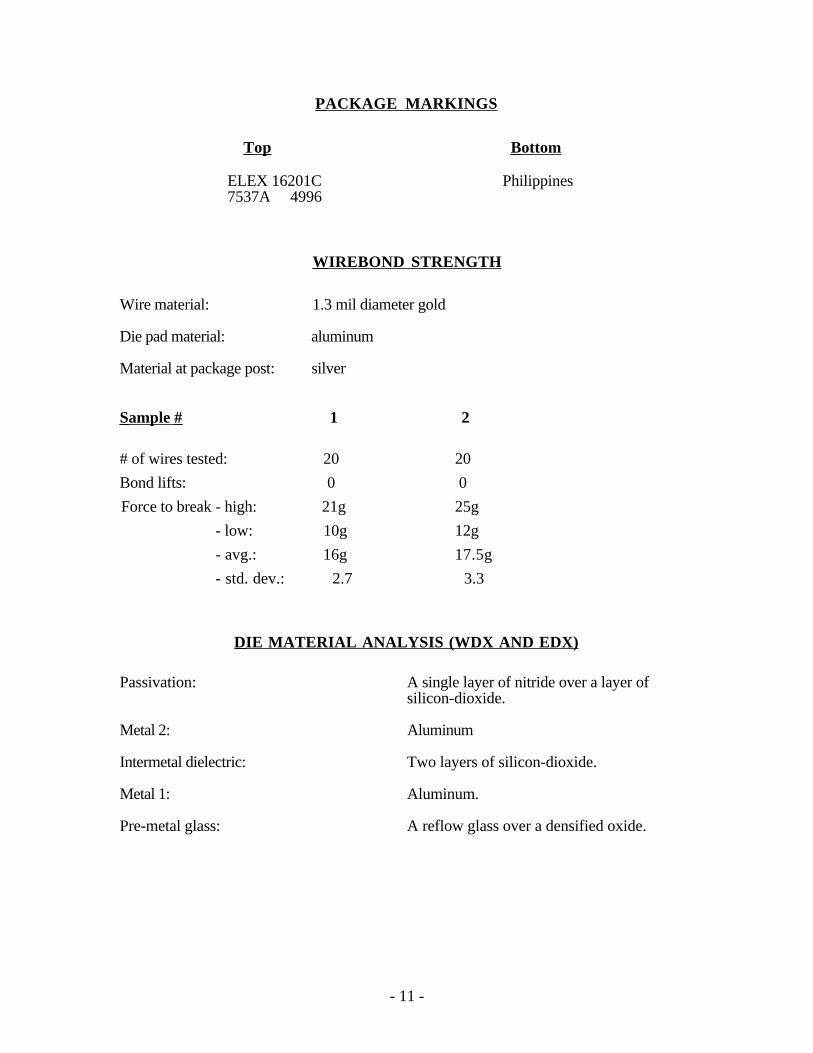
PACKAGE MARKINGS
Top Bottom
ELEX 16201C Philippines7537A 4996
WIREBOND STRENGTH
Wire material: 1.3 mil diameter gold
Die pad material: aluminum
Material at package post: silver
Sample # 1 2
# of wires tested: 20 20
Bond lifts: 0 0
Force to break - high: 21g 25g
- low: 10g 12g
- avg.: 16g 17.5g
- std. dev.: 2.7 3.3
DIE MATERIAL ANALYSIS (WDX AND EDX)
Passivation: A single layer of nitride over a layer ofsilicon-dioxide.
Metal 2: Aluminum
Intermetal dielectric: Two layers of silicon-dioxide.
Metal 1: Aluminum.
Pre-metal glass: A reflow glass over a densified oxide.

- 12 -
HORIZONTAL DIMENSIONS
Die size: 4.4 x 7.2 mm (176 x 287 mils)
Die area: 31.6 mm2 (50,512 mils2)
Min pad size: 0.15 x 0.15 mm (6 x 6 mils)
Min pad window: 0.11 x 0.11 mm (4.7 x 4.7 mils)
Min pad space: 0.5 mm (19.5 mils)
Min pad to metal: 10 microns
Min metal 2 width: 1.35 microns
Min metal 2 space: 2.7 microns
Min via: 1.0 microns (round)
Min metal 1 width: 1.2 micron
Min metal 1 space: 1.4 micron
Min metal 1 pitch: 2.6 microns
Min contact: 1.4 micron (round)
Min poly width: 1.0 micron
Min poly space: 1.3 micron
Min poly pitch: 2.3 microns
Min gate length*- (N-channel): 1.0 micron
- (P-channel): 1.1 micron
EEPROM cell size: 474 microns2
EEPROM cell pitch: 13.3 x 35.7 microns
ROM cell size: 178 microns2
ROM cell pitch: 6.2 x 28.8 microns
SRAM cell size: 335 microns2
SRAM cell pitch: 14.6 x 23 microns
*Physical gate length.

- 13 -
VERTICAL DIMENSIONS
Die thickness: 0.6 mm (25 mils)
Layers
Passivation 2: 0.8 micron
Passivation 1: 0.4 micron
Metallization 2: 1.0 micron
Intermetal dielectric: 1.2 micron
Metallization 1: 0.65 micron
Pre-metal glass: 0.5 micron
Poly: 0.3 micron
Oxide over N+: 0.1 micron
Oxide over P+: 0.09 micron
Local oxide: 0.6 micron
N+ diffusion: 0.55 micron
P+ diffusion: 0.4 micron
N-well: 5.3 microns
P-epi: 13.5 microns

- ii -
INDEX TO FIGURES
PACKAGING AND ASSEMBLY Figures 1 - 8
DIE LAYOUT AND IDENTIFICATION Figures 9 - 11a
PHYSICAL DIE STRUCTURES Figures 12 - 42
COLOR DRAWING OF DIE STRUCTURE Figure 32
EEPROM CELL Figures 33 - 35b
ROM CELL Figures 36 - 38
SRAM CELL Figures 39 - 41
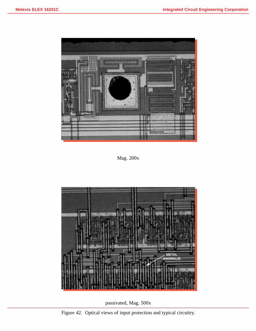
INPUT PROTECTION CIRCUIT Figure 42
GENERAL CIRCUIT LAYOUT Figure 42

Melexis ELEX 16201C
bottom view
top view
Figure 1. Package photographs of the Melexis ELEX 16201C device. Mag. 5.4x.
Integrated Circuit Engineering Corporation
Integrated Circuit Engineering CorporationMelexis ELEX 16201C
side view
top view
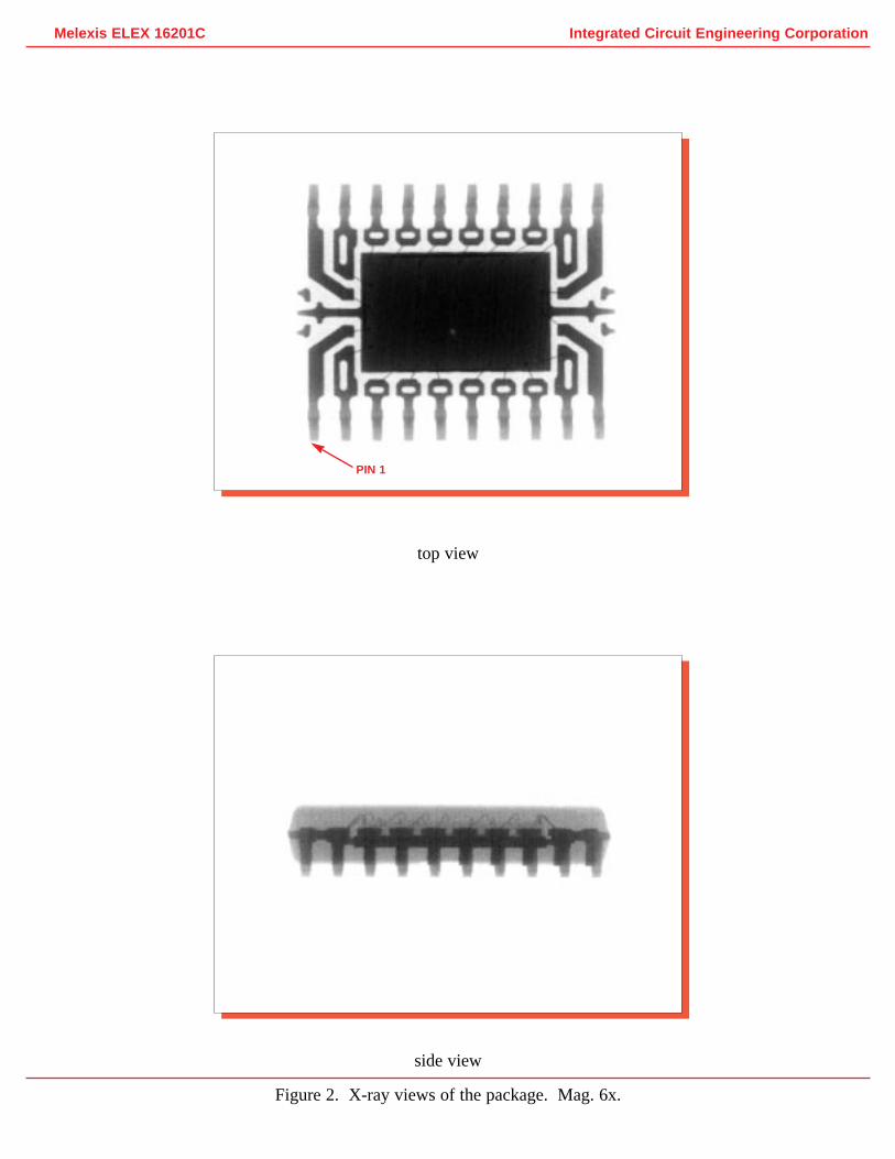
Figure 2. X-ray views of the package. Mag. 6x.
PIN 1

Figure 3. Package section view illustrating general construction. Mag. 25x.
Integrated Circuit E
ngineering Corporation
Melexis E
LEX
16201C
DIE
PLASTIC PACKAGE
HEADER
SECTIONINGARTIFACTLEADFRAME

Mag. 40x
Mag. 100x
Mag. 170x
Integrated Circuit Engineering CorporationMelexis ELEX 16201C
Figure 4. Optical and SEM section views of the leadframe and leadframe exit.
Cu LEADFRAME
LEAD LOCKINGHOLE
PLASTICPACKAGE
PLASTICPACKAGE
SnPb TINNING
SnPb TINNING
Cu LEADFRAME
Cu LEADFRAME
112233

Integrated Circuit Engineering CorporationMelexis ELEX 16201C
Mag. 500x
Mag. 80x
Figure 5. Package section views illustrating dicing and die attach.
DIE
DIE
Cu HEADER
Cu HEADER
VOIDAg EPOXY
Ag PLA TING

Integrated Circuit Engineering CorporationMelexis ELEX 16201C
Figure 5a. Package section views illustrating die placement on header. Mag. 200x.
DIE
Cu HEADER
Cu HEADER
DIE

Integrated Circuit Engineering CorporationMelexis ELEX 16201C
delineated
as polished
Figure 6. Package section views of a typical ball bond. Mag. 800x.
Au
Au
INTERMETALLIC
DIE
DIE

Integrated Circuit Engineering CorporationMelexis ELEX 16201C
Mag. 35x
Mag. 700x
Figure 6a. SEM views of typical wirebonds. 60°.
Au
Au
LEADFRAME
Integrated Circuit Engineering CorporationMelexis ELEX 16201C
Mag. 100x
Mag. 120x
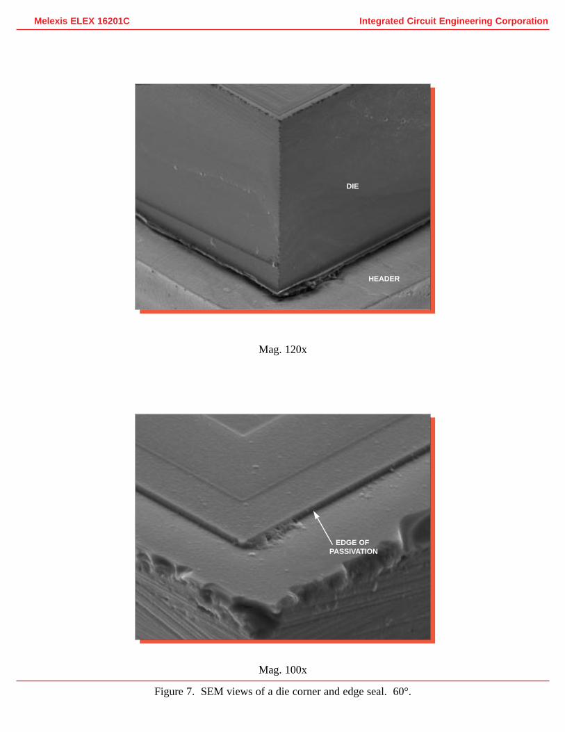
Figure 7. SEM views of a die corner and edge seal. 60°.
EDGE OFPASSIVATION
DIE
HEADER
Integrated Circuit Engineering CorporationMelexis ELEX 16201C
Mag. 14,000x
Mag. 4000x
Figure 8. SEM section views of the edge seal.
PASSIVATION
PASSIVATION 1
PASSIVATION 2
IMD
PRE-METALGLASS
DIE EDGE
SCRIBE LANE 14243
1122
33
1122
33

Integrated Circuit Engineering CorporationMelexis ELEX 16201C
Figure 9. Whole die photograph of the Melexis ELEX 16201C device. Mag. 32x.
PIN 1
Integrated Circuit Engineering CorporationMelexis ELEX 16201C
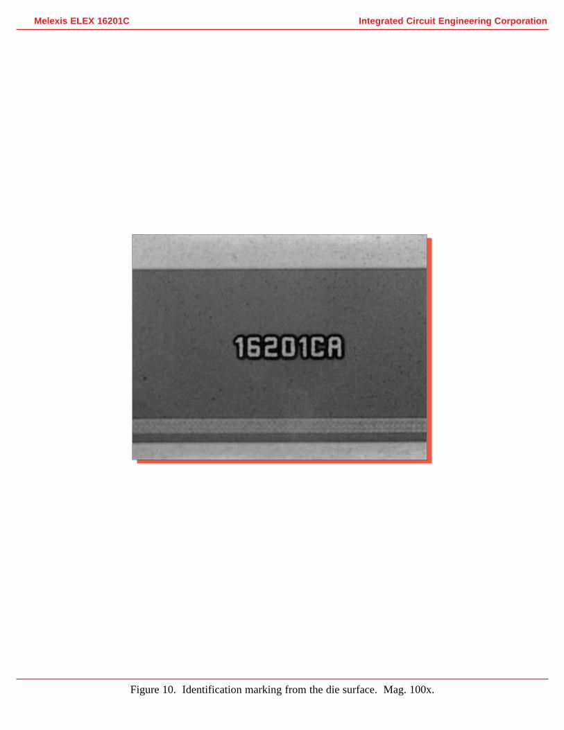
Figure 10. Identification marking from the die surface. Mag. 100x.
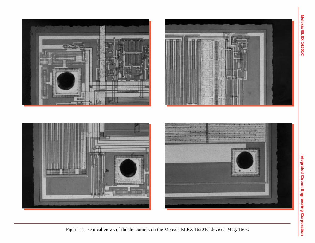
Figure 11. Optical views of the die corners on the Melexis ELEX 16201C device. Mag. 160x.
Integrated Circuit E
ngineering Corporation
Melexis E
LEX
16201C
Mag. 200x
Mag. 200x
Mag. 500x
Integrated Circuit Engineering CorporationMelexis ELEX 16201C
Figure 11a. Optical views of metal 2 and poly extending into scribe lane.
SCRIBE LANE
POLY
POLY(COVERED)
DIFFUSION
DIFFUSION
METAL 2 (EXPOSED)

Integrated Circuit Engineering CorporationMelexis ELEX 16201C
Figure 12. SEM section views illustrating general device structure. Mag. 13,000x.
PASSIVATION 2
PASSIVATION 2
PASSIVATION 1
PASSIVATION 1
METAL 2
METAL 2
METAL 1
UNDERCUT METAL
METAL 1
DELINEATION ARTIFACTS
UNDERCUT METAL
N+ S/D
METAL 2
POLY
POLY
IMD
IMD
PRE-METAL GLASS
PRE-METAL GLASS
LOCAL OXIDE

Mag. 5000x
Mag. 10,000x
Mag. 13,500x
Integrated Circuit Engineering CorporationMelexis ELEX 16201C
Figure 13. SEM views of overlay passivation coverage illustrating metal 2 patterninganomaly below. 60°.
METAL 2PATTERNING
ANOMALY
Mag 13,000x
Mag. 26,000x
Mag. 26,000x
Integrated Circuit Engineering CorporationMelexis ELEX 16201C
Figure 14. SEM section views of metal 2 line profiles illustrating severe patterninganomaly.
PASSIVATION 2
PASSIVATION 2
PASSIVATION 2
PASSIVATION 1
PASSIVATION 1
PASSIVATION 1
METAL 2
METAL 2
UNDERCUT METAL
METAL 2
ORIGINAL WIDTH
UNDERCUT WIDTH
UNDERCUT METAL
IMD
METAL 1

Mag. 5000x
Mag. 8000x
Mag 10,000x
Integrated Circuit Engineering CorporationMelexis ELEX 16201C
Figure 15. Topological SEM views illustrating metal 2 patterning anomaly. 0°.
METAL 2
METAL 2
METAL 2
WIDTH 0.6µ
ORIGINAL LINEWIDTH 1.4µ

Mag. 4000x
Mag. 8000x
Mag. 16,000x
Integrated Circuit Engineering CorporationMelexis ELEX 16201C
Figure 16. Perspective SEM views illustrating metal 2 coverage. 60°.
METAL 2
METAL 2
METAL 2
UNDERCUT METAL
VIA
Mag. 4000x
Mag. 14,000x
Mag. 14,000x
Integrated Circuit Engineering CorporationMelexis ELEX 16201C
Figure 16a. Additional perspective SEM views of metal 2 coverage. 60°.
METAL 2
METAL 2
METAL 2
UNDERCUTMETAL
Mag. 16,000x
Mag. 20,000x
Mag. 30,000x
Integrated Circuit Engineering CorporationMelexis ELEX 16201C
Figure 17. SEM section views of metal 2-to-metal 1 vias.
PASSIVATION 2
PASSIVATION 2
IMD
IMD
IMD
METAL 1
METAL 1
METAL 1
METAL 2
DELINEATION ARTIFACT
METAL 2
METAL 2
PASSIVATION 1
PASSIVATION 1
Integrated Circuit Engineering CorporationMelexis ELEX 16201C
Mag. 30,000x
Mag. 20,000x
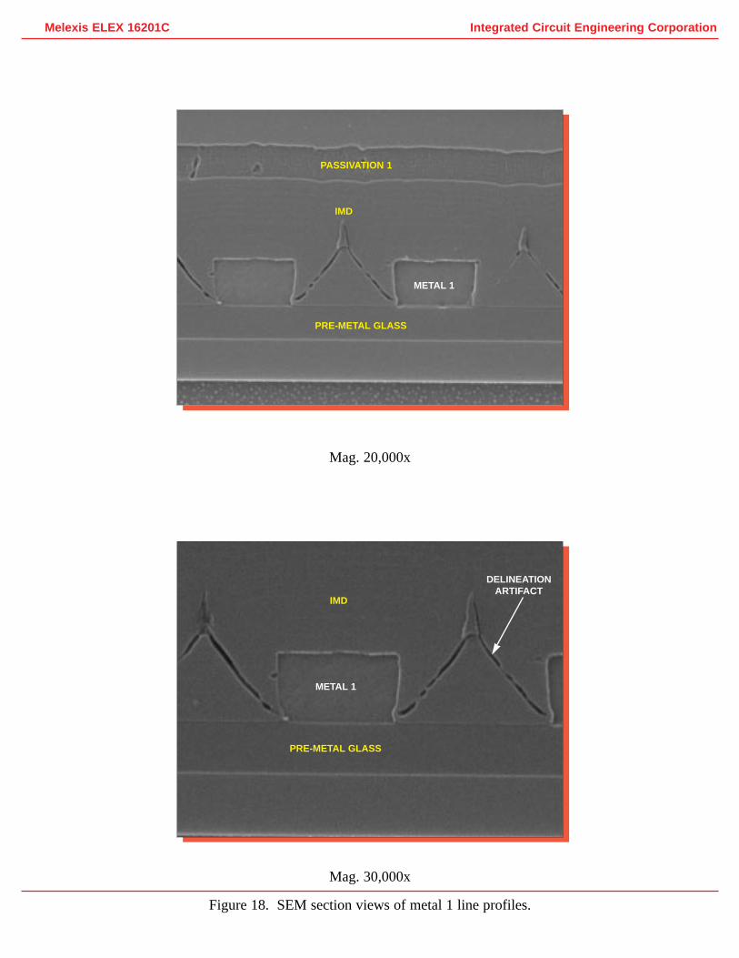
Figure 18. SEM section views of metal 1 line profiles.
PASSIVATION 1
IMD
IMD
METAL 1
METAL 1
DELINEATIONARTIFACT
PRE-METAL GLASS
PRE-METAL GLASS

Mag. 3300x
Mag. 3300x
Mag. 8000x
Integrated Circuit Engineering CorporationMelexis ELEX 16201C
Figure 19. Topological SEMviews illustrating metal 1 patterning. 0°.
METAL 1
METAL 1
METAL 1CONTACTS
Mag. 3300x
Mag. 5700x
Mag. 16,000x
Integrated Circuit Engineering CorporationMelexis ELEX 16201C
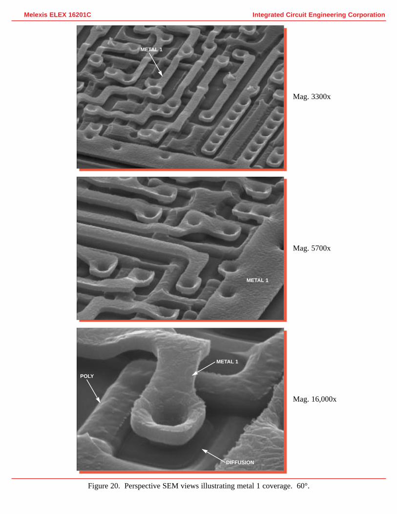
Figure 20. Perspective SEM views illustrating metal 1 coverage. 60°.
METAL 1
METAL 1
METAL 1
DIFFUSION
POLY
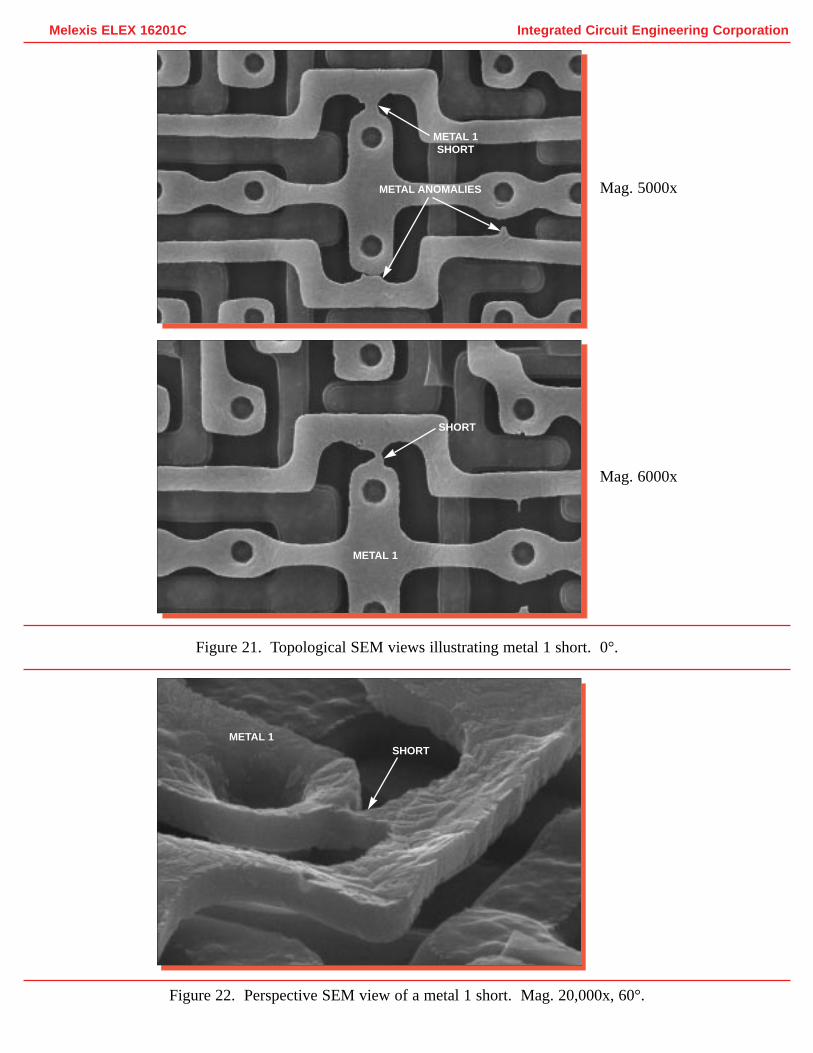
Figure 21. Topological SEM views illustrating metal 1 short. 0°.
Mag. 5000x
Mag. 6000x
Integrated Circuit Engineering CorporationMelexis ELEX 16201C
Figure 22. Perspective SEM view of a metal 1 short. Mag. 20,000x, 60°.
METAL 1SHORT
METAL ANOMALIES
METAL 1
METAL 1
SHORT
SHORT
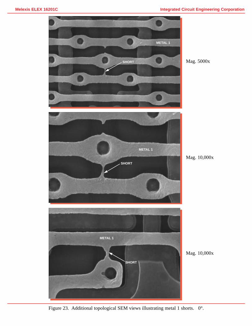
Mag. 5000x
Mag. 10,000x
Mag. 10,000x
Integrated Circuit Engineering CorporationMelexis ELEX 16201C
Figure 23. Additional topological SEM views illustrating metal 1 shorts. 0°.
METAL 1
METAL 1
METAL 1
SHORT
SHORT
SHORT

metal 1-to-N+,Mag. 20,000x
metal 1-to-P+,Mag. 20,000x
metal 1-to-P+,Mag. 26,000x
Integrated Circuit Engineering CorporationMelexis ELEX 16201C
Figure 24. SEM section views of metal 1-to-diffusion contacts.
PASSIVATION 1
IMD
IMD
IMD
POLY
POLY
POLY
N+
P+
P+
METAL 1
METAL 1
METAL 1
THINNING
PRE-METALGLASS
PRE-METALGLASS
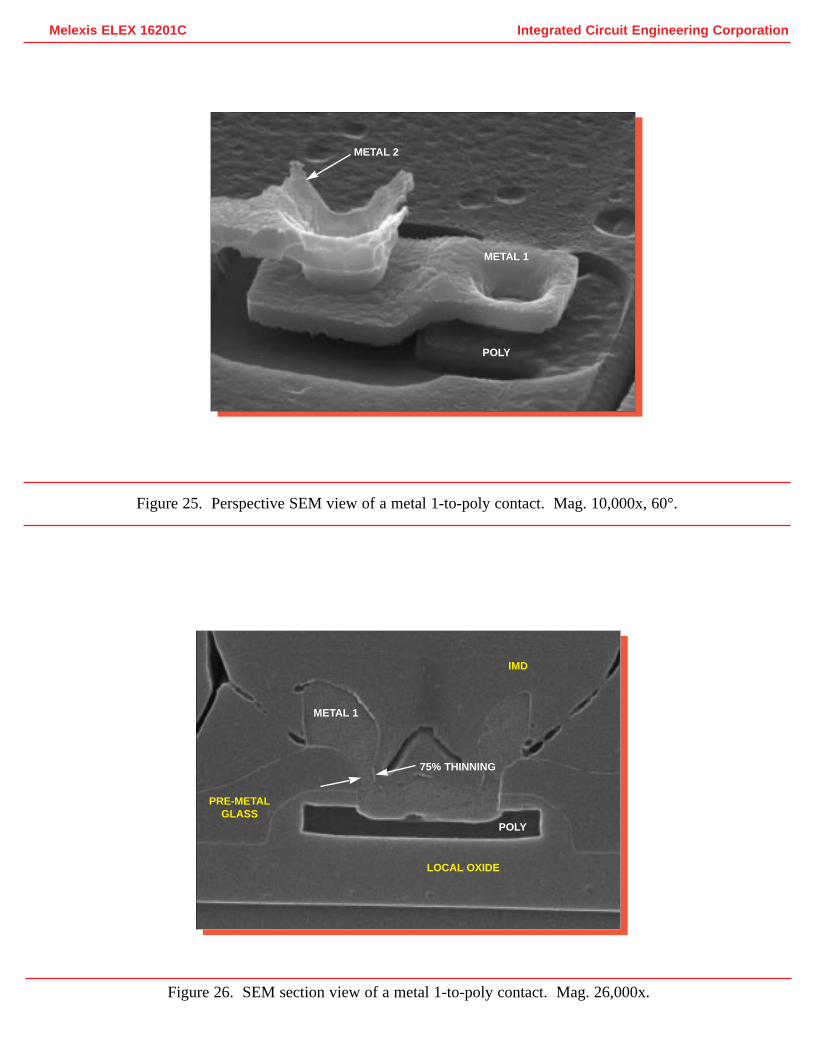
Figure 25. Perspective SEM view of a metal 1-to-poly contact. Mag. 10,000x, 60°.
Figure 26. SEM section view of a metal 1-to-poly contact. Mag. 26,000x.
Integrated Circuit Engineering CorporationMelexis ELEX 16201C
METAL 2
METAL 1
METAL 1
75% THINNING
PRE-METALGLASS
LOCAL OXIDE
IMD
POLY
POLY

Mag. 2000x
Mag. 3300x
Mag. 3300x
Integrated Circuit Engineering CorporationMelexis ELEX 16201C
Figure 27. Topological SEM views illustrating poly patterning. 0°.
P+
POLY
POLY
POLY CAPPOLYCAP
DIFFUSION
DIFFUSION
N+
Integrated Circuit Engineering CorporationMelexis ELEX 16201C
Mag. 16,000x
Mag. 4000x
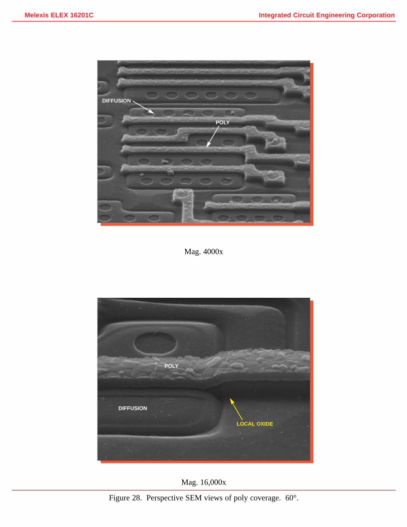
Figure 28. Perspective SEM views of poly coverage. 60°.
DIFFUSION
DIFFUSION
LOCAL OXIDE
POLY
POLY

Integrated Circuit Engineering CorporationMelexis ELEX 16201C
P-channel
N-channel
Figure 29. SEM section views of typical transistors. Mag. 26,000x.
IMD
IMD
POLY
POLY
GATE OXIDE
GATE OXIDE
N+ S/D
P+ S/D
METAL 1PRE-METAL GLASSSIDEWALL SPACER
SIDEWALL SPACER

Figure 30. SEM section view of a local oxide birdsbeak. Mag. 30,000x.
Figure 31. SEM section view of the step in the local oxide at the well boundary. Mag. 40,000x.
Integrated Circuit Engineering CorporationMelexis ELEX 16201C
IMD
IMD
GATE OXIDE
LOCAL OXIDE
LOCAL OXIDE
PRE-METAL GLASS
PRE-METAL GLASS
BIRDSBEAK
POLY
STEP
Integrated Circuit Engineering CorporationMelexis ELEX 16201C
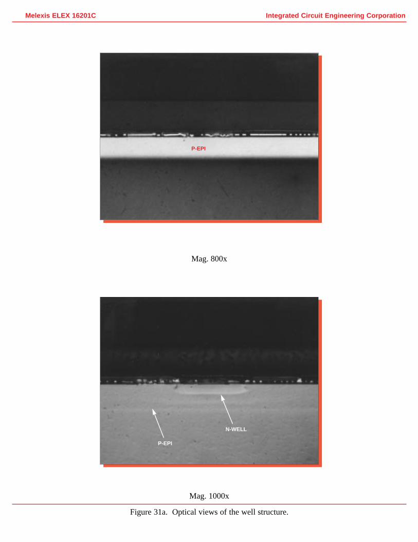
Mag. 1000x
Mag. 800x
Figure 31a. Optical views of the well structure.
P-EPI
N-WELL
P-EPI

Figure 32 . Color cross section drawing illustrating device structure.
Orange = Nitride, Blue = Metal, Yellow = Oxide, Green = Poly,
Red = Diffusion, and Gray = Substrate
Integrated Circuit E
ngineering Corporation
Melexis E
LEX
16201C
������������������������������������������������������
� ��
P-EPI
GATE OXIDE
LOCAL OXIDE
P+ S/D N-WELL
P-WELL
N+ S/D
INTERMETAL GLASS 2
INTERMETAL GLASS 1
PRE-METAL GLASS
POLY
METAL 1
METAL 2PASSIVATION 1
PASSIVATION 2
P SUBSTRATE
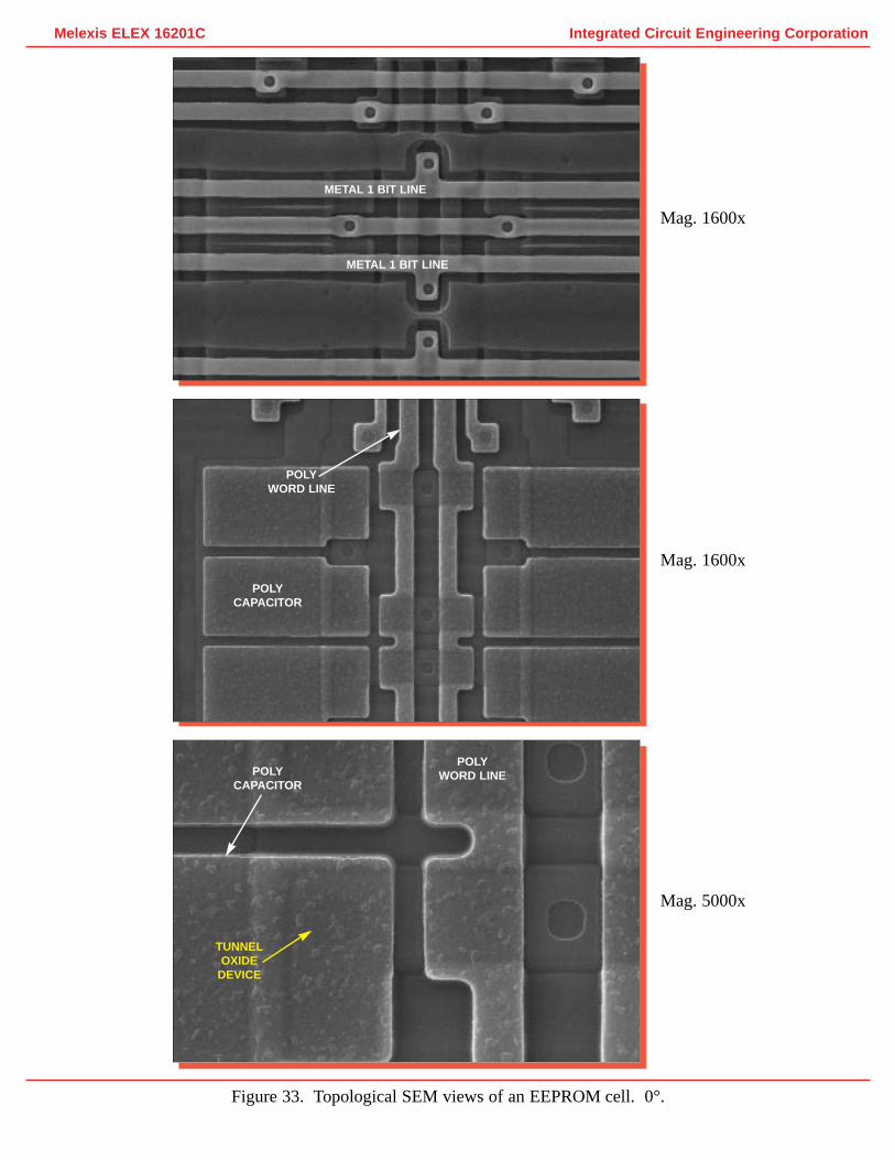
Mag. 1600x
Mag. 1600x
Mag. 5000x
Integrated Circuit Engineering CorporationMelexis ELEX 16201C
Figure 33. Topological SEM views of an EEPROMcell. 0°.
METAL 1 BIT LINE
METAL 1 BIT LINE
POLYCAPACITOR
POLYCAPACITOR
TUNNELOXIDE
DEVICE
POLYWORD LINE
POLYWORD LINE

Mag. 2500x
Mag. 2500x
Mag. 5000x
Integrated Circuit Engineering CorporationMelexis ELEX 16201C
Figure 34. Perspective SEM views of an EEPROM cell. 60°.
METAL 1 BIT LINE
METAL 1 BIT LINE
POLY CAPACITOR
POLYCAPACITOR
POLY WORD LINE
POLY WORD LINE
TUNNEL OXIDE DEVICE
TUNNEL OXIDE DEVICE
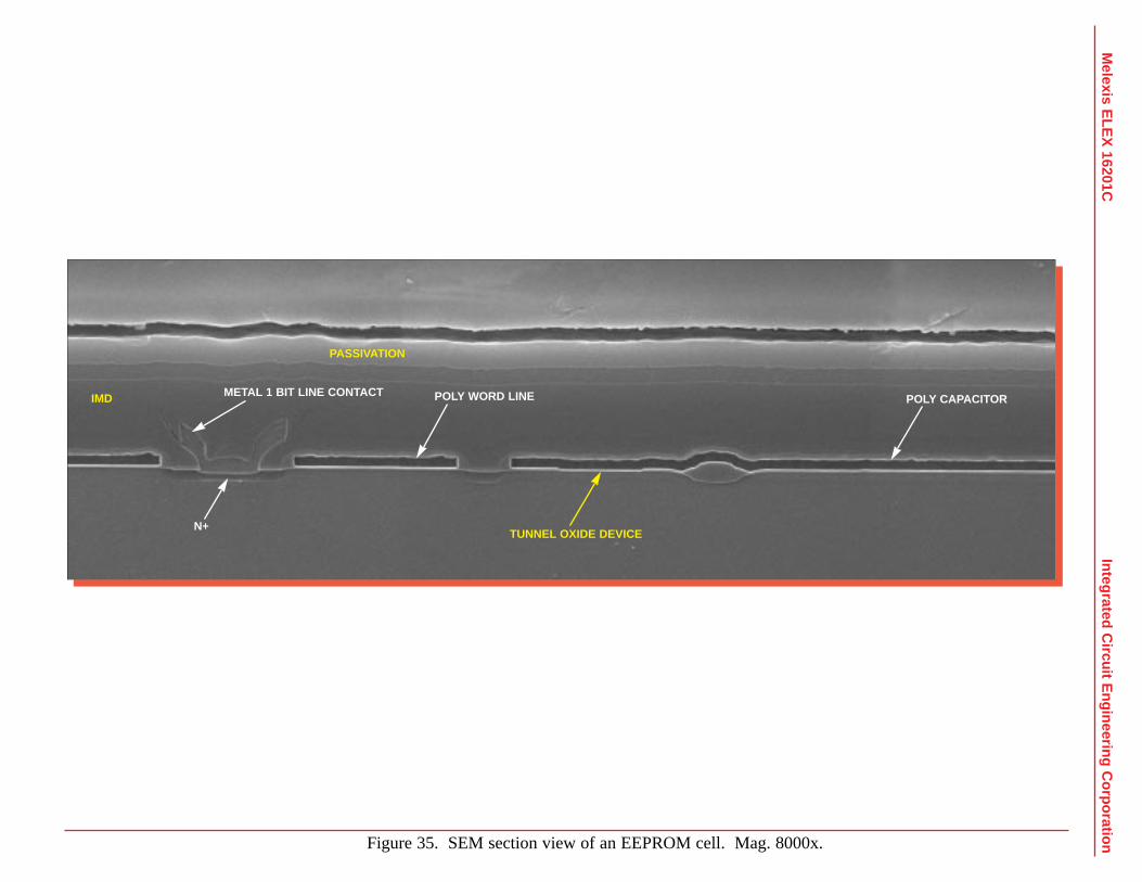
Figure 35. SEM section view of an EEPROM cell. Mag. 8000x.
Integrated Circuit E
ngineering Corporation
Melexis E
LEX
16201C
IMD
N+
METAL 1 BIT LINE CONTACT
PASSIVATION
POLY WORD LINE
TUNNEL OXIDE DEVICE
POLY CAPACITOR

Mag. 14,000x
Mag. 20,000x
Figure 35a. SEM section views of an EEPROM cell illustrating bit line contact andword line.
Integrated Circuit Engineering CorporationMelexis ELEX 16201C
IMD
N+
N+
METAL 1BIT CONTACT
POLY WORDLINE
POLY WORD LINE
GATE OXIDE
SIDEWALLSPACER

Integrated Circuit Engineering Corporation
Mag. 40,000x
Mag. 16,000x
Figure 35b. SEM section views of an EEPROM cell illustrating tunnel oxide device.
Melexis ELEX 16201C
POLY
POLY
GATE OXIDE TUNNEL OXIDE
PRE-METAL GLASS
TUNNEL OXIDE DEVICE
LOCOS
N+

Mag. 1600x
Mag. 3300x
Mag. 3300x
Integrated Circuit Engineering CorporationMelexis ELEX 16201C
Figure 36. Topological SEM views of the ROM array. 0°.
METAL 1 BIT LINE
METAL 1 BIT LINE
POLY
POLY

Integrated Circuit Engineering CorporationMelexis ELEX 16201C
Figure 37. Perspective SEM views of the ROM cell array. Mag. 5000x, 60°.
METAL 1BIT LINE
LOCALOXIDE
POLY WORDLINEDIFFUSION
Integrated Circuit Engineering CorporationMelexis ELEX 16201C
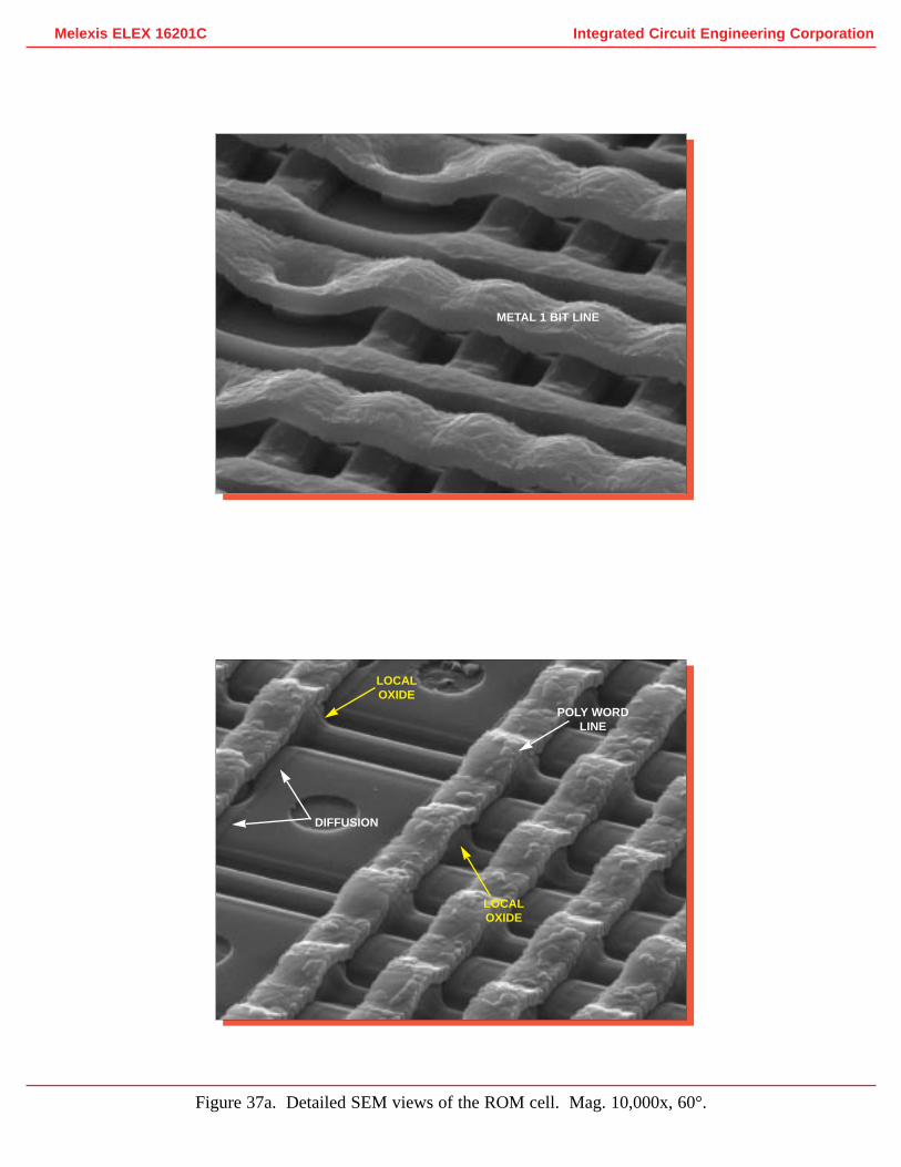
Figure 37a. Detailed SEM views of the ROM cell. Mag. 10,000x, 60°.
METAL 1 BIT LINE
LOCALOXIDE
POLY WORDLINE
LOCALOXIDE
DIFFUSION

Mag. 13,000x
Mag. 13,000x
Mag. 26,000x
Integrated Circuit Engineering CorporationMelexis ELEX 16201C
Figure 38. SEM section views of the ROM array.
IMD
POLY
POLY
GATE OXIDE
POLY
N+
N+
SIDEWALLSPACER
PRE-METAL GLASS
PRE-METAL GLASS
N+ DIFFUSIONACTIVE CHANNEL
IMPLANTEDCHANNEL
Integrated Circuit Engineering CorporationMelexis ELEX 16201C
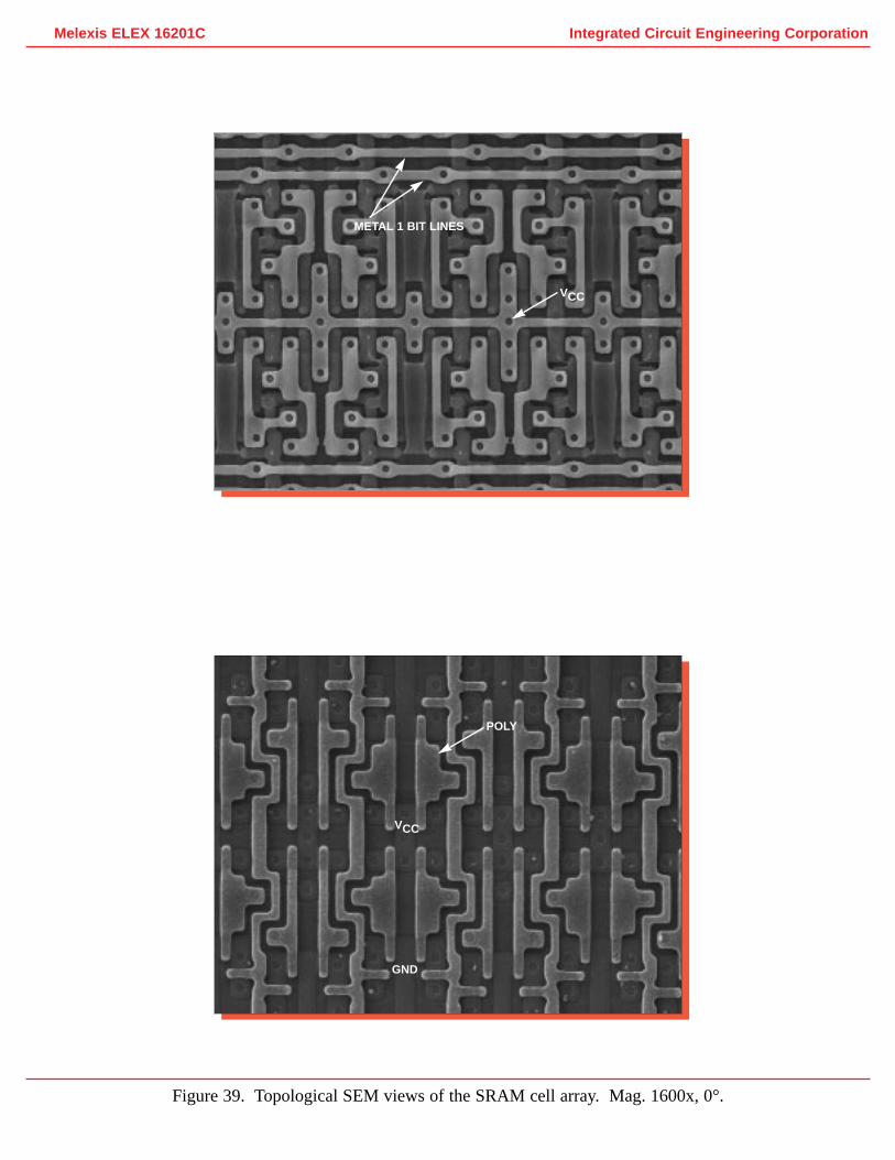
Figure 39. Topological SEM views of the SRAM cell array. Mag. 1600x, 0°.
METAL 1 BIT LINES
VCC
VCC
POLY
GND

Integrated Circuit Engineering CorporationMelexis ELEX 16201C
Figure 40. Perspective SEM views of the SRAMcell array. Mag 3300x, 60°.
BIT LINES
METAL 1
POLY
POLY WORDLINE
Integrated Circuit Engineering CorporationMelexis ELEX 16201C
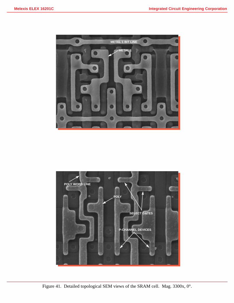
Figure 41. Detailed topological SEM views of the SRAM cell. Mag. 3300x, 0°.
METAL 1 BIT LINE
POLY WORD LINE
METAL 1
POLY
SELECT GATES
P-CHANNEL DEVICES
Integrated Circuit Engineering CorporationMelexis ELEX 16201C
passivated, Mag. 500x
Mag. 200x
Figure 42. Optical views of input protection and typical circuitry.
METALANOMALIE
Related Documents