Medium Voltage Frequency Inverter MVW-01 User's Manual Motors I Automation I Energy I Transmission & Distribution I Coatings

Welcome message from author
This document is posted to help you gain knowledge. Please leave a comment to let me know what you think about it! Share it to your friends and learn new things together.
Transcript
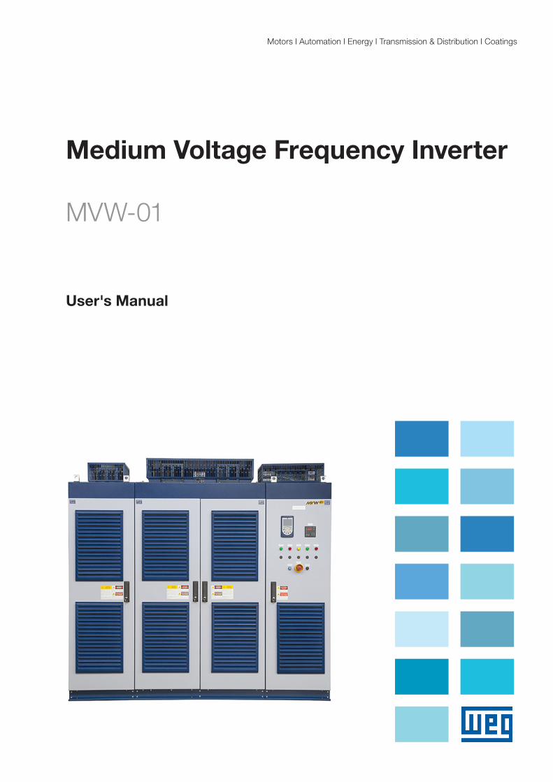
Medium Voltage Frequency Inverter
MVW-01
User's Manual
Motors I Automation I Energy I Transmission & Distribution I Coatings


User's Manual
Series: MVW-01
Language: English
Document: 0899.5247 / 03
Publication Date: 09/2015
Summary of Reviews
Version Review Description
- R01 First edition.
- R02
Addition of the functions:Vector control with encoder.Sensorless vector control.Ride-Through for vector control.Redundant ventilation.Multivariable read-only parameter.WEG protocol at 192000 bps and 38400 bps.Communication protocol for DeviceNet Drive Profile Board.New parameters, new faults and alarms regarding the 4000 HP parallel “Frame C”.General revision.
- R03
Update for the MVW-01 G2 line, firmware version 3.3X.Inclusion of the graphic HMI.Inclusion of the MVW-01C (compact).Inclusion of the 5 level MVW-01.Inclusion of inverter parallelism.Inclusion of the synchronous motor line.Description of special functions.General revision.

Contents
QUICK PARAMETER REFERENCE, FAULTS AND STATUS MESSAGES 0-1I. Parameter .......................................................................................................................................... 0-1II. Messages of Alarms and Faults .................................................................................................. 0-25
1 SAFETY NOTICES .................................................................................. 1-11.1 SAFETY NOTICES IN THE MANUAL .............................................................................................1-11.2 SAFETY NOTICES ON THE PRODUCT .........................................................................................1-11.3 MVW-01 IDENTIFICATION LABEL ................................................................................................1-21.4 PRELIMINARY RECOMMENDATIONS ..........................................................................................1-2
2 GENERAL INFORMATION .....................................................................2-12.1 ABOUT THIS MANUAL ...................................................................................................................2-12.2 SOFTWARE VERSION ....................................................................................................................2-12.3 HOW TO SPECIFY THE MVW-01 MODEL ................................................................................... 2-2
2.3.1 Available Models .................................................................................................................. 2-32.3.2 MVW-01 Main Components ............................................................................................... 2-82.3.3 MVW-01 Electronic boards ...............................................................................................2-112.3.4 PLC2 Expansion Board ......................................................................................................2-11
2.4 RECEIVING AND STORAGE ........................................................................................................2-11
3 MVW-01 WITH 3 LEVELS (3L) ................................................................3-13.1 MECHANICAL DATA ...................................................................................................................... 3-3
3.1.1 Panel Constructive Aspects ............................................................................................... 3-33.2 INPUT RECTIFIER .......................................................................................................................... 3-43.3 INVERTER ARMS ........................................................................................................................... 3-53.4 CONTROL RACK .......................................................................................................................... 3-73.5 OUTPUT FILTERS .......................................................................................................................... 3-8
3.5.1 Sinusoidal Output Filter ...................................................................................................... 3-93.6 AVAILABLE MODELS ...................................................................................................................3-10
4 MVW-01 WITH 5 LEVELS (5L) ................................................................4-14.1 MECHANICAL DATA ...................................................................................................................... 4-24.2 AVAILABLE MODELS .................................................................................................................... 4-2
5 MVW-01C (COMPACT) ...........................................................................5-15.1 PANEL CONSTRUCTIVE DETAILS ............................................................................................... 5-65.2 AVAILABLE MODELS .................................................................................................................... 5-7
6 INVERTER PARALLELISM .....................................................................6-16.1 STRUCTURE OF THE PARALLEL INVERTER ............................................................................ 6-16.2 THREE LEVEL (3L) LINE WITH UP TO FOUR SET PARALLELISM (3L4) .................................. 6-16.3 PARALLELISM OF 2 FRAME D OR 2 FRAME E WITH MASTER/SLAVE RACK ....................... 6-26.4 FIVE LEVEL (5L) PARALLELISM LINE ......................................................................................... 6-4
7 SYNCHRONOUS MOTOR LINE ............................................................. 7-17.1 ABSOLUTE ENCODER WITH RSSI BOARD ..................................................................................7-1
7.1.1 Absolute Encoder ..................................................................................................................7-17.1.2 RSSI Board .............................................................................................................................7-2
7.2 FIELD EXCITATION SET (DC WITH BRUSHES) ...........................................................................7-3

Contents
8 INSTALLATION, CONNECTION AND ENERGIZATION ........................8-18.1 MECHANICAL INSTALLATION ..................................................................................................... 8-1
8.1.1 Environmental Conditions .................................................................................................. 8-18.1.2 Handling Recommendations .............................................................................................. 8-28.1.3 Hoisting ................................................................................................................................. 8-28.1.4 Moving ................................................................................................................................... 8-38.1.5 Unpacking ............................................................................................................................. 8-38.1.6 Positioning/Mounting .......................................................................................................... 8-58.1.7 Power Arm Insertion ............................................................................................................ 8-68.1.8 Power Arm Electric and Fiber Optic Connections ........................................................... 8-88.1.9 Insertion of the MVW-01C Power Arms ............................................................................ 8-9
8.2 ELECTRICAL INSTALLATION ......................................................................................................8-128.2.1 Power Section .....................................................................................................................8-128.2.2 Input Circuit Breaker .........................................................................................................8-158.2.3 Low Voltage Auxiliary Supply ...........................................................................................8-16
8.3 ENERGIZATION, START-UP AND SAFE DE-ENERGIZATION ..................................................8-178.3.1 Pre-power Checks ..............................................................................................................8-178.3.2 Initial Power-up (Parameter Settings) .............................................................................8-188.3.3 Start-up ...............................................................................................................................8-18
8.3.3.1 Start-up with HMI Operation and V/F 60 Hz Control Mode ...............................8-188.3.4 Safe De-energization Instructions ...................................................................................8-19
9 KEYPAD (HMI) OPERATION ..................................................................9-19.1 INSTALLATION OF THE GRAPHIC HMI IN THE CABINET ......................................................... 9-29.2 STARTING THE USE OF THE GRAPHIC HMI .............................................................................. 9-2
9.2.1 Graphic HMI Basic Visualization Modes .......................................................................... 9-39.2.2 Structure of the Parameter Groups .................................................................................. 9-49.2.3 Sequential Access Mode .................................................................................................... 9-59.2.4 Parameter Groups Access Mode ...................................................................................... 9-6
9.3 PARAMETER EDITION .................................................................................................................. 9-79.3.1 Numerical ............................................................................................................................. 9-79.3.2 Alphanumerical.................................................................................................................... 9-7
9.4 CONFIGURING THE GRAPHIC HMI ............................................................................................. 9-89.4.1 LCD Contrast ........................................................................................................................ 9-89.4.2 Configuring the HMI Commands ....................................................................................... 9-89.4.3 Configuring the Monitoring Mode Read-Only Parameters ............................................ 9-89.4.4 Configuring the On-Line Graphic (Watch) Function........................................................ 9-9
9.5 ALARMS AND FAULTS .................................................................................................................9-109.5.1 Alarm/Fault Screen .............................................................................................................9-109.5.2 Note Screen ........................................................................................................................9-109.5.3 Error Log..............................................................................................................................9-11
9.6 HELP FUNCTION ..........................................................................................................................9-12
10 OPTIONAL ACCESSORIES AND BOARDS ......................................10-110.1 MVC4 SIGNAL AND CONTROL CONNECTIONS .....................................................................10-110.2 FUNCTION EXPANSION BOARDS .......................................................................................... 10-4
10.2.1 EBA (I/O Expansion Board A) ......................................................................................... 10-510.2.2 EBB (I/O Expansion Board B) ......................................................................................... 10-810.2.3 PLC2 .................................................................................................................................10-12
10.3 INCREMENTAL ENCODER ......................................................................................................10-1310.3.1 EBA/EBB Boards ............................................................................................................10-1310.3.2 EBC1 Board .....................................................................................................................10-15
10.4 SHORT UPS MODULE ...........................................................................................................10-1810.4.1 CFW10 Inverter Parameterization .................................................................................10-18
10.5 MVC3 CONTROL BOARD CONNECTIONS .............................................................................10-19
Contents
11 DETAILED PARAMETER DESCRIPTION ........................................... 11-111.1 ACCESS AND READ ONLY PARAMETERS - P000 to P099 ....................................................11-111.2 REGULATION PARAMETERS - P100 to P199 ......................................................................... 11-1611.3 CONFIGURATION PARAMETERS - P200 to P399 .................................................................11-3511.4 MOTOR PARAMETERS - P400 TO P489 .................................................................................11-8111.5 PARAMETERS OF THE SYNCHRONOUS MOTOR - P427 TO P465 .....................................11-8311.6 PARAMETER OF THE GRAPHIC HMI - P490 TO P519 ..........................................................11-9011.7 PARAMETERS OF THE PID FUNCTION - P520 TO P535 ......................................................11-9211.8 PARAMETERS OF THE TRACE FUNCTION............................................................................11-9611.9 PARAMETERS OF THE MVC3 ANALOG OUTPUTS - P652 TO P666 .................................11-10211.10 PARAMETERS OF THE MVC4 ANALOG INPUT AI5 ...........................................................11-10411.11 OTHER MVW-01 PARAMETERS ..........................................................................................11-104
12 SPECIAL FUNCTIONS ........................................................................ 12-112.1 Trace Function ............................................................................................................................12-1
12.1.1 Trigger ................................................................................................................................12-112.1.2 Data Access .......................................................................................................................12-112.1.3 Memory ..............................................................................................................................12-212.1.4 Sampling ........................................................................................................................... 12-312.1.5 Pre-Trigger ........................................................................................................................ 12-312.1.6 Trace Function Use and Programming Example ......................................................... 12-412.1.7 Example of Use and Trigger Configuration .................................................................. 12-5
12.2 PID Regulator ............................................................................................................................. 12-612.3 LOAD SHARE FUNCTION "MASTER/SLAVE"......................................................................... 12-912.4 SYNCHRONOUS TRANSFER OR SYNCHRONOUS BYPASS FUNCTION ...........................12-1112.5 SAFETY STOP FUNCTION .......................................................................................................12-13
13 COMMUNICATION NETWORKS ........................................................13-113.1 FIELDBUS KIT .............................................................................................................................13-1
13.1.1 Installation of the Fieldbus Kit .........................................................................................13-113.1.2 Profibus DP ....................................................................................................................... 13-213.1.3 DeviceNet .......................................................................................................................... 13-513.1.4 DeviceNet Drive Profile ....................................................................................................13-713.1.5 Ethernet ..............................................................................................................................13-713.1.6 Fieldbus Application/MVW-01 Related Parameters .....................................................13-7
13.1.6.1 Variables Read From the Inverter ....................................................................... 13-813.1.6.2 Variables Written in Inverter ................................................................................ 13-913.1.6.3 Error Indications ..................................................................................................13-1113.1.6.4 MVW-01 Variable Addressing at the Fieldbus Devices ...................................13-12
13.2 WEGBUS SERIAL ......................................................................................................................13-1213.2.1 Protocol Definitions........................................................................................................13-1513.2.2 Variable Code .................................................................................................................13-1613.2.3 MVW-01 Special Parameters ....................................................................................... 13-2013.2.4 RS-232 and RS-485 Physical Connection .................................................................. 13-22
13.3 MODBUS-RTU.......................................................................................................................... 13-2313.3.1 Introduction to the Modbus-RTU Protocol ................................................................. 13-23
13.3.1.1 Transmission Modes .......................................................................................... 13-2313.3.1.2 RTU Mode Message Structure ......................................................................... 13-24
13.3.2 Operation of the MVW-01 in the Modbus-RTU Network .......................................... 13-2513.3.3 Detailed Description of the Functions ........................................................................ 13-29
13.3.3.1 Function 01 - Read Coils ................................................................................... 13-2913.3.3.2 Function 03 - Read Holding Register .............................................................. 13-3013.3.3.3 Function 05 - Write Single Coil ......................................................................... 13-3113.3.3.4 Function 06 - Write Single Register ................................................................. 13-3113.3.3.5 Function 15 - Write Multiple Coils .................................................................... 13-3213.3.3.6 Function 16 - Write Multiple Registers ............................................................ 13-3313.3.3.7 Function 43 - Read Device Identification ........................................................ 13-33
13.3.4 ModBus RTU Communication Error ........................................................................... 13-35

Contents
14 DIAGNOSTICS AND TROUBLESHOOTING ......................................14-114.1 ALARMS/FAULTS AND POSSIBLE CAUSES ............................................................................14-114.2 INFORMATION FOR CONTACTING TECHNICAL SUPPORT ................................................14-1214.3 PREVENTIVE MAINTENANCE .................................................................................................14-12
14.3.1 Preventive Maintenance During the Operation ...........................................................14-1314.3.2 Preventive Maintenance with Complete Stop/De-energization ...............................14-14
14.4 SAFE DE-ENERGIZATION INSTRUCTIONS ...........................................................................14-1514.5 GENERAL WARRANTY CONDITIONS FOR MVW-01 FREQUENCY INVERTERS ..............14-16

Quick Parameter Reference, Faults and Status Messages
MVW-01 | 0-1
0QUICK PARAMETER REFERENCE, FAULTS AND STATUS MESSAGES
Software: V3.3XAplication:Model:Serial number:Responsible:Date: / / .
I. Parameter
Param. Description Adjustable Range FactorySetting
UnitSetting Group Pag.
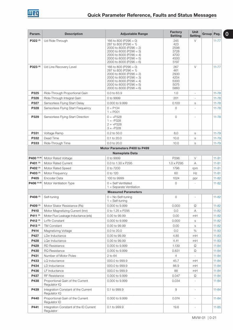
P000 Access Parameter 0 to 999 0 - 11-1
Read Only Parameters P001 to P099
P001 Speed Reference P133 to P134 - rpm
02
11-2
P002 Motor Speed 0 to P134 - rpm 11-2
P003 Motor Current 0 to 3705 A - A 11-2
P004 DC Link Voltage 0 to 8000 - V 11-2
P005 Motor Frequency 0.0 to 300.0 - Hz 11-2
P006 Inverter Status 0 to 28 - - 11-2
P007 Motor Voltage 0 to 8000 - V 11-4
P009 Motor Torque 0.0 to 250.0 - % 11-4
P010 Output Power 0 to 9999 - kW 11-5
P011 Current Inverter 0 to 2600 - A 11-5
P012 Digital Inputs Status DI1 to DI10(MVC4 and optional board)
A = ActiveI = Inactive
- - 11-5
P013 Digital Outputs Status DO1, DO2 and Relays RL1, RL2, RL3, RL4 and RL5 (MVC4 and optional board)
A = ActiveI = Inactive
- - 11-6
P014 Last Fault 0 to 255 - - 11-6
P015 Second Fault 0 to 255 - - 11-6
P016 Third Fault 0 to 255 - - 11-6
P017 Fourth Fault 0 to 255 - - 11-6
P018 Analog Input AI1’ (Unipolar, Board MVC4) 0.0 to 100.0 - % 11-6
P019 Analog Input AI2’ (Bipolar, Board MVC4) -100.0 to +100.0 - % 11-6
P020 Analog Input AI3’ (Board EBB) -100.0 to +100.0 - % 11-6
P021 Analog Input AI4’ (Board EBA) -100.0 to +100.0 - % 11-6
P022 MVC3 Board Temperature 0 to 100 - ºC 11-6
P023 MVC4 Software Version XX.X - - 11-6
P024 A/D Conversion Value of AI4 -32768 to +32767 - - 11-6
P025 A/D Conversion Value of Iv 0 to 4095 - - 11-7
P026 A/D Conversion Value of Iw 0 to 4095 - - 11-7
P027 A/D Conversion Value of Iu 0 to 4095 - - 11-7
P028 Input AI5 ’ (Isolated Unipolar, board MVC4) 0.0 to 100.0 - % 11-7
P029 Trace Function Status 0 = Inactive1 = Waiting for Trigger2 = Trigger Occurred3 = Trace Completed
0 - 11-7
P030 Temperature Register CH 1 0 to 240 - ºC 11-8
P031 Temperature Register CH 2 0 to 240 - ºC 11-8
P032 Temperature Register CH 3 0 to 240 - ºC 11-8
P033 Temperature Register CH 4 0 to 240 - ºC 11-8
P034 Temperature Register CH 5 0 to 240 - ºC 11-8
P035 Temperature Register CH 6 0 to 240 - ºC 11-8
P036 Temperature Register CH 7 0 to 240 - ºC 11-8
P037 Temperature Register CH 8 0 to 240 - ºC 11-8
P040 PID Process Variable 0 to P528 - % 11-8

Quick Parameter Reference, Faults and Status Messages
0-2 | MVW-01
0Param. Description Adjustable Range Factory
SettingUnit
Setting Group Pag.
P041 Active Redundant Ventilation Set 0 = Set A1 = Set B2 = Set A xBx3 = Set B xAx4 = Set A xABx5 = Set B xABx6 = Automatic Test A7 = Automatic Test B
0 -
02
11-9
P042 Energized Hours Counter 0 to 65530 - h 11-9
P043 Enabled Hours Counter 0 to 6553 - h 11-9
P044 MWh Counter 0 to 11930 - MWh 11-9
P045 HMI Software Version XX.X - - 11-9
P046 Junction Temperature -20.0 to +200.0 - °C 11-9
P047 Temperature Phase UAp -20.0 to 200.0 - ºC 11-10
P048 Temperature Phase VAp -20.0 to 200.0 - ºC 11-10
P049 Temperature Phase WAp -20.0 to 200.0 - ºC 11-10
P050 BR. F. p Temperature -20.0 to 200.0 - ºC 11-10
P051 1p Rectifier Temperature -20.0 to 200.0 - ºC 11-10
P052 DC Link Negative Voltage 0 to 8000 - V 11-10
P053 DC Link Positive Voltage 0 to 8000 - V 11-10
P055 U Phase Temperature -20.0 to +200.0 - ºC 11-10
P056 V Phase Temperature -20.0 to +200.0 - ºC 11-10
P057 W Phase Temperature -20.0 to +200.0 - ºC 11-10
P058 Temperature Arm of the Braking Circuit -20.0 to +200.0 - ºC 11-11
P059 Rectifier Temperature -20.0 to +200.0 - ºC 11-11
P060 Fifth Fault 0 to 255 - - 11-11
P061 Sixth Fault 0 to 255 - - 11-11
P062 Seventh Fault 0 to 255 - - 11-11
P063 Eighth Fault 0 to 255 - - 11-11
P064 Ninth Fault 0 to 255 - - 11-11
P065 Tenth Fault 0 to 255 - - 11-11
P066 MVC3 Software Version XX.X - - 11-11
P067 Error Log 1 to 100 - - 11-11
P070 MVC3 DIs Status A = ActiveI = Inactive
- - 11-12
P071 MVC3 DOs Status A = ActiveI = Inactive
- - 11-12
P072 Vab Input Voltage -8000 to +8000 - V 11-12
P073 Vcb Input Voltage -8000 to +8000 - V 11-12
P074 Voltage Modulus of Input Transformer Secondary
0 to 3750 - V 11-12
P075 Medium Point to Ground Voltage 0.0 to 100.0 - % 11-12
P076 Overload I x t 0.0 to 150.0 - % 11-12
P077 Field Current 0 to 999.9 - A 11-12
P078 Brushless Field Voltage 0 to 9999 - V 11-12
P079 Position of the Motor Shaft 0 to 360.0º - - 11-12
P080 Date (dd/mm/yy) - d 11-13
P081 Hour Format 24 h - s 11-13
P082 Temperature Phase UB -20.0 to 200.0 - ºC 11-14
P083 Temperature Phase VB -20.0 to 200.0 - ºC 11-14
P084 Temperature Phase WB -20.0 to 200.0 - ºC 11-14
P085 Temperature Phase UBp -20.0 to 200.0 - ºC 11-14
P086 Temperature Phase VBp -20.0 to 200.0 - ºC 11-14
P087 Temperature Phase WBp -20.0 to 200.0 - ºC 11-14
P088 Temperature Rectifier 2 -20.0 to 200.0 - ºC 11-14
P089 Temperature Rectifier 3 -20.0 to 200.0 - ºC 11-14
P092 Voltage Negative DC Link of Phase V 0 to 8000 - V 11-15
P093 Voltage Positive DC Link of Phase V 0 to 8000 - V 11-15

Quick Parameter Reference, Faults and Status Messages
MVW-01 | 0-3
0Param. Description Adjustable Range Factory
SettingUnit
Setting Group Pag.
P094 Voltage Negative DC Link of Phase W 0 to 8000 - V02
11-15
P095 Voltage Positive DC Link of Phase W 0 to 8000 - V 11-15
Parameters of Regulation P100 to P199
Ramps
P100 Acceleration Time 0.0 to 999.0 100.0 s
20
11-16
P101 Deceleration Time 0.0 to 999.0 180.0 s 11-16
P102 Acceleration Time 2nd Ramp 0.0 to 999.0 100.0 s 11-16
P103 Deceleration Time 2nd Ramp 0.0 to 999.0 180.0 s 11-16
P104 S Ramp 0.0 to 100.0 0.0 % 11-16
P119 Reactive Power reference of the PowerFactor Control
-99.99 to 99.99 - % 11-17
Speed References
P120 Speed Reference Backup 0 = Inactive1 = Active
1 - 11-17
P121 Keypad Reference P133 to P134 90 rpm 11-17
P122 (2) JOG or JOG+ Speed Reference 0 to P134 150 rpm 11-17
P123 (2) JOG- Speed Reference 0 to P134 150 rpm 11-17
P124 (2) Multispeed Reference 1 P133 to P134 90 rpm
35
11-18
P125 (2) Multispeed Reference 2 P133 to P134 300 rpm 11-18
P126 (2) Multispeed Reference 3 P133 to P134 600 rpm 11-18
P127 (2) Multispeed Reference 4 P133 to P134 900 rpm 11-18
P128 (2) Multispeed Reference 5 P133 to P134 1200 rpm 11-18
P129 (2) Multispeed Reference 6 P133 to P134 1500 rpm 11-18
P130 (2) Multispeed Reference 7 P133 to P134 1800 rpm 11-18
P131 (2) Multispeed Reference 8 P133 to P134 1650 rpm 11-18
Speed Limits
P132 Over Speed Level 0 to 100 10 % 11-19
P133 (2) Minimum Speed Reference 0 to (P134 - 1) 90 rpm 11-20
P134 (2) Maximum Speed Reference (P133 + 1) to (3.4 x P402) 1800 rpm 11-20
Control V/F
P136 Manual Torque Boost (I x R) 0 to 100 0 - 11-21
P137 Automatic Torque Boost 0.000 to 1.000 0.000 - 11-22
P138 (2) Slip Compensation -10.00 to +10.00 0.00 % 11-23
P139 Output Current Filter 0.0 to 16.0 0.2 s 11-24
Redundant Ventilation
P140 Redundant Ventilation Selection 0 = Inactive1 = Set A2 = Set B3 = Alternating A4 = Alternating B
0 - 11-25
P141 Time Interval Between Set Alternating 1 to 9999 720 h 11-25
Control V/F Adjustable
P142 (1) Maximum Output Voltage 0.0 to 100.0 100.0 % 11-26
P143 (1) Intermediate Output 0.0 to 100.0 50.0 % 11-26
P144 (1) Output Voltage in 3 Hz 0.0 to 100.0 8.0 % 11-26
P145 (1) (2) Field Weakening Speed P133 (>90) to P134 1800 rpm 11-26
P146 (1) (2) Intermediate Speed 90 to P145 900 rpm 11-26
DC Link Voltage Regulation
P150 (1) DC Link Voltage Regulation Mode 0 to 2 2 - 11-27
P151 (4) DC Link Voltage Regulation Level 325 to 400 (P296 = 0 = 220 V)564 to 800 (P296 = 1 = 380 V)3541 to 4064 (P296 = 2 = 2300 V)5080 to 5831 (P296 = 3 = 3300 V)6404 to 7350 (P296 = 4 = 4160 V)5200 to 6500 (P296 = 5 = 5872 V)7081 to 8127 (P296 = 6 = 4600 V)
375 (P296 = 0)618 (P296 = 1)
3571 (P296 = 2)5123 (P296 = 3)6428 (P296 = 4)6000 (P296 = 5)7107 (P296 = 6)
V 11-28
P152 Proportional Gain 0.00 to 9.99 0.00 - 11-30
Quick Parameter Reference, Faults and Status Messages
0-4 | MVW-01
0 Param. Description Adjustable Range FactorySetting
UnitSetting Group Pag.
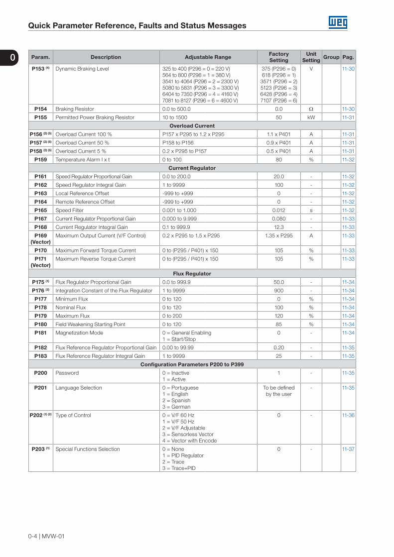
P153 (4) Dynamic Braking Level 325 to 400 (P296 = 0 = 220 V)564 to 800 (P296 = 1 = 380 V)3541 to 4064 (P296 = 2 = 2300 V)5080 to 5831 (P296 = 3 = 3300 V)6404 to 7350 (P296 = 4 = 4160 V)7081 to 8127 (P296 = 6 = 4600 V)
375 (P296 = 0)618 (P296 = 1)
3571 (P296 = 2)5123 (P296 = 3)6428 (P296 = 4)7107 (P296 = 6)
V 11-30
P154 Braking Resistor 0.0 to 500.0 0.0 W 11-30
P155 Permitted Power Braking Resistor 10 to 1500 50 kW 11-31
Overload Current
P156 (2) (5) Overload Current 100 % P157 x P295 to 1.2 x P295 1.1 x P401 A 11-31
P157 (2) (5) Overload Current 50 % P158 to P156 0.9 x P401 A 11-31
P158 (2) (5) Overload Current 5 % 0.2 x P295 to P157 0.5 x P401 A 11-31
P159 Temperature Alarm I x t 0 to 100 80 % 11-32
Current Regulator
P161 Speed Regulator Proportional Gain 0.0 to 200.0 20.0 - 11-32
P162 Speed Regulator Integral Gain 1 to 9999 100 - 11-32
P163 Local Reference Offset -999 to +999 0 - 11-32
P164 Remote Reference Offset -999 to +999 0 - 11-32
P165 Speed Filter 0.001 to 1.000 0.012 s 11-32
P167 Current Regulator Proportional Gain 0.000 to 9.999 0.080 - 11-33
P168 Current Regulator Integral Gain 0.1 to 999.9 12.3 - 11-33
P169 (Vector)
Maximum Output Current (V/F Control) 0.2 x P295 to 1.5 x P295 1.35 x P295 A 11-33
P170 Maximum Forward Torque Current 0 to (P295 / P401) x 150 105 % 11-33
P171 (Vector)
Maximum Reverse Torque Current 0 to (P295 / P401) x 150 105 % 11-33
Flux Regulator
P175 (1) Flux Regulator Proportional Gain 0.0 to 999.9 50.0 - 11-34
P176 (3) Integration Constant of the Flux Regulator 1 to 9999 900 - 11-34
P177 Minimum Flux 0 to 120 0 % 11-34
P178 Nominal Flux 0 to 120 100 % 11-34
P179 Maximum Flux 0 to 200 120 % 11-34
P180 Field Weakening Starting Point 0 to 120 85 % 11-34
P181 Magnetization Mode 0 = General Enabling1 = Start/Stop
0 - 11-34
P182 Flux Reference Regulator Proportional Gain 0.00 to 99.99 0.20 - 11-35
P183 Flux Reference Regulator Integral Gain 1 to 9999 25 - 11-35
Configuration Parameters P200 to P399
P200 Password 0 = Inactive1 = Active
1 - 11-35
P201 Language Selection 0 = Portuguese1 = English2 = Spanish3 = German
To be definedby the user
- 11-35
P202 (1) (2) Type of Control 0 = V/F 60 Hz1 = V/F 50 Hz2 = V/F Adjustable3 = Sensorless Vector4 = Vector with Encode
0 - 11-36
P203 (1) Special Functions Selection 0 = None1 = PID Regulator2 = Trace3 = Trace+PID
0 - 11-37
Quick Parameter Reference, Faults and Status Messages
MVW-01 | 0-5
0Param. Description Adjustable Range FactorySetting
UnitSetting Group Pag.
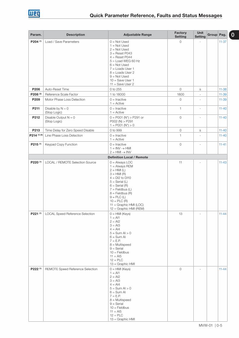
P204 (1) Load / Save Parameters 0 = Not Used1 = Not Used2 = Not Used3 = Reset P0434 = Reset P0445 = Load WEG 60 Hz6 = Not Used7 = Loads User 18 = Loads User 29 = Not Used10 = Save User 111 = Save User 2
0 - 11-37
P206 Auto-Reset Time 0 to 255 0 s 11-38
P208 (2) Reference Scale Factor 1 to 18000 1800 - 11-39
P209 Motor Phase Loss Detection 0 = Inactive1 = Active
0 - 11-39
P211 Disable by N = 0(Stop Logic)
0 = Inactive1 = Active
1 - 11-40
P212 Disable Output N = 0(Stop Logic)
0 = P001 (N*) > P291 orP002 (N) > P2911 = P001 (N*) > 0
0 - 11-40
P213 Time Delay for Zero Speed Disable 0 to 999 0 s 11-40
P214 (1) (6) Line Phase Loss Detection 0 = Inactive1 = Active
1 - 11-40
P215 (1) Keypad Copy Function 0 = Inactive1 = INV → HMI2 = HMI → INV
0 - 11-41
Definition Local / Remote
P220 (1) LOCAL / REMOTE Selection Source 0 = Always LOC1 = Always REM2 = HMI (L)3 = HMI (R)4 = DI2 to DI105 = Serial (L)6 = Serial (R)7 = Fieldbus (L)8 = Fieldbus (R)9 = PLC (L)10 = PLC (R)11 = Graphic HMI (LOC)12 = Graphic HMI (REM)
11 - 11-43
P221 (1) LOCAL Speed Reference Selection 0 = HMI (Keys)1 = AI12 = AI23 = AI34 = AI45 = Sum AI > 06 = Sum AI7 = E.P.8 = Multispeed9 = Serial10 = Fieldbus11 = AI512 = PLC13 = Graphic HMI
13 - 11-44
P222 (1) REMOTE Speed Reference Selection 0 = HMI (Keys)1 = AI12 = AI23 = AI34 = AI45 = Sum AI > 06 = Sum AI7 = E.P.8 = Multispeed9 = Serial10 = Fieldbus11 = AI512 = PLC13 = Graphic HMI
0 - 11-44
Quick Parameter Reference, Faults and Status Messages
0-6 | MVW-01
0 Param. Description Adjustable Range FactorySetting
UnitSetting Group Pag.
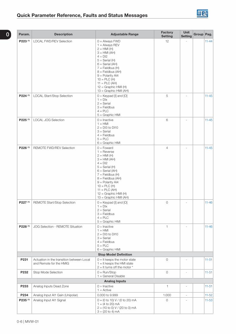
P223 (1) LOCAL FWD/REV Selection 0 = Always FWD1 = Always REV2 = HMI (H)3 = HMI (AH)4 = DI25 = Serial (H)6 = Serial (AH)7 = Fieldbus (H)8 = Fieldbus (AH)9 = Polarity AI410 = PLC (H)11 = PLC (AH)12 = Graphic HMI (H)13 = Graphic HMI (AH)
12 - 11-44
P224 (1) LOCAL Start/Stop Selection 0 = Keypad [I] and [O]1 = DIx2 = Serial3 = Fieldbus4 = PLC5 = Graphic HMI
5 - 11-45
P225 (1) LOCAL JOG Selection 0 = Inactive1 = HMI2 = DI3 to DI103 = Serial4 = Fieldbus5 = PLC6 = Graphic HMI
6 - 11-45
P226 (1) REMOTE FWD/REV Selection 0 = Foward1 = Reverse2 = HMI (H)3 = HMI (AH)4 = DI25 = Serial (H)6 = Serial (AH)7 = Fieldbus (H)8 = Fieldbus (AH)9 = Polarity AI410 = PLC (H)11 = PLC (AH)12 = Graphic HMI (H)13 = Graphic HMI (AH)
4 - 11-45
P227 (1) REMOTE Start/Stop Selection 0 = Keypad [I] and [O]1 = DIx2 = Serial3 = Fieldbus4 = PLC5 = Graphic HMI
0 - 11-46
P228 (1) JOG Selection - REMOTE Situation 0 = Inactive1 = HMI2 = DI3 to DI103 = Serial4 = Fieldbus5 = PLC6 = Graphic HMI
1 - 11-46
Stop Model Definition
P231 Actuation in the transition between Local and Remote for the HMIG
0 = It keeps the motor state 1 = It keeps the HMI state2 = It turns off the motor *
0 - 11-51
P232 Stop Mode Selection 0 = Run/Stop1 = General Disable
0 - 11-51
Analog Inputs
P233 Analog Inputs Dead Zone 0 = Inactive1 = Active
1 - 11-51
P234 Analog Input AI1 Gain (Unipolar) 0.000 to 9.999 1.000 - 11-52
P235 (1) Analog Input AI1 Signal 0 = (0 to 10) V / (0 to 20) mA1 = (4 to 20) mA2 = (10 to 0) V / (20 to 0) mA3 = (20 to 4) mA
0 - 11-53
Quick Parameter Reference, Faults and Status Messages
MVW-01 | 0-7
0Param. Description Adjustable Range FactorySetting
UnitSetting Group Pag.
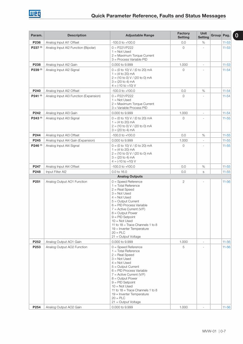
P236 Analog Input AI1 Offset -100.0 to +100.0 0.0 % 11-53
P237 (1) Analog Input AI2 Function (Bipolar) 0 = P221/P2221 = Not Used2 = Maximum Torque Current3 = Process Variable PID
0 - 11-53
P238 Analog Input AI2 Gain 0.000 to 9.999 1.000 - 11-53
P239 (1) Analog Input AI2 Signal 0 = (0 to 10) V / (0 to 20) mA1 = (4 to 20) mA2 = (10 to 0) V / (20 to 0) mA3 = (20 to 4) mA4 = (-10 to +10) V
0 - 11-54
P240 Analog Input AI2 Offset -100.0 to +100.0 0.0 % 11-54
P241 (1) Analog Input AI3 Function (Expansion) 0 = P221/P2221 = Not Used2 = Maximum Torque Current3 = Variable Process PID
0 - 11-54
P242 Analog Input AI3 Gain 0.000 to 9.999 1.000 - 11-54
P243 (1) Analog Input AI3 Signal 0 = (0 to 10) V / (0 to 20) mA1 = (4 to 20) mA2 = (10 to 0) V / (20 to 0) mA3 = (20 to 4) mA
0 - 11-55
P244 Analog Input AI3 Offset -100.0 to +100.0 0.0 % 11-55
P245 Analog Input AI4 Gain (Expansion) 0.000 to 9.999 1.000 - 11-55
P246 (1) Analog Input AI4 Signal 0 = (0 to 10) V / (0 to 20) mA1 = (4 to 20) mA2 = (10 to 0) V / (20 to 0) mA3 = (20 to 4) mA4 = (-10 to +10) V
0 - 11-55
P247 Analog Input AI4 Offset -100.0 to +100.0 0.0 % 11-55
P248 Input Filter AI2 0.0 to 16.0 0.0 s 11-55Analog Outputs
P251 Analog Output AO1 Function 0 = Speed Reference1 = Total Reference2 = Real Speed3 = Not Used4 = Not Used5 = Output Current6 = PID Process Variable7 = Active Current (V/F)8 = Output Power9 = PID Setpoint10 = Not Used11 to 18 = Trace Channels 1 to 819 = Inverter Temperature20 = PLC21 = Output Voltage
2 - 11-56
P252 Analog Output AO1 Gain 0.000 to 9.999 1.000 - 11-56
P253 Analog Output AO2 Function 0 = Speed Reference1 = Total Reference2 = Real Speed3 = Not Used4 = Not Used5 = Output Current6 = PID Process Variable7 = Active Current (V/F)8 = Output Power9 = PID Setpoint10 = Not Used11 to 18 = Trace Channels 1 to 819 = Inverter Temperature20 = PLC21 = Output Voltage
5 - 11-56
P254 Analog Output AO2 Gain 0.000 to 9.999 1.000 - 11-56
Quick Parameter Reference, Faults and Status Messages
0-8 | MVW-01
0 Param. Description Adjustable Range FactorySetting
UnitSetting Group Pag.
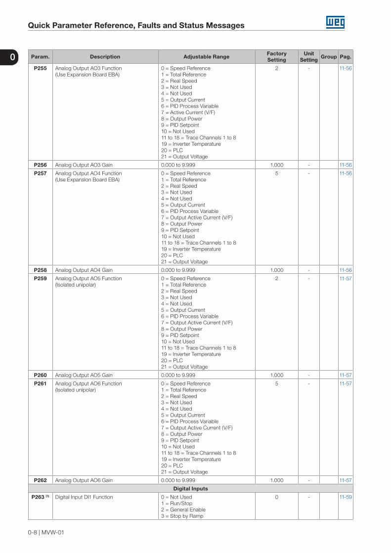
P255 Analog Output AO3 Function(Use Expansion Board EBA)
0 = Speed Reference1 = Total Reference2 = Real Speed3 = Not Used4 = Not Used5 = Output Current6 = PID Process Variable7 = Active Current (V/F)8 = Output Power9 = PID Setpoint10 = Not Used11 to 18 = Trace Channels 1 to 819 = Inverter Temperature20 = PLC21 = Output Voltage
2 - 11-56
P256 Analog Output AO3 Gain 0.000 to 9.999 1.000 - 11-56
P257 Analog Output AO4 Function(Use Expansion Board EBA)
0 = Speed Reference1 = Total Reference2 = Real Speed3 = Not Used4 = Not Used5 = Output Current6 = PID Process Variable7 = Output Active Current (V/F)8 = Output Power9 = PID Setpoint10 = Not Used11 to 18 = Trace Channels 1 to 819 = Inverter Temperature20 = PLC21 = Output Voltage
5 - 11-56
P258 Analog Output AO4 Gain 0.000 to 9.999 1.000 - 11-56
P259 Analog Output AO5 Function(Isolated unipolar)
0 = Speed Reference1 = Total Reference2 = Real Speed3 = Not Used4 = Not Used5 = Output Current6 = PID Process Variable7 = Output Active Current (V/F)8 = Output Power9 = PID Setpoint10 = Not Used11 to 18 = Trace Channels 1 to 819 = Inverter Temperature20 = PLC21 = Output Voltage
2 - 11-57
P260 Analog Output AO5 Gain 0.000 to 9.999 1.000 - 11-57
P261 Analog Output AO6 Function(Isolated unipolar)
0 = Speed Reference1 = Total Reference2 = Real Speed3 = Not Used4 = Not Used5 = Output Current6 = PID Process Variable7 = Output Active Current (V/F)8 = Output Power9 = PID Setpoint10 = Not Used11 to 18 = Trace Channels 1 to 819 = Inverter Temperature20 = PLC21 = Output Voltage
5 - 11-57
P262 Analog Output AO6 Gain 0.000 to 9.999 1.000 - 11-57
Digital Inputs
P263 (1) Digital Input DI1 Function 0 = Not Used1 = Run/Stop2 = General Enable3 = Stop by Ramp
0 - 11-59
Quick Parameter Reference, Faults and Status Messages
MVW-01 | 0-9
0Param. Description Adjustable Range FactorySetting
UnitSetting Group Pag.
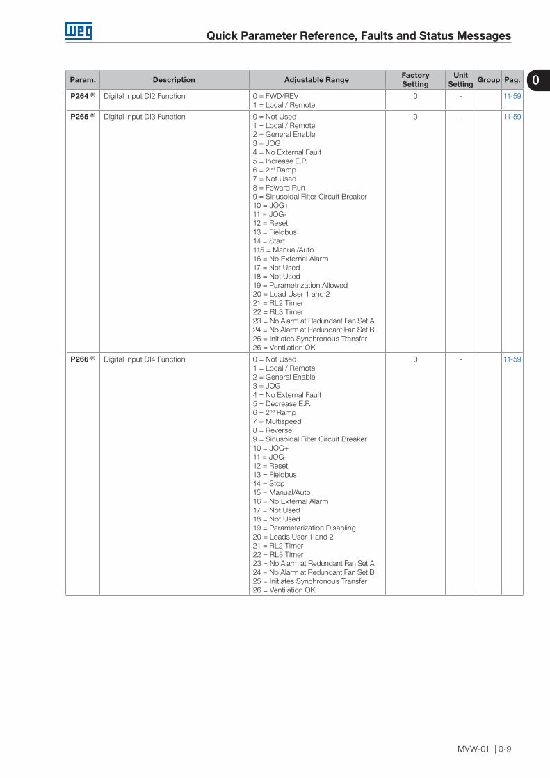
P264 (1) Digital Input DI2 Function 0 = FWD/REV1 = Local / Remote
0 - 11-59
P265 (1) Digital Input DI3 Function 0 = Not Used1 = Local / Remote2 = General Enable3 = JOG4 = No External Fault5 = Increase E.P.6 = 2nd Ramp7 = Not Used8 = Foward Run9 = Sinusoidal Filter Circuit Breaker10 = JOG+11 = JOG-12 = Reset13 = Fieldbus14 = Start115 = Manual/Auto16 = No External Alarm17 = Not Used18 = Not Used19 = Parametrization Allowed20 = Load User 1 and 221 = RL2 Timer22 = RL3 Timer23 = No Alarm at Redundant Fan Set A24 = No Alarm at Redundant Fan Set B25 = Initiates Synchronous Transfer26 = Ventilation OK
0 - 11-59
P266 (1) Digital Input DI4 Function 0 = Not Used1 = Local / Remote2 = General Enable3 = JOG4 = No External Fault5 = Decrease E.P.6 = 2nd Ramp7 = Multispeed8 = Reverse9 = Sinusoidal Filter Circuit Breaker10 = JOG+11 = JOG-12 = Reset13 = Fieldbus14 = Stop15 = Manual/Auto16 = No External Alarm17 = Not Used18 = Not Used19 = Parameterization Disabling20 = Loads User 1 and 221 = RL2 Timer22 = RL3 Timer23 = No Alarm at Redundant Fan Set A24 = No Alarm at Redundant Fan Set B25 = Initiates Synchronous Transfer26 = Ventilation OK
0 - 11-59
Quick Parameter Reference, Faults and Status Messages
0-10 | MVW-01
0 Param. Description Adjustable Range FactorySetting
UnitSetting Group Pag.
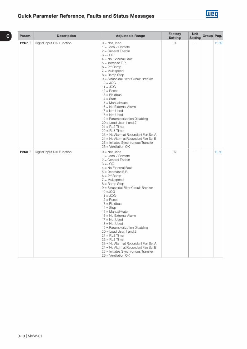
P267 (1) Digital Input DI5 Function 0 = Not Used1 = Local / Remote2 = General Enable3 = JOG4 = No External Fault5 = Increase E.P.6 = 2nd Ramp7 = Multispeed8 = Ramp Stop9 = Sinusoidal Filter Circuit Breaker10 = JOG+11 = JOG-12 = Reset13 = Fieldbus14 = Start15 = Manual/Auto16 = No External Alarm17 = Not Used18 = Not Used19 = Parameterization Disabling20 = Load User 1 and 221 = RL2 Timer22 = RL3 Timer23 = No Alarm at Redundant Fan Set A24 = No Alarm at Redundant Fan Set B25 = Initiates Synchronous Transfer26 = Ventilation OK
3 - 11-59
P268 (1) Digital Input DI6 Function 0 = Not Used1 = Local / Remote2 = General Enable3 = JOG4 = No External Fault5 = Decrease E.P.6 = 2nd Ramp7 = Multispeed8 = Ramp Stop9 = Sinusoidal Filter Circuit Breaker10 =JOG+11 = JOG-12 = Reset13 = Fieldbus14 = Stop15 = Manual/Auto16 = No External Alarm17 = Not Used18 = Not Used19 = Parameterization Disabling20 = Load User 1 and 221 = RL2 Timer22 = RL3 Timer23 = No Alarm at Redundant Fan Set A24 = No Alarm at Redundant Fan Set B25 = Initiates Synchronous Transfer26 = Ventilation OK
6 - 11-59
Quick Parameter Reference, Faults and Status Messages
MVW-01 | 0-11
0Param. Description Adjustable Range FactorySetting
UnitSetting Group Pag.
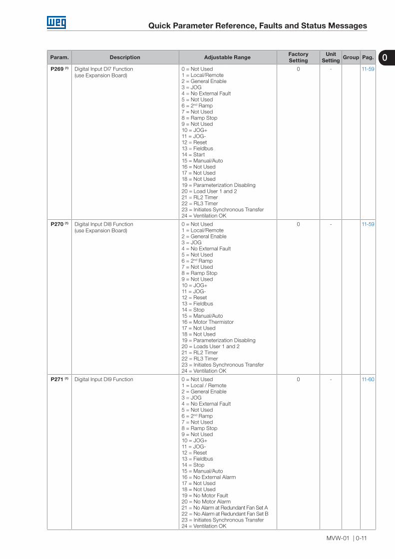
P269 (1) Digital Input DI7 Function(use Expansion Board)
0 = Not Used1 = Local/Remote2 = General Enable3 = JOG4 = No External Fault5 = Not Used6 = 2nd Ramp7 = Not Used8 = Ramp Stop9 = Not Used10 = JOG+11 = JOG-12 = Reset13 = Fieldbus14 = Start15 = Manual/Auto16 = Not Used17 = Not Used18 = Not Used19 = Parameterization Disabling20 = Load User 1 and 221 = RL2 Timer22 = RL3 Timer23 = Initiates Synchronous Transfer24 = Ventilation OK
0 - 11-59
P270 (1) Digital Input DI8 Function(use Expansion Board)
0 = Not Used1 = Local/Remote2 = General Enable3 = JOG4 = No External Fault5 = Not Used6 = 2nd Ramp7 = Not Used8 = Ramp Stop9 = Not Used10 = JOG+11 = JOG-12 = Reset13 = Fieldbus14 = Stop15 = Manual/Auto16 = Motor Thermistor17 = Not Used18 = Not Used19 = Parameterization Disabling20 = Loads User 1 and 221 = RL2 Timer22 = RL3 Timer23 = Initiates Synchronous Transfer24 = Ventilation OK
0 - 11-59
P271 (1) Digital Input DI9 Function 0 = Not Used1 = Local / Remote2 = General Enable3 = JOG4 = No External Fault5 = Not Used6 = 2nd Ramp7 = Not Used8 = Ramp Stop9 = Not Used10 = JOG+11 = JOG-12 = Reset13 = Fieldbus14 = Stop15 = Manual/Auto16 = No External Alarm17 = Not Used18 = Not Used19 = No Motor Fault20 = No Motor Alarm21 = No Alarm at Redundant Fan Set A22 = No Alarm at Redundant Fan Set B23 = Initiates Synchronous Transfer24 = Ventilation OK
0 - 11-60

Quick Parameter Reference, Faults and Status Messages
0-12 | MVW-01
0 Param. Description Adjustable Range FactorySetting
UnitSetting Group Pag.
P272 (1) Digital Input DI10 Function 0 = Not Used1 = Local/Remote2 = General Enable3 = JOG4 = No External Fault5 = Not Used6 = 2nd Ramp7 = Not Used8 = Ramp Stop9 = Not Used10 = JOG+11 = JOG-12 = Reset13 = Fieldbus14 = Stop15 = Manual/Auto16 = No External Alarm17 = Not Used18 = Not Used19 = No Motor Fault20 = No Motor Alarm21 = No Alarm at Redundant Fan Set A22 = No Alarm at Redundant Fan Set B23 = Initiates Synchronous Transfer24 = Ventilation OK
0 - 11-60
Digital Outputs
P275 (1) Digital Output DO1 Function(use Expansion Board)
0 = Not Used1 = N* > Nx2 = N > Nx3 = N < Ny4 = N = N*5 = N = 06 = Is > Ix7 = Is < Ix8 = Not Used9 = Not Used10 = Remote11 = Run12 = Ready13 = No Fault14 = No E71 + E7015 = No E22 + E21 + E0616 = No E6217 = No E7218 = (4 to 20) mA OK19 = Fieldbus20 = Forward21 = Process Variable > VPx22 = Process Variable < VPy23 = Not Used24 = Pre-charge OK25 = With Fault26 = N > Nx and Nt > Nx27 = No Fault, with Delay28 = No Alarm29 = Not Used30 = Redundant Ventilation Selection31 = Not Used32 = Circuit Break ON (Input Circuit Breaker ON)33 = Transfer OK34 = Synchronism OK35 = Serial36 = Safety Stop37 = Sinusoidal Filter Circuit Breaker38 = Normal/Slave
0 - 11-66
Quick Parameter Reference, Faults and Status Messages
MVW-01 | 0-13
0Param. Description Adjustable Range FactorySetting
UnitSetting Group Pag.
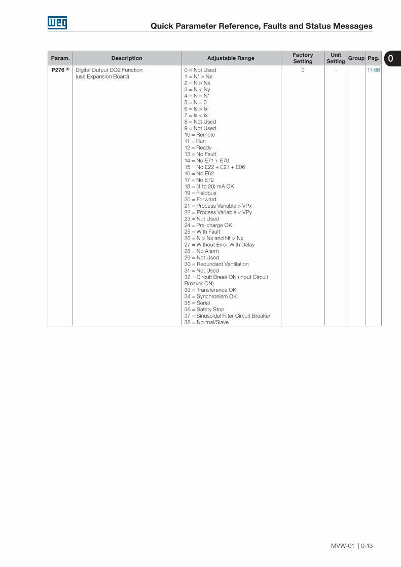
P276 (1) Digital Output DO2 Function(use Expansion Board)
0 = Not Used1 = N* > Nx2 = N > Nx3 = N < Ny4 = N = N*5 = N = 06 = Is > Ix7 = Is < Ix8 = Not Used9 = Not Used10 = Remote11 = Run12 = Ready13 = No Fault14 = No E71 + E7015 = No E22 + E21 + E0616 = No E6217 = No E7218 = (4 to 20) mA OK19 = Fieldbus20 = Forward21 = Process Variable > VPx22 = Process Variable < VPy23 = Not Used24 = Pre-charge OK25 = With Fault26 = N > Nx and Nt > Nx27 = Without Error With Delay28 = No Alarm29 = Not Used30 = Redundant Ventilation31 = Not Used32 = Circuit Break ON (Input Circuit Breaker ON)33 = Transference OK34 = Synchronism OK35 = Serial36 = Safety Stop37 = Sinusoidal Filter Circuit Breaker38 = Normal/Slave
0 - 11-66

Quick Parameter Reference, Faults and Status Messages
0-14 | MVW-01
0 Param. Description Adjustable Range FactorySetting
UnitSetting Group Pag.
P277 (1) Relay Output RL1 Function 0 = Not Used1 = N* > Nx2 = N > Nx3 = N < Ny4 = N = N*5 = N = 06 = Is > Ix7 = Is < Ix8 = Not Used9 = Not Used10 = Remote11 = Run12 = Ready13 = No Fault14 = No E71 + E7015 = No E22 + E21 + E0616 = No E6217 = No E7218 = (4 to 20) mA OK19 = Fieldbus20 = Forward21 = Process Variable > VPx22 = Process Variable < VPy23 = Not Used24 = Pre-charge OK25 = With Fault26 = N > Nx and Nt > Nx27 = No Fault, with Delay28 = No Alarm29 = Not Used30 = Redundant Ventilation31 = PLC32 = Circuit Break ON (Input Circuit Breaker ON)33 = Transference OK34 = Synchronism OK35 = Serial36 = Safety Stop37 = Sinusoidal Filter Circuit Breaker38 = Normal/Slave
13 - 11-66

Quick Parameter Reference, Faults and Status Messages
MVW-01 | 0-15
0Param. Description Adjustable Range FactorySetting
UnitSetting Group Pag.
P279 (1) Relay Output RL2 Function 0 = Not Used1 = N* > Nx2 = N > Nx3 = N < Ny4 = N = N*5 = N = 06 = Is > Ix7 = Is < Ix8 = Not Used9 = Not Used10 = Remote11 = Run12 = Ready13 = No Fault14 = No E71 + E7015 = No E22 + E21 + E0616 = No E6217 = No E7218 = (4 to 20) mA OK19 = Fieldbus20 = Forward21 = Process Variable > VPx22 = Process Variable < VPy23 = Not Used24 = Pre-charge OK25 = With Fault26 = N > Nx and Nt > Nx27 = Without error with delay28 = No Alarm29 = Timer30 = Redundant Ventilation31 = PLC32 = Circuit Break ON (Input Circuit Breaker ON)33 = Transference OK34 = Synchronism OK35 = Serial36 = Safety Stop37 = Sinusoidal Filter Circuit Breaker38 = Normal/Slave
2 - 11-66
Quick Parameter Reference, Faults and Status Messages
0-16 | MVW-01
0 Param. Description Adjustable Range FactorySetting
UnitSetting Group Pag.
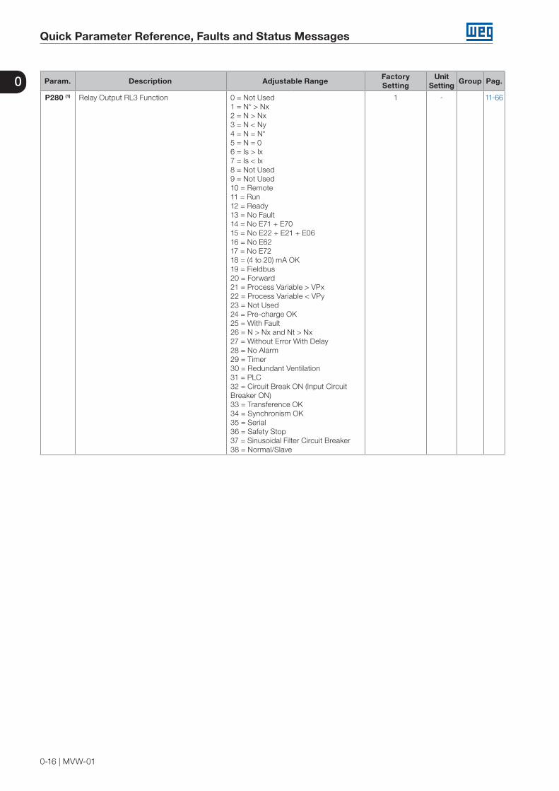
P280 (1) Relay Output RL3 Function 0 = Not Used1 = N* > Nx2 = N > Nx3 = N < Ny4 = N = N*5 = N = 06 = Is > Ix7 = Is < Ix8 = Not Used9 = Not Used10 = Remote11 = Run12 = Ready13 = No Fault14 = No E71 + E7015 = No E22 + E21 + E0616 = No E6217 = No E7218 = (4 to 20) mA OK19 = Fieldbus20 = Forward21 = Process Variable > VPx22 = Process Variable < VPy23 = Not Used24 = Pre-charge OK25 = With Fault26 = N > Nx and Nt > Nx27 = Without Error With Delay28 = No Alarm29 = Timer30 = Redundant Ventilation31 = PLC32 = Circuit Break ON (Input Circuit Breaker ON)33 = Transference OK34 = Synchronism OK35 = Serial36 = Safety Stop37 = Sinusoidal Filter Circuit Breaker38 = Normal/Slave
1 - 11-66
Quick Parameter Reference, Faults and Status Messages
MVW-01 | 0-17
0Param. Description Adjustable Range FactorySetting
UnitSetting Group Pag.
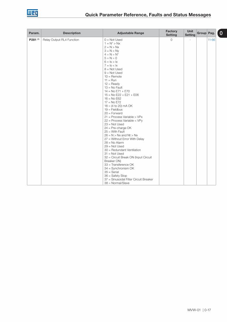
P281 (1) Relay Output RL4 Function 0 = Not Used1 = N* > Nx2 = N > Nx3 = N < Ny4 = N = N*5 = N = 06 = Is > Ix7 = Is < Ix8 = Not Used9 = Not Used10 = Remote11 = Run12 = Ready13 = No Fault14 = No E71 + E7015 = No E22 + E21 + E0616 = No E6217 = No E7218 = (4 to 20) mA OK19 = Fieldbus20 = Forward21 = Process Variable > VPx22 = Process Variable < VPy23 = Not Used24 = Pre-charge OK25 = With Fault26 = N > Nx and Nt > Nx27 = Without Error With Delay28 = No Alarm29 = Not Used30 = Redundant Ventilation31 = Not Used32 = Circuit Break ON (Input Circuit Breaker ON)33 = Transference OK34 = Synchronism OK35 = Serial36 = Safety Stop37 = Sinusoidal Filter Circuit Breaker38 = Normal/Slave
0 - 11-66
Quick Parameter Reference, Faults and Status Messages
0-18 | MVW-01
0 Param. Description Adjustable Range FactorySetting
UnitSetting Group Pag.
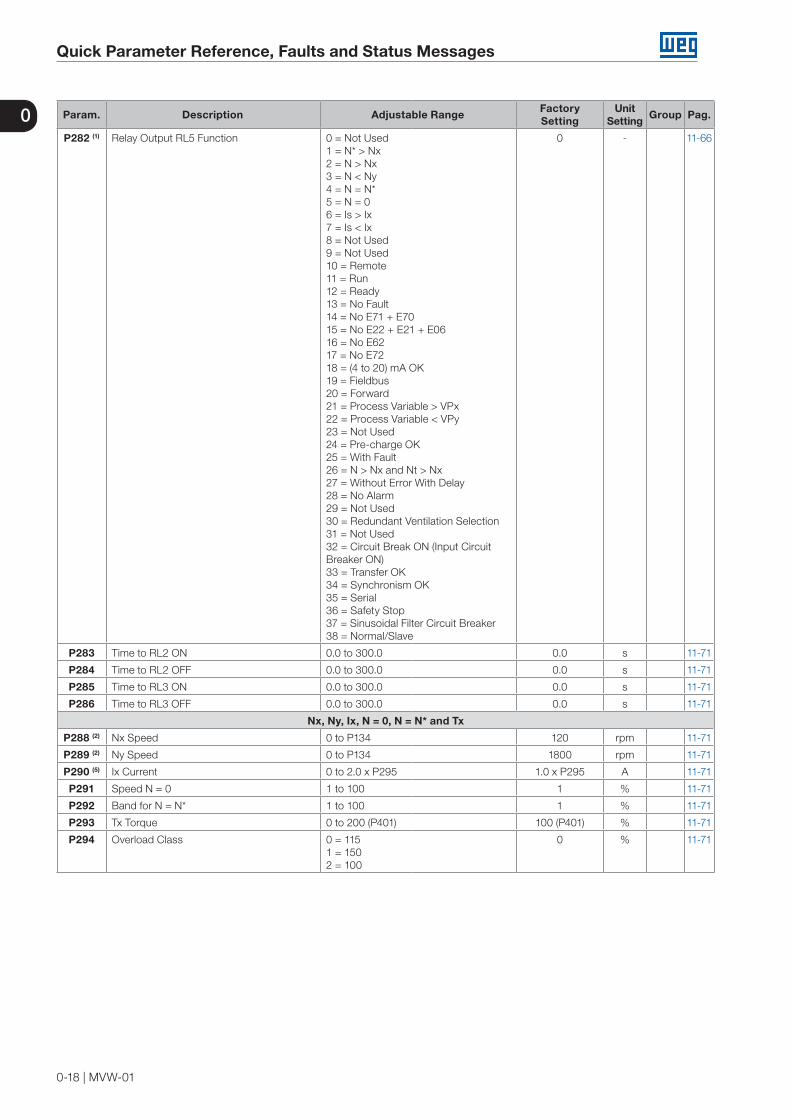
P282 (1) Relay Output RL5 Function 0 = Not Used1 = N* > Nx2 = N > Nx3 = N < Ny4 = N = N*5 = N = 06 = Is > Ix7 = Is < Ix8 = Not Used9 = Not Used10 = Remote11 = Run12 = Ready13 = No Fault14 = No E71 + E7015 = No E22 + E21 + E0616 = No E6217 = No E7218 = (4 to 20) mA OK19 = Fieldbus20 = Forward21 = Process Variable > VPx22 = Process Variable < VPy23 = Not Used24 = Pre-charge OK25 = With Fault26 = N > Nx and Nt > Nx27 = Without Error With Delay28 = No Alarm29 = Not Used30 = Redundant Ventilation Selection31 = Not Used32 = Circuit Break ON (Input Circuit Breaker ON)33 = Transfer OK34 = Synchronism OK35 = Serial36 = Safety Stop37 = Sinusoidal Filter Circuit Breaker38 = Normal/Slave
0 - 11-66
P283 Time to RL2 ON 0.0 to 300.0 0.0 s 11-71
P284 Time to RL2 OFF 0.0 to 300.0 0.0 s 11-71
P285 Time to RL3 ON 0.0 to 300.0 0.0 s 11-71
P286 Time to RL3 OFF 0.0 to 300.0 0.0 s 11-71
Nx, Ny, Ix, N = 0, N = N* and Tx
P288 (2) Nx Speed 0 to P134 120 rpm 11-71
P289 (2) Ny Speed 0 to P134 1800 rpm 11-71
P290 (5) Ix Current 0 to 2.0 x P295 1.0 x P295 A 11-71
P291 Speed N = 0 1 to 100 1 % 11-71
P292 Band for N = N* 1 to 100 1 % 11-71
P293 Tx Torque 0 to 200 (P401) 100 (P401) % 11-71
P294 Overload Class 0 = 1151 = 1502 = 100
0 % 11-71

Quick Parameter Reference, Faults and Status Messages
MVW-01 | 0-19
0Param. Description Adjustable Range FactorySetting
UnitSetting Group Pag.
Inverter Data
P295 (1) Inverter Rated Current G10 = 32 A1 = 53 A2 = 70 A3 = 80 A4 = 85 A5 = 94 A6 = 100 A7 = 110 A8 = 112 A9 = 120 A10 = 130 A11 = 138 A12 = 140 A13 = 150 A14 = 160 A15 = 162 A16 = 165 A17 = 170 A18 = 175 A19 = 186 A20 = 188 A21 = 210 A22 = 235 A23 = 250 A24 = 265 A25 = 280 A26 = 300 A27 = 310 A28 = 357 A29 = 375 A30 = 386 A31 = 450 A32 = 475 A33 = 490 A34 = 500 A35 = 560 A36 = 580 A37 = 1064 A38 = 712 A39 = 880 A40 = 950 A41 = 1178 A42 = 200 A43 = 125 A44 = 536 A45 = 1072 A46 = 1340 A47 = 1424 A48 = 1760 A49 = 1900 A50 = 2356 A51 = 301 A
G270 = 54 A71 = 58 A72 = 67 A73 = 73 A74 = 78 A75 = 86 A76 = 91 A77 = 92 A78 = 96 A79 = 108 A80 = 109 A81 = 113 A82 = 114 A83 = 128 A84 = 131 A85 = 139 A86 = 144 A87 = 151 A88 = 152 A89 = 176 A90 = 177 A91 = 180 A92 = 181 A93 = 204 A94 = 205 A95 = 212 A96 = 216 A97 = 237 A98 = 241 A99 = 251 A100 = 260 A101 = 276 A102 = 283 A103 = 294 A104 = 295 A105 = 322 A106 = 330 A107 = 332 A108 = 348 A109 = 376 A110 = 390 A111 = 405 A112 = 410 A113 = 440 A114 = 458 A115 = 481 A116 = 494 A117 = 517 A118 = 538 A119 = 561 A120 = 565 A121 = 607 A122 = 627 A123 = 631 A124 = 664 A125 = 713 A126 = 740 A127 = 741 A128 = 779 A129 = 816 A130 = 835 A131 = 934 A132 = 941 A133 = 1069 A134 = 1087 A135 = 1234 A136 = 1254 A137 = 1425 A138 = 1482 A139 = 1632 A140 = 1881 A141 = 2138 A142 = 2508 A143 = 2850 A
According to the rated current of
the Inverter
A 11-72
Quick Parameter Reference, Faults and Status Messages
0-20 | MVW-01
0 Param. Description Adjustable Range FactorySetting
UnitSetting Group Pag.
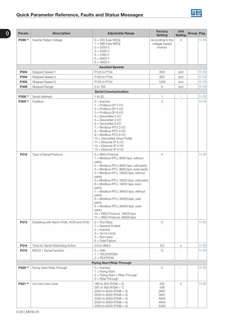
P296 (1) Inverter Rated Voltage 0 = 220 (Use WEG)1 = 380 (Use WEG)2 = 2300 V3 = 3300 V4 = 4160 V5 = 6900 V6 = 4600 V
According to the voltage supply
Inverter
V 11-73
Avoided Speeds
P303 Skipped Speed 1 P133 to P134 600 rpm 11-73
P304 Skipped Speed 2 P133 to P134 900 rpm 11-73
P305 Skipped Speed 3 P133 to P134 1200 rpm 11-73
P306 Skipped Range 0 to 750 0 rpm 11-73
Serial Communication
P308 (1) Serial Address 1 to 30 1 - 11-73
P309 (1) Fieldbus 0 = Inactive1 = Profibus DP 2 I/O2 = Profibus DP 4 I/O3 = Profibus DP 6 I/O4 = DeviceNet 2 I/O5 = DeviceNet 4 I/O6 = DeviceNet 6 I/O7 = Modbus-RTU 2 I/O8 = Modbus-RTU 4 I/O9 = Modbus-RTU 6 I/O10 = DeviceNet Drive Profile11 = Ethernet IP 2 I/O12 = Ethernet IP 4 I/O13 = Ethernet IP 6 I/O
0 - 11-74
P312 Type of Serial Protocol 0 = WEG Protocol1 = Modbus-RTU, 9600 bps, without parity2 = Modbus-RTU, 9600 bps, odd parity3 = Modbus-RTU, 9600 bps, even parity4 = Modbus-RTU, 19200 bps, without parity5 = Modbus-RTU, 19200 bps, odd parity6 = Modbus-RTU, 19200 bps, even parity7 = Modbus-RTU, 38400 bps, without parity8 = Modbus-RTU, 38400 bps, odd parity9 = Modbus-RTU, 38400 bps, even parity10 = WEG Protocol, 19200 bps11 = WEG Protocol, 38400 bps
0 - 11-74
P313 Disabling with Alarm A128, A129 and A130 0 = Run/Stop1 = General Enable2 = Inactive3 = Go to Local4 = Not Used5 = Fatal Failure
0 - 11-75
P314 Time for Serial Watchdog Action 0.0 to 999.0 0.0 s 11-75
P315 MVC3 1 Serial Function 0 = HMI1 = TECSYSTEM2 = PEXTRON
0 - 11-75
Flying Start/Ride-Through
P320 (1) Flying Start/Ride-Through 0 = Inactive1 = Flying Start2 = Flying Start + Ride-Through3 = Ride-Through
0 - 11-75
P321 (4) Ud Line Loss Level 166 to 800 (P296 = 0)287 to 800 (P296 = 1)2000 to 8000 (P296 = 2)2000 to 8000 (P296 = 3)2000 to 8000 (P296 = 4)2000 to 8000 (P296 = 5)2000 to 8000 (P296 = 6)
25243626813847485046445363
V 11-76
Quick Parameter Reference, Faults and Status Messages
MVW-01 | 0-21
0Param. Description Adjustable Range FactorySetting
UnitSetting Group Pag.
P322 (4) Ud Ride-Through 166 to 800 (P296 = 0)287 to 800 (P296 = 1)2000 to 8000 (P296 = 2)2000 to 8000 (P296 = 3)2000 to 8000 (P296 = 4)2000 to 8000 (P296 = 5)2000 to 8000 (P296 = 6)
245423
25983728470045005197
V 11-77
P323 (4) Ud Line Recovery Level 166 to 800 (P296 = 0)287 to 800 (P296 = 1)2000 to 8000 (P296 = 2)2000 to 8000 (P296 = 3)2000 to 8000 (P296 = 4)2000 to 8000 (P296 = 5)2000 to 8000 (P296 = 6)
267461
29304204530050755860
V 11-77
P325 Ride-Through Proportional Gain 0.0 to 63.9 1.0 - 11-78
P326 Ride-Through Integral Gain 0 to 9999 201 - 11-78
P327 Sensorless Flying Start Delay 0.000 to 9.999 0.100 s 11-78
P328 Sensorless Flying Start Frequency 0 = P1341 = P001
0 - 11-78
P329 Sensorless Flying Start Direction 0 = +P3281 = -P3282 = +P3283 = -P328
0 - 11-78
P331 Voltage Ramp 0.2 to 50.0 8,0 s 11-79
P332 Dead Time 0.1 to 20.0 10.0 s 11-79
P333 Ride-Through Time 0.0 to 20.0 10.0 s 11-79
Motor Parameters P400 to P499
Nameplate Data
P400 (1) (4) Motor Rated Voltage 0 to 9999 P296 V 11-81
P401 (1) Motor Rated Current 0.0 to 1.30 x P295 1.0 x P295 A 11-81
P402 (1) Motor Rated Speed 0 to 7200 1796 rpm 11-81
P403 (1) Motor Frequency 0 to 120 60 Hz 11-81
P405 Encoder Data 100 to 9999 1024 ppr 11-82
P406 (1) (2) Motor Ventilation Type 0 = Self Ventilated1 = Separate Ventilation
0 - 11-82
Measured Parameters
P408 (1) Self-tuning 0 = No Self-tuning1 = Self-tuning
0 - 11-82
P409 (1) Motor Stator Resistance (Rs) 0.000 to 9.999 0.000 Ω 11-82
P410 Motor Magnetizing Current (Imr) 0 to 1.25 x P295 0.0 A 11-82
P411 (1) Motor Flux Leakage Inductance (σIs) 0.00 to 99.99 0.00 mH 11-82
P412 (1) Lr/Rr Constant 0.000 to 9.999 0.000 s 11-82
P413 (1) TM Constant 0.00 to 99.99 0.00 s 11-82
P414 Magnetizing Voltage 0.0 to 20.0 0.0 % 11-83
P427 LDσ Inductance 0.00 to 99.99 4.85 mH 11-83
P428 LQσ Inductance 0.00 to 99.99 4.41 mH 11-83
P429 RD Resistance 0.000 to 9.999 1.139 Ω 11-84
P430 RQ Resistance 0.000 to 9.999 0.831 Ω 11-84
P431 Number of Motor Poles 2 to 64 4 - 11-84
P433 LQ Inductance 000.0 to 999.9 45.7 mH 11-84
P434 LD Inductance 000.0 to 999.9 86.9 mH 11-84
P436 LF Inductance 000.0 to 999.9 88 mH 11-84
P437 RF Resistance 0.000 to 9.999 0.047 Ω 11-84
P438 Proportional Gain of the CurrentRegulator IQ
0.000 to 9.999 0.034 - 11-84
P439 Integration Constant of the CurrentRegulator IQ
0.1 to 999.9 9 - 11-84
P440 Proportional Gain of the CurrentRegulator ID
0.000 to 9.999 0.074 - 11-84
P441 Integration Constant of the ID CurrentRegulator
0.1 to 999.9 19.6 - 11-85
Quick Parameter Reference, Faults and Status Messages
0-22 | MVW-01
0 Param. Description Adjustable Range FactorySetting
UnitSetting Group Pag.
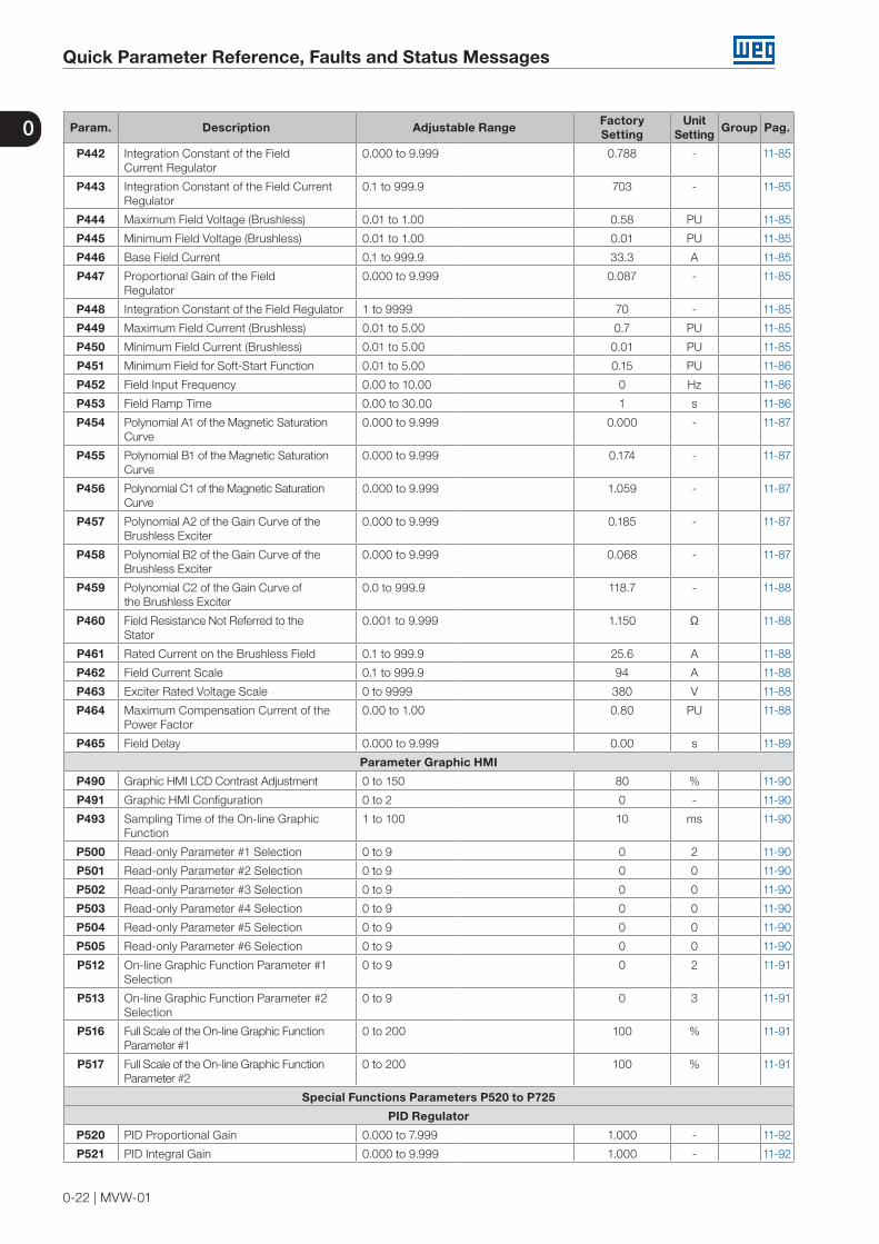
P442 Integration Constant of the FieldCurrent Regulator
0.000 to 9.999 0.788 - 11-85
P443 Integration Constant of the Field CurrentRegulator
0.1 to 999.9 703 - 11-85
P444 Maximum Field Voltage (Brushless) 0.01 to 1.00 0.58 PU 11-85
P445 Minimum Field Voltage (Brushless) 0.01 to 1.00 0.01 PU 11-85
P446 Base Field Current 0.1 to 999.9 33.3 A 11-85
P447 Proportional Gain of the FieldRegulator
0.000 to 9.999 0.087 - 11-85
P448 Integration Constant of the Field Regulator 1 to 9999 70 - 11-85
P449 Maximum Field Current (Brushless) 0.01 to 5.00 0.7 PU 11-85
P450 Minimum Field Current (Brushless) 0.01 to 5.00 0.01 PU 11-85
P451 Minimum Field for Soft-Start Function 0.01 to 5.00 0.15 PU 11-86
P452 Field Input Frequency 0.00 to 10.00 0 Hz 11-86
P453 Field Ramp Time 0.00 to 30.00 1 s 11-86
P454 Polynomial A1 of the Magnetic Saturation Curve
0.000 to 9.999 0.000 - 11-87
P455 Polynomial B1 of the Magnetic Saturation Curve
0.000 to 9.999 0.174 - 11-87
P456 Polynomial C1 of the Magnetic Saturation Curve
0.000 to 9.999 1.059 - 11-87
P457 Polynomial A2 of the Gain Curve of the Brushless Exciter
0.000 to 9.999 0.185 - 11-87
P458 Polynomial B2 of the Gain Curve of the Brushless Exciter
0.000 to 9.999 0.068 - 11-87
P459 Polynomial C2 of the Gain Curve ofthe Brushless Exciter
0.0 to 999.9 118.7 - 11-88
P460 Field Resistance Not Referred to theStator
0.001 to 9.999 1.150 Ω 11-88
P461 Rated Current on the Brushless Field 0.1 to 999.9 25.6 A 11-88
P462 Field Current Scale 0.1 to 999.9 94 A 11-88
P463 Exciter Rated Voltage Scale 0 to 9999 380 V 11-88
P464 Maximum Compensation Current of the Power Factor
0.00 to 1.00 0.80 PU 11-88
P465 Field Delay 0.000 to 9.999 0.00 s 11-89
Parameter Graphic HMI
P490 Graphic HMI LCD Contrast Adjustment 0 to 150 80 % 11-90
P491 Graphic HMI Configuration 0 to 2 0 - 11-90
P493 Sampling Time of the On-line GraphicFunction
1 to 100 10 ms 11-90
P500 Read-only Parameter #1 Selection 0 to 9 0 2 11-90
P501 Read-only Parameter #2 Selection 0 to 9 0 0 11-90
P502 Read-only Parameter #3 Selection 0 to 9 0 0 11-90
P503 Read-only Parameter #4 Selection 0 to 9 0 0 11-90
P504 Read-only Parameter #5 Selection 0 to 9 0 0 11-90
P505 Read-only Parameter #6 Selection 0 to 9 0 0 11-90
P512 On-line Graphic Function Parameter #1Selection
0 to 9 0 2 11-91
P513 On-line Graphic Function Parameter #2Selection
0 to 9 0 3 11-91
P516 Full Scale of the On-line Graphic FunctionParameter #1
0 to 200 100 % 11-91
P517 Full Scale of the On-line Graphic FunctionParameter #2
0 to 200 100 % 11-91
Special Functions Parameters P520 to P725
PID Regulator
P520 PID Proportional Gain 0.000 to 7.999 1.000 - 11-92
P521 PID Integral Gain 0.000 to 9.999 1.000 - 11-92

Quick Parameter Reference, Faults and Status Messages
MVW-01 | 0-23
0Param. Description Adjustable Range FactorySetting
UnitSetting Group Pag.
P522 PID Differential Gain 0.000 to 9.999 0.000 - 11-92
P523 PID Ramp Time 0.0 to 999.0 3.0 s 11-92
P524 (1) Selection of the PID Feedback 0 = AI21 = AI3
0 - 11-93
P525 PID Setpoint 0.0 to 100.0 0.0 % 11-93
P526 Process Variable Filter 0.0 to 16.0 0.1 s 11-93
P527 PID Action Type 0 = Direct1 = Reverse
0 - 11-94
P528 Process Variable Scale Factor 0 to 9999 1000 - 11-95
P529 Process Variable Decimal Point 0 to 3 1 - 11-95
P530 Engineering Unite Process Variable 1 32 to 127 (ASCII)A, B, ..., Y, Z0, 1, ..., 9#, $, %, (, ), *, +, ...
37 = % - 11-96
P531 Engineering Unite Process Variable 2 32 to 127 (ASCII)A, B, ..., Y, Z0, 1, ..., 9#, $, %, (, ), *, +, ...
32 = blank - 11-96
P532 Engineering Unite Process Variable 3 32 to 127 (ASCII)A, B, ..., Y, Z0, 1, ..., 9#, $, %, (, ), *, +, ...
32 = blank - 11-96
P533 Value of Process Variable X 0.0 to 100.0 90.0 % 11-96
P534 Value of Process Variable Y 0.0 to 100.0 10.0 % 11-96
P535 Output N = 0 PID 0 to 100 0 % 11-96
Trace Function
P550 Trigger Parameter 0 to 746 0 - 11-96
P551 Trigger Value -32768 to +32767 0 - 11-97
P552 Trigger Condition 0 to 20 4 - 11-97
P553 Sampling Time 1 to 9999 1 x500 ms 11-98
P554 Pre - Trigger % 0 to 100 50 % 11-98
P555 CH1 0 to 727 1 - 11-98
P556 CH1 I/O Mask 0 to 16 0 - 11-99
P557 CH2 0 to 727 2 - 11-98
P558 CH2 I/O Mask 0 to 16 0 - 11-99
P559 CH3 0 to 727 3 - 11-98
P560 CH3 I/O Mask 0 to 16 0 - 11-99
P561 CH4 0 to 727 4 - 11-98
P562 CH4 I/O Mask 0 to 16 0 - 11-99
P563 CH5 0 to 727 5 - 11-98
P564 CH5 I/O Mask 0 to 16 0 - 11-99
P565 CH6 0 to 727 6 - 11-98
P566 CH6 I/O Mask 0 to 16 0 - 11-99
P567 CH7 0 to 727 7 - 11-98
P568 CH7 I/O Mask 0 to 16 0 - 11-99
P569 CH8 0 to 727 73 - 11-98
P570 CH8 I/O Mask 0 to 16 0 - 11-99
P571 Trace Activation 0 = Inactive1 = Active
0 - 11-100
P572 Trace % of Memory 1 to 100 100 % 11-100
P621 Sinusoidal Filter 0 = Inactive1 = Active2 = With oversample
0 - 11-101
P622 Boost Final Frequency: I x R 0 to 9999 4095 - 11-101
P629 Synchronism Time OK 1 to 20 1 s 11-101
P630 Synchronism Timeout 20 to 240 60 s 11-101
P631 DI13 Delay 0 to 3000 170 x500µs 11-101
Quick Parameter Reference, Faults and Status Messages
0-24 | MVW-01
0 Param. Description Adjustable Range FactorySetting
UnitSetting Group Pag.
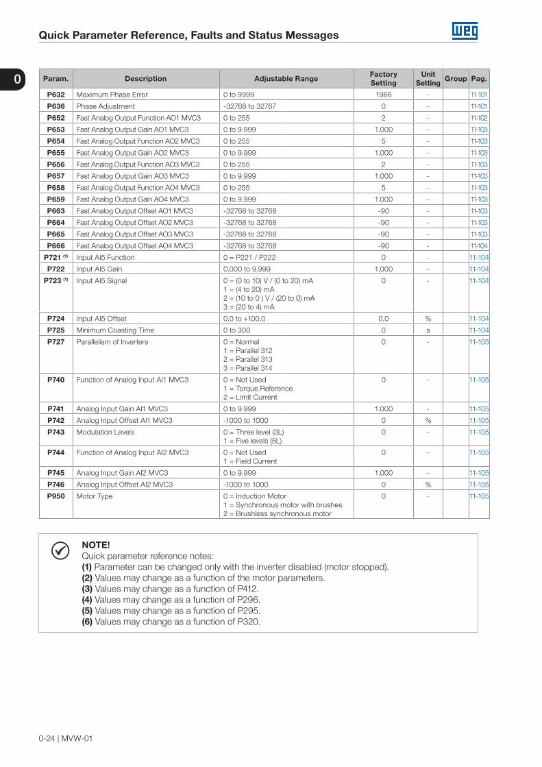
P632 Maximum Phase Error 0 to 9999 1966 - 11-101
P636 Phase Adjustment -32768 to 32767 0 - 11-101
P652 Fast Analog Output Function AO1 MVC3 0 to 255 2 - 11-102
P653 Fast Analog Output Gain AO1 MVC3 0 to 9.999 1.000 - 11-103
P654 Fast Analog Output Function AO2 MVC3 0 to 255 5 - 11-103
P655 Fast Analog Output Gain AO2 MVC3 0 to 9.999 1.000 - 11-103
P656 Fast Analog Output Function AO3 MVC3 0 to 255 2 - 11-103
P657 Fast Analog Output Gain AO3 MVC3 0 to 9.999 1.000 - 11-103
P658 Fast Analog Output Function AO4 MVC3 0 to 255 5 - 11-103
P659 Fast Analog Output Gain AO4 MVC3 0 to 9.999 1.000 - 11-103
P663 Fast Analog Output Offset AO1 MVC3 -32768 to 32768 -90 - 11-103
P664 Fast Analog Output Offset AO2 MVC3 -32768 to 32768 -90 - 11-103
P665 Fast Analog Output Offset AO3 MVC3 -32768 to 32768 -90 - 11-103
P666 Fast Analog Output Offset AO4 MVC3 -32768 to 32768 -90 - 11-104
P721 (1) Input AI5 Function 0 = P221 / P222 0 - 11-104
P722 Input AI5 Gain 0.000 to 9.999 1.000 - 11-104
P723 (1) Input AI5 Signal 0 = (0 to 10) V / (0 to 20) mA1 = (4 to 20) mA2 = (10 to 0 ) V / (20 to 0) mA3 = (20 to 4) mA
0 - 11-104
P724 Input AI5 Offset 0.0 to +100.0 0.0 % 11-104
P725 Minimum Coasting Time 0 to 300 0 s 11-104
P727 Parallelism of Inverters 0 = Normal1 = Parallel 3122 = Parallel 3133 = Parallel 314
0 - 11-105
P740 Function of Analog Input AI1 MVC3 0 = Not Used1 = Torque Reference2 = Limit Current
0 - 11-105
P741 Analog Input Gain AI1 MVC3 0 to 9.999 1.000 - 11-105
P742 Analog Input Offset AI1 MVC3 -1000 to 1000 0 % 11-105
P743 Modulation Levels 0 = Three level (3L)1 = Five levels (5L)
0 - 11-105
P744 Function of Analog Input AI2 MVC3 0 = Not Used1 = Field Current
0 - 11-105
P745 Analog Input Gain AI2 MVC3 0 to 9.999 1.000 - 11-105
P746 Analog Input Offset AI2 MVC3 -1000 to 1000 0 % 11-105
P950 Motor Type 0 = Induction Motor1 = Synchronous motor with brushes2 = Brushless synchronous motor
0 - 11-105
NOTE!Quick parameter reference notes:(1) Parameter can be changed only with the inverter disabled (motor stopped).(2) Values may change as a function of the motor parameters.(3) Values may change as a function of P412.(4) Values may change as a function of P296.(5) Values may change as a function of P295.(6) Values may change as a function of P320.

Quick Parameter Reference, Faults and Status Messages
MVW-01 | 0-25
0II. Messages of Alarms and Faults
The faults of the MVW-01 can be subdivided in Alarms (Axxx) and Faults (Fxxx). In general, the alarms serve to indicate a situation that, if it is not corrected, it can carry the inverter to stop by fault. A signalized fault indicates a situation that carried the inverter to be disabled (main breaker opening can or not ocurr, depending of the type of fault).
Table 1: Alarm and fault messages
Indication(A = Alarm / F = Fault) Meaning Page
A001 Mains low voltage 14-1A002 Mains high voltage 14-1F003 Mains undervoltage 14-1F004 Mains overvoltage 14-1F006 Mains unbalance / loss of phase 14-1F007 Mains voltage feedback fault 14-1A008 Line synchronism time-out 14-1A010 Rectifier high temperature 14-2F011 Rectifier overtemperature 14-2F012 Rectifier feedback temperature fault 14-2F013 Feedback missing on sinusoidal filter 14-2F014 Input circuit breaker closing failure 14-2F015 Input circuit breaker opening failure 14-2F016 External trip by input circuit breaker protection 14-2F017 Input circuit breaker not ready 14-2A018 Input transformer alarm 14-2F019 Input transformer fault 14-2F020 Pre-charge Fault 14-2F021 DC link undervoltage 14-2F022 DC link overvoltage 14-3F023 DC link imbalance 14-3F024 Link DC voltage feedback fault 14-3F025 Door closing fault 14-3F026 CB not ready 14-3F030 U 1 IGBT fault 14-3F031 U 2 IGBT fault 14-3F032 U 3 IGBT fault 14-3F033 U 4 IGBT fault 14-3F034 V 1 IGBT fault 14-3F035 V 2 IGBT fault 14-3F036 V 3 IGBT fault 14-3F037 V 4 IGBT fault 14-3F038 W 1 IGBT fault 14-3F039 W 2 IGBT fault 14-3F040 W 3 IGBT fault 14-3F041 W 4 IGBT fault 14-3F042 Braking IGBT 1 fault 14-3F043 Braking IGBT 2 fault 14-3F044 Arc detection 14-3F045 PS1/PS1S power supply fault 14-3A046 Alarm I x t 14-3F047 IGBT overload fault 14-3
F048 (5) Forced ventilation fault 14-3A050 U phase heatsink high temperature 14-3F051 U phase heatsink overtemperature 14-3F052 U phase heatsink temperature feedback fault 14-4A053 V phase heatsink high temperature 14-4F054 V phase heatsink overtemperature 14-4F055 V phase heatsink temperature feedback fault 14-4A056 W phase heatsink high temperature 14-4F057 W phase heatsink overtemperature 14-4F058 W phase heatsink temperature feedback fault 14-4

Quick Parameter Reference, Faults and Status Messages
0-26 | MVW-01
0 Indication(A = Alarm / F = Fault) Meaning Page
A059 BR phase heatsink high temperature 14-4F060 BR phase heatsink overtemperature 14-4F061 BR phase heatsink temperature feedback fault 14-4F062 Thermal imbalance between phases U, V and W 14-4F063 U output voltage feedback fault 14-4F064 V output voltage feedback fault 14-4F065 W output voltage feedback fault 14-4F066 Null current 14-4F068 Failure when entering in test mode 14-4F069 Calibration fault 14-4F070 Overcurrent / short circuit 14-5F071 Overcurrent at output 14-5
F072 (5) Overload I x t 14-5A073 Fault to ground alarm 14-5F074 Ground fault 14-5F075 Failure feedback of voltage between the Medium Point (MP) DC Link and ground 14-5F076 Motor connection open / Motor unbalanced current 14-5F077 Braking resistor overload 14-5
F078 (5) Motor overtemperature 14-5F079 (5) Encoder fault 14-5F080 CPU (watchdog) fault 14-6F081 Program memory fault 14-6
F082 (5) Copy function fault 14-6F083 (5) Programming fault 14-6F084 Auto-Diagnosis fault 14-6F085 Electronic power supply fault 14-6F087 Control boards communication fault 14-6
F090 (5) External defect (MVC4) fault 14-6F092 Pre-charge supply fault 14-6A093 Rectifier redundant ventilation failure alarm - set A 14-6A094 Inverter redundant ventilation failure alarm - set A 14-6F095 PS1 supply fault 14-6A096 Alarm 4 to 20 mA (current <3 mA) 14-6
F097 (5) Fault 4 to 20 mA 14-6A098 Not recorded help/Incompatible graphic HMI version 14-6F099 Invalid current offset 14-6F100 MVC3 fatal fault 14-6
F101 (5) Incompatible software version between boards 14-6F102 Unknown failure in EPLD of MVC3 14-6F103 MVC3 RAM fault 14-6F104 MVC3 A/D failure 14-6F105 EEPROM of MVC3 fault 14-6F106 MVC4 fatal fault 14-6A107 Alarm for WEG use 14-6A108 Not initialized inverter alarm 14-6F109 MVC3 external general disable fault 14-7A110 Motor overtemperature alarm 14-7A111 External defect alarm 14-7F112 Motor overspeed fault 14-7A113 Rectifier redundant ventilation failure alarm - set B 14-7A114 Inverter redundant ventilation failure alarm - set B 14-7F115 Communication fault between master rack and slave rack 14-7F116 Slave under fault condition 14-7F117 Current unbalance between slave drives 14-7A123 Programming Alarm 14-7A124 Parameter alteration with enabled inverter 14-7A125 Reading / writing in inexistent parameter 14-7A126 Value out of range 14-7A127 Function not configureted for Fieldbus 14-7A129 Inactive Fieldbus connection 14-7A130 Inactive Fieldbus board 14-7

Quick Parameter Reference, Faults and Status Messages
MVW-01 | 0-27
0Indication(A = Alarm / F = Fault) Meaning Page
A131 (1) Rectifier 1p high temperature 14-7F132 (1) Rectifier 1p overtemperature 14-7F133 (1) Rectifier 1p temperature feedback fault 14-7F134 (1) UAp 1 IGBT fault 14-8F135 (1) UAp 2 IGBT fault 14-8F136 (1) UAp 3 IGBT fault 14-8F137 (1) UAp 4 IGBT fault 14-8F138 (1) VAp 1 IGBT fault 14-8F139 (1) VAp 2 IGBT fault 14-8F140 (1) VAp 3 IGBT fault 14-8F141 (1) VAp 4 IGBT fault 14-8F142 (1) WAp 1 IGBT fault 14-8F143 (1) WAp 2 IGBT fault 14-8F144 (1) WAp 3 IGBT fault 14-8F145 (1) WAp 4 IGBT fault 14-8
F148 (1) (4) PS1 2 power supply fault 14-8A149 (1) UAp phase heatsink high temperature 14-8F150 (1) UAp phase heatsink overtemperature 14-8F151 (1) UAp phase heatsink temperature feedback fault 14-8A152 (1) VAp phase heatsink high temperature 14-8F153 (1) VAp phase heatsink overtemperature 14-8F154 (1) VAp phase heatsink temperature feedback fault 14-8A155 (1) WAp phase heatsink high temperature 14-8F156 (1) WAp phase heatsink overtemperature 14-8F157 (1) WAp phase heatsink temperature feedback fault 14-8A158 (1) BR B heatsink high temperature 14-9F159 (1) BR B heatsink overtemperature 14-9F160 (1) BR B heatsink temperature feedback fault 14-9F161 (1) Thermal imbalance between UAp, VAp and WAp phases 14-9F162 (1) UAp output voltage feedback fault 14-9F163 (1) VAp output voltage feedback fault 14-9F164 (1) WAp output voltage feedback fault 14-9A165 Safety Stop Active 14-9
F166 (2) Thermal imbalance among the UB, VB and WB phase heatsinks 14-9F167 (3) Thermal imbalance among the UBp, VBp and WBp phase heatsinks 14-9F168 Rectifier 123 thermal imbalance 14-9F169 Rectifier 123p thermal imbalance 14-9A170 Rectifier 2 high temperature 14-9
F171 (4) Rectifier 2 overtemperature 14-9F172 Rectifier 2 temperature feedback fault 14-9
A173 (4) Rectifier 3 high temperature 14-10F174 (4) Rectifier 3 overtemperature 14-10F175 (4) Rectifier 3 temperature feedback fault 14-10F176 (2) IGBT UB 1 fault 14-10F177 (2) IGBT UB 2 fault 14-10F178 (2) IGBT UB 3 fault 14-10F179 (2) IGBT UB 4 fault 14-10F180 (2) IGBT VB 1 fault 14-10F181 (2) IGBT VB 2 fault 14-10F182 (2) IGBT VB 3 fault 14-10F183 (2) IGBT VB 4 fault 14-10F184 (2) IGBT WB 1 fault 14-10F185 (2) IGBT WB 2 fault 14-10F186 (2) IGBT WB 3 fault 14-10F187 (2) IGBT WB 4 fault 14-10F188 (4) PS1 3 power supply fault 14-10A189 (2) UB phase heatsink high temperature 14-10F190 (2) UB phase heatsink overtemperature 14-10F191 (2) UB phase heatsink temperature feedback fault 14-10A192 (2) VB phase heatsink high temperature 14-10
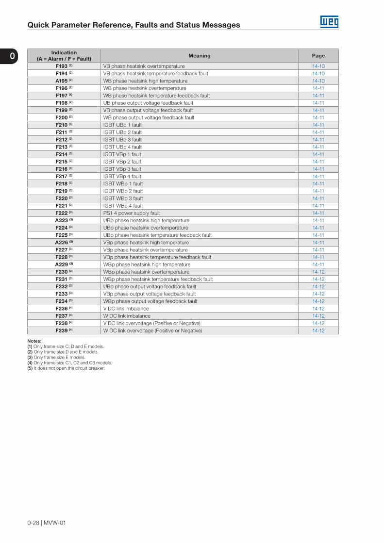
Quick Parameter Reference, Faults and Status Messages
0-28 | MVW-01
0 Indication(A = Alarm / F = Fault) Meaning Page
F193 (2) VB phase heatsink overtemperature 14-10F194 (2) VB phase heatsink temperature feedback fault 14-10A195 (2) WB phase heatsink high temperature 14-10F196 (2) WB phase heatsink overtemperature 14-11F197 (1) WB phase heatsink temperature feedback fault 14-11F198 (2) UB phase output voltage feedback fault 14-11F199 (2) VB phase output voltage feedback fault 14-11F200 (2) WB phase output voltage feedback fault 14-11F210 (3) IGBT UBp 1 fault 14-11F211 (3) IGBT UBp 2 fault 14-11F212 (3) IGBT UBp 3 fault 14-11F213 (3) IGBT UBp 4 fault 14-11F214 (3) IGBT VBp 1 fault 14-11F215 (3) IGBT VBp 2 fault 14-11F216 (3) IGBT VBp 3 fault 14-11F217 (3) IGBT VBp 4 fault 14-11F218 (3) IGBT WBp 1 fault 14-11F219 (3) IGBT WBp 2 fault 14-11F220 (3) IGBT WBp 3 fault 14-11F221 (3) IGBT WBp 4 fault 14-11F222 (3) PS1 4 power supply fault 14-11A223 (3) UBp phase heatsink high temperature 14-11F224 (3) UBp phase heatsink overtemperature 14-11F225 (3) UBp phase heatsink temperature feedback fault 14-11A226 (3) VBp phase heatsink high temperature 14-11F227 (3) VBp phase heatsink overtemperature 14-11F228 (3) VBp phase heatsink temperature feedback fault 14-11A229 (3) WBp phase heatsink high temperature 14-11F230 (3) WBp phase heatsink overtemperature 14-12F231 (3) WBp phase heatsink temperature feedback fault 14-12F232 (3) UBp phase output voltage feedback fault 14-12F233 (3) VBp phase output voltage feedback fault 14-12F234 (3) WBp phase output voltage feedback fault 14-12F236 (4) V DC link imbalance 14-12F237 (4) W DC link imbalance 14-12F238 (4) V DC link overvoltage (Positive or Negative) 14-12F239 (4) W DC link overvoltage (Positive or Negative) 14-12
Notes:(1) Only frame size C, D and E models.(2) Only frame size D and E models.(3) Only frame size E models.(4) Only frame size C1, C2 and C3 models.(5) It does not open the circuit breaker.
Safety Notices
MVW-01 | 1-1
1
1 SAFETY NOTICES
This manual contains the necessary information for the correct use of the MVW-01 Frequency Inverter.
It has been written for qualified personnel with suitable training or technical qualifications to operate this type ofequipment.
This manual presents all the functions and parameters of the MVW-01, but does not aim to present all the possible MVW-01 applications. WEG is not liable for applications not described in this manual.
This product is not intended for applications whose function is to ensure the physical integrity and/or the life of people, or any other application where failure of the MVW-01 can create a risk to the physical integrity and/or life of people. The designer who applies the MVW-01 must provide ways to ensure the safety of the installation even in the event of a drive failure.
1.1 SAFETY NOTICES IN THE MANUAL
Throughout this manual the following safety notes are used:
DANGER!The procedures recommended in this warning have the purpose of protecting the user against dead,serious injuries and considerable material damage.
DANGER!Les procédures concernées par cet avertissement sont destinées à protéger l'utilisateur contre des dangers mortels, des blessures et des détériorations matérielles importantes.
ATTENTION!The procedures recommended in this warning have the purpose of avoiding material damage.
NOTE!The text intents to supply important information for the correct understanding and good operationof the product.
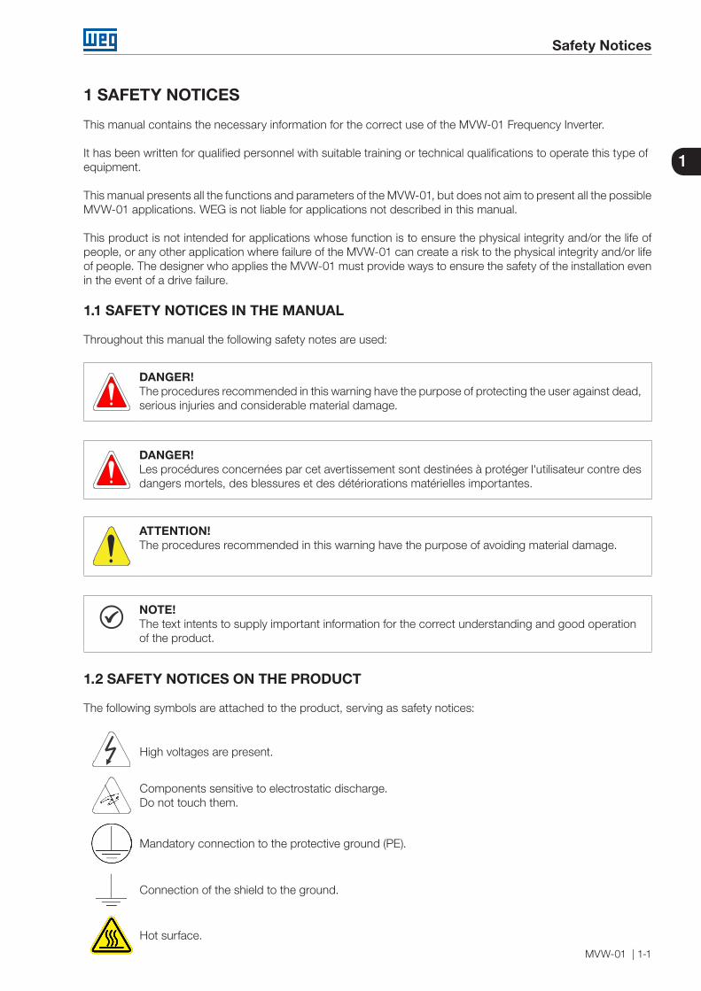
1.2 SAFETY NOTICES ON THE PRODUCT
The following symbols are attached to the product, serving as safety notices:
High voltages are present.
Components sensitive to electrostatic discharge.Do not touch them.
Mandatory connection to the protective ground (PE).
Connection of the shield to the ground.
Hot surface.
Safety Notices
1-2 | MVW-01
1
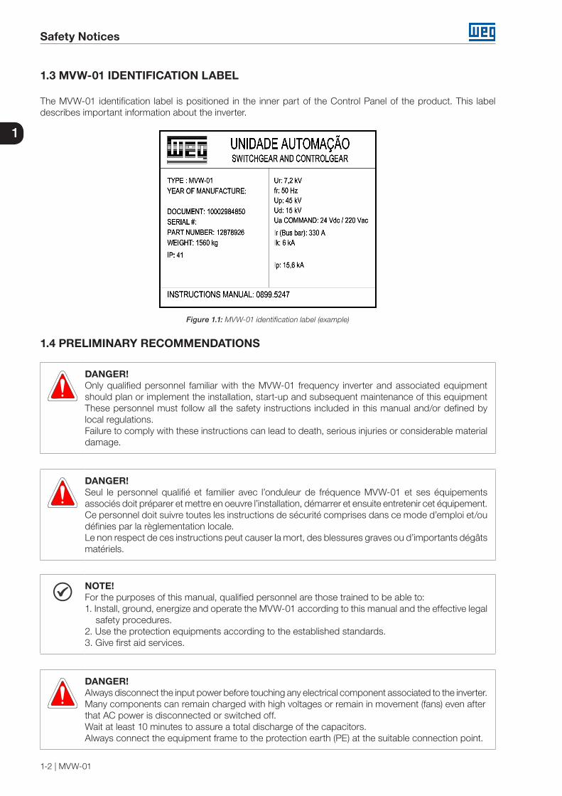
1.3 MVW-01 IDENTIFICATION LABEL
The MVW-01 identification label is positioned in the inner part of the Control Panel of the product. This label describes important information about the inverter.
Figure 1.1: MVW-01 identification label (example)
1.4 PRELIMINARY RECOMMENDATIONS
DANGER!Only qualified personnel familiar with the MVW-01 frequency inverter and associated equipment should plan or implement the installation, start-up and subsequent maintenance of this equipment These personnel must follow all the safety instructions included in this manual and/or defined by local regulations.Failure to comply with these instructions can lead to death, serious injuries or considerable material damage.
DANGER!Seul le personnel qualifié et familier avec l’onduleur de fréquence MVW-01 et ses équipements associés doit préparer et mettre en oeuvre l’installation, démarrer et ensuite entretenir cet équipement.Ce personnel doit suivre toutes les instructions de sécurité comprises dans ce mode d’emploi et/ou définies par la règlementation locale.Le non respect de ces instructions peut causer la mort, des blessures graves ou d’importants dégâts matériels.
NOTE!For the purposes of this manual, qualified personnel are those trained to be able to:1. Install, ground, energize and operate the MVW-01 according to this manual and the effective legal
safety procedures.2. Use the protection equipments according to the established standards.3. Give first aid services.
DANGER!Always disconnect the input power before touching any electrical component associated to the inverter.Many components can remain charged with high voltages or remain in movement (fans) even afterthat AC power is disconnected or switched off.Wait at least 10 minutes to assure a total discharge of the capacitors.Always connect the equipment frame to the protection earth (PE) at the suitable connection point.

Safety Notices
MVW-01 | 1-3
1
DANGER!Débranchez toujours l'alimentation générale avant de toucher un composant électrique associé au convertisseur. Nombreux composants peuvent rester chargés avec haute tension et/ou en mouvement (ventilateurs), même après que l'entrée d'alimentation CA a été débranchée ou coupée. Attendez au moins 10 minutes pour s'assurer de la décharge totale des condensateurs. Connectez toujours le boîtier de l'équipement à terre de protection (PE) au point adéquat pour ça.
ATTENTION!Electronic boards have components sensitive to electrostatic discharges. Do not touch directly on components or connectors. If necessary, touch the grounded metallic frame before or use an adequate grounded wrist strap.
Do not perform any high pot tests with the inverter!If it is necessary consult WEG.
NOTE!Frequency inverter may interfere with other electronic equipment. In order to reduce these effects, takethe precautions recommended.
NOTE!Read the user's manual completely before installing or operating the inverter.

Safety Notices
1-4 | MVW-01
1
General Information
MVW-01 | 2-1
2
2 GENERAL INFORMATION
This chapter defines the contents and the purpose of this manual and describes the main characteristics of the MVW-01 frequency inverter and how to identify its components. It provides also additional information on the receiving and storage of the product.
2.1 ABOUT THIS MANUAL
This manual presents 14 chapters, which have a logical sequence so that the user receives, installs, programs and operates the MVW01:Chapter 1 SAFETY NOTICES on page 1-1.Chapter 2 GENERAL INFORMATION on page 2-1.Chapter 3 MVW-01 WITH 3 LEVELS (3L) on page 3-1.Chapter 4 MVW-01 WITH 5 LEVELS (5L) on page 4-1.Chapter 5 MVW-01C (COMPACT) on page 5-1.Chapter 6 INVERTER PARALLELISM on page 6-1.Chapter 7 SYNCHRONOUS MOTOR LINE on page 7-1.Chapter 8 INSTALLATION, CONNECTION AND ENERGIZATION on page 8-1.Chapter 9 KEYPAD (HMI) OPERATION on page 9-1.Chapter 10 OPTIONAL ACCESSORIES AND BOARDS on page 10-1.Chapter 11 DETAILED PARAMETER DESCRIPTION on page 11-1.Chapter 12 SPECIAL FUNCTIONS on page 12-1.Chapter 13 COMMUNICATION NETWORKS on page 13-1.Chapter 14 DIAGNOSTICS AND TROUBLESHOOTING on page 14-1.
This user's manual contains information about WEG MVW-01 Medium Voltage Inverter. This document is arranged in dedicated and specific chapters to explain the proper handling, installation, parameterization, care, troubleshooting, adaption to applications and functionalities of the equipment.
The characteristics and recommendations contained in this manual were based on models of the standard MVW-01. It is worth of notice that, in addition to supplying standard products, WEG technical team composed of distinct departments (Technical Sales, Contract Management, Engineering, Technical Assistance, among others) is qualified to develop and provide customized solutions according to the needs of its customers and specific applications.
The MVW-01 product can be customized (engineered) to meet the needs and technical specifications of our customers. Variations is sizes, technical recommendations, performance data and necessity to add optional items are possible in relation to the information contained in this document.
Besides the user's manual, the Supply Project is part of the documentation delivered to the customer. This project contains all the electrical, mechanical and parameterization information, as well as instructions for the interface/installation with other equipment regarding the MVW-01 supplied.
The MVW-01, as well as other WEG products, is in constant evolution in relation to both its internal parts (hardware) and its programming (software/firmware). Any question about the equipment and its documentation can be answered by means of WEG communication channels.
WEG is not liable for the improper use of the information contained in this manual.
2.2 SOFTWARE VERSION
It is important to note the software version installed in the MVW-01, since it defines the functions and the programming parameters of the inverter. This manual refers to the firmware version as stated in the inside cover. For instance, the version 3.2X means from 3.20 to 3.29, where “X” are evolutions in the firmware that do not affect the contents of this manual.
In the version 3.2X, the new control boards MVC4 and Graphic HMI 2 (HMIG2) have exactly the same functions of the MVC2 boards and conventional Graphic HMI in the 1.9X version; therefore, there are no additional remarks about these boards.

General Information
2-2 | MVW-01
2
2.3 HOW TO SPECIFY THE MVW-01 MODEL
POWER SUPPLY
Voltage 2300, 3300, 4160 V, 4600 or 6900 V (± 10 %, -20 % with output power reduction).Frequency 50 or 60 Hz (specify) ±3 %.Voltage imbalancebetween phases
<3 %.
Cos j >0.97.Overvoltage category Category III.
AUXILIARY SUPPLY
Voltage 220, 380, 400, 415, 440, 460 or 480 V.Frequency 50 or 60 Hz (±3 %).Voltage imbalancebetween phase
<3 %.
PROTECTIONDEGREE
Standard IP41.
DIMENSIONWidth / Height / Depth (mm)
8 distinct frame sizes.
ENVIRONMENTALCONDITIONS
Temperature 0 to 40 °C (up to 50 °C with 2.5 % reduction in the output current/ °C).Humidity 5 to 90 % without condensation.Altitude 0 to 1000 m (up to 4000 m with 10 % reduction in the output current / 1000 m).Pollution degree 2.
FINISHING Color Gray ultra dull (Doors). Blue ultra dull (Base, Roof, Shutters).
CONTROL
Microprocessor 32 bits.
Control method Sinusoidal PWM with Space Vector Modulation (SVM) and Optimized Pulse Patterns
(OPP) Digital.Control types Scalar (Imposed Voltage - V/F), Vector (encoder and sensorless).
High voltage IGBT transistor IGBT (HV - IGBT).SwitchingFrequency range 0 to 120 Hz.
Allowed overload 150 % during 60 seconds, every 10 minutes (1.5 x Inom. - HD). 115 % during 60 seconds, every 10 minutes (1.15 x Inom. - ND).
Efficiency Higher 98.5 %.
PERFORMANCE Speed control
V/F Regulation 1 % of the nominal speed with slip compensation. Resolution: 1 rpm (keypad reference).
Sensorless Regulation: 0.5 % of the nominal speed. Speed variation range: 1:100.
With Encoder (using EBA or EBB board)
Regulation:±0.01 % of the nominal speed with a 14-bit analog input (EBA).±0.01 % of the nominal speed with digital reference (keypad, Serial, Fieldbus, Electronic Potentiometer, Multispeed).
±0.1 % of nominal speed with 10-bit analog input (CC9).
INPUTSOUTPUTS
Analogical
2 programmable differential inputs (10 bits): 0 to 10 V, 0 to 20 mA or 4 to 20 mA. 1 programmable bipolar input (14 bits): -10 to +10 V, 0 to 20 mA or 4 to 20 mA. 1 programmable isolated input (10 bits): 0 to 10 V, 0 to 20 mA or 4 to 20 mA. 1 programmable isolated input (10 bits): 0 to 10 V, 0 to 20 mA or 4 to 20 mA. 2 programmable outputs (11 bits): 0 to 10 V. 2 bipolar programmable outputs (14 bits): (-10 to +10) V. 2 programmable isolated outputs (11 bits): 0 to 20 mA or 4 to 20 mA. 2 programmable isolated outputs (11 bits): 0 to 20 mA or 4 to 20 mA.
Digital AnalogRelay Transistor
8 programmable isolated inputs: 24 Vdc. 1 programmable isolated input: 24 Vdc. 1 programmable isolated input: 24 Vdc (for motor PTC thermistor). 5 programmable outputs, contacts NO/NC: 240 Vac, 1 A. 2 programmable isolated open collector outputs: 24 Vdc, 50 mA.
COMMUNICATIONSerial InterfaceFieldbus Networks
RS-232 (point to point). RS-485, isolated, via EBA or EBB board (multipoint up to 30 inverters). Modbus RTU (incorporated software) via RS-485 serial interface. Profibus DP or DeviceNet via additional KFB kits. Ethernet.
General Information
MVW-01 | 2-3
2
SAFETY
Protections (memoryof the last 100 faults/alarms with date and time)
DC link overvoltage. Short-circuit at the output. DC link undervoltage. Phase-ground short-circuit at the output. Overtemperature at the inverter and at
the motor. External fault.
Overcurrent at the output. Auto-diagnosis fault and programming error.
Motor overload (I x t). Serial communication fault. Braking resistor overload. Phase loss at the input. CPU (watchdog)/EEPROM fault. HMI-MVW-01 interface connection fault. Incremental encoder fault.
APPLICABLESTANDARDS
Electromagneticcompatibility
EMC directive 89 / 336 / EEC – industrial environment. EN 61800-3 (EMC - Emission and Immunity) standard.
CEI - IEC 61800 Adjustable Speed Electrical Power Drive System. Part 4 - General Requirements. Part 5 - Safety Requirements.
HUMAN MACHINEINTERFACE(LCD DISPLAY)
Command Start/Stop, Parameterization (Programming of general functions). Increase/decrease the speed. JOG, Forward/Reverse selection, Local/Remote selection.
Supervision (Reading)
Speed reference (rpm). Motor speed (rpm). Value proportional to the speed (e.g.: m/min). Motor frequency (Hz). TDC link voltage (V). Motor torque %. Output power (kW). Energized time (h). Operation time (h). Motor current (A). Motor voltage (V). Inverter status. Digital input status. Digital output (transistor) status. Relay output status. Analog input values. 100 last erros in the memory with date and time. Fault/alarm messages.
AVAILABLERESOURCES/FUNCTIONS
Options
Blank cover for local HMI. Blank cover for remote HMI. Frame kit for remote interface. Frame kit for remote interface. Fieldbus network communication kits (internal
inverter installation). Profibus DP.
Fieldbus network communication kits (internal inverter installation).
DeviceNet.
SuperDrive kit with RS-232 serial communication interface (Inverter - PC). Ethernet kit. I/O expansion kit.
2.3.1 Available Models
Nowadays, the MVW-01 medium voltage inverter line can be divided in 2 distinct generations, G1 and G2. The second generation (G2) is based in the use of semiconductor devices with higher current capacity and efficiency, besides an improvement in the inverter cooling system. These combined features resulted in the increase of the power density of the inverters, now named MVW-01 G2.
The next tables present the available models for both generations, and in the same generation the models are subdivided by their topology of 3 levels (3L) or 5 levels (5L).
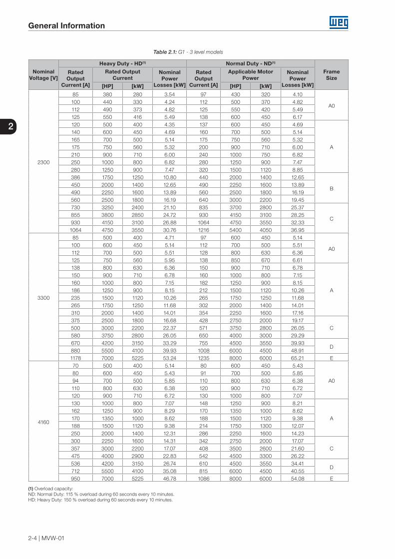
General Information
2-4 | MVW-01
2
Table 2.1: G1 - 3 level models
NominalVoltage [V]
Heavy Duty - HD(1) Normal Duty - ND(1)
FrameSize
RatedOutput
Current [A]
Rated OutputCurrent
NominalPower
Losses [kW]
RatedOutput
Current [A]
Applicable MotorPower
NominalPower
Losses [kW][HP] [kW] [HP] [kW]
2300
85 380 280 3.54 97 430 320 4.10
A0100 440 330 4.24 112 500 370 4.82112 490 373 4.82 125 550 420 5.49125 550 416 5.49 138 600 450 6.17120 500 400 4.35 137 600 450 4.69
A
140 600 450 4.69 160 700 500 5.14165 700 500 5.14 175 750 560 5.32175 750 560 5.32 200 900 710 6.00210 900 710 6.00 240 1000 750 6.82250 1000 800 6.82 280 1250 900 7.47280 1250 900 7.47 320 1500 1120 8.85386 1750 1250 10.80 440 2000 1400 12.65
B450 2000 1400 12.65 490 2250 1600 13.89490 2250 1600 13.89 560 2500 1800 16.19560 2500 1800 16.19 640 3000 2200 19.45730 3250 2400 21.10 835 3700 2800 25.37
C855 3800 2850 24.72 930 4150 3100 28.25930 4150 3100 26.88 1064 4750 3550 32.331064 4750 3550 30.76 1216 5400 4050 36.95
3300
85 500 400 4.71 97 600 450 5.14
A0100 600 450 5.14 112 700 500 5.51112 700 500 5.51 128 800 630 6.36125 750 560 5.95 138 850 670 6.61138 800 630 6.36 150 900 710 6.78
A
150 900 710 6.78 160 1000 800 7.15160 1000 800 7.15 182 1250 900 8.15186 1250 900 8.15 212 1500 1120 10.26235 1500 1120 10.26 265 1750 1250 11.68265 1750 1250 11.68 302 2000 1400 14.01310 2000 1400 14.01 354 2250 1600 17.16375 2500 1800 16.68 428 2750 2000 19.17
C500 3000 2200 22.37 571 3750 2800 26.05580 3750 2800 26.05 650 4000 3000 29.29670 4200 3150 33.29 755 4500 3550 39.93
D880 5500 4100 39.93 1008 6000 4500 48.911178 7000 5225 53.24 1235 8000 6000 65.21 E
4160
70 500 400 5.14 80 600 450 5.43
A080 600 450 5.43 91 700 500 5.8594 700 500 5.85 110 800 630 6.38110 800 630 6.38 120 900 710 6.72120 900 710 6.72 130 1000 800 7.07130 1000 800 7.07 148 1250 900 8.21
A162 1250 900 8.29 170 1350 1000 8.62170 1350 1000 8.62 188 1500 1120 9.38188 1500 1120 9.38 214 1750 1300 12.07250 2000 1400 12.31 286 2250 1600 14.23300 2250 1600 14.31 342 2750 2000 17.07
C357 3000 2200 17.07 408 3500 2600 21.60475 4000 2900 22.83 542 4500 3300 26.22536 4200 3150 26.74 610 4500 3550 34.41
D712 5500 4100 35.08 815 6000 4500 40.55950 7000 5225 46.78 1086 8000 6000 54.08 E
(1) Overload capacity:ND: Normal Duty: 115 % overload during 60 seconds every 10 minutes.HD: Heavy Duty: 150 % overload during 60 seconds every 10 minutes.

General Information
MVW-01 | 2-5
2
Table 2.2: G1 - 5 level models
NominalVoltage [V]
Heavy Duty - HD(1) Normal Duty - ND(1)
FrameSize
RatedOutput
Current [A]
Applicable MotorPower
NominalPower
Losses [kW]
RatedOutput
Current [A]
Applicable MotorPower
NominalPower
Losses [kW][HP] [kW] [HP] [kW]
6000~6300
44 420 320 8.12 58 500 373 9.44
C159 500 373 9.54 78 750 560 11.4479 750 560 11.55 104 1000 750 14.2395 900 680 13.24 124 1500 1120 16.52107 1000 750 14.57 140 1750 1300 18.45
6600~6900
40 420 320 8.11 53 500 373 9.36
C153 500 373 9.36 70 750 560 11.0872 750 560 11.29 94 1000 750 13.6785 900 680 12.68 112 1500 1120 15.7399 1000 750 14.23 130 1750 1300 17.89
(1) Overload capacity:ND: Normal Duty: 115 % overload during 60 seconds every 10 minutes.HD: Heavy Duty: 150 % overload during 60 seconds every 10 minutes.
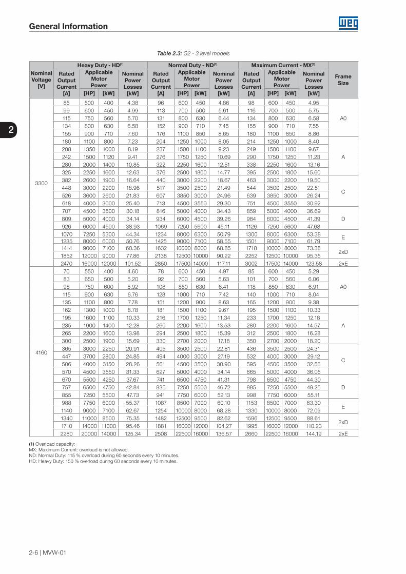
General Information
2-6 | MVW-01
2
Table 2.3: G2 - 3 level models
NominalVoltage
[V]
Heavy Duty - HD(1) Normal Duty - ND(1) Maximum Current - MX(1)
FrameSize
RatedOutputCurrent
[A]
ApplicableMotorPower
NominalPowerLosses
[kW]
RatedOutputCurrent
[A]
ApplicableMotorPower
NominalPowerLosses
[kW]
RatedOutputCurrent
[A]
ApplicableMotorPower
NominalPowerLosses
[kW][HP] [kW] [HP] [kW] [HP] [kW]
3300
85 500 400 4.38 96 600 450 4.86 98 600 450 4.95
A099 600 450 4.99 113 700 500 5.61 116 700 500 5.75115 750 560 5.70 131 800 630 6.44 134 800 630 6.58134 800 630 6.58 152 900 710 7.45 155 900 710 7.55155 900 710 7.60 176 1100 850 8.65 180 1100 850 8.86180 1100 800 7.23 204 1250 1000 8.05 214 1250 1000 8.40
A208 1350 1000 8.19 237 1500 1100 9.23 249 1500 1100 9.67242 1500 1120 9.41 276 1750 1250 10.69 290 1750 1250 11.23280 2000 1400 10.85 322 2250 1600 12.51 338 2250 1600 13.16325 2250 1600 12.63 376 2500 1800 14.77 395 2500 1800 15.60382 2600 1900 16.64 440 3000 2200 18.67 463 3000 2200 19.50
C448 3000 2200 18.96 517 3500 2500 21.49 544 3500 2500 22.51526 3600 2600 21.83 607 3850 3000 24.96 639 3850 3000 26.24618 4000 3000 25.40 713 4500 3550 29.30 751 4500 3550 30.92707 4500 3500 30.18 816 5000 4000 34.43 859 5000 4000 36.69
D809 5000 4000 34.14 934 6000 4500 39.26 984 6000 4500 41.39926 6000 4500 38.93 1069 7250 5600 45.11 1126 7250 5600 47.681070 7250 5300 44.34 1234 8000 6300 50.79 1300 8000 6300 53.38 E1235 8000 6000 50.76 1425 9000 7100 58.55 1501 9000 7100 61.791414 9000 7100 60.36 1632 10000 8000 68.85 1718 10000 8000 73.38
2xD1852 12000 9000 77.86 2138 12500 10000 90.22 2252 12500 10000 95.352470 16000 12000 101.52 2850 17500 14000 117.11 3002 17500 14000 123.58 2xE
4160
70 550 400 4.60 78 600 450 4.97 85 600 450 5.29
A083 650 500 5.20 92 700 560 5.63 101 700 560 6.0698 750 600 5.92 108 850 630 6.41 118 850 630 6.91115 900 630 6.76 128 1000 710 7.42 140 1000 710 8.04135 1100 800 7.78 151 1200 900 8.63 165 1200 900 9.38162 1300 1000 8.78 181 1500 1100 9.67 195 1500 1100 10.33
A195 1600 1100 10.33 216 1700 1250 11.34 233 1700 1250 12.18235 1900 1400 12.28 260 2200 1600 13.53 280 2200 1600 14.57265 2200 1600 13.98 294 2500 1800 15.39 312 2500 1800 16.28300 2500 1900 15.69 330 2700 2000 17.18 350 2700 2000 18.20365 3000 2250 20.91 405 3500 2500 22.81 436 3500 2500 24.31
C447 3700 2800 24.85 494 4000 3000 27.19 532 4000 3000 29.12506 4000 3150 28.26 561 4500 3500 30.90 595 4500 3500 32.56570 4500 3550 31.33 627 5000 4000 34.14 665 5000 4000 36.05670 5500 4250 37.67 741 6500 4750 41.31 798 6500 4750 44.30
D757 6500 4750 42.84 835 7250 5500 46.72 885 7250 5500 49.25855 7250 5500 47.73 941 7750 6000 52.13 998 7750 6000 55.11988 7750 6000 55.37 1087 8500 7000 60.10 1153 8500 7000 63.30
E1140 9000 7100 62.67 1254 10000 8000 68.28 1330 10000 8000 72.091340 11000 8500 75.35 1482 12500 9500 82.62 1596 12500 9500 88.61
2xD1710 14000 11000 95.46 1881 16000 12000 104.27 1995 16000 12000 110.232280 20000 14000 125.34 2508 22500 16000 136.57 2660 22500 16000 144.19 2xE
(1) Overload capacity:MX: Maximum Current: overload is not allowed.ND: Normal Duty: 115 % overload during 60 seconds every 10 minutes.HD: Heavy Duty: 150 % overload during 60 seconds every 10 minutes.
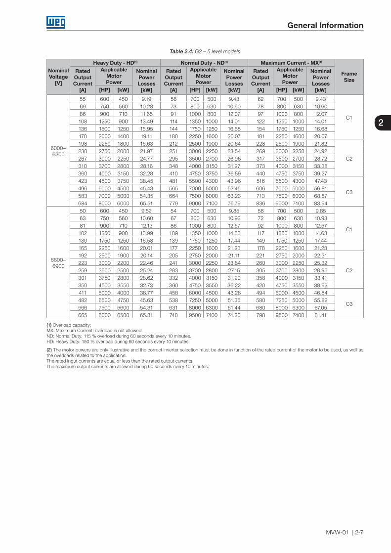
General Information
MVW-01 | 2-7
2
Table 2.4: G2 – 5 level models
NominalVoltage
[V]
Heavy Duty - HD(1) Normal Duty - ND(1) Maximum Current - MX(1)
FrameSize
RatedOutputCurrent
[A]
ApplicableMotorPower
NominalPowerLosses
[kW]
RatedOutputCurrent
[A]
ApplicableMotorPower
NominalPowerLosses
[kW]
RatedOutputCurrent
[A]
ApplicableMotorPower
NominalPowerLosses
[kW][HP] [kW] [HP] [kW] [HP] [kW]
6000~6300
55 600 450 9.19 58 700 500 9.43 62 700 500 9.43
C1
69 750 560 10.28 73 800 630 10.60 78 800 630 10.6086 900 710 11.65 91 1000 800 12.07 97 1000 800 12.07108 1250 900 13.49 114 1350 1000 14.01 122 1350 1000 14.01136 1500 1250 15.95 144 1750 1250 16.68 154 1750 1250 16.68170 2000 1400 19.11 180 2250 1600 20.07 181 2250 1600 20.07198 2250 1800 16.63 212 2500 1900 20.64 228 2500 1900 21.82
C2230 2750 2000 21.97 251 3000 2250 23.54 269 3000 2250 24.92267 3000 2250 24.77 295 3500 2700 26.96 317 3500 2700 28.72310 3700 2800 28.16 348 4000 3150 31.27 373 4000 3150 33.38360 4000 3150 32.28 410 4750 3750 36.59 440 4750 3750 39.27423 4500 3750 38.45 481 5500 4300 43.96 516 5500 4300 47.43
C3496 6000 4500 45.43 565 7000 5000 52.45 606 7000 5000 56.81583 7000 5000 54.35 664 7500 6000 63.23 713 7500 6000 68.87684 8000 6000 65.51 779 9000 7100 76.79 836 9000 7100 83.94
6600~6900
50 600 450 9.52 54 700 500 9.85 58 700 500 9.85
C1
63 750 560 10.60 67 800 630 10.93 72 800 630 10.9381 900 710 12.13 86 1000 800 12.57 92 1000 800 12.57102 1250 900 13.99 109 1350 1000 14.63 117 1350 1000 14.63130 1750 1250 16.58 139 1750 1250 17.44 149 1750 1250 17.44165 2250 1600 20.01 177 2250 1600 21.23 178 2250 1600 21.23192 2500 1900 20.14 205 2750 2000 21.11 221 2750 2000 22.31
C2223 3000 2200 22.46 241 3000 2250 23.84 260 3000 2250 25.32259 3500 2500 25.24 283 3700 2800 27.15 305 3700 2800 28.95301 3750 2800 28.62 332 4000 3150 31.20 358 4000 3150 33.41350 4500 3550 32.73 390 4750 3550 36.22 420 4750 3550 38.92411 5000 4000 38.77 458 6000 4500 43.26 494 6000 4500 46.84
C3482 6500 4750 45.63 538 7250 5000 51.35 580 7250 5000 55.82566 7500 5600 54.31 631 8000 6300 61.44 680 8000 6300 67.05665 8000 6500 65.31 740 9500 7400 74.20 798 9500 7400 81.41
(1) Overload capacity:MX: Maximum Current: overload is not allowed.ND: Normal Duty: 115 % overload during 60 seconds every 10 minutes.HD: Heavy Duty: 150 % overload during 60 seconds every 10 minutes.
(2) The motor powers are only illustrative and the correct inverter selection must be done in function of the rated current of the motor to be used, as well as the overloads related to the application.The rated input currents are equal or less than the rated output currents.The maximum output currents are allowed during 60 seconds every 10 minutes.
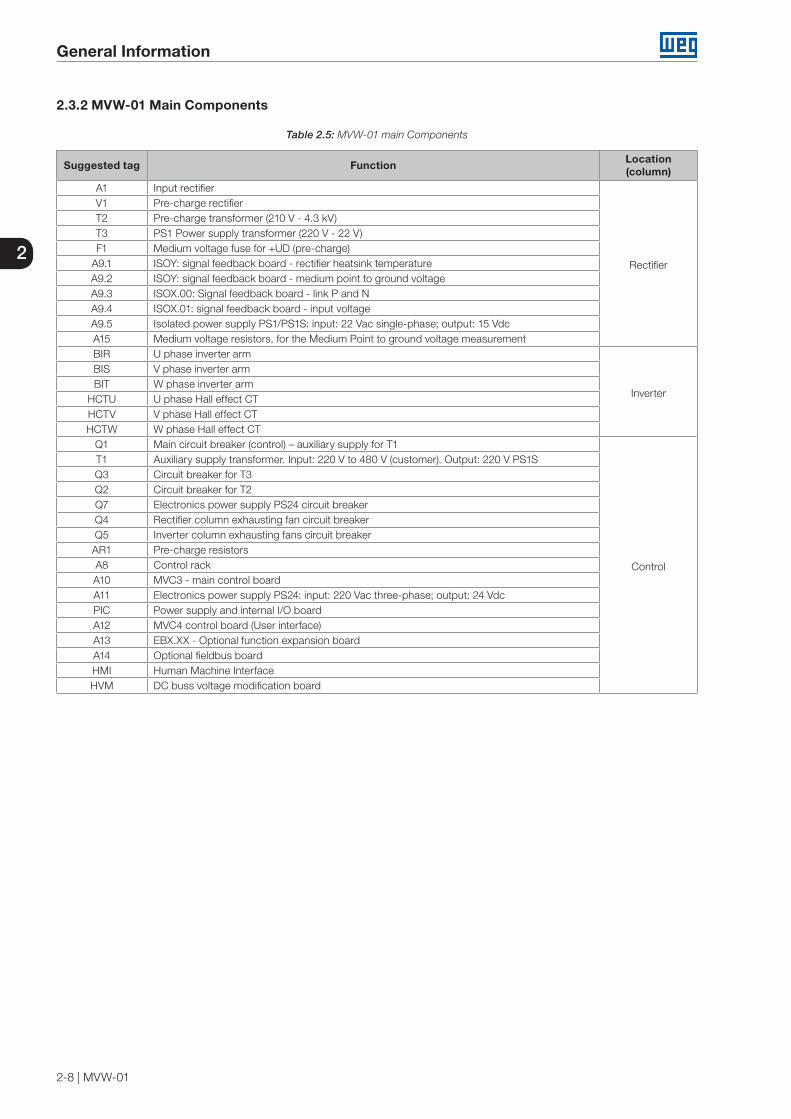
General Information
2-8 | MVW-01
2
2.3.2 MVW-01 Main Components
Table 2.5: MVW-01 main Components
Suggested tag Function Location(column)
A1 Input rectifier
Rectifier
V1 Pre-charge rectifierT2 Pre-charge transformer (210 V - 4.3 kV)T3 PS1 Power supply transformer (220 V - 22 V)F1 Medium voltage fuse for +UD (pre-charge)
A9.1 ISOY: signal feedback board - rectifier heatsink temperatureA9.2 ISOY: signal feedback board - medium point to ground voltageA9.3 ISOX.00: Signal feedback board - link P and NA9.4 ISOX.01: signal feedback board - input voltageA9.5 Isolated power supply PS1/PS1S: input: 22 Vac single-phase; output: 15 VdcA15 Medium voltage resistors, for the Medium Point to ground voltage measurementBIR U phase inverter arm
Inverter
BIS V phase inverter armBIT W phase inverter arm
HCTU U phase Hall effect CTHCTV V phase Hall effect CTHCTW W phase Hall effect CT
Q1 Main circuit breaker (control) – auxiliary supply for T1
Control
T1 Auxiliary supply transformer. Input: 220 V to 480 V (customer). Output: 220 V PS1SQ3 Circuit breaker for T3Q2 Circuit breaker for T2Q7 Electronics power supply PS24 circuit breakerQ4 Rectifier column exhausting fan circuit breakerQ5 Inverter column exhausting fans circuit breakerAR1 Pre-charge resistorsA8 Control rackA10 MVC3 - main control boardA11 Electronics power supply PS24: input: 220 Vac three-phase; output: 24 VdcPIC Power supply and internal I/O boardA12 MVC4 control board (User interface)A13 EBX.XX - Optional function expansion boardA14 Optional fieldbus boardHMI Human Machine InterfaceHVM DC buss voltage modification board
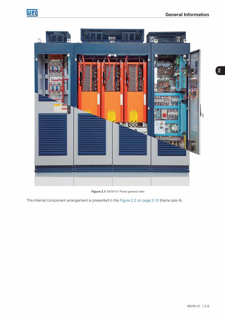
General Information
MVW-01 | 2-9
2
Figure 2.1: MVW-01 Panel general view
The internal component arrangement is presented in the Figure 2.2 on page 2-10 (frame size A).
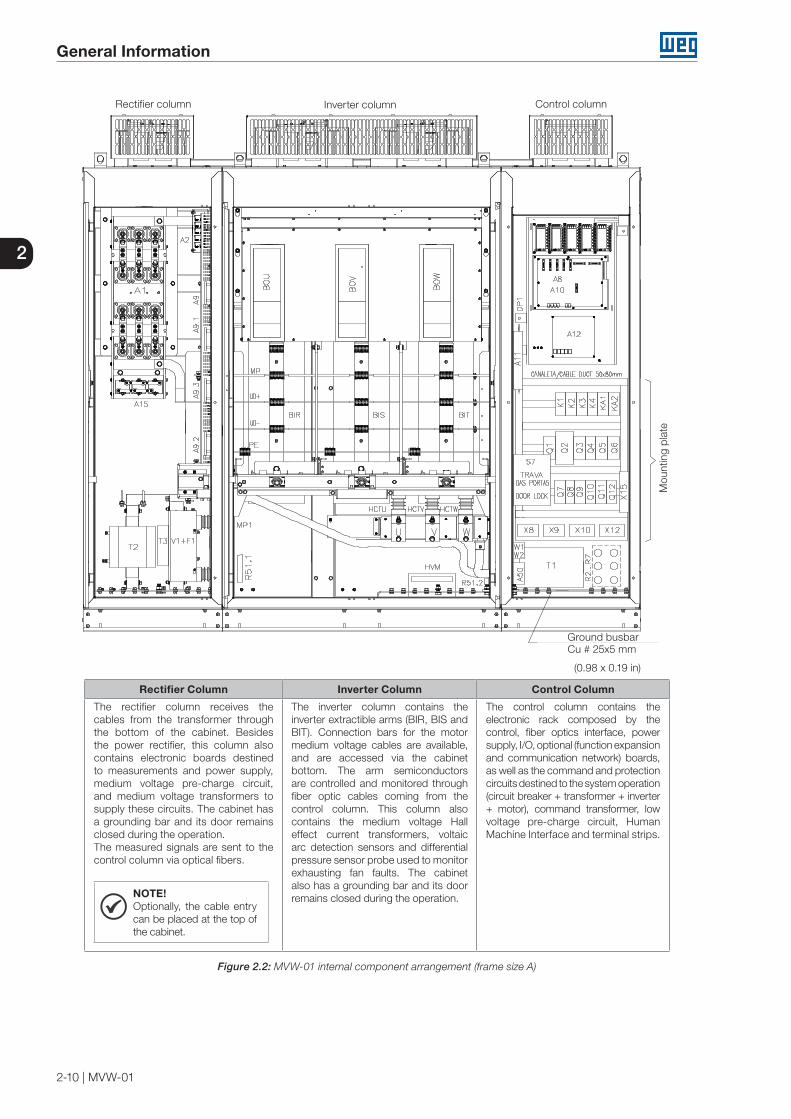
General Information
2-10 | MVW-01
2
Rectifier column
Mou
ntin
g pl
ate
Inverter column Control column
Ground busbarCu # 25x5 mm
(0.98 x 0.19 in)
Rectifier Column Inverter Column Control Column
The rectifier column receives the cables from the transformer through the bottom of the cabinet. Besides the power rectifier, this column also contains electronic boards destined to measurements and power supply, medium voltage pre-charge circuit, and medium voltage transformers to supply these circuits. The cabinet has a grounding bar and its door remains closed during the operation.The measured signals are sent to the control column via optical fibers.
NOTE!Optionally, the cable entry can be placed at the top of the cabinet.
The inverter column contains the inverter extractible arms (BIR, BIS and BIT). Connection bars for the motor medium voltage cables are available, and are accessed via the cabinet bottom. The arm semiconductors are controlled and monitored through fiber optic cables coming from the control column. This column also contains the medium voltage Hall effect current transformers, voltaic arc detection sensors and differential pressure sensor probe used to monitor exhausting fan faults. The cabinet also has a grounding bar and its door remains closed during the operation.
The control column contains the electronic rack composed by the control, fiber optics interface, power supply, I/O, optional (function expansion and communication network) boards, as well as the command and protection circuits destined to the system operation (circuit breaker + transformer + inverter + motor), command transformer, low voltage pre-charge circuit, Human Machine Interface and terminal strips.
Figure 2.2: MVW-01 internal component arrangement (frame size A)

General Information
MVW-01 | 2-11
2
2.3.3 MVW-01 Electronic boards
Table 2.6: MVW-01 electronic boards
Name Function Panel / Module1 MVC3 Main control
Control / A8 Rack
2 MVC4 User interface control3 FOI 3, 4 It converts electrical signals into optical signals and vice versa4 PIC2 Power supplies for the electronics, internal use digital inputs and output relays5 EBA, EBB, EBC Optional function expansion boards6 Fieldbus Optional network communication boards
7 ISOY/ISOZ Signal feedback boards, they measure medium voltages or temperatures and sendthe information via optical signals (1 channel)
Rectifier / A9
8 ISOX Signal feedback boards, they measure medium voltages or temperatures and sendthe information via optical signals (2 channels)
Rectifier / A9
9 PS24Electronics power supply:- input: 220 Vac 3 ~ or 220 Vac 1~- output: 24 Vdc
Control / A11
10 PS1/PS1SIsolated power supply:- input: 22 Vac 1 ~ (PST) 220 Vac 1~ (PSTS) output: 15 Vdc
Rectifier / A9.5
11 HVM It indicates that the DC link is energized(Neon lamps)
Inverter(visible in the control)
121SD210F21SP0335
Gate drivers Inverter / BIR, BIS,BIT
13 PLC2 PLC expansion board - optional Control / A8 Rack14 RSSI Absolute encoder interface - optional Control15 HMI Cables
2.3.4 PLC2 Expansion Board
The PLC2 board presents the following hardware features:
Table 2.7: PLC2
COMMUNICATION Serial Interface CANopen Master/Slave and DeviceNet Slave networks. Optional for Profibus DP Slave network. Optional for DeviceNet Slave network.
INPUT
Analog 1 differential analog input (-10 to +10) Vdc or (-20 to +20) mA, 14 bits.Incremental Encoder 2 isolated encoder inputs, with external supply of 5 Vdc or (8 to 24) Vdc.
Digital 9 isolated digital inputs, bidirectional, 24 Vdc. 1 motor PTC input.
OUTPUT
Analog 2 analog outputs (-10 to +10) Vdc or (0 to 20) mA, 12 bits.Serial Interface 1 serial communication interface - RS-232C (Standard protocol: MODBUS-RTU).
Digital 3 relay outputs: 250 V x 3 A. 3 optocoupled digital outputs, bidirectional, 24 Vdc x 500 mA.
2.4 RECEIVING AND STORAGE
The MVW-01 is supplied with the power arms separated from the cabinet and packed individually. The packing is made of an OSB frame and polystyrene foam wedges. There is an identification label outside this package, which is identical to the one attached to the arms. Confront the content of this label with the purchase order.
In order to open the arm packages, refer to the procedure described in the Item 8.1.5 Unpacking on page 8-3.
If the MVW-01 arms are not installed soon in the cabinet, store them in a clean and dry environment (temperature between -25 °C and 50 °C (-13 and 122 °F) and moisture below 80 %) covered up in order to avoid dust accumulation or water splashing
The MVW-01 panel is supplied in a package composed of cardboard and wood. The guidance for handling, transportation, mechanical and electric installation is presented in the Chapter 8 INSTALLATION, CONNECTION AND ENERGIZATION on page 8-1, and in Item 8.1.5 Unpacking on page 8-3.

General Information
2-12 | MVW-01
2
ATTENTION!It is very important to verify whether the inverter software is of the version indicated in the first pageof this manual.

MVW-01 with 3 Levels (3L)
MVW-01 | 3-1
3
3 MVW-01 WITH 3 LEVELS (3L)
The 3 level MVW-01 is a variable frequency inverter destined to control medium voltage induction motors with nominal voltages of 2300 V, 3300 V, 4160 V and 4600 V and with a power range from 380 HP to 22500 HP. In its standard version it uses non-controlled semiconductors (diodes) at the input rectifier stage and controlled semiconductors (HV-IGBTs) to generate the three output phases at the inverter stage, in order to control the medium voltage motor speed and torque.
The MVW-01 presents protections against overload, short-circuit, phase loss, undervoltage, overvoltage, overtemperature, and ground fault, it also has an independent fault monitoring for each HV-IGBT, has pressure sensors for ventilation efficiency monitoring, and presents output current limitation. The control type can be selected by the user, between scalar control (constant V/f ratio) and vector control (with sensorless or encoder feedback).
Line voltage: up to 22 kV 3~50/60 Hz
Circuit breaker cubicle
Input transformer
12, 18 or 24 pulse diode input rectifier
DC linkcapacitors
Multi-level inverterNPC (3/5 levels)
HV -IGBT
MVW-01
Induction motor2.3 kV to 4.6 kV
Figure 3.1: General block diagram

MVW-01 with 3 Levels (3L)
3-2 | MVW-01
3
The input stage rectifier is a 12-pulse diode bridge (it can be supplied optionally for 18 or 24 pulses). This bridge generates the inverter DC link voltage, receiving the supply voltage from an isolating transformer and a medium voltage circuit breaker. Both the transformer and the circuit breaker may be within the scope of the MVW-01 supply. The minimum specifications of the input transformer are:
Nominal power according to the inverter power rating considering the input current harmonics.
Minimum impedance of 6 %.
Shield between primary and secondary windings.
Primary voltage according to the available line voltage.
Secondary voltages according to the motor nominal voltage and 3.6 kV/7.2 kV voltage insulation class.
The DC link is composed by high reliable dry plastic film capacitors with long useful live used for filtering. The capacitor bank is distributed through the three arms and split into two parts by a series connection that creates a medium point dividing the DC link into two voltages, VP and VN.
The medium point is necessary for the NPC - Neutral Point Clamped - inverter implementation, which is composedby 4 HV-IGBTs (4.5 kV or 6.5 kV) and 2 clamping diodes, in a three-level topology.
The complete inverter is assembled inside metallic cabinets with IP41 protection degree.
Figure 3.2: MVW-01 panel (frame size A)

MVW-01 with 3 Levels (3L)
MVW-01 | 3-3
3
3.1 MECHANICAL DATA
3.1.1 Panel Constructive Aspects
1st
Column2nd
Column3rd
ColumnP
LCLiLR
H
L
Figure 3.3: Panel constructive aspects
The MVW-01 line is assembled in panels with the dimensions shown in Table 3.1 on page 3-3:
Table 3.1: Mechanical data (dimensions in mm)
Frame Size Lr (mm) Li (mm) Lc (mm) L (mm) H (mm) P (mm) Frame sizeA0 - - - 1000 2316 1000 900A 600 1200 600 2400
2220
9801560
B 800 1200 600 2600 1700C 800 2 x 1280 800 4160 2700D 1280 3 x 1280 800 5920 *
1000
4500E 1280 4 x 1280 800 7200 * 5000
2 x D 2 x 1280 6 x 1280 2 x 800 2 x 5920 2 x 45002 x E 2 x 1280 8 x 1280 2 x 800 2 x 7200 2 x 5000
(*) Frames D and E with 18-pulse rectifier, consider +800 mm for additional column of cable input and output.
The panel cooling is achieved by means of forced ventilation. The cold air enters through the grids located at the front doors, passes through the power section heatsinks, and the hot air is exhausted at the panel tops where the fans are installed.
The MVW-01 has been designed to comply with the CEI – IEC 61800 (part 4 and 5) standard.
The MVW-01 is appropriate for operation in industrial environments, with resistance to chemical agents and to corrosion.
The cabinet is built with painted steel plates that are processed (cutting, drilling, bending, chemical treatment, painting and finishing) at WEG, assuring the cabinet quality. The inverter parts that are not painted are zinc plated or have another suitable treatment in order to assure their resistance against corrosion.
The internal frame is composed by gauge #12 sheet steel (2.65 mm (0.10 in)) whereas the doors and closures are composed by gauge #14 sheet steel. The protection degree is IP41, for indoors environment.
The cooling air enters the panel through front openings protected by grids (one internal and another external) with air filters.
Filter cleaning or replacement can be done by removing the external grid with no need to open the doors and to interrupt the inverter operation. The internal grid with openings smaller than 10 mm prevents the access to the medium voltage compartment.
The hot air exhaustion occurs at the panel top where the exhausting fans are located, making service possible

MVW-01 with 3 Levels (3L)
3-4 | MVW-01
3
without opening the medium voltage compartment doors.
The medium voltage compartments (input rectifier and inverter) are mechanically and electrically interlocked in order to prevent the access to all the components that are able to present electric shock danger.
Only after closing the rectifier and the inverter stage doors it becomes possible to lock them by means of a mechanical interlocking device located at the control stage. This device has an electric switch that, once closed, enables the MVW-01 medium voltage energization. The door opening while the inverter is energized is not allowed.
In the event of door unlocking, the inverter disables the operation and switches off the input circuit breaker. The control stage is fed by an auxiliary power supply (220 V - 480 V) and can be locked in order to prevent access.
3.2 INPUT RECTIFIER
There are electronic boards in the rectifier column destined to attenuate, measure, convert into frequency and send the following signals, via fiber optic cables, to the control column:
2 input transformer secondary line voltages.
The rectifier heatsink temperature.
2 DC link voltages (+UD and -UD) referenced to the medium point (MP).
The voltage between medium point and ground.
These boards as well as the boards and DC/DC converters present in the inverter arm are fed with 15 Vdc by thePS1/PS1S, and this power supply being fed by the secondary of the high insulation transformer T3.
The medium voltage cables for the input rectifier (A1) supply come from the input transformer secondary windings.The transformer configuration and the number of cables depend on the rectifier number of pulses:
12 pulses 6 cables.
18 pulses 9 cables.
24 pulses 12 cables.
Considering the standard rectifier version (12 pulses) the secondary winding voltage depends on the motor nominal voltage, being 2.2 kV for motors with 4160 V rated voltage, 1.75 kV for motors with 3300 V rated voltage, and 1.21 kV for motors with 2300 V rated voltage. The 6 cables enter the rectifier cabinet at the top or at the bottom and are connected directly to terminals mounted on the rectifier module (A1) copper bars.

MVW-01 with 3 Levels (3L)
MVW-01 | 3-5
3
Figure 3.4: MVW-01 12-pulse rectifier
The rectifier is connected to the DC link located at the rear part of the MVW-01 panel. The DC bus suppliesthe voltage for the three inverter power arms.
3.3 INVERTER ARMS
The inverter arms are identical and contain:
4 or 6 filtering capacitors (of dry plastic film).
4 medium voltage IGBT modules.
1 medium voltage diode module.
1 power heatsink.
4 gate driver boards (one for each IGBT).
4 isolated DC/DC converters (gate driver boards power supply).
1 heatsink temperature sensor (NTC resistor).
1 NPC resistor.
1 ISOX.X2 Signal feedback board.
2 Resistors for balancing the DC Bus.
The arm has a mechanical structure formed by bulk molding compound (BMC) (polyester resin and fiberglass).
The singers/pinchers located at the back of the inverter cabinet make the electrical connection of the arms to thebusbars. Chapter 8 INSTALLATION, CONNECTION AND ENERGIZATION on page 8-1 describes the arm transportation and installation procedures.
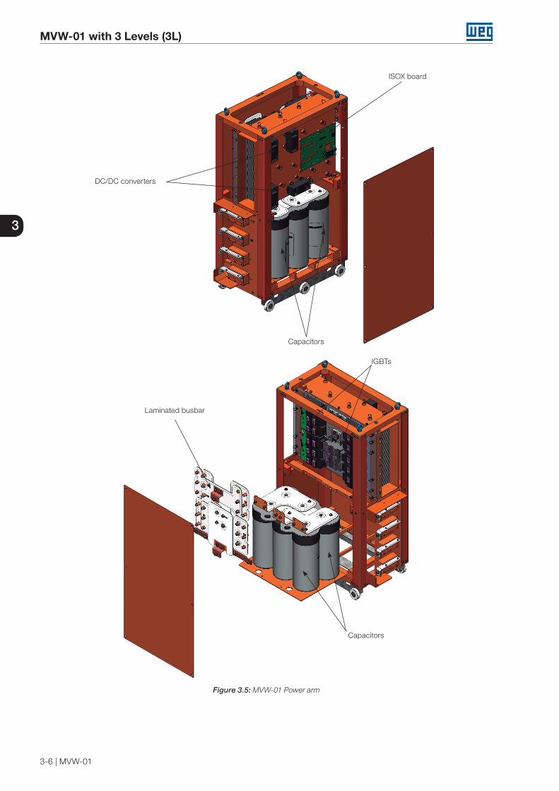
MVW-01 with 3 Levels (3L)
3-6 | MVW-01
3
Capacitors
DC/DC converters
ISOX board
Laminated busbar
IGBTs
Capacitors
Figure 3.5: MVW-01 Power arm
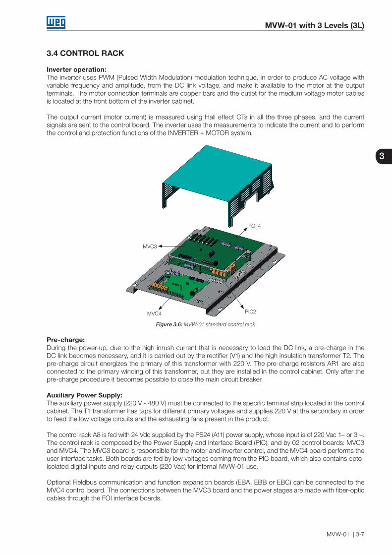
MVW-01 with 3 Levels (3L)
MVW-01 | 3-7
3
3.4 CONTROL RACK
Inverter operation:The inverter uses PWM (Pulsed Width Modulation) modulation technique, in order to produce AC voltage with variable frequency and amplitude, from the DC link voltage, and make it available to the motor at the output terminals. The motor connection terminals are copper bars and the outlet for the medium voltage motor cables is located at the front bottom of the inverter cabinet.
The output current (motor current) is measured using Hall effect CTs in all the three phases, and the current signals are sent to the control board. The inverter uses the measurements to indicate the current and to perform the control and protection functions of the INVERTER + MOTOR system.
FOI 4
PIC2MVC4
MVC3
Figure 3.6: MVW-01 standard control rack
Pre-charge:During the power-up, due to the high inrush current that is necessary to load the DC link, a pre-charge in the DC link becomes necessary, and it is carried out by the rectifier (V1) and the high insulation transformer T2. The pre-charge circuit energizes the primary of this transformer with 220 V. The pre-charge resistors AR1 are also connected to the primary winding of this transformer, but they are installed in the control cabinet. Only after the pre-charge procedure it becomes possible to close the main circuit breaker.
Auxiliary Power Supply:The auxiliary power supply (220 V - 480 V) must be connected to the specific terminal strip located in the controlcabinet. The T1 transformer has taps for different primary voltages and supplies 220 V at the secondary in orderto feed the low voltage circuits and the exhausting fans present in the product.
The control rack A8 is fed with 24 Vdc supplied by the PS24 (A11) power supply, whose input is of 220 Vac 1~ or 3 ~. The control rack is composed by the Power Supply and Interface Board (PIC); and by 02 control boards: MVC3 and MVC4. The MVC3 board is responsible for the motor and inverter control, and the MVC4 board performs the user interface tasks. Both boards are fed by low voltages coming from the PIC board, which also contains opto-isolated digital inputs and relay outputs (220 Vac) for internal MVW-01 use.
Optional Fieldbus communication and function expansion boards (EBA, EBB or EBC) can be connected to the MVC4 control board. The connections between the MVC3 board and the power stages are made with fiber-optic cables through the FOI interface boards.
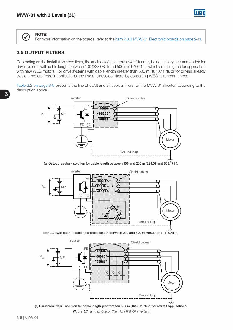
MVW-01 with 3 Levels (3L)
3-8 | MVW-01
3
NOTE!For more information on the boards, refer to the Item 2.3.3 MVW-01 Electronic boards on page 2-11.
3.5 OUTPUT FILTERS
Depending on the installation conditions, the addition of an output dv/dt filter may be necessary, recommended for drive systems with cable length between 100 (328.08 ft) and 500 m (1640.41 ft), which are designed for application with new WEG motors. For drive systems with cable length greater than 500 m (1640.41 ft), or for driving already existent motors (retrofit applications) the use of sinusoidal filters (by consulting WEG) is recommended.
Table 3.2 on page 3-9 presents the line of dv/dt and sinusoidal filters for the MVW-01 inverter, according to the description above.
Shield cables
Ground loop
PE
PE
L
L
L
PE
Inverter
VDC
Motor
MP
(a) Output reactor - solution for cable length between 100 and 200 m (328.08 and 656.17 ft).
PE
Inverter
PE
L
L
L
C
R
R
RC
C
PE
VDC
Ground loop
Motor
Shield cables
MP
(b) RLC dv/dt filter - solution for cable length between 200 and 500 m (656.17 and 1640.41 ft).
PE
MP
Inverter
PE
L
L
L
C C C
PE
VDC
Ground loop
Motor
Shield cables
(c) Sinusoidal filter - solution for cable length greater than 500 m (1640.41 ft), or for retrofit applications.
Figure 3.7: (a) to (c) Output filters for MVW-01 inverters
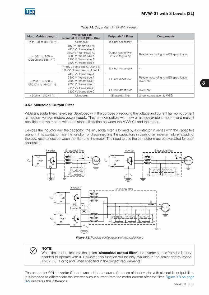
MVW-01 with 3 Levels (3L)
MVW-01 | 3-9
3
Table 3.2: Output filters for MVW-01 inverters
Motor Cables Length Inverter Model:Nominal Current (CT) / Size Output dv/dt Filter Components
Up to 100 m (328.08 ft) All models It is not necessary -
> 100 m to 200 m(328.08 and 656.17 ft)
4160 V / frame size A04160 V / frame size A
3300 V / frame size A03300 V / frame size A2300 V / frame size A2300 V / frame size B
Output reactor with2 % voltage drop
Reactor according to WEG specification
4160V / frame size C, D and E3300V / frame size C, D and E
It is not necessary -
> 200 m to 500 m(656.17 and 1640.41 ft)
4160 V / frame size A3300 V / frame size A2300 V / frame size A2300 V / frame size B
RLC 01 dV/dt filterReactor according to WEG specification RC01 set
4160 V / frame size C3300 V / frame size C
RLC 02 dV/dt filter RC02 set
> 500 m (1640.41 ft) All models Sinusoidal filter Under consultation to WEG
3.5.1 Sinusoidal Output Filter
WEG sinusoidal filters have been developed with the purpose of reducing the voltage and current harmonic contentat medium voltage motors power supply. They are compatible with new or already existent motors, and make it possible to drive motors without distance limitation between the MVW-01 and the motor.
Besides the inductor and the capacitor, the sinusoidal filter is formed by a contactor in series with the capacitive branch. This contactor has the function of disconnecting the capacitors in case of an inverter failure, avoiding, thereby, resonances between the filter and the motor. The need to use the contactor must be evaluated for each application.
MP
Inverter
PEC
LLL
C C
IM
VDC Motor
Sinusoidal filter
MP
Inverter
PEC1
LLL
C1 C1 C2C2 C2
IM
VDC Motor
Sinusoidal filter
MP
MP
Inverter A
Inverter BPE
C1
L1L1L1
L2L2L2
C1 C1 C2C2 C2 C3 C3
IM
C3
PE
VDC
VDC
Motor
Sinusoidal filter
Figure 3.8: Possible configurations of sinusoidal filters
NOTE!When the product features the option “sinusoidal output filter”, the inverter comes from the factory enabled to operate with it. However, this function will be only available in the scalar control mode (P202 = 0, 1 or 2) and when specified in the project requirements.
The parameter P011, Inverter Current was added because of the use of the inverter with sinusoidal output filter. It is intended to differentiate the inverter output current from the motor current after the filter. Figure 3.8 on page 3-9 illustrates this difference.

MVW-01 with 3 Levels (3L)
3-10 | MVW-01
3
Besides the creation of P011, parameters P003 and P400 were changed in order to adapt the use of the MVW-01 with sinusoidal output filter. The description of these parameters can be found in Chapter 11 DETAILED PARAMETER DESCRIPTION on page 11-1.
3.6 AVAILABLE MODELS
Refer to the Table 2.1 on page 2-4 and the Table 2.3 on page 2-6.
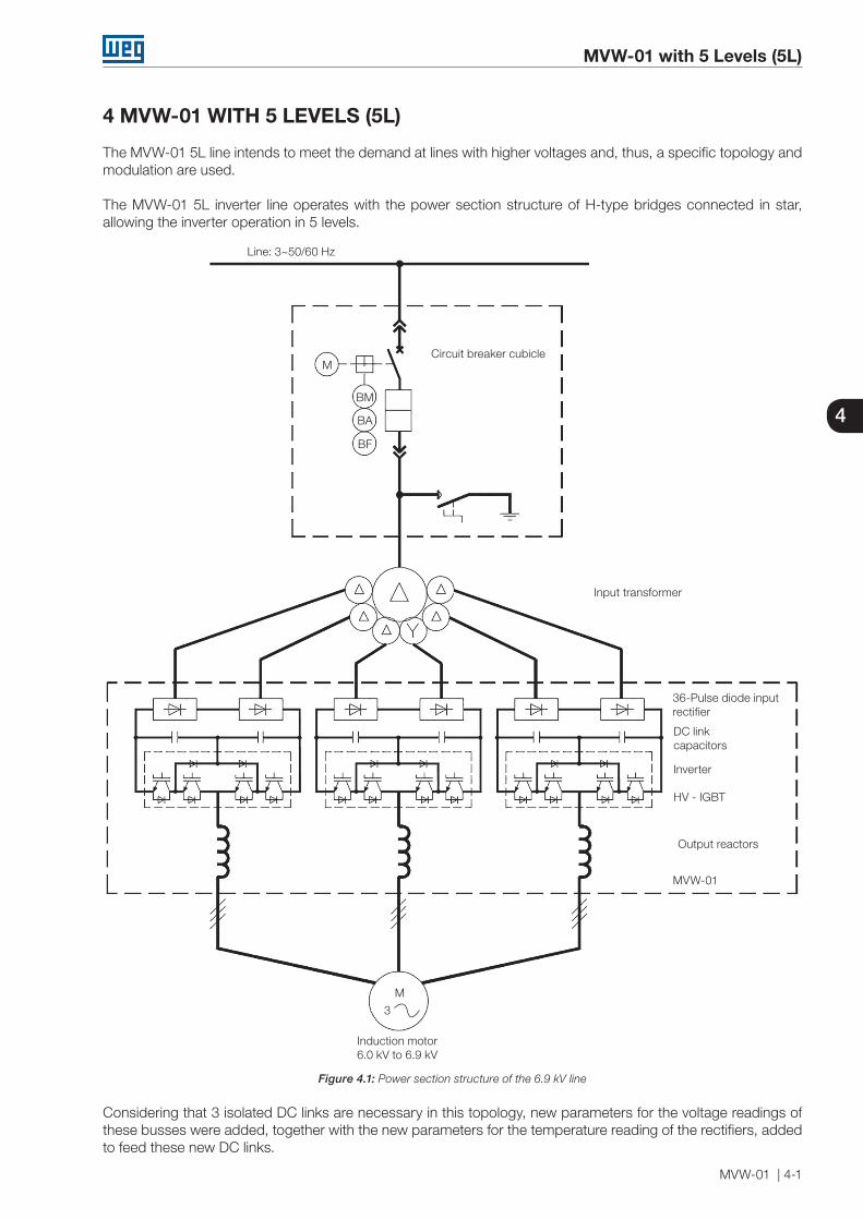
MVW-01 with 5 Levels (5L)
MVW-01 | 4-1
4
4 MVW-01 WITH 5 LEVELS (5L)
The MVW-01 5L line intends to meet the demand at lines with higher voltages and, thus, a specific topology and modulation are used.
The MVW-01 5L inverter line operates with the power section structure of H-type bridges connected in star, allowing the inverter operation in 5 levels.
Line: 3~50/60 Hz
Circuit breaker cubicleM
M
3
BM
BA
BF
Input transformer
36-Pulse diode inputrectifier
DC link capacitors
Output reactors
Inverter
HV - IGBT
MVW-01
Induction motor6.0 kV to 6.9 kV
Figure 4.1: Power section structure of the 6.9 kV line
Considering that 3 isolated DC links are necessary in this topology, new parameters for the voltage readings of these busses were added, together with the new parameters for the temperature reading of the rectifiers, added to feed these new DC links.
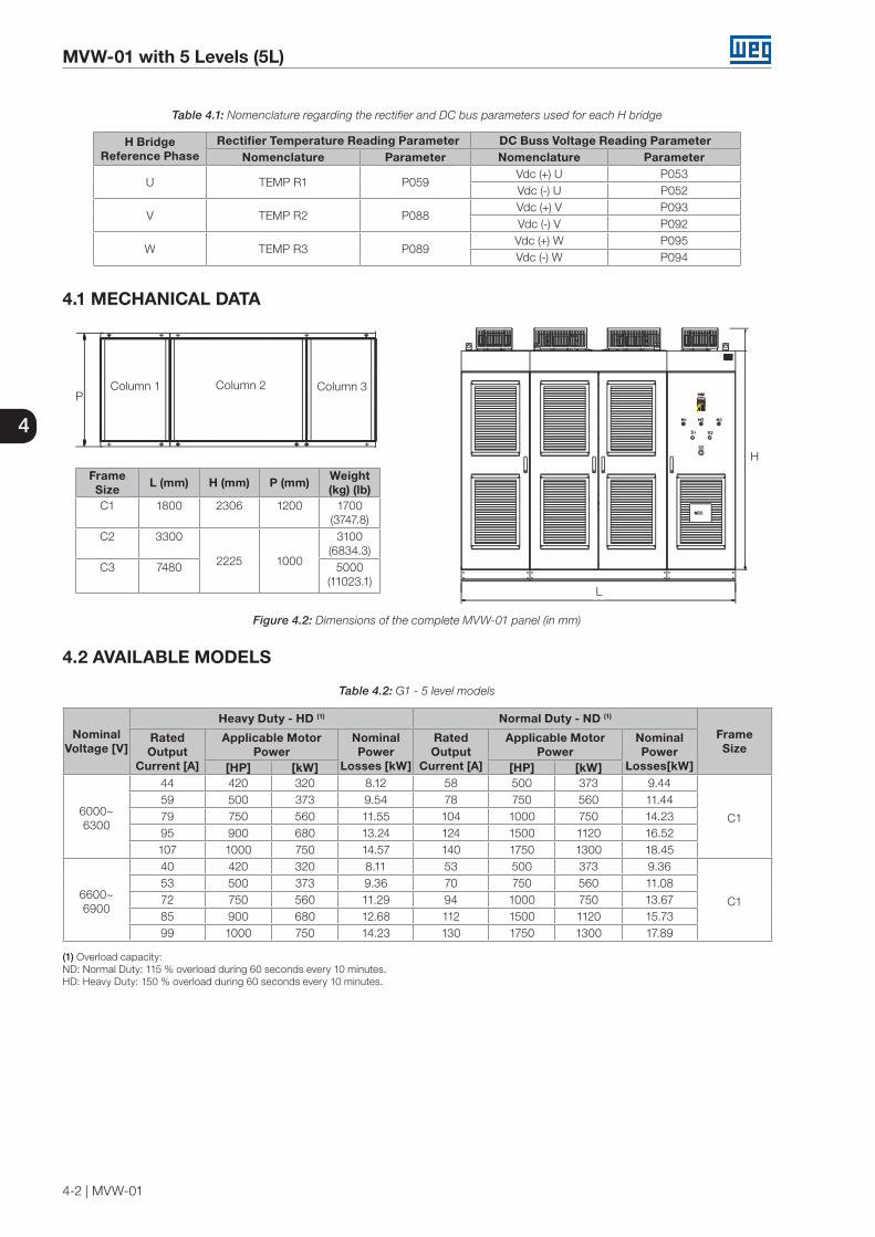
MVW-01 with 5 Levels (5L)
4-2 | MVW-01
4
Table 4.1: Nomenclature regarding the rectifier and DC bus parameters used for each H bridge
H Bridge Reference Phase
Rectifier Temperature Reading Parameter DC Buss Voltage Reading ParameterNomenclature Parameter Nomenclature Parameter
U TEMP R1 P059Vdc (+) U P053Vdc (-) U P052
V TEMP R2 P088Vdc (+) V P093Vdc (-) V P092
W TEMP R3 P089Vdc (+) W P095Vdc (-) W P094
4.1 MECHANICAL DATA
Column 1 Column 2 Column 3P
H
L
FrameSize L (mm) H (mm) P (mm) Weight
(kg) (lb)C1 1800 2306 1200 1700
(3747.8)C2 3300
2225 1000
3100 (6834.3)
C3 7480 5000(11023.1)
Figure 4.2: Dimensions of the complete MVW-01 panel (in mm)
4.2 AVAILABLE MODELS
Table 4.2: G1 - 5 level models
NominalVoltage [V]
Heavy Duty - HD (1) Normal Duty - ND (1)
FrameSize
RatedOutput
Current [A]
Applicable MotorPower
NominalPower
Losses [kW]
RatedOutput
Current [A]
Applicable MotorPower
NominalPower
Losses[kW][HP] [kW] [HP] [kW]
6000~6300
44 420 320 8.12 58 500 373 9.44
C1
59 500 373 9.54 78 750 560 11.4479 750 560 11.55 104 1000 750 14.2395 900 680 13.24 124 1500 1120 16.52107 1000 750 14.57 140 1750 1300 18.45
6600~6900
40 420 320 8.11 53 500 373 9.36
C1
53 500 373 9.36 70 750 560 11.0872 750 560 11.29 94 1000 750 13.6785 900 680 12.68 112 1500 1120 15.7399 1000 750 14.23 130 1750 1300 17.89
(1) Overload capacity:ND: Normal Duty: 115 % overload during 60 seconds every 10 minutes.HD: Heavy Duty: 150 % overload during 60 seconds every 10 minutes.

MVW-01 with 5 Levels (5L)
MVW-01 | 4-3
4
Table 4.3: G2 - 5 level models
NominalVoltage
[V]
Heavy Duty - HD (1) Normal Duty - ND (1) Maximum Current - MX (1)
FrameSize
RatedOutputCurrent
[A]
ApplicableMotorPower
NominalPowerLosses
[kW]
RatedOutputCurrent
[A]
Applicable Motor Power
NominalPowerLosses
[kW]
RatedOutputCurrent
[A]
ApplicableMotorPower
NominalPowerLosses
[kW][HP] [kW] [HP] [kW] [HP] [kW]
6000~6300
55 600 450 9.19 58 700 500 9.43 62 700 500 9.43
C1
69 750 560 10.28 73 800 630 10.60 78 800 630 10.6086 900 710 11.65 91 1000 800 12.07 97 1000 800 12.07108 1250 900 13.49 114 1350 1000 14.01 122 1350 1000 14.01136 1500 1250 15.95 144 1750 1250 16.68 154 1750 1250 16.68170 2000 1400 19.11 180 2250 1600 20.07 181 2250 1600 20.07198 2250 1800 16.63 212 2500 1900 20.64 228 2500 1900 21.82
C2
230 2750 2000 21.97 251 3000 2250 23.54 269 3000 2250 24.92267 3000 2250 24.77 295 3500 2700 26.96 317 3500 2700 28.72310 3700 2800 28.16 348 4000 3150 31.27 373 4000 3150 33.38360 4000 3150 32.28 410 4750 3750 36.59 440 4750 3750 39.27423 4500 3750 38.45 481 5500 4300 43.96 516 5500 4300 47.43
C3496 6000 4500 45.43 565 7000 5000 52.45 606 7000 5000 56.81583 7000 5000 54.35 664 7500 6000 63.23 713 7500 6000 68.87684 8000 6000 65.51 779 9000 7100 76.79 836 9000 7100 83.94
6600~6900
50 600 450 9.52 54 700 500 9.85 58 700 500 9.85
C1
63 750 560 10.60 67 800 630 10.93 72 800 630 10.9381 900 710 12.13 86 1000 800 12.57 92 1000 800 12.57102 1250 900 13.99 109 1350 1000 14.63 117 1350 1000 14.63130 1750 1250 16.58 139 1750 1250 17.44 149 1750 1250 17.44165 2250 1600 20.01 177 2250 1600 21.23 178 2250 1600 21.23192 2500 1900 20.14 205 2750 2000 21.11 221 2750 2000 22.31
C2
223 3000 2200 22.46 241 3000 2250 23.84 260 3000 2250 25.32259 3500 2500 25.24 283 3700 2800 27.15 305 3700 2800 28.95301 3750 2800 28.62 332 4000 3150 31.20 358 4000 3150 33.41350 4500 3550 32.73 390 4750 3550 36.22 420 4750 3550 38.92411 5000 4000 38.77 458 6000 4500 43.26 494 6000 4500 46.84
C3482 6500 4750 45.63 538 7250 5000 51.35 580 7250 5000 55.82566 7500 5600 54.31 631 8000 6300 61.44 680 8000 6300 67.05665 8000 6500 65.31 740 9500 7400 74.20 798 9500 7400 81.41
(1) Overload capacity:MX: Maximum Current: overload is not allowed.ND: Normal Duty: 115 % overload during 60 seconds every 10 minutes.HD: Heavy Duty: 150 % overload during 60 seconds every 10 minutes.
(2) The motor powers are only illustrative and the correct inverter selection must be done in function of the rated current of the motor to be used, as well as the overloads related to the application.The rated input currents are equal or less than the rated output currents.The maximum output currents are allowed during 60 seconds every 10 minutes.

MVW-01 with 5 Levels (5L)
4-4 | MVW-01
4

MVW-01C (Compact)
MVW-01 | 5-1
5
5 MVW-01C (COMPACT)
The line MVW-01C is a variable frequency inverter destined to control medium voltage induction motors with nominal voltages of 2300 V, 3300 V and 4160 V, with a power range from 500 to 1200 HP. It uses non-controlled semiconductors (diodes) at the input rectifier stage and controlled semiconductors (HV-IGBTs) to generate the three output phases at the inverter stage, in order to control the medium voltage motor speed and torque.
The MVW-01C inverter line uses the same topology as the MVW-01 line and has as the main feature compact dimensions. In order to achieve such dimensional reduction, all the inverter components are scaled to the power range of this product line. Another feature of this line is that in its standard version the inverter uses an 18 pulse rectifier bridge, which demands a special transformer with 3 secondary windings and 20° phase shift among them.
The MVW-01C presents protections against overload, short-circuit, phase loss, undervoltage, overvoltage, overtemperature, and ground fault, it also has an independent fault monitoring for each HV-IGBT, has pressure sensors for ventilation efficiency monitoring, and presents output current limitation. The control type can be selected by the user, between scalar control (constant V/f ratio) and vector control (with sensorless or encoder feedback).
Line voltage until 22 kV 3~50/60 Hz
Input cubicle
Input transformer
Rectifier input diode(12, 18 or 24 pulse)
Compact medium voltage frequencyinverter
Multilevel NPC inverter (3/5 levels) HV-IGBT
DC link capacitors
Main circuit breakeror contactor
M 3 ~
Figure 5.1: General block diagram

MVW-01C (Compact)
5-2 | MVW-01
5
Figure 5.2: MVW-01C panel
Transformer
An isolating transformer is required to provide the number of secondary windings necessary to the rectifier bridge and the appropriate voltage level. The minimum specifications of the input transformer are:
Nominal power according to the inverter power rating considering the input current harmonics.
Minimum impedance of 6 %.
Shield between primary and secondary windings.
Primary voltage according to the available line voltage.
Secondary voltages according to the motor nominal voltage and 7.2 kV voltage insulation class.
Input Rectifier
The medium voltage cables for the input rectifier (A1) supply come from the input transformer secondary windings.The transformer configuration and the number of cables depend on the rectifier number of pulses:
6 cables for the 12 pulse configuration.
9 cables for the 18 pulse configuration.
12 cables for the 24 pulse configuration.
Considering the standard rectifier version (18 pulses) the secondary winding voltage depends on the motor nominal voltage, being 1.5 kV for motors with 4160 V rated voltage and 1.2 kV for motors with 3300 V rated voltage. The 9 cables may be inserted through the bottom part of the rectifier cabinet or through the top of the inverter cabinet,
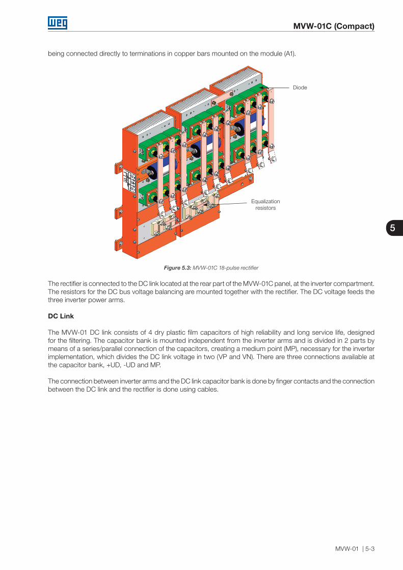
MVW-01C (Compact)
MVW-01 | 5-3
5
being connected directly to terminations in copper bars mounted on the module (A1).
Diode
Equalizationresistors
Figure 5.3: MVW-01C 18-pulse rectifier
The rectifier is connected to the DC link located at the rear part of the MVW-01C panel, at the inverter compartment. The resistors for the DC bus voltage balancing are mounted together with the rectifier. The DC voltage feeds the three inverter power arms.
DC Link
The MVW-01 DC link consists of 4 dry plastic film capacitors of high reliability and long service life, designed for the filtering. The capacitor bank is mounted independent from the inverter arms and is divided in 2 parts by means of a series/parallel connection of the capacitors, creating a medium point (MP), necessary for the inverter implementation, which divides the DC link voltage in two (VP and VN). There are three connections available at the capacitor bank, +UD, -UD and MP.
The connection between inverter arms and the DC link capacitor bank is done by finger contacts and the connection between the DC link and the rectifier is done using cables.
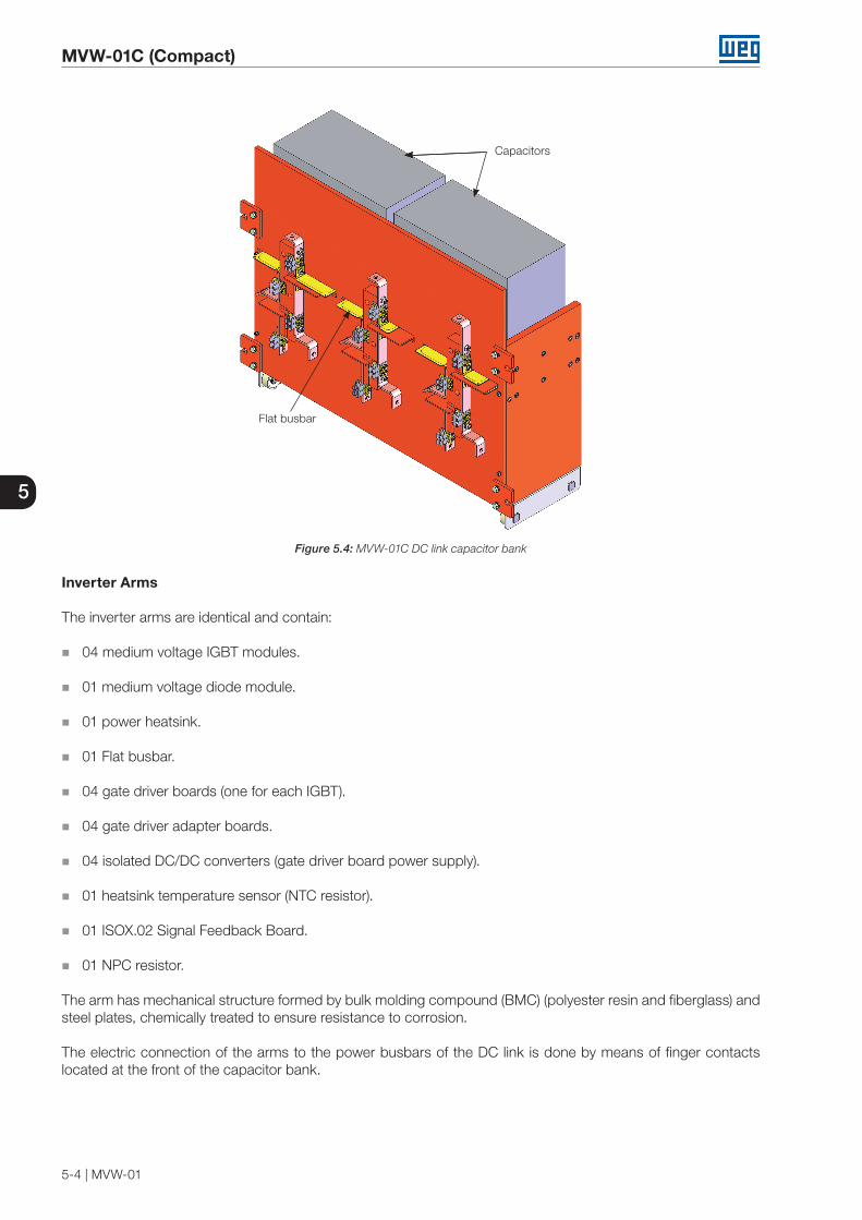
MVW-01C (Compact)
5-4 | MVW-01
5
Flat busbar
Capacitors
Figure 5.4: MVW-01C DC link capacitor bank
Inverter Arms
The inverter arms are identical and contain:
04 medium voltage IGBT modules.
01 medium voltage diode module.
01 power heatsink.
01 Flat busbar.
04 gate driver boards (one for each IGBT).
04 gate driver adapter boards.
04 isolated DC/DC converters (gate driver board power supply).
01 heatsink temperature sensor (NTC resistor).
01 ISOX.02 Signal Feedback Board.
01 NPC resistor.
The arm has mechanical structure formed by bulk molding compound (BMC) (polyester resin and fiberglass) and steel plates, chemically treated to ensure resistance to corrosion.
The electric connection of the arms to the power busbars of the DC link is done by means of finger contacts located at the front of the capacitor bank.

MVW-01C (Compact)
MVW-01 | 5-5
5
Connection bars
Figure 5.5: MVW-01C power arm
DC/DCconverters
IGBTs
Heatsink
Flat busbarISOX board
Figure 5.6: MVW-01C Power arm
Control rack
The control rack used in the MVW-01C inverter line has the same functions and uses the same boards of the rack used in the MVW-01 3L line. Refer to the Section 3.4 CONTROL RACK on page 3-7 for the description of the functions, control rack and optional boards.
It is observed only a change in the arrangement of the boards because of the need for compaction of the MVW-01C line.

MVW-01C (Compact)
5-6 | MVW-01
5
MVC4
MVC3
PIC2
FOI4
Figure 5.7: MVW-01C control rack
5.1 PANEL CONSTRUCTIVE DETAILS
The MVW-01C is supplied in form of a panel with the dimensions: 1000 mm x 2312 mm x 980 mm (width x height x depth). The complete panel can be defined, according to the components mounted in each panel division and to their functions, as the union of three compartments:
Rectifier Compartment.
Inverter Compartment.
Control Compartment.
The Figure 5.8 on page 5-6 shows the complete panel drawing. The inverter arms are supplied separately in proper packages.
Arm dimensions: 260 mm x 607 mm x 522 mm (width x height x depth).
1000
95
575
250
1140
2000
2320
001
1000500 500
H1
S2 S1 S3
H2 H3
Figure 5.8: Dimensions of the MVW-01C panel

MVW-01C (Compact)
MVW-01 | 5-7
5
The internal component distribution is presented in the Figure 5.9 on page 5-7.
H3
S5
K1
K3
K4
KA1
KA
2
X8U V W
X9 X10 X12
010
01 02 03 05 06 07 08 0901
101
2
S1 S2
H2 H1
Rear view ofthe LV door
Control compartment
Rectifier compartment
Input busbars
Output busbars
Inverter compartment
BIR BIS BIT
Figure 5.9: MVW-01C internal component arrangement
5.2 AVAILABLE MODELS
Table 5.1: MVW-01C - G1 models
NominalVoltage
[V]
Heavy Duty - HD (1) Normal Duty - ND (1)
RatedOutputCurrent
[A]
Applicable Motor Power NominalPowerLosses
[kW]
RatedOutputCurrent
[A]
Applicable Motor Power NominalPowerLosses
[kW][HP] [kW] [HP] [kW]
2300
85 380 280 3.54 97 430 320 4.10100 440 330 4.24 112 500 370 4.82112 490 373 4.82 125 550 420 5.49125 550 416 5.49 138 600 450 6.17
3300
85 500 400 4.71 97 600 450 5.14100 600 450 5.14 112 700 500 5.51112 700 500 5.51 128 800 630 6.36125 750 560 5.95 138 850 670 6.61
4160
70 500 400 5.14 80 600 450 5.4380 600 450 5.43 91 700 500 5.8594 700 500 5.85 110 800 630 6.38110 800 630 6.38 120 900 710 6.72120 900 710 6.72 130 1000 800 7.07
(1) Capacity:ND: Normal Duty: 115 % overload during 60 seconds every 10 minutesHD: Heavy Duty: 150 % overload during 60 seconds every 10 minutes.
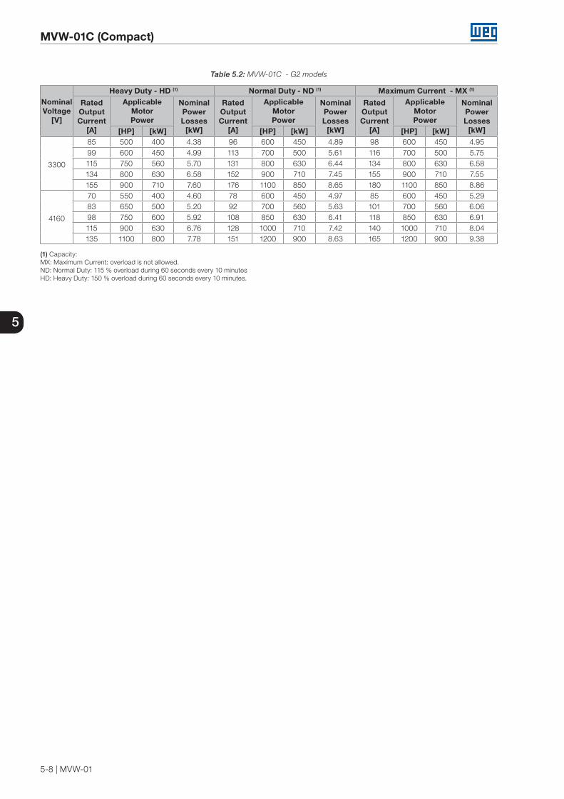
MVW-01C (Compact)
5-8 | MVW-01
5
Table 5.2: MVW-01C - G2 models
NominalVoltage
[V]
Heavy Duty - HD (1) Normal Duty - ND (1) Maximum Current - MX (1)
RatedOutputCurrent
[A]
Applicable MotorPower
NominalPowerLosses
[kW]
RatedOutputCurrent
[A]
Applicable MotorPower
NominalPowerLosses
[kW]
RatedOutputCurrent
[A]
Applicable MotorPower
NominalPowerLosses
[kW][HP] [kW] [HP] [kW] [HP] [kW]
3300
85 500 400 4.38 96 600 450 4.89 98 600 450 4.9599 600 450 4.99 113 700 500 5.61 116 700 500 5.75115 750 560 5.70 131 800 630 6.44 134 800 630 6.58134 800 630 6.58 152 900 710 7.45 155 900 710 7.55155 900 710 7.60 176 1100 850 8.65 180 1100 850 8.86
4160
70 550 400 4.60 78 600 450 4.97 85 600 450 5.2983 650 500 5.20 92 700 560 5.63 101 700 560 6.0698 750 600 5.92 108 850 630 6.41 118 850 630 6.91115 900 630 6.76 128 1000 710 7.42 140 1000 710 8.04135 1100 800 7.78 151 1200 900 8.63 165 1200 900 9.38
(1) Capacity:MX: Maximum Current: overload is not allowed.ND: Normal Duty: 115 % overload during 60 seconds every 10 minutesHD: Heavy Duty: 150 % overload during 60 seconds every 10 minutes.
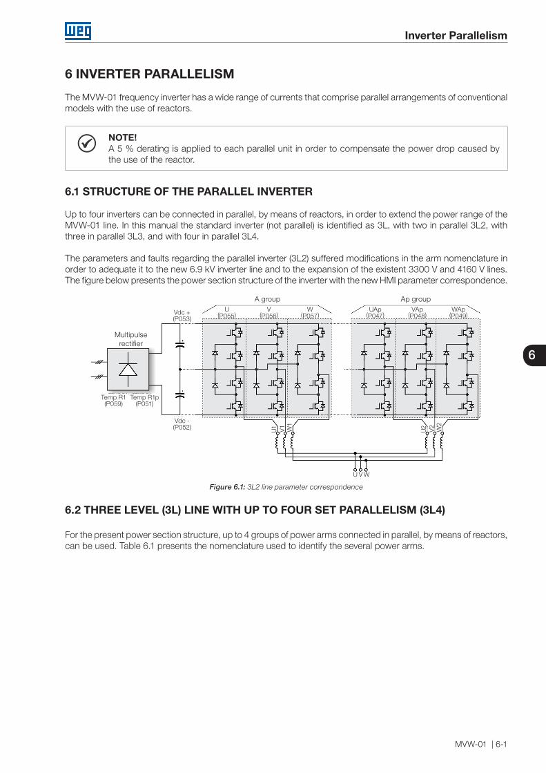
Inverter Parallelism
MVW-01 | 6-1
6
6 INVERTER PARALLELISM
The MVW-01 frequency inverter has a wide range of currents that comprise parallel arrangements of conventionalmodels with the use of reactors.
NOTE!A 5 % derating is applied to each parallel unit in order to compensate the power drop caused by the use of the reactor.
6.1 STRUCTURE OF THE PARALLEL INVERTER
Up to four inverters can be connected in parallel, by means of reactors, in order to extend the power range of the MVW-01 line. In this manual the standard inverter (not parallel) is identified as 3L, with two in parallel 3L2, with three in parallel 3L3, and with four in parallel 3L4.
The parameters and faults regarding the parallel inverter (3L2) suffered modifications in the arm nomenclature in order to adequate it to the new 6.9 kV inverter line and to the expansion of the existent 3300 V and 4160 V lines. The figure below presents the power section structure of the inverter with the new HMI parameter correspondence.
Multipulserectifier
A group
Vdc + (P053)
Vdc - (P052)
Temp R1 (P059)
Temp R1p (P051)
U (P055)
UAp (P047)
V (P056)
VAp (P048)
W (P057)
WAp (P049)
Ap group
U V W
U1
U2V1 V2W1
W2
Figure 6.1: 3L2 line parameter correspondence
6.2 THREE LEVEL (3L) LINE WITH UP TO FOUR SET PARALLELISM (3L4)
For the present power section structure, up to 4 groups of power arms connected in parallel, by means of reactors, can be used. Table 6.1 presents the nomenclature used to identify the several power arms.
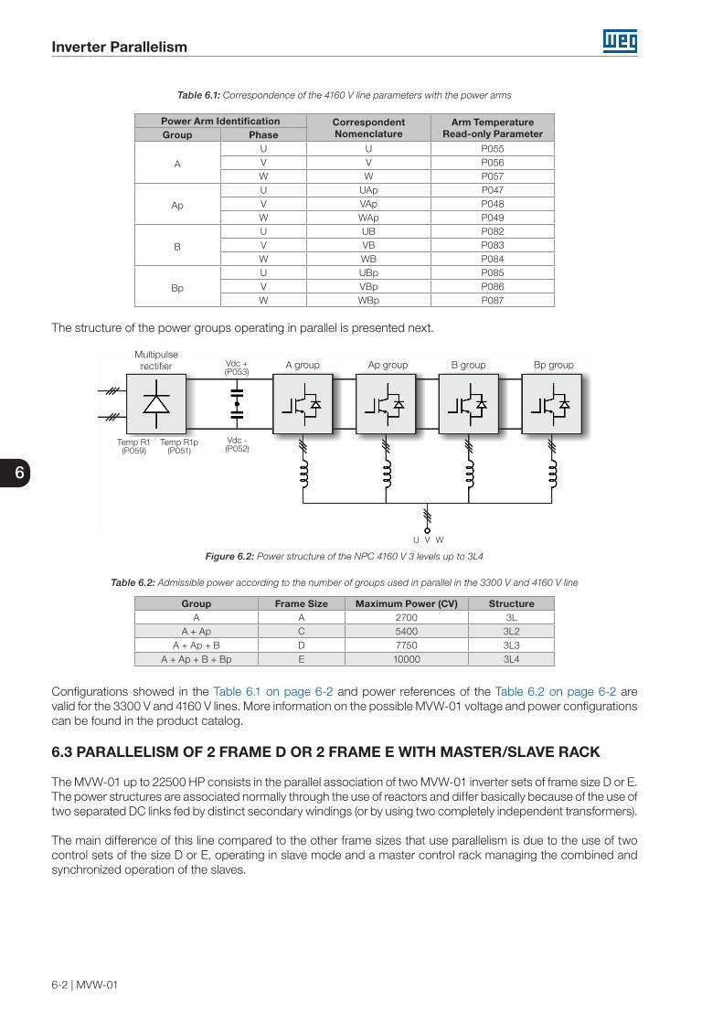
Inverter Parallelism
6-2 | MVW-01
6
Table 6.1: Correspondence of the 4160 V line parameters with the power arms
Power Arm Identification CorrespondentNomenclature
Arm Temperature Read-only ParameterGroup Phase
A
U U P055V V P056W W P057
Ap
U UAp P047V VAp P048W WAp P049
B
U UB P082V VB P083W WB P084
Bp
U UBp P085V VBp P086W WBp P087
The structure of the power groups operating in parallel is presented next.
Multipulserectifier A group B groupAp group Bp groupVdc +
(P053)
Vdc - (P052)
Temp R1 (P059)
Temp R1p (P051)
U V W
Figure 6.2: Power structure of the NPC 4160 V 3 levels up to 3L4
Table 6.2: Admissible power according to the number of groups used in parallel in the 3300 V and 4160 V line
Group Frame Size Maximum Power (CV) StructureA A 2700 3L
A + Ap C 5400 3L2A + Ap + B D 7750 3L3
A + Ap + B + Bp E 10000 3L4
Configurations showed in the Table 6.1 on page 6-2 and power references of the Table 6.2 on page 6-2 are valid for the 3300 V and 4160 V lines. More information on the possible MVW-01 voltage and power configurations can be found in the product catalog.
6.3 PARALLELISM OF 2 FRAME D OR 2 FRAME E WITH MASTER/SLAVE RACK
The MVW-01 up to 22500 HP consists in the parallel association of two MVW-01 inverter sets of frame size D or E. The power structures are associated normally through the use of reactors and differ basically because of the use of two separated DC links fed by distinct secondary windings (or by using two completely independent transformers).
The main difference of this line compared to the other frame sizes that use parallelism is due to the use of two control sets of the size D or E, operating in slave mode and a master control rack managing the combined and synchronized operation of the slaves.

Inverter Parallelism
MVW-01 | 6-3
6
Multipulserectifier
DC link
IM
Inverter
Slave
Control
Slave
Master
Inputtransformer
Supply line
Figure 6.3: General diagram for the 2 x D and 2 x E models
This structure is necessary to increase the total number of inverter power arms, and in this system two inverters in parallel can be used, which, with the command of an auxiliary control rack equipped with specific software enables the operation of the system as a whole. The nomenclature regarding the power cell groups was maintained for each slave inverter, just like the parameters and the faults.
The control for the line up to 2 x E presents the need to use 3 HMIs, being one of them for the master rack whereas the two other present information regarding individual readings and faults of the slave racks. Table 6.3 on page 6-3 lists the readings that are exhibited differently in the HMI of the master.
Table 6.3: Parameters exhibited differently in master and slave HMIs
Parameter Slave HMI (standard) Master HMIP003 Inverter Current Addition of the slave inverter currentsP004 DC Link Voltage Highest voltage among the slave DC links
NOTE!The created and changed parameters are presented in Chapter 11 DETAILED PARAMETER DESCRIPTION on page 11-1, the same applies to faults and alarms, which are entirely described in Chapter 14 DIAGNOSTICS AND TROUBLESHOOTING on page 14-1.
The connection between the master/slave commands can be performed according to the diagrams of Figure 6.4 on page 6-3 or Figure 6.5 on page 6-4.
SLAVE 1FOI3
CLK TXTEMP_RV2N1_UA1
N2_UA1
N5_UA1
N6_UA1
N1_VA1
N2_VA1
N5_VA1
N6_VA1
N1_WA1
N2_WA1
TEMP_RV2
TEMP_RW2
ARC8
ARC8
NDO1
NDO1
NDO2
NDO2
CLK TX
CLK RX
CLK RX
TX DATA
TX DATA
RX DATA
RX DATA
LOAD
LOAD
MASTER FOI3
SLAVE 2FOI3
TEMP_RW2
Figure 6.4: Communication between master and slave racks using FOI3

Inverter Parallelism
6-4 | MVW-01
6
SLAVE 1FOI3
MASTER FOI4
SLAVE 2FOI3
CLK TXTEMP_RV2N1_U
N2_U
N5_U
N6_U
N1_V
N2_V
N5_V
N6_V
N1_W
N2_W
TEMP_RV2
TEMP_RW2
ARC8
ARC8
NDO1
NDO1
NDO2
NDO2
CLK TX
CLK RX
CLK RX
TX DATA
TX DATA
RX DATA
RX DATA
LOAD
LOADTEMP_RW2
Figure 6.5: Communication between master and slave racks using FOI4
NOTE!The connections are made with fiber optic cables, with a length limit of 10 m. More information on panel connections and mechanical dimensions can be found in the inverter electrical project.
6.4 FIVE LEVEL (5L) PARALLELISM LINE
For the higher power inverters of the 6.9 kV line, it is necessary the use of parallel H bridges per phase and, in the same way as for the 4160 V, the parallelism occurs by the use of reactors. Figure 6.6 on page 6-5 shows the detailed description of the H bridge topology, as well as the related parameters.

Inverter Parallelism
MVW-01 | 6-5
6
Multipulserectifier
Multipulserectifier
Multipulserectifier
Vdc (+) U (P053)
Vdc (+) V (P093)
Vdc (+) W (P095)
Vdc (-) U (P052)
Vdc (-) V (P092)
Vdc (-) W (P094)
Temp R1 (P059)
Temp R2 (P088)
Temp R3 (P089)
U (P055)
V (P056)
W (P057)
U UAp
V VAp
W WAp
+
+
+
+
+
+
UB (P082)
VB (P083)
WB (P084)
UAp (P047)
VAp (P048)
WAp (P049)
UBp (P085)
VBp (P086)
WBp (P087)
UBpUB
VBpVB
WBpWB
Figure 6.6: Topology of the 6.9 kV line 5 levels parallel
The parallelism reactors are magnetically coupled, as shown in the next figure.
UU
V
W
UB
UAp UBp
V VB
VAp VBp
W WB
WAp WBp
Figure 6.7: Parallelism reactors connectionof the 6.9 kV line
The other mechanical and power options of the 6.9 kV line can be found in the product catalog.

Inverter Parallelism
6-6 | MVW-01
6
The parameters and faults correspondent to the power structure of this line are described in Chapter 11 DETAILED PARAMETER DESCRIPTION on page 11-1 and Chapter 14 DIAGNOSTICS AND TROUBLESHOOTING on page 14-1.

Synchronous Motor Line
MVW-01 | 7-1
7
7 SYNCHRONOUS MOTOR LINE
In order to allow driving synchronous motors, the MVW-01 introduces a number of software functions and new hardware elements for commanding and controlling these motors.
Figure 7.1 on page 7-1 presents the general diagram for driving the synchronous motor using the MVW-01. For more details on the Excitation Control System and the direct connection of the motor to the line, refer to the electrical project of the inverter.
Supply line
Auxiliary line
E
Y Y
- +
SM
Interlocked
AC/DC converter
Excitationcontrolsystem
Crowbar
MVW-01
MVC3
MVC4
RSSI
Figure 7.1: General diagram of the inverter for synchronous motor
7.1 ABSOLUTE ENCODER WITH RSSI BOARD
In the application of driving synchronous machines, it is necessary to make sure that the inverter has the exact position of the rotor regarding the stator and, since the incremental encoder is not capable of supplying this information, the use of an absolute encoder becomes necessary.
7.1.1 Absolute Encoder
The synchronous motor control requires the use of an absolute encoder, which must follow the following specifications:
Synchronous Serial Interface (SSI) communication protocol with RS-485 communication channel, with clock and16 bit word size in the following format:14 data bits1 ZERO bit1 even parity bit

Synchronous Motor Line
7-2 | MVW-01
7
Clock
Data
MSB
BIT 13 BIT 12 BIT 11 BIT 0 Zero Par.
LSB Zero Parity
t1 T
nT
t2
Figure 7.2: Clock specification and data transfer for the absolute encoder
Supply voltage of 15 V, with consumption lower than 300 mA;
Resolution of 14 bits per turn, which ensures a dynamic equivalent to the conventional incremental encoder;
When mounting the encoder next to the motor, it is recommended:Coupling the encoder directly to the motor shaft (using a flexible coupling, however without torsional flexibility);Both the shaft and the metallic frame of the encoder must be electrically isolated from the motor (minimum distance of 3 mm);
Use good quality flexible couplings that prevent mechanical oscillations or "backlash".
NOTE!The standard absolute encoder recommended for the MVW-01 is the Baumer MHAP 400 B5 XXXXSB14EZ D.The maximum encoder cable length is 120 m.Refer to the motor project to define the type of encoder mounting.
7.1.2 RSSI Board
The use of absolute encoder implies the need for an SSI data interface (Synchronous Serial Interface) between the encoder and the inverter. The RSSI board was developed for the encoder specification previously described.This board has the following features:
Supply voltage of 24 V DC, with consumption of up to 700 mA;RS485 communication channel for data transmission and clock according to SSI standard with absolute encoder;2 fiber optic communication channels for use with up to two boards, MVC3 control and FOI3.
Use shielded cable for the electrical connection, keeping it as far as possible (> 25 cm) from the other wiring (power, control, etc.). Preferably, inside a metallic conduit.
Encoder Conector
CLK + CLK +3
DATA + DATA +8
DATA - DATA -7
DGND DGND6
6 9
51
Shield Shield Ground
Reference
Power supply
Absolute
Encoder
Signals
DescriptionRSSI-XC2 Connector
MVW-01 RSSIboard
XC2 connector(DB9 - Male)
5Shield
Brown
White
Pink
Gray
Blue
Red
Vdc Vdc4
CLK - CLK -2
Figure 7.3: RSSI - Encoder connection cable
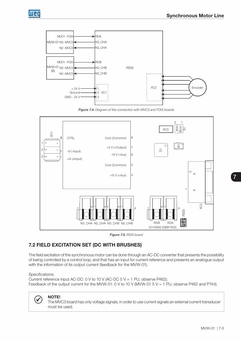
Synchronous Motor Line
MVW-01 | 7-3
7
NDO1 - FOI3 RDA
RDB
N3_CHA
N3_CHB
N2_CHA
N2_CHB
NDO1 - FOI3
N2 - MVC3
N2 - MVC3
+ 24 V 1 Ground 2 XC1
XC2 Encoder
GND - 24 V 3
N3 - MVC3
N3 - MVC3 MVW-01 (B)
RSSI
MVW-01
Figure 7.4: Diagram of the connection with MVC3 and FOI3 boards
1
1
1
2 2
2
1 2
XC1
XC3 ON
12
XC2
RDB RDA
3
33
3
RS
SI
8
7
6
96
5
5
4
444 441 1 4
1
111 1D
1
CTRL Com (Common)
Com (Common)
12119560 (GBR R02)N3_CHA N2_CHA N3_CHB N2_CHB
+5 V (+Output)
-15 V (-Aux)
+15 V (+Aux)
-Vi (-Input)
+Vi (+Input)
B1
S1
Figure 7.5: RSSI board
7.2 FIELD EXCITATION SET (DC WITH BRUSHES)
The field excitation of the synchronous motor can be done through an AC-DC converter that presents the possibility of being controlled by a control loop, and that has an input for current reference and presents an analogue output with the information of its output current (feedback for the MVW-01).
Specifications:Current reference input AC-DC: 0 V to 10 V (AC-DC 5 V = 1 PU, observe P462);Feedback of the output current for the MVW-01: 0 V to 10 V (MVW-01 5 V = 1 PU, observe P462 and P744).
NOTE!The MVC3 board has only voltage signals, in order to use current signals an external current transducer must be used.

Synchronous Motor Line
7-4 | MVW-01
7
An example of how to program the inverter to configure the field current reference is shown in Figure 7.6 on page 7-4, and the parameters mentioned in the image are described in Chapter 11 DETAILED PARAMETER DESCRIPTION on page 11-1.
Field currentreference
P180
|m|P177 P450
P178 P449P175/P176P182/P183
∑ ∑φ
|φ|
+ -
+ -i f*
|m| = modulation index modulusφ = stator flux|φ| = stator flux modulus
i*f = field current reference
Figure 7.6: Parameters used by the inverter in the calculation of the of the field current reference
NOTE!Information presented in Chapter 7 SYNCHRONOUS MOTOR LINE on page 7-1 of this manual refers to the operation of synchronous machines with DC excitation and with brushes. In order to drive synchronous machines with other types of excitation, consult WEG.
Installation, Connection and Energization
MVW-01 | 8-1
8
8 INSTALLATION, CONNECTION AND ENERGIZATION
This chapter describes the electrical and mechanical installation procedures for the MVW-01. The presented guidance and suggestions must be followed in order to assure the proper inverter operation.
ATTENTION! The handling of the MVW-01 and its mechanical and electrical installation must be carried out by
persons trained and qualified by WEG.STORAGE OF THE MVW-01 PANEL AND ARMS:
After receiving the equipment, remove the plastic film in order to prevent moisture condensation. Do not store exposed to sunshine and to temperatures above 40 °C (104 °F). Store the equipment in a clean, protected place with relative humidity not higher than 80 %. During all the storage period the conditions mentioned earlier must be satisfied, but when
components are stored for more than one year, measures must be taken to dehumidify the storage location.
When using equipment after a long storage period, verify whether the equipment is free of scratches, dirt, rust and other damages.
The inverter performance and reliability can be impaired if the inverter or the power arms were stored in an environment out of the conditions listed previously.
DANGER! The procedures recommended in this warning have the purpose of protecting the user from death,
severe personal injury and considerable property damage. Power supply isolating switches: equipment for isolating the inverter power and auxiliary supplies
must be planed. They must cut off the inverter supplies (e.g., during installation maintenance tasks). This equipment cannot be used as emergency stop mechanism. Make sure that the power supply is disconnected before starting the wiring. The following information is intended to be a guide for a proper installation. Comply with applicable
local regulations for electrical installations.
DANGER! Les procédures recommandées dans cet avertissement visent à protéger l’utilisateur de la mort,
de blessures graves et de dégâts matériels importants. Interrupteurs d’isolement de l’alimentation : Le matériel d’isolement de l’alimentation de l’onduleur
et des alimentations auxiliaires doit être prévu. Il doit couper les alimentations de l’onduleur (par ex.: pendant les tâches de maintenance de l’installation).
Cet équipement ne doit pas être utilisé comme mécanisme d’arrêt d’urgence. Vérifiez que l’alimentation est débranchée avant de commencer le câblage. Les informations suivantes ont pour but de servir de guide pour une bonne installation. Respectez
la réglementation locale applicable sur les installations électriques.
8.1 MECHANICAL INSTALLATION
8.1.1 Environmental Conditions
The inverter installation location is an important factor to assure good performance and high product reliability. The inverter must be installed in an environment free of:
Direct exposure to sunlight, rain, high humidity, or sea-air.
Inflammable or corrosive gases or liquids.
Excessive vibration, dust or metallic particles and oil mist.
Installation, Connection and Energization
8-2 | MVW-01
8
Allowed environmental conditions:
Temperature: From 0 ºC to 40 ºC (32 ºF to 140 ºF) - nominal conditions (no derating required).
From 40 ºC to 50 ºC (140 ºF to 122 ºF): current reduction of 2.5 % for each Celsius degree above 40 ºC (140 ºF).
Relative humidity: from 5 % to 90 % non-condensing.
Altitude: up to 1000 m (3.300 ft) - nominal conditions (no derating required).
From 1000 m to 4000 m (3,300 ft to 13.200 ft) - current derating of 1 % each 100 m (or 0.3 % each 100 ft) above 1000 m (3.300 ft) altitude.
Pollution degree: 2 (according to IEC/UL standards) with non-conductive pollution.
Condensation shall not originate conduction through the accumulated residues.
The medium voltage inverter MVW-01 is supplied in form of a panel, whose dimensions are presented in Table 3.1 on page 3-3. According to the components mounted in each column and to their function, this complete panel results in in the inseparable union of three functions, rectifier, inverter and control.
The inverter power arms are supplied separately in their own packing.
Arm dimensions: 360 mm x 1040 mm x 680 mm (width x height x depth).
8.1.2 Handling Recommendations
The inverter package must be removed only at the installation site, where the panel will be operated. Before hoistingor moving the panel, locate the hoisting eyes and fragile spots in the documentation that comes with the product.Follow the instructions that come with the panel.
8.1.3 Hoisting
Make sure that the lifting device used to hoist the panel and the arms is suitable for their weight and shape, referto the Table 8.1 on page 8-2.
Table 8.1: Panel weight (approximately)
Frame Size Weight kg (lb)A0 900A 1560B 1700C 2700D 4500E 5000
2 x D 2 x 45002 x E 2 x 5000
The inverter arms weigh approximately 140 kg (308.6 lb) each arms.
Observe the gravity center and ensure that the hoisting mechanism is adequate and safe. Use the configurationshowed in the Figure 8.1 on page 8-3.
The cables or chains used for hoisting must be at a minimum angle of 45° regarding the horizontal plane.
Hoisting must be done in a slow and stable manner. Before starting make sure the entire pass is clear of obstacles.If any alteration or damage in the panel structure is noticed, then abort the hoisting and rearrange the cables or chains.

Installation, Connection and Energization
MVW-01 | 8-3
8
A
Multiple securingpoints
C ≥ 2400
C
A = Mín. 45º
Figure 8.1: Recommended hoisting mechanism for the panel movement
8.1.4 Moving When cranes or pulleys are used, make sure that the movements are slow and smooth, so that the panel and thearms do not suffer excessive swings and vibration.
When using movable hydraulic jacks, forklifts, rollers or other means, distribute the support points from one extremethrough the other, avoiding pressure on fragile areas.
Make sure that all the panel doors be closed and locked, and that the door handles be in protected position.
8.1.5 Unpacking
Use proper tools to unpack the MVW-01 panel and its arms. During this process, make sure that all the items listed in the documentation that comes with the product are present and in perfect conditions. Contact your local WEG representative in case of any irregularity.
Remove the arm packages carefully. The arms have hoisting eyes.
The inverter arms have fragile components (electronic boards, fiber optic connectors, busbars, wiring, etc.). Avoid touching these components! The arms must always be handled through their external metallic frame. While opening the package, inspect the arms for transportation damage. Do not install the arms if they are damaged or if you suspect of any damage.
Remove all packing material (plastic, wood, polystyrene foam, metal, nails, bolts, nuts, etc.) that might have remained inside the inverter panel or in the arms.
ATTENTION!If any component presents problems (damages) it is recommended to:
Stop the unpacking immediately. Contact the carrier and formally fill in a complaint with the problem found. Take pictures of the damaged parts. Contact your WEG representative or service.

Installation, Connection and Energization
8-4 | MVW-01
8
Pallet
Arm
Wooden package
Strapping
Polystyrene wedge
Figure 8.2: Standard power arm with package

Installation, Connection and Energization
MVW-01 | 8-5
8
Figure 8.3: Compact power arm with package
8.1.6 Positioning/Mounting
The MVW-01 panel must be placed on a flat leveled surface, thus avoiding mechanical instability, door misalignment,among other problems.
The permanent operation position must allow heat radiation from all the surfaces and the necessary ventilation for its operation. The area in front of the panel must remain unobstructed, so that a total opening of the doors be possible, as well as the insertion and extraction of the arms and/or the power and control cables.
The Table 3.1 on page 3-3 shows the panel dimensions.
ATTENTION!Make sure there is access for the electric connections: Input cables at the rectifier column and the output for the motor, main circuit breaker commands and status, transformer and motor protections, analog and digital inputs and outputs.
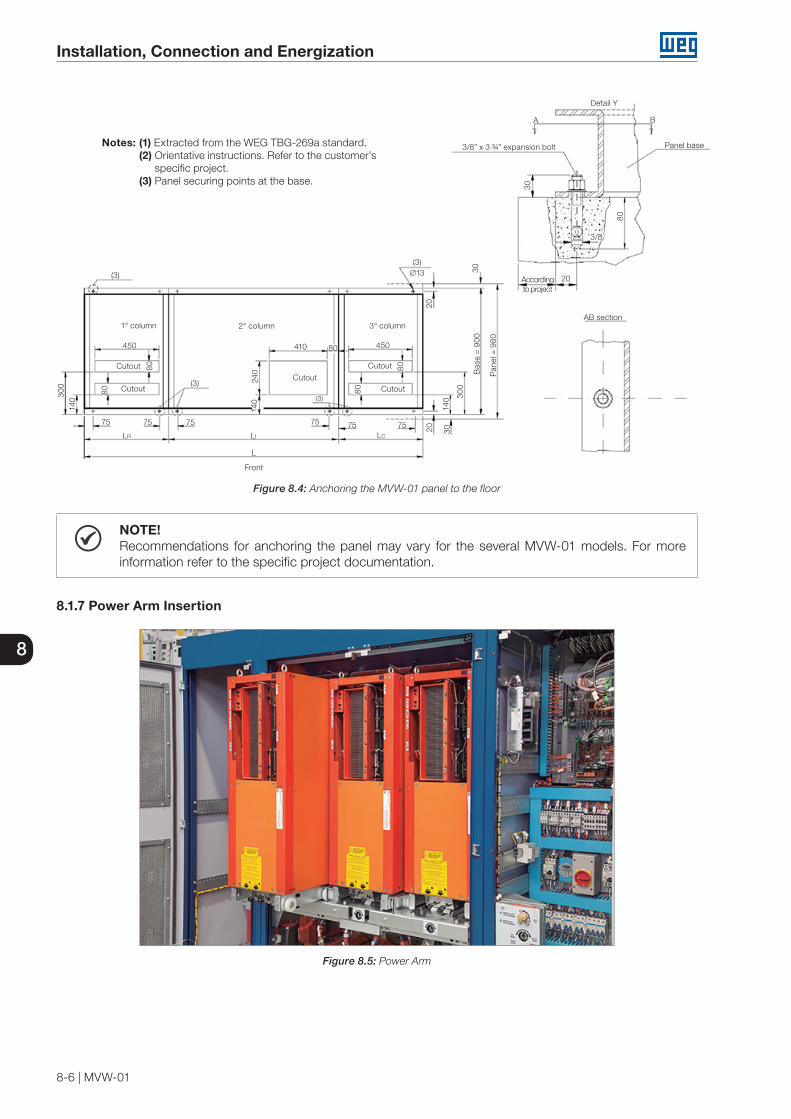
Installation, Connection and Energization
8-6 | MVW-01
8
Notes: (1) Extracted from the WEG TBG-269a standard. (2) Orientative instructions. Refer to the customer’s
specific project. (3) Panel securing points at the base.
(3)∅13
3/8” x 3 ¾” expansion bolt
30
20
Detail Y
30
A B
Panel base
80
302075
Lr
3° column2° column1° column
(3)
(3)
(3)
20
450
80
80
Cutout
Cutout
300
140
75 75 75
Li
L
Front
Cutout240
140
75 75Lc
Cutout
Cutout80
80
410 80 450
140 30
0
Bas
e =
90
0
Pan
el =
980
Accordingto project
AB section
3/8
Figure 8.4: Anchoring the MVW-01 panel to the floor
NOTE!Recommendations for anchoring the panel may vary for the several MVW-01 models. For more information refer to the specific project documentation.
8.1.7 Power Arm Insertion
Figure 8.5: Power Arm

Installation, Connection and Energization
MVW-01 | 8-7
8
Figure 8.6: Power arm insertion/extraction/movement trolley
The power arm insertion must be performed with the help of the transport trolley (WEG part number 11136572), as shown in Figure 8.6 on page 8-7 and according to the following procedure.
NOTE!During the power arm transport, they must have the locking mechanism active and be transported close to the floor (Figure 8.7 on page 8-8 - picture 1).
1. Rotate the crank handle until the trolley reaches the floor level.2. Push the arm onto the trolley rails and activate the locking mechanism.3. Move the transport trolley close to the panel, lifting the power arm to the required height and insert the trolley
tabs at the position shown in Figure 8.7 on page 8-8 - pictures 1, 2 and 3.4. Lock the trolley wheels.5. Release the lock that secures the arm to the trolley (Figure 8.7 on page 8-8 - picture 4) and push it observing
the alignment of the wheels with the base in the panel. 6. The arm must be manually inserted until the locking system (locking pin) is activated (Figure 8.7 on page 8-8
- picture 5).7. The final insertion stage is done using a crank handle, continuing the insertion to the point the second locking
pin engages (Figure 8.7 on page 8-8 - pictures 5 and 6).

Installation, Connection and Energization
8-8 | MVW-01
8
1 2
3 4
5 6
Figure 8.7: Details of the arm insertion stages
8.1.8 Power Arm Electric and Fiber Optic Connections
After inserting the power arms (U, V and W phases) connect the fiber optic cables and the supply cables according to the labels presented on the arms and on the cables.
The identifications of the cables are presented in the Table 8.2 on page 8-8 and Table 8.3 on page 8-9.
Table 8.2: Fiber optic cables identification
Identification on theFiber Optic Cable
Identificationon the Arm
1 GS1x-N1-FOI x GS12 GS2x-N2-FOI x GS23 GS3x-N3-FOI x GS34 GS4x-N4-FOI x GS45 VST1x-N5-FOI x VST16 VST2x-N6-FOI x VST27 VST3x-N7-FOI x VST38 VST4x-N8-FOI x VST49 TEMPx-N9-FOI x TEMP10 OSAx-N10-FOI x OSA11 OSBx-N11-FOI x OSB

Installation, Connection and Energization
MVW-01 | 8-9
8
Table 8.3: Power arms supply cables identification
Identification on theArm Supply Cable
Identificationon the Arm
1 BIX XC1
Note: The fiber optic cables must be handled with caution, in order not to fold, bend, squeeze or cut them.Hold the cables only at their connectors when inserting or removing them, and never apply pressure or tensile force on the fiber.
Figure 8.8: Details of the power arm supply and fiber optic cables installation stages
NOTE!In order to extract the power arms follow the procedures described in the previous sections in reverseorder.
8.1.9 Insertion of the MVW-01C Power Arms
Figure 8.9: Power arms inserted in the MVW-01C

Installation, Connection and Energization
8-10 | MVW-01
8
The power arm insertion must be performed with the help of the transport trolley (WEG part number 11136572), and according to the following procedure.
NOTE!During the power arm transport, they must have the locking mechanism engaged.
Table 8.4: Description of the power arm insertion procedure
Picture Insertion Procedure
1
1. Place the power arm on the transport trolley observing the proper locking with the locking pin.
2. Lift the arm to the necessary height and bring the trolley close to the panel.
2
3. Align the trolley guides with the inverter base according to the picture 2.
4. Pay attention to the ISOX board supply cable, which cannot be on the insertion base in the panel at the moment of the arm insertion.
5. Lock the trolley wheels.
36. Release the lock that secures the arm to the trolley according to
the picture 3.

Installation, Connection and Energization
MVW-01 | 8-11
8
Picture Insertion Procedure
47. Holding on both power arm handles, push it observing the alignment
of the wheels with the base in the panel.
58. The arms must be inserted to the point that the locking pin engages.
Observe the label about the insertion end, as shown in picture 5.
6 9. The power arm insertion procedure is complete.
NOTE!In order to extract the power arms follow the procedures described in the previous sections in reverse order.

Installation, Connection and Energization
8-12 | MVW-01
8
Table 8.5: Procedure for the installation of power supply and fiber optic cables on the power arms
Picture Connection Procedure
1
1. Connect the gate (GS1, GS2, GS3 and GS4) and status (VST1, VST2, VST3 and VST4) fiber optic cables according to the picture 1.
Note: The fiber optic cables must be handled with caution, in order not to crumple, bend, crush or cut them. Apply force only on the connectors and never on the cable while inserting or removing the fiber optic cables.
2
2. In order to connect the ISOX fiber optic cables and the power supply cable, it is necessary to remove the protective acrylic cover.
3. Connect the optic fibers OSA, OSB, and TEMP, and the power supply cable XC1, according to the picture 2.
34. Reinstall the protective acrylic cover.5. The installation of the power supply cable and fiber optic cables is
complete.
8.2 ELECTRICAL INSTALLATION
8.2.1 Power Section
The power cables that connect the supply line to the main circuit breaker and the circuit breaker to the input transformer primary must be sized for the specified voltage and current. Refer to the cubicle (main circuit breaker) and transformer documentation, strictly following all the recommendations.
The power cables that connect the input, transformer secondary windings to the MVW-01 rectifier column and
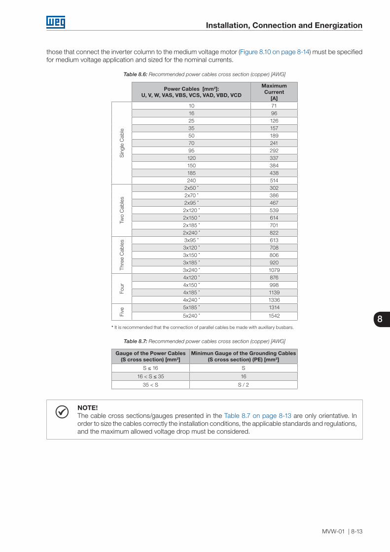
Installation, Connection and Energization
MVW-01 | 8-13
8
those that connect the inverter column to the medium voltage motor (Figure 8.10 on page 8-14) must be specified for medium voltage application and sized for the nominal currents.
Table 8.6: Recommended power cables cross section (copper) [AWG]
Power Cables [mm2]:U, V, W, VAS, VBS, VCS, VAD, VBD, VCD
Maximum Current
[A]
Sin
gle
Cab
le
10 7116 9625 12635 15750 18970 24195 292120 337150 384185 438240 514
Two
Cab
les
2x50 * 3022x70 * 3862x95 * 4672x120 * 5392x150 * 6142x185 * 7012x240 * 822
Thre
e C
able
s 3x95 * 6133x120 * 7083x150 * 8063x185 * 9203x240 * 1079
Four
4x120 * 8764x150 * 9984x185 * 11394x240 * 1336
Five
5x185 * 1314
5x240 * 1542
* It is recommended that the connection of parallel cables be made with auxiliary busbars.
Table 8.7: Recommended power cables cross section (copper) [AWG]
Gauge of the Power Cables(S cross section) [mm2]
Minimun Gauge of the Grounding Cables(S cross section) (PE) [mm2]
S ≤ 16 S
16 < S ≤ 35 16
35 < S S / 2
NOTE!The cable cross sections/gauges presented in the Table 8.7 on page 8-13 are only orientative. In order to size the cables correctly the installation conditions, the applicable standards and regulations, and the maximum allowed voltage drop must be considered.

Installation, Connection and Energization
8-14 | MVW-01
8
Transformer
(*)
(*)
MVW-01
PE U V W PEPE W V U
PEPE
Shield
PrimaryVAS VBS VCS
VAD VBD VCD
(*) If shielded cables are used between thetransformer and the inverter, then connectthe shield to the protective earth (PE) at bothextremes of the cables.
Figure 8.10: Power and ground connections
Minimum cable insulation voltage:
Table 8.8: Minimum insulation voltage of the power cables
Rated Voltage [kV] Minimum Insulation Voltage [kV]2.3 3.6/6
3.3 and 4.16 6/106.9 8.7/15
Commercial examples:
Belden: 37540.
Cofiban: Cofialt 7 kV (without shield).
Pirelli: Eprotenax 6/10 kV.
Ficap: Fibep or EPDry 6/10 kV.
Use proper terminations for the power connections as well as for the shield connections to the ground bar.
Tighten the connections with the appropriate torque.
Table 8.9: Power connections cable lugs and tightening torque
Identification Column Cable Lug Torque [Nm]±20 %
VAD
Rectifier M10 30
VBDVCDVASVBSVCS
U
Inverter M12 60VWPE
Shields Rectifier and Inverter M8 15

Installation, Connection and Energization
MVW-01 | 8-15
8
DANGER! It is mandatory to connect the inverter to a protection ground (PE). The grounding connection must
follow the local regulations. Use at least conductors with the wire gauge indicated in the Table 8.7 on page 8-13. Connect the inverter to a specific grounding rod or to the general ground system (resistance ≤ 10 Ohms), the transformer frame ground for instance.
Never connect the input transformer secondary windings to the ground.
DANGER! Il est obligatoire de connecter l’onduleur à un connecteur de mise à la terre (PE). La connexion
de mise à la terre doit suivre les règlementations locales. Utilisez au moins des conducteurs avec le calibre de fil indiqué dans le Table 8.7 on page 8-13. Connectez l’onduleur à une tige de mise à la terre spécifique ou au système de mise à la terre général (résistance ≤ 10 ohms), la terre du cadre du transformateur par exemple.
Ne connectez jamais les enroulements secondaires du transformateur d’entrée à la terre.
8.2.2 Input Circuit Breaker
The MVW-01 operates the input circuit breaker. This circuit breaker must have minimum voltage, closing and opening coils. The power supply for the circuit breaker circuits comes from the MVW-01. The following signals, provided by the circuit breaker, are necessary for its operation: Ready, On, Off and Trip. These signals must be dry contacts (potential free).
The MVW-01 also has inputs for the indications of input transformer alarm and fault.
Ready
Line
Circuit breaker
Protection
SO
No fault
ON OFF
Commandpower supply
Minimumvoltage
coil(U<)
220 Vac
(2)
ON OFF
MVW-015 6 7 8321x12:
220 VdcInverterready
Off
link > 50 %
On
Commands220 Vac
Emergency
DI4
DI3
DI5
DI2
5 4321x10:+24 VPS24
OFFON
FaultCB tripReady
Feedback
Notes:(1) 24 Vdc wiring: use shielded cables and keep them distant from power and command wiring.(2) 220 Vac wiring: keep it distant from the power wiring.
Rectifier+
Inverter
INPUT CIRCUIT BREAKER CUBICLE
(1)
M3~(1)
4
Figure 8.11: Connections between the input circuit breaker and the inverter
ATTENTION!The input circuit breaker must only be closed by the inverter, otherwise the transformer and the inverter may be damaged.

Installation, Connection and Energization
8-16 | MVW-01
8
DANGER!Although the inverter commands the opening of the circuit breaker, there is no guarantee of its opening. In order to open the medium voltage cabinets for maintenance, follow all the procedures of safe de-energization (refer to the Item 8.3.4 Safe De-energization Instructions on page 8-19).
DANGER!Bien que l’onduleur commande l’ouverture du coupe-circuit, il n’y a pas de garantie qu’il s’ouvre. Afin d’ouvrir les armoires moyenne tension pour la maintenance, suivez toutes les procédures de mise hors tension (élément Item 8.3.4 Safe De-energization Instructions on page 8-19).
NOTE!It is recommended that the MVW-01 Kirk key is interlocked with the ring welded to the key of the input cubicle.
MVW-01C ELECTRICAL INSTALLATION
VADE1 VBDE1 VCDE1
VAD VBD VCD
VADE2 VBDE2 VCDE2
PE U V W PE
MVW-01C
PE W V U
Blindagem PE
Primário
PE
* Caso se utilize cabos blindados entre o transformador e o inversor, conectar a blindagem ao terra de proteção (PE) em ambas as extremidades.
Transformador
Transformer
* If shielded cables are used between the transformer and the inverter, then connect the shield to the protective earth (PE) at both extremes of the cables.
Shield
MVW-01C
Primary
VADE1VBDE1 VCDE1
VADE2VBDE2 VCDE2
VADVBD VCD
PE PE
PE U V W PE
PE W V U
Figure 8.12: Power and ground connections
Table 8.10: Power connections cable lugs and tightening torque
Identification Column Cable Lug Torque [Nm]± 20 %
VADE1, VBDE1 and VCDE1 Rectifier M1030VAD, VBD and VCD Rectifier M10
VADE2, VBDE2 and VCDE2 Rectifier M10U Rectifier
M1260
V RectifierW RectifierPE Rectifier M12
Shields Rectifier M8 15
8.2.3 Low Voltage Auxiliary Supply
Control column power supply nominal voltage selectionAn auxiliary voltage supply (220 V-480 V) should be available in the installation. This voltage must be wired to the terminal strip present in the control column. The command transformer (T1) taps must be selected according to the available auxiliary voltage. For more details, refer to the MVW-01 electrical project.
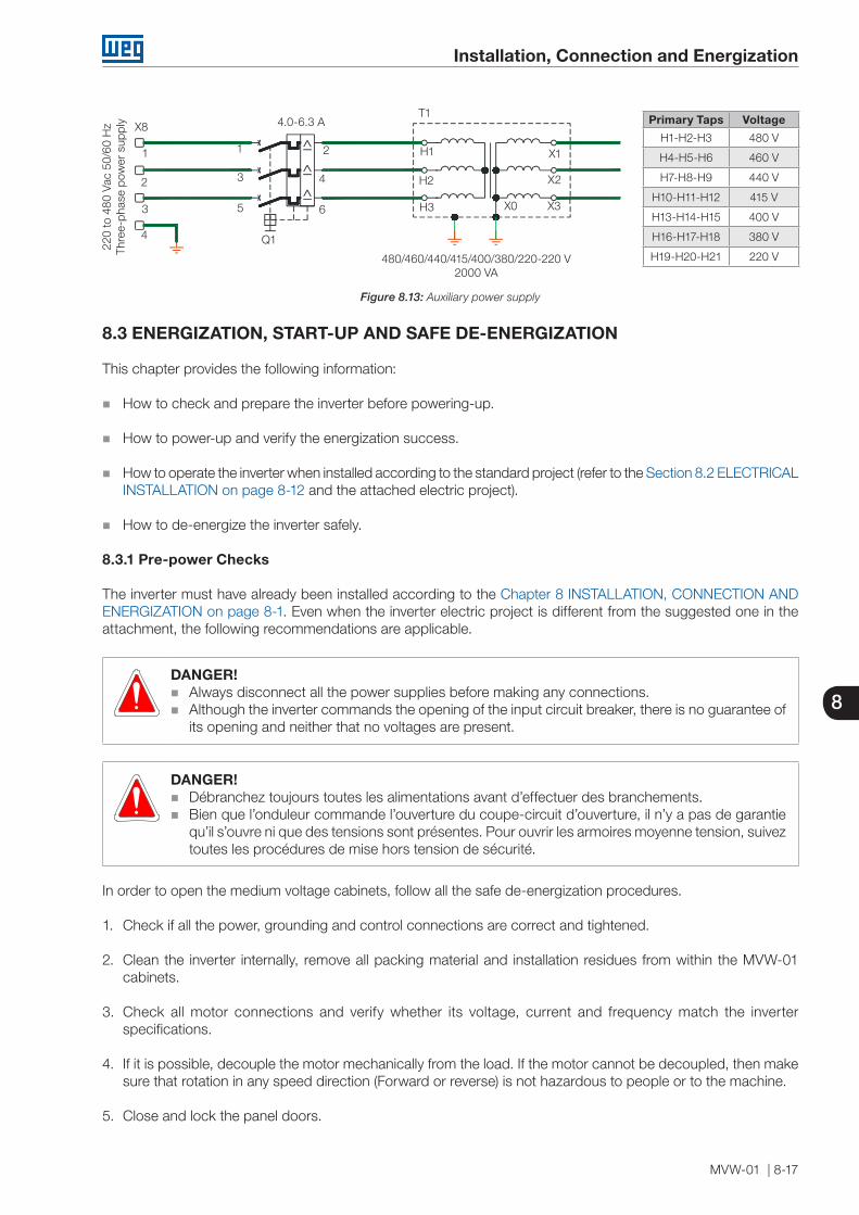
Installation, Connection and Energization
MVW-01 | 8-17
8
Primary Taps Voltage
H1-H2-H3 480 V
H4-H5-H6 460 V
H7-H8-H9 440 V
H10-H11-H12 415 V
H13-H14-H15 400 V
H16-H17-H18 380 V
H19-H20-H21 220 V
1
220
to 4
80 V
ac 5
0/60
Hz
Thre
e-ph
ase
pow
er s
uppl
y X8
2
3
4
1
3
5
Q1
4.0-6.3 A
2
4
T1
H1
H2
H3
X1
X2
X3X0
480/460/440/415/400/380/220-220 V2000 VA
6
Figure 8.13: Auxiliary power supply
8.3 ENERGIZATION, START-UP AND SAFE DE-ENERGIZATION
This chapter provides the following information:
How to check and prepare the inverter before powering-up.
How to power-up and verify the energization success.
How to operate the inverter when installed according to the standard project (refer to the Section 8.2 ELECTRICAL INSTALLATION on page 8-12 and the attached electric project).
How to de-energize the inverter safely.
8.3.1 Pre-power Checks
The inverter must have already been installed according to the Chapter 8 INSTALLATION, CONNECTION AND ENERGIZATION on page 8-1. Even when the inverter electric project is different from the suggested one in the attachment, the following recommendations are applicable.
DANGER! Always disconnect all the power supplies before making any connections. Although the inverter commands the opening of the input circuit breaker, there is no guarantee of
its opening and neither that no voltages are present.
DANGER! Débranchez toujours toutes les alimentations avant d’effectuer des branchements. Bien que l’onduleur commande l’ouverture du coupe-circuit d’ouverture, il n’y a pas de garantie
qu’il s’ouvre ni que des tensions sont présentes. Pour ouvrir les armoires moyenne tension, suivez toutes les procédures de mise hors tension de sécurité.
In order to open the medium voltage cabinets, follow all the safe de-energization procedures.
1. Check if all the power, grounding and control connections are correct and tightened.
2. Clean the inverter internally, remove all packing material and installation residues from within the MVW-01 cabinets.
3. Check all motor connections and verify whether its voltage, current and frequency match the inverter specifications.
4. If it is possible, decouple the motor mechanically from the load. If the motor cannot be decoupled, then make sure that rotation in any speed direction (Forward or reverse) is not hazardous to people or to the machine.
5. Close and lock the panel doors.

Installation, Connection and Energization
8-18 | MVW-01
8
8.3.2 Initial Power-up (Parameter Settings)
After the pre-power checks the inverter can be powered up:
1. Verify the supply voltages Verify whether the medium voltage line is available at the input cubicle. Measure the auxiliary low voltage power supply voltage that feeds the control column and make sure it is within
the allowed limits of +10 % / -15 %.
2. Check the control column circuit breakers Verify if the settings of the control circuit breakers are according to the electric project. Close the control column
door.
3. Verify the emergency pushbutton Make sure the emergency pushbutton is not actuated. In case it is actuated, use the safety key to unlock it.
4. Apply power to the control column Close the control column auxiliary supply disconnector switch only after the power-up process be concluded.
5. Verify the first energization success The first time the panel is energized or when the factory settings are loaded with P204 = 5, the guided start-
up routine is initiated. This routine asks the user to program some parameters regarding the inverter and the motor.
8.3.3 Start-up
This section describes the inverter start-up with keypad operation. The considered control mode is V/F 60 Hz.
DANGER! High voltages may be present even after the power supply disconnection. The following sequence is valid for the standard MVW-01 inverter. The inverter should have already
been installed and programmed, according to Chapter 8 INSTALLATION, CONNECTION AND ENERGIZATION on page 8-1.
DANGER! Des tensions élevées peuvent être présentes même après déconnexions de l’alimentation. La séquence suivante est valable pour l’onduleur du MVW-01 standard. L’onduleur doit déjà
avoir été installé et programmé, comme décrit respectivement dans le Chapter 8 INSTALLATION, CONNECTION AND ENERGIZATION on page 8-1.
8.3.3.1 Start-up with HMI Operation and V/F 60 Hz Control Mode
1. Apply power to the panel close the disconnector switch at the control column power supply input.
2. Once the control column has been energized, the MVC1 or MVC3 control board waits for its initialization, presenting the following message on the HMI:
- After the control has finished its initialization (approximately 10 seconds), the message “Inverter in Undervoltage” is presented on the HMI.
At this moment the inverter is in undervoltage state (DC link is discharged) and the “Ready to Start” pilot light (H1)at the control column door is on, indicating that it is already possible to initiate the inverter pre-charge.
3. Initiate the pre-charge / power section energization.The MVW-01 inverter pre-charge command must be given manually:
With the pilot light “READY TO START” on, press the “POWER-ON” pushbutton (S1).
Installation, Connection and Energization
MVW-01 | 8-19
8
Wait until the pre-charge is finished (approximately 10 seconds). During the pre-charge the “PRECHARGE” pilot light (H2) must remain on.
Once the pre-charge is successfully completed, the “PRE-CHARGE” pilot light goes off and the “INPUT ON” (H3) goes on, indicating that the input transformer circuit breaker was successfully closed.
The “Inverter Ready” message is displayed on the HMI.
NOTE!The maximum number of pre-charge procedures that can be performed per hour must be established by the auxiliary transformer supplier.
ATTENTION!If during the pre-charge any problem occurs, the inverter indicates an error related to it. The possible errors are:F014 - Fault in the input transformer circuit breaker closure.F017 - Circuit breaker not ready.F020 - Pre-charge fault.Refer to these error (alarm/fault) descriptions in the Section 14.1 ALARMS/FAULTS AND POSSIBLE CAUSES on page 14-1.
NOTE!
The last speed reference value, set via the and keys, is saved in the memory.If you want to change this value before enabling the inverter, change it through the parameter P121(Keypad Speed Reference), which stores the keypad speed reference.
NOTES:1. If the motor speed direction is inverted, switch off the inverter following the safe de-energization instructions
and swap two of the motor cables. The HMI must indicate the same direction seen looking against the motor shaft end.
2. It the current is too high during the acceleration, especially at low speeds, it is necessary to reduce the acceleration ramp time (P100 or P102) or change P136 - Torque boost setting.
Gradually increase and decrease the P136 content until reaching an operation with approximately constant current throughout the entire speed range. Refer to the parameter description in Chapter 11 DETAILED PARAMETER DESCRIPTION on page 11-1.
3. If F022 occurs during the deceleration, then increase its time via P101 or P103 and check P151.
ATTENTION!If the inverter receives a general enabling or a start command before the pre-charge has been finished (inverter still in undervoltage state), the command will be ignored and a warning message “Inverter Undervoltage” will be displayed on the HMI.
8.3.4 Safe De-energization Instructions
DANGER! Although the inverter commands the opening of the input circuit breaker, there is no guarantee of
its opening and neither that no voltages are present, because the capacitors remain charged for a long time and they can also be charged through the auxiliary supply (pre-charge).
In order to open the medium voltage cabinets, follow all the safe de-energization procedures described next.
Installation, Connection and Energization
8-20 | MVW-01
8
DANGER! Bien que l’onduleur commande l’ouverture du coupe-circuit d’entrée, il n’y a aucune garantie qu’il
s’ouvrira ni qu’aucune tension n’est présente, car les condensateurs restent chargés pendant longtemps et ils peuvent également être chargés par l’alimentation auxiliaire (précharge).
Pour ouvrir les armoires moyenne tension moyenne, suivez toutes les procédures de mise hors tension de sécurité décrites ci-dessous.
1. Decelerate the motor to a complete stop.
2. Check the DC link voltage at the parameter P004 on the HMI. Open the control panel door and locate the neon lamps of the HVM (High Voltage Monitoring board), mounted on the cabinet left side. The four lamps must be on if the voltage showed via P004 is above 200 V.
3. Press the “POWER OFF” pushbutton. The input transformer circuit breaker is switched off at this moment, and the “INPUT ON” pilot light going off indicates it.
ATTENTION!If the input transformer circuit breaker does not open with the “POWER OFF” command, then open it manually.
4. Follow the DC link voltage decrease through P004 on the HMI and the HVM neon lamps. When the DC link voltage crosses below 200 V the neon lamps start flashing with progressively lower frequency until going off completely.
Wait until the DC link voltage displayed at P004 on the HMI gets below 25 V.
5. At the input transformer circuit breaker cubicle, extract the circuit breaker from its operation position and close the transformer primary winding grounding switch. Lock the cubicle with the key and/or put a warning sign “System in maintenance”.
6. Press the emergency pushbutton located on the control column door and remove its key.
7. Switch off the Q2 circuit breaker in the control column and lock it in the open position with a padlock and/or put a warning sign “System in maintenance”.
8. Switch off the Q1 circuit breaker in the control column. Remove the auxiliary power supply.
It is only after the sequence of procedures described here that medium voltage compartment doors can be opened.
DANGER!If it were not possible to follow the discharge of the DC link capacitors through the parameter P004,as well as through the HVM board neon lamps, due to a malfunction or a previous de energization,follow the instructions 5) through 8) and wait 10 minutes more.
DANGER!S’il n’était pas possible de suivre la décharge des condensateurs de liaison CC avec le paramètre P004 et les lampes à néon de la carte HVM en raison d’un dysfonctionnement ou une mise hors tension préalable, suivez les instructions 5) jusqu’à 8) et attendez 10 minutes supplémentaires.

Keypad (HMI) Operation
MVW-01 | 9-1
9
9 KEYPAD (HMI) OPERATION
The Graphic HMI Interface (HMI - Human Machine Interface) provides a series of new resources to the mediumvoltage frequency inverter MVW-01. They are:
Visualization: text and graphic visualization modes.
Monitoring: up to 6 parameters can be monitored simultaneously on the screen.
Navigation: navigation system via menus, with the addition of scroll bars and new keys.
On-line help function: help in the own HMI (in 3.0x and latest versions, help for parameters an errors).
Editing: new keys to speed up the parameter edition.
The graphic HMI design, improvements and new functions present an operation, navigation and programming similar to the HMI used with the CFW-11 line, making its use even easier to those familiar with that WEG product line (refer to the Figure 9.1 on page 9-1).
Inverter status Motor speed
Speed direction Local/Remote
Time
Softkey 1 function Softkey 2 function
Softkey 1 Softkey 2
Prog/Enter key
Help key
Available help
Figure 9.1: MVW-01 inverter Graphic HMI
NOTE!The MVW-01 3.xx version requires the use of an updated version of the Graphic HMI called Graphic HMI 2 or HMIG2. Therefore, it is not possible to use the conventional Graphic HMI with a 3.xx firmware set.
NOTE!The HMIG2 upgrades are summarized in the increase of the RAM and ROM memory capacities, so that the operation is identical for both cases and, therefore, no distinctions will be made between the HMIG2 and the former Graphic HMI in the descriptions of this manual.

Keypad (HMI) Operation
9-2 | MVW-01
9
9.1 INSTALLATION OF THE GRAPHIC HMI IN THE CABINET
The installation of the HMI in the cabinet is done without the need of using the frame, and the fastening is done directly through the screws placed on the movable fins positioned at the HMI back cover, according to the Figure 9.2 on page 9-2.
R4
16Fastener
187107
Figure 9.2: Size of the panel cut-out for fixing the Graphic HMI
The connection of the Graphic HMI to the MVC4 board is done with the same cable used for the conventionalHMI, and the connection point on the MVC4 board is also the XC8 connector.
NOTE! No additional hardware configuration has to be done on the MVC4 board, because it recognizes
the type of connected HMI automatically. The MVC4 board and the Graphic HMI software versions must be compatible. For instance, if
the Graphic HMI software is 3.0X and the MVC4 board version is 3.1X or newer, the HMI will not work properly and a warning of incompatible software version will occur.
ATTENTION!It is not recommended to connect the Graphic HMI to the MVC4 board with power applied to the control rack.
9.2 STARTING THE USE OF THE GRAPHIC HMI
The communication between the Graphic HMI and the inverter is established with the Modbus RTU protocol (38400 bps, no parity, with 2 stop bits), using as the physical layer the channel. The Graphic HMI works as the communication master.When the panel is energized the Graphic HMI performs a parameter initialization with the MVC4 board. During this process the firmware versions of the Graphic HMI and of the MVW-01 control boards are exhibited.
The information of the parameters being transferred and a progress bar are also exhibited during the initializationprocess (refer to the Figure 9.3 on page 9-3).

Keypad (HMI) Operation
MVW-01 | 9-3
9
SW Version HMI2 3.2XSW Version MVC4 3.2XSW Version MVC3 3.2X
Figure 9.3: Graphic HMI initialization
NOTE! In order to be able to start using the Graphic HMI (navigation and parameter edition) it is only
necessary that the initialization be successfully concluded and no additional programming is necessary.
The values of the parameters remain stored in the MVC4 board. If a communication problem occurs and the initialization is not successfully concluded, the Graphic HMI notifies an initialization failure and releases the keypad use, however, any modification in the parameter programming becomes useless because data will not be sent to the MVC4 board.
If the Graphic HMI is disconnected while the panel is with power, when reconnecting it a new initialization procedure occurs.
9.2.1 Graphic HMI Basic Visualization Modes
In any HMI use situation (visualization mode or active screen) there are standard indications that always will be presented (refer to the Figure 9.1 on page 9-1):
Header:
Inverter Status.
Speed Direction.
Help Availability.
Local or Remote Mode.
Motor Speed (rpm).
Footer:
Time.
Function of the 2 Softkeys.
The various modules or visualization screens of the Graphic HMI can be classified into 6 distinct basic types: Read-only parameters:
1 parameter.
2 to 4 parameters.
5 or 6 parameters.
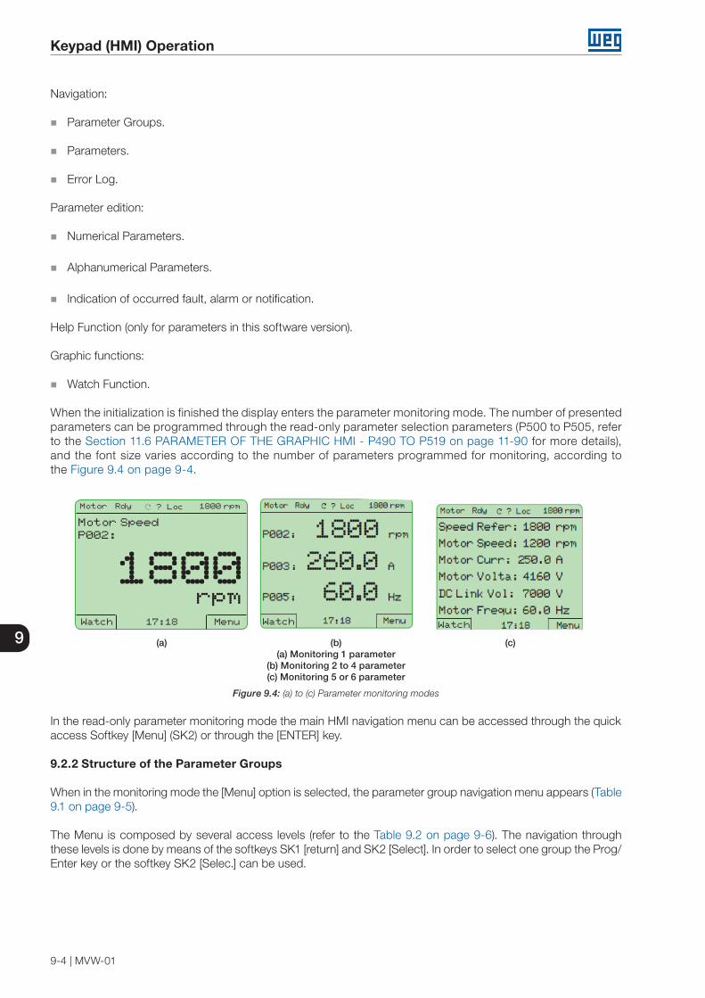
Keypad (HMI) Operation
9-4 | MVW-01
9
Navigation:
Parameter Groups.
Parameters.
Error Log.
Parameter edition:
Numerical Parameters.
Alphanumerical Parameters.
Indication of occurred fault, alarm or notification.
Help Function (only for parameters in this software version).
Graphic functions:
Watch Function.
When the initialization is finished the display enters the parameter monitoring mode. The number of presented parameters can be programmed through the read-only parameter selection parameters (P500 to P505, refer to the Section 11.6 PARAMETER OF THE GRAPHIC HMI - P490 TO P519 on page 11-90 for more details), and the font size varies according to the number of parameters programmed for monitoring, according to the Figure 9.4 on page 9-4.
Motor Rdy ? Loc 1800 rpm
17:18 MenuWatch
Motor SpeedP002:
rpm1800
Watch Watch
(a) (b) (c)(a) Monitoring 1 parameter
(b) Monitoring 2 to 4 parameter(c) Monitoring 5 or 6 parameter
Figure 9.4: (a) to (c) Parameter monitoring modes
In the read-only parameter monitoring mode the main HMI navigation menu can be accessed through the quickaccess Softkey [Menu] (SK2) or through the [ENTER] key.
9.2.2 Structure of the Parameter Groups
When in the monitoring mode the [Menu] option is selected, the parameter group navigation menu appears (Table 9.1 on page 9-5).
The Menu is composed by several access levels (refer to the Table 9.2 on page 9-6). The navigation through these levels is done by means of the softkeys SK1 [return] and SK2 [Select]. In order to select one group the Prog/Enter key or the softkey SK2 [Selec.] can be used.
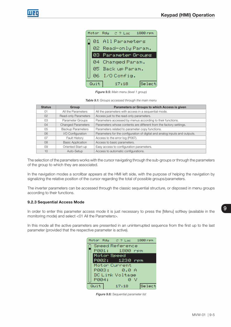
Keypad (HMI) Operation
MVW-01 | 9-5
9
Figure 9.5: Main menu (level 1 group)
Table 9.1: Groups accessed through the main menu
Status Group Parameters or Groups to which Access is given01 All the Parameters All the parameters with access in a sequential mode.02 Read-only Parameters Access just to the read-only parameters.03 Parameter Groups Parameters accessed by menus according to their functions.04 Changed Parameters Parameters whose contents are different from the factory settings.05 Backup Parameters Parameters related to parameter copy functions.06 I/O Configuration Parameters for the configuration of digital and analog inputs and outputs.07 Fault History Access to the error log (P067).08 Basic Application Access to basic parameters.09 Oriented Start-up Easy access to configuration parameters.10 Auto-Setup Access to automatic configurations.
The selection of the parameters works with the cursor navigating through the sub-groups or through the parametersof the group to which they are associated.
In the navigation modes a scrollbar appears at the HMI left side, with the purpose of helping the navigation by signalizing the relative position of the cursor regarding the total of possible groups/parameters.
The inverter parameters can be accessed through the classic sequential structure, or disposed in menu groups according to their functions.
9.2.3 Sequential Access Mode
In order to enter this parameter access mode it is just necessary to press the [Menu] softkey (available in the monitoring mode) and select <01 All the Parameters>.
In this mode all the active parameters are presented in an uninterrupted sequence from the first up to the last parameter (provided that the respective parameter is active).
Figure 9.6: Sequential parameter list
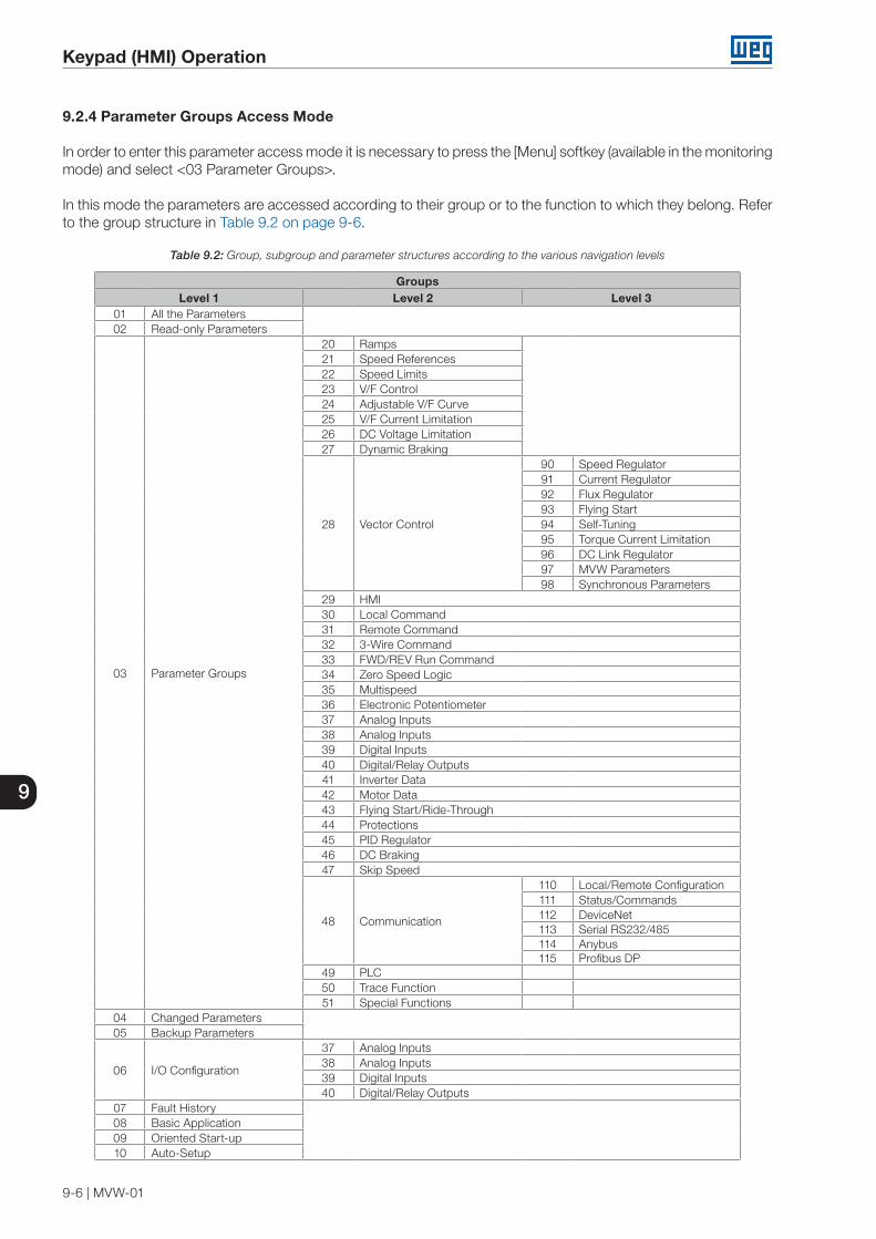
Keypad (HMI) Operation
9-6 | MVW-01
9
9.2.4 Parameter Groups Access Mode
In order to enter this parameter access mode it is necessary to press the [Menu] softkey (available in the monitoring mode) and select <03 Parameter Groups>.
In this mode the parameters are accessed according to their group or to the function to which they belong. Refer to the group structure in Table 9.2 on page 9-6.
Table 9.2: Group, subgroup and parameter structures according to the various navigation levels
GroupsLevel 1 Level 2 Level 3
01 All the Parameters02 Read-only Parameters
03 Parameter Groups
20 Ramps21 Speed References22 Speed Limits23 V/F Control24 Adjustable V/F Curve25 V/F Current Limitation26 DC Voltage Limitation27 Dynamic Braking
28 Vector Control
90 Speed Regulator91 Current Regulator92 Flux Regulator93 Flying Start94 Self-Tuning95 Torque Current Limitation96 DC Link Regulator97 MVW Parameters98 Synchronous Parameters
29 HMI30 Local Command31 Remote Command32 3-Wire Command33 FWD/REV Run Command34 Zero Speed Logic35 Multispeed36 Electronic Potentiometer37 Analog Inputs38 Analog Inputs39 Digital Inputs40 Digital/Relay Outputs41 Inverter Data42 Motor Data43 Flying Start/Ride-Through44 Protections45 PID Regulator46 DC Braking47 Skip Speed
48 Communication
110 Local/Remote Configuration111 Status/Commands112 DeviceNet113 Serial RS232/485114 Anybus115 Profibus DP
49 PLC50 Trace Function51 Special Functions
04 Changed Parameters05 Backup Parameters
06 I/O Configuration
37 Analog Inputs38 Analog Inputs39 Digital Inputs40 Digital/Relay Outputs
07 Fault History08 Basic Application09 Oriented Start-up10 Auto-Setup

Keypad (HMI) Operation
MVW-01 | 9-7
9
Figure 9.7: Navigation through the group 03 (Parameter Groups)
9.3 PARAMETER EDITION
The activation of the edition or parameter changing mode is executed by pressing the Enter/Prog key or the softkeyassociated to the parameter navigation.
Once in the edition mode, if the softkey programmed to leave [Return] is used, the modifications are not stored in the parameter memory and the value prior to the edition is restored. In a similar way, by using the softkey programmed to confirm [Select], the new parameter content is stored in the inverter parameter memory.
9.3.1 Numerical
The numerical parameters (refer to the Figure 9.8 on page 9-7) are changed with the and keys, in order to increment and decrement their contents. There is the possibility of changing the parameter contents with a ten times faster rate (x 10), therefore, the and keys are used in order to increment and decrement the tens.
Figure 9.8: Numerical edition
9.3.2 Alphanumerical
In the edition of message type parameters (refer to the Figure 9.9 on page 9-7) the cursor can be moved with the and .
Figure 9.9: Alphanumerical edition
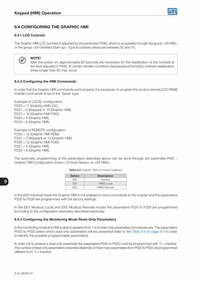
Keypad (HMI) Operation
9-8 | MVW-01
9
9.4 CONFIGURING THE GRAPHIC HMI
9.4.1 LCD Contrast
The Graphic HMI LCD contrast is adjusted by the parameter P490, which is accessible through the group <29 HMI> or the group <09 Oriented Start-up>. Typical contrast values are between 50 and 75.
NOTE!After the power on, approximately 60 seconds are necessary for the stabilization of the contrast at the level adjusted in P490. In certain climatic conditions (temperature/humidity) contrast stabilization times longer than 60 may occur.
9.4.2 Configuring the HMI Commands
In order that the Graphic HMI commands work properly, it is necessary to program the local or remote (LOC/REM)inverter commands to be of the ‘Serial’ type.
Example of LOCAL configuration:P220 = 11 (Graphic HMI LOC).P221 = 0 (Keypad) or 13 (Graphic HMI).P223 = 12 (Graphic HMI FWD).P224 = 5 (Graphic HMI).P225 = 6 (Graphic HMI).
Example of REMOTE configuration:P220 = 12 (Graphic HMI REM).P222 = 0 ((Keypad) or 13 (Graphic HMI).P226 = 12 (Graphic HMI FDW).P227 = 5 (Graphic HMI).P228 = 6 (Graphic HMI).
The automatic programming of the parameters described above can be done through the parameter P491 - Graphic HMI Configuration (menu <10 Auto-Setup> or <29 HMI>).
Table 9.3: Graphic HMI commands selection
Option Description000 Inactive001 HMIG Local002 HMIG Remote
In the [000 Inactive] mode the Graphic HMI is not enabled to send commands to the inverter and the parametersP220 to P228 are programmed with the factory settings.
In the [001 Modbus Local] and [002 Modbus Remote] modes the parameters P220 to P228 are programmed according to the configuration examples described previously.
9.4.3 Configuring the Monitoring Mode Read-Only Parameters
In the monitoring mode the HMI is able to present from 1 to 6 read-only parameters simultaneously. The parametersP500 to P505 select which read-only parameters will be presented (refer to the Table 9.4 on page 9-9 in order to identify the possible programmable parameters).
In order not to present a read-only parameter the parameters P500 to P505 must be programmed with ‘0 = Inactive’. The number of read-only parameters presented depends on how many parameters from P500 to P505 are programmed different from ‘0 = Inactive’.
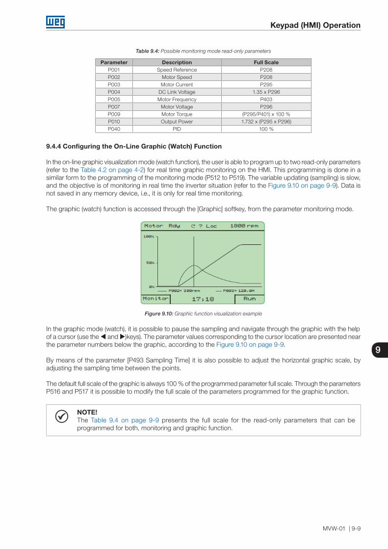
Keypad (HMI) Operation
MVW-01 | 9-9
9
Table 9.4: Possible monitoring mode read-only parameters
Parameter Description Full ScaleP001 Speed Reference P208P002 Motor Speed P208P003 Motor Current P295P004 DC Link Voltage 1.35 x P296P005 Motor Frequency P403P007 Motor Voltage P296P009 Motor Torque (P295/P401) x 100 %P010 Output Power 1.732 x (P295 x P296)P040 PID 100 %
9.4.4 Configuring the On-Line Graphic (Watch) Function
In the on-line graphic visualization mode (watch function), the user is able to program up to two read-only parameters(refer to the Table 4.2 on page 4-2) for real time graphic monitoring on the HMI. This programming is done in a similar form to the programming of the monitoring mode (P512 to P519). The variable updating (sampling) is slow, and the objective is of monitoring in real time the inverter situation (refer to the Figure 9.10 on page 9-9). Data is not saved in any memory device, i.e., it is only for real time monitoring.
The graphic (watch) function is accessed through the [Graphic] softkey, from the parameter monitoring mode.
Figure 9.10: Graphic function visualization example
In the graphic mode (watch), it is possible to pause the sampling and navigate through the graphic with the helpof a cursor (use the and )keys). The parameter values corresponding to the cursor location are presented near the parameter numbers below the graphic, according to the Figure 9.10 on page 9-9.
By means of the parameter [P493 Sampling Time] it is also possible to adjust the horizontal graphic scale, by adjusting the sampling time between the points.
The default full scale of the graphic is always 100 % of the programmed parameter full scale. Through the parametersP516 and P517 it is possible to modify the full scale of the parameters programmed for the graphic function.
NOTE!The Table 9.4 on page 9-9 presents the full scale for the read-only parameters that can be programmed for both, monitoring and graphic function.
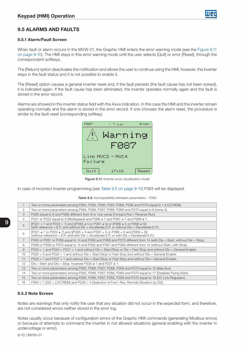
Keypad (HMI) Operation
9-10 | MVW-01
9
9.5 ALARMS AND FAULTS
9.5.1 Alarm/Fault Screen
When fault or alarm occurs in the MVW-01, the Graphic HMI enters the error warning mode (see the Figure 9.11 on page 9-10). The HMI stays in this error warning mode until the user selects [Quit] or error [Reset], through the correspondent softkeys.
The [Return] option deactivates the notification and allows the user to continue using the HMI, however, the inverterstays in the fault status and it is not possible to enable it.
The [Reset] option causes a general inverter reset and, if the fault persists (the fault cause has not been solved), it is indicated again. If the fault cause has been eliminated, the inverter operates normally again and the fault is stored in the error record.
Alarms are showed in the inverter status field with the Axxx indication. In this case the HMI and the inverter remainoperating normally and the alarm is stored in the error record. If one chooses the alarm reset, the procedure is similar to the fault reset (corresponding softkey).
17:18Quit Reset
WarningF087
Link MVC3 - MVC4Failure
F087 ? Loc 0 rpm
!
Figure 9.11: Inverter error visualization mode
In case of incorrect inverter programming (see Table 9.5 on page 9-10) F083 will be displayed.
Table 9.5: Incompatibility between parameters - F083
1 Two or more parameters among P264, P265, P266, P267, P268, P296 and P270 equal to 1 (LOC/REM).2 Two or more parameters among P265, P266, P267, P268, P269 and P270 equal to 6 (ramp 2).3 P265 equal to 8 and P266 different from 8 or vice-versa (Forward Run / Reverse Run).4 P221 or P222 equal to 8 (Multispeed) and P266 ≠ 7 and P267 ≠ 7 and P268 ≠ 7.
5 [P221 = 7 and P222 = 7] and [(P265 ≠ 5 or P267 ≠ 5) or (P266 ≠ 5 or P268 ≠ 5)](with reference = E.P. and without DIx = Accelerate E.P. or without DIx = Decelerate E.P.).
6 [P221 ≠ 7 or P222 ≠ 7] and [(P265 = 5 and P267 = 5 or P266 = 5 and P268 = 5)](without reference = E.P. and with DIx = Accelerate E.P. or with DIx = Decelerate E.P.).
7 P265 or P267 or P269 equal to 14 and P266 and P268 and P270 different from 14 (with DIx = Start, without DIx = Stop).8 P266 or P268 or P270 equal to 14 and P265 and P267 and P269 different from 14 (without Start, with Stop).9 P220 > 1 and P224 = P227 = 1 and without DIx = Start/Stop or DIx = Fast Stop and without DIx = General Enable.10 P220 = 0 and P224 = 1 and without DIx = Start/Stop or Fast Stop and without DIx = General Enable.11 P220 = 1 and P227 = 1 and without DIx = Start/Stop or Fast Stop and without DIx = General Enable.12 DIx = Start and DIx = Stop, however P224 ≠ 1 and P227 ≠ 1.13 Two or more parameters among P265, P266, P267, P268, P269 and P270 equal to 15 (Man/Aut).14 Two or more parameters among P265, P266, P267, P268, P269 and P270 equal to 17 (Disables Flying Start).15 Two or more parameters among P265, P266, P267, P268, P269 and P270 equal to 18 (DC Link Regulator).16 P264 = 1 (DI2 = LOC/REM) and P226 = 4 (Selection of Fwd / Rev, Remote Situation by DI2).
9.5.2 Note Screen
Notes are warnings that only notify the user that any situation did not occur in the expected form, and therefore,are not considered errors neither stored in the error log.
Notes usually occur because of configuration errors of the Graphic HMI commands (generating Modbus errors) or because of attempts to command the inverter in not allowed situations (general enabling with the inverter in undervoltage or error).

Keypad (HMI) Operation
MVW-01 | 9-11
9
NOTE!Notes do not generate events as inverter stopping.
Figure 9.12: Inverter note screen
9.5.3 Error Log
The parameter P067 keeps the information on the inverter last 100 occurred errors (in a similar manner to the conventional HMI), according to the Figure 9.13 on page 9-11.
In order to visualize more information regarding the error, as its description and the status of the inverter at the moment it occurred, it is necessary to select the [+Info] option through the corresponding softkey (refer to the Figure 9.13 on page 9-11).
(a) Error Log P067
(b) More information on the error
Figure 9.13: (a) and (b) - More information on the error
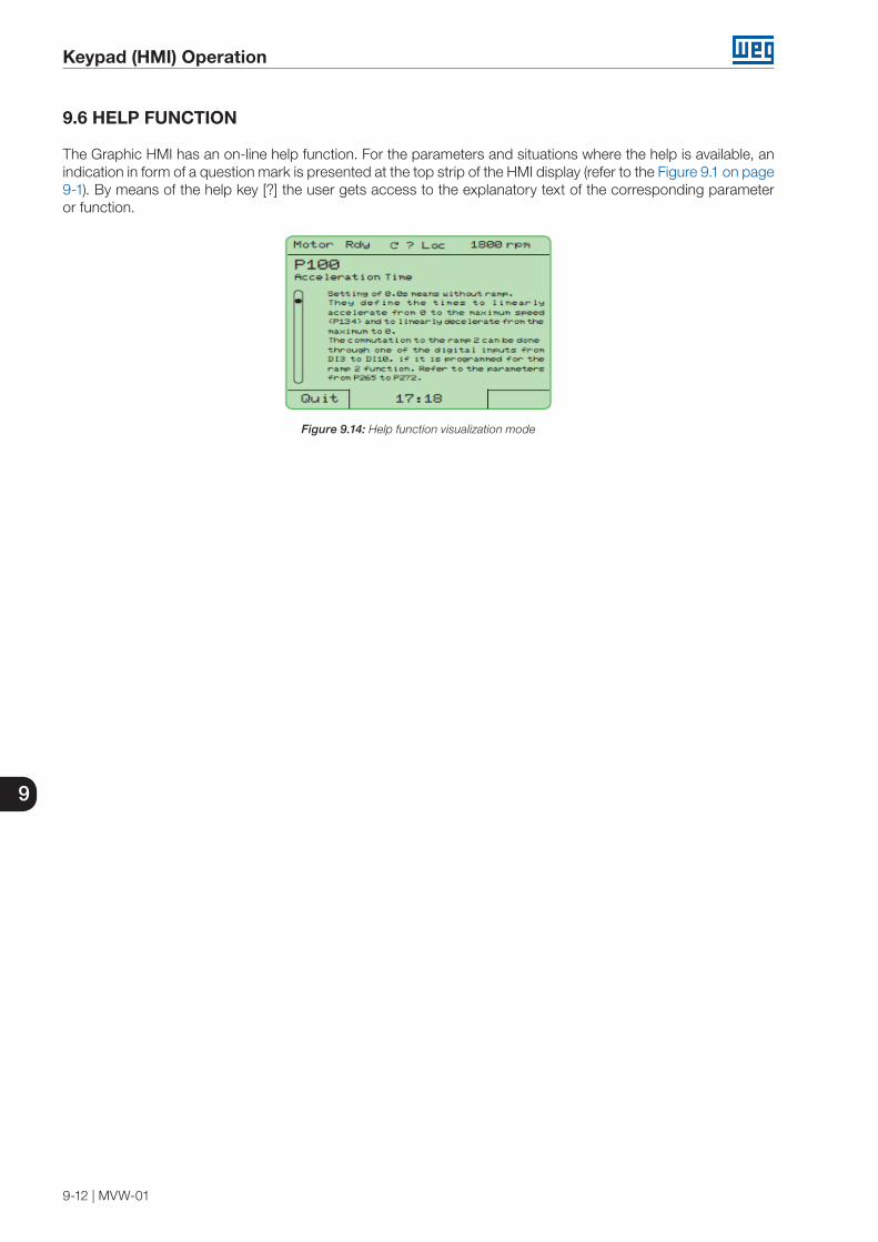
Keypad (HMI) Operation
9-12 | MVW-01
9
9.6 HELP FUNCTION
The Graphic HMI has an on-line help function. For the parameters and situations where the help is available, an indication in form of a question mark is presented at the top strip of the HMI display (refer to the Figure 9.1 on page 9-1). By means of the help key [?] the user gets access to the explanatory text of the corresponding parameter or function.
Figure 9.14: Help function visualization mode

Optional Accessories and Boards
MVW-01 | 10-1
10
10 OPTIONAL ACCESSORIES AND BOARDS
10.1 MVC4 SIGNAL AND CONTROL CONNECTIONS
The signal (analog inputs/outputs) and control (digital inputs/outputs and relay outputs) connections are made atthe following terminal strips on the MVC4 control board (refer to the Figure 10.1 on page 10-1).XC1A : digital signals.XC1B : analog signals.XC1C : relay outputs.
XC1C
XC1A
XC2
D1
XC4
XC7
XC1XC9
N2 N3 N5 N6 N4
K1
1 1
1
11 1110 102 2
2
12 123 3
3
13 134 4
4
14 145 5
5
15 156 616 167 78 89 9
K2 K3 K4 K5
XC1B
XC8
S3
S2
S5
S4
S1
111
102
123
134
145
156
167
89
Figure 10.1: MVC4 - Customer connectors

Optional Accessories and Boards
10-2 | MVW-01
10
Terminal Strip XC1A Factory Standard Function Specifications
1 24 Vdc Supply for the digital inputs Isolated 24 Vdc ±8 %, capacity: 90 mA
2 DI1 Start / Stop6 isolated digital inputsMinimum high level: 18 VdcMaximum low level: 3 VdcMaximum voltage: 30 VdcInput current: 11 mA @ 24 Vdc
3 DI2 FWD / REV Section (Remote mode)
4 DI3No function
5 DI4
6 DI5 JOG (Remote mode)
7 DI6 Ramp 2 Selection
8 24 Vdc Supply for the digital inputs Isolated 24 Vdc ± 8 %, capacity: 90 mA
9 COM Digital inputs DI1 to DI6 common point -
10 DGND* 0 V reference of the 24 Vdc supply Grounded
11 24 Vdc Supply for the digital inputs Isolated 24 Vdc ± 8 %, capacity: 90 mA
12 DI9No function Identical to the DI1 to DI6 specification
13 DI10
14 24 Vdc Supply for the digital inputs Isolated 24 Vdc ± 8 %, capacity: 90 mA
15 COM Digital inputs DI9 and DI10 common point -
16 DGND* 0 V reference of the 24 Vdc supply Grounded
Figure 10.2: XC1A terminal strip description: active high digital inputs
Terminal Strip XC1A Factory Standard Function Specifications
1 24 Vdc Supply for the digital inputs Isolated 24 Vdc ± 8 %, capacity: 90 mA
2 DI1 Start / Stop6 isolated digital inputsMinimum high level: 18 Vdc Maximum low level: 3 VdcMaximum voltage: 30 VdcInput current: 11 mA @ 24 Vdc
3 DI2 FWD / REV Section (Remote mode)
4 DI3No function
5 DI4
6 DI5 JOG (Remote mode)
7 DI6 Ramp 2 Selection
8 24 Vdc Supply for the digital inputs Isolated 24 Vdc ± 8 %, capacity: 90 mA
9 COM Digital inputs DI1 to DI6 common point -
10 DGND* 0 V reference of the 24 Vdc supply Grounded
11 24 Vdc Supply for the digital inputs Isolated 24 Vdc ± 8 %, capacity: 90 mA
12 DI9No function Identical to the DI1 to DI6 specification
13 DI10
14 24 Vdc Supply for the digital inputs Isolated 24 Vdc ± 8 %, capacity: 90 mA
15 COM Digital inputs DI9 and DI10 common point -
16 DGND* 0 V reference of the 24 Vdc supply Grounded
Figure 10.3: XC1A terminal strip description: active low digital inputs

Optional Accessories and Boards
MVW-01 | 10-3
10
Terminal StripXC1B Factory Default Function Specifications
1 + REF Positive reference for potentiometer +5.4 V ±5 %, capacity: 2 mA
2 AI1+ Analog input 1: speed reference(remote mode)
Differential, resolution: 10 bits,Impedance: 400 kΩ [0 to 10 V] 500 Ω (0 to 20) mA/(4 to 20) mA]3 AI1-
4 - REF Negative reference for potentiometer - 4.7 V ± 5 %, capacity: 2 mA
5 AI2+ Analog input 2: No function Differential, resolution: 9 bits,Impedance: 400 kΩ [-10 V to +10 V] 500 Ω [0 to 20) mA/(4 to 20) mA]6 AI2-
7 AO1 Analog output 1: Speed (0 to 10) V, RL ≥ 10 kΩ (Maximum load))Resolution: 11 bits
8 DGND 0 V Reference for analog outputs Grounded through a 5.1 Ω resistor
9 AO2 Analog output 2: motor current 0 to +10 V, RL ≥ 10 kΩ (Maximum load) Resolution: 11 bits
10 DGND 0 V Reference for analog outputs Grounded through a 5.1 Ω resistor
11 AI5+ Analog input 5: No function Isolated analog input signal:(0 to 10) V or (0 to 20) mA / (4 to 20) mA Resolution: 10 bits Impedance: 400 kΩ [0 V to 10 V] 500 Ω [(0 to 20) mA/(4 to 20) mA]
12 AI5-
13 AO5 Analog output 5: Speed Isolated analog output signals:(0 to 20) mA / (4 to 20) mAScales: Refer to parameter descriptionsResolution: 11 bits (0.05 % of the full scale) RL ≤ 600 Ω
14 GNDA05 0 V Reference for analog output 5
15 AO6 Analog output 6: Motor current
16 GNDA06 0 V Reference for analog output 6
CW
CCW
RPM
A
RPM
A
≥5
kΩ
Figure 10.4: XC1B terminal strip description: analog inputs and outputs
Table 10.1: XC1C terminal strip description: relay outputs
Terminal Strip XC1C Factory Default Function Specifications
1 RL1 NA
Relay output 1- Without error
Contact capacity:1 A
240 Vac
2 RL1 C3 RL1 NF4 RL2 NA
Relay output 2 - N > Nx5 RL2 C6 RL2 NF7 RL3 NA
Relay output 3 - N* > Nx8 RL3 C9 RL3 NF10 RL4 NA
Relay output 4 - No function11 RL4 C12 RL4 NF13 RL5 NA
Relay output 5 - No function14 RL5 C15 RL5 NF16 - - -
Note:NF = normally closed contact,NA = normally open contact,C = common.
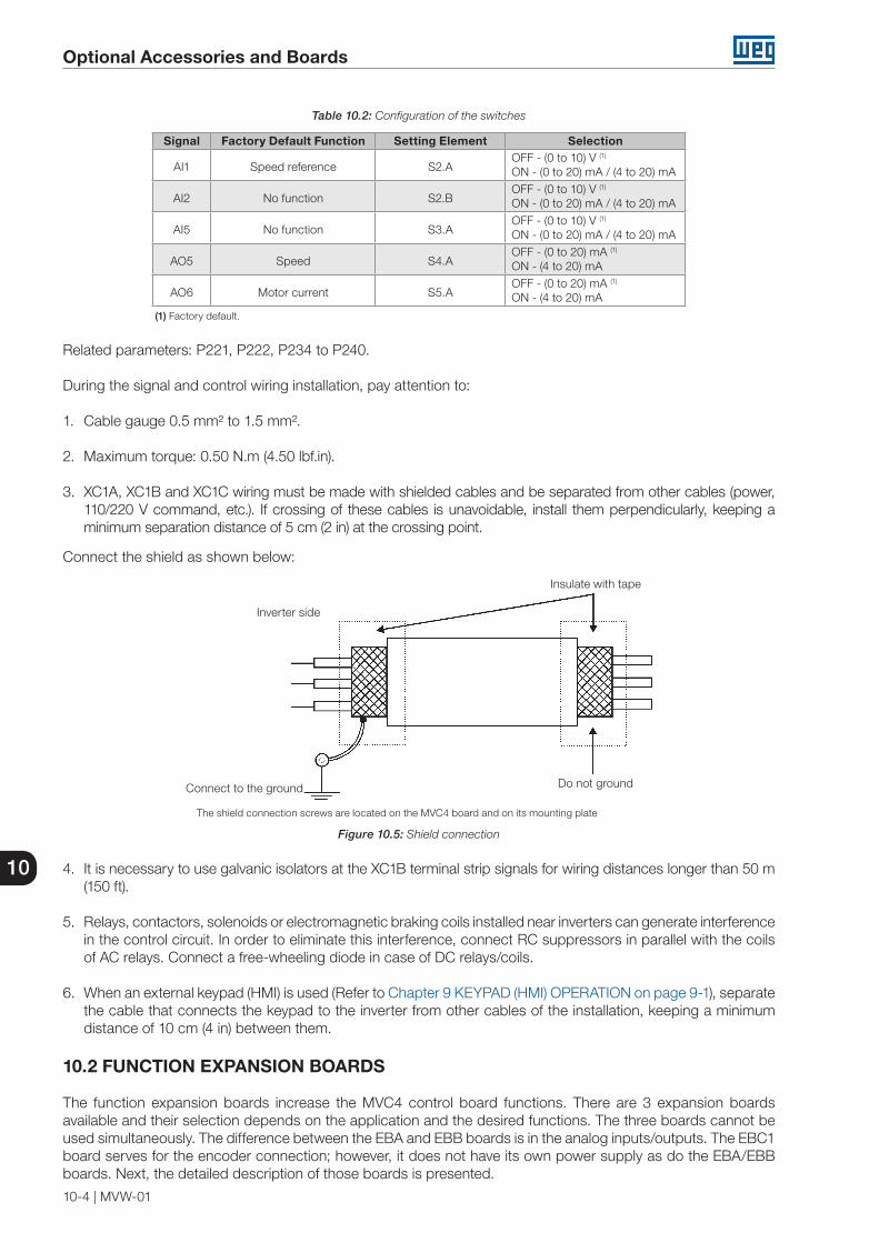
Optional Accessories and Boards
10-4 | MVW-01
10
Table 10.2: Configuration of the switches
Signal Factory Default Function Setting Element Selection
AI1 Speed reference S2.AOFF - (0 to 10) V (1) ON - (0 to 20) mA / (4 to 20) mA
AI2 No function S2.BOFF - (0 to 10) V (1)
ON - (0 to 20) mA / (4 to 20) mA
AI5 No function S3.AOFF - (0 to 10) V (1)
ON - (0 to 20) mA / (4 to 20) mA
AO5 Speed S4.AOFF - (0 to 20) mA (1)
ON - (4 to 20) mA
AO6 Motor current S5.AOFF - (0 to 20) mA (1)
ON - (4 to 20) mA
(1) Factory default.
Related parameters: P221, P222, P234 to P240.
During the signal and control wiring installation, pay attention to:
1. Cable gauge 0.5 mm² to 1.5 mm².
2. Maximum torque: 0.50 N.m (4.50 lbf.in).
3. XC1A, XC1B and XC1C wiring must be made with shielded cables and be separated from other cables (power, 110/220 V command, etc.). If crossing of these cables is unavoidable, install them perpendicularly, keeping a minimum separation distance of 5 cm (2 in) at the crossing point.
Connect the shield as shown below:
The shield connection screws are located on the MVC4 board and on its mounting plate
Insulate with tape
Connect to the ground Do not ground
Inverter side
Figure 10.5: Shield connection
4. It is necessary to use galvanic isolators at the XC1B terminal strip signals for wiring distances longer than 50 m (150 ft).
5. Relays, contactors, solenoids or electromagnetic braking coils installed near inverters can generate interference in the control circuit. In order to eliminate this interference, connect RC suppressors in parallel with the coils of AC relays. Connect a free-wheeling diode in case of DC relays/coils.
6. When an external keypad (HMI) is used (Refer to Chapter 9 KEYPAD (HMI) OPERATION on page 9-1), separate the cable that connects the keypad to the inverter from other cables of the installation, keeping a minimum distance of 10 cm (4 in) between them.
10.2 FUNCTION EXPANSION BOARDS
The function expansion boards increase the MVC4 control board functions. There are 3 expansion boards available and their selection depends on the application and the desired functions. The three boards cannot be used simultaneously. The difference between the EBA and EBB boards is in the analog inputs/outputs. The EBC1 board serves for the encoder connection; however, it does not have its own power supply as do the EBA/EBB boards. Next, the detailed description of those boards is presented.
Optional Accessories and Boards
MVW-01 | 10-5
10
10.2.1 EBA (I/O Expansion Board A)
The EBA board can be supplied in different configurations, created from the combination of specific functions.
The available configurations are shown in the next table.
Table 10.3: EBA board versions and available features
Available FeaturesEBA Board models - Code
EBA.01- A1 EBA.02-A2 EBA.03-A3Differential input for incremental encoder with 12 V / 200 mA isolated internal power supply, feedback for speed regulator, digital speed measurement, 14 bit resolution, 100 kHz maximum signal frequency.
Available Not available Not available
Buffered encoder output signals: isolated input signal repeater, differential output, available to external 5 V to 15 V power supply. Available Not available Not available
Analog differential input (AI4): 14 bits (0.006 % of the full scale range), bipolar: -10 V to +10 V, (0 to 20) mA / (4 to 20) mA programmable. Available Não disponível Available
2 Analog outputs (AO3/AO4): 14 bits (0.006 % of the range [±10 V]), bipolar: -10 V to + 10 V, programmable. Available Not available Available
Isolated RS-485 serial port. Available Available Not availableDigital Input (DI7): isolated, programmable, 24 V. Available Available AvailableDigital Input (DI8) with special function for motor thermistor (PTC): actuation 3.9 kΩ, release 1.6 kΩ. Available Available Available
2 isolated Open Collector transistor outputs (DO1/DO2): 24 V, 50 mA, programmable. Available Available Available
NOTE!The use of the RS-485 serial interface does not allow the use of the standard RS-232 input - they cannot be used simultaneously!
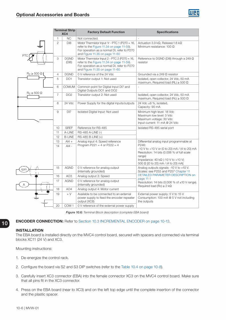
Optional Accessories and Boards
10-6 | MVW-01
10
A
rpm
Rc ≥ 500 Ω
PTC
Rc ≥ 500 Ω
Terminal StripXC4 Factory Default Function Specifications
1 NC Not connected. -
2 DI8 Motor Thermistor Input 1r - PTC 1 (P270 = 16, refer to the Figure 11.34 on page 11-59). For operation as a normal DI, refer to P270 and Figure 11.35 on page 11-60
Actuation 3.9 kΩ, Release:1.6 kΩMinimum resistance: 100 Ω
3 DGND (DI8)
Motor Thermistor Input 2 - PTC 2 (P270 = 16, refer to the Figure 11.34 on page 11-59). For operation as a normal DI, refer to P270 and Figure 11.35 on page 11-60
Reference to DGND (DI8) through a 249 Ωresistor
4 DGND 0 V reference of the 24 Vdc Grounded via a 249 Ω resistor
5 DO1 Transistor output 1: Not used Isolated, open collector, 24 Vdc, 50 mAmaximum, Required load (RL) ≥ 500 Ω
6 COMUM Common point for Digital Input DI7 and Digital Outputs DO1 and DO2
-
7 DO2 Transistor output 2: Not used Isolated, open collector, 24 Vdc, 50 mAmaximum, Required load (Rc) ≥ 500 Ω
8 24 Vdc Power Supply for the digital inputs/outputs 24 Vdc ±8 %, isolated,Capacity: 90 mA
9 DI7 Isolated Digital Input: Not used Minimum high level: 18 VdcMaximum low level: 3 VdcMaximum voltage: 30 VdcInput current: 11 mA @ 24 Vdc
10 SREF Reference for RS-485 Isolated RS-485 serial port
11 A-LINE RS-485 A-LINE (-)
12 B-LINE RS-485 B-LINE (+)
13 AI4 + Analog input 4: Speed referenceProgram P221 = 4 or P222 = 4
Differential analog input programmable at P246:-10 V to +10 V or (0 to 20) mA / (4 to 20) mAResolution: 14 bits (0.006 % of full scale range)Impedance: 40 kΩ (-10 V to +10 V)500 Ω [(0 to 20) mA / (4 to 20) mA]
14 AI4 -
15 AGND 0 V reference for analog output(internally grounded)
Analog outputs signals: -10 V to +10 V.Scales: see P255 and P257 Chapter 11 DETAILED PARAMETER DESCRIPTION on page 11-1Resolution: 14 bits (0.006 % of ±10 V range).Required load (Rc) ≥ 2 kΩ
16 AO3 Analog output 3: Speed
17 AGND 0 V reference for analog output(internally grounded)
18 AO4 Analog output 4: Motor current
19 + V Available to be connected to an external power supply to feed the encoder repeater output (XC8)
External power supply: 5 V to 15 VConsumption: 100 mA @ 5 V not including the outputs
20 COM 1 0 V reference of the external power supply
Figure 10.6: Terminal Block description (complete EBA board)
ENCODER CONNECTION: Refer to Section 10.3 INCREMENTAL ENCODER on page 10-13. INSTALLATIONThe EBA board is installed directly on the MVC4 control board, secured with spacers and connected via terminal blocks XC11 (24 V) and XC3.
Mounting instructions:
1. De-energize the control rack.
2. Configure the board via S2 and S3 DIP switches (refer to the Table 10.4 on page 10-8).
3. Carefully insert XC3 connector (EBA) into the female connector XC3 on the MVC4 control board. Make sure that all pins fit in the XC3 connector.
4. Press on the EBA board (near to XC3) and on the left top edge until the complete insertion of the connector and the plastic spacer.
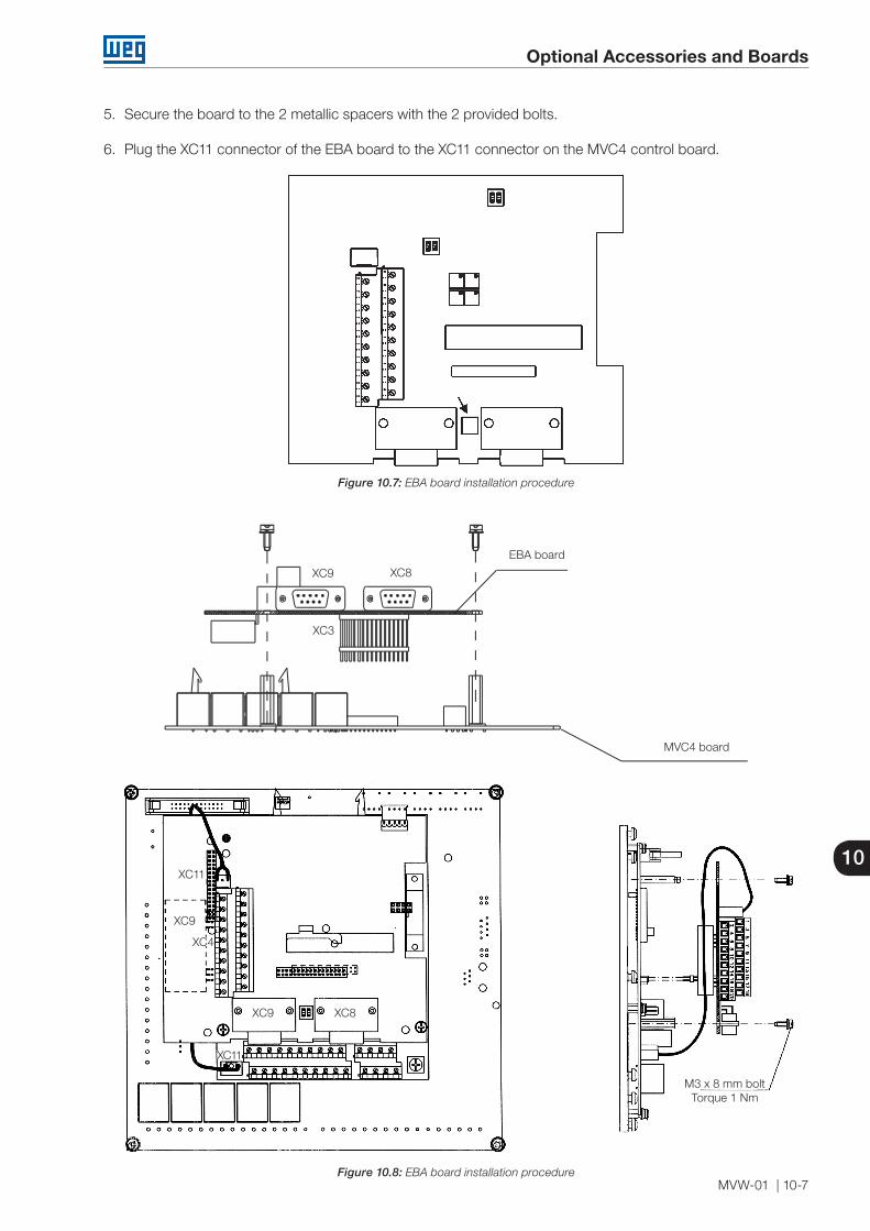
Optional Accessories and Boards
MVW-01 | 10-7
10
5. Secure the board to the 2 metallic spacers with the 2 provided bolts.
6. Plug the XC11 connector of the EBA board to the XC11 connector on the MVC4 control board.
Figure 10.7: EBA board installation procedure
EBA board
MVC4 board
XC9 XC8
XC3
M3 x 8 mm boltTorque 1 Nm
XC9
XC4
XC11
XC11
XC8XC9
Figure 10.8: EBA board installation procedure

Optional Accessories and Boards
10-8 | MVW-01
10
Table 10.4: EBA board configuration of setting elements
Switch Function - Factory Setting OFF (Standard) ONS2.1 Al4 - Speed Reference ( 0 to 10) V (0 to 20) mA or (4 to 20) mAS3.1 RS-485 B - LINE (+)
Without termination With 120 Ω terminationS3.2 RS-485 A - LINE (-)
Note: Both switches, S3.1 and S3.2, must be adjusted for the same option.
Table 10.5: EBA board trimpot configurations
Trimpot Function Factory Default FunctionRA1 AO3 - offset
Motor speedRA2 AO3 - gainRA3 AO4 - offset
Motor currentRA4 AO4 - gain
NOTE!The external signal and control wiring must be connected to XC4 (EBA), following the same recommendations as for the wiring of the MVC4 control board (refer to the Section 10.1 MVC4 SIGNAL AND CONTROL CONNECTIONS on page 10-1).
10.2.2 EBB (I/O Expansion Board B)
The EBB board can be supplied in different configurations, created from the combination of specific functions.
The available functions are presented in the Table 10.6 on page 10-8.
Table 10.6: EBB board versions and available features
Available FeaturesEBB Board Models - Code
EBB.01 B1
EBB.02B2
EBB.03B3
EBB.04B4*
EBB.05B5
Differential input for incremental encoder with 12 V / 200 mA isolated internal power supply, feedback for speed regulator, digital speed measurement, 14 bit resolution, 100 kHz maximum signal frequency.
Available Available Not available Available Not available
Buffered encoder output signals: isolated input signal repeater, differential output, available to external 5 V to 15 V power supply.
Available Not available Not available Available Not available
Analog differential input (AI3): 10 bits (0 to 10) V, (0 to 20) mA / (4 to 20) mA, programmable. Available Not available Available Available Not available
2 Analog outputs (AO1’/AO2’): 11 bits (0.05 % of the full scale range), (0 to 20) mA / (4 to 20) mA, programmable. Available Not available Available Available Available
Isolated RS-485 serial port. Available Not available Not available Available Not available
Digital input (DI7): isolated, programmable, 24 V. Available Available Available Available Not available
Digital input (DI8) with special function for motor thermistor(PTC): actuation 3.9 kΩ, release 1.6 kΩ. Available Available Available Available Not available
2 isolated Open Collector transistor outputs (DO1/DO2):24 V, 50 mA, programmable. Available Available Available Available Not available
* Board with 5 V encoder power supply.
NOTE!The use of the RS-485 serial interface does not allow the use of the standard RS-232 input - theycannot be used simultaneously.The analog outputs AO1’ and AO2’ have the same functions and parameters as AO1 and AO2 onthe MVC4 control board.

Optional Accessories and Boards
MVW-01 | 10-9
10
Rc ≥ 500 Ω
Rc ≥ 500 Ω
TerminalStrip XC5 Factory Default Function Specifications
1 NC Not connected -
2 DI8 Motor thermistor input 1 - PTC 1 (P270 = 16, refer to the Figure 11.34 on page 11-59). For operation as a normal DI, refer to P270 Figure 11.35 on page 11-60
Actuation 3.9 kΩ, Release: 1.6 kΩMinimum resistance: 100 Ω
3 DGND (DI8)
Motor thermistor input 2 - PTC 2 (P270 = 16, refer to the Figure 11.34 on page 11-59). For operation as a normal DI, refer to P270 Figure 11.35 on page 11-60
Reference to DGND (DI8) through a 249 Ω resistor
4 DGND 0 V reference of the 24 Vdc Grounded via a 249 Ω resistor
5 DO1 Transistor output 1: not used Isolated, open collector, 24 Vdc, 50 mAmaximum, Required load (RL) ≥ 500 Ω
6 COMUM Common point for Digital Input DI7 andDigital Outputs DO1 and DO2
-
7 DO2 Transistor output 2: Not used Isolated, open collector, 24 Vdc, 50 mAmaximum, Required load (RL) ≥ 500 Ω
8 24 Vdc Power Supply for the digital inputs/outputs 24 Vdc ±8 %, Isolated,Capacity: 90 mA
9 DI7 Isolated Digital Input: not used Minimum high level: 18 VdcMaximum low level: 3 VdcMaximum voltage: 30 VdcInput current: 11 mA @ 24 Vdc
10 SREF Reference for RS-485 Isolated RS-485 serial port
11 A-LINE RS-485 A-LINE
12 B-LINE RS-485 B-LINE
13 AI3 + Analog input 3: speed referenceProgram P221 = 3 or P222 = 3
Isolated analog input programmable at P243:(0 to 10) V or (0 to 20) mA/(4 to 20) mAResolution: 10 bits (0.1 % of full scale range) Impedance: 400 kΩ (0 to 10) V500 Ω [(0 to 20) mA/(4 to 20) mA]
14 AI3 -
15 AGNDI 0 V reference for analog output(internally grounded)
Isolated analog outputs signals:(0 to 20) mA / (4 to 20) mAScale: Refer to the description of parameters P251 and P253 in Chapter 11 DETAILED PARAMETER DESCRIPTION on page 11-1 (P251 and P253)Resolution: 11 bits (0.5 % of full scale range)Required load ≥ 600 Ω
16 AO1I Analog output 1: speed
17 AGNDI 0 V reference for analog output(internally grounded)
18 AO2I Analog output 2: motor current
19 + V Available to be connected to an externalpower supply to feed the encoder repeater output (XC8)
External power supply: 5 V to 15 VConsumption: 100 mA @ 5 V, not includingthe outputs
20 COM 1 0 V reference of the external power supply
A
rpm
PTC
Figure 10.9: XC5 Terminal Block description (complete EBB board)
ATTENTION!The analog input AI3 and the analog outputs AO1’ and AO2’ isolation has the purpose of interruptingground loops. Do not connect them to high potentials.
ENCODER CONNECTION: refer to Section 10.3 INCREMENTAL ENCODER on page 10-13.
INSTALLATION The EBB board is installed directly on the MVC4 control board, secured with spacers and connected via terminalblocks XC11 (24 V) and XC3.
Mounting instructions:
1. De-energize the control rack.
2. Configure the board via S4, S5, S6 and S7 DIP switches (refer to the Table 10.7 on page 10-11).
3. Carefully insert XC3 connector (EBB) into the female connector XC3 on the MVC4 control board. Make sure that all pins fit in the XC3 connector.
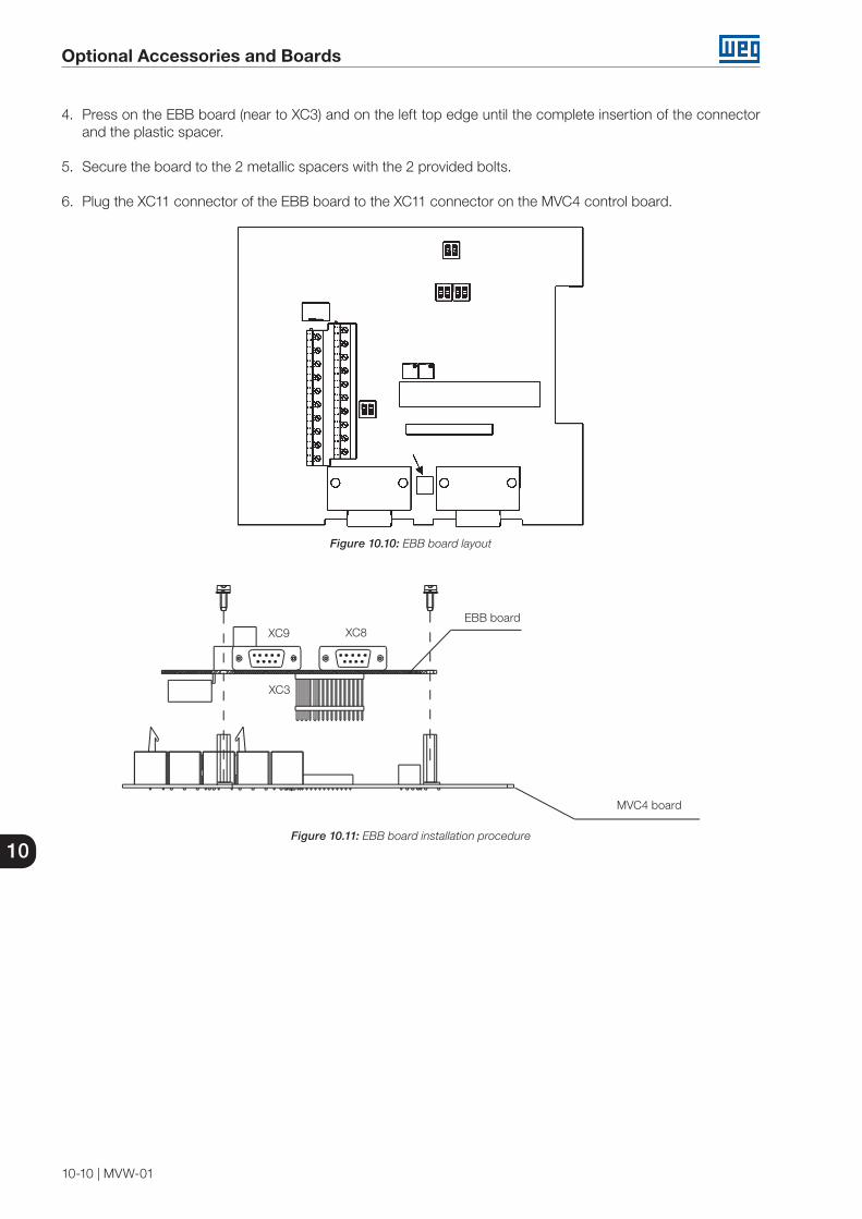
Optional Accessories and Boards
10-10 | MVW-01
10
4. Press on the EBB board (near to XC3) and on the left top edge until the complete insertion of the connector and the plastic spacer.
5. Secure the board to the 2 metallic spacers with the 2 provided bolts.
6. Plug the XC11 connector of the EBB board to the XC11 connector on the MVC4 control board.
Figure 10.10: EBB board layout
EBB board
MVC4 board
XC9 XC8
XC3
Figure 10.11: EBB board installation procedure

Optional Accessories and Boards
MVW-01 | 10-11
10
XC9
XC4
XC11
XC11
XC8XC9
Figure 10.12: EBB board installation procedure
Table 10.7: EBB board DIP switch configurations
Switch Function - Factory Setting OFF ONS4.1 Al3 - Speed Reference ( 0 to 10) V (1) (0 to 20) mA or (4 to 20) mAS5.1 and S5.2 AO1 - Speed
(0 to 20) mA (2) (4 to 20) mA (1)
S6.1 and S6.2 AO2 - Motor CurrentS7.1 and S7.2 RS-485 B - LINE (+)
Without termination (1) With 120 Ω terminationRS-485 A - LINE (-)
(1) Factory default setting. Note: Each group of switches must be set for the same option (ON or OFF). E.g., S6.1 and S6.2 = ON.
(2) When the outputs are set to (0 to 20) mA, it may be necessary to readjust the full scale.
Table 10.8: EBB board trimpot configurations
Trimpot Function Factory Default FunctionRA5 AO1 Full scale adjustment Motor speedRA6 AO2 Full scale adjustment Motor current
NOTE!The external signal and control wiring must be connected to XC5 (EBB), following the same recommendations as for the wiring of the MVC4 control board (refer to the Section 10.1 MVC4 SIGNAL AND CONTROL CONNECTIONS on page 10-1).
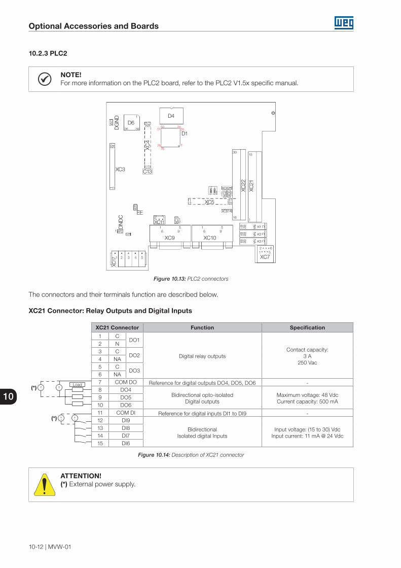
Optional Accessories and Boards
10-12 | MVW-01
10
10.2.3 PLC2
NOTE!For more information on the PLC2 board, refer to the PLC2 V1.5x specific manual.
XC9 XC10
XC7
XC4
XC3
EE
XC5
XC11
XC22
XC21
C13
1 2
1 2
2 1
1 2
3 1
11
2 3 4 5
1
1 562
16
B1
B1
B1
B2
B2
B2
NA
NA
NA
K1
K2
K3
CC
C
30
1
15
6 69 95 5
26
W7
39 51
7576
50 2425
1
1 2
33
34
31 32
33
34D
GN
DD
ND
CD6
D4
D1W
11
XC1
XC2
XC82
XC81
XC6
W12H7
2 1
1
1
1 2
S1 NO
1
XC17
1
Figure 10.13: PLC2 connectors
The connectors and their terminals function are described below.
XC21 Connector: Relay Outputs and Digital Inputs
XC21 Connector Function Specification
1 CDO1
Digital relay outputsContact capacity:
3 A250 Vac
2 N3 C
DO24 NA5 C
DO36 NA7 COM DO Reference for digital outputs DO4, DO5, DO6 -8 DO4
Bidirectional opto-isolatedDigital outputs
Maximum voltage: 48 VdcCurrent capacity: 500 mA
9 DO510 DO611 COM DI Reference for digital inputs DI1 to DI9 -12 DI9
BidirectionalIsolated digital Inputs
Input voltage: (15 to 30) VdcInput current: 11 mA @ 24 Vdc
13 DI814 DI715 DI6
+-
+-
+-
+-
Load(*)
(*)
Figure 10.14: Description of XC21 connector
ATTENTION!(*) External power supply.

Optional Accessories and Boards
MVW-01 | 10-13
10
XC22 Connector: Transistor Outputs and Digital Inputs
XC22 Connector Function Specifications
16 PTC1 Motor thermistor input Actuation: 3.9 kRelease: 1.6 k
Minimum resistance: 100 Ω17 PTC2 PTC
18 GND ENC Reference for the power supply of the encoder input -
19 + ENCEncoder inputpower supply
Controlled 5 Vdc or (8 to 24) VdcCurrent consumption: 50 mA +
Encoders current (**)20 -
AO2 Analog output 2(-10 to +10) Vdc or (0 to 20) mA
12 Bits21 +
22 -AO1 Analog output 1
(-10 to +10) Vdc or (0 to 20) mA12 Bits23 +
24 -AI1
Differential AnalogInput 1
(-10 to +10) Vdc or (-20 to +20) mA14 Bits25 +
26 DI1
Bidirectional, IsolatedDigital Inputs
Input voltage: (15 to 30) VdcInput current: 11 mA @ 24 Vdc
27 DI2
28 DI3
29 DI4
30 DI5+-
+-(*)
COM DI
Figure 10.15: Description of XC22 connector
ATTENTION!(*) External Power supply.(**) For current, the S1 switch must be set ON.
10.3 INCREMENTAL ENCODER
Applications that require more speed or positioning accuracy, a speed feedback of the motor shaft by means of incremental encoder is required. The connection to the inverter is made through the XC9 connector (DB9) on the EBA function expansion board, or XC9 on EBB, or XC10 on EBC.
10.3.1 EBA/EBB Boards
When the EBA or EBB board is used, the selected encoder should have the following characteristics:
Power supply voltage: 12 Vdc, less than 200 mA current consumption.
2 quadrature channels (90º) + zero pulse with complementary outputs (differential):
Signals A, A, B, B, Z and Z.
"Linedriver" or "Push-Pull" output circuit type (12 V level).
Electronic circuit isolated from the encoder frame.
Recommended number of pulses per revolution: 1024 ppr.
Follow the recommendations bellow when mounting the encoder on the motor:
Couple the encoder directly to the motor shaft (use a flexible coupling without torsional flexibility).
Both the shaft and the metallic frame of the encoder must be electrically isolated from the motor (3 mm (0.119 in) minimum distance).
Use high quality flexible couplings to prevent mechanical oscillation or backlash.

Optional Accessories and Boards
10-14 | MVW-01
10
The electrical connections must be made with shielded cable, maintaining a minimum distance of about 25 cm (10 in) from other wires (power, control cables, etc.). If possible, install the encoder cable in a metallic conduit.
During the commissioning, it is necessary to program the control type, P202 = 4 (Vector with encoder), in order to operate with speed feedback via incremental encoder.
Refer to the Chapter 11 DETAILED PARAMETER DESCRIPTION on page 11-1 for more details on vector control.
The function expansion boards EBA and EBB have an encoder signal repeater, isolated and externally powered.
(1) Power supply voltage 12 Vdc / 220 mA for encoder.(2) Referenced to ground via 1 μF in parallel with 1 kΩ.(3) Connector pinout valid for HS35B Dynapar encoder. For other encoder models, verify the correct connection in order to meet the required sequence.
XC9 connector (Male DB9)
red
blueyellow
green
pinkwhite
brown
gray
cable shield
12 Vdifferential(88C20)
Encoder
Maximum recommended length: 100 m (300 ft)
MVW-01 EBA or EBB board
Connector Encoder (3)
A A
H A
B B
I B
C Z
J Z
D +VE
F COM
E NC
G
Connector XC9 Description
3 A
2 A Encoder Signals
1 B
9 B
8 Z
7 Z 4 +VE Power supply (1)
6 COM 0 V reference (2)
5 Ground
Figure 10.16: Encoder input
NOTE!The maximum allowed encoder signal frequency is 100 kHz.
Sequence of the encoder signals:
Motor running in forward direction
B t
A t
Figure 10.17: Encoder signals
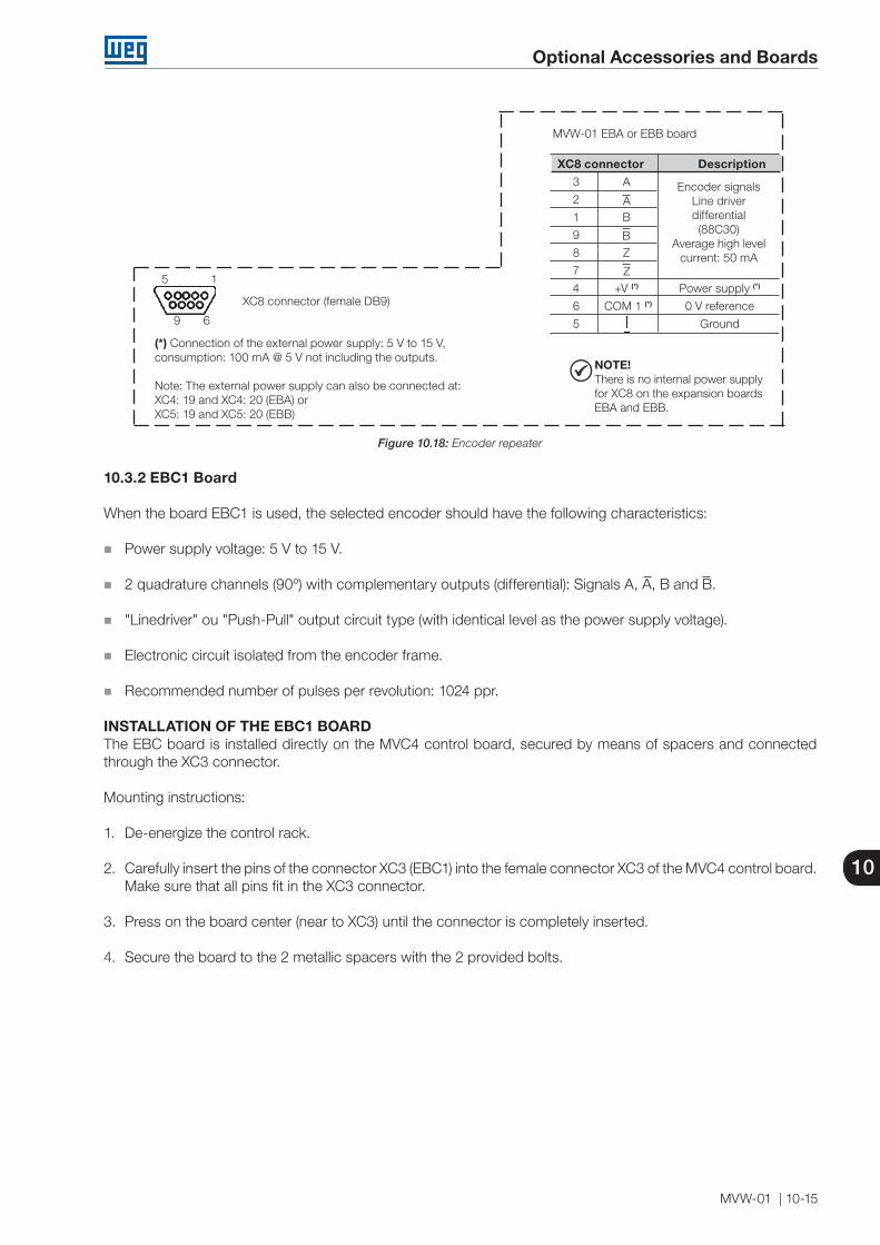
Optional Accessories and Boards
MVW-01 | 10-15
10
XC8 connector (female DB9)
(*) Connection of the external power supply: 5 V to 15 V,consumption: 100 mA @ 5 V not including the outputs.
Note: The external power supply can also be connected at:XC4: 19 and XC4: 20 (EBA) orXC5: 19 and XC5: 20 (EBB)
MVW-01 EBA or EBB board
9 6
5 1
NOTE!There is no internal power supplyfor XC8 on the expansion boardsEBA and EBB.
XC8 connector Description 3 A
2 A
1 B
9 B
8 Z
7 Z
4 +V (*) Power supply (*)
6 COM 1 (*) 0 V reference
5 Ground
Encoder signalsLine driverdifferential(88C30)
Average high levelcurrent: 50 mA
Figure 10.18: Encoder repeater
10.3.2 EBC1 Board
When the board EBC1 is used, the selected encoder should have the following characteristics:
Power supply voltage: 5 V to 15 V.
2 quadrature channels (90º) with complementary outputs (differential): Signals A, A, B and B.
"Linedriver" ou "Push-Pull" output circuit type (with identical level as the power supply voltage).
Electronic circuit isolated from the encoder frame.
Recommended number of pulses per revolution: 1024 ppr.
INSTALLATION OF THE EBC1 BOARDThe EBC board is installed directly on the MVC4 control board, secured by means of spacers and connected through the XC3 connector.
Mounting instructions:
1. De-energize the control rack.
2. Carefully insert the pins of the connector XC3 (EBC1) into the female connector XC3 of the MVC4 control board. Make sure that all pins fit in the XC3 connector.
3. Press on the board center (near to XC3) until the connector is completely inserted.
4. Secure the board to the 2 metallic spacers with the 2 provided bolts.
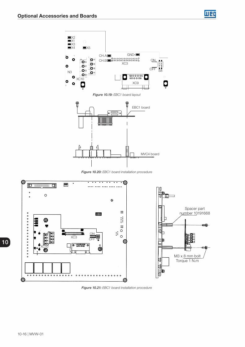
Optional Accessories and Boards
10-16 | MVW-01
10
X5
X2X1X3
N3
X4
ON
OFF
CH.A GND*
CH.B
S8
XC10
XC3
XC9
Figure 10.19: EBC1 board layout
EBC1 board
MVC4 board
Figure 10.20: EBC1 board installation procedure
M3 x 8 mm boltTorque 1 N.m
Spacer partnumber 10191668
ON
OFF
XC10
XC3
XC9
Figure 10.21: EBC1 board installation procedure

Optional Accessories and Boards
MVW-01 | 10-17
10
CONFIGURATIONS:Table 10.9: EBC1 board configurations
Expansion Board Power Supply Encoder Voltage Necessary Setting
EBC1.01External 5 V 5 V
Commutate switch S8 to ON, see Figure 10.19 on page 10-16
External 8 V to 15 V 8 V to 15 V NoneEBC1.02 Internal 5 V 5 V NoneEBC1.03 Internal 12 V 12 V None
NOTE!The terminals XC10:22 and XC10:23 (see Figure 10.19 on page 10-16), should only be used for encoder supply, when the encoder power supply is not coming from the DB9 connector.
ENCODER MOUNTING:
Follow the recommendations bellow when mounting the encoder on the motor:
Couple the encoder directly to the motor shaft (use a flexible coupling without torsional flexibility).
Both the shaft and the metallic frame of the encoder must be electrically isolated from the motor (3 mm (0.119 in) minimum distance.
Use high quality flexible couplings to prevent mechanical oscillation or backlash.
The electrical connections must be made with shielded cable, maintaining a minimum distance of about 25 cm (10 in) from other wires (power, control cables, etc.). If possible, install the encoder cable in a metallic conduit.
During the commissioning, it is necessary to program the control type, P202 = 4 (Vector with encoder), in order to operate with speed feedback via incremental encoder.
Refer to the Chapter 11 DETAILED PARAMETER DESCRIPTION on page 11-1 for more details on vector control.
(1) External encoder power supply: 5 to 15 Vdc. Consumption of 40 mA plus the encoder consumption.(2) 0 V reference of the power supply voltage.(3) Connector pinout valid for HS35B Dynapar encoder. For other encoder models, verify the correct connection in order to meet the required sequence.
Conector XC9 (DB9 - Macho)Comprimento máximo recomendado: 100m
XC9 connector (Male DB9)
red
blueyellow
green
whitebrown
cable shield
Encoder
Maximum recommended length: 100 m (300 ft)
MVW-01 EBC board
Encoder connector (3)
A A
H A
B B
I B C Z
J Z D +VE F COM E NC G
Connectors Signal Description
XC9 XC10
3 26 A
2 25 A Encoder Signals
1 28 B (5 to 15 V)
9 27 B
8 Z
7 Z 4 21,22 +VE Power supply (1)
6 23,24 COM 0 V reference (2)
5 Ground
Figure 10.22: EBC1 encoder input
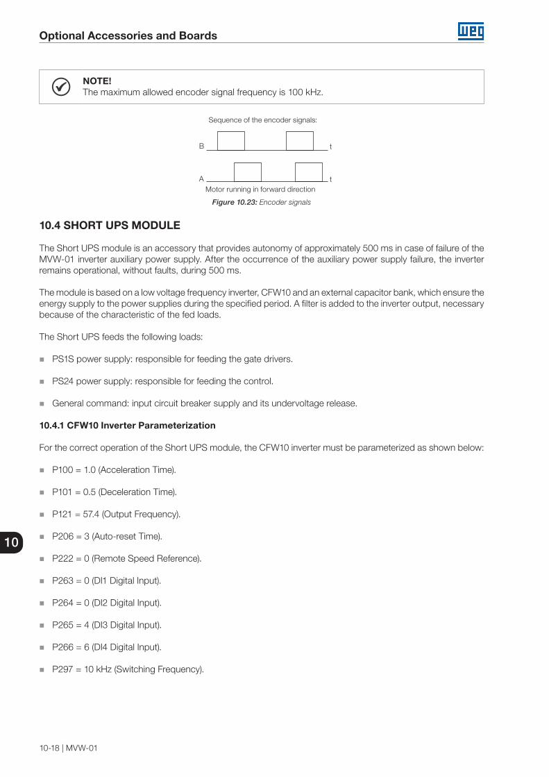
Optional Accessories and Boards
10-18 | MVW-01
10
NOTE!The maximum allowed encoder signal frequency is 100 kHz.
Sequence of the encoder signals:
Motor running in forward direction
B t
A t
Figure 10.23: Encoder signals
10.4 SHORT UPS MODULE
The Short UPS module is an accessory that provides autonomy of approximately 500 ms in case of failure of the MVW-01 inverter auxiliary power supply. After the occurrence of the auxiliary power supply failure, the inverter remains operational, without faults, during 500 ms.
The module is based on a low voltage frequency inverter, CFW10 and an external capacitor bank, which ensure the energy supply to the power supplies during the specified period. A filter is added to the inverter output, necessary because of the characteristic of the fed loads.
The Short UPS feeds the following loads:
PS1S power supply: responsible for feeding the gate drivers.
PS24 power supply: responsible for feeding the control.
General command: input circuit breaker supply and its undervoltage release.
10.4.1 CFW10 Inverter Parameterization
For the correct operation of the Short UPS module, the CFW10 inverter must be parameterized as shown below:
P100 = 1.0 (Acceleration Time).
P101 = 0.5 (Deceleration Time).
P121 = 57.4 (Output Frequency).
P206 = 3 (Auto-reset Time).
P222 = 0 (Remote Speed Reference).
P263 = 0 (DI1 Digital Input).
P264 = 0 (DI2 Digital Input).
P265 = 4 (DI3 Digital Input).
P266 = 6 (DI4 Digital Input).
P297 = 10 kHz (Switching Frequency).
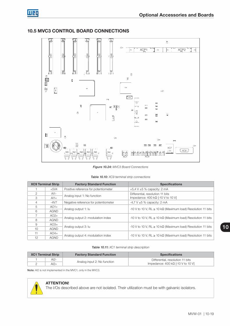
Optional Accessories and Boards
MVW-01 | 10-19
10
10.5 MVC3 CONTROL BOARD CONNECTIONS
XCP2
XC8XC7
XC9XC1
XC3
N5 N2 N8 N3 N6 N4
XCP1C
N1
CN
2
CN
3
CN
4
CN
5
CN
6
Figure 10.24: MVC3 Board Connections
Table 10.10: XC9 terminal strip connections
XC9 Terminal Strip Factory Standard Function Specifications
1 +5V4 Positive reference for potentiometer +5,4 V ±5 % capacity: 2 mA2 AI1-
Analog input 1: No functionDifferential, resolution 11 bitsImpedance: 400 kΩ [-10 V to 10 V]3 AI1+
4 -4V7 Negative reference for potentiometer -4,7 V ±5 % capacity: 2 mA5 AO1+
Analog output 1: Iu -10 V to 10 V, RL ≥ 10 kΩ (Maximum load) Resolution 11 bits6 AGND7 AO2+
Analog output 2: modulation index -10 V to 10 V, RL ≥ 10 kΩ (Maximum load) Resolution 11 bits8 AGND9 AO3+
Analog output 3: Iu -10 V to 10 V, RL ≥ 10 kΩ (Maximum load) Resolution 11 bits10 AGND11 AO4+
Analog output 4: modulation index -10 V to 10 V, RL ≥ 10 kΩ (Maximum load) Resolution 11 bits12 AGND
Table 10.11: XC1 terminal strip description
XC1 Terminal Strip Factory Standard Function Specifications
1 AI2-Analog input 2: No function
Differential, resolution 11 bitsImpedance: 400 kΩ [-10 V to 10 V]2 AI2+
Note: AI2 is not implemented in the MVC1, only in the MVC3.
ATTENTION!The I/Os described above are not isolated. Their utilization must be with galvanic isolators.

Optional Accessories and Boards
10-20 | MVW-01
10
Detailed Parameter Description
MVW-01 | 11-1
11
11 DETAILED PARAMETER DESCRIPTION
This chapter describes in detail all the parameters of the inverter. In order to simplify the explanation, the parameters have been grouped by characteristics and functions:
Read-only Parameters. Variables that can be viewed on the display but cannot be changed by the user.Regulation Parameters. Programmable values used by the inverter functions.Configuration Parameters. They define the inverter characteristics, the functions to be executed, as well as
the control board I/O functions.Motor Parameters. Used motor data, consisting of information from the motor nameplate.Special Function Parameters. It includes parameters related to special functions.
Symbols and definitions used in the following text:(1) Parameter can be changed only with the inverter disabled (motor stopped).(2) Values may change as a function of the motor parameters.(3) Values may change as a function of P412 (Tr Constant).(4) Values may change as a function of P296.(5) Values may change as a function of P295.(6) Values may change as a function of P320.
Torque current = is the total motor current component responsible for the torque development (in vector control mode).
Active current = is the total motor current component proportional to the active electric power consumed by the motor (in V/F control mode).
11.1 ACCESS AND READ ONLY PARAMETERS - P000 TO P099
ParameterRange
[Factory Setting]Unit
Description/Notes
P000AccessParameter/PasswordSetting
For safety reasons, it will only be possible to change the password with the service HMI, which accompanies the product.
0 to 999[ 0 ]
-
It allows the parameter contents modification. With the parameters adjusted according to the factory default [P200 = 1 (Active password)], it is necessary to program P000 = 5 in order to be able to change the parameter contents, i.e., the password is 5.
To change the password to another value (Password 1) proceed as follows:
1. Adjust P000 = 5 (current password) and P200 = 0 (Inactive password).
2. Press the key.3. Change P200 to 1 (Active password).4. Press again: the display shows P000.
5. Press again: the display shows 5 (current password value).
6. Adjust the new password (Password 1) with the and keys.7. Press : the display shows P000. From this moment on the
value adjusted above becomes the new password (Password 1). Therefore, in order to change parameters it will be necessary to program P000 = the new password (Password 1).
Detailed Parameter Description
11-2 | MVW-01
11
ParameterRange
[Factory Setting]Unit
Description/Notes
P001Speed Reference
P133 to P134[ - ]
1 rpm
Speed reference value presented in rpm (factory default). Regardless of the reference source. The displayed unit can be changed by means of P208 and P210.
P002Motor Speed
0 to P134[ - ]
1 rpm
It shows the motor speed in rpm (with a 0.5 s filter). The displayed unit can be changed by means of P208 and
P210.
P003Motor Current
0 to 3705[ - ]
0.1 A(<1000)-1 A(≥ 1000)
It indicates the inverter output current in Amperes (A). The current is calculated as a function of the motor torque and
speed. When P621 > 0 (sinusoidal filter), the motor current is estimated
as a function of the sinusoidal filter. With P621 > 0 the current measured in the inverter output can
be seen in P011. It has Output Current Filter, P139. Default value P139 = 0.2 s. For line 2 x D and 2 x E, the HMI of the master rack indicates
the sum of the currents of the slave inverters, and the HMIs of the slave racks indicate the current supplied to the motor for each inverter.
P004DC Link Voltage
0 to 8000[ - ]1 V
It shows the DC link actual voltage in Volts (V). P004 is equal to the addition of P052 and P053 values. For line 2 x D and 2 x E, the HMI of the master rack indicates the
highest voltage among the DC link of the slaves. The HMI of the slaves shows the present voltage on the DC link of each inverter.
P005Motor Frequency
0.0 to 300.0[ - ]
0.1 Hz
Inverter output frequency value in Hertz (Hz).
P006Inverter Status
0 to 28[ - ]-
It indicates the current inverter status according to the status machine diagram presented in the Figure 11.1 on page 11-4.
Inverter possible states:0 = ‘Booting’ indicates that the control board is waiting for the initialization end.1 = ‘Sub’ indicates that the inverter has insufficient voltage for operation (undervoltage), and does not accept the enabling command (inverter waiting for the pre-charge/power energization command).2 = ‘Inv. Ready’ indicates that the inverter is ready to be enabled.3 = ‘Motor Mag.’ indicates that the motor is being magnetized by DCcurrent. This state lasts for two times the motor rotoric constant time(P412).4 = ‘Motor Rdy.’ indicates that the motor is magnetized and the inverter is waiting for the run command.5 = ‘Up Ramp’ indicates the motor is in the speed acceleration ramp.6 = ‘Down Ramp’ indicates that the motor is in the speed deceleration ramp.7 = ‘In Ref.’ indicates that the motor is rotating at the adjusted speedreference.8 = ‘DC Break’ indicates that the motor is stopping with DC braking.
Detailed Parameter Description
MVW-01 | 11-3
11
ParameterRange
[Factory Setting]Unit
Description/Notes
9 = ‘Coast‘ indicates that the motor is coasting, without being driven by the inverter.10 = ‘Ride Thro.’ indicates that the inverter is operating during momentary line faults.11 = ‘Flying St.’ indicates that the inverter has received a command to start a spinning motor. This state persists until the inverter reaches the motor speed.12 = ‘Test Mode’ indicates that the inverter is in a transitory state to test mode or to self-tuning.13 = ‘Inv. Test’ indicates that the inverter is in a general test state.14 = ‘Self-Comm.’ Indicates that the inverter is performing the self-tuning, automatically measuring motor parameters.15 = ‘Power Test’ indicates that the inverter is testing power cabinetspecific processes. 16 = Fault.17 = Alarm.18 = ‘Calibrat.’ indicates that the inverter is in the feedback signalcalibration process.19 = ‘Hold’ indicates that the inverter is in DC link regulation mode. Refer to the parameter P151 description.20 = ‘I Limit’ indicates that the inverter is in current limitation. Refer to the parameter P169 description.21 = ‘I Fast Limit’ indicates that the inverter is in fast current limitation.22 = ‘Ride Thr 2’ indicates Ride-Through without interruption.The state machine diagram can be seen in the Figure 11.1 on page 11-4, where the states indicated from 1 to 22 have their possible transitions indicated by the state changing arrows.23 = ‘Hold 2’. 24 = ‘Sync’ indicates that the inverter is synchronized with the line.25 = ‘Fast Disab’ indicates fast disable mode (HG = off) fast (MVC3).26 = ‘In Sync’ indicates that the inverter is trying to synchronize with the line.27 = ‘Safety’: indicates the inverter is in the safe stop mode.28 = ‘WaitComm’: indicates the inverter is waiting for communication between master and slaves.
NOTE!States that are not transitory, that is, states in which the inverter may remain for an undetermined period, are identified with an arrow that indicates the LOOP condition .

Detailed Parameter Description
11-4 | MVW-01
11
Wait-Boot Wait ComSafety
SUB
Inverterready
Test mode
Invertertest mode
Power stagetest mode
Selfcom.
Motor mag.
Motor RDY
Current limit
Down ramp
DC break CoastUp ramp
Hold
HoldIn refRide
trough
Insync
Rastdisab.Sync
Flying start
Calibration
Current fast limit
15
DI27 280
1
2
3
4
18
12 13
14
11
10 7 19 21
5 20 6 8 9
(1)
(1)
Ride 2
22
23
2324
25
Figure 11.1: State machine
ParameterRange
[Factory Setting]Unit
Description/Notes
P007Motor Voltage
0 to 8000[ - ]1 V
It indicates the inverter output voltage in Volts (V), based on the voltage and modulation index of the DC link.
P009Motor Torque
0.0 to 250.0[ - ]
0.1 %
It indicates the torque developed by the motor, calculated in the following way:
P009 = Itm x 100 Itm nominalWhere:Itm = Actual motor torque current.
Vector Mode:Itm nominal
= Motor nominal torque current.
Scalar Mode:Itm nominal
= Inverter nominal torque current.
Detailed Parameter Description
MVW-01 | 11-5
11
ParameterRange
[Factory Setting]Unit
Description/Notes
P010Output Power
0 to 9999[ - ]
1 kW
It indicates the inverter instantaneous output power in kW.
P011Inverter Current
Parameter only visible with P621 = 1, 2 (sinusoidal filter active)
0 to 2600[ - ]
0.1 A(<1000)-1 A(≤ 1000)
It indicates the inverter output current, in ampères.
P012Digital Inputs Status DI1 to DI10(MVC4 andoptional board)
A = Active I = Inactive
[ - ] -
It indicates, on the HMIG, the state of the eight digital inputs of the control board MVC4 (DI1 to DI6, DI9, DI10) and of the two digital inputs of the optional board (DI7, DI8), by means of letters A (Active) and I (Inactive), in the following order:
DI1, DI2, ... ,DI7, DI8, DI9, DI10
Detailed Parameter Description
11-6 | MVW-01
11
ParameterRange
[Factory Setting]Unit
Description/Notes
P013Digital Outputs StatusDO1, DO2 and Relays RL1, RL2, RL3, RL4 and RL5 (MVC4 and optional board)
A = Active I = Inactive
[ - ]-
It indicates, on the IHMG, the state of the two digital outputs of the optional board, (DO1, DO2) and of the five relay outputs of the control board MVC4 by means of the numbers 1 (Active) and 0 (Inactive) in the following order:
DO1, DO2, RL1, RL2, RL3, RL4, RL5.
P014Last Error
P015Second Error
P016Third Error
P017Fourth Error
0 to 255[ - ]-
0 to 255[ - ]-
0 to 255[ - ]-
0 to 255[ - ]-
They indicate, respectively, the codes of the last, last but one, last but two and last but three error occurred.
Recording sequence:
Error → P014 → P015 → P016 → P017 → P060 → P061 → P062 → P063 → P064 → P065.
To access more information about the error occurred, P067.
P018Analog Input AI1’ (MVC4 board)
P019Analog Input AI2’ (MVC4 board)
P020Analog Input AI3’(EBB board))
P021Analog Input AI4’ (EBA board)
0.0 to 100.0[ - ]
0.1 %
-100.0 to +100.0[ - ]
0.1 %
-100.0 to +100.0[ - ]
0.1 %
-100.0 to +100.0[ - ]
0.1 %
They present the MVC4 control board analog inputs AI1 and AI2, EBB board AI3 and EBA board AI4 values, as a full scale percentage. The indicated values are those obtained after offset action and gain multiplication. Refer to the parameters P234 to P247 description. The analog input AI2 has a filter that differentiates it from the others (refer to P248).
P022MVC3 BoardTemperature
0 to 100[ - ]1 °C
It indicates the MVC3 control board temperature, in Celsius degrees.
P023MVC4 SoftwareVersion
XX.X[ - ]-
It indicates the software version contained in the MVC4 microcontroller memory.
P024Value of the A/D Conversion of Analog Input AI4 (optional board)
LCD = -32768 to +32767
LED = 0 to FFFFH[ - ]-
It indicates the analog input AI4, which is located in the optional board, A/D conversion result.
The HMI LCD indicates the conversion result in decimal, and the LED display in hexadecimal with negative values in two’s complement.

Detailed Parameter Description
MVW-01 | 11-7
11
ParameterRange
[Factory Setting]Unit
Description/Notes
P025Iv Current A/DConversion Value
P026lw Current A/D Conversion Value
P027Iu Current A/DConversion Value
0 to 4095[ - ]-
0 to 4095[ - ]-
0 to 4095[ - ]-
P025, P026 and P027 indicate, respectively, the result of the A/D conversion, in module, of the phase currents V, W and U.
P028Analog Input AI5’ (MVC4 board)
0.0 to 100.0[ - ]
0.1 %
It presents the MVC4 control board analog input AI5 value as a full scale percentage. The indicated value is obtained after offset action and gain multiplication. Refer to the parameters P721 to P724 description.
P029Trace FunctionStatus
0 to 3[ 0 ]
-
It indicates the state of the trace function. When trace is completed, as you press the key , the date
and time at the moment of the trigger is presented.
Table 11.1: Trace function status
P029 Function0 Inactive1 Waiting for trigger2 Trigger occurred3 Trace completed
Detailed Parameter Description
11-8 | MVW-01
11
ParameterRange
[Factory Setting]Unit
Description/Notes
P030Temperature Register CH1
P031Temperature Register CH2
P032Temperature Register CH3
P033Temperature Register CH4
P034Temperature Register CH5
P035Temperature Register CH6
P036Temperature Register CH7
P037Temperature Register CH8
Theseparameters areonly visible on thedisplay when P315 = 1 (Tecsystem) or P315 = 2 (Pextron)
0 to 240[ - ]1 oC
0 to 240[ - ]1 °C
0 to 240[ - ]1 °C
0 to 240[ - ]1 °C
0 to 240[ - ]1 °C
0 to 240[ - ]1 °C
0 to 240[ - ]1 °C
0 to 240[ - ]1 °C
For these parameters to indicate the motor temperatures properly, the temperature control module (Tecsystem, Pextron) must be installed observing the recommendation contained in its manual.
The communication between the Tecsystem and the MVW-01 control boards occurs through the Tecsystem-Busmod module and the MVC3 SCI1 serial channel. The parameter P315 must be programmed so that the SCI1 channel be used with the Tecsystem module (P315 = 1) or Pextron (P315 = 2).
The overtemperature fault and alarm levels are directly configured on the temperature control module according to its manual.
The configuration of serial transmission of the module must be set as follows:Tecsystem:Baud rate: 19200 bps (SW1.dip1 = 1 / SW1.dip2 = 1).Parity: Even (SW1.dip3 = 1 / SW1.dip4 = 1).Slave address: 1 (SW2.dip7 to dip1 = 0 / SW2.dip0 = 1).Pextron:Baud rate: 19200 bps (P028 = 19.2).Parity: Even (P030 = 2).Slave address: 1 (P029 = 1).
P040PID ProcessVariable
Theseparameters areonly visible on thedisplay whenP203 = 1 or 3
0 to P528[ - ]%
It indicates, in percentage (factory default), the process variable used as the PID feedback.
The variable unit can be changed through the parameters P530, P531 and P532. The scale can be changed through P528 and P529.
Refer to the detailed description at Section 12.2 PID Regulator on page 12-6.
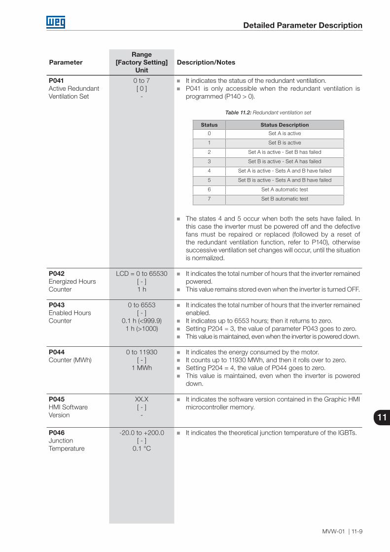
Detailed Parameter Description
MVW-01 | 11-9
11
ParameterRange
[Factory Setting]Unit
Description/Notes
P041Active RedundantVentilation Set
0 to 7[ 0 ]
-
It indicates the status of the redundant ventilation. P041 is only accessible when the redundant ventilation is
programmed (P140 > 0).
Table 11.2: Redundant ventilation set
Status Status Description
0 Set A is active
1 Set B is active
2 Set A is active - Set B has failed
3 Set B is active - Set A has failed
4 Set A is active - Sets A and B have failed
5 Set B is active - Sets A and B have failed
6 Set A automatic test
7 Set B automatic test
The states 4 and 5 occur when both the sets have failed. In this case the inverter must be powered off and the defective fans must be repaired or replaced (followed by a reset of the redundant ventilation function, refer to P140), otherwise successive ventilation set changes will occur, until the situation is normalized.
P042Energized Hours Counter
LCD = 0 to 65530[ - ]1 h
It indicates the total number of hours that the inverter remained powered.
This value remains stored even when the inverter is turned OFF.
P043Enabled Hours Counter
0 to 6553[ - ]
0.1 h (<999.9)1 h (>1000)
It indicates the total number of hours that the inverter remained enabled.
It indicates up to 6553 hours; then it returns to zero. Setting P204 = 3, the value of parameter P043 goes to zero. This value is maintained, even when the inverter is powered down.
P044Counter (MWh)
0 to 11930[ - ]
1 MWh
It indicates the energy consumed by the motor. It counts up to 11930 MWh, and then it rolls over to zero. Setting P204 = 4, the value of P044 goes to zero. This value is maintained, even when the inverter is powered
down.
P045HMI SoftwareVersion
XX.X[ - ]-
It indicates the software version contained in the Graphic HMI microcontroller memory.
P046JunctionTemperature
-20.0 to +200.0[ - ]
0.1 °C
It indicates the theoretical junction temperature of the IGBTs.

Detailed Parameter Description
11-10 | MVW-01
11
ParameterRange
[Factory Setting]Unit
Description/Notes
P047Temperature on the Power Arm of Phase U of Parallel Inverter A
P048Temperature on the Power Arm of Phase V of Parallel Inverter A
P049Temperature on the Power Arm of Phase W of Parallel Inverter A
-20.0 to +200.0[ - ]
0.1 ºC
-20 to +200.0[ - ]
0.1 ºC
-20 to +200.0[ - ]
0.1 ºC
P047, P048 and P049 indicate, respectively, the temperature, in degrees Celsius, on the power arm of phases U, V and W of the parallel inverter A.
P050Temperature on the Arm of the Braking Circuit of Parallel Inverter A
-20.0 to +200.0[ - ]
0.1 ºC
It indicates the temperature on the arm of the braking circuit in degrees Celsius.
When the braking circuit (optional) does not exist, parameter P050 indicates 0.0 ºC.
P051Temperature on the Parallel Rectifier
-20.0 to +200.0[ - ]
0.1 ºC
It indicates the temperature on the heatsink of the input rectifier in degrees Celsius.
P052Negative DC LinkVoltage
0 to 8000[ - ]1 V
It indicates the positive DC link actual voltage, in Volts.
P053Positive DC LinkVoltage
0 to 8000[ - ]1 V
It indicates the positive DC link actual voltage, in Volts.
P055Temperature on the Power Arm of Phase U
P056Temperature on the Power Arm of Phase V
P057Temperature on the Power Arm of Phase W
-20.0 to +200.0[ - ]
0.1 °C
-20.0 to +200.0[ - ]
0.1 °C
-20.0 to +200.0[ - ]
0.1 °C
P055, P056 and P057 indicate, respectively, the temperature in Celsius degrees at the power arms of the phases U, V and W.

Detailed Parameter Description
MVW-01 | 11-11
11
ParameterRange
[Factory Setting]Unit
Description/Notes
P058Temperature on the Arm of the Braking Circuit
-20.0 to +200.0[ - ]
0.1 °C
It indicates the braking arm temperature, in Celsius degrees. When the braking arm (optional) is not present, P058 shows
0.0 °C.
P059Rectifier 1Temperature(standard)
-20.0 to +200.0[ - ]
0.1 °C
It indicates the input rectifier heatsink temperature, in Celsius degrees.
P060Fifth Error
P061Sixth Error
P062Seventh Error
P063Eighth Error
P064Ninth Error
P065Tenth Error
0 to 255[ - ]-
0 to 255[ - ]-
0 to 255[ - ]-
0 to 255[ - ]-
0 to 255[ - ]-
0 to 255[ - ]-
These parameters indicate the error code of the fifth, sixth, seventh, eighth, ninth and tenth errors, respectively.
Recording sequence:
Error → P014 → P015 → P016 → P017 → P060 → P061 → P062 → P063 → P064 → P065.
To access more information about the error occurred, see P067.
P066Software Version of the Board MVC3
XX.X[ - ]-
It indicates the software version contained in the microcontroller memory located on the control board MVC3.
P067Error Log
1 to 100[ - ]-
It keeps the record of the last 100 errors (alarms/faults) occurred in the inverter.
To access the error log, press the key and then use the and keys to change the indication of the corresponding error. The last error occurred (the most recent error event) is represented by the error register 1, and the hundredth error occurred (the oldest error event) is represented by register 100. The information presented in the register includes the error number (e.g. A/F 087), the inverter state at the moment of the error (e.g.: Inv. Ready) and date/time at the moment the error occurred.For instance, in order to access the 8th last occurred error, proceed in the following manner:
Access the parameter P067. Press the key. Use the and keys to access the eighth record.

Detailed Parameter Description
11-12 | MVW-01
11
ParameterRange
[Factory Setting]Unit
Description/Notes
P070Digital Input Status DI1 to DI16 (MVC3 board)
A = ActiveI = Inactive
[ - ]-
It indicates on the HMIG the state of the 16 digital inputs of the control board MVC3 (DI1 to DI16), and the state of each input is considered a bit, in the following order:
DI1, DI2, ... , DI15, DI16.
P071Relay Output StatusRL1 to RL8 (MVC3board)
A = ActiveI = Inactive
[ - ]-
It indicates on the HMIG the state of the 8 relay outputs of the control board MVC3, and the state of each input is considered a bit, in the following order:
RL1, RL2, ... , RL7, RL8.
P072Vab Input Voltage(sinusoidal signal)
-8000 to +8000[ - ]
1 Vac
It indicates the line voltage between phases a and b (Vab) at the input inverter, in Volts.
P073Vcb Input Voltage(sinusoidal signal)
-8000 to +8000[ - ]
1 Vac
It indicates the line voltage between phases c and b (Vcb) at the input inverter, in Volts.
P074Voltage Modulus of Input Transformer Secondary
0 to 3750[ - ]
1 Vac
It indicates the voltage modulus of the input transformer secondary star winding, in Volts.
P075Medium Point to Ground Voltage
0.0 to 100.0[ - ]
0.1 %
It indicates the voltage between the DC link medium point (PM) and the ground (GND), in %.Note: 100 % is equivalent to the line voltage of the an input ransformer secondary winding. Except for modules with 18-pulse rectifier or line 6.9 kV.
P076Overload I x t
0.0 to 150.0[ - ]
0.1 %
It indicates the percentage of the overload given by parameters P156, P157 and P158.
Motor Overload fault (F072) trips when P076 reaches 100 %.
P077Field Current
0 to 999.9[ - ]1 A
Reading parameter of the field current of the synchronous motor.
P078Brushless Field Voltage
0 to 9999[ - ]1 V
Field voltage of the brushless synchronous motor. Function not implemented in this software version.
P079Position of the Motor Shaft
This parameter is only visible with P950 ≥ 1
0 to 360.0º[ - ]
Position of the motor shaft. The HMIG only presents the position in º within the same turn.
Note: 8 most significant bits = number of turns. 8 bits least significant bits = position within the same turn. Resolution = (1/256) x 360º.

Detailed Parameter Description
MVW-01 | 11-13
11
ParameterRange
[Factory Setting]Unit
Description/Notes
P080Date
dd/mm/aa[ - ]
1 day
It indicates on the HMIG the present date in the format "dd/mm/aa".
Procedure to adjust the date:1. Press the key.2. Use keys and to set the desired value of the new date.
It indicates on the LED display of the HMI the present year in the format "aaaa".
The value of this parameter is set at the factory to indicate the present date.
The maximum supported date is 2099. Only lower values must be programmed.
P081Hour
hh:mm:ss[ - ]10 s
It indicates on the HMIG the present time in the format "hh:mm:ss".
It indicates on the HMIG the seconds of the present time in the format "ss".
Procedure to adjust the hour:1. Press the key.2. Use the keys and to set the desired value of the new
time.
This parameter is adjusted at the factory to show the actual time. The hours use the format from 0 to 24 h. It is not possible to
select another format. The time setting in done in steps of ten seconds.
Detailed Parameter Description
11-14 | MVW-01
11
ParameterRange
[Factory Setting]Unit
Description/Notes
P082Temperature on the Power Arm of Phase U of Inverter B
P083Temperature on the Power Arm of Phase V of Inverter B
P084Temperature on the Power Arm of Phase W of Inverter B
P085Temperature on the Power Arm of Phase U of Parallel Inverter B
P086Temperature on the Power Arm of Phase V of Parallel Inverter B
P087Temperature on the Power Arm of Phase W of Parallel Inverter B
-20.0 to +200.0[ - ]
0.1 ºC
-20.0 to +200.0[ - ]
0.1 ºC
-20.0 to +200.0[ - ]
0.1 ºC
-20.0 to +200.0[ - ]
0.1 ºC
-20.0 to +200.0[ - ]
0.1 ºC
-20.0 to +200.0[ - ]
0.1 ºC
P082, P083 and P084 indicate, respectively, the temperature in degrees Celsius on the power arm of phases U, V and W of inverter B.
P085, P086 and P087 indicate, respectively, the temperature in degrees Celsius on the power arm of phases U, V and W of the parallel inverter B.
P088Temperature on the Rectifier 2
Parameter only visible in line MVW-01 - 5L
-20.0 to +200.0[ - ]
0.1 ºC
It indicates the temperature on the heatsink of input rectifier 2, in degrees Celsius.
P089Temperature on the Rectifier 3
Parameter only visible in line MVW-01 - 5L
-20.0 to +200.0[ - ]
0.1 ºC
It indicates the temperature on the heatsink of input rectifier 3, in degrees Celsius.
Detailed Parameter Description
MVW-01 | 11-15
11
ParameterRange
[Factory Setting]Unit
Description/Notes
P092Voltage on the Negative DC Link of Phase V
Parameter only visible in line MVW-01 - 5L
0 to 8000[ - ]1 V
It indicates the voltage on the negative DC link on phase V, in volts.
P093Voltage on the Positive DC Link of Phase V
Parameter only visible in line MVW-01 - 5L
0 to 8000[ - ]1 V
It indicates the voltage on the positive DC link on phase V, in volts.
P094Voltage on the Negative DC Link of Phase W
Parameter only visible in line MVW-01 - 5L
0 to 8000[ - ]1 V
It indicates the voltage on the negative DC link on phase W, in volts.
P095Voltage on the Positive DC Link of Phase W
Parameter only visible in line MVW-01 - 5L
0 to 8000[ - ]1 V
It indicates the voltage on the positive DC link on phase W, in volts.
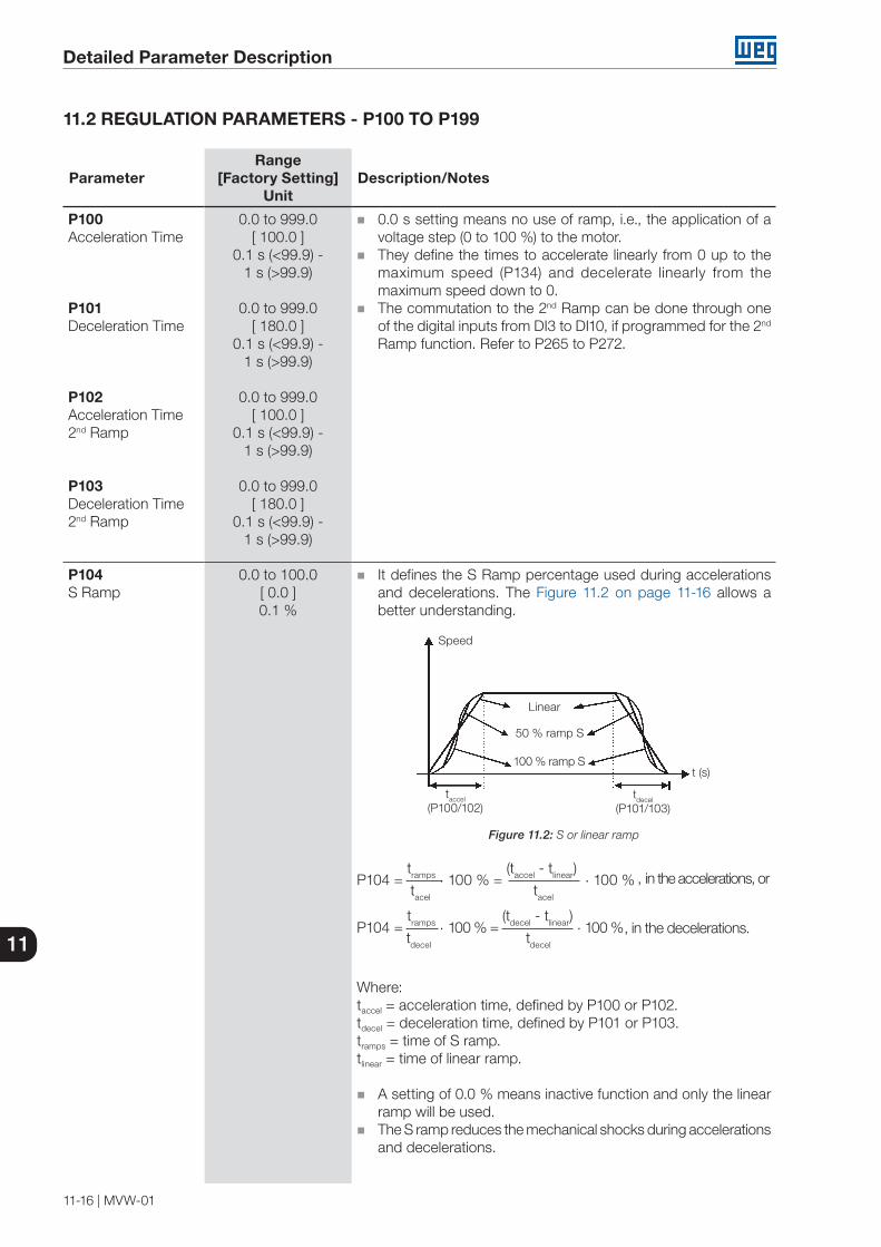
Detailed Parameter Description
11-16 | MVW-01
11
11.2 REGULATION PARAMETERS - P100 TO P199
ParameterRange
[Factory Setting]Unit
Description/Notes
P100Acceleration Time
P101Deceleration Time
P102Acceleration Time2nd Ramp
P103Deceleration Time2nd Ramp
0.0 to 999.0[ 100.0 ]
0.1 s (<99.9) - 1 s (>99.9)
0.0 to 999.0[ 180.0 ]
0.1 s (<99.9) -1 s (>99.9)
0.0 to 999.0[ 100.0 ]
0.1 s (<99.9) -1 s (>99.9)
0.0 to 999.0[ 180.0 ]
0.1 s (<99.9) -1 s (>99.9)
0.0 s setting means no use of ramp, i.e., the application of a voltage step (0 to 100 %) to the motor.
They define the times to accelerate linearly from 0 up to the maximum speed (P134) and decelerate linearly from the maximum speed down to 0.
The commutation to the 2nd Ramp can be done through one of the digital inputs from DI3 to DI10, if programmed for the 2nd Ramp function. Refer to P265 to P272.
P104S Ramp
0.0 to 100.0[ 0.0 ]0.1 %
It defines the S Ramp percentage used during accelerations and decelerations. The Figure 11.2 on page 11-16 allows a better understanding.
Speed
Linear
t (s)
taccel
(P100/102)tdecel
(P101/103)
50 % ramp S
100 % ramp S
Figure 11.2: S or linear ramp
P104 = tramps . 100 % =
(taccel - tlinear) . 100 % tacel tacel
, in the accelerations, or
P104 = tramps . 100 % =
(tdecel - tlinear) . 100 % tdecel tdecel
, in the decelerations.
Where:taccel = acceleration time, defined by P100 or P102.tdecel = deceleration time, defined by P101 or P103.tramps = time of S ramp.tlinear = time of linear ramp.
A setting of 0.0 % means inactive function and only the linear ramp will be used.
The S ramp reduces the mechanical shocks during accelerations and decelerations.
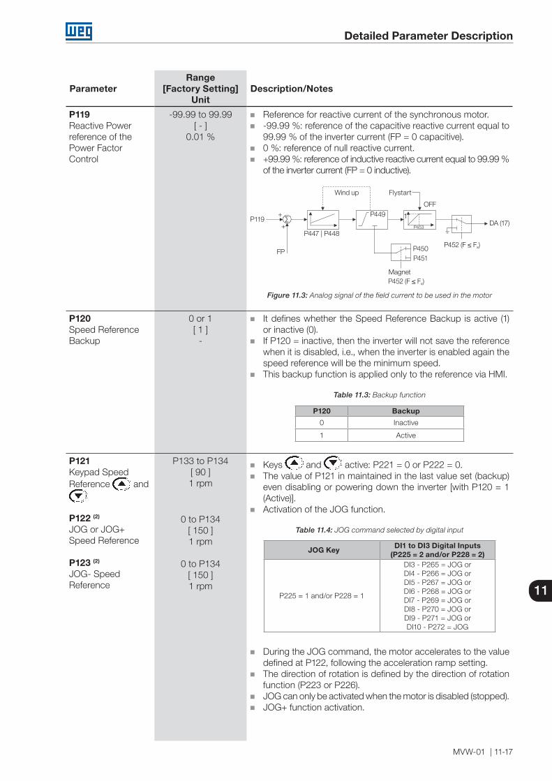
Detailed Parameter Description
MVW-01 | 11-17
11
ParameterRange
[Factory Setting]Unit
Description/Notes
P119Reactive Power reference of the Power Factor Control
-99.99 to 99.99[ - ]
0.01 %
Reference for reactive current of the synchronous motor. -99.99 %: reference of the capacitive reactive current equal to
99.99 % of the inverter current (FP = 0 capacitive). 0 %: reference of null reactive current. +99.99 %: reference of inductive reactive current equal to 99.99 %
of the inverter current (FP = 0 inductive).
P449
P453
P450
Magnet
FlystartWind up
P452 (F ≤ Fx)
P452 (F ≤ Fx)
P451FP
∑ 1+
+
OFF
DA (17)P119
P447 | P448
Figure 11.3: Analog signal of the field current to be used in the motor
P120Speed Reference Backup
0 or 1[ 1 ]
-
It defines whether the Speed Reference Backup is active (1) or inactive (0).
If P120 = inactive, then the inverter will not save the reference when it is disabled, i.e., when the inverter is enabled again the speed reference will be the minimum speed.
This backup function is applied only to the reference via HMI.
Table 11.3: Backup function
P120 Backup
0 Inactive
1 Active
P121Keypad Speed Reference and
P122 (2)
JOG or JOG+Speed Reference
P123 (2)
JOG- SpeedReference
P133 to P134[ 90 ]1 rpm
0 to P134[ 150 ]1 rpm
0 to P134[ 150 ]1 rpm
Keys and active: P221 = 0 or P222 = 0. The value of P121 in maintained in the last value set (backup)
even disabling or powering down the inverter [with P120 = 1 (Active)].
Activation of the JOG function.
Table 11.4: JOG command selected by digital input
JOG Key DI1 to DI3 Digital Inputs(P225 = 2 and/or P228 = 2)
P225 = 1 and/or P228 = 1
DI3 - P265 = JOG orDI4 - P266 = JOG orDI5 - P267 = JOG orDI6 - P268 = JOG orDI7 - P269 = JOG orDI8 - P270 = JOG orDI9 - P271 = JOG orDI10 - P272 = JOG
During the JOG command, the motor accelerates to the value defined at P122, following the acceleration ramp setting.
The direction of rotation is defined by the direction of rotation function (P223 or P226).
JOG can only be activated when the motor is disabled (stopped). JOG+ function activation.

Detailed Parameter Description
11-18 | MVW-01
11
ParameterRange
[Factory Setting]Unit
Description/Notes
Table 11.5: JOG+ command selection
Digital Inputs Parameters
DI3 to DI10 P265 to P272 = JOG+
JOG- function activation:
Table 11.6: JOG- command selection
Digital Inputs Parameters
DI3 to DI10 P265 to P272 = JOG-
During the JOG+ or JOG- commands the values of P122 or P123 are, respectively, added to or subtracted from the speed reference, to generate the total reference - refer to the Figure 11.26 on page 11-48.
P124 (2)
MultispeedReference 1
P125 (2)
MultispeedReference 2
P126 (2)
MultispeedReference 3
P127 (2)
MultispeedReference 4
P128 (2)
MultispeedReference 5
P129 (2)
MultispeedReference 6
P130 (2)
MultispeedReference 7
P131 (2)
MultispeedReference 8
P133 to P134[ 90 ]1 rpm
P133 to P134[ 300 ]1 rpm
P133 to P134[ 600 ]1 rpm
P133 to P134[ 900 ]1 rpm
P133 to P134[ 1200 ]1 rpm
P133 to P134[ 1500 ]1 rpm
P133 to P134[ 1800 ]1 rpm
P133 to P134[ 1650 ]1 rpm
The parameters from P124 to P131 will only be shown when P221 = 8 and/or P222 = 8 (Multispeed).
Multispeed is used when up to 8 fixed pre-programmed speeds are required.
When just 2 or 4 speeds are required, any combination of inputs between DI4, DI5 and DI6 can be used. Verify the speed reference parameters according to the used DIs.
The inputs programmed for other functions must be considered as 0 V in the Table 11.8 on page 11-18.
The stability of the fixed pre-programmed references and their immunity against electric noises (isolated digital inputs) are advantages of the Multispeed function.
The Multispeed function is active only when P221 or P222 = Multispeed.
It allows control of the output speed by associating the values defined in the parameters P124 to P131 to the logic combination of the digital inputs.
Table 11.7: Multispeed function selected by digital input
Enabled Digital Input Programming4 P266 = 75 P267 = 76 P268 = 7
Table 11.8: Multispeed references
8 Speeds
SpeedReference
4 Speeds2 Speeds
DI6 DI5 DI40 0 0 P1240 0 1 P1250 1 0 P1260 1 1 P1271 0 0 P1281 0 1 P1291 1 0 P1301 1 1 P131
Detailed Parameter Description
MVW-01 | 11-19
11
ParameterRange
[Factory Setting]Unit
Description/Notes
P132Maximum level of Overspeed
Thisparameter isonly visible in thedisplay(s) when P202 = 3 or 4 (Vector Control)
0 to 100[ 10 ]1 %
When the actual speed exceeds the value of P134 + P132 for over 20 ms, the MVW-01 will disable the pulses of the PWM and it will indicate fault F112.
The setting of P132 is a percentage valued of P134. When setting P132 = 100 % the function will be disabled.
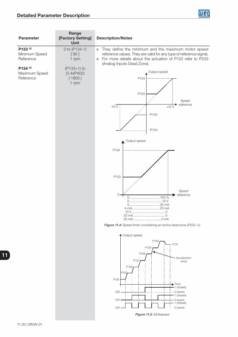
Detailed Parameter Description
11-20 | MVW-01
11
ParameterRange
[Factory Setting]Unit
Description/Notes
P133 (2)
Minimum SpeedReference
P134 (2)
Maximum SpeedReference
0 to (P134-1)[ 90 ]1 rpm
(P133+1) to (3.4xP402)
[ 1800 ]1 rpm
They define the minimum and the maximum motor speed reference values. They are valid for any type of reference signal.
For more details about the actuation of P133 refer to P233 (Analog Inputs Dead Zone).
P134
P133
+10 V
-P133
-P134
-10 V
Speed reference
Output speed
P134
P133
Speed reference
Output speed
0 .................................. 100 % 0 .....................................10 V 0 .................................. 20 mA 4 mA............................... 20 mA 10 V ..................................... 0 20 mA.................................... 0 20 mA................................4 mA
0
Figure 11.4: Speed limits considering an active dead zone (P233 =1)
Acceleration ramp
Time1 (closed)
DI6
DI5
DI4
0 (open)1 (closed)
0 (open)1 (closed)
0 (open)
P124
P125
P126
P127
P128
P129
P130P131
Output speed
Figure 11.5: Multispeed
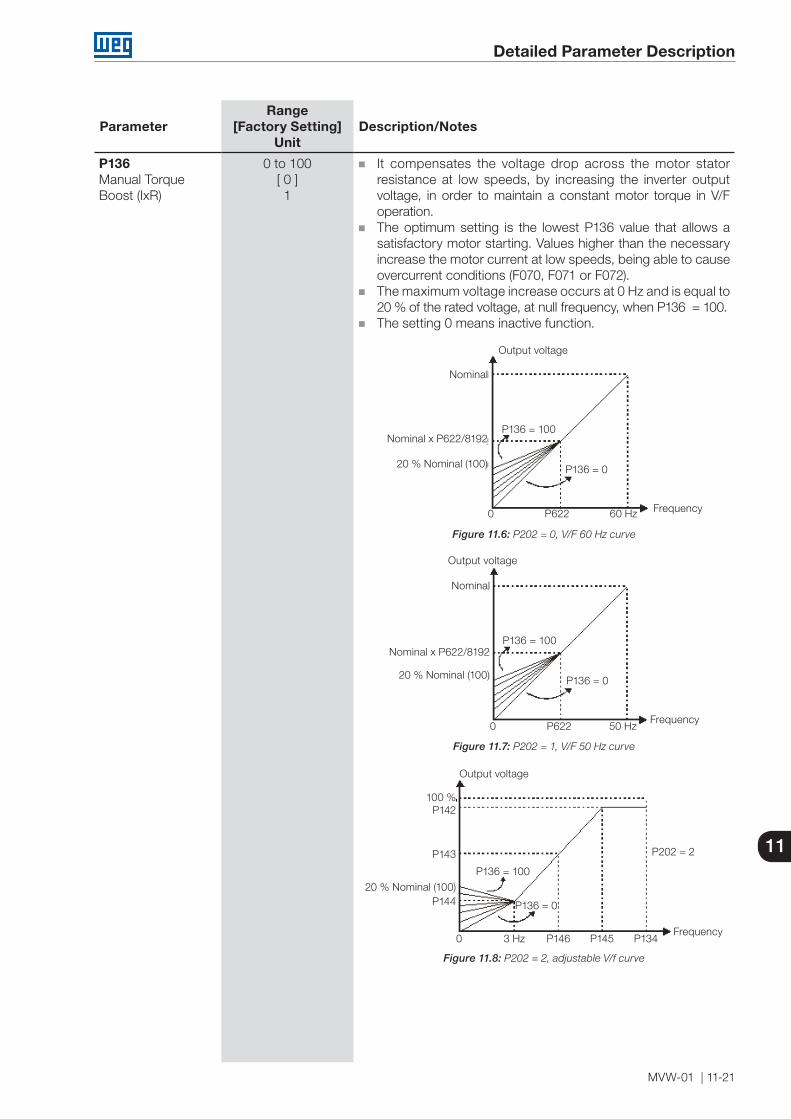
Detailed Parameter Description
MVW-01 | 11-21
11
ParameterRange
[Factory Setting]Unit
Description/Notes
P136Manual TorqueBoost (IxR)
0 to 100[ 0 ]1
It compensates the voltage drop across the motor stator resistance at low speeds, by increasing the inverter output voltage, in order to maintain a constant motor torque in V/F operation.
The optimum setting is the lowest P136 value that allows a satisfactory motor starting. Values higher than the necessary increase the motor current at low speeds, being able to cause overcurrent conditions (F070, F071 or F072).
The maximum voltage increase occurs at 0 Hz and is equal to 20 % of the rated voltage, at null frequency, when P136 = 100.
The setting 0 means inactive function.
Frequency
Nominal x P622/8192
20 % Nominal (100)
Output voltage
0 P622 60 Hz
Nominal
P136 = 100
P136 = 0
Figure 11.6: P202 = 0, V/F 60 Hz curve
Frequency
Nominal x P622/8192
20 % Nominal (100)
Output voltage
0 P622 50 Hz
Nominal
P136 = 100
P136 = 0
Figure 11.7: P202 = 1, V/F 50 Hz curve
Frequency
P143
P146 P145 P1343 Hz0
P14420 % Nominal (100)
Output voltage
100 % P142
P136 = 100
P136 = 0
P202 = 2
Figure 11.8: P202 = 2, adjustable V/f curve
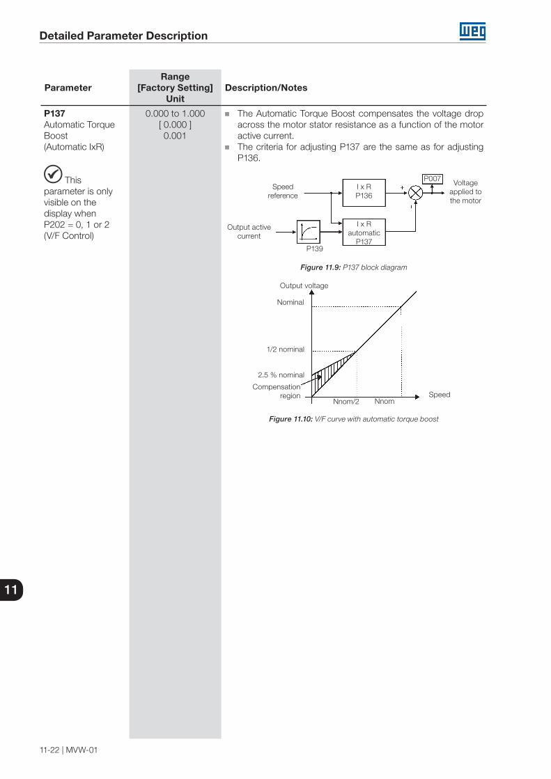
Detailed Parameter Description
11-22 | MVW-01
11
ParameterRange
[Factory Setting]Unit
Description/Notes
P137Automatic TorqueBoost(Automatic IxR)
Thisparameter is onlyvisible on thedisplay whenP202 = 0, 1 or 2(V/F Control)
0.000 to 1.000[ 0.000 ]0.001
The Automatic Torque Boost compensates the voltage drop across the motor stator resistance as a function of the motor active current.
The criteria for adjusting P137 are the same as for adjusting P136.
P139
P007Speed
reference
Voltageapplied tothe motor
I x RP136
I x Rautomatic
P137
Output activecurrent
Figure 11.9: P137 block diagram
Speed
1/2 nominal
2.5 % nominal
Compensationregion
Nnom/2 Nnom
Output voltage
Nominal
Figure 11.10: V/F curve with automatic torque boost
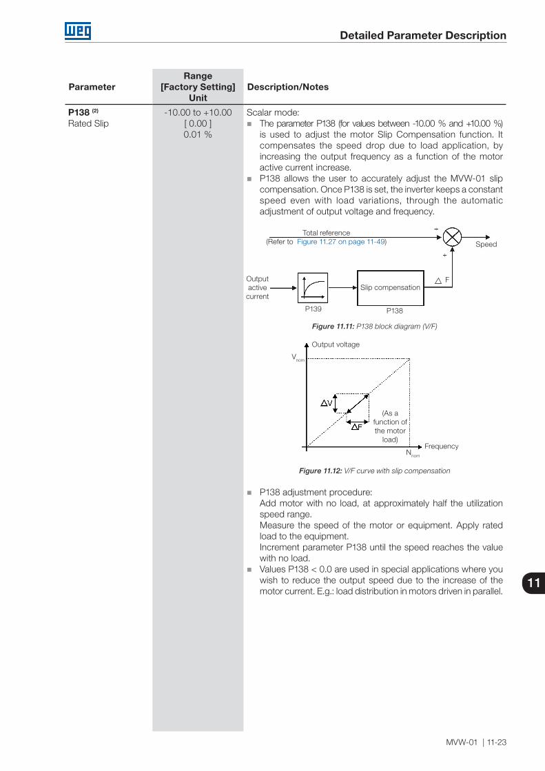
Detailed Parameter Description
MVW-01 | 11-23
11
ParameterRange
[Factory Setting]Unit
Description/Notes
P138 (2)
Rated Slip-10.00 to +10.00
[ 0.00 ]0.01 %
Scalar mode: The parameter P138 (for values between -10.00 % and +10.00 %)
is used to adjust the motor Slip Compensation function. It compensates the speed drop due to load application, by increasing the output frequency as a function of the motor active current increase.
P138 allows the user to accurately adjust the MVW-01 slip compensation. Once P138 is set, the inverter keeps a constant speed even with load variations, through the automatic adjustment of output voltage and frequency.
Total reference (Refer to Figure 11.27 on page 11-49) Speed
Outputactive
current
P139 P138
Slip compensationF
Figure 11.11: P138 block diagram (V/F)
Output voltage
Frequency
(As afunction ofthe motor
load)
Vnom
Nnom
Figure 11.12: V/F curve with slip compensation
P138 adjustment procedure:Add motor with no load, at approximately half the utilization speed range.Measure the speed of the motor or equipment. Apply rated load to the equipment.Increment parameter P138 until the speed reaches the value with no load.
Values P138 < 0.0 are used in special applications where you wish to reduce the output speed due to the increase of the motor current. E.g.: load distribution in motors driven in parallel.
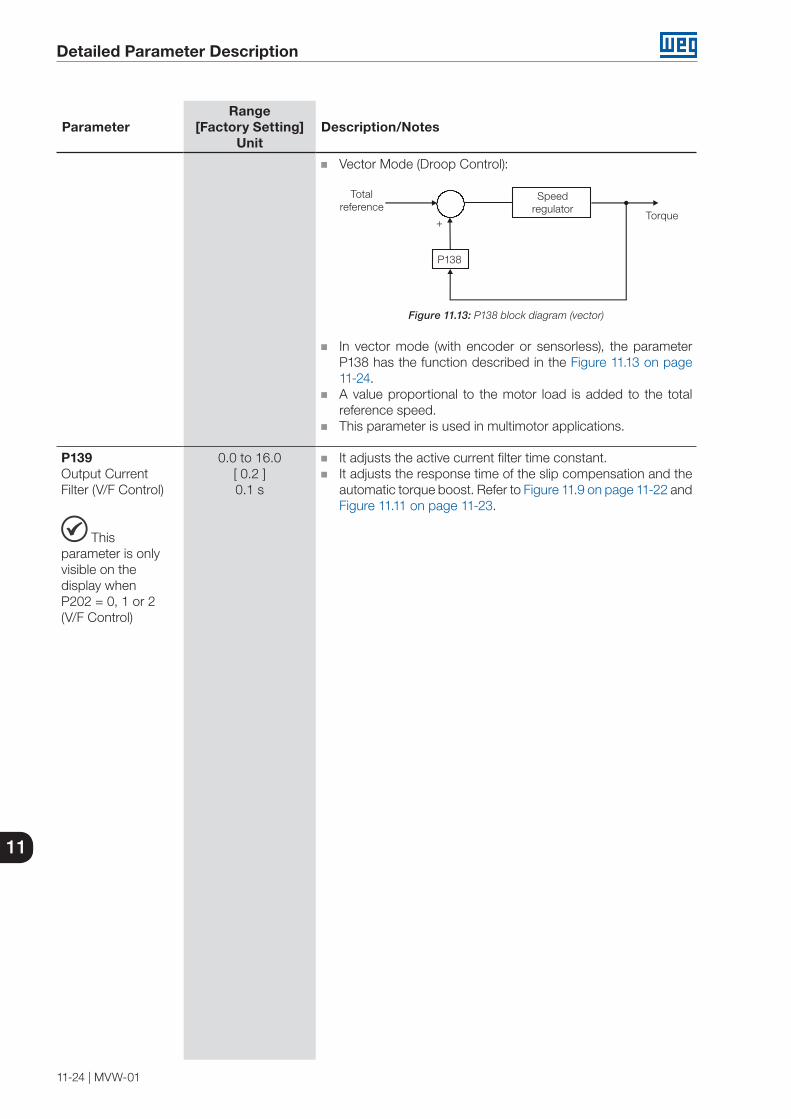
Detailed Parameter Description
11-24 | MVW-01
11
ParameterRange
[Factory Setting]Unit
Description/Notes
Vector Mode (Droop Control):
Speedregulator
P138
+
Totalreference
Torque
Figure 11.13: P138 block diagram (vector)
In vector mode (with encoder or sensorless), the parameter P138 has the function described in the Figure 11.13 on page 11-24.
A value proportional to the motor load is added to the total reference speed.
This parameter is used in multimotor applications.
P139Output CurrentFilter (V/F Control)
Thisparameter is onlyvisible on thedisplay whenP202 = 0, 1 or 2(V/F Control)
0.0 to 16.0[ 0.2 ]0.1 s
It adjusts the active current filter time constant. It adjusts the response time of the slip compensation and the
automatic torque boost. Refer to Figure 11.9 on page 11-22 and Figure 11.11 on page 11-23.
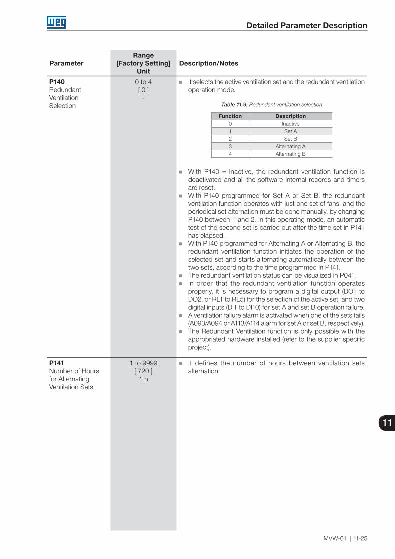
Detailed Parameter Description
MVW-01 | 11-25
11
ParameterRange
[Factory Setting]Unit
Description/Notes
P140RedundantVentilationSelection
0 to 4[ 0 ]
-
It selects the active ventilation set and the redundant ventilation operation mode.
Table 11.9: Redundant ventilation selection
Function Description0 Inactive1 Set A2 Set B3 Alternating A4 Alternating B
With P140 = Inactive, the redundant ventilation function is deactivated and all the software internal records and timers are reset.
With P140 programmed for Set A or Set B, the redundant ventilation function operates with just one set of fans, and the periodical set alternation must be done manually, by changing P140 between 1 and 2. In this operating mode, an automatic test of the second set is carried out after the time set in P141 has elapsed.
With P140 programmed for Alternating A or Alternating B, the redundant ventilation function initiates the operation of the selected set and starts alternating automatically between the two sets, according to the time programmed in P141.
The redundant ventilation status can be visualized in P041. In order that the redundant ventilation function operates
properly, it is necessary to program a digital output (DO1 to DO2, or RL1 to RL5) for the selection of the active set, and two digital inputs (DI1 to DI10) for set A and set B operation failure.
A ventilation failure alarm is activated when one of the sets fails (A093/A094 or A113/A114 alarm for set A or set B, respectively).
The Redundant Ventilation function is only possible with the appropriated hardware installed (refer to the supplier specific project).
P141Number of Hoursfor AlternatingVentilation Sets
1 to 9999[ 720 ]
1 h
It defines the number of hours between ventilation sets alternation.
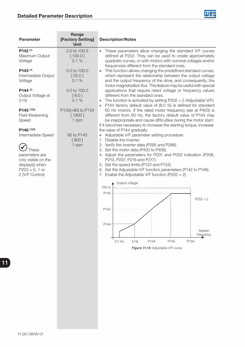
Detailed Parameter Description
11-26 | MVW-01
11
ParameterRange
[Factory Setting]Unit
Description/Notes
P142 (1)
Maximum OutputVoltage
P143 (1)
Intermediate OutputVoltage
P144 (1)
Output Voltage at 3 Hz
P145 (1)(2)
Field WeakeningSpeed
P146 (1)(2)
Intermediate Speed
Theseparameters areonly visible on thedisplay(s) when P202 = 0, 1 or2 (V/F Control)
0.0 to 100.0[ 100.0 ]0.1 %
0.0 to 100.0[ 50.0 ]0.1 %
0.0 to 100.0[ 8.0 ]0.1 %
P133(>90) to P134[ 1800 ]1 rpm
90 to P145[ 900 ]1 rpm
These parameters allow changing the standard V/F curves defined at P202. They can be used to create approximately quadratic curves, or with motors with nominal voltages and/or frequencies different from the standard ones.
This function allows changing the predefined standard curves, which represent the relationship between the output voltage and the output frequency of the drive, and consequently, the motor magnetization flux. This feature may be useful with special applications that require rated voltage or frequency values different from the standard ones.
The function is activated by setting P202 = 2 (Adjustable V/F). P144 factory default value of (8.0 %) is defined for standard
60 Hz motors. If the rated motor frequency (set at P403) is different from 60 Hz, the factory default value of P144 may be inappropriate and cause difficulties during the motor start.
If it becomes necessary to increase the starting torque, increasethe value of P144 gradually.
Adjustable V/F parameter setting procedure:1. Disable the inverter.2. Verify the inverter data (P295 and P296).3. Set the motor data (P400 to P406).4. Adjust the parameters for P001 and P002 indication (P208,
P210, P207, P216 and P217).5. Set the speed limits (P133 and P134).6. Set the Adjustable V/F function parameters (P142 to P146).7. Enable the Adjustable V/F function (P202 = 2).
100 %
P142
P143
P144
0.1 Hz 3 Hz P146 P145
P202 = 2
Output voltage
Speed/frequency
P134
Figure 11.14: Adjustable V/F curve

Detailed Parameter Description
MVW-01 | 11-27
11
ParameterRange
[Factory Setting]Unit
Description/Notes
P150 (1)
DC Link VoltageRegulation Mode
Thisparameter isonly visible in thedisplay(s) whenP202 = 3 or 4(Vector Control)
0 to 2[ 2 ]
-
Table 11.10: DC Link voltage regulation mode
P150 Action
0 = withoutlosses
(Normal)
Deceleration ramp control equal to the scalar mode. Setting in P151.
1 = withoutlosses
(Automatic)
Automatic deceleration ramp control. The Optimal Braking is inactive. The deceleration ram is automatically set to keep the DC link below the level set in P151. This procedure avoids F022 – overvoltage on the DC link. I can also be used with eccentric loads.
2 = withlosses
(OptimalBraking)
The Optimal Breaking is active as described in P151 for vector control. That gives the smallest deceleration time possible without using dynamic or regenerative braking. Maximum rotor flux set in in P179.
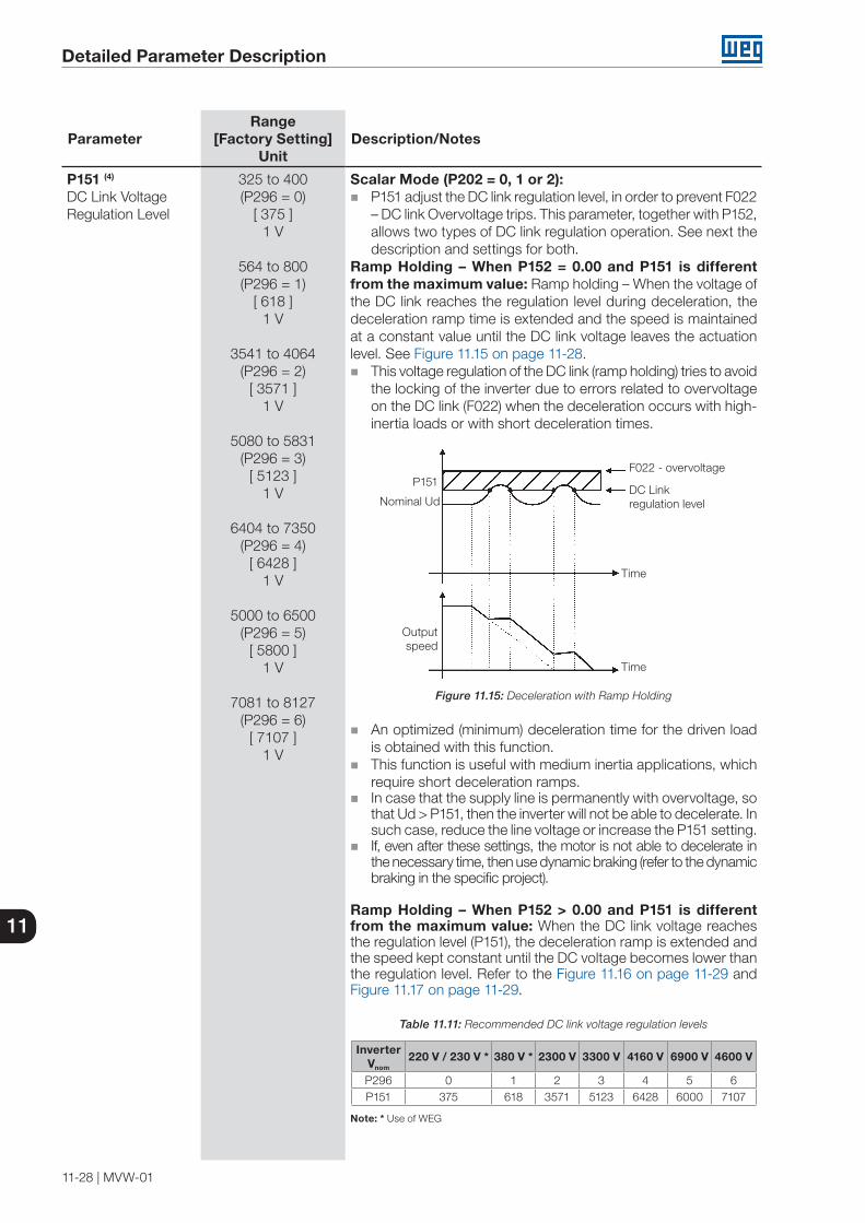
Detailed Parameter Description
11-28 | MVW-01
11
ParameterRange
[Factory Setting]Unit
Description/Notes
P151 (4)
DC Link VoltageRegulation Level
325 to 400 (P296 = 0)
[ 375 ]1 V
564 to 800 (P296 = 1)
[ 618 ]1 V
3541 to 4064 (P296 = 2)
[ 3571 ]1 V
5080 to 5831 (P296 = 3)
[ 5123 ]1 V
6404 to 7350 (P296 = 4)
[ 6428 ]1 V
5000 to 6500 (P296 = 5)
[ 5800 ]1 V
7081 to 8127 (P296 = 6)
[ 7107 ]1 V
Scalar Mode (P202 = 0, 1 or 2): P151 adjust the DC link regulation level, in order to prevent F022
– DC link Overvoltage trips. This parameter, together with P152, allows two types of DC link regulation operation. See next the description and settings for both.
Ramp Holding – When P152 = 0.00 and P151 is different from the maximum value: Ramp holding – When the voltage of the DC link reaches the regulation level during deceleration, the deceleration ramp time is extended and the speed is maintained at a constant value until the DC link voltage leaves the actuation level. See Figure 11.15 on page 11-28.
This voltage regulation of the DC link (ramp holding) tries to avoid the locking of the inverter due to errors related to overvoltage on the DC link (F022) when the deceleration occurs with high-inertia loads or with short deceleration times.
F022 - overvoltage
DC Linkregulation level
Time
Time
Outputspeed
Nominal Ud
P151
Figure 11.15: Deceleration with Ramp Holding
An optimized (minimum) deceleration time for the driven load is obtained with this function.
This function is useful with medium inertia applications, which require short deceleration ramps.
In case that the supply line is permanently with overvoltage, so that Ud > P151, then the inverter will not be able to decelerate. In such case, reduce the line voltage or increase the P151 setting.
If, even after these settings, the motor is not able to decelerate in the necessary time, then use dynamic braking (refer to the dynamic braking in the specific project).
Ramp Holding – When P152 > 0.00 and P151 is different from the maximum value: When the DC link voltage reaches the regulation level (P151), the deceleration ramp is extended andthe speed kept constant until the DC voltage becomes lower thanthe regulation level. Refer to the Figure 11.16 on page 11-29 and Figure 11.17 on page 11-29.
Table 11.11: Recommended DC link voltage regulation levels
InverterVnom
220 V / 230 V * 380 V * 2300 V 3300 V 4160 V 6900 V 4600 V
P296 0 1 2 3 4 5 6P151 375 618 3571 5123 6428 6000 7107
Note: * Use of WEG
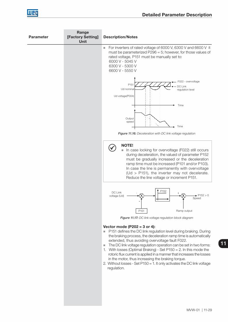
Detailed Parameter Description
MVW-01 | 11-29
11
ParameterRange
[Factory Setting]Unit
Description/Notes
For inverters of rated voltage of 6000 V, 6300 V and 6600 V it must be parameterized P296 = 5; however, for those values of rated voltage, P151 must be manually set to:6000 V - 5045 V6300 V - 5300 V6600 V - 5550 V
F022 - overvoltage
Ud voltage(P004)
Time
Time
Outputspeed
Ud nominal
P151DC Linkregulation level
Figure 11.16: Deceleration with DC link voltage regulation
NOTE! In case locking for overvoltage (F022) still occurs
during deceleration, the valued of parameter P152 must be gradually increased or the deceleration ramp time must be increased (P101 and/or P103). In case the line is permanently with overvoltage (Ud > P151), the inverter may not decelerate. Reduce the line voltage or increment P151.
DC Linkvoltage (Ud)
P152
SpeedP152 > 0
Ramp outputP151
Figure 11.17: DC link voltage regulation block diagram
Vector mode (P202 = 3 or 4): P151 defines the DC link regulation level during braking. During
the braking process, the deceleration ramp time is automatically extended, thus avoiding overvoltage fault F022.
The DC link voltage regulation operation can be set in two forms:1. With losses (Optimal Braking) - Set P150 = 2. In this mode the rotoric flux current is applied in a manner that increases the losses in the motor, thus increasing the braking torque.2. Without losses - Set P150 = 1. It only activates the DC link voltage regulation.
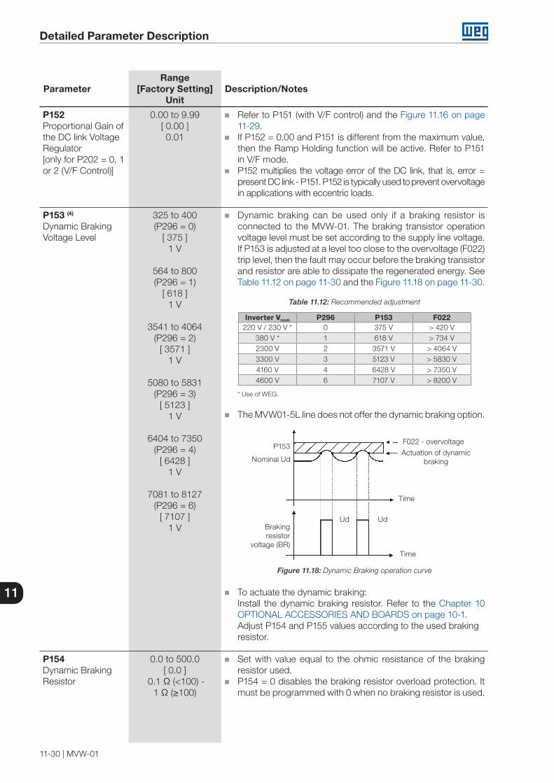
Detailed Parameter Description
11-30 | MVW-01
11
ParameterRange
[Factory Setting]Unit
Description/Notes
P152Proportional Gain of the DC link Voltage Regulator[only for P202 = 0, 1 or 2 (V/F Control)]
0.00 to 9.99[ 0.00 ]0.01
Refer to P151 (with V/F control) and the Figure 11.16 on page 11-29.
If P152 = 0.00 and P151 is different from the maximum value, then the Ramp Holding function will be active. Refer to P151 in V/F mode.
P152 multiplies the voltage error of the DC link, that is, error = present DC link - P151. P152 is typically used to prevent overvoltage in applications with eccentric loads.
P153 (4)
Dynamic BrakingVoltage Level
325 to 400 (P296 = 0)
[ 375 ]1 V
564 to 800 (P296 = 1)
[ 618 ]1 V
3541 to 4064 (P296 = 2)
[ 3571 ]1 V
5080 to 5831 (P296 = 3)
[ 5123 ]1 V
6404 to 7350(P296 = 4)
[ 6428 ]1 V
7081 to 8127(P296 = 6)
[ 7107 ]1 V
Dynamic braking can be used only if a braking resistor is connected to the MVW-01. The braking transistor operation voltage level must be set according to the supply line voltage. If P153 is adjusted at a level too close to the overvoltage (F022) trip level, then the fault may occur before the braking transistor and resistor are able to dissipate the regenerated energy. See Table 11.12 on page 11-30 and the Figure 11.18 on page 11-30.
Table 11.12: Recommended adjustment
Inverter Vnom P296 P153 F022220 V / 230 V * 0 375 V > 420 V
380 V * 1 618 V > 734 V2300 V 2 3571 V > 4064 V3300 V 3 5123 V > 5830 V4160 V 4 6428 V > 7350 V4600 V 6 7107 V > 8200 V
* Use of WEG.
The MVW01-5L line does not offer the dynamic braking option.
F022 - overvoltage
Actuation of dynamic braking
Time
Time
Brakingresistor
voltage (BR)
UdUd
P153
Nominal Ud
Figure 11.18: Dynamic Braking operation curve
To actuate the dynamic braking:Install the dynamic braking resistor. Refer to the Chapter 10 OPTIONAL ACCESSORIES AND BOARDS on page 10-1.Adjust P154 and P155 values according to the used brakingresistor.
P154Dynamic BrakingResistor
0.0 to 500.0[ 0.0 ]
0.1 Ω (<100) - 1 Ω (≥100)
Set with value equal to the ohmic resistance of the braking resistor used.
P154 = 0 disables the braking resistor overload protection. It must be programmed with 0 when no braking resistor is used.
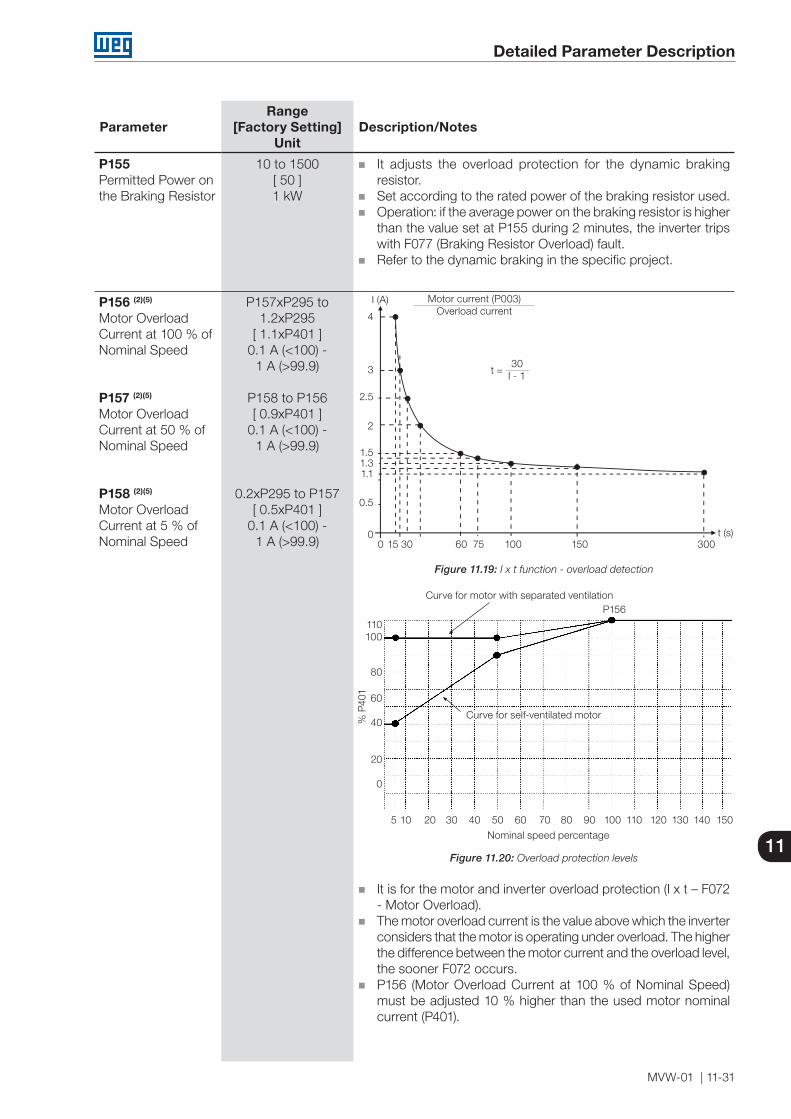
Detailed Parameter Description
MVW-01 | 11-31
11
ParameterRange
[Factory Setting]Unit
Description/Notes
P155Permitted Power on the Braking Resistor
10 to 1500[ 50 ]1 kW
It adjusts the overload protection for the dynamic braking resistor.
Set according to the rated power of the braking resistor used. Operation: if the average power on the braking resistor is higher
than the value set at P155 during 2 minutes, the inverter trips with F077 (Braking Resistor Overload) fault.
Refer to the dynamic braking in the specific project.
P156 (2)(5)
Motor OverloadCurrent at 100 % ofNominal Speed
P157 (2)(5)
Motor OverloadCurrent at 50 % ofNominal Speed
P158 (2)(5)
Motor OverloadCurrent at 5 % ofNominal Speed
P157xP295 to 1.2xP295
[ 1.1xP401 ]0.1 A (<100) -
1 A (>99.9)
P158 to P156[ 0.9xP401 ]
0.1 A (<100) -1 A (>99.9)
0.2xP295 to P157[ 0.5xP401 ]
0.1 A (<100) -1 A (>99.9)
Motor current (P003)Overload current
t = 30
I - 1
t (s)
I (A)
0 15 30 60 75 100 150 300
4
3
2.5
2
1.51.31.1
0.5
0
Figure 11.19: I x t function - overload detection
Nominal speed percentage
% P
401
P156
P157
5 10 20 30 40 50 60 70 80 90 100 110 120 130 140 150
110100
80
60
40
20
0
P158
Curve for motor with separated ventilation
Curve for self-ventilated motor
Figure 11.20: Overload protection levels
It is for the motor and inverter overload protection (I x t – F072 - Motor Overload).
The motor overload current is the value above which the inverter considers that the motor is operating under overload. The higher the difference between the motor current and the overload level, the sooner F072 occurs.
P156 (Motor Overload Current at 100 % of Nominal Speed) must be adjusted 10 % higher than the used motor nominal current (P401).
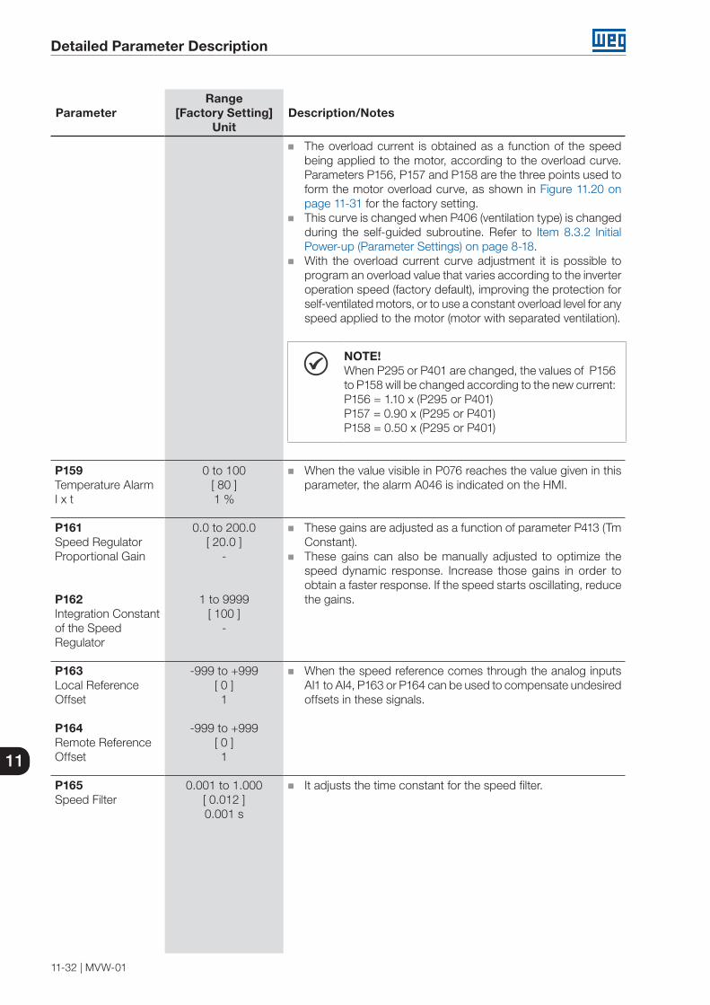
Detailed Parameter Description
11-32 | MVW-01
11
ParameterRange
[Factory Setting]Unit
Description/Notes
The overload current is obtained as a function of the speed being applied to the motor, according to the overload curve. Parameters P156, P157 and P158 are the three points used to form the motor overload curve, as shown in Figure 11.20 on page 11-31 for the factory setting.
This curve is changed when P406 (ventilation type) is changed during the self-guided subroutine. Refer to Item 8.3.2 Initial Power-up (Parameter Settings) on page 8-18.
With the overload current curve adjustment it is possible to program an overload value that varies according to the inverter operation speed (factory default), improving the protection for self-ventilated motors, or to use a constant overload level for any speed applied to the motor (motor with separated ventilation).
NOTE!When P295 or P401 are changed, the values of P156 to P158 will be changed according to the new current: P156 = 1.10 x (P295 or P401)P157 = 0.90 x (P295 or P401)P158 = 0.50 x (P295 or P401)
P159Temperature Alarm I x t
0 to 100[ 80 ]1 %
When the value visible in P076 reaches the value given in this parameter, the alarm A046 is indicated on the HMI.
P161Speed RegulatorProportional Gain
P162Integration Constant of the Speed Regulator
0.0 to 200.0[ 20.0 ]
-
1 to 9999[ 100 ]
-
These gains are adjusted as a function of parameter P413 (Tm Constant).
These gains can also be manually adjusted to optimize the speed dynamic response. Increase those gains in order to obtain a faster response. If the speed starts oscillating, reduce the gains.
P163Local ReferenceOffset
P164 Remote ReferenceOffset
-999 to +999[ 0 ]1
-999 to +999[ 0 ]1
When the speed reference comes through the analog inputs AI1 to AI4, P163 or P164 can be used to compensate undesired offsets in these signals.
P165 Speed Filter
0.001 to 1.000[ 0.012 ]0.001 s
It adjusts the time constant for the speed filter.
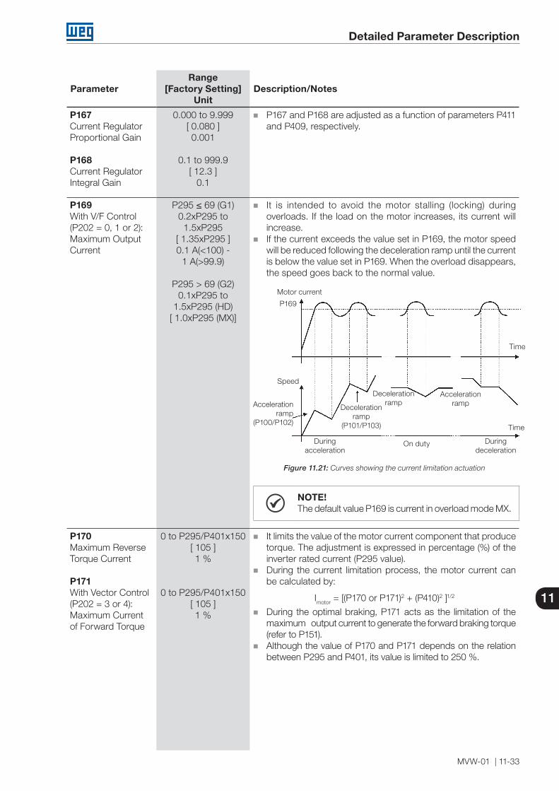
Detailed Parameter Description
MVW-01 | 11-33
11
ParameterRange
[Factory Setting]Unit
Description/Notes
P167Current RegulatorProportional Gain
P168Current RegulatorIntegral Gain
0.000 to 9.999[ 0.080 ]0.001
0.1 to 999.9[ 12.3 ]
0.1
P167 and P168 are adjusted as a function of parameters P411 and P409, respectively.
P169With V/F Control (P202 = 0, 1 or 2):Maximum Output Current
P295 ≤ 69 (G1) 0.2xP295 to
1.5xP295 [ 1.35xP295 ] 0.1 A(<100) -
1 A(>99.9)
P295 > 69 (G2) 0.1xP295 to
1.5xP295 (HD) [ 1.0xP295 (MX)]
It is intended to avoid the motor stalling (locking) during overloads. If the load on the motor increases, its current will increase.
If the current exceeds the value set in P169, the motor speed will be reduced following the deceleration ramp until the current is below the value set in P169. When the overload disappears, the speed goes back to the normal value.
Motor current
P169
Time
On duty
Decelerationramp
(P101/P103)
Decelerationramp
Accelerationramp
Duringdeceleration
Duringacceleration
Accelerationramp
(P100/P102)
Speed
Time
Figure 11.21: Curves showing the current limitation actuation
NOTE!The default value P169 is current in overload mode MX.
P170Maximum ReverseTorque Current
P171With Vector Control (P202 = 3 or 4):Maximum Current of Forward Torque
0 to P295/P401x150[ 105 ]1 %
0 to P295/P401x150[ 105 ]1 %
It limits the value of the motor current component that produce torque. The adjustment is expressed in percentage (%) of the inverter rated current (P295 value).
During the current limitation process, the motor current can be calculated by:
Imotor = [(P170 or P171)2 + (P410)2 ]1/2
During the optimal braking, P171 acts as the limitation of the maximum output current to generate the forward braking torque (refer to P151).
Although the value of P170 and P171 depends on the relation between P295 and P401, its value is limited to 250 %.

Detailed Parameter Description
11-34 | MVW-01
11
ParameterRange
[Factory Setting]Unit
Description/Notes
P175 (1)
Flux RegulatorProportional Gain
P176 (3)
Integration Constant of the Flux Regulator
0.0 to 999.9[50.0]0.1
1 to 9999[ 900 ]
-
These gains are adjusted as a function of the parameter P412.
P177Minimum Flux
P178Nominal Flux
P179Maximum Flux
0 to 120[ 0 ]1 %
0 to 120[ 100 ]1 %
0 to 200[ 120 ]1 %
Motor flux conditions.
P180Starting Point of the Field Weakening
This parameter is only visible with P202 > 2.
0 to 120[ 85 ]1 %
It expresses the % of the modulation index from which the motor field weakening occurs.
P181MagnetizationMode
0 or 1[ 0 ]
-
Table 11.13: Magnetization mode
P181 Action
0 = General EnableIt applies magnetization current after
General Enable ON
1 = Start/StopIt applies magnetization current after
Start/Stop ON
Detailed Parameter Description
MVW-01 | 11-35
11
ParameterRange
[Factory Setting]Unit
Description/Notes
P182Flux ReferenceRegulatorProportional Gain
This parameter is only visible with P202 > 2.
P183Flux ReferenceRegulator IntegralGain
This parameter is only visible with P202 > 2.
0.00 to 99.99[ 0.20 ]
0.1
1 to 9999[ 25 ]
-
PI gains of the flux regulator.
11.3 CONFIGURATION PARAMETERS - P200 TO P399
ParameterRange
[Factory Setting]Unit
Description/Notes
P200Password
0 or 1[ 1 ]
-
Table 11.14: Password status
P200 Result
0 (Inactive)Disables the password and allows changingparameters content regardless of P000 setting.
1 (Active)Enables the password that allows changingparameter contents only when P000 is equal tothat password.
The factory default value for the password is P000 = 5. Refer to P000 in order to change the password.
P201Language Selection
0 to 3[ To be defined by
the user ]-
Table 11.15: Language selection
P201 Language0 Portuguese1 English2 Español3 Deutsch

Detailed Parameter Description
11-36 | MVW-01
11
ParameterRange
[Factory Setting]Unit
Description/Notes
P202 (1)(2)
Control Type0 to 4[ 0 ]
-
Table 11.16: Control type selection
P202 Control Type0 V/F 60 Hz1 V/F 50 Hz2 Adjustable V/F (refer to P142 to P146)3 Sensorless Vector4 Vector with Encoder
Self-Guided Menu: When P202 is programmed for sensorless vector (P202 = 3) or
vector with encoder (P202 = 4), the inverter enters the guided start-up routine (refer to the Figure 11.22 on page 11-36).
In this mode, the user must adjust a series of motor parameters, so that the vector control operates properly.
P202 = 3 (Sensorless) or 4 (Encoder)
P400 P401 P402 P403 P404 P406 P408
P409 P410 P411 P412 P413 P409...P413> 0 ?
Reset
N
S
(not implemented) (not implemented) 1 = Autogain
Figure 11.22: Guided start-up routine sequence
The table below shows the summarized description of each parameter:
Table 11.17: Guided start-up routine
Parameter DescriptionP400 Motor rated voltageP401 Motor rated currentP402 Motor rated speedP403 Motor rated frequencyP404 Not implemented in this software versionP406 Not implemented in this software version
P408
Self-tuning0 = Inactive1 = Autogain (automatic calculation of the gains of the controllers)
P409 Motor stator resistanceP410 Motor magnetization currentP411 Leakage inductanceP412 Motor rotor time constant (Lr/Rr)P413 Motor mechanical time constant (Tm)
Refer to the specific description of each parameter for more details. Parameters from P409 to P413 correspond to motor internal
parameters, and they must be programmed according to the motor nameplate data.
The values programmed at P409 to P413 must be different from zero; otherwise, the inverter will not leave the guided start-up routine.
The configuration of this parameter must be done under the orientation of WEG technical assistance.

Detailed Parameter Description
MVW-01 | 11-37
11
ParameterRange
[Factory Setting]Unit
Description/Notes
P203 (1)
Special FunctionSelection
0 to 3[ 0 ]
-
It defines the special function selection:
Table 11.18: Selection of the special functions
P203 Functions0 None1 PID Regulator2 Trace3 Trace + PID
For the PID regulator special function, refer to the detailed description of the related parameters P520 to P535.
When P203 is changed to 1 or 3, P265 is automatically changed to 15 - Manual/Automatic.
P204 (1) Load/SaveParameters
0 to 11[ 0 ]
-
Parameters P295 (Rated Current), P296 (Rated Voltage), P297 (Switching Frequency), P308 (Serial Address) and P201 (Language selection) will not be changed when P204 = 5 (factory default).
To load parameter of User 1 (P204 = 7) and/or User 2 (P204 = 8) to the operating area of the MVW-01, it is necessary that the User 1 Memory and/or User 2 Memory have been previously saved (P204 = 10 and/or P204 = 11).
Options P204 = 5, 7, 8, 10 and 11 are disabled when P309 ≠ 0 (Fieldbus active).
Inverter present
parameters
Factory Setting(WEG
standard)
Usermemory
1
Usermemory
2
P204 = 5
P204 = 10
P204 = 11 P204 = 8
P204 =
7
Figure 11.23: Parameter transference
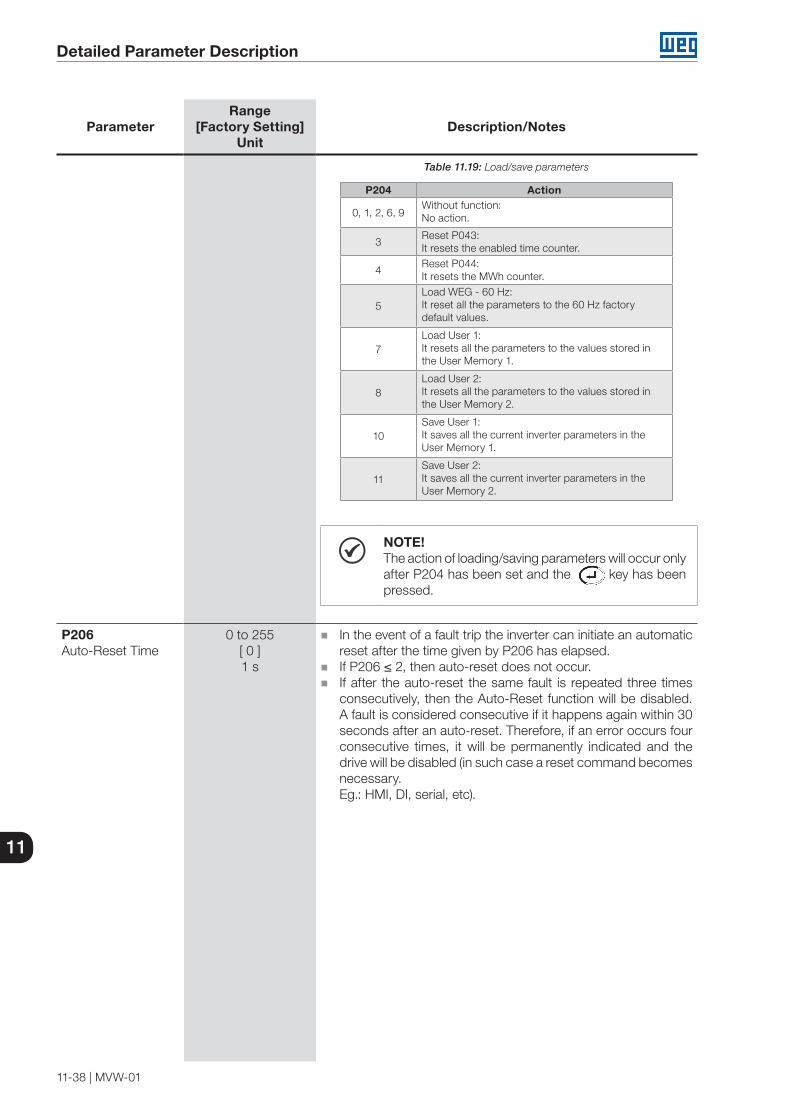
Detailed Parameter Description
11-38 | MVW-01
11
ParameterRange
[Factory Setting]Unit
Description/Notes
Table 11.19: Load/save parameters
P204 Action
0, 1, 2, 6, 9Without function:No action.
3Reset P043:It resets the enabled time counter.
4Reset P044:It resets the MWh counter.
5Load WEG - 60 Hz:It reset all the parameters to the 60 Hz factorydefault values.
7Load User 1:It resets all the parameters to the values stored in the User Memory 1.
8Load User 2:It resets all the parameters to the values stored in the User Memory 2.
10Save User 1:It saves all the current inverter parameters in the User Memory 1.
11Save User 2:It saves all the current inverter parameters in the User Memory 2.
NOTE!The action of loading/saving parameters will occur onlyafter P204 has been set and the key has been pressed.
P206Auto-Reset Time
0 to 255[ 0 ]1 s
In the event of a fault trip the inverter can initiate an automatic reset after the time given by P206 has elapsed.
If P206 ≤ 2, then auto-reset does not occur. If after the auto-reset the same fault is repeated three times
consecutively, then the Auto-Reset function will be disabled. A fault is considered consecutive if it happens again within 30 seconds after an auto-reset. Therefore, if an error occurs four consecutive times, it will be permanently indicated and the drive will be disabled (in such case a reset command becomes necessary. Eg.: HMI, DI, serial, etc).

Detailed Parameter Description
MVW-01 | 11-39
11
ParameterRange
[Factory Setting]Unit
Description/Notes
P208 (2)
Reference ScaleFactor
1 to 18000[ 1800 ]
1
It defines how the Speed Reference (P001) and the Motor Speed (P002) will be presented when the motor is running at synchronous speed.
To indicate the values in rpm: Adjust P208 for the synchronous speed, according to the table
below.
Table 11.20: Synchronous speed reference in rpm
Frequency Number of Motor Poles
SynchronousSpeed
50 Hz
2 30004 15006 10008 750
60 Hz
2 36004 18006 12008 900
In order to indicate other units:
The value shown can be calculated using the formulas:P002 = speed x P208 / synchronous speed x (10)P210
P001 = reference x P208 / synchronous speed x (10)P210
where:Speed = actual speed in rpm.Synchronous Speed = 120 x P403 / poles.Poles = 120 x P403 / P402, can be equivalent to 2, 4, 6, 8 or 10.Reference = speed reference in rpm.The number of places after the decimal point is defined in P210.
Example:If speed = synchronous speed = 1800, P207 = L/s, P208 = 900 (desired indication 90.0, therefore P210 = 1), thus the value shown will be: 90.0 L/s.
P209Motor Phase LossDetection
0 or 1[ 0 ]
-
Table 11.21: Motor phase loss
P209 Function0 Inactive1 Active
The Motor Phase Loss Detection trips indicating F076 (Motor Phase Loss) when the following conditions are simultaneously satisfied:I. P209 = active.II. Enabled inverter.III. Speed reference higher than 3 %.IV. Imax > 1.125 x Imin.Where: Imáx is the highest current of the three phases.
Imín is the lowest current of the three phases.
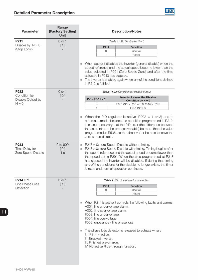
Detailed Parameter Description
11-40 | MVW-01
11
ParameterRange
[Factory Setting]Unit
Description/Notes
P211Disable by N = 0 (Stop Logic)
0 or 1[ 1 ]
-
Table 11.22: Disable by N = 0
P211 Function0 Inactive1 Active
When active it disables the inverter (general disable) when the speed reference and the actual speed become lower than the value adjusted in P291 (Zero Speed Zone) and after the time adjusted in P213 has elapsed.
The inverter is enabled again when any of the conditions defined in P212 is fulfilled.
P212Condition for Disable Output by N = 0
0 or 1[ 0 ]
-
Table 11.23: Condition for disable output
P212 (P211 = 1) Inverter Leaves the DisableCondition by N = 0
0 P001 (N*) > P291 or P002 (N) > P2911 P001 (N*) > 0
When the PID regulator is active (P203 = 1 or 3) and in automatic mode, besides the condition programmed in P212, it is also necessary that the PID error (the difference between the setpoint and the process variable) be more than the value programmed in P535, so that the inverter be able to leave the zero speed disable.
P213Time Delay forZero Speed Disable
0 to 999[ 0 ]1 s
P213 = 0: zero Speed Disable without timing. P213 > 0: zero Speed Disable with timing. Timing begins after
the speed reference and the actual speed become lower than the speed set in P291. When the time programmed at P213 has elapsed the inverter will be disabled. If during that timing any of the conditions for the disable no longer exists, the timer is reset and normal operation continues.
P214 (1) (6)
Line Phase LossDetection
0 or 1[ 1 ]
-
Table 11.24: Line phase loss detection
P214 Function0 Inactive1 Active
When P214 is active it controls the following faults and alarms:A001: line undervoltage alarm.A002: line overvoltage alarm.F003: line undervoltage.F004: line overvoltage.F006: unbalance / line phase loss.
The phase loss detector is released to actuate when:I. P214 = active.II. Enabled inverter.III. Finished pre-charge.IV. No active Ride-through function.
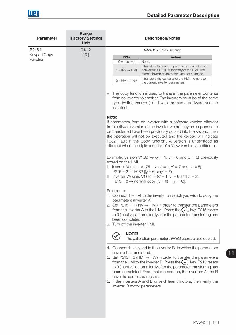
Detailed Parameter Description
MVW-01 | 11-41
11
ParameterRange
[Factory Setting]Unit
Description/Notes
P215 (1)
Keypad CopyFunction
0 to 2[ 0 ]
-
Table 11.25: Copy function
P215 Action0 = Inactive None.
1 = INV → HMIIt transfers the current parameter values to the nonvolatile EEPROM memory of the HMI. The current inverter parameters are not changed.
2 = HMI → INVIt transfers the contents of the HMI memory tothe current inverter parameters.
The copy function is used to transfer the parameter contents from ne inverter to another. The inverters must be of the same type (voltage/current) and with the same software version installed.
Note:If parameters from an inverter with a software version different from software version of the inverter where they are supposed to be transferred have been previously copied into the keypad, then the operation will not be executed and the keypad will indicate F082 (Fault in the Copy function). A version is understood as different when the digits x and y, of a Vx.yz version, are different.
Example: version V1.60 → (x = 1, y = 6 and z = 0) previously stored on the HMI.I. Inverter Version: V1.75 → (x’ = 1, y’ = 7 and z’ = 5).
P215 = 2 → F082 [(y = 6) ≠ (y’ = 7)].II. Inverter Version: V1.62 → (x’ = 1, y’ = 6 and z’ = 2).
P215 = 2 → normal copy [(y = 6) = (y’ = 6)].
Procedure:1. Connect the HMI to the inverter on which you wish to copy the
parameters (Inverter A).2. Set P215 = 1 (INV → HMI) in order to transfer the parameters
from the inverter A to the HMI. Press the key. P215 resets to 0 (inactive) automatically after the parameter transferring has been completed.3. Turn off the inverter HMI.
NOTE!The calibration parameters (WEG use) are also copied.
4. Connect the keypad to the inverter B, to which the parameters have to be transferred.
5. Set P215 = 2 (HMI → INV) in order to transfer the parameters from the HMI to the inverter B. Press the key. P215 resets to 0 (Inactive) automatically after the parameter transferring has been completed. From that moment on, the inverters A and B have the same parameters.
6. If the inverters A and B drive different motors, then verify the inverter B motor parameters.

Detailed Parameter Description
11-42 | MVW-01
11
ParameterRange
[Factory Setting]Unit
Description/Notes
7. To copy the parameters from the inverter A to more inverters, repeat the steps from 4 to 6.
Parameter Parameter
EEPROM
INVERTERB
INVERTERA
HMI→INVP215 = 2
Press
INV→HMIP215 = 1
Press
HMIHMI
EEPROM
Figure 11.24: Copy of the parameters from inverter A to B
It is not possible to operate the HMI while it is performing the Copy function.
Note: Inverters that received parameters from the other inverter must undergo the calibration process.
NOTE!The transfer process from one inverter to another must be performed/oriented by WEG technical assistance.

Detailed Parameter Description
MVW-01 | 11-43
11
ParameterRange
[Factory Setting]Unit
Description/Notes
P220 (1)
LOCAL/REMOTESelection Source
0 to 12[ 11 ]
-
It defines the origin of the command that will select between the Local situation and the Remote situation.
Table 11.26: Local/Remote selection
P220 Function0 Always Local.1 Always Remote.
2 HMI key (LOCAL default).
3 HMI key (REMOTE default).
4 Digital Inputs DI2...DI10 (P264...P272).5 Serial (Local Default).6 Serial (Remote Default).7 Fieldbus (Local Default).8 Fieldbus (Remote Default).9 Local PLC.10 Remote PLC.11 Graphic HMI (Local Default).12 Graphic HMI (Remote Default).
With the factory default settings the key selects between Local and Remote. After powering up the inverter, it will initiate in Local mode (Local default).
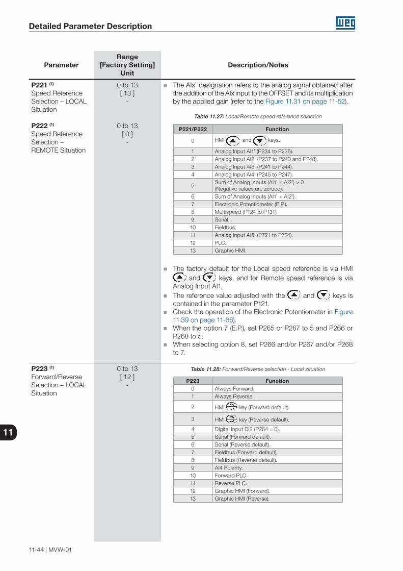
Detailed Parameter Description
11-44 | MVW-01
11
ParameterRange
[Factory Setting]Unit
Description/Notes
P221 (1)
Speed ReferenceSelection – LOCALSituation
P222 (1) Speed ReferenceSelection – REMOTE Situation
0 to 13[ 13 ]
-
0 to 13[ 0 ]
-
The AIx’ designation refers to the analog signal obtained after the addition of the AIx input to the OFFSET and its multiplication by the applied gain (refer to the Figure 11.31 on page 11-52).
Table 11.27: Local/Remote speed reference selection
P221/P222 Function
0 HMI and keys.
1 Analog Input AI1’ (P234 to P236).2 Analog Input AI2’ (P237 to P240 and P248).3 Analog Input AI3’ (P241 to P244).4 Analog Input AI4’ (P245 to P247).
5Sum of Analog Inputs (AI1’ + AI2’) > 0(Negative values are zeroed).
6 Sum of Analog Inputs (AI1’ + AI2’).7 Electronic Potentiometer (E.P.).8 Multispeed (P124 to P131).9 Serial.10 Fieldbus.11 Analog Input AI5’ (P721 to P724).12 PLC.13 Graphic HMI.
The factory default for the Local speed reference is via HMI and keys, and for Remote speed reference is via
Analog Input AI1. The reference value adjusted with the and keys is
contained in the parameter P121. Check the operation of the Electronic Potentiometer in Figure
11.39 on page 11-66). When the option 7 (E.P.), set P265 or P267 to 5 and P266 or
P268 to 5. When selecting option 8, set P266 and/or P267 and/or P268
to 7.
P223 (1)
Forward/ReverseSelection – LOCALSituation
0 to 13[ 12 ]
-
Table 11.28: Forward/Reverse selection - Local situation
P223 Function0 Always Forward.1 Always Reverse.
2 HMI key (Forward default).
3 HMI key (Reverse default).
4 Digital Input DI2 (P264 = 0).5 Serial (Forward default).6 Serial (Reverse default).7 Fieldbus (Forward default).8 Fieldbus (Reverse default).9 AI4 Polarity.10 Forward PLC.11 Reverse PLC.12 Graphic HMI (Forward).13 Graphic HMI (Reverse).

Detailed Parameter Description
MVW-01 | 11-45
11
ParameterRange
[Factory Setting]Unit
Description/Notes
P224 (1)
Start/Stop SelectionLOCAL Situation
0 to 5[ 0 ]
-
Table 11.29: Start/Stop selection – Local situation
P224 Function
0 HMI and keys.
1 Digital input DIx.2 Serial.3 Fieldbus.4 PLC.5 Graphic HMI.
Note: When the DIx inputs have the FORWARD/REVERSE function, the keys and HMI will remain inactive regardless of the value set in P224.
P225 (1)
Selection of JOGSource LOCALSituation
0 to 6[ 6 ]
-
Table 11.30: JOG selection – Local situation
P225 Function0 Disabled
1 HMI key.
2 Digital inputs DI3 to DI10 (P265 to P272).3 Serial.4 Fieldbus.5 PLC.6 Graphic HMI.
The speed reference value for JOG is provided by parameter P122.
P226 (1)
Selection ofDirection ofROTATIONREMOTE Situation
0 to 13[ 4 ]
-
Table 11.31: Selection of direction of rotation - Remote
P226 Function0 Always Forward.1 Always Reverse.
2 HMI key (Forward default).
3 HMI key (Reverse default).
4 Digital input DI2 (P264 = 0).5 Serial (Forward default).6 Serial (Reverse default).7 Fieldbus (Forward default).8 Fieldbus (Reverse default).9 AI4 polarity.10 Forward PLC.11 Reverse PLC.12 Graphic HMI (Forward Default).13 Graphic HMI (Reverse Default).

Detailed Parameter Description
11-46 | MVW-01
11
ParameterRange
[Factory Setting]Unit
Description/Notes
P227 (1)
Start/Stop Selection– REMOTE Situation
0 to 5[ 0 ]
-
Table 11.32: Start/Stop selection – Remote situation
P227 Function
0 HMI and keys.
1 Digital inputs DIx.2 Serial.3 Fieldbus.4 PLC.5 Graphic HMI.
Note: If the Digital Inputs are programmed for Forward Run / Reverse, Run, the and keys will remain disabled, regardless of the value programmed at P227.
P228 (1)
JOG Selection- REMOTE Situation
0 to 6 [ 1 ]
-
Table 11.33: JOG selection – Remote situation
P228 Function0 Inactive.1 HMI key.2 Digital inputs DI3 to DI10 (P265 to P272).3 Serial.4 Fieldbus.5 PLC.6 Graphic HMI.
The speed reference value for JOG is provided by parameter P122.

Detailed Parameter Description
MVW-01 | 11-47
11
LOCAL
LOCAL
REFERENCE
REMOTE
REFERENCE
LOCAL
COMMANDS
REMOTECOMMANDS
LOCAL/REMOTESELECTION
(P220)
REFERENCE
COMMANDSCOMMANDS
REFERENCE
FORWARD/REVERSE (P223)
START/STOP(P224)
REFERENCE(P222)
REMOTE
FORWARD/REVERSE
(P226)
START/STOP(P227)
JOG(P228)
JOG(P225)
REFERENCE(P221)
Figure 11.25: Local/Remote situation block diagram
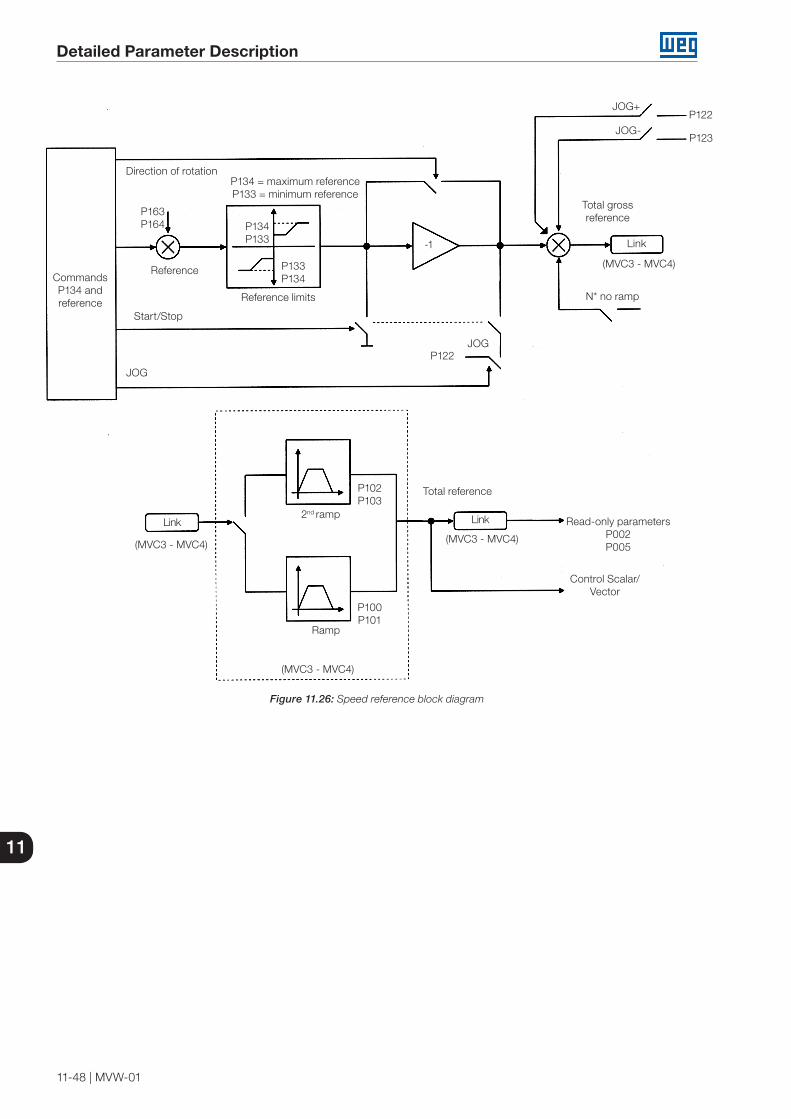
Detailed Parameter Description
11-48 | MVW-01
11
JOG+
JOG-
JOG
-1
Direction of rotation
Start/Stop
JOG
Reference limits
P134 P133
P133 P134Commands
P134 andreference
P122
P163P164
P134 = maximum referenceP133 = minimum reference
P123
P122
Reference
N* no ramp
Total grossreference
Link
(MVC3 - MVC4)
Link
(MVC3 - MVC4)
P102P103
P100P101
Total reference
Link
(MVC3 - MVC4)
(MVC3 - MVC4)
Ramp
2nd rampRead-only parameters
P002P005
Control Scalar/Vector
Figure 11.26: Speed reference block diagram
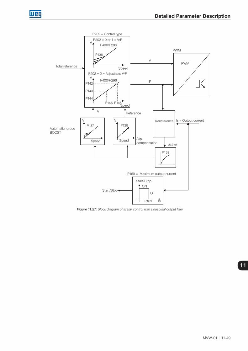
Detailed Parameter Description
MVW-01 | 11-49
11
Start/Stop
Start/Stop
P169 = Maximum output current
P136
P137 P138
P139
I active
P169 Is
P142
V
V V
V
V
V
F
P143
P144P146 P145
Reference
P400/P296
P400/P296
P202 = 2 = Adjustable V/F
P202 = 0 or 1 = V/F
P202 = Control type
Is = Output currentTransference
Speed
Speed
Speed Speed
PWM
PWM
ON
OFF
Total reference
Slipcompensation
Automatic torqueBOOST
Figure 11.27: Block diagram of scalar control with sinusoidal output filter
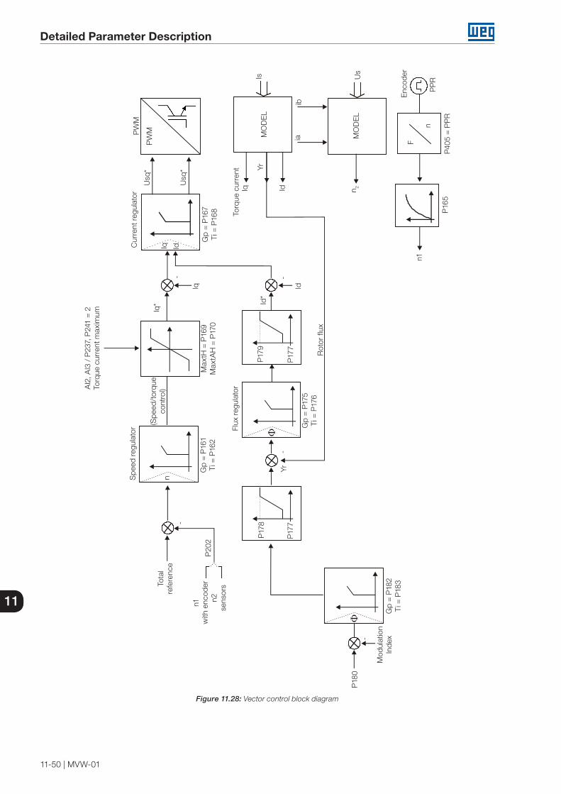
Detailed Parameter Description
11-50 | MVW-01
11
Enc
oder
PP
R
P405
= P
PR
n
F
P16
5
n1
MO
DE
LU
sn 2
ibia
Id
Yr
Iq
MO
DE
L
Torq
ue c
urre
nt
PW
MPW
MU
sq*
Usq
*
Cur
rent
reg
ulat
or
Gp
= P
167
Ti =
P16
8
IdIq
Iq
- -
-
-
Iq*
Max
tH =
P16
9M
axtA
H =
P17
0
AI2
, AI3
/ P
237,
P24
1 =
2To
rque
cur
rent
max
imum
(Spe
ed/t
orqu
eco
ntro
l)
Spe
ed r
egul
ator
Gp
= P
161
Ti =
P16
2
nTo
tal
refe
renc
e
n1w
ith e
ncod
ern2
sens
ors
P20
2
P18
0
Mod
ulat
ion
Inde
xG
p =
P18
2Ti
= P
183
P17
7
P17
8
Yr-
Gp
= P
175
Ti =
P17
6
Flux
reg
ulat
or
P17
9
P17
7Id
Id*
Rot
or fl
ux
Is
Figure 11.28: Vector control block diagram

Detailed Parameter Description
MVW-01 | 11-51
11
ParameterRange
[Factory Setting]Unit
Description/Notes
P231Actuation in the transition between Local and Remote for the HMIG
0 to 2[ 0 ]
-
P231 it defines the action to be taken by the inverter when the transition between LOCAL and REMOTE occurs for HMIG.
This parameter only actuates when P224 = 5 or P227 = 5.
Table 11.34: Stop mode selection
P231 Function0 It keeps the motor state1 It keeps the HMI state2 It turns off the motor *
(*) The option P231 = 2 (Turn off the motor) actuates according to the programming of P232 (Stop mode selection).
P232Stop ModeSelection
0 or 1[ 0 ]
-
Table 11.35: Stop mode selection
P232 Function0 Run/Stop1 General Disable
With the P232 setting, it is possible to select between the stop modes (START/STOP and GENERAL DISABLE) for the key or for the STOP function (via DIx).
NOTE!When the "DISABLE GENERAL" stop mode is programmed, only drive the motor if it is stopped or set the necessary time for which the inverter is disabled (COAST) in P725 to ensure the motor stop, or enable the Flystart function.
P233Analog Input Dead Zone
0 or 1[ 1 ]
-
It defines if the Dead Zone in the Analog Inputs is 0 = Inactive or 1 = Active.
If P233 = 0 (Inactive), the signal in the Analog Inputs acts on the Speed Reference from the minimum point: - (0 to 10) V/(0 to 20) mA/(4 to 20) mA:0 V/0 mA/4 mA.- (10 to 0) V/(20 to 0) mA /(20 to 4) mA:10 V/20 mA/20 mA.
If P233 = 1 (Active), the signal in the Analog Inputs has a dead zone, where the Speed Reference remains at the value of the Minimum Value (P133), even with the variation of the input signal.
a) P233 = 0 inactive
P134
Reference
dead zone
0 Signal Alx
P133
0 .................................10 V 0 .............................. 20 mA 4 mA ........................... 20 mA 10 V ...................................0 20 mA .................................0 20 mA ............................4 mA
Figure 11.29: Analog input dead zone inactive

Detailed Parameter Description
11-52 | MVW-01
11
ParameterRange
[Factory Setting]Unit
Description/Notes
P133
Alx signal0
P134
Reference
0 .................................10 V 0 .............................. 20 mA 4 mA ........................... 20 mA 10 V ...................................0 20 mA .................................0 20 mA ............................4 mA
Active dead zoneb) P233 = 1
Figure 11.30: Analog input dead zone active
If the analog input AI2 or AI4 is programmed for -10 V to +10 V (P246 = 4), curves identical to those of the Figure 11.30 on page 11-52, only when AI2 or AI4 is negative will the Direction of Rotation be inverted.
P234Analog Input AI1Gain
0.000 to 9.999[ 1.000 ]0.001
GAINP235P243P246P723
AIx
P234, P242, P245, P722
+
+
OFFSET (P236, P244, P247, P724)
AI1' - P018
AI3' - P020
AI4' - P021
AI5' - P028
Read
Figure 11.31: Analog inputs AI1, AI3, AI4 and AI5 block diagram
The internal values AI1’, AI3’, AI4’ and AI5’ are the results of the following equation:
AIx' = (AIx + OFFSET x 10 V) x gain 100
Example: AI1 = 5 V, OFFSET = -70 % and gain = 1.00:
AI1' = (5 + (-70) x10 V) x1 = -2 V
100
AI1’ = -2 V, meaning that the motor will run in reverse direction with a speed reference absolute value equal to 2 V.

Detailed Parameter Description
MVW-01 | 11-53
11
ParameterRange
[Factory Setting]Unit
Description/Notes
P235 (1)
Analog Input AI1Signal
0 to 3[ 0 ]
-
Table 11.36: Analog input AI1 signal
P235 Signal0 (0 to 10) V/(0 to 20) mA1 (4 to 20) mA2 (10 to 0) V/(20 to 0) mA3 (20 to 4) mA
When current signals are used in AI1 input, put S2. A switch on the MVC4 control card in the "ON" position.
For options 2 and 3 inverse reference is attained, that is, maximum speed is obtained with minimum reference.
P236Analog Input AI1Offset
-100.0 to +100.0[ 0.0 ]0.1%
Refer to the P234 description.
P237 (1)
Analog Input AI2Function
0 to 3[ 0 ]
-
Table 11.37: Analog input AI2 function
P237 Function0 P221/P2221 Without function2 Maximum torque current3 PID process variable
When the option 0 (P221/P222) is selected, AI2 is able to receive the speed reference, which will be subjected to the speed limits (P133 and P134) and ramp action (P100 to P103), providing that it has been programmed so in P221 and/or P222. Refer to the Figure 11.26 on page 11-48.
The option 3, process variable, defines the AI2 input as the PID regulator feedback signal (e.g., pressure or temperature sensor, etc.), provided that P524 = 0.
P238Analog Input AI2Gain
0.000 to 9.999[ 1.000 ]0.001
AI2
P239
OFFSET (P240)
P238
GAIN
FILTER (P248)
AI2' - P019
Read
Figure 11.32: Analog input AI2 block diagram
The internal value AI2’ is the results of the following equation:
AI2' = (AI2 + OFFSET x 10 V) x gain
100
For example: AI2 = 5 V, OFFSET = -70 % and gain = 1.00:
AI2' = (5 + (-70) x 10 V) x 1 = -2 V 100
AI2’ = -2 V, meaning that the motor will run in reverse direction
with a speed reference absolute value equal to 2 V.
Detailed Parameter Description
11-54 | MVW-01
11
ParameterRange
[Factory Setting]Unit
Description/Notes
AI2 has a variation range from -10 V to 10 V, no matter if P239 = 0 or 4, that is, an input voltage of 0 V corresponds in P019 = 50 %.
If it is necessary that 0 V correspond to P019 = 0 %, the following setting must be done:
P238 = 2
P240 = - 50 %
P239 (1)
Analog Input AI2Signal
0 to 4[ 0 ]
-
Table 11.38: Analog input AI2 signal
P239 Signal0 (0 to 10) V/(0 to 20) mA1 (4 to 20) mA2 (10 to 0) V/(20 to 0) mA3 (20 to 4) mA4 (-10 to +10) V
Set the S2.B switch on the MVC4 control board to the on position when a current signal is used at the analog input AI2.
Inverse reference is obtained with the options 2 and 3, i.e., the maximum speed is obtained with the minimum reference.
P240Analog Input AI2Offset
-100.0 to +100.0[ 0.0 ]0.1%
Refer to the P238 description.
P241 (1)
Analog Input AI3Function
(Isolated AnalogInput located onthe Optional Board EBB.Refer to theChapter 10 OPTIONAL ACCESSORIES AND BOARDS on page 10-1)
0 to 3 [ 0 ]
-
Table 11.39: Analog input AI3 function
P241 Function0 P221/P2221 Without function2 Maximum torque current3 PID process variable
When the option 0 (P221/P222) is selected, AI3 is able to receive the speed reference, which will be subjected to the speed limits (P133 and P134) and ramp action (P100 to P103), providing that it has been programmed so in P221 and/or P222. Refer to the Figure 11.26 on page 11-48.
The option 3, process variable, defines the AI3 input as the PID regulator feedback signal (e.g., pressure or temperature sensor, etc.), provided that P524 = 1.
P242Analog Input AI3Gain
0.000 to 9.999[ 1.000 ]0.001
Refer to the P234 description.

Detailed Parameter Description
MVW-01 | 11-55
11
ParameterRange
[Factory Setting]Unit
Description/Notes
P243 (1)
Analog Input AI3Signal
0 to 3[ 0 ]
-
Table 11.40: Analog input AI3 signal type
P243 Signal0 (0 to 10) V/(0 to 20) mA1 (4 to 20) mA2 (10 to 0) V/(20 to 0) mA3 (20 to 4) mA
Set the S4.1 switch on the EBB optional board to the on position when a current signal is used at the analog input AI3.
Inverse reference is obtained with the options 2 and 3, i.e., the maximum speed is obtained with the minimum reference.
P244Analog Input AI3Offset
-100.0 to +100.0[ 0.0 ]0.1%
Refer to the P234 description.
P245Analog Input AI4Gain
(14 bit Analog Inputlocated on the EBAOptional Board. Refer to theChapter 10 OPTIONAL ACCESSORIES AND BOARDS on page 10-1)
0.000 to 9.999[ 1.000 ]0.001
Refer to the P234 description.
P246 (1)
Analog Input AI4Signal
0 to 4[ 0 ]
-
Table 11.41: Analog input AI4 signal
P246 Signal
0 (0 to 10) V/ (0 to 20) mA
1 (4 to 20) mA
2 (10 to 0) V/ (20 to 0) mA
3 (20 to 4) mA
4 (-10 to +10) V
Inverse reference is obtained with the options 2 and 3, i.e., the maximum speed is obtained with the minimum reference.
When current signals are used in AI4 input, put S2.1 switch on the EBA optional card in the "ON" position.
P247Analog Input AI4Offset
-100.0 to +100.0[ 0.0 ]0.1 %
Refer to the P234 description.
P248Analog Input AI2Filter
0.0 to 16.0[ 0.0 ]0.1 s
It adjusts the analog input AI2 RC filter time constant. (Refer to the Figure 11.32 on page 11-53).
Detailed Parameter Description
11-56 | MVW-01
11
ParameterRange
[Factory Setting]Unit
Description/Notes
P251Analog Output AO1Function
0 to 21[ 2 ]
-
See Table 11.42 on page 11-57 for further details related to the function of analog outputs.
For values in the factory default (P251 = 2 and P252 = 1.000) AO1 = 10 V when Actual Speed = Maximum Speed (P134).
AO1 output may be located on the control card MVC4 (0 to 10) V or on the optional card EBB [AO1’, (0 to 20) mA/ (4 to 20) mA]. Refer to Chapter 10 OPTIONAL ACCESSORIES AND BOARDS on page 10-1. When EBB is used, the same signal is available for MVC4.
P252Analog Output AO1Gain
0.000 to 9.999[ 1.000 ]0.001
It adjusts the analog output AO1 gain. For a setting of P252 = 1.000, the AO1 value is adjusted according to the description of the analog output indication scales presented at P262 description.
P253Analog Output AO2Function
0 to 21[ 5 ]
-
Refer to Table 11.42 on page 11-57 for further details regarding the functions of the analog outputs.
With factory default values (P253 = 5 and P254 = 1.000) AO2 = 10 V when the output current is = 1.5 x P295.
The AO2 output can be located on the MVC4 control board (as 0 to 10 V) or on the option board EBB [AO2’, (0 to 20) mA/ (4 to 20) mA]. Refer to the Chapter 10 OPTIONAL ACCESSORIES AND BOARDS on page 10-1. When EBB is used, the same signal is available for MVC4.
P254Analog Output AO2Gain
0.000 to 9.999[ 1.000 ]0.001
It adjusts the analog output AO2 gain. For a setting of P254 = 1.000, the AO2 value is adjusted according to the description of the analog output indication scales presented at P262 description.
P255Analog Output AO3Function(Located on theEBA optionalboard)
0 to 21[ 2 ]
-
Refer to the Table 11.42 on page 11-57 for further details regarding the functions of the analog outputs.
With factory default values (P255 = 2 and P256 = 1.000) AO3 = 10 V when Actual Speed = Maximum Speed (P134).
For information on the AO3 output, refer to Chapter 10 OPTIONAL ACCESSORIES AND BOARDS on page 10-1.
P256Analog Output AO3Gain
0.000 to 9.999[ 1.000 ]0.001
It adjusts the analog output AO3 gain. For a setting of P256 = 1.000, the AO3 value is adjusted according to the description of the analog output indication scales presented at P262 description.
P257Analog Output AO4Function(Located on theEBA optionalboard)
0 to 21[ 5 ]
-
Refer to Table 11.42 on page 11-57 for further details regarding the functions of the analog outputs.
For values in the factory default (P257 = 5 and P258 = 1.000) AO4 = 10 V when Output Current = 1.5 x P295.
For information on the AO4 output, refer to Chapter 10 OPTIONAL ACCESSORIES AND BOARDS on page 10-1.
P258Analog Output AO4Gain
0.000 to 9.999[ 1.000 ]0.001
It adjusts the analog output AO4 gain. For a setting of P258 = 1.000, the AO4 value is adjusted according to the description of the analog output indication scales presented at P262 description.
Detailed Parameter Description
MVW-01 | 11-57
11
ParameterRange
[Factory Setting]Unit
Description/Notes
P259Analog Output AO5Function(isolated single-pole)
0 to 21[ 2 ]
-
Refer to Table 11.42 on page 11-57 for further details regarding the functions of the analog outputs.
For values in the factory default (P259 = 2 and P260 = 1.000) AO5 = 20 mA when Actual Speed = Maximum Speed (P134).
P260Analog Output AO5Gain
0.000 to 9.999[ 1.000 ]0.001
It adjusts the analog output AO5 gain, for a setting of P260 = 1.000, the AO5 value is adjusted according to the description of the analog output indication scales presented at P262 description.
P261Analog Output AO6Function(isolated single-pole)
0 to 21[ 5 ]
-
Refer to Table 11.42 on page 11-57 for further details regarding the functions of the analog outputs.
With factory default values (P261 = 5 and P262 = 1.000) AO6 = 20 mA when Output Current = 1.5 x P295.
P262Analog Output AO6Gain
0.000 to 9.999[ 1.000 ]0.001
It adjusts the analog output AO6 gain. For a setting of P262 = 1.000, the AO6 value is adjusted according to the description of the analog output indication scales presented here at P262 description.
Table 11.42: Analog output functions
Function P251(AO1)
P253(AO2)
P255(AO3)
P257(AO4)
P259(AO5)
P261(AO6)
FullScale (10 V)
SpeedReference
0 0 0 0 0 0 1 x P134
TotalReference
1 1 1 1 1 1 1 x P134
Actual Speed 2 2 2 2 2 2 1 x P134Not Used 3/4 3/4 3/4 3/4 3/4 3/4
Output Current(with 0.5 sec
filter)5 5 5 5 5 5 1.5 x P295
PID ProcessVariable
6 6 6 6 6 6 1 x P528
Output ActiveCurrent
7 7 7 7 7 7100 %
P295/P401
Real Power in theOutput
8 8 8 8 8 82 x P295 x
P296 x√ 3
PID Reference 9 9 9 9 9 9 1 x P528Not Used 10 10 10 10 10 10
TraceChannels 1 to 8
11 to 18
11 to 18
11 to 18
11 to 18
11 to 18
11 to 18
Sameparameter
chosenInverter
Temperature19 19 19 19 19 19 200 ºC
PLC 20 20 20 20 20 20Output Voltage 21 21 21 21 21 21 1 x P296
Detailed Parameter Description
11-58 | MVW-01
11
ParâmetroFaixa
[Ajuste de Fábrica]Unidade
Descrição / Observações
P251P253P255P257P259P261
Gain AOx
P252, P254, P256, P258, P260 and P262
Power
Active current
Output current
Torque current
Trace channels
Actual speed
Total reference
Speed reference
PID process variable
PID reference
Inverter temperature
Output voltage
PLC
Figure 11.33: Analog outputs block diagram
Analog output indication scales:- Full scale of 10 V for AO1 and AO2 outputs located on theMVC4 control board, and for AO3 and AO4 located on the EBAoptional board.-Full scale of 20 mA for AO1’ and AO2’ outputs located on theEBB optional board, and for AO5 and AO6 located on the MVC4control board.Speed reference (P001): full scale = P134.Total reference: full scale = P134.Actual speed (P002): full scale = P134.Output current: full scale = 1.5 x P295.PID process variable: full scale = 1.0 x P528.PID reference: full scale = 1.0 x P528.Inverter temperature = 200 ºC.Output power: full scale = 2.0 x P295 x P296 x √ 3 .
Detailed Parameter Description
MVW-01 | 11-59
11
ParâmetroFaixa
[Ajuste de Fábrica]Unidade
Descrição / Observações
P263 (1)
Digital Input DI1Function
P264 (1)
Digital Input DI2Function
P265 (1)
Digital Input DI3Function
P266 (1)
Digital Input DI4Function
P267 (1)
Digital Input DI5Function
P268 (1)
Digital Input DI6Function
P269 (1)
Digital Input DI7Function(Located on theoptional board)
P270 (1)
Digital Input DI8Function(Located on theoptional board)
0 to 3[ 0 (Not used) ]
-
0 or 1[ 0 (Forward/Reverse)]
-
0 to 26[ 0 (Not used) ]
-
0 to 26[ 0 (Not used) ]
-
0 to 26[ 3 (JOG) ]
-
0 to 26[ 6 (2nd ramp) ]
-
0 to 24[ 0 (Not used) ]
-
0 to 24[ 0 (Not used) ]
-
Refer to the Table 11.43 on page 11-62 and the Figure 11.34 on page 11-59 and Figure 11.37 on page 11-61 for further details regarding the functions of the digital inputs.
The digital input status can be monitored at the parameter P012.Notes:‘Increase EP (Electronic Potentiometer) is active when DI3 or DI5 are closed = +24 V.‘Decrease EP’ (Electronic Potentiometer) is active when DI4 orDI6 are open = 0 V.‘LOCAL/REMOTE’ = 0 V/24 V in the digital input respectively.DI8 digital input is linked to the input for ‘Motor Thermistor’ (PTC) present on the EBA/EBB optional cards:
PTC
XC4/XC5:
EBA/EBB DI8 (P270 = 16)
2
3
Inactive /without error
Inactive /without error Active / E32
Inactive /without error
Active / E32Active / E32Temperature
decrease
1k6 3k9
Temperatureincrease
PTC resistancevariation in ohms (Ω)
Figure 11.34: DI8 as a PTC input

Detailed Parameter Description
11-60 | MVW-01
11
ParâmetroFaixa
[Ajuste de Fábrica]Unidade
Descrição / Observações
P271 (1)
Digital Input DI9Function
P272 (1)
Digital Input DI10Function
0 to 24[ 0 (Not used) ]
-
0 to 24[ 0 (Not used) ]
-
In order to use the DI8 as a normal digital input, program the designated function at P270, and connect a resistor, ranging from 270 to 1600 Ω, in series with the contact:
XC4/XC5:
DI8
(P270)EBA/EBB
2
3
R = 270 to 1600 Ω
Contact Contact DI8Open Deactivated
Closed Activated
Figure 11.35: DI8 as a normal digital input
The function ‘Load User via DIx’ allows the selection between the user memories 1 and 2, performing actions similar to the setting of P204 = 7 or 8; however, the user memories are loaded by the transition of a digital input programmed for that function.
When the DIx state changes from low to high level (transition from 0 V to 24 V), and P265 to P270 = 20, the user memory 1 is loaded, provided that the contents of the inverter actual parameters had been previously transferred to the user memory 1 (P204 = 10).
When the DIx state changes from high to low level (transition from 24 V to 0 V) and P265 to P270 = 20, the user memory 2 is loaded, provided that the contents of the inverter actual parameters had been previously transferred to the user memory 2 (P204 = 11).
Inverterparameters
User 1
User 2P204 = 11
P204 = 10
P265 to P270 (DIx) = 20
DIx = 0 VP265 to P270 (DIx) = 20
DIx = 24V DIx = 0 V
DIx = 24 V
Figure 11.36: Details on the load user via DIx operation
NOTE!Make sure that when using those functions the parameter sets (user memory 1 and 2) be entirely compatible with the application (motors, Start/Stop commands, etc.). It will not be possible to load the user memory with the motor enabled.If two parameter sets from different motors were savedin the user memories 1 and 2, the correct motor currentvalues for each user memory must be adjusted at theparameters P156, P157 and P158.
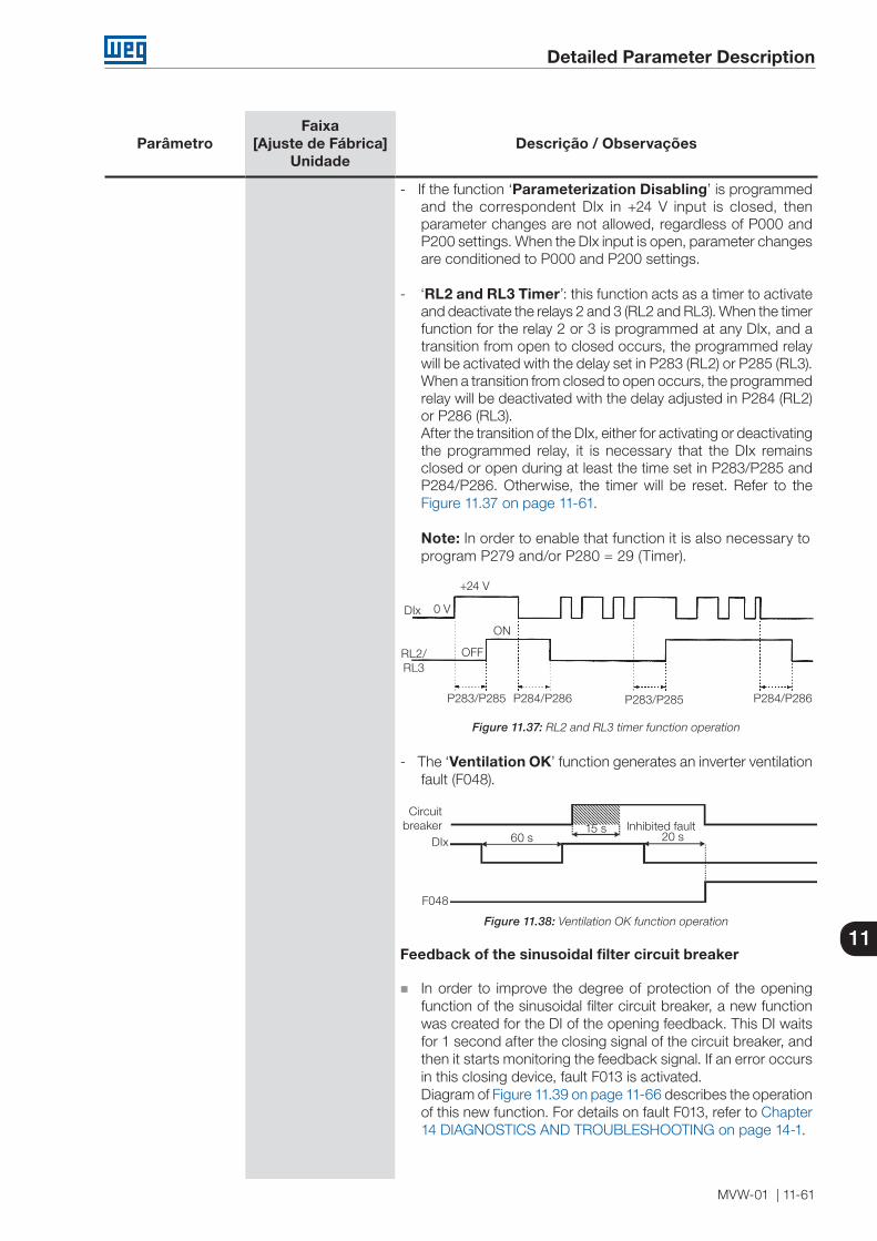
Detailed Parameter Description
MVW-01 | 11-61
11
ParâmetroFaixa
[Ajuste de Fábrica]Unidade
Descrição / Observações
- If the function ‘Parameterization Disabling’ is programmed and the correspondent DIx in +24 V input is closed, then parameter changes are not allowed, regardless of P000 and P200 settings. When the DIx input is open, parameter changes are conditioned to P000 and P200 settings.
- ‘RL2 and RL3 Timer’: this function acts as a timer to activate and deactivate the relays 2 and 3 (RL2 and RL3). When the timer function for the relay 2 or 3 is programmed at any DIx, and a transition from open to closed occurs, the programmed relay will be activated with the delay set in P283 (RL2) or P285 (RL3). When a transition from closed to open occurs, the programmedrelay will be deactivated with the delay adjusted in P284 (RL2)or P286 (RL3).After the transition of the DIx, either for activating or deactivatingthe programmed relay, it is necessary that the DIx remains closed or open during at least the time set in P283/P285 and P284/P286. Otherwise, the timer will be reset. Refer to the Figure 11.37 on page 11-61.
Note: In order to enable that function it is also necessary toprogram P279 and/or P280 = 29 (Timer).
+24 V
0 VDIx
RL2/RL3
ON
OFF
P283/P285 P284/P286 P283/P285 P284/P286
Figure 11.37: RL2 and RL3 timer function operation
- The ‘Ventilation OK’ function generates an inverter ventilation fault (F048).
DIx 60 s 20 s15 s
Circuitbreaker Inhibited fault
F048
Figure 11.38: Ventilation OK function operation
Feedback of the sinusoidal filter circuit breaker
In order to improve the degree of protection of the opening function of the sinusoidal filter circuit breaker, a new function was created for the DI of the opening feedback. This DI waits for 1 second after the closing signal of the circuit breaker, and then it starts monitoring the feedback signal. If an error occurs in this closing device, fault F013 is activated.Diagram of Figure 11.39 on page 11-66 describes the operation of this new function. For details on fault F013, refer to Chapter 14 DIAGNOSTICS AND TROUBLESHOOTING on page 14-1.

Detailed Parameter Description
11-62 | MVW-01
11
Table 11.43: Digital input functions
Parameter DIx Function
P263(DI1)
P264(DI2)
P265(DI3)
P266(DI4)
P267(DI5)
P268(DI6)
P269(DI7)
P270(DI8)
P271(DI9)
P272(DI10)
Not used 0 -0, 7, 17 and 18
0, 17 and 18
0, 17 and 18
0, 17 and 18
0, 5, 7, 9, 16, 17 and
18
0, 5, 7, 9, 17 and 18
0, 5, 7, 9, 17 and 18
0, 5, 7, 9, 17 and 18
Start/Stop 1 - - - - - - - - -General Enable 2 - 2 2 2 2 2 2 2 2
Fast Stop 3 - - - 8 8 8 8 8 8Forward/Reverse - 0 - - - - - - - -
Local/Remote - 1 1 1 1 1 1 1 1 1JOG - - 3 3 3 3 3 3 3 3
No External Fault - - 4 4 4 4 4 4 4 4Increase EP - - 5 - 5 - - - - -Decrease EP - - - 5 - 5 - - - -
2nd Ramp - - 6 6 6 6 6 6 6 6Multispeed (MSx) - - - 7 7 7 - - - -
Forward Run - - 8 - - - - - - -Reverse Run - - - 8 - - - - - -
Sinusoidal Filter Circuit Breaker
- - 9 9 9 9 - - - -
JOG+ - - 10 10 10 10 10 10 10 10JOG- - - 11 11 11 11 11 11 11 11Reset - - 12 12 12 12 12 12 12 12
Fieldbus - - 13 13 13 13 13 13 13 13Start - - 14 - 14 - 14 - - -Stop - - - 14 - 14 - 14 14 14
Manual/Automatic - - 15 15 15 15 15 15 15 15No External Alarm - - 16 16 16 16 - - 16 16Motor Thermistor - - - - - - - 16 - -
Parameterization Disabling - - 19 19 19 19 19 19 - -Load User 1/2 - - 20 20 20 20 20 20 - -
RL2 Timer - - 21 21 21 21 21 21 - -RL3 Timer - - 22 22 22 22 22 22 - -
No Motor Fault - - - - - - - - 19 19No Motor Alarm - - - - - - - - 20 20No Alarm in the
Redundant VentilationSet A
- - 23 23 23 23 - - 21 21
No Alarm in theRedundant Ventilation
Set B- - 24 24 24 24 - - 22 22
Initiates SynchronousTransfer
- - 25 25 25 25 23 23 23 23
Ventilation OK - - 26 26 26 26 24 24 24 24
NOTE!In order that Start/Stop works, program also P224 and/or P227 = 1.The selection of P265 or P267 = 5, and P266 or P268 = 5, also requires the programming of P221 and/or P222 = 7.The programming of P266 and/or P267 and/or P268 = 7 also requires the programming of P221 and/or P222 = 8.
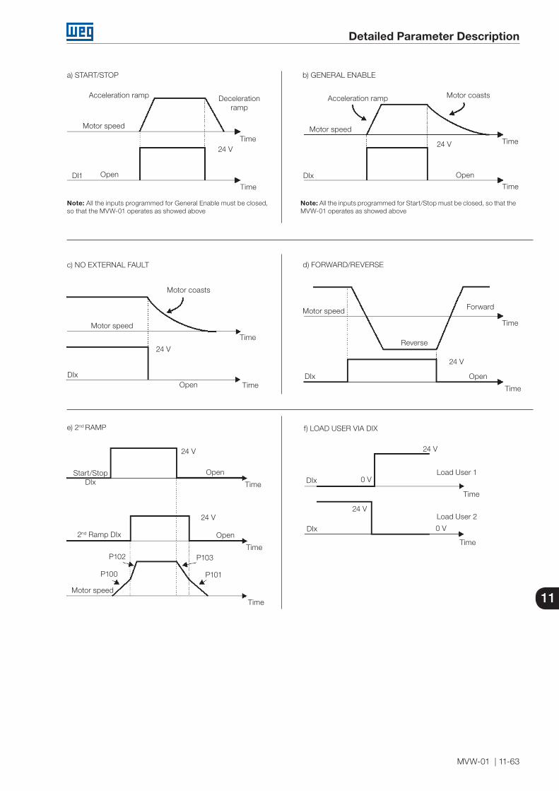
Detailed Parameter Description
MVW-01 | 11-63
11
DI1
24 V
Motor speed
Decelerationramp
DIx Open
Time
Motor speed
Motor coasts
Time
TimeTime24 V
Open
24 V
Time
Time
Motor speed
DIx Open
24 V
Time
Time
Motor speed
DIx
Forward
Open
Open
24 V
Time
Time
24 V
Time
P102
P100
Start/StopDIx
2nd Ramp DIx
e) 2nd RAMP
Acceleration ramp Acceleration ramp
Motor speed
Open
Reverse
d) FORWARD/REVERSEc) NO EXTERNAL FAULT
a) START/STOP b) GENERAL ENABLE
Motor coasts
P103
P101
Note: All the inputs programmed for General Enable must be closed, so that the MVW-01 operates as showed above
f) LOAD USER VIA DIX
Time
Time
Load User 1
Load User 2
DIx
24 V
24 V
DIx
0 V
0 V
Note: All the inputs programmed for Start/Stop must be closed, so that the MVW-01 operates as showed above
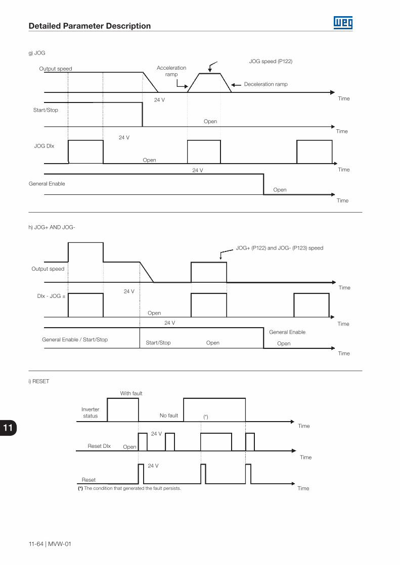
Detailed Parameter Description
11-64 | MVW-01
11
Time
Output speed
24 V
24 V
Start/Stop
JOG speed (P122)
Deceleration ramp
24 V
JOG DIx
General Enable
Open
Open
Open
Accelerationramp
g) JOG
With fault
24 V
General Enable / Start/StopOpen
Time24 V
Time
Time
24 V
No fault
Reset
Reset DIx Open
Output speed
Inverterstatus (*)
JOG+ (P122) and JOG- (P123) speed
Time
Time
Time
Time
Time
Time
(*) The condition that generated the fault persists.
24 V
Open
DIx - JOG ±
i) RESET
Start/Stop Open
General Enable
h) JOG+ AND JOG-
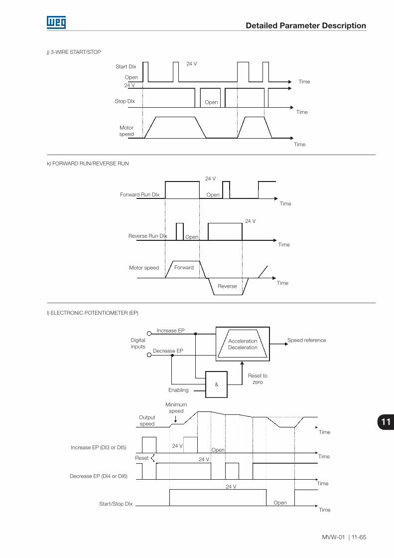
Detailed Parameter Description
MVW-01 | 11-65
11
Time
Time
24 V
Motorspeed
Open
Time
24 V
Time
Time
24 V
OpenReverse Run DIx
Forward Run DIx
Motor speed Forward
Time
Outputspeed
24 V
Open
24 V
Start/Stop DIx
AccelerationDeceleration
Speed reference
Reset tozero
Decrease EP
&
Increase EP
24 V
Open
Open
Reverse
Enabling
Minimumspeed
Reset
k) FORWARD RUN/REVERSE RUN
l) ELECTRONIC POTENTIOMETER (EP)
Digitalinputs
Decrease EP (DI4 or DI6)
Increase EP (DI3 or DI5)
Stop DIx
Start DIx
j) 3-WIRE START/STOP
Time
24 V
OpenTime
Time
Time
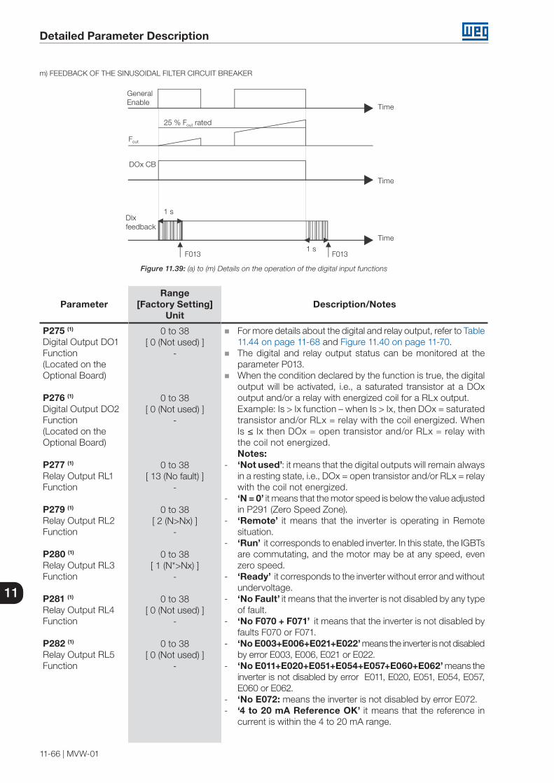
Detailed Parameter Description
11-66 | MVW-01
11
m) FEEDBACK OF THE SINUSOIDAL FILTER CIRCUIT BREAKER
General Enable
25 % Fout rated
Fout
1 s
1 sF013F013
DOx CB
Dlx feedback
Time
Time
Time
Figure 11.39: (a) to (m) Details on the operation of the digital input functions
ParameterRange
[Factory Setting]Unit
Description/Notes
P275 (1)
Digital Output DO1Function(Located on theOptional Board)
P276 (1)
Digital Output DO2Function(Located on theOptional Board)
P277 (1)
Relay Output RL1Function
P279 (1)
Relay Output RL2Function
P280 (1)
Relay Output RL3Function
P281 (1)
Relay Output RL4Function
P282 (1)
Relay Output RL5Function
0 to 38[ 0 (Not used) ]
-
0 to 38[ 0 (Not used) ]
-
0 to 38[ 13 (No fault) ]
-
0 to 38[ 2 (N>Nx) ]
-
0 to 38[ 1 (N*>Nx) ]
-
0 to 38[ 0 (Not used) ]
-
0 to 38[ 0 (Not used) ]
-
For more details about the digital and relay output, refer to Table 11.44 on page 11-68 and Figure 11.40 on page 11-70.
The digital and relay output status can be monitored at the parameter P013.
When the condition declared by the function is true, the digital output will be activated, i.e., a saturated transistor at a DOx output and/or a relay with energized coil for a RLx output.Example: Is > Ix function – when Is > Ix, then DOx = saturatedtransistor and/or RLx = relay with the coil energized. When Is ≤ Ix then DOx = open transistor and/or RLx = relay with the coil not energized.Notes:
- ‘Not used’: it means that the digital outputs will remain always in a resting state, i.e., DOx = open transistor and/or RLx = relay with the coil not energized.
- ‘N = 0’ it means that the motor speed is below the value adjusted in P291 (Zero Speed Zone).
- ‘Remote’ it means that the inverter is operating in Remote situation.
- ‘Run’ it corresponds to enabled inverter. In this state, the IGBTs are commutating, and the motor may be at any speed, even zero speed.
- ‘Ready’ it corresponds to the inverter without error and without undervoltage.
- ‘No Fault’ it means that the inverter is not disabled by any type of fault.
- ‘No F070 + F071’ it means that the inverter is not disabled by faults F070 or F071.
- ‘No E003+E006+E021+E022’ means the inverter is not disabled by error E003, E006, E021 or E022.
- ‘No E011+E020+E051+E054+E057+E060+E062’ means the inverter is not disabled by error E011, E020, E051, E054, E057, E060 or E062.
- ‘No E072: means the inverter is not disabled by error E072.- ‘4 to 20 mA Reference OK’ it means that the reference in
current is within the 4 to 20 mA range.
Detailed Parameter Description
MVW-01 | 11-67
11
ParameterRange
[Factory Setting]Unit
Description/Notes
- ‘Forward’ it means that when the motor is rotating in the forward direction, the DOx = saturated transistor and/or RLx = relay with the coil energized. When the motor is rotating in the reverse direction, the DOx = open transistor and/or RLx = relay with the coil not energized.
- ‘Pre-charge OK’ it means that the DC Link voltage is above the pre-charge voltage level.
- ‘Fault’ it means that the inverter is disabled by a fault.- ‘N > Nx and Nt > Nx’ it means that both the conditions must be
satisfied, so that DOx = saturated transistor and/or RLx = relay with the coil energized. In order that the digital outputs go back to the resting state, i.e., DOx = open transistor and/or RLx = relay with the coil not energized, it is necessary that only the condition N > Nx not be satisfied anymore (regardless of the Nt > Nx condition).
Definition of the symbols used with the functions:- N = P002 (Motor Speed).- N* = P001 (Speed Reference).- Nx = P288 (Nx Speed) - It is a reference point of the speed
selected by the user.- Ny = P289 (Ny Speed) - It is a reference point of the speed
selected by the user.- Ix = P290 (Ix Current) - It is a reference point of the current
selected by the user.- Is = P003 (Motor Current) Torque = P009 (Motor Torque)- Tx = P293 (Tx Torque) - It is a reference point of the torque
selected by the user. Note: Function not implemented in this software version.- VPx = P533 (PVx Process Variable) - It is a reference point of
the process variable selected by the user.- VPy = P534 (Variável Processo y) - It is a reference point of the
process variable selected by the user.- Nt = Total Reference (refer to the Figure 11.26 on page 11-48).- Safety Stop.- Sinusoidal Filter Circuit Breaker.- Normal Slave.
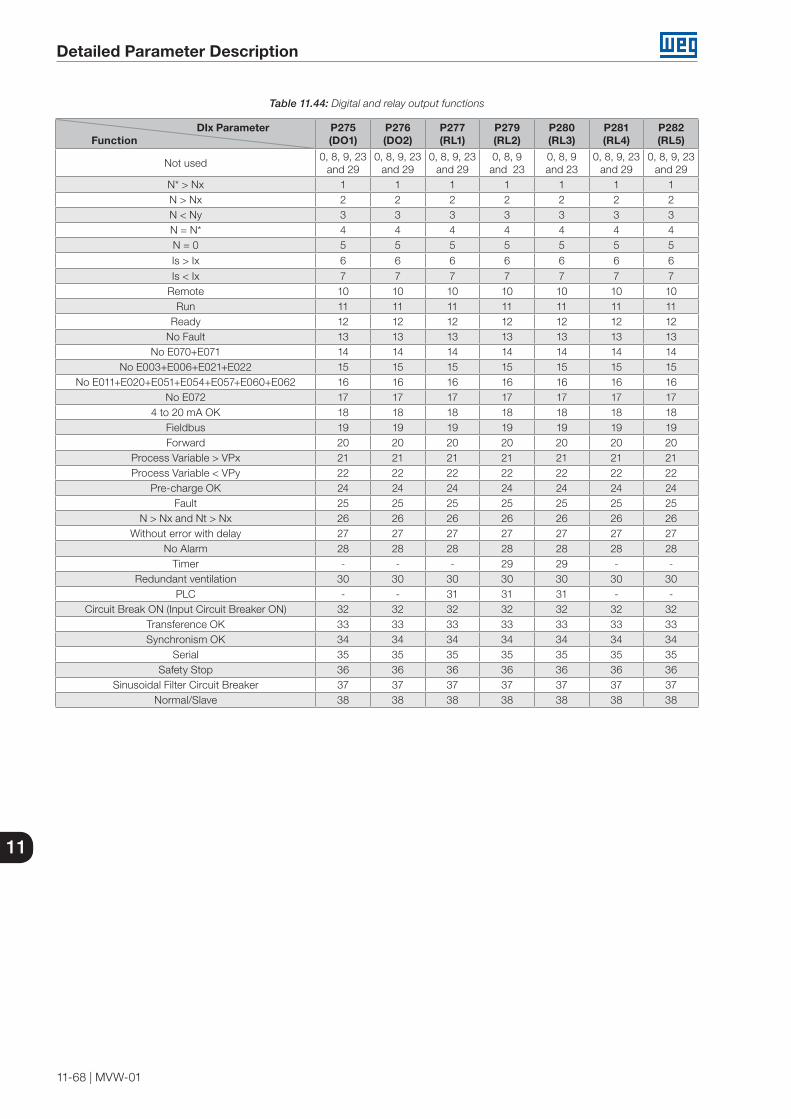
Detailed Parameter Description
11-68 | MVW-01
11
Table 11.44: Digital and relay output functions
DIx Parameter Function
P275(DO1)
P276(DO2)
P277(RL1)
P279(RL2)
P280(RL3)
P281(RL4)
P282(RL5)
Not used0, 8, 9, 23
and 290, 8, 9, 23
and 290, 8, 9, 23
and 290, 8, 9 and 23
0, 8, 9 and 23
0, 8, 9, 23 and 29
0, 8, 9, 23 and 29
N* > Nx 1 1 1 1 1 1 1N > Nx 2 2 2 2 2 2 2N < Ny 3 3 3 3 3 3 3N = N* 4 4 4 4 4 4 4N = 0 5 5 5 5 5 5 5Is > Ix 6 6 6 6 6 6 6Is < Ix 7 7 7 7 7 7 7
Remote 10 10 10 10 10 10 10Run 11 11 11 11 11 11 11
Ready 12 12 12 12 12 12 12No Fault 13 13 13 13 13 13 13
No E070+E071 14 14 14 14 14 14 14No E003+E006+E021+E022 15 15 15 15 15 15 15
No E011+E020+E051+E054+E057+E060+E062 16 16 16 16 16 16 16No E072 17 17 17 17 17 17 17
4 to 20 mA OK 18 18 18 18 18 18 18Fieldbus 19 19 19 19 19 19 19Forward 20 20 20 20 20 20 20
Process Variable > VPx 21 21 21 21 21 21 21Process Variable < VPy 22 22 22 22 22 22 22
Pre-charge OK 24 24 24 24 24 24 24Fault 25 25 25 25 25 25 25
N > Nx and Nt > Nx 26 26 26 26 26 26 26Without error with delay 27 27 27 27 27 27 27
No Alarm 28 28 28 28 28 28 28Timer - - - 29 29 - -
Redundant ventilation 30 30 30 30 30 30 30PLC - - 31 31 31 - -
Circuit Break ON (Input Circuit Breaker ON) 32 32 32 32 32 32 32Transference OK 33 33 33 33 33 33 33Synchronism OK 34 34 34 34 34 34 34
Serial 35 35 35 35 35 35 35Safety Stop 36 36 36 36 36 36 36
Sinusoidal Filter Circuit Breaker 37 37 37 37 37 37 37Normal/Slave 38 38 38 38 38 38 38

Detailed Parameter Description
MVW-01 | 11-69
11
Time
Time
TimeTime
Time Time
TimeTime
N
Relay/Transistor OFF
ON
a) N > Nx
OFF
NN*
Nx (P288)N
ON
OFF
ON
OFF
ON
OFFRelay/Transistor Relay/Transistor
OFF
Is
OFF
Time
N*
Relay/Transistor
OFF
ON
OFF
Is
Relay/Transistor
ON
OFF
ON
b) N < Ny
Ny (P289)
Relay/Transistor ON
Time
Nx (P288)
c) N = N* d) Is > Ix
ON
OFFOFF
Torque on the motor (P009)
Relay/Transistor
ONON
OFF
Relay/Transistor
f) Is < Ixe) N* > Nx
Torque on the motor (P009)
Tx (P293)
Ix (P290)
Ix (P290)
Tx (P293)
TimeTime
Time Time
h) Torque < Txg) Torque < Tx
N* N*

Detailed Parameter Description
11-70 | MVW-01
11
TimeTime
TimeTime
Time
Time
Time
Time
Relay/Transistor ON
No Fault
OFF
P291
Relay/Transistor
OFF OFFON
Relay/Transistor
ON ONOFF
Time
Time
2 mA
Speed
With fault
l) N = 0k) 4 to 20 mA reference
Ref
o) Process variable Y < VPy
Time
OFF
ONON
VPy (P534)
Relay/Transistor
Process variable
m) Process variable X > VPx
ON
OFF
Time
VPx (P533)
Process variable
Relay/Transistor
OFF Relay/Transistor
ON ONOFF
Time
Pre-chargelevel
DC link
n) Pre-charge OK
i) N > Nx and Nt > Nx
Nt N
Relay/TransistorOFF
ON
OFF
Time
Nx (P288)
j) No external error
Figure 11.40: (a) to (o) Details on the operation of the digital output functions

Detailed Parameter Description
MVW-01 | 11-71
11
ParameterRange
[Factory Setting]Unit
Description/Notes
P283RL2 On Time
0.0 to 300.0[ 0.0 ]0.1 s
It is used with the output relay function:Relay 2 timer.
P284RL2 Off Time
0.0 to 300.0[ 0.0 ]0.1 s
It is used with the output relay function:Relay 2 timer.
P285RL3 On Time
0.0 to 300.0[ 0.0 ]0.1 s
It is used with the output relay function:Relay 3 timer.
P286RL3 Off Time
0.0 to 300.0[ 0.0 ]0.1 s
It is used with the output relay function:Relay 3 timer.
P288 (2)
Nx Speed
P289 (2)
Ny Speed
0 to P134[ 120 ]1 rpm
0 to P134[ 1800 ]1 rpm
It is used with the output relay function:N* > Nx, N > Nx and N < Ny.
P290 (5)
Ix Current0 to 2.0xP295[ 1.0xP295 ]
0.1 A (<100) -1 A (>99.9)
It is used with the output relay function:Is > Ix and Is < Ix.
P291Zero Speed Zone
1 to 100[ 1 ]1 %
It is used with the output relay function:N = 0 and Zero Speed Disable (Refer to P211 and P212descriptions).
P292N = N* Band(Reached Speed)
1 to 100[ 1 ]1 %
It is used with the output relay function:N = N*.
P293Tx Torque
0 to 200 (P401)100 (P401)
%
Function not implemented in this software version.
P294Overload Class
0 to 2[ 0 ]
-
Table 11.45: Overload class
P294 Operation Overload0 Normal Overload Duty (ND) 115 % *1 Heavy Overload Duty (HD) 150 % *2 Maximum Current (MX) 100 % *
* For 60 s / 10 min

Detailed Parameter Description
11-72 | MVW-01
11
ParameterRange
[Factory Setting]Unit
Description/Notes
P295 (1)
Inverter RatedCurrent
0 to 143[ According to the
inverter ratedcurrent ]
A
Table 11.46: Current available models
P295 Rated Current G1 P295 Rated
Current G2 P295 Rated Current G2
0 32 A 70 54 A 122 627 A1 53 A 71 58 A 123 631 A2 70 A 72 67 A 124 664 A3 80 A 73 73 A 125 713 A4 85 A 74 78 A 126 740 A5 94 A 75 86 A 127 741 A6 100 A 76 91 A 128 779 A7 110 A 77 92 A 129 816 A8 112 A 78 96 A 130 835 A9 120 A 79 108 A 131 934 A10 130 A 80 109 A 132 941 A11 138 A 81 113 A 133 1069 A12 140 A 82 114 A 134 1087 A13 150 A 83 128 A 135 1234 A14 160 A 84 131 A 136 1254 A15 162 A 85 139 A 137 1425 A16 165 A 86 144 A 138 1482 A17 170 A 87 151 A 139 1632 A18 175 A 88 152 A 140 1881 A19 186 A 89 176 A 141 2138 A20 188 A 90 177 A 142 2508 A21 210 A 91 180 A 143 2850 A22 235 A 92 181 A23 250 A 93 204 A24 265 A 94 205 A25 280 A 95 212 A26 300 A 96 216 A27 310 A 97 237 A28 357 A 98 241 A29 375 A 99 251 A30 386 A 100 260 A31 450 A 101 276 A32 475 A 102 283 A33 490 A 103 294 A34 500 A 104 295 A35 560 A 105 322 A36 580 A 106 330 A37 1064 A 107 332 A38 712 A 108 348 A39 880 A 109 376 A40 950 A 110 390 A41 1178 A 111 405 A42 200 A 112 410 A43 125 A 113 440 A44 536 A 114 458 A45 1072 A 115 481 A46 1340 A 116 494 A47 1424 A 117 517 A48 1760 A 118 538 A49 1900 A 119 561 A50 2356 A 120 565 A51 301 A 121 607 A

Detailed Parameter Description
MVW-01 | 11-73
11
ParameterRange
[Factory Setting]Unit
Description/Notes
P296 (1)
Rated Voltage0 to 6
[ According to theinverter rated
voltage ]V
Table 11.47: Voltage available models
P296 Inverter Rated Voltage0 220 V *1 380 V *2 2300 V3 3300 V4 4160 V5 6900 V6 4600 V
* Use of WEG.
For inverters of rated voltage of 6000 V, 6300 V and 6600 V, you must set P296 = 5.
ATTENTION!Adjust P296 according to the input AC voltage to be used!
P303Skipped Speed 1
P304Skipped Speed 2
P305Skipped Speed 3
P306Skipped Range
P133 to P134[ 600 ]1rpm
P133 to P134[ 900 ]1rpm
P133 to P134[ 1200 ]1rpm
0 to 750[ 0 ]
1rpm
2 x P306
P30
3
P30
4
P30
5
P303
P304
P305
2 x P306
Speed reference
Motor speed
Figure 11.41: Skipped speed curve
It avoids permanent motor operation at speeds in which, for instance, the mechanical system enters into resonance causing high vibration or noise levels.
The passage through the skipped range (2 x P306) occurs through the acceleration and deceleration ramps.
The function does not operate properly if two bands of skipped speed overlap.
P308 (1) Inverter Address
1 to 30[ 1 ]
-
It sets the inverter address for serial communication. Refer to the Section 13.2 WEGBUS SERIAL on page 13-12.

Detailed Parameter Description
11-74 | MVW-01
11
ParameterRange
[Factory Setting]Unit
Description/Notes
P309 (1) Fieldbus
0 to 13[ 0 ]
-
0 = Inactive Fieldbus. 1 to 6 = define the fieldbus standard to be used (Profibus DP
or DeviceNet) and the number of variables to be exchanged with the master. Refer to the Item 13.1.6 Fieldbus Application/MVW-01 Related Parameters on page 13-7.
It is only applicable for the Profibus DP or DeviceNet optional kits. For P309 = 10, refer to the DeviceNet Drive Profile guide.
Table 11.48: Type of fieldbus protocol
P309 Type0 Inactive1 Profibus-DP 2 I/O2 Profibus-DP 4 I/O3 Profibus-DP 6 I/O4 DeviceNet 2 I/O5 DeviceNet 4 I/O6 DeviceNet 6 I/O7 Modbus-RTU 2 I/O8 Modbus-RTU 4 I/O9 Modbus-RTU 6 I/O10 DeviceNet Drive Profile11 Ethernet/IP 2 I/O12 Ethernet/IP 4 I/O13 Ethernet/IP 6 I/O
P312Type of SerialProtocol
0 to 11[ 0 ]
-
Table 11.49: Type of serial protocol
P312 Type0 WEG Protocol1 Modbus-RTU, 9600 bps, no parity2 Modbus-RTU, 9600 bps, odd parity3 Modbus-RTU, 9600 bps, even parity4 Modbus-RTU, 19200 bps, no parity5 Modbus-RTU, 19200 bps, odd parity6 Modbus-RTU, 19200 bps, even parity7 Modbus-RTU, 38400 bps, no parity8 Modbus-RTU, 38400 bps, odd parity9 Modbus-RTU, 38400 bps, even parity10 WEG Protocol, 19200 bps11 WEG Protocol, 38400 bps
It defines the type of protocol used for the serial communication.
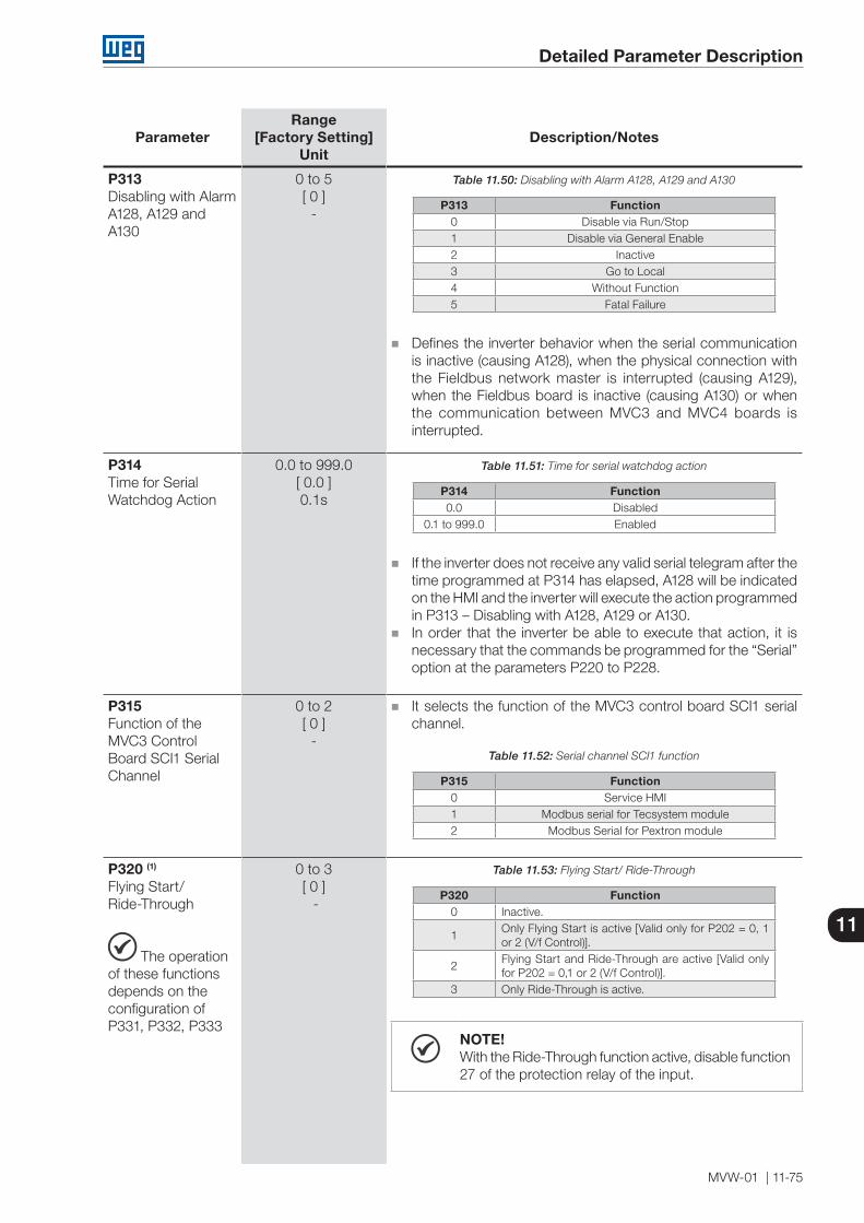
Detailed Parameter Description
MVW-01 | 11-75
11
ParameterRange
[Factory Setting]Unit
Description/Notes
P313Disabling with Alarm A128, A129 and A130
0 to 5[ 0 ]
-
Table 11.50: Disabling with Alarm A128, A129 and A130
P313 Function0 Disable via Run/Stop1 Disable via General Enable2 Inactive3 Go to Local4 Without Function5 Fatal Failure
Defines the inverter behavior when the serial communication is inactive (causing A128), when the physical connection with the Fieldbus network master is interrupted (causing A129), when the Fieldbus board is inactive (causing A130) or when the communication between MVC3 and MVC4 boards is interrupted.
P314Time for SerialWatchdog Action
0.0 to 999.0[ 0.0 ]0.1s
Table 11.51: Time for serial watchdog action
P314 Function0.0 Disabled
0.1 to 999.0 Enabled
If the inverter does not receive any valid serial telegram after the time programmed at P314 has elapsed, A128 will be indicated on the HMI and the inverter will execute the action programmed in P313 – Disabling with A128, A129 or A130.
In order that the inverter be able to execute that action, it is necessary that the commands be programmed for the “Serial” option at the parameters P220 to P228.
P315Function of theMVC3 ControlBoard SCI1 SerialChannel
0 to 2[ 0 ]
-
It selects the function of the MVC3 control board SCI1 serial channel.
Table 11.52: Serial channel SCI1 function
P315 Function0 Service HMI1 Modbus serial for Tecsystem module2 Modbus Serial for Pextron module
P320 (1) Flying Start/Ride-Through
The operation of these functions depends on the configuration of P331, P332, P333
0 to 3[ 0 ] -
Table 11.53: Flying Start/ Ride-Through
P320 Function0 Inactive.
1Only Flying Start is active [Valid only for P202 = 0, 1 or 2 (V/f Control)].
2Flying Start and Ride-Through are active [Valid only for P202 = 0,1 or 2 (V/f Control)].
3 Only Ride-Through is active.
NOTE!With the Ride-Through function active, disable function 27 of the protection relay of the input.
Detailed Parameter Description
11-76 | MVW-01
11
ParameterRange
[Factory Setting]Unit
Description/Notes
P321 (4)
Ud Line Loss Level
Thisparameter is onlyvisible on thedisplay whenP202 = 3 or 4(Vector Control)
166 V to 800 V(P296 = 0)
252 V1 V
287 V to 800 V(P296 = 1)
436 V1 V
2000 V to 8000 V(P296 = 2)
2681 V1 V
2000 V to 8000 V(P296 = 3)
3847 V1 V
2000 V to 8000 V(P296 = 4)
4850 V1 V
2000 V to 8000 V(P296 = 5)
4644 V1 V
2000 V to 8000 V(P296 = 6)
5363 V1 V
The occurrence of the Ride-Through function can be visualized at the outputs DO1, DO2, RL1, RL2 and/or RL3 (P275, P276, P277, P279 and/or P280) if they have been programmed as “23 = Ride-Through”.
For inverters of rated voltage of 6000 V, 6300 V and 6600 V you must set P296 = 5; however for those values of rated voltage, P321 must be manually set to:6000 V - 4038 V6300 V - 4240 V6600 V - 4442 V
NOTE!When either Ride-Through, is activated, the parameter P214 (Line Phase Loss Detection) is automatically set to 0 = Inactive.
NOTE!Ud = Vac x 1.35.
Ride-Through Vector Control (P202 = 3 or 4): The purpose of the Ride-Through function in vector mode
(P202 = 3 or 4) is to assure that the inverter keeps the motor running without interruption or fault storage during a power failure. The energy necessary to maintain the inverter operation is obtained from the motor/load kinetic energy (inertia) through its controlled deceleration. After the recovery of the line, the motor accelerates again to the speed reference value.
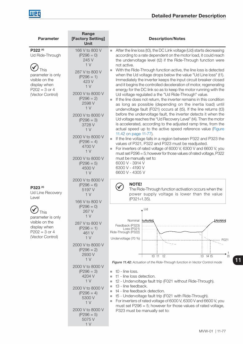
Detailed Parameter Description
MVW-01 | 11-77
11
ParameterRange
[Factory Setting]Unit
Description/Notes
P322 (4)
Ud Ride-Through
Thisparameter is onlyvisible on thedisplay whenP202 = 3 or 4(Vector Control)
P323 (4)
Ud Line RecoveryLevel
Thisparameter is onlyvisible on thedisplay whenP202 = 3 or 4(Vector Control)
166 V to 800 V(P296 = 0)
245 V1 V
287 V to 800 V(P296 = 1)
423 V1 V
2000 V to 8000 V(P296 = 2)
2598 V1 V
2000 V to 8000 V(P296 = 3)
3728 V1 V
2000 V to 8000 V(P296 = 4)
4700 V1 V
2000 V to 8000 V(P296 = 5)
4500 V1 V
2000 V to 8000 V(P296 = 6)
5197 V1 V
166 V to 800 V(P296 = 0)
267 V1 V
287 V to 800 V(P296 = 1)
461 V1 V
2000 V to 8000 V(P296 = 2)
2930 V1 V
2000 V to 8000 V(P296 = 3)
4204 V1 V
2000 V to 8000 V(P296 = 4)
5300 V1 V
2000 V to 8000 V(P296 = 5)
5075 V1 V
After the line loss (t0), the DC Link voltage (Ud) starts decreasing according to a rate dependent on the motor load, it could reach the undervoltage level (t2) if the Ride-Through function were not active.
With the Ride-Through function active, the line loss is detected when the Ud voltage drops below the value "Ud Line loss" (t1). Immediately the inverter keeps the input circuit breaker closed and it begins the controlled deceleration of motor, regenerating energy for the DC link so as to keep the motor running with the Ud voltage regulated a the "Ud Ride-Through" value.
If the line does not return, the inverter remains in this condition as long as possible (depending on the inertia load) until undervoltage fault (F021) occurs at (t5). If the line returns (t3) before the undervoltage fault, the inverter detects it when the Ud voltage reaches the “Ud Recovery Level” (t4). Then the motor is accelerated, according to the adjusted ramp time, from the actual speed up to the active speed reference value (Figure 11.42 on page 11-77).
If the line voltage falls in a region between P322 and P323 the values of P321, P322 and P323 must be readjusted.
For inverters of rated voltage of 6000 V, 6300 V and 6600 V, you must set P296 = 5; however for those values of rated voltage, P322 must be manually set to:6000 V - 3914 V6300 V - 4190 V6600 V - 4305 V
NOTE!The Ride-Through function activation occurs when thepower supply voltage is lower than the value (P321÷1.35).
Feedback (P323)Loss (P321)
Ride-Through (P322)
Ud
F021
t0 t1 t2 t3 t4 t5t(t)
Nominal
Undervoltage (70 %)
Figure 11.42: Actuation of the Ride-Through function in Vector Control mode
t0 - line loss. t1 - line loss detection. t2 - Undervoltage fault trip (F021 without Ride-Through). t3 - line feedback. t4 - line feedback detection. t5 - Undervoltage fault trip (F021 with Ride-Through). For inverters of rated voltage of 6000 V, 6300 V and 6600 V, you
must set P296 = 5; however for those values of rated voltage, P323 must be manually set to:
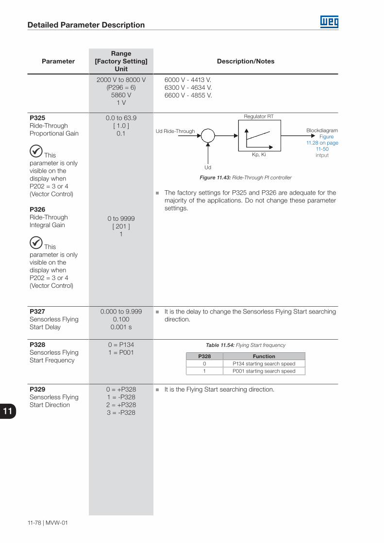
Detailed Parameter Description
11-78 | MVW-01
11
ParameterRange
[Factory Setting]Unit
Description/Notes
2000 V to 8000 V(P296 = 6)
5860 V1 V
6000 V - 4413 V.6300 V - 4634 V.6600 V - 4855 V.
P325Ride-ThroughProportional Gain
Thisparameter is onlyvisible on thedisplay whenP202 = 3 or 4(Vector Control)
P326Ride-ThroughIntegral Gain
Thisparameter is onlyvisible on thedisplay whenP202 = 3 or 4(Vector Control)
0.0 to 63.9[ 1.0 ]0.1
0 to 9999[ 201 ]
1
Ud
Ud Ride-Through Blockdiagram Figure
11.28 on page 11-50 intput
Regulator RT
Kp, Ki
Figure 11.43: Ride-Through PI controller
The factory settings for P325 and P326 are adequate for the majority of the applications. Do not change these parameter settings.
P327Sensorless FlyingStart Delay
0.000 to 9.9990.100
0.001 s
It is the delay to change the Sensorless Flying Start searching direction.
P328Sensorless FlyingStart Frequency
0 = P1341 = P001
Table 11.54: Flying Start frequency
P328 Function0 P134 starting search speed1 P001 starting search speed
P329Sensorless FlyingStart Direction
0 = +P3281 = -P3282 = +P3283 = -P328
It is the Flying Start searching direction.
Detailed Parameter Description
MVW-01 | 11-79
11
ParameterRange
[Factory Setting]Unit
Description/Notes
P331Voltage Ramp
P332Dead Time
P333Ride-Through Time
The parameter P331 is only visible on the display if P202 = 0, 1 or 2 (V/F control)
0.2 to 50.0[ 8.0 ]0.1 s
0.1 to 20.0[ 10.0 ]0.1 s
0.0 to 20.0[ 10.0 ]0.1 s
Parameters are active with P202 = 0, 1 or 2 (V/F Control): Parameter P331 sets the time required for the output voltage,
starting from 0 V, to reach the nominal voltage. The Flying Start function allows starting a spinning motor. This
function only acts when the inverter is enabled, then it imposes the speed of the reference and applies a voltage ramp with the time defined in P331.
The parameter P332 sets the minimum time the inverter waits before restarting the motor after the line recovery in Ride-Through. This time is counted from the line voltage drop, and it is necessary for the motor de-magnetizing. P332 is also used in the start with Flying Start, before the beginning of the Flying Start. Set this time (P332) to twice the rotor constant of the motor
The Ride-Through function allows the inverter recovery without F021 (DC link undervoltage), when a voltage dip occurs in the supply line.
The inverter will indicate F003 (Input transformer secondary undervoltage fault) if the voltage dip lasts longer than P332 + P333 seconds.
If Ride-Through is enabled and a voltage dip occurs, causing the DC link to drop below the undervoltage level, the output pulses are disabled and the motor coasts. If the line supply returns to its normal value, the inverter enables the pulses again, imposing the speed of the reference instantaneously and applying a voltage ramp with the time defined in P331. Refer to the Figure 11.44 on page 11-80. The Flying Start function does not work when P202 = 3 or 4.
During the Ride-Through, the input circuit breaker is opened and the pre-charge relay is activated.
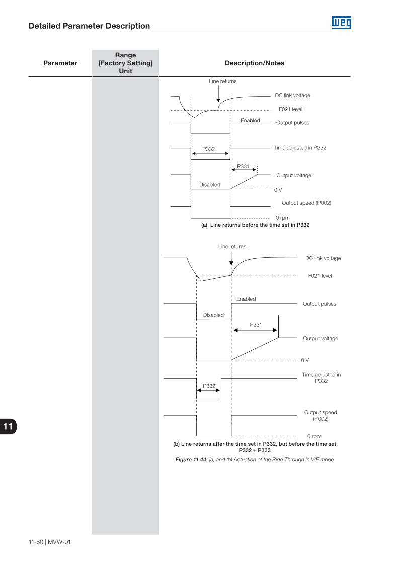
Detailed Parameter Description
11-80 | MVW-01
11
ParameterRange
[Factory Setting]Unit
Description/Notes
Line returns
DC link voltage
F021 level
Enabled
Disabled
Output pulses
Time adjusted in P332P332
P331
Output voltage
0 V
Output speed (P002)
0 rpm (a) Line returns before the time set in P332
Line returns
DC link voltage
F021 level
Output pulsesEnabled
Disabled
P331
Output voltage
Time adjusted in P332
0 V
Output speed (P002)
0 rpm
P332
(b) Line returns after the time set in P332, but before the time set P332 + P333
Figure 11.44: (a) and (b) Actuation of the Ride-Through in V/F mode
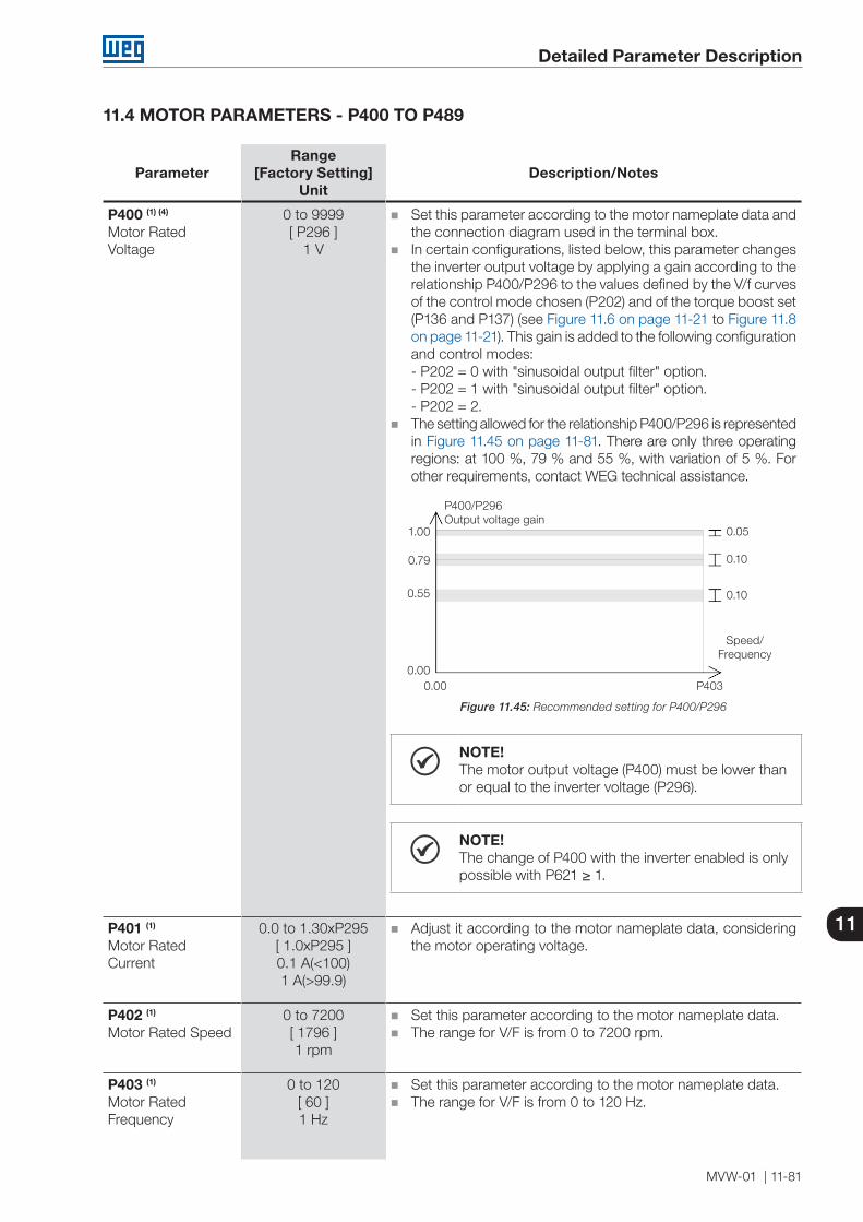
Detailed Parameter Description
MVW-01 | 11-81
11
11.4 MOTOR PARAMETERS - P400 TO P489
ParameterRange
[Factory Setting]Unit
Description/Notes
P400 (1) (4)
Motor RatedVoltage
0 to 9999[ P296 ]
1 V
Set this parameter according to the motor nameplate data and the connection diagram used in the terminal box.
In certain configurations, listed below, this parameter changes the inverter output voltage by applying a gain according to the relationship P400/P296 to the values defined by the V/f curves of the control mode chosen (P202) and of the torque boost set (P136 and P137) (see Figure 11.6 on page 11-21 to Figure 11.8 on page 11-21). This gain is added to the following configuration and control modes:- P202 = 0 with "sinusoidal output filter" option.- P202 = 1 with "sinusoidal output filter" option.- P202 = 2.
The setting allowed for the relationship P400/P296 is represented in Figure 11.45 on page 11-81. There are only three operating regions: at 100 %, 79 % and 55 %, with variation of 5 %. For other requirements, contact WEG technical assistance.
P4030.000.00
1.00
0.55
0.05
0.10
0.10
0.79
Speed/Frequency
P400/P296 Output voltage gain
Figure 11.45: Recommended setting for P400/P296
NOTE!The motor output voltage (P400) must be lower thanor equal to the inverter voltage (P296).
NOTE!The change of P400 with the inverter enabled is onlypossible with P621 ≥ 1.
P401 (1) Motor RatedCurrent
0.0 to 1.30xP295[ 1.0xP295 ]0.1 A(<100) 1 A(>99.9)
Adjust it according to the motor nameplate data, considering the motor operating voltage.
P402 (1) Motor Rated Speed
0 to 7200[ 1796 ]1 rpm
Set this parameter according to the motor nameplate data. The range for V/F is from 0 to 7200 rpm.
P403 (1) Motor RatedFrequency
0 to 120[ 60 ]1 Hz
Set this parameter according to the motor nameplate data. The range for V/F is from 0 to 120 Hz.
Detailed Parameter Description
11-82 | MVW-01
11
ParameterRange
[Factory Setting]Unit
Description/Notes
P405Encoder Data
100 to 9999[ 1024 ]
ppr
Program the number of pulses per revolution (PPR) of the used incremental encoder when P202 = 4 (Vector with Encoder).
P406 (1) (2)
Motor Ventilation0 or 1[ 0 ]
-
Table 11.55: Type of motor ventilation
P406 Motor Ventilation0 Self-ventilated1 Separated ventilation
In the first power-up (refer to Chapter 8 INSTALLATION, CONNECTION AND ENERGIZATION on page 8-1) the value set in P406 automatically modifies the overload protection according to the description of parameters P156, P157 and P158.
P408 (1)
Self-Tuning0 or 1[ 0 ]
-
With P408 = 1 (Autogain) the gains of the vector control regulators are automatically recalculated when the motor configuration parameters are changed.
Table 11.56: Self-Tuning
P408 Function0 No autogain1 Autogain
P409 (1)
Motor StatorResistance (Rs)
0.000 to 9.999[ 0.000 ]0.001 Ω
It is the value of the motor stator resistance.
P410MotorMagnetizationCurrent (Imr)
0 to 1.25xP295[ 0.0 ]0.1 A
It is the value of the motor magnetization current.
P411 (1)
Motor Flux LeakageInductance (Is)
0.00 to 99.99[ 0.00 ]
0.01 mH
It is the value of the motor flux leakage inductance.
P412 (1)
Lr/Rr Constant(Rotor TimeConstant-Tr)
0.000 to 9.999[ 0.000 ]0.001 s
Typical Tr values for standard WEG motors.
P413 (1) TM Constant(Mechanical TimeConstant)
0.00 to 99.99[ 0.00 ]0.01 s
It is the mechanical time constant of the driven load.

Detailed Parameter Description
MVW-01 | 11-83
11
ParameterRange
[Factory Setting]Unit
Description/Notes
P414MagnetizingVoltage
This parameteris only visible whenP202 = 0, 1 or 2(V/F control)
0.0 to 20.0[ 0.0 ]0.1 %
It is a percentage of the nominal voltage applied during 2 x P412 to magnetize the motor when starting it.
11.5 PARAMETERS OF THE SYNCHRONOUS MOTOR - P427 TO P465
NOTE!Parameters of the Synchronous Motor only visible with P950 = 1 (Synchronous Motor).
ParameterRange
[Factory Setting]Unit
Description/Notes
P427Inductance LDσ
0.00 to 99.99[ 4.85 ]1 mH
Motor parameter used on the stator flux observer.
Complete stator fluxobserver
P427, P428, P429, P430, P431, P433, P434, P436 and P437
id, iq
θ
md, mq,
Stator model +
saturation curveΦ
Figure 11.46: Complete model of the stator flow
ud
uf
Rf
RDRS
if
imd
id Lσd
Lmdωψsq
LσD
Lσf
iQ
uq
RQRS
imq
iq Lσq
Lmq-ωψsd
LσQ iD
Figure 11.47: Electrical model of a synchronous motor
P428Inductance LQσ
0.00 to 99.99[ 4.41 ]1 mH
Motor parameter used in stator flux model.
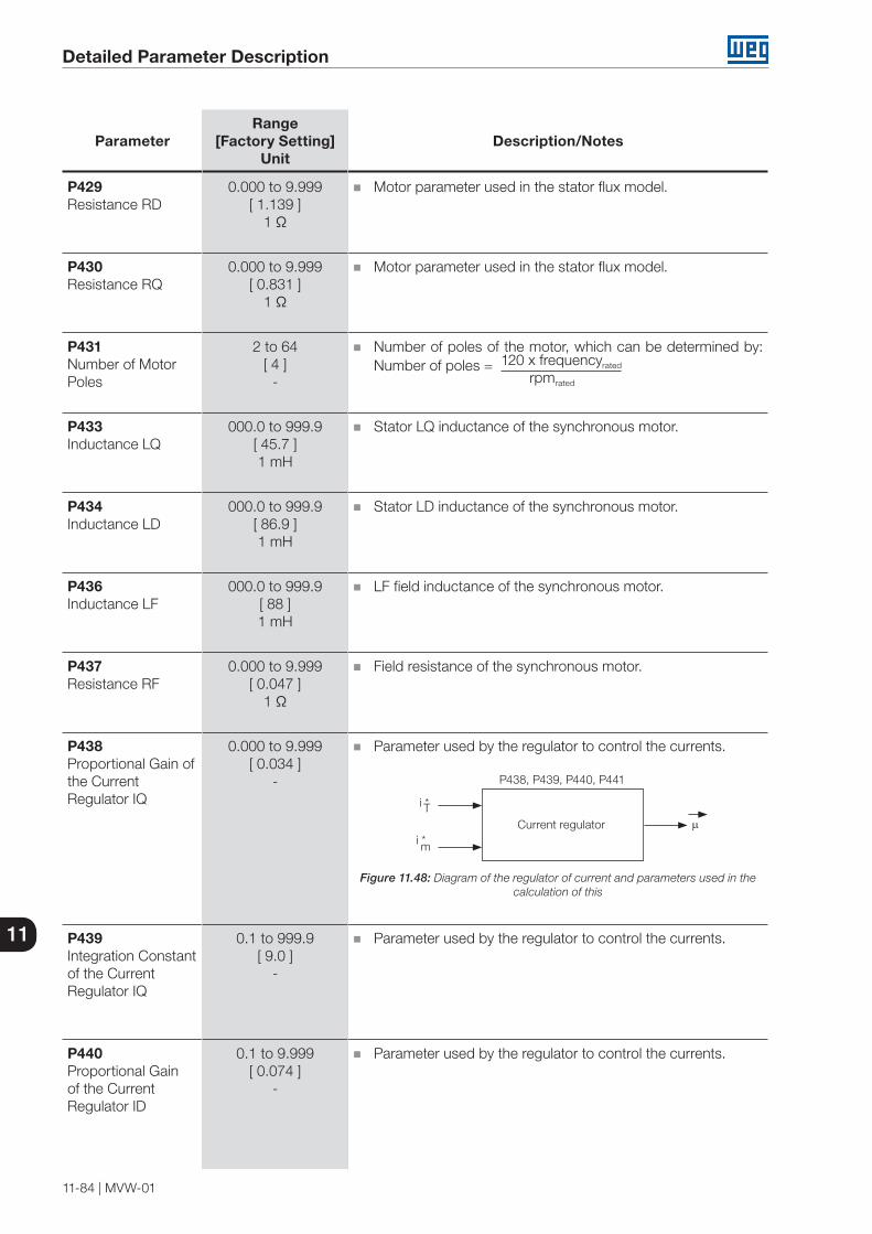
Detailed Parameter Description
11-84 | MVW-01
11
ParameterRange
[Factory Setting]Unit
Description/Notes
P429Resistance RD
0.000 to 9.999[ 1.139 ]
1 Ω
Motor parameter used in the stator flux model.
P430Resistance RQ
0.000 to 9.999[ 0.831 ]
1 Ω
Motor parameter used in the stator flux model.
P431Number of Motor Poles
2 to 64[ 4 ]
-
Number of poles of the motor, which can be determined by: Number of poles = 120 x frequencyrated
rpmrated
P433Inductance LQ
000.0 to 999.9[ 45.7 ]1 mH
Stator LQ inductance of the synchronous motor.
P434Inductance LD
000.0 to 999.9[ 86.9 ]1 mH
Stator LD inductance of the synchronous motor.
P436Inductance LF
000.0 to 999.9[ 88 ]1 mH
LF field inductance of the synchronous motor.
P437Resistance RF
0.000 to 9.999[ 0.047 ]
1 Ω
Field resistance of the synchronous motor.
P438Proportional Gain ofthe Current Regulator IQ
0.000 to 9.999[ 0.034 ]
-
Parameter used by the regulator to control the currents.
P438, P439, P440, P441
Current regulator
i *T
i *m
m
Figure 11.48: Diagram of the regulator of current and parameters used in the calculation of this
P439Integration Constant of the Current Regulator IQ
0.1 to 999.9[ 9.0 ]
-
Parameter used by the regulator to control the currents.
P440Proportional Gain of the Current Regulator ID
0.1 to 9.999[ 0.074 ]
-
Parameter used by the regulator to control the currents.

Detailed Parameter Description
MVW-01 | 11-85
11
ParameterRange
[Factory Setting]Unit
Description/Notes
P441IntegrationConstant of the IDCurrent Regulator
0.1 to 999.9[ 19.6 ]
-
Parameter used by the regulator to control the currents.
P442Proportional Gain ofthe Field CurrentRegulator
0.000 to 9.999[ 0.788 ]
-
Function not implemented in this software version.
P443IntegrationConstant of theField CurrentRegulator
0.1 to 999.9[ 703 ]
-
Function not implemented in this software version.
P444Maximum FieldVoltage (Brushless)
0.01 to 1.00[ 0.58 ]
PU
Function not implemented in this software version.
P445Minimum FieldVoltage (Brushless)
0.01 to 1.00[ 0.01 ]
PU
Function not implemented in this software version.
P446Base Field Current
0.1 to 999.9[ 33.3 ]
1 A
Current base used for the field current.
P447ProportionalGain of theField Regulator
0.000 to 9.999[ 0.087 ]
-
PI (integrator proportional) gain used in the reference of the field regulator.
P448IntegrationConstant ofthe FieldRegulator
1 to 9999[ 70 ]
-
PI (integrator proportional) gain used in the reference of the field regulator.
P449Maximum FieldCurrent (Brushless)
0.01 to 5.00[ 0.7 ] PU
Maximum limit in PU of P462 used in the control of the field current reference; see Section 7.2 FIELD EXCITATION SET (DC WITH BRUSHES) on page 7-3. Set according to the possible overload on the inverter/exciter.
P450Minimum FieldCurrent (Brushless)
0.01 to 5.00[ 0.01 ]
PU
Minimum limit in PU of P462 used in the control of the field current reference; see Section 7.2 FIELD EXCITATION SET (DC WITH BRUSHES) on page 7-3.
Minimum field for frequency higher than P452.
Detailed Parameter Description
11-86 | MVW-01
11
ParameterRange
[Factory Setting]Unit
Description/Notes
P451Minimum Field forSoft-Start Function
0.01 to 5.00[ 0.15 ]
PU
Minimum field in PU of P462 used in the control of the field current reference (see Section 7.2 FIELD EXCITATION SET (DC WITH BRUSHES) on page 7-3).
Minimum field for frequency lower than or equal to P452. Used in the soft-start function without rotor orientation in scalar
mode.
NOTE!Function used in motor without encoder.
P452Field InputFrequency
0.00 to 10.00[ 0 ] Hz
Input frequency of the field excitation in scalar mode used in the soft-start function without rotor orientation.
NOTE!In scalar mode without encoder, the motor must ‘‘match’’ the inverter, and it is not possible the start ofmotors of currents higher than the inverter current.
NOTE!When encoder is used, this parameter must be set to0 Hz, disabling the soft-start without encoder function.
ATTENTION!For encoder setting:- Set parameter P452 (field input frequency) equal to0 Hz.- The control type (P202) must be scalar and the direction of rotation forward; configure one of the analog outputs for the encoder setting (E.g.: P656 =[018] EncAdjMS).
NOTE!For further information, contact WEG Technical Assistance.
P453Field Ramp Time
0.00 to 30.00[ 1 ]
0.01 s
Field ramp time in seconds, used in the field regulator reference. Used in the field soft-start.

Detailed Parameter Description
MVW-01 | 11-87
11
ParameterRange
[Factory Setting]Unit
Description/Notes
P454Polynomial A1 ofthe MagneticSaturation Curve
0.000 to 9.999[ 0.000 ]
-
Coefficient of the polynomial of the magnetic saturation curve. The machine operates with linear flux up to the point in which
the linear curve follows the saturation curve; from this point the machine flux follows a mathematical model obtained from the data of the motor manufacturer.
Field current (A)0 10 20155
0
1
2
3
4
0.5
1.5
2.5
3.5
Flux
(PU
)Mathematical approximationSaturation curve
Magnetic saturation curve
Linear curve
Figure 11.49: Typical saturation curve and mathematical approximations used by the inverter for flux control
NOTE!For further information, contact WEG Technical Assistance.
P455Polynomial B1 ofthe MagneticSaturation Curve
0.000 to 9.999[ 0.174 ]
-
Coefficient of the polynomial of the magnetic saturation curve.
P456Polynomial C1 ofthe Magnetic Saturation Curve
0.000 to 9.999[ 1.059 ]
-
Coefficient of the polynomial of the magnetic saturation curve.
P457Polynomial A2 ofthe Gain Curve ofthe BrushlessExciter
0.000 to 9.999[ 0.185 ]
-
Function not implemented in this software version.
P458Polynomial B2 ofthe Gain Curve ofthe BrushlessExciter
0.000 to 9.999[ 0.068 ]
-
Function not implemented in this software version.
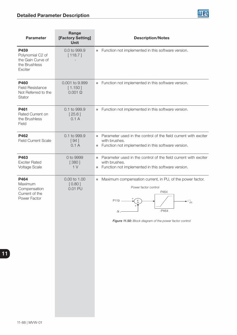
Detailed Parameter Description
11-88 | MVW-01
11
ParameterRange
[Factory Setting]Unit
Description/Notes
P459Polynomial C2 ofthe Gain Curve ofthe Brushless Exciter
0.0 to 999.9[ 118.7 ]
-
Function not implemented in this software version.
P460Field ResistanceNot Referred to theStator
0.001 to 9.999[ 1.150 ] 0.001 Ω
Function not implemented in this software version.
P461Rated Current onthe BrushlessField
0.1 to 999.9[ 25.6 ] 0.1 A
Function not implemented in this software version.
P462Field Current Scale
0.1 to 999.9[ 94 ] 0.1 A
Parameter used in the control of the field current with exciter with brushes.
Function not implemented in this software version.
P463Exciter RatedVoltage Scale
0 to 9999[ 380 ] 1 V
Parameter used in the control of the field current with exciter with brushes.
Function not implemented in this software version.
P464MaximumCompensationCurrent of thePower Factor
0.00 to 1.00[ 0.80 ]
0.01 PU
Maximum compensation current, in PU, of the power factor.
Power factor controlP464
∑+
+i m*P119
∆i f-P464
Figure 11.50: Block diagram of the power factor control
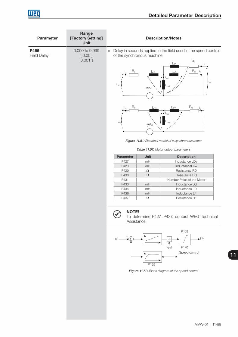
Detailed Parameter Description
MVW-01 | 11-89
11
ParameterRange
[Factory Setting]Unit
Description/Notes
P465Field Delay
0.000 to 9.999[ 0.00 ] 0.001 s
Delay in seconds applied to the field used in the speed control of the synchronous machine.
ud
uf
Rf
RDRS
if
imd
id Lσd
Lmdωψsq
LσD
Lσf
iQ
uq
RQRS
imq
iq Lσq
Lmq-ωψsd
LσQ iD
Figure 11.51: Electrical model of a synchronous motor
Table 11.57: Motor output parameters
Parameter Unit DescriptionP427 mH Inductance LDσP428 mH InductanceLQσP429 W Resistance RDP430 W Resistance RQP431 Number Poles of the MotorP433 mH Inductance LQP434 mH Inductance LDP436 mH Inductance LFP437 W Resistance RF
NOTE!To determine P427...P437, contact WEG Technical Assistance
Speed control
P169
P165
P170lψsl
∑+
-i T*ω*
ω
Figure 11.52: Block diagram of the speed control

Detailed Parameter Description
11-90 | MVW-01
11
11.6 PARAMETER OF THE GRAPHIC HMI - P490 TO P519
ParameterRange
[Factory Setting]Unit
Description / Notes
P490Graphic HMI LCDContrastAdjustment
0 to 150[ 80 ]
%
It adjusts the Graphic LCD contrast percentage.
P491Graphic HMIConfiguration
0 to 2[ 0 ] -
It configures the origin of the inverter Local or Remote (LOC/REM) commands for the ‘Serial’ type, so that the Graphic HMI be able to operate in an adequate manner (the Graphic HMI commands are of the Modbus RTU serial type).
Table 11.58: Graphic HMI commands selection
P491 Function
0 Inactive
1 Local HMIG2 Remote HMIG
P493Sampling Timeof the On-lineGraphic Function
1 to 100[ 10 ]
1 x 10 ms
It adjusts the time between the points presented in the On-line Graphic Function.
P500Read-onlyParameter #1Selection
P501Read-onlyParameter #2Selection
P502Read-onlyParameter #3Selection
P503Read-onlyParameter #4Selection
P504Read-onlyParameter #5Selection
P505Read-onlyParameter #6Selection
0 to 9[ 0 ] 2
0 to 9[ 0 ] 0
0 to 9[ 0 ] 0
0 to 9[ 0 ] 0
0 to 9[ 0 ] 0
0 to 9[ 0 ] 0
It selects one of the monitoring parameters. From 1 to 6 read-only parameters can be programmed for simultaneous exhibition among the 9 available ones.
Table 11.59: Read-only parameters selection
P500...P505 Read-only Parameter0 Inactive1 P0012 P0023 P0034 P0045 P0056 P0077 P0098 P0109 P040

Detailed Parameter Description
MVW-01 | 11-91
11
ParameterRange
[Factory Setting]Unit
Description / Notes
P512On-line GraphicFunctionParameter #1Selection
P513On-line GraphicFunctionParameter #2Selection
0 to 9[ 0 ] 2
0 to 9[ 0 ] 3
It selects one of the parameters to be monitored by the On-line Graphic Function (Watch Function).
Table 11.60: On-line graphic function parameters selection
P512...P513 Read-only Parameter0 Inactive1 P0012 P0023 P0034 P0045 P0056 P0077 P0098 P0109 P040
P516Full Scale ofthe On-lineGraphic FunctionParameter #1
P517Full Scale ofthe On-lineGraphic FunctionParameter #2
0 to 200[ 100 ]
%
0 to 200[ 100 ]
%
It adjusts the full scale of the on-line graphic correspondent parameter.
Table 11.61: Adjust of the full scale of the on-line graphic function
P516...P517 Full ScaleP001 P208P002 P208P003 P295P004 1.35 x P296P005 P403P007 P296P009 (P295 / P401) x 100 %P010 1.732 x (P295 x P296)P040 100 %
Detailed Parameter Description
11-92 | MVW-01
11
11.7 PARAMETERS OF THE PID FUNCTION - P520 TO P535
ParameterRange
[Factory Setting]Unit
Description/Notes
P520PID ProportionalGain
P521PID Integral Gain
P522PID Differential Gain
P523PID Ramp Time
Theseparameters areonly visible on thedisplay if P203 = 1or 3
0.000 to 7.999[ 1.000 ]0.001
0.000 to 9.999[ 1.000 ]
0.001 (<9.999)0.01 (>9.999)
0.000 to 9.999[ 0.000 ]0.001
0.0 to 999.0[ 3.0 ]
0.1s (<99.9s)1s (>99.9s)
The initial gain and PID ramp settings recommendation for some applications mentioned in the Section 12.2 PID Regulator on page 12-6, are given in the Table 11.62 on page 11-92.
Table 11.62: PID initial gain setting suggestions
GainsP523PID
Ramp
P527Actiontype
Process variable Proportional Integral Proportional
P520 P521 P522
Pneumatic system
pressure1 0.043 0.000 3 0 = Direct
Pneumatic system flow
1 0.037 0.000 3 0 = Direta
Hydraulic system
pressure1 0.043 0.000 3 0 = Direct
Hydraulic system flow
1 0.037 0.000 3 0 = Direct
Temperature 2 0.004 0.000 3 NotesLevel 1 Notes 0.000 3 Notes
Notes:- For temperature and level, the action type setting will depend
on the process. For level control, for instance, if the inverter drives the motor that pumps fluid out of the reservoir, the action will be reverse because when the level increases the inverter must increase the motor speed in order to lower the level, otherwise, when the inverter drives a motor that pumps fluid into the reservoir, the action will be direct..
- In case of level control, the integral gain adjustment will depend on the time required for the reservoir to pass from the minimum acceptable to the desired level, in the following conditions:
I. For direct action, the time must be measured with maximum input flow and minimum output flow.
II. For reverse action, the time must be measured with minimum input flow and maximum output flow.
An equation to calculate an initial value for P521 (PID IntegralGain) as a function of the system response time, is presentedbelow:
P521 = 0.02 / tt = time (seconds)

Detailed Parameter Description
MVW-01 | 11-93
11
ParameterRange
[Factory Setting]Unit
Description/Notes
P524 (1)
PID FeedbackSelection
Thisparameter is onlyvisible on thedisplay if P203 = 1or 3
0 or 1[ 0 ]
-
It defines the PID regulator feedback (Process variable) input.
Table 11.63: Feedback input selection
P524 AIx0 AI2 (P237 to P240 and P248)1 AI3 (P241 to P244)
After the feedback input has been chosen, the function of the selected input must be programmed at P237 (for AI2) or at P241 (for AI3).
Feedback type:- The PID action type described above considers that the
process variable feedback signal increases when the process variable also increases (direct feedback). This is the most used feedback type.
- If the process variable feedback decreases as the process variable increases (inverse feedback), then it is necessary to program the selected PID feedback analog input as inverse reference: For AI2 feedback, P239 = 2 (10 to 0 V/20 to 0 mA) or P239 = 3 (20 to 4 mA). For AI3 feedback, P243 = 2 (10 to 0 V/20 to 0 mA) or P243 = 3 (20 to 4 mA). Without this setting, the PID does not operate correctly.
P525Keypad PID Setpoint and
This parameter is only visible on thedisplay if P203 = 1or 3
0.0 to 100.0[ 0.0 ]0.1 %
It provides the PID regulator setpoint that is adjusted via the and keys provided that P221 = 0 (Local) or P222 = 0
(Remote), and in automatic mode. If the PID is in manual mode, then the speed reference is given by P121.
When the PID regulator is operating in automatic mode, the setpoint is the one defined as speed reference via P221 (Local) or P222 (Remote). The majority of PID applications either use setpoint via analog input AI1 (P221 = 1 in Local, or P222 = 1 in Remote), or via and keys (P221 = 0 in Local, or P222 = 0 in Remote). Refer to the Figure 12.6 on page 12-8.
P526Process VariableFilter
Thisparameter is onlyvisible on thedisplay if P203 = 1or 3
0.0 to 16.0[ 0.1 ]0.1 s
It adjusts the process variable filter time constant. The 0.1 s value is usually adequate, unless the process variable
presents much noise. In such case, increase the value gradually, observing the result.

Detailed Parameter Description
11-94 | MVW-01
11
ParameterRange
[Factory Setting]Unit
Description/Notes
P527PID Action Type
Thisparameter is onlyvisible on thedisplay if P203 = 1or 3
0 or 1[ 0 ]
-
It defines the type of PID control action:
Table 11.64: PID action type
P527 Action type0 Direct1 Reverse
Selection criteria:
Table 11.65: Selection of operation
Motor speed Process variable Action type
IncreasesIncreases DirectDecreases Reverse
Selection according to the process requirements:- PID action type: the action must be selected as Direct when
it is necessary to increase the motor speed to increase the process variable. Otherwise, select Reverse.
Example 1 – Direct: the inverter drives a pump responsible forfilling a water reservoir using the PID to control the level. In orderthat the level (process variable) increases, it is necessary that theflow, and consequently the motor speed, also increases.Example 2 – Reverse: The inverter drives a fan responsible for refrigerating a cooling tower using the PID to control the temperature. In order to increase the temperature (process variable), it is necessary to decrease the ventilation by decreasing the motor speed.
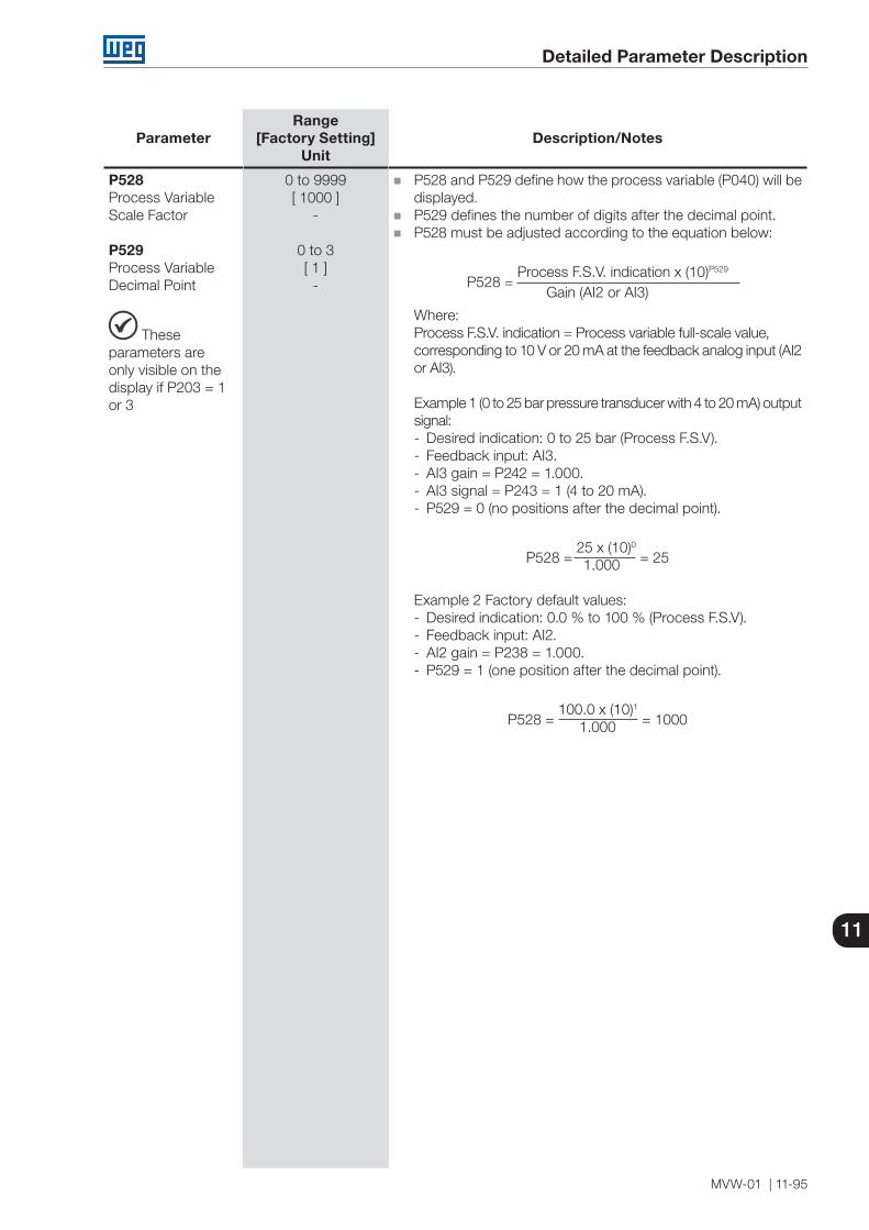
Detailed Parameter Description
MVW-01 | 11-95
11
ParameterRange
[Factory Setting]Unit
Description/Notes
P528Process VariableScale Factor
P529Process VariableDecimal Point
Theseparameters areonly visible on thedisplay if P203 = 1or 3
0 to 9999[ 1000 ]
-
0 to 3[ 1 ]
-
P528 and P529 define how the process variable (P040) will be displayed.
P529 defines the number of digits after the decimal point. P528 must be adjusted according to the equation below:
P528 = Process F.S.V. indication x (10)P529
Gain (AI2 or AI3)
Where:Process F.S.V. indication = Process variable full-scale value,corresponding to 10 V or 20 mA at the feedback analog input (AI2or AI3).
Example 1 (0 to 25 bar pressure transducer with 4 to 20 mA) outputsignal:- Desired indication: 0 to 25 bar (Process F.S.V).- Feedback input: AI3.- AI3 gain = P242 = 1.000.- AI3 signal = P243 = 1 (4 to 20 mA).- P529 = 0 (no positions after the decimal point).
P528 = 25 x (10)0
= 25 1.000
Example 2 Factory default values:- Desired indication: 0.0 % to 100 % (Process F.S.V).- Feedback input: AI2.- AI2 gain = P238 = 1.000.- P529 = 1 (one position after the decimal point).
P528 = 100.0 x (10)1
= 10001.000
Detailed Parameter Description
11-96 | MVW-01
11
ParameterRange
[Factory Setting]Unit
Description/Notes
P530Process VariableEngineering Unit 1
P531Process VariableEngineering Unit 2
P532Process VariableEngineering Unit 3
Theseparameters areonly visible on thedisplay if P203 = 1or 3
32 to 127[ 37 ( % ) ]
-
32 to 127[ 32 ( ) ]
-
32 to 127[ 32 ( ) ]
-
These parameters are useful only for inverters fitted with an LCD keypad.
The process variable engineering unit is formed by three characters, which will be applied to the parameter P040 indication. P530 defines the leftmost character, P531 the center one and P532 the rightmost.
Characters that can be chosen:Characters corresponding to ASCII code from 32 to 127.Examples:A, B, ... , Y, Z, a, b, ... , y, z, 0, 1, ... , 9, #, $, %, (, ), *, +, ...
Examples:- To indicate "bar":
P530 = "b" (98)P531 = "a" (97)P532 = "r" (114)
- To indicate "%":P530 = "%” (37)P531 = " " (32)P532 = " " (32)
NOTE!The configuration of the engineering unit is only validfor the service HMI.
P533VPx Value
P534VPy Value
P535Output N = 0 PID
Theseparameters areonly visible on thedisplay if P203 = 1or 3
0.0 to 100.0[ 90.0 ]0.1 %
0.0 to 100.0[ 10.0 ]0.1 %
0 to 100[ 0 ]1 %
They are used with the digital and relay output functions:V. Pr. > VPx and V. Pr. < VPy with the function of signal/alarm.
The process variable full scale value in percentage is:
(P040 = (10)P529
x 100 %)P528
P535 works together with P212 (Condition to Leave Zero Speed Disable), giving an additional condition to leave the disabled condition, i.e., PID error > P535. Refer to P211 and P213 descriptions.
11.8 PARAMETERS OF THE TRACE FUNCTION
ParameterRange
[Factory Setting]Unit
Description/Notes
P550Trigger Parameter
0 to 746[ 0 ]
-
Program the number of the parameter to be used as trigger for the Trace function.Example:By programming P550 = 4 the trigger parameter will be P004 (DC Link Voltage).Note: When the trigger is defined by alarm or fault, then P550 can have any value. Refer to the P552 description.

Detailed Parameter Description
MVW-01 | 11-97
11
ParameterRange
[Factory Setting]Unit
Description/Notes
P551Trigger Value
-32768 to +32767[ 0 ]
-
The value programmed in P551 is compared to the contents of the parameter defined at P550. If the trigger condition is fulfilled, (refer to P552), the Trace function will be triggered.
The user must apply the processor internal representation, so that the Trace function works properly.Example:If P550 = 100, set P551 = 100 in case the user wishes to compare P100 (acceleration ramp) with a setting of 10.0 seconds for the trigger.
P552Trigger Condition
0 to 20[ 4 ]
-
Refer to P550. With the factory default programming (refer to the Trace function
programming example, Figure 12.1 on page 12-1) the trigger is defined as a fault trip.
Trigger condition of the trace function, according to the table below.
Table 11.66: Trace function trigger condition
P552 Trigger Condition0 P550* = P5511 P550* ≠ P5512 P550* > P5513 P550* < P551
4 Inverter in state fault
- Binary Selection (bit mask)
Respective DI (P550 = 12)
Respective DO (P550 = 13)
5 P550* bit 0 = P551 DI8 -6 P550* bit 1 = P551 DI7 RL57 P550* bit 2 = P551 DI6 RL48 P550* bit 3 = P551 DI5 RL39 P550* bit 4 = P551 DI4 RL210 P550* bit 5 = P551 DI3 RL111 P550* bit 6 = P551 DI2 DO212 P550* bit 7 = P551 DI1 DO113 P550* bit 8 = P551 DI9 -14 P550* bit 9 = P551 DI10 -15 P550* bit 10 = P551 - -16 P550* bit 11 = P551 - -17 P550* bit 12 = P551 - -18 P550* bit 13 = P551 - -19 P550* bit 14 = P551 - -20 P550* bit 15 = P551 - -
* Contents of the parameter programmed at P550.
Note: the binary selection conditions (5 to 20) are only effectiveif the parameter programmed in P550 is 12 or 13 (P012 or P013).

Detailed Parameter Description
11-98 | MVW-01
11
ParameterRange
[Factory Setting]Unit
Description/Notes
P553Sampling Time
1 to 9999[ 1 ]
x500 μs
It is the trace channels sampling time (as a multiplier of the 500 μs time base).Example:If P553 = 10 (10 x 500 m), a sampling time of 5 ms is obtained.
P554Pre-TriggerPercentage
0 to 100[ 50 ]1 %
It is the percentage of trace data before the trigger event that has to be recorded.
P555CH1 - Tracechannel 1
P557CH2 - Tracechannel 2
P559CH3 - Tracechannel 3
P561CH4 - Tracechannel 4
P563CH5 - Tracechannel 5
P565CH6 - Tracechannel 6
P567CH7 - Tracechannel 7
P569CH8 - Tracechannel 8
0 to 727[ 001 ][ 002 ][ 003 ][ 004 ][ 005 ][ 006 ][ 007 ][ 073 ]
-
Number of the parameter that will be recorded by the Trace function at the respective channel.
The setting 0 means inactive channel. With the factory default settings (refer to the Trace function
programming, Figure 12.1 on page 12-1) the following parameters are programmed with the Trace function:
Table 11.67: Channels of trace
Channel Parameter Description1 P001 Speed Reference2 P002 Motor Speed3 P003 Motor Current4 P004 DC Link Voltage5 P005 Motor Frequency6 P006 Inverter Status7 P007 Output Voltage8 P074 Line voltage
When the channel is configured for P012 (status of the digital inputs) or P013 (status of the digital inputs) see Table 11.68 on page 11-99.

Detailed Parameter Description
MVW-01 | 11-99
11
ParameterRange
[Factory Setting]Unit
Description/Notes
P556CH1 Trace Mask
P558CH2 Trace Mask
P560CH3 Trace Mask
P562CH4 Trace Mask
P564CH5 Trace Mask
P566CH6 Trace Mask
P568CH7 Trace Mask
P570CH8 Trace Mask
0 to 16[ 0 ]
-
They define the record manner of the respective channel during trace acquisition.
Table 11.68: Trace record type
Value Record Type DI DO
0 Normal1 Only the bit 0 DI8 -2 Only the bit 1 DI7 RL53 Only the bit 2 DI6 RL44 Only the bit 3 DI5 RL35 Only the bit 4 DI4 RL26 Only the bit 5 DI3 RL17 Only the bit 6 DI2 DO28 Only the bit 7 DI1 DO19 Only the bit 8 DI9 -10 Only the bit 9 DI10 -11 Only the bit 10 - -12 Only the bit 11 - -13 Only the bit 12 - -14 Only the bit 13 - -15 Only the bit 14 - -16 Only the bit 15 - -

Detailed Parameter Description
11-100 | MVW-01
11
ParameterRange
[Factory Setting]Unit
Description/Notes
P571Trace Activation
0 or 1[ 0 ]
-
It programs the trace function, initiating its operation.
NOTE!The trace programming becomes active when this parameter changes from inactive to active. Thus, if the trace function is active and the trace parameters are reprogrammed, those changes will only go into effect when trace is disabled (P571 = 0) and then enabled again (P571 = 1).
Table 11.69: Trace activation
P571 Trace0 Inactive1 Active
P572Trace MemoryPercentage
1 to 100[ 100 ]
1%
It defines the percentage of the available memory that will be used for the Trace function recording.
When the user wants short time intervals, then values smaller than 100 % could be useful for the visualization at the analog outputs, and in the data transfer to the SuperDrive software.
In order to calculate the memory available for each channel when P572 is different from 100 %, one must simply consider the total memory of each board as:
P572/100 x total board memory
Example:Memory available for each channel = 7.77kword.
Sampling time equal to 500 μs (P553 = 1).
If P572 = 100 %, then: 7770 x 500 ms = 3.885 s record.
If P572 = 10 %, then: 777 x 500 ms = 0.3885 s record, and 90 % of the memory is not used.
If P572 = 1 %, then: 77 x 500 ms = 0.0385 s record, and 90 %of the memory is not used.

Detailed Parameter Description
MVW-01 | 11-101
11
ParameterRange
[Factory Setting]Unit
Description/Notes
P621Sinusoidal Filter
0 to 2[0]-
It enables proper modulation for operation with sinusoidal filter.
Table 11.70: Sinusoidal Filter
P621 Function0 Inactive (OPP)1 Active (SHE)2 Active with current oversample (SHE)
P622Boost FinalFrequency: IxR
0 to 9999[4095]
-
It determines the final actuation frequency of the manual torque boost.
For further information, refer to parameter P136. The frequency is determined by the equation below:
P622 (Hz) = P622 8192
. P403
P629Synchronism Time OK
1 to 20[1]s
Minimum time the inverter must maintain the phase error between the line voltage and the inverter output voltage smaller than the setting in P632 so as to signal it as synchronism OK.
P630Synchronism Timeout
20 to 240[60]
s
Time out of synchronism with the line. Time counted from the activation of the DI of the MVC4, which
starts the search until the signaling of synchronism OK. If this time is exceeded, A008 will be indicated.
P631DI13 Delay
0 to 3000[170]
x500µs
Delay of DI13 of the MVC3 board, used to disable the inverter after the transfer.
This time is used to compensate the delay on the transfer circuit, preventing the motor from remaining for a time interval without voltage.
P632Maximum Phase Error
0 to 9999[1966]
-
Phase error between the line voltage and the inverter voltage used together with P629 to indicate synchronism OK.
(P632 / 65536) x 360º = value in degrees.
P636Phase Adjustment
-32768 to 32767[0]-
Parameter used to compensate the phase error between the voltage the inverter uses as reference for synchronism and the actual voltage in the point where the transfer will occur.
Possible setting between (-180° and +180°). (P636 / 65536) x 360° = value in degrees.

Detailed Parameter Description
11-102 | MVW-01
11
11.9 PARAMETERS OF THE MVC3 ANALOG OUTPUTS - P652 TO P666
Parameter
Range[Factory Setting]
UnitDescription/Notes
P652Fast Analog Output Function AO1 MVC3
0 to 255[ 2 ]
-
Table 11.71: Function of the analog outputs of the MVC3 board
P652, P654, P656 and
P658Function Full Scale
0 Phase Current V 5 V = P2951 Phase Current W 5 V = P2952 Phase Current U 5 V = P2953 Output Frequency 10 V = 120 Hz4 Angle of the Fundamental Output Voltage 10 V = +180º5 Modulation Index 5 V = 255
17Reference of Voltage and Field Current for
Synchronous Machine 10 V = P462 (A)10 V = P463 (V)
18Position Adjustment of the Absolute
Encoder 10 V = +180º
34 Value fixe at 0 V -35 Value fixe at 10 V -36 Value fixe at -10 V -
37Voltage between Phase A and B
Measured on the Line ISOX Board 5 V = VAB
Rated
38Voltage between Phase B and C
Measured on the Line ISOX Board 5 V = VBC
Rated
60 Temperature of Phase U 0 V = -20º
10 V = 200 ºC
61 Temperature of Phase V 0 V = -20º
10 V = 200 ºC
62 Temperature of Phase W 0 V = -20º
10 V = 200 ºC66 Inverter Status -
67 Total DC Link Voltage 10 V = (2.7 x
P296)
86 Indication of A073 0 V = without10 V = C/A73
94 Temperature of Phase UAp 0 V = -20º
10 V = 200º
95 Temperature of Phase VAp 0 V = -20º
10 V = 200º
96 Temperature of Phase WAp 0 V = -20º
10 V = 200º100 Value of Parameter P075 5 V = 100 %187 Value of Analog Input AI1 MVC3 -
188 Torque Reference of the Inverter -10 = -200 %*
10 V = +200 %*
216 Ride Through 2 Active 0 V = inactive10 V = active
230 Junction Temperature of the IGBTs -10 V = -240º
0 V = 0º10 V = 240º
231 Temperature of Phase UBp 0 V = -20º
10 V = 200º
232 Temperature of Phase VBp 0 V = -20º
10 V = 200º
233 Temperature of Phase WBp0 V = -20º
10 V = 200º
(*) Torque percentage regarding the motor torque.
Detailed Parameter Description
MVW-01 | 11-103
11
Parameter
Range[Factory Setting]
UnitDescription/Notes
NOTE!For other options not described in Table 11.71 on page 11-102 contact WEG Technical Assistance.
P653Fast Analog Output Gain AO1 MVC3
0 to 9.999[ 1.000 ]
-
It sets the gain of analog output AO1 of the MVC3 board.
P654Fast Analog Output Function AO2 MVC3
0 to 255[ 5 ]
-
Refer to Table 11.71 on page 11-102 for further details regarding the functions of the analog outputs of the MVC3 board.
P655Fast Analog Output Gain AO2 MVC3
0 to 9.999[ 1.000 ]
-
It sets the gain of analog output AO2 of the MVC3 board.
P656Fast Analog Output Function AO3 MVC3
0 to 255[ 2 ]
-
Refer to Table 11.71 on page 11-102 for further details regarding the functions of the analog outputs of the MVC3 board.
P657Fast Analog Output Gain AO3 MVC3
0 to 9.999[ 1.000 ]
-
It sets the gain of analog output AO3 of the MVC3 board.
P658Fast Analog Output Function AO4 MVC3
0 to 255[ 5 ]
-
Refer to Table 11.71 on page 11-102 for further details regarding the functions of the analog outputs of the MVC3 board.
P659Fast Analog Output Gain AO4 MVC3
0 to 9.999[ 1.000 ]
-
It sets the gain of analog output AO4 of the MVC3 board.
P663Fast Analog Output Offset AO1 MVC3
-32768 to 32768[ -90 ]
-
It sets the offset of analog output AO1 of the MVC3 board.-32768 = -100 %32768 = 100 %
P664Fast Analog Output Offset AO2 MVC3
-32768 to 32768[ -90 ]
-
It sets the offset of analog output AO2 of the MVC3 board.-32768 = -100 %32768 = 100 %
P665Fast Analog Output Offset AO3 MVC3
-32768 to 32768[ -90 ]
-
It sets the offset of analog output AO3 of the MVC3 board.-32768 = -100 %32768 = 100 %
Detailed Parameter Description
11-104 | MVW-01
11
Parameter
Range[Factory Setting]
UnitDescription/Notes
P666Fast Analog Output Offset AO4 MVC3
-32768 to 32768[ -90 ]
-
It sets the offset of analog output AO4 of the MVC3 board.-32768 = -100 %32768 = 100 %
11.10 PARAMETERS OF THE MVC4 ANALOG INPUT AI5
ParameterRange
[Factory Setting]Unit
Description/Notes
P721 (1)
Analog Input AI5Function
(Isolated unipolaranalog input)
0[ 0 ]
-
Table 11.72: Analog input AI5 function
P721 Function
0 P221/P222
When the option 0 (P221/P222) is selected, AI5 is able to receive the speed reference, which will be subjected to the speed limits (P133 and P134) and ramp action (P100 to P103), providing that it has been programmed so in P221 and/or P222. Refer to the Figure 11.26 on page 11-48.
P722Analog Input AI5Gain
0.000 to 9.999[ 1.000 ]0.001
Refer to the P234 description.
P723 (1)
Analog Input AI5Signal Type
0 to 3[ 0 ]
-
Table 11.73: Analog input AI5 signal type
P723 AI50 (0 to 10) V/(0 to 20) mA1 (4 to 20) mA2 (10 to 0) V/(20 to 0) mA3 (20 to 4) mA
Inverse reference is obtained with the options 2 and 3, i.e., the maximum speed is obtained with the minimum reference.
Set the S3.1 switch on the MVC4 control board to the on position when a current signal is used at the analog input AI5.
P724 Analog Input AI5Offset
0.0 to +100.0[ 0.0 ]0.1 %
Refer to the P234 description.
11.11 OTHER MVW-01 PARAMETERS
ParameterRange
[Factory Setting]Unit
Description/Notes
P725 Minimum CoastingTime
0 to 300[ 0 ]1 s
The minimum coasting time determines for how long the inverter will not be accepting General Enable or Start/Stop commands after a coasting stop (P232 = 1 - General Disable).
By programming 0 at this parameter the function is deactivated.
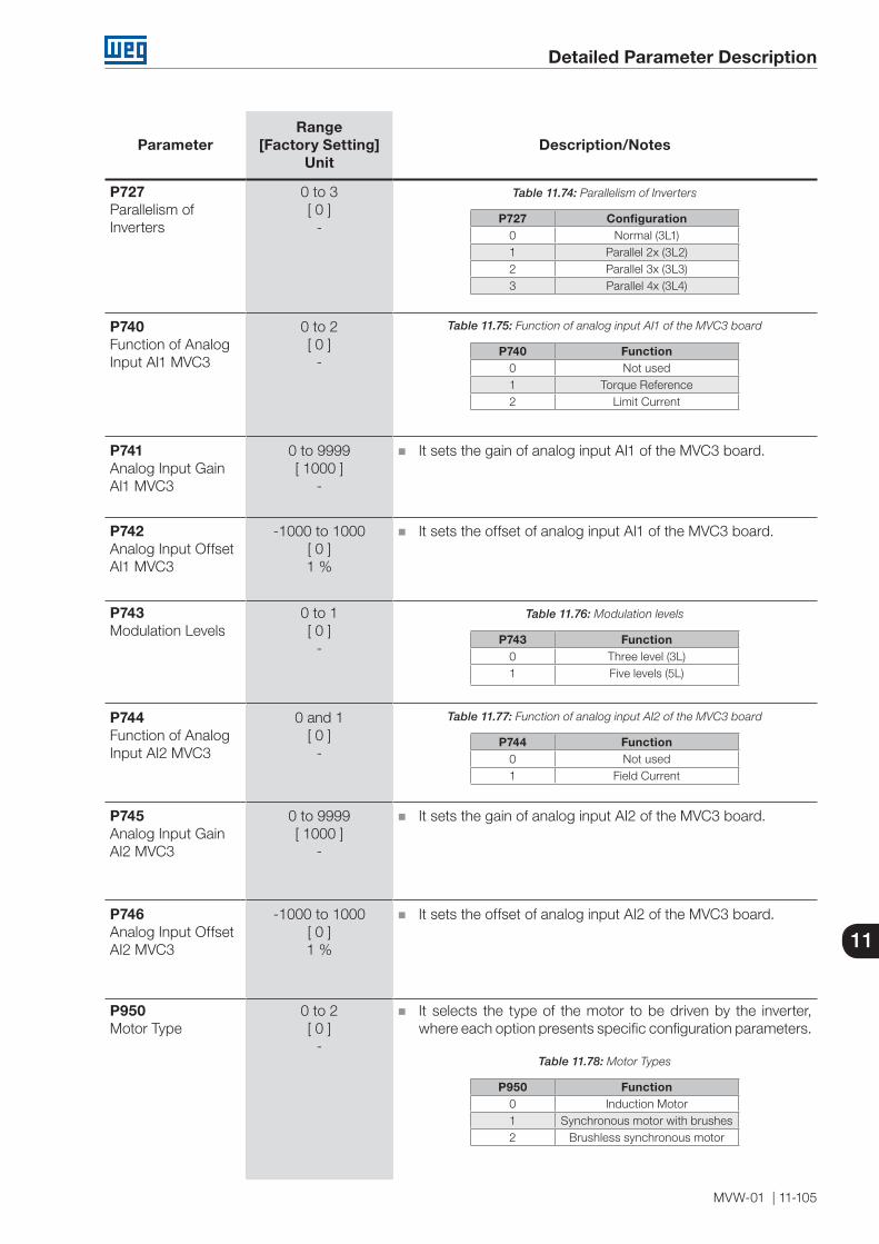
Detailed Parameter Description
MVW-01 | 11-105
11
ParameterRange
[Factory Setting]Unit
Description/Notes
P727Parallelism of Inverters
0 to 3[ 0 ]
-
Table 11.74: Parallelism of Inverters
P727 Configuration0 Normal (3L1)1 Parallel 2x (3L2)2 Parallel 3x (3L3)3 Parallel 4x (3L4)
P740Function of Analog Input AI1 MVC3
0 to 2[ 0 ]
-
Table 11.75: Function of analog input AI1 of the MVC3 board
P740 Function0 Not used1 Torque Reference2 Limit Current
P741Analog Input Gain AI1 MVC3
0 to 9999[ 1000 ]
-
It sets the gain of analog input AI1 of the MVC3 board.
P742Analog Input Offset AI1 MVC3
-1000 to 1000[ 0 ]1 %
It sets the offset of analog input AI1 of the MVC3 board.
P743Modulation Levels
0 to 1[ 0 ]
-
Table 11.76: Modulation levels
P743 Function0 Three level (3L)1 Five levels (5L)
P744Function of Analog Input AI2 MVC3
0 and 1[ 0 ]
-
Table 11.77: Function of analog input AI2 of the MVC3 board
P744 Function0 Not used1 Field Current
P745Analog Input Gain AI2 MVC3
0 to 9999[ 1000 ]
-
It sets the gain of analog input AI2 of the MVC3 board.
P746Analog Input Offset AI2 MVC3
-1000 to 1000[ 0 ]1 %
It sets the offset of analog input AI2 of the MVC3 board.
P950Motor Type
0 to 2[ 0 ]
-
It selects the type of the motor to be driven by the inverter, where each option presents specific configuration parameters.
Table 11.78: Motor Types
P950 Function0 Induction Motor1 Synchronous motor with brushes2 Brushless synchronous motor

Detailed Parameter Description
11-106 | MVW-01
11
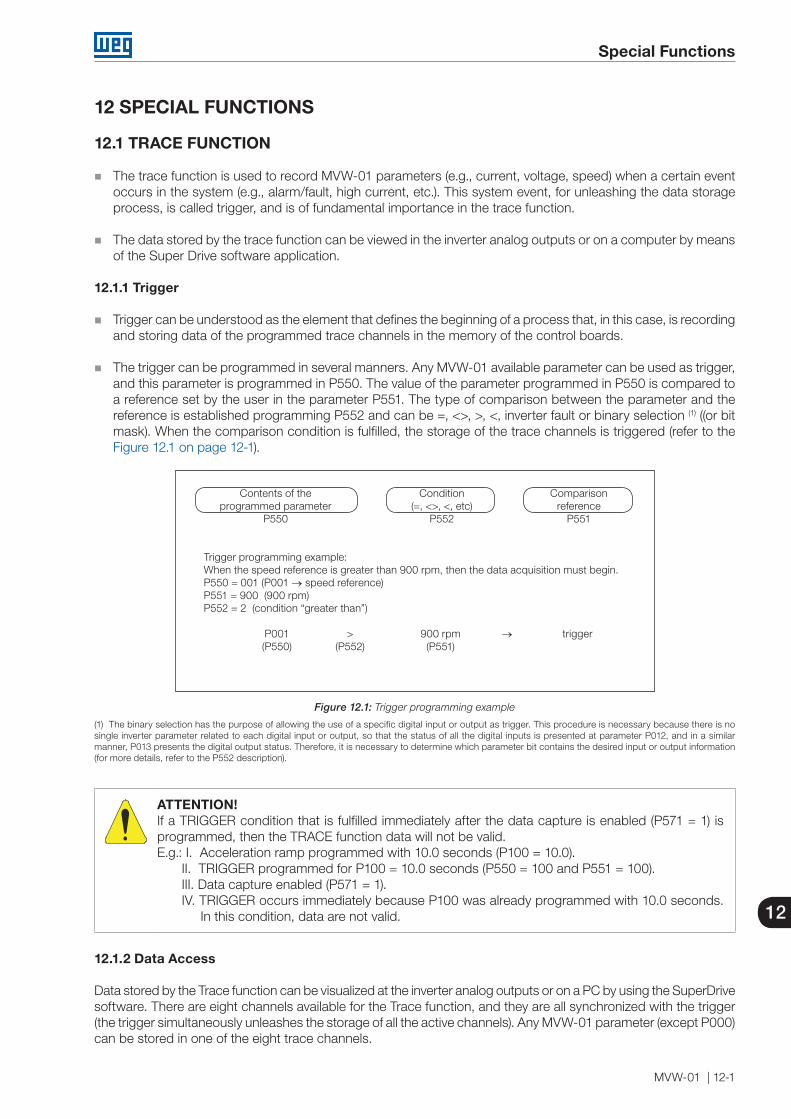
Special Functions
MVW-01 | 12-1
12
12 SPECIAL FUNCTIONS
12.1 TRACE FUNCTION
The trace function is used to record MVW-01 parameters (e.g., current, voltage, speed) when a certain event occurs in the system (e.g., alarm/fault, high current, etc.). This system event, for unleashing the data storage process, is called trigger, and is of fundamental importance in the trace function.
The data stored by the trace function can be viewed in the inverter analog outputs or on a computer by means of the Super Drive software application.
12.1.1 Trigger
Trigger can be understood as the element that defines the beginning of a process that, in this case, is recording and storing data of the programmed trace channels in the memory of the control boards.
The trigger can be programmed in several manners. Any MVW-01 available parameter can be used as trigger, and this parameter is programmed in P550. The value of the parameter programmed in P550 is compared to a reference set by the user in the parameter P551. The type of comparison between the parameter and the reference is established programming P552 and can be =, <>, >, <, inverter fault or binary selection (1) ((or bit mask). When the comparison condition is fulfilled, the storage of the trace channels is triggered (refer to the Figure 12.1 on page 12-1).
Contents of the Condition Comparison programmed parameter (=, <>, <, etc) reference P550 P552 P551
Trigger programming example:When the speed reference is greater than 900 rpm, then the data acquisition must begin.P550 = 001 (P001 → speed reference)P551 = 900 (900 rpm)P552 = 2 (condition “greater than”)
P001 > 900 rpm → trigger (P550) (P552) (P551)
Figure 12.1: Trigger programming example
(1) The binary selection has the purpose of allowing the use of a specific digital input or output as trigger. This procedure is necessary because there is no single inverter parameter related to each digital input or output, so that the status of all the digital inputs is presented at parameter P012, and in a similar manner, P013 presents the digital output status. Therefore, it is necessary to determine which parameter bit contains the desired input or output information (for more details, refer to the P552 description).
ATTENTION!If a TRIGGER condition that is fulfilled immediately after the data capture is enabled (P571 = 1) is programmed, then the TRACE function data will not be valid.E.g.: I. Acceleration ramp programmed with 10.0 seconds (P100 = 10.0).
II. TRIGGER programmed for P100 = 10.0 seconds (P550 = 100 and P551 = 100).III. Data capture enabled (P571 = 1).IV. TRIGGER occurs immediately because P100 was already programmed with 10.0 seconds.
In this condition, data are not valid.
12.1.2 Data Access
Data stored by the Trace function can be visualized at the inverter analog outputs or on a PC by using the SuperDrive software. There are eight channels available for the Trace function, and they are all synchronized with the trigger (the trigger simultaneously unleashes the storage of all the active channels). Any MVW-01 parameter (except P000) can be stored in one of the eight trace channels.
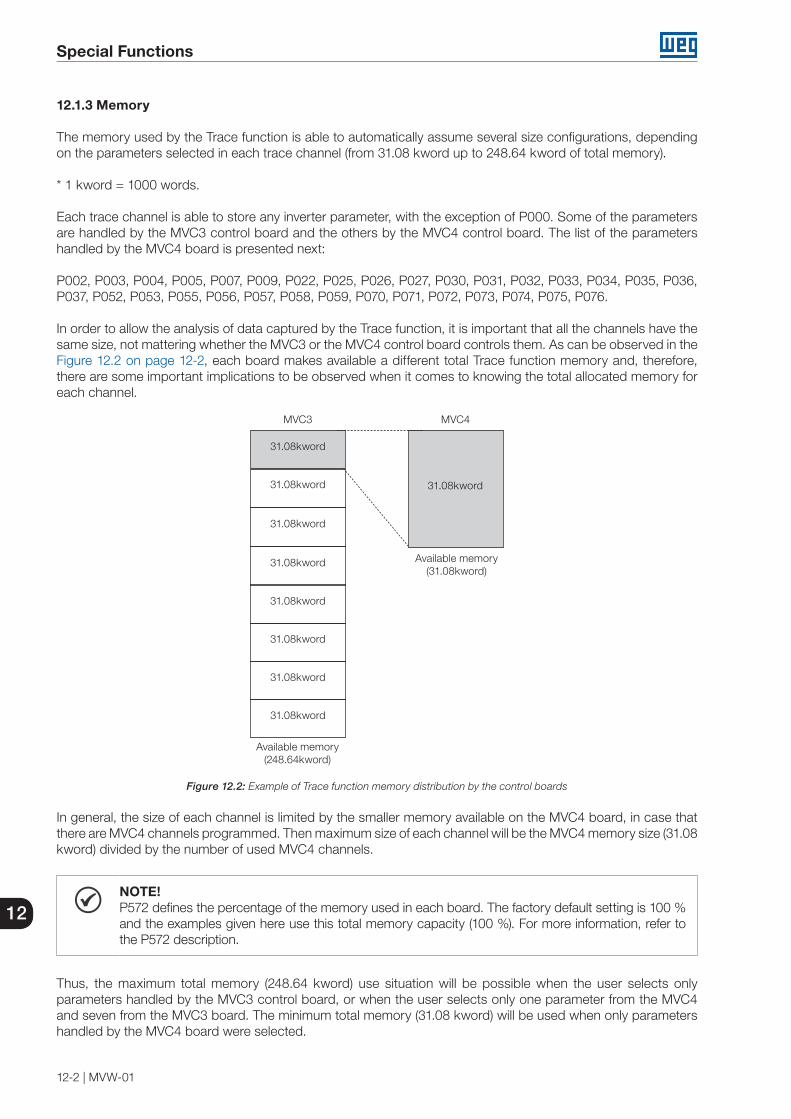
Special Functions
12-2 | MVW-01
12
12.1.3 Memory
The memory used by the Trace function is able to automatically assume several size configurations, depending on the parameters selected in each trace channel (from 31.08 kword up to 248.64 kword of total memory).
* 1 kword = 1000 words.
Each trace channel is able to store any inverter parameter, with the exception of P000. Some of the parameters are handled by the MVC3 control board and the others by the MVC4 control board. The list of the parameters handled by the MVC4 board is presented next:
P002, P003, P004, P005, P007, P009, P022, P025, P026, P027, P030, P031, P032, P033, P034, P035, P036, P037, P052, P053, P055, P056, P057, P058, P059, P070, P071, P072, P073, P074, P075, P076.
In order to allow the analysis of data captured by the Trace function, it is important that all the channels have the same size, not mattering whether the MVC3 or the MVC4 control board controls them. As can be observed in the Figure 12.2 on page 12-2, each board makes available a different total Trace function memory and, therefore, there are some important implications to be observed when it comes to knowing the total allocated memory for each channel.
MVC3 MVC4
31.08kword
31.08kword
31.08kword
31.08kword
31.08kword
31.08kword
31.08kword
31.08kword
31.08kword
Available memory(248.64kword)
Available memory (31.08kword)
Figure 12.2: Example of Trace function memory distribution by the control boards
In general, the size of each channel is limited by the smaller memory available on the MVC4 board, in case that there are MVC4 channels programmed. Then maximum size of each channel will be the MVC4 memory size (31.08 kword) divided by the number of used MVC4 channels.
NOTE!P572 defines the percentage of the memory used in each board. The factory default setting is 100 % and the examples given here use this total memory capacity (100 %). For more information, refer to the P572 description.
Thus, the maximum total memory (248.64 kword) use situation will be possible when the user selects only parameters handled by the MVC3 control board, or when the user selects only one parameter from the MVC4 and seven from the MVC3 board. The minimum total memory (31.08 kword) will be used when only parameters handled by the MVC4 board were selected.

Special Functions
MVW-01 | 12-3
12
In any other case an intermediate size configuration will be used, limited by the memory available in the MVC4 board and depending, therefore, on the number of channels with MVC4 parameters. In this way, the memory is distributed according to the number of active channels on each board.
EXAMPLE 1: trace function programmed for 3 MVC4 channels.
MVC4 RAM= 31.08kword.RAM area per MVC4 channel = 31.08 / 3 = 10.36kword.RAM area per MVC3 channel = 0kword.RAM area per channel = 10.36kword → 10360 points per channel.Total RAM use = 3 x 10.36kword = 31.08kword.
Therefore, the MVC4 board handles 3 channels, witch use 10.36 kword of memory each one.
The MVC3 control board has a memory capacity 8 times greater than the MVC4; therefore, the memory reserved for each channel handled by the MVC3 is equal to the size of each channel handled by the MVC4, regardless of the allocated RAM memory area size. If there are no channels handled by the MVC4 board, then the size of each MVC3 handled channel is equal to the total RAM area (248.64 kword) divided by the number of programmed channels.
EXAMPLE 2: trace function programmed with 4 MVC4 handled channels and 2 MVC3 channels.
MVC4 RAM = 31.08kword.RAM area per MVC4 channel = 31.08 / 4 = 7.77kword.RAM area per MVC3 channel = 7.77kword.RAM area per channel = 7.77kword → 7770 points per channel.Total RAM use = 6 x 7.77kword = 46.62kword.
12.1.4 Sampling
Sampling time is the time interval between the points stored by the Trace function (refer to the Figure 12.3 on page 12-3). If, for instance, a 1 ms (1 millisecond or 1/1000 second), it means that 1000 points will be stored per second (if there is enough memory available).
The sampling time is the same for all the channels programmed in the Trace function, and it can be programmed as a whole number multiplying 500 μs. If a 2 ms sampling time (4 x 500 μs) is programmed for the example 2, then 15.54 seconds of information will be stored in each channel (7770 x 2 ms).
i (t)in
i0
i1
i2
i3 i4
Ta
Ta= Sampling time(t)
Figure 12.3: Example of Trace function signal sampling
12.1.5 Pre-Trigger
It is possible to program a pre-trigger time as a percentage of the total record (see the Figure 12.4 on page 12-4), meaning that part of the Trace function data before the trigger event will be stored. If a 50 % pre-trigger is programmed for the example 2, then 7.77 sec data before the trigger and 7.77 sec after, will be stored.
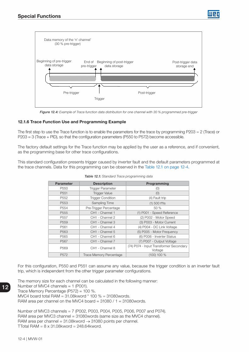
Special Functions
12-4 | MVW-01
12
Data memory of the ‘n’ channel’(30 % pre-trigger)
Beginning of pre-triggerdata storage
End ofpre-trigger
Post-trigger datastorage end
Beginning of post-triggerdata storage
Pre-trigger Post-trigger
Trigger
Figure 12.4: Example of Trace function data distribution for one channel with 30 % programmed pre-trigger
12.1.6 Trace Function Use and Programming Example
The first step to use the Trace function is to enable the parameters for the trace by programming P203 = 2 (Trace) or P203 = 3 (Trace + PID), so that the configuration parameters (P550 to P572) become accessible.
The factory default settings for the Trace function may be applied by the user as a reference, and if convenient, as the programming base for other trace configurations.
This standard configuration presents trigger caused by inverter fault and the default parameters programmed at the trace channels. Data for this programming can be observed in the Table 12.1 on page 12-4.
Table 12.1: Standard Trace programming data
Parameter Description ProgrammingP550 Trigger Parameter (0)P551 Trigger Value (0)P552 Trigger Condition (4) Fault trip
P553 Sampling Time (1) 500 msP554 Pre-Trigger Percentage 50 %P555 CH1 - Channel 1 (1) P001 - Speed ReferenceP557 CH1 - Channel 2 (2) P002 - Motor SpeedP559 CH1 - Channel 3 (3) P003 - Motor CurrentP561 CH1 - Channel 4 (4) P004 - DC Link VoltageP563 CH1 - Channel 5 (5) P005 - Motor FrequencyP565 CH1 - Channel 6 (6) P006 - Inverter StatusP567 CH1 - Channel 7 (7) P007 - Output Voltage
P569 CH1 - Channel 8(74) P074 - Input Transformer Secondary
VoltageP572 Trace Memory Percentage (100) 100 %
For this configuration, P550 and P551 can assume any value, because the trigger condition is an inverter fault trip, which is independent from the other trigger parameter configurations.
The memory size for each channel can be calculated in the following manner:Number of MVC4 channels = 1 (P001).Trace Memory Percentage (P572) = 100 %.MVC4 board total RAM = 31.08kword * 100 % = 31080words.RAM area per channel on the MVC4 board = 31080 / 1 = 31080words.
Number of MVC3 channels = 7 (P002, P003, P004, P005, P006, P007 and P074).RAM area per MVC3 channel = 31080words (same size as the MVC4 channel).RAM area per channel = 31.08kword → 31080 points per channel.TTotal RAM = 8 x 31.08kword = 248.64kword.
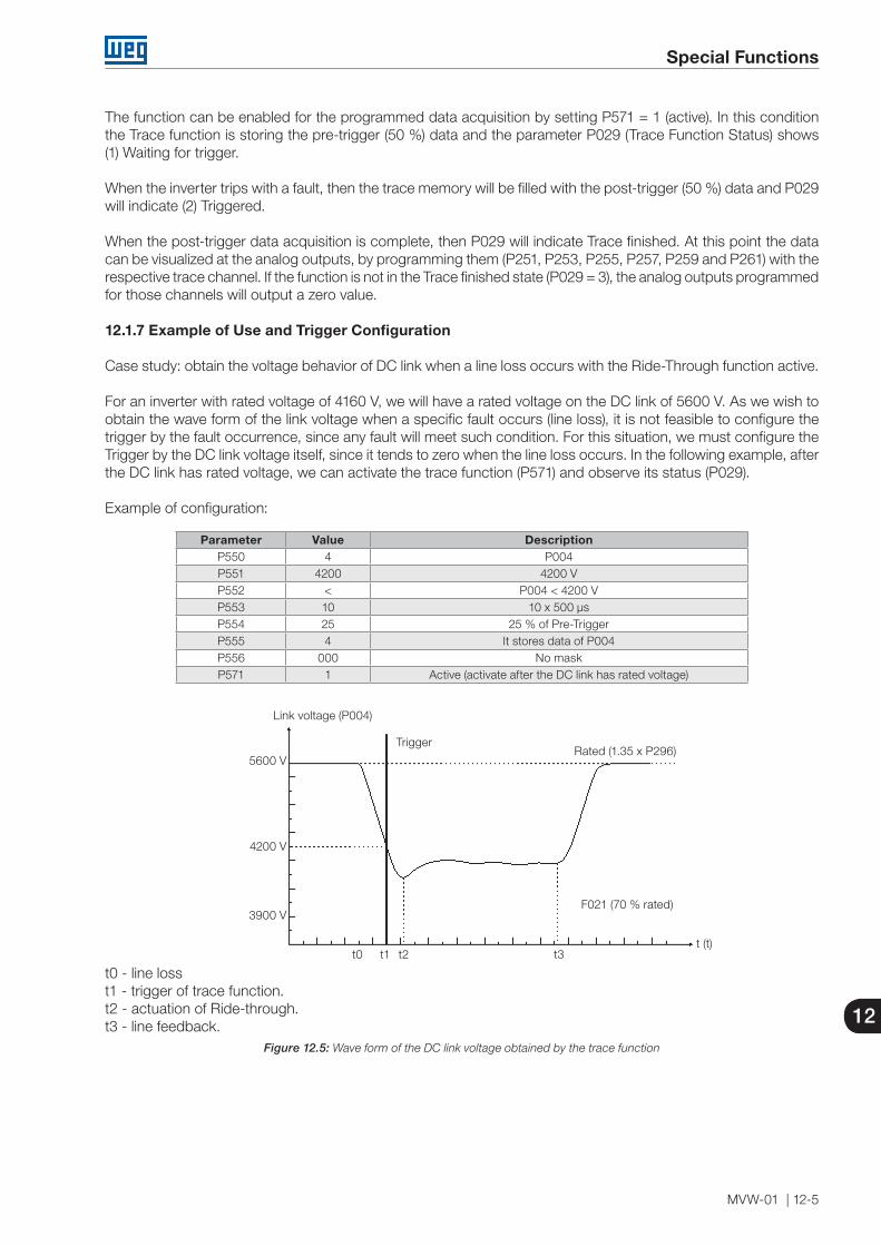
Special Functions
MVW-01 | 12-5
12
The function can be enabled for the programmed data acquisition by setting P571 = 1 (active). In this condition the Trace function is storing the pre-trigger (50 %) data and the parameter P029 (Trace Function Status) shows (1) Waiting for trigger.
When the inverter trips with a fault, then the trace memory will be filled with the post-trigger (50 %) data and P029 will indicate (2) Triggered.
When the post-trigger data acquisition is complete, then P029 will indicate Trace finished. At this point the data can be visualized at the analog outputs, by programming them (P251, P253, P255, P257, P259 and P261) with the respective trace channel. If the function is not in the Trace finished state (P029 = 3), the analog outputs programmed for those channels will output a zero value.
12.1.7 Example of Use and Trigger Configuration
Case study: obtain the voltage behavior of DC link when a line loss occurs with the Ride-Through function active.
For an inverter with rated voltage of 4160 V, we will have a rated voltage on the DC link of 5600 V. As we wish to obtain the wave form of the link voltage when a specific fault occurs (line loss), it is not feasible to configure the trigger by the fault occurrence, since any fault will meet such condition. For this situation, we must configure the Trigger by the DC link voltage itself, since it tends to zero when the line loss occurs. In the following example, after the DC link has rated voltage, we can activate the trace function (P571) and observe its status (P029).
Example of configuration:
Parameter Value DescriptionP550 4 P004P551 4200 4200 VP552 < P004 < 4200 VP553 10 10 x 500 µsP554 25 25 % of Pre-TriggerP555 4 It stores data of P004P556 000 No maskP571 1 Active (activate after the DC link has rated voltage)
Trigger
5600 V
4200 V
3900 V
t0 t1 t2 t3t (t)
Rated (1.35 x P296)
F021 (70 % rated)
Link voltage (P004)
t0 - line losst1 - trigger of trace function.t2 - actuation of Ride-through.t3 - line feedback.
Figure 12.5: Wave form of the DC link voltage obtained by the trace function

Special Functions
12-6 | MVW-01
12
12.2 PID REGULATOR
The MVW-01 has a PID regulator function, which can be used to control a closed loop process. That function consists of a controller with proportional, integral and derivative gain, superposed to the normal MVW-01 speed control.
In order to keep the process variable (the one to be controlled - water level in a reservoir for instance) at the value adjusted with the setpoint, the speed will be varied automatically by the PID controller.
That regulator is able, for instance, to control the flow in a pipeline by means of flow feedback applied to the analog input AI2 or AI3 (selected through P524) and setpoint according to P221 or P222 definition (e.g., AI1), with the inverter driving the pump that is responsible for the pipeline flow.
Other application examples are: Level or temperature control, dosage, etc.
The PID regulator function is activated by setting P203 = 1 or 3.
The Figure 12.6 on page 12-8 presents the Academic PID Regulator block diagram.
The Academic PID Regulator transference function in the frequency domain is:
y(s) = Kp e(s) [1 + 1 + sTd]
sTi
Replacing the integrator by a sum and the derivative by the incremental quotient, we will obtain an approximate value for the discrete (recursive) transfer equation shown next:
y(kTa) = y(k-1)Ta + Kp[(e(kTa) - e(k-1)Ta) + Kie(k-1)Ta + Kd(e(kTa) -2e(k-1)Ta + e(k-2)Ta)]
Where:Kp (Proportional Gain): Kp = P520 x 4096.Ki (Integral Gain): Ki = P521 x 4096 = [Ta/Ti x 4096 ].Kd (Differential Gain): Kd = P522 x 4096 = [Td/Ta x 4096].Ta = 0.02 sec (PID regulator sampling time).SP*: reference, maximum 13 bits (0 to 8191).X: process variable (or controlled), read through AI2 or AI3, maximum 13 bits.y( kTa): current PID output, maximum 13 bits.y(k-1)Ta: previous PID output.e( kTa): current error [SP*( k) - X( k)].e(k-1)Ta: previous error [SP*( k-1) - X( k-1)].e(k-2)Ta: error at two previous samplings [SP*( k-2) - X( k-2)].
The feedback signal must be connected to the analog input AI2’ and AI3’ (refer to the Figure 11.32 on page 11-53 and Figure 12.6 on page 12-8).The setpoint can be defined via:
Keypad: parameter P525.
Analog input AI1’, AI2’, AI3’, AI4’, AI5’, (AI1’+ AI2’)>0, (AI1’+ AI2’), Multispeed, Serial, Fieldbus.Note: When P203 = 1 or 3, do not use the reference via EP P221/P222 = 7.
When the PID function is enabled (P203 = 1 or 3):
One of the digital inputs from DI3 to DI10 can select between manual and automatic PID operation (P265 to P272).

Special Functions
MVW-01 | 12-7
12
When the PID regulator function is activated (P203 = 1 or 3), the digital input DI3 is automatically programmed for the Manual/Automatic function (P265 = 15):
Table 12.2: DIx operation mode
DIx PID status0 (0V) Manual1 (24V) Automatic
P040 indicates the process variable value (feedback) in the selected scale and unit. In order to avoid the feedback analog input saturation during a regulation overshoot, the signal must vary between 0 and 9.0 V (0(4) to 18 mA). The adaptation between the setpoint and the feedback can be done changing the gain of the analog input selected as feedback (P238 for AI2 or P242 for AI3). The Process variable can also be visualized at the outputs AO1 to AO6, if it has been programmed at P251, P253, P255, P257, P259 and P261. This is also valid for the PID setpoint.
The outputs DO1, DO2 and RL1 to RL5, can be programmed (P275 to P277, P279 to P282) for the functions Process Variable > VPx (P533) and Process Variable < VPy (P534).
The functions JOG and Forward/Reverse remain disabled. Enable and Start/Stop commands are defined at P220, P224 and P227.
If the setpoint is defined by P525 (P221 or P222 = 0), and the system is changed from manual to automatic, then P525 is automatically adjusted with the P040 value. In this case the transition from manual to automatic is smooth (there is no abrupt speed variation).

Special Functions
12-8 | MVW-01
12
Set
poin
t def
initi
on (p
roce
ss v
aria
ble
refe
renc
e)
P52
5
Set
poin
t (S
P)
Not
e 1
Not
e 2
Not
e1:
P22
1/P
222
= 0
(K
eypa
d se
tpoi
nt)
Not
e2: P
221/
P22
2 =
1 to
11
(Set
poin
t via
Ana
log
Inpu
ts, M
ultis
peed
,S
eria
l, Fi
eldb
us a
nd P
LC b
oard
)
Ena
ble
AI2
'
AI3
'
Feed
back
P52
4 (re
fer
to th
e
Figu
re 1
1.31
on
page
11-
52 a
nd
Figu
re 1
1.32
on
page
11-
53)
P52
6
P04
0
+
-A
cade
mic
PID
P13
3, P
134
P52
7
0 =
Dire
ct
1 =
Rev
erse
PID
reg
ulat
orac
tion
Man
ual (
Ope
n D
Ix)
Aut
omat
ic(C
lose
d D
Ix)
DI3
(P26
5 =
15)
Aca
dem
ic P
IDP
522
P52
1
+ +
+
Spe
edre
fere
nce
(refe
r to
the
Fig
ure
11.2
6 on
pag
e 11
-48)
P52
0
Ena
ble
Ref
eren
ce(re
fer
to th
e Fi
gure
11.
25
on p
age
11-4
7)
P52
3
Figure 12.6: Academic PID regulator block diagram
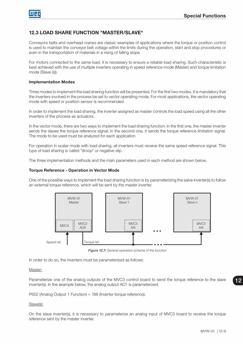
Special Functions
MVW-01 | 12-9
12
12.3 LOAD SHARE FUNCTION "MASTER/SLAVE"
Conveyors belts and overhead cranes are classic examples of applications where the torque or position control is used to maintain the conveyor belt voltage within the limits during the operation, start and stop procedures or even in the transportation of materials in a rising of falling slope.
For motors connected to the same load, it is necessary to ensure a reliable load sharing. Such characteristic is best achieved with the use of multiple inverters operating in speed reference mode (Master) and torque limitation mode (Slave (s)).
Implementation Modes
Three modes to implement the load sharing function will be presented. For the first two modes, it is mandatory that the inverters involved in the process be set to vector operating mode. For most applications, the vector operating mode with speed or position sensor is recommended.
In order to implement the load sharing, the inverter assigned as master controls the load speed using all the other inverters of the process as actuators.
In the vector mode, there are two ways to implement the load sharing function: in the first one, the master inverter sends the slaves the torque reference signal; in the second one, it sends the torque reference limitation signal. The mode to be used must be analyzed for each application.
For operation in scalar mode with load sharing, all inverters must receive the same speed reference signal. This type of load sharing is called "droop" or negative slip.
The three implementation methods and the main parameters used in each method are shown below.
Torque Reference - Operation in Vector Mode
One of the possible ways to implement the load sharing function is by parameterizing the salve inverter(s) to follow an external torque reference, which will be sent by the master inverter.
......
MVW-01Master
Speed ref. Torque ref.
MVC4MVC3AOX
MVC3AIX
MVC3AIX
MVW-01Slave 1
MVW-01Slave n
Figure 12.7: General operation scheme of the function
In order to do so, the inverters must be parameterized as follows:
Master:
Parameterize one of the analog outputs of the MVC3 control board to send the torque reference to the slave inverter(s). In the example below, the analog output AO1 is parameterized.
P652 (Analog Output 1 Function) = 188 (Inverter torque reference).
Slave(s):
On the slave inverter(s), it is necessary to parameterize an analog input of MVC3 board to receive the torque reference sent by the master inverter.
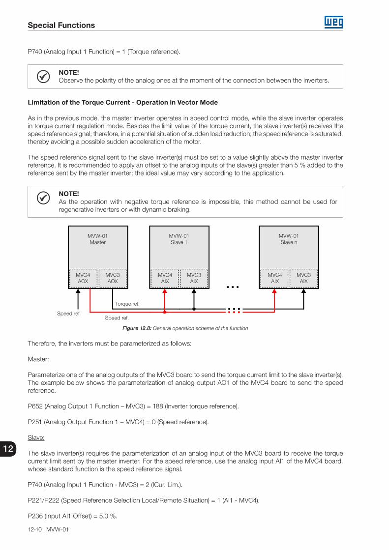
Special Functions
12-10 | MVW-01
12
P740 (Analog Input 1 Function) = 1 (Torque reference).
NOTE!Observe the polarity of the analog ones at the moment of the connection between the inverters.
Limitation of the Torque Current - Operation in Vector Mode
As in the previous mode, the master inverter operates in speed control mode, while the slave inverter operates in torque current regulation mode. Besides the limit value of the torque current, the slave inverter(s) receives the speed reference signal; therefore, in a potential situation of sudden load reduction, the speed reference is saturated, thereby avoiding a possible sudden acceleration of the motor.
The speed reference signal sent to the slave inverter(s) must be set to a value slightly above the master inverter reference. It is recommended to apply an offset to the analog inputs of the slave(s) greater than 5 % added to the reference sent by the master inverter; the ideal value may vary according to the application.
NOTE!As the operation with negative torque reference is impossible, this method cannot be used for regenerative inverters or with dynamic braking.
.........
MVW-01Master
Speed ref.Speed ref.
Torque ref.
MVC4AOX
MVC3AOX
MVC3AIX
MVC4AIX
MVC4AIX
MVC3AIX
MVW-01Slave 1
MVW-01Slave n
Figure 12.8: General operation scheme of the function
Therefore, the inverters must be parameterized as follows:
Master:
Parameterize one of the analog outputs of the MVC3 board to send the torque current limit to the slave inverter(s). The example below shows the parameterization of analog output AO1 of the MVC4 board to send the speed reference.
P652 (Analog Output 1 Function – MVC3) = 188 (Inverter torque reference).
P251 (Analog Output Function 1 – MVC4) = 0 (Speed reference).
Slave:
The slave inverter(s) requires the parameterization of an analog input of the MVC3 board to receive the torque current limit sent by the master inverter. For the speed reference, use the analog input AI1 of the MVC4 board, whose standard function is the speed reference signal.
P740 (Analog Input 1 Function - MVC3) = 2 (ICur. Lim.).
P221/P222 (Speed Reference Selection Local/Remote Situation) = 1 (AI1 - MVC4).
P236 (Input AI1 Offset) = 5.0 %.
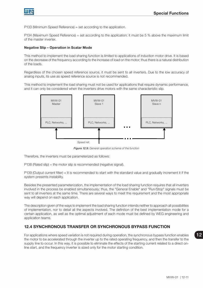
Special Functions
MVW-01 | 12-11
12
P133 (Minimum Speed Reference) = set according to the application.
P134 (Maximum Speed Reference) = set according to the application; it must be 5 % above the maximum limit of the master inverter.
Negative Slip – Operation in Scalar Mode
This method to implement the load sharing function is limited to applications of induction motor drive. It is based on the decrease of the frequency according to the increase of load on the motor; thus there is a natural distribution of the loads.
Regardless of the chosen speed reference source, it must be sent to all inverters. Due to the low accuracy of analog inputs, its use as speed reference source is not recommended.
This method to implement the load sharing must not be used for applications that require dynamic performance, and it can only be considered when the inverters drive motors with the same characteristic slip.
...
Mestre Escravo 1 Escravo n
MVC3AOx
...
MVC3AIx
MVC3AIx
MVC4AOx
MVC4AIx
MVC4AIx...
......
Mestre Escravo 1 Escravo n
MVC3AOx
...
MVC3AIx
MVC3AIx
MVC4AOx
MVC4AIx
MVC4AIx...
...
MVW-01Master
Speed ref.
PLC, Networks, ... PLC, Networks, ... PLC, Networks, ...
MVW-01Slave 1
MVW-01Slave n
Figure 12.9: General operation scheme of the function
Therefore, the inverters must be parameterized as follows:
P138 (Rated slip) = the motor slip is recommended (negative signal).
P139 (Output current filter) = it is recommended to start with the standard value and gradually increment it if the system presents instability.
Besides the presented parameterization, the implementation of the load sharing function requires that all inverters involved in the process be enabled simultaneously; thus, the "General Enable" and "Run/Stop" signals must be sent to all inverters at the same time. There are several ways to meet this requirement and the most appropriate way will depend on each application.
The description given of the ways to implement the load sharing function intends neither to approach all possibilities of implementation, nor to detail all the aspects involved. The definition of the best implementation mode for a certain application, as well as the optimal adjustment of each mode must be defined by WEG engineering and application teams.
12.4 SYNCHRONOUS TRANSFER OR SYNCHRONOUS BYPASS FUNCTION
For applications where speed variation is not required during operation, the synchronous bypass function enables the motor to be accelerated through the inverter up to the rated operating frequency, and then the transfer to the supply line to occur. In this way, it is possible to eliminate the effects of the starting current related to a direct on-line start, and the frequency inverter is sized only for the motor starting condition.
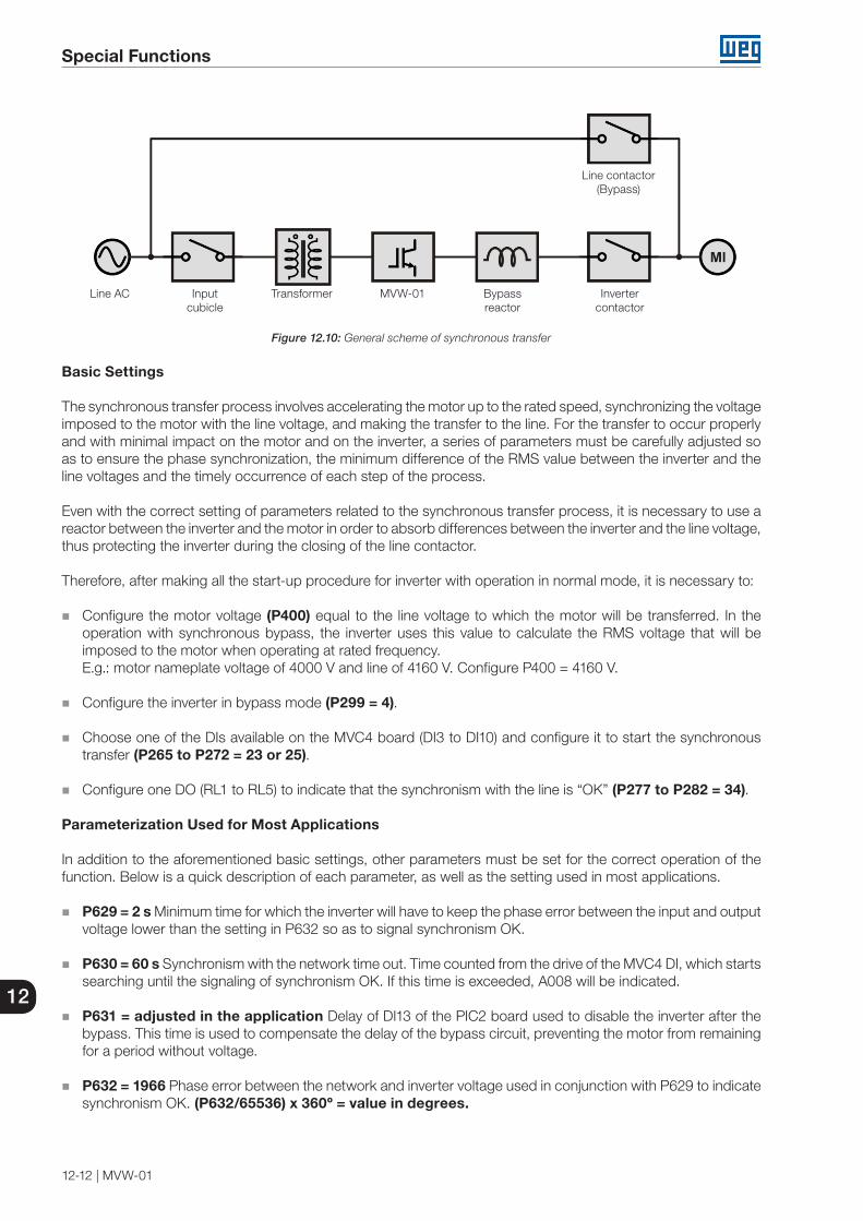
Special Functions
12-12 | MVW-01
12
Line AC Input cubicle
Transformer MVW-01 Bypass reactor
Inverter contactor
Line contactor(Bypass)
Figure 12.10: General scheme of synchronous transfer
Basic Settings
The synchronous transfer process involves accelerating the motor up to the rated speed, synchronizing the voltage imposed to the motor with the line voltage, and making the transfer to the line. For the transfer to occur properly and with minimal impact on the motor and on the inverter, a series of parameters must be carefully adjusted so as to ensure the phase synchronization, the minimum difference of the RMS value between the inverter and the line voltages and the timely occurrence of each step of the process.
Even with the correct setting of parameters related to the synchronous transfer process, it is necessary to use a reactor between the inverter and the motor in order to absorb differences between the inverter and the line voltage, thus protecting the inverter during the closing of the line contactor.
Therefore, after making all the start-up procedure for inverter with operation in normal mode, it is necessary to:
Configure the motor voltage (P400) equal to the line voltage to which the motor will be transferred. In the operation with synchronous bypass, the inverter uses this value to calculate the RMS voltage that will be imposed to the motor when operating at rated frequency.
E.g.: motor nameplate voltage of 4000 V and line of 4160 V. Configure P400 = 4160 V.
Configure the inverter in bypass mode (P299 = 4).
Choose one of the DIs available on the MVC4 board (DI3 to DI10) and configure it to start the synchronous transfer (P265 to P272 = 23 or 25).
Configure one DO (RL1 to RL5) to indicate that the synchronism with the line is “OK” (P277 to P282 = 34).
Parameterization Used for Most Applications
In addition to the aforementioned basic settings, other parameters must be set for the correct operation of the function. Below is a quick description of each parameter, as well as the setting used in most applications.
P629 = 2 s Minimum time for which the inverter will have to keep the phase error between the input and output voltage lower than the setting in P632 so as to signal synchronism OK.
P630 = 60 s Synchronism with the network time out. Time counted from the drive of the MVC4 DI, which starts searching until the signaling of synchronism OK. If this time is exceeded, A008 will be indicated.
P631 = adjusted in the application Delay of DI13 of the PIC2 board used to disable the inverter after the bypass. This time is used to compensate the delay of the bypass circuit, preventing the motor from remaining for a period without voltage.
P632 = 1966 Phase error between the network and inverter voltage used in conjunction with P629 to indicate synchronism OK. (P632/65536) x 360º = value in degrees.
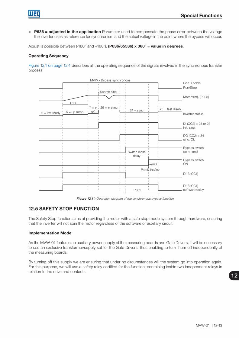
Special Functions
MVW-01 | 12-13
12
P636 = adjusted in the application Parameter used to compensate the phase error between the voltage the inverter uses as reference for synchronism and the actual voltage in the point where the bypass will occur.
Adjust is possible between (-180° and +180º). (P636/65536) x 360º = value in degrees.
Operating Sequency
Figure 12.1 on page 12-1 describes all the operating sequence of the signals involved in the synchronous transfer process.
2 = inv. ready
26 = in sync. 25 = fast disab24 = sync.
Search sinc.
5 = up ramp
Paral. line/inv
Gen. EnableRun/Stop
Motor freq. (P005)
Inverter status
DI (CC2) = 25 or 23 init. sinc.
DO (CC2) = 34 sinc. Ok
Bypass switch command
Bypass switch ON
Switch close delay
P631
∼2mS
DI13 (CC1)
DI13 (CC1) software delay
P1007 = in ref.
MVW - Bypass synchronous
Figure 12.11: Operation diagram of the synchronous bypass function
12.5 SAFETY STOP FUNCTION
The Safety Stop function aims at providing the motor with a safe stop mode system through hardware, ensuring that the inverter will not spin the motor regardless of the software or auxiliary circuit.
Implementation Mode
As the MVW-01 features an auxiliary power supply of the measuring boards and Gate Drivers, it will be necessary to use an exclusive transformer/supply set for the Gate Drivers, thus enabling to turn them off independently of the measuring boards.
By turning off this supply we are ensuring that under no circumstances will the system go into operation again. For this purpose, we will use a safety relay certified for the function, containing inside two independent relays in relation to the drive and contacts.
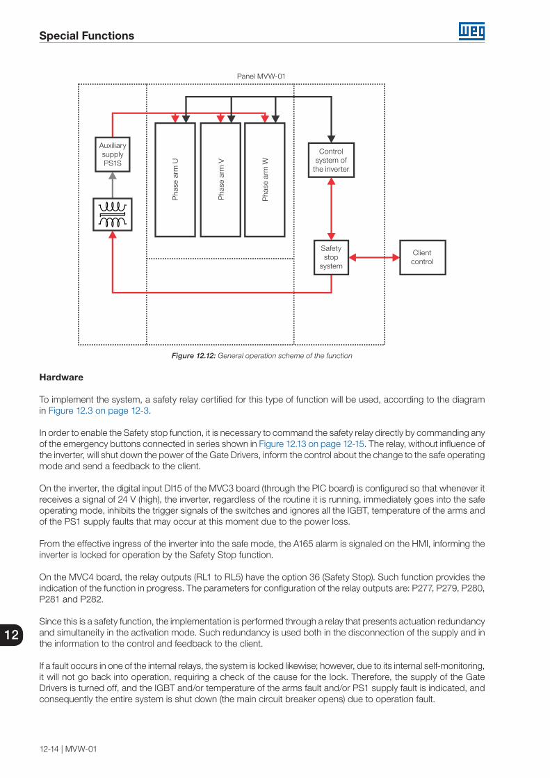
Special Functions
12-14 | MVW-01
12
Control system of
the inverterP
hase
arm
U
Pha
se a
rm V
Pha
se a
rm W
Safety stop
system
Client control
Auxiliary supply PS1S
Panel MVW-01
Figure 12.12: General operation scheme of the function
Hardware
To implement the system, a safety relay certified for this type of function will be used, according to the diagram in Figure 12.3 on page 12-3.
In order to enable the Safety stop function, it is necessary to command the safety relay directly by commanding any of the emergency buttons connected in series shown in Figure 12.13 on page 12-15. The relay, without influence of the inverter, will shut down the power of the Gate Drivers, inform the control about the change to the safe operating mode and send a feedback to the client.
On the inverter, the digital input DI15 of the MVC3 board (through the PIC board) is configured so that whenever it receives a signal of 24 V (high), the inverter, regardless of the routine it is running, immediately goes into the safe operating mode, inhibits the trigger signals of the switches and ignores all the IGBT, temperature of the arms and of the PS1 supply faults that may occur at this moment due to the power loss.
From the effective ingress of the inverter into the safe mode, the A165 alarm is signaled on the HMI, informing the inverter is locked for operation by the Safety Stop function.
On the MVC4 board, the relay outputs (RL1 to RL5) have the option 36 (Safety Stop). Such function provides the indication of the function in progress. The parameters for configuration of the relay outputs are: P277, P279, P280, P281 and P282.
Since this is a safety function, the implementation is performed through a relay that presents actuation redundancy and simultaneity in the activation mode. Such redundancy is used both in the disconnection of the supply and in the information to the control and feedback to the client.
If a fault occurs in one of the internal relays, the system is locked likewise; however, due to its internal self-monitoring, it will not go back into operation, requiring a check of the cause for the lock. Therefore, the supply of the Gate Drivers is turned off, and the IGBT and/or temperature of the arms fault and/or PS1 supply fault is indicated, and consequently the entire system is shut down (the main circuit breaker opens) due to operation fault.
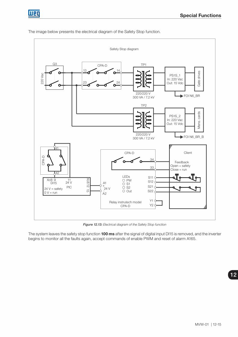
Special Functions
MVW-01 | 12-15
12
The image below presents the electrical diagram of the Safety Stop function.
Client
PS1S_2 In: 220 VacOut: 15 Vdc
PS1S_1 In: 220 Vac Out: 15 Vdc
Relay instrutech model CPA-D
Feedback
FOI N6_BR_B
FOI N6_BR
220/220 V 300 VA / 7.2 kV
220/220 V 300 VA / 7.2 kV
Safety Stop diagram
41
42
34
2423
1413
33
Y1
A111
15
+
-A2
24 V
24 VXc8: 9
Xc8:12Di15
Y2
S11PWS1S2Out
LEDs
S21
S12
S22
CPA-D
CPA-D
220
Vac
Gat
e dr
ives
Men
s. c
ards
TP1Q3
TP2
PIC
CPA
-D
Open = safety Close = run
24 V = safety 0 V = run
Figure 12.13: Electrical diagram of the Safety Stop function
The system leaves the safety stop function 100 ms after the signal of digital input DI15 is removed, and the inverter begins to monitor all the faults again, accept commands of enable PWM and reset of alarm A165.

Special Functions
12-16 | MVW-01
12

Communication Networks
MVW-01 | 13-1
13
13 COMMUNICATION NETWORKS
The MVW-01 can be connected to communication networks allowing its control and parameterization. Therefore,it is necessary to install an optional electronic board according to the desired Fieldbus standard.
NOTE!The chosen Fieldbus option can be specified in the suitable field of the MVW-01 model coding. In such case, the MVW-01 will be supplied with all the necessary components already installed in the product. In case of a later purchase of the Fieldbus optional kit, the user must install it.
13.1 FIELDBUS KIT
13.1.1 Installation of the Fieldbus Kit
The Fieldbus kit communication board is installed directly on the MVC4 control board, connected to the XC140 connector and fixed by spacers.
NOTE!Follow the safety notes presented in the Chapter 1 SAFETY NOTICES on page 1-1.
If a function expansion board (EBA/EBB) is already installed, it must be temporarily removed.
1. Power down control Rack.
2. Remove the bolt from the metallic spacer next to the XC140 connector (MVC4 board).
3. Carefully fit the male XC140 connector into the correspondent MVC4 connector. Verify the exact coincidence of all the XC140 connector pins (Figure 13.1 on page 13-1).
Figure 13.1: Fieldbus electronic board installation
4. Press the board close to XC140 and on the bottom right corner until the complete insertion of the connector and the plastic spacer.

Communication Networks
13-2 | MVW-01
13
5. Secure the board to the metallic spacers with the provided bolt.
6. Connect one end of the Fieldbus cable to the MVW-01 control rack, according to the Figure 13.3 on page 13-2.
7. Connect the other end of the Fieldbus cable to the Fieldbus board, according to the Figure 13.3 on page 13-2.
DEVICENET PROFIBUS DP
1 12 23 34 45 5 6
Figure 13.2: Connection to the Fieldbus board
Figure 13.3: Connection to the Fieldbus board
13.1.2 Profibus DP
The inverter that is fitted with the Profibus DP Kit operates in slave mode, allowing the reading/writing of its parameters through a master. The inverter does not start the communication with other nodes, it only answers to the master controls. The physical medium uses a two-conductor twisted-pair cable (RS-485) allowing data transmission at baud rates between 9.6 kbits/s and 12 Mbits/s. The following figure shows an overview of a Profibus DP network.
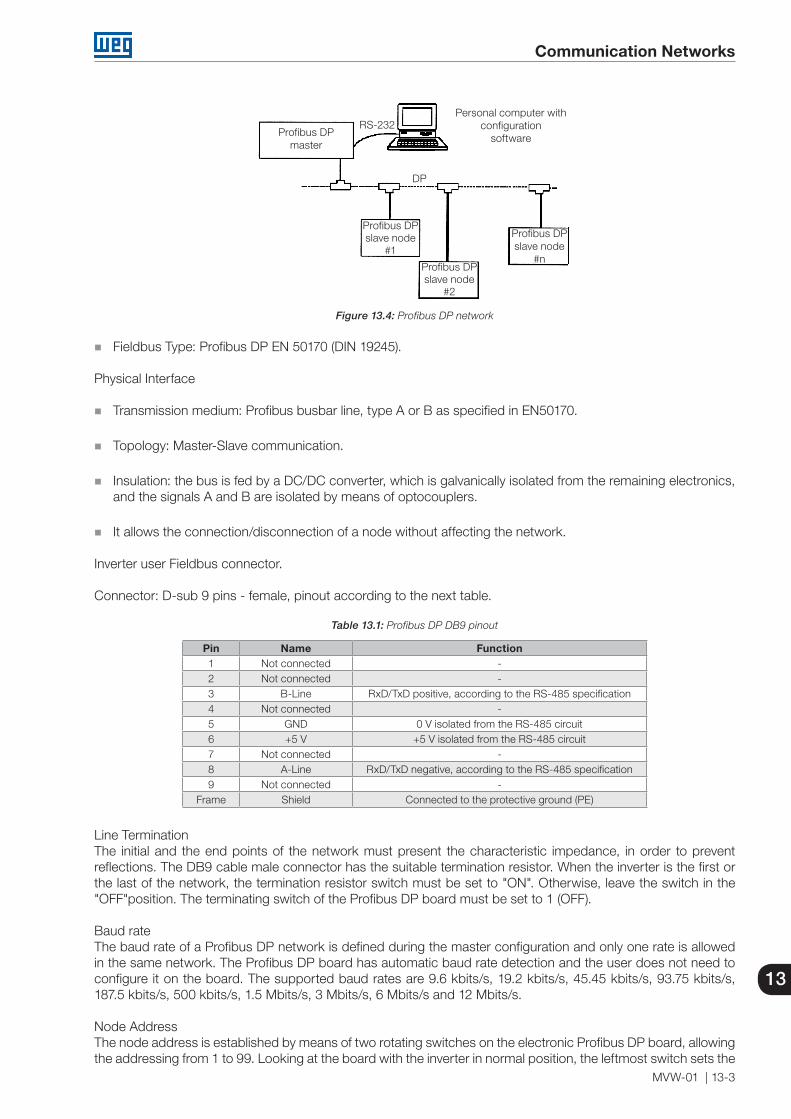
Communication Networks
MVW-01 | 13-3
13
Profibus DPmaster
Profibus DPslave node
#1
Profibus DPslave node
#2
Profibus DPslave node
#n
DP
RS-232Personal computer with
configurationsoftware
Figure 13.4: Profibus DP network
Fieldbus Type: Profibus DP EN 50170 (DIN 19245).
Physical Interface
Transmission medium: Profibus busbar line, type A or B as specified in EN50170.
Topology: Master-Slave communication.
Insulation: the bus is fed by a DC/DC converter, which is galvanically isolated from the remaining electronics, and the signals A and B are isolated by means of optocouplers.
It allows the connection/disconnection of a node without affecting the network.
Inverter user Fieldbus connector.
Connector: D-sub 9 pins - female, pinout according to the next table.
Table 13.1: Profibus DP DB9 pinout
Pin Name Function1 Not connected -2 Not connected -3 B-Line RxD/TxD positive, according to the RS-485 specification4 Not connected -5 GND 0 V isolated from the RS-485 circuit6 +5 V +5 V isolated from the RS-485 circuit7 Not connected -8 A-Line RxD/TxD negative, according to the RS-485 specification9 Not connected -
Frame Shield Connected to the protective ground (PE)
Line TerminationThe initial and the end points of the network must present the characteristic impedance, in order to prevent reflections. The DB9 cable male connector has the suitable termination resistor. When the inverter is the first or the last of the network, the termination resistor switch must be set to "ON". Otherwise, leave the switch in the "OFF"position. The terminating switch of the Profibus DP board must be set to 1 (OFF).
Baud rateThe baud rate of a Profibus DP network is defined during the master configuration and only one rate is allowed in the same network. The Profibus DP board has automatic baud rate detection and the user does not need to configure it on the board. The supported baud rates are 9.6 kbits/s, 19.2 kbits/s, 45.45 kbits/s, 93.75 kbits/s, 187.5 kbits/s, 500 kbits/s, 1.5 Mbits/s, 3 Mbits/s, 6 Mbits/s and 12 Mbits/s.
Node AddressThe node address is established by means of two rotating switches on the electronic Profibus DP board, allowing the addressing from 1 to 99. Looking at the board with the inverter in normal position, the leftmost switch sets the
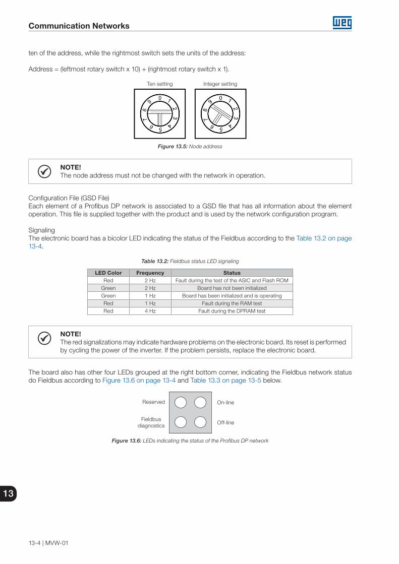
Communication Networks
13-4 | MVW-01
13
ten of the address, while the rightmost switch sets the units of the address:
Address = (leftmost rotary switch x 10) + (rightmost rotary switch x 1).
Ten setting Integer setting
Figure 13.5: Node address
NOTE!The node address must not be changed with the network in operation.
Configuration File (GSD File)Each element of a Profibus DP network is associated to a GSD file that has all information about the element operation. This file is supplied together with the product and is used by the network configuration program.
SignalingThe electronic board has a bicolor LED indicating the status of the Fieldbus according to the Table 13.2 on page 13-4.
Table 13.2: Fieldbus status LED signaling
LED Color Frequency StatusRed 2 Hz Fault during the test of the ASIC and Flash ROM
Green 2 Hz Board has not been initializedGreen 1 Hz Board has been initialized and is operatingRed 1 Hz Fault during the RAM testRed 4 Hz Fault during the DPRAM test
NOTE!The red signalizations may indicate hardware problems on the electronic board. Its reset is performed by cycling the power of the inverter. If the problem persists, replace the electronic board.
The board also has other four LEDs grouped at the right bottom corner, indicating the Fieldbus network status do Fieldbus according to Figure 13.6 on page 13-4 and Table 13.3 on page 13-5 below.
Reserved
Fieldbusdiagnostics
On-line
Off-line
Figure 13.6: LEDs indicating the status of the Profibus DP network

Communication Networks
MVW-01 | 13-5
13
Table 13.3: Profibus DP network status LEDs
LED Color Function
Fieldbusdiagnostics
Red
It indicates the following faults on the Fieldbus side:Flashing 1 Hz - Configuration error: the IN/OUT area size set at board initialization is different from the size set during the network configuration.Flashing 2 Hz - Error in the user parameter data: the size/content of the user parameter data set at board initialization is different from the size/content set during the network configuration.Flashing 4 Hz - Profibus Communication ASIC initialization error. OFF - No present problems.
On-line GreenIndicates that the board is on-line in Fieldbus network:ON - The board is on-line and the data exchange is possible.OFF - The board is not on-line.
Off-line RedIndicates that the board is off-line in Fieldbus network:ON - The board is off-line and the data exchange is not possible.OFF - The board is not off-line.
NOTE! When power is applied to the drive and both on-line and off-line LEDs on the Profibus DP board
flash alternately, then a network address configuration or an installation problem may be present. Check the installation and the network node address. Refer to the Item 13.1.6 Fieldbus Application/MVW-01 Related Parameters on page 13-7, for
DeviceNet application/MVW-01 related parameters.
13.1.3 DeviceNet
The DeviceNet communication is used for industrial automation, mainly for the control of valves, sensors, input/output units and automation equipment. The DeviceNet communication link is based on a communication protocol “broadcast oriented”, the Controller Area Network (CAN). The physical medium of the DeviceNet network consists of a shielded cable comprising a twisted pair and two wires for the external power supply. The baud rate can be set to 125 kbits/s, 250 kbits/s or 500 kbits/s. The Figure 13.7 on page 13-5 for Profibus DP application/MVW-01 related parameters.
Controller
Otherdevices
Deviceconfiguration Input/Output
devices
Motorstarter
DeviceNet
Sensor
Motor controller
Push buttoncluster
Bar code scanner
Drive
Figure 13.7: DeviceNet network
Inverter user Fieldbus connector.
5 pin plug-in terminal block (screw terminal), pinout according to the next table.
Table 13.4: DeviceNet terminal block pinout
Terminal Description Color1 V- Black2 CAN_L Blue3 Cable shield -4 CAN_H White5 V+ Red
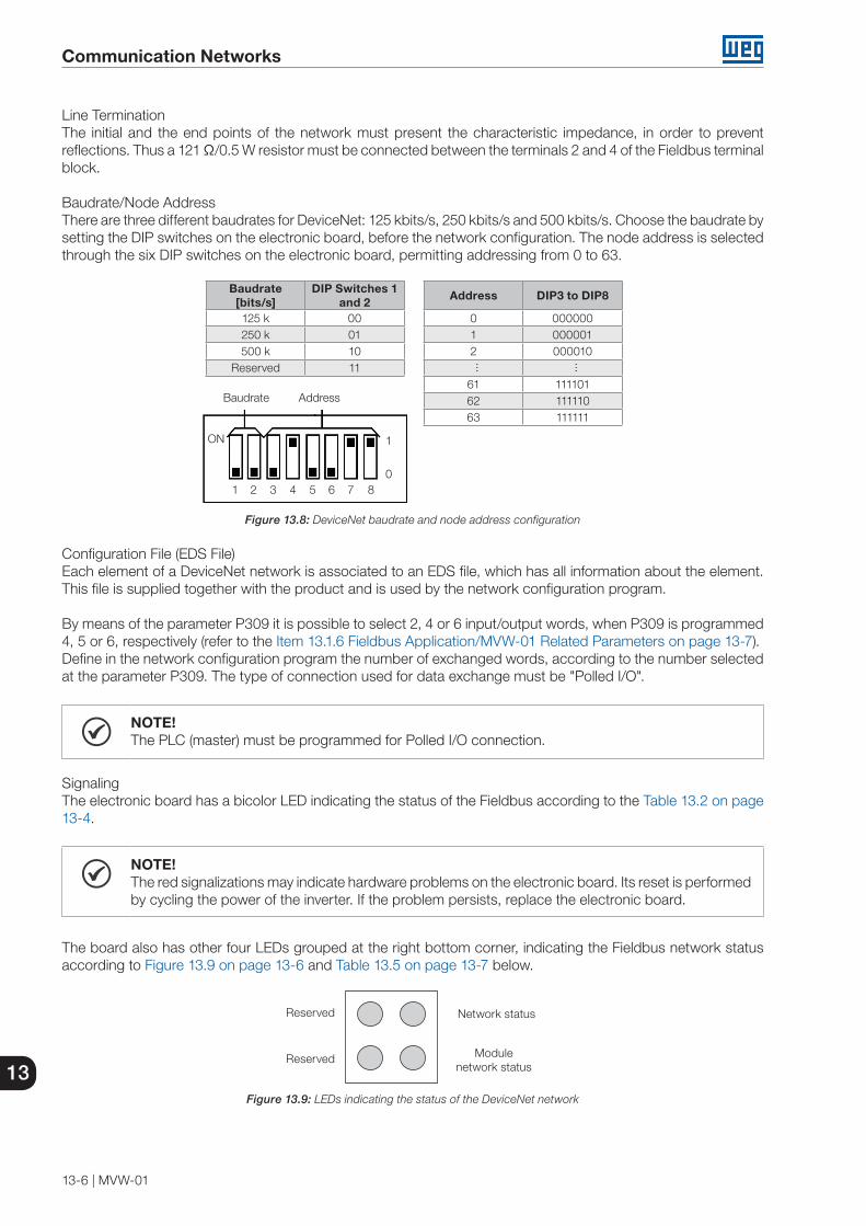
Communication Networks
13-6 | MVW-01
13
Line TerminationThe initial and the end points of the network must present the characteristic impedance, in order to prevent reflections. Thus a 121 Ω/0.5 W resistor must be connected between the terminals 2 and 4 of the Fieldbus terminal block.
Baudrate/Node AddressThere are three different baudrates for DeviceNet: 125 kbits/s, 250 kbits/s and 500 kbits/s. Choose the baudrate bysetting the DIP switches on the electronic board, before the network configuration. The node address is selectedthrough the six DIP switches on the electronic board, permitting addressing from 0 to 63.
Baudrate [bits/s]
DIP Switches 1and 2
125 k 00250 k 01500 k 10
Reserved 11
Address DIP3 to DIP8
0 0000001 0000012 000010
...
...
61 11110162 11111063 111111
AddressBaudrate
ON
1
1
02 3 4 5 6 7 8
Figure 13.8: DeviceNet baudrate and node address configuration
Configuration File (EDS File)Each element of a DeviceNet network is associated to an EDS file, which has all information about the element. This file is supplied together with the product and is used by the network configuration program.
By means of the parameter P309 it is possible to select 2, 4 or 6 input/output words, when P309 is programmed4, 5 or 6, respectively (refer to the Item 13.1.6 Fieldbus Application/MVW-01 Related Parameters on page 13-7).Define in the network configuration program the number of exchanged words, according to the number selectedat the parameter P309. The type of connection used for data exchange must be "Polled I/O".
NOTE!The PLC (master) must be programmed for Polled I/O connection.
SignalingThe electronic board has a bicolor LED indicating the status of the Fieldbus according to the Table 13.2 on page 13-4.
NOTE!The red signalizations may indicate hardware problems on the electronic board. Its reset is performed by cycling the power of the inverter. If the problem persists, replace the electronic board.
The board also has other four LEDs grouped at the right bottom corner, indicating the Fieldbus network status according to Figure 13.9 on page 13-6 and Table 13.5 on page 13-7 below.
Reserved Network status
Module network status
Reserved
Figure 13.9: LEDs indicating the status of the DeviceNet network
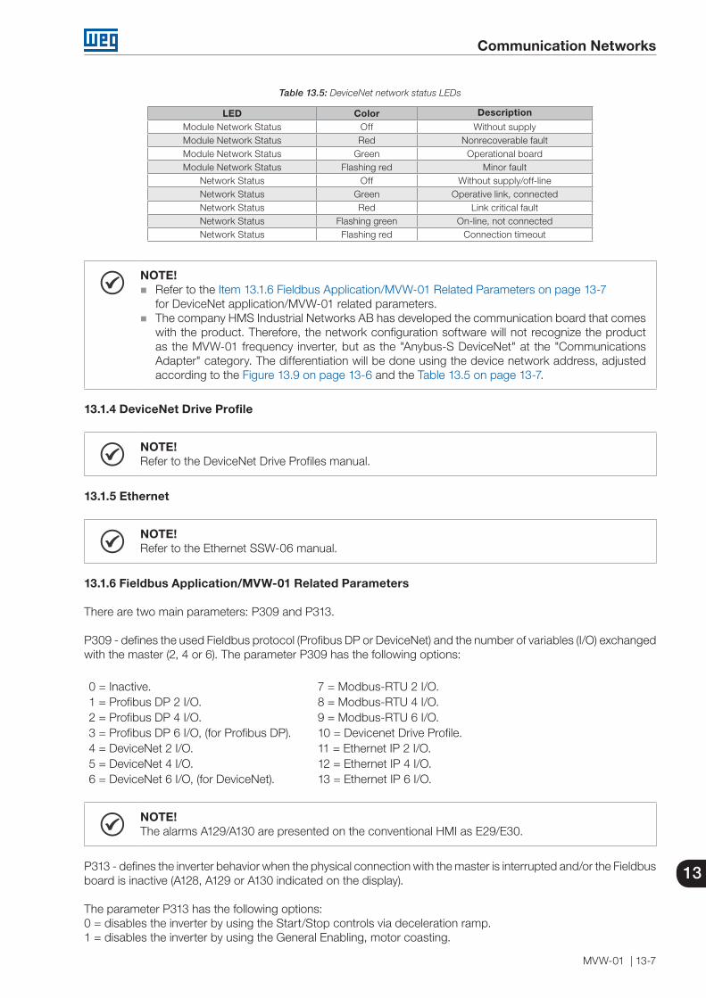
Communication Networks
MVW-01 | 13-7
13
Table 13.5: DeviceNet network status LEDs
LED Color Description
Module Network Status Off Without supplyModule Network Status Red Nonrecoverable faultModule Network Status Green Operational boardModule Network Status Flashing red Minor fault
Network Status Off Without supply/off-lineNetwork Status Green Operative link, connectedNetwork Status Red Link critical faultNetwork Status Flashing green On-line, not connectedNetwork Status Flashing red Connection timeout
NOTE! Refer to the Item 13.1.6 Fieldbus Application/MVW-01 Related Parameters on page 13-7
for DeviceNet application/MVW-01 related parameters. The company HMS Industrial Networks AB has developed the communication board that comes
with the product. Therefore, the network configuration software will not recognize the product as the MVW-01 frequency inverter, but as the "Anybus-S DeviceNet" at the "Communications Adapter" category. The differentiation will be done using the device network address, adjusted according to the Figure 13.9 on page 13-6 and the Table 13.5 on page 13-7.
13.1.4 DeviceNet Drive Profile
NOTE!Refer to the DeviceNet Drive Profiles manual.
13.1.5 Ethernet
NOTE!Refer to the Ethernet SSW-06 manual.
13.1.6 Fieldbus Application/MVW-01 Related Parameters
There are two main parameters: P309 and P313.
P309 - defines the used Fieldbus protocol (Profibus DP or DeviceNet) and the number of variables (I/O) exchangedwith the master (2, 4 or 6). The parameter P309 has the following options:
0 = Inactive.1 = Profibus DP 2 I/O.2 = Profibus DP 4 I/O.3 = Profibus DP 6 I/O, (for Profibus DP).4 = DeviceNet 2 I/O.5 = DeviceNet 4 I/O.6 = DeviceNet 6 I/O, (for DeviceNet).
7 = Modbus-RTU 2 I/O.8 = Modbus-RTU 4 I/O.9 = Modbus-RTU 6 I/O.10 = Devicenet Drive Profile.11 = Ethernet IP 2 I/O.12 = Ethernet IP 4 I/O.13 = Ethernet IP 6 I/O.
NOTE!The alarms A129/A130 are presented on the conventional HMI as E29/E30.
P313 - defines the inverter behavior when the physical connection with the master is interrupted and/or the Fieldbusboard is inactive (A128, A129 or A130 indicated on the display).
The parameter P313 has the following options:0 = disables the inverter by using the Start/Stop controls via deceleration ramp.1 = disables the inverter by using the General Enabling, motor coasting.
Communication Networks
13-8 | MVW-01
13
2 = the inverter status is not changed.3 = the inverter goes to Local mode.
13.1.6.1 Variables Read From the Inverter
1. Status word.2. Motor speed, for the option P309 = 1 or 4 (2I/O) - read 1 and 2.3. Digital input status (P012).4. Parameter contents, for the option P309 = 2 or 5 (4I/O) - read 1, 2, 3 and 4.5. Parameter contents, for the option (P009).6. Motor current (P003), for the option P309 = 3 or 6 (6I/O) - read 1, 2, 3, 4, 5 and 6.
1. Status word (EL):The status word is composed by a total of 16 bits, 8 high order bits and 8 low order bits. It has the following construction:
High-order bits - they indicate the status of the associated function.EL.15 - Active error: 0 = No, 1 = Yes.EL.14 - PID Regulator: 0 = Manual, 1 = Automatic.EL.13 - Undervoltage of the electronics power supplies: 0 = Without, 1 = With.EL.12 - Local/Remote command: 0 = Local, 1 = Remote.EL.11 - JOG command: 0 = Inactive, 1 = Active.EL.10 - Forward/Reverse: 0 = Reverse, 1 = Forward.EL.09 - General enabling: 0 = Disabled, 1 = Enabled.EL.08 * - Start/Stop: 0 = Stop, 1 = Start.(*) EL.08 = 1 means the inverter received the Run/Stop command via networks. This EL is not intended to signal that the motor is effectively spinning.
Low-order bits -they indicate the error code number, i.e., 03, 07 or 87 (57h).Refer to the Section 14.1 ALARMS/FAULTS AND POSSIBLE CAUSES on page 14-1.
2. Motor speed:This variable is shown by using 13-bit resolution plus signal. Thus, the rated value will be equal to 8191 (1FFFh) (Forward) or -8191 (E001h) (Reverse) when the motor is running at synchronous speed (or base speed, for instance 1800 rpm for a IV-pole motor, 60 Hz).
3. Digital input status:It presents the parameter P012 contents, where 1 indicates an active input and 0 indicates an inactive input. Refer to the Section 11.1 ACCESS AND READ ONLY PARAMETERS - P000 to P099 on page 11-1. The digital inputs are distributed in the manner in this WORD:Bit.7 - DI1 status. Bit.2 - DI6 status.Bit.6 - DI2 status. Bit.1 - DI7 status.Bit.5 - DI3 status. Bit.0 - DI8 status.Bit.4 - DI4 status. Bit.8 - DI9 status.Bit.3 - DI5 status. Bit.9 - DI10 status.
4. Parameter contents:This position allows reading the contents of inverter parameters, which are selected at the position 4 - Number of the parameters to be read - of the variables written in the inverter. The read values have the same order of magnitude of those described in the product manual or showed on the HMI. The values are read without the decimal point, if that is the case. Examples:a) HMI displays 12.3, the Fieldbus reading will be 123.b) HMI displays 0.246, the Fieldbus reading will be 246.
There are some parameters whose representation on the LED display can suppress the decimal position when the values are higher than 99.9. These parameters are P100, P101, P102, P103, P155, P156, P157, P158, P169 (for P202 < 3), P290 and P401.Example: Indication on the LED display: 130.Indication on the LCD : 130.0, Fieldbus reading is: 1300.

Communication Networks
MVW-01 | 13-9
13
The reading of the parameter P006 via Fieldbus has the meaning presented in the detailed parameter description - Chapter 11 DETAILED PARAMETER DESCRIPTION on page 11-1.
5. Torque current:This position indicates P009 parameter contents, without the decimal point. A low pass filter with a time constantof 0.5 s filters this variable.
6. Motor current:This position indicates P003 parameter contents, without the decimal point. A low pass filter with a time constantof 0.3 s filters this variable.
13.1.6.2 Variables Written in Inverter
The variables are written in the following order:1. Control Word.2. Motor speed reference, for the option P309 = 1 or 4 (2I/O) - it writes in 1 and 2.3. Status of the digital outputs.4. Number of the parameters to be read, for the option P309 = 2 or 5 (4I/O) - it writes in 1, 2, 3 and 4.5. Number of the parameter to be changed.6. Content of the parameter to be changed, selected in the previous position, for the option P309 = 3 or 6 (6I/O)
- it writes in 1, 2, 3, 4, 5 and 6.
1. Control word (C.L.):The control word is composed by a total of 16 bits, 8 high order bits and 8 low order bits. It has the following construction:
High-order bits - they select the functions to be controlled, when the correspondent bits are set to 1.CL.15 - Inverter fault reset.CL.14 - Without function.CL.13 - To save the changes of parameters P169/P170 in the EEPROM.CL.12 - Local/Remote command.CL.11 - Jog command.CL.10 - Forward/Reverse.CL.09 - General Enabling.CL.08 - Start/Stop.
Low-order bits - they determine the activation of the functions selected in the high-order bits,CL.7 - Inverter fault reset: every time it changes from 0 to 1 it causes an inverter reset, except for the errors (exceptA124, A125, A126 and A127);CL.6 - No function.CL.5 - To save P169/P170 in the EEPROM: 0 = to save, 1 = not to save.CL.4 - Local/Remote command: 0 = Local, 1 = Remote.CL.3 - Jog command: 0 = Inactive, 1 = Active.CL.2 - Forward/Reverse: 0 = Reverse, 1 = Forward.CL.1 - General enabling: 0 = Disabled, 1 = Enabled.CL.0 - Start/Stop: 0 = Stop, 1 = Start.
NOTE! The inverter will only execute the command defined in the low-order bit if the correspondent
high-order bit is set to 1 (one). If the high-order bit is set to 0 (zero), the inverter will disregard the value of the correspondent low-order bit.
CL.13: The function of saving parameter content changes in the EEPROM occurs normally when the HMI is used. The EEPROM allows a limited number of writings (100.000). In applications in which the speed regulator remains saturated and torque control is required, this control can be achieved by adjusting the torque limits P169/P170 (valid for P202 > 2). Therefore, if the network master keeps writing continuously in P169/P170, then the correspondent bits must be programmed in order to avoid that every change be saved in the EEPROM by setting: CL.13 = 1 and CL.5 = 1.
In order to enable the functions of the Control Word, it is necessary to set the inverter respective parameters withthe option "Fieldbus".
Communication Networks
13-10 | MVW-01
13
a) Local/Remote Selection Source - P220.b) Speed Reference - P221 and/or P222.c) Forward/Reverse Selection - P223 and/or P226.d) General Enabling, Start/Stop Selection - P224 and/or P227.e) JOG Selection - P225 and/or P228.
2. Motor speed reference:This variable is presented using a 13 bit resolution. Therefore, the speed reference value for the motor synchronousspeed will be equal to 8191 (1FFFh).This value must be used only as the base speed for the calculation of the desired speed (speed reference).
Examples:1. 4-pole, 60 Hz motor, synchronous speed = 1800 rpm and speed reference = 650 rpm.
1800 rpm - 8191 650 rpm - X X = 2958 = 0B8Eh
This value (0B8Eh) must be written in the second word, which represents the motor speed reference (accordingto the beginning of this item.).
2. 6-pole, 60 Hz motor, synchronous speed = 1200 rpm and speed reference = 1000 rpm.
1200 rpm - 8191 1000 rpm - X X = 4096 = 1AAAh
This value (1AAAh) must be written in the second word, which represents the motor speed reference (accordingto the beginning of this item).
NOTE!Values above 8191 (1FFFh) are allowed when speed references above the motor synchronous speedare required, as long as the maximum programmed speed reference is respected.
3. Status of the digital outputs: It allows controlling the status of the digital outputs that have been programmed for Fieldbus at the parameters P275 to P282. 16 bits, with the following construction, form the word that defines the status of the digital outputs:
High-order bits: they define the outputs to be controlled, when set in 1.Bit.08: 1 - DO1 output control.Bit.09: 1 - DO2 output control.Bit.10: 1 - RL1 output control.Bit.11: 1 - RL2 output control.Bit.12: 1 - RL3 output control.
Low-order bits: they define the status of the controlled outputs.Bit.0 - DO1 status: 0 = inactive output, 1 = active output.Bit.1 - DO2 status: idem.Bit.2 - RL1 status: idem.Bit.3 - RL2 status: idem.Bit.4 - RL3 status: idem.
4. Number of the parameters to be read:Through this position, the reading of any inverter parameter can be defined. The number of the parameter to be read must be programmed here, and its contents will be presented at the position 4 of the variables read from the inverter.
5. Number of the parameter to be changed: (parameter contents modification).This position operates together with the position 6, described next.When no parameter has to be changed, then fill this position with the code 999.
Communication Networks
MVW-01 | 13-11
13
Changing process sequence:
- Keep 999 in the position 5.
- Replace 999 by the number of the parameter to be changed.
- If no error code (124 to 127) is signalized in the Status Word, then replace the parameter number by 999, in order to conclude the modification.
The modification can be verified via the HMI or by reading the parameter contents.
NOTE!1. The command to pass from V/F to vector control will not be accepted if any of the parameters from
P409 to P413 remains set to zero. In such case, this command must be done via HMI.2. Do not program P204 = 5, because in the factory default settings P309 = Inactive.3. P204 and P408 do not accept modification via network command.4. The parameter contents must be kept by the master during 15.0 ms. Send a new value or write in another parameter only after this time has elapsed.
6. Content of the parameter to be changed, selected at the position 5: (Number of the parameter to be changed) The format of the values adjusted in this position must be the ones described in the manual. The values, however, must be written without the decimal point, if this is the case. When the parameters P409 to P413 are modified, small differences in the contents may occur when comparing the value sent via Fieldbus and the value read at the position 4. (Parameter contents) or at the HMI, because of the truncating during the reading process.
13.1.6.3 Error Indications
During the Fieldbus reading/writing process the following error indications may occur and be informed at theStatus Word variable:
Status Word variable indications:A124 - An attempt to change a parameter that can be modified only with disabled inverter. - Parameterization error.A125 - Caused by: - Reading of non-existent parameter, or - Writing on non-existent parameter, or - Writing on P408 and P204.A126 - An attempt to write a value out of the permitted range.A127 - Caused by: a) A function selected by the Control Word has not been programmed for Fieldbus, or b) Command of a digital output that has not been programmed for Fieldbus, or c) An attempt to write in a read-only parameter.
The indication of the listed errors will be removed from the Status Word when the indented action is sent correctly,except for A127 (“b” case), whose reset is performed writing in the Control Word.
Example: Assuming that no digital output has been programmed for Fieldbus, then if the word 11h is written in the position 3, the inverter will respond indicating A127 in the Status Word. To remove this indication from the Status Word it is necessary: 1. To write zero in the position 3 (because no DO has been programmed for Fieldbus).
2. To change the Control Word variable so that the A127 indication be removed from the Status Word.
The removal of the listed errors from the Status Word can also be achieved by writing the 999 code in the position5 of the variables written in the inverter. Except for A127 (“b” and “a” cases), whose reset occurs only through thewriting in the Control Word, as exemplified above.
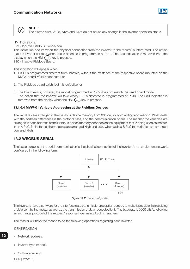
Communication Networks
13-12 | MVW-01
13
NOTE!The alarms A124, A125, A126 and A127 do not cause any change in the inverter operation status.
HMI Indications:E29 - Inactive Fieldbus ConnectionThis indication occurs when the physical connection from the inverter to the master is interrupted. The action that the inverter will take when E29 is detected is programmed at P313. The E29 indication is removed from the display when the HMI key is pressed.E30 - Inactive Fieldbus Board.
This indication will appear when:1. P309 is programmed different from Inactive, without the existence of the respective board mounted on the
MVC4 board XC140 connector, or
2. The Fieldbus board exists but it is defective, or
3. The board exists; however, the model programmed in P309 does not match the used board model. The action that the inverter will take when E30 is detected is programmed at P313. The E30 indication is
removed from the display when the HMI key is pressed.
13.1.6.4 MVW-01 Variable Addressing at the Fieldbus Devices
The variables are arranged in the Fieldbus device memory from 00h on, for both writing and reading. What deals with the address differences is the protocol itself, and the communication board. The manner the variables are arranged in each address of the Fieldbus device memory depends on the equipment that is being used as master. In an A PLC, for instance, the variables are arranged High and Low, whereas in a B PLC the variables are arranged Low and High.
13.2 WEGBUS SERIAL
The basic purpose of the serial communication is the physical connection of the inverters in an equipment networkconfigured in the following form:
Master PC, PLC, etc.
Slave 1(Inverter)
Slave 2(Inverter)
Slave n(Inverter)
n ≤ 30
Figure 13.10: Serial configuration
The inverters have a software for the interface data transmission/reception control, to make it possible the receiving of data sent by the master as well as the transmission of data requested by it. The baudrate is 9600 bits/s, following an exchange protocol of the request/response type, using ASCII characters.
The master will have the means to do the following operations regarding each inverter:
IDENTIFICATION
Network address.
Inverter type (model).
Software version.
Communication Networks
MVW-01 | 13-13
13
COMMAND
General enabling/disabling.
Enable/Disable by ramp (Run/Stop).
Speed direction.
Speed reference.
Local/Remote.
JOG.
Fault RESET.
STATUS ACKNOWLEDGMENT
Ready.
Sub.
Run.
Local/Remote.
Fault.
JOG.
Speed direction.
Setting mode after the reset to the factory default.
Setting mode after changing from V/F mode to Vector mode.
PARAMETER READING
PARAMETER MODIFICATION
Typical examples of network use:
PC (master) for parameterization of one or several inverters at the same time.
SDCD monitoring inverter variables.
PLC controlling the operation of an inverter in an industrial process.
Description of the InterfacesThe physical connection between the inverters and the network master is performed according to one of the standards below:a) RS-232 (point-to-point, up to 10 m).b) RS-485 (multipoint, galvanic isolation, up to 1000 m).
RS-485This interface allows the connection of up to 30 inverters to a master (PC, PLC, etc.), attributing to each inverter an address (1 to 30) that must be set at each one. In addition to these 30 addresses, there are two other addresses available to perform special tasks:Address 0: any inverter in the network is inquired, regardless of its address. Only one inverter must be connectedto the network (point-to-point) in order to prevent short-circuits in the interface lines.
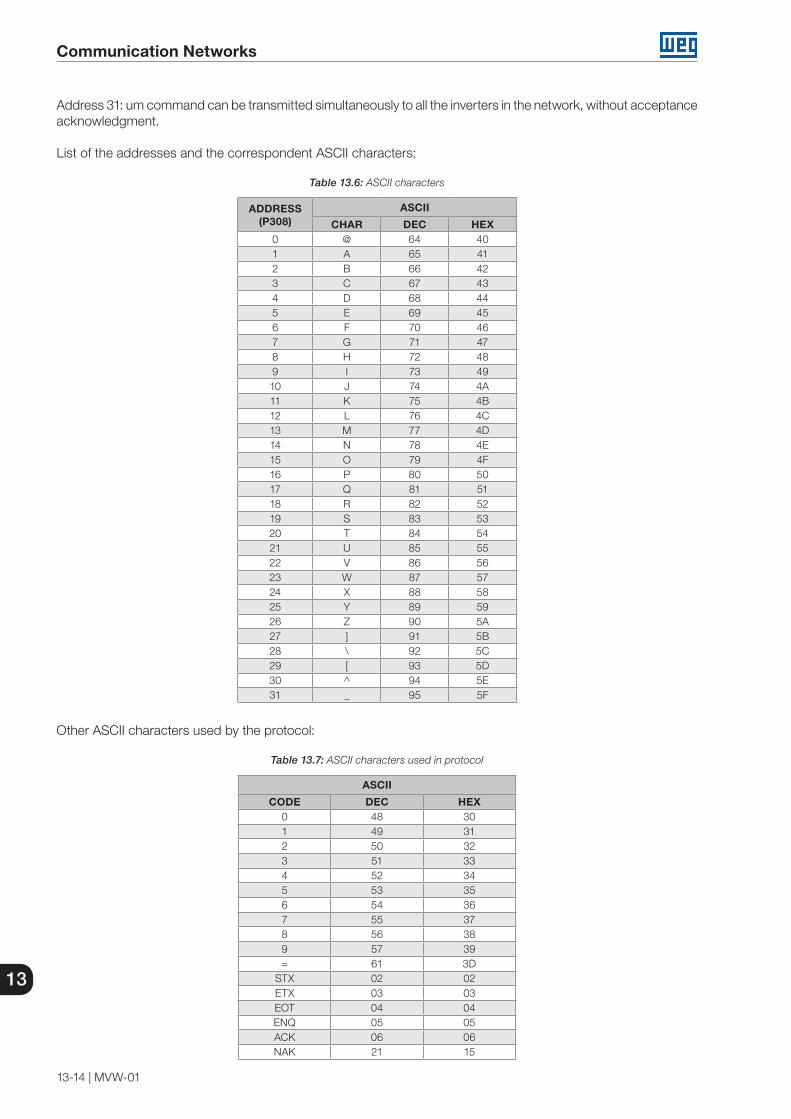
Communication Networks
13-14 | MVW-01
13
Address 31: um command can be transmitted simultaneously to all the inverters in the network, without acceptanceacknowledgment.
List of the addresses and the correspondent ASCII characters:
Table 13.6: ASCII characters
ADDRESS(P308)
ASCII
CHAR DEC HEX0 @ 64 401 A 65 412 B 66 423 C 67 434 D 68 445 E 69 456 F 70 467 G 71 478 H 72 489 I 73 4910 J 74 4A11 K 75 4B12 L 76 4C13 M 77 4D14 N 78 4E15 O 79 4F16 P 80 5017 Q 81 5118 R 82 5219 S 83 5320 T 84 5421 U 85 5522 V 86 5623 W 87 5724 X 88 5825 Y 89 5926 Z 90 5A27 ] 91 5B28 \ 92 5C29 [ 93 5D30 ^ 94 5E31 _ 95 5F
Other ASCII characters used by the protocol:
Table 13.7: ASCII characters used in protocol
ASCII
CODE DEC HEX0 48 301 49 312 50 323 51 334 52 345 53 356 54 367 55 378 56 389 57 39= 61 3D
STX 02 02ETX 03 03EOT 04 04ENQ 05 05ACK 06 06NAK 21 15

Communication Networks
MVW-01 | 13-15
13
The connection between the network nodes is performed through a pair of wires. The signal levels are according to RS-485 EIA STANDARD, with differential receivers and transmitters. Expansion boards EBA.01, EBA.02 or EBB.01 (refer to Item 10.2.1 EBA (I/O Expansion Board A) on page 10-5 and the Item 10.2.2 EBB (I/O Expansion Board B) on page 10-8).
When the master does only have a RS-232 interface, then a RS232/RS485 converter must be used.
RS-232With the RS-232 interface the connection of one master to one slave is possible (point-to-point). Data can be exchanged in a bidirectional way, but not simultaneously (HALF DUPLEX).
The logic levels follow the RS-232 EIA STANDARD, which determines the use of unbalanced signaling. In the present case, one wire is used for transmission (TX), other for reception (RX) and another for ground (0 V). This configuration is the minimal “3-wire” RS-232 connection (3-wire economy model).Note: refer to the Item 13.2.4 RS-232 and RS-485 Physical Connection on page 13-22 which describes the physical connection.
13.2.1 Protocol Definitions
Used Terms
Parameters: Are those existent in the inverter, whose visualization or modification is possible through the HMI.
Variables: are values with specific functions in the inverter and can be read and, in some cases, modified by the master.
Basic Variables: Are those that can only be accessed through the serial communication.
Diagram:
Inverter
Basic variables
Parameters
MasterSerial connection
Variables
Figure 13.11: Scheme of basic variables
Parameter/Variable ResolutionsDuring parameter reading/writing their decimal points are disregarded in the values received/sent via telegrams,whereas the basic variables V04 (Serial Reference) and V08 (Motor Speed) that are standardized as 13 bit (0 to 8191).
Examples:
Writing: If the purpose is to change the P100 content to 10.0 s, 100 must be sent (disregarding the decimal point).
Reading: If 1387 (disregarding the decimal point) is read from P409, them its value is 1.387.
Writing: in order to change V04 content to 900 rpm one must send:
V04 = 900 x 8191 = 4096 P208
Assuming that P208 = 1800 rpm
Reading: If 1242 is read from V08, the corresponding value is given by:
V08 = 1242 x P208 = 273 rpm 8191

Communication Networks
13-16 | MVW-01
13
Assuming that P208 = 1800 rpm
Character Format 1 start bit.
8 data bits (they codify text and transmission characters, taken from the 7-bit code, according to ISO 646 and complemented for even parity [eighth bit]).
1 stop bit.
After the start bit goes the least significant bit:
START B1 B2 B3 B4 B5 B6 B7 B8 STOP
Startbit
Stopbit8 data bits
13.2.2 Variable Code
V00 (code 00800):Inverter model indication (reading variable). The reading of this variable allows identifiying the inverter type. For the MVW-01, this value is 8, as follows:
CODE X X X X X
Number of the basic variable or parameter
Equipment number:"8" = MVW-01"9" = any inverter
Specifier:0 = basic variables1 = P000 to P0992 = P100 to P1993 = P200 to P2994 = P300 to P3995 = P400 to P4996 = P500 to P5997 = P600 to P699
Equal to zero (0)
V02 (code 00802):Inverter status indication (reading variable).
Status word (byte-high).
Error code (byte-low).
Where:Status Word:
EL15 EL14 EL13 EL12 EL11 EL10 EL9 EL8
EL8: 0 = Enable by ramp (run/stop) inactive / 1 = Enable by ramp active.
EL9: 0 = General enable inactive / 1 = General enable active.
EL10: 0 = Reverse / 1 = Forward.
EL11: 0 = JOG inactive / 1 = JOG active.

Communication Networks
MVW-01 | 13-17
13
EL12: 0 = Local / 1 = Remote.
EL13: 0 = Without undervoltage / 1 = With undervoltage.
EL14: 0 = Manual (PID) / 1 = Automatic (PID).
EL15: 0 = Without fault / 1 = With fault.
Error code: error number in hexadecimal format.Examples: F001 → 01hF087 → 57h
V03 (code 00803):Selection of logical command.Writing variable, whose bits have the following meaning:
High-order bits: desired action mask. In order that the action be possible, the correspondent bit must be set in 1.
CL15 CL14 CL13 CL12 CL11 CL10 CL9 CL8
MSB LSB
CL8: 1 = Enable ramp (run/stop).
CL9: 1 = General Enable.
CL10: 1 = Forward/Reverse.
CL11: 1 = JOG.
CL12: 1 = Local/Remote.
CL13: Not used.
CL14: Not used.
CL15: 1 = Inverter "RESET".
Low-order bit: logic level of the desired action.
CL7 CL6 CL5 CL4 CL3 CL2 CL1 CL0
MSB LSB
CL0: 1 = Enable (run) / 0 = Disable by ramp (stop).
CL1: 1 = Enable / 0 = General disable (stop by inertia).
CL2: 1 = Forward / 0 = Reverse.
CL3: 1 = JOG active / 0 = JOG inactive.
CL4: 1 = Remote / 0 = Local.
CL5: Not used.
CL6: Not used.
CL7: Transition from 0 to 1 in this bit "RESETS" the inverter in case it is in some fault condition.

Communication Networks
13-18 | MVW-01
13
NOTE! A disable command via digital input has higher priority than the Control Word enabling. In order to enable the inverter it is necessary that CL0 = CL1 = 1, and that there is no external
disabling command. If CL0 and CL1 are set to 0 simultaneously, than general disable occurs.
V04 (code 00804):Serial speed reference (reading/writing variable).It allows sending the speed reference to the inverter, as long as P221 = 9 for Local situation, or P222 = 9 for Remote situation. This variable has a 13 bit resolution (refer to the Item 13.2.1 Protocol Definitions on page 13-15).
V06 (code 00806):Status of the operation modes (reading variable).
EL2 EL2 EL2 EL2 EL2 EL2 EL2 EL2 7 6 5 4 3 2 1 0
MSB LSB
EL2.0: 1 = during the Guided Start-up Routine after a reset to the factory default/first power-up.
The inverter will enter this operation mode when it is powered-up for the first time or when the factory default parameters are loaded (P204 = 5 or 6). In this mode only the parameters P023, P201, P295, P296, P400, P401, P402, P403, P404 and P406 will be accessible. If an attempt to access another parameter is done, the inverter will respond with A125. In order to get more details, refer to the Item 8.3.2 Initial Power-up (Parameter Settings) on page 8-18.
EL2.1: 1 = during the adjusting mode after changing from V/F to Vector Mode.
The inverter will enter this operation mode when the control mode is changed from V/F (P202 = 0, 1 or 2) to Vector (P202 = 3 or 4). In this mode only the parameters P023, P201, P295, P296, P400, P401, P402, P403, P404 and P406 will be accessible. If an attempt to access another parameter is done, the inverter will respond with A125.
EL2.2: 1 = performing the self-tuning.
EL2.3: not used.
EL2.4: not used.
EL2.5: not used.
EL2.6: not used.
EL2.7: not used.
V07 (code 00807):Status of the operation modes (reading/writing variable).
CL2 CL2 CL2 CL2 CL2 CL2 CL2 CL2 7 6 5 4 3 2 1 0
MSB LSB
CL2.0: 1 - it leaves the Guided Start-up Routine after a reset to the factory default.
CL2.1: 1 - it leaves the adjusting mode after changing from V/F to Vector Mode.
CL2.2: 1 - it aborts the self-tuning.
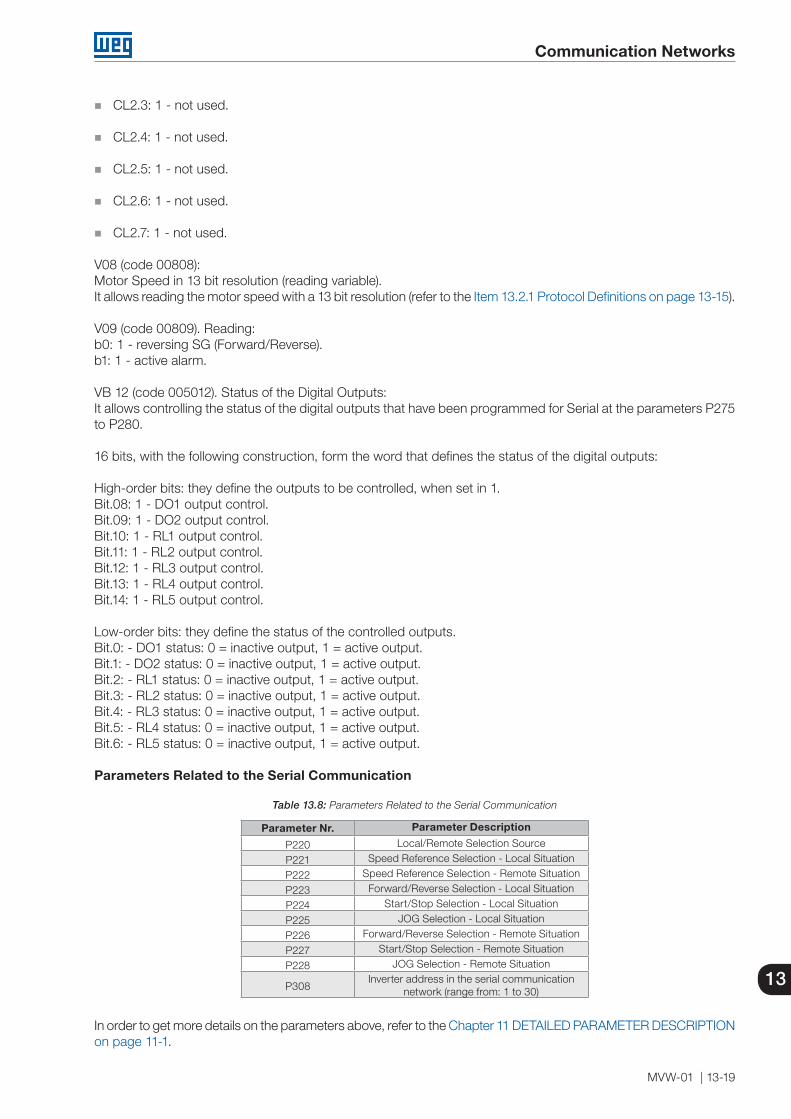
Communication Networks
MVW-01 | 13-19
13
CL2.3: 1 - not used.
CL2.4: 1 - not used.
CL2.5: 1 - not used.
CL2.6: 1 - not used.
CL2.7: 1 - not used.
V08 (code 00808):Motor Speed in 13 bit resolution (reading variable).It allows reading the motor speed with a 13 bit resolution (refer to the Item 13.2.1 Protocol Definitions on page 13-15).
V09 (code 00809). Reading:b0: 1 - reversing SG (Forward/Reverse).b1: 1 - active alarm.
VB 12 (code 005012). Status of the Digital Outputs:It allows controlling the status of the digital outputs that have been programmed for Serial at the parameters P275to P280.
16 bits, with the following construction, form the word that defines the status of the digital outputs:
High-order bits: they define the outputs to be controlled, when set in 1.Bit.08: 1 - DO1 output control.Bit.09: 1 - DO2 output control.Bit.10: 1 - RL1 output control.Bit.11: 1 - RL2 output control.Bit.12: 1 - RL3 output control.Bit.13: 1 - RL4 output control.Bit.14: 1 - RL5 output control.
Low-order bits: they define the status of the controlled outputs.Bit.0: - DO1 status: 0 = inactive output, 1 = active output.Bit.1: - DO2 status: 0 = inactive output, 1 = active output.Bit.2: - RL1 status: 0 = inactive output, 1 = active output.Bit.3: - RL2 status: 0 = inactive output, 1 = active output.Bit.4: - RL3 status: 0 = inactive output, 1 = active output.Bit.5: - RL4 status: 0 = inactive output, 1 = active output.Bit.6: - RL5 status: 0 = inactive output, 1 = active output.
Parameters Related to the Serial Communication
Table 13.8: Parameters Related to the Serial Communication
Parameter Nr. Parameter Description
P220 Local/Remote Selection Source
P221 Speed Reference Selection - Local Situation
P222 Speed Reference Selection - Remote Situation
P223 Forward/Reverse Selection - Local Situation
P224 Start/Stop Selection - Local Situation
P225 JOG Selection - Local Situation
P226 Forward/Reverse Selection - Remote Situation
P227 Start/Stop Selection - Remote Situation
P228 JOG Selection - Remote Situation
P308Inverter address in the serial communication
network (range from: 1 to 30)
In order to get more details on the parameters above, refer to the Chapter 11 DETAILED PARAMETER DESCRIPTION on page 11-1.

Communication Networks
13-20 | MVW-01
13
Errors Related to the Serial Communication
They operate in the following way:
The do not disable the inverter.
They do not commutate fault relays.
They are reported in the Status Word (V02).
Type of errors:
A122: longitudinal parity error (BCC).
A124: parameterization error (occurrence of some of the situations indicated in the Table 9.5 on page 9-10 or when there is an attempt to change a parameter that cannot be changed with a rotating motor).
A125: nonexistent variable or parameter.
A126: value out of the range.
A127: an attempt to write in a read-only variable or a disabled control word command.
NOTE! If in the inverter data reception a parity error is detected, then the telegram is ignored. The same
will happen in cases of syntax errors. Examples: Code values different from the numbers 0 to 9. Separation character different from " = ", etc.
13.2.3 MVW-01 Special Parameters
In general, the parameters of an inverter store their information in 16-bit words. To know the contents of one of these parameters through a communication network (serial, fieldbus, etc.), the number of the parameter must be informed (according to the used protocol) and a 16-bit information will be received as the answer, because there is only one information word associated for each parameter.
Some of the MVW-01 parameters have more than one word of associated information, so that the access to these parameters is done in a special manner. These parameters are:
Parameters of the last errors: P014 to P017, P060 to P065 - 3 words per parameter.
Date and Time: P080 and P081 - 2 words per parameter.
Error log: P067 - 300 words.
Trace function data: P555, P557, P559, P561, P563, P565, P567, P569 – up to 31080 words per parameter.
To gain access to the contents of these special parameters, successive readings must be performed until all the words associated to that parameter have been obtained (the readings must be done normally, according to the specified protocol), remembering that in each reading the access to only one word (16 bits) is obtained.
Communication Networks
MVW-01 | 13-21
13
NOTE!While reading special parameters, this reading should be done in an uninterrupted form, reading the same parameter repeated times without reading any other parameter in between until all the readings of the special parameter associated words have been accomplished. If another parameter is read before the conclusion of the reading of all the words, then when it is read again it sends the first associated word again.
Parameters of the Last ErrorsThe parameters that bring the information of the 10 last errors (P014 to P017, P060 to P065) have three words associated to each one of them.The first read word brings the information of the occurred error number and of the inverter status at the momentit occurred. The information is distributed among the word bits in the following way:
Status Error number
b15 b14 b13 b12 b11 b10 b9 b8 b7 b6 b5 b4 b3 b2 b1 b0
The second and the third words bring the information of the date/time when the error happened. The date/timeinformation has 32 bits and two words are necessary to represent it.In order to decode the date/time information, refer to the Item 13.2.1 Protocol Definitions on page 13-15.For instance, in order to obtain the information of the last error (P014 = read P014 three consecutive times.
Date and Time Parameters.The MVW-01 inverter has a real time clock with the purpose of recording date and time of events as, for instance,the occurred errors. Date and time can be adjusted through the parameters P080 and P081, respectively.
NOTE!Date and time can only be modified through the local HMI.
Despite having two parameters related with the date and hour, the information is stored in a single 32-bit variable. Thus, to obtain the inverter date and time information, two readings of P080 are necessary, since the informationis stored in 32 bits, i.e., in two words.
In the first reading the inverter sends the most significant word (bits 16 to 31) and in the second reading the less significant word (bits 0 to 15).
Those 32 bits of information contain the counting of the seconds elapsed since 00:00 a.m. of January 1st, 1970.A Julian codifying routine must be used to determine the date and the hour correspondent the this counting.
Error Log Parameter.The parameter P067 has the information of the 100 last inverter errors. Since each error has 3 words (48 bits) ofassociated information, this parameter has 300 words.
Therefore, the first three readings of P067 supply the information of the last error, the three following readings ofthe next one, and so on until 300 readings are done. For information on the words related to an error, refer to the Item 13.2.1 Protocol Definitions on page 13-15.
Trace Function Data Parameters.The trace function stores an enormous amount of information in each of its channels. To get access to this data, it is necessary to read the parameter related to the wanted channel (P555, P557, P559, P561, P563, P565, P567, P569).
When the first reading of a certain channel parameter is done, it responds with the number of the correspondingparameter programmed for trace.
Starting from the second reading on (in sequence), the information recorded by the trace function is sent.In order to know how many words are associated to each channel, refer to the Section 12.1 Trace Function on page 12-1.

Communication Networks
13-22 | MVW-01
13
Times for Telegram Reading/Writing.
MASTER Tx: (data)
RSND (request to send
INVERTER
TxD: (data)
tproctdi ttxi
Figure 13.12: Time of the telegrams exchanged between Master and Inverter
Table 13.9: Reading and writing time
Time Typical (ms)
Tproc 10Tdi 5
Ttxi
Reading 15Writing 3
13.2.4 RS-232 and RS-485 Physical Connection
Network master(PC,CLP)
MVW-01
Cable shield
A B 11 12
AB
XC4(EBA)
A
XC5(EBB)
B
AB
XC4(EBA)
A
XC5(EBB)
B
MVW-01 MVW-01
Cable shield
A B 11 12
Figure 13.13: Connection Scheme
Notes:
LINE TERMINATION: add a line termination (120 Ω) at the ends, and only at the ends, of the line. Therefore, set S3.1/S3.2 (EBA) and S7.1/S7.2 (EBB) in the on position (refer to the Item 10.2.1 EBA (I/O Expansion Board A) on page 10-5 and Item 10.2.2 EBB (I/O Expansion Board B) on page 10-8).
CABLE SHIELD GROUNDING: connect them to the equipment frames (properly grounded).
RECOMMENDED CABLE: balanced pair, shielded.
E.g., AFS Line, manufacturer KMP.
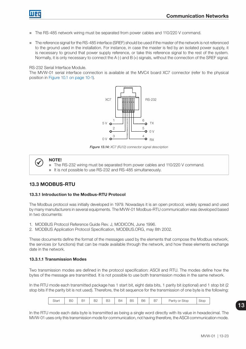
Communication Networks
MVW-01 | 13-23
13
The RS-485 network wiring must be separated from power cables and 110/220 V command.
The reference signal for the RS-485 interface (SREF) should be used if the master of the network is not referenced to the ground used in the installation. For instance, in case the master is fed by an isolated power supply, it is necessary to ground that power supply reference, or take this reference signal to the rest of the system. Normally, it is only necessary to connect the A (-) and B (+) signals, without the connection of the SREF signal.
RS-232 Serial Interface Module.The MVW-01 serial interface connection is available at the MVC4 board XC7 connector (refer to the physical position in Figure 10.1 on page 10-1).
XC7 RS-232
6
5
4
1
2
3
TX
0 V
RX
5 V
0 V
Figure 13.14: XC7 (RJ12) connector signal description
NOTE! The RS-232 wiring must be separated from power cables and 110/220 V command. It is not possible to use RS-232 and RS-485 simultaneously.
13.3 MODBUS-RTU
13.3.1 Introduction to the Modbus-RTU Protocol
The Modbus protocol was initially developed in 1979. Nowadays it is an open protocol, widely spread and used by many manufacturers in several equipments. The MVW-01 Modbus-RTU communication was developed based in two documents:
1. MODBUS Protocol Reference Guide Rev. J, MODICON, June 1996.2. MODBUS Application Protocol Specification, MODBUS.ORG, may 8th 2002.
These documents define the format of the messages used by the elements that compose the Modbus network, the services (or functions) that can be made available through the network, and how these elements exchange date in the network.
13.3.1.1 Transmission Modes
Two transmission modes are defined in the protocol specification: ASCII and RTU. The modes define how the bytes of the message are transmitted. It is not possible to use both transmission modes in the same network.
In the RTU mode each transmitted package has 1 start bit, eight data bits, 1 parity bit (optional) and 1 stop bit (2 stop bits if the parity bit is not used). Therefore, the bit sequence for the transmission of one byte is the following:
Start B0 B1 B2 B3 B4 B5 B6 B7 Parity or Stop Stop
In the RTU mode each data byte is transmitted as being a single word directly with its value in hexadecimal. TheMVW-01 uses only this transmission mode for communication, not having therefore, the ASCII communication mode.
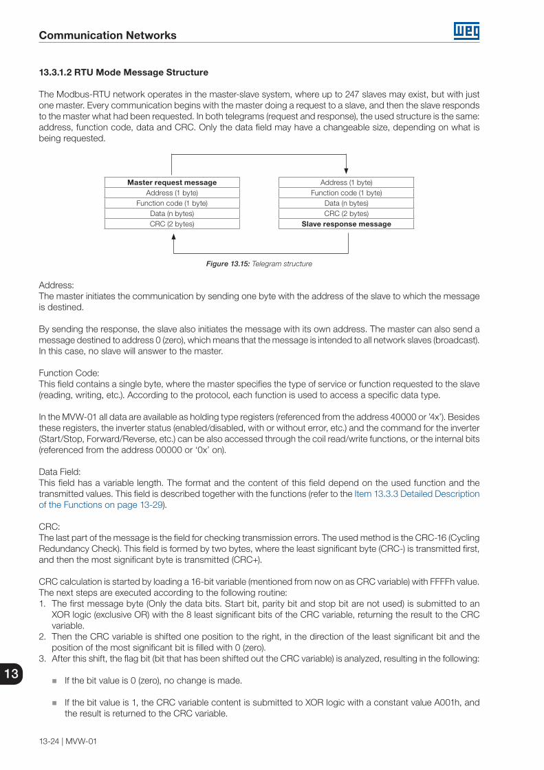
Communication Networks
13-24 | MVW-01
13
13.3.1.2 RTU Mode Message Structure
The Modbus-RTU network operates in the master-slave system, where up to 247 slaves may exist, but with just one master. Every communication begins with the master doing a request to a slave, and then the slave responds to the master what had been requested. In both telegrams (request and response), the used structure is the same: address, function code, data and CRC. Only the data field may have a changeable size, depending on what is being requested.
Master request messageAddress (1 byte)
Function code (1 byte)Data (n bytes)CRC (2 bytes)
Address (1 byte)Function code (1 byte)
Data (n bytes)CRC (2 bytes)
Slave response message
Figure 13.15: Telegram structure
Address:The master initiates the communication by sending one byte with the address of the slave to which the messageis destined.
By sending the response, the slave also initiates the message with its own address. The master can also send amessage destined to address 0 (zero), which means that the message is intended to all network slaves (broadcast).In this case, no slave will answer to the master.
Function Code:This field contains a single byte, where the master specifies the type of service or function requested to the slave(reading, writing, etc.). According to the protocol, each function is used to access a specific data type.
In the MVW-01 all data are available as holding type registers (referenced from the address 40000 or ’4x’). Besidesthese registers, the inverter status (enabled/disabled, with or without error, etc.) and the command for the inverter(Start/Stop, Forward/Reverse, etc.) can be also accessed through the coil read/write functions, or the internal bits(referenced from the address 00000 or ‘0x’ on).
Data Field:This field has a variable length. The format and the content of this field depend on the used function and the transmitted values. This field is described together with the functions (refer to the Item 13.3.3 Detailed Description of the Functions on page 13-29).
CRC:The last part of the message is the field for checking transmission errors. The used method is the CRC-16 (CyclingRedundancy Check). This field is formed by two bytes, where the least significant byte (CRC-) is transmitted first,and then the most significant byte is transmitted (CRC+).
CRC calculation is started by loading a 16-bit variable (mentioned from now on as CRC variable) with FFFFh value.The next steps are executed according to the following routine:1. The first message byte (Only the data bits. Start bit, parity bit and stop bit are not used) is submitted to an
XOR logic (exclusive OR) with the 8 least significant bits of the CRC variable, returning the result to the CRC variable.
2. Then the CRC variable is shifted one position to the right, in the direction of the least significant bit and the position of the most significant bit is filled with 0 (zero).
3. After this shift, the flag bit (bit that has been shifted out the CRC variable) is analyzed, resulting in the following:
If the bit value is 0 (zero), no change is made.
If the bit value is 1, the CRC variable content is submitted to XOR logic with a constant value A001h, and the result is returned to the CRC variable.
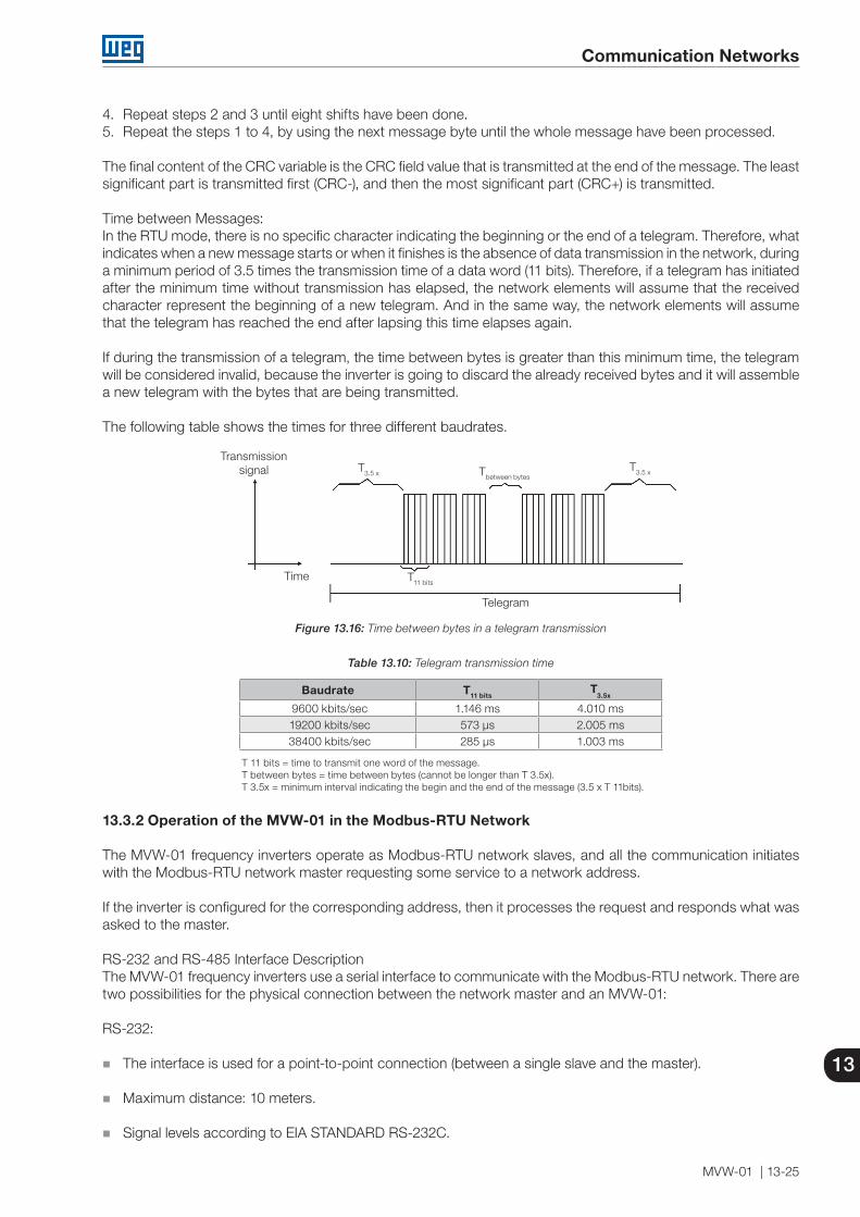
Communication Networks
MVW-01 | 13-25
13
4. Repeat steps 2 and 3 until eight shifts have been done.5. Repeat the steps 1 to 4, by using the next message byte until the whole message have been processed.
The final content of the CRC variable is the CRC field value that is transmitted at the end of the message. The leastsignificant part is transmitted first (CRC-), and then the most significant part (CRC+) is transmitted.
Time between Messages:In the RTU mode, there is no specific character indicating the beginning or the end of a telegram. Therefore, whatindicates when a new message starts or when it finishes is the absence of data transmission in the network, during a minimum period of 3.5 times the transmission time of a data word (11 bits). Therefore, if a telegram has initiated after the minimum time without transmission has elapsed, the network elements will assume that the received character represent the beginning of a new telegram. And in the same way, the network elements will assume that the telegram has reached the end after lapsing this time elapses again.
If during the transmission of a telegram, the time between bytes is greater than this minimum time, the telegram will be considered invalid, because the inverter is going to discard the already received bytes and it will assemble a new telegram with the bytes that are being transmitted.
The following table shows the times for three different baudrates.
Transmissionsignal
Time T11 bits
T3.5 x Tbetween bytesT3.5 x
Telegram
Figure 13.16: Time between bytes in a telegram transmission
Table 13.10: Telegram transmission time
Baudrate T11 bitsT
3.5x
9600 kbits/sec 1.146 ms 4.010 ms19200 kbits/sec 573 µs 2.005 ms38400 kbits/sec 285 µs 1.003 ms
T 11 bits = time to transmit one word of the message.T between bytes = time between bytes (cannot be longer than T 3.5x).T 3.5x = minimum interval indicating the begin and the end of the message (3.5 x T 11bits).
13.3.2 Operation of the MVW-01 in the Modbus-RTU Network
The MVW-01 frequency inverters operate as Modbus-RTU network slaves, and all the communication initiates with the Modbus-RTU network master requesting some service to a network address.
If the inverter is configured for the corresponding address, then it processes the request and responds what was asked to the master.
RS-232 and RS-485 Interface DescriptionThe MVW-01 frequency inverters use a serial interface to communicate with the Modbus-RTU network. There aretwo possibilities for the physical connection between the network master and an MVW-01:
RS-232:
The interface is used for a point-to-point connection (between a single slave and the master).
Maximum distance: 10 meters.
Signal levels according to EIA STANDARD RS-232C.

Communication Networks
13-26 | MVW-01
13
Three wires: transmission (TX), reception (RX) and return (0V).
RS-485:
This interface is used for multipoint connection (several slaves and the master).
Maximum distance: 1000 meters (using shielded cables).
Signal levels according to EIA STANDARD RS-485.
The EBA or the EBB expansion board, which have interface for the RS-485 communication, must be used.
Note: refer to the Item 13.2.4 RS-232 and RS-485 Physical Connection on page 13-22 which describes how to make the physical connection.
Inverter Configurations in the Modbus-RTU NetworkIn order that the inverter be able to communicate properly in the network, besides the physical connection, it is necessary to configure the inverter address, as well as the baudrate and the type of existent parity.
Inverter address in the Network:It is defined through the parameter 308.
If the type of serial communication (P312) is configured for Modbus-RTU, it is possible to select addresses from 1 to 247.
Each slave in the network must have an address different from the others.
The network master does not have an address.
It is necessary to know the address of the slave even when the connection is point-to-point.
Baudrate and Parity:
Both configurations are defined through the parameter P312.
Baudrates: 9600, 19200 or 38400 kbits/sec.
Parity: None, Odd Parity or Even Parity.
All slaves, and also the network master, must use the same baudrate and parity.
Access to the Inverter DataThrough the network, it is possible to access all the parameters and basic variables available for the MVW-01:
Parameters: they are those existing in the inverters, whose visualization and modification is possible through the Human-Machine Interface (HMI) (refer to the Parameter Quick Reference).
Basic Variables: they are internal inverter variables, and they can only be accessed via serial communication. It is possible through the basic variables, for instance, to change the speed reference, read the status, enable or disable the inverter, etc. (refer to the Item 13.2.2 Variable Code on page 13-16).
Register: name used to represent either parameters or the basic variables during the data transmission.
Internal Bits: they are bits accessed only by the serial, used for the inverter command and status monitoring.
The Item 13.2.1 Protocol Definitions on page 13-15 defines the parameter and variable resolutions when transmitted via serial.

Communication Networks
MVW-01 | 13-27
13
Available functions and response times:In the Modbus-RTU protocol specification it is defined the functions used to access the type of registers described in the specification. In the MVW-01, parameters and basic variables were defined as being holding type registers (referenced as 4x). Besides these registers, it is also possible to access directly internal command and monitoring bits (referenced as 0x). To access these bits and registers, the next services (or functions) for the MVW-01 frequency inverters were made available:Read Coils Description: reading of internal bit blocks or coils. Function code: 01. Broadcast: not supported. Response time: 5 to 10 ms.
Read Holding Registers Description: reading of register blocks of the holding type. Function code: 03. Broadcast: not supported. Response time: 5 to 10 ms.
Write Single Coil Description: writing in a single internal bit or coil. Function code: 05. Broadcast: supported. Response time: 5 to 10 ms.
Write Single Register Description: writing in a single register of the holding type. Function code: 06. Broadcast: supported. Response time: 5 to 10 ms.
Write Multiple Coils Description: writing in internal bit blocks or coils. Function code: 15. Broadcast: supported. Response time: 5 to 10 ms.
Write Multiple Registers Description: writing in register blocks of holding type. Function code: 16. Broadcast: supported. Response time: 10 to 20 ms for each written register.
Read Device Identification Description: Identification of the inverter model. Function code: 43. Broadcast: not supported. Response time: 5 to 10 ms.
Note: Modbus-RTU network slaves are addressed from 1 to 247. The master uses the address 0 to send messagesthat are destined to all slaves (broadcast).
Data Addressing and Offset:The data addressing in the MVW-01 is done with offset equal to zero, meaning that the number of the address isequal to the given number. The parameters are made available starting from the address 0 (zero), while the basicvariables are made available starting from the address 5000. In the same way, the status bits are made availablestarting from the address 0 (zero) and the command bytes are made available beginning from the address 100.
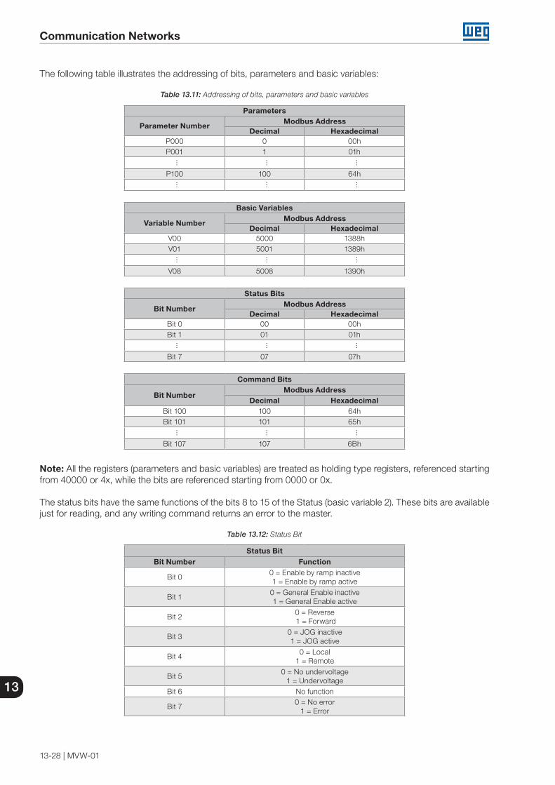
Communication Networks
13-28 | MVW-01
13
The following table illustrates the addressing of bits, parameters and basic variables:
Table 13.11: Addressing of bits, parameters and basic variables
Parameters
Parameter NumberModbus Address
Decimal HexadecimalP000 0 00hP001 1 01h
... ... ...
P100 100 64h... ... ...
Basic Variables
Variable NumberModbus Address
Decimal HexadecimalV00 5000 1388hV01 5001 1389h
... ... ...
V08 5008 1390h
Status Bits
Bit NumberModbus Address
Decimal HexadecimalBit 0 00 00hBit 1 01 01h
... ... ...Bit 7 07 07h
Command Bits
Bit NumberModbus Address
Decimal HexadecimalBit 100 100 64hBit 101 101 65h
... ... ...
Bit 107 107 6Bh
Note: All the registers (parameters and basic variables) are treated as holding type registers, referenced starting from 40000 or 4x, while the bits are referenced starting from 0000 or 0x.
The status bits have the same functions of the bits 8 to 15 of the Status (basic variable 2). These bits are availablejust for reading, and any writing command returns an error to the master.
Table 13.12: Status Bit
Status BitBit Number Function
Bit 00 = Enable by ramp inactive 1 = Enable by ramp active
Bit 10 = General Enable inactive1 = General Enable active
Bit 20 = Reverse 1 = Forward
Bit 30 = JOG inactive1 = JOG active
Bit 40 = Local
1 = Remote
Bit 50 = No undervoltage
1 = UndervoltageBit 6 No function
Bit 70 = No error
1 = Error
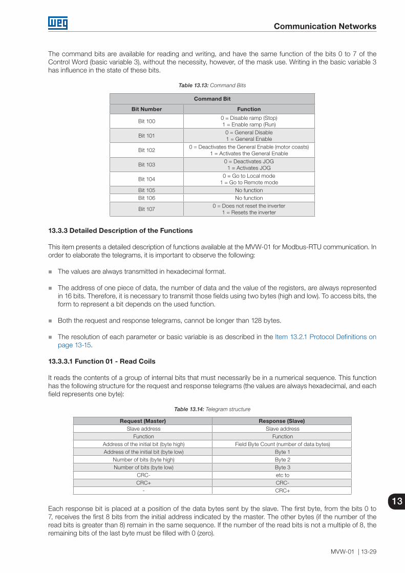
Communication Networks
MVW-01 | 13-29
13
The command bits are available for reading and writing, and have the same function of the bits 0 to 7 of the Control Word (basic variable 3), without the necessity, however, of the mask use. Writing in the basic variable 3 has influence in the state of these bits.
Table 13.13: Command Bits
Command Bit
Bit Number Function
Bit 1000 = Disable ramp (Stop) 1 = Enable ramp (Run)
Bit 1010 = General Disable 1 = General Enable
Bit 1020 = Deactivates the General Enable (motor coasts)
1 = Activates the General Enable
Bit 1030 = Deactivates JOG
1 = Activates JOG
Bit 1040 = Go to Local mode
1 = Go to Remote modeBit 105 No functionBit 106 No function
Bit 1070 = Does not reset the inverter
1 = Resets the inverter
13.3.3 Detailed Description of the Functions
This item presents a detailed description of functions available at the MVW-01 for Modbus-RTU communication. Inorder to elaborate the telegrams, it is important to observe the following:
The values are always transmitted in hexadecimal format.
The address of one piece of data, the number of data and the value of the registers, are always represented in 16 bits. Therefore, it is necessary to transmit those fields using two bytes (high and low). To access bits, the form to represent a bit depends on the used function.
Both the request and response telegrams, cannot be longer than 128 bytes.
The resolution of each parameter or basic variable is as described in the Item 13.2.1 Protocol Definitions on page 13-15.
13.3.3.1 Function 01 - Read Coils
It reads the contents of a group of internal bits that must necessarily be in a numerical sequence. This function has the following structure for the request and response telegrams (the values are always hexadecimal, and each field represents one byte):
Table 13.14: Telegram structure
Request (Master) Response (Slave)Slave address Slave address
Function FunctionAddress of the initial bit (byte high) Field Byte Count (number of data bytes)Address of the initial bit (byte low) Byte 1
Number of bits (byte high) Byte 2Number of bits (byte low) Byte 3
CRC- etc toCRC+ CRC-
- CRC+
Each response bit is placed at a position of the data bytes sent by the slave. The first byte, from the bits 0 to 7, receives the first 8 bits from the initial address indicated by the master. The other bytes (if the number of the read bits is greater than 8) remain in the same sequence. If the number of the read bits is not a multiple of 8, the remaining bits of the last byte must be filled with 0 (zero).

Communication Networks
13-30 | MVW-01
13
Example: reading the status bits for general enable (bit 1) and Forward/Reverse (bit 2) of then MVW-01 at the address 1:
Table 13.15: Example of telegram structure
Request (Master) Response (Slave)
Field Value Field ValueSlave address 01h Slave address 01h
Function 01h Function 01hInitial byte address (byte high) 00h Byte Count 01hInitial byte address (byte low) 01h Status of bits 1 and 2 02h
Number of bits (byte high) 00h CRC- D0hNumber of bits (byte low) 02h CRC+ 49h
CRC- ECh - -CRC+ 0Bh - -
As the number of read bits in the example is smaller than 8, the slave required only 1 byte for the response. The value of the byte was 02h, which as binary value will have the form 0000 0010. As the number of read bits is equal to 2, only the two less significant bits, that have the value 0 (General Enable inactive) and 1 (Forward) are of interest. The other bits, as they had not been requested, are filled out with 0 (zero).
13.3.3.2 Function 03 - Read Holding Register
It reads the contents of a group registers that must necessarily be in a numerical sequence. This function has thefollowing structure for the request and response telegrams (the values are always hexadecimal, and each field represents one byte):
Table 13.16: Telegram structure
Request (Master) Response (Slave)Slave address Slave address
Function FunctionAddress of the initial register (byte high) Campo Byte CountAddress of the initial register (byte low) Data 1 (high)
Number of registers (byte high) Data 1 (low)Number of registers (byte low) Data 2 (high)
CRC- Data 2 (low)CRC+ etc
- CRC-- CRC+
Example: Reading of the motor speed (P002) and motor current (P003) from the MVW-01 at the address 1:
Table 13.17: Example of telegram structure
Request (Master) Response (Slave)
Field Value Field ValueSlave address 01h Slave address 01h
Function 03h Function 03hInitial register (byte high) 00h Byte Count 04hInitial register (byte low) 02h P002 (high) 05h
Number of registers (byte high) 00h P002 (low) 84hNumber of registers (byte low) 02h P003 (high) 00h
CRC- 65h P003 (low) 35hCRC+ CBh CRC- 7Ah
- - CRC+ 49h
Each register is always formed by two bytes (high and low). For the example, we have P002 = 0384h, that in decimal number is equal to 900. As this parameter does not have a decimal place, the actual read value is 900 rpm.

Communication Networks
MVW-01 | 13-31
13
In the same way we will have a motor current value at P003 = 0035h, which corresponds to 53 decimal. As the current has one decimal digit resolution, the read value is 5.3 A.
13.3.3.3 Function 05 - Write Single Coil
This function is used to write a value to a single bit. The bit value is represented by using two bytes, where FF00hrepresents the bit that is equal to 1, and 0000h represents the bit that is equal to 0 (zero). It has the following structure (the values are always hexadecimal, and each field represents one byte):
Table 13.18: Telegram structure
Request (Master) Response (Slave)Slave address Slave address
Function FunctionBit address (byte high) Bit address (byte high)Bit address (byte low) Bit address (byte low)Bit value (byte high) Bit value (byte high)Bit value (byte low) Bit value (byte low)
CRC- CRC-CRC+ CRC+
Example: to activate the start command (bit 100 = 1) of an MVW-01 at the address 1:
Table 13.19: Example of telegram structure
Request (Master) Response (Slave)
Field Value Field ValueSlave address 01h Slave address 01h
Function 05h Function 01hBit number (byte high) 00h Bit number (byte high) 01hBit number (byte low) 64h Bit number (byte low) 02hBit value (byte high) FFh Bit value (byte high) D0hBit value (byte low) 00h Bit value (byte low) 49h
CRC- CDh CRC- CDhCRC+ E5h CRC+ E5h
For this function, the slave response is an identical copy of the request sent by the master.
13.3.3.4 Function 06 - Write Single Register
This function is used to write a value to a single register. This function has the following structure (values are alwayshexadecimal values, and each field represents one byte):
Table 13.20: Telegram structure
Request (Master) Response (Slave)Slave address Slave address
Function FunctionRegister address (byte high) Register address (byte high)Register address (byte low) Register address (byte low)
Value for the register (byte high) Value for the register (byte high)Value for the register (byte low) Value for the register (byte low)
CRC- CRC-CRC+ CRC+
Example: Writing a speed reference (basic variable 4) equal to 900 rpm, to an MVW-01 at the address1.
It is useful to remember that the value for the basic variable 4 depends on the used motor type and that the value 8191 is equal to the rated motor speed. In this case, we suppose that the used motor has a rated speed of 1800 rpm, thus the value to be written into the basic variable 4 for a speed of 900 rpm is half of 8191, i.e., 4096 (1000h).
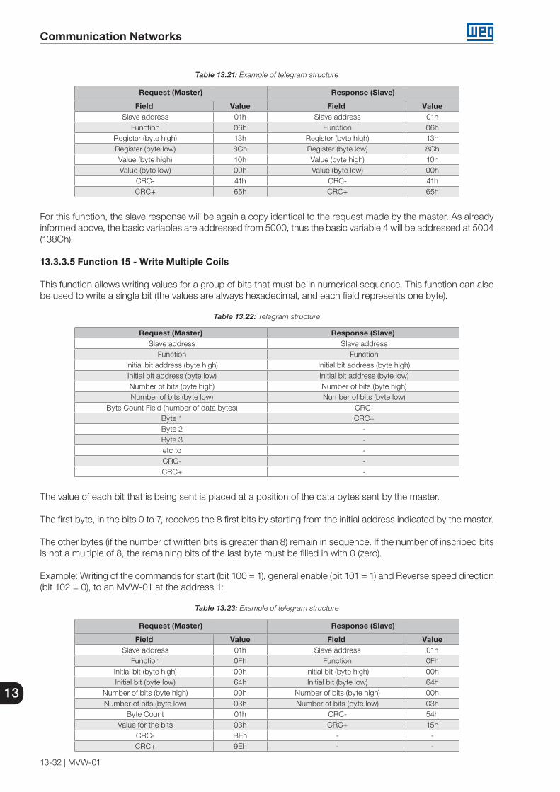
Communication Networks
13-32 | MVW-01
13
Table 13.21: Example of telegram structure
Request (Master) Response (Slave)
Field Value Field ValueSlave address 01h Slave address 01h
Function 06h Function 06hRegister (byte high) 13h Register (byte high) 13hRegister (byte low) 8Ch Register (byte low) 8ChValue (byte high) 10h Value (byte high) 10hValue (byte low) 00h Value (byte low) 00h
CRC- 41h CRC- 41hCRC+ 65h CRC+ 65h
For this function, the slave response will be again a copy identical to the request made by the master. As alreadyinformed above, the basic variables are addressed from 5000, thus the basic variable 4 will be addressed at 5004(138Ch).
13.3.3.5 Function 15 - Write Multiple Coils
This function allows writing values for a group of bits that must be in numerical sequence. This function can alsobe used to write a single bit (the values are always hexadecimal, and each field represents one byte).
Table 13.22: Telegram structure
Request (Master) Response (Slave)Slave address Slave address
Function FunctionInitial bit address (byte high) Initial bit address (byte high)Initial bit address (byte low) Initial bit address (byte low)Number of bits (byte high) Number of bits (byte high)Number of bits (byte low) Number of bits (byte low)
Byte Count Field (number of data bytes) CRC-Byte 1 CRC+Byte 2 -Byte 3 -etc to -CRC- -CRC+ -
The value of each bit that is being sent is placed at a position of the data bytes sent by the master.
The first byte, in the bits 0 to 7, receives the 8 first bits by starting from the initial address indicated by the master.
The other bytes (if the number of written bits is greater than 8) remain in sequence. If the number of inscribed bitsis not a multiple of 8, the remaining bits of the last byte must be filled in with 0 (zero).
Example: Writing of the commands for start (bit 100 = 1), general enable (bit 101 = 1) and Reverse speed direction(bit 102 = 0), to an MVW-01 at the address 1:
Table 13.23: Example of telegram structure
Request (Master) Response (Slave)
Field Value Field ValueSlave address 01h Slave address 01h
Function 0Fh Function 0FhInitial bit (byte high) 00h Initial bit (byte high) 00hInitial bit (byte low) 64h Initial bit (byte low) 64h
Number of bits (byte high) 00h Number of bits (byte high) 00hNumber of bits (byte low) 03h Number of bits (byte low) 03h
Byte Count 01h CRC- 54hValue for the bits 03h CRC+ 15h
CRC- BEh - -CRC+ 9Eh - -
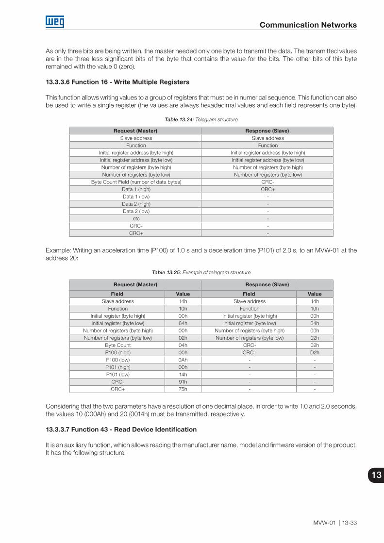
Communication Networks
MVW-01 | 13-33
13
As only three bits are being written, the master needed only one byte to transmit the data. The transmitted values are in the three less significant bits of the byte that contains the value for the bits. The other bits of this byte remained with the value 0 (zero).
13.3.3.6 Function 16 - Write Multiple Registers
This function allows writing values to a group of registers that must be in numerical sequence. This function can alsobe used to write a single register (the values are always hexadecimal values and each field represents one byte).
Table 13.24: Telegram structure
Request (Master) Response (Slave)Slave address Slave address
Function FunctionInitial register address (byte high) Initial register address (byte high)Initial register address (byte low) Initial register address (byte low)Number of registers (byte high) Number of registers (byte high)Number of registers (byte low) Number of registers (byte low)
Byte Count Field (number of data bytes) CRC-Data 1 (high) CRC+Data 1 (low) -Data 2 (high) -Data 2 (low) -
etc -CRC- -CRC+ -
Example: Writing an acceleration time (P100) of 1.0 s and a deceleration time (P101) of 2.0 s, to an MVW-01 at the address 20:
Table 13.25: Example of telegram structure
Request (Master) Response (Slave)
Field Value Field ValueSlave address 14h Slave address 14h
Function 10h Function 10hInitial register (byte high) 00h Initial register (byte high) 00hInitial register (byte low) 64h Initial register (byte low) 64h
Number of registers (byte high) 00h Number of registers (byte high) 00hNumber of registers (byte low) 02h Number of registers (byte low) 02h
Byte Count 04h CRC- 02hP100 (high) 00h CRC+ D2hP100 (low) 0Ah - -P101 (high) 00h - -P101 (low) 14h - -
CRC- 91h - -CRC+ 75h - -
Considering that the two parameters have a resolution of one decimal place, in order to write 1.0 and 2.0 seconds,the values 10 (000Ah) and 20 (0014h) must be transmitted, respectively.
13.3.3.7 Function 43 - Read Device Identification
It is an auxiliary function, which allows reading the manufacturer name, model and firmware version of the product.It has the following structure:
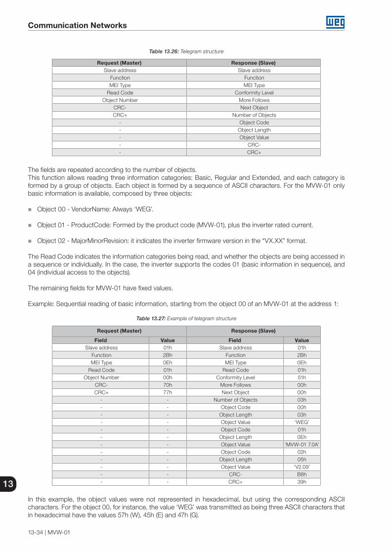
Communication Networks
13-34 | MVW-01
13
Table 13.26: Telegram structure
Request (Master) Response (Slave)Slave address Slave address
Function FunctionMEI Type MEI Type
Read Code Conformity LevelObject Number More Follows
CRC- Next ObjectCRC+ Number of Objects
- Object Code- Object Length- Object Value- CRC-- CRC+
The fields are repeated according to the number of objects.This function allows reading three information categories: Basic, Regular and Extended, and each category is formed by a group of objects. Each object is formed by a sequence of ASCII characters. For the MVW-01 only basic information is available, composed by three objects:
Object 00 - VendorName: Always ‘WEG’.
Object 01 - ProductCode: Formed by the product code (MVW-01), plus the inverter rated current.
Object 02 - MajorMinorRevision: it indicates the inverter firmware version in the “VX.XX” format.
The Read Code indicates the information categories being read, and whether the objects are being accessed ina sequence or individually. In the case, the inverter supports the codes 01 (basic information in sequence), and 04 (individual access to the objects).
The remaining fields for MVW-01 have fixed values.
Example: Sequential reading of basic information, starting from the object 00 of an MVW-01 at the address 1:
Table 13.27: Example of telegram structure
Request (Master) Response (Slave)
Field Value Field ValueSlave address 01h Slave address 01h
Function 2Bh Function 2BhMEI Type 0Eh MEI Type 0Eh
Read Code 01h Read Code 01hObject Number 00h Conformity Level 51h
CRC- 70h More Follows 00hCRC+ 77h Next Object 00h
- - Number of Objects 03h- - Object Code 00h- - Object Length 03h- - Object Value ‘WEG’- - Object Code 01h- - Object Length 0Eh- - Object Value ‘MVW-01 7.0A’- - Object Code 02h- - Object Length 05h- - Object Value ‘V2.09’- - CRC- B8h- - CRC+ 39h
In this example, the object values were not represented in hexadecimal, but using the corresponding ASCII characters. For the object 00, for instance, the value ‘WEG’ was transmitted as being three ASCII characters thatin hexadecimal have the values 57h (W), 45h (E) and 47h (G).

Communication Networks
MVW-01 | 13-35
13
13.3.4 ModBus RTU Communication Error
Errors may occur in telegram transmission through the network, or in the contents of the received telegrams.According to the type of error, the inverter may or may not send a response to the master:When the master sends a message to an inverter configured at a specific network address, the inverter will not respond to the master if the following occurs:
Parity bit error.
CRC error.
Timeout between transmitted bytes (3.5 times the transmission time of a 11 bit word).
In the case of a successful reception, during the telegram processing the inverter may detect problems, and sendan error message, indicating the type of problem found:
Invalid function (error code = 1): the requested function has not been implemented for the inverter.
Invalid data address (error code = 2): the data address (register or bit) does not exist.
Data value invalid (error code = 3): this error occurs in the following conditions:
Value is out of the permitted range.
Writing in data that cannot be changed (read-only register, or one that does not allow changing with enabled inverter, or Status Word bits).
Writing in a Control Word function that has not been enabled via serial interface.
Error MessagesWhen any error occurs in the message content (not during the data transfer), the slave must return a message indicating the error type that occurred. The errors that may occur in the MVW-01 during the message processing are invalid function (code 01), invalid data address (code 02), and invalid data value (code 03) errors.
The messages sent by the slave have following structure:
Table 13.28: Telegram structure
Response (Slave)Slave addressFunction code
(with most significant bit to 1)Error code
CRC-CRC+
Example: The master requests the slave at address 1 to write in the parameter 89 (inexistent parameter):
Table 13.29: Example of telegram structure
Request (Master) Response (Slave)
Field Value Field ValueSlave address 01h Slave address 01h
Function 06h Function 86hRegister (high) 00h Error code 02hRegister (low) 59h CRC- C3hValue (high) 00h CRC+ A1hValue (low) 00h - -
CRC- 59h - -CRC+ D9h - -

Communication Networks
13-36 | MVW-01
13
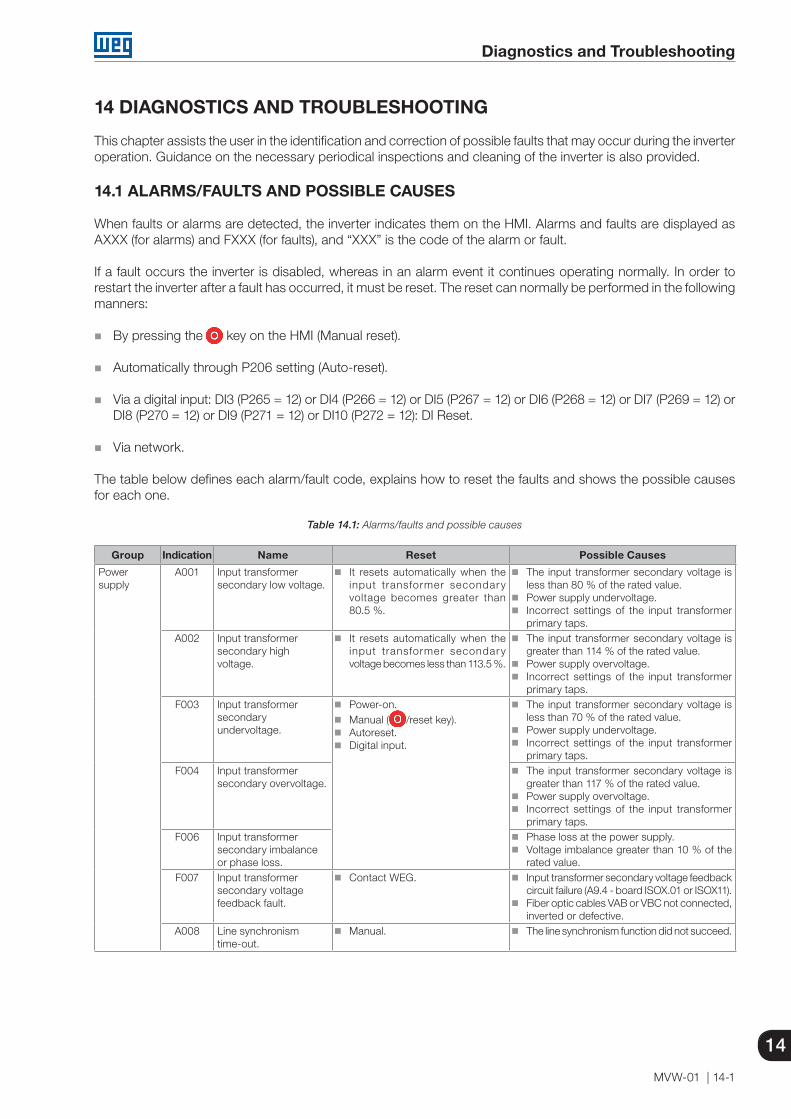
Diagnostics and Troubleshooting
MVW-01 | 14-1
14
14 DIAGNOSTICS AND TROUBLESHOOTING
This chapter assists the user in the identification and correction of possible faults that may occur during the inverter operation. Guidance on the necessary periodical inspections and cleaning of the inverter is also provided.
14.1 ALARMS/FAULTS AND POSSIBLE CAUSES
When faults or alarms are detected, the inverter indicates them on the HMI. Alarms and faults are displayed as AXXX (for alarms) and FXXX (for faults), and “XXX” is the code of the alarm or fault.
If a fault occurs the inverter is disabled, whereas in an alarm event it continues operating normally. In order to restart the inverter after a fault has occurred, it must be reset. The reset can normally be performed in the followingmanners:
By pressing the key on the HMI (Manual reset).
Automatically through P206 setting (Auto-reset).
Via a digital input: DI3 (P265 = 12) or DI4 (P266 = 12) or DI5 (P267 = 12) or DI6 (P268 = 12) or DI7 (P269 = 12) or DI8 (P270 = 12) or DI9 (P271 = 12) or DI10 (P272 = 12): DI Reset.
Via network.
The table below defines each alarm/fault code, explains how to reset the faults and shows the possible causes for each one.
Table 14.1: Alarms/faults and possible causes
Group Indication Name Reset Possible Causes
Power supply
A001 Input transformer secondary low voltage.
It resets automatically when the input transformer secondary voltage becomes greater than 80.5 %.
The input transformer secondary voltage is less than 80 % of the rated value.
Power supply undervoltage. Incorrect settings of the input transformer
primary taps.A002 Input transformer
secondary high voltage.
It resets automatically when the input transformer secondary voltage becomes less than 113.5 %.
The input transformer secondary voltage is greater than 114 % of the rated value.
Power supply overvoltage. Incorrect settings of the input transformer
primary taps.F003 Input transformer
secondary undervoltage.
Power-on. Manual ( /reset key). Autoreset. Digital input.
The input transformer secondary voltage is less than 70 % of the rated value.
Power supply undervoltage. Incorrect settings of the input transformer
primary taps.F004 Input transformer
secondary overvoltage. The input transformer secondary voltage is
greater than 117 % of the rated value. Power supply overvoltage. Incorrect settings of the input transformer
primary taps.F006 Input transformer
secondary imbalance or phase loss.
Phase loss at the power supply. Voltage imbalance greater than 10 % of the
rated value.F007 Input transformer
secondary voltage feedback fault.
Contact WEG. Input transformer secondary voltage feedback circuit failure (A9.4 - board ISOX.01 or ISOX11).
Fiber optic cables VAB or VBC not connected, inverted or defective.
A008 Line synchronism time-out.
Manual. The line synchronism function did not succeed.
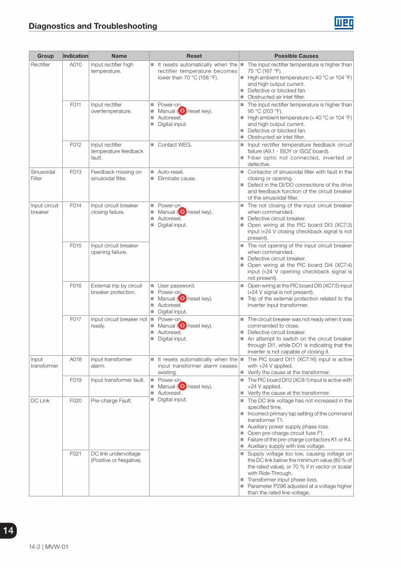
Diagnostics and Troubleshooting
14-2 | MVW-01
14
Group Indication Name Reset Possible Causes
Rectifier A010 Input rectifier high temperature.
It resets automatically when the rectifier temperature becomes lower than 70 °C (158 °F).
The input rectifier temperature is higher than 75 °C (167 °F).
High ambient temperature (> 40 °C or 104 °F) and high output current.
Defective or blocked fan. Obstructed air inlet filter.
F011 Input rectifier overtemperature.
Power-on. Manual ( /reset key). Autoreset. Digital input.
The input rectifier temperature is higher than 95 °C (203 °F).
High ambient temperature (> 40 °C or 104 °F) and high output current.
Defective or blocked fan. Obstructed air inlet filter.
F012 Input rectifier temperature feedback fault.
Contact WEG. Input rectifier temperature feedback circuit failure (A9.1 - ISOY or ISOZ board).
Fiber optic not connected, inverted or defective.
Sinusoidal Filter
F013 Feedback missing on sinusoidal filter.
Auto-reset. Eliminate cause.
Contactor of sinusoidal filter with fault in the closing or opening.
Defect in the DI/DO connections of the drive and feedback function of the circuit breaker of the sinusoidal filter.
Input circuit breaker
F014 Input circuit breaker closing failure.
Power-on. Manual ( /reset key). Autoreset. Digital input.
The not closing of the input circuit breaker when commanded.
Defective circuit breaker. Open wiring at the PIC board DI3 (XC7:3)
input (+24 V closing checkback signal is not present).
F015 Input circuit breaker opening failure.
The not opening of the input circuit breaker when commanded.
Defective circuit breaker. Open wiring at the PIC board DI4 (XC7:4)
input (+24 V opening checkback signal is not present).
F016 External trip by circuit breaker protection.
User password. Power-on. Manual ( /reset key). Autoreset. Digital input.
Open wiring at the PIC board DI5 (XC7:5) input (+24 V signal is not present).
Trip of the external protection related to the inverter input transformer.
F017 Input circuit breaker not ready.
Power-on. Manual ( /reset key). Autoreset. Digital input.
The circuit breaker was not ready when it was commanded to close.
Defective circuit breaker. An attempt to switch on the circuit breaker
through DI1, while DO1 is indicating that the inverter is not capable of closing it.
Input transformer
A018 Input transformer alarm.
It resets automatically when the input transformer alarm ceases existing.
The PIC board DI11 (XC7:16) input is active with +24 V applied.
Verify the cause at the transformer.F019 Input transformer fault. Power-on.
Manual ( /reset key). Autoreset. Digital input.
The PIC board DI12 (XC8:1) input is active with +24 V applied.
Verify the cause at the transformer.DC Link F020 Pre-charge Fault. The DC link voltage has not increased in the
specified time. Incorrect primary tap setting of the command
transformer T1. Auxiliary power supply phase loss. Open pre-charge circuit fuse F1. Failure of the pre-charge contactors K1 or K4. Auxiliary supply with low voltage.
F021 DC link undervoltage (Positive or Negative).
Supply voltage too low, causing voltage on the DC link below the minimum value (80 % of the rated value), or 70 % if in vector or scalar with Ride-Through.
Transformer input phase loss. Parameter P296 adjusted at a voltage higher
than the rated line voltage.

Diagnostics and Troubleshooting
MVW-01 | 14-3
14
Group Indication Name Reset Possible Causes
DC Link F022 DC link overvoltage(Positive or Negative).
Power-on. Manual ( /reset key). Autoreset. Digital input.
The power supply voltage is too high producing a DC link voltage higher than the maximum 130 % of the nominal value).
The load inertia is too high or the deceleration ramp is too fast.
P151 or P153 setting is too high.F023 DC link imbalance. The difference between the positive and
the negative DC link voltages > 15 % of the rated value.
F024 Positive or negative DClink voltage feedback fault.
Contact WEG. DC link voltage feedback circuit failure (Positive or Negative): A9.3 - board ISOX.00 or ISOX.10.
Fiber optic cables VP or VN not connected, inverted or defective.
F025 Door closing fault. Power-on. Manual ( /reset key). Autoreset. Digital input.
An attempt to power-up the inverter with open cabinet doors.
Open wiring at the PIC board DI16 (XC8:10) input (+24 V indicating closed doors is not present).
F026 Input circuit breaker not ready.
An attempt to power-up the inverter while the input circuit breaker was not ready.
Defective circuit breaker. The circuit breaker is indicating, through DI2,
that the attempt to close it has failed.Inverter F030 U 1 IGBT fault. Contact WEG. Related to the gate driver fault feedback.
IGBT out of the saturation zone. Fiber optic poorly connected or defective.
F031 U 2 IGBT fault.F032 U 3 IGBT fault.F033 U 4 IGBT fault.F034 V 1 IGBT fault.F035 V 2 IGBT fault.F036 V 3 IGBT fault.F037 V 4 IGBT fault.F038 W 1 IGBT fault.F039 W 2 IGBT fault.F040 W 3 IGBT fault.F041 W 4 IGBT fault.F042 Braking IGBT 1 fault. Related to the gate driver fault feedback, its
power supply or the IGBT desaturation. Fiber optic cable not connected, inverted or
defective.
F043 Braking IGBT 2 fault.
F044 Arc detection. Electrical arcing detection by cabinet sensors.F045 PS1/PS1S power supply
fault. Problem with the PS1 power supply, located
in the rectifier column. Fiber optic cable not connected, inverted or
defective.A046 Motor I x t overload
alarm. It resets automatically when the
over load status value (P076) becomes lower than P159.
The P159 setting is too low for the used motor. Too heavy load at the motor shaft. P136 and P137 settings are too high (valid for
low speed operation).F047 IGBT overload fault. Manual. A high current transitory occurred while the
heatsink was with high temperature. Actuation of the fault at 120 °C (248 °F).
F048 Forced ventilation fault. Obstructed fans. Obstructed air inlet filters.
A050 U phase heatsink hightemperature.
It resets automatically when the U phase heatsink temperature becomes lower than 70 °C (158 °F).
U phase heatsink temperature is higher than 75 °C (167 °F).
High ambient temperature (> 40 °C or 104 °F) and high output curren.
Defective or blocked fans. Obstructed air inlet filters.
F051 U phase heatsinkovertemperature.
Power-on. Manual ( /reset key). Autoreset. Digital input.
U phase heatsink temperature is higher than 80 °C (176 °F).
High ambient temperature (> 40 °C or 104 °F) and high output current.
Defective or blocked fans. Obstructed air inlet filters.

Diagnostics and Troubleshooting
14-4 | MVW-01
14
Group Indication Name Reset Possible Causes
Inverter F052 U phase heatsinktemperature feedbackfault.
Contact WEG. U phase heatsink temperature feedback circuit failure.
Fiber optic cable TEMPU not connected, inverted or defective.
A053 V phase heatsink hightemperature.
It resets automatically when the V phase heatsink temperature becomes lower than 70 °C (158 °F).
V phase heatsink temperature is higher than 75 °C (167 °F).
High ambient temperature (> 40 °C or 104 °F) and high output current.
Defective or blocked fans. Obstructed air inlet filters.
F054 V phase heatsinkovertemperature.
Power-on. Manual ( /reset key). Autoreset. Digital input.
V phase heatsink temperature is higher than 80 °C (176 °F).
High ambient temperature (> 40 °C or 104 °F) and high output current.
Defective or blocked fans. Obstructed air inlet filters.
F055 V phase heatsinktemperature feedbackfault.
Contact WEG. V phase heatsink temperature feedback circuit failure.
Fiber optic cable TEMPV not connected, inverted or defective.
A056 W phase heatsink hightemperature.
It resets automatically when the W phase heatsink temperature becomes lower than 70 °C (158 °F).
W phase heatsink temperature is higher than 75 °C (167 °F).
High ambient temperature (> 40 °C or 104 °F) and high output current.
Defective or blocked fans. Obstructed air inlet filters.
F057 W phase heatsinkovertemperature.
Power-on. Manual ( /reset key). Autoreset. Digital input.
W phase heatsink temperature is higher than 80 °C (176 °F).
High ambient temperature (> 40 °C or 104 °F) and high output current.
Defective or blocked fans. Obstructed air inlet filters.
F058 W phase heatsinktemperature feedbackfault.
Contact WEG. W phase heatsink temperature feedback circuit failure.
Fiber optic cable TEMPW not connected, inverted or defective.
A059 Braking arm hightemperature.
It resets automatically when the braking arm temperature becomes lower than 70 °C (158 °F).
Braking arm temperature is higher than 75 °C (167 °F).
High ambient temperature (> 40 °C or 104 °F) and high output current.
Defective or blocked fans. Obstructed air inlet filters.
F060 Braking armovertemperature.
Power-on. Manual ( /reset key). Autoreset. Digital input.
Braking arm temperature is higher than 80 °C (176 °F).
High ambient temperature (> 40 °C or 104 °F) and high output current.
Defective or blocked fans. Obstructed air inlet filters.
F061 Braking arm temperature feedback fault.
Contact WEG. Braking arm temperature feedback circuit failure.
Fiber optic cable TEMPBR not connected, inverted or defective.
F062 Thermal imbalanceamong the U, V and Wphase heatsinks.
Power-on. Manual ( /reset key). Autoreset. Digital input.
Temperature difference among the U, V and W phase heatsinks greater than 10 °C (50 °F).
High ambient temperature (> 40 °C or 104 °F) and high output current
Defective or blocked fans. Obstructed air inlet filters.
Powersection test
F063 U output voltage feedback fault.
For WEG use. For WEG use.
F064 V output voltage feedback fault.
F065 W output voltage feedback fault.
Self-tuning/Test mode
F066 Null current.F068 Test mode.F069 Calibration fault.

Diagnostics and Troubleshooting
MVW-01 | 14-5
14
Group Indication Name Reset Possible Causes
Output/Motor
F070 Overcurrent/Shortcircuitat the output.
Power-on. Manual ( /reset key). Autoreset. Digital input.
Instant current in the motor output ≥1.8 times the rated current of the inverter (Detection by Hardware).
Short-circuit between two motor phases or power cables.
Short-circuit between motor cables and the ground.
Load inertia is too high or acceleration ramp is too fast.
Shorted IGBT modules. Incorrect regulation and/or configuration
parameters. P169 setting is too high.
F071 Overcurrent at theoutput.
High current at the three phases (software detection).
Load inertia is too high or acceleration ramp is too fast.
Incorrect regulation and/or configuration parameters.
P169 setting is too high.F072 Motor I x t overload. P156, P157 and P158 settings are too low for
the used motor. P136 and P137 settings are too high (valid for
low speed operation). Too heavy load at the motor shaft. The output overload fault does not cause the
input circuit breaker opening.A073 Ground fault alarm. It resets automatically when the
cause ceases existing. Shor t-c i rcu i t to the ground in some
point detected by software through the measurement of the feedback signal by fiber optic of the voltage Medium Point (PM) to the ground > 25 %, the sum of the output currents is greater than 10 % of the rated current or current measurement CT defective.
F074 Ground fault. Manual. Auto-reset.
Time limit, for operation with ground fault has elapsed.
The sum of the output currents is greater than 10 % of the rated current.
Current measurement CT defective.F075 Failure feedback of
voltage between the Medium Point (MP) DC Link and ground.
Contact WEG. Failure feedback circuit of voltage between the Ponto-Medio (PM) DC Link and ground (GND).
Fiber optic cable not connected, inverted or defective.
F076 Motor phase loss. Power-on. Manual ( /reset key). Autoreset. Digital input.
Bad contact at the motor cables. Current feedback circuit failure.
F077 Braking resistoroverload.
The load inertia is too high or the deceleration ramp is too fast.
Too heavy load at the motor shaft. P154 and/or P155 programmed incorrectly.
F078 Motor overtemperature. Deactivation of the digital input programmed for “Motor fault”.
Actuation of the external thermal relay (Tecsystem or Pextron).
F079 Encoder fault. Power-on. Manual/automatic. Autoreset.
Interrupted wiring between the encoder and the encoder interface accessory.
Defective encoder. Cable length longer than the maximum limit
specified. Mounting error of the absolute encoder.
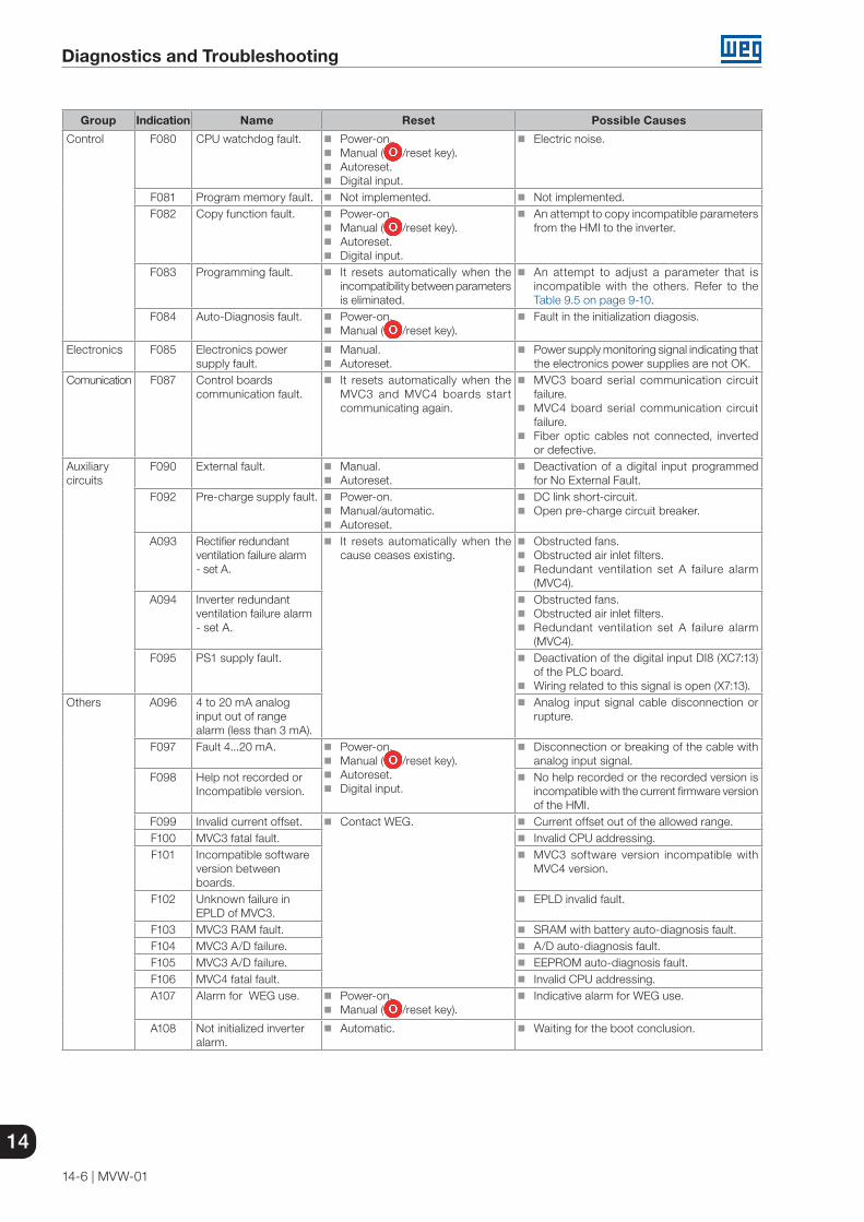
Diagnostics and Troubleshooting
14-6 | MVW-01
14
Group Indication Name Reset Possible Causes
Control F080 CPU watchdog fault. Power-on. Manual ( /reset key). Autoreset. Digital input.
Electric noise.
F081 Program memory fault. Not implemented. Not implemented.F082 Copy function fault. Power-on.
Manual ( /reset key). Autoreset. Digital input.
An attempt to copy incompatible parameters from the HMI to the inverter.
F083 Programming fault. It resets automatically when the incompatibility between parameters is eliminated.
An attempt to adjust a parameter that is incompatible with the others. Refer to the Table 9.5 on page 9-10.
F084 Auto-Diagnosis fault. Power-on. Manual ( /reset key).
Fault in the initialization diagosis.
Electronics F085 Electronics power supply fault.
Manual. Autoreset.
Power supply monitoring signal indicating that the electronics power supplies are not OK.
Comunication F087 Control boards communication fault.
It resets automatically when the MVC3 and MVC4 boards start communicating again.
MVC3 board serial communication circuit failure.
MVC4 board serial communication circuit failure.
Fiber optic cables not connected, inverted or defective.
Auxiliarycircuits
F090 External fault. Manual. Autoreset.
Deactivation of a digital input programmed for No External Fault.
F092 Pre-charge supply fault. Power-on. Manual/automatic. Autoreset.
DC link short-circuit. Open pre-charge circuit breaker.
A093 Rectifier redundant ventilation failure alarm - set A.
It resets automatically when the cause ceases existing.
Obstructed fans. Obstructed air inlet filters. Redundant ventilation set A failure alarm
(MVC4).A094 Inverter redundant
ventilation failure alarm - set A.
Obstructed fans. Obstructed air inlet filters. Redundant ventilation set A failure alarm
(MVC4).F095 PS1 supply fault. Deactivation of the digital input DI8 (XC7:13)
of the PLC board. Wiring related to this signal is open (X7:13).
Others A096 4 to 20 mA analoginput out of rangealarm (less than 3 mA).
Analog input signal cable disconnection or rupture.
F097 Fault 4...20 mA. Power-on. Manual ( /reset key). Autoreset. Digital input.
Disconnection or breaking of the cable with analog input signal.
F098 Help not recorded or Incompatible version.
No help recorded or the recorded version is incompatible with the current firmware version of the HMI.
F099 Invalid current offset. Contact WEG. Current offset out of the allowed range.F100 MVC3 fatal fault. Invalid CPU addressing.F101 Incompatible software
version betweenboards.
MVC3 software version incompatible with MVC4 version.
F102 Unknown failure in EPLD of MVC3.
EPLD invalid fault.
F103 MVC3 RAM fault. SRAM with battery auto-diagnosis fault.F104 MVC3 A/D failure. A/D auto-diagnosis fault.F105 MVC3 A/D failure. EEPROM auto-diagnosis fault.F106 MVC4 fatal fault. Invalid CPU addressing.A107 Alarm for WEG use. Power-on.
Manual ( /reset key). Indicative alarm for WEG use.
A108 Not initialized inverteralarm.
Automatic. Waiting for the boot conclusion.
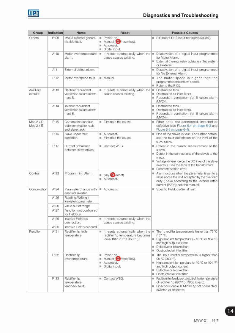
Diagnostics and Troubleshooting
MVW-01 | 14-7
14
Group Indication Name Reset Possible Causes
Others F109 MVC3 external general disable fault.
Power-on. Manual ( /reset key). Autoreset. Digital input.
PIC board DI13 input not active (XC8:7).
A110 Motor overtemperature alarm.
It resets automatically when the cause ceases existing.
Deactivation of a digital input programmed for Motor Alarm.
External thermal relay actuation (Tecsystem or Pextron).
A111 External defect alarm. Deactivation of a digital input programmed for No External Alarm.
F112 Motor overspeed fault. Manual. The motor speed is h igher than the programmed maximum speed.
Refer to the P132.Auxiliarycircuits
A113 Rectifier redundantventilation failure alarm- set B.
It resets automatically when the cause ceases existing.
Obstructed fans. Obstructed air inlet filters. Redundant ventilation set B failure alarm
(MVC4).A114 Inverter redundant
ventilation failure alarm- set B.
Obstructed fans. Obstructed air inlet filters. Redundant ventilation set B failure alarm
(MVC4).Mec 2 x DMec 2 x E
F115 Communication fault between master rack and slave rack.
Eliminate the cause. Fiber optic not connected, inverted or defective (see Figure 6.4 on page 6-3 and Figure 6.5 on page 6-4).
F116 Slave under fault condition.
Autoreset. Eliminate the cause.
One of the slaves in fault. For further details, see the fault description on the HMI of the slave racks.
F117 Current unbalance between slave drives.
Contact WEG. Defect in the current measurement of the slaves.
Defect in the connections of the slaves to the motor.
Voltage difference on the DC links of the slave inverters. See the taps of the transformers.
Parameterization error.Control A123 Programming Alarm. (key /reset).
Autoreset.
Alarm occurs when the parameter is set to a value above the limit accepted by the overload duty (P294) according to the inverter rated current (P295); see the manual.
Comunication A124 Parameter change withenabled inverter.
Automatic. Specific Fieldbus/Serial fault.
A125 Reading/Writing ininexistent parameter.
A126 Value out of range.A127 Function not configured
for Fieldbus.A129 Inactive Fieldbus
connection. It resets automatically when the
cause ceases existing.A130 Inactive Fieldbus board.
Rectifier A131 Rectifier 1p high temperature.
It resets automatically when the rectifier 1p temperature becomes lower than 70 °C (158 °F).
The 1p rectifier temperature is higher than 75 °C (167 °F).
High ambient temperature (> 40 °C or 104 °F) and high output current.
Defective or blocked fan. Obstructed air inlet filter.
F132 Rectifier 1p overtemperature.
Power-on. Manual ( /reset key). Autoreset. Digital input.
The input rectifier temperature is higher than 95 °C (203 °F).
High ambient temperature (> 40 °C or 104 °F) and high output current.
Defective or blocked fan. Obstructed air inlet filter.
F133 Rectifier 1p temperaturefeedback fault.
Contact WEG. Fault on the feedback circuit of the temperature of rectifier 1p (ISOY or ISOZ board).
Fiber optic cable TEMPRB 1p not connected, inverted or defective.

Diagnostics and Troubleshooting
14-8 | MVW-01
14
Group Indication Name Reset Possible Causes
Inverter F134 UAp 1 IGBT fault. Contact WEG. Fault on the fault feedback or gate-driver supply.
IGBT out of the saturation zone. Fiber optic cable not connected, inverted or
defective.
F135 UAp 2 IGBT fault.F136 UAp 3 IGBT fault.F137 UAp 4 IGBT fault.F138 VAp 1 IGBT fault.F139 VAp 2 IGBT fault.F140 VAp 3 IGBT fault.F141 VAp 4 IGBT fault.F142 WAp 1 IGBT fault.F143 WAp 2 IGBT fault.F144 WAp 3 IGBT fault.F145 WAp 4 IGBT fault.
F146 (1) Braking IGBT 1 B fault. Contact WEG. Related to the gate driver fault feedback, its power supply or the IGBT desaturation.
Fiber optic cable not connected, inverted or defective.
F147 (1) Braking IGBT 2 B fault.
F148 PS1 2 power supply fault.
Problem with supply PS1 2. Fiber optic poorly connected, inverted or
defective.A149 UAp phase heatsink
high temperature. It resets automatically when the
UAp phase heatsink temperature becomes lower than 70 °C (158 °F).
UAp phase heatsink temperature is higher than 75 °C (167 °F).
High ambient temperature (> 40 °C or 104 °F) and high output current.
Defective or blocked fan. Obstructed air inlet filter.
F150 UAp phase heatsinkovertemperature.
Power-on. Manual ( /reset key). Autoreset. Digital input.
UAp phase heatsink temperature is higher than 80 ºC (176 °F).
High ambient temperature (> 40 °C or 104 °F) and high output current.
Defective or blocked fan. Obstructed air inlet filters.
F151 Supply fault on the temperature of the UAp phase heatsink.
Contact WEG. UAp phase heatsink temperature feedback circuit failure.
Fiber optic cable TEMPUAp not connected, inverted or defective.
A152 VAp phase heatsinkhigh temperature.
It resets automatically when the VAp phase heatsink temperature becomes lower than 70 °C (158 °F).
VAp phase heatsink temperature is higher than 75 °C (167 °F).
High ambient temperature (> 40 °C or 104 °F) and high output current.
Defective or blocked fan. Obstructed air inlet filters.
F153 VAp phase heatsinkovertemperature.
Power-on. Manual ( /reset key). Autoreset. Digital input.
VAp phase heatsink temperature is higher than 80 ºC (176 °F).
High ambient temperature (> 40 °C or 104 °F) and high output current.
Defective or blocked fan. Obstructed air inlet filters.
F154 Supply fault on the temperature of the VAp phase heatsink.
Contact WEG. VAp phase heatsink temperature feedback circuit failure.
Fiber optic cable TEMPVAp not connected, inverted or defective.
A155 WAp phase heatsinkovertemperature.
It resets automatically when the WAp phase heatsink temperature becomes lower than 70 °C (158 °F).
WAp phase heatsink temperature is higher than 75 °C (167 °F).
High ambient temperature (> 40 °C or 104 °F) and high output current.
Defective or blocked fan. Obstructed air inlet filters.
F156 WAp phase heatsinkovertemperature.
Power-on. Manual ( /reset key). Autoreset. Digital input.
WAp phase heatsink temperature is higher than 80 ºC (176 °F).
High ambient temperature (> 40 °C or 104 °F) and high output current.
Defective or blocked fan. Obstructed air inlet filters.
F157 Supply fault on the temperature of the WAp phase heatsink.
Contact WEG. Fault on the feedback circuit of the temperature on the WAp phase heatsink.
Fiber optic cable TEMPWAp not connected, inverted or defective.
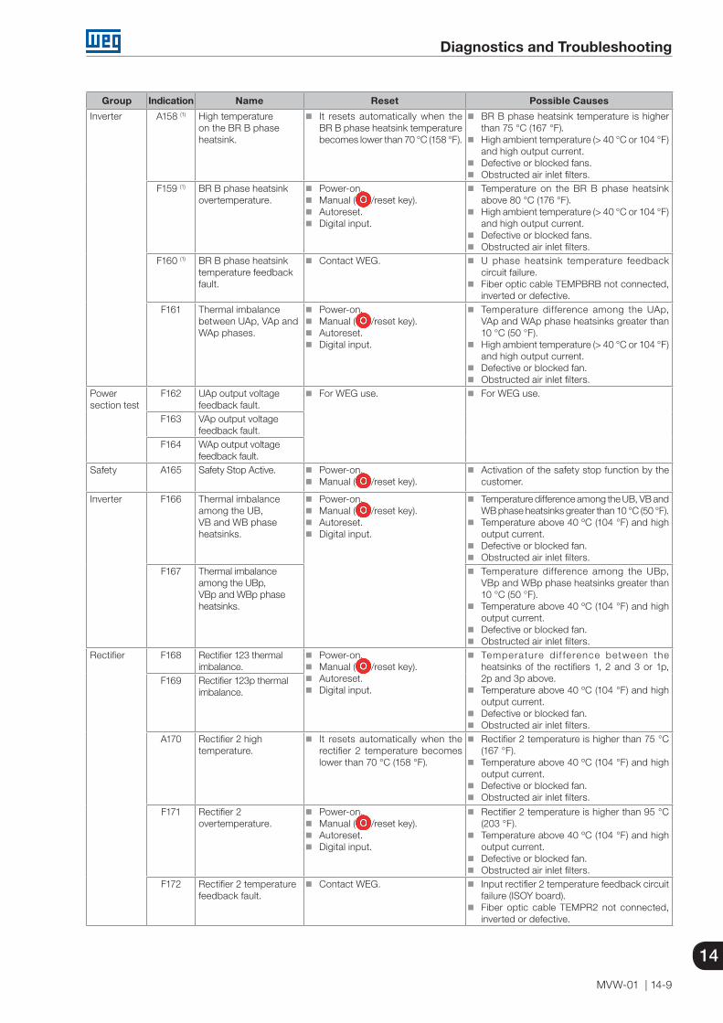
Diagnostics and Troubleshooting
MVW-01 | 14-9
14
Group Indication Name Reset Possible Causes
Inverter A158 (1) High temperature on the BR B phase heatsink.
It resets automatically when the BR B phase heatsink temperature becomes lower than 70 °C (158 °F).
BR B phase heatsink temperature is higher than 75 °C (167 °F).
High ambient temperature (> 40 °C or 104 °F) and high output current.
Defective or blocked fans. Obstructed air inlet filters.
F159 (1) BR B phase heatsinkovertemperature.
Power-on. Manual ( /reset key). Autoreset. Digital input.
Temperature on the BR B phase heatsink above 80 °C (176 °F).
High ambient temperature (> 40 °C or 104 °F) and high output current.
Defective or blocked fans. Obstructed air inlet filters.
F160 (1) BR B phase heatsinktemperature feedbackfault.
Contact WEG. U phase heatsink temperature feedback circuit failure.
Fiber optic cable TEMPBRB not connected, inverted or defective.
F161 Thermal imbalancebetween UAp, VAp andWAp phases.
Power-on. Manual ( /reset key). Autoreset. Digital input.
Temperature difference among the UAp, VAp and WAp phase heatsinks greater than 10 °C (50 °F).
High ambient temperature (> 40 °C or 104 °F) and high output current.
Defective or blocked fan. Obstructed air inlet filters.
Powersection test
F162 UAp output voltagefeedback fault.
For WEG use. For WEG use.
F163 VAp output voltagefeedback fault.
F164 WAp output voltagefeedback fault.
Safety A165 Safety Stop Active. Power-on. Manual ( /reset key).
Activation of the safety stop function by the customer.
Inverter F166 Thermal imbalanceamong the UB,VB and WB phaseheatsinks.
Power-on. Manual ( /reset key). Autoreset. Digital input.
Temperature difference among the UB, VB and WB phase heatsinks greater than 10 °C (50 °F).
Temperature above 40 ºC (104 °F) and high output current.
Defective or blocked fan. Obstructed air inlet filters.
F167 Thermal imbalanceamong the UBp,VBp and WBp phaseheatsinks.
Temperature difference among the UBp, VBp and WBp phase heatsinks greater than 10 °C (50 °F).
Temperature above 40 ºC (104 °F) and high output current.
Defective or blocked fan. Obstructed air inlet filters.
Rectifier F168 Rectifier 123 thermalimbalance.
Power-on. Manual ( /reset key). Autoreset. Digital input.
Temperature d i f fe rence between the heatsinks of the rectifiers 1, 2 and 3 or 1p, 2p and 3p above.
Temperature above 40 ºC (104 °F) and high output current.
Defective or blocked fan. Obstructed air inlet filters.
F169 Rectifier 123p thermalimbalance.
A170 Rectifier 2 hightemperature.
It resets automatically when the rectifier 2 temperature becomes lower than 70 °C (158 °F).
Rectifier 2 temperature is higher than 75 °C (167 °F).
Temperature above 40 ºC (104 °F) and high output current.
Defective or blocked fan. Obstructed air inlet filters.
F171 Rectifier 2overtemperature.
Power-on. Manual ( /reset key). Autoreset. Digital input.
Rectifier 2 temperature is higher than 95 °C (203 °F).
Temperature above 40 ºC (104 °F) and high output current.
Defective or blocked fan. Obstructed air inlet filters.
F172 Rectifier 2 temperaturefeedback fault.
Contact WEG. Input rectifier 2 temperature feedback circuit failure (ISOY board).
Fiber optic cable TEMPR2 not connected, inverted or defective.
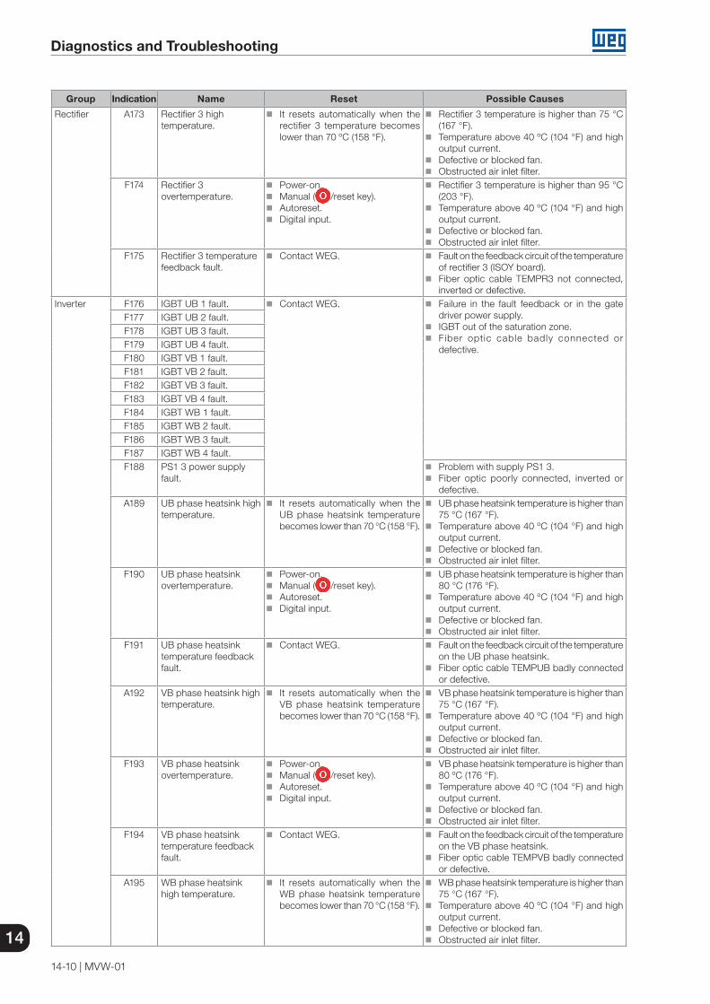
Diagnostics and Troubleshooting
14-10 | MVW-01
14
Group Indication Name Reset Possible Causes
Rectifier A173 Rectifier 3 hightemperature.
It resets automatically when the rectifier 3 temperature becomes lower than 70 ºC (158 °F).
Rectifier 3 temperature is higher than 75 °C (167 °F).
Temperature above 40 ºC (104 °F) and high output current.
Defective or blocked fan. Obstructed air inlet filter.
F174 Rectifier 3overtemperature.
Power-on. Manual ( /reset key). Autoreset. Digital input.
Rectifier 3 temperature is higher than 95 °C (203 °F).
Temperature above 40 ºC (104 °F) and high output current.
Defective or blocked fan. Obstructed air inlet filter.
F175 Rectifier 3 temperaturefeedback fault.
Contact WEG. Fault on the feedback circuit of the temperature of rectifier 3 (ISOY board).
Fiber optic cable TEMPR3 not connected, inverted or defective.
Inverter F176 IGBT UB 1 fault. Contact WEG. Failure in the fault feedback or in the gate driver power supply.
IGBT out of the saturation zone. Fiber optic cable badly connected or
defective.
F177 IGBT UB 2 fault.F178 IGBT UB 3 fault.F179 IGBT UB 4 fault.F180 IGBT VB 1 fault.F181 IGBT VB 2 fault.F182 IGBT VB 3 fault.F183 IGBT VB 4 fault.F184 IGBT WB 1 fault.F185 IGBT WB 2 fault.F186 IGBT WB 3 fault.F187 IGBT WB 4 fault.F188 PS1 3 power supply
fault. Problem with supply PS1 3. Fiber optic poorly connected, inverted or
defective.A189 UB phase heatsink high
temperature. It resets automatically when the
UB phase heatsink temperature becomes lower than 70 °C (158 °F).
UB phase heatsink temperature is higher than 75 °C (167 °F).
Temperature above 40 ºC (104 °F) and high output current.
Defective or blocked fan. Obstructed air inlet filter.
F190 UB phase heatsinkovertemperature.
Power-on. Manual ( /reset key). Autoreset. Digital input.
UB phase heatsink temperature is higher than 80 °C (176 °F).
Temperature above 40 ºC (104 °F) and high output current.
Defective or blocked fan. Obstructed air inlet filter.
F191 UB phase heatsink temperature feedback fault.
Contact WEG. Fault on the feedback circuit of the temperature on the UB phase heatsink.
Fiber optic cable TEMPUB badly connected or defective.
A192 VB phase heatsink hightemperature.
It resets automatically when the VB phase heatsink temperature becomes lower than 70 °C (158 °F).
VB phase heatsink temperature is higher than 75 °C (167 °F).
Temperature above 40 ºC (104 °F) and high output current.
Defective or blocked fan. Obstructed air inlet filter.
F193 VB phase heatsinkovertemperature.
Power-on. Manual ( /reset key). Autoreset. Digital input.
VB phase heatsink temperature is higher than 80 ºC (176 °F).
Temperature above 40 ºC (104 °F) and high output current.
Defective or blocked fan. Obstructed air inlet filter.
F194 VB phase heatsink temperature feedback fault.
Contact WEG. Fault on the feedback circuit of the temperature on the VB phase heatsink.
Fiber optic cable TEMPVB badly connected or defective.
A195 WB phase heatsinkhigh temperature.
It resets automatically when the WB phase heatsink temperature becomes lower than 70 °C (158 °F).
WB phase heatsink temperature is higher than 75 °C (167 °F).
Temperature above 40 ºC (104 °F) and high output current.
Defective or blocked fan. Obstructed air inlet filter.
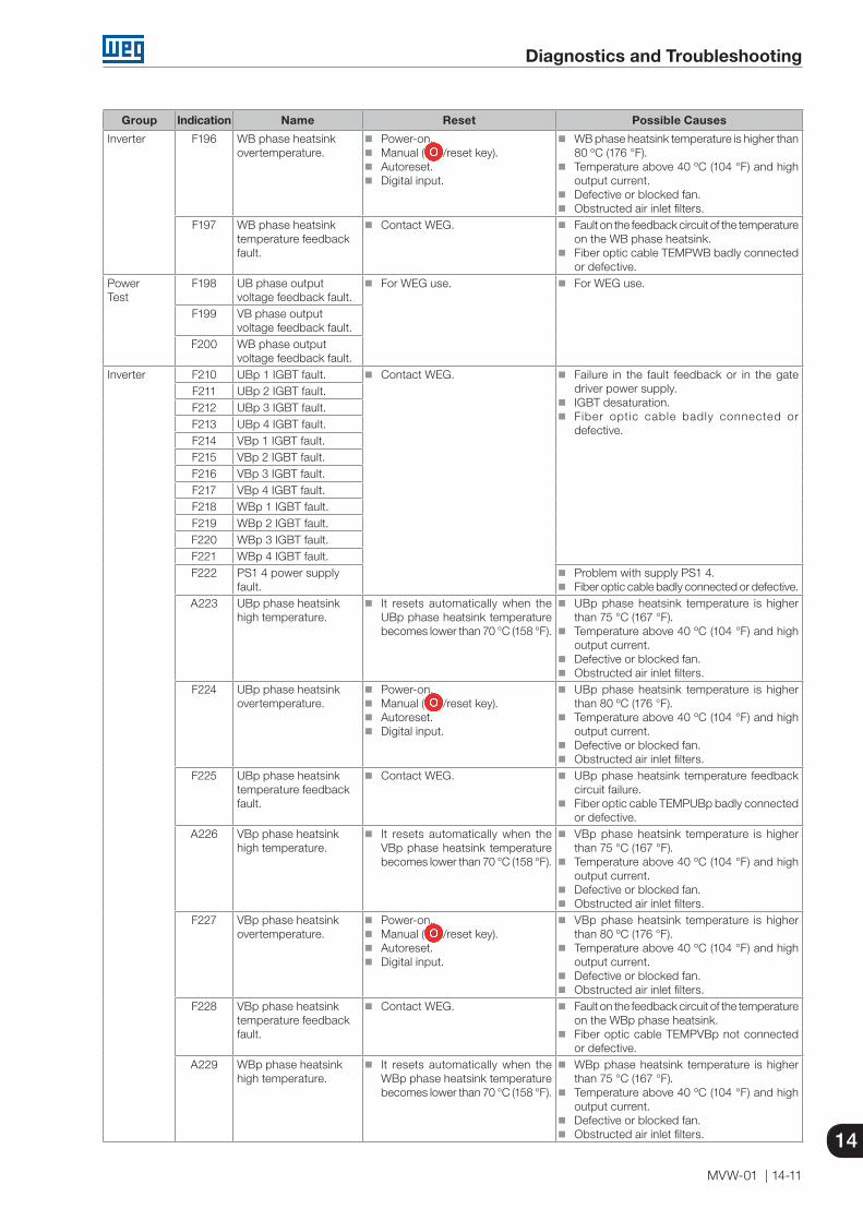
Diagnostics and Troubleshooting
MVW-01 | 14-11
14
Group Indication Name Reset Possible Causes
Inverter F196 WB phase heatsinkovertemperature.
Power-on. Manual ( /reset key). Autoreset. Digital input.
WB phase heatsink temperature is higher than 80 ºC (176 °F).
Temperature above 40 ºC (104 °F) and high output current.
Defective or blocked fan. Obstructed air inlet filters.
F197 WB phase heatsink temperature feedback fault.
Contact WEG. Fault on the feedback circuit of the temperature on the WB phase heatsink.
Fiber optic cable TEMPWB badly connected or defective.
PowerTest
F198 UB phase outputvoltage feedback fault.
For WEG use. For WEG use.
F199 VB phase outputvoltage feedback fault.
F200 WB phase outputvoltage feedback fault.
Inverter F210 UBp 1 IGBT fault. Contact WEG. Failure in the fault feedback or in the gate driver power supply.
IGBT desaturation. Fiber optic cable badly connected or
defective.
F211 UBp 2 IGBT fault.F212 UBp 3 IGBT fault.F213 UBp 4 IGBT fault.F214 VBp 1 IGBT fault. F215 VBp 2 IGBT fault. F216 VBp 3 IGBT fault. F217 VBp 4 IGBT fault. F218 WBp 1 IGBT fault. F219 WBp 2 IGBT fault. F220 WBp 3 IGBT fault. F221 WBp 4 IGBT fault. F222 PS1 4 power supply
fault. Problem with supply PS1 4. Fiber optic cable badly connected or defective.
A223 UBp phase heatsinkhigh temperature.
It resets automatically when the UBp phase heatsink temperature becomes lower than 70 °C (158 °F).
UBp phase heatsink temperature is higher than 75 °C (167 °F).
Temperature above 40 ºC (104 °F) and high output current.
Defective or blocked fan. Obstructed air inlet filters.
F224 UBp phase heatsinkovertemperature.
Power-on. Manual ( /reset key). Autoreset. Digital input.
UBp phase heatsink temperature is higher than 80 ºC (176 °F).
Temperature above 40 ºC (104 °F) and high output current.
Defective or blocked fan. Obstructed air inlet filters.
F225 UBp phase heatsink temperature feedback fault.
Contact WEG. UBp phase heatsink temperature feedback circuit failure.
Fiber optic cable TEMPUBp badly connected or defective.
A226 VBp phase heatsinkhigh temperature.
It resets automatically when the VBp phase heatsink temperature becomes lower than 70 °C (158 °F).
VBp phase heatsink temperature is higher than 75 °C (167 °F).
Temperature above 40 ºC (104 °F) and high output current.
Defective or blocked fan. Obstructed air inlet filters.
F227 VBp phase heatsinkovertemperature.
Power-on. Manual ( /reset key). Autoreset. Digital input.
VBp phase heatsink temperature is higher than 80 ºC (176 °F).
Temperature above 40 ºC (104 °F) and high output current.
Defective or blocked fan. Obstructed air inlet filters.
F228 VBp phase heatsink temperature feedback fault.
Contact WEG. Fault on the feedback circuit of the temperature on the WBp phase heatsink.
Fiber optic cable TEMPVBp not connected or defective.
A229 WBp phase heatsinkhigh temperature.
It resets automatically when the WBp phase heatsink temperature becomes lower than 70 °C (158 °F).
WBp phase heatsink temperature is higher than 75 °C (167 °F).
Temperature above 40 ºC (104 °F) and high output current.
Defective or blocked fan. Obstructed air inlet filters.

Diagnostics and Troubleshooting
14-12 | MVW-01
14
Group Indication Name Reset Possible Causes
Inverter F230 WBp phase heatsinkovertemperature.
Power-on. Manual ( /reset key). Autoreset. Digital input.
WBp phase heatsink temperature is higher than 80 ºC (176 °F).
Temperature above 40 ºC (104 °F) and high output current.
Defective or blocked fan. Obstructed air inlet filters.
F231 WBp phase heatsink temperature feedback fault.
Contact WEG. Fault on the feedback circuit of the temperature on the WBp phase heatsink.
Fiber optic cable TEMPWBp not connected or defective.
PowerTest
F232 UBp phase outputvoltage feedback fault.
For WEG use. For WEG use.
F233 VBp phase outputvoltage feedback fault.
F234 WBp phase outputvoltage feedback fault.
DC Link F236 V DC link imbalance. Power-on. Manual ( /reset key). Autoreset. Digital input.
The voltage difference between positive and negative links is greater than 15 % of the nominal value.
Fiber optic cables VPV1 or VNV1 badly connected.
F237 W DC link imbalance. The voltage difference between positive and negative links is greater than 15 % of the nominal value.
Fiber optic cables VPW1 or VNW1 badly connected.
F238 V DC link overvoltage (Positive or Negative).
The power supply voltage is too high producing a DC link voltage higher than 130 % of the nominal value.
The deceleration ramp is too fast.F239 W DC link overvoltage
(Positive or Negative). The power supply voltage is too high producing
a DC link voltage higher than 130 % of the nominal value.
The deceleration ramp is too fast.
14.2 INFORMATION FOR CONTACTING TECHNICAL SUPPORT
NOTE!For technical support or service request, it is important to have the following data available:
Inverter model. Serial number, manufacturing date and hardware revision, which are available on the product
identification label (refer to the Section 1.3 MVW-01 IDENTIFICATION LABEL on page 1-2). Software version (refer to the Section 2.2 SOFTWARE VERSION on page 2-1). Application and Programming data.
For explanations, training or services, please, contact WEG Technical Assistance.
14.3 PREVENTIVE MAINTENANCE
DANGER! Only trained personnel, with proper qualifications, and familiar with the MVW-01 and associated
equipment shall plan and implement the installation, starting, operation, and maintenance of this equipment.
These personnel shall follow all the safety instructions described in this manual and/or defined by local regulations.
Failure to comply with the safety instructions may result in death, serious injury, and/or equipment damage.
WEG Technical Assistance.
Diagnostics and Troubleshooting
MVW-01 | 14-13
14
DANGER! Seul un personnel formé, ayant les qualifications adéquates et familiarisé avec le MVW-01 et
l’équipement associé peut planifier et mettre en oeuvre l’installation, le démarrage, l’utilisation et la maintenance de cet équipement.
Ce personnel doit suivre toutes les instructions de sécurité décrites dans ce mode d’emploi et/ou définies par la règlementation locale.
Le non-respect de ces instructions de sécurité peut entraîner la mort, de graves blessures et/ou des dommages aux équipements.
WEG l'Assistance Technique.
The MVW-01 inverter has been designed and tested to have a long, failure-free, operation life. The preventive maintenance helps early identification of possible future failures, extending the useful life of the equipment, increasing the mean time between failures and reducing the stopped equipment time. It also helps identifying whether the equipment is being used within its mechanical, electrical and environmental limits. The periodical cleaning during preventive maintenance assures an adequate operation when the inverter is used within its rated conditions.
In order to produce the best benefits, the preventive maintenance must be performed periodically by a qualified technician. The interval depends on factors like the duty cycle and the environmental conditions (ambient temperature, ventilation, the existence of dust, etc.). It is recommended to begin with the preventive maintenance frequently and increase the interval as the obtained results indicate the possibility of reducing that frequency. A detailed record of the preventive maintenance is also recommended. These records serve as proof of the maintenance fulfillment and facilitate the identification of possible faults and alarms.
Two types of preventive maintenance are described next, during the operation of the equipment and with the complete stop/de-energization of the inverter.
14.3.1 Preventive Maintenance During the Operation
This type of maintenance is performed with the inverter energized and in operation. There is necessary access onlyto the control cabinet where low voltage supply voltages (< 480 V) are present, but which are potentially dangerous.
DANGER! This equipment has high voltages that may cause electric shocks. Only qualified personnel
familiar with the MVW-01 frequency Inverter and associated equipment should plan or implement the maintenance of this equipment. In order to avoid risk of electric shock, follow all the safety procedures required for service on energized equipment.
Do not touch any electric circuit before making sure it is de-energized.
DANGER! Seul un personnel formé, ayant les qualifications adéquates et familiarisé avec le MVW-01 et
l’équipement associé peut planifier et mettre en oeuvre l’installation, le démarrage, l’utilisation et la maintenance de cet équipement. Ce personnel doit suivre toutes les instructions de sécurité décrites dans ce mode d’emploi et/ou définies par la règlementation locale.
Le non-respect de ces instructions de sécurité peut entraîner la mort, de graves blessures et/ou des dommages aux équipements.
Procedures:1. Operation of the fans and exhausting fans: Verify the proper operation of the exhausting fans at the top of the rectifier cabinet and the inverter cabinet. The fans must be running in the same direction and their exhausting action must be perceptible. Verify the proper operation of the fan at the control cabinet. It must be running and blowing air into the cabinet.

Diagnostics and Troubleshooting
14-14 | MVW-01
14
2. Cleaning of the air inlet filters: Remove the protection grids from the air inlets at the doors of all the cabinets by unbolting them. Remove the
filters and clean, wash or replace them. The amount of accumulated dirt on the filters helps defining the correct interval between preventing maintenances. Reinstall the filters and bolt the protection grids again.
3. Open the control cabinet and visually inspect the components inside it, verifying them to identify faults or the need of preventive maintenance with complete stop/de-energization for cleaning or replacement:
Table 14.2: Visually inspect
Components Anomalies
Electronic boards.Excessive dust, oil, moisture, etc. accumulation. Discolored or darker points, due to excessive heat.
Capacitors on electronic boards. Discoloration, smell, electrolyte leakage, case deformation.Resistors in general. Discoloration or smell.
Control rack (A8), electronics powersupply PS24 (A11).
Excessive heating of the aluminum base (more than 40 °C, 104 °F, above the ambient temperature).
4. Read and write down the following from the HMI, P003 - Motor Current, P004 - DC Link Voltage, P005 - Motor Frequency, P006 - Inverter Status, P014 to P017 Last to Fourth Error (get access to the details of each error by pressing the key on the HMI while the parameter is selected), P022 - MVC3 Board Temperature, P042 - Powered Time, P043 - Enabled Time, P055 - U Phase Power Arm Temperature, P056 - V Phase Power Arm Temperature, P057 - W Phase Power Arm Temperature, P058 - Braking Arm Temperature, P059 - Rectifier Temperature, P080 - Date and P081 - Time.
14.3.2 Preventive Maintenance with Complete Stop/De-energization
DANGER! This equipment has high voltages that may cause electric shocks. Only qualified personnel
familiar with the MVW-01 frequency Inverter and associated equipment should plan or implement the maintenance of this equipment. In order to avoid risk of electric shock, follow all the safety procedures required for service on energized equipment.
Do not touch any electric circuit before making sure it is de-energized.
DANGER! Cet équipement a des tensions élevées pouvant causer des décharges électriques. Seul un
personnel qualifié et familier avec l’onduleur de fréquence MVW-01 et ses équipements associés doit préparer et mettre en oeuvre l’entretien de cet équipement. Afin d’éviter un risque de décharge électrique, suivez toutes les procédures de sécurité requises pour l’entretien courant sur un équipement sous tension.
Ne touchez aucun circuit électrique avant de vous être assuré qu’il est hors tension.
This type of maintenance is also destined for the cleaning and visual inspection of the high voltage cabinets; therefore, it requires the complete de-energization of the inverter. It can be less frequent than the maintenance during operation.
Procedures:1. Execute the procedures from 1 and 4, of the Preventive Maintenance During Operation.
DANGER!Although the inverter commands the opening of the input circuit breaker, there is no guarantee of its opening and neither that no voltages are present, because the capacitors remain charged for a long time and they can also be charged through the auxiliary low voltage supply. Before opening and accessing the medium voltage cabinets, follow all the safe de-energization procedures described next.
Diagnostics and Troubleshooting
MVW-01 | 14-15
14
DANGER!Bien que l’onduleur commande l’ouverture du coupe-circuit d’entrée, il n’y a aucune garantie qu’il s’ouvrira ni qu’aucune tension n’est présente, car les condensateurs restent chargés pendant longtemps et ils peuvent également être chargés par l’alimentation basse tension auxiliaire. Avant d’ouvrir et d’accéder aux armoires moyenne tension moyenne, suivez toutes les procédures de mise hors tension de sécurité décrites ci-dessous.
14.4 SAFE DE-ENERGIZATION INSTRUCTIONS
1. Decelerate the motor to a complete stop.
2. Check the DC link voltage at the parameter P004 on the HMI. Open the control panel door and locate the neon lamps of the HVM (High Voltage Monitoring board), mounted on the cabinet left side. The four lamps must be on if the voltage showed via P004 is above 200 V.
3. Press the “POWER OFF” pushbutton. The input transformer circuit breaker is switched off at this moment, and the “INPUT ON” pilot light going off indicates it.
ATTENTION!If the input transformer circuit breaker does not open with the “POWER OFF” command, then open it manually.
4. Follow the DC link voltage decrease through P004 on the HMI and the HVM neon lamps. When the DC link voltage crosses below 200 V the neon lamps start flashing with progressively lower frequency until going off completely. Wait until the DC link voltage displayed at P004 on the HMI gets below 25 V.
5. At the input transformer circuit breaker cubicle, extract the circuit breaker from its operation position and close the transformer primary winding grounding switch. Lock the cubicle with the key and/or put a warning sign "System in maintenance".
6. Press the emergency pushbutton located on the control column door and remove its key.
7. Switch off the Q2 circuit breaker in the control column and lock it in the open position with a padlock and/or put a warning sign "System in maintenance".
8. Switch off the Q1 circuit breaker in the control column. Remove the auxiliary power supply.
It is only after the sequence of procedures described here that medium voltage compartment doors can be opened.
DANGER!If it were not possible to follow the discharge of the DC link capacitors through the parameter P004, as well as through the HVM board neon lamps, due to a malfunction or a previous, de-energization, follow the instructions 5 through 8 and wait 10 minutes more.
DANGER!S’il n’était pas possible de suivre la décharge des condensateurs de liaison CC avec le paramètre P004 et les lampes à néon de la carte HVM en raison d’un dysfonctionnement ou une mise hors tension préalable, suivez les instructions 5 jusqu’à 8 et attendez 10 minutes supplémentaires.
9. Execute the procedures 2 and 3 of the Preventive Maintenance During Operation.
10. Clean the dust accumulated in the interior of the control and medium voltage cabinets as described next:
Heatsink ventilation system (fans, rectifier and inverter arm heatsinks): remove the dust accumulated on the heatsink fins using compressed air.
Diagnostics and Troubleshooting
14-16 | MVW-01
14
Electronic boards: remove the dust accumulated on the boards using a anti-static brush and/ or low pressure ionized compressed air. If necessary, remove the boards from the inverter.
ATTENTION!Electronic boards have components sensitive to electrostatic discharges. Do not touch directly on components or connectors. If necessary, touch the grounded metallic frame first or use an adequate grounded wrist strap.
Cabinet inner part and other components: remove the accumulated dust using an vacuum cleaner with a nonmetallic nozzle. Perform this cleaning especially on the insulating materials that support energized parts, to avoid leakage currents during the operation.
11. Connection retightening: inspect all the electrical and mechanical connections and retighten them if necessary.
12. Reinstall all the removed components and connections in their respective places and follow the start-up procedures described in the Section 8.3 ENERGIZATION, START-UP AND SAFE DE-ENERGIZATION on page 8-17.
14.5 GENERAL WARRANTY CONDITIONS FOR MVW-01 FREQUENCY INVERTERS
Weg Automação S.A, located at Av. Pref. Waldemar Grubba, 3000 in the city of Jaraguá do Sul – SC, provides warranty for defects in material and workmanship for WEG frequency inverters under the following conditions:
1.0 For the effectiveness of this warranty, it is essential that the buyer carefully inspects the purchased inverter immediately after its delivery, checking thoroughly its characteristics and installation, setting, operation and maintenance instructions. The inverter will be automatically considered as accepted and approved by the buyer when no written notice is given by the buyer within at most 5 days after the delivery date.
2.0 The total length of this warranty is of twelve months from the date of the supply by WEG or authorized dealer, proven through the purchase invoice of the equipment, and limited to twenty four months from the product manufacturing date, which is stated on the label attached to the product.
3.0 In case the inverter under warranty does not work properly or does not work at all, the warranty services may be performed during the business hours at WEG’s sole discretion, at its headquarters in Jaraguá do Sul - SC, or at an Authorized Service Provider assigned by Weg Automation.
4.0 The defective product must be available to the supplier for the required period to detect the cause of the failure and to perform the corresponding repairs.
5.0 Weg Automação or an Authorized Service Provider will analyze the returned product, and, if any fault covered under the warranty is observed, they will repair, modify or replace the defective inverter at their own discretion, at not costs to the buyer, except as indicated in Chapter 14 DIAGNOSTICS AND TROUBLESHOOTING on page 14-1.
6.0 The responsibility for this warranty is limited exclusively to the repair, modification or replacement of the inverter supplied. Weg takes no liabilities for personal injuries, damages to third parties, other equipment or installations, loss of profits, or any other incidental or consequential damages.
7.0 Other expenses, such as freights, packaging, disassembly/assembly and parameterization costs, will be paid exclusively by the buyer, including all working hours, transportation/accommodation and meal expenses for technical personnel, when service is needed and/or requested at the costumer’s premises.
8.0 This warranty neither covers the normal wear of the product or equipment, nor damages resulting from incorrect or negligent operation, incorrect parameterization, improper maintenance or storage, abnormal operation in disagreement with the technical specifications, poor quality installations, or any influence of chemical, electrochemical, electrical, mechanical or atmospheric nature.
Related Documents