M.E. – VLSI Design MISSION OF THE DEPARTMENT To provide excellence through effective and qualitative teaching- learning process that equips the students with adequate knowledge and to transform the students’ lives by nurturing the human values to serve as a precious resource for Electronics and Communication Engineering and nation. To enhance the problem solving and lifelong learning skills that will enable by edifying the students to pursue higher studies and career in research. To create students with effective communication skills, the abilities to lead ethical values in order to fulfill the social needs Curriculum and Syllabi 2021 – PG CHOICE BASED CREDIT SYSTEM AND OBE VISION OF THE DEPARTMENT To develop Electronics and Communication Engineers by permeating with proficient morals, to be recognized as an adroit engineer worldwide and to strive endlessly for excellence to meet the confronts of our modern society by equipping them with changing technologies, professionalism, creativity research, employability, analytical, practical skills and to excel as a successful entrepreneur.

Welcome message from author
This document is posted to help you gain knowledge. Please leave a comment to let me know what you think about it! Share it to your friends and learn new things together.
Transcript
M.E. – VLSI Design
MISSION OF THE DEPARTMENT
To provide excellence through effective and qualitative teaching- learning
process that equips the students with adequate knowledge and to transform the
students’ lives by nurturing the human values to serve as a precious resource for
Electronics and Communication Engineering and nation.
To enhance the problem solving and lifelong learning skills that will enable by
edifying the students to pursue higher studies and career in research.
To create students with effective communication skills, the abilities to lead
ethical values in order to fulfill the social needs
Curriculum and Syllabi 2021 – PG
CHOICE BASED CREDIT SYSTEM AND OBE
VISION OF THE DEPARTMENT
To develop Electronics and Communication Engineers by permeating with
proficient morals, to be recognized as an adroit engineer worldwide and to strive
endlessly for excellence to meet the confronts of our modern society by equipping
them with changing technologies, professionalism, creativity research,
employability, analytical, practical skills and to excel as a successful entrepreneur.
Francis Xavier Engineering College | Department of ECE |M.E-VLSI | R2019 | Curriculum and Syllabi 2021 2
Table of Contents
S.No Contents Page No
1 Vision And Mission Of Department 1
2 Program Educational Objectives 3
3 Programme Specific Outcomes 3
4 Programme Outcomes 3
5 Mapping With PO Vs PEO, PSO 5
6 Credit Distribution 6
7 Subject List 7
8 Syllabus of individual subjects 11
Francis Xavier Engineering College | Department of ECE |M.E-VLSI | R2019 | Curriculum and Syllabi 2021 3
FRANCIS XAVIER ENGINEERING COLLEGE, TIRUNELVELI
DEPARTMENT OF ELECTRONICIS AND COMMUNICATION ENGINEERING
103 G2 Bye Pass Road, Vannarpettai, Tirunelveli, Tamilnadu – 627003
Phone : 0462 – 2502283, 2502157, Fax: 0462 – 2501007
Email :[email protected], Website : www. francisxavier.ac.in
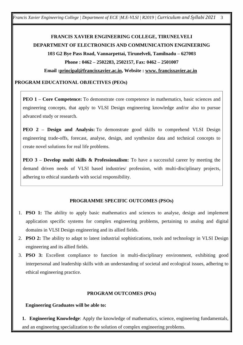
PROGRAM EDUCATIONAL OBJECTIVES (PEOs)
PEO 1 – Core Competence: To demonstrate core competence in mathematics, basic sciences and
engineering concepts, that apply to VLSI Design engineering knowledge and/or also to pursue
advanced study or research.
PEO 2 – Design and Analysis: To demonstrate good skills to comprehend VLSI Design
engineering trade-offs, forecast, analyse, design, and synthesize data and technical concepts to
create novel solutions for real life problems.
PEO 3 – Develop multi skills & Professionalism: To have a successful career by meeting the
demand driven needs of VLSI based industries/ profession, with multi-disciplinary projects,
adhering to ethical standards with social responsibility.
PROGRAMME SPECIFIC OUTCOMES (PSOs)
2. PSO 2: The ability to adapt to latest industrial sophistications, tools and technology in VLSI Design
engineering and its allied fields.
3. PSO 3: Excellent compliance to function in multi-disciplinary environment, exhibiting good
interpersonal and leadership skills with an understanding of societal and ecological issues, adhering to
ethical engineering practice.
PROGRAM OUTCOMES (POs)
Engineering Graduates will be able to:
1. Engineering Knowledge: Apply the knowledge of mathematics, science, engineering fundamentals,
and an engineering specialization to the solution of complex engineering problems.
1. PSO 1: The ability to apply basic mathematics and sciences to analyse, design and implement
application specific systems for complex engineering problems, pertaining to analog and digital
domains in VLSI Design engineering and its allied fields.
Francis Xavier Engineering College | Department of ECE |M.E-VLSI | R2019 | Curriculum and Syllabi 2021 4
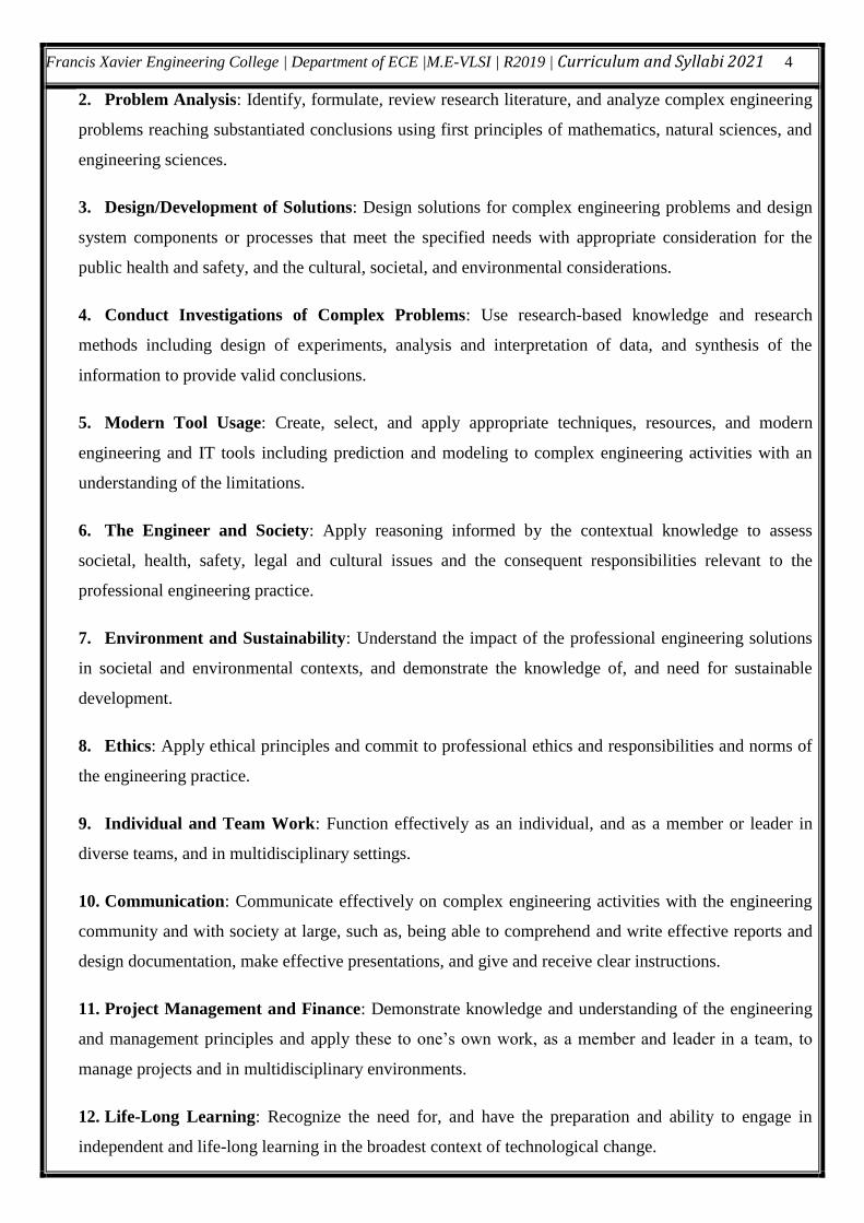
2. Problem Analysis: Identify, formulate, review research literature, and analyze complex engineering
problems reaching substantiated conclusions using first principles of mathematics, natural sciences, and
engineering sciences.
3. Design/Development of Solutions: Design solutions for complex engineering problems and design
system components or processes that meet the specified needs with appropriate consideration for the
public health and safety, and the cultural, societal, and environmental considerations.
4. Conduct Investigations of Complex Problems: Use research-based knowledge and research
methods including design of experiments, analysis and interpretation of data, and synthesis of the
information to provide valid conclusions.
5. Modern Tool Usage: Create, select, and apply appropriate techniques, resources, and modern
engineering and IT tools including prediction and modeling to complex engineering activities with an
understanding of the limitations.
6. The Engineer and Society: Apply reasoning informed by the contextual knowledge to assess
societal, health, safety, legal and cultural issues and the consequent responsibilities relevant to the
professional engineering practice.
7. Environment and Sustainability: Understand the impact of the professional engineering solutions
in societal and environmental contexts, and demonstrate the knowledge of, and need for sustainable
development.
8. Ethics: Apply ethical principles and commit to professional ethics and responsibilities and norms of
the engineering practice.
9. Individual and Team Work: Function effectively as an individual, and as a member or leader in
diverse teams, and in multidisciplinary settings.
10. Communication: Communicate effectively on complex engineering activities with the engineering
community and with society at large, such as, being able to comprehend and write effective reports and
design documentation, make effective presentations, and give and receive clear instructions.
11. Project Management and Finance: Demonstrate knowledge and understanding of the engineering
and management principles and apply these to one’s own work, as a member and leader in a team, to
manage projects and in multidisciplinary environments.
12. Life-Long Learning: Recognize the need for, and have the preparation and ability to engage in
independent and life-long learning in the broadest context of technological change.
Francis Xavier Engineering College | Department of ECE |M.E-VLSI | R2019 | Curriculum and Syllabi 2021 5
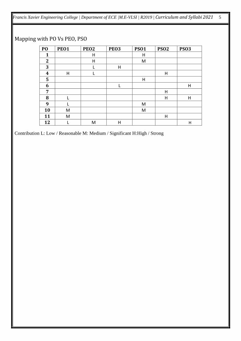
Mapping with PO Vs PEO, PSO
PO PEO1 PEO2 PEO3 PSO1 PSO2 PSO3 1 H H
2 H M
3 L H
4 H L H
5 H
6 L H
7 H
8 L H H
9 L M
10 M M
11 M H 12 L M H H
Contribution L: Low / Reasonable M: Medium / Significant H:High / Strong
Francis Xavier Engineering College | Department of ECE |M.E-VLSI | R2019 | Curriculum and Syllabi 2021 6
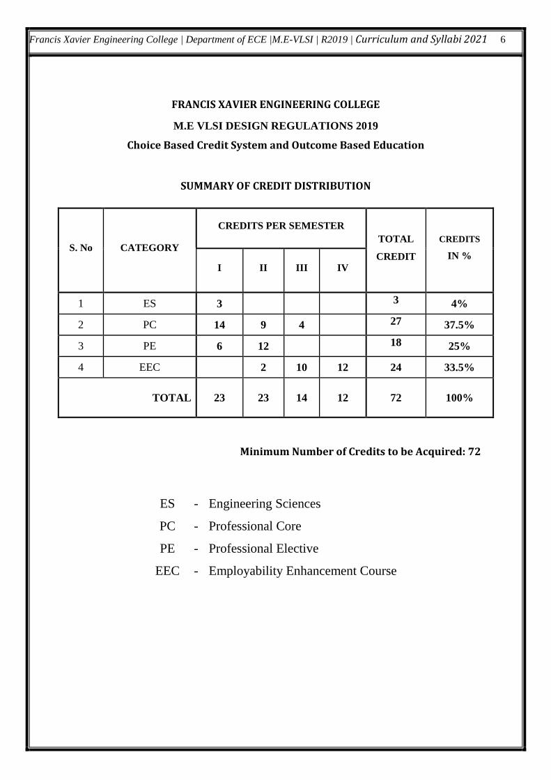
FRANCIS XAVIER ENGINEERING COLLEGE
M.E VLSI DESIGN REGULATIONS 2019
Choice Based Credit System and Outcome Based Education
SUMMARY OF CREDIT DISTRIBUTION
Minimum Number of Credits to be Acquired: 72
ES - Engineering Sciences
PC - Professional Core
PE - Professional Elective
EEC - Employability Enhancement Course
S. No CATEGORY
CREDITS PER SEMESTER
TOTAL
CREDIT
CREDITS
IN %
I II III IV
1 ES 3
3 4%
2 PC 14 9 4
27 37.5%
3 PE 6 12
18 25%
4 EEC
2 10 12 24 33.5%
TOTAL
23 23 14 12 72 100%
Francis Xavier Engineering College | Department of ECE |M.E-VLSI | R2019 | Curriculum and Syllabi 2021 7
FRANCIS XAVIER ENGINEERING COLLEGE
M.E VLSI DESIGN REGULATIONS 2019
Choice Based Credit System and Outcome Based Education
I – IV Semesters Curricula and Syllabi 2021
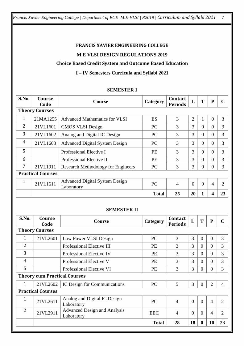
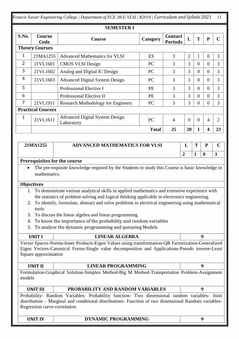
SEMESTER I
S.No. Course Code
Course Category Contact Periods
L T P C
Theory Courses
1 21MA1255 Advanced Mathematics for VLSI ES 3 2 1 0 3
2 21VL1601 CMOS VLSI Design PC 3 3 0 0 3
3 21VL1602 Analog and Digital IC Design PC 3 3 0 0 3
4 21VL1603 Advanced Digital System Design PC 3 3 0 0 3
5 Professional Elective I PE 3 3 0 0 3
6 Professional Elective II PE 3 3 0 0 3
7 21VL1911 Research Methodology for Engineers PC 3 3 0 0 3
Practical Courses
1 21VL1611
Advanced Digital System Design
Laboratory PC 4 0 0 4 2
Total 25 20 1 4 23
SEMESTER II
S.No. Course Code
Course Category Contact Periods
L T P C
Theory Courses
1 21VL2601 Low Power VLSI Design PC 3 3 0 0 3
2 Professional Elective III PE 3 3 0 0 3
3 Professional Elective IV PE 3 3 0 0 3
4 Professional Elective V PE 3 3 0 0 3
5 Professional Elective VI PE 3 3 0 0 3
Theory cum Practical Courses
1 21VL2602 IC Design for Communications PC 5 3 0 2 4
Practical Courses
1 21VL2611
Analog and Digital IC Design
Laboratory PC 4 0 0 4 2
2 21VL2911
Advanced Design and Analysis
Laboratory EEC 4 0 0 4 2
Total 28 18 0 10 23
Francis Xavier Engineering College | Department of ECE |M.E-VLSI | R2019 | Curriculum and Syllabi 2021 8
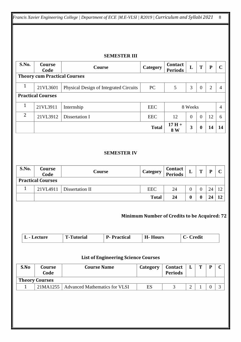
SEMESTER III
S.No. Course Code
Course Category Contact Periods
L T P C
Theory cum Practical Courses
1 21VL3601 Physical Design of Integrated Circuits PC 5 3 0 2 4
Practical Courses
1 21VL3911 Internship EEC 8 Weeks 4
2 21VL3912 Dissertation I EEC 12 0 0 12 6
Total
17 H +
8 W 3 0 14 14
SEMESTER IV
Minimum Number of Credits to be Acquired: 72
L - Lecture T-Tutorial P- Practical H- Hours C- Credit
List of Engineering Science Courses
S.No Course Code
Course Name Category Contact Periods
L T P C
Theory Courses
1 21MA1255 Advanced Mathematics for VLSI ES 3 2 1 0 3
S.No. Course Code
Course Category Contact Periods
L T P C
Practical Courses
1 21VL4911 Dissertation II EEC 24 0 0 24 12
Total 24 0 0 24 12
Francis Xavier Engineering College | Department of ECE |M.E-VLSI | R2019 | Curriculum and Syllabi 2021 9
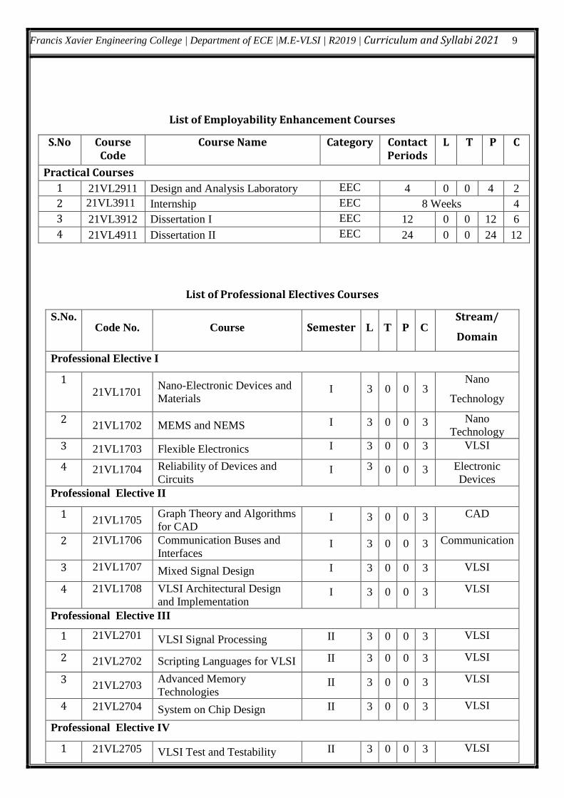
List of Employability Enhancement Courses
S.No Course Code
Course Name Category Contact Periods
L T P C
Practical Courses
1 21VL2911 Design and Analysis Laboratory EEC 4 0 0 4 2
2 21VL3911 Internship EEC 8 Weeks 4
3 21VL3912 Dissertation I EEC 12 0 0 12 6
4 21VL4911 Dissertation II EEC 24 0 0 24 12
List of Professional Electives Courses
S.No. Code No. Course Semester L T P C
Stream/
Domain
Professional Elective I
1 21VL1701
Nano-Electronic Devices and
Materials I 3 0 0 3
Nano
Technology
2 21VL1702 MEMS and NEMS I 3 0 0 3 Nano
Technology
3 21VL1703 Flexible Electronics I 3 0 0 3 VLSI
4 21VL1704 Reliability of Devices and
Circuits I 3 0 0 3 Electronic
Devices
Professional Elective II
1 21VL1705
Graph Theory and Algorithms
for CAD I 3 0 0 3 CAD
2 21VL1706 Communication Buses and
Interfaces I 3 0 0 3 Communication
3 21VL1707 Mixed Signal Design I 3 0 0 3 VLSI
4 21VL1708 VLSI Architectural Design
and Implementation I 3 0 0 3 VLSI
Professional Elective III
1 21VL2701 VLSI Signal Processing II 3 0 0 3 VLSI
2 21VL2702 Scripting Languages for VLSI II 3 0 0 3 VLSI
3 21VL2703
Advanced Memory
Technologies II 3 0 0 3 VLSI
4 21VL2704 System on Chip Design II 3 0 0 3 VLSI
Professional Elective IV
1 21VL2705 VLSI Test and Testability II 3 0 0 3 VLSI
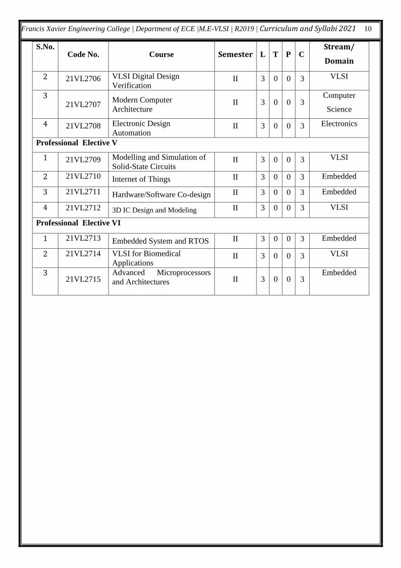
Francis Xavier Engineering College | Department of ECE |M.E-VLSI | R2019 | Curriculum and Syllabi 2021 10
S.No. Code No. Course Semester L T P C
Stream/
Domain
2 21VL2706 VLSI Digital Design
Verification II 3 0 0 3 VLSI
3 21VL2707
Modern Computer
Architecture II 3 0 0 3
Computer
Science
4 21VL2708 Electronic Design
Automation II 3 0 0 3 Electronics
Professional Elective V
1 21VL2709 Modelling and Simulation of
Solid-State Circuits II 3 0 0 3 VLSI
2 21VL2710 Internet of Things II 3 0 0 3 Embedded
3 21VL2711 Hardware/Software Co-design II 3 0 0 3 Embedded
4 21VL2712 3D IC Design and Modeling II 3 0 0 3 VLSI
Professional Elective VI
1 21VL2713 Embedded System and RTOS II 3 0 0 3 Embedded
2 21VL2714 VLSI for Biomedical
Applications II 3 0 0 3 VLSI
3 21VL2715
Advanced Microprocessors
and Architectures
II 3 0 0 3 Embedded
Francis Xavier Engineering College | Department of ECE |M.E-VLSI | R2019 | Curriculum and Syllabi 2021 11
SEMESTER I
S.No. Course Code
Course Category Contact Periods
L T P C
Theory Courses
1 21MA1255 Advanced Mathematics for VLSI ES 3 2 1 0 3
2 21VL1601 CMOS VLSI Design PC 3 3 0 0 3
3 21VL1602 Analog and Digital IC Design PC 3 3 0 0 3
4 21VL1603 Advanced Digital System Design PC 3 3 0 0 3
5 Professional Elective I PE 3 3 0 0 3
6 Professional Elective II PE 3 3 0 0 3
7 21VL1911 Research Methodology for Engineers PC 3 3 0 0 3
Practical Courses
1 21VL1611
Advanced Digital System Design
Laboratory PC 4 0 0 4 2
Total 25 20 1 4 23
21MA1255 ADVANCED MATHEMATICS FOR VLSI L T P C
2 1 0 3
Prerequisites for the course
The pre-requisite knowledge required by the Students to study this Course is basic knowledge in
mathematics.
Objectives
1. To demonstrate various analytical skills in applied mathematics and extensive experience with
the statistics of problem solving and logical thinking applicable in electronics engineering.
2. To identify, formulate, abstract and solve problems in electrical engineering using mathematical
tools 3. To discuss the linear algebra and linear programming
4. To know the importance of the probability and random variables
5. To analyse the dynamic programming and queueing Models
UNIT I LINEAR ALGEBRA 9
Vector Spaces-Norms-Inner Products-Eigen Values using transformation-QR Factorization-Generalized
Eigen Vectors-Canonical Forms-Single value decomposition and Applications-Pseudo inverse-Least
Square approximation
UNIT II LINEAR PROGRAMMING 9
Formulation-Graphical Solution-Simplex Method-Big M Method-Transportation Problem-Assignment
models
UNIT III PROBABILITY AND RANDOM VARIABLES 9
Probability- Random Variables- Probability function- Two dimensional random variables- Joint
distribution – Marginal and conditional distributions- Function of two dimensional Random variables-
Regression curve-correlation
UNIT IV DYNAMIC PROGRAMMING 9
Francis Xavier Engineering College | Department of ECE |M.E-VLSI | R2019 | Curriculum and Syllabi 2021 12
Dynamic programming- Principle of optimality- Forward and backward recursion- Applications of
Dynamic programming- Problem of dimensionality
UNIT V QUEUEING MODELS 9
Poisson process- Markovian queues- Single and Multi –server models- Little’s formula Steady state
analysis
Total Periods 45
Suggestive Assessment Methods
Continuous Assessment Test (30 Marks)
Formative Assessment Test (10 Marks)
End Semester Exams (60 Marks)
1. Description Questions 2. Formative Multiple Choice
Questions
1. Assignment 2. Online Quizzes 3. Problem Solving
Activities
1. Description Questions
2. Formative Multiple Choice Questions
Outcomes
Upon completion of the course, the students will be able to: CO255. 1 Concepts of fuzzy sets, knowledge representation using fuzzy rules, fuzzy logic,
fuzzy prepositions and fuzzy quantifiers and applications of fuzzy logic.
CO255. 2 Apply various methods in matrix theory to solve system of linear equations.
CO255. 3 Computation of probability and moments, standard distributions of discrete and
continuous random variables and functions of a random variable.
CO255. 4 Conceptualize the principle of optimality and sub-optimization, formulation and
computational procedure of dynamic programming
CO255. 5 Exposing the basic characteristic features of a queuing system and acquire skills in
analyzing queuing models.
Text Books
1. George J. Klir and Yuan, B., Fuzzy sets and fuzzy logic, Theory and applications, Prentice Hall of
India Pvt. Ltd., 1997.
2. Moon, T.K., Sterling, W.C., Mathematical methods and algorithms for signal processing, Pearson
Education, 2000
Reference Books
1. Richard Johnson, Miller & Freund’s Probability and Statistics for Engineers, 7thEdition, Prentice –
Hall of India, Private Ltd., New Delhi (2007).
2.Taha, H.A., Operations Research, An introduction, 7thedition, Pearson education editions, Asia, New
Delhi, 2002.
3. Donald Gross and Carl M. Harris, Fundamentals of Queuing theory, 2ndedition, John Wiley and
Sons, New York (1985)
21VL1601 CMOS VLSI DESIGN L T P C
3 0 0 3
Francis Xavier Engineering College | Department of ECE |M.E-VLSI | R2019 | Curriculum and Syllabi 2021 13
Prerequisites for the course
The pre-requisite knowledge required by the Students to study this Course is basic knowledge in
Digital Design and Electron Devices.
Objectives
1. To Describe basics of CMOS digital integrated circuits
2. To discuss the fabrication process in CMOS technologies.
3. To Analyze Static & Dynamic CMOS Design VLSI circuits.
4. To Design and analyze digital CMOS circuits.
5. To Describe the memory process for VLSI circuits
UNIT I MOS TRANSISTOR THEORY 9
The MOS(FET) Transistor, n MOS/p MOS transistor, threshold voltage equation, body effect, Long-
Channel I-V Characteristics-V Characteristics,Non ideal I-V Effects, DC Transfer Characteristics-
Static CMOS Inverter DC Characteristics- Beta Ratio Effects- Noise Margin, CMOS technologies
UNIT II CMOS TECHNOLOGIES, CIRCUIT CHARACTERIZATION & PERFORMANCE ESTIMATION
9
p well / n well / twin well process, Layout design rules, Stick diagram, CMOS process enhancement,
propagation delays, RC delay Line, Delay estimation, Logical effort and transistor sizing, Power
dissipation, Interconnect design margin, Reliability, scaling of MOS circuits
UNIT III STATIC & DYNAMIC CMOS DESIGN 9
Static CMOS Design- Complementary CMOS- Ratioed Logic (Pseudo NMOS, DCVSL)- Pass
Transistor Logic - Transmission gate logic - Dynamic CMOS Design , Speed and Power Dissipation of
Dynamic Logic, Issues in Dynamic Design, Cascading Dynamic Gates.
UNIT IV DIGITAL CMOS DESIGN 9
Sequencing Static Circuits-Static Latches and Registers - Dynamic Latches and Registers - Pulse Based
Registers - Sense Amplifier based registers -Latch vs. Register based pipeline structures, Synchronizers
and Arbiters
UNIT V MEMORY ARRAY 9
Semiconductor Memories—An Introduction, The Memory Core, Memory Peripheral Circuitry, Memory
Reliability and Yield, Case Studies in Memory Design
Total Periods 45
Suggestive Assessment Methods
Continuous Assessment Test (30 Marks)
Formative Assessment Test (10 Marks)
End Semester Exams (60 Marks)
1. Description Questions 2. Formative Multiple Choice
Questions
1. Assignment 2. Online Quizzes 3. Problem Solving
Activities
1. Description Questions
2. Formative Multiple Choice Questions
Outcomes
Upon completion of the course, the students will be able to:
Francis Xavier Engineering College | Department of ECE |M.E-VLSI | R2019 | Curriculum and Syllabi 2021 14
CO601. 1 Describe basics of CMOS digital integrated circuits
CO601. 2 Discuss the fabrication process in CMOS technologies.
CO601. 3 Analyze Static & Dynamic CMOS Design VLSI circuits.
CO601. 4 Design and analyze digital CMOS circuits.
CO601. 5 Describe the memory process for VLSI circuits
Text Books
1. CMOS VLSI Design-A Circuits and Systems Perspective, Fourth Edition, Neil H. E.
Weste,David Money Harris,2011
2. Digital Integrated Circuits A Design Perspective-Jan M. Rabaey, Anantha Chandrakasan, and
Borivoje Nikolic
Reference Books
1. Wayne Wolf, “Modern VLSI Design: System on Silicon”, 3rd Edition, PHI, 2008.
2. Douglas A Pucknell, Kamran Eshraghian, “Basic VLSI Design”, PHI, 3rd Edition, 2009.
3. Sung Mo Kang, Yosuf Leblebici, “CMOS Digital Integrated Circuits: Analysis and Design”,
Tata McGraw-Hill, 3rd Edition, 2003.
Web Resources 1. http://www.cmosvlsi.com/ 2. https://www.pearson.com/us/higher-education/program/Weste-CMOS-VLSI-Design-A-
Circuits-and-Systems-Perspective-4th-Edition/PGM289886.html 3. https://onlinecourses.nptel.ac.in/noc20_ee29/preview
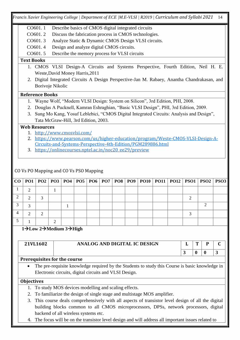
CO Vs PO Mapping and CO Vs PSO Mapping
1Low 2Medium 3High
21VL1602 ANALOG AND DIGITAL IC DESIGN L T P C
3 0 0 3
Prerequisites for the course
The pre-requisite knowledge required by the Students to study this Course is basic knowledge in
Electronic circuits, digital circuits and VLSI Design.
Objectives
1. To study MOS devices modelling and scaling effects.
2. To familiarize the design of single stage and multistage MOS amplifier.
3. This course deals comprehensively with all aspects of transistor level design of all the digital
building blocks common to all CMOS microprocessors, DPSs, network processors, digital
backend of all wireless systems etc.
4. The focus will be on the transistor level design and will address all important issues related to
CO PO1 PO2 PO3 PO4 PO5 PO6 PO7 PO8 PO9 PO10 PO11 PO12 PSO1 PSO2 PSO3
1 2 1
2 2 3 2
3 3 1 2
4 2 2 3
5 1 2
Francis Xavier Engineering College | Department of ECE |M.E-VLSI | R2019 | Curriculum and Syllabi 2021 15
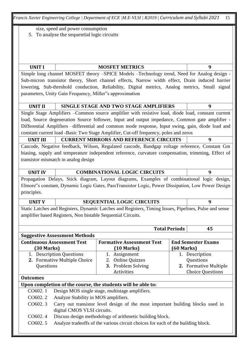
size, speed and power consumption 5. To analyse the sequential logic circuits
UNIT I MOSFET METRICS 9
Simple long channel MOSFET theory –SPICE Models –Technology trend, Need for Analog design -
Sub-micron transistor theory, Short channel effects, Narrow width effect, Drain induced barrier
lowering, Sub-threshold conduction, Reliability, Digital metrics, Analog metrics, Small signal
parameters, Unity Gain Frequency, Miller‟s approximation
UNIT II SINGLE STAGE AND TWO STAGE AMPLIFIERS 9
Single Stage Amplifiers –Common source amplifier with resistive load, diode load, constant current
load, Source degeneration Source follower, Input and output impedance, Common gate amplifier -
Differential Amplifiers –differential and common mode response, Input swing, gain, diode load and
constant current load -Basic Two Stage Amplifier, Cut-off frequency, poles and zeros
UNIT III CURRENT MIRRORS AND REFERENCE CIRCUITS 9
Cascode, Negative feedback, Wilson, Regulated cascode, Bandgap voltage reference, Constant Gm
biasing, supply and temperature independent reference, curvature compensation, trimming, Effect of
transistor mismatch in analog design
UNIT IV COMBINATIONAL LOGIC CIRCUITS 9
Propagation Delays, Stick diagram, Layout diagrams, Examples of combinational logic design,
Elmore‟s constant, Dynamic Logic Gates, PassTransistor Logic, Power Dissipation, Low Power Design
principles.
UNIT V SEQUENTIAL LOGIC CIRCUITS 9
Static Latches and Registers, Dynamic Latches and Registers, Timing Issues, Pipelines, Pulse and sense
amplifier based Registers, Non bistable Sequential Circuits.
Total Periods 45
Suggestive Assessment Methods
Continuous Assessment Test (30 Marks)
Formative Assessment Test (10 Marks)
End Semester Exams (60 Marks)
1. Description Questions 2. Formative Multiple Choice
Questions
1. Assignment 2. Online Quizzes 3. Problem Solving
Activities
1. Description Questions
2. Formative Multiple Choice Questions
Outcomes
Upon completion of the course, the students will be able to: CO602. 1 Design MOS single stage, multistage amplifiers.
CO602. 2 Analyze Stability in MOS amplifiers.
CO602. 3 Carry out transistor level design of the most important building blocks used in
digital CMOS VLSI circuits.
CO602. 4 Discuss design methodology of arithmetic building block.
CO602. 5 Analyze tradeoffs of the various circuit choices for each of the building block.
Francis Xavier Engineering College | Department of ECE |M.E-VLSI | R2019 | Curriculum and Syllabi 2021 16
Text Books
1. Behzad Razavi, “Design of Analog CMOS Integrated Circuits”, McGraw Hill, 2000
2. Jan Rabaey, Anantha Chandrakasan, B Nikolic, “Digital Integrated Circuits: A Design
Perspective”. Second Edition, Feb 2003, Prentice Hall of India
Reference Books
1. N.Weste, K. Eshraghian, “ Principles of CMOS VLSI Design”. Second Edition, 1993 Addision
Wesley.
2.Philip E.Allen, “CMOS Analog Circuit Design”, Oxford University Press, 2013
3.Paul R.Gray, “Analysis and Design of Analog Integrated Circuits”, Wiley Student edition, 5th edition,
2009.
4.R.Jacob Baker, “CMOS: Circuit Design, Layout , and Simulation”, Wiley Student Edition, 2009
Web Resources 1. https://nptel.ac.in/
2. https://nptel.ac.in/courses/117/106/117106030/
3. https://onlinecourses.nptel.ac.in/noc20_ee05/preview
CO Vs PO Mapping and CO Vs PSO Mapping
1Low 2Medium 3High
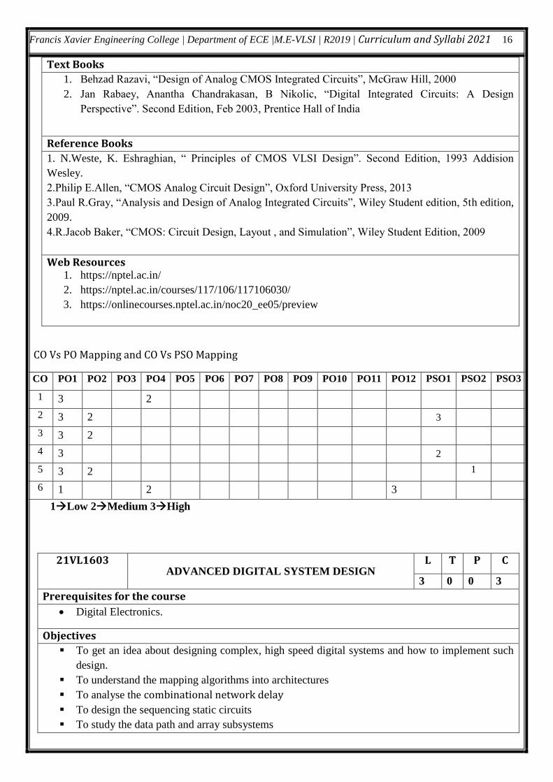
21VL1603 ADVANCED DIGITAL SYSTEM DESIGN
L T P C
3 0 0 3
Prerequisites for the course
Digital Electronics.
Objectives
To get an idea about designing complex, high speed digital systems and how to implement such
design.
To understand the mapping algorithms into architectures
To analyse the combinational network delay
To design the sequencing static circuits
To study the data path and array subsystems
CO PO1 PO2 PO3 PO4 PO5 PO6 PO7 PO8 PO9 PO10 PO11 PO12 PSO1 PSO2 PSO3
1 3 2
2 3 2 3
3 3 2
4 3 2
5 3 2 1
6 1 2 3
Francis Xavier Engineering College | Department of ECE |M.E-VLSI | R2019 | Curriculum and Syllabi 2021 17
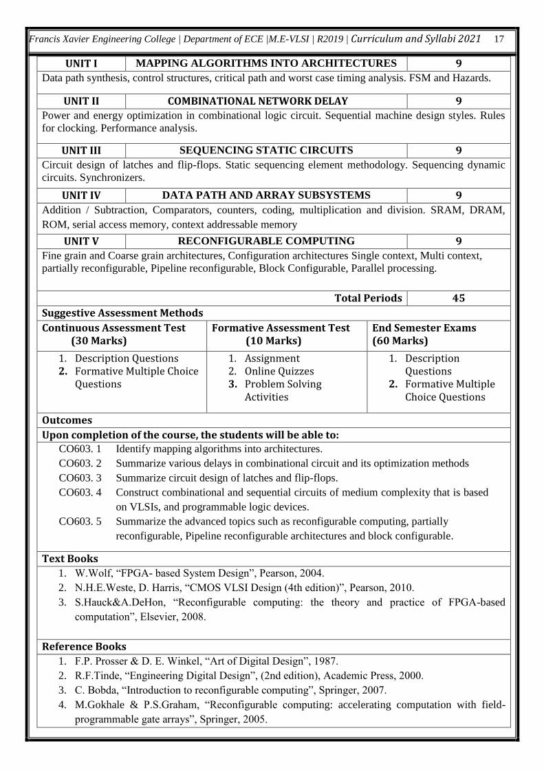
UNIT I MAPPING ALGORITHMS INTO ARCHITECTURES 9
Data path synthesis, control structures, critical path and worst case timing analysis. FSM and Hazards.
UNIT II COMBINATIONAL NETWORK DELAY 9
Power and energy optimization in combinational logic circuit. Sequential machine design styles. Rules
for clocking. Performance analysis.
UNIT III SEQUENCING STATIC CIRCUITS 9
Circuit design of latches and flip-flops. Static sequencing element methodology. Sequencing dynamic
circuits. Synchronizers.
UNIT IV DATA PATH AND ARRAY SUBSYSTEMS 9
Addition / Subtraction, Comparators, counters, coding, multiplication and division. SRAM, DRAM,
ROM, serial access memory, context addressable memory
UNIT V RECONFIGURABLE COMPUTING 9
Fine grain and Coarse grain architectures, Configuration architectures Single context, Multi context,
partially reconfigurable, Pipeline reconfigurable, Block Configurable, Parallel processing.
Total Periods 45
Suggestive Assessment Methods
Continuous Assessment Test (30 Marks)
Formative Assessment Test (10 Marks)
End Semester Exams (60 Marks)
1. Description Questions 2. Formative Multiple Choice
Questions
1. Assignment 2. Online Quizzes 3. Problem Solving
Activities
1. Description Questions
2. Formative Multiple Choice Questions
Outcomes
Upon completion of the course, the students will be able to: CO603. 1 Identify mapping algorithms into architectures.
CO603. 2 Summarize various delays in combinational circuit and its optimization methods
CO603. 3 Summarize circuit design of latches and flip-flops.
CO603. 4 Construct combinational and sequential circuits of medium complexity that is based
on VLSIs, and programmable logic devices.
CO603. 5 Summarize the advanced topics such as reconfigurable computing, partially
reconfigurable, Pipeline reconfigurable architectures and block configurable.
Text Books
1. W.Wolf, “FPGA- based System Design”, Pearson, 2004.
2. N.H.E.Weste, D. Harris, “CMOS VLSI Design (4th edition)”, Pearson, 2010.
3. S.Hauck&A.DeHon, “Reconfigurable computing: the theory and practice of FPGA-based
computation”, Elsevier, 2008.
Reference Books
1. F.P. Prosser & D. E. Winkel, “Art of Digital Design”, 1987.
2. R.F.Tinde, “Engineering Digital Design”, (2nd edition), Academic Press, 2000.
3. C. Bobda, “Introduction to reconfigurable computing”, Springer, 2007.
4. M.Gokhale & P.S.Graham, “Reconfigurable computing: accelerating computation with field-
programmable gate arrays”, Springer, 2005.
Francis Xavier Engineering College | Department of ECE |M.E-VLSI | R2019 | Curriculum and Syllabi 2021 18
5. C.Roth,” Fundamentals of Digital Logic Design”, Jaico Publishers, 5th edition., 2009.
Web Resources 1. https://www.coursera.org/learn/digital-systems
2. https://nptel.ac.in/courses/108/106/108106177/
3. https://youtu.be/M0mx8S05v60
4. https://youtu.be/vsoYlH1_hbc
5. https://www.udemy.com/course/learn-digital-system-design-module-1-from-basics/
CO Vs PO Mapping and CO Vs PSO Mapping
1Low 2Medium 3High
CO PO1 PO2 PO3 PO4 PO5 PO6 PO7 PO8 PO9 PO10 PO11 PO12 PSO1 PSO2 PSO3
1 3 3 3 3 3 2 2 1
2 3 3 3 3 3 2 2 2
3 3 3 3 3 3 2 2
4 3 3 3 3 3 2 2 2
5 3 3 3 3 2 2 2 1
21VL1911
RESEARCH METHODOLOGY FOR ENGINEERS
L T P C
3 0 0 3
Prerequisites for the course
NIL
Objectives
1. To understand some basic concepts of engineering research and its methodologies.
2. To identify various sources of information for literature review.
3. To familiarize the various procedures for analysis and optimization of research techniques
4. To understand report writing and presentation skills.
5. To understand about intellectual property rights
UNIT I INTRODUCTION TO RESEARCH METHODOLOGY 9
Research –types of research-research process, engineering research- objectives, motivation,
types,research question , formulating a research problem
UNIT II LITERATURE REVIEW 9
New and Existing Knowledge, Analysis and Synthesis, Types of Publications, Bibliographic Databases,
Measures of Research impact, keywords, Types of Plagiarism, Software Used for Identifying Plagiarism
Techniques to Avoid Plagiarism , ethics in engineering research
UNIT III ANALYSIS AND OPTIMIZATION 9
Francis Xavier Engineering College | Department of ECE |M.E-VLSI | R2019 | Curriculum and Syllabi 2021 19
CO Vs PO Mapping and CO Vs PSO Mapping
Research tools, Statistics-one dimensional, two dimensional, multidimensional, Optimization Methods –
Two parameter, multi parameter, cost function. Survey research methods
UNIT IV TECHNICALWRITING /PRESENTATION 9
Technical writing – attributes and reasons, writing strategies, Journal Paper: Structure and Approach,
Language Skills, Writing Style, and Editing, Rules of Mathematical Writing, Attributions and Citations,
Acknowledgments, patents.
UNIT V INTELLECTUAL PROPERTY RIGHTS 9
Introduction, Significance, Requirements for Patentability, Application Preparation and Filing, Forms of
IPR, IPR and Licensing, patent – examples
Total Periods 45
Suggestive Assessment Methods
Continuous Assessment Test (30 Marks)
Formative Assessment Test (10 Marks)
End Semester Exams (60 Marks)
1.Description Questions 2.Formative Multiple choice questions
1.Assignment 2.Online Quizzes 3.Problem solving Activities
1.Description Questions 2.Formative Multiple choice questions
Outcomes
Upon completion of the course, the students will be able to: CO911. 1 Demonstrate the concepts of engineering research and its methodologies.
CO911. 2 Understand the various methods used to collect the data for research.
CO911. 3 Formulate appropriate research problem and conduct the experiments using analysis
and optimization
CO911. 4 Write quality research in engineering.
CO911. 5 Understand the concepts of intellectual property rights.
Text Books
1. Dipankar Deb, Rajeeb Dey, Valentina E. Balas.”Engineering Research Methodology A
Practical Insight for Researchers”,Springer.2019
2. David V. Thiel, “Research Methods for Engineers”,cambridge university press,2014
3. Vinayak Bairagi Mousami V. Munot ,”Research Methodology A Practical And Scientific
Approach”, CRC Press, 2019
Reference Books
1. RanjitKumar, “Research Methodology a step-by-step guide for beginners” SAGE publications,
Fifth edition,2019
Web Resources https://nptel.ac.in/courses/107/108/107108011/ https://onlinecourses.swayam2.ac.in/cec20_hs17/preview
CO PO1 PO2 PO3 PO4 PO5 PO6 PO7 PO8 PO9 PO10 PO11 PO12 PSO1 PSO2 PSO3
1 3 3 1 3 3 2 1 1
2 3 3 1 3 3 2 1 1
Francis Xavier Engineering College | Department of ECE |M.E-VLSI | R2019 | Curriculum and Syllabi 2021 20
1Low 2Medium 3High
21VL1611 Advanced Digital System Design Laboratory L T P C
0 0 4 2
Prerequisites for the course
Digital Electronics, VLSI Design Objectives
1. To understand complex combinational circuits using HDL at behavioral, structural and
RTL levels.
2. To understand complex sequential circuits using HDL at behavioral, structural and RTL levels.
3. To write the test benches to simulate combinational and sequential circuits.
4. To Learn how the language infers hardware and helps to simulate and synthesize the digital system
5. To the digital systems using FPGAs with respect to speed and area. S.No List of Experiments CO
Using Verilog code design, simulate and synthesize the following with a suitable FPGA.
1. 8 to 3 programmable priority encoders. CO1
2. Full Adder using structural modeling CO1
3. Flip Flops (D, SR, T, JK) CO2
4. 3-bit arbitrary Counter, 4 bit binary up/down/up-down counter with
synchronous reset, 4 bit Johnson counter, BCD counter CO2
5. Sequential block to detect a sequence (say 11101) using appropriate CO2
6. FSM 8-bit ripple carry adder and carry skip adder CO3
7. 8-bit Carry Select Adder CO3
8. 8-bit Serial, Parallel Multiplier and generate report on area and
delay
CO3
9. Develop the behavioural style HDL code for 4-bit counter.Develop
the structural style HDLcode for 4-bit counter using T Flip Flop (use
of generate statement, area-performanceanalysis after synthesize).
Compile, synthesize and simulate each design entity and verify the
functionality by creatingvector waveform file.
CO4
Using System Verilog code, simulate the following
10. Full Subtractor using structural modeling CO4
11. Flip Flops (D, SR, T, JK) CO5
12. Design NAND and NOR standard cells, draw the layout for D
andSR latch. Do DRC, LVS and Extraction. CO5
Total Periods :60
3 3 3 1 3 3 2 1 1
4 3 3 1 3 3 2 1 1
5 3 3 1 3 3 2 1 1
Francis Xavier Engineering College | Department of ECE |M.E-VLSI | R2019 | Curriculum and Syllabi 2021 21
Suggestive Assessment Methods
Lab Components Assessments
(50 Marks)
End Semester Exams
(50 Marks)
1.Experiment
2.Model lab exam 1.End semester lab exam
Outcomes
Upon completion of the course, the students will be able to:
Laboratory Requirements
CO611.1. Design and model complex combinational circuits using HDL at behavioral, structural and
RTL levels.
CO611.2. Design and model complex sequential circuits using HDL at behavioral, structural and RTL
levels.
CO611.3. Develop the test benches to simulate combinational and sequential circuits.
CO611.4. Learn how the language infers hardware and helps to simulate and synthesize the digital
system.
CO611.5. Implement and analyze the digital systems using FPGAs with respect to speed and area.
Reference Books
1. Peter J. Ashenden, “Digital Design: An Embedded Systems Approach using Verilog”, Elsevier, 2010.
2. Samir Palnitkar, “Verilog HDL: A Guide to Digital Design and Synthesis”, Pearson Education, 2nd
Edition, 2010.
3. Stuart Sutherland, “RTL Modeling with System Verilog for Simulation and Synthesis:
Using System Verilog for ASIC and FPGA Design”, Create Space Independent Publishing
Platform, First Edition, 2017.
Web Resources
1. https://nptel.ac.in/courses/117/105/117105080/ 2. https://www.xilinx.com/support/documentation/sw_manuals/xilinx2020_2/ug888-vivado-
design-flows-overview-tutorial.pdf 3. https://www.xilinx.com/support/documentation/university/Vivado-Teaching/HDL-
Design/2015x/VHDL/docs-pdf/Vivado_Tutorial.pdf
CO Vs PO Mapping and CO Vs PSO Mapping
CO PO
1
PO
2
PO
3
PO
4
PO
5
PO
6
PO
7
PO
8
PO
9
PO1
0
PO1
1
PO1
2
PSO
1
PSO
2
PSO
3
1 1 2 2
2 2 2 3
3 2 1
4 1 2 1 2
5 2 1
Francis Xavier Engineering College | Department of ECE |M.E-VLSI | R2019 | Curriculum and Syllabi 2021 22
SEMESTER II
S.No. Course Code
Course Category Contact Periods
L T P C
Theory Courses
1 21VL2601 Low Power VLSI Design PC 3 3 0 0 3
2 Professional Elective III PE 3 3 0 0 3
3 Professional Elective IV PE 3 3 0 0 3
4 Professional Elective V PE 3 3 0 0 3
5 Professional Elective VI PE 3 3 0 0 3
Theory cum Practical Courses
1 21VL2602 IC Design for Communications PC 5 3 0 2 4
Practical Courses
1 21VL2611
Analog and Digital IC Design
Laboratory PC 4 0 0 4 2
2 21VL2911
Advanced Design and Analysis
Laboratory EEC 4 0 0 4 2
Total 28 18 0 10 23
21VL2601 LOW POWER VLSI DESIGN L T P C
3 0 0 3
Prerequisites for the course
CMOS VLSI Design
Objectives
1. Identify sources of power in an IC.
2. To identify the power dissipation mechanisms in various MOS logic styles
3. To familiarize suitable techniques to reduce power dissipation
4. To know the design concepts of micro sensors and micro actuators.
5. To familiarize concepts of quantum mechanics and nano systems.
UNIT I POWER DISSIPATION IN CMOS 9
Physics of power dissipation in CMOS FET devices – Sources of power consumption – Static Power
Dissipation, Active Power Dissipation - Basic principle of low power design, Need for low power VLSI
chips, Sources of power dissipation on Digital Integrated circuits, Emerging Low power approaches.
UNIT II POWER OPTIMIZATION 9
Logic level power optimization – Circuit level low power design – Standard Adder Cells, CMOS Adders
Architectures-BiCMOS adders - Low Voltage Low Power Design Techniques, Current Mode Adders -
Types Of Multiplier Architectures, Braun, Booth and Wallace Tree Multipliers and their performance
comparison
Francis Xavier Engineering College | Department of ECE |M.E-VLSI | R2019 | Curriculum and Syllabi 2021 23
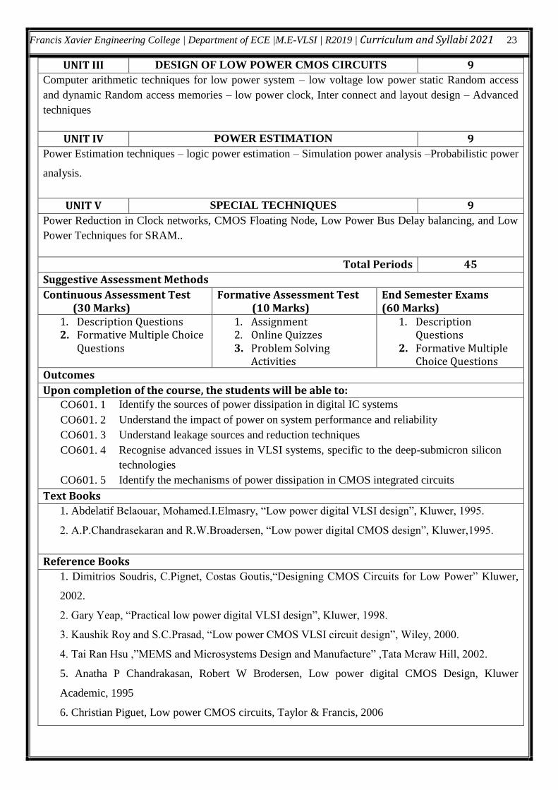
UNIT III DESIGN OF LOW POWER CMOS CIRCUITS 9
Computer arithmetic techniques for low power system – low voltage low power static Random access
and dynamic Random access memories – low power clock, Inter connect and layout design – Advanced
techniques
UNIT IV POWER ESTIMATION 9
Power Estimation techniques – logic power estimation – Simulation power analysis –Probabilistic power
analysis.
UNIT V SPECIAL TECHNIQUES 9
Power Reduction in Clock networks, CMOS Floating Node, Low Power Bus Delay balancing, and Low
Power Techniques for SRAM..
Total Periods 45
Suggestive Assessment Methods
Continuous Assessment Test (30 Marks)
Formative Assessment Test (10 Marks)
End Semester Exams (60 Marks)
1. Description Questions 2. Formative Multiple Choice
Questions
1. Assignment 2. Online Quizzes 3. Problem Solving
Activities
1. Description Questions
2. Formative Multiple Choice Questions
Outcomes
Upon completion of the course, the students will be able to:
CO601. 1 Identify the sources of power dissipation in digital IC systems
CO601. 2 Understand the impact of power on system performance and reliability
CO601. 3 Understand leakage sources and reduction techniques
CO601. 4 Recognise advanced issues in VLSI systems, specific to the deep-submicron silicon
technologies
CO601. 5 Identify the mechanisms of power dissipation in CMOS integrated circuits
Text Books
1. Abdelatif Belaouar, Mohamed.I.Elmasry, “Low power digital VLSI design”, Kluwer, 1995.
2. A.P.Chandrasekaran and R.W.Broadersen, “Low power digital CMOS design”, Kluwer,1995.
Reference Books
1. Dimitrios Soudris, C.Pignet, Costas Goutis,“Designing CMOS Circuits for Low Power” Kluwer,
2002.
2. Gary Yeap, “Practical low power digital VLSI design”, Kluwer, 1998.
3. Kaushik Roy and S.C.Prasad, “Low power CMOS VLSI circuit design”, Wiley, 2000.
4. Tai Ran Hsu ,”MEMS and Microsystems Design and Manufacture” ,Tata Mcraw Hill, 2002.
5. Anatha P Chandrakasan, Robert W Brodersen, Low power digital CMOS Design, Kluwer
Academic, 1995
6. Christian Piguet, Low power CMOS circuits, Taylor & Francis, 2006
Francis Xavier Engineering College | Department of ECE |M.E-VLSI | R2019 | Curriculum and Syllabi 2021 24
Web Resources 1. https://www.youtube.com/watch?v=TFOO1JAll2Y
2. https://www.intechopen.com/books/very-large-scale-integration/low-power-
design-methodology
3. https://nptel.ac.in/courses/106/105/106105034/
CO Vs PO Mapping and CO Vs PSO Mapping
1Low 2Medium 3High
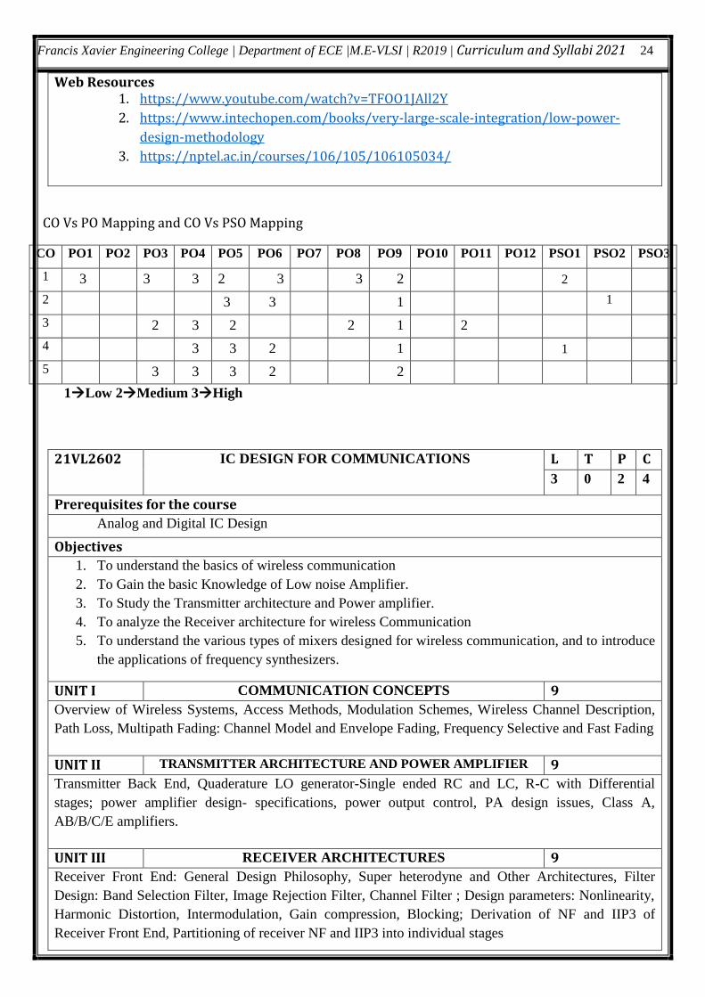
21VL2602 IC DESIGN FOR COMMUNICATIONS
L T P C
3 0 2 4
Prerequisites for the course
Analog and Digital IC Design
Objectives
1. To understand the basics of wireless communication
2. To Gain the basic Knowledge of Low noise Amplifier.
3. To Study the Transmitter architecture and Power amplifier.
4. To analyze the Receiver architecture for wireless Communication
5. To understand the various types of mixers designed for wireless communication, and to introduce
the applications of frequency synthesizers.
UNIT I COMMUNICATION CONCEPTS 9
Overview of Wireless Systems, Access Methods, Modulation Schemes, Wireless Channel Description,
Path Loss, Multipath Fading: Channel Model and Envelope Fading, Frequency Selective and Fast Fading
UNIT II TRANSMITTER ARCHITECTURE AND POWER AMPLIFIER 9
Transmitter Back End, Quaderature LO generator-Single ended RC and LC, R-C with Differential
stages; power amplifier design- specifications, power output control, PA design issues, Class A,
AB/B/C/E amplifiers.
UNIT III RECEIVER ARCHITECTURES 9
Receiver Front End: General Design Philosophy, Super heterodyne and Other Architectures, Filter
Design: Band Selection Filter, Image Rejection Filter, Channel Filter ; Design parameters: Nonlinearity,
Harmonic Distortion, Intermodulation, Gain compression, Blocking; Derivation of NF and IIP3 of
Receiver Front End, Partitioning of receiver NF and IIP3 into individual stages
CO PO1 PO2 PO3 PO4 PO5 PO6 PO7 PO8 PO9 PO10 PO11 PO12 PSO1 PSO2 PSO3
1 3 3 3 2 3 3 2 2
2 3 3 1 1
3 2 3 2 2 1 2
4 3 3 2 1 1
5 3 3 3 2 2
Francis Xavier Engineering College | Department of ECE |M.E-VLSI | R2019 | Curriculum and Syllabi 2021 25
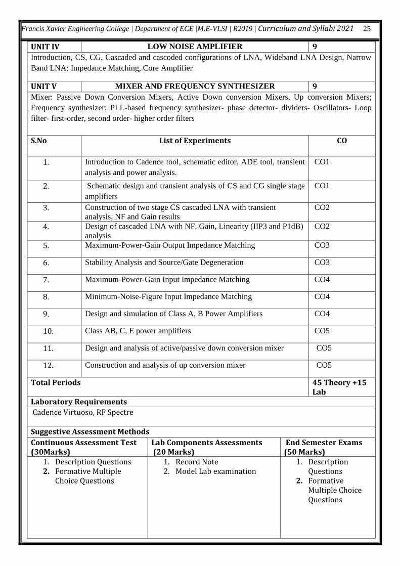
UNIT IV LOW NOISE AMPLIFIER 9
Introduction, CS, CG, Cascaded and cascoded configurations of LNA, Wideband LNA Design, Narrow
Band LNA: Impedance Matching, Core Amplifier
UNIT V MIXER AND FREQUENCY SYNTHESIZER 9
Mixer: Passive Down Conversion Mixers, Active Down conversion Mixers, Up conversion Mixers;
Frequency synthesizer: PLL-based frequency synthesizer- phase detector- dividers- Oscillators- Loop
filter- first-order, second order- higher order filters
S.No List of Experiments CO
1. Introduction to Cadence tool, schematic editor, ADE tool, transient
analysis and power analysis.
CO1
2. Schematic design and transient analysis of CS and CG single stage
amplifiers
CO1
3. Construction of two stage CS cascaded LNA with transient
analysis, NF and Gain results
CO2
4. Design of cascaded LNA with NF, Gain, Linearity (IIP3 and P1dB)
analysis
CO2
5. Maximum-Power-Gain Output Impedance Matching CO3
6. Stability Analysis and Source/Gate Degeneration CO3
7. Maximum-Power-Gain Input Impedance Matching CO4
8. Minimum-Noise-Figure Input Impedance Matching CO4
9. Design and simulation of Class A, B Power Amplifiers CO4
10. Class AB, C, E power amplifiers CO5
11. Design and analysis of active/passive down conversion mixer CO5
12. Construction and analysis of up conversion mixer CO5
Total Periods 45 Theory +15 Lab
Laboratory Requirements
Cadence Virtuoso, RF Spectre
Suggestive Assessment Methods
Continuous Assessment Test (30Marks)
Lab Components Assessments (20 Marks)
End Semester Exams (50 Marks)
1. Description Questions 2. Formative Multiple
Choice Questions
1. Record Note 2. Model Lab examination
1. Description Questions
2. Formative Multiple Choice Questions
Francis Xavier Engineering College | Department of ECE |M.E-VLSI | R2019 | Curriculum and Syllabi 2021 26
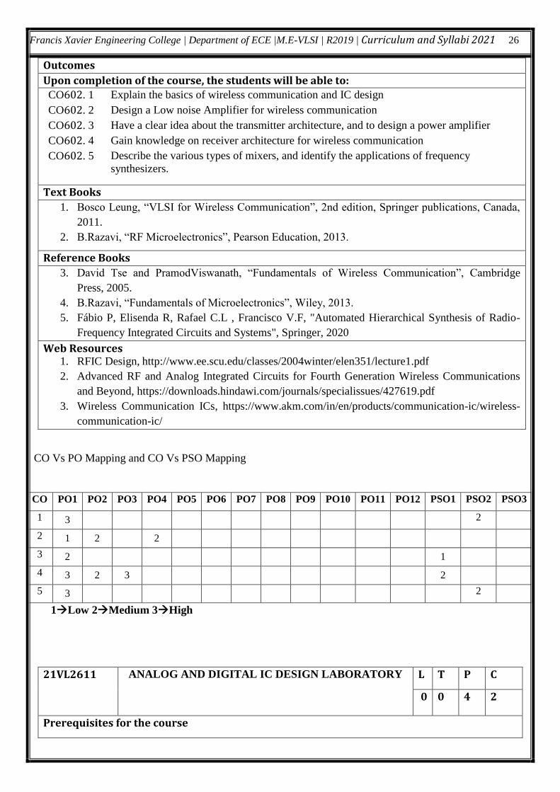
Outcomes
Upon completion of the course, the students will be able to:
CO602. 1 Explain the basics of wireless communication and IC design
CO602. 2 Design a Low noise Amplifier for wireless communication
CO602. 3 Have a clear idea about the transmitter architecture, and to design a power amplifier
CO602. 4 Gain knowledge on receiver architecture for wireless communication
CO602. 5 Describe the various types of mixers, and identify the applications of frequency
synthesizers.
Text Books
1. Bosco Leung, “VLSI for Wireless Communication”, 2nd edition, Springer publications, Canada,
2011.
2. B.Razavi, “RF Microelectronics”, Pearson Education, 2013.
Reference Books
3. David Tse and PramodViswanath, “Fundamentals of Wireless Communication”, Cambridge
Press, 2005.
4. B.Razavi, “Fundamentals of Microelectronics”, Wiley, 2013.
5. Fábio P, Elisenda R, Rafael C.L , Francisco V.F, "Automated Hierarchical Synthesis of Radio-
Frequency Integrated Circuits and Systems", Springer, 2020
Web Resources 1. RFIC Design, http://www.ee.scu.edu/classes/2004winter/elen351/lecture1.pdf
2. Advanced RF and Analog Integrated Circuits for Fourth Generation Wireless Communications
and Beyond, https://downloads.hindawi.com/journals/specialissues/427619.pdf
3. Wireless Communication ICs, https://www.akm.com/in/en/products/communication-ic/wireless-
communication-ic/
CO Vs PO Mapping and CO Vs PSO Mapping
1Low 2Medium 3High
21VL2611 ANALOG AND DIGITAL IC DESIGN LABORATORY
L T P C
0 0 4 2
Prerequisites for the course
CO PO1 PO2 PO3 PO4 PO5 PO6 PO7 PO8 PO9 PO10 PO11 PO12 PSO1 PSO2 PSO3
1 3 2
2 1 2 2
3 2 1
4 3 2 3 2
5 3 2
Francis Xavier Engineering College | Department of ECE |M.E-VLSI | R2019 | Curriculum and Syllabi 2021 27
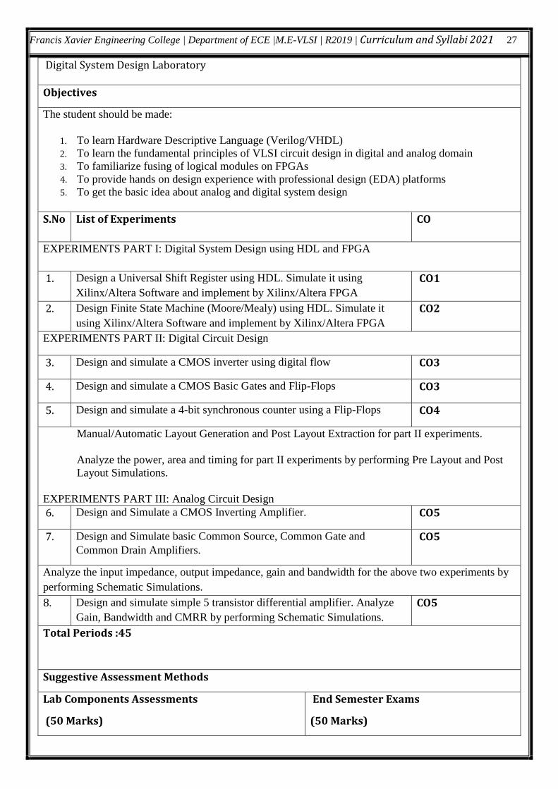
Digital System Design Laboratory
Objectives
The student should be made:
1. To learn Hardware Descriptive Language (Verilog/VHDL)
2. To learn the fundamental principles of VLSI circuit design in digital and analog domain
3. To familiarize fusing of logical modules on FPGAs
4. To provide hands on design experience with professional design (EDA) platforms 5. To get the basic idea about analog and digital system design
S.No List of Experiments CO
EXPERIMENTS PART I: Digital System Design using HDL and FPGA
1. Design a Universal Shift Register using HDL. Simulate it using
Xilinx/Altera Software and implement by Xilinx/Altera FPGA
CO1
2. Design Finite State Machine (Moore/Mealy) using HDL. Simulate it
using Xilinx/Altera Software and implement by Xilinx/Altera FPGA
CO2
EXPERIMENTS PART II: Digital Circuit Design
3. Design and simulate a CMOS inverter using digital flow CO3
4. Design and simulate a CMOS Basic Gates and Flip-Flops CO3
5. Design and simulate a 4-bit synchronous counter using a Flip-Flops CO4
Manual/Automatic Layout Generation and Post Layout Extraction for part II experiments.
Analyze the power, area and timing for part II experiments by performing Pre Layout and Post
Layout Simulations.
EXPERIMENTS PART III: Analog Circuit Design 6. Design and Simulate a CMOS Inverting Amplifier. CO5
7. Design and Simulate basic Common Source, Common Gate and
Common Drain Amplifiers. CO5
Analyze the input impedance, output impedance, gain and bandwidth for the above two experiments by
performing Schematic Simulations.
8. Design and simulate simple 5 transistor differential amplifier. Analyze
Gain, Bandwidth and CMRR by performing Schematic Simulations.
CO5
Total Periods :45
Suggestive Assessment Methods
Lab Components Assessments
(50 Marks)
End Semester Exams
(50 Marks)
Francis Xavier Engineering College | Department of ECE |M.E-VLSI | R2019 | Curriculum and Syllabi 2021 28
1.Experiment
2.Model lab exam 1.End semester lab exam
Outcomes
At the end of the course, the student should be able to:
CO611.1. Write HDL code for basic as well as advanced digital integrated circuit
CO611.2. Import the logic modules into FPGA Boards
CO611.3. Synthesize Place and Route the digital IPs
CO611.4. Design the layouts of Digital and Analog IC Blocks using EDA tools
CO611.5. Simulate the layouts of Digital and Analog IC Blocks using EDA tools
Laboratory Requirements
1. Xilinx ISE/Altera Quartus/ equivalent EDA Tools 10 User License
2. Xilinx/Altera/equivalent FPGA Boards 10 no
3. Cadence/Synopsis/ Mentor Graphics/Tanner/equivalent EDA Tools 10 User License
4. Personal Computer 20 no
Reference Books
1.Neil H. E. Weste , David Money Harris -CMOS VLSI Design-A Circuits and Systems Perspective,
Fourth Edition,2011
2. Design Verification with E. by Samir Palnitkar, Prentice Hall , 2003
Web Resources
1. https://resources.pcb.cadence.com/blog/2019-working-with-analog-vs-digital-integrated-
circuits-in-your-layout
2. https://www.cadence.com/ko_KR/home/tools/custom-ic-analog-rf-design/custom-ic-
analog-rf-flows.html
3. https://web.itu.edu.tr/~ateserd/CADENCE%20Manual.pdf
CO Vs PO Mapping and CO Vs PSO Mapping
1Low 2Medium 3High
21VL2911 Advanced Design and Analysis Laboratory L T P C
0 0 4 2
CO PO
1
PO
2
PO
3
PO
4
PO
5
PO
6
PO
7
PO
8
PO
9
PO1
0
PO1
1
PO1
2
PSO
1
PSO
2
PSO
3
1 3 3 1
2 2 2 2 2
3 2 3 3
4 1 2 2
5 2 2 1
Francis Xavier Engineering College | Department of ECE |M.E-VLSI | R2019 | Curriculum and Syllabi 2021 29
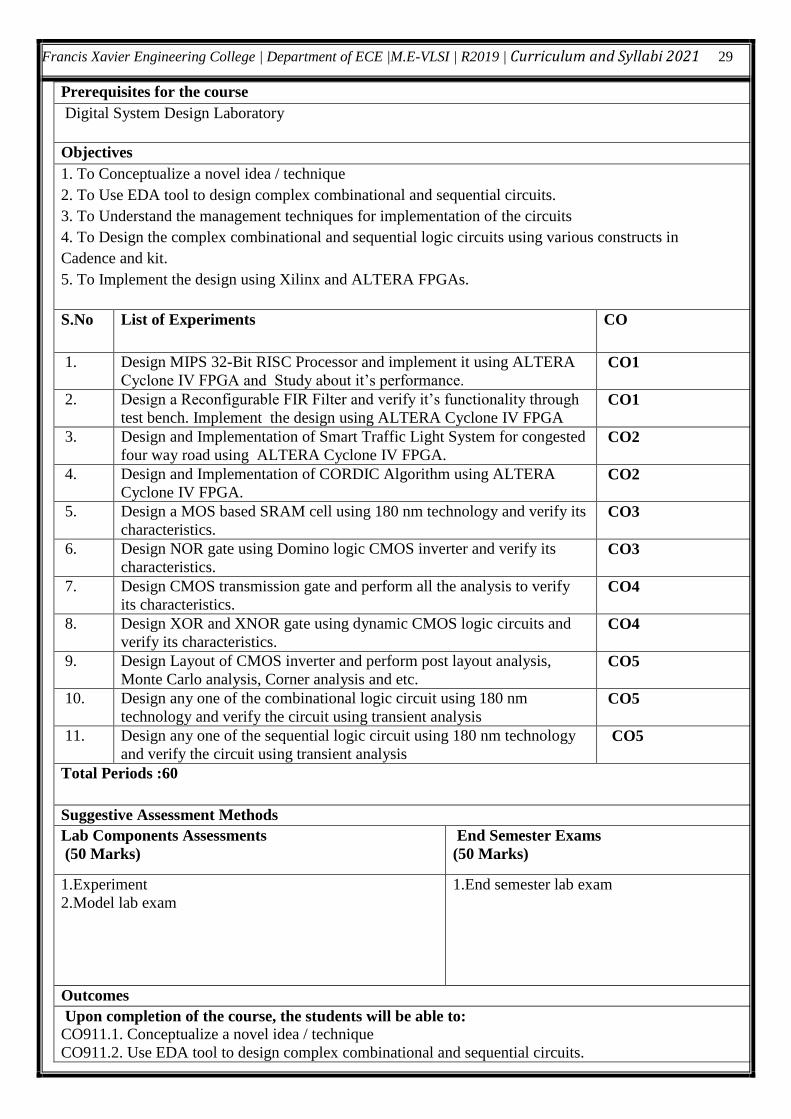
Prerequisites for the course
Digital System Design Laboratory
Objectives
1. To Conceptualize a novel idea / technique
2. To Use EDA tool to design complex combinational and sequential circuits.
3. To Understand the management techniques for implementation of the circuits
4. To Design the complex combinational and sequential logic circuits using various constructs in
Cadence and kit.
5. To Implement the design using Xilinx and ALTERA FPGAs.
S.No List of Experiments CO
1. Design MIPS 32-Bit RISC Processor and implement it using ALTERA
Cyclone IV FPGA and Study about it’s performance. CO1
2. Design a Reconfigurable FIR Filter and verify it’s functionality through
test bench. Implement the design using ALTERA Cyclone IV FPGA CO1
3. Design and Implementation of Smart Traffic Light System for congested
four way road using ALTERA Cyclone IV FPGA. CO2
4. Design and Implementation of CORDIC Algorithm using ALTERA
Cyclone IV FPGA. CO2
5. Design a MOS based SRAM cell using 180 nm technology and verify its
characteristics. CO3
6. Design NOR gate using Domino logic CMOS inverter and verify its
characteristics. CO3
7. Design CMOS transmission gate and perform all the analysis to verify
its characteristics. CO4
8. Design XOR and XNOR gate using dynamic CMOS logic circuits and
verify its characteristics. CO4
9. Design Layout of CMOS inverter and perform post layout analysis,
Monte Carlo analysis, Corner analysis and etc. CO5
10. Design any one of the combinational logic circuit using 180 nm
technology and verify the circuit using transient analysis CO5
11. Design any one of the sequential logic circuit using 180 nm technology
and verify the circuit using transient analysis CO5
Total Periods :60
Suggestive Assessment Methods
Lab Components Assessments
(50 Marks)
End Semester Exams
(50 Marks)
1.Experiment
2.Model lab exam
1.End semester lab exam
Outcomes
Upon completion of the course, the students will be able to:
CO911.1. Conceptualize a novel idea / technique
CO911.2. Use EDA tool to design complex combinational and sequential circuits.
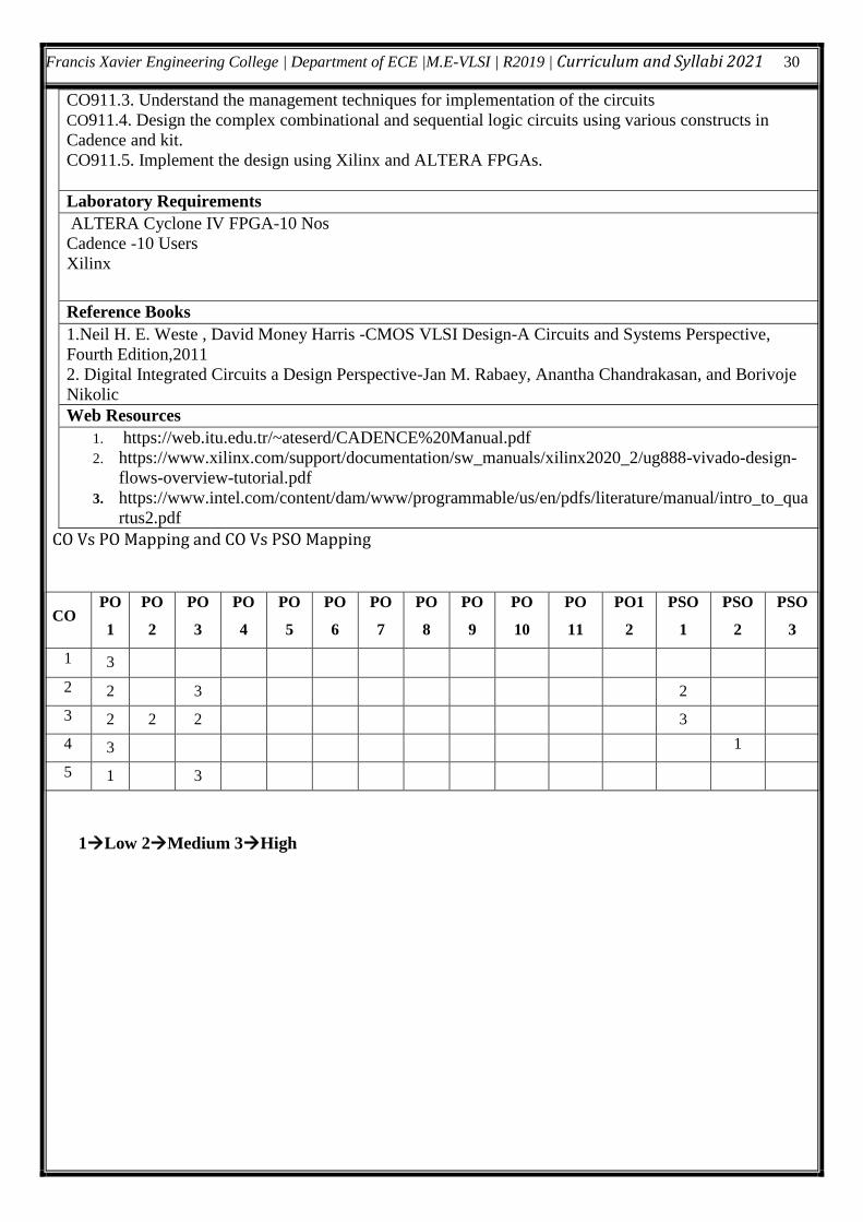
Francis Xavier Engineering College | Department of ECE |M.E-VLSI | R2019 | Curriculum and Syllabi 2021 30
CO911.3. Understand the management techniques for implementation of the circuits
CO911.4. Design the complex combinational and sequential logic circuits using various constructs in
Cadence and kit.
CO911.5. Implement the design using Xilinx and ALTERA FPGAs.
Laboratory Requirements
ALTERA Cyclone IV FPGA-10 Nos
Cadence -10 Users
Xilinx
Reference Books
1.Neil H. E. Weste , David Money Harris -CMOS VLSI Design-A Circuits and Systems Perspective,
Fourth Edition,2011
2. Digital Integrated Circuits a Design Perspective-Jan M. Rabaey, Anantha Chandrakasan, and Borivoje
Nikolic
Web Resources
1. https://web.itu.edu.tr/~ateserd/CADENCE%20Manual.pdf
2. https://www.xilinx.com/support/documentation/sw_manuals/xilinx2020_2/ug888-vivado-design-
flows-overview-tutorial.pdf
3. https://www.intel.com/content/dam/www/programmable/us/en/pdfs/literature/manual/intro_to_qua
rtus2.pdf
CO Vs PO Mapping and CO Vs PSO Mapping
1Low 2Medium 3High
CO PO
1
PO
2
PO
3
PO
4
PO
5
PO
6
PO
7
PO
8
PO
9
PO
10
PO
11
PO1
2
PSO
1
PSO
2
PSO
3
1 3
2 2 3 2
3 2 2 2 3
4 3 1
5 1 3
Francis Xavier Engineering College | Department of ECE |M.E-VLSI | R2019 | Curriculum and Syllabi 2021 31
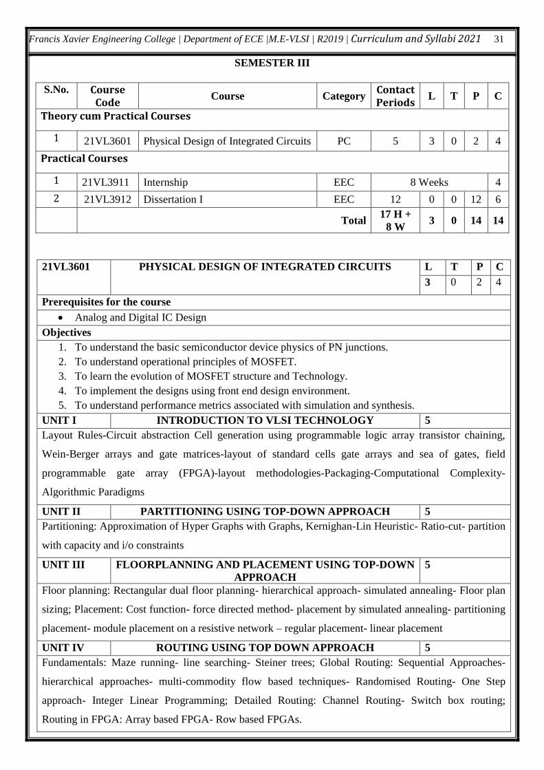
SEMESTER III
S.No. Course Code
Course Category Contact Periods
L T P C
Theory cum Practical Courses
1 21VL3601 Physical Design of Integrated Circuits PC 5 3 0 2 4
Practical Courses
1 21VL3911 Internship EEC 8 Weeks 4
2 21VL3912 Dissertation I EEC 12 0 0 12 6
Total
17 H +
8 W 3 0 14 14
21VL3601 PHYSICAL DESIGN OF INTEGRATED CIRCUITS L T P C
3 0 2 4
Prerequisites for the course
Analog and Digital IC Design
Objectives
1. To understand the basic semiconductor device physics of PN junctions.
2. To understand operational principles of MOSFET.
3. To learn the evolution of MOSFET structure and Technology.
4. To implement the designs using front end design environment.
5. To understand performance metrics associated with simulation and synthesis.
UNIT I INTRODUCTION TO VLSI TECHNOLOGY 5
Layout Rules-Circuit abstraction Cell generation using programmable logic array transistor chaining,
Wein-Berger arrays and gate matrices-layout of standard cells gate arrays and sea of gates, field
programmable gate array (FPGA)-layout methodologies-Packaging-Computational Complexity-
Algorithmic Paradigms
UNIT II PARTITIONING USING TOP-DOWN APPROACH 5
Partitioning: Approximation of Hyper Graphs with Graphs, Kernighan-Lin Heuristic- Ratio-cut- partition
with capacity and i/o constraints
UNIT III FLOORPLANNING AND PLACEMENT USING TOP-DOWN
APPROACH
5
Floor planning: Rectangular dual floor planning- hierarchical approach- simulated annealing- Floor plan
sizing; Placement: Cost function- force directed method- placement by simulated annealing- partitioning
placement- module placement on a resistive network – regular placement- linear placement
UNIT IV ROUTING USING TOP DOWN APPROACH 5
Fundamentals: Maze running- line searching- Steiner trees; Global Routing: Sequential Approaches-
hierarchical approaches- multi-commodity flow based techniques- Randomised Routing- One Step
approach- Integer Linear Programming; Detailed Routing: Channel Routing- Switch box routing;
Routing in FPGA: Array based FPGA- Row based FPGAs.
Francis Xavier Engineering College | Department of ECE |M.E-VLSI | R2019 | Curriculum and Syllabi 2021 32
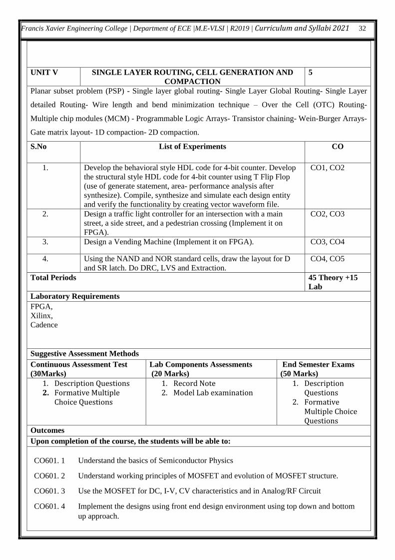
UNIT V SINGLE LAYER ROUTING, CELL GENERATION AND
COMPACTION
5
Planar subset problem (PSP) - Single layer global routing- Single Layer Global Routing- Single Layer
detailed Routing- Wire length and bend minimization technique – Over the Cell (OTC) Routing-
Multiple chip modules (MCM) - Programmable Logic Arrays- Transistor chaining- Wein-Burger Arrays-
Gate matrix layout- 1D compaction- 2D compaction.
S.No List of Experiments CO
1. Develop the behavioral style HDL code for 4-bit counter. Develop
the structural style HDL code for 4-bit counter using T Flip Flop
(use of generate statement, area- performance analysis after
synthesize). Compile, synthesize and simulate each design entity
and verify the functionality by creating vector waveform file.
CO1, CO2
2. Design a traffic light controller for an intersection with a main
street, a side street, and a pedestrian crossing (Implement it on
FPGA).
CO2, CO3
3. Design a Vending Machine (Implement it on FPGA). CO3, CO4
4. Using the NAND and NOR standard cells, draw the layout for D
and SR latch. Do DRC, LVS and Extraction.
CO4, CO5
Total Periods 45 Theory +15
Lab
Laboratory Requirements
FPGA,
Xilinx,
Cadence
Suggestive Assessment Methods
Continuous Assessment Test
(30Marks)
Lab Components Assessments
(20 Marks)
End Semester Exams
(50 Marks)
1. Description Questions 2. Formative Multiple
Choice Questions
1. Record Note 2. Model Lab examination
1. Description Questions
2. Formative Multiple Choice Questions
Outcomes
Upon completion of the course, the students will be able to:
CO601. 1 Understand the basics of Semiconductor Physics
CO601. 2 Understand working principles of MOSFET and evolution of MOSFET structure.
CO601. 3 Use the MOSFET for DC, I-V, CV characteristics and in Analog/RF Circuit
CO601. 4 Implement the designs using front end design environment using top down and bottom
up approach.
Francis Xavier Engineering College | Department of ECE |M.E-VLSI | R2019 | Curriculum and Syllabi 2021 33
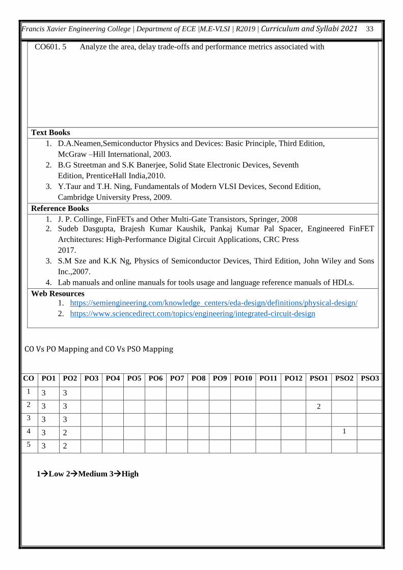
CO601. 5 Analyze the area, delay trade-offs and performance metrics associated with
Text Books
1. D.A.Neamen,Semiconductor Physics and Devices: Basic Principle, Third Edition,
McGraw –Hill International, 2003.
2. B.G Streetman and S.K Banerjee, Solid State Electronic Devices, Seventh
Edition, PrenticeHall India,2010.
3. Y.Taur and T.H. Ning, Fundamentals of Modern VLSI Devices, Second Edition,
Cambridge University Press, 2009.
Reference Books
1. J. P. Collinge, FinFETs and Other Multi-Gate Transistors, Springer, 2008
2. Sudeb Dasgupta, Brajesh Kumar Kaushik, Pankaj Kumar Pal Spacer, Engineered FinFET
Architectures: High-Performance Digital Circuit Applications, CRC Press
2017.
3. S.M Sze and K.K Ng, Physics of Semiconductor Devices, Third Edition, John Wiley and Sons
Inc.,2007.
4. Lab manuals and online manuals for tools usage and language reference manuals of HDLs.
Web Resources
1. https://semiengineering.com/knowledge_centers/eda-design/definitions/physical-design/
2. https://www.sciencedirect.com/topics/engineering/integrated-circuit-design
CO Vs PO Mapping and CO Vs PSO Mapping
1Low 2Medium 3High
CO PO1 PO2 PO3 PO4 PO5 PO6 PO7 PO8 PO9 PO10 PO11 PO12 PSO1 PSO2 PSO3
1 3 3
2 3 3 2
3 3 3
4 3 2 1
5 3 2
Francis Xavier Engineering College | Department of ECE |M.E-VLSI | R2019 | Curriculum and Syllabi 2021 34
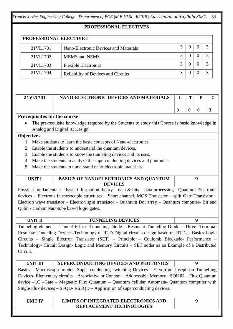
PROFESSIONAL ELECTIVES
PROFESSIONAL ELECTIVE I
21VL1701 Nano-Electronic Devices and Materials 3 0 0 3
21VL1702 MEMS and NEMS 3 0 0 3
21VL1703 Flexible Electronics 3 0 0 3
21VL1704 Reliability of Devices and Circuits 3 0 0 3
21VL1701 NANO-ELECTRONIC DEVICES AND MATERIALS L T P C
3 0 0 3
Prerequisites for the course
The pre-requisite knowledge required by the Students to study this Course is basic knowledge in
Analog and Digital IC Design.
Objectives
1. Make students to learn the basic concepts of Nano-electronics.
2. Enable the students to understand the quantum devices.
3. Enable the students to know the tunneling devices and its uses.
4. Make the students to analyze the superconducting devices and photonics.
5. Make the students to understand nano-electronic materials.
UNIT I BASICS OF NANOELECTRONICS AND QUANTUM
DEVICES 9
Physical fundamentals – basic information theory – data & bits – data processing - Quantum Electronic
devices – Electrons in mesocopic structures – Short channel, MOS Transistor – split Gate Transistor –
Electron wave transistor – Electron spin transistor – Quantum Dot array – Quantum computer- Bit and
Qubit - Carbon Nanotube based logic gates.
UNIT II TUNNELING DEVICES 9
Tunneling element – Tunnel Effect -Tunneling Diode – Resonant Tunneling Diode – Three -Terminal
Resonate Tunneling Devices-Technology of RTD-Digital circuits design based on RTDs - Basics Logic
Circuits – Single Electron Transistor (SET) – Principle – Coulomb Blockade- Performance –
Technology- Circuit Design- Logic and Memory Circuits – SET adder as an Example of a Distributed
Circuit.
UNIT III SUPERCONDUCTING DEVICES AND PHOTONICS 9
Basics - Macroscopic model- Super conducting switching Devices – Cryotron- Josephson Tunnelling
Devices- Elementary circuits – Associative or Content – Addressable Memory - SQUID – Flux Quantum
device –LC –Gate – Magnetic Flux Quantum – Quantum cellular Automata- Quantum computer with
Single Flux devices – SFQD- RSFQD – Application of superconducting devices.
UNIT IV LIMITS OF INTEGRATED ELECTRONICS AND
REPLACEMENT TECHNOLOGIES 9
Francis Xavier Engineering College | Department of ECE |M.E-VLSI | R2019 | Curriculum and Syllabi 2021 35
Survey about the limits- replacement technologies-energy supply and heat dissipation-parameter spread
as limiting effect- limits due to thermal particle motion- reliability as limiting factor-physical limits-final
objectives of integrated chips and systems.
UNIT V NANO-ELECTRONIC MATERIALS 9
Compound semiconductors - Compound semiconductors MOSFETs in the context of channel
quantization and strain, Hetero structure MOSFETs, exploiting novel materials, strain, quantization.
Emerging nano materials: CNT, Graphene, Nanotubes, nanorods and other nano-structures.
Total Periods 45
Suggestive Assessment Methods
Continuous Assessment Test (30 Marks)
Formative Assessment Test (10 Marks)
End Semester Exams (60 Marks)
1. Description Questions 2. Formative Multiple Choice
Questions
1. Assignment 2. Online Quizzes 3. Problem Solving
Activities
1. Description Questions
2. Formative Multiple Choice Questions
Outcomes
Upon completion of the course, the students will be able to:
CO701. 1 Understand basic and advanced concepts of Nano electronic devices, sensors and
transducers and their applications in Nanotechnology.
CO701. 2 Design advanced electronic systems integrated on a miniaturized Silicon chip.
CO701. 3 Have detailed knowledge of the operation of micro- and Nano-scale devices, their
applications and the technologies used to fabricate them.
CO701. 4 Analyze & design a range of devices using relevant mechanical/electrical
engineering principles..
CO701. 5 Understand basic of Nano-electronic materials.
Text Books
1. Keith Barnham, DimitriVvedensky, “Low-dimensional semiconductor structures: Fundamentals
and device applications”, Cambridge University Press, 2001.
2. K. Goser, P. Glosekotter and J. Dienstuhl, “Nanoelectronics and Nanosystems: From Transistors
to Molecular Quantum Devices”, Springer, 2004.
3. HerveRigneault, Jean-Michel Lourtioz, Claude Delalande, Ariel Levenson,“Nanophotonics”,
Wiley-ISTE, 2006.
Reference Books
1. W.R.Fahrner, “Nanotechnology and Nanoelectronics: Materials, Devices and Measurement
Techniques” Springer, 2005.
2. Tai–Ran Hsu, “MEMS & Microsystems Design and Manufacture”, Tata McGraw-Hill, 2001.
3. P.Rai-Choudhury, “MEMS and MOEMS technology and applications”, SPIE Press, 2000.
4. Y. Taur and T. Ning, “Fundamentals of Modern VLSI devices” Cambridge University Press
5. Nicollian and J. R. Brews “MOS (Metal Oxide Semiconductor) Physics and Technology” Wiley
Publishers
6. Brundle, C.Richard; Evans, Charles A. Jr.; Wilson, Shaun “Encyclopedia of Materials
Characterization”, Elsevier.
7. Supriyo Datta, Lessons from Nanoelectronics A new Prospective on transport – Part A: Basic
Concepts, World Scientific, 2017.
8. J. P. Colinge, “FinFETs and Other Multi-Gate Transistors,” Springer. 2009
Francis Xavier Engineering College | Department of ECE |M.E-VLSI | R2019 | Curriculum and Syllabi 2021 36
9. Related research papers.
Web Resources 1. https://www.digimat.in/nptel/courses/video/117108047/L01.html
2. https://nptel.ac.in/courses/118/104/118104008/
3. https://nptel.ac.in/courses/117/108/117108047/
CO Vs PO Mapping and CO Vs PSO Mapping
1Low 2Medium 3High
21VL1702 MEMS AND NEMS L T P C
3 0 0 3
Prerequisites for the course
The pre-requisite knowledge required by the Students to study this Course is basic knowledge in
Fabrication technologies.
Objectives
1. To introduce the concepts of micro electromechanical devices.
2. To know the fabrication process of Microsystems.
3. To know the design concepts of micro sensors and micro actuators.
4. To familiarize concepts of quantum mechanics and nano systems.
5. To understand the etching process
UNIT I OVERVIEW 9
INTRODUCTION: Definition of MEMS, MEMS history and development, micro machining,
lithography principles & methods, structural and sacrificial materials, thin film deposition, impurity
doping, etching, surface micro machining, wafer bonding, LIGA.
UNIT II MEMS FABRICATION TECHNOLOGIES 9
Microsystem fabrication processes: Photolithography, Ion Implantation, Diffusion, Oxidation. Thin film
depositions: LPCVD, Sputtering, Evaporation, Electroplating; Etching techniques: Dry and wet etching,
electrochemical etching; Micromachining: Bulk Micromachining, Surface Micromachining
CO PO1 PO2 PO3 PO4 PO5 PO6 PO7 PO8 PO9 PO10 PO11 PO12 PSO1 PSO2 PSO3
1 3 2 1 1 1 2 1 2
2 3 2 1 1 2 1 2 3
3 3 2 2 1 1 2 1 2
4 3 2 1 1 2 1 2 2
5 3 2 2 1 1 2 1 2
Francis Xavier Engineering College | Department of ECE |M.E-VLSI | R2019 | Curriculum and Syllabi 2021 37
UNIT III MICRO SENSORS 9
MEMS Sensors: Design of Acoustic wave sensors, resonant sensor, Vibratory gyroscope, Capacitive and
Piezo Resistive Pressure sensors- engineering mechanics behind these Micro sensors.
UNIT IV MICRO ACTUATORS 9
Design of Actuators: Actuation using thermal forces, Actuation using shape memory Alloys, Actuation
using piezoelectric crystals, Actuation using Electrostatic forces (Parallel plate, Torsion bar, Comb drive
actuators), Micromechanical Motors and pumps.
UNIT V NANOSYSTEMS AND QUANTUM MECHANICS 9
Atomic Structures and Quantum Mechanics, Molecular and Nanostructure Dynamics: Schrodinger
Equation and Wave function Theory, Density Functional Theory, Nanostructures and Molecular
Dynamics, Electromagnetic Fields and their quantization, Molecular Wires and Molecular Circuits.
Total Periods 45
Suggestive Assessment Methods
Continuous Assessment Test (30 Marks)
Formative Assessment Test (10 Marks)
End Semester Exams (60 Marks)
1. Description Questions 2. Formative Multiple Choice
Questions
1. Assignment 2. Online Quizzes 3. Problem Solving
Activities
1. Description Questions
2. Formative Multiple Choice Questions
Outcomes
Upon completion of the course, the students will be able to:
CO702. 1 Gain thorough knowledge of materials used for micromachining techniques
CO702. 2 Understand the process of Bulk Micro Machining techniques
CO702. 3 Acquire the knowledge of Electromechanical effects, Thermal effects, Micro
fluidics, Devices such as pumps, valves, mixers, Integrated fluidic systems and
BioMEMS.
CO702. 4 Analyze and develop models for different types of Pressure Sensors and
acclereometers.
CO702. 5 Acquire expertise in the design of sensors for any practical applications
Text Books
1. Butterfield, Jeff. MEMS, Nitaigour Premchand Mahalik, TMH Publishing co.
2. Chang Liu, “Foundations of MEMS”, Pearson education
Reference Books
1. Marc Madou, “Fundamentals of Micro fabrication”, CRC press 1997.
2. Stephen D. Senturia,” Micro system Design”, Kluwer Academic Publishers,2001
3. Sergey Edward Lyshevski, “MEMS and NEMS: Systems, Devices, and Structures” CRC
Press, 2002.
4. Tai Ran Hsu ,”MEMS and Microsystems Design and Manufacture” ,Tata Mcraw Hill, 2002.
Web Resources 1. https://www.lboro.ac.uk/microsites/mechman/research/ipm-
ktn/pdf/Technology_review/an-introduction-to-mems.pdf
Francis Xavier Engineering College | Department of ECE |M.E-VLSI | R2019 | Curriculum and Syllabi 2021 38
2. http://www.owlnet.rice.edu/~phys534/notes/week07_lectures.pdf
3. https://citeseerx.ist.psu.edu/viewdoc/download?doi=10.1.1.111.3275&rep=rep1&type=pdf
CO Vs PO Mapping and CO Vs PSO Mapping
1Low 2Medium 3High
21VL1703 FLEXIBLE ELECTRONICS L T P C
3 0 0 3
Prerequisites for the course
The pre-requisite knowledge required by the Students to study this Course is basic knowledge in
Physics and electronic devices.
Objectives
1. To learn the basics of organic semiconductor materials.
2. To study the electronic devices designed with organic materials
3. To learn the concepts of flexible electronics and improvements in materials compatible with
flexible substrates and low-temperature processing methods like printing methods
4. To understand the Thin Film Transistors using organic materials
5. To study printed batteries.
UNIT I ORGANIC SEMICONDUCTING MATERIALS 9
Review of inorganic semiconductors and their properties, Brief review of organic chemistry, Conjugated
small molecules and polymers, Electronic structure: hybridization of atomic orbitals, molecular orbitals,
Molecular structure-process-property relationships, Characterization: UV-vis, Cyclic Voltammetry, XRD
UNIT II ORGANIC ELECTRONIC DEVICES 9
Review of PN junction diodes and MOSFETs, Light-emitting diodes (OLEDs), Solar cells (include
hybrid perovskite PV cells) (OPV), Electrical measurement, Device stability.
UNIT III FLEXIBLE ELECTRONICS AND HIGH-SPEED
PRINTING 9
Organic devices on flexible substrate, Technologies of roll-to-roll printing, Stretchable electronics,
Sintering of metal nanoparticles as contacts.
UNIT IV THIN FILM TRANSISTORS 9
Performance on glass and polymer, essential component of enabler circuitry, Target Applications:
circuits for smart packaging, wearable electronics, NFC.
CO PO1 PO2 PO3 PO4 PO5 PO6 PO7 PO8 PO9 PO10 PO11 PO12 PSO1 PSO2 PSO3
1 3 2 3 2 2 3
2 2 1 3 2 2
3 1 3 2 1 1 1
4 3 2 3 2 2
5 2 3 2 1
Francis Xavier Engineering College | Department of ECE |M.E-VLSI | R2019 | Curriculum and Syllabi 2021 39
UNIT V PRINTED BATTERIES 9
Batteries for low-power flexible electronics Thin, flexible, light-weight and in various shapes, Target
Applications: Wearable electronics, smart packaging and smart card, decor.
Total Periods 45
Suggestive Assessment Methods
Continuous Assessment Test (30 Marks)
Formative Assessment Test (10 Marks)
End Semester Exams (60 Marks)
1. Description Questions 2. Formative Multiple Choice
Questions
1. Assignment 2. Online Quizzes 3. Problem Solving
Activities
1. Description Questions
2. Formative Multiple Choice Questions
Outcomes
Upon completion of the course, the students will be able to:
CO703. 1 Understnd the concepts of organic semiconductor materials.
CO703. 2 Understand the organic electronic devices.
CO703. 3 Learn flexible electronics and high-speed printing.
CO703. 4 Learn about Thin Film Transistors.
CO703. 5 Understand the concepts of paper batteries.
Text Books
1. Zhenan Bao and Jason Locklin, Organic Field-Effect Transistors (Optical Science and
Engineering), CRC Press, 2007
2. Ioannis Kymissis, Organic Field-Effect Transistors: Theory, Fabrication and Characterization
(Integrated Circuits and Systems), Springer, 2009
Reference Books
1. Qiquan Qiao (Editor), Organic Solar Cells: Materials, Devices, Interfaces, and Modeling
(Devices, Circuits, and Systems), CRC Press, 2015
2. Christoph Brabec, Ullrich Scherf, Vladimir Dyakonov (Editors), Organic Photovoltaics:
Materials, Device Physics, and Manufacturing Technologies, Wiley-VCH, 2014
3. Frederik C. Krebs, Stability and Degradation of Organic and Polymer Solar Cells, Wiley, 2012
Web Resources 1. https://www.youtube.com/watch?v=0_FjPqBqPec
2. https://www.edx.org/course/fundamentals-nanoelectronics-part-b-purduex-nano521x.
3. https://nanohub.org/courses/fon2
CO Vs PO Mapping and CO Vs PSO Mapping
1Low 2Medium 3High
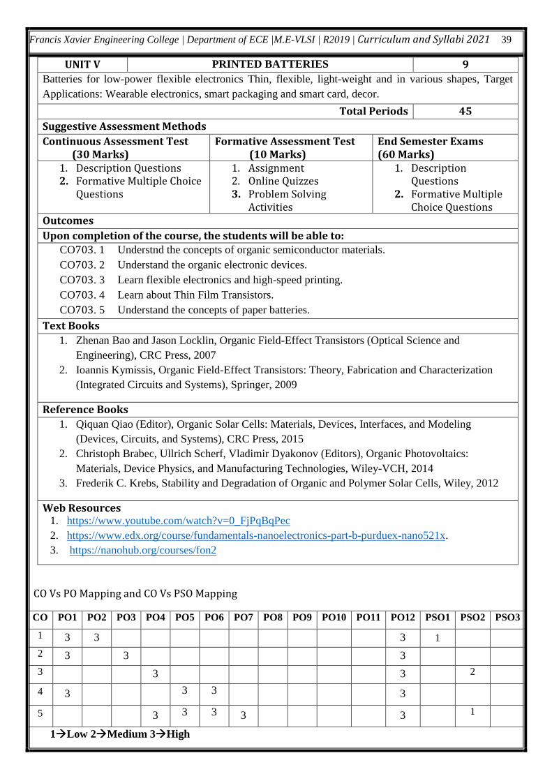
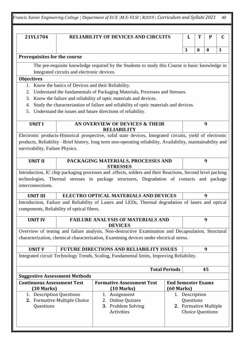
CO PO1 PO2 PO3 PO4 PO5 PO6 PO7 PO8 PO9 PO10 PO11 PO12 PSO1 PSO2 PSO3
1 3 3 3 1
2 3 3 3
3 3 3 2
4 3 3 3 3
5 3 3 3 3 3 1
Francis Xavier Engineering College | Department of ECE |M.E-VLSI | R2019 | Curriculum and Syllabi 2021 40
21VL1704 RELIABILITY OF DEVICES AND CIRCUITS L T P C
3 0 0 3
Prerequisites for the course
The pre-requisite knowledge required by the Students to study this Course is basic knowledge in
Integrated circuits and electronic devices.
Objectives
1. Know the basics of Devices and their Reliability.
2. Understand the fundamentals of Packaging Materials, Processes and Stresses.
3. Know the failure and reliability of optic materials and devices.
4. Study the characteriastion of failure and reliability of optic materials and devices.
5. Understand the issues and future directions of reliability.
UNIT I AN OVERVIEW OF DEVICES & THEIR
RELIABILITY 9
Electronic products-Historical prospective, solid state devices, Integrated circuits, yield of electronic
products, Reliability –Brief history, long term non-operating reliability, Availability, maintainability and
survivability, Failure Physics.
UNIT II PACKAGING MATERIALS, PROCESSES AND
STRESSES 9
Introduction, IC chip packaging processes and .effects, solders and their Reactions, Second level packing
technologies, Thermal stresses in package structures, Degradation of contacts and package
interconnections.
UNIT III ELECTRO OPTICAL MATERIALS AND DEVICES 9
Introduction, Failure and Reliability of Lasers and LEDs, Thermal degradation of lasers and optical
components, Reliability of optical fibers.
UNIT IV FAILURE ANALYSIS OF MATERIALS AND
DEVICES 9
Overview of testing and failure analysis, Non-destructive Examination and Decapsulation, Structural
characterization, chemical characterization, Examining devices under electrical stress.
UNIT V FUTURE DIRECTIONS AND RELIABILITY ISSUES 9
Integrated circuit Technology Trends, Scaling, Fundamental limits, Improving Reliability.
Total Periods 45
Suggestive Assessment Methods
Continuous Assessment Test (30 Marks)
Formative Assessment Test (10 Marks)
End Semester Exams (60 Marks)
1. Description Questions 2. Formative Multiple Choice
Questions
1. Assignment 2. Online Quizzes 3. Problem Solving
Activities
1. Description Questions
2. Formative Multiple Choice Questions
Francis Xavier Engineering College | Department of ECE |M.E-VLSI | R2019 | Curriculum and Syllabi 2021 41
Outcomes
Upon completion of the course, the students will be able to:
CO704. 1 Discuss the fundamentals of Devices and their Reliability
CO704. 2 Explains the fundamentals of Packaging Materials, Processes and Stresses
CO704. 3 Describe the failure and reliability of optic materials and devices.
CO704. 4 Summarize the characteriastion of failure and reliability of optic materials and
devices.
CO704. 5 Explain the issues and future directions of reliability.
Text Books
1. M. Ohring, Reliability and Failure of Electronic Materials and Devices, First Edition, Academic Press,
1998.
2. J.W. McPherson, Reliability Physics and Engineering, Second Edition, Springer, 2013.
3. Yuan Taur and T. Ning, “Fundamentals of Modern VLSI Devices,” Cambridge University Press, 1998.
4. J.Ross, Microelectronic Failure Analysis, Sixth Edition, ASTM International, 2011.
Reference Books 1. Behzad Razavi, “Design of Analog CMOS Integrated Circuits”, Tata McGraw-Hill, 2002.
Web Resources 1. https://nptel.ac.in/courses/117/106/117106091/
2. https://m.eet.com/media/1120313/ic%20wearout%20edn%20v1-1%20%282%29.pdf
3. https://www.sciencedirect.com/book/9780120885749/reliability-and-failure-of-electronic-
materials-and-devices
CO Vs PO Mapping and CO Vs PSO Mapping
1Low 2Medium 3High
CO PO1 PO2 PO3 PO4 PO5 PO6 PO7 PO8 PO9 PO10 PO11 PO12 PSO1 PSO2 PSO3
1 3 3 3 2
2 3 3 3
3 3 3 3
4 3 3 3 3 3
5 3 3 3 3 3 3 1
Francis Xavier Engineering College | Department of ECE |M.E-VLSI | R2019 | Curriculum and Syllabi 2021 42
PROFESSIONAL ELECTIVE II
21VL1705 Graph Theory and Algorithms for CAD 3 0 0 3
21VL1706 Communication Buses and Interfaces 3 0 0 3
21VL1707 Mixed Signal Design 3 0 0 3
21VL1708 VLSI Architectural Design and Implementation 3 0 0 3
21VL1705 GRAPH THEORY AND ALGORITHMS FOR CAD L T P C
3 0 0 3
Prerequisites for the course
The pre-requisite knowledge required by the Students to study this Course is basic knowledge in
CMOS VLSI Design.
Objectives
1. To learn graph theory concepts in VLSI Design.
2. To study the design rules and implement the Layout with proper placement and partitioning
algorithm
3. To learn algorithms to perform Floor planning
4. To understand VLSI design automation tools
5. To study modelling and simulation.
UNIT I GRAPH THEORY 9
Basic Definitions and Examples – Trees and their Characterization – Euler Circuits – Long Paths and
Cycles – Vertex Colourings – Edge Colourings – Vizing's Theorem – Planar Graphs –Including Euler's
Formula– Dual Graphs -Data structures for graph representations – Applications in CAD for VLSI-
Algorithms - Spanning tree algorithms and shortest path algorithms.
UNIT II COMPUTATIONAL COMPLEXITY OF
ALGORITHMS 9
Tractable and Intractable problems, General purpose methods for combinatorial optimization. Big-O
notation- Class P- class NP -NP-hard- NP-complete.
UNIT III LAYOUT AND PARTITIONING 9
Layout Compaction, Design rules, Problem formulation, Algorithms for constraint graph compaction,
Problem formulation- Group Migration Algorithm: Kernighan-Lin Simulated annealing based
Partitioning.
UNIT IV PIN ASSIGNMENT AND PLACEMENT 9
Pin Assignment: Concentric circle mapping, Topological pin assignment- Power and ground routing.
Placement: Wire length estimation models for placement - Quadratic placement- Sequence pair
technique
UNIT V SIMULATION AND LOGIC SYNTHESIS 9
Simulation, Gate-level modelling and simulation, Switch-level modelling and simulation, Combinational
Logic Synthesis, Binary Decision Diagrams, Two Level Logic Synthesis. High-level synthesis-
allocation, assignment and scheduling, scheduling algorithms, Assignment problem, High level
transformations.
Total Periods 45
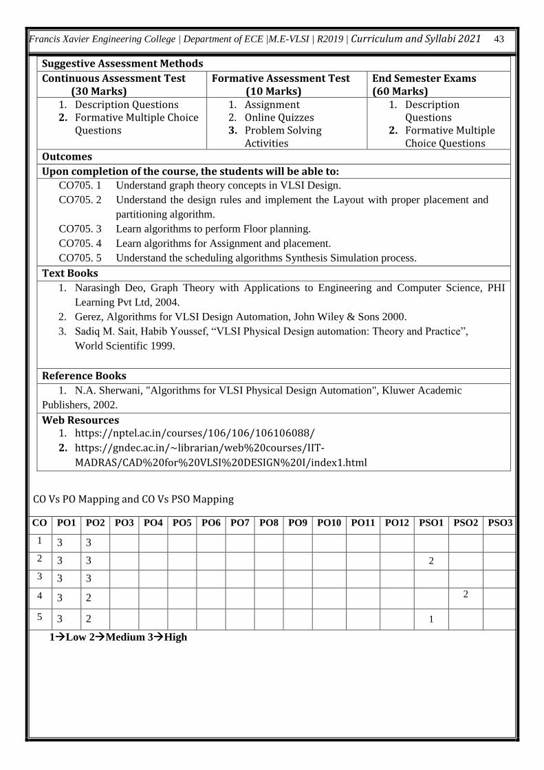
Francis Xavier Engineering College | Department of ECE |M.E-VLSI | R2019 | Curriculum and Syllabi 2021 43
Suggestive Assessment Methods
Continuous Assessment Test (30 Marks)
Formative Assessment Test (10 Marks)
End Semester Exams (60 Marks)
1. Description Questions 2. Formative Multiple Choice
Questions
1. Assignment 2. Online Quizzes 3. Problem Solving
Activities
1. Description Questions
2. Formative Multiple Choice Questions
Outcomes
Upon completion of the course, the students will be able to:
CO705. 1 Understand graph theory concepts in VLSI Design.
CO705. 2 Understand the design rules and implement the Layout with proper placement and
partitioning algorithm.
CO705. 3 Learn algorithms to perform Floor planning.
CO705. 4 Learn algorithms for Assignment and placement.
CO705. 5 Understand the scheduling algorithms Synthesis Simulation process.
Text Books
1. Narasingh Deo, Graph Theory with Applications to Engineering and Computer Science, PHI
Learning Pvt Ltd, 2004.
2. Gerez, Algorithms for VLSI Design Automation, John Wiley & Sons 2000.
3. Sadiq M. Sait, Habib Youssef, “VLSI Physical Design automation: Theory and Practice”,
World Scientific 1999.
Reference Books
1. N.A. Sherwani, "Algorithms for VLSI Physical Design Automation", Kluwer Academic
Publishers, 2002.
Web Resources 1. https://nptel.ac.in/courses/106/106/106106088/
2. https://gndec.ac.in/~librarian/web%20courses/IIT-
MADRAS/CAD%20for%20VLSI%20DESIGN%20I/index1.html
CO Vs PO Mapping and CO Vs PSO Mapping
1Low 2Medium 3High
CO PO1 PO2 PO3 PO4 PO5 PO6 PO7 PO8 PO9 PO10 PO11 PO12 PSO1 PSO2 PSO3
1 3 3
2 3 3 2
3 3 3
4 3 2 2
5 3 2 1
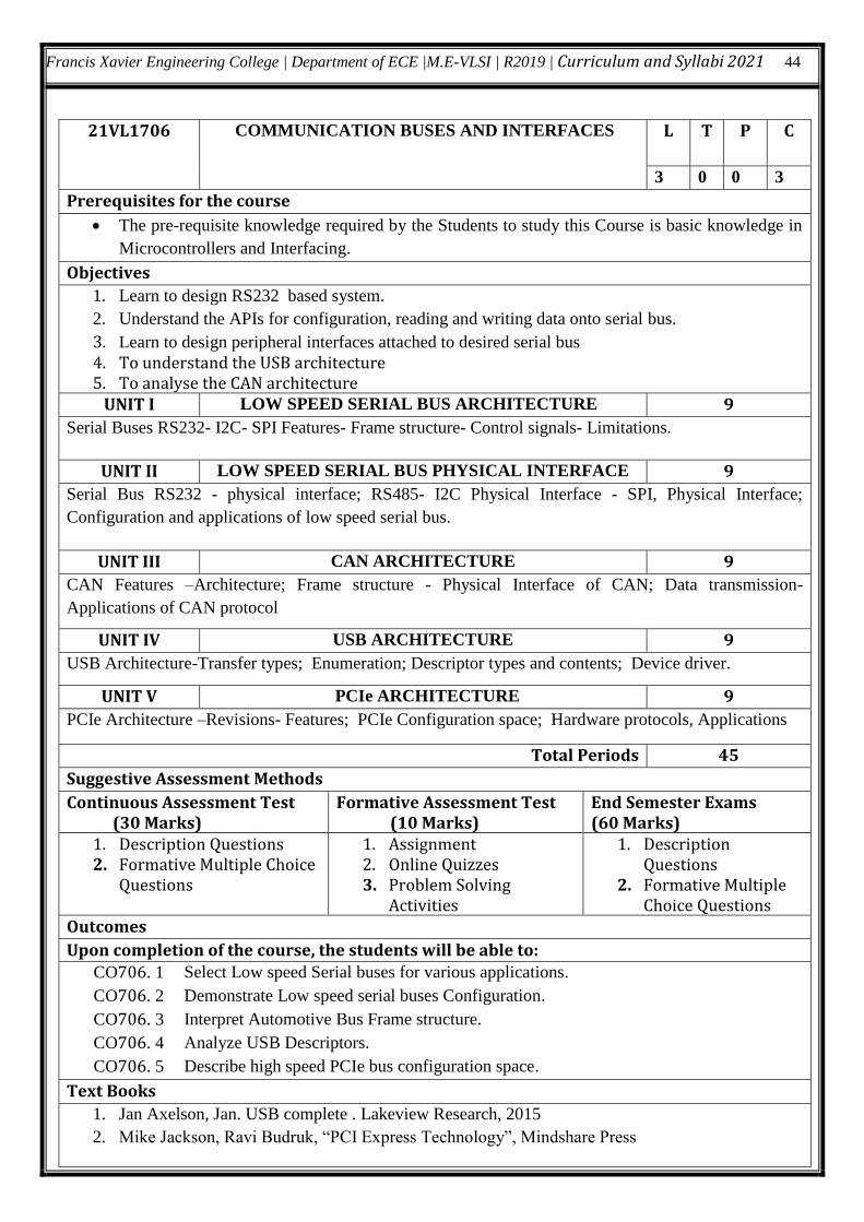
Francis Xavier Engineering College | Department of ECE |M.E-VLSI | R2019 | Curriculum and Syllabi 2021 44
21VL1706 COMMUNICATION BUSES AND INTERFACES L T P C
3 0 0 3
Prerequisites for the course
The pre-requisite knowledge required by the Students to study this Course is basic knowledge in
Microcontrollers and Interfacing.
Objectives
1. Learn to design RS232 based system.
2. Understand the APIs for configuration, reading and writing data onto serial bus.
3. Learn to design peripheral interfaces attached to desired serial bus 4. To understand the USB architecture 5. To analyse the CAN architecture
UNIT I LOW SPEED SERIAL BUS ARCHITECTURE 9
Serial Buses RS232- I2C- SPI Features- Frame structure- Control signals- Limitations.
UNIT II LOW SPEED SERIAL BUS PHYSICAL INTERFACE 9
Serial Bus RS232 - physical interface; RS485- I2C Physical Interface - SPI, Physical Interface;
Configuration and applications of low speed serial bus.
UNIT III CAN ARCHITECTURE 9
CAN Features –Architecture; Frame structure - Physical Interface of CAN; Data transmission-
Applications of CAN protocol
UNIT IV USB ARCHITECTURE 9
USB Architecture-Transfer types; Enumeration; Descriptor types and contents; Device driver.
UNIT V PCIe ARCHITECTURE 9
PCIe Architecture –Revisions- Features; PCIe Configuration space; Hardware protocols, Applications
Total Periods 45
Suggestive Assessment Methods
Continuous Assessment Test (30 Marks)
Formative Assessment Test (10 Marks)
End Semester Exams (60 Marks)
1. Description Questions 2. Formative Multiple Choice
Questions
1. Assignment 2. Online Quizzes 3. Problem Solving
Activities
1. Description Questions
2. Formative Multiple Choice Questions
Outcomes
Upon completion of the course, the students will be able to:
CO706. 1 Select Low speed Serial buses for various applications.
CO706. 2 Demonstrate Low speed serial buses Configuration.
CO706. 3 Interpret Automotive Bus Frame structure.
CO706. 4 Analyze USB Descriptors.
CO706. 5 Describe high speed PCIe bus configuration space.
Text Books
1. Jan Axelson, Jan. USB complete . Lakeview Research, 2015
2. Mike Jackson, Ravi Budruk, “PCI Express Technology”, Mindshare Press
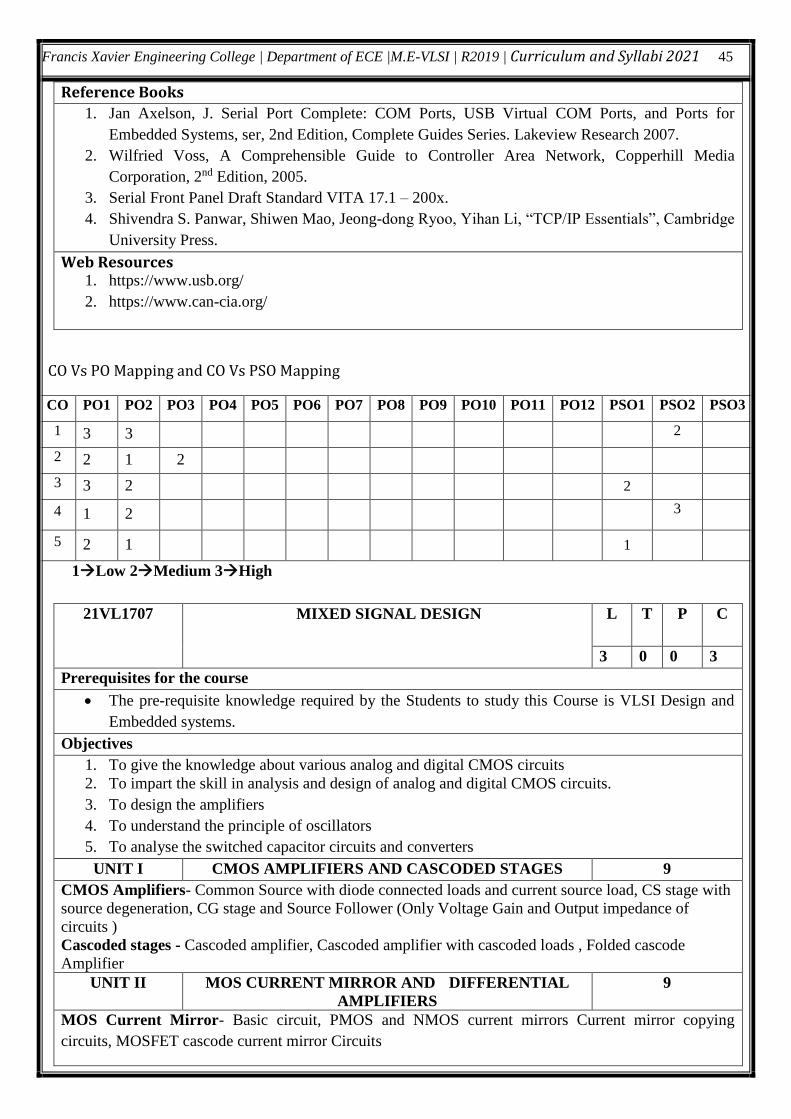
Francis Xavier Engineering College | Department of ECE |M.E-VLSI | R2019 | Curriculum and Syllabi 2021 45
Reference Books
1. Jan Axelson, J. Serial Port Complete: COM Ports, USB Virtual COM Ports, and Ports for
Embedded Systems, ser, 2nd Edition, Complete Guides Series. Lakeview Research 2007.
2. Wilfried Voss, A Comprehensible Guide to Controller Area Network, Copperhill Media
Corporation, 2nd Edition, 2005.
3. Serial Front Panel Draft Standard VITA 17.1 – 200x.
4. Shivendra S. Panwar, Shiwen Mao, Jeong-dong Ryoo, Yihan Li, “TCP/IP Essentials”, Cambridge
University Press.
Web Resources 1. https://www.usb.org/
2. https://www.can-cia.org/
CO Vs PO Mapping and CO Vs PSO Mapping
1Low 2Medium 3High
21VL1707 MIXED SIGNAL DESIGN L T P C
3 0 0 3
Prerequisites for the course
The pre-requisite knowledge required by the Students to study this Course is VLSI Design and
Embedded systems.
Objectives
1. To give the knowledge about various analog and digital CMOS circuits
2. To impart the skill in analysis and design of analog and digital CMOS circuits.
3. To design the amplifiers
4. To understand the principle of oscillators
5. To analyse the switched capacitor circuits and converters
UNIT I CMOS AMPLIFIERS AND CASCODED STAGES 9
CMOS Amplifiers- Common Source with diode connected loads and current source load, CS stage with
source degeneration, CG stage and Source Follower (Only Voltage Gain and Output impedance of
circuits )
Cascoded stages - Cascoded amplifier, Cascoded amplifier with cascoded loads , Folded cascode
Amplifier
UNIT II MOS CURRENT MIRROR AND DIFFERENTIAL
AMPLIFIERS
9
MOS Current Mirror- Basic circuit, PMOS and NMOS current mirrors Current mirror copying
circuits, MOSFET cascode current mirror Circuits
CO PO1 PO2 PO3 PO4 PO5 PO6 PO7 PO8 PO9 PO10 PO11 PO12 PSO1 PSO2 PSO3
1 3 3 2
2 2 1 2
3 3 2 2
4 1 2 3
5 2 1 1
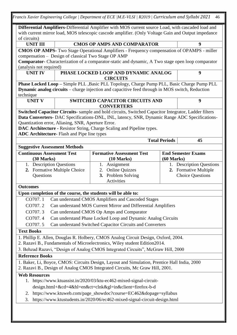
Francis Xavier Engineering College | Department of ECE |M.E-VLSI | R2019 | Curriculum and Syllabi 2021 46
Differential Amplifiers-Differential Amplifier with MOS current source Load, with cascaded load and
with current mirror load, MOS telescopic cascode amplifier. (Only Voltage Gain and Output impedance
of circuits)
UNIT III CMOS OP AMPS AND COMPARATOR 9
CMOS OP AMPS- Two Stage Operational Amplifiers - Frequency compensation of OPAMPS - miller
compensation – Design of classical Two Stage OP AMP
Comparator- Characterization of a comparator-static and dynamic, A Two stage open loop comparator
(analysis not required)
UNIT IV PHASE LOCKED LOOP AND DYNAMIC ANALOG
CIRCUITS
9
Phase Locked Loop – Simple PLL ,Basic PLL Topology, Charge Pump PLL, Basic Charge Pump PLL
Dynamic analog circuits – charge injection and capacitive feed through in MOS switch, Reduction
technique
UNIT V SWITCHED CAPACITOR CIRCUITS AND
CONVERTERS
9
Switched Capacitor Circuits- sample and hold circuits, Switched Capacitor Integrator, Ladder filters
Data Converters- DAC Specifications-DNL, INL, latency, SNR, Dynamic Range ADC Specifications-
Quantization error, Aliasing, SNR, Aperture Error.
DAC Architecture - Resistor String, Charge Scaling and Pipeline types.
ADC Architecture- Flash and Pipe line types
Total Periods 45
Suggestive Assessment Methods
Continuous Assessment Test
(30 Marks)
Formative Assessment Test
(10 Marks)
End Semester Exams
(60 Marks)
1. Description Questions
2. Formative Multiple Choice
Questions
1. Assignment
2. Online Quizzes
3. Problem Solving
Activities
1. Description Questions
2. Formative Multiple
Choice Questions
Outcomes
Upon completion of the course, the students will be able to:
CO707. 1 Can understand CMOS Amplifiers and Cascoded Stages
CO707. 2 Can understand MOS Current Mirror and Differential Amplifiers
CO707. 3 Can understand CMOS Op Amps and Comparator
CO707. 4 Can understand Phase Locked Loop and Dynamic Analog Circuits
CO707. 5 Can understand Switched Capacitor Circuits and Converters
Text Books
1. Phillip E. Allen, Douglas R. Holbery, CMOS Analog Circuit Design, Oxford, 2004.
2. Razavi B., Fundamentals of Microelectronics, Wiley student Edition2014.
3. Behzad Razavi, “Design of Analog CMOS Integrated Circuits”, McGraw Hill, 2000
Reference Books
1. Baker, Li, Boyce, CMOS: Circuits Design, Layout and Simulation, Prentice Hall India, 2000
2. Razavi B., Design of Analog CMOS Integrated Circuits, Mc Graw Hill, 2001.
Web Resources
1. https://www.ktuassist.in/2020/03/ktu-ec462-mixed-signal-circuit-
design.html+&cd=4&hl=en&ct=clnk&gl=in&client=firefox-b-d
2. https://www.ktuweb.com/page_showdoc?course=EC462&dopage=syllabus
3. https://www.ktustudents.in/2020/06/ec462-mixed-signal-circuit-design.html
Francis Xavier Engineering College | Department of ECE |M.E-VLSI | R2019 | Curriculum and Syllabi 2021 47
CO Vs PO Mapping and CO Vs PSO Mapping
1Low 2Medium 3High
21VL1708 VLSI ARCHITECTURAL DESIGN AND
IMPLEMENTATION
L T P C
3 0 0 3
Prerequisites for the course
The pre-requisite knowledge required by the Students to study this Course is basic knowledge in
CMOS VLSI Design.
Objectives
1. To review the architectural design of VLSI systems as seen in complex SoCs.
2. To learn performance optimization techniques in VLSI signal processing.
3. To understand the design of synchronous clocking and flow of asynchronous data processing.
4. To understand the VLSI circuit floorplan and chip assembly.
5. To understand the physical design and verification
UNIT I INTRODUCTION TO VLSI ARCHITECTURE 9 Introduction: Review of VLSI Design flow. Goals of VLSI Design: Optimization of speed, power dissipation, cost
and reliability - Algorithm to architecture transformation: Architectural antipodes, transform approach to
VLSI architectures, graph based formalism for describing processing algorithms, isomorphic architecture
- Equivalence transforms for combinational computations: Common assumptions, pipelining, replication,
time sharing, associatively transform and other algebraic transforms
UNIT II ARCHITECTURAL SYNTHESIS AND
OPTIMIZATION 9
Architectural Synthesis and Optimization: Circuit specifications for architectural synthesis, fundamental
architectural synthesis problems, temporal domain-scheduling, spatial domain binding, sequencing
graphs, hierarchical models, synchronization problem, area and performance estimation, data path and
control unit synthesis, constrained and unconstrained scheduling, scheduling of pipelined circuits
UNIT III DESIGN & CLOCKING OF SYNCHRONOUS
CIRCUITS 9
The grand alternatives for regulating state changes - Why a rigorous approach to clocking is essential in VLSI -
The dos and don’ts of synchronous circuit design - Clocking of Synchronous Circuits: difficulty in clock
distribution - skew and jitter within tight bounds - Input/output timing - Clock gating properly
UNIT IV ASYNCHRONOUS DATA PROCESSING
ARCHITECTURES 9
Data consistency problem of vectored acquisition-plain bit parallel synchronization, Unit distance coding,
Suppression of cross patterns, handshaking, partial handshaking, Data consistency problem of scalar acquisition-
synchronization at single place, Synchronization at multiple places, Synchronization from a slow clock,
Metastable synchronizer behaviour- Energy Efficiency and Heat Removal: Energy dissipated in CMOS circuits -
How to improve energy efficiency - Heat flow and heat removal
CO PO1 PO2 PO3 PO4 PO5 PO6 PO7 PO8 PO9 PO10 PO11 PO12 PSO1 PSO2 PSO3
1 3 2
2 3 1 3 2
3 2 2 3
4 3 3 2 2
5 2 1
Francis Xavier Engineering College | Department of ECE |M.E-VLSI | R2019 | Curriculum and Syllabi 2021 48
UNIT V PHYSICAL DESIGN & VERIFICATION 9
Conducting layers and their characteristics - Cell-based back-end design - Floorplanning -Identify major
building blocks and clock domains - Establish a pin budget- Find a relative arrangement of all major
building blocks - Plan power, clock, and signal distribution - Place and route (P&R) - Chip assembly
Total Periods 45
Suggestive Assessment Methods
Continuous Assessment Test (30 Marks)
Formative Assessment Test (10 Marks)
End Semester Exams (60 Marks)
1. Description Questions 2. Formative Multiple Choice
Questions
1. Assignment 2. Online Quizzes 3. Problem Solving
Activities
1. Description Questions
2. Formative Multiple Choice Questions
Outcomes
Upon completion of the course, the students will be able to:
CO708. 1 Understand transformation of VLSI from Algorithm to architecture.
CO708. 2 Analysis VLSI architectural synthsis and optimization.
CO708. 3 Design synchrouous clocking circuits
CO708. 4 Understand the process flow of asynchronous data.
CO708. 5 Get Strong foundation in VLSI circuit floorplanning and chip design.
Text Books
1. Hubert Kaeslin, “Digital Integrated Circuit Design: From VLSI Architectures to CMOS
Fabrication”, Cambridge University Press (2009).
2. Giovanni De Micheli, “Synthesis and Optimization of Digital Circuits”, McGraw Hill (2012).
Reference Books
1. Peter Pirsch, "Architectures for Digital Signal Processing", John Willy & sons,2nd Edition,2014.
2. Behrooz Parhami, " Computer Arithmetic: Algorithm and Hardware Design", Behrooz Parhami,
Oxford University Press, 2nd Edition, 2009.
Web Resources 1. https://nptel.ac.in/courses/108/105/108105118/
2. https://designnation.in/an-overview-on-vlsi-design-with-its-example/
3. https://www.youtube.com/watch?v=cIlwGFcDLhI
CO Vs PO Mapping and CO Vs PSO Mapping
1Low 2Medium 3High
CO PO1 PO2 PO3 PO4 PO5 PO6 PO7 PO8 PO9 PO10 PO11 PO12 PSO1 PSO2 PSO3
1 3 2 2 2
2 3 3 2 2 2
3 3 2 3 2
4 3 2 3 2 3
5 3 3 2 1
Francis Xavier Engineering College | Department of ECE |M.E-VLSI | R2019 | Curriculum and Syllabi 2021 49
PROFESSIONAL ELECTIVE III
21VL2701 VLSI Signal Processing 3 0 0 3
21VL2702 Scripting Languages for VLSI 3 0 0 3
21VL2703 Advanced Memory Technologies 3 0 0 3
21VL2704 System on Chip Design 3 0 0 3
21VL2701 VLSI SIGNAL PROCESSING L T P C
3 0 0 3
Prerequisites for the course
Analog and Digital IC
Objectives
1. To familiarize various representation methods of DSP algorithms, understand the significance of
the iteration bound and to calculate the same for a given single-rate and/or multi-rate DFG.
2. To understand retiming and pipelining and parallel processing.
3. To understand algorithms unfolding and folding on a given DFG.
4. To understand the concepts of fast convolution, pipelining and parallel processing for FIR and
IIR filters
5. To signify and calculate the effects of numerical strength reduction, scaling and round-off noise
for a given digital filter with limited word length.
UNIT I INTRODUCTION TO SIGNAL PROCESSING 9
Typical DSP Algorithms – DSP Application Demands and Scaled CMOS Technologies -
Representations of DSP Algorithms - Data-Flow Graph Representations. Introduction -Loop Bound and
Iteration Bound -Algorithms for Computing Iteration Bound: Longest Path Matrix and Multiple Cycle
Mean algorithms - Iteration Bound of Multi-rate Data Flow Graphs.
UNIT II PIPELINING, PARALLEL PROCESSING AND
RETIMING 9
Pipelining, Parallel processing and Retiming- Introduction to Retiming -Definitions and Properties -
Solving Systems of Inequalities - The Bellman-Ford Algorithm - The Floyd Warshall Algorithm-
Retiming Techniques.
UNIT III UNFOLDING AND FOLDING 9
Introduction, An Algorithm for Unfolding, Properties of Unfolding, Critical Path, Unfolding, and
Retiming, Applications of Unfolding, Introduction, Folding Transformation, Register Minimization
Techniques, Register Minimization in Folded Architectures.
UNIT IV FAST CONVOLUTION, PIPELINING AND
PARALLEL PROCESSING FOR FIR AND IIR
FILTERS
9
Fast convolution – Cook-Toom algorithm, modified Cook-Toom algorithm, Pipelined and parallel
recursive filters – Look-Ahead pipelining in first-order IIR filters, Look-Ahead pipelining with power-
of-2 decomposition, Clustered look-ahead pipelining, Parallel processing of IIR filters, combined
pipelining and parallel processing of IIR filters.
Francis Xavier Engineering College | Department of ECE |M.E-VLSI | R2019 | Curriculum and Syllabi 2021 50
UNIT V NUMERICAL STRENGTH REDUCTION, SCALING
AND ROUNDING NOISE 9
Introduction, Numerical strength reduction – subexpression elimination, multiple constant multiplication,
Scaling and Rounding Noise, State Variable Description of Digital Filters, Scaling and Rounding Noise
Computation, Rounding Noise in Pipelined IIR Filters.
Total Periods 45
Suggestive Assessment Methods
Continuous Assessment Test (30 Marks)
Formative Assessment Test (10 Marks)
End Semester Exams (60 Marks)
1. Description Questions 2. Formative Multiple Choice
Questions
1. Assignment 2. Online Quizzes 3. Problem Solving
Activities
1. Description Questions
2. Formative Multiple Choice Questions
Outcomes
Upon completion of the course, the students will be able to:
CO701. 1 Compare various representation methods of DSP algorithms and find iteration bound of a
given single and/or multi-rate DFG.
CO701. 2 Understand and transform the given DFG using retiming with constraints and pipelining and
parallel processing.
CO701. 3 Apply unfolding and folding on the given DFG.
CO701. 4 Understand concepts of fast convolution, pipelining and parallel processing for FIR and IIR
filters
CO701. 5 Understand and apply algorithmic and numerical strength reduction methods and calculate
scaling and round-off noise of the given digital filter with limited word length.
Text Books
1. Keshab K. Parhi, VLSI Digital Signal Processing Systems: Design and Implementation,
Reprint, Wiley, Inter Science, 2014.
2. John G. Proakis, Dimitris K Manolakis, Digital Signal Processing: Principles, Algorithms and
Applications, Prentice Hall, Fourth Edition, 2015.
3. Mohammed Ismail and Terri Fiez, Analog VLSI Signal and Information Processing, McGraw-
Hill, 2014.
4. S.Y. Kung, H.J. White House, T. Kailath, VLSI and Modern Signal Processing, PHI, 2010.
5. S. K. Mitra, Digital Signal Processing –A Computer Based Approach, Fourth Edition, McGraw-
Hill, 2010.
Reference Books
Web Resources 1. https://nptel.ac.in/courses/108/105/108105157/
2. https://www.wiley.com/en-us/
VLSI+Digital+Signal+Processing+Systems%3A+Design+and+Implementation-p-
9780471241867
3. https://www.classcentral.com/course/swayam-vlsi-signal-processing-17837
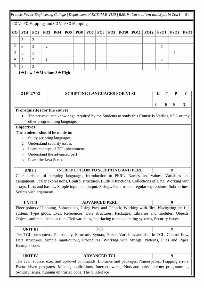
Francis Xavier Engineering College | Department of ECE |M.E-VLSI | R2019 | Curriculum and Syllabi 2021 51
CO Vs PO Mapping and CO Vs PSO Mapping
1Low 2Medium 3High
21VL2702 SCRIPTING LANGUAGES FOR VLSI L T P C
3 0 0 3
Prerequisites for the course
The pre-requisite knowledge required by the Students to study this Course is Verilog HDL or any
other programming language.
Objectives
The students should be made to:
1. Study scripting languages
2. Understand security issues
3. Learn concept of TCL phenomena
4. Understand the advanced perl
5. Learn the Java Script
UNIT I INTRODUCTION TO SCRIPTING AND PERL 9
Characteristics of scripting languages, Introduction to PERL, Names and values, Variables and
assignment, Scalar expressions, Control structures, Built-in functions, Collections of Data, Working with
arrays, Lists and hashes, Simple input and output, Strings, Patterns and regular expressions, Subroutines,
Scripts with arguments.
UNIT II ADVANCED PERL 9
Finer points of Looping, Subroutines, Using Pack and Unpack, Working with files, Navigating the file
system, Type globs, Eval, References, Data structures, Packages, Libraries and modules, Objects,
Objects and modules in action, Tied variables, Interfacing to the operating systems, Security issues.
UNIT III TCL 9
The TCL phenomena, Philosophy, Structure, Syntax, Parser, Variables and data in TCL, Control flow,
Data structures, Simple input/output, Procedures, Working with Strings, Patterns, Files and Pipes,
Example code.
UNIT IV ADVANCED TCL 9
The eval, source, exec and up-level commands, Libraries and packages, Namespaces, Trapping errors,
Event-driven programs, Making applications 'Internet-aware', 'Nuts-and-bolts' internet programming,
Security issues, running un trusted code, The C interface
CO PO1 PO2 PO3 PO4 PO5 PO6 PO7 PO8 PO9 PO10 PO11 PO12 PSO1 PSO2 PSO3
1 3 3
2 3 3 2 2
3 3 3 1
4 3 2 1 2
5 3 2
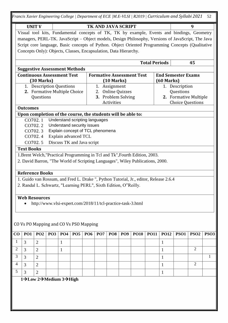
Francis Xavier Engineering College | Department of ECE |M.E-VLSI | R2019 | Curriculum and Syllabi 2021 52
UNIT V TK AND JAVA SCRIPT 9
Visual tool kits, Fundamental concepts of TK, TK by example, Events and bindings, Geometry
managers, PERL-TK. JavaScript – Object models, Design Philosophy, Versions of JavaScript, The Java
Script core language, Basic concepts of Python. Object Oriented Programming Concepts (Qualitative
Concepts Only): Objects, Classes, Encapsulation, Data Hierarchy.
Total Periods 45
Suggestive Assessment Methods
Continuous Assessment Test (30 Marks)
Formative Assessment Test (10 Marks)
End Semester Exams (60 Marks)
1. Description Questions 2. Formative Multiple Choice
Questions
1. Assignment 2. Online Quizzes 3. Problem Solving
Activities
1. Description Questions
2. Formative Multiple Choice Questions
Outcomes
Upon completion of the course, the students will be able to:
CO702. 1 Understand scripting languages
CO702. 2 Understand security issues
CO702. 3 Explain concept of TCL phenomena
CO702. 4 Explain advanced TCL
CO702. 5 Discuss TK and Java script
Text Books
1.Brent Welch,"Practical Programming in Tcl and Tk",Fourth Edition, 2003.
2. David Barron, "The World of Scripting Languages", Wiley Publications, 2000.
Reference Books
1. Guido van Rossum, and Fred L. Drake ", Python Tutorial, Jr., editor, Release 2.6.4
2. Randal L. Schwartz, "Learning PERL", Sixth Edition, O‟Reilly.
Web Resources http://www.vlsi-expert.com/2018/11/tcl-practice-task-3.html
CO Vs PO Mapping and CO Vs PSO Mapping
1Low 2Medium 3High
CO PO1 PO2 PO3 PO4 PO5 PO6 PO7 PO8 PO9 PO10 PO11 PO12 PSO1 PSO2 PSO3
1 3 2 1 1
2 3 2 1 1 2
3 3 2 1 1
4 3 2 1 2
5 3 2 1
Francis Xavier Engineering College | Department of ECE |M.E-VLSI | R2019 | Curriculum and Syllabi 2021 53
21VL2703 ADVANCED MEMORY TECHNOLOGIES L T P C
3 0 0 3
Prerequisites for the course
CMOS VLSI Design
Objectives
1. Expounding the basics and detailed architecture of SRAMs and DRAMs.
2. Model the memory fault and introduce the basic and advanced memory testing patterns.
3. To get an overview on reliability of semiconductors.
4. Review and discuss high performance memory subsystems, advanced memory technologies and
contemporary issues.
5. To understand the advanced memory technologies
UNIT I RANDOM ACCESS MEMORY TECHNOLOGIES 9
SRAM Cell Structures, MOS SRAM Architecture, MOS SRAM Cell and Peripheral Circuit Operation,
Bipolar SRAM Technologies-Silicon On Insulator (SOl) Technology Operation, Advanced SRAM
Architectures and Technologies-Application Specific SRAMs, DRAM Technology Development-CMOS
DRAMs, DRAMs Cell Theory and Advanced Cell Strucutures - BiCMOS, DRAMs, Soft Error Failures
in DRAMs, Advanced DRAM Designs and Architecture-Application Specific DRAMs
UNIT II NONVOLATILE MEMORIES 9
Masked Read-Only Memories (ROMs) - High Density ROMs, Programmable Read-Only Memories
(PROMs) - BipolarPROMs-CMOS PROMs, Erasable (UV) - Programmable Road-Only Memories
(EPROMs) - Floating-Gate EPROM Cell-One-Time Programmable (OTP) Eproms- Electrically Erasable
PROMs (EEPROMs)-EEPROM Technology And Architecture, Nonvolatile SRAM, Flash Memories
(EPROMs or EEPROM), Advanced Flash Memory Architecture.
UNIT III MEMORY FAULT MODELING AND TESTING 9
RAM Fault Modelling, Electrical Testing, Peusdo Random Testing-Megabit DRAM Testing, Non-
volatile Memory Modelling and Testing, IDDQ Fault Modelling and Testing, Application Specific
Memory Testing
UNIT IV SEMICONDUCTOR MEMORY RELIABILITY 9
General Reliability Issues, RAM Failure Modes and Mechanism, Non-volatile Memory Reliability,
Reliability Modelling and Failure Rate Prediction, Design for Reliability, Reliability Test Structures,
Reliability Screening and Qualification.
UNIT V ADVANCED MEMORY TECHNOLOGIES 9
Ferroelectric Random Access Memories (FRAMs), Gallium Arsenide (GaAs) FRAMs, Analog
Memories-Magneto-resistive Random Access Memories (MRAMs), Experimental Memory Devices.
Memory Hybrids and MCMs (2D) - Memory Stacks and MCMs (3D), Memory MCM Testing and
Reliability Issues, Memory Cards, High Density Memory Packaging Future Directions.
Total Periods 45
Suggestive Assessment Methods
Continuous Assessment Test (30 Marks)
Formative Assessment Test (10 Marks)
End Semester Exams (60 Marks)
1. Description Questions 2. Formative Multiple Choice
Questions
1. Assignment 2. Online Quizzes 3. Problem Solving
Activities
1. Description Questions
2. Formative Multiple Choice Questions
Francis Xavier Engineering College | Department of ECE |M.E-VLSI | R2019 | Curriculum and Syllabi 2021 54
Outcomes
Upon completion of the course, the students will be able to:
CO703. 1 Design SRAMs and DRAMs.
CO703. 2 Design NVRAMs and Flash Memories..
CO703. 3 Model memory faults, select suitable testing patterns and develop testing patterns.
CO703. 4 Improve the reliability of semiconductor memories.
CO703. 5 Contribute to the development of high performance memory subsystems and use
advanced memory technologies.
Text Books
1. Ashok K. Sharma, “Semiconductor Memories: Technology Testing and Reliability" Prentice Hall
of India”, 2007.
2. Ashok K. Sharma, “Semiconductor Memories Two Volume Set”, Wiley, IEEE Press 2003.
Reference Books
1. Brent Keeth, R. Jacob Baker, Brian Johnson, Freng Lin, "DRAM Circuit Design: Fundamental
and High Speed Topics", Wiley-IEEE Press, Second Edition, 2008
2. Brent Keeth, R. Jacob Baker, “DRAM Circuit Design: A Tutorial”, Wiley, IEEE Press, 2000
3. Betty Prince, "Emerging Memories - Technologies and Trends", Kluwer Academic Publishers,
2002.
Web Resources 1. Memory Technology, https://www.sciencedirect.com/topics/computer-science/memory-
technology
2. Reliability of Semiconductor Memories from a Practical Point of View,
https://link.springer.com/chapter/10.1007%2F978-3-322-83629-8_22
3. Advanced memory—Materials for a new era of information technology,
https://doi.org/10.1557/mrs.2018.96
CO Vs PO Mapping and CO Vs PSO Mapping
1Low 2Medium 3High
CO PO1 PO2 PO3 PO4 PO5 PO6 PO7 PO8 PO9 PO10 PO11 PO12 PSO1 PSO2 PSO3
1 3 2 3
2 2 2 3 2
3 2 3 2 1
4 1 1 1
5 2 3 1 2
Francis Xavier Engineering College | Department of ECE |M.E-VLSI | R2019 | Curriculum and Syllabi 2021 55
21VL2704 SYSTEMS ON CHIP DESIGN L T P C
3 0 0 3
Prerequisites for the course
1. Digital electronics
2. System architecture
Objectives
1. To understand concept of Systems-on-Chip
2. To implement SoC on processors.
3. To obtain skills to design SoC using ADL.
4. To develop skills in applying SoC for real time applications
5. To understand the no instruction set computer
UNIT I INTRODUCTION TO SoC DESIGN 9
Architecture of the Present Day SoC-Design Issues of SoC-Hardware Software Codesign-SoC Design
Flow-General Guidelines for Design Reuse-Synchronous Design-Memory and Mixed-Signal Design-On-
Chip Buses-Clock Distribution-Clear/Set/Reset Signals-Physical Design-Design Process for Soft and
Firm Cores-System Integration-Designing With Hard Cores-Designing With Soft Cores
UNIT II PROCESSORS FOR SoC 9
Processor Selection for SOC-Basic Concepts in Processor Architecture-Basic Concepts in Processor
Microarchitecture-Basic Elements in Instruction Handling-Buffers: Minimizing Pipeline Delays-VLIW
Processors-Superscalar Processors-Processor Evolution
UNIT III SoC MEMORY AND INTERCONNECT DESIGN 9
Overview-Scratchpads and Cache Memory-Basic Notion-Cache Organization-Cache Data-Write
Policies-Strategies for Line Replacement at Miss Time-Multilevel Caches-SOC (On-Die) Memory
Systems-Simple DRAM and the Memory Array-Models of Simple Processor–Memory Interactions-
Overview: Interconnect Architectures-Bus: Basic Architecture-SOC Standard Buses
UNIT IV ADL AND NISC 9
Architecture Description Languages (ADL) for design and verification of Application Specific
Instruction set Processors (ASIP), No-Instruction-Set-computer (NISC) - design flow, modeling NISC
architectures and systems, use of Generic Netlist Representation - A formal language for specification,
compilation and synthesis of embedded processors.
UNIT V SoC APPLICATION STUDY 9
SOC Design Approach,-AES-3-D Graphics Processors-Image Compression-Video Compression-Further
Application Studies-Challenges Ahead-Overview-Powering the ASOC-The Shape of the ASOC-
Computer Module and Memory-RF or Light Communications-Pre-Deployment-Post-Deployment
Total Periods 45
Suggestive Assessment Methods
Continuous Assessment Test (30 Marks)
Formative Assessment Test (10 Marks)
End Semester Exams (60 Marks)
1. Description Questions 2. Formative Multiple Choice
Questions
1. Assignment 2. Online Quizzes 3. Problem Solving
Activities
1. Description Questions
2. Formative Multiple Choice Questions
Francis Xavier Engineering College | Department of ECE |M.E-VLSI | R2019 | Curriculum and Syllabi 2021 56
Outcomes
Upon completion of the course, the students will be able to:
CO704. 1 To understand the concept of SoC and its design flow
CO704. 2 To learn and understand implementation of SoC on different processors.
CO704. 3 To learn and understand the memory design and interconnection architecture in SoC
CO704. 4 To learn and implement fault tolerance and monitoring services on NOC
CO704. 5 To apply the SoC concept for various eal time applications.
Text Books
1. RochitRajsuman, “System-on- a-chip: Design and test”, Advantest America R & D center, 2000.
2. P Mishra and N Dutt, “Processor Description Languages”, Morgan Kaufmann, 2008
3. Michael J. Flynn and Wayne Luk, “Computer System Design: System-on-Chip”. Wiley, 2011.
Reference Books
1. Hubert Kaeslin, “Digital Integrated Circuit Design: From VLSI Architectures to CMOS
Fabrication”, Cambridge University Press, 2008.
2. B. Al Hashimi, “System on chip-Next generation electronics”, The IET, 2006
Web Resources 1. https://www.cerc.utexas.edu/~jaa/soc/lectures/1-2.pdf
2. https://www.cl.cam.ac.uk/teaching/1516/SysOnChip/materials.d/socdam-notes00.pdf
3. https://nptel.ac.in/courses/108102045/10
CO Vs PO Mapping and CO Vs PSO Mapping
1Low 2Medium 3High
CO PO1 PO2 PO3 PO4 PO5 PO6 PO7 PO8 PO9 PO10 PO11 PO12 PSO1 PSO2 PSO3
1 1 2 1 2 1 3 2 3
2 1 2 2 2 1 3 2 2
3 1 3 2 1 1 2 1 3 2
4 3 2 1 1 2 1 3 2 3
5 3 2 1 1 2 1 3 2 2
Francis Xavier Engineering College | Department of ECE |M.E-VLSI | R2019 | Curriculum and Syllabi 2021 57
PROFESSIONAL ELECTIVE IV
21VL2705 VLSI Test and Testability 3 0 0 3
21VL2706 VLSI Digital Design Verification 3 0 0 3
21VL2707 Modern Computer Architecture 3 0 0 3
21VL2708 Electronic Design Automation 3 0 0 3
21VL2705 VLSI TEST AND TESTABILITY L T P C
3 0 0 3
Prerequisites for the course
The pre-requisite knowledge required by the Students to study this Course is basic knowledge in
Digital Design and CMOS VLSI DESIGN
Objectives
1. To Identify the significance of testable design
2. To Generate optimized test patterns for combinational and sequential logic circuits
3. To Enables to design for testability
4. To Design scan chains and BIST modules for digital designs
5. To Understand boundary scan based test architectures
UNIT I BASICS OF TEST 9
Design and Test, Test Concerns, HDLs in Digital System Test, ATE Architecture and Instrumentation,
Challenges in VLSI Testing, Levels of Abstraction in VLSI Testing, Historical Review of VLSI Test
Technology, Fault Modeling, Structural Gate Level Faults, Issues Related to Gate Level Faults, Fault
Collapsing
UNIT II TEST PATTERN GENERATION METHODS AND
ALGORITHMS 9
Test Generation Basics, Controllability and Observability, Random Test Generation, Designing a Stuck-
At ATPG for Combinational Circuits, Reed –Muller Expansion Technique, Designing a Sequential
ATPG
UNIT III DESIGN FOR TESTABILITY 9
Design for Testability Basics, Scan Cell Designs, Scan Architectures, Scan Design Rules, Scan Design
Flow, Special-Purpose Scan Designs, Fault Simulation, Combinational Logic Diagnosis, Scan Chain
Diagnosis
UNIT IV BUILT-IN SELF-TEST 9
BIST Design Rules, Test Pattern Generation, Output Response Analysis, Logic BIST Architectures,
Digital Boundary Scan, Boundary Scan for Advanced Networks, Embedded Core Test Standard, IDDQ
Testing , Logic BIST Diagnosis
Francis Xavier Engineering College | Department of ECE |M.E-VLSI | R2019 | Curriculum and Syllabi 2021 58
UNIT V MEMORY TESTING & TEST TECHNOLOGY
TRENDS 9
RAM Functional Fault Models and Test Algorithms, RAM Fault Simulation and Test Algorithm
Generation , Memory Built-In Self-Test, Built-In Self-Repair,Delay Testing, FPGA Testing, MEMS
Testing, High-speed I/O Testing, RF Testing.
Total Periods 45
Suggestive Assessment Methods
Continuous Assessment Test (30 Marks)
Formative Assessment Test (10 Marks)
End Semester Exams (60 Marks)
1. Description Questions 2. Formative Multiple Choice
Questions
1. Assignment 2. Online Quizzes 3. Problem Solving
Activities
1. Description Questions
2. Formative Multiple Choice Questions
Outcomes
Upon completion of the course, the students will be able to:
CO705. 1 To Identify the significance of testable design
CO705. 2 To Generate optimized test patterns for combinational and sequential logic circuits
CO705. 3 To Enables to design for testability
CO705. 4 To Design scan chains and BIST modules for digital designs
CO705. 5 To Understand boundary scan based test architectures
To Analyse the test vector techniques for memory and fault diagnosis.
Text Books
1. Zainalabedin Navabi (auth.) - Digital System Test and Testable Design_ Using HDL Models and
Architectures-Springer US (2011)
2. Laung-Terng Wang, Cheng-Wen Wu, Xiaoqing Wen - VLSI Test Principles and Architectures_
Design for Testability-Morgan Kaufmann 2013
Reference Books
Web Resources 1. https://www.sciencedirect.com/science/article/pii/S0026269288800454 2. http://www.ee.ncu.edu.tw/~jfli/vlsi21/lecture/ch06.pdf 3. https://nptel.ac.in/content/storage2/courses/downloads_new/117105137/Digital
%20VLSI%20Testing%20Assignment%20Solutions.pdf
CO Vs PO Mapping and CO Vs PSO Mapping
1Low 2Medium 3High
CO PO1 PO2 PO3 PO4 PO5 PO6 PO7 PO8 PO9 PO10 PO11 PO12 PSO1 PSO2 PSO3
1 3 1 2
2 2 3 2
3 3 1 2
4 1 2 1 3
5 2 1
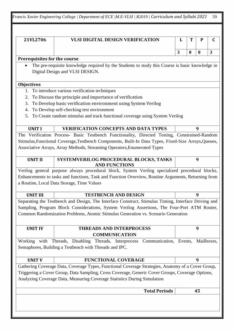
Francis Xavier Engineering College | Department of ECE |M.E-VLSI | R2019 | Curriculum and Syllabi 2021 59
21VL2706 VLSI DIGITAL DESIGN VERIFICATION L T P C
3 0 0 3
Prerequisites for the course
The pre-requisite knowledge required by the Students to study this Course is basic knowledge in
Digital Design and VLSI DESIGN.
Objectives
1. To introduce various verification techniques
2. To Discuss the principle and importance of verification
3. To Develop basic verification environment using System Verilog
4. To Develop self-checking test environment
5. To Create random stimulus and track functional coverage using System Verilog
UNIT I VERIFICATION CONCEPTS AND DATA TYPES 9
The Verification Process- Basic Testbench Functionality, Directed Testing, Constrained-Random
Stimulus,Functional Coverage,Testbench Components, Built-In Data Types, Fixed-Size Arrays,Queues,
Associative Arrays, Array Methods, Streaming Operators,Enumerated Types
UNIT II SYSTEMVERILOG PROCEDURAL BLOCKS, TASKS
AND FUNCTIONS 9
Verilog general purpose always procedural block, System Verilog specialized procedural blocks,
Enhancements to tasks and functions, Task and Function Overview, Routine Arguments, Returning from
a Routine, Local Data Storage, Time Values
UNIT III TESTBENCH AND DESIGN 9
Separating the Testbench and Design, The Interface Construct, Stimulus Timing, Interface Driving and
Sampling, Program Block Considerations, System Verilog Assertions, The Four-Port ATM Router,
Common Randomization Problems, Atomic Stimulus Generation vs. Scenario Generation
UNIT IV THREADS AND INTERPROCESS
COMMUNICATION
9
Working with Threads, Disabling Threads, Interprocess Communication, Events, Mailboxes,
Semaphores, Building a Testbench with Threads and IPC.
UNIT V FUNCTIONAL COVERAGE 9
Gathering Coverage Data, Coverage Types, Functional Coverage Strategies, Anatomy of a Cover Group,
Triggering a Cover Group, Data Sampling, Cross Coverage, Generic Cover Groups, Coverage Options,
Analyzing Coverage Data, Measuring Coverage Statistics During Simulation
Total Periods 45
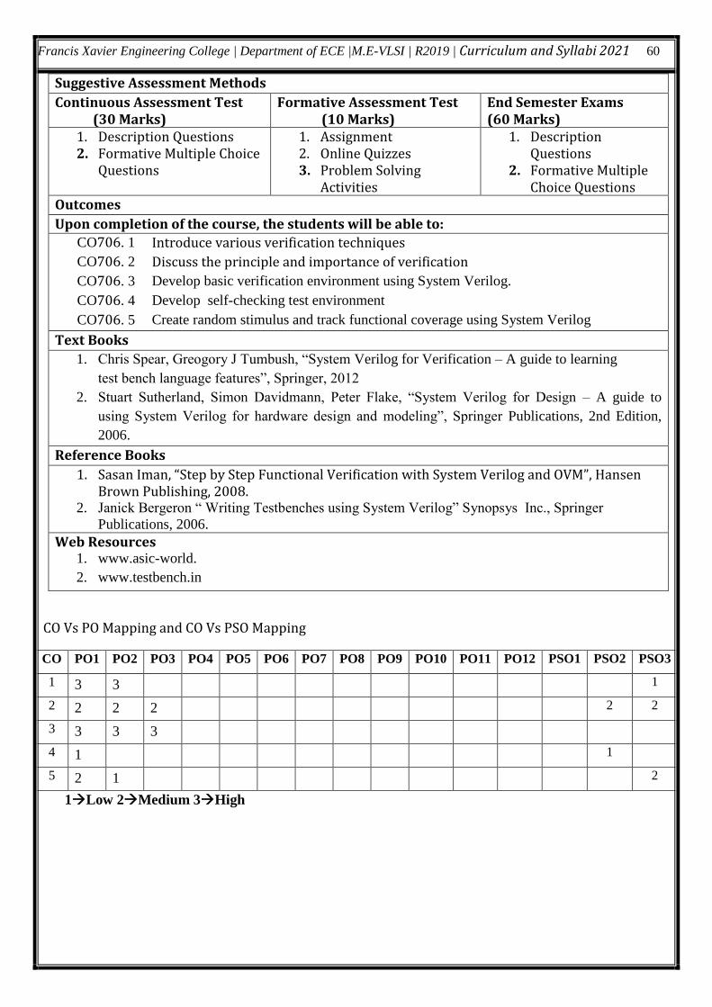
Francis Xavier Engineering College | Department of ECE |M.E-VLSI | R2019 | Curriculum and Syllabi 2021 60
Suggestive Assessment Methods
Continuous Assessment Test (30 Marks)
Formative Assessment Test (10 Marks)
End Semester Exams (60 Marks)
1. Description Questions 2. Formative Multiple Choice
Questions
1. Assignment 2. Online Quizzes 3. Problem Solving
Activities
1. Description Questions
2. Formative Multiple Choice Questions
Outcomes
Upon completion of the course, the students will be able to:
CO706. 1 Introduce various verification techniques
CO706. 2 Discuss the principle and importance of verification
CO706. 3 Develop basic verification environment using System Verilog.
CO706. 4 Develop self-checking test environment
CO706. 5 Create random stimulus and track functional coverage using System Verilog
Text Books
1. Chris Spear, Greogory J Tumbush, “System Verilog for Verification – A guide to learning
test bench language features”, Springer, 2012
2. Stuart Sutherland, Simon Davidmann, Peter Flake, “System Verilog for Design – A guide to
using System Verilog for hardware design and modeling”, Springer Publications, 2nd Edition,
2006.
Reference Books
1. Sasan Iman, “Step by Step Functional Verification with System Verilog and OVM”, Hansen Brown Publishing, 2008.
2. Janick Bergeron “ Writing Testbenches using System Verilog” Synopsys Inc., Springer
Publications, 2006.
Web Resources 1. www.asic-world.
2. www.testbench.in
CO Vs PO Mapping and CO Vs PSO Mapping
1Low 2Medium 3High
CO PO1 PO2 PO3 PO4 PO5 PO6 PO7 PO8 PO9 PO10 PO11 PO12 PSO1 PSO2 PSO3
1 3 3 1
2 2 2 2 2 2
3 3 3 3
4 1 1
5 2 1 2
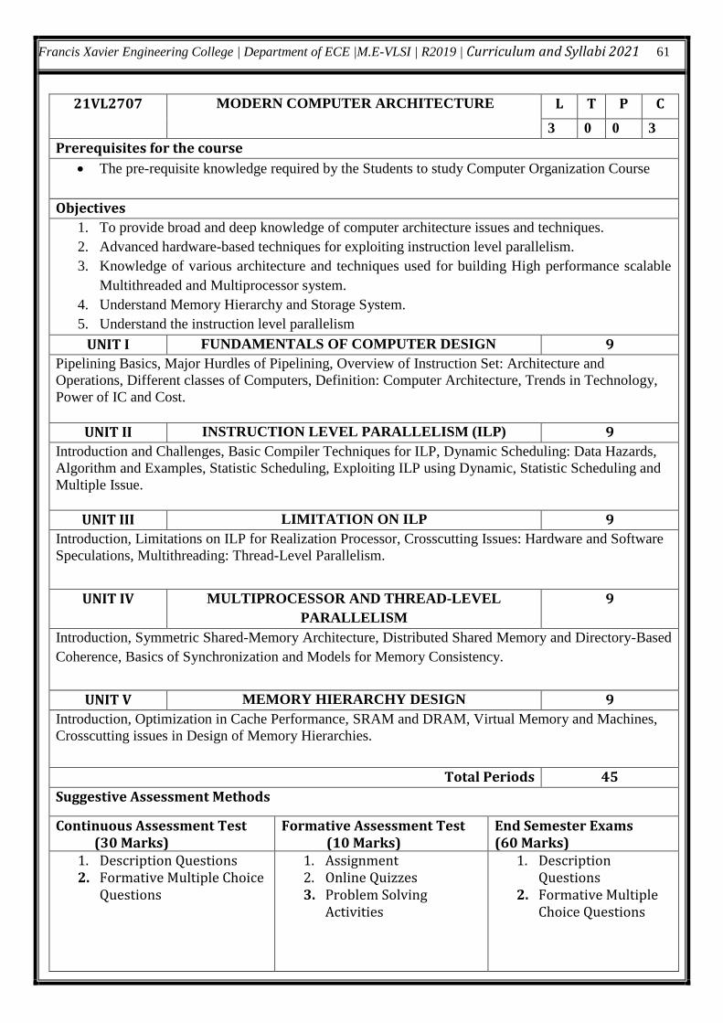
Francis Xavier Engineering College | Department of ECE |M.E-VLSI | R2019 | Curriculum and Syllabi 2021 61
21VL2707 MODERN COMPUTER ARCHITECTURE L T P C
3 0 0 3
Prerequisites for the course
The pre-requisite knowledge required by the Students to study Computer Organization Course
Objectives
1. To provide broad and deep knowledge of computer architecture issues and techniques.
2. Advanced hardware-based techniques for exploiting instruction level parallelism.
3. Knowledge of various architecture and techniques used for building High performance scalable
Multithreaded and Multiprocessor system.
4. Understand Memory Hierarchy and Storage System.
5. Understand the instruction level parallelism
UNIT I FUNDAMENTALS OF COMPUTER DESIGN 9
Pipelining Basics, Major Hurdles of Pipelining, Overview of Instruction Set: Architecture and
Operations, Different classes of Computers, Definition: Computer Architecture, Trends in Technology,
Power of IC and Cost.
UNIT II INSTRUCTION LEVEL PARALLELISM (ILP) 9
Introduction and Challenges, Basic Compiler Techniques for ILP, Dynamic Scheduling: Data Hazards,
Algorithm and Examples, Statistic Scheduling, Exploiting ILP using Dynamic, Statistic Scheduling and
Multiple Issue.
UNIT III LIMITATION ON ILP 9
Introduction, Limitations on ILP for Realization Processor, Crosscutting Issues: Hardware and Software
Speculations, Multithreading: Thread-Level Parallelism.
UNIT IV MULTIPROCESSOR AND THREAD-LEVEL
PARALLELISM
9
Introduction, Symmetric Shared-Memory Architecture, Distributed Shared Memory and Directory-Based
Coherence, Basics of Synchronization and Models for Memory Consistency.
UNIT V MEMORY HIERARCHY DESIGN 9
Introduction, Optimization in Cache Performance, SRAM and DRAM, Virtual Memory and Machines,
Crosscutting issues in Design of Memory Hierarchies.
Total Periods 45
Suggestive Assessment Methods
Continuous Assessment Test (30 Marks)
Formative Assessment Test (10 Marks)
End Semester Exams (60 Marks)
1. Description Questions 2. Formative Multiple Choice
Questions
1. Assignment 2. Online Quizzes 3. Problem Solving
Activities
1. Description Questions
2. Formative Multiple Choice Questions
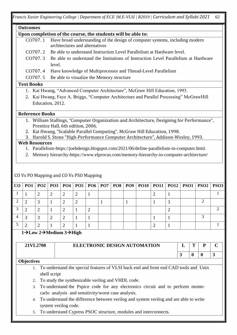
Francis Xavier Engineering College | Department of ECE |M.E-VLSI | R2019 | Curriculum and Syllabi 2021 62
Outcomes
Upon completion of the course, the students will be able to:
CO707. 1 Have broad understanding of the design of computer systems, including modern
architectures and alternatives
CO707. 2 Be able to understand Instruction Level Parallelism at Hardware level.
CO707. 3 Be able to understand the limitations of Instruction Level Parallelism at Hardware
level.
CO707. 4 Have knowledge of Multiprocessor and Thread-Level Parallelism
CO707. 5 Be able to visualize the Memory structure
Text Books
1. Kai Hwang, “Advanced Computer Architecture”, McGraw Hill Education, 1993.
2. Kai Hwang, Faye A. Briggs, “Computer Architecture and Parallel Processing” McGrawHill
Education, 2012.
Reference Books
1. William Stallings, “Computer Organization and Architecture, Designing for Performance”, Prentice Hall, 6th edition, 2006.
2. Kai Hwang, “Scalable Parallel Computing”, McGraw Hill Education, 1998. 3. Harold S. Stone “High-Performance Computer Architecture”, Addison-Wesley, 1993.
Web Resources 1. Parallelism-https://joehdesign.blogspot.com/2021/06/define-parallelism-in-computer.html.
2. Memory hierarchy-https://www.elprocus.com/memory-hierarchy-in-computer-architecture/
CO Vs PO Mapping and CO Vs PSO Mapping
1Low 2Medium 3High
21VL2708 ELECTRONIC DESIGN AUTOMATION L T P C
3 0 0 3
Objectives
1. To understand the special features of VLSI back end and front end CAD tools and Unix
shell script
2. To study the synthesizable verilog and VHDL code.
3. To understand the Pspice code for any electronics circuit and to perform monte-
carlo analysis and sensitivity/worst case analysis.
4. To understand the difference between verilog and system verilog and are able to write
system verilog code.
5. To understand Cypress PSOC structure, modules and interconnects.
CO PO1 PO2 PO3 PO4 PO5 PO6 PO7 PO8 PO9 PO10 PO11 PO12 PSO1 PSO2 PSO3
1 1 2 2 2 2 1 2 1 1
2 2 3 1 2 2 1 1 1 3 2
3 2 2 1 2 1 2 2 2
4 3 3 2 2 1 1 1 1 3
5 2 2 1 2 1 1 2 1 1
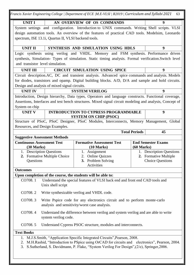
Francis Xavier Engineering College | Department of ECE |M.E-VLSI | R2019 | Curriculum and Syllabi 2021 63
UNIT I AN OVERVIEW OF OS COMMANDS 9
System settings and configuration. Introduction to UNIX commands. Writing Shell scripts. VLSI
design automation tools. An overview of the features of practical CAD tools. Modelsim, Leonardo
spectrum, ISE 13.1i, Quartus II, VLSI backend tools.
UNIT II SYNTHESIS AND SIMULATION USING HDLS 9
Logic synthesis using verilog and VHDL. Memory and FSM synthesis. Performance driven
synthesis, Simulation- Types of simulation. Static timing analysis. Formal verification.Switch level
and transistor level simulation.
UNIT III CIRCUIT SIMULATION USING SPICE 9
Circuit description.AC, DC and transient analysis. Advanced spice commands and analysis. Models
for diodes, transistors and opamp. Digital building blocks. A/D, D/A and sample and hold circuits.
Design and analysis of mixed signal circuits.
UNIT IV SYSTEM VERILOG 9
Introduction, Design hierarchy, Data types, Operators and language constructs. Functional coverage,
Assertions, Interfaces and test bench structures. Mixed signal circuit modeling and analysis, Concept of
System on chip
UNIT V INTRODUCTION TO CYPRESS PROGRAMMABLE
SYSTEM ON CHIP (PSOC)
9
Structure of PSoC, PSoC Designer, PSoC Modules, Interconnects, Memory Management, Global
Resources, and Design Examples.
Total Periods 45
Suggestive Assessment Methods
Continuous Assessment Test
(30 Marks)
Formative Assessment Test
(10 Marks)
End Semester Exams
(60 Marks)
1. Description Questions
2. Formative Multiple Choice
Questions
1. Assignment
2. Online Quizzes
3. Problem Solving
Activities
1. Description Questions
2. Formative Multiple
Choice Questions
Outcomes
Upon completion of the course, the students will be able to:
CO708. 1 Understand the special features of VLSI back end and front end CAD tools and
Unix shell script
CO708. 2 Write synthesizable verilog and VHDL code.
CO708. 3 Write Pspice code for any electronics circuit and to perform monte-carlo
analysis and sensitivity/worst case analysis.
CO708. 4 Understand the difference between verilog and system verilog and are able to write
system verilog code.
CO708. 5 Understand Cypress PSOC structure, modules and interconnects.
Text Books
1. M.J.S.Smith, “Application Specific Integrated Circuits”,Pearson, 2008.
2. M.H.Rashid, “Introduction to PSpice using OrCAD for circuits and electronics”, Pearson, 2004.
3. S.Sutherland, S. Davidmann, P. Flake, “System Verilog For Design”,(2/e), Springer,2006.
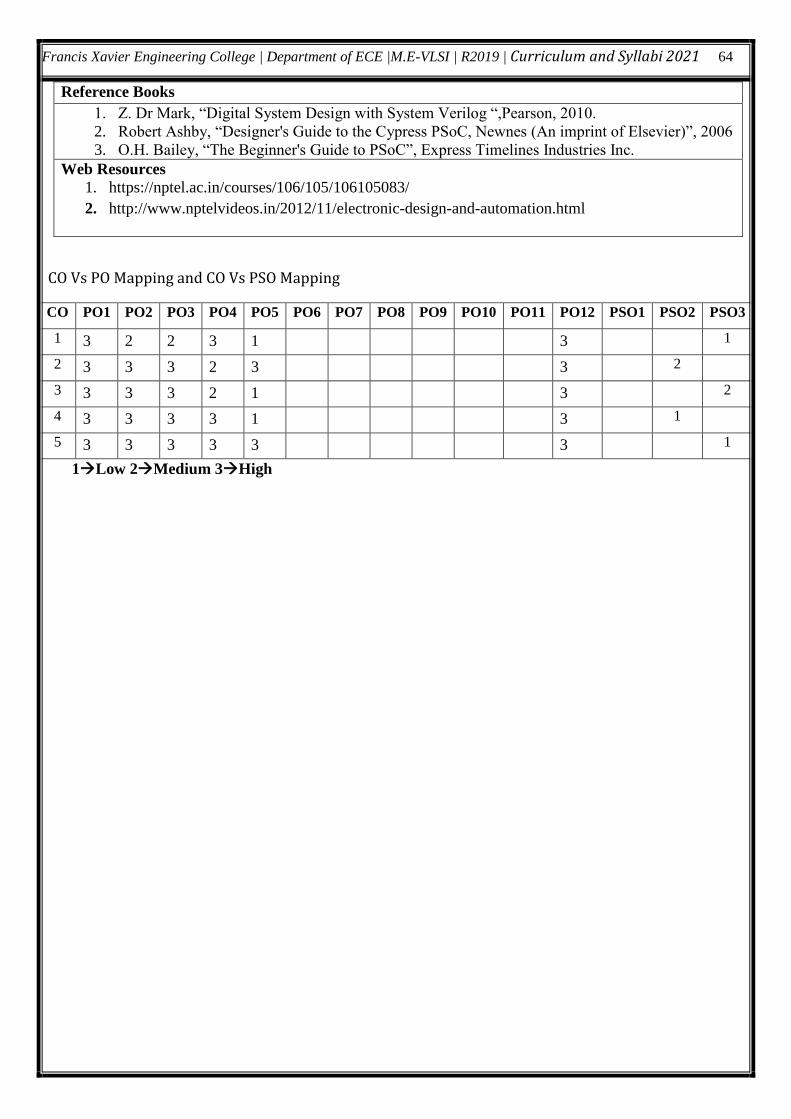
Francis Xavier Engineering College | Department of ECE |M.E-VLSI | R2019 | Curriculum and Syllabi 2021 64
Reference Books
1. Z. Dr Mark, “Digital System Design with System Verilog “,Pearson, 2010.
2. Robert Ashby, “Designer's Guide to the Cypress PSoC, Newnes (An imprint of Elsevier)”, 2006
3. O.H. Bailey, “The Beginner's Guide to PSoC”, Express Timelines Industries Inc.
Web Resources
1. https://nptel.ac.in/courses/106/105/106105083/
2. http://www.nptelvideos.in/2012/11/electronic-design-and-automation.html
CO Vs PO Mapping and CO Vs PSO Mapping
1Low 2Medium 3High
CO PO1 PO2 PO3 PO4 PO5 PO6 PO7 PO8 PO9 PO10 PO11 PO12 PSO1 PSO2 PSO3
1 3 2 2 3 1 3 1
2 3 3 3 2 3 3 2
3 3 3 3 2 1 3 2
4 3 3 3 3 1 3 1
5 3 3 3 3 3 3 1
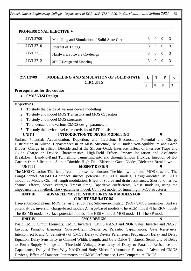
Francis Xavier Engineering College | Department of ECE |M.E-VLSI | R2019 | Curriculum and Syllabi 2021 65
PROFESSIONAL ELECTIVE V
21VL2709 Modelling and Simulation of Solid-State Circuits 3 0 0 3
21VL2710 Internet of Things 3 0 0 3
21VL2711 Hardware/Software Co-design 3 0 0 3
21VL2712 3D IC Design and Modeling 3 0 0 3
21VL2709 MODELLING AND SIMULATION OF SOLID-STATE
CIRCUITS
L T P C
3 0 0 3
Prerequisites for the course
CMOS VLSI Design
Objectives
1. To study the basics of various device modelling
2. To study and model MOS Transistors and MOS Capacitors
3. To study and model MOS structures
4. To understand the various CMOS design parameters
5. To study the device level characteristics of BJT transistors UNIT I INTRODUCTION TO DEVICE MODELLING 9
Surface Potential: Accumulation, Depletion, and Inversion, Electrostatic Potential and Charge
Distribution in Silicon, Capacitances in an MOS Structure, MOS under Non-equilibrium and Gated
Diodes, Charge in Silicon Dioxide and at the Silicon–Oxide Interface, Effect of Interface Traps and
Oxide Charge on Device Characteristics, High-Field Effects, Impact Ionization and Avalanche
Breakdown, Band-to-Band Tunnelling, Tunnelling into and through Silicon Dioxide, Injection of Hot
Carriers from Silicon into Silicon Dioxide, High-Field Effects in Gated Diodes, Dielectric Breakdown
UNIT II MOSFET DESIGN 9
The MOS Capacitor-The field effect in bulk semiconductors-The ideal two-terminal MOS structure, The
Long-Channel MOSFET-Compact surface potential MOSFET models, Design-oriented MOSFET
model, dc Models-Channel length modulation, Effect of source and drain resistances, Short and narrow
channel effects, Stored charges, Transit time, Capacitive coefficients, Noise modeling using the
impedance field method, The y-parameter model, Compact model for tunneling in MOS structures
UNIT III ADVANCED MOSFET STRUCTURES AND MODELS FOR CIRCUIT SIMULATORS
9
Deep submicron planar MOS transistor structures, Silicon-on-insulator (SOI) CMOS transistors, Surface
potential- vs. inversion charge-based models ,Charge-based models -The ACM model -The EKV model-
The BSIM5 model , Surface potential models -The HiSIM model-MOS model 11 -The SP model
UNIT IV CMOS DESIGN 9
Basic CMOS Circuit Elements, CMOS Inverters, CMOS NAND and NOR Gates, Inverter and NAND
Layouts, Parasitic Elements, Source–Drain Resistance, Parasitic Capacitances, Gate Resistance,
Interconnect R and C, Sensitivity of CMOS Delay to Device Parameters, Propagation Delay and Delay
Equation, Delay Sensitivity to Channel Width, Length, and Gate Oxide Thickness, Sensitivity of Delay
to Power-Supply Voltage and Threshold Voltage, Sensitivity of Delay to Parasitic Resistance and
Capacitance, Delay of Two-Way NAND and Body Effect, Performance Factors of Advanced CMOS
Devices, Effect of Transport Parameters on CMOS Performance, Low Temperature CMOS
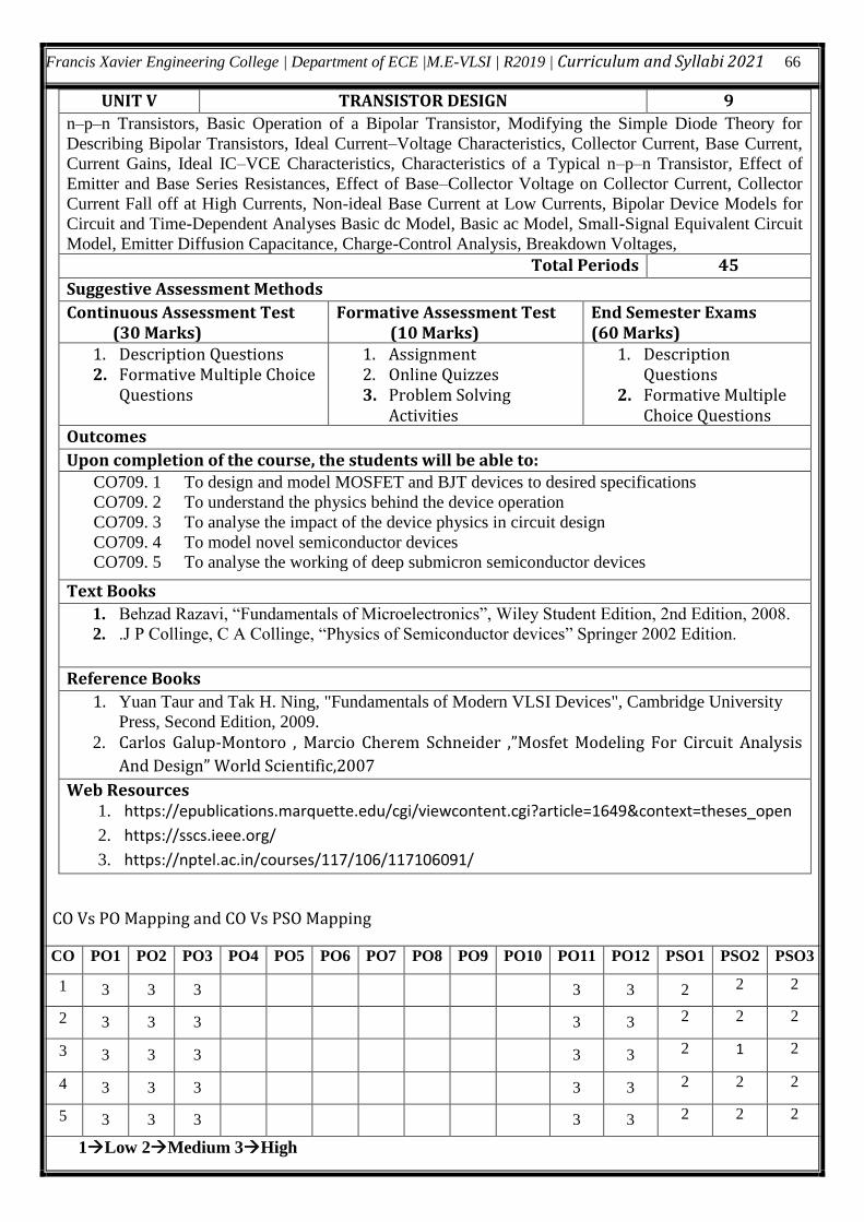
Francis Xavier Engineering College | Department of ECE |M.E-VLSI | R2019 | Curriculum and Syllabi 2021 66
UNIT V TRANSISTOR DESIGN 9
n–p–n Transistors, Basic Operation of a Bipolar Transistor, Modifying the Simple Diode Theory for
Describing Bipolar Transistors, Ideal Current–Voltage Characteristics, Collector Current, Base Current,
Current Gains, Ideal IC–VCE Characteristics, Characteristics of a Typical n–p–n Transistor, Effect of
Emitter and Base Series Resistances, Effect of Base–Collector Voltage on Collector Current, Collector
Current Fall off at High Currents, Non-ideal Base Current at Low Currents, Bipolar Device Models for
Circuit and Time-Dependent Analyses Basic dc Model, Basic ac Model, Small-Signal Equivalent Circuit
Model, Emitter Diffusion Capacitance, Charge-Control Analysis, Breakdown Voltages,
Total Periods 45
Suggestive Assessment Methods
Continuous Assessment Test (30 Marks)
Formative Assessment Test (10 Marks)
End Semester Exams (60 Marks)
1. Description Questions 2. Formative Multiple Choice
Questions
1. Assignment 2. Online Quizzes 3. Problem Solving
Activities
1. Description Questions
2. Formative Multiple Choice Questions
Outcomes
Upon completion of the course, the students will be able to: CO709. 1 To design and model MOSFET and BJT devices to desired specifications
CO709. 2 To understand the physics behind the device operation
CO709. 3 To analyse the impact of the device physics in circuit design
CO709. 4 To model novel semiconductor devices
CO709. 5 To analyse the working of deep submicron semiconductor devices
Text Books
1. Behzad Razavi, “Fundamentals of Microelectronics”, Wiley Student Edition, 2nd Edition, 2008.
2. .J P Collinge, C A Collinge, “Physics of Semiconductor devices” Springer 2002 Edition.
Reference Books
1. Yuan Taur and Tak H. Ning, "Fundamentals of Modern VLSI Devices", Cambridge University
Press, Second Edition, 2009. 2. Carlos Galup-Montoro , Marcio Cherem Schneider ,”Mosfet Modeling For Circuit Analysis
And Design” World Scientific,2007
Web Resources 1. https://epublications.marquette.edu/cgi/viewcontent.cgi?article=1649&context=theses_open
2. https://sscs.ieee.org/
3. https://nptel.ac.in/courses/117/106/117106091/
CO Vs PO Mapping and CO Vs PSO Mapping
1Low 2Medium 3High
CO PO1 PO2 PO3 PO4 PO5 PO6 PO7 PO8 PO9 PO10 PO11 PO12 PSO1 PSO2 PSO3
1 3 3 3 3 3 2 2 2
2 3 3 3 3 3 2 2 2
3 3 3 3 3 3 2 1 2
4 3 3 3 3 3 2 2 2
5 3 3 3 3 3 2 2 2
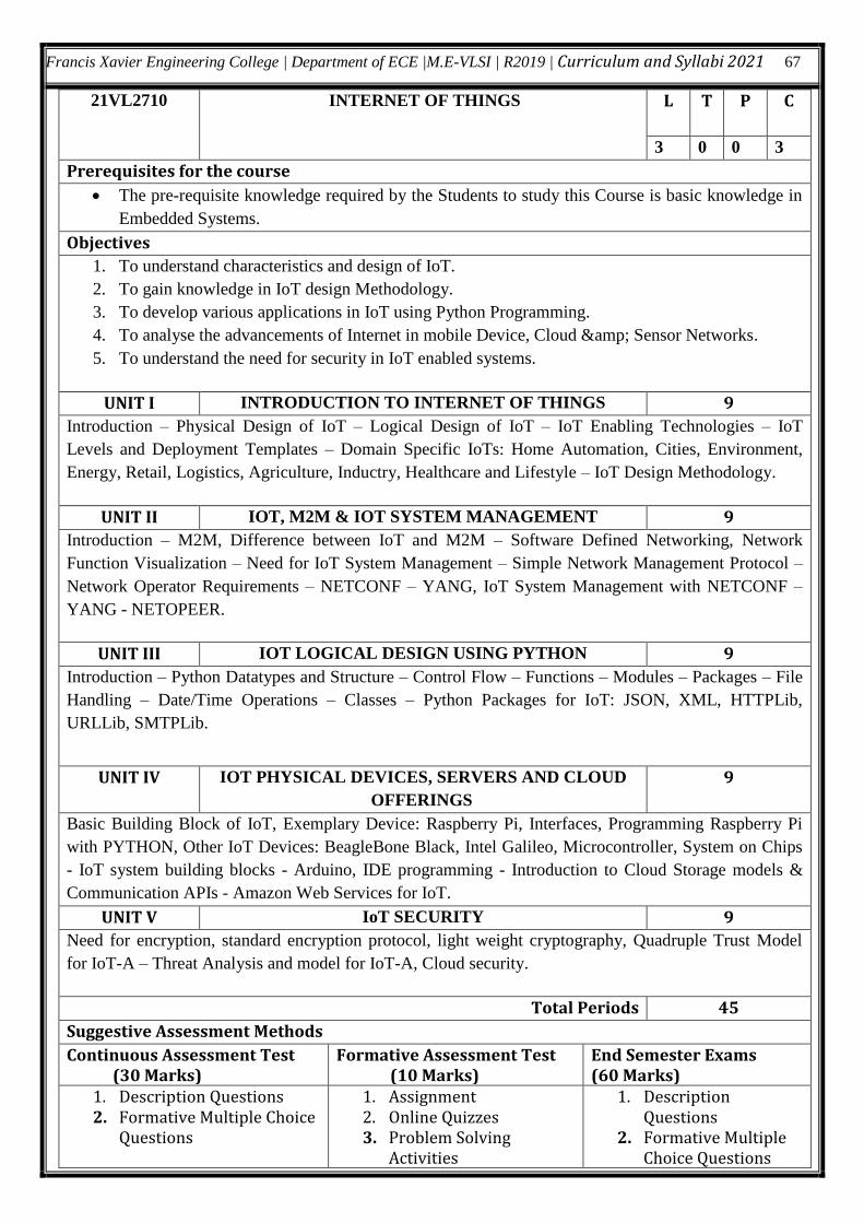
Francis Xavier Engineering College | Department of ECE |M.E-VLSI | R2019 | Curriculum and Syllabi 2021 67
21VL2710 INTERNET OF THINGS L T P C
3 0 0 3
Prerequisites for the course
The pre-requisite knowledge required by the Students to study this Course is basic knowledge in
Embedded Systems.
Objectives
1. To understand characteristics and design of IoT.
2. To gain knowledge in IoT design Methodology.
3. To develop various applications in IoT using Python Programming.
4. To analyse the advancements of Internet in mobile Device, Cloud & Sensor Networks.
5. To understand the need for security in IoT enabled systems.
UNIT I INTRODUCTION TO INTERNET OF THINGS 9
Introduction – Physical Design of IoT – Logical Design of IoT – IoT Enabling Technologies – IoT
Levels and Deployment Templates – Domain Specific IoTs: Home Automation, Cities, Environment,
Energy, Retail, Logistics, Agriculture, Inductry, Healthcare and Lifestyle – IoT Design Methodology.
UNIT II IOT, M2M & IOT SYSTEM MANAGEMENT 9
Introduction – M2M, Difference between IoT and M2M – Software Defined Networking, Network
Function Visualization – Need for IoT System Management – Simple Network Management Protocol –
Network Operator Requirements – NETCONF – YANG, IoT System Management with NETCONF –
YANG - NETOPEER.
UNIT III IOT LOGICAL DESIGN USING PYTHON 9
Introduction – Python Datatypes and Structure – Control Flow – Functions – Modules – Packages – File
Handling – Date/Time Operations – Classes – Python Packages for IoT: JSON, XML, HTTPLib,
URLLib, SMTPLib.
UNIT IV IOT PHYSICAL DEVICES, SERVERS AND CLOUD
OFFERINGS
9
Basic Building Block of IoT, Exemplary Device: Raspberry Pi, Interfaces, Programming Raspberry Pi
with PYTHON, Other IoT Devices: BeagleBone Black, Intel Galileo, Microcontroller, System on Chips
- IoT system building blocks - Arduino, IDE programming - Introduction to Cloud Storage models &
Communication APIs - Amazon Web Services for IoT.
UNIT V IoT SECURITY 9
Need for encryption, standard encryption protocol, light weight cryptography, Quadruple Trust Model
for IoT-A – Threat Analysis and model for IoT-A, Cloud security.
Total Periods 45
Suggestive Assessment Methods
Continuous Assessment Test (30 Marks)
Formative Assessment Test (10 Marks)
End Semester Exams (60 Marks)
1. Description Questions 2. Formative Multiple Choice
Questions
1. Assignment 2. Online Quizzes 3. Problem Solving
Activities
1. Description Questions
2. Formative Multiple Choice Questions
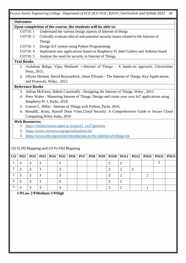
Francis Xavier Engineering College | Department of ECE |M.E-VLSI | R2019 | Curriculum and Syllabi 2021 68
Outcomes
Upon completion of the course, the students will be able to: CO710. 1 Understand the various design aspects of Internet of things
CO710. 2 Critically evaluate ethical and potential security issues related to the Internet of
Things
CO710. 3 Design IoT system using Python Programming
CO710. 4 Implement new applications based on Raspberry Pi ,Intel Galileo and Arduino board
CO710. 5 Analyse the need for security in Internet of Things
Text Books
1. Arshdeep Bahga, Vijay Madisetti ―Internet of Things – A hands-on approach, Universities
Press, 2015.
2. Olivier Hersent, David Boswarthick, Omar Elloumi - The Internet of Things: Key Applications
and Protocols, Wiley , 2012
Reference Books
3. Adrian McEwen, Hakim Cassimally - Designing the Internet of Things, Wiley , 2013
4. Peter Waher - Mastering Internet of Things: Design and create your own IoT applications using
Raspberry Pi 3, Packt, 2018.
5. Gaston C. Hillar - Internet of Things with Python, Packt, 2016.
6. RonaldL. Krutz, Russell Dean Vines,Cloud Security: A Comprehensive Guide to Secure Cloud
Computing,Wiley-India, 2010
Web Resources 1. https://onlinecourses.nptel.ac.in/noc21_cs17/preview
2. https://www.coursera.org/specializations/iot
3. https://www.edx.org/course/introduction-to-the-internet-of-things-iot
CO Vs PO Mapping and CO Vs PSO Mapping
1Low 2Medium 3High
CO PO1 PO2 PO3 PO4 PO5 PO6 PO7 PO8 PO9 PO10 PO11 PO12 PSO1 PSO2 PSO3
1 3 3 3 3 2 2 2
2 3 3 3 3 2 2 2
3 3 3 3 3 2 2 2
4 3 3 3 3 2 2
5 3 3 3 3 2 2 1
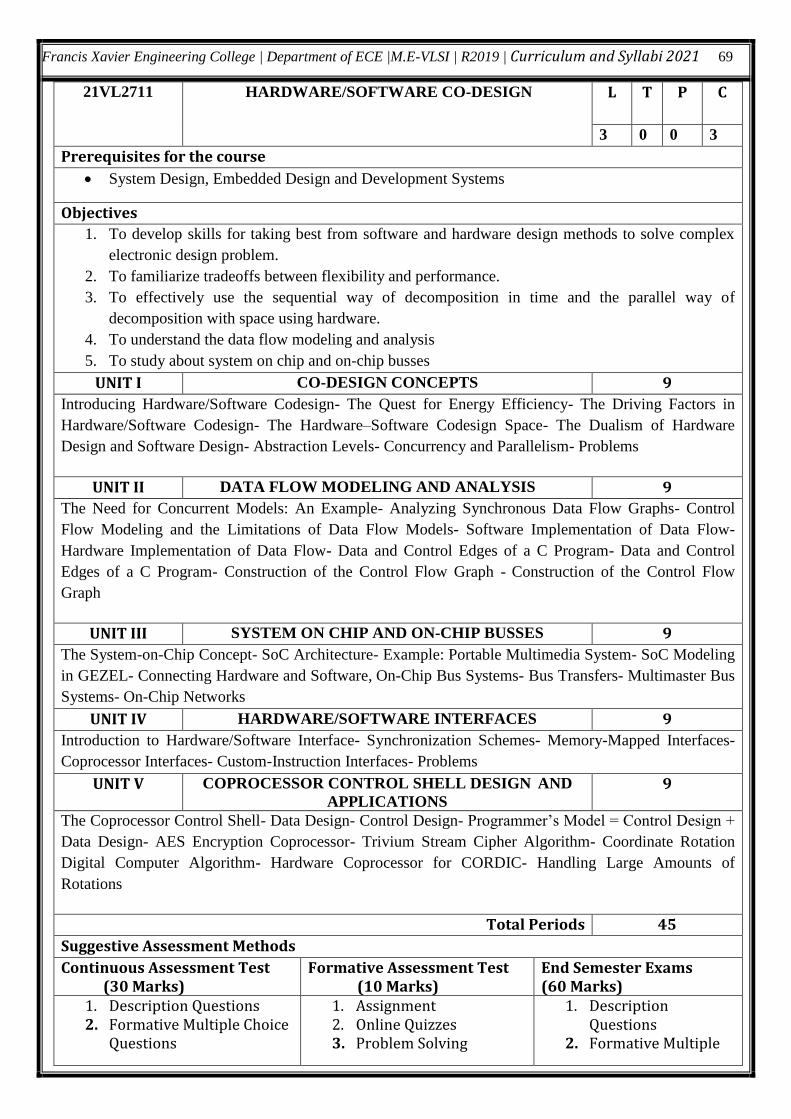
Francis Xavier Engineering College | Department of ECE |M.E-VLSI | R2019 | Curriculum and Syllabi 2021 69
21VL2711 HARDWARE/SOFTWARE CO-DESIGN L T P C
3 0 0 3
Prerequisites for the course
System Design, Embedded Design and Development Systems
Objectives
1. To develop skills for taking best from software and hardware design methods to solve complex
electronic design problem.
2. To familiarize tradeoffs between flexibility and performance.
3. To effectively use the sequential way of decomposition in time and the parallel way of
decomposition with space using hardware.
4. To understand the data flow modeling and analysis
5. To study about system on chip and on-chip busses
UNIT I CO-DESIGN CONCEPTS 9
Introducing Hardware/Software Codesign- The Quest for Energy Efficiency- The Driving Factors in
Hardware/Software Codesign- The Hardware–Software Codesign Space- The Dualism of Hardware
Design and Software Design- Abstraction Levels- Concurrency and Parallelism- Problems
UNIT II DATA FLOW MODELING AND ANALYSIS 9
The Need for Concurrent Models: An Example- Analyzing Synchronous Data Flow Graphs- Control
Flow Modeling and the Limitations of Data Flow Models- Software Implementation of Data Flow-
Hardware Implementation of Data Flow- Data and Control Edges of a C Program- Data and Control
Edges of a C Program- Construction of the Control Flow Graph - Construction of the Control Flow
Graph
UNIT III SYSTEM ON CHIP AND ON-CHIP BUSSES 9
The System-on-Chip Concept- SoC Architecture- Example: Portable Multimedia System- SoC Modeling
in GEZEL- Connecting Hardware and Software, On-Chip Bus Systems- Bus Transfers- Multimaster Bus
Systems- On-Chip Networks
UNIT IV HARDWARE/SOFTWARE INTERFACES 9
Introduction to Hardware/Software Interface- Synchronization Schemes- Memory-Mapped Interfaces-
Coprocessor Interfaces- Custom-Instruction Interfaces- Problems
UNIT V COPROCESSOR CONTROL SHELL DESIGN AND
APPLICATIONS 9
The Coprocessor Control Shell- Data Design- Control Design- Programmer’s Model = Control Design +
Data Design- AES Encryption Coprocessor- Trivium Stream Cipher Algorithm- Coordinate Rotation
Digital Computer Algorithm- Hardware Coprocessor for CORDIC- Handling Large Amounts of
Rotations
Total Periods 45
Suggestive Assessment Methods
Continuous Assessment Test (30 Marks)
Formative Assessment Test (10 Marks)
End Semester Exams (60 Marks)
1. Description Questions 2. Formative Multiple Choice
Questions
1. Assignment 2. Online Quizzes 3. Problem Solving
1. Description Questions
2. Formative Multiple
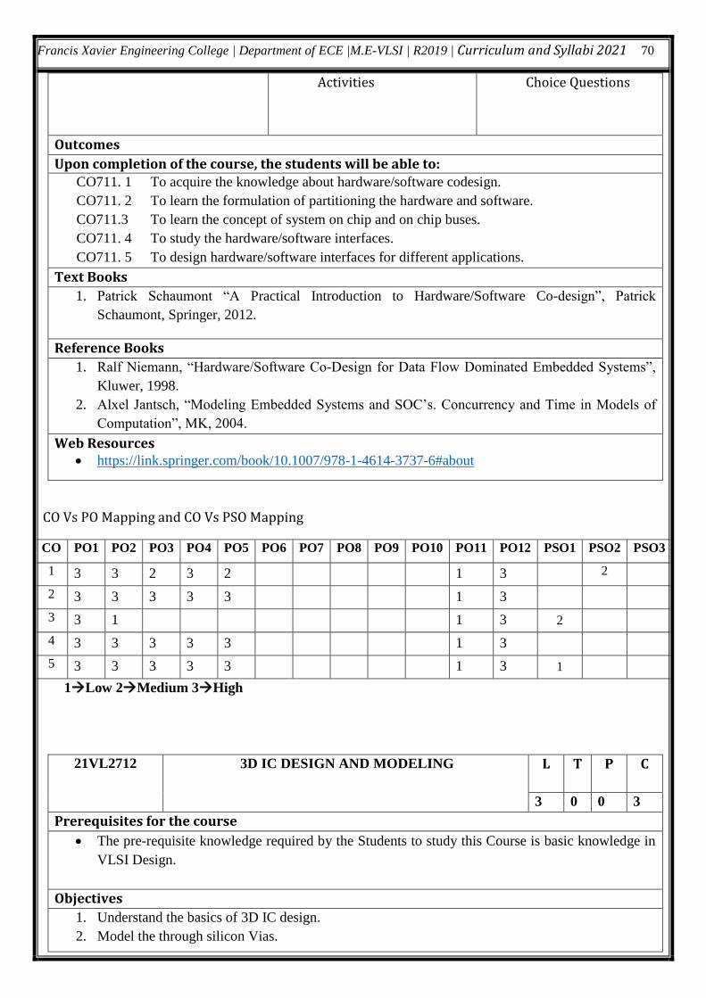
Francis Xavier Engineering College | Department of ECE |M.E-VLSI | R2019 | Curriculum and Syllabi 2021 70
Activities Choice Questions
Outcomes
Upon completion of the course, the students will be able to: CO711. 1 To acquire the knowledge about hardware/software codesign.
CO711. 2 To learn the formulation of partitioning the hardware and software.
CO711.3 To learn the concept of system on chip and on chip buses.
CO711. 4 To study the hardware/software interfaces.
CO711. 5 To design hardware/software interfaces for different applications.
Text Books
1. Patrick Schaumont “A Practical Introduction to Hardware/Software Co-design”, Patrick
Schaumont, Springer, 2012.
Reference Books
1. Ralf Niemann, “Hardware/Software Co-Design for Data Flow Dominated Embedded Systems”,
Kluwer, 1998.
2. Alxel Jantsch, “Modeling Embedded Systems and SOC’s. Concurrency and Time in Models of
Computation”, MK, 2004.
Web Resources https://link.springer.com/book/10.1007/978-1-4614-3737-6#about
CO Vs PO Mapping and CO Vs PSO Mapping
1Low 2Medium 3High
21VL2712 3D IC DESIGN AND MODELING L T P C
3 0 0 3
Prerequisites for the course
The pre-requisite knowledge required by the Students to study this Course is basic knowledge in
VLSI Design.
Objectives
1. Understand the basics of 3D IC design.
2. Model the through silicon Vias.
CO PO1 PO2 PO3 PO4 PO5 PO6 PO7 PO8 PO9 PO10 PO11 PO12 PSO1 PSO2 PSO3
1 3 3 2 3 2 1 3 2
2 3 3 3 3 3 1 3
3 3 1 1 3 2
4 3 3 3 3 3 1 3
5 3 3 3 3 3 1 3 1
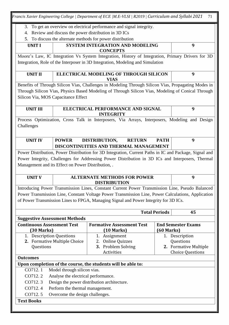
Francis Xavier Engineering College | Department of ECE |M.E-VLSI | R2019 | Curriculum and Syllabi 2021 71
3. To get an overview on electrical performance and signal integrity.
4. Review and discuss the power distribution in 3D ICs
5. To discuss the alternate methods for power distribution
UNIT I SYSTEM INTEGRATION AND MODELING
CONCEPTS 9
Moore’s Law, IC Integration Vs System Integration, History of Integration, Primary Drivers for 3D
Integration, Role of the Interposer in 3D Integration, Modeling and Simulation
UNIT II ELECTRICAL MODELING OF THROUGH SILICON
VIAS 9
Benefits of Through Silicon Vias, Challenges in Modeling Through Silicon Vias, Propagating Modes in
Through Silicon Vias, Physics Based Modeling of Through Silicon Vias, Modeling of Conical Through
Silicon Via, MOS Capacitance Effect
UNIT III ELECTRICAL PERFORMANCE AND SIGNAL
INTEGRITY 9
Process Optimization, Cross Talk in Interposers, Via Arrays, Interposers, Modeling and Design
Challenges
UNIT IV POWER DISTRIBUTION, RETURN PATH
DISCONTINUITIES AND THERMAL MANAGEMENT
9
Power Distribution, Power Distribution for 3D Integration, Current Paths in IC and Package, Signal and
Power Integrity, Challenges for Addressing Power Distribution in 3D ICs and Interposers, Thermal
Management and its Effect on Power Distribution, .
UNIT V ALTERNATE METHODS FOR POWER
DISTRIBUTION 9
Introducing Power Transmission Lines, Constant Current Power Transmission Line, Pseudo Balanced
Power Transmission Line, Constant Voltage Power Transmission Line, Power Calculations, Application
of Power Transmission Lines to FPGA, Managing Signal and Power Integrity for 3D ICs.
Total Periods 45
Suggestive Assessment Methods
Continuous Assessment Test (30 Marks)
Formative Assessment Test (10 Marks)
End Semester Exams (60 Marks)
1. Description Questions 2. Formative Multiple Choice
Questions
1. Assignment 2. Online Quizzes 3. Problem Solving
Activities
1. Description Questions
2. Formative Multiple Choice Questions
Outcomes
Upon completion of the course, the students will be able to: CO712. 1 Model through silicon vias.
CO712. 2 Analyse the electrical performance.
CO712. 3 Design the power distribution architecture.
CO712. 4 Perform the thermal management.
CO712. 5 Overcome the design challenges.
Text Books
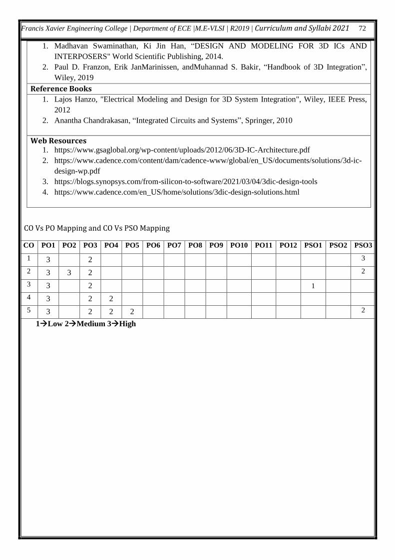
Francis Xavier Engineering College | Department of ECE |M.E-VLSI | R2019 | Curriculum and Syllabi 2021 72
1. Madhavan Swaminathan, Ki Jin Han, “DESIGN AND MODELING FOR 3D ICs AND
INTERPOSERS" World Scientific Publishing, 2014.
2. Paul D. Franzon, Erik JanMarinissen, andMuhannad S. Bakir, “Handbook of 3D Integration”,
Wiley, 2019
Reference Books
1. Lajos Hanzo, "Electrical Modeling and Design for 3D System Integration", Wiley, IEEE Press,
2012
2. Anantha Chandrakasan, “Integrated Circuits and Systems”, Springer, 2010
Web Resources 1. https://www.gsaglobal.org/wp-content/uploads/2012/06/3D-IC-Architecture.pdf
2. https://www.cadence.com/content/dam/cadence-www/global/en_US/documents/solutions/3d-ic-
design-wp.pdf
3. https://blogs.synopsys.com/from-silicon-to-software/2021/03/04/3dic-design-tools
4. https://www.cadence.com/en_US/home/solutions/3dic-design-solutions.html
CO Vs PO Mapping and CO Vs PSO Mapping
1Low 2Medium 3High
CO PO1 PO2 PO3 PO4 PO5 PO6 PO7 PO8 PO9 PO10 PO11 PO12 PSO1 PSO2 PSO3
1 3 2 3
2 3 3 2 2
3 3 2 1
4 3 2 2
5 3 2 2 2 2
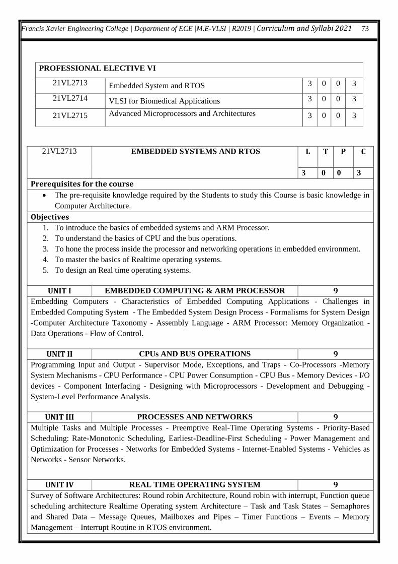
Francis Xavier Engineering College | Department of ECE |M.E-VLSI | R2019 | Curriculum and Syllabi 2021 73
PROFESSIONAL ELECTIVE VI
21VL2713 Embedded System and RTOS 3 0 0 3
21VL2714 VLSI for Biomedical Applications 3 0 0 3
21VL2715 Advanced Microprocessors and Architectures
3 0 0 3
21VL2713 EMBEDDED SYSTEMS AND RTOS L T P C
3 0 0 3
Prerequisites for the course
The pre-requisite knowledge required by the Students to study this Course is basic knowledge in
Computer Architecture.
Objectives
1. To introduce the basics of embedded systems and ARM Processor.
2. To understand the basics of CPU and the bus operations.
3. To hone the process inside the processor and networking operations in embedded environment.
4. To master the basics of Realtime operating systems.
5. To design an Real time operating systems.
UNIT I EMBEDDED COMPUTING & ARM PROCESSOR 9
Embedding Computers - Characteristics of Embedded Computing Applications - Challenges in
Embedded Computing System - The Embedded System Design Process - Formalisms for System Design
-Computer Architecture Taxonomy - Assembly Language - ARM Processor: Memory Organization -
Data Operations - Flow of Control.
UNIT II CPUs AND BUS OPERATIONS 9
Programming Input and Output - Supervisor Mode, Exceptions, and Traps - Co-Processors -Memory
System Mechanisms - CPU Performance - CPU Power Consumption - CPU Bus - Memory Devices - I/O
devices - Component Interfacing - Designing with Microprocessors - Development and Debugging -
System-Level Performance Analysis.
UNIT III PROCESSES AND NETWORKS 9
Multiple Tasks and Multiple Processes - Preemptive Real-Time Operating Systems - Priority-Based
Scheduling: Rate-Monotonic Scheduling, Earliest-Deadline-First Scheduling - Power Management and
Optimization for Processes - Networks for Embedded Systems - Internet-Enabled Systems - Vehicles as
Networks - Sensor Networks.
UNIT IV REAL TIME OPERATING SYSTEM 9
Survey of Software Architectures: Round robin Architecture, Round robin with interrupt, Function queue
scheduling architecture Realtime Operating system Architecture – Task and Task States – Semaphores
and Shared Data – Message Queues, Mailboxes and Pipes – Timer Functions – Events – Memory
Management – Interrupt Routine in RTOS environment.
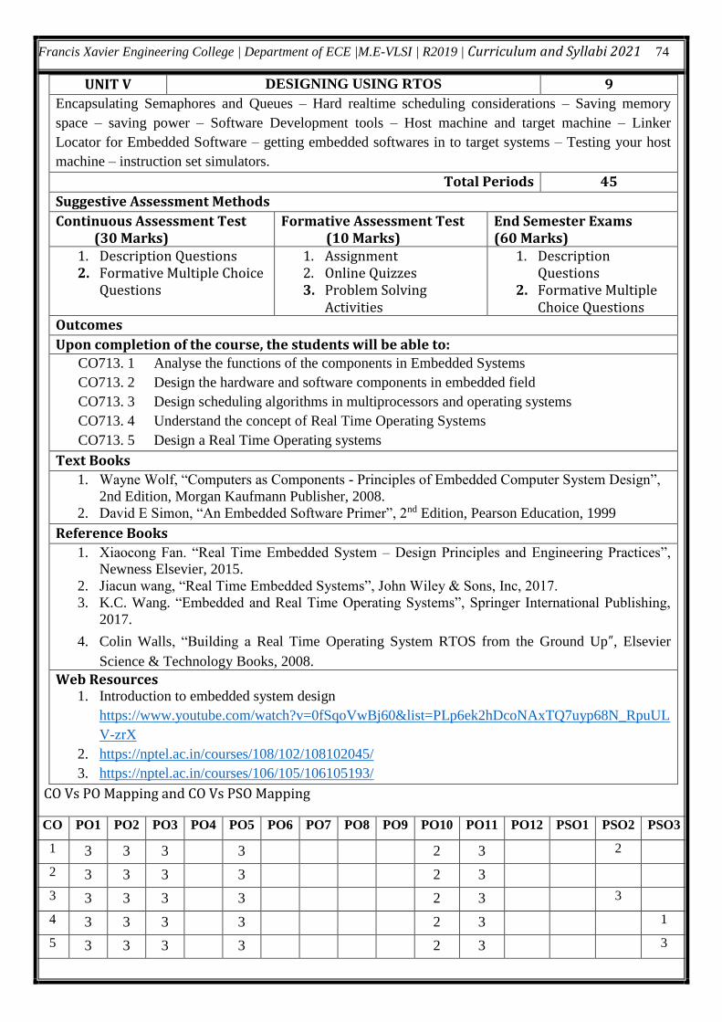
Francis Xavier Engineering College | Department of ECE |M.E-VLSI | R2019 | Curriculum and Syllabi 2021 74
UNIT V DESIGNING USING RTOS 9
Encapsulating Semaphores and Queues – Hard realtime scheduling considerations – Saving memory
space – saving power – Software Development tools – Host machine and target machine – Linker
Locator for Embedded Software – getting embedded softwares in to target systems – Testing your host
machine – instruction set simulators.
Total Periods 45
Suggestive Assessment Methods
Continuous Assessment Test (30 Marks)
Formative Assessment Test (10 Marks)
End Semester Exams (60 Marks)
1. Description Questions 2. Formative Multiple Choice
Questions
1. Assignment 2. Online Quizzes 3. Problem Solving
Activities
1. Description Questions
2. Formative Multiple Choice Questions
Outcomes
Upon completion of the course, the students will be able to:
CO713. 1 Analyse the functions of the components in Embedded Systems
CO713. 2 Design the hardware and software components in embedded field
CO713. 3 Design scheduling algorithms in multiprocessors and operating systems
CO713. 4 Understand the concept of Real Time Operating Systems
CO713. 5 Design a Real Time Operating systems
Text Books
1. Wayne Wolf, “Computers as Components - Principles of Embedded Computer System Design”,
2nd Edition, Morgan Kaufmann Publisher, 2008.
2. David E Simon, “An Embedded Software Primer”, 2nd Edition, Pearson Education, 1999
Reference Books
1. Xiaocong Fan. “Real Time Embedded System – Design Principles and Engineering Practices”,
Newness Elsevier, 2015.
2. Jiacun wang, “Real Time Embedded Systems”, John Wiley & Sons, Inc, 2017.
3. K.C. Wang. “Embedded and Real Time Operating Systems”, Springer International Publishing,
2017.
4. Colin Walls, “Building a Real Time Operating System RTOS from the Ground Up”, Elsevier
Science & Technology Books, 2008.
Web Resources 1. Introduction to embedded system design
https://www.youtube.com/watch?v=0fSqoVwBj60&list=PLp6ek2hDcoNAxTQ7uyp68N_RpuUL
V-zrX
2. https://nptel.ac.in/courses/108/102/108102045/
3. https://nptel.ac.in/courses/106/105/106105193/
CO Vs PO Mapping and CO Vs PSO Mapping
CO PO1 PO2 PO3 PO4 PO5 PO6 PO7 PO8 PO9 PO10 PO11 PO12 PSO1 PSO2 PSO3
1 3 3 3 3 2 3 2
2 3 3 3 3 2 3
3 3 3 3 3 2 3 3
4 3 3 3 3 2 3 1
5 3 3 3 3 2 3 3
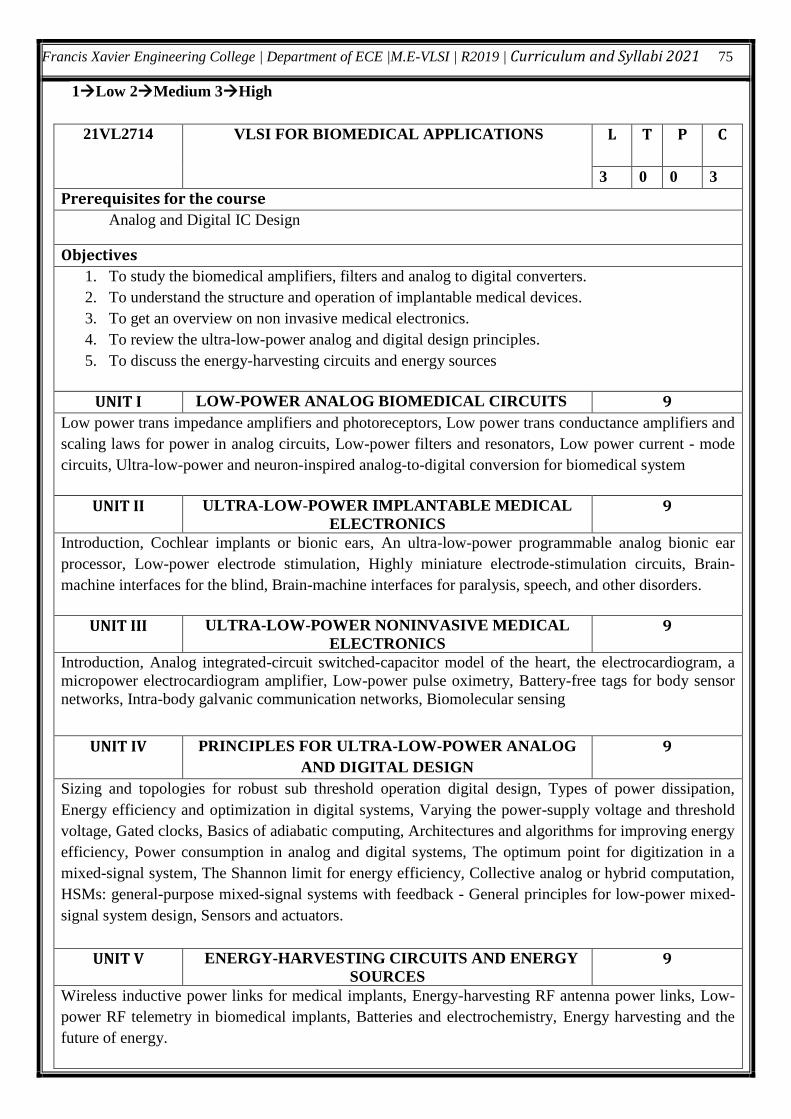
Francis Xavier Engineering College | Department of ECE |M.E-VLSI | R2019 | Curriculum and Syllabi 2021 75
1Low 2Medium 3High
21VL2714 VLSI FOR BIOMEDICAL APPLICATIONS L T P C
3 0 0 3
Prerequisites for the course
Analog and Digital IC Design
Objectives
1. To study the biomedical amplifiers, filters and analog to digital converters.
2. To understand the structure and operation of implantable medical devices.
3. To get an overview on non invasive medical electronics.
4. To review the ultra-low-power analog and digital design principles.
5. To discuss the energy-harvesting circuits and energy sources
UNIT I LOW-POWER ANALOG BIOMEDICAL CIRCUITS 9
Low power trans impedance amplifiers and photoreceptors, Low power trans conductance amplifiers and
scaling laws for power in analog circuits, Low-power filters and resonators, Low power current - mode
circuits, Ultra-low-power and neuron-inspired analog-to-digital conversion for biomedical system
UNIT II ULTRA-LOW-POWER IMPLANTABLE MEDICAL
ELECTRONICS 9
Introduction, Cochlear implants or bionic ears, An ultra-low-power programmable analog bionic ear
processor, Low-power electrode stimulation, Highly miniature electrode-stimulation circuits, Brain-
machine interfaces for the blind, Brain-machine interfaces for paralysis, speech, and other disorders.
UNIT III ULTRA-LOW-POWER NONINVASIVE MEDICAL
ELECTRONICS 9
Introduction, Analog integrated-circuit switched-capacitor model of the heart, the electrocardiogram, a
micropower electrocardiogram amplifier, Low-power pulse oximetry, Battery-free tags for body sensor
networks, Intra-body galvanic communication networks, Biomolecular sensing
UNIT IV PRINCIPLES FOR ULTRA-LOW-POWER ANALOG
AND DIGITAL DESIGN
9
Sizing and topologies for robust sub threshold operation digital design, Types of power dissipation,
Energy efficiency and optimization in digital systems, Varying the power-supply voltage and threshold
voltage, Gated clocks, Basics of adiabatic computing, Architectures and algorithms for improving energy
efficiency, Power consumption in analog and digital systems, The optimum point for digitization in a
mixed-signal system, The Shannon limit for energy efficiency, Collective analog or hybrid computation,
HSMs: general-purpose mixed-signal systems with feedback - General principles for low-power mixed-
signal system design, Sensors and actuators.
UNIT V ENERGY-HARVESTING CIRCUITS AND ENERGY
SOURCES 9
Wireless inductive power links for medical implants, Energy-harvesting RF antenna power links, Low-
power RF telemetry in biomedical implants, Batteries and electrochemistry, Energy harvesting and the
future of energy.
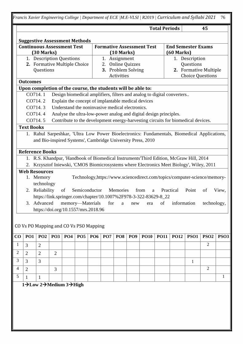
Francis Xavier Engineering College | Department of ECE |M.E-VLSI | R2019 | Curriculum and Syllabi 2021 76
Total Periods 45
Suggestive Assessment Methods Continuous Assessment Test (30 Marks)
Formative Assessment Test (10 Marks)
End Semester Exams (60 Marks)
1. Description Questions 2. Formative Multiple Choice
Questions
1. Assignment 2. Online Quizzes 3. Problem Solving
Activities
1. Description Questions
2. Formative Multiple Choice Questions
Outcomes
Upon completion of the course, the students will be able to: CO714. 1 Design biomedical amplifiers, filters and analog to digital converters..
CO714. 2 Explain the concept of implantable medical devices
CO714. 3 Understand the noninvasive medical electronics.
CO714. 4 Analyse the ultra-low-power analog and digital design principles.
CO714. 5 Contribute to the development energy-harvesting circuits for biomedical devices.
Text Books
1. Rahul Sarpeshkar, 'Ultra Low Power Bioelectronics: Fundamentals, Biomedical Applications,
and Bio-inspired Systems', Cambridge University Press, 2010
Reference Books
1. R.S. Khandpur, 'Handbook of Biomedical Instruments'Third Edition, McGraw Hill, 2014
2. Krzysztof Iniewski, 'CMOS Biomicrosystems where Electronics Meet Biology', Wiley, 2011
Web Resources 1. Memory Technology,https://www.sciencedirect.com/topics/computer-science/memory-
technology
2. Reliability of Semiconductor Memories from a Practical Point of View,
https://link.springer.com/chapter/10.1007%2F978-3-322-83629-8_22
3. Advanced memory—Materials for a new era of information technology,
https://doi.org/10.1557/mrs.2018.96
CO Vs PO Mapping and CO Vs PSO Mapping
1Low 2Medium 3High
CO PO1 PO2 PO3 PO4 PO5 PO6 PO7 PO8 PO9 PO10 PO11 PO12 PSO1 PSO2 PSO3
1 3 2 2
2 2 2 2
3 3 3 1
4 2 3 2
5 1 1 1
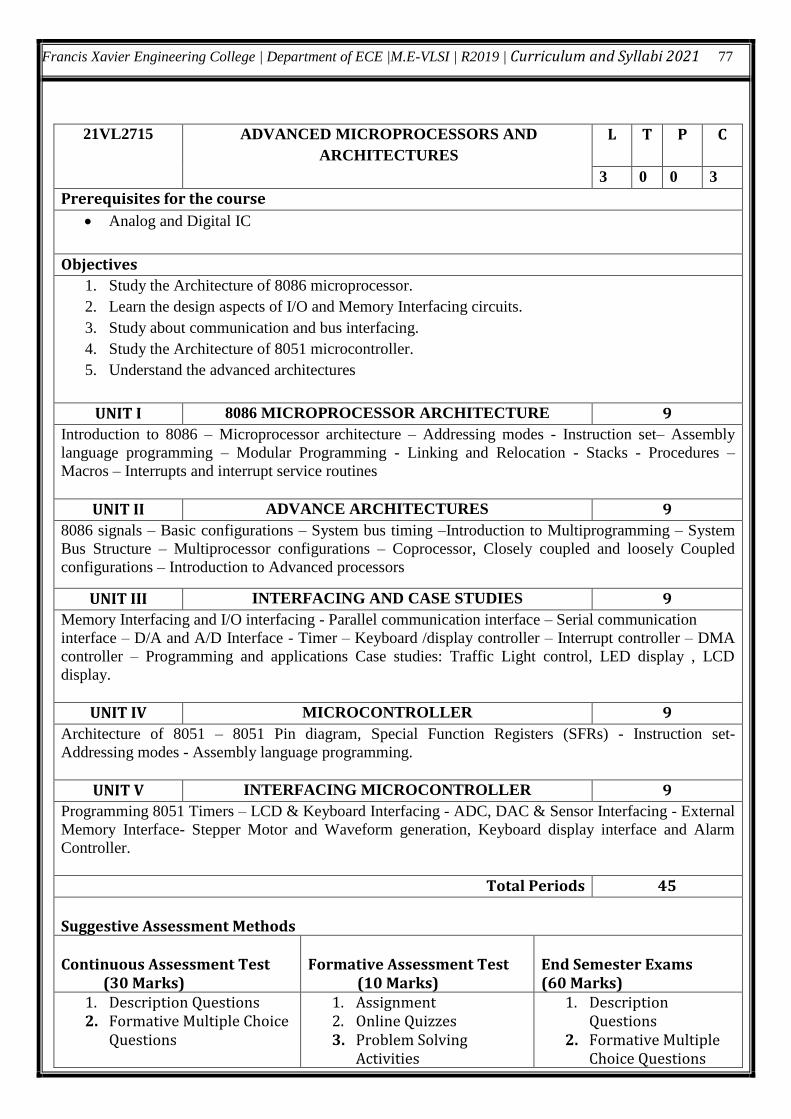
Francis Xavier Engineering College | Department of ECE |M.E-VLSI | R2019 | Curriculum and Syllabi 2021 77
21VL2715 ADVANCED MICROPROCESSORS AND
ARCHITECTURES
L T P C
3 0 0 3
Prerequisites for the course
Analog and Digital IC
Objectives
1. Study the Architecture of 8086 microprocessor.
2. Learn the design aspects of I/O and Memory Interfacing circuits.
3. Study about communication and bus interfacing.
4. Study the Architecture of 8051 microcontroller.
5. Understand the advanced architectures
UNIT I 8086 MICROPROCESSOR ARCHITECTURE 9
Introduction to 8086 – Microprocessor architecture – Addressing modes - Instruction set– Assembly
language programming – Modular Programming - Linking and Relocation - Stacks - Procedures –
Macros – Interrupts and interrupt service routines
UNIT II ADVANCE ARCHITECTURES 9
8086 signals – Basic configurations – System bus timing –Introduction to Multiprogramming – System
Bus Structure – Multiprocessor configurations – Coprocessor, Closely coupled and loosely Coupled
configurations – Introduction to Advanced processors
UNIT III INTERFACING AND CASE STUDIES 9
Memory Interfacing and I/O interfacing - Parallel communication interface – Serial communication
interface – D/A and A/D Interface - Timer – Keyboard /display controller – Interrupt controller – DMA
controller – Programming and applications Case studies: Traffic Light control, LED display , LCD
display.
UNIT IV MICROCONTROLLER 9
Architecture of 8051 – 8051 Pin diagram, Special Function Registers (SFRs) - Instruction set-
Addressing modes - Assembly language programming.
UNIT V INTERFACING MICROCONTROLLER 9
Programming 8051 Timers – LCD & Keyboard Interfacing - ADC, DAC & Sensor Interfacing - External
Memory Interface- Stepper Motor and Waveform generation, Keyboard display interface and Alarm
Controller.
Total Periods 45
Suggestive Assessment Methods Continuous Assessment Test (30 Marks)
Formative Assessment Test (10 Marks)
End Semester Exams (60 Marks)
1. Description Questions 2. Formative Multiple Choice
Questions
1. Assignment 2. Online Quizzes 3. Problem Solving
Activities
1. Description Questions
2. Formative Multiple Choice Questions
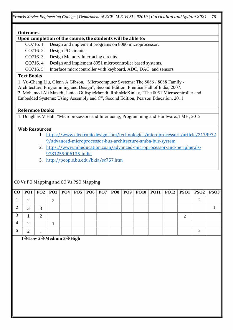
Francis Xavier Engineering College | Department of ECE |M.E-VLSI | R2019 | Curriculum and Syllabi 2021 78
Outcomes Upon completion of the course, the students will be able to:
CO716. 1 Design and implement programs on 8086 microprocessor.
CO716. 2 Design I/O circuits.
CO716. 3 Design Memory Interfacing circuits.
CO716. 4 Design and implement 8051 microcontroller based systems.
CO716. 5 Interface microcontroller with keyboard, ADC, DAC and sensors
Text Books
1. Yu-Cheng Liu, Glenn A.Gibson, “Microcomputer Systems: The 8086 / 8088 Family -
Architecture, Programming and Design”, Second Edition, Prentice Hall of India, 2007.
2. Mohamed Ali Mazidi, Janice GillispieMazidi, RolinMcKinlay, “The 8051 Microcontroller and
Embedded Systems: Using Assembly and C”, Second Edition, Pearson Education, 2011
Reference Books
1. Doughlas V.Hall, “Microprocessors and Interfacing, Programming and Hardware:,TMH, 2012
Web Resources 1. https://www.electronicdesign.com/technologies/microprocessors/article/2179972
9/advanced-microprocessor-bus-architecture-amba-bus-system
2. https://www.mheducation.co.in/advanced-microprocessor-and-peripherals-
9781259006135-india
3. http://people.bu.edu/bkia/sc757.htm
CO Vs PO Mapping and CO Vs PSO Mapping
1Low 2Medium 3High
CO PO1 PO2 PO3 PO4 PO5 PO6 PO7 PO8 PO9 PO10 PO11 PO12 PSO1 PSO2 PSO3
1 2 2 2
2 3 3 1
3 1 2 2
4 2 1
5 2 1 3
Related Documents