ME 141B: The MEMS Class Introduction to MEMS and MEMS Design Sumita Pennathur UCSB

Welcome message from author
This document is posted to help you gain knowledge. Please leave a comment to let me know what you think about it! Share it to your friends and learn new things together.
Transcript
ME 141B: The MEMS Class Introduction to MEMS and MEMS
Design
Sumita Pennathur UCSB

Outline today • Introduction to thin films • Oxidation
Deal-grove model
• CVD • Epitaxy • Electrodeposition
10/6/10 2/45

Creating thin (and thick) films
• Many techniques to choose from • Differences:
Front or back end processes Quality of resulting films (electrical properties, etch selectivity,
defects, residual stress) Conformality Deposition rate, cost
• Physical techniques Material is removed from a source, carried to the substrate, and
dropped there
• Chemical Techniques Reactants are transported to the substrate, a chemical reaction
occurs, and the product deposit on the substrate to form the desired film
10/6/10 3/45

Taxonomy of deposition techniques
• Chemical Thermal Oxidation Chemical Vapor Deposition (CVD)
• Low Pressure (LPCVD), Atomspheric pressure (APCVD), Plasma Enhanced (PECVD), Ultra High Vaccum CVD (UHCVD)
Epitaxy Electrodeposition (Electroplating)
• Physical Physical Vapor Deposition (PVD)
• Evaporation • Sputtering
Spin-casting
10/6/10 4/45

Thermal Oxidation • Most basic deposition technologies • Oxidation of a substrate surface in an O2 rich
atmosphere • Temperature is raised (800-1100C) to speed up process • Only deposition technology which CONSUMES substrate • Parabolic relationship between film thickness and
oxidation time for films thicker than ~100 nm
10/6/10 5/45

why is oxidation so important?
• Oxides are vital in device structures: gate oxide in MOS transistors field oxide for device isolation
• SiO2/Si has excellent electrical characteristics • Other desirable characteristics: excellent adhesion, non-
conductive, planar processing
*the ability to easily and reproducibly grow high-quality oxides on silicon is one of the principal
reasons for the importance of silicon to semiconductor devices!

When to use TO • Whenever you can! • Best, highest quality oxide • Unfortunately, high temperature makes it limited use • Typically used to form films that are used for electrical
insulation • Also used as etch masks or etch stops for future
processing steps
10/6/10 7/45

Oxidation I • Silicon forms a high quality, stable oxide
How it works: • Oxygen diffuses through oxide to SI/oxide interface • SI + O2 + high temperature (~1100) furnace SiO2 • Some Si is consumed
Rate determined by diffusion of oxygen through oxide Diffusion limits practical oxide thickness to < 2 um A key front end process
10/6/10 8/45

Oxidation II • Dry Oxidation (O2)
High quality, slow oxidation rate, smaller maximum thickness (i.e. gate oxide)
• Wet Oxidation (steam) H2 to speed the diffusion Lower quality, faster oxidation rate
• The Deal-Grove model describe the kinetics of oxidation quite well for oxides greater in thickness that about 30nm
10/6/10 9/45
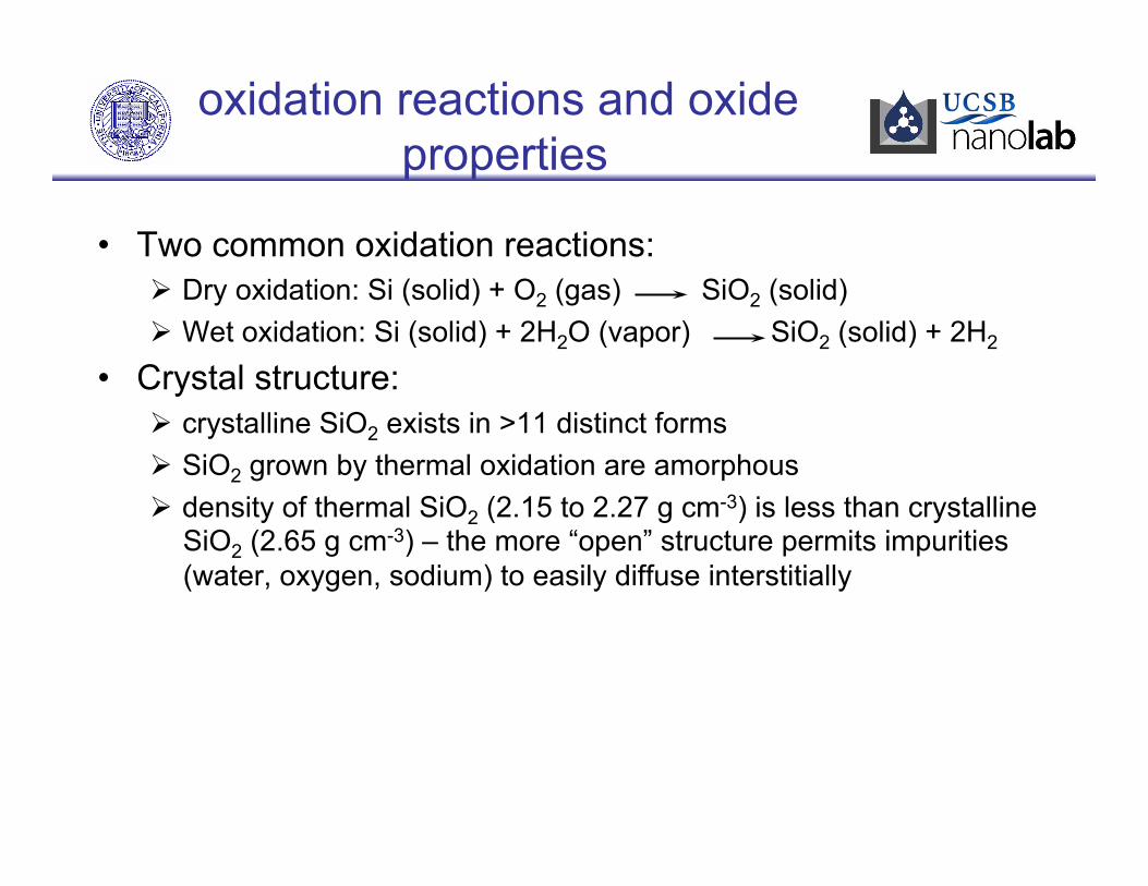
oxidation reactions and oxide properties
• Two common oxidation reactions: Dry oxidation: Si (solid) + O2 (gas) SiO2 (solid) Wet oxidation: Si (solid) + 2H2O (vapor) SiO2 (solid) + 2H2
• Crystal structure: crystalline SiO2 exists in >11 distinct forms SiO2 grown by thermal oxidation are amorphous density of thermal SiO2 (2.15 to 2.27 g cm-3) is less than crystalline
SiO2 (2.65 g cm-3) – the more “open” structure permits impurities (water, oxygen, sodium) to easily diffuse interstitially

oxide growth mechanism
• A film of growing SiO2 of thickness tox will consume a layer of crystalline Si of about 0.46 tox
• The oxide-Si interface is displaced from the original Si surface and is located deeper into the Si wafer
• With both O2 and H2O the oxidizing species moves through the oxide layer to react
• The displaced and deeper interface + inward migration of oxidizing species provides a clean, contaminant-free oxide-Si interface
0.46 tox tox

The Deal-Grove Model • Mathematically describes the growth of an oxide layer on
the surface of a material • Used to analyze thermal oxidation of silicon • Physical assumptions
Oxygen diffuses from the bulk to the ambient gas to the surface It diffuses through the existing oxide layer to the oxide-substrate
interface It then reacts with the substrate
• Model: Henry’s law Fick’s law of diffusion First-order reaction
• Also assume steady state conditions 10/6/10 12/45

The Deal-Grove Model
10/6/10 13/45

Deal Grove constants
Determine how long it takes to grow 1um of oxide on a bare silicon wafer at 1000C under both wet and dry conditions
t = xf2/BDG
47 minutes under wet conditions and 14.1 hours under dry conditions
10/6/10 14/45
Temperature ADG BDG 920 0.05 0.203 1000 0.226 0.287 1100 0.11 0.510

The Deal-Grove model
gas oxide silicon
Cg Cs Co Ci
F1 F2 F3
assumption: oxide growth occurs by diffusion of oxygen to the silicon interface, where the reaction Si + O2 → SiO2 occurs
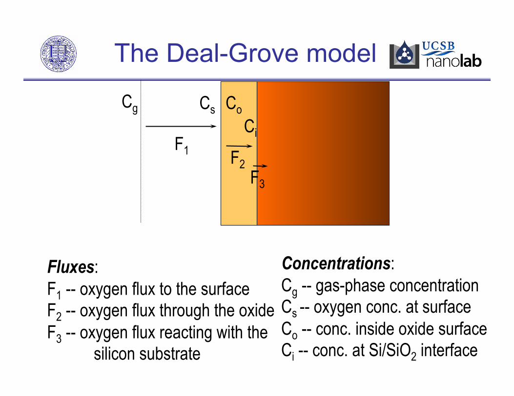
The Deal-Grove model
Cg Cs Co Ci
F1 F2 F3
Fluxes: F1 -- oxygen flux to the surface F2 -- oxygen flux through the oxide F3 -- oxygen flux reacting with the
silicon substrate
Concentrations: Cg -- gas-phase concentration Cs -- oxygen conc. at surface Co -- conc. inside oxide surface Ci -- conc. at Si/SiO2 interface

F1 -- Gas-phase diffusion flux
• Oxygen must diffuse across a stagnant boundary layer to the surface:
Cg Cs F1
where hg is the mass transport coefficient

F2 -- Oxide diffusion flux
• Oxygen must diffuse through the oxide to the silicon interface:
(note: the diffusivity is for oxygen in the oxide)
Co Ci
F2

F3 -- Oxide reaction flux
• The oxygen at the Si/SiO2 interface reacts to form the oxide:
Ci F3
where ks is the chemical rate constant for the oxidation reaction

Solution to the Deal-Grove model (1)
• at steady state (not equilibrium!) the fluxes will be equal:
F1 = F2 = F3 ≡ F • note that the oxygen concentration at the oxide
surface (Co) is proportional to the gas pressure (Henry’s Law)
Co= HPG =HkT CG since CG = n/V = PG /kT (ideal gas law)
• “After some algebra…” one obtains:
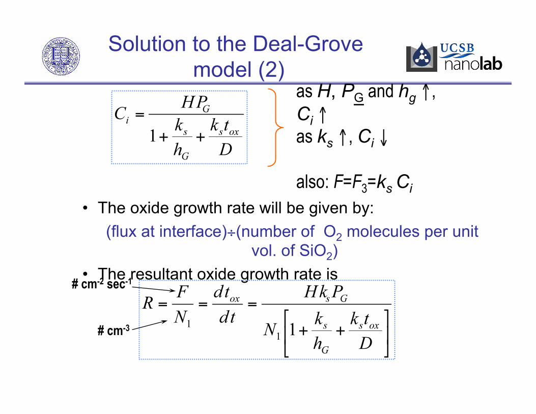
Solution to the Deal-Grove model (2)
• The oxide growth rate will be given by: (flux at interface)÷(number of O2 molecules per unit
vol. of SiO2) • The resultant oxide growth rate is
as H, PG and hg ↑, Ci ↑ as ks ↑, Ci ↓
also: F=F3=ks Ci
# cm-2 sec-1
# cm-3

Solution to the Deal-Grove model (3)
The solution to this differential equation is:
where

Evaluation of the Deal-Grove model
1. In most cases, oxidation is performed at atmospheric pressure where hG 〉〉 ks and A ≈2D/ks (units: cm)
2. Co = HPG so B = 2DCo/N1 (units: cm2 sec-1)
3. to is the oxide thickness at t = 0
where 1
2
3

Short times and thin oxides
• Early in the oxidation process the oxide thickness is linearly proportional to the oxidation time
• The ratio B/A is often called the “linear rate constant”
• B/A is equal to Coks/N1 and has units of cm sec-1 → independent of D
• τ arises from the boundary condition at t = 0 -- either the oxide thickness at t = 0 is to, or the thickness is zero at time –τ
t ≈ 0 and
or:

Long times and thick oxides
• B depends on the product of D and Co → a function of reactant concentration within the oxide and its ability to diffuse through the oxide
• B is often called the “parabolic rate constant” since a plot of the square of the thickness versus time would look like a parabola
• Systems that exhibit parabolic growth kinetics typically are diffusion controlled
and t >> τ
or:

The two limiting regimes
• Linear regime the growth rate is constant in time and is independent of the amount of gas and substrate that are consumed
• Parabolic regime a thermally-activated diffusion process is controlling the growth rate
• In general, the Deal-Grove model does an excellent job of describing the oxidation process under a wide variety of conditions

Observations on the linear regime
• Since the linear rate depends on the surface reaction rate, it can be sensitive to the properties of the substrate the linear rate constant for growth on the (111) Si surface is 1.7×
greater than for growth on the (100) surface (reason: larger number of available bonds on the (111) surface)
heavy doping of the silicon substrate can increase the linear rate constant by a factor of 10 -- doping enhanced oxidation, or DEO (reason: doping alters the interstitial and vacancy concentrations)
note: no effect on the parabolic rate constant (more to come on doping effects in oxidation…)
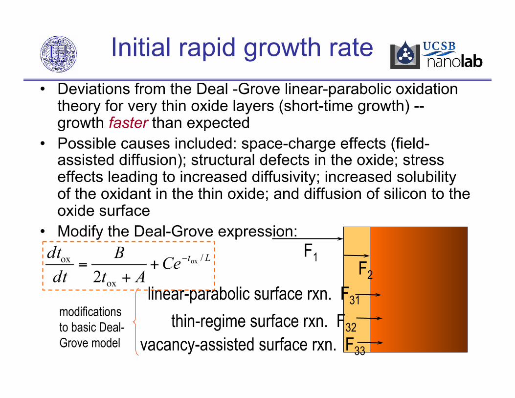
Initial rapid growth rate • Deviations from the Deal -Grove linear-parabolic oxidation
theory for very thin oxide layers (short-time growth) -- growth faster than expected
• Possible causes included: space-charge effects (field-assisted diffusion); structural defects in the oxide; stress effects leading to increased diffusivity; increased solubility of the oxidant in the thin oxide; and diffusion of silicon to the oxide surface
• Modify the Deal-Grove expression: F1
F2 linear-parabolic surface rxn. F31
thin-regime surface rxn. F32 vacancy-assisted surface rxn. F33
modifications to basic Deal- Grove model

Observations on the parabolic regime
• The parabolic rate constant is sensitive to factors that alter the ability of the oxidizing species to diffuse through the oxide H2O is a smaller molecule than O2 and thus will have a
larger diffusion coefficient The oxide formed by wet oxidation is more porous and
less dense than that formed without water (dry oxidation) and permits higher diffusivities at lower temperatures
• Increasing the oxygen pressure will also increase B and decrease the time needed to grow a thick oxide

A sample calculation A silicon wafer is initially covered by an SiO2 film 0.3 µm thick. What is the time required to increase the thickness to 0.5 µm?
(ignore τ for thick oxide) For a wet oxidation at 1200oC, A = 0.05 µm and B = 0.720 µm2/hr, so: (0.2)2 + (0.05)(.2) = (0.720)t or t = 0.069 hours or ~ 4.2 minutes If a dry oxidation at is performed at 1200oC, A = 0.04 µm and B = 0.045 µm2/hr, so: (0.2)2 + (0.04)(.2) = (0.045)t or t = 1.067 hours or ~ 64 minutes

Interference measurement of oxide thickness
By measuring the intensity of reflected light as a function of wavelength, the oxide thickness can be determined from:
Io
tox nox
φ
strictly true only at normal incidence

• Interference effects can give a thin transparent layer a characteristic color
• Color depends on: film thickness index of refraction spectral distribution of the viewing light
• Experienced viewers can estimate the thickness of a film to about 100Å

Physical characterization of oxides -- ellipsometry
• As light is reflected from a surface, it is normally reduced in amplitude and shifted in phase
• If there are multiple reflecting layers, the various beams will interact further with each other
unpolarized plane polarized into components p and s
p s
φ φ plane
polarized elliptically polarized components differ in phase & amplitude
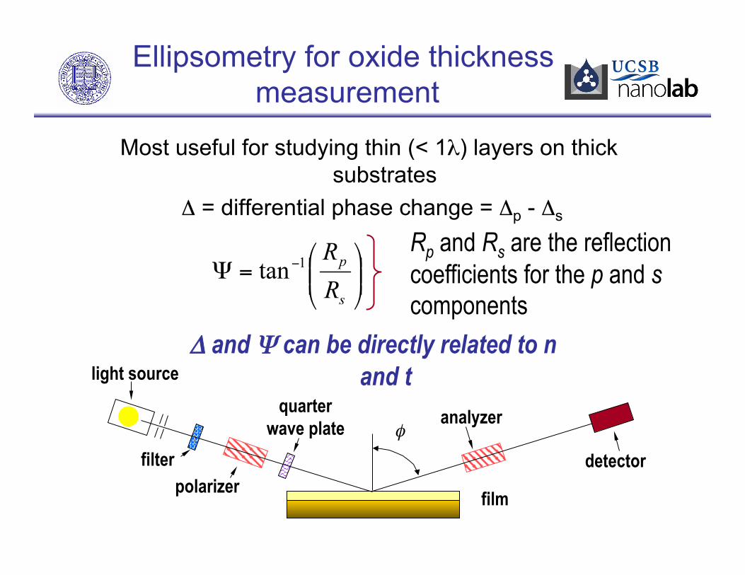
Ellipsometry for oxide thickness measurement
Most useful for studying thin (< 1λ) layers on thick substrates
Δ = differential phase change = Δp - Δs Rp and Rs are the reflection coefficients for the p and s components
φ quarter
wave plate
light source
filter polarizer film
analyzer
detector
Δ and Ψ can be directly related to n and t

Validity of Model • Works well for single=crystal silicon • Thin oxides grow more quickly in O2 • Fails for polycrystalline silicon
Random orientation of the crystal grains makes it difficult to choose value for linear rate constant
Oxidant molecules diffuse rapidly along grain boundaries – oxidizes more rapidly
• Dopants strain silicon lattice – making it easier for oxygen to enter – oxidizes faster
10/6/10 35/45
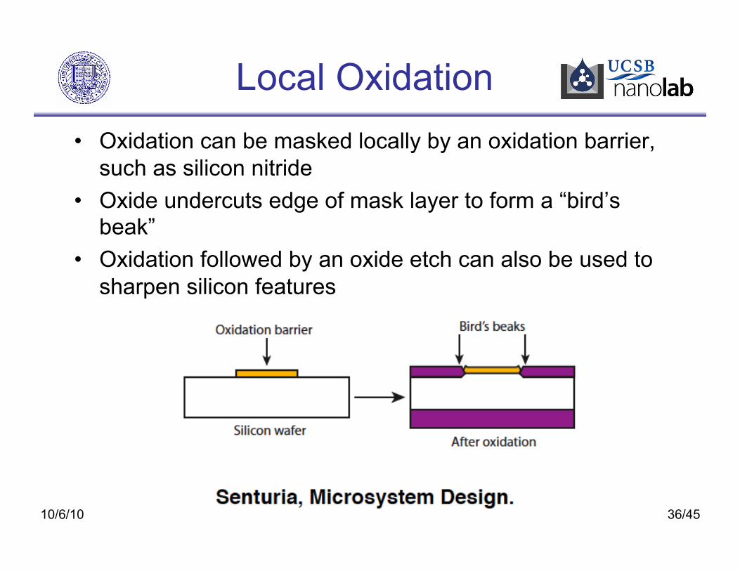
Local Oxidation • Oxidation can be masked locally by an oxidation barrier,
such as silicon nitride • Oxide undercuts edge of mask layer to form a “bird’s
beak” • Oxidation followed by an oxide etch can also be used to
sharpen silicon features
10/6/10 36/45
CVD • CVD is a chemical process used to produce high-purity,
high-performance solid materials • Typical CVD process
Wafer exposed to one or more volatile precursers These react and/or decompose on surface This produces desired deposit
• Can deposit in various forms Monocrystaline Polycrystalline Amorphous Epitaxial
• Materials include silicon, carbon fiber, carbon nanofibers, filaments, carbon nanotubes, SiO2, silicon-germanium, tungsten, silicon carbide, silicon nitride, etc… 10/6/10 37/45
Chemical Vapor Deposition (CVD)
• How CVD works: Gaseous reactants, often at low pressure Long mean free path; reactants reach substrate Reactants react and deposit products on the substrate Unlike Oxidation, does not consume substrate material
• Energy sources facilitate CVD reactions: High temperature, plasma, laser
• Processing temperatures vary widely • Commonly deposited films: Oxide, silicon nitride,
polysilicon • CVD results depend on pressures, gas flows,
temperature Film composition, uniformity, deposition rate, and electrical and
mechanical characteristics can vary 10/6/10 38/45

Types of CVD • Atmospheric pressure CVD (SPCVD) – CVD processes
at atmospheric pressure • Low Pressure CVD (LPCVD)- CVD processes at
subatmospheric pressures. Reduced pressures tend to reduce unwanted gas-phase reaction
and improve uniformity across the wafer Most modern CVD processes are LPCVD or UHCVD
• Ultrahigh vacuum CVD (UHCVD) – CVD process at a very low pressure, ~10-8 torr
• Plasma-enhanced CVD (PECVD) – CVD process that utilize a plasma to enhance chemical reaction rates of the precursors Allows low temperatures
• Other types, MPCVD, ALCVD, MOCVD 10/6/10 39/45

Some reasons to use CVD • Oxide formation:
To get a thicker layer than thermal oxidation can provide To create oxide on a wafer that can’t withstand high
temperatures (for example because of metal features) To create oxide on top of a material that is not silicon
• For film formation in general To tailor the film properties (like form stress) by adjusting
pressures, flow rates, external energy supply, ratios of different precursor gases (to adjust proportions of different materials in the final product)
Conformailty : (more of less) even coating on all surfaces • Drawbacks:
Films deposited at low temperature are often lower quality than high temp versions, and have less predictable properties
Flammable, toxic or corrosive source gases 10/6/10 40/45
Thick Film Formation • CVD is a common MEMS tool for creating thick films on
the wafer surface In practice, film stress limits thickness (film delamination or
cracking, or curvature of underlying structures) Can deposit thick oxides; nitrides are still typically submicron Must anneal deposited oxides for some applications – lose low
stress property on anneal
10/6/10 41/45

Commonly Deposited Substances
• Polysilicon Deposited from silane (SH4) (SiH4 Si + 2H2) Usually preformed in LPCVD systems Growth rate 10-20 nm per minute
• Silicon dioxide Source gases include silane and oxygen, dichlorosilane, nitrous
oxide, or TEOS (tetraethlyorthosilicate) Choice of source depends on thermal stability of substrates
• ie. aluminum is sensitive to high temperature TEOS is the best, but needs 650-700C, silane is lower quality.
Thermal oxidation is best Ozone may deposit TEOS at lower temperatures – being
explored
10/6/10 42/45

Commonly Deposited Substrates
• Silicon Nitride LPCVD generally used here
• Metals Molybdenum, tatalum, titatnium, nickel and tungsten Deposited by LPCVD
10/6/10 43/45

CVD enables conformal coating
10/6/10 44/45

LPCVD Polysilicon • Amorphous at lower deposition temperatures and high
deposition rates Typical temperature: ~590 C
• Polycrystalline at higher deposition temperatures and lower deposition rates Typical temperature: ~625 C
• Grain size and structure depend on detailed deposition conditions E.g. thicker films larger grains
• Structure, electrical properties, and mechanical properties also vary with post-deposition thermal processing Grain growth Dpoant activation or diffusion 10/6/10 45/45

CVD Machine
10/6/10 46/45

Epitaxy • CVD deposition process in which atoms move to lattice
sites, continuing the substrate’s crystal structure Homoepitaxy: same material, i.e. Si on Si Heteroepitaxy: different materials, i.e. AlGaAs, on GaAs
• How it happens Slow deposition rate (enough time to find a lattice site) High Temperature (enough energy to move a lattice site)
• Selective epitaxy is possible through masking • Can grow a doped Si layer of known thickness
10/6/10 47/45
Electroplating: basics • Pass a current through an aqueous metal solution
Anode is made of the meta that you want to deposit Cathode is the conductive seed material on your wafer Positive metal ions travel to the negatively charged cathode on
your wafer and deposit there
• Preparing your wafer If you want to plate metal in some places and not in others, you
will need a patterned metal seed layer (and typically a “sticky” metal adhesion layer under that)
For very short features, just plate onto the seed layer For taller features, need to plate into a mold Molds can be photoresist, silicon, SU-8, et.. Depending on the
needs of your device
10/6/10 48/45
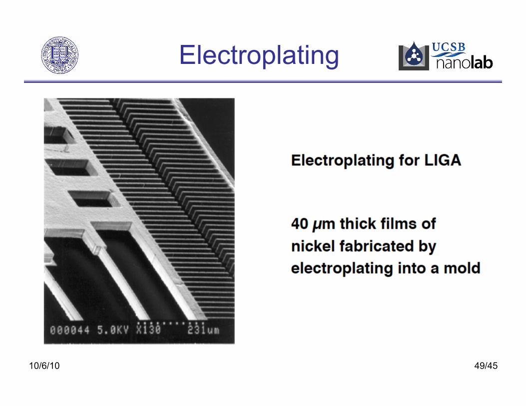
Electroplating
10/6/10 49/45

Electroplating realities
10/6/10 50/45
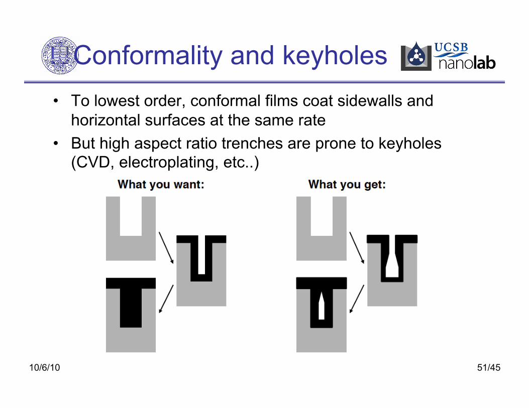
Conformality and keyholes • To lowest order, conformal films coat sidewalls and
horizontal surfaces at the same rate • But high aspect ratio trenches are prone to keyholes
(CVD, electroplating, etc..)
10/6/10 51/45
Related Documents