© 2007 Microchip Technology Inc. DS21801E-page 1 MCP2515 Features • Implements CAN V2.0B at 1 Mb/s: - 0 – 8 byte length in the data field - Standard and extended data and remote frames • Receive buffers, masks and filters: - Two receive buffers with prioritized message storage - Six 29-bit filters - Two 29-bit masks • Data byte filtering on the first two data bytes (applies to standard data frames) • Three transmit buffers with prioritizaton and abort features • High-speed SPI Interface (10 MHz): - SPI modes 0,0 and 1,1 • One-shot mode ensures message transmission is attempted only one time • Clock out pin with programmable prescaler: - Can be used as a clock source for other device(s) • Start-of-Frame (SOF) signal is available for monitoring the SOF signal: - Can be used for time-slot-based protocols and/or bus diagnostics to detect early bus degredation • Interrupt output pin with selectable enables • Buffer Full output pins configurable as: - Interrupt output for each receive buffer - General purpose output • Request-to-Send (RTS) input pins individually configurable as: - Control pins to request transmission for each transmit buffer - General purpose inputs • Low-power CMOS technology: - Operates from 2.7V – 5.5V - 5 mA active current (typical) - 1 μA standby current (typical) (Sleep mode) • Temperature ranges supported: - Industrial (I): -40°C to +85°C - Extended (E): -40°C to +125°C Description Microchip Technology’s MCP2515 is a stand-alone Controller Area Network (CAN) controller that imple- ments the CAN specification, version 2.0B. It is capable of transmitting and receiving both standard and extended data and remote frames. The MCP2515 has two acceptance masks and six acceptance filters that are used to filter out unwanted messages, thereby reducing the host MCUs overhead. The MCP2515 interfaces with microcontrollers (MCUs) via an industry standard Serial Peripheral Interface (SPI). Package Types TXCAN RXCAN VDD RESET CS SO MCP2515 1 2 3 4 18 17 16 15 SI SCK INT RX0BF 14 13 12 11 RX1BF 10 OSC2 OSC1 CLKOUT/SOF TX2RTS 5 6 7 8 Vss 9 TX0RTS TX1RTS MCP2515 TXCAN RXCAN TX0RTS OSC1 CLKOUT/SOF OSC2 CS VDD RESET SO SCK INT SI RX0BF RX1BF VSS TX1RTS TX2RTS NC NC 13 12 1 2 3 4 5 6 7 8 9 20 19 18 17 16 15 14 11 10 18-Lead PDIP/SOIC 20-LEAD TSSOP Stand-Alone CAN Controller With SPI Interface

Welcome message from author
This document is posted to help you gain knowledge. Please leave a comment to let me know what you think about it! Share it to your friends and learn new things together.
Transcript

MCP2515Stand-Alone CAN Controller With SPI Interface
Features• Implements CAN V2.0B at 1 Mb/s:
- 0 – 8 byte length in the data field- Standard and extended data and remote
frames • Receive buffers, masks and filters:
- Two receive buffers with prioritized message storage
- Six 29-bit filters- Two 29-bit masks
• Data byte filtering on the first two data bytes (applies to standard data frames)
• Three transmit buffers with prioritizaton and abort features
• High-speed SPI Interface (10 MHz):- SPI modes 0,0 and 1,1
• One-shot mode ensures message transmission is attempted only one time
• Clock out pin with programmable prescaler:- Can be used as a clock source for other
device(s)• Start-of-Frame (SOF) signal is available for
monitoring the SOF signal:- Can be used for time-slot-based protocols
and/or bus diagnostics to detect early bus degredation
• Interrupt output pin with selectable enables• Buffer Full output pins configurable as:
- Interrupt output for each receive buffer- General purpose output
• Request-to-Send (RTS) input pins individually configurable as:- Control pins to request transmission for each
transmit buffer- General purpose inputs
• Low-power CMOS technology:- Operates from 2.7V – 5.5V- 5 mA active current (typical)- 1 µA standby current (typical) (Sleep mode)
• Temperature ranges supported:- Industrial (I): -40°C to +85°C- Extended (E): -40°C to +125°C
DescriptionMicrochip Technology’s MCP2515 is a stand-aloneController Area Network (CAN) controller that imple-ments the CAN specification, version 2.0B. It is capableof transmitting and receiving both standard andextended data and remote frames. The MCP2515 hastwo acceptance masks and six acceptance filters thatare used to filter out unwanted messages, therebyreducing the host MCUs overhead. The MCP2515interfaces with microcontrollers (MCUs) via an industrystandard Serial Peripheral Interface (SPI).
Package Types
TXCAN
RXCAN
VDD
RESET
CS
SO
MC
P251
5
1
2
3
4
18
17
16
15
SI
SCK
INT
RX0BF
14
13
12
11
RX1BF10
OSC2
OSC1
CLKOUT/SOF
TX2RTS
5
6
7
8Vss 9
TX0RTS
TX1RTS
MC
P251
5
TXCANRXCAN
TX0RTS
OSC1
CLKOUT/SOF
OSC2
CS
VDD
RESET
SO
SCKINT
SI
RX0BFRX1BFVSS
TX1RTS
TX2RTSNC NC
1312
123456789
20191817161514
1110
18-Lead PDIP/SOIC
20-LEAD TSSOP
© 2007 Microchip Technology Inc. DS21801E-page 1

MCP2515
NOTES:DS21801E-page 2 © 2007 Microchip Technology Inc.

MCP2515
1.0 DEVICE OVERVIEWThe MCP2515 is a stand-alone CAN controllerdeveloped to simplify applications that requireinterfacing with a CAN bus. A simple block diagram ofthe MCP2515 is shown in Figure 1-1. The deviceconsists of three main blocks:
1. The CAN module, which includes the CANprotocol engine, masks, filters, transmit andreceive buffers.
2. The control logic and registers that are used toconfigure the device and its operation.
3. The SPI protocol block.
An example system implementation using the device isshown in Figure 1-2.
1.1 CAN ModuleThe CAN module handles all functions for receivingand transmitting messages on the CAN bus. Messagesare transmitted by first loading the appropriatemessage buffer and control registers. Transmission isinitiated by using control register bits via the SPIinterface or by using the transmit enable pins. Statusand errors can be checked by reading the appropriateregisters. Any message detected on the CAN bus ischecked for errors and then matched against the user-defined filters to see if it should be moved into one ofthe two receive buffers.
1.2 Control LogicThe control logic block controls the setup and operationof the MCP2515 by interfacing to the other blocks inorder to pass information and control.
Interrupt pins are provided to allow greater systemflexibility. There is one multi-purpose interrupt pin (aswell as specific interrupt pins) for each of the receiveregisters that can be used to indicate a valid messagehas been received and loaded into one of the receivebuffers. Use of the specific interrupt pins is optional.The general purpose interrupt pin, as well as statusregisters (accessed via the SPI interface), can also beused to determine when a valid message has beenreceived.
Additionally, there are three pins available to initiateimmediate transmission of a message that has beenloaded into one of the three transmit registers. Use ofthese pins is optional, as initiating messagetransmissions can also be accomplished by utilizingcontrol registers, accessed via the SPI interface.
1.3 SPI Protocol BlockThe MCU interfaces to the device via the SPI interface.Writing to, and reading from, all registers isaccomplished using standard SPI read and writecommands, in addition to specialized SPI commands.
FIGURE 1-1: BLOCK DIAGRAM
SPIInterface
LogicSPIBus
INT
CSSCKSISO
CANProtocolEngine
RXCAN
TXCAN
Control Logic
RX0BFRX1BFTX0RTSTX1RTSTX2RTS
TX and RX Buffers
Masks and Filters
CAN Module
RESET
TimingGeneration
OSC1OSC2
CLKOUT
Controland
InterruptRegisters
© 2007 Microchip Technology Inc. DS21801E-page 3

MCP2515
FIGURE 1-2: EXAMPLE SYSTEM IMPLEMENTATIONTABLE 1-1: PINOUT DESCRIPTION
Name PDIP/SOICPin #
TSSOP Pin #
I/O/P Type Description Alternate Pin Function
TXCAN 1 1 O Transmit output pin to CAN bus —
RXCAN 2 2 I Receive input pin from CAN bus —
CLKOUT 3 3 O Clock output pin with programmable prescaler
Start-of-Frame signal
TX0RTS 4 4 I Transmit buffer TXB0 request-to-send. 100 kΩ internal pull-up to VDD
General purpose digital input.100 kΩ internal pull-up to VDD
TX1RTS 5 5 I Transmit buffer TXB1 request-to-send. 100 kΩ internal pull-up to VDD
General purpose digital input.100 kΩ internal pull-up to VDD
TX2RTS 6 7 I Transmit buffer TXB2 request-to-send. 100 kΩ internal pull-up to VDD
General purpose digital input.100 kΩ internal pull-up to VDD
OSC2 7 8 O Oscillator output —
OSC1 8 9 I Oscillator input External clock input
VSS 9 10 P Ground reference for logic and I/O pins —
RX1BF 10 11 O Receive buffer RXB1 interrupt pin or general purpose digital output
General purpose digital output
RX0BF 11 12 O Receive buffer RXB0 interrupt pin or general purpose digital output
General purpose digital output
INT 12 13 O Interrupt output pin —
SCK 13 14 I Clock input pin for SPI interface —
SI 14 16 I Data input pin for SPI interface —
SO 15 17 O Data output pin for SPI interface —
CS 16 18 I Chip select input pin for SPI interface —
RESET 17 19 I Active low device reset input —
VDD 18 20 P Positive supply for logic and I/O pins —
NC — 6,15 — No internal connection
Note: Type Identification: I = Input; O = Output; P = Power
NodeController
MCP2515
XCVR
SPI
TX RX
CANHCANL
NodeController
MCP2515
XCVR
SPI
TX RX
NodeController
MCP2515
XCVR
SPI
TX RX
DS21801E-page 4 © 2007 Microchip Technology Inc.

MCP2515
1.4 Transmit/Receive Buffers/Masks/FiltersThe MCP2515 has three transmit and two receivebuffers, two acceptance masks (one for each receivebuffer) and a total of six acceptance filters. Figure 1-3shows a block diagram of these buffers and theirconnection to the protocol engine.
FIGURE 1-3: CAN BUFFERS AND PROTOCOL ENGINE BLOCK DIAGRAM
Acceptance FilterRXF2
RXB1
Identifier
Data Field Data Field
Identifier
Acceptance MaskRXM1
Acceptance FilterRXF3
Acceptance FilterRXF4
Acceptance FilterRXF5
MAB
Acceptance FilterRXF0
Acceptance FilterRXF1
RXB0
TXR
EQ
TXB2A
BTF
MLO
ATX
ER
R
ME
SS
AG
E
MessageQueueControl Transmit Byte Sequencer
TXR
EQ
TXB0
AB
TFM
LOA
TXE
RR
ME
SS
AG
E
CRC<14:0>
Comparator
Receive<7:0>Transmit<7:0>
ReceiveError
TransmitError
Protocol
REC
TEC
ErrPasBusOff
FiniteState
Machine
Counter
Counter
Shift<14:0>{Transmit<5:0>, Receive<8:0>}
TransmitLogic
BitTimingLogic
TX RXConfiguration
Registers
ClockGenerator
PROTOCOLENGINE
BUFFERS
TXR
EQ
TXB1
AB
TFM
LOA
TXE
RR
ME
SS
AG
E
Acceptance MaskRXM0
Accept
Accept
SOF
© 2007 Microchip Technology Inc. DS21801E-page 5

MCP2515
1.5 CAN Protocol EngineThe CAN protocol engine combines several functionalblocks, shown in Figure 1-4 and described below.1.5.1 PROTOCOL FINITE STATE MACHINE
The heart of the engine is the Finite State Machine(FSM). The FSM is a sequencer that controls thesequential data stream between the TX/RX shiftregister, the CRC register and the bus line. The FSMalso controls the Error Management Logic (EML) andthe parallel data stream between the TX/RX shiftregisters and the buffers. The FSM ensures that theprocesses of reception, arbitration, transmission anderror-signaling are performed according to the CANprotocol. The automatic retransmission of messageson the bus line is also handled by the FSM.
1.5.2 CYCLIC REDUNDANCY CHECK
The Cyclic Redundancy Check register generates theCyclic Redundancy Check (CRC) code, which istransmitted after either the Control Field (for messageswith 0 data bytes) or the Data Field and is used tocheck the CRC field of incoming messages.
1.5.3 ERROR MANAGEMENT LOGIC
The Error Management Logic (EML) is responsible forthe fault confinement of the CAN device. Its twocounters, the Receive Error Counter (REC) and theTransmit Error Counter (TEC), are incremented anddecremented by commands from the bit streamprocessor. Based on the values of the error counters,the CAN controller is set into the states error-active,error-passive or bus-off.
1.5.4 BIT TIMING LOGIC
The Bit Timing Logic (BTL) monitors the bus line inputand handles the bus-related bit timing according to theCAN protocol. The BTL synchronizes on a recessive-to-dominant bus transition at Start-of-Frame (hard syn-chronization) and on any further recessive-to-dominantbus line transition if the CAN controller itself does nottransmit a dominant bit (resynchronization). The BTLalso provides programmable time segments tocompensate for the propagation delay time, phaseshifts and to define the position of the sample pointwithin the bit time. The programming of the BTLdepends on the baud rate and external physical delaytimes.
FIGURE 1-4: CAN PROTOCOL ENGINE BLOCK DIAGRAM
Bit Timing Logic
CRC<14:0>
Comparator
Receive<7:0> Transmit<7:0>
Sample<2:0>
MajorityDecision
StuffReg<5:0>
Comparator
Transmit Logic
ReceiveError Counter
TransmitError Counter
ProtocolFSM
RX
SAM
BusMon
Rec/Trm Addr.
RecData<7:0> TrmData<7:0>
Shift<14:0>(Transmit<5:0>, Receive<7:0>)
TX
REC
TEC
ErrPasBusOff
Interface to Standard Buffer
SOF
DS21801E-page 6 © 2007 Microchip Technology Inc.

MCP2515
2.0 CAN MESSAGE FRAMESThe MCP2515 supports standard data frames,extended data frames and remote frames (standardand extended), as defined in the CAN 2.0Bspecification.
2.1 Standard Data FrameThe CAN standard data frame is shown in Figure 2-1.As with all other frames, the frame begins with a Start-Of-Frame (SOF) bit, which is of the dominant state andallows hard synchronization of all nodes.
The SOF is followed by the arbitration field, consistingof 12 bits: the 11-bit identifier and the RemoteTransmission Request (RTR) bit. The RTR bit is usedto distinguish a data frame (RTR bit dominant) from aremote frame (RTR bit recessive).
Following the arbitration field is the control field,consisting of six bits. The first bit of this field is theIdentifier Extension (IDE) bit, which must be dominantto specify a standard frame. The following bit, ReservedBit Zero (RB0), is reserved and is defined as a dominantbit by the CAN protocol. The remaining four bits of thecontrol field are the Data Length Code (DLC), whichspecifies the number of bytes of data (0 – 8 bytes)contained in the message.
After the control field is the data field, which containsany data bytes that are being sent, and is of the lengthdefined by the DLC (0 – 8 bytes).
The Cyclic Redundancy Check (CRC) field follows thedata field and is used to detect transmission errors. TheCRC field consists of a 15-bit CRC sequence, followedby the recessive CRC Delimiter bit.
The final field is the two-bit Acknowledge (ACK) field.During the ACK Slot bit, the transmitting node sendsout a recessive bit. Any node that has received anerror-free frame acknowledges the correct reception ofthe frame by sending back a dominant bit (regardlessof whether the node is configured to accept thatspecific message or not). The recessive acknowledgedelimiter completes the acknowledge field and may notbe overwritten by a dominant bit.
2.2 Extended Data FrameIn the extended CAN data frame, shown in Figure 2-2,the SOF bit is followed by the arbitration field, whichconsists of 32 bits. The first 11 bits are the MostSignificant bits (MSb) (Base-lD) of the 29-bit identifier.These 11 bits are followed by the Substitute RemoteRequest (SRR) bit, which is defined to be recessive.The SRR bit is followed by the lDE bit, which isrecessive to denote an extended CAN frame.
It should be noted that if arbitration remains unresolvedafter transmission of the first 11 bits of the identifier, andone of the nodes involved in the arbitration is sendinga standard CAN frame (11-bit identifier), the standard
CAN frame will win arbitration due to the assertion of adominant lDE bit. Also, the SRR bit in an extendedCAN frame must be recessive to allow the assertion ofa dominant RTR bit by a node that is sending astandard CAN remote frame.
The SRR and lDE bits are followed by the remaining18 bits of the identifier (Extended lD) and the remotetransmission request bit.
To enable standard and extended frames to be sentacross a shared network, the 29-bit extended messageidentifier is split into 11-bit (most significant) and 18-bit(least significant) sections. This split ensures that thelDE bit can remain at the same bit position in both thestandard and extended frames.
Following the arbitration field is the six-bit control field.The first two bits of this field are reserved and must bedominant. The remaining four bits of the control fieldare the DLC, which specifies the number of data bytescontained in the message.
The remaining portion of the frame (data field, CRCfield, acknowledge field, end-of-frame and intermis-sion) is constructed in the same way as a standard dataframe (see Section 2.1 “Standard Data Frame”).
2.3 Remote FrameNormally, data transmission is performed on anautonomous basis by the data source node (e.g., asensor sending out a data frame). It is possible,however, for a destination node to request data fromthe source. To accomplish this, the destination nodesends a remote frame with an identifier that matchesthe identifier of the required data frame. Theappropriate data source node will then send a dataframe in response to the remote frame request.
There are two differences between a remote frame(shown in Figure 2-3) and a data frame. First, the RTRbit is at the recessive state and, second, there is nodata field. In the event of a data frame and a remoteframe with the same identifier being transmitted at thesame time, the data frame wins arbitration due to thedominant RTR bit following the identifier. In this way,the node that transmitted the remote frame receivesthe desired data immediately.
2.4 Error FrameAn error frame is generated by any node that detects abus error. An error frame, shown in Figure 2-4, consistsof two fields: an error flag field followed by an errordelimiter field. There are two types of error flag fields.The type of error flag field sent depends upon the errorstatus of the node that detects and generates the errorflag field.
© 2007 Microchip Technology Inc. DS21801E-page 7

MCP2515
2.4.1 ACTIVE ERRORSIf an error-active node detects a bus error, the nodeinterrupts transmission of the current message bygenerating an active error flag. The active error flag iscomposed of six consecutive dominant bits. This bitsequence actively violates the bit-stuffing rule. All otherstations recognize the resulting bit-stuffing error and, inturn, generate error frames themselves, called errorecho flags.The error flag field, therefore, consists of between sixand twelve consecutive dominant bits (generated byone or more nodes). The error delimiter field (eightrecessive bits) completes the error frame. Uponcompletion of the error frame, bus activity returns tonormal and the interrupted node attempts to resend theaborted message.
2.4.2 PASSIVE ERRORSIf an error-passive node detects a bus error, the nodetransmits an error-passive flag followed by the errordelimiter field. The error-passive flag consists of sixconsecutive recessive bits. The error frame for an error-passive node consists of 14 recessive bits. From this itfollows that, unless the bus error is detected by an error-active node or the transmitting node, the message willcontinue transmission because the error-passive flagdoes not interfere with the bus.
If the transmitting node generates an error-passive flag,it will cause other nodes to generate error frames dueto the resulting bit-stuffing violation. After transmissionof an error frame, an error-passive node must wait forsix consecutive recessive bits on the bus beforeattempting to rejoin bus communications.
The error delimiter consists of eight recessive bits andallows the bus nodes to restart bus communicationscleanly after an error has occurred.
2.5 Overload FrameAn overload frame, shown in Figure 2-5, has the sameformat as an active error frame. An overload frame,however, can only be generated during an interframespace. In this way, an overload frame can be differenti-ated from an error frame (an error frame is sent duringthe transmission of a message). The overload frameconsists of two fields: an overload flag followed by anoverload delimiter. The overload flag consists of sixdominant bits followed by overload flags generated byother nodes (and, as for an active error flag, giving amaximum of twelve dominant bits). The overloaddelimiter consists of eight recessive bits. An overloadframe can be generated by a node as a result of twoconditions:
1. The node detects a dominant bit during theinterframe space, an illegal condition.Exception: The dominant bit is detected duringthe third bit of IFS. In this case, the receivers willinterpret this as a SOF.
2. Due to internal conditions, the node is not yetable to begin reception of the next message. Anode may generate a maximum of twosequential overload frames to delay the start ofthe next message.
2.6 Interframe SpaceThe interframe space separates a preceding frame (ofany type) from a subsequent data or remote frame.The interframe space is composed of at least threerecessive bits called the Intermission. This allowsnodes time for internal processing before the start ofthe next message frame. After the intermission, thebus line remains in the recessive state (bus idle) untilthe next transmission starts.
Note: Error echo flags typically occur when alocalized disturbance causes one or more(but not all) nodes to send an error flag.The remaining nodes generate error flagsin response (echo) to the original errorflag.
Note: Case 2 should never occur with theMCP2515 due to very short internaldelays.
DS21801E-page 8 © 2007 Microchip Technology Inc.

MCP2515
FIGURE 2-1: STANDARD DATA FRAME00
00
11
11
11
11
Start-of-Frame
Dat
a Fr
ame
(num
ber o
f bits
= 4
4 +
8N)
12A
rbitr
atio
n Fi
eld
ID 10
11
ID3
ID0
Iden
tifie
r
Mes
sage
Filte
ring
Stor
ed in
Buf
fers
RTRIDERB0DLC3
DLC06
4
Con
trol
Fiel
d Dat
aLe
ngth
Cod
e
Reserved Bit
8N (0
≤N≤8
)D
ata
Fiel
d
88
Stor
ed in
Tra
nsm
it/R
ecei
ve B
uffe
rs
Bit-
stuf
fing
16C
RC
Fie
ld
15 CR
C
7
End-
of-
Fram
e
CRC DelAck Slot BitACK Del
IFS
11
11
© 2007 Microchip Technology Inc. DS21801E-page 9

MCP2515
FIGURE 2-2: EXTENDED DATA FRAME01
10
00
1
Start-Of-Frame
Arb
itrat
ion
Fiel
d32
11
ID10
ID3
ID0
IDE
Iden
tifie
r
Mes
sage
Filte
ring
Stor
ed in
Buf
fers
SRR
EID17
EID0RTRRB1RB0DLC3
18
DLC0
6C
ontro
lFi
eld 4
Reserved bitsD
ata
Leng
thC
ode St
ored
in T
rans
mit/
Rec
eive
Buf
fers
88
Dat
a Fr
ame
(num
ber o
f bits
= 6
4 +
8N)
8N (0
≤ N
≤ 8
)D
ata
Fiel
d
11
11
11
11
16C
RC
Fie
ld
15 CR
C
CRC DelAck Slot BitACK Del
End-
of-
Fram
e
7
Bit-
stuf
fing
IFS
Ext
ende
d Id
entif
ier
11
1
DS21801E-page 10 © 2007 Microchip Technology Inc.

MCP2515
FIGURE 2-3: REMOTE FRAME01
11
00
Start-Of-Frame
Arb
itrat
ion
Fiel
d
32
11
ID10
ID3
ID0
IDE
Iden
tifie
r
Mes
sage
Filte
ring
SRR
EID17
EID0RTRRB1RB0DLC3
18
DLC0
6C
ontro
lFi
eld 4
Reserved bits
Dat
aLe
ngth
Cod
e
Ext
ende
d Id
entif
ier
11
11
11
11
1
16C
RC
Fie
ld
15 CR
C
CRC DelAck Slot BitACK Del
End
-of-
Fram
e
7
Rem
ote
Fram
e w
ith E
xten
ded
Iden
tifie
r
11
1
IFS
No
data
fiel
d
© 2007 Microchip Technology Inc. DS21801E-page 11

MCP2515
FIGURE 2-4: ACTIVE ERROR FRAME00
00
Start-Of-Frame
Inte
rrup
ted
Dat
a Fr
ame
12A
rbitr
atio
n Fi
eld
ID 10
11
ID3
ID0
Iden
tifie
r
Mes
sage
Filte
ring
RTRIDERB0DLC3
DLC0
6
4
Con
trol
Fiel
d Dat
aLe
ngth
Cod
e
Reserved Bit
8N (0
≤N≤8
)D
ata
Fiel
d
88
Bit-
stuf
fing
00
00
00
00
01
11
11
11
10
Dat
a Fr
ame
orR
emot
e Fr
ame
Err
or F
ram
e
6E
rror
Flag
£ 6
Ech
oE
rror
Flag
8
Erro
rD
elim
iter
Inte
r-Fr
ame
Spac
e or
Ove
rload
Fra
me
DS21801E-page 12 © 2007 Microchip Technology Inc.

MCP2515
FIGURE 2-5: OVERLOAD FRAME01
00
11
11
11
11
1
Start-Of-Frame
Rem
ote
Fram
e (n
umbe
r of b
its =
44)
12A
rbitr
atio
n Fi
eld
ID 10
11
ID0RTRIDERB0DLC3
DLC0
6
4
Con
trol
Fiel
d
16C
RC
Fie
ld
15 CR
C
7
End
-of-
Fram
e
CRC DelAck Slot BitACK Del
00
00
00
01
11
11
11
1
Ove
rload
Fra
me
End-
of-F
ram
e or
Err
or D
elim
iter o
rO
verlo
ad D
elim
iter
6
Ove
rload
Flag
Ove
rload
Del
imite
r
8In
ter-
Fram
e Sp
ace
orE
rror F
ram
e
© 2007 Microchip Technology Inc. DS21801E-page 13

MCP2515
NOTES:DS21801E-page 14 © 2007 Microchip Technology Inc.
MCP2515
3.0 MESSAGE TRANSMISSION
3.1 Transmit BuffersThe MCP2515 implements three transmit buffers. Eachof these buffers occupies 14 bytes of SRAM and aremapped into the device memory map.
The first byte, TXBnCTRL, is a control registerassociated with the message buffer. The information inthis register determines the conditions under which themessage will be transmitted and indicates the status ofthe message transmission (see Register 3-2).
Five bytes are used to hold the standard and extendedidentifiers, as well as other message arbitrationinformation (see Register 3-4 through Register 3-7).The last eight bytes are for the eight possible databytes of the message to be transmitted (seeRegister 3-8).
At a minimum, the TXBnSIDH, TXBnSIDL andTXBnDLC registers must be loaded. If data bytes arepresent in the message, the TXBnDm registers mustalso be loaded. If the message is to use extendedidentifiers, the TXBnEIDm registers must also beloaded and the TXBnSIDL.EXIDE bit set.
Prior to sending the message, the MCU must initializethe CANINTE.TXInE bit to enable or disable thegeneration of an interrupt when the message is sent.
3.2 Transmit PriorityTransmit priority is a prioritization within the MCP2515of the pending transmittable messages. This isindependent from, and not necessarily related to, anyprioritization implicit in the message arbitration schemebuilt into the CAN protocol.
Prior to sending the SOF, the priority of all buffers thatare queued for transmission is compared. The transmitbuffer with the highest priority will be sent first. Forexample, if transmit buffer 0 has a higher priority settingthan transmit buffer 1, buffer 0 will be sent first.
If two buffers have the same priority setting, the bufferwith the highest buffer number will be sent first. Forexample, if transmit buffer 1 has the same prioritysetting as transmit buffer 0, buffer 1 will be sent first.
There are four levels of transmit priority. IfTXBnCTRL.TXP<1:0> for a particular message bufferis set to 11, that buffer has the highest possible priority.If TXBnCTRL.TXP<1:0> for a particular messagebuffer is 00, that buffer has the lowest possible priority.
3.3 Initiating Transmission In order to initiate message transmission, theTXBnCTRL.TXREQ bit must be set for each buffer tobe transmitted. This can be accomplished by:
• Writing to the register via the SPI write command• Sending the SPI RTS command• Setting the TXnRTS pin low for the particular
transmit buffer(s) that are to be transmitted
If transmission is initiated via the SPI interface, theTXREQ bit can be set at the same time as the TXPpriority bits.
When TXBnCTRL.TXREQ is set, the TXBnCTRL.ABTF,TXBnCTRL.MLOA and TXBnCTRL.TXERR bits will becleared automatically.
Once the transmission has completed successfully, theTXBnCTRL.TXREQ bit will be cleared, theCANINTF.TXnIF bit will be set and an interrupt will begenerated if the CANINTE.TXnIE bit is set.
If the message transmission fails, theTXBnCTRL.TXREQ will remain set. This indicates thatthe message is still pending for transmission and oneof the following condition flags will be set:
• If the message started to transmit but encoun-tered an error condition, the TXBnCTRL.TXERR and the CANINTF.MERRF bits will be set and an interrupt will be generated on the INT pin if the CANINTE.MERRE bit is set
• If the message is lost, arbitration at the TXBnCTRL.MLOA bit will be set
3.4 One-Shot ModeOne-shot mode ensures that a message will onlyattempt to transmit one time. Normally, if a CANmessage loses arbitration, or is destroyed by an errorframe, the message is retransmitted. With One-shotmode enabled, a message will only attempt to transmitone time, regardless of arbitration loss or error frame.
One-shot mode is required to maintain time slots indeterministic systems, such as TTCAN.
Note: The TXBnCTRL.TXREQ bit must be clear(indicating the transmit buffer is notpending transmission) before writing tothe transmit buffer.
Note: Setting the TXBnCTRL.TXREQ bit doesnot initiate a message transmission. Itmerely flags a message buffer as beingready for transmission. Transmission willstart when the device detects that the busis available.
Note: If One-shot mode is enabled(CANCTRL.OSM), the above conditionswill still exist. However, the TXREQ bit willbe cleared and the message will notattempt transmission a second time.
© 2007 Microchip Technology Inc. DS21801E-page 15

MCP2515
3.5 TXnRTS PINSThe TXnRTS pins are input pins that can be configuredas:• Request-to-send inputs, which provides an alternative means of initiating the transmission of a message from any of the transmit buffers
• Standard digital inputs
Configuration and control of these pins is accomplishedusing the TXRTSCTRL register (see Register 3-3). TheTXRTSCTRL register can only be modified when theMCP2515 is in Configuration mode (see Section 10.0“Modes of Operation”). If configured to operate as arequest-to-send pin, the pin is mapped into therespective TXBnCTRL.TXREQ bit for the transmitbuffer. The TXREQ bit is latched by the falling edge ofthe TXnRTS pin. The TXnRTS pins are designed toallow them to be tied directly to the RXnBF pins toautomatically initiate a message transmission when theRXnBF pin goes low.
The TXnRTS pins have internal pull-up resistors of100 kΩ (nominal).
3.6 Aborting TransmissionThe MCU can request to abort a message in a specificmessage buffer by clearing the associatedTXBnCTRL.TXREQ bit.
In addition, all pending messages can be requested tobe aborted by setting the CANCTRL.ABAT bit. This bitMUST be reset (typically after the TXREQ bits havebeen verified to be cleared) to continue transmittingmessages. The CANCTRL.ABTF flag will only be set ifthe abort was requested via the CANCTRL.ABAT bit.Aborting a message by resetting the TXREQ bit doesNOT cause the ABTF bit to be set.
Note: Messages that were transmitting when theabort was requested will continue totransmit. If the message does notsuccessfully complete transmission (i.e.,lost arbitration or was interrupted by anerror frame), it will then be aborted.
DS21801E-page 16 © 2007 Microchip Technology Inc.

MCP2515
FIGURE 3-1: TRANSMIT MESSAGE FLOWCHARTStart
IsCAN bus available
to start transmission?
No
Examine TXBnCTRL.TXP <1:0> to
Are anyTXBnCTRL.TXREQ
?bits = 1
The message transmission sequence begins when the device determines that the TXBnCTRL.TXREQ for any of the transmit registers has been set.
Clear: TXBnCTRL.ABTFTXBnCTRL.MLOATXBnCTRL.TXERR
Yes
isTXBnCTRL.TXREQ=0or CANCTRL.ABAT=1
Clearing the TxBnCTRL.TXREQ bit while it is set, or setting the CAN-CTRL.ABAT bit before the message has started transmission, will abort the message.
No
Transmit Message
WasMessage Transmitted
Successfully?
No
Yes
Clear TxBnCTRL.TXREQ
CANINTE.TXnIE=1?Generate Interrupt
Yes
Message
Yes
Set
Set TxBnCTRL.TXERR
Lost
Determine Highest Priority Message
No
?
Set TxBNCTRL.MLOA
The CANINTE.TXnIE bit determines if an interrupt should be generated when a message is successfully transmitted.
GOTO START
CANTINF.TXnIF
Yes
No
Message erroror
Lost arbitration
Arbitration
Error
CANINTE.MEERE?
NoGenerate Interrupt
Yes
SetCANTINF.MERRF
?
© 2007 Microchip Technology Inc. DS21801E-page 17

MCP2515
REGISTER 3-1: TXBnCTRL – TRANSMIT BUFFER n CONTROL REGISTER(ADDRESS: 30h, 40h, 50h)
U-0 R-0 R-0 R-0 R/W-0 U-0 R/W-0 R/W-0— ABTF MLOA TXERR TXREQ — TXP1 TXP0
bit 7 bit 0
Legend:R = Readable bit W = Writable bit U = Unimplemented bit, read as ‘0’-n = Value at POR ‘1’ = Bit is set ‘0’ = Bit is cleared x = Bit is unknown
bit 7 Unimplemented: Read as ‘0’bit 6 ABTF: Message Aborted Flag bit
1 = Message was aborted0 = Message completed transmission successfully
bit 5 MLOA: Message Lost Arbitration bit1 = Message lost arbitration while being sent0 = Message did not lose arbitration while being sent
bit 4 TXERR: Transmission Error Detected bit1 = A bus error occurred while the message was being transmitted0 = No bus error occurred while the message was being transmitted
bit 3 TXREQ: Message Transmit Request bit1 = Buffer is currently pending transmission
(MCU sets this bit to request message be transmitted - bit is automatically cleared whenthe message is sent)
0 = Buffer is not currently pending transmission(MCU can clear this bit to request a message abort)
bit 2 Unimplemented: Read as ‘0’bit 1-0 TXP: Transmit Buffer Priority <1:0> bits
11 = Highest Message Priority10 = High Intermediate Message Priority01 = Low Intermediate Message Priority00 = Lowest Message Priority
DS21801E-page 18 © 2007 Microchip Technology Inc.

MCP2515
REGISTER 3-2: TXRTSCTRL – TXnRTS PIN CONTROL AND STATUS REGISTER(ADDRESS: 0Dh)
U-0 U-0 R-x R-x R-x R/W-0 R/W-0 R/W-0— — B2RTS B1RTS B0RTS B2RTSM B1RTSM B0RTSM
bit 7 bit 0
Legend:R = Readable bit W = Writable bit U = Unimplemented bit, read as ‘0’-n = Value at POR ‘1’ = Bit is set ‘0’ = Bit is cleared x = Bit is unknown
bit 7 Unimplemented: Read as ‘0’bit 6 Unimplemented: Read as ‘0’bit 5 B2RTS: TX2RTS Pin State bit
- Reads state of TX2RTS pin when in Digital Input mode- Reads as ‘0’ when pin is in ‘Request-to-Send’ mode
bit 4 B1RTS: TX1RTX Pin State bit- Reads state of TX1RTS pin when in Digital Input mode- Reads as ‘0’ when pin is in ‘Request-to-Send’ mode
bit 3 B0RTS: TX0RTS Pin State bit- Reads state of TX0RTS pin when in Digital Input mode- Reads as ‘0’ when pin is in ‘Request-to-Send’ mode
bit 2 B2RTSM: TX2RTS Pin mode bit1 = Pin is used to request message transmission of TXB2 buffer (on falling edge)0 = Digital input
bit 1 B1RTSM: TX1RTS Pin mode bit1 = Pin is used to request message transmission of TXB1 buffer (on falling edge)0 = Digital input
bit 0 B0RTSM: TX0RTS Pin mode bit1 = Pin is used to request message transmission of TXB0 buffer (on falling edge)0 = Digital input
REGISTER 3-3: TXBnSIDH – TRANSMIT BUFFER n STANDARD IDENTIFIER HIGH(ADDRESS: 31h, 41h, 51h)
R/W-x R/W-x R/W-x R/W-x R/W-x R/W-x R/W-x R/W-xSID10 SID9 SID8 SID7 SID6 SID5 SID4 SID3
bit 7 bit 0
Legend:R = Readable bit W = Writable bit U = Unimplemented bit, read as ‘0’-n = Value at POR ‘1’ = Bit is set ‘0’ = Bit is cleared x = Bit is unknown
bit 7-0 SID: Standard Identifier bits <10:3>
© 2007 Microchip Technology Inc. DS21801E-page 19
MCP2515
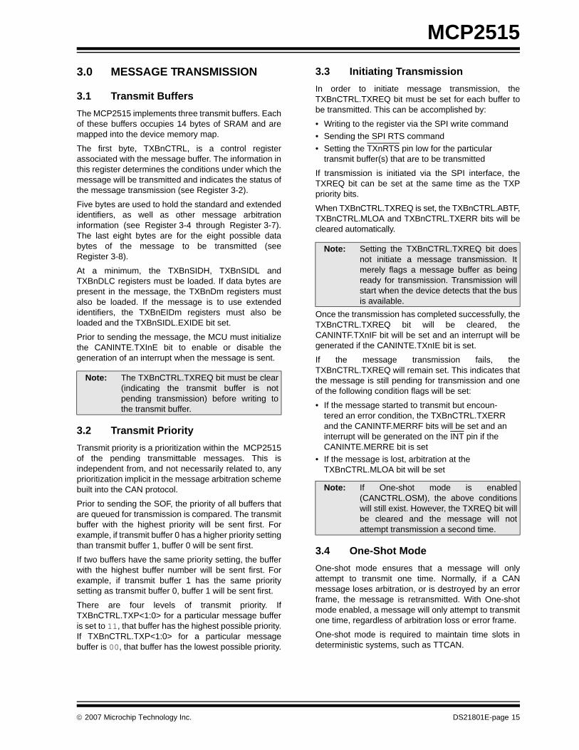
REGISTER 3-4: TXBnSIDL – TRANSMIT BUFFER n STANDARD IDENTIFIER LOW(ADDRESS: 32h, 42h, 52h)
R/W-x R/W-x R/W-x R/W-x R/W-x R/W-x R/W-x R/W-xSID2 SID1 SID0 — EXIDE — EID17 EID16
bit 7 bit 0
Legend:R = Readable bit W = Writable bit U = Unimplemented bit, read as ‘0’-n = Value at POR ‘1’ = Bit is set ‘0’ = Bit is cleared x = Bit is unknown
bit 7-5 SID: Standard Identifier bits <2:0>bit 4 Unimplemented: Reads as ‘0’bit 3 EXIDE: Extended Identifier Enable bit
1 = Message will transmit extended identifier0 = Message will transmit standard identifier
bit 2 Unimplemented: Reads as ‘0’bit 1-0 EID: Extended Identifier bits <17:16>
REGISTER 3-5: TXBnEID8 – TRANSMIT BUFFER n EXTENDED IDENTIFIER HIGH(ADDRESS: 33h, 43h, 53h)
R/W-x R/W-x R/W-x R/W-x R/W-x R/W-x R/W-x R/W-xEID15 EID14 EID13 EID12 EID11 EID10 EID9 EID8
bit 7 bit 0
Legend:R = Readable bit W = Writable bit U = Unimplemented bit, read as ‘0’-n = Value at POR ‘1’ = Bit is set ‘0’ = Bit is cleared x = Bit is unknown
bit 7-0 EID: Extended Identifier bits <15:8>
REGISTER 3-6: TXBnEID0 – TRANSMIT BUFFER n EXTENDED IDENTIFIER LOW(ADDRESS: 34h, 44h, 54h)
R/W-x R/W-x R/W-x R/W-x R/W-x R/W-x R/W-x R/W-xEID7 EID6 EID5 EID4 EID3 EID2 EID1 EID0
bit 7 bit 0
Legend:R = Readable bit W = Writable bit U = Unimplemented bit, read as ‘0’-n = Value at POR ‘1’ = Bit is set ‘0’ = Bit is cleared x = Bit is unknown
bit 7-0 EID: Extended Identifier bits <7:0>
DS21801E-page 20 © 2007 Microchip Technology Inc.

MCP2515
M
REGISTER 3-7: TXBnDLC - TRANSMIT BUFFER n DATA LENGTH CODE(ADDRESS: 35h, 45h, 55h)
R/W-x R/W-x R/W-x R/W-x R/W-x R/W-x R/W-x R/W-x— RTR — — DLC3 DLC2 DLC1 DLC0
bit 7 bit 0
Legend:R = Readable bit W = Writable bit U = Unimplemented bit, read as ‘0’-n = Value at POR ‘1’ = Bit is set ‘0’ = Bit is cleared x = Bit is unknown
bit 7 Unimplemented: Reads as ‘0’bit 6 RTR: Remote Transmission Request bit
1 = Transmitted Message will be a Remote Transmit Request0 = Transmitted Message will be a Data Frame
bit 5-4 Unimplemented: Reads as ‘0’bit 3-0 DLC: Data Length Code <3:0> bits
Sets the number of data bytes to be transmitted (0 to 8 bytes)
Note: It is possible to set the DLC to a value greater than 8, however only 8 bytes are transmitted
REGISTER 3-8: TXBnDm – TRANSMIT BUFFER n DATA BYTE m(ADDRESS: 36h - 3Dh, 46h - 4Dh, 56h - 5Dh)
R/W-x R/W-x R/W-x R/W-x R/W-x R/W-x R/W-x R/W-xTXBnDm7 TXBnDm6 TXBnDm5 TXBnDm4 TXBnDm3 TXBnDm2 TXBnDm1 TXBnDm0
bit 7 bit 0
Legend:R = Readable bit W = Writable bit U = Unimplemented bit, read as ‘0’-n = Value at POR ‘1’ = Bit is set ‘0’ = Bit is cleared x = Bit is unknown
bit 7-0 TXBnDM7:TXBnDM0: Transmit Buffer n Data Field Bytes m
© 2007 Microchip Technology Inc. DS21801E-page 21

MCP2515
NOTES:DS21801E-page 22 © 2007 Microchip Technology Inc.

MCP2515
4.0 MESSAGE RECEPTION
4.1 Receive Message BufferingThe MCP2515 includes two full receive buffers withmultiple acceptance filters for each. There is also aseparate Message Assembly Buffer (MAB) that acts asa third receive buffer (see Figure 4-2).
4.1.1 MESSAGE ASSEMBLY BUFFEROf the three receive buffers, the MAB is alwayscommitted to receiving the next message from the bus.The MAB assembles all messages received. Thesemessages will be transferred to the RXBn buffers (SeeRegister 4-4 to Register 4-9) only if the acceptancefilter criteria is met.
4.1.2 RXB0 AND RXB1The remaining two receive buffers, called RXB0 andRXB1, can receive a complete message from theprotocol engine via the MAB. The MCU can access onebuffer, while the other buffer is available for messagereception, or for holding a previously receivedmessage.
4.1.3 RECEIVE FLAGS/INTERRUPTSWhen a message is moved into either of the receivebuffers, the appropriate CANINTF.RXnIF bit is set. Thisbit must be cleared by the MCU in order to allow a newmessage to be received into the buffer. This bitprovides a positive lockout to ensure that the MCU hasfinished with the message before the MCP2515attempts to load a new message into the receive buffer.
If the CANINTE.RXnIE bit is set, an interrupt will begenerated on the INT pin to indicate that a validmessage has been received. In addition, theassociated RXnBF pin will drive low if configured as areceive buffer full pin. See Section 4.4 “RX0BF andRX1BF Pins” for details.
4.2 Receive PriorityRXB0, the higher priority buffer, has one mask and twomessage acceptance filters associated with it. Thereceived message is applied to the mask and filters forRXB0 first.
RXB1 is the lower priority buffer, with one mask andfour acceptance filters associated with it.
In addition to the message being applied to the RB0mask and filters first, the lower number of acceptancefilters makes the match on RXB0 more restrictive andimplies a higher priority for that buffer.
When a message is received, bits <3:0> of theRXBnCTRL register will indicate the acceptance filternumber that enabled reception and whether thereceived message is a remote transfer request.
4.2.1 ROLLOVERAdditionally, the RXB0CTRL register can be configuredsuch that, if RXB0 contains a valid message andanother valid message is received, an overflow errorwill not occur and the new message will be moved intoRXB1, regardless of the acceptance criteria of RXB1.
4.2.2 RXM BITSThe RXBnCTRL.RXM bits set special receive modes.Normally, these bits are cleared to 00 to enablereception of all valid messages as determined by theappropriate acceptance filters. In this case, thedetermination of whether or not to receive standard orextended messages is determined by theRFXnSIDL.EXIDE bit in the acceptance filter register.
If the RXBnCTRL.RXM bits are set to 01 or 10, thereceiver will only accept messages with standard orextended identifiers, respectively. If an acceptancefilter has the RFXnSIDL.EXIDE bit set such that it doesnot correspond with the RXBnCTRL.RXM mode, thatacceptance filter is rendered useless. These twomodes of RXBnCTRL.RXM bits can be used insystems where it is known that only standard orextended messages will be on the bus.
If the RXBnCTRL.RXM bits are set to 11, the buffer willreceive all messages, regardless of the values of theacceptance filters. Also, if a message has an errorbefore the EOF, that portion of the message assembledin the MAB before the error frame will be loaded into thebuffer. This mode has some value in debugging a CANsystem and would not be used in an actual systemenvironment.
Note: The entire contents of the MAB is movedinto the receive buffer once a message isaccepted. This means that, regardless ofthe type of identifier (standard orextended) and the number of data bytesreceived, the entire receive buffer isoverwritten with the MAB contents.Therefore, the contents of all registers inthe buffer must be assumed to have beenmodified when any message is received.
© 2007 Microchip Technology Inc. DS21801E-page 23
MCP2515
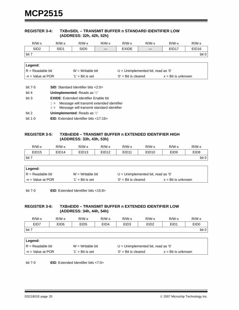
4.3 Start-of-Frame SignalIf enabled, the Start-Of-Frame signal is generated onthe SOF pin at the beginning of each CAN messagedetected on the RXCAN pin.The RXCAN pin monitors an idle bus for a recessive-to-dominant edge. If the dominant condition remainsuntil the sample point, the DSTEMP interprets this as aSOF and a SOF pulse is generated. If the dominantcondition does not remain until the sample point, theDSTEMP interprets this as a glitch on the bus and noSOF signal is generated. Figure 4-1 illustrates SOFsignalling and glitch-filtering.
As with One-shot mode, one use for SOF signaling isfor TTCAN-type systems. In addition, by monitoringboth the RXCAN pin and the SOF pin, a MCU candetect early physical bus problems by detecting smallglitches before they affect the CAN communications.
4.4 RX0BF and RX1BF PinsIn addition to the INT pin, which provides an interruptsignal to the MCU for many different conditions, thereceive buffer full pins (RX0BF and RX1BF) can beused to indicate that a valid message has been loadedinto RXB0 or RXB1, respectively. The pins have threedifferent configurations (Register 4-1):
1. Disabled.2. Buffer Full Interrupt.3. Digital Output.
4.4.1 DISABLEDThe RXBnBF pins can be disabled to the high-impedance state by clearing BFPCTRL.BnBFE.
4.4.2 CONFIGURED AS BUFFER FULLThe RXBnBF pins can be configured to act as eitherbuffer full interrupt pins or as standard digital outputs.Configuration and status of these pins is available viathe BFPCTRL register (Register 4-3). When set tooperate in Interrupt mode (by setting BFPCTRL.BxBFEand BFPCTRL.BxBFM bits), these pins are active-lowand are mapped to the CANINTF.RXnIF bit for eachreceive buffer. When this bit goes high for one of thereceive buffers (indicating that a valid message hasbeen loaded into the buffer), the correspondingRXBnBF pin will go low. When the CANINTF.RXnIF bitis cleared by the MCU, the corresponding interrupt pinwill go to the logic-high state until the next message isloaded into the receive buffer.
FIGURE 4-1: START-OF-FRAME SIGNALING
START-OF-FRAME BIT
SamplePoint
ID BIT
RXCAN
SOF
EXPECTED START-OF-FRAME BIT
SamplePoint BUS IDLE
RXCAN
SOF
Expected
Normal SOF Signaling
Glitch-Filtering
DS21801E-page 24 © 2007 Microchip Technology Inc.

MCP2515
4.4.3 CONFIGURED AS DIGITAL OUTPUTWhen used as digital outputs, the BFPCTRL.BxBFM bitmust be cleared and BFPCTRL.BnBFE must be set forthe associated buffer. In this mode, the state of the pinis controlled by the BFPCTRL.BnBFS bits. Writing a ‘1’to the BnBFS bit will cause a high level to be driven onthe associated buffer full pin, while a ‘0’ will cause thepin to drive low. When using the pins in this mode, thestate of the pin should be modified only by using the BitModify SPI command to prevent glitches fromoccurring on either of the buffer full pins.TABLE 4-1: CONFIGURING RXNBF PINS
FIGURE 4-2: RECEIVE BUFFER BLOCK DIAGRAM
BnBFE BnBFM BnBFS Pin Status
0 X X Disabled, high-impedance1 1 X Receive buffer interrupt1 0 0 Digital output = 01 0 1 Digital output = 1
Acceptance MaskRXM1
Acceptance FilterRXF2
Acceptance FilterRXF3
Acceptance FilterRXF4
Acceptance FilterRXF5
Acceptance MaskRXM0
Acceptance FilterRXF0
Acceptance FilterRXF1
Identifier
Data Field Data Field
Identifier
Note: Messages received in the MAB are intiallyapplied to the mask and filters of RXB0. Inaddition, only one filter match occurs (e.g.,if the message matches both RXF0 andRXF2, the match will be for RXF0 and themessage will be moved into RXB0).
Accept
Accept
RXB0
RXB1
MAB
© 2007 Microchip Technology Inc. DS21801E-page 25

MCP2515
FIGURE 4-3: RECEIVE FLOW FLOWCHARTSet RXBF0
Start
DetectStart of
Message?
ValidMessage
Received?
GenerateError
Meetsa filter criteria
IsCANINTF.RX0IF = 0?
Go to Start
Move message into RXB0
Set RXB0CTRL.FILHIT <2:0>
IsCANINTF.RX1IF = 0?
Move message into RXB1
Set CANINTF.RX1IF = 1
Yes
No
GenerateInterrupt on INT
Yes Yes
No No
Yes
Yes
No
No
Yes
Yes
Frame
No Yes
No
Begin Loading Message intoMessage Assembly Buffer (MAB)
according to which filter criteriawas met
Set RXB0CTRL.FILHIT <0>according to which filter criteria
Set CANSTAT <3:0> accord-ing to which receive buffer the message was loaded into
IsRXB0CTRL.BUKT = 1?
Generate Overflow Error:Set EFLG.RX1OVR
IsCANINTE.ERRIE = 1?
No
Go to Start
Yes
No
AreBFPCTRL.B0BFM = 1
BF1CTRL.B0BFE = 1?and Pin = 0
No
Set RXBF1Pin = 0
No
YesYes
CANINTE.RX0IE = 1? CANINTE.RX1IE = 1?
RXB1RXB0
Set EFLG.RX0OVRGenerate Overflow Error:
Set CANINTF.RX0IF = 1
AreBFPCTRL.B1BFM = 1
BF1CTRL.B1BFE = 1?and
Meetsa filter criteria
for RXB1?for RXB0?No Yes
GenerateInterrupt on INT
Determines if the receiveregister is empty and ableto accept a new message
Determines if RXB0 can rollover into RXB1, if it is full.
DS21801E-page 26 © 2007 Microchip Technology Inc.

MCP2515
REGISTER 4-1: RXB0CTRL – RECEIVE BUFFER 0 CONTROL(ADDRESS: 60h)
U-0 R/W-0 R/W-0 U-0 R-0 R/W-0 R-0 R-0— RXM1 RXM0 — RXRTR BUKT BUKT1 FILHIT0
bit 7 bit 0
Legend:R = Readable bit W = Writable bit U = Unimplemented bit, read as ‘0’-n = Value at POR ‘1’ = Bit is set ‘0’ = Bit is cleared x = Bit is unknown
bit 7 Unimplemented: Read as ‘0’bit 6-5 RXM: Receive Buffer Operating Mode bits
11 = Turn mask/filters off; receive any message10 = Receive only valid messages with extended identifiers that meet filter criteria01 = Receive only valid messages with standard identifiers that meet filter criteria00 = Receive all valid messages using either standard or extended identifiers that meet filter criteria
bit 4 Unimplemented: Read as ‘0’bit 3 RXRTR: Received Remote Transfer Request bit
1 = Remote Transfer Request Received0 = No Remote Transfer Request Received
bit 2 BUKT: Rollover Enable bit1 = RXB0 message will rollover and be written to RXB1 if RXB0 is full0 = Rollover disabled
bit 1 BUKT1: Read-only Copy of BUKT bit (used internally by the MCP2515)bit 0 FILHIT: Filter Hit bit - indicates which acceptance filter enabled reception of message
1 = Acceptance Filter 1 (RXF1)0 = Acceptance Filter 0 (RXF0)
Note: If a rollover from RXB0 to RXB1 occurs, the FILHIT bit will reflect the filter that acceptedthe message that rolled over.
© 2007 Microchip Technology Inc. DS21801E-page 27

MCP2515
REGISTER 4-2: RXB1CTRL – RECEIVE BUFFER 1 CONTROL(ADDRESS: 70h)
U-0 R/W-0 R/W-0 U-0 R-0 R-0 R-0 R-0— RXM1 RXM0 — RXRTR FILHIT2 FILHIT1 FILHIT0
bit 7 bit 0
Legend:R = Readable bit W = Writable bit U = Unimplemented bit, read as ‘0’-n = Value at POR ‘1’ = Bit is set ‘0’ = Bit is cleared x = Bit is unknown
bit 7 Unimplemented: Read as ‘0’bit 6-5 RXM: Receive Buffer Operating Mode bits
11 = Turn mask/filters off; receive any message10 = Receive only valid messages with extended identifiers that meet filter criteria01 = Receive only valid messages with standard identifiers that meet filter criteria00 = Receive all valid messages using either standard or extended identifiers that meet filter criteria
bit 4 Unimplemented: Read as ‘0’bit 3 RXRTR: Received Remote Transfer Request bit
1 = Remote Transfer Request Received0 = No Remote Transfer Request Received
bit 2-0 FILHIT: Filter Hit bits - indicates which acceptance filter enabled reception of message101 = Acceptance Filter 5 (RXF5)100 = Acceptance Filter 4 (RXF4)011 = Acceptance Filter 3 (RXF3)010 = Acceptance Filter 2 (RXF2)001 = Acceptance Filter 1 (RXF1) (Only if BUKT bit set in RXB0CTRL)000 = Acceptance Filter 0 (RXF0) (Only if BUKT bit set in RXB0CTRL)
DS21801E-page 28 © 2007 Microchip Technology Inc.

MCP2515
REGISTER 4-3: BFPCTRL – RXnBF PIN CONTROL AND STATUS(ADDRESS: 0Ch)
U-0 U-0 R/W-0 R/W-0 R/W-0 R/W-0 R/W-0 R/W-0— — B1BFS B0BFS B1BFE B0BFE B1BFM B0BFM
bit 7 bit 0
Legend:R = Readable bit W = Writable bit U = Unimplemented bit, read as ‘0’-n = Value at POR ‘1’ = Bit is set ‘0’ = Bit is cleared x = Bit is unknown
bit 7 Unimplemented: Read as ‘0’bit 6 Unimplemented: Read as ‘0’bit 5 B1BFS: RX1BF Pin State bit (Digital Output mode only)
- Reads as ‘0’ when RX1BF is configured as interrupt pinbit 4 B0BFS: RX0BF Pin State bit (Digital Output mode only)
- Reads as ‘0’ when RX0BF is configured as interrupt pinbit 3 B1BFE: RX1BF Pin Function Enable bit
1 = Pin function enabled, operation mode determined by B1BFM bit0 = Pin function disabled, pin goes to high-impedance state
bit 2 B0BFE: RX0BF Pin Function Enable bit1 = Pin function enabled, operation mode determined by B0BFM bit0 = Pin function disabled, pin goes to high-impedance state
bit 1 B1BFM: RX1BF Pin Operation Mode bit1 = Pin is used as interrupt when valid message loaded into RXB10 = Digital Output mode
bit 0 B0BFM: RX0BF Pin Operation Mode bit1 = Pin is used as interrupt when valid message loaded into RXB00 = Digital Output mode
REGISTER 4-4: RXBnSIDH – RECEIVE BUFFER n STANDARD IDENTIFIER HIGH(ADDRESS: 61h, 71h)
R-x R-x R-x R-x R-x R-x R-x R-xSID10 SID9 SID8 SID7 SID6 SID5 SID4 SID3
bit 7 bit 0
Legend:R = Readable bit W = Writable bit U = Unimplemented bit, read as ‘0’-n = Value at POR ‘1’ = Bit is set ‘0’ = Bit is cleared x = Bit is unknown
bit 7-0 SID: Standard Identifier bits <10:3>These bits contain the eight most significant bits of the Standard Identifier for the received message
© 2007 Microchip Technology Inc. DS21801E-page 29

MCP2515
REGISTER 4-5: RXBnSIDL – RECEIVE BUFFER n STANDARD IDENTIFIER LOW(ADDRESS: 62h, 72h)
R-x R-x R-x R-x R-x U-0 R-x R-xSID2 SID1 SID0 SRR IDE — EID17 EID16
bit 7 bit 0
Legend:R = Readable bit W = Writable bit U = Unimplemented bit, read as ‘0’-n = Value at POR ‘1’ = Bit is set ‘0’ = Bit is cleared x = Bit is unknown
bit 7-5 SID: Standard Identifier bits <2:0>These bits contain the three least significant bits of the Standard Identifier for the received message
bit 4 SRR: Standard Frame Remote Transmit Request bit (valid only if IDE bit = ‘0’)1 = Standard Frame Remote Transmit Request Received0 = Standard Data Frame Received
bit 3 IDE: Extended Identifier Flag bitThis bit indicates whether the received message was a Standard or an Extended Frame1 = Received message was an Extended Frame0 = Received message was a Standard Frame
bit 2 Unimplemented: Reads as ‘0’bit 1-0 EID: Extended Identifier bits <17:16>
These bits contain the two most significant bits of the Extended Identifier for the received message
REGISTER 4-6: RXBnEID8 – RECEIVE BUFFER n EXTENDED IDENTIFIER HIGH(ADDRESS: 63h, 73h)
R-x R-x R-x R-x R-x R-x R-x R-xEID15 EID14 EID13 EID12 EID11 EID10 EID9 EID8
bit 7 bit 0
Legend:R = Readable bit W = Writable bit U = Unimplemented bit, read as ‘0’-n = Value at POR ‘1’ = Bit is set ‘0’ = Bit is cleared x = Bit is unknown
bit 7-0 EID: Extended Identifier bits <15:8>These bits hold bits 15 through 8 of the Extended Identifier for the received message
DS21801E-page 30 © 2007 Microchip Technology Inc.

MCP2515
REGISTER 4-7: RXBnEID0 – RECEIVE BUFFER n EXTENDED IDENTIFIER LOW(ADDRESS: 64h, 74h)
R-x R-x R-x R-x R-x R-x R-x R-xEID7 EID6 EID5 EID4 EID3 EID2 EID1 EID0
bit 7 bit 0
Legend:R = Readable bit W = Writable bit U = Unimplemented bit, read as ‘0’-n = Value at POR ‘1’ = Bit is set ‘0’ = Bit is cleared x = Bit is unknown
bit 7-0 EID: Extended Identifier bits <7:0>These bits hold the least significant eight bits of the Extended Identifier for the received message
REGISTER 4-8: RXBnDLC – RECEIVE BUFFER n DATA LENGHT CODE(ADDRESS: 65h, 75h)
R-x R-x R-x R-x R-x R-x R-x R-xEID7 EID6 EID5 EID4 EID3 EID2 EID1 EID0
bit 7 bit 0
Legend:R = Readable bit W = Writable bit U = Unimplemented bit, read as ‘0’-n = Value at POR ‘1’ = Bit is set ‘0’ = Bit is cleared x = Bit is unknown
bit 7 Unimplemented: Reads as ‘0’bit 6 RTR: Extended Frame Remote Transmission Request bit
(valid only when RXBnSIDL.IDE = ‘1’)1 = Extended Frame Remote Transmit Request Received0 = Extended Data Frame Received
bit 5 RB1: Reserved Bit 1bit 4 RB0: Reserved Bit 0bit 3-0 DLC: Data Length Code bits <3:0>
Indicates number of data bytes that were received
REGISTER 4-9: RXBnDM – RECEIVE BUFFER n DATA BYTE M(ADDRESS: 66h - 6Dh, 76h - 7Dh)
R-x R-x R-x R-x R-x R-x R-x R-xRBnDm7 RBnDm6 RBnDm5 RBnDm4 RBnDm3 RBnDm2 RBnDm1 RBnDm0
bit 7 bit 0
Legend:R = Readable bit W = Writable bit U = Unimplemented bit, read as ‘0’-n = Value at POR ‘1’ = Bit is set ‘0’ = Bit is cleared x = Bit is unknown
bit 7-0 RBnDm7:RBnDm0: Receive Buffer n Data Field Bytes mEight bytes containing the data bytes for the received message
© 2007 Microchip Technology Inc. DS21801E-page 31
MCP2515
4.5 Message Acceptance Filters andMasksThe message acceptance filters and masks are used todetermine if a message in the message assemblybuffer should be loaded into either of the receivebuffers (see Figure 4-5). Once a valid message hasbeen received into the MAB, the identifier fields of themessage are compared to the filter values. If there is amatch, that message will be loaded into the appropriatereceive buffer.
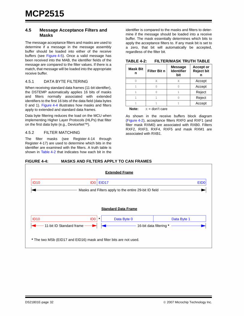
4.5.1 DATA BYTE FILTERINGWhen receiving standard data frames (11-bit identifier),the DSTEMP automatically applies 16 bits of masksand filters normally associated with extendedidentifiers to the first 16 bits of the data field (data bytes0 and 1). Figure 4-4 illustrates how masks and filtersapply to extended and standard data frames.
Data byte filtering reduces the load on the MCU whenimplementing Higher Layer Protocols (HLPs) that filteron the first data byte (e.g., DeviceNet™).
4.5.2 FILTER MATCHINGThe filter masks (see Register 4-14 throughRegister 4-17) are used to determine which bits in theidentifier are examined with the filters. A truth table isshown in Table 4-2 that indicates how each bit in the
identifier is compared to the masks and filters to deter-mine if the message should be loaded into a receivebuffer. The mask essentially determines which bits toapply the acceptance filters to. If any mask bit is set toa zero, that bit will automatically be accepted,regardless of the filter bit.
TABLE 4-2: FILTER/MASK TRUTH TABLE
As shown in the receive buffers block diagram(Figure 4-2), acceptance filters RXF0 and RXF1 (andfilter mask RXM0) are associated with RXB0. FiltersRXF2, RXF3, RXF4, RXF5 and mask RXM1 areassociated with RXB1.
FIGURE 4-4: MASKS AND FILTERS APPLY TO CAN FRAMES
Mask Bit n Filter Bit n
Message Identifier
bit
Accept or Reject bit
n0 X X Accept1 0 0 Accept1 0 1 Reject1 1 0 Reject1 1 1 Accept
Note: X = don’t care
Extended Frame
Standard Data Frame
ID10 ID0 EID17 EID0
Masks and Filters apply to the entire 29-bit ID field
ID10 ID0 Data Byte 0 Data Byte 1
11-bit ID Standard frame
*
16-bit data filtering *
* The two MSb (EID17 and EID16) mask and filter bits are not used.
DS21801E-page 32 © 2007 Microchip Technology Inc.

MCP2515
4.5.3 FILHIT BITSFilter matches on received messages can bedetermined by the FILHIT bits in the associatedRXBnCTRL register. RXB0CTRL.FILHIT0 for buffer 0and RXB1CTRL.FILHIT<2:0> for buffer 1.The three FILHIT bits for receive buffer 1 (RXB1) arecoded as follows:
- 101 = Acceptance Filter 5 (RXF5)- 100 = Acceptance Filter 4 (RXF4)- 011 = Acceptance Filter 3 (RXF3)- 010 = Acceptance Filter 2 (RXF2)- 001 = Acceptance Filter 1 (RXF1) - 000 = Acceptance Filter 0 (RXF0)
RXB0CTRL contains two copies of the BUKT bit andthe FILHIT<0> bit.
The coding of the BUKT bit enables these three bits tobe used similarly to the RXB1CTRL.FILHIT bits and todistinguish a hit on filter RXF0 and RXF1 in eitherRXB0 or after a roll over into RXB1.
- 111 = Acceptance Filter 1 (RXB1)- 110 = Acceptance Filter 0 (RXB1)- 001 = Acceptance Filter 1 (RXB0)- 000 = Acceptance Filter 0 (RXB0)
If the BUKT bit is clear, there are six codescorresponding to the six filters. If the BUKT bit is set,there are six codes corresponding to the six filters, plustwo additional codes corresponding to RXF0 and RXF1filters that roll over into RXB1.
4.5.4 MULTIPLE FILTER MATCHESIf more than one acceptance filter matches, the FILHITbits will encode the binary value of the lowestnumbered filter that matched. For example, if filterRXF2 and filter RXF4 match, FILHIT will be loaded withthe value for RXF2. This essentially prioritizes theacceptance filters with a lower-numbered filter havinghigher priority. Messages are compared to filters inascending order of filter number. This also insures thatthe message will only be received into one buffer. Thisimplies that RXB0 has a higher priority than RXB1.
4.5.5 CONFIGURING THE MASKS AND FILTERS
The mask and filter registers can only be modifiedwhen the MCP2515 is in Configuration mode (seeSection 10.0 “Modes of Operation”).
FIGURE 4-5: MESSAGE ACCEPTANCE MASK AND FILTER OPERATION
Note: 000 and 001 can only occur if the BUKT bitin RXB0CTRL is set, allowing RXB0messages to roll over into RXB1.
Acceptance Filter Register Acceptance Mask Register
RxRqst
Message Assembly Buffer
RXFn0
RXFn1
RXFnn
RXMn0
RXMn1
RXMnn
Identifier
© 2007 Microchip Technology Inc. DS21801E-page 33

MCP2515
REGISTER 4-10: RXFnSIDH – FILTER n STANDARD IDENTIFIER HIGH(ADDRESS: 00h, 04h, 08h, 10h, 14h, 18h)
R/W-x R/W-x R/W-x R/W-x R/W-x R/W-x R/W-x R/W-xSID10 SID9 SID8 SID7 SID6 SID5 SID4 SID3
bit 7 bit 0
Legend:R = Readable bit W = Writable bit U = Unimplemented bit, read as ‘0’-n = Value at POR ‘1’ = Bit is set ‘0’ = Bit is cleared x = Bit is unknown
bit 7-0 SID: Standard Identifier Filter bits <10:3>These bits hold the filter bits to be applied to bits <10:3> of the Standard Identifier portion of a receivedmessage
REGISTER 4-11: RXFnSIDL – FILTER n STANDARD IDENTIFIER LOW(ADDRESS: 01h, 05h, 09h, 11h, 15h, 19h)
R/W-x R/W-x R/W-x U-0 R/W-x U-0 R/W-x R/W-xSID2 SID1 SID0 — EXIDE — EID17 EID16
bit 7 bit 0
Legend:R = Readable bit W = Writable bit U = Unimplemented bit, read as ‘0’-n = Value at POR ‘1’ = Bit is set ‘0’ = Bit is cleared x = Bit is unknown
bit 7-5 SID: Standard Identifier Filter bits <2:0>These bits hold the filter bits to be applied to bits <2:0> of the Standard Identifier portion of a receivedmessage
bit 4 Unimplemented: Reads as ‘0’bit 3 EXIDE: Extended Identifier Enable bit
1 = Filter is applied only to Extended Frames0 = Filter is applied only to Standard Frames
bit 2 Unimplemented: Reads as ‘0’bit 1-0 EID: Extended Identifier Filter bits <17:16>
These bits hold the filter bits to be applied to bits <17:16> of the Extended Identifier portion of areceived message
DS21801E-page 34 © 2007 Microchip Technology Inc.

MCP2515
REGISTER 4-12: RXFnEID8 – FILTER n EXTENDED IDENTIFIER HIGH(ADDRESS: 02h, 06h, 0Ah, 12h, 16h, 1Ah)
R/W-x R/W-x R/W-x R/W-x R/W-x R/W-x R/W-x R/W-xEID15 EID14 EID13 EID12 EID11 EID10 EID9 EID8
bit 7 bit 0
Legend:R = Readable bit W = Writable bit U = Unimplemented bit, read as ‘0’-n = Value at POR ‘1’ = Bit is set ‘0’ = Bit is cleared x = Bit is unknown
bit 7-0 EID: Extended Identifier bits <15:8>These bits hold the filter bits to be applied to bits <15:8> of the Extended Identifier portion of a receivedmessage
REGISTER 4-13: RXFnEID0 – FILTER n EXTENDED IDENTIFIER LOW(ADDRESS: 03h, 07h, 0Bh, 13h, 17h, 1Bh)
R/W-x R/W-x R/W-x R/W-x R/W-x R/W-x R/W-x R/W-xEID7 EID6 EID5 EID4 EID3 EID2 EID1 EID0
bit 7 bit 0
Legend:R = Readable bit W = Writable bit U = Unimplemented bit, read as ‘0’-n = Value at POR ‘1’ = Bit is set ‘0’ = Bit is cleared x = Bit is unknown
bit 7-0 EID: Extended Identifier bits <7:0>These bits hold the filter bits to be applied to the bits <7:0> of the Extended Identifier portion of areceived message
REGISTER 4-14: RXMnSIDH – MASK n STANDARD IDENTIFIER HIGH(ADDRESS: 20h, 24h)
R/W-0 R/W-0 R/W-0 R/W-0 R/W-0 R/W-0 R/W-0 R/W-0SID10 SID9 SID8 SID7 SID6 SID5 SID4 SID3
bit 7 bit 0
Legend:R = Readable bit W = Writable bit U = Unimplemented bit, read as ‘0’-n = Value at POR ‘1’ = Bit is set ‘0’ = Bit is cleared x = Bit is unknown
bit 7-0 SID: Standard Identifier Mask bits <10:3>These bits hold the mask bits to be applied to bits <10:3> of the Standard Identifier portion of a receivedmessage
© 2007 Microchip Technology Inc. DS21801E-page 35

MCP2515
\
REGISTER 4-15: RXMnSIDL – MASK n STANDARD IDENTIFIER LOW(ADDRESS: 21h, 25h)
R/W-0 R/W-0 R/W-0 U-0 U-0 U-0 R/W-0 R/W-0SID2 SID1 SID0 — — — EID17 EID16
bit 7 bit 0
Legend:R = Readable bit W = Writable bit U = Unimplemented bit, read as ‘0’-n = Value at POR ‘1’ = Bit is set ‘0’ = Bit is cleared x = Bit is unknown
bit 7-5 SID: Standard Identifier Mask bits <2:0>These bits hold the mask bits to be applied to bits<2:0> of the Standard Identifier portion of a receivedmessage
bit 4-2 Unimplemented: Reads as ‘0’bit 1-0 EID: Extended Identifier Mask bits <17:16>
These bits hold the mask bits to be applied to bits <17:16> of the Extended Identifier portion of areceived message
REGISTER 4-16: RXMnEID8 – MASK n EXTENDED IDENTIFIER HIGH(ADDRESS: 22h, 26h)
R/W-0 R/W-0 R/W-0 R/W-0 R/W-0 R/W-0 R/W-0 R/W-0EID15 EID14 EID13 EID12 EID11 EID10 EID9 EID8
bit 7 bit 0
Legend:R = Readable bit W = Writable bit U = Unimplemented bit, read as ‘0’-n = Value at POR ‘1’ = Bit is set ‘0’ = Bit is cleared x = Bit is unknown
bit 7-0 EID: Extended Identifier bits <15:8>These bits hold the filter bits to be applied to bits <15:8> of the Extended Identifier portion of a receivedmessage
REGISTER 4-17: RXMnEID0 – MASK n EXTENDED IDENTIFIER LOW(ADDRESS: 23h, 27h)
R/W-0 R/W-0 R/W-0 R/W-0 R/W-0 R/W-0 R/W-0 R/W-0EID7 EID6 EID5 EID4 EID3 EID2 EID1 EID0
bit 7 bit 0
Legend:R = Readable bit W = Writable bit U = Unimplemented bit, read as ‘0’-n = Value at POR ‘1’ = Bit is set ‘0’ = Bit is cleared x = Bit is unknown
bit 7-0 EID: Extended Identifier Mask bits <7:0>These bits hold the mask bits to be applied to the bits <7:0> of the Extended Identifier portion of areceived message
DS21801E-page 36 © 2007 Microchip Technology Inc.

MCP2515
5.0 BIT TIMINGAll nodes on a given CAN bus must have the samenominal bit rate. The CAN protocol uses Non Return toZero (NRZ) coding, which does not encode a clockwithin the data stream. Therefore, the receive clockmust be recovered by the receiving nodes andsynchronized to the transmitter’s clock.
As oscillators and transmission times may vary fromnode to node, the receiver must have some type ofPhase Lock Loop (PLL) synchronized to datatransmission edges to synchronize and maintain thereceiver clock. Since the data is NRZ-coded, it isnecessary to include bit-stuffing to insure that an edgeoccurs at least every six bit times to maintain the DigitalPhase Lock Loop (DPLL) synchronization.
The bit timing of the MCP2515 is implemented using aDPLL that is configured to synchronize to the incomingdata, as well as provide the nominal timing for thetransmitted data. The DPLL breaks each bit time intomultiple segments made up of minimal periods of time,called the Time Quanta (TQ).
Bus timing functions executed within the bit time frame(such as synchronization to the local oscillator, networktransmission delay compensation and sample pointpositioning) are defined by the programmable bit timinglogic of the DPLL.
5.1 The CAN Bit TImeAll devices on the CAN bus must use the same bit rate.However, all devices are not required to have the samemaster oscillator clock frequency. For the differentclock frequencies of the individual devices, the bit ratehas to be adjusted by appropriately setting the baudrate prescaler and number of time quanta in eachsegment.
The CAN bit time is made up of non-overlappingsegments. Each of these segments are made up ofinteger units called Time Quanta (TQ), explained laterin this data sheet. The Nominal Bit Rate (NBR) isdefined in the CAN specification as the number of bitsper second transmitted by an ideal transmitter with noresynchronization. It can be described with theequation:
EQUATION 5-1:
Nominal Bit TimeThe Nominal Bit Time (NBT) (tbit) is made up of non-overlapping segments (Figure 5-1). Therefore, theNBT is the summation of the following segments:
Associated with the NBT are the sample point,Synchronization Jump Width (SJW) and InformationProcessing Time (IPT), which are explained later.
SYNCHRONIZATION SEGMENTThe Synchronization Segment (SyncSeg) is the firstsegment in the NBT and is used to synchronize thenodes on the bus. Bit edges are expected to occurwithin the SyncSeg. This segment is fixed at 1 TQ.
FIGURE 5-1: CAN BIT TIME SEGMENTS
NBR fbit1
tbit-------= =
tbit tSyncSeg tPropSeg tPS1 tPS2+ + +=
Nominal Bit Time (NBT), tbit
SamplePoint
SyncSeg PropSeg PhaseSeg1 (PS1) PhaseSeg2 (PS2)
© 2007 Microchip Technology Inc. DS21801E-page 37

MCP2515
PROPAGATION SEGMENTThe Propagation Segment (PropSeg) exists tocompensate for physical delays between nodes. Thepropagation delay is defined as twice the sum of thesignal’s propagation time on the bus line, including thedelays associated with the bus driver. The PropSeg isprogrammable from 1 – 8 TQ.PHASE SEGMENT 1 (PS1) AND PHASE SEGMENT 2 (PS2)The two phase segments, PS1 and PS2, are used tocompensate for edge phase errors on the bus. PS1 canbe lengthened (or PS2 shortened) by resyncronization.PS1 is programmable from 1 – 8 TQ and PS2 isprogrammable from 2 – 8 TQ.
SAMPLE POINTThe sample point is the point in the bit time at which thelogic level is read and interpreted. The sample point islocated at the end of PS1. The exception to this rule isif the sample mode is configured to sample three timesper bit. In this case, while the bit is still sampled at theend of PS1, two additional samples are taken at one-half TQ intervals prior to the end of PS1, with the valueof the bit being determined by a majority decision.
INFORMATION PROCESSING TIMEThe Information Processing Time (IPT) is the timerequired for the logic to determine the bit level of asampled bit. The IPT begins at the sample point, ismeasured in TQ and is fixed at 2 TQ for the MicrochipCAN module. Since PS2 also begins at the samplepoint and is the last segment in the bit time, it isrequired that the PS2 minimum is not less than the IPT.
Therefore:
SYNCHRONIZATION JUMP WIDTHThe Synchronization Jump Width (SJW) adjusts the bitclock as necessary by 1 – 4 TQ (as configured) tomaintain synchronization with the transmittedmessage. Synchronization is covered in more detaillater in this data sheet.
Time QuantumEach of the segments that make up a bit time are madeup of integer units called Time Quanta (TQ). The lengthof each Time Quantum is based on the oscillator period(tOSC). The base TQ equals twice the oscillator period.Figure 5-2 shows how the bit period is derived fromTOSC and TQ. The TQ length equals one TQ clockperiod (tBRPCLK), which is programmable using aprogrammable prescaler, called the Baud RatePrescaler (BRP). This is illustrated in the followingequation:
EQUATION 5-2:
FIGURE 5-2: TQ AND THE BIT PERIOD
PS2min IPT 2TQ= =
TQ 2 BRP TOSC⋅ ⋅ 2 BRP⋅FOSC-------------------= =
Where: BRP equals the configuration as shown inRegister 5-1.
tOSC
TBRPCLK
tBITSync(fixed)
PropSeg(Programmable)
PS2(Programmable)
PS1(Programmable)
TQ(tTQ)
CAN Bit Time
DS21801E-page 38 © 2007 Microchip Technology Inc.

MCP2515
5.2 SynchronizationTo compensate for phase shifts between the oscillatorfrequencies of each of the nodes on the bus, each CANcontroller must be able to synchronize to the relevantsignal edge of the incoming signal. Synchronization isthe process by which the DPLL function isimplemented.When an edge in the transmitted data is detected, thelogic will compare the location of the edge to theexpected time (SyncSeg). The circuit will then adjustthe values of PS1 and PS2 as necessary.
There are two mechanisms used for synchronization:
1. Hard synchronization.2. Resynchronization.
5.2.1 HARD SYNCHRONIZATIONHard synchronization is only performed when there is arecessive-to-dominant edge during a BUS IDLEcondition, indicating the start of a message. After hardsynchronization, the bit time counters are restarted withSyncSeg.
Hard synchronization forces the edge that hasoccurred to lie within the synchronization segment ofthe restarted bit time. Due to the rules ofsynchronization, if a hard synchronization occurs, therewill not be a resynchronization within that bit time.
5.2.2 RESYNCHRONIZATIONAs a result of resynchronization, PS1 may belengthened or PS2 may be shortened. The amount oflengthening or shortening of the phase buffer segmentshas an upper-bound, given by the SynchronizationJump Width (SJW).
The value of the SJW will be added to PS1 orsubtracted from PS2 (see Figure 5-3). The SJWrepresents the loop filtering of the DPLL. The SJW isprogrammable between 1 TQ and 4 TQ.
5.2.2.1 Phase ErrorsThe NRZ bit coding method does not encode a clockinto the message. Clocking information will only bederived from recessive-to-dominant transitions. Theproperty which states that only a fixed maximumnumber of successive bits have the same value (bit-stuffing) ensures resynchronization to the bit streamduring a frame.
The phase error of an edge is given by the position ofthe edge relative to SyncSeg, measured in TQ. Thephase error is defined in magnitude of TQ as follows:
• e = 0 if the edge lies within SYNCSEG.• e > 0 if the edge lies before the SAMPLE POINT
(TQ is added to PS1).• e < 0 if the edge lies after the SAMPLE POINT of
the previous bit (TQ is subtracted from PS2).
5.2.2.2 No Phase Error (e = 0)If the magnitude of the phase error is less than or equalto the programmed value of the SJW, the effect of aresynchronization is the same as that of a hardsynchronization.
5.2.2.3 Positive Phase Error (e > 0)If the magnitude of the phase error is larger than theSJW and, if the phase error is positive, PS1 islengthened by an amount equal to the SJW.
5.2.2.4 Negative Phase Error (e < 0)If the magnitude of the phase error is larger than theresynchronization jump width and the phase error isnegative, PS2 is shortened by an amount equal to theSJW.
5.2.3 SYNCHRONIZATION RULES1. Only recessive-to-dominant edges will be used
for synchronization.2. Only one synchronization within one bit time is
allowed.3. An edge will be used for synchronization only if
the value detected at the previous sample point(previously read bus value) differs from the busvalue immediately after the edge.
4. A transmitting node will not resynchronize on apositive phase error (e > 0).
5. If the absolute magnitude of the phase error isgreater than the SJW, the appropriate phasesegment will adjust by an amount equal to theSJW.
© 2007 Microchip Technology Inc. DS21801E-page 39

MCP2515
FIGURE 5-3: SYNCHRONIZING THE BIT TIMESyncSeg PropSeg PhaseSeg1 (PS1)PhaseSeg2 (PS2)
SamplePoint
SyncSeg PropSeg PhaseSeg1 (PS1)PhaseSeg2 (PS2)
SamplePoint
SyncSeg PropSeg PhaseSeg1 (PS1)PhaseSeg2 (PS2)
SamplePoint
Nominal Bit Time (NBT)
SJW (PS1)
SJW (PS2)
Nominal Bit Time (NBT)
SJW (PS1)
SJW (PS2)
Actual Bit Time
Resynchronization to a Slower Transmitter (e > 0)
Input Signal
Input Signal (e < 0)
SJW (PS1)
SJW (PS2)
Nominal Bit Time (NBT)
Actual Bit Time
Resynchronization to a Faster Transmitter (e < 0)
Input Signal (e = 0)
No Resynchronization (e = 0)
(e > 0)
DS21801E-page 40 © 2007 Microchip Technology Inc.
MCP2515
5.3 Programming Time SegmentsSome requirements for programming of the timesegments:• PropSeg + PS1 >= PS2• PropSeg + PS1 >= TDELAY
• PS2 > SJW
For example, assuming that a 125 kHz CAN baud ratewith FOSC = 20 MHz is desired:
TOSC = 50 ns, choose BRP<5:0> = 04h, thenTQ = 500 ns. To obtain 125 kHz, the bit time must be 16TQ.
Typically, the sampling of the bit should take place atabout 60-70% of the bit time, depending on the systemparameters. Also, typically, the TDELAY is 1-2 TQ.
SyncSeg = 1 TQ and PropSeg = 2 TQ. So settingPS1 = 7 TQ would place the sample at 10 TQ after thetransition. This would leave 6 TQ for PS2.
Since PS2 is 6, according to the rules, SJW could be amaximum of 4 TQ. However, a large SJW is typicallyonly necessary when the clock generation of the differ-ent nodes is inaccurate or unstable, such as usingceramic resonators. So a SJW of 1 is usually enough.
5.4 Oscillator ToleranceThe bit timing requirements allow ceramic resonatorsto be used in applications with transmission rates of upto 125 kbit/sec as a rule of thumb. For the full busspeed range of the CAN protocol, a quartz oscillator isrequired. A maximum node-to-node oscillator variationof 1.7% is allowed.
5.5 Bit Timing Configuration Registers
The configuration registers (CNF1, CNF2, CNF3)control the bit timing for the CAN bus interface. Theseregisters can only be modified when the MCP2515 is inConfiguration mode (see Section 10.0 “Modes ofOperation”).
5.5.1 CNF1The BRP<5:0> bits control the baud rate prescaler.These bits set the length of TQ relative to the OSC1input frequency, with the minimum TQ length being2 TOSC (when BRP<5:0> = ‘b000000’). TheSJW<1:0> bits select the SJW in terms of number ofTQs.
5.5.2 CNF2The PRSEG<2:0> bits set the length (in TQ’s) of thepropagation segment. The PHSEG1<2:0> bits set thelength (in TQ’s) of PS1.
The SAM bit controls how many times the RXCAN pinis sampled. Setting this bit to a ‘1’ causes the bus to besampled three times: twice at TQ/2 before the samplepoint and once at the normal sample point (which is atthe end of PS1). The value of the bus is determined tobe the majority sampled. If the SAM bit is set to a ‘0’,the RXCAN pin is sampled only once at the samplepoint.
The BTLMODE bit controls how the length of PS2 isdetermined. If this bit is set to a ‘1’, the length of PS2 isdetermined by the PHSEG2<2:0> bits of CNF3 (seeSection 5.5.3 “CNF3”). If the BTLMODE bit is set to a‘0’, the length of PS2 is greater than that of PS1 and theinformation processing time (which is fixed at 2 TQ forthe MCP2515).
5.5.3 CNF3The PHSEG2<2:0> bits set the length (in TQ’s) of PS2,if the CNF2.BTLMODE bit is set to a ‘1’. If theBTLMODE bit is set to a ‘0’, the PHSEG2<2:0> bitshave no effect.
© 2007 Microchip Technology Inc. DS21801E-page 41

MCP2515
REGISTER 5-1: CNF1 – CONFIGURATION 1 (ADDRESS: 2Ah)
R/W-0 R/W-0 R/W-0 R/W-0 R/W-0 R/W-0 R/W-0 R/W-0SJW1 SJW0 BRP5 BRP4 BRP3 BRP2 BRP1 BRP0
bit 7 bit 0
Legend:R = Readable bit W = Writable bit U = Unimplemented bit, read as ‘0’-n = Value at POR ‘1’ = Bit is set ‘0’ = Bit is cleared x = Bit is unknown
bit 7-6 SJW: Synchronization Jump Width Length bits <1:0>11 = Length = 4 x TQ10 = Length = 3 x TQ01 = Length = 2 x TQ00 = Length = 1 x TQ
bit 5-0 BRP: Baud Rate Prescaler bits <5:0>TQ = 2 x (BRP + 1)/FOSC
REGISTER 5-2: CNF2 – CONFIGURATION 1 (ADDRESS: 29h)
R/W-0 R/W-0 R/W-0 R/W-0 R/W-0 R/W-0 R/W-0 R/W-0BTLMODE SAM PHSEG12 PHSEG11 PHSEG10 PRSEG2 PRSEG1 PRSEG0
bit 7 bit 0
Legend:R = Readable bit W = Writable bit U = Unimplemented bit, read as ‘0’-n = Value at POR ‘1’ = Bit is set ‘0’ = Bit is cleared x = Bit is unknown
bit 7 BTLMODE: PS2 Bit Time Length bit1 = Length of PS2 determined by PHSEG22:PHSEG20 bits of CNF30 = Length of PS2 is the greater of PS1 and IPT (2 TQ)
bit 6 SAM: Sample Point Configuration bit1 = Bus line is sampled three times at the sample point0 = Bus line is sampled once at the sample point
bit 5-3 PHSEG1: PS1 Length bits<2:0>(PHSEG1 + 1) x TQ
bit 2-0 PRSEG: Propagation Segment Length bits <2:0>(PRSEG + 1) x TQ
DS21801E-page 42 © 2007 Microchip Technology Inc.

MCP2515
REGISTER 5-3: CNF3 - CONFIGURATION 1 (ADDRESS: 28h)
R/W-0 R/W-0 U-0 U-0 U-0 R/W-0 R/W-0 R/W-0SOF WAKFIL — — — PHSEG22 PHSEG21 PHSEG20
bit 7 bit 0
Legend:R = Readable bit W = Writable bit U = Unimplemented bit, read as ‘0’-n = Value at POR ‘1’ = Bit is set ‘0’ = Bit is cleared x = Bit is unknown
bit 7 SOF: Start-of-Frame signal bitIf CANCTRL.CLKEN = 1:1 = CLKOUT pin enabled for SOF signal0 = CLKOUT pin enabled for clockout functionIf CANCTRL.CLKEN = 0, Bit is don’t care.
bit 6 WAKFIL: Wake-up Filter bit1 = Wake-up filter enabled0 = Wake-up filter disabled
bit 5-3 Unimplemented: Reads as ‘0’bit 2-0 PHSEG2: PS2 Length bits<2:0>
(PHSEG2 + 1) x TQMinimum valid setting for PS2 is 2 TQ
© 2007 Microchip Technology Inc. DS21801E-page 43

MCP2515
NOTES:DS21801E-page 44 © 2007 Microchip Technology Inc.

MCP2515
6.0 ERROR DETECTIONThe CAN protocol provides sophisticated errordetection mechanisms. The following errors can bedetected.
6.1 CRC ErrorWith the Cyclic Redundancy Check (CRC), thetransmitter calculates special check bits for the bitsequence from the start of a frame until the end of thedata field. This CRC sequence is transmitted in theCRC Field. The receiving node also calculates theCRC sequence using the same formula and performsa comparison to the received sequence. If a mismatchis detected, a CRC error has occurred and an errorframe is generated. The message is repeated.
6.2 Acknowledge ErrorIn the acknowledge field of a message, the transmitterchecks if the acknowledge slot (which has been sentout as a recessive bit) contains a dominant bit. If not, noother node has received the frame correctly. Anacknowledge error has occurred, an error frame isgenerated and the message will have to be repeated.
6.3 Form Error If a node detects a dominant bit in one of the foursegments (including end-of-frame, interframe space,acknowledge delimiter or CRC delimiter), a form errorhas occurred and an error frame is generated. Themessage is repeated.
6.4 Bit ErrorA bit error occurs if a transmitter detects the oppositebit level to what it transmitted (i.e., transmitted adominant and detected a recessive, or transmitted arecessive and detected a dominant).
Exception: In the case where the transmitter sends arecessive bit and a dominant bit is detected during thearbitration field and the acknowledge slot, no bit error isgenerated because normal arbitration is occurring.
6.5 Stuff Errorlf, between the start-of-frame and the CRC delimiter,six consecutive bits with the same polarity aredetected, the bit-stuffing rule has been violated. A stufferror occurs and an error frame is generated. Themessage is repeated.
6.6 Error StatesDetected errors are made known to all other nodes viaerror frames. The transmission of the erroneous mes-sage is aborted and the frame is repeated as soon aspossible. Furthermore, each CAN node is in one of thethree error states according to the value of the internalerror counters:
1. Error-active.2. Error-passive.3. Bus-off (transmitter only).
The error-active state is the usual state where the nodecan transmit messages and active error frames (madeof dominant bits) without any restrictions.
In the error-passive state, messages and passive errorframes (made of recessive bits) may be transmitted.
The bus-off state makes it temporarily impossible forthe station to participate in the bus communication.During this state, messages can neither be received ortransmitted. Only transmitters can go bus-off.
6.7 Error Modes and Error CountersThe MCP2515 contains two error counters: theReceive Error Counter (REC) (see Register 6-2) andthe Transmit Error Counter (TEC) (see Register 6-1).The values of both counters can be read by the MCU.These counters are incremented/decremented inaccordance with the CAN bus specification.
The MCP2515 is error-active if both error counters arebelow the error-passive limit of 128.
It is error-passive if at least one of the error countersequals or exceeds 128.
It goes to bus-off if the TEC exceeds the bus-off limit of255. The device remains in this state until the bus-offrecovery sequence is received. The bus-off recoverysequence consists of 128 occurrences and 11 consec-utive recessive bits (see Figure 6-1).
The Current Error mode of the MCP2515 can be readby the MCU via the EFLG register (see Register 6-3).
Additionally, there is an error state warning flag bit(EFLG:EWARN) which is set if at least one of the errorcounters equals or exceeds the error warning limit of96. EWARN is reset if both error counters are less thanthe error warning limit.
Note: The MCP2515, after going bus-off, willrecover back to error-active without anyintervention by the MCU if the bus remainsidle for 128 x 11 bit times. If this is notdesired, the error interrupt service routineshould address this.
© 2007 Microchip Technology Inc. DS21801E-page 45

MCP2515
FIGURE 6-1: ERROR MODES STATE DIAGRAMBus-Off
Error-Active
Error-Passive
REC < 127 orTEC < 127
REC > 127 orTEC > 127
TEC > 255
RESET
128 occurrences of11 consecutive“recessive” bits
REGISTER 6-1: TEC – TRANSMIT ERROR COUNTER(ADDRESS: 1Ch)
R-0 R-0 R-0 R-0 R-0 R-0 R-0 R-0TEC7 TEC6 TEC5 TEC4 TEC3 TEC2 TEC1 TEC0
bit 7 bit 0
Legend:R = Readable bit W = Writable bit U = Unimplemented bit, read as ‘0’-n = Value at POR ‘1’ = Bit is set ‘0’ = Bit is cleared x = Bit is unknown
bit 7-0 TEC: Transmit Error Count bits <7:0>
REGISTER 6-2: REC – RECEIVER ERROR COUNTER(ADDRESS: 1Dh)
R-0 R-0 R-0 R-0 R-0 R-0 R-0 R-0REC7 REC6 REC5 REC4 REC3 REC2 REC1 REC0
bit 7 bit 0
Legend:R = Readable bit W = Writable bit U = Unimplemented bit, read as ‘0’-n = Value at POR ‘1’ = Bit is set ‘0’ = Bit is cleared x = Bit is unknown
bit 7-0 REC: Receive Error Count bits <7:0>
DS21801E-page 46 © 2007 Microchip Technology Inc.

MCP2515
REGISTER 6-3: EFLG – ERROR FLAG(ADDRESS: 2Dh)
R/W-0 R/W-0 R-0 R-0 R-0 R-0 R-0 R-0RX1OVR RX0OVR TXBO TXEP RXEP TXWAR RXWAR EWARN
bit 7 bit 0
Legend:R = Readable bit W = Writable bit U = Unimplemented bit, read as ‘0’-n = Value at POR ‘1’ = Bit is set ‘0’ = Bit is cleared x = Bit is unknown
bit 7 RX1OVR: Receive Buffer 1 Overflow Flag bit- Set when a valid message is received for RXB1 and CANINTF.RX1IF = 1- Must be reset by MCU
bit 6 RX0OVR: Receive Buffer 0 Overflow Flag bit- Set when a valid message is received for RXB0 and CANINTF.RX0IF = 1- Must be reset by MCU
bit 5 TXBO: Bus-Off Error Flag bit- Bit set when TEC reaches 255- Reset after a successful bus recovery sequence
bit 4 TXEP: Transmit Error-Passive Flag bit- Set when TEC is equal to or greater than 128- Reset when TEC is less than 128
bit 3 RXEP: Receive Error-Passive Flag bit- Set when REC is equal to or greater than 128- Reset when REC is less than 128
bit 2 TXWAR: Transmit Error Warning Flag bit- Set when TEC is equal to or greater than 96- Reset when TEC is less than 96
bit 1 RXWAR: Receive Error Warning Flag bit- Set when REC is equal to or greater than 96- Reset when REC is less than 96
bit 0 EWARN: Error Warning Flag bit- Set when TEC or REC is equal to or greater than 96 (TXWAR or RXWAR = 1)- Reset when both REC and TEC are less than 96
© 2007 Microchip Technology Inc. DS21801E-page 47

MCP2515
NOTES:DS21801E-page 48 © 2007 Microchip Technology Inc.

MCP2515
7.0 INTERRUPTSThe MCP2515 has eight sources of interrupts. TheCANINTE register contains the individual interruptenable bits for each interrupt source. The CANINTFregister contains the corresponding interrupt flag bit foreach interrupt source. When an interrupt occurs, theINT pin is driven low by the MCP2515 and will remainlow until the interrupt is cleared by the MCU. Aninterrupt can not be cleared if the respective conditionstill prevails.
It is recommended that the bit modify command beused to reset flag bits in the CANINTF register ratherthan normal write operations. This is done to preventunintentionally changing a flag that changes during thewrite command, potentially causing an interrupt to bemissed.
It should be noted that the CANINTF flags areread/write and an interrupt can be generated by theMCU setting any of these bits, provided the associatedCANINTE bit is also set.
7.1 Interrupt Code BitsThe source of a pending interrupt is indicated in theCANSTAT.ICOD (interrupt code) bits, as indicated inRegister 10-2. In the event that multiple interruptsoccur, the INT will remain low until all interrupts havebeen reset by the MCU. The CANSTAT.ICOD bits willreflect the code for the highest priority interrupt that iscurrently pending. Interrupts are internally prioritizedsuch that the lower the ICOD value, the higher theinterrupt priority. Once the highest priority interruptcondition has been cleared, the code for the nexthighest priority interrupt that is pending (if any) will bereflected by the ICOD bits (see Table 7-1). Only thoseinterrupt sources that have their associated CANINTEenable bit set will be reflected in the ICOD bits.
TABLE 7-1: ICOD<2:0> DECODE
7.2 Transmit InterruptWhen the transmit interrupt is enabled(CANINTE.TXnIE = 1), an interrupt will be generated onthe INT pin once the associated transmit bufferbecomes empty and is ready to be loaded with a newmessage. The CANINTF.TXnIF bit will be set to indicatethe source of the interrupt. The interrupt is cleared byclearing the TXnIF bit.
7.3 Receive InterruptWhen the receive interrupt is enabled(CANINTE.RXnIE = 1), an interrupt will be generatedon the INT pin once a message has been successfullyreceived and loaded into the associated receive buffer.This interrupt is activated immediately after receivingthe EOF field. The CANINTF.RXnIF bit will be set toindicate the source of the interrupt. The interrupt iscleared by clearing the RXnIF bit.
7.4 Message Error InterruptWhen an error occurs during the transmission orreception of a message, the message error flag(CANINTF.MERRF) will be set and, if theCANINTE.MERRE bit is set, an interrupt will be gener-ated on the INT pin. This is intended to be used tofacilitate baud rate determination when used inconjunction with Listen-only mode.
7.5 Bus Activity Wakeup InterruptWhen the MCP2515 is in Sleep mode and the bus activ-ity wakeup interrupt is enabled (CANINTE.WAKIE = 1),an interrupt will be generated on the INT pin and theCANINTF.WAKIF bit will be set when activity is detectedon the CAN bus. This interrupt causes the MCP2515 toexit Sleep mode. The interrupt is reset by clearing theWAKIF bit.
7.6 Error InterruptWhen the error interrupt is enabled(CANINTE.ERRIE = 1), an interrupt is generated onthe INT pin if an overflow condition occurs or if the errorstate of the transmitter or receiver has changed. TheError Flag (EFLG) register will indicate one of thefollowing conditions.
7.6.1 RECEIVER OVERFLOW
An overflow condition occurs when the MAB hasassembled a valid receive message (the messagemeets the criteria of the acceptance filters) and thereceive buffer associated with the filter is not availablefor loading of a new message. The associatedEFLG.RXnOVR bit will be set to indicate the overflowcondition. This bit must be cleared by the MCU.
ICOD<2:0> Boolean Expression
000 ERR•WAK•TX0•TX1•TX2•RX0•RX1
001 ERR
010 ERR•WAK
011 ERR•WAK•TX0
100 ERR•WAK•TX0•TX1
101 ERR•WAK•TX0•TX1•TX2
110 ERR•WAK•TX0•TX1•TX2•RX0
111 ERR•WAK•TX0•TX1•TX2•RX0•RX1
Note: ERR is associated with CANINTE,ERRIE.
Note: The MCP2515 wakes up into Listen-onlymode.
© 2007 Microchip Technology Inc. DS21801E-page 49

MCP2515
7.6.2 RECEIVER WARNINGThe REC has reached the MCU warning limit of 96.
7.6.3 TRANSMITTER WARNING
The TEC has reached the MCU warning limit of 96.
7.6.4 RECEIVER ERROR-PASSIVE
The REC has exceeded the error-passive limit of 127and the device has gone to error-passive state.
7.6.5 TRANSMITTER ERROR-PASSIVE
The TEC has exceeded the error- passive limit of 127and the device has gone to error- passive state.
7.6.6 BUS-OFF
The TEC has exceeded 255 and the device has goneto bus-off state.
7.7 Interrupt AcknowledgeInterrupts are directly associated with one or more sta-tus flags in the CANINTF register. Interrupts are pend-ing as long as one of the flags is set. Once an interruptflag is set by the device, the flag can not be reset by theMCU until the interrupt condition is removed.
REGISTER 7-1: CANINTE – INTERRUPT ENABLE(ADDRESS: 2Bh)
R/W-0 R/W-0 R/W-0 R/W-0 R/W-0 R/W-0 R/W-0 R/W-0MERRE WAKIE ERRIE TX2IE TX1IE TX0IE RX1IE RX0IE
bit 7 bit 0
Legend:R = Readable bit W = Writable bit U = Unimplemented bit, read as ‘0’-n = Value at POR ‘1’ = Bit is set ‘0’ = Bit is cleared x = Bit is unknown
bit 7 MERRE: Message Error Interrupt Enable bit1 = Interrupt on error during message reception or transmission0 = Disabled
bit 6 WAKIE: Wakeup Interrupt Enable bit1 = Interrupt on CAN bus activity0 = Disabled
bit 5 ERRIE: Error Interrupt Enable bit (multiple sources in EFLG register)1 = Interrupt on EFLG error condition change0 = Disabled
bit 4 TX2IE: Transmit Buffer 2 Empty Interrupt Enable bit1 = Interrupt on TXB2 becoming empty0 = Disabled
bit 3 TX1IE: Transmit Buffer 1 Empty Interrupt Enable bit1 = Interrupt on TXB1 becoming empty0 = Disabled
bit 2 TX0IE: Transmit Buffer 0 Empty Interrupt Enable bit1 = Interrupt on TXB0 becoming empty0 = Disabled
bit 1 RX1IE: Receive Buffer 1 Full Interrupt Enable bit1 = Interrupt when message received in RXB10 = Disabled
bit 0 RX0IE: Receive Buffer 0 Full Interrupt Enable bit1 = Interrupt when message received in RXB00 = Disabled
DS21801E-page 50 © 2007 Microchip Technology Inc.

MCP2515
REGISTER 7-2: CANINTF – INTERRUPT FLAG(ADDRESS: 2Ch)
R/W-0 R/W-0 R/W-0 R/W-0 R/W-0 R/W-0 R/W-0 R/W-0MERRF WAKIF ERRIF TX2IF TX1IF TX0IF RX1IF RX0IF
bit 7 bit 0
Legend:R = Readable bit W = Writable bit U = Unimplemented bit, read as ‘0’-n = Value at POR ‘1’ = Bit is set ‘0’ = Bit is cleared x = Bit is unknown
bit 7 MERRF: Message Error Interrupt Flag bit1 = Interrupt pending (must be cleared by MCU to reset interrupt condition)0 = No interrupt pending
bit 6 WAKIF: Wakeup Interrupt Flag bit1 = Interrupt pending (must be cleared by MCU to reset interrupt condition)0 = No interrupt pending
bit 5 ERRIF: Error Interrupt Flag bit (multiple sources in EFLG register)1 = Interrupt pending (must be cleared by MCU to reset interrupt condition)0 = No interrupt pending
bit 4 TX2IF: Transmit Buffer 2 Empty Interrupt Flag bit1 = Interrupt pending (must be cleared by MCU to reset interrupt condition)0 = No interrupt pending
bit 3 TX1IF: Transmit Buffer 1 Empty Interrupt Flag bit1 = Interrupt pending (must be cleared by MCU to reset interrupt condition)0 = No interrupt pending
bit 2 TX0IF: Transmit Buffer 0 Empty Interrupt Flag bit1 = Interrupt pending (must be cleared by MCU to reset interrupt condition)0 = No interrupt pending
bit 1 RX1IF: Receive Buffer 1 Full Interrupt Flag bit1 = Interrupt pending (must be cleared by MCU to reset interrupt condition)0 = No interrupt pending
bit 0 RX0IF: Receive Buffer 0 Full Interrupt Flag bit1 = Interrupt pending (must be cleared by MCU to reset interrupt condition)0 = No interrupt pending
© 2007 Microchip Technology Inc. DS21801E-page 51

MCP2515
NOTES:DS21801E-page 52 © 2007 Microchip Technology Inc.

MCP2515
8.0 OSCILLATORThe MCP2515 is designed to be operated with a crystalor ceramic resonator connected to the OSC1 andOSC2 pins. The MCP2515 oscillator design requiresthe use of a parallel cut crystal. Use of a series cutcrystal may give a frequency out of the crystalmanufacturers specifications. A typical oscillator circuitis shown in Figure 8-1. The MCP2515 may also bedriven by an external clock source connected to theOSC1 pin, as shown in Figure 8-2 and Figure 8-3.
8.1 Oscillator Startup TimerThe MCP2515 utilizes an Oscillator Startup Timer(OST) that holds the MCP2515 in reset to ensure thatthe oscillator has stabilized before the internal statemachine begins to operate. The OST maintains resetfor the first 128 OSC1 clock cycles after power-up or awake-up from Sleep mode occurs. It should be notedthat no SPI protocol operations should be attempteduntil after the OST has expired.
8.2 CLKOUT PinThe CLKOUT pin is provided to the system designer foruse as the main system clock or as a clock input forother devices in the system. The CLKOUT has an inter-nal prescaler which can divide FOSC by 1, 2, 4 and 8.The CLKOUT function is enabled and the prescaler isselected via the CANCNTRL register (seeRegister 10-1).
The CLKOUT pin will be active upon system reset anddefault to the slowest speed (divide by 8) so that it canbe used as the MCU clock.
When Sleep mode is requested, the MCP2515 willdrive sixteen additional clock cycles on the CLKOUTpin before entering Sleep mode. The idle state of theCLKOUT pin in Sleep mode is low. When the CLKOUTfunction is disabled (CANCNTRL.CLKEN = ‘0’) theCLKOUT pin is in a high-impedance state.
The CLKOUT function is designed to ensure thatthCLKOUT and tlCLKOUT timings are preserved when theCLKOUT pin function is enabled, disabled or theprescaler value is changed.
FIGURE 8-1: CRYSTAL/CERAMIC RESONATOR OPERATION
FIGURE 8-2: EXTERNAL CLOCK SOURCE
Note: The maximum frequency on CLKOUT isspecified as 25 MHz (See Table 13-5)
C1
C2
XTAL
OSC2RS(1)
OSC1
RF(2) SLEEP
To internal logic
Note 1: A series resistor (RS) may be required for AT strip cut crystals.
2: The feedback resistor (RF), is typically in the range of 2 to 10 MΩ.
Clock fromexternal system
OSC1
OSC2Open(1)
Note 1: A resistor to ground may be used to reduce system noise. This may increase system current.
2: Duty cycle restrictions must be observed (see Table 12-1).
© 2007 Microchip Technology Inc. DS21801E-page 53

MCP2515
FIGURE 8-3: EXTERNAL SERIES RESONANT CRYSTAL OSCILLATOR CIRCUIT(1)TABLE 8-1: CAPACITOR SELECTION FOR CERAMIC RESONATORS
TABLE 8-2: CAPACITOR SELECTION FOR CRYSTAL OSCILLATOR
330 kΩ
74AS04 74AS04 MCP2510
OSC1
To OtherDevices
XTAL
330 kΩ
74AS04
0.1 mF
Note 1: Duty cycle restrictions must be observed (see Table 12-1).
Typical Capacitor Values Used:
Mode Freq. OSC1 OSC2
HS 8.0 MHz 27 pF 27 pF16.0 MHz 22 pF 22 pF
Capacitor values are for design guidance only:These capacitors were tested with the resonators listed below for basic start-up and operation. These values are not optimized.Different capacitor values may be required to produce acceptable oscillator operation. The user should test the performance of the oscillator over the expected VDD and temperature range for the application.See the notes following Table 8-2 for additional infor-mation.
Resonators Used:4.0 MHz8.0 MHz
16.0 MHz
Osc Type(1)(4)
CrystalFreq.(2)
Typical Capacitor Values Tested:
C1 C2
HS 4 MHz 27 pF 27 pF8 MHz 22 pF 22 pF
20 MHz 15 pF 15 pFCapacitor values are for design guidance only:These capacitors were tested with the crystals listed below for basic start-up and operation. These values are not optimized.Different capacitor values may be required to produce acceptable oscillator operation. The user should test the performance of the oscillator over the expected VDD and temperature range for the application.See the notes following this Table for additional information.
Crystals Used(3):
4.0 MHz8.0 MHz20.0 MHz
Note 1: While higher capacitance increases the stability of the oscillator, it also increases the start-up time.
2: Since each resonator/crystal has its own characteristics, the user should consult the resonator/crystal manufacturer for appropriate values of external components.
3: RS may be required to avoid overdriving crystals with low drive level specification.
4: Always verify oscillator performance over the VDD and temperature range that is expected for the application.
DS21801E-page 54 © 2007 Microchip Technology Inc.

MCP2515
9.0 RESETThe MCP2515 differentiates between two resets:
1. Hardware Reset – Low on RESET pin.2. SPI Reset – Reset via SPI command.
Both of these resets are functionally equivalent. It isimportant to provide one of these two resets afterpower-up to ensure that the logic and registers are intheir default state. A hardware reset can be achievedautomatically by placing an RC on the RESET pin. (seeFigure 9-1). The values must be such that the device isheld in reset for a minimum of 2 µs after VDD reachesoperating voltage, as indicated in the electricalspecification (tRL).
FIGURE 9-1: RESET PIN CONFIGURATION EXAMPLE
RESET
R1(2)
VDDVDD
R
C
D(1)
Note 1: The diode D helps discharge the capacitor quickly when VDD powers down.
2: R1 = 1 kΩ to 10 kΩ will limit any current flowing into RESET from externalcapacitor C, in the event of RESET pin breakdown due to ElectrostaticDischarge (ESD) or Electrical Overstress (EOS).
© 2007 Microchip Technology Inc. DS21801E-page 55

MCP2515
NOTES:DS21801E-page 56 © 2007 Microchip Technology Inc.

MCP2515
10.0 MODES OF OPERATIONThe MCP2515 has five modes of operation. Thesemodes are:
1. Configuration mode.2. Normal mode.3. Sleep mode.4. Listen-only mode.5. Loopback mode.
The operational mode is selected via theCANCTRL. REQOP bits (see Register 10-1).
When changing modes, the mode will not actuallychange until all pending message transmissions arecomplete. The requested mode must be verified byreading the CANSTAT.OPMODE bits (seeRegister 10-2).
10.1 Configuration ModeThe MCP2515 must be initialized before activation.This is only possible if the device is in the Configurationmode. Configuration mode is automatically selectedafter power-up, a reset or can be entered from anyother mode by setting the CANTRL.REQOP bits to‘100’. When Configuration mode is entered, all errorcounters are cleared. Configuration mode is the onlymode where the following registers are modifiable:
• CNF1, CNF2, CNF3• TXRTSCTRL• Filter registers• Mask registers
10.2 Sleep ModeThe MCP2515 has an internal Sleep mode that is usedto minimize the current consumption of the device. TheSPI interface remains active for reading even when theMCP2515 is in Sleep mode, allowing access to allregisters.
To enter Sleep mode, the mode request bits are set inthe CANCTRL register (REQOP<2:0>). TheCANSTAT.OPMODE bits indicate operation mode.These bits should be read after sending the sleepcommand to the MCP2515. The MCP2515 is activeand has not yet entered Sleep mode until these bitsindicate that Sleep mode has been entered.
When in internal Sleep mode, the wake-up interrupt isstill active (if enabled). This is done so that the MCUcan also be placed into a Sleep mode and use theMCP2515 to wake it up upon detecting activity on thebus.
When in Sleep mode, the MCP2515 stops its internaloscillator. The MCP2515 will wake-up when bus activityoccurs or when the MCU sets, via the SPI interface, theCANINTF.WAKIF bit to ‘generate’ a wake-up attempt(the CANINTE.WAKIE bit must also be set in order forthe wake-up interrupt to occur).
The TXCAN pin will remain in the recessive state whilethe MCP2515 is in Sleep mode.
10.2.1 WAKE-UP FUNCTIONSThe device will monitor the RXCAN pin for activity whileit is in Sleep mode. If the CANINTE.WAKIE bit is set,the device will wake up and generate an interrupt.Since the internal oscillator is shut down while in Sleepmode, it will take some amount of time for the oscillatorto start up and the device to enable itself to receivemessages. This Oscillator Start-up Timer (OST) isdefined as 128 TOSC.
The device will ignore the message that caused thewake-up from Sleep mode, as well as any messagesthat occur while the device is ‘waking up’. The devicewill wake up in Listen-only mode. The MCU must setNormal mode before the DSTEMP will be able tocommunicate on the bus.
The device can be programmed to apply a low-passfilter function to the RXCAN input line while in internalSleep mode. This feature can be used to prevent thedevice from waking up due to short glitches on the CANbus lines. The CNF3.WAKFIL bit enables or disablesthe filter.
10.3 Listen-only ModeListen-only mode provides a means for the MCP2515to receive all messages (including messages witherrors) by configuring the RXBnCTRL.RXM<1:0> bits.This mode can be used for bus monitor applications orfor detecting the baud rate in ‘hot plugging’ situations.
For auto-baud detection, it is necessary that there areat least two other nodes that are communicating witheach other. The baud rate can be detected empiricallyby testing different values until valid messages arereceived.
Listen-only mode is a silent mode, meaning nomessages will be transmitted while in this mode(including error flags or acknowledge signals). Thefilters and masks can be used to allow only particularmessages to be loaded into the receive registers, or themasks can be set to all zeros to allow a message withany identifier to pass. The error counters are reset anddeactivated in this state. The Listen-only mode isactivated by setting the mode request bits in theCANCTRL register.
© 2007 Microchip Technology Inc. DS21801E-page 57

MCP2515
10.4 Loopback ModeLoopback mode will allow internal transmission ofmessages from the transmit buffers to the receivebuffers without actually transmitting messages on theCAN bus. This mode can be used in systemdevelopment and testing.In this mode, the ACK bit is ignored and the device willallow incoming messages from itself just as if they werecoming from another node. The Loopback mode is asilent mode, meaning no messages will be transmittedwhile in this state (including error flags or acknowledgesignals). The TXCAN pin will be in a recessive state.
The filters and masks can be used to allow onlyparticular messages to be loaded into the receiveregisters. The masks can be set to all zeros to providea mode that accepts all messages. The Loopbackmode is activated by setting the mode request bits inthe CANCTRL register.
10.5 Normal ModeNormal mode is the standard operating mode of theMCP2515. In this mode, the device actively monitors allbus messages and generates acknowledge bits, errorframes, etc. This is also the only mode in which theMCP2515 will transmit messages over the CAN bus.
REGISTER 10-1: CANCTRL – CAN CONTROL REGISTER(ADDRESS: XFh)
R/W-1 R/W-0 R/W-0 R/W-0 R/W-0 R/W-1 R/W-1 R/W-1REQOP2 REQOP1 REQOP0 ABAT OSM CLKEN CLKPRE1 CLKPRE0
bit 7 bit 0
Legend:R = Readable bit W = Writable bit U = Unimplemented bit, read as ‘0’-n = Value at POR ‘1’ = Bit is set ‘0’ = Bit is cleared x = Bit is unknown
bit 7-5 REQOP: Request Operation Mode bits <2:0>000 = Set Normal Operation mode001 = Set Sleep mode010 = Set Loopback mode011 = Set Listen-only mode100 = Set Configuration modeAll other values for REQOP bits are invalid and should not be usedOn power-up, REQOP = b’111’
bit 4 ABAT: Abort All Pending Transmissions bit1 = Request abort of all pending transmit buffers0 = Terminate request to abort all transmissions
bit 3 OSM: One Shot Mode bit1 = Enabled. Message will only attempt to transmit one time0 = Disabled. Messages will reattempt transmission, if required
bit 2 CLKEN: CLKOUT Pin Enable bit1 = CLKOUT pin enabled0 = CLKOUT pin disabled (Pin is in high-impedance state)
bit 1-0 CLKPRE: CLKOUT Pin Prescaler bits <1:0>00 = FCLKOUT = System Clock/101 = FCLKOUT = System Clock/210 = FCLKOUT = System Clock/411 = FCLKOUT = System Clock/8
DS21801E-page 58 © 2007 Microchip Technology Inc.

MCP2515
REGISTER 10-2: CANSTAT – CAN STATUS REGISTER(ADDRESS: XEh)
R-1 R-0 R-0 U-0 R-0 R-0 R-0 U-0OPMOD2 OPMOD1 OPMOD0 — ICOD2 ICOD1 ICOD0 —
bit 7 bit 0
Legend:R = Readable bit W = Writable bit U = Unimplemented bit, read as ‘0’-n = Value at POR ‘1’ = Bit is set ‘0’ = Bit is cleared x = Bit is unknown
bit 7-5 OPMOD: Operation Mode bits <2:0>000 = Device is in the Normal operation mode001 = Device is in Sleep mode010 = Device is in Loopback mode011 = Device is in Listen-only mode100 = Device is in Configuration mode
bit 4 Unimplemented: Read as ‘0’bit 3-1 ICOD: Interrupt Flag Code bits <2:0>
000 = No Interrupt001 = Error Interrupt010 = Wake-up Interrupt011 = TXB0 Interrupt100 = TXB1 Interrupt101 = TXB2 Interrupt110 = RXB0 Interrupt111 = RXB1 Interrupt
bit 0 Unimplemented: Read as ‘0’
© 2007 Microchip Technology Inc. DS21801E-page 59

MCP2515
NOTES:DS21801E-page 60 © 2007 Microchip Technology Inc.

MCP2515
11.0 REGISTER MAPThe register map for the MCP2515 is shown inTable 11-1. Address locations for each register aredetermined by using the column (higher-order 4 bits)and row (lower-order 4 bits) values. The registershave been arranged to optimize the sequential
reading and writing of data. Some specific control andstatus registers allow individual bit modification usingthe SPI Bit Modify command. The registers that allowthis command are shown as shaded locations inTable 11-1. A summary of the MCP2515 controlregisters is shown in Table 11-2.
TABLE 11-1: CAN CONTROLLER REGISTER MAP
TABLE 11-2: CONTROL REGISTER SUMMARY
LowerAddress
Bits
Higher-Order Address Bits
0000 xxxx 0001 xxxx 0010 xxxx 0011 xxxx 0100 xxxx 0101 xxxx 0110 xxxx 0111 xxxx
0000 RXF0SIDH RXF3SIDH RXM0SIDH TXB0CTRL TXB1CTRL TXB2CTRL RXB0CTRL RXB1CTRL0001 RXF0SIDL RXF3SIDL RXM0SIDL TXB0SIDH TXB1SIDH TXB2SIDH RXB0SIDH RXB1SIDH0010 RXF0EID8 RXF3EID8 RXM0EID8 TXB0SIDL TXB1SIDL TXB2SIDL RXB0SIDL RXB1SIDL0011 RXF0EID0 RXF3EID0 RXM0EID0 TXB0EID8 TXB1EID8 TXB2EID8 RXB0EID8 RXB1EID80100 RXF1SIDH RXF4SIDH RXM1SIDH TXB0EID0 TXB1EID0 TXB2EID0 RXB0EID0 RXB1EID00101 RXF1SIDL RXF4SIDL RXM1SIDL TXB0DLC TXB1DLC TXB2DLC RXB0DLC RXB1DLC0110 RXF1EID8 RXF4EID8 RXM1EID8 TXB0D0 TXB1D0 TXB2D0 RXB0D0 RXB1D00111 RXF1EID0 RXF4EID0 RXM1EID0 TXB0D1 TXB1D1 TXB2D1 RXB0D1 RXB1D11000 RXF2SIDH RXF5SIDH CNF3 TXB0D2 TXB1D2 TXB2D2 RXB0D2 RXB1D21001 RXF2SIDL RXF5SIDL CNF2 TXB0D3 TXB1D3 TXB2D3 RXB0D3 RXB1D31010 RXF2EID8 RXF5EID8 CNF1 TXB0D4 TXB1D4 TXB2D4 RXB0D4 RXB1D41011 RXF2EID0 RXF5EID0 CANINTE TXB0D5 TXB1D5 TXB2D5 RXB0D5 RXB1D51100 BFPCTRL TEC CANINTF TXB0D6 TXB1D6 TXB2D6 RXB0D6 RXB1D61101 TXRTSCTRL REC EFLG TXB0D7 TXB1D7 TXB2D7 RXB0D7 RXB1D71110 CANSTAT CANSTAT CANSTAT CANSTAT CANSTAT CANSTAT CANSTAT CANSTAT1111 CANCTRL CANCTRL CANCTRL CANCTRL CANCTRL CANCTRL CANCTRL CANCTRL
Note: Shaded register locations indicate that these allow the user to manipulate individual bits using the Bit Modify command.
RegisterName
Address(Hex) Bit 7 Bit 6 Bit 5 Bit 4 Bit 3 Bit 2 Bit 1 Bit 0 POR/RST
Value
BFPCTRL 0C — — B1BFS B0BFS B1BFE B0BFE B1BFM B0BFM --00 0000
TXRTSCTRL 0D — — B2RTS B1RTS B0RTS B2RTSM B1RTSM B0RTSM --xx x000
CANSTAT xE OPMOD2 OPMOD1 OPMOD0 — ICOD2 ICOD1 ICOD0 — 100- 000-
CANCTRL xF REQOP2 REQOP1 REQOP0 ABAT OSM CLKEN CLKPRE1 CLKPRE0 1110 0111
TEC 1C Transmit Error Counter (TEC) 0000 0000
REC 1D Receive Error Counter (REC) 0000 0000
CNF3 28 SOF WAKFIL — — — PHSEG22 PHSEG21 PHSEG20 00-- -000
CNF2 29 BTLMODE SAM PHSEG12 PHSEG11 PHSEG10 PRSEG2 PRSEG1 PRSEG0 0000 0000
CNF1 2A SJW1 SJW0 BRP5 BRP4 BRP3 BRP2 BRP1 BRP0 0000 0000
CANINTE 2B MERRE WAKIE ERRIE TX2IE TX1IE TX0IE RX1IE RX0IE 0000 0000
CANINTF 2C MERRF WAKIF ERRIF TX2IF TX1IF TX0IF RX1IF RX0IF 0000 0000
EFLG 2D RX1OVR RX0OVR TXBO TXEP RXEP TXWAR RXWAR EWARN 0000 0000
TXB0CTRL 30 — ABTF MLOA TXERR TXREQ — TXP1 TXP0 -000 0-00
TXB1CTRL 40 — ABTF MLOA TXERR TXREQ — TXP1 TXP0 -000 0-00
TXB2CTRL 50 — ABTF MLOA TXERR TXREQ — TXP1 TXP0 -000 0-00
RXB0CTRL 60 — RXM1 RXM0 — RXRTR BUKT BUKT FILHIT0 -00- 0000
RXB1CTRL 70 — RSM1 RXM0 — RXRTR FILHIT2 FILHIT1 FILHIT0 -00- 0000
© 2007 Microchip Technology Inc. DS21801E-page 61

MCP2515
NOTES:DS21801E-page 62 © 2007 Microchip Technology Inc.

MCP2515
12.0 SPI INTERFACE
12.1 OverviewThe MCP2515 is designed to interface directly with theSerial Peripheral Interface (SPI) port available on manymicrocontrollers and supports Mode 0,0 and Mode 1,1.Commands and data are sent to the device via the SIpin, with data being clocked in on the rising edge ofSCK. Data is driven out by the MCP2515 (on the SOline) on the falling edge of SCK. The CS pin must beheld low while any operation is performed. Table 12-1shows the instruction bytes for all operations. Refer toFigure 12-10 and Figure 12-11 for detailed input andoutput timing diagrams for both Mode 0,0 and Mode 1,1operation.
12.2 Reset InstructionThe Reset instruction can be used to re-initialize theinternal registers of the MCP2515 and set Configurationmode. This command provides the same functionality,via the SPI interface, as the RESET pin.
The Reset instruction is a single-byte instruction thatrequires selecting the device by pulling CS low,sending the instruction byte and then raising CS. It ishighly recommended that the reset command be sent(or the RESET pin be lowered) as part of the power-oninitialization sequence.
12.3 Read InstructionThe Read instruction is started by lowering the CS pin.The Read instruction is then sent to the MCP2515followed by the 8-bit address (A7 through A0). Next, thedata stored in the register at the selected address willbe shifted out on the SO pin.
The internal address pointer is automaticallyincremented to the next address once each byte ofdata is shifted out. Therefore, it is possible to read thenext consecutive register address by continuing to pro-vide clock pulses. Any number of consecutive registerlocations can be read sequentially using this method.The read operation is terminated by raising the CS pin(Figure 12-2).
12.4 Read RX Buffer InstructionThe Read RX Buffer instruction (Figure 12-3) providesa means to quickly address a receive buffer for reading.This instruction reduces the SPI overhead by one byte,the address byte. The command byte actually has fourpossible values that determine the address pointerlocation. Once the command byte is sent, the controllerclocks out the data at the address location the same as
the Read instruction (i.e., sequential reads arepossible). This instruction further reduces the SPIoverhead by automatically clearing the associatedreceive flag (CANINTF.RXnIF) when CS is raised at theend of the command.
12.5 Write InstructionThe Write instruction is started by lowering the CS pin.The Write instruction is then sent to the MCP2515followed by the address and at least one byte of data.
It is possible to write to sequential registers bycontinuing to clock in data bytes, as long as CS is heldlow. Data will actually be written to the register on therising edge of the SCK line for the D0 bit. If the CS lineis brought high before eight bits are loaded, the writewill be aborted for that data byte and previous bytes inthe command will have been written. Refer to the timingdiagram in Figure 12-4 for a more detailed illustration ofthe byte write sequence.
12.6 Load TX Buffer InstructionThe Load TX Buffer instruction (Figure 12-5) eliminatesthe eight-bit address required by a normal writecommand. The eight-bit instruction sets the addresspointer to one of six addresses to quickly write to atransmit buffer that points to the “ID” or “data” addressof any of the three transmit buffers.
12.7 Request-To-Send (RTS) Instruction
The RTS command can be used to initiate messagetransmission for one or more of the transmit buffers.
The MCP2515 is selected by lowering the CS pin. TheRTS command byte is then sent. Shown in Figure 12-6,the last 3 bits of this command indicate which transmitbuffer(s) are enabled to send.
This command will set the TxBnCTRL.TXREQ bit forthe respective buffer(s). Any or all of the last three bitscan be set in a single command. If the RTS commandis sent with nnn = 000, the command will be ignored.
12.8 Read Status InstructionThe Read Status instruction allows single instructionaccess to some of the often used status bits formessage reception and transmission.
The MCP2515 is selected by lowering the CS pin andthe read status command byte, shown in Figure 12-8,is sent to the MCP2515. Once the command byte issent, the MCP2515 will return eight bits of data thatcontain the status.
If additional clocks are sent after the first eight bits aretransmitted, the MCP2515 will continue to output thestatus bits as long as the CS pin is held low and clocksare provided on SCK.
Note: The MCP2515 expects the first byte afterlowering CS to be the instruction/command byte. This implies that CS mustbe raised and then lowered again toinvoke another command.
© 2007 Microchip Technology Inc. DS21801E-page 63

MCP2515
Each status bit returned in this command may also beread by using the standard read command with theappropriate register address.12.9 RX Status InstructionThe RX Status instruction (Figure 12-9) is used toquickly determine which filter matched the messageand message type (standard, extended, remote). Afterthe command byte is sent, the controller will return8 bits of data that contain the status data. If more clocksare sent after the 8 bits are transmitted, the controllerwill continue to output the same status bits as long asthe CS pin stays low and clocks are provided.
12.10 Bit Modify InstructionThe Bit Modify instruction provides a means for settingor clearing individual bits in specific status and controlregisters. This command is not available for allregisters. See Section 11.0 “Register Map” todetermine which registers allow the use of thiscommand.
The part is selected by lowering the CS pin and the BitModify command byte is then sent to the MCP2515.The command is followed by the address of theregister, the mask byte and finally the data byte.
The mask byte determines which bits in the register willbe allowed to change. A ‘1’ in the mask byte will allowa bit in the register to change, while a ‘0’ will not.
The data byte determines what value the modified bitsin the register will be changed to. A ‘1’ in the data bytewill set the bit and a ‘0’ will clear the bit, provided thatthe mask for that bit is set to a ‘1’ (see Figure 12-7).
FIGURE 12-1: BIT MODIFY
TABLE 12-1: SPI INSTRUCTION SET
Note: Executing the Bit Modify command onregisters that are not bit-modifiable willforce the mask to FFh. This will allow byte-writes to the registers, not bit modify.
Mask byte
Data byte
PreviousRegisterContents
ResultingRegisterContents
0 0 1 11 10 0
X X 1 10 0X X
0 1 0 11 00 0
0 1 1 10 00 0
Instruction Name Instruction Format Description
RESET 1100 0000 Resets internal registers to default state, set Configuration mode.READ 0000 0011 Read data from register beginning at selected address.
Read RX Buffer 1001 0nm0 When reading a receive buffer, reduces the overhead of a normal read command by placing the address pointer at one of four locations, as indicated by ‘n,m’. Note: The associated RX flag bit (CANINTF.RXnIF) will be cleared after bringing CS high.
WRITE 0000 0010 Write data to register beginning at selected address.Load TX Buffer 0100 0abc When loading a transmit buffer, reduces the overhead of a normal
Write command by placing the address pointer at one of six locations as indicated by ‘a,b,c’.
RTS (Message
Request-To-Send)
1000 0nnn Instructs controller to begin message transmission sequence for any of the transmit buffers.
Read Status 1010 0000 Quick polling command that reads several status bits for transmit and receive functions.
RX Status 1011 0000 Quick polling command that indicates filter match and message type (standard, extended and/or remote) of received message.
Bit Modify 0000 0101 Allows the user to set or clear individual bits in a particular register. Note: Not all registers can be bit-modified with this command. Executing this command on registers that are not bit-modifiable will force the mask to FFh. See the register map in Section 11.0 “Register Map” for a list of the registers that apply.
1000 0nnnRequest-to-send for TXBO
Request-to-send for TXB1
Request-to-send for TXB2
DS21801E-page 64 © 2007 Microchip Technology Inc.

MCP2515
FIGURE 12-2: READ INSTRUCTIONFIGURE 12-3: READ RX BUFFER INSTRUCTION
FIGURE 12-4: BYTE WRITE INSTRUCTION
SO
SI
SCK
CS
0 2 3 4 5 6 7 8 9 10 11 12 13 14 15 16 17 18 19 20 21 221
0 100000 1 A7 6 5 4 1 A0
7 6 5 4 3 2 1 0
instruction address byte
data outhigh-impedance
23
3 2 don’t care
SO
SI
SCK
CS
0 2 3 4 5 6 7 8 9 10 11 12 13 14 151
mn
7 6 5 4 3 2 1 0
instruction
data outhigh-impedance
don’t care
n m Address Points to Address
0 0 Receive Buffer 0, Start at RXB0SIDH
0x61
0 1 Receive Buffer 0, Start at RXB0D0
0x66
1 0 Receive Buffer 1, Start at RXB1SIDH
0x71
1 1 Receive Buffer 1, Start at RXB1D0
0x76
001001
SO
SI
SCK
CS
0 2 3 4 5 6 7 8 9 10 11 12 13 14 15 16 17 18 19 20 21 221
0 000000 A7 6 5 4 1 A0 7 6 5 4 3 2 1 0
instruction
high-impedance
23
3 21
address byte data byte
© 2007 Microchip Technology Inc. DS21801E-page 65

MCP2515
FIGURE 12-5: LOAD TX BUFFERFIGURE 12-6: REQUEST-TO-SEND (RTS) INSTRUCTION
FIGURE 12-7: BIT MODIFY INSTRUCTION
SO
SI
SCK
CS
0 2 3 4 5 6 7 8 9 10 11 12 13 14 151
a c00010 b 7 6 5 4 3 2 1 0
instruction data in
high-impedance
a b c Address Points to Addr
0 0 0 TX buffer 0, Start at TXB0SIDH
0x31
0 0 1 TX buffer 0, Start at TXB0D0
0x36
0 1 0 TX buffer 1, Start at TXB1SIDH
0x41
0 1 1 TX buffer 1, Start at TXB1D0
0x46
1 0 0 TX buffer 2, Start at TXB2SIDH
0x51
1 0 1 TX buffer 2, Start at TXB2D0
0x56
SO
SI
SCK
CS
0 2 3 4 5 6 71
T2 T000001
instruction
high-impedance
T1
SO
SI
SCK
CS
0 2 3 4 5 6 7 8 9 10 11 12 13 14 15 16 17 18 19 20 21 221
1 100000 A7 6 5 4 1 A0 7 6 5 4 3 2 1 0
instruction
high-impedance
3 20
address byte mask byte
7 6 5 4 3 2 1 0
23 24 25 26 27 28 29 30 31
data byte
Note: Not all registers can be accessed withthis command. See the register map for alist of the registers that apply.
DS21801E-page 66 © 2007 Microchip Technology Inc.

MCP2515
FIGURE 12-8: READ STATUS INSTRUCTIONFIGURE 12-9: RX STATUS INSTRUCTION
SO
SI
SCK
CS
0 2 3 4 5 6 7 8 9 10 11 12 13 14 15 16 17 18 19 20 21 221
0 000101 0
7 6 5 4 3 2 1 0
instruction
data outhigh-impedance
23
don’t care
CANINTF.RX0IFCANINTFL.RX1IF
CANINTF.TX0IF
CANINTF.TX1IF
CANINTF.TX2IFTXB2CNTRL.TXREQ
TXB1CNTRL.TXREQ
TXB0CNTRL.TXREQ
7 6 5 4 3 2 1 0
data outrepeat
SO
SI
SCK
CS
0 2 3 4 5 6 7 8 9 10 11 12 13 14 15 16 17 18 19 20 21 221
0 001101 0
7 6 5 4 3 2 1 0
instruction
data outhigh-impedance
23
don’t care
7 6 5 4 3 2 1 0
data outrepeat
2 1 0 Filter Match
0 0 0 RXF00 0 1 RXF10 1 0 RXF20 1 1 RXF31 0 0 RXF41 0 1 RXF51 1 0 RXF0 (rollover to RXB1)1 1 1 RXF1 (rollover to RXB1)
CANINTF.RXnIF bits are mapped tobits 7 and 6.
7 6 Received Message
0 0 No RX message0 1 Message in RXB01 0 Message in RXB11 1 Messages in both buffers*
The extended ID bit is mapped tobit 4. The RTR bit is mapped tobit 3.
4 3 Msg Type Received
0 0 Standard data frame0 1 Standard remote frame1 0 Extended data frame1 1 Extended remote frame
* Buffer 0 has higher priority, therefore, RXB0 status isreflected in bits 4:0.
© 2007 Microchip Technology Inc. DS21801E-page 67

MCP2515
FIGURE 12-10: SPI INPUT TIMINGFIGURE 12-11: SPI OUTPUT TIMING
CS
SCK
SI
SO
1
54
76
3
102
LSB inMSB in
high-impedance
11
Mode 1,1
Mode 0,0
CS
SCK
SO
8
13
MSB out LSB out
2
14
don’t careSI
Mode 1,1
Mode 0,0
9
12
DS21801E-page 68 © 2007 Microchip Technology Inc.

MCP2515
13.0 ELECTRICAL CHARACTERISTICS
13.1 Absolute Maximum Ratings †VDD.............................................................................................................................................................................7.0VAll inputs and outputs w.r.t. VSS ..........................................................................................................-0.6V to VDD +1.0VStorage temperature ............................................................................................................................... -65°C to +150°CAmbient temp. with power applied .......................................................................................................... -65°C to +125°CSoldering temperature of leads (10 seconds) ....................................................................................................... +300°C
† Notice: Stresses above those listed under “Maximum Ratings” may cause permanent damage to the device. Thisis a stress rating only and functional operation of the device at those or any other conditions above those indicated inthe operational listings of this specification is not implied. Exposure to maximum rating conditions for extended periodsmay affect device reliability.
© 2007 Microchip Technology Inc. DS21801E-page 69

MCP2515
TABLE 13-1: DC CHARACTERISTICSDC Characteristics Industrial (I): TAMB = -40°C to +85°C VDD = 2.7V to 5.5VExtended (E): TAMB = -40°C to +125°C VDD = 4.5V to 5.5V
Param.No. Sym Characteristic Min Max Units Conditions
VDD Supply Voltage 2.7 5.5 V
VRET Register Retention Voltage 2.4 — V
High-Level Input Voltage
VIH RXCAN 2 VDD + 1 V
SCK, CS, SI, TXnRTS Pins 0.7 VDD VDD + 1 V
OSC1 0.85 VDD VDD V
RESET 0.85 VDD VDD V
Low-Level Input Voltage
VIL RXCAN, TXnRTS Pins -0.3 .15 VDD V
SCK, CS, SI -0.3 0.4 V
OSC1 VSS .3 VDD V
RESET VSS .15 VDD V
Low-Level Output Voltage
VOL TXCAN — 0.6 V IOL = +6.0 mA, VDD = 4.5V
RXnBF Pins — 0.6 V IOL = +8.5 mA, VDD = 4.5V
SO, CLKOUT — 0.6 V IOL = +2.1 mA, VDD = 4.5V
INT — 0.6 V IOL = +1.6 mA, VDD = 4.5V
High-Level Output Voltage V
VOH TXCAN, RXnBF Pins VDD – 0.7 — V IOH = -3.0 mA, VDD = 4.5V
SO, CLKOUT VDD – 0.5 — V IOH = -400 µA, VDD = 4.5V
INT VDD – 0.7 — V IOH = -1.0 mA, VDD = 4.5V
Input Leakage Current
ILI All I/O except OSC1 and TXnRTS pins
-1 +1 µA CS = RESET = VDD, VIN = VSS to VDD
OSC1 Pin -5 +5 µA
CINT Internal Capacitance(All Inputs and Outputs)
— 7 pF TAMB = 25°C, fC = 1.0 MHz,VDD = 0V (Note 1)
IDD Operating Current — 10 mA VDD = 5.5V, FOSC = 25 MHz,FCLK = 1 MHz, SO = Open
IDDS Standby Current (Sleep mode) — 5 µA CS, TXnRTS = VDD, Inputs tied to VDD or VSS, -40°C TO +85°C
— 8 µA CS, TXnRTS = VDD, Inputs tied to VDD or VSS, -40°C TO +125°C
Note 1: This parameter is periodically sampled and not 100% tested.
DS21801E-page 70 © 2007 Microchip Technology Inc.

MCP2515
TABLE 13-2: OSCILLATOR TIMING CHARACTERISTICSTABLE 13-3: CAN INTERFACE AC CHARACTERISTICS
TABLE 13-4: RESET AC CHARACTERISTICS
Oscillator Timing Characteristics(Note) Industrial (I): TAMB = -40°C to +85°C VDD = 2.7V to 5.5VExtended (E): TAMB = -40°C to +125°C VDD = 4.5V to 5.5V
Param.No.
Sym Characteristic Min Max Units Conditions
FOSC Clock-In Frequency 11
4025
MHzMHz
4.5V to 5.5V2.7V to 5.5V
TOSC Clock-In Period 2540
10001000
nsns
4.5V to 5.5V2.7V to 5.5V
TDUTY Duty Cycle(External Clock Input)
0.45 0.55 — TOSH/(TOSH + TOSL)
Note: This parameter is periodically sampled and not 100% tested.
CAN Interface AC Characteristics Industrial (I): TAMB = -40°C to +85°C VDD = 2.7V to 5.5VExtended (E): TAMB = -40°C to +125°C VDD = 4.5V to 5.5V
Param.No.
Sym Characteristic Min Max Units Conditions
TWF Wake-up Noise Filter 100 — ns
RESET AC Characteristics Industrial (I): TAMB = -40°C to +85°C VDD = 2.7V to 5.5VExtended (E): TAMB = -40°C to +125°C VDD = 4.5V to 5.5V
Param.No.
Sym Characteristic Min Max Units Conditions
trl RESET Pin Low Time 2 — µs
© 2007 Microchip Technology Inc. DS21801E-page 71

MCP2515
TABLE 13-5: CLKOUT PIN AC CHARACTERISTICSFIGURE 13-1: START-OF-FRAME PIN AC CHARACTERISTICS
CLKOUT Pin AC/DC Characteristics Industrial (I): TAMB = -40°C to +85°C VDD = 2.7V to 5.5VExtended (E): TAMB = -40°C to +125°C VDD = 4.5V to 5.5V
Param.No.
Sym Characteristic Min Max Units Conditions
thCLKOUT CLKOUT Pin High Time 15 — ns TOSC = 40 ns (Note 1)
tlCLKOUT CLKOUT Pin Low Time 15 — ns TOSC = 40 ns (Note 1)
trCLKOUT CLKOUT Pin Rise Time — 5 ns Measured from 0.3 VDD to 0.7 VDD(Note 1)
tfCLKOUT CLKOUT Pin Fall Time — 5 ns Measured from 0.7 VDD to 0.3 VDD(Note 1)
tdCLKOUT CLOCKOUT Propagation Delay — 100 ns Note 1
15 thSOF Start-Of-Frame High Time — 2 TOSC ns Note 1
16 tdSOF Start-Of-Frame Propagation Delay
— 2 TOSC + 0.5 TQ
ns Measured from CAN bit sample point. Device is a receiver. CNF1.BRP<5:0> = 0 (Note 2)
Note 1: All CLKOUT mode functionality and output frequency is tested at device frequency limits, however, CLKOUT prescaleris set to divide by one. This parameter is periodically sampled and not 100% tested.
2: Design guidance only, not tested.
RXCAN16
15
sample point
DS21801E-page 72 © 2007 Microchip Technology Inc.

MCP2515
TABLE 13-6: SPI INTERFACE AC CHARACTERISTICSSPI Interface AC Characteristics Industrial (I): TAMB = -40°C to +85°C VDD = 2.7V to 5.5VExtended (E): TAMB = -40°C to +125°C VDD = 4.5V to 5.5V
Param.No. Sym Characteristic Min Max Units Conditions
FCLK Clock Frequency — 10 MHz
1 TCSS CS Setup Time 50 — ns
2 TCSH CS Hold Time 50 — ns
3 TCSD CS Disable Time 50 — ns
4 TSU Data Setup Time 10 — ns
5 THD Data Hold Time 10 — ns
6 TR CLK Rise Time — 2 µs Note 1
7 TF CLK Fall Time — 2 µs Note 1
8 THI Clock High Time 45 — ns
9 TLO Clock Low Time 45 — nsns
10 TCLD Clock Delay Time 50 — ns
11 TCLE Clock Enable Time 50 — ns
12 TV Output Valid from Clock Low — 45 ns
13 THO Output Hold Time 0 — ns
14 TDIS Output Disable Time — 100 ns
Note 1: This parameter is not 100% tested.
© 2007 Microchip Technology Inc. DS21801E-page 73

MCP2515
NOTES:DS21801E-page 74 © 2007 Microchip Technology Inc.

MCP2515
14.0 PACKAGING INFORMATION
14.1 Package Marking Information
18-Lead PDIP (300 mil)
18-Lead SOIC (300 mil)
20-Lead TSSOP (4.4 mm)
XXXXXXXX
XXXXXNNN
YYWW
XXXXXXXXXXXXXXXXXXXXXXXXXXXXXXXXXXXX
YYWWNNN
XXXXXXXXXXXXXXXXXXXXXXXXXXXXXXXXXX
YYWWNNN
Example:
Example:
Example:
MCP2515
IST ^ 256
0434
MCP2515
0434256
MCP2515-I/P^^
0434256
Legend: XX...X Customer-specific informationY Year code (last digit of calendar year)YY Year code (last 2 digits of calendar year)WW Week code (week of January 1 is week ‘01’)NNN Alphanumeric traceability code Pb-free JEDEC designator for Matte Tin (Sn)* This package is Pb-free. The Pb-free JEDEC designator ( )
can be found on the outer packaging for this package.
Note: In the event the full Microchip part number cannot be marked on one line, it willbe carried over to the next line, thus limiting the number of availablecharacters for customer-specific information.
3e
3e
E/SO^^
3e
3e
3e
© 2007 Microchip Technology Inc. DS21801E-page 75

MCP2515
���������� ������������������������������
�� �� �� ������������� ����������������������������������� ������������������ �������� ���������������������������� � !��������!��� �"�� ���������� ����� ���������#���������$�� ���������#���������������������� ��%�%&�#���� ��'� !������������� �������������#���(�$"�)�'�*$�
+��, +����!���������-����������������������������������������������
�� � .������������������#��/���� ��������#������������$�������#����/�������#������������������ �������#,00������������#����0#��/�����
1��� 23�4"�!��������5���� $23 36$ $(7
3����������� 3 �8����� � ��%%�+��-�#����������������� ( 9 9 ���%$�� � ����/����-���/�� (� ���* �� % ��:*+������������������� (� �%�* 9 9���� ���������� ���;� �� " � %% � �% � �*$�� � ����/����;� �� "� ��'% ��*% ��8%6�������5����� ! �88% �:%% �:�%-�#����������������� 5 ���* �� % ��*%5�� �-���/�� � �%%8 �%�% �%�'1##���5�� �;� �� �� �%'* �%<% �%=%5�����5�� �;� �� � �%�' �%�8 �%��6�������>����#�������� �+ 9 9 �' %
NOTE 1
N
E1
D
1 2 3
A
A1
A2
L
E
eB
c
e
b1
b
$�������# -��������� !������ �%'?%%=+
DS21801E-page 76 © 2007 Microchip Technology Inc.
MCP2515
���������� ��!����"� �����!"��#���$%&'��������!"�(�
�� �� �� ������������� ����������������������������������� ������������������ �������� ���������������������������� � !��������!��� �"�� ���������� ����� ���������#���������$�� ���������#���������������������� �%��*����#���� ��'� !������������� �������������#���(�$"�)�'�*$�
+��, +����!���������-����������������������������������������������>"., >���������!������������������������������������������������#�#��������
�� � .������������������#��/���� ��������#������������$�������#����/�������#������������������ �������#,00������������#����0#��/�����
1��� $2552$"-">�!��������5���� $23 36$ $(7
3����������� 3 �8����� � ���=�+��6�������4����� ( 9 9 ��<*$�� � ����/����-���/�� (� ��%* 9 9���� ������ (� %��% 9 %� %6�������;� �� " �%� %�+��$�� � ����/����;� �� "� =�*%�+��6�������5����� ! ���**�+����������@�#������A � %��* 9 %�=*.����5����� 5 %�'% 9 ���=.���#���� 5� ��'%�>"..����(���� � %B 9 8B5�� �-���/�� � %��% 9 %� 5�� �;� �� � %� � 9 %�*�$�� �!�����(�����-�# � *B 9 �*B$�� �!�����(�����+����� � *B 9 �*B
NOTE 1
D
N
E
E1
e
b
1 2 3
A
A1
A2
L
L1
hh
c
β
φ
α
$�������# -��������� !������ �%'?%*�+
© 2007 Microchip Technology Inc. DS21801E-page 77

MCP2515
)��������� ��*+��!+,��-!����"� �����!*��.&.�������*!!"�
�� �� �� ������������� ����������������������������������� ������������������ �������� !��������!��� �"�� ���������� ����� ���������#���������$�� ���������#���������������������� �%��*����#���� �� � !������������� �������������#���(�$"�)�'�*$�
+��, +����!���������-����������������������������������������������>"., >���������!������������������������������������������������#�#��������
�� � .������������������#��/���� ��������#������������$�������#����/�������#������������������ �������#,00������������#����0#��/�����
1��� $2552$"-">�!��������5���� $23 36$ $(7
3����������� 3 �%����� � %�<*�+��6�������4����� ( 9 9 ���%$�� � ����/����-���/�� (� %�8% ��%% ��%*���� ���� (� %�%* 9 %��*6�������;� �� " <�'%�+��$�� � ����/����;� �� "� '� % '�'% '�*%$�� � ����/����5����� ! <�'% <�*% <�<%.����5����� 5 %�'* %�<% %�=*.���#���� 5� ��%%�>"..����(���� � %B 9 8B5�� �-���/�� � %�%: 9 %��%5�� �;� �� � %��: 9 %� %
D
E
E1
NOTE 1
1 2
b e
A
A1
A2c
L1 L
φ
N
$�������# -��������� !������ �%'?%88+
DS21801E-page 78 © 2007 Microchip Technology Inc.

MCP2515
APPENDIX A: REVISION HISTORY
Revision E (November 2007)• Removed preliminary watermark.• Updated templates.• Updated register information.• Updated package outline drawings.
Revision D (April 2005)• Added Table 8-1 and Table 8-2 in Section 8.0
“Oscillator”. Added note box following tables.• Changed address bits in column heading in
Table 11-1, Section 11.0 “Register Map”.• Modified Section 14.0 “Packaging Information”
to reflect pb free device markings.• Appendix A Revision History: Rearranged order of
importance.
Revision C (November 2004)• Section 9.0 “RESET” added.• Heading 12.1: added notebox.
Heading 12.6: Changed verbiage within paragraph in Section 12.0 “SPI Interface”.
• Added Appendix A: Revision History.
Revision B (September 2003)• Front page bullet: Standby current (typical) (Sleep
Mode) changed from 10 µA to 1 µA.• Added notebox for maximum frequency on CLK-
OUT in Section 8.2 “CLKOUT Pin”.• Section 12.0 “SPI Interface”, Table 12-1:
- Changed supply voltage minimum to 2.7V.- Internal Capacitance: Changed VDD condition
to 0V.- Standby Current (Sleep mode): Split
specification into -40°C to +85°C and-40°C to +125°C.
Revision A (May 2003)• Original Relase of this Document.
© 2007 Microchip Technology Inc. DS21801E-page 79

MCP2515
NOTES:DS21801E-page 80 © 2007 Microchip Technology Inc.

MCP2515
PRODUCT IDENTIFICATION SYSTEMTo order or obtain information, e.g., on pricing or delivery, refer to the factory or the listed sales office.
Device MCP2515: CAN Controller w/ SPI InterfaceMCP2515T: CAN Controller w/SPI Interface
(Tape and Reel)
Temperature Range
I = -40°C to +85°C (Industrial)E = -40°C to +125°C (Extended)
Package P = Plastic DIP (300 mil Body), 18-LeadSO = Plastic SOIC (300 mil Body), 18-LeadST = TSSOP, (4.4 mm Body), 20-Lead
PART NO. X /XX
PackageTemperatureRange
Device
Examples:
a) MCP2515-E/P: Extended Temperature, 18LD PDIP package.
b) MCP2515-I/P: Industrial Temperature, 18LD PDIP package.
c) MCP2515-E/SO: Extended Temperature, 18LD SOIC package.
d) MCP2515-I/SO: Industrial Temperature,18LD SOIC package.
e) MCP2515T-I/SO: Tape and Reel,Industrial Temperature,18LD SOIC package.
f) MCP2515-I/ST: Industrial Temperature,20LD TSSOP package.
g) MCP2515T-I/ST: Tape and Reel,Industrial Temperature,20LD TSSOP package.
–
© 2007 Microchip Technology Inc. DS21801E-page 81

MCP2515
NOTES:DS21801E-page 82 © 2007 Microchip Technology Inc.

Note the following details of the code protection feature on Microchip devices:• Microchip products meet the specification contained in their particular Microchip Data Sheet.
• Microchip believes that its family of products is one of the most secure families of its kind on the market today, when used in the intended manner and under normal conditions.
• There are dishonest and possibly illegal methods used to breach the code protection feature. All of these methods, to our knowledge, require using the Microchip products in a manner outside the operating specifications contained in Microchip’s Data Sheets. Most likely, the person doing so is engaged in theft of intellectual property.
• Microchip is willing to work with the customer who is concerned about the integrity of their code.
• Neither Microchip nor any other semiconductor manufacturer can guarantee the security of their code. Code protection does not mean that we are guaranteeing the product as “unbreakable.”
Code protection is constantly evolving. We at Microchip are committed to continuously improving the code protection features of ourproducts. Attempts to break Microchip’s code protection feature may be a violation of the Digital Millennium Copyright Act. If such actsallow unauthorized access to your software or other copyrighted work, you may have a right to sue for relief under that Act.
Information contained in this publication regarding deviceapplications and the like is provided only for your convenienceand may be superseded by updates. It is your responsibility toensure that your application meets with your specifications.MICROCHIP MAKES NO REPRESENTATIONS ORWARRANTIES OF ANY KIND WHETHER EXPRESS ORIMPLIED, WRITTEN OR ORAL, STATUTORY OROTHERWISE, RELATED TO THE INFORMATION,INCLUDING BUT NOT LIMITED TO ITS CONDITION,QUALITY, PERFORMANCE, MERCHANTABILITY ORFITNESS FOR PURPOSE. Microchip disclaims all liabilityarising from this information and its use. Use of Microchipdevices in life support and/or safety applications is entirely atthe buyer’s risk, and the buyer agrees to defend, indemnify andhold harmless Microchip from any and all damages, claims,suits, or expenses resulting from such use. No licenses areconveyed, implicitly or otherwise, under any Microchipintellectual property rights.
© 2007 Microchip Technology Inc.
Trademarks
The Microchip name and logo, the Microchip logo, Accuron, dsPIC, KEELOQ, KEELOQ logo, microID, MPLAB, PIC, PICmicro, PICSTART, PRO MATE, rfPIC and SmartShunt are registered trademarks of Microchip Technology Incorporated in the U.S.A. and other countries.
AmpLab, FilterLab, Linear Active Thermistor, Migratable Memory, MXDEV, MXLAB, SEEVAL, SmartSensor and The Embedded Control Solutions Company are registered trademarks of Microchip Technology Incorporated in the U.S.A.
Analog-for-the-Digital Age, Application Maestro, CodeGuard, dsPICDEM, dsPICDEM.net, dsPICworks, dsSPEAK, ECAN, ECONOMONITOR, FanSense, FlexROM, fuzzyLAB, In-Circuit Serial Programming, ICSP, ICEPIC, Mindi, MiWi, MPASM, MPLAB Certified logo, MPLIB, MPLINK, PICkit, PICDEM, PICDEM.net, PICLAB, PICtail, PowerCal, PowerInfo, PowerMate, PowerTool, REAL ICE, rfLAB, Select Mode, Smart Serial, SmartTel, Total Endurance, UNI/O, WiperLock and ZENA are trademarks of Microchip Technology Incorporated in the U.S.A. and other countries.
SQTP is a service mark of Microchip Technology Incorporated in the U.S.A.
All other trademarks mentioned herein are property of their respective companies.
© 2007, Microchip Technology Incorporated, Printed in the U.S.A., All Rights Reserved.
Printed on recycled paper.
DS21801E-page 83
Microchip received ISO/TS-16949:2002 certification for its worldwide headquarters, design and wafer fabrication facilities in Chandler and Tempe, Arizona; Gresham, Oregon and design centers in California and India. The Company’s quality system processes and procedures are for its PIC® MCUs and dsPIC® DSCs, KEELOQ® code hopping devices, Serial EEPROMs, microperipherals, nonvolatile memory and analog products. In addition, Microchip’s quality system for the design and manufacture of development systems is ISO 9001:2000 certified.

DS21801E-page 84 © 2007 Microchip Technology Inc.
AMERICASCorporate Office2355 West Chandler Blvd.Chandler, AZ 85224-6199Tel: 480-792-7200 Fax: 480-792-7277Technical Support: http://support.microchip.comWeb Address: www.microchip.comAtlantaDuluth, GA Tel: 678-957-9614 Fax: 678-957-1455BostonWestborough, MA Tel: 774-760-0087 Fax: 774-760-0088ChicagoItasca, IL Tel: 630-285-0071 Fax: 630-285-0075DallasAddison, TX Tel: 972-818-7423 Fax: 972-818-2924DetroitFarmington Hills, MI Tel: 248-538-2250Fax: 248-538-2260KokomoKokomo, IN Tel: 765-864-8360Fax: 765-864-8387Los AngelesMission Viejo, CA Tel: 949-462-9523 Fax: 949-462-9608Santa ClaraSanta Clara, CA Tel: 408-961-6444Fax: 408-961-6445TorontoMississauga, Ontario, CanadaTel: 905-673-0699 Fax: 905-673-6509
ASIA/PACIFICAsia Pacific OfficeSuites 3707-14, 37th FloorTower 6, The GatewayHarbour City, KowloonHong KongTel: 852-2401-1200Fax: 852-2401-3431Australia - SydneyTel: 61-2-9868-6733Fax: 61-2-9868-6755China - BeijingTel: 86-10-8528-2100 Fax: 86-10-8528-2104China - ChengduTel: 86-28-8665-5511Fax: 86-28-8665-7889China - FuzhouTel: 86-591-8750-3506 Fax: 86-591-8750-3521China - Hong Kong SARTel: 852-2401-1200 Fax: 852-2401-3431China - NanjingTel: 86-25-8473-2460Fax: 86-25-8473-2470China - QingdaoTel: 86-532-8502-7355Fax: 86-532-8502-7205China - ShanghaiTel: 86-21-5407-5533 Fax: 86-21-5407-5066China - ShenyangTel: 86-24-2334-2829Fax: 86-24-2334-2393China - ShenzhenTel: 86-755-8203-2660 Fax: 86-755-8203-1760China - ShundeTel: 86-757-2839-5507 Fax: 86-757-2839-5571China - WuhanTel: 86-27-5980-5300Fax: 86-27-5980-5118China - XianTel: 86-29-8833-7252Fax: 86-29-8833-7256
ASIA/PACIFICIndia - BangaloreTel: 91-80-4182-8400 Fax: 91-80-4182-8422India - New DelhiTel: 91-11-4160-8631Fax: 91-11-4160-8632India - PuneTel: 91-20-2566-1512Fax: 91-20-2566-1513Japan - YokohamaTel: 81-45-471- 6166 Fax: 81-45-471-6122Korea - DaeguTel: 82-53-744-4301Fax: 82-53-744-4302Korea - SeoulTel: 82-2-554-7200Fax: 82-2-558-5932 or 82-2-558-5934Malaysia - Kuala LumpurTel: 60-3-6201-9857Fax: 60-3-6201-9859Malaysia - PenangTel: 60-4-227-8870Fax: 60-4-227-4068Philippines - ManilaTel: 63-2-634-9065Fax: 63-2-634-9069SingaporeTel: 65-6334-8870Fax: 65-6334-8850Taiwan - Hsin ChuTel: 886-3-572-9526Fax: 886-3-572-6459Taiwan - KaohsiungTel: 886-7-536-4818Fax: 886-7-536-4803Taiwan - TaipeiTel: 886-2-2500-6610 Fax: 886-2-2508-0102Thailand - BangkokTel: 66-2-694-1351Fax: 66-2-694-1350
EUROPEAustria - WelsTel: 43-7242-2244-39Fax: 43-7242-2244-393Denmark - CopenhagenTel: 45-4450-2828 Fax: 45-4485-2829France - ParisTel: 33-1-69-53-63-20 Fax: 33-1-69-30-90-79Germany - MunichTel: 49-89-627-144-0 Fax: 49-89-627-144-44Italy - Milan Tel: 39-0331-742611 Fax: 39-0331-466781Netherlands - DrunenTel: 31-416-690399 Fax: 31-416-690340Spain - MadridTel: 34-91-708-08-90Fax: 34-91-708-08-91UK - WokinghamTel: 44-118-921-5869Fax: 44-118-921-5820
WORLDWIDE SALES AND SERVICE
10/05/07
Related Documents