2003-2016 Microchip Technology Inc. DS20001801H-page 1 MCP2515 Features • Implements CAN V2.0B at 1 Mb/s: - 0 to 8-byte length in the data field - Standard and extended data and remote frames • Receive Buffers, Masks and Filters: - Two receive buffers with prioritized message storage - Six 29-bit filters - Two 29-bit masks • Data Byte Filtering on the First Two Data Bytes (applies to standard data frames) • Three Transmit Buffers with Prioritization and Abort Features • High-Speed SPI Interface (10 MHz): - SPI modes 0,0 and 1,1 • One-Shot mode Ensures Message Transmission is Attempted Only One Time • Clock Out Pin with Programmable Prescaler: - Can be used as a clock source for other device(s) • Start-of-Frame (SOF) Signal is Available for Monitoring the SOF Signal: - Can be used for time slot-based protocols and/or bus diagnostics to detect early bus degradation • Interrupt Output Pin with Selectable Enables • Buffer Full Output Pins Configurable as: - Interrupt output for each receive buffer - General purpose output • Request-to-Send (RTS) Input Pins Individually Configurable as: - Control pins to request transmission for each transmit buffer - General purpose inputs • Low-Power CMOS Technology: - Operates from 2.7V-5.5V - 5 mA active current (typical) - 1 μA standby current (typical) (Sleep mode) • Temperature Ranges Supported: - Industrial (I): -40°C to +85°C - Extended (E): -40°C to +125°C Description Microchip Technology’s MCP2515 is a stand-alone Controller Area Network (CAN) controller that imple- ments the CAN specification, Version 2.0B. It is capable of transmitting and receiving both standard and extended data and remote frames. The MCP2515 has two acceptance masks and six acceptance filters that are used to filter out unwanted messages, thereby reducing the host MCU’s overhead. The MCP2515 interfaces with microcontrollers (MCUs) via an industry standard Serial Peripheral Interface (SPI). Package Types 16 5 TXCAN RXCAN V DD RESET CS SO MCP2515 1 2 3 4 18 17 16 15 SI SCK INT RX0BF 14 13 12 11 RX1BF 10 OSC2 OSC1 CLKOUT/SOF TX2RTS 5 6 7 8 V SS 9 TX0RTS TX1RTS TXCAN RXCAN TX0RTS OSC1 CLKOUT/SOF OSC2 CS V DD RESET SO SCK INT SI RX0BF RX1BF V SS TX1RTS TX2RTS NC NC 18-Lead PDIP/SOIC 20-Lead TSSOP 2 NC TX2RTS TX0RTS SO SI OSC2 NC OSC1 GND RX1BF SCK RXCAN TXCAN V DD RESET TX1RTS EP 20 1 19 18 17 3 4 14 13 12 11 6 7 8 9 21 10 15 CLKOUT CS INT RX0BF * Includes Exposed Thermal Pad (EP); see Table 1-1. 13 12 1 2 3 4 5 6 7 8 9 20 19 18 17 16 15 14 11 10 MCP2515 20-Lead QFN* Stand-Alone CAN Controller with SPI Interface

Welcome message from author
This document is posted to help you gain knowledge. Please leave a comment to let me know what you think about it! Share it to your friends and learn new things together.
Transcript

MCP2515Stand-Alone CAN Controller with SPI Interface
Features
• Implements CAN V2.0B at 1 Mb/s:
- 0 to 8-byte length in the data field
- Standard and extended data and remote frames
• Receive Buffers, Masks and Filters:
- Two receive buffers with prioritized message storage
- Six 29-bit filters
- Two 29-bit masks
• Data Byte Filtering on the First Two Data Bytes (applies to standard data frames)
• Three Transmit Buffers with Prioritization and Abort Features
• High-Speed SPI Interface (10 MHz):
- SPI modes 0,0 and 1,1
• One-Shot mode Ensures Message Transmission is Attempted Only One Time
• Clock Out Pin with Programmable Prescaler:
- Can be used as a clock source for other device(s)
• Start-of-Frame (SOF) Signal is Available for Monitoring the SOF Signal:
- Can be used for time slot-based protocols and/or bus diagnostics to detect early bus degradation
• Interrupt Output Pin with Selectable Enables
• Buffer Full Output Pins Configurable as:
- Interrupt output for each receive buffer
- General purpose output
• Request-to-Send (RTS) Input Pins Individually Configurable as:
- Control pins to request transmission for each transmit buffer
- General purpose inputs
• Low-Power CMOS Technology:
- Operates from 2.7V-5.5V
- 5 mA active current (typical)
- 1 µA standby current (typical) (Sleep mode)
• Temperature Ranges Supported:
- Industrial (I): -40°C to +85°C
- Extended (E): -40°C to +125°C
DescriptionMicrochip Technology’s MCP2515 is a stand-aloneController Area Network (CAN) controller that imple-ments the CAN specification, Version 2.0B. It is capableof transmitting and receiving both standard andextended data and remote frames. The MCP2515 hastwo acceptance masks and six acceptance filters thatare used to filter out unwanted messages, therebyreducing the host MCU’s overhead. The MCP2515interfaces with microcontrollers (MCUs) via an industrystandard Serial Peripheral Interface (SPI).
Package Types
16
5
TXCAN
RXCAN
VDD
RESET
CS
SO
MC
P2
515
1
2
3
4
18
17
16
15
SI
SCK
INT
RX0BF
14
13
12
11
RX1BF10
OSC2
OSC1
CLKOUT/SOF
TX2RTS
5
6
7
8
VSS 9
TX0RTS
TX1RTS
TXCANRXCAN
TX0RTS
OSC1
CLKOUT/SOF
OSC2
CS
VDDRESET
SO
SCKINT
SI
RX0BFRX1BFVSS
TX1RTS
TX2RTSNC NC
18-Lead PDIP/SOIC
20-Lead TSSOP
2
NC
TX2RTS
TX0RTS
SO
SI
OS
C2
NC
OS
C1
GN
D
RX
1BF
SCK
RX
CA
N
TX
CA
N
VD
D
RE
SE
T
TX1RTSEP
20
1
19 18 17
3
4
14
13
12
116 7 8 9
21
10
15CLKOUT
CS
INT
RX
0BF
* Includes Exposed Thermal Pad (EP); see Table 1-1.
1312
123456789
20191817161514
1110
MC
P2
515
20-Lead QFN*
2003-2016 Microchip Technology Inc. DS20001801H-page 1

MCP2515
NOTES:
DS20001801H-page 2 2003-2016 Microchip Technology Inc.

MCP2515
1.0 DEVICE OVERVIEW
The MCP2515 is a stand-alone CAN controller devel-oped to simplify applications that require interfacingwith a CAN bus. A simple block diagram of theMCP2515 is shown in Figure 1-1. The device consistsof three main blocks:
1. The CAN module, which includes the CANprotocol engine, masks, filters, transmit andreceive buffers.
2. The control logic and registers that are used toconfigure the device and its operation.
3. The SPI protocol block.
An example system implementation using the device isshown in Figure 1-2.
1.1 CAN Module
The CAN module handles all functions for receiving andtransmitting messages on the CAN bus. Messages aretransmitted by first loading the appropriate message buf-fer and control registers. Transmission is initiated byusing control register bits via the SPI interface or byusing the transmit enable pins. Status and errors can bechecked by reading the appropriate registers. Anymessage detected on the CAN bus is checked for errorsand then matched against the user-defined filters to seeif it should be moved into one of the two receive buffers.
1.2 Control Logic
The control logic block controls the setup and operationof the MCP2515 by interfacing to the other blocks inorder to pass information and control.
Interrupt pins are provided to allow greater systemflexibility. There is one multipurpose interrupt pin (aswell as specific interrupt pins) for each of the receiveregisters that can be used to indicate a valid messagehas been received and loaded into one of the receivebuffers. Use of the specific interrupt pins is optional.The general purpose interrupt pin, as well as statusregisters (accessed via the SPI interface), can also beused to determine when a valid message has beenreceived.
Additionally, there are three pins available to initiateimmediate transmission of a message that has beenloaded into one of the three transmit registers. Use ofthese pins is optional, as initiating message transmis-sions can also be accomplished by utilizing controlregisters accessed via the SPI interface.
1.3 SPI Protocol Block
The MCU interfaces to the device via the SPI interface.Writing to, and reading from, all registers isaccomplished using standard SPI read and writecommands, in addition to specialized SPI commands.
FIGURE 1-1: BLOCK DIAGRAM
SPIInterface
Logic
SPIBus
INT
CS
SCK
SISO
CANProtocolEngine
RXCAN
TXCAN
Control Logic
RX0BF
RX1BF
TX0RTS
TX1RTS
TX2RTS
TX and RX BuffersMasks and Filters
CAN Module
RESET
TimingGeneration
OSC1
OSC2
CLKOUT
Controland
InterruptRegisters
2003-2016 Microchip Technology Inc. DS20001801H-page 3

MCP2515
FIGURE 1-2: EXAMPLE SYSTEM IMPLEMENTATION
TABLE 1-1: PINOUT DESCRIPTION
NamePDIP/SOIC Pin #
TSSOPPin #
QFN Pin #
I/O/P Type
Description Alternate Pin Function
TXCAN 1 1 19 O Transmit output pin to CAN bus —
RXCAN 2 2 20 I Receive input pin from CAN bus —
CLKOUT 3 3 1 O Clock output pin with programmable prescaler
Start-of-Frame signal
TX0RTS 4 4 2 I Transmit buffer TXB0 Request-to-Send; 100 kinternal pull-up to VDD
General purpose digital input,100 kinternal pull-up to VDD
TX1RTS 5 5 3 I Transmit buffer TXB1 Request-to-Send; 100 kinternal pull-up to VDD
General purpose digital input,100 kinternal pull-up to VDD
TX2RTS 6 7 5 I Transmit buffer TXB2 Request-to-Send; 100 kinternal pull-up to VDD
General purpose digital input,100 kinternal pull-up to VDD
OSC2 7 8 6 O Oscillator output —
OSC1 8 9 7 I Oscillator input External clock input
VSS 9 10 8 P Ground reference for logic and I/O pins
—
RX1BF 10 11 9 O Receive buffer RXB1 interrupt pin or general purpose digital output
General purpose digital output
RX0BF 11 12 10 O Receive buffer RXB0 interrupt pin or general purpose digital output
General purpose digital output
INT 12 13 11 O Interrupt output pin —
SCK 13 14 12 I Clock input pin for SPI interface —
SI 14 16 14 I Data input pin for SPI interface —
SO 15 17 15 O Data output pin for SPI interface —
CS 16 18 16 I Chip select input pin for SPI interface —
RESET 17 19 17 I Active-low device Reset input —
VDD 18 20 18 P Positive supply for logic and I/O pins —
NC — 6,15 4,13 — No internal connection —
Legend: I = Input; O = Output; P = Power
XCVR
SPI
TX RX
CANHCANL
XCVR
SPI
TX RX
XCVR
SPI
TX RX
NodeController
MCP2515
NodeController
MCP2515
NodeController
MCP2515
DS20001801H-page 4 2003-2016 Microchip Technology Inc.
MCP2515
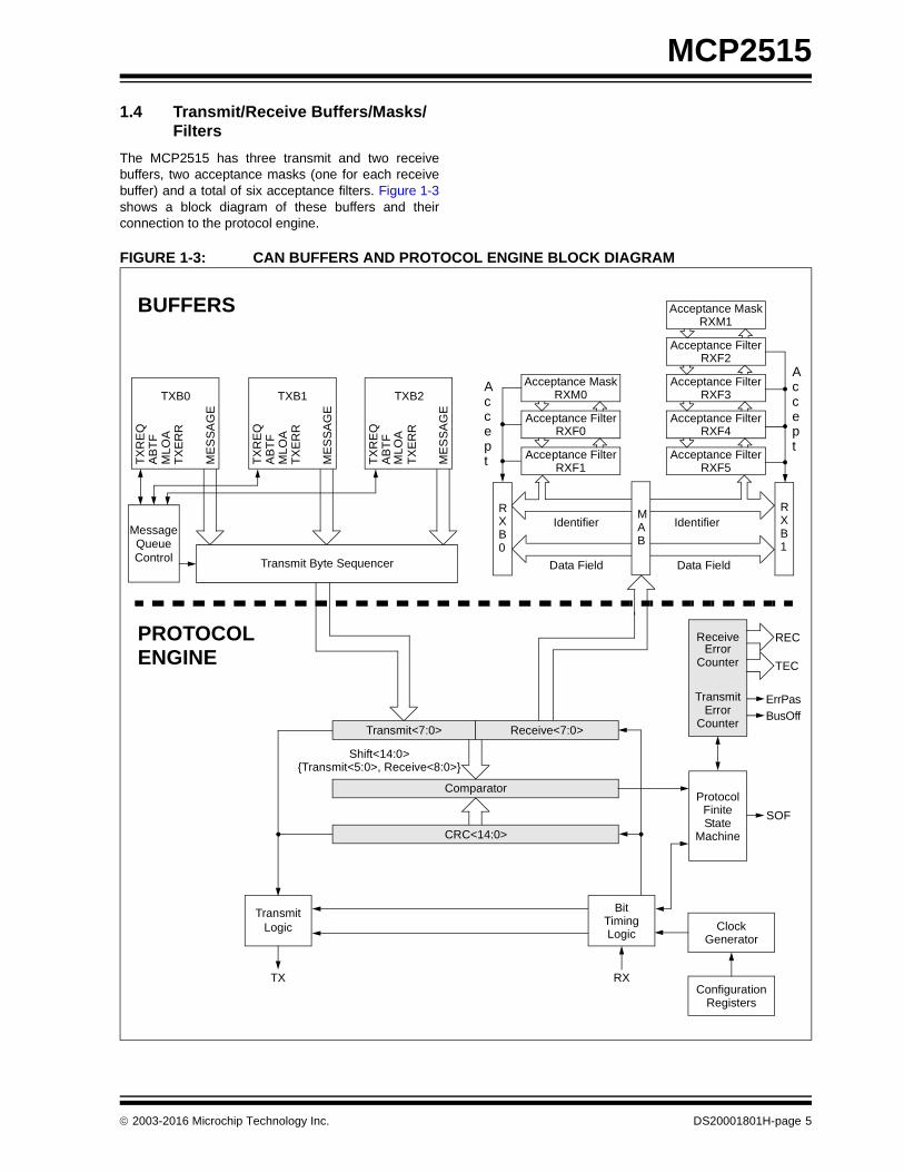
1.4 Transmit/Receive Buffers/Masks/Filters
The MCP2515 has three transmit and two receivebuffers, two acceptance masks (one for each receivebuffer) and a total of six acceptance filters. Figure 1-3shows a block diagram of these buffers and theirconnection to the protocol engine.
FIGURE 1-3: CAN BUFFERS AND PROTOCOL ENGINE BLOCK DIAGRAM
Acceptance FilterRXF2
RXB1
Identifier
Data Field Data Field
Identifier
Acceptance MaskRXM1
Acceptance FilterRXF3
Acceptance FilterRXF4
Acceptance FilterRXF5
MAB
Acceptance FilterRXF0
Acceptance FilterRXF1
RXB0
TX
RE
Q
TXB2A
BT
FM
LO
AT
XE
RR
ME
SS
AG
E
MessageQueueControl
TX
RE
Q
TXB0
AB
TF
ML
OA
TX
ER
R
ME
SS
AG
E
Comparator
ReceiveError
TransmitError
Protocol
REC
TEC
ErrPas
BusOff
FiniteState
Machine
Counter
Counter
Shift<14:0>{Transmit<5:0>, Receive<8:0>}
TransmitLogic
TX RXConfiguration
Registers
ClockGenerator
PROTOCOLENGINE
BUFFERS
TX
RE
Q
TXB1
AB
TF
ML
OA
TX
ER
R
ME
SS
AG
E
Acceptance MaskRXM0
Accept
Accept
SOF
BitTimingLogic
Receive<7:0>Transmit<7:0>
Transmit Byte Sequencer
CRC<14:0>
2003-2016 Microchip Technology Inc. DS20001801H-page 5
MCP2515
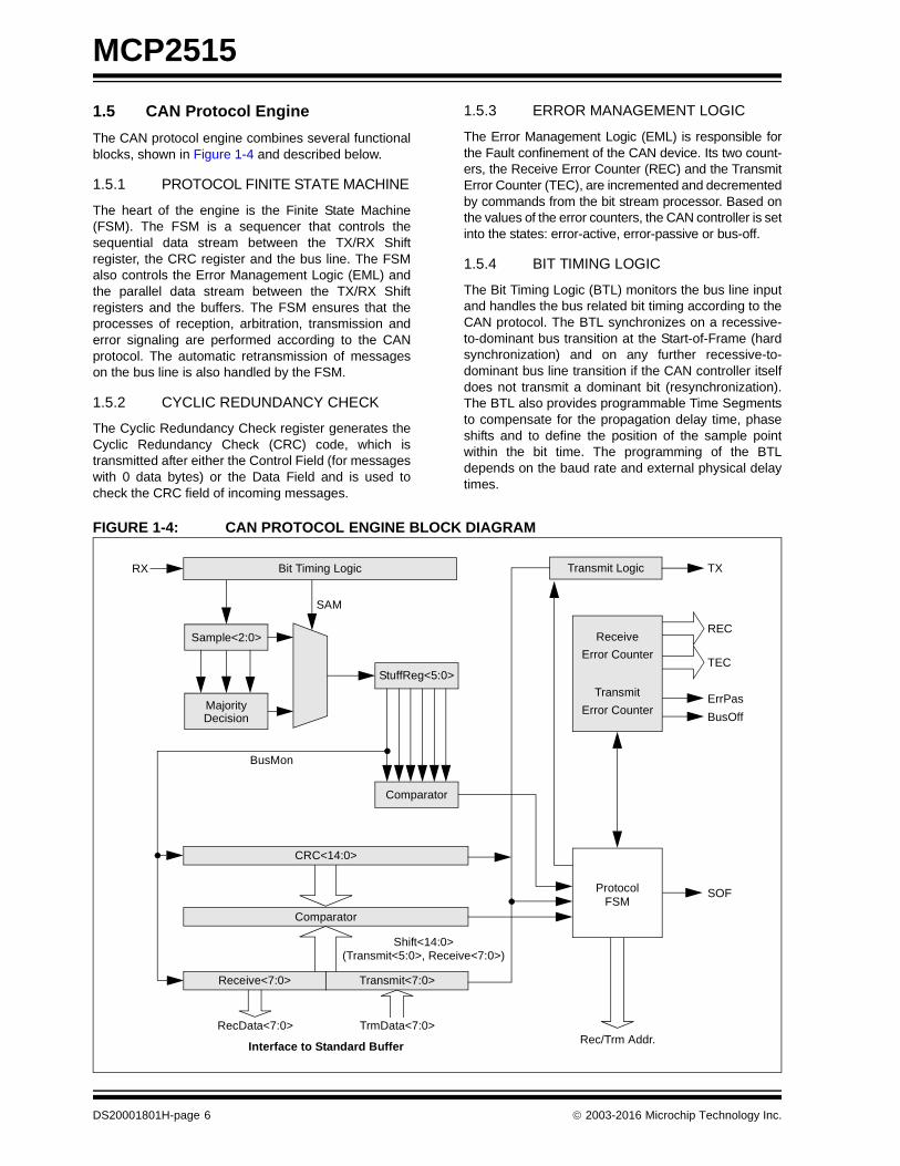
1.5 CAN Protocol Engine
The CAN protocol engine combines several functionalblocks, shown in Figure 1-4 and described below.
1.5.1 PROTOCOL FINITE STATE MACHINE
The heart of the engine is the Finite State Machine(FSM). The FSM is a sequencer that controls thesequential data stream between the TX/RX Shiftregister, the CRC register and the bus line. The FSMalso controls the Error Management Logic (EML) andthe parallel data stream between the TX/RX Shiftregisters and the buffers. The FSM ensures that theprocesses of reception, arbitration, transmission anderror signaling are performed according to the CANprotocol. The automatic retransmission of messageson the bus line is also handled by the FSM.
1.5.2 CYCLIC REDUNDANCY CHECK
The Cyclic Redundancy Check register generates theCyclic Redundancy Check (CRC) code, which istransmitted after either the Control Field (for messageswith 0 data bytes) or the Data Field and is used tocheck the CRC field of incoming messages.
1.5.3 ERROR MANAGEMENT LOGIC
The Error Management Logic (EML) is responsible forthe Fault confinement of the CAN device. Its two count-ers, the Receive Error Counter (REC) and the TransmitError Counter (TEC), are incremented and decrementedby commands from the bit stream processor. Based onthe values of the error counters, the CAN controller is setinto the states: error-active, error-passive or bus-off.
1.5.4 BIT TIMING LOGIC
The Bit Timing Logic (BTL) monitors the bus line inputand handles the bus related bit timing according to theCAN protocol. The BTL synchronizes on a recessive-to-dominant bus transition at the Start-of-Frame (hardsynchronization) and on any further recessive-to-dominant bus line transition if the CAN controller itselfdoes not transmit a dominant bit (resynchronization).The BTL also provides programmable Time Segmentsto compensate for the propagation delay time, phaseshifts and to define the position of the sample pointwithin the bit time. The programming of the BTLdepends on the baud rate and external physical delaytimes.
FIGURE 1-4: CAN PROTOCOL ENGINE BLOCK DIAGRAM
Bit Timing Logic
CRC<14:0>
Comparator
Receive<7:0> Transmit<7:0>
Sample<2:0>
MajorityDecision
StuffReg<5:0>
Comparator
Transmit Logic
Receive
Error Counter
Transmit
Error Counter
ProtocolFSM
RX
SAM
BusMon
Rec/Trm Addr.RecData<7:0> TrmData<7:0>
Shift<14:0>(Transmit<5:0>, Receive<7:0>)
TX
REC
TEC
ErrPas
BusOff
Interface to Standard Buffer
SOF
DS20001801H-page 6 2003-2016 Microchip Technology Inc.

MCP2515
2.0 CAN MESSAGE FRAMES
The MCP2515 supports standard data frames, extendeddata frames and remote frames (standard andextended), as defined in the CAN 2.0B specification.
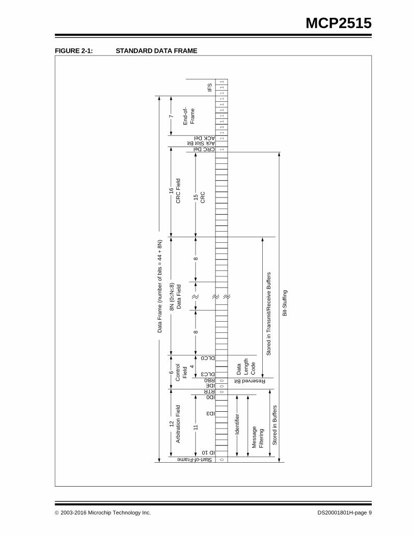
2.1 Standard Data Frame
The CAN standard data frame is shown in Figure 2-1.As with all other frames, the frame begins with a Start-of-Frame (SOF) bit, which is of the dominant state andallows hard synchronization of all nodes.
The SOF is followed by the arbitration field, consistingof 12 bits: the 11-bit identifier and the RemoteTransmission Request (RTR) bit. The RTR bit is usedto distinguish a data frame (RTR bit dominant) from aremote frame (RTR bit recessive).
Following the arbitration field is the control field,consisting of six bits. The first bit of this field is theIdentifier Extension (IDE) bit, which must be dominantto specify a standard frame. The following bit, ReservedBit Zero (RB0), is reserved and is defined as a dominantbit by the CAN protocol. The remaining four bits of thecontrol field are the Data Length Code (DLC), whichspecifies the number of bytes of data (0-8 bytes)contained in the message.
After the control field, is the data field, which containsany data bytes that are being sent, and is of the lengthdefined by the DLC (0-8 bytes).
The Cyclic Redundancy Check (CRC) field follows thedata field and is used to detect transmission errors. TheCRC field consists of a 15-bit CRC sequence, followedby the recessive CRC Delimiter bit.
The final field is the two-bit Acknowledge (ACK) field.During the ACK Slot bit, the transmitting node sendsout a recessive bit. Any node that has received anerror-free frame Acknowledges the correct reception ofthe frame by sending back a dominant bit (regardlessof whether the node is configured to accept thatspecific message or not). The recessive Acknowledgedelimiter completes the Acknowledge field and may notbe overwritten by a dominant bit.
2.2 Extended Data Frame
In the extended CAN data frame, shown in Figure 2-2,the SOF bit is followed by the arbitration field, whichconsists of 32 bits. The first 11 bits are the MostSignificant bits (MSb) (Base-lD) of the 29-bit identifier.These 11 bits are followed by the Substitute RemoteRequest (SRR) bit, which is defined to be recessive.The SRR bit is followed by the lDE bit, which isrecessive to denote an extended CAN frame.
It should be noted that if arbitration remains unresolvedafter transmission of the first 11 bits of the identifier, andone of the nodes involved in the arbitration is sending
a standard CAN frame (11-bit identifier), the standardCAN frame will win arbitration due to the assertion of adominant lDE bit. Also, the SRR bit in an extendedCAN frame must be recessive to allow the assertion ofa dominant RTR bit by a node that is sending astandard CAN remote frame.
The SRR and lDE bits are followed by the remaining18 bits of the identifier (Extended lD) and the RemoteTransmission Request bit.
To enable standard and extended frames to be sentacross a shared network, the 29-bit extended messageidentifier is split into 11-bit (Most Significant) and 18-bit(Least Significant) sections. This split ensures that thelDE bit can remain at the same bit position in both thestandard and extended frames.
Following the arbitration field is the six-bit control field.The first two bits of this field are reserved and must bedominant. The remaining four bits of the control fieldare the DLC, which specifies the number of data bytescontained in the message.
The remaining portion of the frame (data field, CRCfield, Acknowledge field, End-of-Frame and intermis-sion) is constructed in the same way as a standard dataframe (see Section 2.1 “Standard Data Frame”).
2.3 Remote Frame
Normally, data transmission is performed on anautonomous basis by the data source node (e.g., asensor sending out a data frame). It is possible,however, for a destination node to request data from thesource. To accomplish this, the destination node sendsa remote frame with an identifier that matches the iden-tifier of the required data frame. The appropriate datasource node will then send a data frame in response tothe remote frame request.
There are two differences between a remote frame(shown in Figure 2-3) and a data frame. First, the RTRbit is at the recessive state, and second, there is nodata field. In the event of a data frame and a remoteframe with the same identifier being transmitted at thesame time, the data frame wins arbitration due to thedominant RTR bit following the identifier. In this way,the node that transmitted the remote frame receivesthe desired data immediately.
2.4 Error Frame
An error frame is generated by any node that detects abus error. An error frame, shown in Figure 2-4, consistsof two fields: an error flag field followed by an errordelimiter field. There are two types of error flag fields.The type of error flag field sent depends upon the errorstatus of the node that detects and generates the errorflag field.
2003-2016 Microchip Technology Inc. DS20001801H-page 7

MCP2515
2.4.1 ACTIVE ERRORS
If an error-active node detects a bus error, the nodeinterrupts transmission of the current message bygenerating an active error flag. The active error flag iscomposed of six consecutive dominant bits. This bitsequence actively violates the bit-stuffing rule. All otherstations recognize the resulting bit-stuffing error, and inturn, generate error frames themselves, called errorecho flags.
The error flag field, therefore, consists of between sixand twelve consecutive dominant bits (generated byone or more nodes). The error delimiter field (eightrecessive bits) completes the error frame. Uponcompletion of the error frame, bus activity returns tonormal and the interrupted node attempts to resend theaborted message.
2.4.2 PASSIVE ERRORS
If an error-passive node detects a bus error, the nodetransmits an error-passive flag followed by the errordelimiter field. The error-passive flag consists of sixconsecutive recessive bits. The error frame for an error-passive node consists of 14 recessive bits. From this, itfollows that unless the bus error is detected by an error-active node or the transmitting node, the message willcontinue transmission because the error-passive flagdoes not interfere with the bus.
If the transmitting node generates an error-passive flag,it will cause other nodes to generate error frames due tothe resulting bit-stuffing violation. After transmission ofan error frame, an error-passive node must wait for sixconsecutive recessive bits on the bus before attemptingto rejoin bus communications.
The error delimiter consists of eight recessive bits, andallows the bus nodes to restart bus communicationscleanly after an error has occurred.
2.5 Overload Frame
An overload frame, shown in Figure 2-5, has the sameformat as an active-error frame. An overload frame,however, can only be generated during an interframespace. In this way, an overload frame can bedifferentiated from an error frame (an error frame issent during the transmission of a message). Theoverload frame consists of two fields: an overload flagfollowed by an overload delimiter. The overload flagconsists of six dominant bits followed by overload flagsgenerated by other nodes (and, as for an active errorflag, giving a maximum of twelve dominant bits). Theoverload delimiter consists of eight recessive bits. Anoverload frame can be generated by a node as a resultof two conditions:
1. The node detects a dominant bit during the inter-frame space, an illegal condition. Exception: Thedominant bit is detected during the third bit of IFS.In this case, the receivers will interpret this as aSOF.
2. Due to internal conditions, the node is not yetable to begin reception of the next message. Anode may generate a maximum of two sequentialoverload frames to delay the start of the nextmessage.
2.6 Interframe Space
The interframe space separates a preceding frame (ofany type) from a subsequent data or remote frame.The interframe space is composed of at least threerecessive bits, called the ‘Intermission’. This allowsnodes time for internal processing before the start ofthe next message frame. After the intermission, thebus line remains in the recessive state (Bus Idle) untilthe next transmission starts.
Note: Error echo flags typically occur when alocalized disturbance causes one or more(but not all) nodes to send an error flag.The remaining nodes generate error flagsin response (echo) to the original error flag.
Note: Case 2 should never occur with theMCP2515 due to very short internaldelays.
DS20001801H-page 8 2003-2016 Microchip Technology Inc.
MCP2515
FIGURE 2-1: STANDARD DATA FRAME
0000
11111111
Start-of-Frame
Da
ta F
ram
e (
nu
mb
er
of
bits
= 4
4 +
8N
)
12
Arb
itra
tion
Fie
ld
ID 10
11
ID3
ID0
Ide
ntif
ier
Me
ssa
ge
Filt
eri
ng
Sto
red
in B
uffe
rs
RTRIDERB0DLC3
DLC06
4
Co
ntr
ol
Fie
ld
Da
taL
en
gth
Co
de
Reserved Bit
8N
(0N
8)
Da
ta F
ield
88
Sto
red
in T
ran
smit/
Re
ceiv
e B
uffe
rs
Bit-
Stu
ffin
g
16
CR
C F
ield
15
CR
C
7
En
d-o
f-F
ram
e
CRC DelAck Slot BitACK Del
IFS
111
1
2003-2016 Microchip Technology Inc. DS20001801H-page 9

MCP2515
FIGURE 2-2: EXTENDED DATA FRAME
011
000
1
Start-of-Frame
Arb
itra
tion
Fie
ld
32
11
ID10
ID3
ID0
IDE
Ide
ntif
ier
Me
ssa
ge
Filt
eri
ng
Sto
red
in B
uffe
rs
SRR
EID17
EID0RTRRB1RB0DLC3
18
DLC0
6C
on
tro
lF
ield
4
Reserved BitsD
ata
Le
ng
thC
od
e
Sto
red
in T
ran
smit/
Re
ceiv
e B
uffe
rs
88
Da
ta F
ram
e (
nu
mb
er
of
bits
= 6
4 +
8N
)
8N
(0
N
8
)D
ata
Fie
ld
11111111
16
CR
C F
ield
15
CR
C
CRC DelAck Slot BitACK Del
En
d-o
f-F
ram
e
7
Bit-
Stu
ffin
g
IFS
Ext
ende
d Id
entif
ier
111
DS20001801H-page 10 2003-2016 Microchip Technology Inc.

MCP2515
FIGURE 2-3: REMOTE FRAME
011
100
Start-of-Frame
Arb
itra
tion
Fie
ld
32
11
ID10
ID3
ID0
IDE
Ide
ntif
ier
Me
ssa
ge
Filt
eri
ng
SRR
EID17
EID0RTRRB1RB0DLC3
18
DLC0
6C
on
tro
lF
ield
4
Reserved Bits
Da
taL
en
gth
Co
de
Ext
en
de
d I
de
ntif
ier
111111111
16
CR
C F
ield
15
CR
C
CRC DelAck Slot BitACK Del
En
d-o
f-F
ram
e
7
Re
mo
te F
ram
e w
ith E
xten
ded
Ide
ntifi
er
111
IFS
No
Dat
a F
ield
2003-2016 Microchip Technology Inc. DS20001801H-page 11

MCP2515
FIGURE 2-4: ACTIVE ERROR FRAME
0000
Start-of-Frame
Inte
rru
pte
d D
ata
Fra
me
12
Arb
itra
tion
Fie
ld
ID 10
11
ID3
ID0
Ide
ntif
ier
Me
ssa
ge
Filt
eri
ng
RTRIDERB0DLC3
DLC0
6
4
Co
ntr
ol
Fie
ld Da
ta
Le
ng
th
Co
de
Reserved Bit
8N
(0
N
8
)
Da
ta F
ield
88
Bit-
Stu
ffin
g
0000000
00111111110
Da
ta F
ram
e o
rR
em
ote
Fra
me
Err
or F
ram
e
6
Err
or
Fla
g
£ 6
Ech
oE
rro
rF
lag
8
Err
or
De
limite
r
Inte
r-F
ram
e S
pa
ce o
rO
verl
oa
d F
ram
e
DS20001801H-page 12 2003-2016 Microchip Technology Inc.

MCP2515
FIGURE 2-5: OVERLOAD FRAME
0100
111111111
Start-of-Frame
Re
mo
te F
ram
e (
nu
mb
er
of
bits
= 4
4)
12
Arb
itra
tion
Fie
ld
ID 10
11
ID0RTRIDERB0DLC3
DLC0
6
4
Co
ntr
ol
Fie
ld
16
CR
C F
ield
15
CR
C
7
En
d-o
f-F
ram
e
CRC DelAck Slot BitACK Del
000000011111111
Ove
rlo
ad
Fra
me
En
d-o
f-F
ram
e o
rE
rro
r D
elim
iter
or
Ove
rlo
ad
De
limite
r
6
Ove
rlo
ad
Fla
g
Ove
rlo
ad
De
limite
r
8In
ter-
Fra
me
Spa
ce o
rE
rror
Fra
me
2003-2016 Microchip Technology Inc. DS20001801H-page 13

MCP2515
NOTES:
DS20001801H-page 14 2003-2016 Microchip Technology Inc.

MCP2515
3.0 MESSAGE TRANSMISSION
3.1 Transmit Buffers
The MCP2515 implements three transmit buffers. Eachof these buffers occupies 14 bytes of SRAM and aremapped into the device memory map.
The first byte, TXBnCTRL, is a control registerassociated with the message buffer. The information inthis register determines the conditions under which themessage will be transmitted and indicates the status ofthe message transmission (see Register 3-1).
Five bytes are used to hold the Standard and ExtendedIdentifiers, as well as other message arbitration infor-mation (see Register 3-3 through Register 3-6). Thelast eight bytes are for the eight possible data bytes ofthe message to be transmitted (see Register 3-8).
At a minimum, the TXBnSIDH, TXBnSIDL and TXBnDLCregisters must be loaded. If data bytes are present in themessage, the TXBnDm registers must also be loaded.If the message is to use Extended Identifiers, theTXBnEIDm registers must also be loaded and theEXIDE (TXBnSIDL<3>) bit set.
Prior to sending the message, the MCU must initializethe TXnIE bit in the CANINTE register to enable ordisable the generation of an interrupt when the messageis sent.
3.2 Transmit Priority
Transmit priority is a prioritization within the MCP2515of the pending transmittable messages. This isindependent from, and not necessarily related to, anyprioritization implicit in the message arbitration schemebuilt into the CAN protocol.
Prior to sending the SOF, the priority of all buffers thatare queued for transmission is compared. The transmitbuffer with the highest priority will be sent first. Forexample, if Transmit Buffer 0 has a higher prioritysetting than Transmit Buffer 1, Transmit Buffer 0 will besent first.
If two buffers have the same priority setting, the bufferwith the highest buffer number will be sent first. Forexample, if Transmit Buffer 1 has the same prioritysetting as Transmit Buffer 0, Transmit Buffer 1 will besent first.
There are four levels of transmit priority. If theTXP<1:0> bits (TXBnCTRL<1:0>) for a particular mes-sage buffer are set to ‘11’, that buffer has the highestpossible priority. If the TXP<1:0> bits for a particularmessage buffer are ‘00’, that buffer has the lowestpossible priority.
3.3 Initiating Transmission
In order to initiate message transmission, the TXREQbit (TXBnCTRL<3>) must be set for each buffer to betransmitted. This can be accomplished by:
• Writing to the register via the SPI write command
• Sending the SPI RTS command
• Setting the TXnRTS pin low for the particular transmit buffer(s) that are to be transmitted
If transmission is initiated via the SPI interface, theTXREQ bit can be set at the same time as the TXPxpriority bits.
When TXREQ is set, the ABTF, MLOA and TXERR bits(TXBnCTRL<5:4>) will be cleared automatically.
Once the transmission has completed successfully, theTXREQ bit will be cleared, the TXnIF bit (CANINTF) willbe set and an interrupt will be generated if the TXnIE bit(CANINTE) is set.
If the message transmission fails, the TXREQ bit willremain set. This indicates that the message is stillpending for transmission and one of the followingcondition flags will be set:
• If the message started to transmit but encountered an error condition, the TXERR (TXBnCTRL<4>) and MERRF bits (CANINTF<7>) will be set, and an interrupt will be generated on the INT pin if the MERRE bit (CANINTE<7>) is set
• If the message is lost, arbitration at the MLOA bit (TXBnCTRL<5>) will be set
3.4 One-Shot Mode
One-Shot mode ensures that a message will onlyattempt to transmit one time. Normally, if a CANmessage loses arbitration, or is destroyed by an errorframe, the message is retransmitted. With One-Shotmode enabled, a message will only attempt to transmitone time, regardless of arbitration loss or error frame.
One-Shot mode is required to maintain time slots indeterministic systems, such as TTCAN.
Note: The TXREQ bit (TXBnCTRL<3>) must beclear (indicating the transmit buffer is notpending transmission) before writing tothe transmit buffer.
Note: Setting the TXREQ bit (TXBnCTRL<3>)does not initiate a message transmission.It merely flags a message buffer as beingready for transmission. Transmission willstart when the device detects that the busis available.
Note: If One-Shot mode is enabled (OSM bit(CANCTRL<3>)), the above conditions willstill exist. However, the TXREQ bit will becleared and the message will not attempttransmission a second time.
2003-2016 Microchip Technology Inc. DS20001801H-page 15
MCP2515
3.5 TXnRTS Pins
The TXnRTS pins are input pins that can be configuredas:
• Request-to-Send inputs, which provide an alternative means of initiating the transmission of a message from any of the transmit buffers
• Standard digital inputs
Configuration and control of these pins is accomplishedusing the TXRTSCTRL register (see Register 3-2). TheTXRTSCTRL register can only be modified when theMCP2515 is in Configuration mode (see Section 10.0“Modes of Operation”). If configured to operate as aRequest-to-Send pin, the pin is mapped into therespective TXREQ bit (TXBnCTRL<3>) for the transmitbuffer. The TXREQ bit is latched by the falling edge ofthe TXnRTS pin. The TXnRTS pins are designed toallow them to be tied directly to the RXnBF pins toautomatically initiate a message transmission when theRXnBF pin goes low.
The TXnRTS pins have internal pull-up resistors of100 k (nominal).
3.6 Aborting Transmission
The MCU can request to abort a message in a specificmessage buffer by clearing the associated TXREQ bit.
In addition, all pending messages can be requested tobe aborted by setting the ABAT bit (CANCTRL<4>).This bit MUST be reset (typically after the TXREQ bitshave been verified to be cleared) to continue transmit-ting messages. The ABTF flag (TXBnCTRL<6>) willonly be set if the abort was requested via the ABAT bit.Aborting a message by resetting the TXREQ bit doesNOT cause the ABTF bit to be set.
Note 1: Messages that were transmitting whenthe abort was requested will continue totransmit. If the message does not suc-cessfully complete transmission (i.e., lostarbitration or was interrupted by an errorframe), it will then be aborted.
2: When One-Shot mode is enabled, if themessage is interrupted due to an errorframe or loss of arbitration, the ABTF bitwill set.
DS20001801H-page 16 2003-2016 Microchip Technology Inc.
MCP2515
FIGURE 3-1: TRANSMIT MESSAGE FLOWCHART
Start
IsCAN bus available
to start transmission?
No
Examine TXP<1:0> (TXBnCTRL<1:0>)
Are anyTXREQ (TXBnCTRL<3>)
bits = 1?
The message transmission sequence begins when the device determines that the TXREQ bit (TXBnCTRL<3>) for any of the transmit registers has been set.
Clear: ABTF (TXBnCTRL<6>)MLOA (TXBnCTRL<5>)TXERR (TXBnCTRL<4>)
Yes
IsTXREQ = 0
or ABAT = 1?
Clearing the TXREQ bit while it is set, or setting the ABAT bit (CANCTRL<4>) before the message has started transmission, will abort the message.
No
Transmit Message
WasMessage Transmitted
Successfully?
No
Yes
Clear TXREQ bit
TXnIE (CANINTE) = 1?GenerateInterrupt
Yes
Message
Yes
Set
SetTXERR (TXBnCTRL<4>)
Lost
to Determine Highest Priority Message
No
SetMLOA (TXBnCTRL<5>)
The TXnIE bit determines if an interrupt should be generated when a message is successfully transmitted.
GOTO START
TXnIF (CANTINF)
Yes
No
Message erroror
lost arbitration
Arbitration
Error
MERRE (CANINTE)?
NoGenerateInterrupt
Yes
SetMERRF (CANTINF)
?
2003-2016 Microchip Technology Inc. DS20001801H-page 17
MCP2515
REGISTER 3-1: TXBnCTRL: TRANSMIT BUFFER n CONTROL REGISTER(ADDRESS: 30h, 40h, 50h)
U-0 R-0 R-0 R-0 R/W-0 U-0 R/W-0 R/W-0
— ABTF MLOA TXERR TXREQ — TXP1 TXP0
bit 7 bit 0
Legend:
R = Readable bit W = Writable bit U = Unimplemented bit, read as ‘0’
-n = Value at POR ‘1’ = Bit is set ‘0’ = Bit is cleared x = Bit is unknown
bit 7 Unimplemented: Read as ‘0’
bit 6 ABTF: Message Aborted Flag bit
1 = Message was aborted0 = Message completed transmission successfully
bit 5 MLOA: Message Lost Arbitration bit
1 = Message lost arbitration while being sent0 = Message did not lose arbitration while being sent
bit 4 TXERR: Transmission Error Detected bit
1 = A bus error occurred while the message was being transmitted0 = No bus error occurred while the message was being transmitted
bit 3 TXREQ: Message Transmit Request bit
1 = Buffer is currently pending transmission(MCU sets this bit to request message be transmitted – bit is automatically cleared when themessage is sent)
0 = Buffer is not currently pending transmission(MCU can clear this bit to request a message abort)
bit 2 Unimplemented: Read as ‘0’
bit 1-0 TXP<1:0>: Transmit Buffer Priority bits
11 = Highest message priority10 = High intermediate message priority01 = Low intermediate message priority00 = Lowest message priority
DS20001801H-page 18 2003-2016 Microchip Technology Inc.

MCP2515
REGISTER 3-2: TXRTSCTRL: TXnRTS PIN CONTROL AND STATUS REGISTER(ADDRESS: 0Dh)
U-0 U-0 R-x R-x R-x R/W-0 R/W-0 R/W-0
— — B2RTS B1RTS B0RTS B2RTSM B1RTSM B0RTSM
bit 7 bit 0
Legend:
R = Readable bit W = Writable bit U = Unimplemented bit, read as ‘0’
-n = Value at POR ‘1’ = Bit is set ‘0’ = Bit is cleared x = Bit is unknown
bit 7-6 Unimplemented: Read as ‘0’
bit 5 B2RTS: TX2RTS Pin State bit
- Reads state of TX2RTS pin when in Digital Input mode- Reads as ‘0’ when pin is in Request-to-Send mode
bit 4 B1RTS: TX1RTS Pin State bit
- Reads state of TX1RTS pin when in Digital Input mode- Reads as ‘0’ when pin is in Request-to-Send mode
bit 3 B0RTS: TX0RTS Pin State bit
- Reads state of TX0RTS pin when in Digital Input mode- Reads as ‘0’ when pin is in Request-to-Send mode
bit 2 B2RTSM: TX2RTS Pin mode bit
1 = Pin is used to request message transmission of TXB2 buffer (on falling edge)0 = Digital input
bit 1 B1RTSM: TX1RTS Pin mode bit
1 = Pin is used to request message transmission of TXB1 buffer (on falling edge)0 = Digital input
bit 0 B0RTSM: TX0RTS Pin mode bit
1 = Pin is used to request message transmission of TXB0 buffer (on falling edge)0 = Digital input
2003-2016 Microchip Technology Inc. DS20001801H-page 19

MCP2515
REGISTER 3-3: TXBnSIDH: TRANSMIT BUFFER n STANDARD IDENTIFIER REGISTER HIGH(ADDRESS: 31h, 41h, 51h)
R/W-x R/W-x R/W-x R/W-x R/W-x R/W-x R/W-x R/W-x
SID10 SID9 SID8 SID7 SID6 SID5 SID4 SID3
bit 7 bit 0
Legend:
R = Readable bit W = Writable bit U = Unimplemented bit, read as ‘0’
-n = Value at POR ‘1’ = Bit is set ‘0’ = Bit is cleared x = Bit is unknown
bit 7-0 SID<10:3>: Standard Identifier bits
REGISTER 3-4: TXBnSIDL: TRANSMIT BUFFER n STANDARD IDENTIFIER REGISTER LOW(ADDRESS: 32h, 42h, 52h)
R/W-x R/W-x R/W-x U-0 R/W-x U-0 R/W-x R/W-x
SID2 SID1 SID0 — EXIDE — EID17 EID16
bit 7 bit 0
Legend:
R = Readable bit W = Writable bit U = Unimplemented bit, read as ‘0’
-n = Value at POR ‘1’ = Bit is set ‘0’ = Bit is cleared x = Bit is unknown
bit 7-5 SID<2:0>: Standard Identifier bits
bit 4 Unimplemented: Read as ‘0’
bit 3 EXIDE: Extended Identifier Enable bit
1 = Message will transmit Extended Identifier0 = Message will transmit Standard Identifier
bit 2 Unimplemented: Read as ‘0’
bit 1-0 EID<17:16>: Extended Identifier bits
DS20001801H-page 20 2003-2016 Microchip Technology Inc.
MCP2515
REGISTER 3-5: TXBnEID8: TRANSMIT BUFFER n EXTENDED IDENTIFIER 8 REGISTER HIGH(ADDRESS: 33h, 43h, 53h)
R/W-x R/W-x R/W-x R/W-x R/W-x R/W-x R/W-x R/W-x
EID15 EID14 EID13 EID12 EID11 EID10 EID9 EID8
bit 7 bit 0
Legend:
R = Readable bit W = Writable bit U = Unimplemented bit, read as ‘0’
-n = Value at POR ‘1’ = Bit is set ‘0’ = Bit is cleared x = Bit is unknown
bit 7-0 EID<15:8>: Extended Identifier bits
REGISTER 3-6: TXBnEID0: TRANSMIT BUFFER n EXTENDED IDENTIFIER 0 REGISTER LOW(ADDRESS: 34h, 44h, 54h)
R/W-x R/W-x R/W-x R/W-x R/W-x R/W-x R/W-x R/W-x
EID7 EID6 EID5 EID4 EID3 EID2 EID1 EID0
bit 7 bit 0
Legend:
R = Readable bit W = Writable bit U = Unimplemented bit, read as ‘0’
-n = Value at POR ‘1’ = Bit is set ‘0’ = Bit is cleared x = Bit is unknown
bit 7-0 EID<7:0>: Extended Identifier bits
2003-2016 Microchip Technology Inc. DS20001801H-page 21

MCP2515
REGISTER 3-7: TXBnDLC: TRANSMIT BUFFER n DATA LENGTH CODE REGISTER(ADDRESS: 35h, 45h, 55h)
U-0 R/W-x U-0 U-0 R/W-x R/W-x R/W-x R/W-x
— RTR — — DLC3(1) DLC2(1) DLC1(1) DLC0(1)
bit 7 bit 0
Legend:
R = Readable bit W = Writable bit U = Unimplemented bit, read as ‘0’
-n = Value at POR ‘1’ = Bit is set ‘0’ = Bit is cleared x = Bit is unknown
bit 7 Unimplemented: Read as ‘0’
bit 6 RTR: Remote Transmission Request bit
1 = Transmitted message will be a remote transmit request0 = Transmitted message will be a data frame
bit 5-4 Unimplemented: Reads as ‘0’
bit 3-0 DLC<3:0>: Data Length Code bits(1)
Sets the number of data bytes to be transmitted (0 to 8 bytes).
Note 1: It is possible to set the DLC<3:0> bits to a value greater than eight; however, only eight bytes are transmitted.
REGISTER 3-8: TXBnDm: TRANSMIT BUFFER n DATA BYTE m REGISTER(ADDRESS: 36h-3Dh, 46h-4Dh, 56h-5Dh)
R/W-x R/W-x R/W-x R/W-x R/W-x R/W-x R/W-x R/W-x
TXBnDm7 TXBnDm6 TXBnDm5 TXBnDm4 TXBnDm3 TXBnDm2 TXBnDm1 TXBnDm0
bit 7 bit 0
Legend:
R = Readable bit W = Writable bit U = Unimplemented bit, read as ‘0’
-n = Value at POR ‘1’ = Bit is set ‘0’ = Bit is cleared x = Bit is unknown
bit 7-0 TXBnDm<7:0>: Transmit Buffer n Data Field Byte m bits
DS20001801H-page 22 2003-2016 Microchip Technology Inc.

MCP2515
4.0 MESSAGE RECEPTION
4.1 Receive Message Buffering
The MCP2515 includes two full receive buffers withmultiple acceptance filters for each. There is also aseparate Message Assembly Buffer (MAB) that acts asa third receive buffer (see Figure 4-2).
4.1.1 MESSAGE ASSEMBLY BUFFER
Of the three receive buffers, the MAB is alwayscommitted to receiving the next message from the bus.The MAB assembles all messages received. Thesemessages will be transferred to the RXBn buffers (seeRegister 4-4 to Register 4-9) only if the acceptancefilter criteria is met.
4.1.2 RXB0 AND RXB1
The remaining two receive buffers, called RXB0 andRXB1, can receive a complete message from theprotocol engine via the MAB. The MCU can access onebuffer, while the other buffer is available for messagereception, or for holding a previously receivedmessage.
4.1.3 RECEIVE FLAGS/INTERRUPTS
When a message is moved into either of the receivebuffers, the appropriate RXnIF bit (CANINTF) is set.This bit must be cleared by the MCU in order to allow anew message to be received into the buffer. This bitprovides a positive lockout to ensure that the MCU hasfinished with the message before the MCP2515attempts to load a new message into the receive buffer.
If the RXnIE bit (CANINTE) is set, an interrupt will begenerated on the INT pin to indicate that a validmessage has been received. In addition, the associ-ated RXnBF pin will drive low if configured as a receivebuffer full pin. See Section 4.4 “RX0BF and RX1BFPins” for details.
4.2 Receive Priority
RXB0, the higher priority buffer, has one mask and twomessage acceptance filters associated with it. Thereceived message is applied to the mask and filters forRXB0 first.
RXB1 is the lower priority buffer, with one mask andfour acceptance filters associated with it.
In addition to the message being applied to the RXB0mask and filters first, the lower number of acceptancefilters makes the match on RXB0 more restrictive andimplies a higher priority for that buffer.
When a message is received, the RXBnCTRL<3:0>register bits will indicate the acceptance filter numberthat enabled reception and whether the receivedmessage is a Remote Transfer Request.
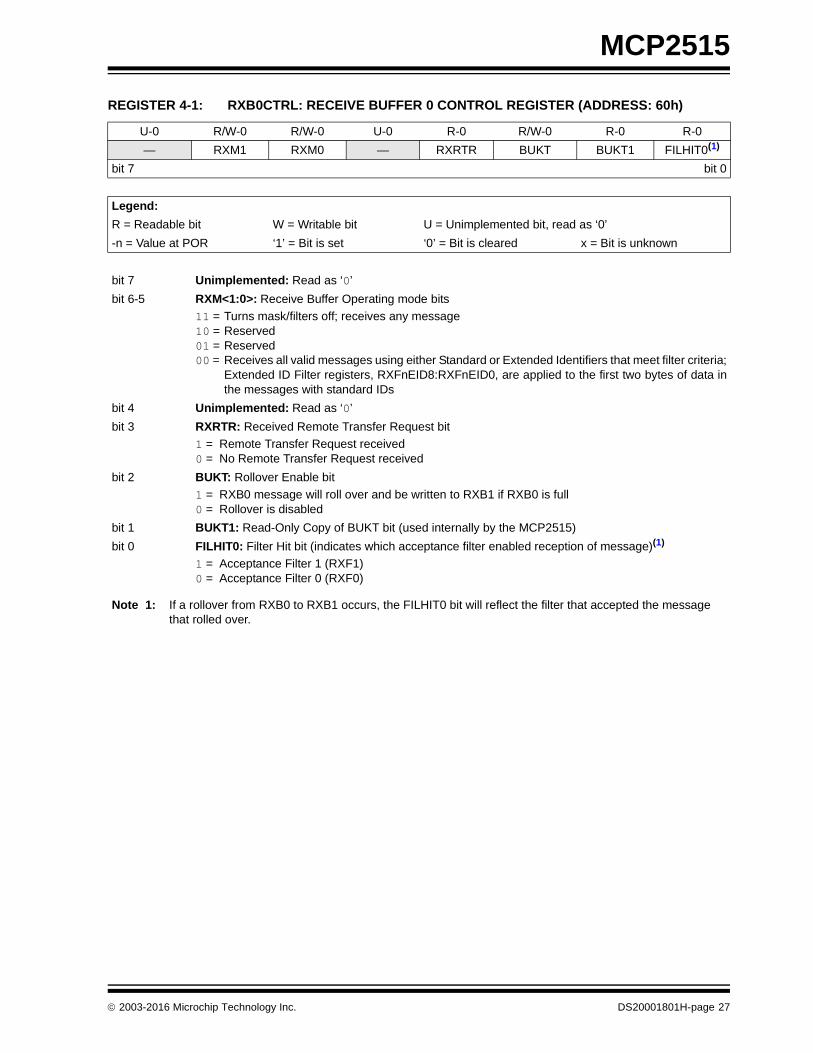
4.2.1 ROLLOVER
Additionally, the RXB0CTRL register can be configuredsuch that, if RXB0 contains a valid message andanother valid message is received, an overflow errorwill not occur and the new message will be moved intoRXB1, regardless of the acceptance criteria of RXB1.
4.2.2 RXM BITS
The RXM<1:0> bits (RXBnCTRL<6:5>) set specialReceive modes. Normally, these bits are cleared to ‘00’to enable reception of all valid messages as deter-mined by the appropriate acceptance filters. In thiscase, the determination of whether or not to receivestandard or extended messages is determined by theEXIDE bit (RFXnSIDL<3>) in the Filter n StandardIdentifier Low register.
If the RXM<1:0> bits are set to ‘11’, the buffer willreceive all messages, regardless of the values of theacceptance filters. Also, if a message has an errorbefore the EOF, that portion of the message assembledin the MAB, before the error frame, will be loaded intothe buffer. This mode has some value in debugging aCAN system and would not be used in an actualsystem environment.
Setting the RXM<1:0> bits to ‘01’ or ‘10’ is notrecommended.
Note: The entire content of the MAB is movedinto the receive buffer once a message isaccepted. This means, that regardless ofthe type of identifier (Standard orExtended) and the number of data bytesreceived, the entire receive buffer isoverwritten with the MAB contents.Therefore, the contents of all registers inthe buffer must be assumed to have beenmodified when any message is received.
2003-2016 Microchip Technology Inc. DS20001801H-page 23

MCP2515
4.3 Start-of-Frame Signal
If enabled, the Start-of-Frame signal is generated onthe SOF pin at the beginning of each CAN messagedetected on the RXCAN pin.
The RXCAN pin monitors an Idle bus for a recessive-to-dominant edge. If the dominant condition remainsuntil the sample point, the MCP2515 interprets this asa SOF and a SOF pulse is generated. If the dominantcondition does not remain until the sample point, theMCP2515 interprets this as a glitch on the bus and noSOF signal is generated. Figure 4-1 illustrates SOFsignaling and glitch filtering.
As with One-Shot mode, one use for SOF signaling isfor TTCAN-type systems. In addition, by monitoringboth the RXCAN pin and the SOF pin, an MCU candetect early physical bus problems by detecting smallglitches before they affect the CAN communications.
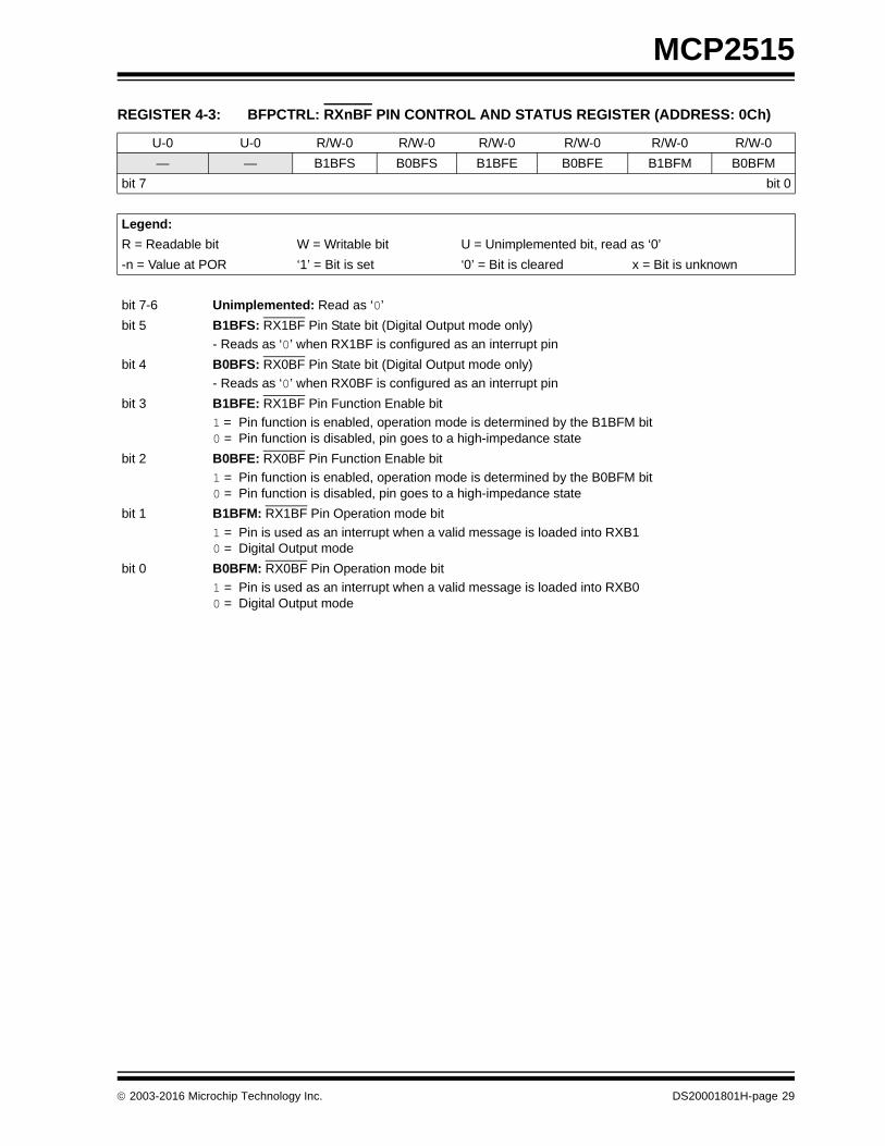
4.4 RX0BF and RX1BF Pins
In addition to the INT pin, which provides an interruptsignal to the MCU for many different conditions, theReceive Buffer Full pins (RX0BF and RX1BF) can beused to indicate that a valid message has been loadedinto RXB0 or RXB1, respectively. The pins have threedifferent configurations (Table 4-1):
1. Disabled2. Buffer Full Interrupt3. Digital Output
4.4.1 DISABLED
The RXnBF pins can be disabled to the high-impedancestate by clearing the BnBFE bits (BFPCTRL<3:2>).
4.4.2 CONFIGURED AS BUFFER FULL
The RXnBF pins can be configured to act as either buf-fer full interrupt pins or as standard digital outputs.Configuration and status of these pins are available viathe BFPCTRL register (Register 4-3). When set tooperate in Interrupt mode, by setting the BnBFE andBnBFM bits (BFPCTRL<3:0>), these pins are active-low and are mapped to the RXnIF bit (CANINTF) foreach receive buffer. When this bit goes high for one ofthe receive buffers (indicating that a valid message hasbeen loaded into the buffer), the corresponding RXnBFpin will go low. When the RXnIF bit is cleared by theMCU, the corresponding interrupt pin will go to the logichigh state until the next message is loaded into thereceive buffer.
FIGURE 4-1: START-OF-FRAME SIGNALING
START-OF-FRAME BIT
SamplePoint
ID Bit
RXCAN
SOF
EXPECTED START-OF-FRAME BIT
SamplePoint Bus Idle
RXCAN
SOF
Expected
Normal SOF Signaling
Glitch Filtering
DS20001801H-page 24 2003-2016 Microchip Technology Inc.
MCP2515
4.4.3 CONFIGURED AS DIGITAL OUTPUT
When used as digital outputs, the BnBFM bits(BFPCTRL<1:0>) must be cleared and the BnBFE bits(BFPCTRL<3:2>) must be set for the associated buffer.In this mode, the state of the pin is controlled by theBnBFS bits (BFPCTRL<5:4>). Writing a ‘1’ to a BnBFSbit will cause a high level to be driven on the associatedbuffer full pin, while a ‘0’ will cause the pin to drive low.When using the pins in this mode, the state of the pinshould be modified only by using the SPI BIT MODIFYcommand to prevent glitches from occurring on eitherof the buffer full pins.
TABLE 4-1: CONFIGURING RXnBF PINS
FIGURE 4-2: RECEIVE BUFFER BLOCK DIAGRAM
BnBFE BnBFM BnBFS Pin Status
0 X X Disabled, high-impedance
1 1 X Receive buffer interrupt
1 0 0 Digital output = 0
1 0 1 Digital output = 1
Acceptance MaskRXM1
Acceptance FilterRXF2
Acceptance FilterRXF3
Acceptance FilterRXF4
Acceptance FilterRXF5
Acceptance MaskRXM0
Acceptance FilterRXF0
Acceptance FilterRXF1
Identifier
Data Field Data Field
Identifier
Note: Messages received in the MAB are initiallyapplied to the mask and filters of RXB0. Inaddition, only one filter match occurs (e.g.,if the message matches both RXF0 andRXF2, the match will be for RXF0 and themessage will be moved into RXB0).
Accept
Accept
RXB0
RXB1
MAB
2003-2016 Microchip Technology Inc. DS20001801H-page 25
MCP2515
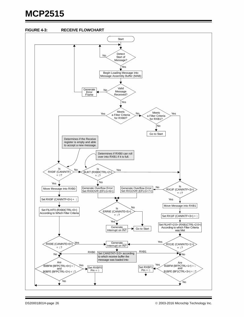
FIGURE 4-3: RECEIVE FLOWCHART
Set RXBF0
Start
DetectStart of
Message?
ValidMessage
Received?
GenerateError
Meetsa Filter Criteria
IsRX0IF (CANINTF)
Go to Start
Move Message into RXB0
Set FILHIT<2:0> (RXB1CTRL<2:0>)
IsRX1IF (CANINTF<3>)
Move Message into RXB1
Set RX1IF (CANINTF<3>) = 1
Yes
No
GenerateInterrupt on INT
Yes Yes
No No
Yes
Yes
No
No
Yes
Yes
Frame
No Yes
No
Begin Loading Message intoMessage Assembly Buffer (MAB)
According to which Filter Criteriawas Met
Set FILHIT0 (RXB0CTRL<0>)According to Which Filter Criteria
Set CANSTAT<3:0> according to which receive buffer the message was loaded into
IsBUKT (RXB0CTRL<2>)
Generate Overflow Error:Set RX1OVR (EFLG<7>)
IsERRIE (CANINTE<5>)
No
Go to Start
Yes
No
AreB0BFM (BFPCTRL<0>) = 1
B0BFE (BFPCTRL<2>) = 1?and
Pin = 0
No
Set RXBF1Pin = 0
No
YesYes
RX0IE (CANINTE<0>) RX1IE (CANINTE<1>)
RXB1RXB0
Set RX0OVR (EFLG<6>)Generate Overflow Error:
Set RX0IF (CANINTF<0>) = 1
AreB1BFM (BFPCTRL<1>) = 1
B1BFE (BF1CTRL<3>) = 1?and
Meetsa Filter Criteria
for RXB1?for RXB0?
No Yes
GenerateInterrupt on INT
Determines if the Receiveregister is empty and ableto accept a new message.
Determines if RXB0 can rollover into RXB1 if it is full.
= 0?
= 1?
= 1?
= 1?
= 0?
= 1?
DS20001801H-page 26 2003-2016 Microchip Technology Inc.
MCP2515
REGISTER 4-1: RXB0CTRL: RECEIVE BUFFER 0 CONTROL REGISTER (ADDRESS: 60h)
U-0 R/W-0 R/W-0 U-0 R-0 R/W-0 R-0 R-0
— RXM1 RXM0 — RXRTR BUKT BUKT1 FILHIT0(1)
bit 7 bit 0
Legend:
R = Readable bit W = Writable bit U = Unimplemented bit, read as ‘0’
-n = Value at POR ‘1’ = Bit is set ‘0’ = Bit is cleared x = Bit is unknown
bit 7 Unimplemented: Read as ‘0’
bit 6-5 RXM<1:0>: Receive Buffer Operating mode bits
11 = Turns mask/filters off; receives any message10 = Reserved01 = Reserved00 = Receives all valid messages using either Standard or Extended Identifiers that meet filter criteria;
Extended ID Filter registers, RXFnEID8:RXFnEID0, are applied to the first two bytes of data inthe messages with standard IDs
bit 4 Unimplemented: Read as ‘0’
bit 3 RXRTR: Received Remote Transfer Request bit
1 = Remote Transfer Request received0 = No Remote Transfer Request received
bit 2 BUKT: Rollover Enable bit
1 = RXB0 message will roll over and be written to RXB1 if RXB0 is full0 = Rollover is disabled
bit 1 BUKT1: Read-Only Copy of BUKT bit (used internally by the MCP2515)
bit 0 FILHIT0: Filter Hit bit (indicates which acceptance filter enabled reception of message)(1)
1 = Acceptance Filter 1 (RXF1)0 = Acceptance Filter 0 (RXF0)
Note 1: If a rollover from RXB0 to RXB1 occurs, the FILHIT0 bit will reflect the filter that accepted the message that rolled over.
2003-2016 Microchip Technology Inc. DS20001801H-page 27

MCP2515
REGISTER 4-2: RXB1CTRL: RECEIVE BUFFER 1 CONTROL REGISTER (ADDRESS: 70h)
U-0 R/W-0 R/W-0 U-0 R-0 R-0 R-0 R-0
— RXM1 RXM0 — RXRTR FILHIT2 FILHIT1 FILHIT0
bit 7 bit 0
Legend:
R = Readable bit W = Writable bit U = Unimplemented bit, read as ‘0’
-n = Value at POR ‘1’ = Bit is set ‘0’ = Bit is cleared x = Bit is unknown
bit 7 Unimplemented: Read as ‘0’
bit 6-5 RXM<1:0>: Receive Buffer Operating mode bits
11 = Turns mask/filters off; receives any message10 = Reserved01 = Reserved00 = Receives all valid messages using either Standard or Extended Identifiers that meet filter criteria
bit 4 Unimplemented: Read as ‘0’
bit 3 RXRTR: Received Remote Transfer Request bit
1 = Remote Transfer Request received0 = No Remote Transfer Request received
bit 2-0 FILHIT<2:0>: Filter Hit bits (indicates which acceptance filter enabled reception of message)
101 = Acceptance Filter 5 (RXF5)100 = Acceptance Filter 4 (RXF4)011 = Acceptance Filter 3 (RXF3)010 = Acceptance Filter 2 (RXF2)001 = Acceptance Filter 1 (RXF1) (only if the BUKT bit is set in RXB0CTRL)000 = Acceptance Filter 0 (RXF0) (only if the BUKT bit is set in RXB0CTRL)
DS20001801H-page 28 2003-2016 Microchip Technology Inc.
MCP2515
REGISTER 4-3: BFPCTRL: RXnBF PIN CONTROL AND STATUS REGISTER (ADDRESS: 0Ch)
U-0 U-0 R/W-0 R/W-0 R/W-0 R/W-0 R/W-0 R/W-0
— — B1BFS B0BFS B1BFE B0BFE B1BFM B0BFM
bit 7 bit 0
Legend:
R = Readable bit W = Writable bit U = Unimplemented bit, read as ‘0’
-n = Value at POR ‘1’ = Bit is set ‘0’ = Bit is cleared x = Bit is unknown
bit 7-6 Unimplemented: Read as ‘0’
bit 5 B1BFS: RX1BF Pin State bit (Digital Output mode only)
- Reads as ‘0’ when RX1BF is configured as an interrupt pin
bit 4 B0BFS: RX0BF Pin State bit (Digital Output mode only)
- Reads as ‘0’ when RX0BF is configured as an interrupt pin
bit 3 B1BFE: RX1BF Pin Function Enable bit
1 = Pin function is enabled, operation mode is determined by the B1BFM bit0 = Pin function is disabled, pin goes to a high-impedance state
bit 2 B0BFE: RX0BF Pin Function Enable bit
1 = Pin function is enabled, operation mode is determined by the B0BFM bit0 = Pin function is disabled, pin goes to a high-impedance state
bit 1 B1BFM: RX1BF Pin Operation mode bit
1 = Pin is used as an interrupt when a valid message is loaded into RXB10 = Digital Output mode
bit 0 B0BFM: RX0BF Pin Operation mode bit
1 = Pin is used as an interrupt when a valid message is loaded into RXB00 = Digital Output mode
2003-2016 Microchip Technology Inc. DS20001801H-page 29

MCP2515
REGISTER 4-4: RXBnSIDH: RECEIVE BUFFER n STANDARD IDENTIFIER REGISTER HIGH(ADDRESS: 61h, 71h)
R-x R-x R-x R-x R-x R-x R-x R-x
SID10 SID9 SID8 SID7 SID6 SID5 SID4 SID3
bit 7 bit 0
Legend:
R = Readable bit W = Writable bit U = Unimplemented bit, read as ‘0’
-n = Value at POR ‘1’ = Bit is set ‘0’ = Bit is cleared x = Bit is unknown
bit 7-0 SID<10:3>: Standard Identifier bits
These bits contain the eight Most Significant bits of the Standard Identifier for the received message.
REGISTER 4-5: RXBnSIDL: RECEIVE BUFFER n STANDARD IDENTIFIER REGISTER LOW(ADDRESS: 62h, 72h)
R-x R-x R-x R-x R-x U-0 R-x R-x
SID2 SID1 SID0 SRR IDE — EID17 EID16
bit 7 bit 0
Legend:
R = Readable bit W = Writable bit U = Unimplemented bit, read as ‘0’
-n = Value at POR ‘1’ = Bit is set ‘0’ = Bit is cleared x = Bit is unknown
bit 7-5 SID<2:0>: Standard Identifier bits
These bits contain the three Least Significant bits of the Standard Identifier for the received message.
bit 4 SRR: Standard Frame Remote Transmit Request bit (valid only if IDE bit = 0)
1 = Standard frame Remote Transmit Request received0 = Standard data frame received
bit 3 IDE: Extended Identifier Flag bit
This bit indicates whether the received message was a standard or an extended frame.1 = Received message was an extended frame0 = Received message was a standard frame
bit 2 Unimplemented: Read as ‘0’
bit 1-0 EID<17:16>: Extended Identifier bits
These bits contain the two Most Significant bits of the Extended Identifier for the received message.
DS20001801H-page 30 2003-2016 Microchip Technology Inc.

MCP2515
REGISTER 4-6: RXBnEID8: RECEIVE BUFFER n EXTENDED IDENTIFIER REGISTER HIGH(ADDRESS: 63h, 73h)
R-x R-x R-x R-x R-x R-x R-x R-x
EID15 EID14 EID13 EID12 EID11 EID10 EID9 EID8
bit 7 bit 0
Legend:
R = Readable bit W = Writable bit U = Unimplemented bit, read as ‘0’
-n = Value at POR ‘1’ = Bit is set ‘0’ = Bit is cleared x = Bit is unknown
bit 7-0 EID<15:8>: Extended Identifier bits
These bits hold bits 15 through 8 of the Extended Identifier for the received message
REGISTER 4-7: RXBnEID0: RECEIVE BUFFER n EXTENDED IDENTIFIER REGISTER LOW(ADDRESS: 64h, 74h)
R-x R-x R-x R-x R-x R-x R-x R-x
EID7 EID6 EID5 EID4 EID3 EID2 EID1 EID0
bit 7 bit 0
Legend:
R = Readable bit W = Writable bit U = Unimplemented bit, read as ‘0’
-n = Value at POR ‘1’ = Bit is set ‘0’ = Bit is cleared x = Bit is unknown
bit 7-0 EID<7:0>: Extended Identifier bits
These bits hold the Least Significant eight bits of the Extended Identifier for the received message.
2003-2016 Microchip Technology Inc. DS20001801H-page 31

MCP2515
REGISTER 4-8: RXBnDLC: RECEIVE BUFFER n DATA LENGTH CODE REGISTER (ADDRESS: 65h, 75h)
U-0 R-x R-x R-x R-x R-x R-x R-x
— RTR RB1 RB0 DLC3 DLC2 DLC1 DLC0
bit 7 bit 0
Legend:
R = Readable bit W = Writable bit U = Unimplemented bit, read as ‘0’
-n = Value at POR ‘1’ = Bit is set ‘0’ = Bit is cleared x = Bit is unknown
bit 7 Unimplemented: Read as ‘0’
bit 6 RTR: Extended Frame Remote Transmission Request bit (valid only when IDE (RXBnSIDL<3>) = 1)
1 = Extended frame Remote Transmit Request received0 = Extended data frame received
bit 5 RB1: Reserved Bit 1
bit 4 RB0: Reserved Bit 0
bit 3-0 DLC<3:0>: Data Length Code bits
Indicates the number of data bytes that were received.
REGISTER 4-9: RXBnDm: RECEIVE BUFFER n DATA BYTE m REGISTER (ADDRESS: 66h-6Dh, 76h-7Dh)
R-x R-x R-x R-x R-x R-x R-x R-x
RBnD7 RBnD6 RBnD5 RBnD4 RBnD3 RBnD2 RBnD1 RBnD0
bit 7 bit 0
Legend:
R = Readable bit W = Writable bit U = Unimplemented bit, read as ‘0’
-n = Value at POR ‘1’ = Bit is set ‘0’ = Bit is cleared x = Bit is unknown
bit 7-0 RBnD<7:0>: Receive Buffer n Data Field Bytes m bits
Eight bytes containing the data bytes for the received message.
DS20001801H-page 32 2003-2016 Microchip Technology Inc.
MCP2515
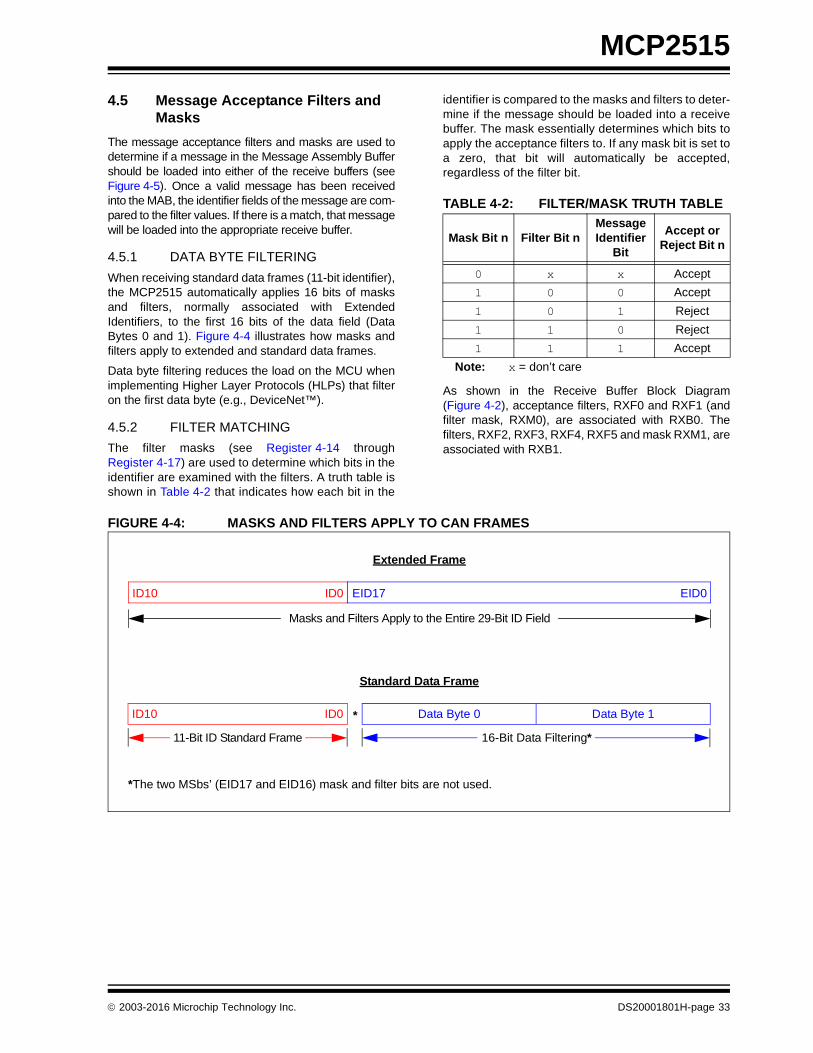
4.5 Message Acceptance Filters and Masks
The message acceptance filters and masks are used todetermine if a message in the Message Assembly Buffershould be loaded into either of the receive buffers (seeFigure 4-5). Once a valid message has been receivedinto the MAB, the identifier fields of the message are com-pared to the filter values. If there is a match, that messagewill be loaded into the appropriate receive buffer.
4.5.1 DATA BYTE FILTERING
When receiving standard data frames (11-bit identifier),the MCP2515 automatically applies 16 bits of masksand filters, normally associated with ExtendedIdentifiers, to the first 16 bits of the data field (DataBytes 0 and 1). Figure 4-4 illustrates how masks andfilters apply to extended and standard data frames.
Data byte filtering reduces the load on the MCU whenimplementing Higher Layer Protocols (HLPs) that filteron the first data byte (e.g., DeviceNet™).
4.5.2 FILTER MATCHING
The filter masks (see Register 4-14 throughRegister 4-17) are used to determine which bits in theidentifier are examined with the filters. A truth table isshown in Table 4-2 that indicates how each bit in the
identifier is compared to the masks and filters to deter-mine if the message should be loaded into a receivebuffer. The mask essentially determines which bits toapply the acceptance filters to. If any mask bit is set toa zero, that bit will automatically be accepted,regardless of the filter bit.
TABLE 4-2: FILTER/MASK TRUTH TABLE
As shown in the Receive Buffer Block Diagram(Figure 4-2), acceptance filters, RXF0 and RXF1 (andfilter mask, RXM0), are associated with RXB0. Thefilters, RXF2, RXF3, RXF4, RXF5 and mask RXM1, areassociated with RXB1.
FIGURE 4-4: MASKS AND FILTERS APPLY TO CAN FRAMES
Mask Bit n Filter Bit nMessage Identifier
Bit
Accept or Reject Bit n
0 x x Accept
1 0 0 Accept
1 0 1 Reject
1 1 0 Reject
1 1 1 Accept
Note: x = don’t care
Extended Frame
Standard Data Frame
ID10 ID0 EID17 EID0
Masks and Filters Apply to the Entire 29-Bit ID Field
ID10 ID0 Data Byte 0 Data Byte 1
11-Bit ID Standard Frame
*
16-Bit Data Filtering*
*The two MSbs’ (EID17 and EID16) mask and filter bits are not used.
2003-2016 Microchip Technology Inc. DS20001801H-page 33
MCP2515
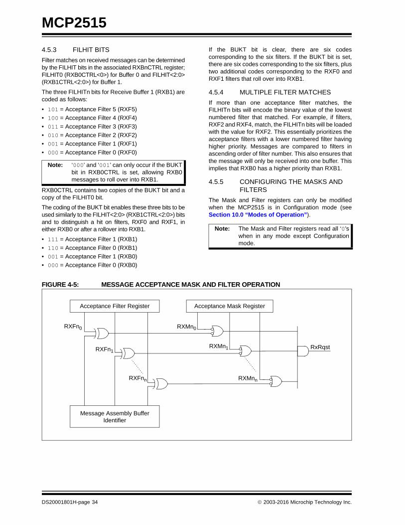
4.5.3 FILHIT BITS
Filter matches on received messages can be determinedby the FILHIT bits in the associated RXBnCTRL register;FILHIT0 (RXB0CTRL<0>) for Buffer 0 and FILHIT<2:0>(RXB1CTRL<2:0>) for Buffer 1.
The three FILHITn bits for Receive Buffer 1 (RXB1) arecoded as follows:
• 101 = Acceptance Filter 5 (RXF5)
• 100 = Acceptance Filter 4 (RXF4)
• 011 = Acceptance Filter 3 (RXF3)
• 010 = Acceptance Filter 2 (RXF2)
• 001 = Acceptance Filter 1 (RXF1)
• 000 = Acceptance Filter 0 (RXF0)
RXB0CTRL contains two copies of the BUKT bit and acopy of the FILHIT0 bit.
The coding of the BUKT bit enables these three bits to beused similarly to the FILHIT<2:0> (RXB1CTRL<2:0>) bitsand to distinguish a hit on filters, RXF0 and RXF1, ineither RXB0 or after a rollover into RXB1.
• 111 = Acceptance Filter 1 (RXB1)
• 110 = Acceptance Filter 0 (RXB1)
• 001 = Acceptance Filter 1 (RXB0)
• 000 = Acceptance Filter 0 (RXB0)
If the BUKT bit is clear, there are six codescorresponding to the six filters. If the BUKT bit is set,there are six codes corresponding to the six filters, plustwo additional codes corresponding to the RXF0 andRXF1 filters that roll over into RXB1.
4.5.4 MULTIPLE FILTER MATCHES
If more than one acceptance filter matches, theFILHITn bits will encode the binary value of the lowestnumbered filter that matched. For example, if filters,RXF2 and RXF4, match, the FILHITn bits will be loadedwith the value for RXF2. This essentially prioritizes theacceptance filters with a lower numbered filter havinghigher priority. Messages are compared to filters inascending order of filter number. This also ensures thatthe message will only be received into one buffer. Thisimplies that RXB0 has a higher priority than RXB1.
4.5.5 CONFIGURING THE MASKS AND FILTERS
The Mask and Filter registers can only be modifiedwhen the MCP2515 is in Configuration mode (seeSection 10.0 “Modes of Operation”).
FIGURE 4-5: MESSAGE ACCEPTANCE MASK AND FILTER OPERATION
Note: ‘000’ and ‘001’ can only occur if the BUKTbit in RXB0CTRL is set, allowing RXB0messages to roll over into RXB1.
Note: The Mask and Filter registers read all ‘0’swhen in any mode except Configurationmode.
Acceptance Mask Register
RxRqst
Message Assembly Buffer
RXFn0
RXFn1
RXFnn
RXMn0
RXMn1
RXMnn
Identifier
Acceptance Filter Register
DS20001801H-page 34 2003-2016 Microchip Technology Inc.

MCP2515
REGISTER 4-10: RXFnSIDH: FILTER n STANDARD IDENTIFIER REGISTER HIGH(ADDRESS: 00h, 04h, 08h, 10h, 14h, 18h)(1)
R/W-x R/W-x R/W-x R/W-x R/W-x R/W-x R/W-x R/W-x
SID10 SID9 SID8 SID7 SID6 SID5 SID4 SID3
bit 7 bit 0
Legend:
R = Readable bit W = Writable bit U = Unimplemented bit, read as ‘0’
-n = Value at POR ‘1’ = Bit is set ‘0’ = Bit is cleared x = Bit is unknown
bit 7-0 SID<10:3>: Standard Identifier Filter bits
These bits hold the filter bits to be applied to bits<10:3> of the Standard Identifier portion of a receivedmessage.
Note 1: The Mask and Filter registers read all ‘0’s when in any mode except Configuration mode.
REGISTER 4-11: RXFnSIDL: FILTER n STANDARD IDENTIFIER REGISTER LOW(ADDRESS: 01h, 05h, 09h, 11h, 15h, 19h)(1)
R/W-x R/W-x R/W-x U-0 R/W-x U-0 R/W-x R/W-x
SID2 SID1 SID0 — EXIDE — EID17 EID16
bit 7 bit 0
Legend:
R = Readable bit W = Writable bit U = Unimplemented bit, read as ‘0’
-n = Value at POR ‘1’ = Bit is set ‘0’ = Bit is cleared x = Bit is unknown
bit 7-5 SID<2:0>: Standard Identifier Filter bits
These bits hold the filter bits to be applied to bits<2:0> of the Standard Identifier portion of a receivedmessage.
bit 4 Unimplemented: Read as ‘0’
bit 3 EXIDE: Extended Identifier Enable bit
1 = Filter is applied only to extended frames0 = Filter is applied only to standard frames
bit 2 Unimplemented: Read as ‘0’
bit 1-0 EID<17:16>: Extended Identifier Filter bits
These bits hold the filter bits to be applied to bits<17:16> of the Extended Identifier portion of areceived message.
Note 1: The Mask and Filter registers read all ‘0’s when in any mode except Configuration mode.
2003-2016 Microchip Technology Inc. DS20001801H-page 35
MCP2515
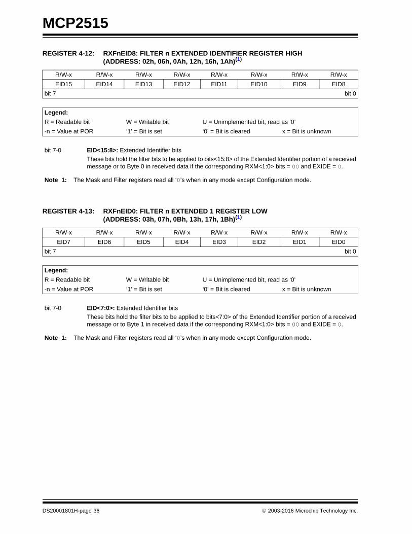
REGISTER 4-12: RXFnEID8: FILTER n EXTENDED IDENTIFIER REGISTER HIGH(ADDRESS: 02h, 06h, 0Ah, 12h, 16h, 1Ah)(1)
R/W-x R/W-x R/W-x R/W-x R/W-x R/W-x R/W-x R/W-x
EID15 EID14 EID13 EID12 EID11 EID10 EID9 EID8
bit 7 bit 0
Legend:
R = Readable bit W = Writable bit U = Unimplemented bit, read as ‘0’
-n = Value at POR ‘1’ = Bit is set ‘0’ = Bit is cleared x = Bit is unknown
bit 7-0 EID<15:8>: Extended Identifier bits
These bits hold the filter bits to be applied to bits<15:8> of the Extended Identifier portion of a receivedmessage or to Byte 0 in received data if the corresponding RXM<1:0> bits = 00 and EXIDE = 0.
Note 1: The Mask and Filter registers read all ‘0’s when in any mode except Configuration mode.
REGISTER 4-13: RXFnEID0: FILTER n EXTENDED 1 REGISTER LOW(ADDRESS: 03h, 07h, 0Bh, 13h, 17h, 1Bh)(1)
R/W-x R/W-x R/W-x R/W-x R/W-x R/W-x R/W-x R/W-x
EID7 EID6 EID5 EID4 EID3 EID2 EID1 EID0
bit 7 bit 0
Legend:
R = Readable bit W = Writable bit U = Unimplemented bit, read as ‘0’
-n = Value at POR ‘1’ = Bit is set ‘0’ = Bit is cleared x = Bit is unknown
bit 7-0 EID<7:0>: Extended Identifier bits
These bits hold the filter bits to be applied to bits<7:0> of the Extended Identifier portion of a receivedmessage or to Byte 1 in received data if the corresponding RXM<1:0> bits = 00 and EXIDE = 0.
Note 1: The Mask and Filter registers read all ‘0’s when in any mode except Configuration mode.
DS20001801H-page 36 2003-2016 Microchip Technology Inc.

MCP2515
REGISTER 4-14: RXMnSIDH: MASK n STANDARD IDENTIFIER REGISTER HIGH (ADDRESS: 20h, 24h)(1)
R/W-0 R/W-0 R/W-0 R/W-0 R/W-0 R/W-0 R/W-0 R/W-0
SID10 SID9 SID8 SID7 SID6 SID5 SID4 SID3
bit 7 bit 0
Legend:
R = Readable bit W = Writable bit U = Unimplemented bit, read as ‘0’
-n = Value at POR ‘1’ = Bit is set ‘0’ = Bit is cleared x = Bit is unknown
bit 7-0 SID<10:3>: Standard Identifier Mask bits
These bits hold the mask bits to be applied to bits<10:3> of the Standard Identifier portion of a receivedmessage.
Note 1: The Mask and Filter registers read all ‘0’s when in any mode except Configuration mode.
REGISTER 4-15: RXMnSIDL: MASK n STANDARD IDENTIFIER REGISTER LOW (ADDRESS: 21h, 25h)(1)
R/W-0 R/W-0 R/W-0 U-0 U-0 U-0 R/W-0 R/W-0
SID2 SID1 SID0 — — — EID17 EID16
bit 7 bit 0
Legend:
R = Readable bit W = Writable bit U = Unimplemented bit, read as ‘0’
-n = Value at POR ‘1’ = Bit is set ‘0’ = Bit is cleared x = Bit is unknown
bit 7-5 SID<2:0>: Standard Identifier Mask bits
These bits hold the mask bits to be applied to bits<2:0> of the Standard Identifier portion of a receivedmessage.
bit 4-2 Unimplemented: Reads as ‘0’
bit 1-0 EID<17:16>: Extended Identifier Mask bits
These bits hold the mask bits to be applied to bits<17:16> of the Extended Identifier portion of areceived message.
Note 1: The Mask and Filter registers read all ‘0’s when in any mode except Configuration mode.
2003-2016 Microchip Technology Inc. DS20001801H-page 37
MCP2515
\
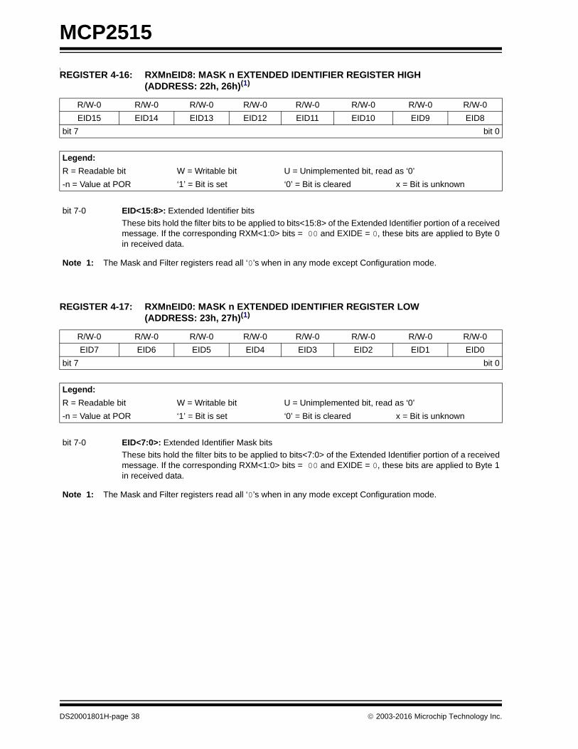
REGISTER 4-16: RXMnEID8: MASK n EXTENDED IDENTIFIER REGISTER HIGH (ADDRESS: 22h, 26h)(1)
R/W-0 R/W-0 R/W-0 R/W-0 R/W-0 R/W-0 R/W-0 R/W-0
EID15 EID14 EID13 EID12 EID11 EID10 EID9 EID8
bit 7 bit 0
Legend:
R = Readable bit W = Writable bit U = Unimplemented bit, read as ‘0’
-n = Value at POR ‘1’ = Bit is set ‘0’ = Bit is cleared x = Bit is unknown
bit 7-0 EID<15:8>: Extended Identifier bits
These bits hold the filter bits to be applied to bits<15:8> of the Extended Identifier portion of a receivedmessage. If the corresponding RXM<1:0> bits = 00 and EXIDE = 0, these bits are applied to Byte 0in received data.
Note 1: The Mask and Filter registers read all ‘0’s when in any mode except Configuration mode.
REGISTER 4-17: RXMnEID0: MASK n EXTENDED IDENTIFIER REGISTER LOW (ADDRESS: 23h, 27h)(1)
R/W-0 R/W-0 R/W-0 R/W-0 R/W-0 R/W-0 R/W-0 R/W-0
EID7 EID6 EID5 EID4 EID3 EID2 EID1 EID0
bit 7 bit 0
Legend:
R = Readable bit W = Writable bit U = Unimplemented bit, read as ‘0’
-n = Value at POR ‘1’ = Bit is set ‘0’ = Bit is cleared x = Bit is unknown
bit 7-0 EID<7:0>: Extended Identifier Mask bits
These bits hold the filter bits to be applied to bits<7:0> of the Extended Identifier portion of a receivedmessage. If the corresponding RXM<1:0> bits = 00 and EXIDE = 0, these bits are applied to Byte 1in received data.
Note 1: The Mask and Filter registers read all ‘0’s when in any mode except Configuration mode.
DS20001801H-page 38 2003-2016 Microchip Technology Inc.

MCP2515
5.0 BIT TIMING
All nodes on a given CAN bus must have the sameNominal Bit Rate (NBR). The CAN protocol uses Non-Return-to-Zero (NRZ) coding, which does not encode aclock within the data stream. Therefore, the receiveclock must be recovered by the receiving nodes andsynchronized to the transmitter’s clock.
As oscillators and transmission times may vary fromnode to node, the receiver must have some type ofPhase-Locked Loop (PLL) synchronized to datatransmission edges to synchronize and maintain thereceiver clock. Since the data is NRZ coded, it isnecessary to include bit-stuffing to ensure that an edgeoccurs, at least every six bit times, to maintain theDigital Phase-Locked Loop (DPLL) synchronization.
The bit timing of the MCP2515 is implemented using aDPLL that is configured to synchronize to the incomingdata, as well as provide the nominal timing for thetransmitted data. The DPLL breaks each bit time intomultiple segments made up of minimal periods of time,called the Time Quanta (TQ).
Bus timing functions executed within the bit time frame(such as synchronization to the local oscillator, networktransmission delay compensation and sample pointpositioning) are defined by the programmable BitTiming Logic (BTL) of the DPLL.
5.1 The CAN Bit Time
All devices on the CAN bus must use the same bit rate.However, all devices are not required to have the samemaster oscillator clock frequency. For the differentclock frequencies of the individual devices, the bit ratehas to be adjusted by appropriately setting the BaudRate Prescaler and number of Time Quanta in eachsegment.
The CAN bit time is made up of non-overlapping seg-ments. Each of these segments is made up of integerunits, called Time Quanta (TQ), explained later in thisdata sheet. The Nominal Bit Rate (NBR) is defined inthe CAN specification as the number of bits persecond, transmitted by an ideal transmitter, with noresynchronization. It can be described with theequation:
EQUATION 5-1:
5.2 Nominal Bit Time
The Nominal Bit Time (NBT) (tbit) is made up of non-overlapping segments (Figure 5-1). Therefore, theNBT is the summation of the following segments:
Associated with the NBT are the sample point,Synchronization Jump Width (SJW) and InformationProcessing Time (IPT), which are explained later.
5.2.1 SYNCHRONIZATION SEGMENT
The Synchronization Segment (SyncSeg) is the firstsegment in the NBT and is used to synchronize thenodes on the bus. Bit edges are expected to occurwithin the SyncSeg. This segment is fixed at 1 TQ.
FIGURE 5-1: CAN BIT TIME SEGMENTS
NBR fbit1
tbit-------= =
tbit tSyncSeg tPropSeg tPS1 tPS2+ + +=
Nominal Bit Time (NBT), tbit
SamplePoint
SyncSeg PropSeg PhaseSeg1 (PS1) PhaseSeg2 (PS2)
2003-2016 Microchip Technology Inc. DS20001801H-page 39

MCP2515
5.2.2 PROPAGATION SEGMENT
The Propagation Segment (PropSeg) exists tocompensate for physical delays between nodes. Thepropagation delay is defined as twice the sum of thesignal’s propagation time on the bus line, including thedelays associated with the bus driver. The PropSeg isprogrammable from 1-8 TQs.
5.2.3 PHASE SEGMENT 1 (PS1) AND PHASE SEGMENT 2 (PS2)
The two Phase Segments, PS1 and PS2, are used tocompensate for edge phase errors on the bus. PS1 canbe lengthened (or PS2 shortened) by resynchroniza-tion. PS1 is programmable from 1-8 TQs and PS2 isprogrammable from 2-8 TQs.
5.2.4 SAMPLE POINT
The sample point is the point in the bit time at which thelogic level is read and interpreted. The sample point islocated at the end of PS1. The exception to this rule isif the Sample mode is configured to sample three timesper bit. In this case, while the bit is still sampled at theend of PS1, two additional samples are taken at one-half TQ intervals prior to the end of PS1, with the valueof the bit being determined by a majority decision.
5.2.5 INFORMATION PROCESSING TIME
The Information Processing Time (IPT) is the timerequired for the logic to determine the bit level of asampled bit. The IPT begins at the sample point, ismeasured in TQ and is fixed at 2 TQs for the MicrochipCAN module. Since PS2 also begins at the samplepoint and is the last segment in the bit time, it isrequired that the PS2 minimum is not less than the IPT.
Therefore:
5.2.6 SYNCHRONIZATION JUMP WIDTH
The Synchronization Jump Width (SJW) adjusts the bitclock, as necessary, by 1-4 TQs (as configured) tomaintain synchronization with the transmittedmessage. Synchronization is covered in more detaillater in this data sheet.
5.3 Time Quantum
Each of the segments that make up a bit time are madeup of integer units, called Time Quanta (TQ). The lengthof each Time Quantum is based on the oscillator period(TOSC). The base TQ equals twice the oscillator period.Figure 5-2 shows how the bit period is derived fromTOSC and TQ. The TQ length equals one TQ clockperiod (tBRPCLK), which is programmable using a pro-grammable prescaler, called the Baud Rate Prescaler(BRP). This is illustrated in the following equation:
EQUATION 5-2:
FIGURE 5-2: TQ AND THE BIT PERIOD
PS2min = IPT = 2 TQs
Where: BRP equals the configuration as shownin Register 5-1.
TQ = 2 • BRP • TOSC =2 • BRP
FOSC
TOSC
TBRPCLK
tbitSync
(fixed)PropSeg
(Programmable)PS2
(Programmable)PS1
(Programmable)
TQ(tTQ)
CAN Bit Time
DS20001801H-page 40 2003-2016 Microchip Technology Inc.

MCP2515
5.4 Synchronization
To compensate for phase shifts between the oscillatorfrequencies of each of the nodes on the bus, each CANcontroller must be able to synchronize to the relevantsignal edge of the incoming signal. Synchronization isthe process by which the DPLL function is implemented.
When an edge in the transmitted data is detected, thelogic will compare the location of the edge to theexpected time (SyncSeg). The circuit will then adjustthe values of PS1 and PS2 as necessary.
There are two mechanisms used for synchronization:
1. Hard synchronization
2. Resynchronization
5.4.1 HARD SYNCHRONIZATION
Hard synchronization is only performed when there is arecessive-to-dominant edge during a Bus Idle condi-tion, indicating the start of a message. After hardsynchronization, the bit time counters are restarted withSyncSeg.
Hard synchronization forces the edge that hasoccurred to lie within the Synchronization Segment ofthe restarted bit time. Due to the rules of synchroniza-tion, if a hard synchronization occurs, there will not bea resynchronization within that bit time.
5.4.2 RESYNCHRONIZATION
As a result of resynchronization, PS1 may belengthened or PS2 may be shortened. The amount oflengthening or shortening of the Phase Buffer Seg-ments has an upper bound, given by theSynchronization Jump Width (SJW).
The value of the SJW will be added to PS1 orsubtracted from PS2 (see Figure 5-3). The SJWrepresents the loop filtering of the DPLL. The SJW isprogrammable between 1 TQ and 4 TQs.
5.4.2.1 Phase Errors
The NRZ bit coding method does not encode a clockinto the message. Clocking information will only bederived from recessive-to-dominant transitions. Theproperty which states that only a fixed maximumnumber of successive bits have the same value (bit-stuffing) ensures resynchronization to the bit streamduring a frame.
The phase error of an edge is given by the position ofthe edge relative to SyncSeg, measured in TQ. Thephase error is defined in a magnitude of TQ as follows:
• e = 0 if the edge lies within SyncSeg
• e > 0 if the edge lies before the sample point (TQ is added to PS1)
• e < 0 if the edge lies after the sample point of the previous bit (TQ is subtracted from PS2)
5.4.2.2 No Phase Error (e = 0)
If the magnitude of the phase error is less than or equalto the programmed value of the SJW, the effect of aresynchronization is the same as that of a hardsynchronization.
5.4.2.3 Positive Phase Error (e > 0)
If the magnitude of the phase error is larger than theSJW, and if the phase error is positive, PS1 islengthened by an amount equal to the SJW.
5.4.2.4 Negative Phase Error (e < 0)
If the magnitude of the phase error is larger than theresynchronization jump width, and the phase error isnegative, PS2 is shortened by an amount equal to theSJW.
5.4.3 SYNCHRONIZATION RULES
1. Only recessive-to-dominant edges will be usedfor synchronization.
2. Only one synchronization within one bit time isallowed.
3. An edge will be used for synchronization only ifthe value detected at the previous sample point(previously read bus value) differs from the busvalue immediately after the edge.
4. A transmitting node will not resynchronize on apositive phase error (e > 0).
5. If the absolute magnitude of the phase error isgreater than the SJW, the appropriate PhaseSegment will adjust by an amount equal to theSJW.
2003-2016 Microchip Technology Inc. DS20001801H-page 41
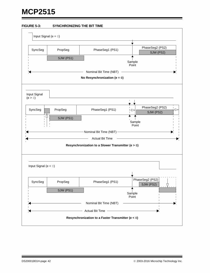
MCP2515
FIGURE 5-3: SYNCHRONIZING THE BIT TIME
SyncSeg PropSeg PhaseSeg1 (PS1)PhaseSeg2 (PS2)
SamplePoint
SyncSeg PropSeg PhaseSeg1 (PS1)PhaseSeg2 (PS2)
SamplePoint
SyncSeg PropSeg PhaseSeg1 (PS1)PhaseSeg2 (PS2)
SamplePoint
Nominal Bit Time (NBT)
SJW (PS1)
SJW (PS2)
Nominal Bit Time (NBT)
SJW (PS1)
SJW (PS2)
Actual Bit Time
Resynchronization to a Slower Transmitter (e > 0)
Input Signal
Input Signal (e < 0)
SJW (PS1)
SJW (PS2)
Nominal Bit Time (NBT)
Actual Bit Time
Resynchronization to a Faster Transmitter (e < 0)
Input Signal (e = 0)
No Resynchronization (e = 0)
(e > 0)
DS20001801H-page 42 2003-2016 Microchip Technology Inc.

MCP2515
5.5 Programming Time Segments
Some requirements for programming of the TimeSegments:
• PropSeg + PS1 PS2
• PropSeg + PS1 TDELAY
• PS2 > SJW
For example, assuming that a 125 kHz CAN baud ratewith FOSC = 20 MHz is desired:
TOSC = 50 ns, choose BRP<5:0> = 04h, then TQ = 500 ns.To obtain 125 kHz, the bit time must be 16 TQs.
Typically, the sampling of the bit should take place atabout 60-70% of the bit time, depending on the systemparameters. Also, typically, the TDELAY is 1-2 TQs.
SyncSeg = 1 TQ and PropSeg = 2 TQs. So settingPS1 = 7 TQs would place the sample at 10 TQs after thetransition. This would leave 6 TQs for PS2.
Since PS2 is 6, according to the rules, SJW could be amaximum of 4 TQs. However, a large SJW is typicallyonly necessary when the clock generation of the differ-ent nodes is inaccurate or unstable, such as usingceramic resonators. So a SJW of 1 is usually enough.
5.6 Oscillator Tolerance
The bit timing requirements allow ceramic resonatorsto be used in applications with transmission rates of upto 125 kbit/sec as a rule of thumb. For the full busspeed range of the CAN protocol, a quartz oscillator isrequired. A maximum node-to-node oscillator variationof 1.7% is allowed.
5.7 Bit Timing Configuration Registers
The Configuration registers (CNF1, CNF2, CNF3)control the bit timing for the CAN bus interface. Theseregisters can only be modified when the MCP2515 is inConfiguration mode (see Section 10.0 “Modes ofOperation”).
5.7.1 CNF1
The BRP<5:0> bits control the Baud Rate Prescaler.These bits set the length of TQ relative to the OSC1input frequency, with the minimum TQ length being2 TOSC (when BRP<5:0> = b000000). The SJW<1:0>bits select the SJW in terms of number of TQs.
5.7.2 CNF2
The PRSEG<2:0> bits set the length (in TQs) of thePropagation Segment. The PHSEG1<2:0> bits set thelength (in TQs) of PS1.
The SAM bit controls how many times the RXCAN pinis sampled. Setting this bit to a ‘1’ causes the bus to besampled three times: twice at TQ/2 before the samplepoint and once at the normal sample point (which is atthe end of PS1). The value of the bus is determined tobe the majority sampled. If the SAM bit is set to a ‘0’,the RXCAN pin is sampled only once at the samplepoint.
The BTLMODE bit controls how the length of PS2 isdetermined. If this bit is set to a ‘1’, the length of PS2 isdetermined by the PHSEG2<2:0> bits of CNF3 (seeSection 5.7.3 “CNF3”). If the BTLMODE bit is set to a‘0’, the length of PS2 is greater than that of PS1 and theInformation Processing Time (which is fixed at 2 TQsfor the MCP2515).
5.7.3 CNF3
The PHSEG2<2:0> bits set the length (in TQs) of PS2if the BTLMODE bit (CNF2<7>) is set to a ‘1’. If theBTLMODE bit is set to a ‘0’, the PHSEG2<2:0> bitshave no effect.
2003-2016 Microchip Technology Inc. DS20001801H-page 43
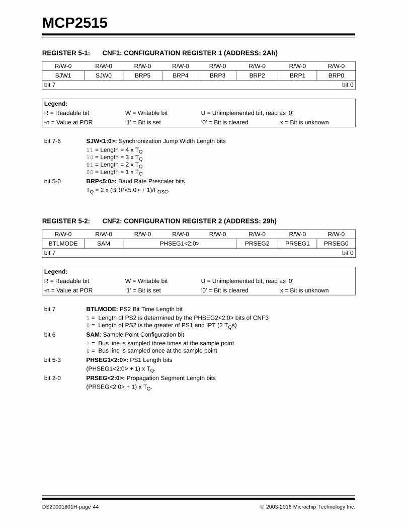
MCP2515
REGISTER 5-1: CNF1: CONFIGURATION REGISTER 1 (ADDRESS: 2Ah)
R/W-0 R/W-0 R/W-0 R/W-0 R/W-0 R/W-0 R/W-0 R/W-0
SJW1 SJW0 BRP5 BRP4 BRP3 BRP2 BRP1 BRP0
bit 7 bit 0
Legend:
R = Readable bit W = Writable bit U = Unimplemented bit, read as ‘0’
-n = Value at POR ‘1’ = Bit is set ‘0’ = Bit is cleared x = Bit is unknown
bit 7-6 SJW<1:0>: Synchronization Jump Width Length bits
11 = Length = 4 x TQ10 = Length = 3 x TQ01 = Length = 2 x TQ00 = Length = 1 x TQ
bit 5-0 BRP<5:0>: Baud Rate Prescaler bits
TQ = 2 x (BRP<5:0> + 1)/FOSC.
REGISTER 5-2: CNF2: CONFIGURATION REGISTER 2 (ADDRESS: 29h)
R/W-0 R/W-0 R/W-0 R/W-0 R/W-0 R/W-0 R/W-0 R/W-0
BTLMODE SAM PHSEG1<2:0> PRSEG2 PRSEG1 PRSEG0
bit 7 bit 0
Legend:
R = Readable bit W = Writable bit U = Unimplemented bit, read as ‘0’
-n = Value at POR ‘1’ = Bit is set ‘0’ = Bit is cleared x = Bit is unknown
bit 7 BTLMODE: PS2 Bit Time Length bit
1 = Length of PS2 is determined by the PHSEG2<2:0> bits of CNF30 = Length of PS2 is the greater of PS1 and IPT (2 TQs)
bit 6 SAM: Sample Point Configuration bit
1 = Bus line is sampled three times at the sample point0 = Bus line is sampled once at the sample point
bit 5-3 PHSEG1<2:0>: PS1 Length bits
(PHSEG1<2:0> + 1) x TQ.
bit 2-0 PRSEG<2:0>: Propagation Segment Length bits
(PRSEG<2:0> + 1) x TQ.
DS20001801H-page 44 2003-2016 Microchip Technology Inc.

MCP2515
REGISTER 5-3: CNF3: CONFIGURATION REGISTER 3 (ADDRESS: 28h)
R/W-0 R/W-0 U-0 U-0 U-0 R/W-0 R/W-0 R/W-0
SOF WAKFIL — — — PHSEG2<2:0>
bit 7 bit 0
Legend:
R = Readable bit W = Writable bit U = Unimplemented bit, read as ‘0’
-n = Value at POR ‘1’ = Bit is set ‘0’ = Bit is cleared x = Bit is unknown
bit 7 SOF: Start-of-Frame signal bit
If CLKEN (CANCTRL<2>) = 1:1 = CLKOUT pin is enabled for SOF signal0 = CLKOUT pin is enabled for clock out function
If CLKEN (CANCTRL<2>) = 0:Bit is don’t care.
bit 6 WAKFIL: Wake-up Filter bit
1 = Wake-up filter is enabled0 = Wake-up filter is disabled
bit 5-3 Unimplemented: Reads as ‘0’
bit 2-0 PHSEG2<2:0>: PS2 Length bits
(PHSEG2<2:0> + 1) x TQ. Minimum valid setting for PS2 is 2 TQs.
2003-2016 Microchip Technology Inc. DS20001801H-page 45

MCP2515
NOTES:
DS20001801H-page 46 2003-2016 Microchip Technology Inc.

MCP2515
6.0 ERROR DETECTION
The CAN protocol provides sophisticated errordetection mechanisms. The following errors can bedetected.
6.1 CRC Error
With the Cyclic Redundancy Check (CRC), thetransmitter calculates special check bits for the bitsequence from the Start-of-Frame until the end of thedata field. This CRC sequence is transmitted in theCRC field. The receiving node also calculates the CRCsequence using the same formula and performs a com-parison to the received sequence. If a mismatch isdetected, a CRC error has occurred and an error frameis generated. The message is repeated.
6.2 Acknowledge Error
In the Acknowledge field of a message, the transmitterchecks if the Acknowledge Slot bit (which has beensent out as a recessive bit) contains a dominant bit. Ifnot, no other node has received the frame correctly. AnAcknowledge error has occurred, an error frame isgenerated and the message will have to be repeated.
6.3 Form Error
If a node detects a dominant bit in one of the foursegments (including End-of-Frame, interframe space,Acknowledge delimiter or CRC delimiter), a form errorhas occurred and an error frame is generated. Themessage is repeated.
6.4 Bit Error
A bit error occurs if a transmitter detects the oppositebit level to what it transmitted (i.e., transmitted adominant and detected a recessive, or transmitted arecessive and detected a dominant).
Exception: In the case where the transmitter sends arecessive bit, and a dominant bit is detected during thearbitration field and the Acknowledge Slot, no bit erroris generated because normal arbitration is occurring.
6.5 Stuff Error
lf, between the Start-of-Frame and the CRC delimiter,six consecutive bits with the same polarity aredetected, the bit-stuffing rule has been violated. A stufferror occurs and an error frame is generated. Themessage is repeated.
6.6 Error States
Detected errors are made known to all other nodes viaerror frames. The transmission of the erroneous mes-sage is aborted and the frame is repeated as soon aspossible. Furthermore, each CAN node is in one of thethree error states according to the value of the internalerror counters:
1. Error-active
2. Error-passive
3. Bus-off (transmitter only)
The error-active state is the usual state where the nodecan transmit messages and active error frames (madeof dominant bits) without any restrictions.
In the error-passive state, messages and passive errorframes (made of recessive bits) may be transmitted.
The bus-off state makes it temporarily impossible forthe station to participate in the bus communication.During this state, messages can neither be received ortransmitted. Only transmitters can go bus-off.
6.7 Error Modes and Error Counters
The MCP2515 contains two error counters: theReceive Error Counter (REC) (see Register 6-2) andthe Transmit Error Counter (TEC) (see Register 6-1).The values of both counters can be read by the MCU.These counters are incremented/decremented inaccordance with the CAN bus specification.
The MCP2515 is error-active if both error counters arebelow the error-passive limit of 128.
It is error-passive if at least one of the error countersequals or exceeds 128.
It goes to bus-off if the TEC exceeds the bus-off limit of255. The device remains in this state until the bus-offrecovery sequence is received. The bus-off recoverysequence consists of 128 occurrences of 11 consecutiverecessive bits (see Figure 6-1).
The current Error mode of the MCP2515 can be readby the MCU via the EFLG register (see Register 6-3).
Additionally, there is an error state warning flag bit,EWARN (EFLG<0>), which is set if at least one of theerror counters equals or exceeds the error warning limitof 96. EWARN is reset if both error counters are lessthan the error warning limit.
Note: The MCP2515, after going bus-off, willrecover back to error-active without anyintervention by the MCU if the busremains idle for 128 x 11 bit times. If this isnot desired, the error Interrupt ServiceRoutine (ISR) should address this.
2003-2016 Microchip Technology Inc. DS20001801H-page 47

MCP2515
FIGURE 6-1: ERROR MODES STATE DIAGRAM
Bus-Off
Error-Active
Error-Passive
REC < 127 orTEC < 127
REC > 127 orTEC > 127
TEC > 255
Reset
128 Occurrences of11 Consecutive“Recessive” Bits
DS20001801H-page 48 2003-2016 Microchip Technology Inc.

MCP2515
REGISTER 6-1: TEC: TRANSMIT ERROR COUNTER REGISTER (ADDRESS: 1Ch)
R-0 R-0 R-0 R-0 R-0 R-0 R-0 R-0
TEC7 TEC6 TEC5 TEC4 TEC3 TEC2 TEC1 TEC0
bit 7 bit 0
Legend:
R = Readable bit W = Writable bit U = Unimplemented bit, read as ‘0’
-n = Value at POR ‘1’ = Bit is set ‘0’ = Bit is cleared x = Bit is unknown
bit 7-0 TEC<7:0>: Transmit Error Count bits
REGISTER 6-2: REC: RECEIVE ERROR COUNTER REGISTER (ADDRESS: 1Dh)
R-0 R-0 R-0 R-0 R-0 R-0 R-0 R-0
REC7 REC6 REC5 REC4 REC3 REC2 REC1 REC0
bit 7 bit 0
Legend:
R = Readable bit W = Writable bit U = Unimplemented bit, read as ‘0’
-n = Value at POR ‘1’ = Bit is set ‘0’ = Bit is cleared x = Bit is unknown
bit 7-0 REC<7:0>: Receive Error Count bits
2003-2016 Microchip Technology Inc. DS20001801H-page 49
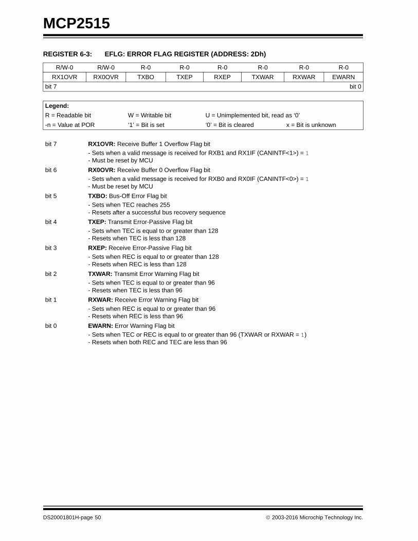
MCP2515
REGISTER 6-3: EFLG: ERROR FLAG REGISTER (ADDRESS: 2Dh)
R/W-0 R/W-0 R-0 R-0 R-0 R-0 R-0 R-0
RX1OVR RX0OVR TXBO TXEP RXEP TXWAR RXWAR EWARN
bit 7 bit 0
Legend:
R = Readable bit W = Writable bit U = Unimplemented bit, read as ‘0’
-n = Value at POR ‘1’ = Bit is set ‘0’ = Bit is cleared x = Bit is unknown
bit 7 RX1OVR: Receive Buffer 1 Overflow Flag bit
- Sets when a valid message is received for RXB1 and RX1IF (CANINTF<1>) = 1- Must be reset by MCU
bit 6 RX0OVR: Receive Buffer 0 Overflow Flag bit
- Sets when a valid message is received for RXB0 and RX0IF (CANINTF<0>) = 1- Must be reset by MCU
bit 5 TXBO: Bus-Off Error Flag bit
- Sets when TEC reaches 255- Resets after a successful bus recovery sequence
bit 4 TXEP: Transmit Error-Passive Flag bit
- Sets when TEC is equal to or greater than 128- Resets when TEC is less than 128
bit 3 RXEP: Receive Error-Passive Flag bit
- Sets when REC is equal to or greater than 128- Resets when REC is less than 128
bit 2 TXWAR: Transmit Error Warning Flag bit
- Sets when TEC is equal to or greater than 96- Resets when TEC is less than 96
bit 1 RXWAR: Receive Error Warning Flag bit
- Sets when REC is equal to or greater than 96- Resets when REC is less than 96
bit 0 EWARN: Error Warning Flag bit
- Sets when TEC or REC is equal to or greater than 96 (TXWAR or RXWAR = 1)- Resets when both REC and TEC are less than 96
DS20001801H-page 50 2003-2016 Microchip Technology Inc.
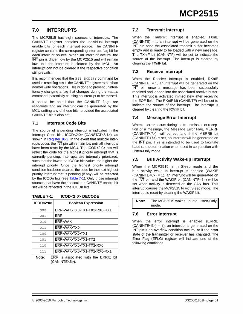
MCP2515
7.0 INTERRUPTS
The MCP2515 has eight sources of interrupts. TheCANINTE register contains the individual interruptenable bits for each interrupt source. The CANINTFregister contains the corresponding interrupt flag bit foreach interrupt source. When an interrupt occurs, theINT pin is driven low by the MCP2515 and will remainlow until the interrupt is cleared by the MCU. Aninterrupt can not be cleared if the respective conditionstill prevails.
It is recommended that the BIT MODIFY command beused to reset flag bits in the CANINTF register rather thannormal write operations. This is done to prevent uninten-tionally changing a flag that changes during the WRITEcommand, potentially causing an interrupt to be missed.
It should be noted that the CANINTF flags areread/write and an interrupt can be generated by theMCU setting any of these bits, provided the associatedCANINTE bit is also set.
7.1 Interrupt Code Bits
The source of a pending interrupt is indicated in theInterrupt Code bits, ICOD<2:0> (CANSTAT<3:1>), asshown in Register 10-2. In the event that multiple inter-rupts occur, the INT pin will remain low until all interruptshave been reset by the MCU. The ICOD<2:0> bits willreflect the code for the highest priority interrupt that iscurrently pending. Interrupts are internally prioritized,such that the lower the ICODn bits value, the higher theinterrupt priority. Once the highest priority interruptcondition has been cleared, the code for the next highestpriority interrupt that is pending (if any) will be reflectedby the ICODn bits (see Table 7-1). Only those interruptsources that have their associated CANINTE enable bitset will be reflected in the ICODn bits.
TABLE 7-1: ICOD<2:0> DECODE
7.2 Transmit Interrupt
When the Transmit Interrupt is enabled, TXnIE(CANINTE) = 1, an interrupt will be generated on theINT pin once the associated transmit buffer becomesempty and is ready to be loaded with a new message.The TXnIF bit (CANINTF) will be set to indicate thesource of the interrupt. The interrupt is cleared byclearing the TXnIF bit.
7.3 Receive Interrupt
When the Receive Interrupt is enabled, RXnIE(CANINTE) = 1, an interrupt will be generated on theINT pin once a message has been successfullyreceived and loaded into the associated receive buffer.This interrupt is activated immediately after receivingthe EOF field. The RXnIF bit (CANINTF) will be set toindicate the source of the interrupt. The interrupt iscleared by clearing the RXnIF bit.
7.4 Message Error Interrupt
When an error occurs during the transmission or recep-tion of a message, the Message Error Flag, MERRF(CANINTF<7>), will be set, and if the MERRE bit(CANINTE<7>) is set, an interrupt will be generated onthe INT pin. This is intended to be used to facilitatebaud rate determination when used in conjunction withListen-Only mode.
7.5 Bus Activity Wake-up Interrupt
When the MCP2515 is in Sleep mode and thebus activity wake-up interrupt is enabled (WAKIE(CANINTE<6>) = 1), an interrupt will be generated onthe INT pin and the WAKIF bit (CANINTF<6>) will beset when activity is detected on the CAN bus. Thisinterrupt causes the MCP2515 to exit Sleep mode. Theinterrupt is reset by clearing the WAKIF bit.
7.6 Error Interrupt
When the error interrupt is enabled (ERRIE(CANINTE<5>) = 1), an interrupt is generated on theINT pin if an overflow condition occurs, or if the errorstate of the transmitter or receiver has changed. TheError Flag (EFLG) register will indicate one of thefollowing conditions.
ICOD<2:0> Boolean Expression
000 ERR•WAK•TX0•TX1•TX2•RX0•RX1
001 ERR
010 ERR•WAK
011 ERR•WAK•TX0
100 ERR•WAK•TX0•TX1
101 ERR•WAK•TX0•TX1•TX2
110 ERR•WAK•TX0•TX1•TX2•RX0
111 ERR•WAK•TX0•TX1•TX2•RX0•RX1
Note: ERR is associated with the ERRIE bit(CANINTE<5>).
Note: The MCP2515 wakes up into Listen-Onlymode.
2003-2016 Microchip Technology Inc. DS20001801H-page 51
MCP2515
7.6.1 RECEIVER OVERFLOW
An overflow condition occurs when the MAB hasassembled a valid receive message (the messagemeets the criteria of the acceptance filters) and thereceive buffer associated with the filter is not availablefor loading of a new message. The associatedRXnOVR bit (EFLG) will be set to indicate the overflowcondition. This bit must be cleared by the MCU.
7.6.2 RECEIVER WARNING
The REC has reached the MCU warning limit of 96.
7.6.3 TRANSMITTER WARNING
The TEC has reached the MCU warning limit of 96.
7.6.4 RECEIVER ERROR-PASSIVE
The REC has exceeded the error-passive limit of 127and the device has gone to the error-passive state.
7.6.5 TRANSMITTER ERROR-PASSIVE
The TEC has exceeded the error-passive limit of 127and the device has gone to the error-passive state.
7.6.6 BUS-OFF
The TEC has exceeded 255 and the device has goneto the bus-off state.
7.7 Interrupt Acknowledge
Interrupts are directly associated with one or morestatus flags in the CANINTF register. Interrupts arepending as long as one of the flags is set. Once aninterrupt flag is set by the device, the flag can not bereset by the MCU until the interrupt condition isremoved.
DS20001801H-page 52 2003-2016 Microchip Technology Inc.
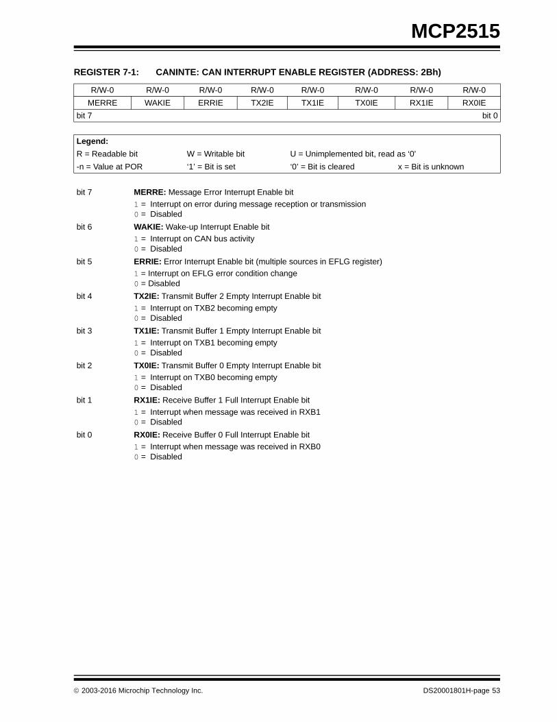
MCP2515
REGISTER 7-1: CANINTE: CAN INTERRUPT ENABLE REGISTER (ADDRESS: 2Bh)
R/W-0 R/W-0 R/W-0 R/W-0 R/W-0 R/W-0 R/W-0 R/W-0
MERRE WAKIE ERRIE TX2IE TX1IE TX0IE RX1IE RX0IE
bit 7 bit 0
Legend:
R = Readable bit W = Writable bit U = Unimplemented bit, read as ‘0’
-n = Value at POR ‘1’ = Bit is set ‘0’ = Bit is cleared x = Bit is unknown
bit 7 MERRE: Message Error Interrupt Enable bit
1 = Interrupt on error during message reception or transmission0 = Disabled
bit 6 WAKIE: Wake-up Interrupt Enable bit
1 = Interrupt on CAN bus activity0 = Disabled
bit 5 ERRIE: Error Interrupt Enable bit (multiple sources in EFLG register)
1 = Interrupt on EFLG error condition change0 = Disabled
bit 4 TX2IE: Transmit Buffer 2 Empty Interrupt Enable bit
1 = Interrupt on TXB2 becoming empty0 = Disabled
bit 3 TX1IE: Transmit Buffer 1 Empty Interrupt Enable bit
1 = Interrupt on TXB1 becoming empty0 = Disabled
bit 2 TX0IE: Transmit Buffer 0 Empty Interrupt Enable bit
1 = Interrupt on TXB0 becoming empty0 = Disabled
bit 1 RX1IE: Receive Buffer 1 Full Interrupt Enable bit
1 = Interrupt when message was received in RXB10 = Disabled
bit 0 RX0IE: Receive Buffer 0 Full Interrupt Enable bit
1 = Interrupt when message was received in RXB00 = Disabled
2003-2016 Microchip Technology Inc. DS20001801H-page 53

MCP2515
REGISTER 7-2: CANINTF: CAN INTERRUPT FLAG REGISTER (ADDRESS: 2Ch)
R/W-0 R/W-0 R/W-0 R/W-0 R/W-0 R/W-0 R/W-0 R/W-0
MERRF WAKIF ERRIF TX2IF TX1IF TX0IF RX1IF RX0IF
bit 7 bit 0
Legend:
R = Readable bit W = Writable bit U = Unimplemented bit, read as ‘0’
-n = Value at POR ‘1’ = Bit is set ‘0’ = Bit is cleared x = Bit is unknown
bit 7 MERRF: Message Error Interrupt Flag bit
1 = Interrupt is pending (must be cleared by MCU to reset the interrupt condition)0 = No interrupt is pending
bit 6 WAKIF: Wake-up Interrupt Flag bit
1 = Interrupt is pending (must be cleared by MCU to reset the interrupt condition)0 = No interrupt is pending
bit 5 ERRIF: Error Interrupt Flag bit (multiple sources in EFLG register)
1 = Interrupt is pending (must be cleared by MCU to reset the interrupt condition)0 = No interrupt is pending
bit 4 TX2IF: Transmit Buffer 2 Empty Interrupt Flag bit
1 = Interrupt is pending (must be cleared by MCU to reset the interrupt condition)0 = No interrupt is pending
bit 3 TX1IF: Transmit Buffer 1 Empty Interrupt Flag bit
1 = Interrupt is pending (must be cleared by MCU to reset the interrupt condition)0 = No interrupt is pending
bit 2 TX0IF: Transmit Buffer 0 Empty Interrupt Flag bit
1 = Interrupt is pending (must be cleared by MCU to reset the interrupt condition)0 = No interrupt is pending
bit 1 RX1IF: Receive Buffer 1 Full Interrupt Flag bit
1 = Interrupt is pending (must be cleared by MCU to reset the interrupt condition)0 = No interrupt is pending
bit 0 RX0IF: Receive Buffer 0 Full Interrupt Flag bit
1 = Interrupt is pending (must be cleared by MCU to reset the interrupt condition)0 = No interrupt is pending
DS20001801H-page 54 2003-2016 Microchip Technology Inc.
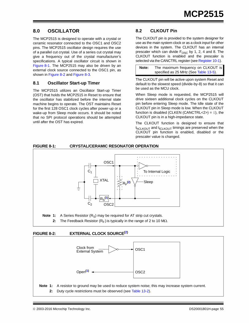
MCP2515
8.0 OSCILLATOR
The MCP2515 is designed to operate with a crystal orceramic resonator connected to the OSC1 and OSC2pins. The MCP2515 oscillator design requires the useof a parallel cut crystal. Use of a series cut crystal maygive a frequency out of the crystal manufacturer’sspecifications. A typical oscillator circuit is shown inFigure 8-1. The MCP2515 may also be driven by anexternal clock source connected to the OSC1 pin, asshown in Figure 8-2 and Figure 8-3.
8.1 Oscillator Start-up Timer
The MCP2515 utilizes an Oscillator Start-up Timer(OST) that holds the MCP2515 in Reset to ensure thatthe oscillator has stabilized before the internal statemachine begins to operate. The OST maintains Resetfor the first 128 OSC1 clock cycles after power-up or awake-up from Sleep mode occurs. It should be notedthat no SPI protocol operations should be attempteduntil after the OST has expired.
8.2 CLKOUT Pin
The CLKOUT pin is provided to the system designer foruse as the main system clock or as a clock input for otherdevices in the system. The CLKOUT has an internalprescaler which can divide FOSC by 1, 2, 4 and 8. TheCLKOUT function is enabled and the prescaler isselected via the CANCTRL register (see Register 10-1).
The CLKOUT pin will be active upon system Reset anddefault to the slowest speed (divide-by-8) so that it canbe used as the MCU clock.
When Sleep mode is requested, the MCP2515 willdrive sixteen additional clock cycles on the CLKOUTpin before entering Sleep mode. The Idle state of theCLKOUT pin in Sleep mode is low. When the CLKOUTfunction is disabled (CLKEN (CANCTRL<2>) = 0), theCLKOUT pin is in a high-impedance state.
The CLKOUT function is designed to ensure thatthCLKOUT and tlCLKOUT timings are preserved when theCLKOUT pin function is enabled, disabled or theprescaler value is changed.
FIGURE 8-1: CRYSTAL/CERAMIC RESONATOR OPERATION
FIGURE 8-2: EXTERNAL CLOCK SOURCE(2)
Note: The maximum frequency on CLKOUT isspecified as 25 MHz (See Table 13-5).
C1
C2
XTAL
OSC2
OSC1
Sleep
To Internal Logic
Note 1: A Series Resistor (RS) may be required for AT strip cut crystals.
2: The Feedback Resistor (RF) is typically in the range of 2 to 10 M.
RS(1)
RF(2)
Clock fromExternal System OSC1
OSC2
Note 1: A resistor to ground may be used to reduce system noise; this may increase system current.
2: Duty cycle restrictions must be observed (see Table 13-2).
Open(1)
2003-2016 Microchip Technology Inc. DS20001801H-page 55
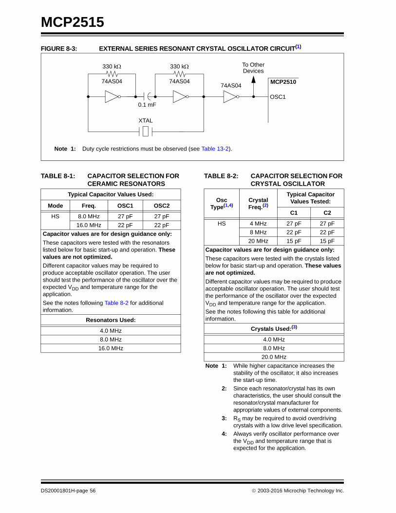
MCP2515
FIGURE 8-3: EXTERNAL SERIES RESONANT CRYSTAL OSCILLATOR CIRCUIT(1)
TABLE 8-1: CAPACITOR SELECTION FOR CERAMIC RESONATORS
TABLE 8-2: CAPACITOR SELECTION FOR CRYSTAL OSCILLATOR
330 k
74AS0474AS04
MCP2510
OSC1
To OtherDevices
XTAL
330 k
74AS04
0.1 mF
Note 1: Duty cycle restrictions must be observed (see Table 13-2).
Typical Capacitor Values Used:
Mode Freq. OSC1 OSC2
HS 8.0 MHz 27 pF 27 pF
16.0 MHz 22 pF 22 pF
Capacitor values are for design guidance only:
These capacitors were tested with the resonators listed below for basic start-up and operation. These values are not optimized.
Different capacitor values may be required to produce acceptable oscillator operation. The user should test the performance of the oscillator over the expected VDD and temperature range for the application.
See the notes following Table 8-2 for additional information.
Resonators Used:
4.0 MHz
8.0 MHz
16.0 MHz
Osc Type(1,4)
CrystalFreq.(2)
Typical Capacitor Values Tested:
C1 C2
HS 4 MHz 27 pF 27 pF
8 MHz 22 pF 22 pF
20 MHz 15 pF 15 pF
Capacitor values are for design guidance only:
These capacitors were tested with the crystals listed below for basic start-up and operation. These values are not optimized.
Different capacitor values may be required to produce acceptable oscillator operation. The user should test the performance of the oscillator over the expected VDD and temperature range for the application.
See the notes following this table for additional information.
Crystals Used:(3)
4.0 MHz
8.0 MHz
20.0 MHz
Note 1: While higher capacitance increases the stability of the oscillator, it also increases the start-up time.
2: Since each resonator/crystal has its own characteristics, the user should consult the resonator/crystal manufacturer for appropriate values of external components.
3: RS may be required to avoid overdriving crystals with a low drive level specification.
4: Always verify oscillator performance over the VDD and temperature range that is expected for the application.
DS20001801H-page 56 2003-2016 Microchip Technology Inc.
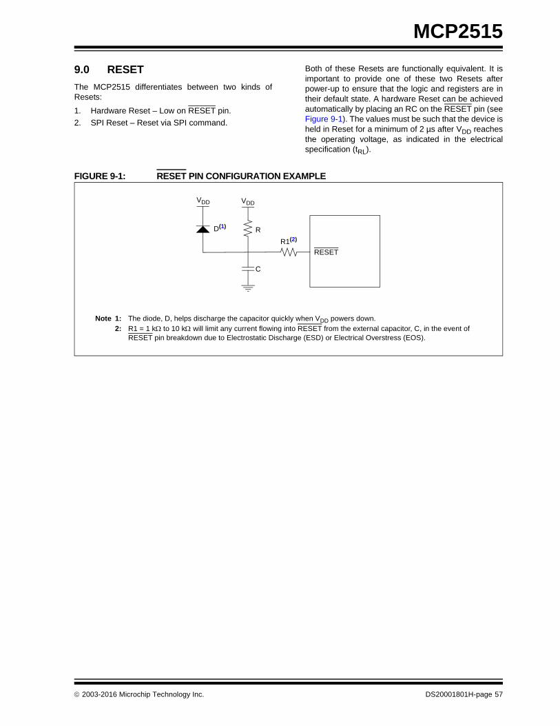
MCP2515
9.0 RESET
The MCP2515 differentiates between two kinds ofResets:
1. Hardware Reset – Low on RESET pin.
2. SPI Reset – Reset via SPI command.
Both of these Resets are functionally equivalent. It isimportant to provide one of these two Resets afterpower-up to ensure that the logic and registers are intheir default state. A hardware Reset can be achievedautomatically by placing an RC on the RESET pin (seeFigure 9-1). The values must be such that the device isheld in Reset for a minimum of 2 µs after VDD reachesthe operating voltage, as indicated in the electricalspecification (tRL).
FIGURE 9-1: RESET PIN CONFIGURATION EXAMPLE
RESET
VDDVDD
R
C
Note 1: The diode, D, helps discharge the capacitor quickly when VDD powers down.2: R1 = 1 k to 10 k will limit any current flowing into RESET from the external capacitor, C, in the event of
RESET pin breakdown due to Electrostatic Discharge (ESD) or Electrical Overstress (EOS).
R1(2)
D(1)
2003-2016 Microchip Technology Inc. DS20001801H-page 57

MCP2515
NOTES:
DS20001801H-page 58 2003-2016 Microchip Technology Inc.
MCP2515
10.0 MODES OF OPERATION
The MCP2515 has five modes of operation. Thesemodes are:
1. Configuration mode
2. Normal mode
3. Sleep mode
4. Listen-Only mode
5. Loopback mode
The operational mode is selected via theREQOP<2:0> bits (CANCTRL<7:5>); see Register 10-1).
When changing modes, the mode will not actuallychange until all pending message transmissions arecomplete. The requested mode must be verified byreading the OPMODE<2:0> bits (CANSTAT<7:5>);see Register 10-2.
10.1 Configuration Mode
The MCP2515 must be initialized before activation.This is only possible if the device is in the Configurationmode. Configuration mode is automatically selectedafter power-up, a Reset or can be entered from anyother mode by setting the REQOP<2:0> bits to ‘100’.When Configuration mode is entered, all error countersare cleared. Configuration mode is the only modewhere the following registers are modifiable:
• CNF1, CNF2, CNF3 registers
• TXRTSCTRL register
• Filter registers
• Mask registers
10.2 Sleep Mode
The MCP2515 has an internal Sleep mode that is usedto minimize the current consumption of the device. TheSPI interface remains active for reading even when theMCP2515 is in Sleep mode, allowing access to allregisters.
To enter Sleep mode, the Request Operation Mode bitsare set in the CANCTRL register (REQOP<2:0>). TheOPMODE<2:0> bits (CANSTAT<7:5>) indicate theoperation mode. These bits should be read after send-ing the SLEEP command to the MCP2515. TheMCP2515 is active and has not yet entered Sleepmode until these bits indicate that Sleep mode hasbeen entered.
When in internal Sleep mode, the wake-up interrupt isstill active (if enabled). This is done so that the MCUcan also be placed into a Sleep mode and use theMCP2515 to wake it up upon detecting activity on thebus.
When in Sleep mode, the MCP2515 stops its internaloscillator. The MCP2515 will wake-up when bus activityoccurs or when the MCU sets, via the SPI interface, theWAKIF bit (CANINTF<6>). To ‘generate’ a wake-upattempt, the WAKIE bit (CANINTE<6>) must also beset in order for the wake-up interrupt to occur.
The TXCAN pin will remain in the recessive state whilethe MCP2515 is in Sleep mode.
10.2.1 WAKE-UP FUNCTIONS
The device will monitor the RXCAN pin for activity whileit is in Sleep mode. If the WAKIE bit is set, the devicewill wake-up and generate an interrupt. Since the inter-nal oscillator is shut down while in Sleep mode, it willtake some amount of time for the oscillator to start-upand the device to enable itself to receive messages.This Oscillator Start-up Timer (OST) is defined as128 TOSC.
The device will ignore the message that caused thewake-up from Sleep mode, as well as any messagesthat occur while the device is ‘waking up’. The devicewill wake-up in Listen-Only mode. The MCU must setNormal mode before the MCP2515 will be able tocommunicate on the bus.
The device can be programmed to apply a low-passfilter function to the RXCAN input line while in internalSleep mode. This feature can be used to prevent thedevice from waking up due to short glitches on the CANbus lines. The WAKFIL bit (CNF3<6>) enables ordisables the filter.
10.3 Listen-Only Mode
Listen-Only mode provides a means for the MCP2515 toreceive all messages (including messages with errors)by configuring the RXM<1:0> bits (RXBnCTRL<6:5>).This mode can be used for bus monitor applications orfor detecting the baud rate in ‘hot plugging’ situations.
For Auto-Baud Detection (ABD), it is necessary that atleast two other nodes are communicating with eachother. The baud rate can be detected empirically bytesting different values until valid messages arereceived.
Listen-Only mode is a silent mode, meaning nomessages will be transmitted while in this mode(including error flags or Acknowledge signals). InListen-Only mode, both valid and invalid messages willbe received, regardless of filters and masks or theReceive Buffer Operating Mode bits, RXMn. The errorcounters are reset and deactivated in this state. TheListen-Only mode is activated by setting the RequestOperation Mode bits (REQOP<2:0>) in the CANCTRLregister.
2003-2016 Microchip Technology Inc. DS20001801H-page 59

MCP2515
10.4 Loopback Mode
Loopback mode will allow internal transmission ofmessages from the transmit buffers to the receivebuffers without actually transmitting messages on theCAN bus. This mode can be used in systemdevelopment and testing.
In this mode, the ACK bit is ignored and the device willallow incoming messages from itself, just as if theywere coming from another node. The Loopback modeis a silent mode, meaning no messages will be trans-mitted while in this state (including error flags orAcknowledge signals). The TXCAN pin will be in arecessive state.
The filters and masks can be used to allow onlyparticular messages to be loaded into the Receiveregisters. The masks can be set to all zeros to providea mode that accepts all messages. The Loopbackmode is activated by setting the Request OperationMode bits in the CANCTRL register.
10.5 Normal Mode
Normal mode is the standard operating mode of theMCP2515. In this mode, the device actively monitors allbus messages and generates Acknowledge bits, errorframes, etc. This is also the only mode in which theMCP2515 will transmit messages over the CAN bus.
REGISTER 10-1: CANCTRL: CAN CONTROL REGISTER (ADDRESS: XFh)
R/W-1 R/W-0 R/W-0 R/W-0 R/W-0 R/W-1 R/W-1 R/W-1
REQOP2 REQOP1 REQOP0 ABAT OSM CLKEN CLKPRE1 CLKPRE0
bit 7 bit 0
Legend:
R = Readable bit W = Writable bit U = Unimplemented bit, read as ‘0’
-n = Value at POR ‘1’ = Bit is set ‘0’ = Bit is cleared x = Bit is unknown
bit 7-5 REQOP<2:0>: Request Operation Mode bits
000 = Sets Normal Operation mode001 = Sets Sleep mode010 = Sets Loopback mode011 = Sets Listen-Only mode100 = Sets Configuration modeAll other values for the REQOPn bits are invalid and should not be used. On power-up, REQOP<2:0> = b’111’.
bit 4 ABAT: Abort All Pending Transmissions bit
1 = Requests abort of all pending transmit buffers0 = Terminates request to abort all transmissions
bit 3 OSM: One-Shot Mode bit
1 = Enabled; messages will only attempt to transmit one time0 = Disabled; messages will reattempt transmission if required
bit 2 CLKEN: CLKOUT Pin Enable bit
1 = CLKOUT pin is enabled0 = CLKOUT pin is disabled (pin is in high-impedance state)
bit 1-0 CLKPRE<1:0>: CLKOUT Pin Prescaler bits
00 = FCLKOUT = System Clock/101 = FCLKOUT = System Clock/210 = FCLKOUT = System Clock/411 = FCLKOUT = System Clock/8
DS20001801H-page 60 2003-2016 Microchip Technology Inc.

MCP2515
REGISTER 10-2: CANSTAT: CAN STATUS REGISTER (ADDRESS: XEh)
R-1 R-0 R-0 U-0 R-0 R-0 R-0 U-0
OPMOD2 OPMOD1 OPMOD0 — ICOD2 ICOD1 ICOD0 —
bit 7 bit 0
Legend:
R = Readable bit W = Writable bit U = Unimplemented bit, read as ‘0’
-n = Value at POR ‘1’ = Bit is set ‘0’ = Bit is cleared x = Bit is unknown
bit 7-5 OPMOD<2:0>: Operation Mode bits
000 = Device is in Normal Operation mode001 = Device is in Sleep mode010 = Device is in Loopback mode011 = Device is in Listen-Only mode100 = Device is in Configuration mode
bit 4 Unimplemented: Read as ‘0’
bit 3-1 ICOD<2:0>: Interrupt Flag Code bits
000 = No interrupt001 = Error interrupt010 = Wake-up interrupt011 = TXB0 interrupt100 = TXB1 interrupt101 = TXB2 interrupt110 = RXB0 interrupt111 = RXB1 interrupt
bit 0 Unimplemented: Read as ‘0’
2003-2016 Microchip Technology Inc. DS20001801H-page 61

MCP2515
NOTES:
DS20001801H-page 62 2003-2016 Microchip Technology Inc.

MCP2515
11.0 REGISTER MAP
The register map for the MCP2515 is shown inTable 11-1. Address locations for each register aredetermined by using the column (higher order fourbits) and row (lower order four bits) values. The regis-ters have been arranged to optimize the sequential
reading and writing of data. Some specific control andstatus registers allow individual bit modification usingthe SPI BIT MODIFY command. The registers thatallow this command are shown as shaded locations inTable 11-1. A summary of the MCP2515 controlregisters is shown in Table 11-2.
TABLE 11-1: CAN CONTROLLER REGISTER MAP
TABLE 11-2: CONTROL REGISTER SUMMARY
LowerAddress
Bits
Higher Order Address Bits
0000 xxxx 0001 xxxx 0010 xxxx 0011 xxxx 0100 xxxx 0101 xxxx 0110 xxxx 0111 xxxx
0000 RXF0SIDH RXF3SIDH RXM0SIDH TXB0CTRL TXB1CTRL TXB2CTRL RXB0CTRL RXB1CTRL
0001 RXF0SIDL RXF3SIDL RXM0SIDL TXB0SIDH TXB1SIDH TXB2SIDH RXB0SIDH RXB1SIDH
0010 RXF0EID8 RXF3EID8 RXM0EID8 TXB0SIDL TXB1SIDL TXB2SIDL RXB0SIDL RXB1SIDL
0011 RXF0EID0 RXF3EID0 RXM0EID0 TXB0EID8 TXB1EID8 TXB2EID8 RXB0EID8 RXB1EID8
0100 RXF1SIDH RXF4SIDH RXM1SIDH TXB0EID0 TXB1EID0 TXB2EID0 RXB0EID0 RXB1EID0
0101 RXF1SIDL RXF4SIDL RXM1SIDL TXB0DLC TXB1DLC TXB2DLC RXB0DLC RXB1DLC
0110 RXF1EID8 RXF4EID8 RXM1EID8 TXB0D0 TXB1D0 TXB2D0 RXB0D0 RXB1D0
0111 RXF1EID0 RXF4EID0 RXM1EID0 TXB0D1 TXB1D1 TXB2D1 RXB0D1 RXB1D1
1000 RXF2SIDH RXF5SIDH CNF3 TXB0D2 TXB1D2 TXB2D2 RXB0D2 RXB1D2
1001 RXF2SIDL RXF5SIDL CNF2 TXB0D3 TXB1D3 TXB2D3 RXB0D3 RXB1D3
1010 RXF2EID8 RXF5EID8 CNF1 TXB0D4 TXB1D4 TXB2D4 RXB0D4 RXB1D4
1011 RXF2EID0 RXF5EID0 CANINTE TXB0D5 TXB1D5 TXB2D5 RXB0D5 RXB1D5
1100 BFPCTRL TEC CANINTF TXB0D6 TXB1D6 TXB2D6 RXB0D6 RXB1D6
1101 TXRTSCTRL REC EFLG TXB0D7 TXB1D7 TXB2D7 RXB0D7 RXB1D7
1110 CANSTAT CANSTAT CANSTAT CANSTAT CANSTAT CANSTAT CANSTAT CANSTAT
1111 CANCTRL CANCTRL CANCTRL CANCTRL CANCTRL CANCTRL CANCTRL CANCTRL
Note: Shaded register locations indicate that the user is allowed to manipulate individual bits using the BIT MODIFY command.
RegisterName
Address(Hex)
Bit 7 Bit 6 Bit 5 Bit 4 Bit 3 Bit 2 Bit 1 Bit 0POR/Reset
Value
BFPCTRL 0C — — B1BFS B0BFS B1BFE B0BFE B1BFM B0BFM --00 0000
TXRTSCTRL 0D — — B2RTS B1RTS B0RTS B2RTSM B1RTSM B0RTSM --xx x000
CANSTAT XE OPMOD2 OPMOD1 OPMOD0 — ICOD2 ICOD1 ICOD0 — 100- 000-
CANCTRL XF REQOP2 REQOP1 REQOP0 ABAT OSM CLKEN CLKPRE1 CLKPRE0 1110 0111
TEC 1C Transmit Error Counter (TEC) 0000 0000
REC 1D Receive Error Counter (REC) 0000 0000
CNF3 28 SOF WAKFIL — — — PHSEG22 PHSEG21 PHSEG20 00-- -000
CNF2 29 BTLMODE SAM PHSEG12 PHSEG11 PHSEG10 PRSEG2 PRSEG1 PRSEG0 0000 0000
CNF1 2A SJW1 SJW0 BRP5 BRP4 BRP3 BRP2 BRP1 BRP0 0000 0000
CANINTE 2B MERRE WAKIE ERRIE TX2IE TX1IE TX0IE RX1IE RX0IE 0000 0000
CANINTF 2C MERRF WAKIF ERRIF TX2IF TX1IF TX0IF RX1IF RX0IF 0000 0000
EFLG 2D RX1OVR RX0OVR TXBO TXEP RXEP TXWAR RXWAR EWARN 0000 0000
TXB0CTRL 30 — ABTF MLOA TXERR TXREQ — TXP1 TXP0 -000 0-00
TXB1CTRL 40 — ABTF MLOA TXERR TXREQ — TXP1 TXP0 -000 0-00
TXB2CTRL 50 — ABTF MLOA TXERR TXREQ — TXP1 TXP0 -000 0-00
RXB0CTRL 60 — RXM1 RXM0 — RXRTR BUKT BUKT FILHIT0 -00- 0000
RXB1CTRL 70 — RSM1 RXM0 — RXRTR FILHIT2 FILHIT1 FILHIT0 -00- 0000
2003-2016 Microchip Technology Inc. DS20001801H-page 63

MCP2515
NOTES:
DS20001801H-page 64 2003-2016 Microchip Technology Inc.
MCP2515
12.0 SPI INTERFACE
12.1 Overview
The MCP2515 is designed to interface directly with theSerial Peripheral Interface (SPI) port available on manymicrocontrollers and supports Mode 0,0 and Mode 1,1.Commands and data are sent to the device via the SIpin, with data being clocked in on the rising edge ofSCK. Data is driven out by the MCP2515 (on the SOline) on the falling edge of SCK. The CS pin must beheld low while any operation is performed. Table 12-1shows the instruction bytes for all operations. Refer toFigure 12-10 and Figure 12-11 for detailed input andoutput timing diagrams for both Mode 0,0 and Mode 1,1operation.
12.2 RESET Instruction
The RESET instruction can be used to reinitialize the inter-nal registers of the MCP2515 and set the Configurationmode. This command provides the same functionality, viathe SPI interface, as the RESET pin.
The RESET instruction is a single byte instruction thatrequires selecting the device by pulling the CS pin low,sending the instruction byte and then raising the CSpin. It is highly recommended that the RESET commandbe sent (or the RESET pin be lowered) as part of thepower-on initialization sequence.
12.3 READ Instruction
The READ instruction is started by lowering the CS pin.The READ instruction is then sent to the MCP2515,followed by the 8-bit address (A7 through A0). Next, thedata stored in the register at the selected address willbe shifted out on the SO pin.
The internal Address Pointer is automatically incre-mented to the next address once each byte of data isshifted out. Therefore, it is possible to read the nextconsecutive register address by continuing to provideclock pulses. Any number of consecutive registerlocations can be read sequentially using this method.The READ operation is terminated by raising the CS pin(Figure 12-2).
12.4 READ RX BUFFER Instruction
The READ RX BUFFER instruction (Figure 12-3) providesa means to quickly address a receive buffer for reading.This instruction reduces the SPI overhead by one byte,the address byte. The command byte actually has fourpossible values that determine the Address Pointerlocation. Once the command byte is sent, the controllerclocks out the data at the address location, the same asthe READ instruction (i.e., sequential reads arepossible). This instruction further reduces the SPIoverhead by automatically clearing the associatedreceive flag, RXnIF (CANINTF), when CS is raised atthe end of the command.
12.5 WRITE Instruction
The WRITE instruction is started by lowering the CSpin. The WRITE instruction is then sent to theMCP2515, followed by the address and at least onebyte of data.
It is possible to write to sequential registers by continu-ing to clock in data bytes as long as CS is held low.Data will actually be written to the register on the risingedge of the SCK line for the D0 bit. If the CS line isbrought high before eight bits are loaded, the write willbe aborted for that data byte and previous bytes in thecommand will have been written. Refer to the timingdiagram in Figure 12-4 for a more detailed illustration ofthe byte write sequence.
12.6 LOAD TX BUFFER Instruction
The LOAD TX BUFFER instruction (Figure 12-5) elimi-nates the eight-bit address required by a normal WRITEcommand. The eight-bit instruction sets the AddressPointer to one of six addresses to quickly write to atransmit buffer that points to the “ID” or “data” addressof any of the three transmit buffers.
12.7 Request-to-Send (RTS) Instruction
The RTS command can be used to initiate messagetransmission for one or more of the transmit buffers.
The MCP2515 is selected by lowering the CS pin. TheRTS command byte is then sent. As shown inFigure 12-6, the last 3 bits of this command indicatewhich transmit buffer(s) are enabled to send.
This command will set the TXREQ bit (TXBnCTRL<3>)for the respective buffer(s). Any or all of the last threebits can be set in a single command. If the RTScommand is sent with nnn = 000, the command will beignored.
Note: The MCP2515 expects the first byte afterlowering CS to be the instruction/commandbyte. This implies that CS must be raisedand then lowered again to invoke anothercommand.
2003-2016 Microchip Technology Inc. DS20001801H-page 65

MCP2515
12.8 READ STATUS Instruction
The READ STATUS instruction allows single instructionaccess to some of the often used status bits formessage reception and transmission.
The MCP2515 is selected by lowering the CS pin and theREAD STATUS command byte, shown in Figure 12-8, issent to the MCP2515. Once the command byte is sent,the MCP2515 will return eight bits of data that contain thestatus.
If additional clocks are sent after the first eight bits aretransmitted, the MCP2515 will continue to output thestatus bits as long as the CS pin is held low and clocksare provided on SCK.
Each status bit returned in this command may also beread by using the standard READ command with theappropriate register address.
12.9 RX STATUS Instruction
The RX STATUS instruction (Figure 12-9) is used toquickly determine which filter matched the messageand message type (standard, extended, remote). Afterthe command byte is sent, the controller will return8 bits of data that contain the status data. If more clocksare sent after the eight bits are transmitted, thecontroller will continue to output the same status bits aslong as the CS pin stays low and clocks are provided.
12.10 BIT MODIFY Instruction
The BIT MODIFY instruction provides a means forsetting or clearing individual bits in specific status andcontrol registers. This command is not available for allregisters. See Section 11.0 “Register Map” todetermine which registers allow the use of thiscommand.
The part is selected by lowering the CS pin and the BITMODIFY command byte is then sent to the MCP2515.The command is followed by the address of theregister, the mask byte and finally, the data byte.
The mask byte determines which bits in the register willbe allowed to change. A ‘1’ in the mask byte will allowa bit in the register to change, while a ‘0’ will not.
The data byte determines what value the modified bitsin the register will be changed to. A ‘1’ in the data bytewill set the bit and a ‘0’ will clear the bit, provided thatthe mask for that bit is set to a ‘1’ (see Figure 12-7).
FIGURE 12-1: BIT MODIFY
Note: Executing the BIT MODIFY command onregisters that are not bit-modifiable willforce the mask to FFh. This will allow bytewrites to the registers, not BIT MODIFY.
Mask Byte
Data Byte
PreviousRegisterContents
ResultingRegisterContents
0 0 1 11 10 0
x x 1 10 0x x
0 1 0 11 00 0
0 1 1 10 00 0
DS20001801H-page 66 2003-2016 Microchip Technology Inc.

MCP2515
TABLE 12-1: SPI INSTRUCTION SET
Instruction Name Instruction Format Description
RESET 1100 0000 Resets internal registers to the default state, sets Configuration mode.
READ 0000 0011 Reads data from the register beginning at selected address.
READ RX BUFFER 1001 0nm0 When reading a receive buffer, reduces the overhead of a normal READ command by placing the Address Pointer at one of four locations, as indicated by ‘n,m’.
Note: The associated RX flag bit, RXnIF (CANINTF), will becleared after bringing CS high.
WRITE 0000 0010 Writes data to the register beginning at the selected address.
LOAD TX BUFFER 0100 0abc When loading a transmit buffer, reduces the overhead of a normal WRITE command by placing the Address Pointer at one of six locations, as indicated by ‘a,b,c’.
RTS (Message Request-to-Send)
1000 0nnn Instructs controller to begin message transmission sequence for any of the transmit buffers.
READ STATUS 1010 0000 Quick polling command that reads several status bits for transmit and receive functions.
RX STATUS 1011 0000 Quick polling command that indicates filter match and message type (standard, extended and/or remote) of received message.
BIT MODIFY 0000 0101 Allows the user to set or clear individual bits in a particular register.
Note: Not all registers can be bit modified with this command.Executing this command on registers that are not bitmodifiable will force the mask to FFh. See the registermap in Section 11.0 “Register Map” for a list of theregisters that apply.
1000 0nnnRequest-to-Send for TXBO
Request-to-Send for TXB1
Request-to-Send for TXB2
2003-2016 Microchip Technology Inc. DS20001801H-page 67

MCP2515
FIGURE 12-2: READ INSTRUCTION
FIGURE 12-3: READ RX BUFFER INSTRUCTION
FIGURE 12-4: BYTE WRITE INSTRUCTION
SO
SI
SCK
CS
0 2 3 4 5 6 7 8 9 10 11 12 13 14 15 16 17 18 19 20 21 221
0 100000 1 A7 6 5 4 1 A0
7 6 5 4 3 2 1 0
Instruction Address Byte
Data OutHigh-Impedance
23
3 2 Don’t Care
SO
SI
SCK
CS
0 2 3 4 5 6 7 8 9 10 11 12 13 14 151
mn
7 6 5 4 3 2 1 0
Instruction
Data OutHigh-Impedance
Don’t Care
n m Address Points to Address
0 0 Receive Buffer 0, Start at RXB0SIDH
0x61
0 1 Receive Buffer 0, Start at RXB0D0
0x66
1 0 Receive Buffer 1, Start at RXB1SIDH
0x71
1 1 Receive Buffer 1, Start at RXB1D0
0x76
001001
SO
SI
SCK
CS
0 2 3 4 5 6 7 8 9 10 11 12 13 14 15 16 17 18 19 20 21 221
0 000000 A7 6 5 4 1 A0 7 6 5 4 3 2 1 0
Instruction
High-Impedance
23
3 21
Address Byte Data Byte
DS20001801H-page 68 2003-2016 Microchip Technology Inc.
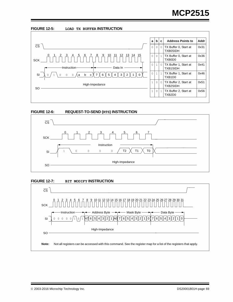
MCP2515
FIGURE 12-5: LOAD TX BUFFER INSTRUCTION
FIGURE 12-6: REQUEST-TO-SEND (RTS) INSTRUCTION
FIGURE 12-7: BIT MODIFY INSTRUCTION
SO
SI
SCK
CS
0 2 3 4 5 6 7 8 9 10 11 12 13 14 151
a c00010 b 7 6 5 4 3 2 1 0
Instruction Data In
High-Impedance
a b c Address Points to Addr
0 0 0 TX Buffer 0, Start at TXB0SIDH
0x31
0 0 1 TX Buffer 0, Start at TXB0D0
0x36
0 1 0 TX Buffer 1, Start at TXB1SIDH
0x41
0 1 1 TX Buffer 1, Start at TXB1D0
0x46
1 0 0 TX Buffer 2, Start at TXB2SIDH
0x51
1 0 1 TX Buffer 2, Start at TXB2D0
0x56
SO
SI
SCK
CS
0 2 3 4 5 6 71
T2 T000001
Instruction
High-Impedance
T1
SO
SI
SCK
CS
0 2 3 4 5 6 7 8 9 10 11 12 13 14 15 16 17 18 19 20 21 221
1 100000 A7 6 5 4 1 A0 7 6 5 4 3 2 1 0
Instruction
High-Impedance
3 20
Address Byte Mask Byte
7 6 5 4 3 2 1 0
23 24 25 26 27 28 29 30 31
Data Byte
Note: Not all registers can be accessed with this command. See the register map for a list of the registers that apply.
2003-2016 Microchip Technology Inc. DS20001801H-page 69
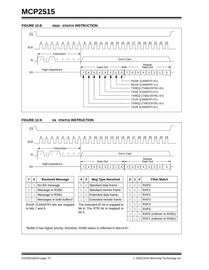
MCP2515
FIGURE 12-8: READ STATUS INSTRUCTION
FIGURE 12-9: RX STATUS INSTRUCTION
SO
SI
SCK
CS
0 2 3 4 5 6 7 8 9 10 11 12 13 14 15 16 17 18 19 20 21 221
0 000101 0
7 6 5 4 3 2 1 0
Instruction
Data OutHigh-Impedance
23
Don’t Care
RX0IF (CANINTF<0>)RX1IF (CANINTF<1>)
TX0IF (CANINTF<2>)
TX1IF (CANINTF<3>)
TX2IF (CANINTF<4>)TXREQ (TXB2CNTRL<3>)
TXREQ (TXB1CNTRL<3>)
TXREQ (TXB0CNTRL<3>)
7 6 5 4 3 2 1 0
Data OutRepeat
SO
SI
SCK
CS
0 2 3 4 5 6 7 8 9 10 11 12 13 14 15 16 17 18 19 20 21 221
0 001101 0
7 6 5 4 3 2 1 0
Instruction
Data OutHigh-Impedance
23
Don’t Care
7 6 5 4 3 2 1 0
Data OutRepeat
2 1 0 Filter Match
0 0 0 RXF0
0 0 1 RXF1
0 1 0 RXF2
0 1 1 RXF3
1 0 0 RXF4
1 0 1 RXF5
1 1 0 RXF0 (rollover to RXB1)
1 1 1 RXF1 (rollover to RXB1)
RXnIF (CANINTF) bits are mappedto bits 7 and 6.
7 6 Received Message
0 0 No RX message
0 1 Message in RXB0
1 0 Message in RXB1
1 1 Messages in both buffers*
The extended ID bit is mapped tobit 4. The RTR bit is mapped tobit 3.
4 3 Msg Type Received
0 0 Standard data frame
0 1 Standard remote frame
1 0 Extended data frame
1 1 Extended remote frame
*Buffer 0 has higher priority; therefore, RXB0 status is reflected in bits<4:0>.
DS20001801H-page 70 2003-2016 Microchip Technology Inc.
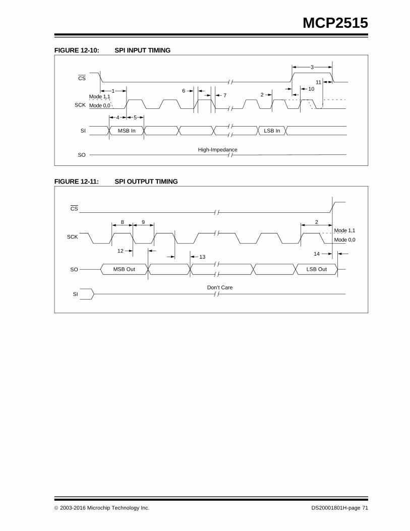
MCP2515
FIGURE 12-10: SPI INPUT TIMING
FIGURE 12-11: SPI OUTPUT TIMING
CS
SCK
SI
SO
1
54
76
3
102
LSB InMSB In
High-Impedance
11
Mode 1,1
Mode 0,0
CS
SCK
SO
8
13
MSB Out LSB Out
2
14
Don’t CareSI
Mode 1,1
Mode 0,0
9
12
2003-2016 Microchip Technology Inc. DS20001801H-page 71

MCP2515
NOTES:
DS20001801H-page 72 2003-2016 Microchip Technology Inc.

MCP2515
13.0 ELECTRICAL CHARACTERISTICS
13.1 Absolute Maximum Ratings†
VDD.............................................................................................................................................................................7.0V
All Inputs and Outputs w.r.t. VSS ........................................................................................................-0.6V to VDD + 1.0V
Storage Temperature .............................................................................................................................. -65°C to +150°C
Ambient Temperature with Power Applied .............................................................................................. -65°C to +125°C
Soldering Temperature of Leads (10 seconds) ..................................................................................................... +300°C
† Notice: Stresses above those listed under “Maximum Ratings” may cause permanent damage to the device. This is a stress rating only and functional operation of the device at those or any other conditions above those indicated in the operational listings of this specification is not implied. Exposure to maximum rating conditions for extended periods may affect device reliability.
2003-2016 Microchip Technology Inc. DS20001801H-page 73

MCP2515
TABLE 13-1: DC CHARACTERISTICS
DC Characteristics VDD = 2.7V to 5.5VIndustrial (I): TAMB = -40°C to +85°CExtended (E): TAMB = -40°C to +125°C
Param.No.
Sym Characteristic Min Max Units Conditions
VDD Supply Voltage 2.7 5.5 V
VRET Register Retention Voltage 2.4 — V
High-Level Input Voltage
VIH RXCAN Pin 2 VDD + 1 V
SCK, CS, SI, TXnRTS Pins 0.7 VDD VDD + 1 V
OSC1 Pin 0.85 VDD VDD V
RESET Pin 0.85 VDD VDD V
Low-Level Input Voltage
VIL RXCAN, TXnRTS Pins -0.3 .15 VDD V
SCK, CS, SI Pins -0.3 0.4 VDD V
OSC1 Pin VSS .3 VDD V
RESET Pin VSS .15 VDD V
Low-Level Output Voltage
VOL TXCAN Pin — 0.6 V IOL = +6.0 mA, VDD = 4.5V
RXnBF Pin — 0.6 V IOL = +8.5 mA, VDD = 4.5V
SO, CLKOUT Pins — 0.6 V IOL = +2.1 mA, VDD = 4.5V
INT Pin — 0.6 V IOL = +1.6 mA, VDD = 4.5V
High-Level Output Voltage V
VOH TXCAN, RXnBF Pins VDD – 0.7 — V IOH = -3.0 mA, VDD = 4.5V
SO, CLKOUT Pins VDD – 0.5 — V IOH = -400 µA, VDD = 4.5V
INT Pin VDD – 0.7 — V IOH = -1.0 mA, VDD = 4.5V
Input Leakage Current
ILI All I/Os except OSC1 and TXnRTS Pins
-1 +1 µA CS = RESET = VDD, VIN = VSS to VDD
OSC1 Pin -5 +5 µA
CINT Internal Capacitance(all inputs and outputs)
— 7 pF TAMB = +25°C, fC = 1.0 MHz,VDD = 0V (Note 1)
IDD Operating Current — 10 mA VDD = 5.5V, FOSC = 25 MHz,FCLK = 1 MHz, SO = Open
IDDS Standby Current (Sleep mode)
— 5 µA CS, TXnRTS = VDD, inputs tied to VDD or VSS, -40°C TO +85°C
— 8 µA CS, TXnRTS = VDD, inputs tied to VDD or VSS, -40°C TO +125°C
Note 1: This parameter is periodically sampled and not 100% tested.
DS20001801H-page 74 2003-2016 Microchip Technology Inc.

MCP2515
TABLE 13-2: OSCILLATOR TIMING CHARACTERISTICS
TABLE 13-3: CAN INTERFACE AC CHARACTERISTICS
TABLE 13-4: RESET AC CHARACTERISTICS
Oscillator Timing Characteristics(1) VDD = 2.7V to 5.5VIndustrial (I): TAMB = -40°C to +85°CExtended (E): TAMB = -40°C to +125°C
Param.No.
Sym Characteristic Min Max Units Conditions
FOSC Clock In Frequency 11
4025
MHzMHz
VDD = 4.5V to 5.5VVDD = 2.7V to 5.5V
TOSC Clock In Period 2540
10001000
nsns
VDD = 4.5V to 5.5VVDD = 2.7V to 5.5V
TDUTY Duty Cycle(external clock input)
0.45 0.55 — TOSH/(TOSH + TOSL)
Note 1: This parameter is periodically sampled and not 100% tested.
CAN Interface AC Characteristics VDD = 2.7V to 5.5VIndustrial (I): TAMB = -40°C to +85°CExtended (E): TAMB = -40°C to +125°C
Param.No.
Sym Characteristic Min Max Units Conditions
TWF Wake-up Noise Filter 100 — ns
Reset AC Characteristics VDD = 2.7V to 5.5VIndustrial (I): TAMB = -40°C to +85°CExtended (E): TAMB = -40°C to +125°C
Param.No.
Sym Characteristic Min Max Units Conditions
tRL RESET Pin Low Time 2 — µs
2003-2016 Microchip Technology Inc. DS20001801H-page 75

MCP2515
TABLE 13-5: CLKOUT PIN AC CHARACTERISTICS
FIGURE 13-1: START-OF-FRAME PIN AC CHARACTERISTICS
CLKOUT Pin AC/DC Characteristics VDD = 2.7V to 5.5VIndustrial (I): TAMB = -40°C to +85°CExtended (E): TAMB = -40°C to +125°C
Param.No.
Sym Characteristic Min Max Units Conditions
thCLKOUT CLKOUT Pin High Time 15 — ns TOSC = 40 ns (Note 1)
tlCLKOUT CLKOUT Pin Low Time 15 — ns TOSC = 40 ns (Note 1)
trCLKOUT CLKOUT Pin Rise Time — 5 ns Measured from 0.3 VDD to 0.7 VDD (Note 1)
tfCLKOUT CLKOUT Pin Fall Time — 5 ns Measured from 0.7 VDD to 0.3 VDD (Note 1)
tdCLKOUT CLKOUT Propagation Delay — 100 ns (Note 1)
15 thSOF Start-of-Frame High Time — 2 TOSC ns (Note 1)
16 tdSOF Start-of-Frame Propagation Delay
— 2 TOSC + 0.5 TQ ns Measured from CAN bit sample point; device is a receiver, BRP<5:0> (CNF1<5:0>) = 0 (Note 2)
Note 1: All CLKOUT mode functionality and output frequency are tested at device frequency limits; however, the CLKOUT prescaler is set to divide by one. This parameter is periodically sampled and not 100% tested.
2: Design guidance only, not tested.
RXCAN16
15
Sample Point
DS20001801H-page 76 2003-2016 Microchip Technology Inc.
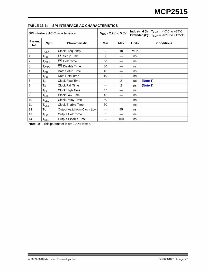
MCP2515
TABLE 13-6: SPI INTERFACE AC CHARACTERISTICS
SPI Interface AC Characteristics VDD = 2.7V to 5.5VIndustrial (I): TAMB = -40°C to +85°CExtended (E): TAMB = -40°C to +125°C
Param.No.
Sym Characteristic Min Max Units Conditions
FCLK Clock Frequency — 10 MHz
1 TCSS CS Setup Time 50 — ns
2 TCSH CS Hold Time 50 — ns
3 TCSD CS Disable Time 50 — ns
4 TSU Data Setup Time 10 — ns
5 THD Data Hold Time 10 — ns
6 TR Clock Rise Time — 2 µs (Note 1)
7 TF Clock Fall Time — 2 µs (Note 1)
8 THI Clock High Time 45 — ns
9 TLO Clock Low Time 45 — ns
10 TCLD Clock Delay Time 50 — ns
11 TCLE Clock Enable Time 50 — ns
12 TV Output Valid from Clock Low — 45 ns
13 THO Output Hold Time 0 — ns
14 TDIS Output Disable Time — 100 ns
Note 1: This parameter is not 100% tested.
2003-2016 Microchip Technology Inc. DS20001801H-page 77

MCP2515
NOTES:
DS20001801H-page 78 2003-2016 Microchip Technology Inc.

MCP2515
14.0 PACKAGING INFORMATION
14.1 Package Marking Information
18-Lead PDIP (300 mil)
18-Lead SOIC (7.50 mm)
20-Lead TSSOP (4.4 mm)
XXXXXXXXXXXXXNNN
YYWW
XXXXXXXXXXXXXXXXXXXXXXXXXXXXXXXXXXXX
YYWWNNN
XXXXXXXXXXXXXXXXXXXXXXXXXXXXXXXXXX
YYWWNNN
Example:
Example:
Example:
MCP2515-E/
1634256
MCP2515-I/P^^
1634256
Legend: XX...X Customer-specific informationY Year code (last digit of calendar year)YY Year code (last 2 digits of calendar year)WW Week code (week of January 1 is week ‘01’)NNN Alphanumeric traceability code Pb-free JEDEC designator for Matte Tin (Sn)* This package is Pb-free. The Pb-free JEDEC designator ( )
can be found on the outer packaging for this package.
Note: In the event the full Microchip part number cannot be marked on one line, it willbe carried over to the next line, thus limiting the number of availablecharacters for customer-specific information.
3e
3e
SO^^
3e
3e
3e
XXXXX
20-Lead QFN (4x4x0.9 mm)
YWWNNN
Example:
XXXXXX 3e
MCP2515-I/ST 256
1634
XXXXXXMCP
634256E/ML2515-
2003-2016 Microchip Technology Inc. DS20001801H-page 79

MCP2515
���������� ������������������������������
�
�� �� �� ������ �!"�����#�$�%��&"��'��� ��(�)"&�'"!&�)�����&�#�*�&����&�����&���#������� +������%����&�,����&��!&���-� ��'��!��!�����#�.��#��&�����"#��'�#�%��!����&"!��!����#�%��!����&"!��!�!������&��$���#�����/����!�#���� ��'��!��������#�&���������������.�0������
1�,2 1�!�����'��!���� ���&��������$��&� ��"��!�*��*�&�"&�&������!�
�� � 3�&���'!&��"��&����4����#�*���!(�����!��!���&��������������4�����������%���&������&�#��&��&&�255***�'��������'5���4�����
6��&! �7,8.���'��!���9�'�&! ��7 7:� ��;
7"')��%����! 7 �<��&�� � �����1�, ��&����&��������� � = = ������#�#����4���� ���4��!! �� ���� ��-� ����1�!��&����&��������� �� ���� = =��"�#��&���"�#��>�#&� . �-�� �-�� �-����#�#����4����>�#&� .� ���� ���� ��<�: �����9���&� � �<<� ���� ���� ���&����&��������� 9 ���� ��-� ����9��#� ���4��!! � ���< ���� ����6����9��#�>�#&� )� ���� ��?� ����9*��9��#�>�#&� ) ���� ���< ����: ������*����������+ �1 = = ��-�
NOTE 1
N
E1
D
1 2 3
A
A1
A2
L
E
eB
c
e
b1
b
������� ������� ��*��� ,������1
DS20001801H-page 80 2003-2016 Microchip Technology Inc.
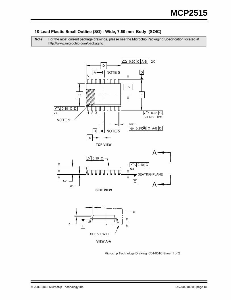
MCP2515
Note: For the most current package drawings, please see the Microchip Packaging Specification located at
http://www.microchip.com/packaging
2003-2016 Microchip Technology Inc. DS20001801H-page 81
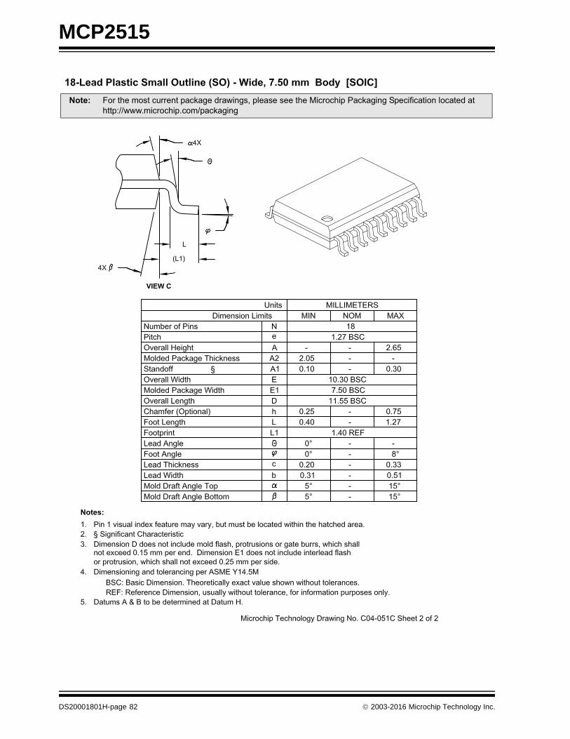
MCP2515
Note: For the most current package drawings, please see the Microchip Packaging Specification located at
http://www.microchip.com/packaging
DS20001801H-page 82 2003-2016 Microchip Technology Inc.

MCP2515
Note: For the most current package drawings, please see the Microchip Packaging Specification located at
http://www.microchip.com/packaging
2003-2016 Microchip Technology Inc. DS20001801H-page 83
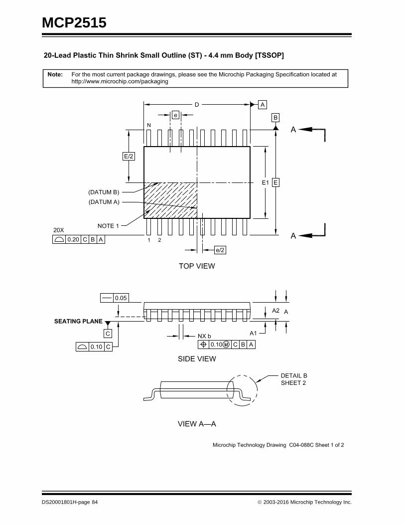
MCP2515
DS20001801H-page 84 2003-2016 Microchip Technology Inc.

MCP2515
2003-2016 Microchip Technology Inc. DS20001801H-page 85
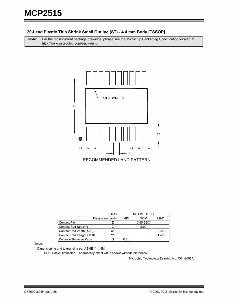
MCP2515
Note: For the most current package drawings, please see the Microchip Packaging Specification located at
http://www.microchip.com/packaging
DS20001801H-page 86 2003-2016 Microchip Technology Inc.
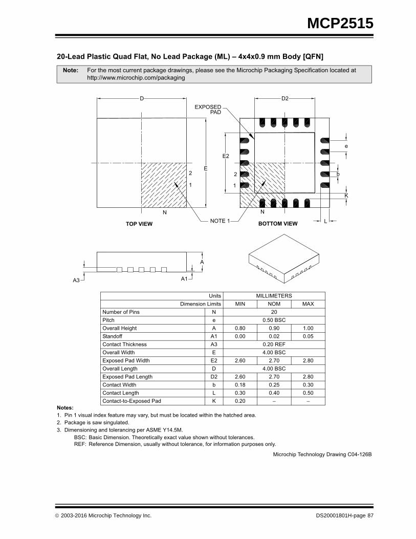
MCP2515
!��������� ��"���#�� $��������%�&��'���()()�*+�������"#��
�
�� �� �� ������ �!"�����#�$�%��&"��'��� ��(�)"&�'"!&�)�����&�#�*�&����&�����&���#������� ���4�����!�!�*�!���"��&�#�-� ��'��!��������#�&���������������.�0������
1�,2 1�!�����'��!���� ���&��������$��&� ��"��!�*��*�&�"&�&������!��.32 ��%��������'��!��(�"!"�����*�&�"&�&������(�%���%'�&����"�!�!�����
�� � 3�&���'!&��"��&����4����#�*���!(�����!��!���&��������������4�����������%���&������&�#��&��&&�255***�'��������'5���4�����
6��&! ��99��. .����'��!���9�'�&! ��7 7:� ��;
7"')��%����! 7 ����&�� � �����1�,: �����8����& � ��<� ���� �����&��#%%� �� ���� ���� ����,�&��&� ���4��!! �- ������.3: �����>�#&� . �����1�,.$�!�#���#�>�#&� .� ��?� ���� ��<�: �����9���&� � �����1�,.$�!�#���#�9���&� �� ��?� ���� ��<�,�&��&�>�#&� ) ���< ���� ��-�,�&��&�9���&� 9 ��-� ���� ����,�&��&�&�.$�!�#���# @ ���� = =
D
EXPOSEDPAD
E
E2
2
1
N
TOP VIEW NOTE 1
N
L
K
b
e
D2
2
1
A
A1A3
BOTTOM VIEW
������� ������� ��*��� ,�����?1
2003-2016 Microchip Technology Inc. DS20001801H-page 87

MCP2515
�� � 3�&���'!&��"��&����4����#�*���!(�����!��!���&��������������4�����������%���&������&�#��&��&&�255***�'��������'5���4�����
DS20001801H-page 88 2003-2016 Microchip Technology Inc.

MCP2515
APPENDIX A: REVISION HISTORY
Revision H (November 2016)
The following is the list of modifications:
1. Updated the voltage range, which was widenedto 2.7V to 5.5V for the E temperature device.There are two parameters that differ betweenthe I and E temperature devices: IDDS and FOSC(TOSC).
2. Specified that the usage of the RXM<1:0> bit set-tings, ‘01’ and ‘10’ in the RXBnCTRL registers isnot recommended.
Revision G (August 2012)
The following is the list of modifications:
1. Updated content in Register 4-1, Register 4-12,Register 4-13, Register 4-16, Register 4-17.
Revision F (October 2010)
The following is the list of modifications:
1. Added 20-lead QFN package (4x4) and relatedinformation.
2. Updated Table 1-1.
3. Updated the Product Identification Systemsection.
Revision E (November 2007)
• Removed preliminary watermark.
• Updated templates.
• Updated register information.
• Updated package outline drawings.
Revision D (April 2005)
• Added Table 8-1 and Table 8-2 in Section 8.0 “Oscillator”. Added note box following tables.
• Changed address bits in column heading in Table 11-1, Section 11.0 “Register Map”.
• Modified Section 14.0 “Packaging Information” to reflect pb free device markings.
• Appendix A Revision History: Rearranged order of importance.
Revision C (November 2004)
• Section 9.0 “Reset” added.
• Heading 12.1: added notebox.Heading 12.6: Changed verbiage within paragraph in Section 12.0 “SPI Interface”.
• Added Appendix A: Revision History.
Revision B (September 2003)
• Front page bullet: Standby current (typical) (Sleep mode) changed from 10 µA to 1 µA.
• Added notebox for maximum frequency on CLKOUT in Section 8.2 “CLKOUT Pin”.
• Section 12.0 “SPI Interface”, Table 12-1:
- Changed supply voltage minimum to 2.7V.
- Internal Capacitance: Changed VDD condition to 0V.
- Standby Current (Sleep mode): Split specification into -40°C to +85°C and-40°C to +125°C.
Revision A (May 2003)
• Original Release of this Document.
2003-2016 Microchip Technology Inc. DS20001801H-page 89

MCP2515
NOTES:
DS20001801H-page 90 2003-2016 Microchip Technology Inc.
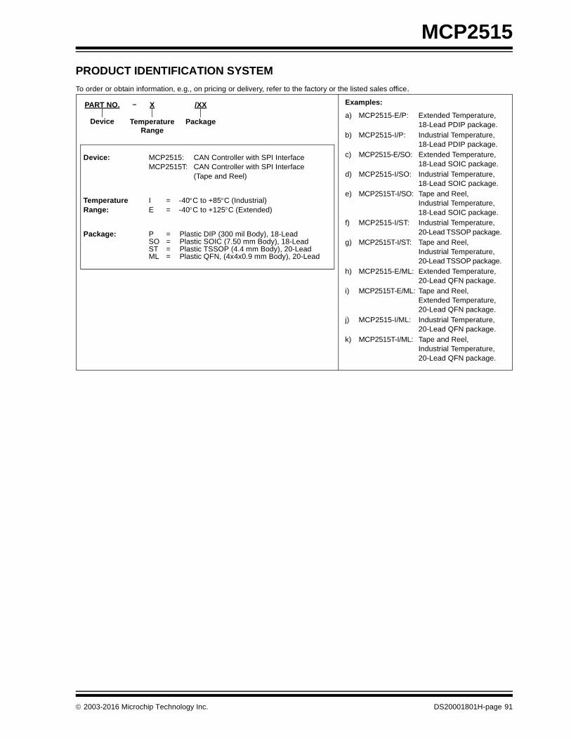
MCP2515
PRODUCT IDENTIFICATION SYSTEM
To order or obtain information, e.g., on pricing or delivery, refer to the factory or the listed sales office.
Device: MCP2515: CAN Controller with SPI InterfaceMCP2515T: CAN Controller with SPI Interface
(Tape and Reel)
Temperature Range:
I = -40C to +85C (Industrial)E = -40C to +125C (Extended)
Package: P = Plastic DIP (300 mil Body), 18-LeadSO = Plastic SOIC (7.50 mm Body), 18-LeadST = Plastic TSSOP (4.4 mm Body), 20-LeadML = Plastic QFN, (4x4x0.9 mm Body), 20-Lead
PART NO. X /XX
PackageTemperatureRange
Device
Examples:
a) MCP2515-E/P: Extended Temperature, 18-Lead PDIP package.
b) MCP2515-I/P: Industrial Temperature, 18-Lead PDIP package.
c) MCP2515-E/SO: Extended Temperature, 18-Lead SOIC package.
d) MCP2515-I/SO: Industrial Temperature,18-Lead SOIC package.
e) MCP2515T-I/SO: Tape and Reel,Industrial Temperature,18-Lead SOIC package.
f) MCP2515-I/ST: Industrial Temperature,20-Lead TSSOP package.
g) MCP2515T-I/ST: Tape and Reel,Industrial Temperature,20-Lead TSSOP package.
h) MCP2515-E/ML: Extended Temperature,20-Lead QFN package.
i) MCP2515T-E/ML: Tape and Reel,Extended Temperature,20-Lead QFN package.
j) MCP2515-I/ML: Industrial Temperature,20-Lead QFN package.
k) MCP2515T-I/ML: Tape and Reel,Industrial Temperature,20-Lead QFN package.
–
2003-2016 Microchip Technology Inc. DS20001801H-page 91

MCP2515
NOTES:
DS20001801H-page 92 2003-2016 Microchip Technology Inc.
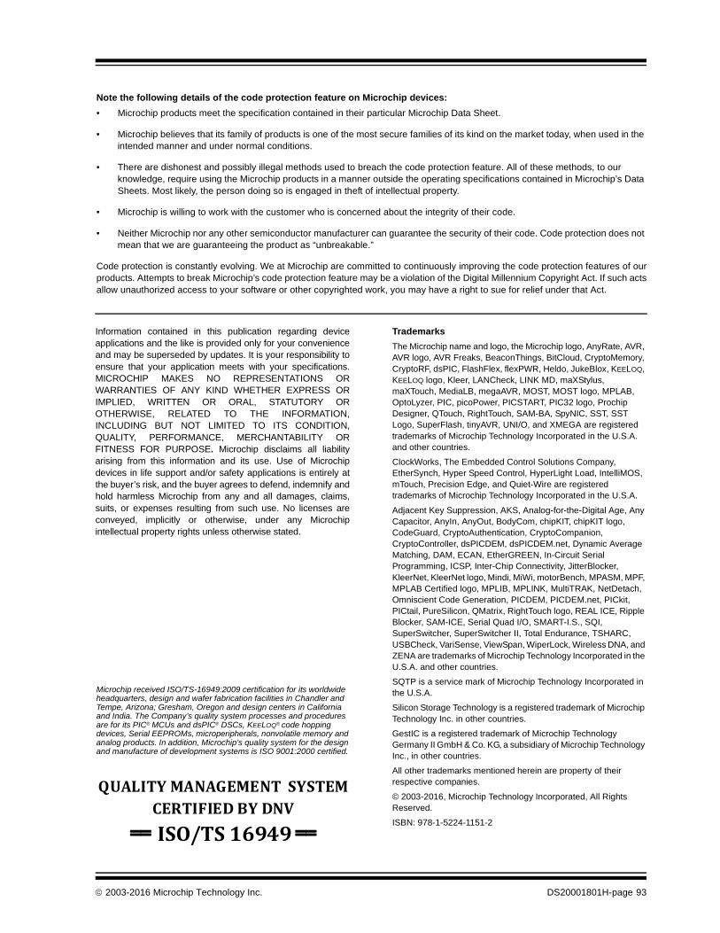
Note the following details of the code protection feature on Microchip devices:
• Microchip products meet the specification contained in their particular Microchip Data Sheet.
• Microchip believes that its family of products is one of the most secure families of its kind on the market today, when used in the intended manner and under normal conditions.
• There are dishonest and possibly illegal methods used to breach the code protection feature. All of these methods, to our knowledge, require using the Microchip products in a manner outside the operating specifications contained in Microchip’s Data Sheets. Most likely, the person doing so is engaged in theft of intellectual property.
• Microchip is willing to work with the customer who is concerned about the integrity of their code.
• Neither Microchip nor any other semiconductor manufacturer can guarantee the security of their code. Code protection does not mean that we are guaranteeing the product as “unbreakable.”
Code protection is constantly evolving. We at Microchip are committed to continuously improving the code protection features of ourproducts. Attempts to break Microchip’s code protection feature may be a violation of the Digital Millennium Copyright Act. If such actsallow unauthorized access to your software or other copyrighted work, you may have a right to sue for relief under that Act.
Information contained in this publication regarding deviceapplications and the like is provided only for your convenienceand may be superseded by updates. It is your responsibility toensure that your application meets with your specifications.MICROCHIP MAKES NO REPRESENTATIONS ORWARRANTIES OF ANY KIND WHETHER EXPRESS ORIMPLIED, WRITTEN OR ORAL, STATUTORY OROTHERWISE, RELATED TO THE INFORMATION,INCLUDING BUT NOT LIMITED TO ITS CONDITION,QUALITY, PERFORMANCE, MERCHANTABILITY ORFITNESS FOR PURPOSE. Microchip disclaims all liabilityarising from this information and its use. Use of Microchipdevices in life support and/or safety applications is entirely atthe buyer’s risk, and the buyer agrees to defend, indemnify andhold harmless Microchip from any and all damages, claims,suits, or expenses resulting from such use. No licenses areconveyed, implicitly or otherwise, under any Microchipintellectual property rights unless otherwise stated.
2003-2016 Microchip Technology Inc.
Microchip received ISO/TS-16949:2009 certification for its worldwide headquarters, design and wafer fabrication facilities in Chandler and Tempe, Arizona; Gresham, Oregon and design centers in California and India. The Company’s quality system processes and procedures are for its PIC® MCUs and dsPIC® DSCs, KEELOQ® code hopping devices, Serial EEPROMs, microperipherals, nonvolatile memory and analog products. In addition, Microchip’s quality system for the design and manufacture of development systems is ISO 9001:2000 certified.
QUALITY MANAGEMENT SYSTEM CERTIFIED BY DNV
== ISO/TS 16949 ==
Trademarks
The Microchip name and logo, the Microchip logo, AnyRate, AVR, AVR logo, AVR Freaks, BeaconThings, BitCloud, CryptoMemory, CryptoRF, dsPIC, FlashFlex, flexPWR, Heldo, JukeBlox, KEELOQ, KEELOQ logo, Kleer, LANCheck, LINK MD, maXStylus, maXTouch, MediaLB, megaAVR, MOST, MOST logo, MPLAB, OptoLyzer, PIC, picoPower, PICSTART, PIC32 logo, Prochip Designer, QTouch, RightTouch, SAM-BA, SpyNIC, SST, SST Logo, SuperFlash, tinyAVR, UNI/O, and XMEGA are registered trademarks of Microchip Technology Incorporated in the U.S.A. and other countries.
ClockWorks, The Embedded Control Solutions Company, EtherSynch, Hyper Speed Control, HyperLight Load, IntelliMOS, mTouch, Precision Edge, and Quiet-Wire are registered trademarks of Microchip Technology Incorporated in the U.S.A.
Adjacent Key Suppression, AKS, Analog-for-the-Digital Age, Any Capacitor, AnyIn, AnyOut, BodyCom, chipKIT, chipKIT logo, CodeGuard, CryptoAuthentication, CryptoCompanion, CryptoController, dsPICDEM, dsPICDEM.net, Dynamic Average Matching, DAM, ECAN, EtherGREEN, In-Circuit Serial Programming, ICSP, Inter-Chip Connectivity, JitterBlocker, KleerNet, KleerNet logo, Mindi, MiWi, motorBench, MPASM, MPF, MPLAB Certified logo, MPLIB, MPLINK, MultiTRAK, NetDetach, Omniscient Code Generation, PICDEM, PICDEM.net, PICkit, PICtail, PureSilicon, QMatrix, RightTouch logo, REAL ICE, Ripple Blocker, SAM-ICE, Serial Quad I/O, SMART-I.S., SQI, SuperSwitcher, SuperSwitcher II, Total Endurance, TSHARC, USBCheck, VariSense, ViewSpan, WiperLock, Wireless DNA, and ZENA are trademarks of Microchip Technology Incorporated in the U.S.A. and other countries.
SQTP is a service mark of Microchip Technology Incorporated in the U.S.A.
Silicon Storage Technology is a registered trademark of Microchip Technology Inc. in other countries.
GestIC is a registered trademark of Microchip Technology Germany II GmbH & Co. KG, a subsidiary of Microchip Technology Inc., in other countries.
All other trademarks mentioned herein are property of their respective companies.
© 2003-2016, Microchip Technology Incorporated, All Rights Reserved.
ISBN: 978-1-5224-1151-2
DS20001801H-page 93

DS20001801H-page 94 2003-2016 Microchip Technology Inc.
AMERICASCorporate Office2355 West Chandler Blvd.Chandler, AZ 85224-6199Tel: 480-792-7200 Fax: 480-792-7277Technical Support: http://www.microchip.com/supportWeb Address: www.microchip.com
AtlantaDuluth, GA Tel: 678-957-9614 Fax: 678-957-1455
Austin, TXTel: 512-257-3370
BostonWestborough, MA Tel: 774-760-0087 Fax: 774-760-0088
ChicagoItasca, IL Tel: 630-285-0071 Fax: 630-285-0075
DallasAddison, TX Tel: 972-818-7423 Fax: 972-818-2924
DetroitNovi, MI Tel: 248-848-4000
Houston, TX Tel: 281-894-5983
IndianapolisNoblesville, IN Tel: 317-773-8323Fax: 317-773-5453Tel: 317-536-2380
Los AngelesMission Viejo, CA Tel: 949-462-9523Fax: 949-462-9608Tel: 951-273-7800
Raleigh, NC Tel: 919-844-7510
New York, NY Tel: 631-435-6000
San Jose, CA Tel: 408-735-9110Tel: 408-436-4270
Canada - TorontoTel: 905-695-1980 Fax: 905-695-2078
ASIA/PACIFICAsia Pacific OfficeSuites 3707-14, 37th FloorTower 6, The GatewayHarbour City, Kowloon
Hong KongTel: 852-2943-5100Fax: 852-2401-3431
Australia - SydneyTel: 61-2-9868-6733Fax: 61-2-9868-6755
China - BeijingTel: 86-10-8569-7000 Fax: 86-10-8528-2104
China - ChengduTel: 86-28-8665-5511Fax: 86-28-8665-7889
China - ChongqingTel: 86-23-8980-9588Fax: 86-23-8980-9500
China - DongguanTel: 86-769-8702-9880
China - GuangzhouTel: 86-20-8755-8029
China - HangzhouTel: 86-571-8792-8115 Fax: 86-571-8792-8116
China - Hong Kong SARTel: 852-2943-5100 Fax: 852-2401-3431
China - NanjingTel: 86-25-8473-2460Fax: 86-25-8473-2470
China - QingdaoTel: 86-532-8502-7355Fax: 86-532-8502-7205
China - ShanghaiTel: 86-21-3326-8000 Fax: 86-21-3326-8021
China - ShenyangTel: 86-24-2334-2829Fax: 86-24-2334-2393
China - ShenzhenTel: 86-755-8864-2200 Fax: 86-755-8203-1760
China - WuhanTel: 86-27-5980-5300Fax: 86-27-5980-5118
China - XianTel: 86-29-8833-7252Fax: 86-29-8833-7256
ASIA/PACIFICChina - XiamenTel: 86-592-2388138 Fax: 86-592-2388130
China - ZhuhaiTel: 86-756-3210040 Fax: 86-756-3210049
India - BangaloreTel: 91-80-3090-4444 Fax: 91-80-3090-4123
India - New DelhiTel: 91-11-4160-8631Fax: 91-11-4160-8632
India - PuneTel: 91-20-3019-1500
Japan - OsakaTel: 81-6-6152-7160 Fax: 81-6-6152-9310
Japan - TokyoTel: 81-3-6880- 3770 Fax: 81-3-6880-3771
Korea - DaeguTel: 82-53-744-4301Fax: 82-53-744-4302
Korea - SeoulTel: 82-2-554-7200Fax: 82-2-558-5932 or 82-2-558-5934
Malaysia - Kuala LumpurTel: 60-3-6201-9857Fax: 60-3-6201-9859
Malaysia - PenangTel: 60-4-227-8870Fax: 60-4-227-4068
Philippines - ManilaTel: 63-2-634-9065Fax: 63-2-634-9069
SingaporeTel: 65-6334-8870Fax: 65-6334-8850
Taiwan - Hsin ChuTel: 886-3-5778-366Fax: 886-3-5770-955
Taiwan - KaohsiungTel: 886-7-213-7830
Taiwan - TaipeiTel: 886-2-2508-8600 Fax: 886-2-2508-0102
Thailand - BangkokTel: 66-2-694-1351Fax: 66-2-694-1350
EUROPEAustria - WelsTel: 43-7242-2244-39Fax: 43-7242-2244-393
Denmark - CopenhagenTel: 45-4450-2828 Fax: 45-4485-2829
Finland - EspooTel: 358-9-4520-820
France - ParisTel: 33-1-69-53-63-20 Fax: 33-1-69-30-90-79
France - Saint CloudTel: 33-1-30-60-70-00
Germany - GarchingTel: 49-8931-9700Germany - HaanTel: 49-2129-3766400
Germany - HeilbronnTel: 49-7131-67-3636
Germany - KarlsruheTel: 49-721-625370
Germany - MunichTel: 49-89-627-144-0 Fax: 49-89-627-144-44
Germany - RosenheimTel: 49-8031-354-560
Israel - Ra’anana Tel: 972-9-744-7705
Italy - Milan Tel: 39-0331-742611 Fax: 39-0331-466781
Italy - PadovaTel: 39-049-7625286
Netherlands - DrunenTel: 31-416-690399 Fax: 31-416-690340
Norway - TrondheimTel: 47-7289-7561
Poland - WarsawTel: 48-22-3325737
Romania - BucharestTel: 40-21-407-87-50
Spain - MadridTel: 34-91-708-08-90Fax: 34-91-708-08-91
Sweden - GothenbergTel: 46-31-704-60-40
Sweden - StockholmTel: 46-8-5090-4654
UK - WokinghamTel: 44-118-921-5800Fax: 44-118-921-5820
Worldwide Sales and Service
11/07/16
Related Documents