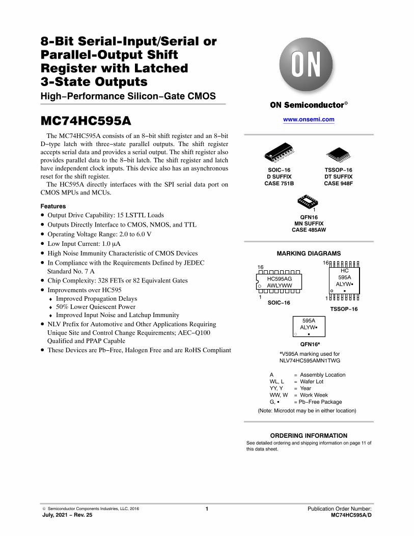
© Semiconductor Components Industries, LLC, 2016 July, 2021 − Rev. 25 1 Publication Order Number: MC74HC595A/D 8-Bit Serial-Input/Serial or Parallel-Output Shift Register with Latched 3-State Outputs High−Performance Silicon−Gate CMOS MC74HC595A The MC74HC595A consists of an 8−bit shift register and an 8−bit D−type latch with three−state parallel outputs. The shift register accepts serial data and provides a serial output. The shift register also provides parallel data to the 8−bit latch. The shift register and latch have independent clock inputs. This device also has an asynchronous reset for the shift register. The HC595A directly interfaces with the SPI serial data port on CMOS MPUs and MCUs. Features • Output Drive Capability: 15 LSTTL Loads • Outputs Directly Interface to CMOS, NMOS, and TTL • Operating Voltage Range: 2.0 to 6.0 V • Low Input Current: 1.0 mA • High Noise Immunity Characteristic of CMOS Devices • In Compliance with the Requirements Defined by JEDEC Standard No. 7 A • Chip Complexity: 328 FETs or 82 Equivalent Gates • Improvements over HC595 ♦ Improved Propagation Delays ♦ 50% Lower Quiescent Power ♦ Improved Input Noise and Latchup Immunity • NLV Prefix for Automotive and Other Applications Requiring Unique Site and Control Change Requirements; AEC−Q100 Qualified and PPAP Capable • These Devices are Pb−Free, Halogen Free and are RoHS Compliant www. onsemi.com MARKING DIAGRAMS A = Assembly Location WL, L = Wafer Lot YY, Y = Year WW, W = Work Week G, G = Pb−Free Package See detailed ordering and shipping information on page 11 of this data sheet. ORDERING INFORMATION SOIC−16 TSSOP−16 1 16 HC595AG AWLYWW HC 595A ALYWG G 1 16 (Note: Microdot may be in either location) SOIC−16 D SUFFIX CASE 751B TSSOP−16 DT SUFFIX CASE 948F QFN16 MN SUFFIX CASE 485AW 1 595A ALYWG G QFN16* *V595A marking used for NLV74HC595AMN1TWG

Welcome message from author
This document is posted to help you gain knowledge. Please leave a comment to let me know what you think about it! Share it to your friends and learn new things together.
Transcript
© Semiconductor Components Industries, LLC, 2016
July, 2021 − Rev. 251 Publication Order Number:
MC74HC595A/D
8-Bit Serial-Input/Serial orParallel-Output ShiftRegister with Latched3-State OutputsHigh−Performance Silicon−Gate CMOS
MC74HC595AThe MC74HC595A consists of an 8−bit shift register and an 8−bit
D−type latch with three−state parallel outputs. The shift registeraccepts serial data and provides a serial output. The shift register alsoprovides parallel data to the 8−bit latch. The shift register and latchhave independent clock inputs. This device also has an asynchronousreset for the shift register.
The HC595A directly interfaces with the SPI serial data port onCMOS MPUs and MCUs.
Features• Output Drive Capability: 15 LSTTL Loads
• Outputs Directly Interface to CMOS, NMOS, and TTL
• Operating Voltage Range: 2.0 to 6.0 V
• Low Input Current: 1.0 �A
• High Noise Immunity Characteristic of CMOS Devices
• In Compliance with the Requirements Defined by JEDECStandard No. 7 A
• Chip Complexity: 328 FETs or 82 Equivalent Gates
• Improvements over HC595♦ Improved Propagation Delays♦ 50% Lower Quiescent Power♦ Improved Input Noise and Latchup Immunity
• NLV Prefix for Automotive and Other Applications RequiringUnique Site and Control Change Requirements; AEC−Q100Qualified and PPAP Capable
• These Devices are Pb−Free, Halogen Free and are RoHS Compliant
www.onsemi.com
MARKING DIAGRAMS
A = Assembly LocationWL, L = Wafer LotYY, Y = YearWW, W = Work WeekG, � = Pb−Free Package
See detailed ordering and shipping information on page 11 ofthis data sheet.
ORDERING INFORMATION
SOIC−16TSSOP−16
1
16
HC595AGAWLYWW
HC595A
ALYW�
�
1
16
(Note: Microdot may be in either location)
SOIC−16D SUFFIX
CASE 751B
TSSOP−16DT SUFFIXCASE 948F
QFN16MN SUFFIX
CASE 485AW
1
595AALYW�
�
QFN16*
*V595A marking used forNLV74HC595AMN1TWG
MC74HC595A
www.onsemi.com2
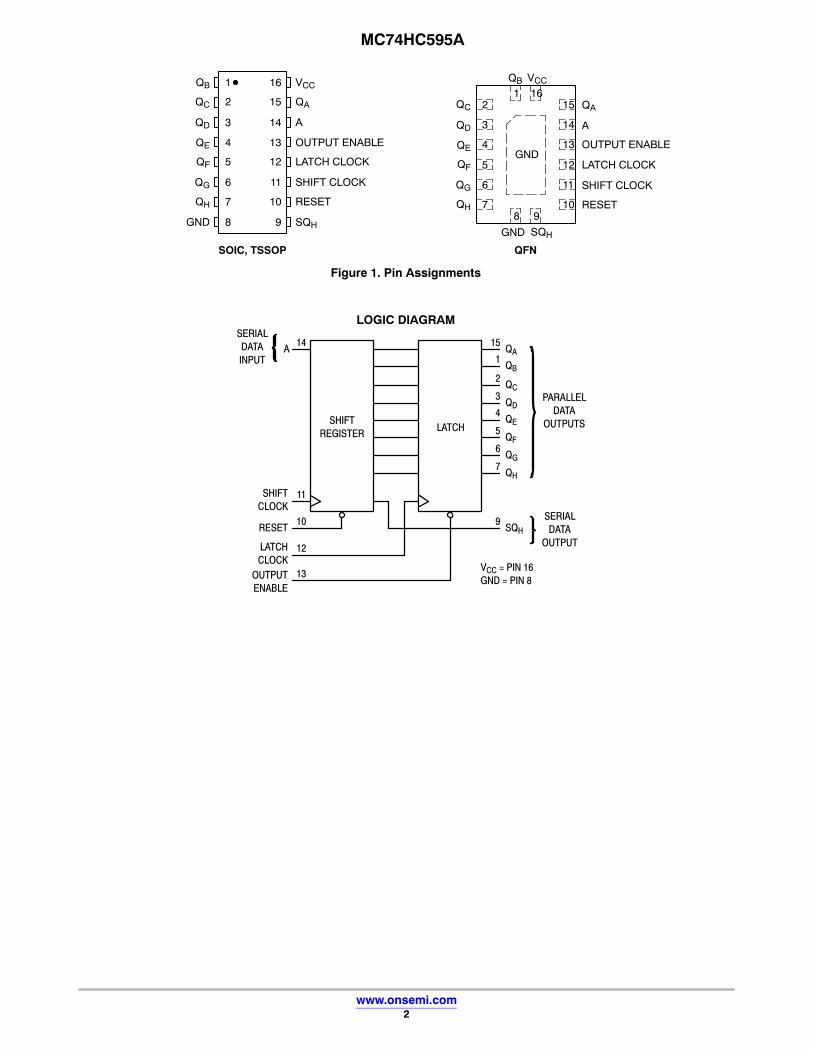
Figure 1. Pin Assignments
1 162 15
3 14
4 13
5 12
6 11
7 108 9
GND
VCC
SQHGND
13
14
15
16
9
10
11
125
4
3
2
1
8
7
6
LATCH CLOCK
OUTPUT ENABLE
A
QA
VCC
SQH
RESET
SHIFT CLOCK
QE
QD
QC
QB
GND
QH
QG
QF
QB
QE
QD
QC
QH
QG
QF LATCH CLOCK
OUTPUT ENABLE
A
QA
RESET
SHIFT CLOCK
SOIC, TSSOP QFN
LOGIC DIAGRAMSERIALDATAINPUT
14
11
10
12
13
SHIFTCLOCK
RESET
LATCHCLOCK
OUTPUTENABLE
SHIFTREGISTER LATCH
15
1
2
3
4
5
6
7
9
QA
QB
QC
QD
QE
QF
QG
QH
SQH
A
VCC = PIN 16GND = PIN 8
PARALLELDATA
OUTPUTS
SERIALDATA
OUTPUT
MC74HC595A
www.onsemi.com3
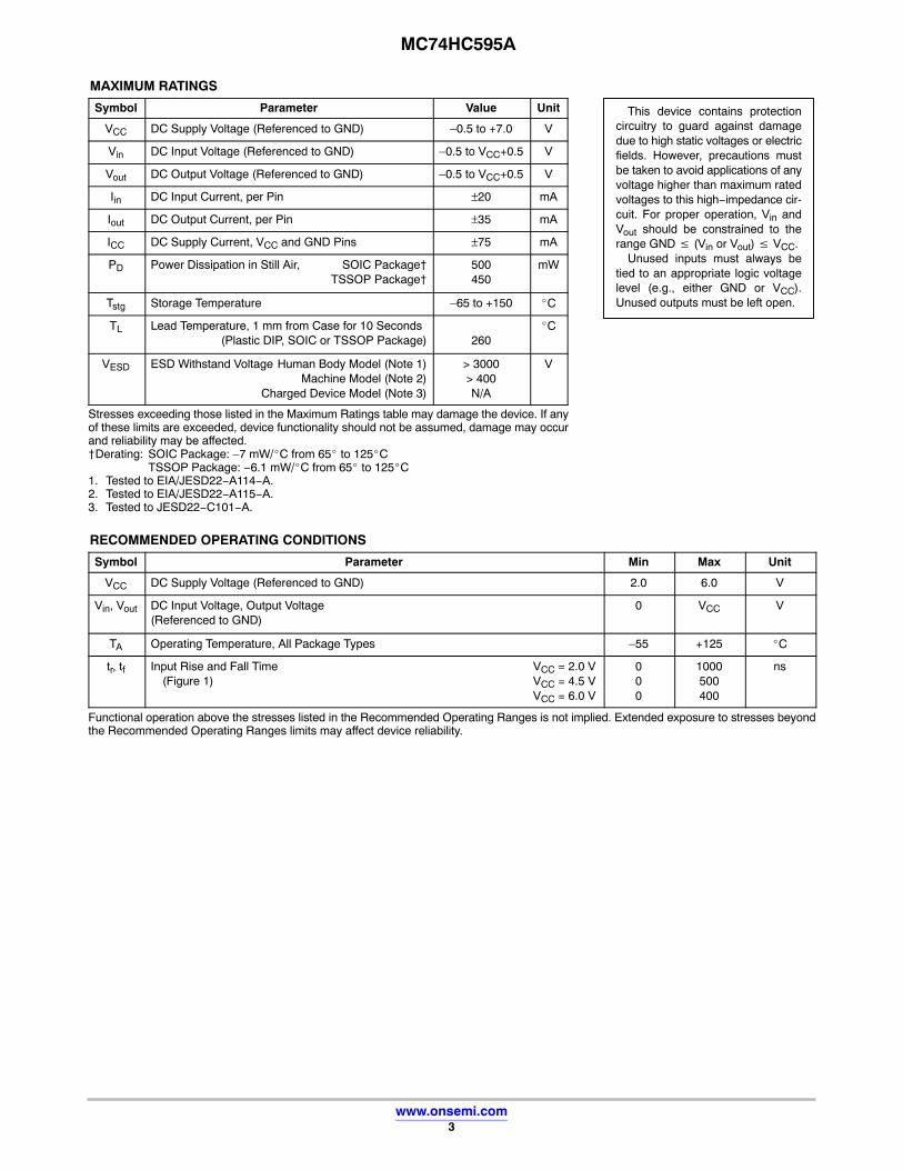
MAXIMUM RATINGS
Symbol Parameter Value Unit
VCC DC Supply Voltage (Referenced to GND) –0.5 to +7.0 V
Vin DC Input Voltage (Referenced to GND) –0.5 to VCC+0.5 V
Vout DC Output Voltage (Referenced to GND) –0.5 to VCC+0.5 V
Iin DC Input Current, per Pin ±20 mA
Iout DC Output Current, per Pin ±35 mA
ICC DC Supply Current, VCC and GND Pins ±75 mA
PD Power Dissipation in Still Air, SOIC Package†TSSOP Package†
500450
mW
Tstg Storage Temperature –65 to +150 �C
TL Lead Temperature, 1 mm from Case for 10 Seconds(Plastic DIP, SOIC or TSSOP Package) 260
�C
VESD ESD Withstand Voltage Human Body Model (Note 1)Machine Model (Note 2)
Charged Device Model (Note 3)
> 3000> 400N/A
V
Stresses exceeding those listed in the Maximum Ratings table may damage the device. If anyof these limits are exceeded, device functionality should not be assumed, damage may occurand reliability may be affected.†Derating: SOIC Package: –7 mW/�C from 65� to 125�C
TSSOP Package: −6.1 mW/�C from 65� to 125�C1. Tested to EIA/JESD22−A114−A.2. Tested to EIA/JESD22−A115−A.3. Tested to JESD22−C101−A.
RECOMMENDED OPERATING CONDITIONS
Symbol Parameter Min Max Unit
VCC DC Supply Voltage (Referenced to GND) 2.0 6.0 V
Vin, Vout DC Input Voltage, Output Voltage(Referenced to GND)
0 VCC V
TA Operating Temperature, All Package Types –55 +125 �C
tr, tf Input Rise and Fall Time VCC = 2.0 V(Figure 1) VCC = 4.5 V
VCC = 6.0 V
000
1000500400
ns
Functional operation above the stresses listed in the Recommended Operating Ranges is not implied. Extended exposure to stresses beyondthe Recommended Operating Ranges limits may affect device reliability.
This device contains protectioncircuitry to guard against damagedue to high static voltages or electricfields. However, precautions mustbe taken to avoid applications of anyvoltage higher than maximum ratedvoltages to this high−impedance cir-cuit. For proper operation, Vin andVout should be constrained to therange GND � (Vin or Vout) � VCC.
Unused inputs must always betied to an appropriate logic voltagelevel (e.g., either GND or VCC).Unused outputs must be left open.
MC74HC595A
www.onsemi.com4
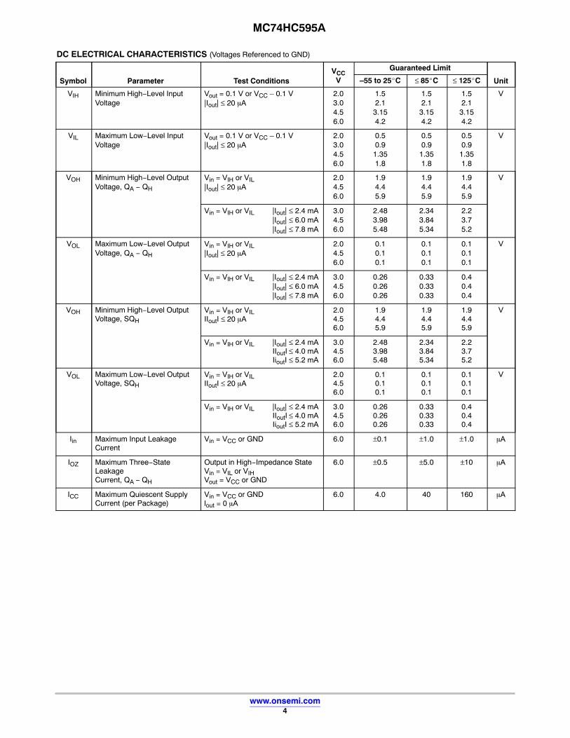
DC ELECTRICAL CHARACTERISTICS (Voltages Referenced to GND)
Symbol Parameter Test ConditionsVCC
V
Guaranteed Limit
Unit–55 to 25�C ≤ 85�C ≤ 125�C
VIH Minimum High−Level InputVoltage
Vout = 0.1 V or VCC – 0.1 V|Iout| ≤ 20 �A
2.03.04.56.0
1.52.13.154.2
1.52.13.154.2
1.52.13.154.2
V
VIL Maximum Low−Level InputVoltage
Vout = 0.1 V or VCC – 0.1 V|Iout| ≤ 20 �A
2.03.04.56.0
0.50.91.351.8
0.50.91.351.8
0.50.91.351.8
V
VOH Minimum High−Level OutputVoltage, QA − QH
Vin = VIH or VIL|Iout| ≤ 20 �A
2.04.56.0
1.94.45.9
1.94.45.9
1.94.45.9
V
Vin = VIH or VIL |Iout| ≤ 2.4 mA|Iout| ≤ 6.0 mA|Iout| ≤ 7.8 mA
3.04.56.0
2.483.985.48
2.343.845.34
2.23.75.2
VOL Maximum Low−Level OutputVoltage, QA − QH
Vin = VIH or VIL|Iout| ≤ 20 �A
2.04.56.0
0.10.10.1
0.10.10.1
0.10.10.1
V
Vin = VIH or VIL |Iout| ≤ 2.4 mA|Iout| ≤ 6.0 mA|Iout| ≤ 7.8 mA
3.04.56.0
0.260.260.26
0.330.330.33
0.40.40.4
VOH Minimum High−Level OutputVoltage, SQH
Vin = VIH or VILIIoutI ≤ 20 �A
2.04.56.0
1.94.45.9
1.94.45.9
1.94.45.9
V
Vin = VIH or VIL |Iout| ≤ 2.4 mAIIoutI ≤ 4.0 mA
IioutI ≤ 5.2 mA
3.04.56.0
2.483.985.48
2.343.845.34
2.23.75.2
VOL Maximum Low−Level OutputVoltage, SQH
Vin = VIH or VILIIoutI ≤ 20 �A
2.04.56.0
0.10.10.1
0.10.10.1
0.10.10.1
V
Vin = VIH or VIL |Iout| ≤ 2.4 mAIIoutI ≤ 4.0 mA
IioutI ≤ 5.2 mA
3.04.56.0
0.260.260.26
0.330.330.33
0.40.40.4
Iin Maximum Input LeakageCurrent
Vin = VCC or GND 6.0 ±0.1 ±1.0 ±1.0 �A
IOZ Maximum Three−StateLeakageCurrent, QA − QH
Output in High−Impedance StateVin = VIL or VIHVout = VCC or GND
6.0 ±0.5 ±5.0 ±10 �A
ICC Maximum Quiescent SupplyCurrent (per Package)
Vin = VCC or GNDlout = 0 �A
6.0 4.0 40 160 �A
MC74HC595A
www.onsemi.com5
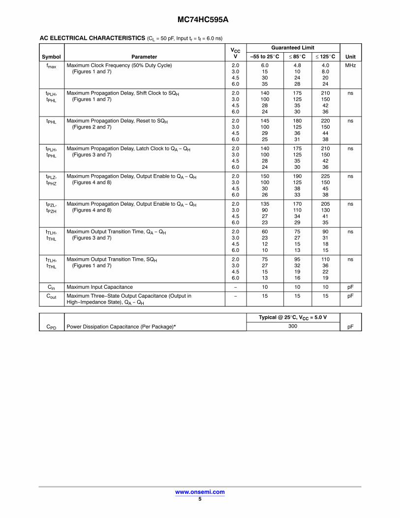
AC ELECTRICAL CHARACTERISTICS (CL = 50 pF, Input tr = tf = 6.0 ns)
Symbol ParameterVCC
V
Guaranteed Limit
Unit–55 to 25�C ≤ 85�C ≤ 125�C
fmax Maximum Clock Frequency (50% Duty Cycle)(Figures 1 and 7)
2.03.04.56.0
6.0153035
4.8102428
4.08.02024
MHz
tPLH,tPHL
Maximum Propagation Delay, Shift Clock to SQH(Figures 1 and 7)
2.03.04.56.0
1401002824
1751253530
2101504236
ns
tPHL Maximum Propagation Delay, Reset to SQH(Figures 2 and 7)
2.03.04.56.0
1451002925
1801253631
2201504438
ns
tPLH,tPHL
Maximum Propagation Delay, Latch Clock to QA − QH(Figures 3 and 7)
2.03.04.56.0
1401002824
1751253530
2101504236
ns
tPLZ,tPHZ
Maximum Propagation Delay, Output Enable to QA − QH(Figures 4 and 8)
2.03.04.56.0
1501003026
1901253833
2251504538
ns
tPZL,tPZH
Maximum Propagation Delay, Output Enable to QA − QH(Figures 4 and 8)
2.03.04.56.0
135902723
1701103429
2051304135
ns
tTLH,tTHL
Maximum Output Transition Time, QA − QH(Figures 3 and 7)
2.03.04.56.0
60231210
75271513
90311815
ns
tTLH,tTHL
Maximum Output Transition Time, SQH(Figures 1 and 7)
2.03.04.56.0
75271513
95321916
110362219
ns
Cin Maximum Input Capacitance − 10 10 10 pF
Cout Maximum Three−State Output Capacitance (Output inHigh−Impedance State), QA − QH
− 15 15 15 pF
CPD Power Dissipation Capacitance (Per Package)*
Typical @ 25°C, VCC = 5.0 V
pF300
MC74HC595A
www.onsemi.com6
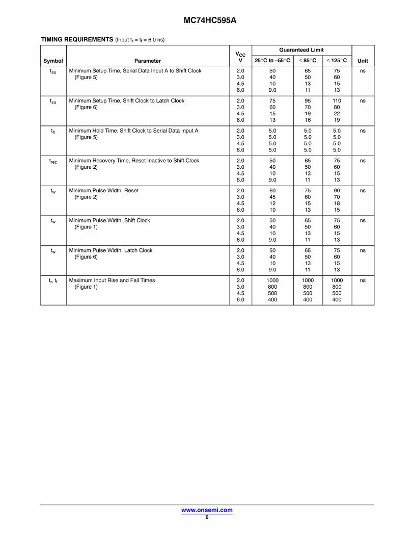
TIMING REQUIREMENTS (Input tr = tf = 6.0 ns)
Symbol ParameterVCC
V
Guaranteed Limit
Unit25�C to –55�C ≤ 85�C ≤ 125�C
tsu Minimum Setup Time, Serial Data Input A to Shift Clock(Figure 5)
2.03.04.56.0
5040109.0
65501311
75601513
ns
tsu Minimum Setup Time, Shift Clock to Latch Clock(Figure 6)
2.03.04.56.0
75601513
95701916
110802219
ns
th Minimum Hold Time, Shift Clock to Serial Data Input A(Figure 5)
2.03.04.56.0
5.05.05.05.0
5.05.05.05.0
5.05.05.05.0
ns
trec Minimum Recovery Time, Reset Inactive to Shift Clock(Figure 2)
2.03.04.56.0
5040109.0
65501311
75601513
ns
tw Minimum Pulse Width, Reset(Figure 2)
2.03.04.56.0
60451210
75601513
90701815
ns
tw Minimum Pulse Width, Shift Clock(Figure 1)
2.03.04.56.0
5040109.0
65501311
75601513
ns
tw Minimum Pulse Width, Latch Clock(Figure 6)
2.03.04.56.0
5040109.0
65501311
75601513
ns
tr, tf Maximum Input Rise and Fall Times(Figure 1)
2.03.04.56.0
1000800500400
1000800500400
1000800500400
ns
MC74HC595A
www.onsemi.com7
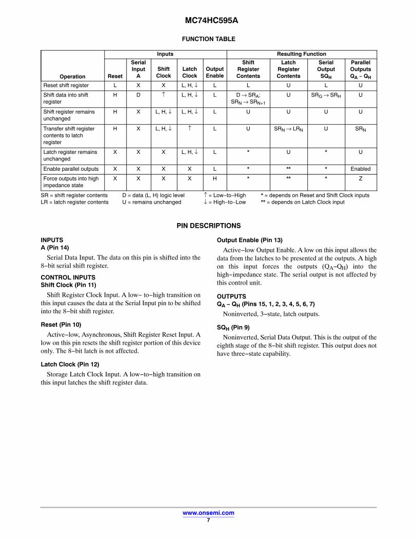
FUNCTION TABLE
Operation
Inputs Resulting Function
Reset
SerialInput
AShiftClock
LatchClock
OutputEnable
ShiftRegisterContents
LatchRegisterContents
SerialOutput
SQH
ParallelOutputsQA − QH
Reset shift register L X X L, H, ↓ L L U L U
Shift data into shiftregister
H D ↑ L, H, ↓ L D → SRA;SRN → SRN+1
U SRG → SRH U
Shift register remainsunchanged
H X L, H, ↓ L, H, ↓ L U U U U
Transfer shift registercontents to latchregister
H X L, H, ↓ ↑ L U SRN → LRN U SRN
Latch register remainsunchanged
X X X L, H, ↓ L * U * U
Enable parallel outputs X X X X L * ** * Enabled
Force outputs into highimpedance state
X X X X H * ** * Z
SR = shift register contents D = data (L, H) logic level ↑ = Low−to−High * = depends on Reset and Shift Clock inputsLR = latch register contents U = remains unchanged ↓ = High−to−Low ** = depends on Latch Clock input
PIN DESCRIPTIONS
INPUTSA (Pin 14)
Serial Data Input. The data on this pin is shifted into the8−bit serial shift register.
CONTROL INPUTSShift Clock (Pin 11)
Shift Register Clock Input. A low− to−high transition onthis input causes the data at the Serial Input pin to be shiftedinto the 8−bit shift register.
Reset (Pin 10)
Active−low, Asynchronous, Shift Register Reset Input. Alow on this pin resets the shift register portion of this deviceonly. The 8−bit latch is not affected.
Latch Clock (Pin 12)
Storage Latch Clock Input. A low−to−high transition onthis input latches the shift register data.
Output Enable (Pin 13)
Active−low Output Enable. A low on this input allows thedata from the latches to be presented at the outputs. A highon this input forces the outputs (QA−QH) into thehigh−impedance state. The serial output is not affected bythis control unit.
OUTPUTSQA − QH (Pins 15, 1, 2, 3, 4, 5, 6, 7)
Noninverted, 3−state, latch outputs.
SQH (Pin 9)
Noninverted, Serial Data Output. This is the output of theeighth stage of the 8−bit shift register. This output does nothave three−state capability.
MC74HC595A
www.onsemi.com8
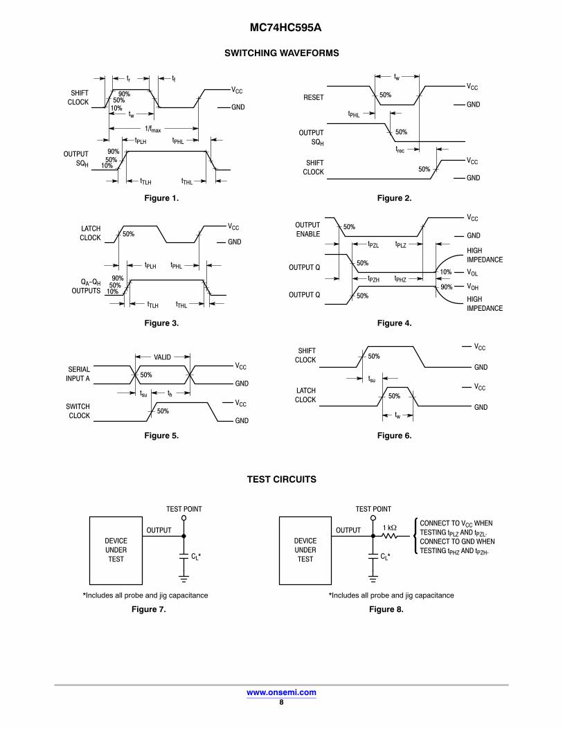
SWITCHING WAVEFORMS
SERIALINPUT A 50%
50%SWITCHCLOCK
VCC
GND
VALID
tsu th
Figure 5.
SHIFTCLOCK
OUTPUTSQH
tr tfVCC
GND
90%50%
10%
90%50%
10%
tPLH tPHL
tTLH tTHL
tw
1/fmax
RESET
OUTPUTSQH
SHIFTCLOCK
tw
50%
50%
50%
VCC
GND
VCC
GND
tPHL
trec
tsu
50%
50%
VCC
GND
LATCHCLOCK
QA-QHOUTPUTS
50%
tPLH tPHL
tTLH tTHL
90%50%
10%
VCC
GND
VCC
GND
SHIFTCLOCK
LATCHCLOCK
Figure 3.
VCC
GNDtw
Figure 1. Figure 2.
Figure 4.
Figure 6.
OUTPUT Q
OUTPUT Q
50%
50%
90%
10%
tPZL tPLZ
tPZH tPHZ
VCC
GND
HIGHIMPEDANCE
VOL
VOH
HIGHIMPEDANCE
OUTPUTENABLE
50%
TEST CIRCUITS
*Includes all probe and jig capacitance
CL*
TEST POINT
DEVICEUNDERTEST
OUTPUT
*Includes all probe and jig capacitance
CL*
TEST POINT
DEVICEUNDERTEST
OUTPUTCONNECT TO VCC WHENTESTING tPLZ AND tPZL.CONNECT TO GND WHENTESTING tPHZ AND tPZH.
1 k�
Figure 7. Figure 8.
MC74HC595A
www.onsemi.com9
D
R
Q
SRA
D Q
LRA
D Q
SRB
D Q
LRB
R
D Q
SRC
D Q
LRC
R
D Q
SRD
D Q
LRD
R
D Q
SRE
D Q
LRE
R
D Q
SRF
D Q
LRF
R
D Q
SRG
D Q
LRG
R
D Q
SRH
D Q
LRH
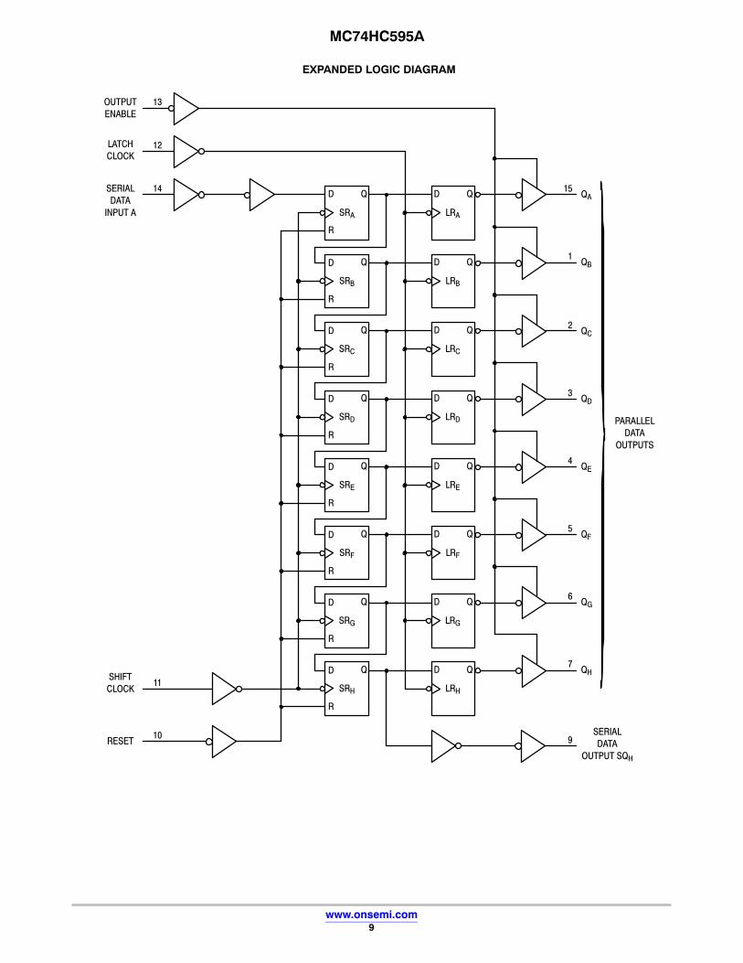
R
EXPANDED LOGIC DIAGRAM
OUTPUTENABLE
LATCHCLOCK
SERIALDATA
INPUT A
SHIFTCLOCK
RESET
13
12
14
11
10
15
1
2
3
4
5
6
7
9
QA
QB
QC
QD
QE
QF
QG
QH
SERIALDATA
OUTPUT SQH
PARALLELDATA
OUTPUTS
MC74HC595A
www.onsemi.com10
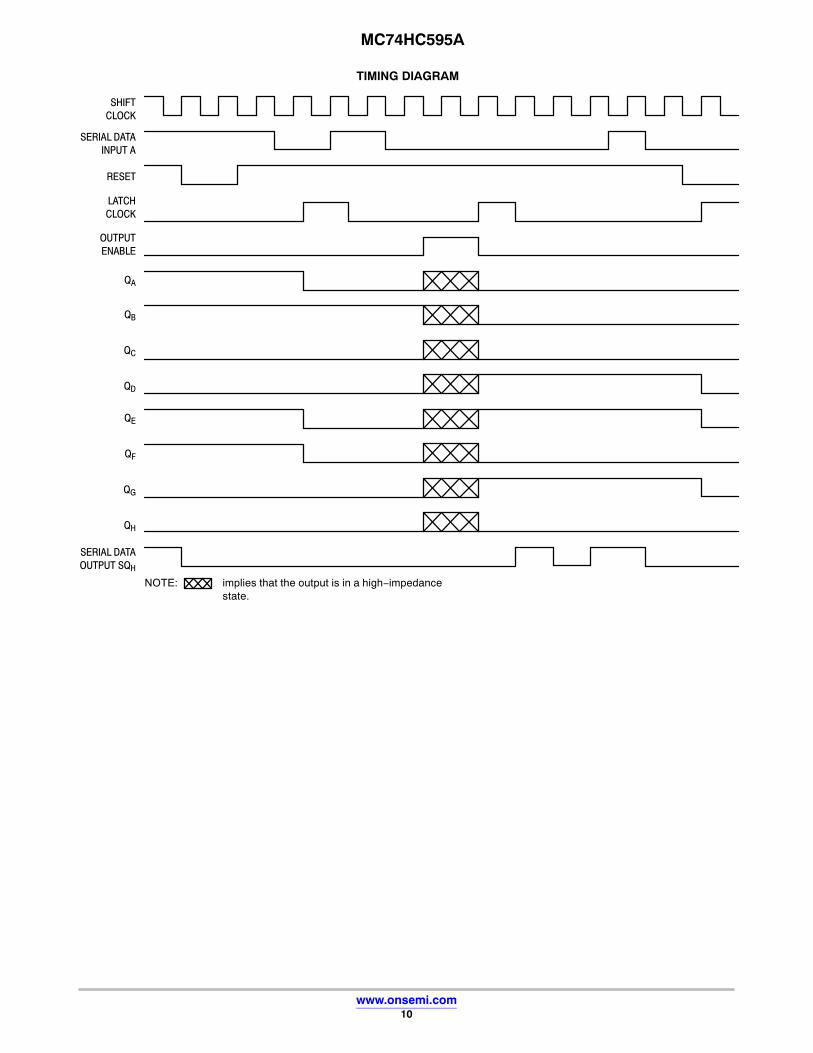
TIMING DIAGRAM
SHIFTCLOCK
SERIAL DATAINPUT A
RESET
LATCHCLOCK
OUTPUTENABLE
QA
QB
QC
QD
QE
QF
QG
QH
SERIAL DATAOUTPUT SQH
NOTE: implies that the output is in a high−impedancestate.
MC74HC595A
www.onsemi.com11
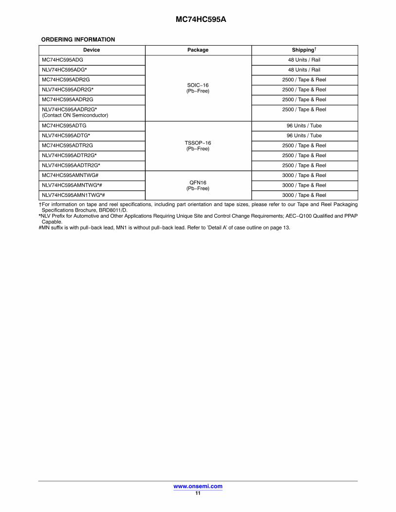
ORDERING INFORMATION
Device Package Shipping†
MC74HC595ADG
SOIC−16(Pb−Free)
48 Units / Rail
NLV74HC595ADG* 48 Units / Rail
MC74HC595ADR2G 2500 / Tape & Reel
NLV74HC595ADR2G* 2500 / Tape & Reel
MC74HC595AADR2G 2500 / Tape & Reel
NLV74HC595AADR2G*(Contact ON Semiconductor)
2500 / Tape & Reel
MC74HC595ADTG
TSSOP−16(Pb−Free)
96 Units / Tube
NLV74HC595ADTG* 96 Units / Tube
MC74HC595ADTR2G 2500 / Tape & Reel
NLV74HC595ADTR2G* 2500 / Tape & Reel
NLV74HC595AADTR2G* 2500 / Tape & Reel
MC74HC595AMNTWG#QFN16
(Pb−Free)
3000 / Tape & Reel
NLV74HC595AMNTWG*# 3000 / Tape & Reel
NLV74HC595AMN1TWG*# 3000 / Tape & Reel
†For information on tape and reel specifications, including part orientation and tape sizes, please refer to our Tape and Reel PackagingSpecifications Brochure, BRD8011/D.
*NLV Prefix for Automotive and Other Applications Requiring Unique Site and Control Change Requirements; AEC−Q100 Qualified and PPAPCapable.
#MN suffix is with pull−back lead, MN1 is without pull−back lead. Refer to ’Detail A’ of case outline on page 13.
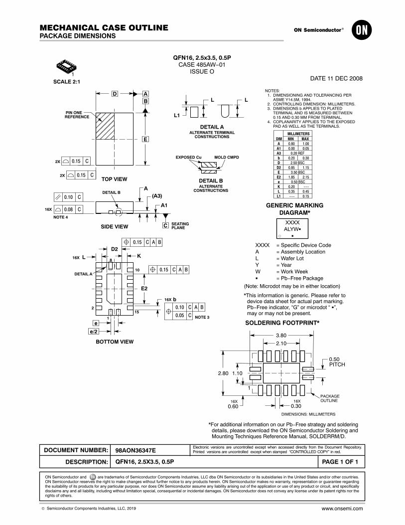
QFN16, 2.5x3.5, 0.5PCASE 485AW−01
ISSUE ODATE 11 DEC 2008
ÉÉÉÉÉÉÉÉÉ DIM MIN MAX
MILLIMETERS
AA1 0.00 0.05A3b 0.20 0.30D 2.50 BSCD2 0.85 1.15E 3.50 BSCE2e 0.50 BSCK 0.20 ---
NOTES:1. DIMENSIONING AND TOLERANCING PER
ASME Y14.5M, 1994.2. CONTROLLING DIMENSION: MILLIMETERS.3. DIMENSIONS b APPLIES TO PLATED
TERMINAL AND IS MEASURED BETWEEN0.15 AND 0.30 MM FROM TERMINAL.
4. COPLANARITY APPLIES TO THE EXPOSEDPAD AS WELL AS THE TERMINALS.
0.20 REF
b
D2
L
PIN ONE
E2
1
8
15
10
D
E
BA
C0.15
C0.15
2X
2X
e
2
16X
16X
0.10 C
0.05 C
A B
NOTE 3
A
16X
K
A1
(A3)
SEATINGPLANE
C0.08
C0.10
0.80 1.00
L 0.35 0.45
1.85 2.15
SCALE 2:1
GENERIC MARKINGDIAGRAM*
XXXX = Specific Device CodeA = Assembly LocationL = Wafer LotY = YearW = Work Week� = Pb−Free Package
XXXXALYW�
�
1
*This information is generic. Please refer todevice data sheet for actual part marking.Pb−Free indicator, “G” or microdot “ �”,may or may not be present.
L1
DETAIL A
L
ALTERNATE TERMINALCONSTRUCTIONS
L
ÇÇÇÇÇÇÉÉÉÉÉÉDETAIL B
MOLD CMPDEXPOSED Cu
ALTERNATECONSTRUCTIONSDETAIL B
*For additional information on our Pb−Free strategy and solderingdetails, please download the ON Semiconductor Soldering andMounting Techniques Reference Manual, SOLDERRM/D.
SOLDERING FOOTPRINT*
2.80
3.80
1.10
0.50
0.6016X
0.3016X
DIMENSIONS: MILLIMETERS
1
REFERENCE
TOP VIEW
SIDE VIEW
NOTE 4
C
0.15 C A B
0.15 C A BDETAIL A
BOTTOM VIEW
e/2
L1 --- 0.15
(Note: Microdot may be in either location)
2.10
PITCH
PACKAGEOUTLINE
MECHANICAL CASE OUTLINE
PACKAGE DIMENSIONS
ON Semiconductor and are trademarks of Semiconductor Components Industries, LLC dba ON Semiconductor or its subsidiaries in the United States and/or other countries.ON Semiconductor reserves the right to make changes without further notice to any products herein. ON Semiconductor makes no warranty, representation or guarantee regardingthe suitability of its products for any particular purpose, nor does ON Semiconductor assume any liability arising out of the application or use of any product or circuit, and specificallydisclaims any and all liability, including without limitation special, consequential or incidental damages. ON Semiconductor does not convey any license under its patent rights nor therights of others.
98AON36347EDOCUMENT NUMBER:
DESCRIPTION:
Electronic versions are uncontrolled except when accessed directly from the Document Repository.Printed versions are uncontrolled except when stamped “CONTROLLED COPY” in red.
PAGE 1 OF 1QFN16, 2.5X3.5, 0.5P
© Semiconductor Components Industries, LLC, 2019 www.onsemi.com
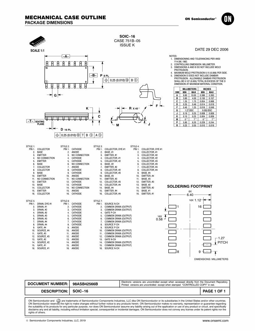
SOIC−16CASE 751B−05
ISSUE KDATE 29 DEC 2006SCALE 1:1
NOTES:1. DIMENSIONING AND TOLERANCING PER ANSI
Y14.5M, 1982.2. CONTROLLING DIMENSION: MILLIMETER.3. DIMENSIONS A AND B DO NOT INCLUDE MOLD
PROTRUSION.4. MAXIMUM MOLD PROTRUSION 0.15 (0.006) PER SIDE.5. DIMENSION D DOES NOT INCLUDE DAMBAR
PROTRUSION. ALLOWABLE DAMBAR PROTRUSIONSHALL BE 0.127 (0.005) TOTAL IN EXCESS OF THE DDIMENSION AT MAXIMUM MATERIAL CONDITION.
1 8
16 9
SEATINGPLANE
F
JM
R X 45�
G
8 PLP−B−
−A−
M0.25 (0.010) B S
−T−
D
K
C
16 PL
SBM0.25 (0.010) A ST
DIM MIN MAX MIN MAXINCHESMILLIMETERS
A 9.80 10.00 0.386 0.393B 3.80 4.00 0.150 0.157C 1.35 1.75 0.054 0.068D 0.35 0.49 0.014 0.019F 0.40 1.25 0.016 0.049G 1.27 BSC 0.050 BSCJ 0.19 0.25 0.008 0.009K 0.10 0.25 0.004 0.009M 0 7 0 7 P 5.80 6.20 0.229 0.244R 0.25 0.50 0.010 0.019
� � � �
6.40
16X0.58
16X 1.12
1.27
DIMENSIONS: MILLIMETERS
1
PITCH
SOLDERING FOOTPRINT
STYLE 1:PIN 1. COLLECTOR
2. BASE3. EMITTER4. NO CONNECTION5. EMITTER6. BASE7. COLLECTOR8. COLLECTOR9. BASE
10. EMITTER11. NO CONNECTION12. EMITTER13. BASE14. COLLECTOR15. EMITTER16. COLLECTOR
STYLE 2:PIN 1. CATHODE
2. ANODE3. NO CONNECTION4. CATHODE5. CATHODE6. NO CONNECTION7. ANODE8. CATHODE9. CATHODE
10. ANODE11. NO CONNECTION12. CATHODE13. CATHODE14. NO CONNECTION15. ANODE16. CATHODE
STYLE 3:PIN 1. COLLECTOR, DYE #1
2. BASE, #13. EMITTER, #14. COLLECTOR, #15. COLLECTOR, #26. BASE, #27. EMITTER, #28. COLLECTOR, #29. COLLECTOR, #3
10. BASE, #311. EMITTER, #312. COLLECTOR, #313. COLLECTOR, #414. BASE, #415. EMITTER, #416. COLLECTOR, #4
STYLE 4:PIN 1. COLLECTOR, DYE #1
2. COLLECTOR, #13. COLLECTOR, #24. COLLECTOR, #25. COLLECTOR, #36. COLLECTOR, #37. COLLECTOR, #48. COLLECTOR, #49. BASE, #4
10. EMITTER, #411. BASE, #312. EMITTER, #313. BASE, #214. EMITTER, #215. BASE, #116. EMITTER, #1
STYLE 5:PIN 1. DRAIN, DYE #1
2. DRAIN, #13. DRAIN, #24. DRAIN, #25. DRAIN, #36. DRAIN, #37. DRAIN, #48. DRAIN, #49. GATE, #4
10. SOURCE, #411. GATE, #312. SOURCE, #313. GATE, #214. SOURCE, #215. GATE, #116. SOURCE, #1
STYLE 6:PIN 1. CATHODE
2. CATHODE3. CATHODE4. CATHODE5. CATHODE6. CATHODE7. CATHODE8. CATHODE9. ANODE
10. ANODE11. ANODE12. ANODE13. ANODE14. ANODE15. ANODE16. ANODE
STYLE 7:PIN 1. SOURCE N‐CH
2. COMMON DRAIN (OUTPUT)3. COMMON DRAIN (OUTPUT)4. GATE P‐CH5. COMMON DRAIN (OUTPUT)6. COMMON DRAIN (OUTPUT)7. COMMON DRAIN (OUTPUT)8. SOURCE P‐CH9. SOURCE P‐CH
10. COMMON DRAIN (OUTPUT)11. COMMON DRAIN (OUTPUT)12. COMMON DRAIN (OUTPUT)13. GATE N‐CH14. COMMON DRAIN (OUTPUT)15. COMMON DRAIN (OUTPUT)16. SOURCE N‐CH
16
8 9
8X
MECHANICAL CASE OUTLINE
PACKAGE DIMENSIONS
ON Semiconductor and are trademarks of Semiconductor Components Industries, LLC dba ON Semiconductor or its subsidiaries in the United States and/or other countries.ON Semiconductor reserves the right to make changes without further notice to any products herein. ON Semiconductor makes no warranty, representation or guarantee regardingthe suitability of its products for any particular purpose, nor does ON Semiconductor assume any liability arising out of the application or use of any product or circuit, and specificallydisclaims any and all liability, including without limitation special, consequential or incidental damages. ON Semiconductor does not convey any license under its patent rights nor therights of others.
98ASB42566BDOCUMENT NUMBER:
DESCRIPTION:
Electronic versions are uncontrolled except when accessed directly from the Document Repository.Printed versions are uncontrolled except when stamped “CONTROLLED COPY” in red.
PAGE 1 OF 1SOIC−16
© Semiconductor Components Industries, LLC, 2019 www.onsemi.com
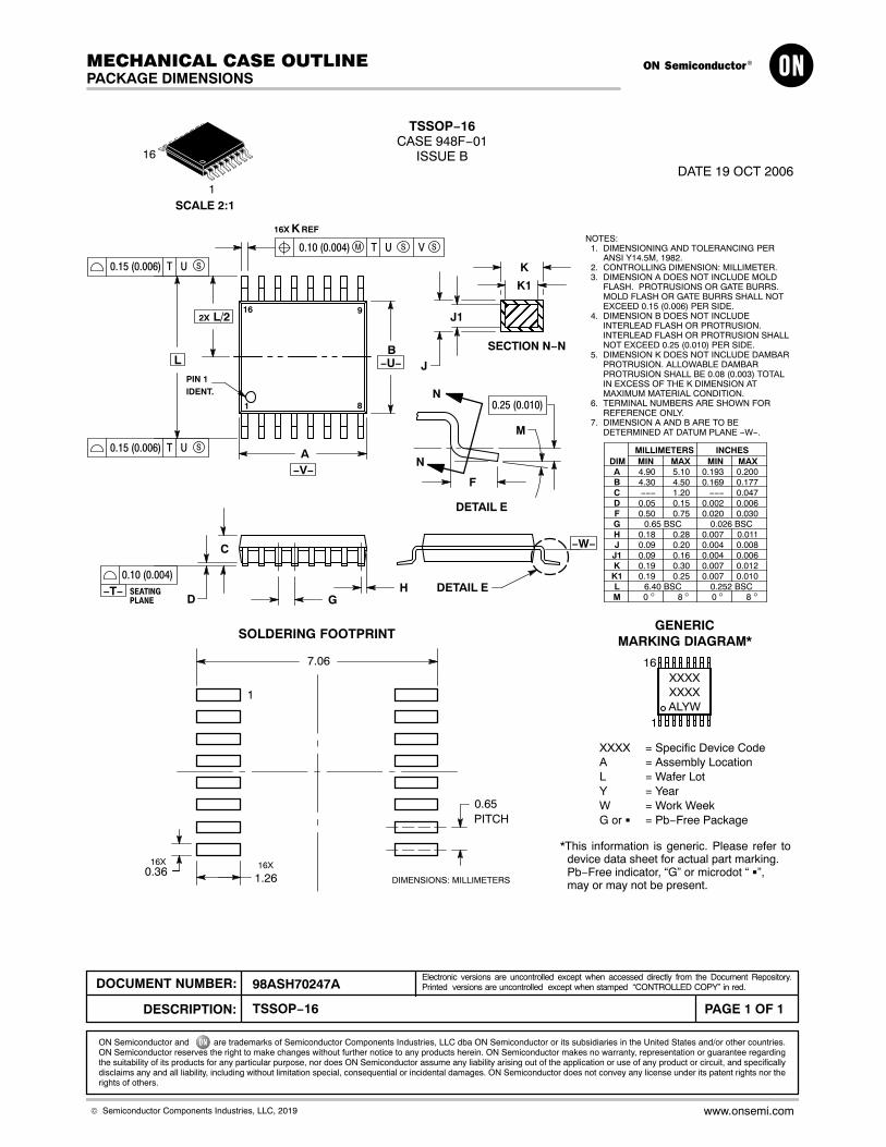
TSSOP−16CASE 948F−01
ISSUE BDATE 19 OCT 2006
SCALE 2:1
ÇÇÇÇÇÇ
DIM MIN MAX MIN MAXINCHESMILLIMETERS
A 4.90 5.10 0.193 0.200B 4.30 4.50 0.169 0.177C −−− 1.20 −−− 0.047D 0.05 0.15 0.002 0.006F 0.50 0.75 0.020 0.030G 0.65 BSC 0.026 BSCH 0.18 0.28 0.007 0.011J 0.09 0.20 0.004 0.008
J1 0.09 0.16 0.004 0.006K 0.19 0.30 0.007 0.012K1 0.19 0.25 0.007 0.010L 6.40 BSC 0.252 BSCM 0 8 0 8
NOTES:1. DIMENSIONING AND TOLERANCING PER
ANSI Y14.5M, 1982.2. CONTROLLING DIMENSION: MILLIMETER.3. DIMENSION A DOES NOT INCLUDE MOLD
FLASH. PROTRUSIONS OR GATE BURRS.MOLD FLASH OR GATE BURRS SHALL NOTEXCEED 0.15 (0.006) PER SIDE.
4. DIMENSION B DOES NOT INCLUDEINTERLEAD FLASH OR PROTRUSION.INTERLEAD FLASH OR PROTRUSION SHALLNOT EXCEED 0.25 (0.010) PER SIDE.
5. DIMENSION K DOES NOT INCLUDE DAMBARPROTRUSION. ALLOWABLE DAMBARPROTRUSION SHALL BE 0.08 (0.003) TOTALIN EXCESS OF THE K DIMENSION ATMAXIMUM MATERIAL CONDITION.
6. TERMINAL NUMBERS ARE SHOWN FORREFERENCE ONLY.
7. DIMENSION A AND B ARE TO BEDETERMINED AT DATUM PLANE −W−.
� � � �
SECTION N−N
SEATINGPLANE
IDENT.PIN 1
1 8
16 9
DETAIL E
J
J1
B
C
D
A
K
K1
HG
ÉÉÉÉÉÉ
DETAIL E
F
M
L
2X L/2
−U−
SU0.15 (0.006) T
SU0.15 (0.006) T
SUM0.10 (0.004) V ST
0.10 (0.004)−T−
−V−
−W−
0.25 (0.010)
16X REFK
N
N
1
16
GENERICMARKING DIAGRAM*
XXXXXXXXALYW
1
16
*This information is generic. Please refer todevice data sheet for actual part marking.Pb−Free indicator, “G” or microdot “ �”,may or may not be present.
XXXX = Specific Device CodeA = Assembly LocationL = Wafer LotY = YearW = Work WeekG or � = Pb−Free Package
7.06
16X0.36
16X
1.26
0.65
DIMENSIONS: MILLIMETERS
1
PITCH
SOLDERING FOOTPRINT
MECHANICAL CASE OUTLINE
PACKAGE DIMENSIONS
ON Semiconductor and are trademarks of Semiconductor Components Industries, LLC dba ON Semiconductor or its subsidiaries in the United States and/or other countries.ON Semiconductor reserves the right to make changes without further notice to any products herein. ON Semiconductor makes no warranty, representation or guarantee regardingthe suitability of its products for any particular purpose, nor does ON Semiconductor assume any liability arising out of the application or use of any product or circuit, and specificallydisclaims any and all liability, including without limitation special, consequential or incidental damages. ON Semiconductor does not convey any license under its patent rights nor therights of others.
98ASH70247ADOCUMENT NUMBER:
DESCRIPTION:
Electronic versions are uncontrolled except when accessed directly from the Document Repository.Printed versions are uncontrolled except when stamped “CONTROLLED COPY” in red.
PAGE 1 OF 1TSSOP−16
© Semiconductor Components Industries, LLC, 2019 www.onsemi.com
onsemi, , and other names, marks, and brands are registered and/or common law trademarks of Semiconductor Components Industries, LLC dba “onsemi” or its affiliatesand/or subsidiaries in the United States and/or other countries. onsemi owns the rights to a number of patents, trademarks, copyrights, trade secrets, and other intellectual property.A listing of onsemi’s product/patent coverage may be accessed at www.onsemi.com/site/pdf/Patent−Marking.pdf. onsemi reserves the right to make changes at any time to anyproducts or information herein, without notice. The information herein is provided “as−is” and onsemi makes no warranty, representation or guarantee regarding the accuracy of theinformation, product features, availability, functionality, or suitability of its products for any particular purpose, nor does onsemi assume any liability arising out of the application or useof any product or circuit, and specifically disclaims any and all liability, including without limitation special, consequential or incidental damages. Buyer is responsible for its productsand applications using onsemi products, including compliance with all laws, regulations and safety requirements or standards, regardless of any support or applications informationprovided by onsemi. “Typical” parameters which may be provided in onsemi data sheets and/or specifications can and do vary in different applications and actual performance mayvary over time. All operating parameters, including “Typicals” must be validated for each customer application by customer’s technical experts. onsemi does not convey any licenseunder any of its intellectual property rights nor the rights of others. onsemi products are not designed, intended, or authorized for use as a critical component in life support systemsor any FDA Class 3 medical devices or medical devices with a same or similar classification in a foreign jurisdiction or any devices intended for implantation in the human body. ShouldBuyer purchase or use onsemi products for any such unintended or unauthorized application, Buyer shall indemnify and hold onsemi and its officers, employees, subsidiaries, affiliates,and distributors harmless against all claims, costs, damages, and expenses, and reasonable attorney fees arising out of, directly or indirectly, any claim of personal injury or deathassociated with such unintended or unauthorized use, even if such claim alleges that onsemi was negligent regarding the design or manufacture of the part. onsemi is an EqualOpportunity/Affirmative Action Employer. This literature is subject to all applicable copyright laws and is not for resale in any manner.
PUBLICATION ORDERING INFORMATIONTECHNICAL SUPPORTNorth American Technical Support:Voice Mail: 1 800−282−9855 Toll Free USA/CanadaPhone: 011 421 33 790 2910
LITERATURE FULFILLMENT:Email Requests to: [email protected]
onsemi Website: www.onsemi.com
Europe, Middle East and Africa Technical Support:Phone: 00421 33 790 2910For additional information, please contact your local Sales Representative
◊
Related Documents


![74HC164; 74HCT164 8-bit serial-in, parallel-out shift register · 8-bit serial-in, parallel-out shift register [1] The input and output voltage ratings may be exceeded if the input](https://static.cupdf.com/doc/110x72/5ce599c888c993b62d8bbe66/74hc164-74hct164-8-bit-serial-in-parallel-out-shift-register-8-bit-serial-in.jpg)