M68HC05 Microcontrollers freescale.com MC68HC05P4A Data Sheet MC68HC05P4A Rev. 7.1 9/2005

Welcome message from author
This document is posted to help you gain knowledge. Please leave a comment to let me know what you think about it! Share it to your friends and learn new things together.
Transcript
M68HC05Microcontrollers
freescale.com
MC68HC05P4A
Data Sheet
MC68HC05P4ARev. 7.19/2005

Blank
MC68HC05P4A Data Sheet, Rev. 7.1
Freescale Semiconductor 3
Freescale™ and the Freescale logo are trademarks of Freescale Semiconductor, Inc.
© Freescale Semiconductor, Inc., 2005. All rights reserved.
MC68HC05P4AData Sheet
To provide the most up-to-date information, the revision of our documents on the World Wide Web will be the most current. Your printed copy may be an earlier revision. To verify you have the latest information available, refer to:
http://www.freescale.com/
The following revision history table summarizes changes contained in this document. For your convenience, the page number designators have been linked to the appropriate location.
Revision History
DateRevision
LevelDescription
PageNumber(s)
May,2002
7.0 Corrected World Wide Web address and qualification status N/A
September,2005
7.1 Updated to meet Freescale identity guidelines. Throughout

MC68HC05P4A Data Sheet, Rev. 7.1
4 Freescale Semiconductor
MC68HC05P4A Data Sheet, Rev. 7.1
Freescale Semiconductor 5
List of Chapters
Chapter 1 General Description. . . . . . . . . . . . . . . . . . . . . . . . . . . . . . . . . . . . . . . . . . . . . . . .11
Chapter 2 Memory Map. . . . . . . . . . . . . . . . . . . . . . . . . . . . . . . . . . . . . . . . . . . . . . . . . . . . . .17
Chapter 3 Central Processor Unit (CPU). . . . . . . . . . . . . . . . . . . . . . . . . . . . . . . . . . . . . . . .21
Chapter 4 Interrupts . . . . . . . . . . . . . . . . . . . . . . . . . . . . . . . . . . . . . . . . . . . . . . . . . . . . . . . .23
Chapter 5 Resets. . . . . . . . . . . . . . . . . . . . . . . . . . . . . . . . . . . . . . . . . . . . . . . . . . . . . . . . . . .27
Chapter 6 Low-Power Modes . . . . . . . . . . . . . . . . . . . . . . . . . . . . . . . . . . . . . . . . . . . . . . . . .29
Chapter 7 Simple Serial Input/Output Port (SIOP) . . . . . . . . . . . . . . . . . . . . . . . . . . . . . . . .31
Chapter 8 Timer . . . . . . . . . . . . . . . . . . . . . . . . . . . . . . . . . . . . . . . . . . . . . . . . . . . . . . . . . . . .35
Chapter 9 Computer Operating Properly (COP) . . . . . . . . . . . . . . . . . . . . . . . . . . . . . . . . . .41
Chapter 10 Self-Check Mode . . . . . . . . . . . . . . . . . . . . . . . . . . . . . . . . . . . . . . . . . . . . . . . . .43
Chapter 11 Instruction Set . . . . . . . . . . . . . . . . . . . . . . . . . . . . . . . . . . . . . . . . . . . . . . . . . . .45
Chapter 12 Electrical Specifications . . . . . . . . . . . . . . . . . . . . . . . . . . . . . . . . . . . . . . . . . . .59
Chapter 13 Mechanical Specifications . . . . . . . . . . . . . . . . . . . . . . . . . . . . . . . . . . . . . . . . .67
Chapter 14 Ordering Information. . . . . . . . . . . . . . . . . . . . . . . . . . . . . . . . . . . . . . . . . . . . . .69

List of Chapters
MC68HC05P4A Data Sheet, Rev. 7.1
6 Freescale Semiconductor
MC68HC05P4A Data Sheet, Rev. 7.1
Freescale Semiconductor 7
Table of Contents
Chapter 1 General Description
1.1 Introduction . . . . . . . . . . . . . . . . . . . . . . . . . . . . . . . . . . . . . . . . . . . . . . . . . . . . . . . . . . . . . . . . 111.2 Features. . . . . . . . . . . . . . . . . . . . . . . . . . . . . . . . . . . . . . . . . . . . . . . . . . . . . . . . . . . . . . . . . . . 111.3 Mask Options . . . . . . . . . . . . . . . . . . . . . . . . . . . . . . . . . . . . . . . . . . . . . . . . . . . . . . . . . . . . . . . 121.4 MCU Structure . . . . . . . . . . . . . . . . . . . . . . . . . . . . . . . . . . . . . . . . . . . . . . . . . . . . . . . . . . . . . . 121.5 Pin Assignments . . . . . . . . . . . . . . . . . . . . . . . . . . . . . . . . . . . . . . . . . . . . . . . . . . . . . . . . . . . . 141.6 Signal Description . . . . . . . . . . . . . . . . . . . . . . . . . . . . . . . . . . . . . . . . . . . . . . . . . . . . . . . . . . . 141.6.1 VDD and VSS . . . . . . . . . . . . . . . . . . . . . . . . . . . . . . . . . . . . . . . . . . . . . . . . . . . . . . . . . . . . 141.6.2 IRQ . . . . . . . . . . . . . . . . . . . . . . . . . . . . . . . . . . . . . . . . . . . . . . . . . . . . . . . . . . . . . . . . . . . 141.6.3 OSC1 and OSC2 . . . . . . . . . . . . . . . . . . . . . . . . . . . . . . . . . . . . . . . . . . . . . . . . . . . . . . . . . 141.6.4 RESET . . . . . . . . . . . . . . . . . . . . . . . . . . . . . . . . . . . . . . . . . . . . . . . . . . . . . . . . . . . . . . . . 151.6.5 TCMP. . . . . . . . . . . . . . . . . . . . . . . . . . . . . . . . . . . . . . . . . . . . . . . . . . . . . . . . . . . . . . . . . . 151.6.6 PA0–PA7 . . . . . . . . . . . . . . . . . . . . . . . . . . . . . . . . . . . . . . . . . . . . . . . . . . . . . . . . . . . . . . . 151.6.7 SDO/PB5, SDI/PB6, and SCK/PB7 . . . . . . . . . . . . . . . . . . . . . . . . . . . . . . . . . . . . . . . . . . . 151.6.8 PC0–PC7 . . . . . . . . . . . . . . . . . . . . . . . . . . . . . . . . . . . . . . . . . . . . . . . . . . . . . . . . . . . . . . . 151.6.9 PD5 and TCAP/PD7. . . . . . . . . . . . . . . . . . . . . . . . . . . . . . . . . . . . . . . . . . . . . . . . . . . . . . . 161.7 Input/Output Programming. . . . . . . . . . . . . . . . . . . . . . . . . . . . . . . . . . . . . . . . . . . . . . . . . . . . . 16
Chapter 2 Memory Map
2.1 Introduction . . . . . . . . . . . . . . . . . . . . . . . . . . . . . . . . . . . . . . . . . . . . . . . . . . . . . . . . . . . . . . . . 172.2 ROM. . . . . . . . . . . . . . . . . . . . . . . . . . . . . . . . . . . . . . . . . . . . . . . . . . . . . . . . . . . . . . . . . . . . . . 202.3 ROM Security Feature . . . . . . . . . . . . . . . . . . . . . . . . . . . . . . . . . . . . . . . . . . . . . . . . . . . . . . . . 202.4 RAM . . . . . . . . . . . . . . . . . . . . . . . . . . . . . . . . . . . . . . . . . . . . . . . . . . . . . . . . . . . . . . . . . . . . . . 20
Chapter 3 Central Processor Unit (CPU)
3.1 Introduction . . . . . . . . . . . . . . . . . . . . . . . . . . . . . . . . . . . . . . . . . . . . . . . . . . . . . . . . . . . . . . . . 213.2 Accumulator (A) . . . . . . . . . . . . . . . . . . . . . . . . . . . . . . . . . . . . . . . . . . . . . . . . . . . . . . . . . . . . . 213.3 Index Register (X) . . . . . . . . . . . . . . . . . . . . . . . . . . . . . . . . . . . . . . . . . . . . . . . . . . . . . . . . . . . 213.4 Condition Code Register (CCR). . . . . . . . . . . . . . . . . . . . . . . . . . . . . . . . . . . . . . . . . . . . . . . . . 213.4.1 H — Half Carry. . . . . . . . . . . . . . . . . . . . . . . . . . . . . . . . . . . . . . . . . . . . . . . . . . . . . . . . . . . 213.4.2 I — Interrupt . . . . . . . . . . . . . . . . . . . . . . . . . . . . . . . . . . . . . . . . . . . . . . . . . . . . . . . . . . . . . 213.4.3 N — Negative. . . . . . . . . . . . . . . . . . . . . . . . . . . . . . . . . . . . . . . . . . . . . . . . . . . . . . . . . . . . 213.4.4 Z — Zero . . . . . . . . . . . . . . . . . . . . . . . . . . . . . . . . . . . . . . . . . . . . . . . . . . . . . . . . . . . . . . . 223.4.5 C — Carry/Borrow . . . . . . . . . . . . . . . . . . . . . . . . . . . . . . . . . . . . . . . . . . . . . . . . . . . . . . . . 223.5 Stack Pointer (SP) . . . . . . . . . . . . . . . . . . . . . . . . . . . . . . . . . . . . . . . . . . . . . . . . . . . . . . . . . . . 223.6 Program Counter (PC) . . . . . . . . . . . . . . . . . . . . . . . . . . . . . . . . . . . . . . . . . . . . . . . . . . . . . . . . 22
Table of Contents
MC68HC05P4A Data Sheet, Rev. 7.1
8 Freescale Semiconductor
Chapter 4 Interrupts
4.1 Introduction . . . . . . . . . . . . . . . . . . . . . . . . . . . . . . . . . . . . . . . . . . . . . . . . . . . . . . . . . . . . . . . . 234.2 Hardware Controlled Interrupt Sequence . . . . . . . . . . . . . . . . . . . . . . . . . . . . . . . . . . . . . . . . . 234.3 Timer Interrupt . . . . . . . . . . . . . . . . . . . . . . . . . . . . . . . . . . . . . . . . . . . . . . . . . . . . . . . . . . . . . . 254.4 External Interrupt . . . . . . . . . . . . . . . . . . . . . . . . . . . . . . . . . . . . . . . . . . . . . . . . . . . . . . . . . . . . 254.5 Optional External Interrupts (PA0–PA7) . . . . . . . . . . . . . . . . . . . . . . . . . . . . . . . . . . . . . . . . . . 264.6 Software Interrupt (SWI) . . . . . . . . . . . . . . . . . . . . . . . . . . . . . . . . . . . . . . . . . . . . . . . . . . . . . . 26
Chapter 5 Resets
5.1 Introduction . . . . . . . . . . . . . . . . . . . . . . . . . . . . . . . . . . . . . . . . . . . . . . . . . . . . . . . . . . . . . . . . 275.2 Power-On Reset (POR) . . . . . . . . . . . . . . . . . . . . . . . . . . . . . . . . . . . . . . . . . . . . . . . . . . . . . . . 275.3 RESET Pin. . . . . . . . . . . . . . . . . . . . . . . . . . . . . . . . . . . . . . . . . . . . . . . . . . . . . . . . . . . . . . . . . 275.4 Computer Operating Properly (COP) Reset . . . . . . . . . . . . . . . . . . . . . . . . . . . . . . . . . . . . . . . 27
Chapter 6 Low-Power Modes
6.1 Introduction . . . . . . . . . . . . . . . . . . . . . . . . . . . . . . . . . . . . . . . . . . . . . . . . . . . . . . . . . . . . . . . . 296.2 Stop Mode . . . . . . . . . . . . . . . . . . . . . . . . . . . . . . . . . . . . . . . . . . . . . . . . . . . . . . . . . . . . . . . . . 296.3 WAIT Instruction . . . . . . . . . . . . . . . . . . . . . . . . . . . . . . . . . . . . . . . . . . . . . . . . . . . . . . . . . . . . 29
Chapter 7 Simple Serial Input/Output Port (SIOP)
7.1 Introduction . . . . . . . . . . . . . . . . . . . . . . . . . . . . . . . . . . . . . . . . . . . . . . . . . . . . . . . . . . . . . . . . 317.2 Signal Format. . . . . . . . . . . . . . . . . . . . . . . . . . . . . . . . . . . . . . . . . . . . . . . . . . . . . . . . . . . . . . . 317.2.1 Serial Clock (SCK) . . . . . . . . . . . . . . . . . . . . . . . . . . . . . . . . . . . . . . . . . . . . . . . . . . . . . . . . 317.2.2 Serial Data Out (SDO) . . . . . . . . . . . . . . . . . . . . . . . . . . . . . . . . . . . . . . . . . . . . . . . . . . . . . 327.2.3 Serial Data In (SDI) . . . . . . . . . . . . . . . . . . . . . . . . . . . . . . . . . . . . . . . . . . . . . . . . . . . . . . . 327.3 SIOP Registers . . . . . . . . . . . . . . . . . . . . . . . . . . . . . . . . . . . . . . . . . . . . . . . . . . . . . . . . . . . . . 327.3.1 SIOP Control Register . . . . . . . . . . . . . . . . . . . . . . . . . . . . . . . . . . . . . . . . . . . . . . . . . . . . . 327.3.2 SIOP Status Register . . . . . . . . . . . . . . . . . . . . . . . . . . . . . . . . . . . . . . . . . . . . . . . . . . . . . . 337.3.3 SIOP Data Register . . . . . . . . . . . . . . . . . . . . . . . . . . . . . . . . . . . . . . . . . . . . . . . . . . . . . . . 34
Chapter 8 Timer
8.1 Introduction . . . . . . . . . . . . . . . . . . . . . . . . . . . . . . . . . . . . . . . . . . . . . . . . . . . . . . . . . . . . . . . . 358.2 Counter . . . . . . . . . . . . . . . . . . . . . . . . . . . . . . . . . . . . . . . . . . . . . . . . . . . . . . . . . . . . . . . . . . . 368.3 Output Compare Register . . . . . . . . . . . . . . . . . . . . . . . . . . . . . . . . . . . . . . . . . . . . . . . . . . . . . 368.4 Input Capture Register. . . . . . . . . . . . . . . . . . . . . . . . . . . . . . . . . . . . . . . . . . . . . . . . . . . . . . . . 378.5 Timer Control Register . . . . . . . . . . . . . . . . . . . . . . . . . . . . . . . . . . . . . . . . . . . . . . . . . . . . . . . . 378.6 Timer Status Register . . . . . . . . . . . . . . . . . . . . . . . . . . . . . . . . . . . . . . . . . . . . . . . . . . . . . . . . 388.7 Timer During Wait or Halt Mode . . . . . . . . . . . . . . . . . . . . . . . . . . . . . . . . . . . . . . . . . . . . . . . . 398.8 Timer During Stop Mode . . . . . . . . . . . . . . . . . . . . . . . . . . . . . . . . . . . . . . . . . . . . . . . . . . . . . . 39
Table of Contents
MC68HC05P4A Data Sheet, Rev. 7.1
Freescale Semiconductor 9
Chapter 9 Computer Operating Properly (COP)
9.1 Introduction . . . . . . . . . . . . . . . . . . . . . . . . . . . . . . . . . . . . . . . . . . . . . . . . . . . . . . . . . . . . . . . . 419.2 Resetting the COP . . . . . . . . . . . . . . . . . . . . . . . . . . . . . . . . . . . . . . . . . . . . . . . . . . . . . . . . . . . 419.3 COP During Wait or Halt Mode . . . . . . . . . . . . . . . . . . . . . . . . . . . . . . . . . . . . . . . . . . . . . . . . . 419.4 COP During Stop Mode . . . . . . . . . . . . . . . . . . . . . . . . . . . . . . . . . . . . . . . . . . . . . . . . . . . . . . . 41
Chapter 10 Self-Check Mode
10.1 Introduction . . . . . . . . . . . . . . . . . . . . . . . . . . . . . . . . . . . . . . . . . . . . . . . . . . . . . . . . . . . . . . . . 4310.2 Functional Description . . . . . . . . . . . . . . . . . . . . . . . . . . . . . . . . . . . . . . . . . . . . . . . . . . . . . . . . 43
Chapter 11 Instruction Set
11.1 Introduction . . . . . . . . . . . . . . . . . . . . . . . . . . . . . . . . . . . . . . . . . . . . . . . . . . . . . . . . . . . . . . . . 4511.2 Addressing Modes . . . . . . . . . . . . . . . . . . . . . . . . . . . . . . . . . . . . . . . . . . . . . . . . . . . . . . . . . . . 4511.2.1 Inherent . . . . . . . . . . . . . . . . . . . . . . . . . . . . . . . . . . . . . . . . . . . . . . . . . . . . . . . . . . . . . . . . 4511.2.2 Immediate . . . . . . . . . . . . . . . . . . . . . . . . . . . . . . . . . . . . . . . . . . . . . . . . . . . . . . . . . . . . . . 4511.2.3 Direct . . . . . . . . . . . . . . . . . . . . . . . . . . . . . . . . . . . . . . . . . . . . . . . . . . . . . . . . . . . . . . . . . . 4511.2.4 Extended . . . . . . . . . . . . . . . . . . . . . . . . . . . . . . . . . . . . . . . . . . . . . . . . . . . . . . . . . . . . . . . 4611.2.5 Indexed, No Offset . . . . . . . . . . . . . . . . . . . . . . . . . . . . . . . . . . . . . . . . . . . . . . . . . . . . . . . . 4611.2.6 Indexed, 8-Bit Offset . . . . . . . . . . . . . . . . . . . . . . . . . . . . . . . . . . . . . . . . . . . . . . . . . . . . . . 4611.2.7 Indexed, 16-Bit Offset . . . . . . . . . . . . . . . . . . . . . . . . . . . . . . . . . . . . . . . . . . . . . . . . . . . . . 4611.2.8 Relative . . . . . . . . . . . . . . . . . . . . . . . . . . . . . . . . . . . . . . . . . . . . . . . . . . . . . . . . . . . . . . . . 4611.3 Instruction Types . . . . . . . . . . . . . . . . . . . . . . . . . . . . . . . . . . . . . . . . . . . . . . . . . . . . . . . . . . . . 4711.3.1 Register/Memory Instructions . . . . . . . . . . . . . . . . . . . . . . . . . . . . . . . . . . . . . . . . . . . . . . . 4711.3.2 Read-Modify-Write Instructions . . . . . . . . . . . . . . . . . . . . . . . . . . . . . . . . . . . . . . . . . . . . . . 4811.3.3 Jump/Branch Instructions. . . . . . . . . . . . . . . . . . . . . . . . . . . . . . . . . . . . . . . . . . . . . . . . . . . 4911.3.4 Bit Manipulation Instructions . . . . . . . . . . . . . . . . . . . . . . . . . . . . . . . . . . . . . . . . . . . . . . . . 5011.3.5 Control Instructions . . . . . . . . . . . . . . . . . . . . . . . . . . . . . . . . . . . . . . . . . . . . . . . . . . . . . . . 5011.4 Instruction Set Summary . . . . . . . . . . . . . . . . . . . . . . . . . . . . . . . . . . . . . . . . . . . . . . . . . . . . . . 5111.5 Opcode Map . . . . . . . . . . . . . . . . . . . . . . . . . . . . . . . . . . . . . . . . . . . . . . . . . . . . . . . . . . . . . . . 56
Chapter 12 Electrical Specifications
12.1 Introduction . . . . . . . . . . . . . . . . . . . . . . . . . . . . . . . . . . . . . . . . . . . . . . . . . . . . . . . . . . . . . . . . 5912.2 Maximum Ratings . . . . . . . . . . . . . . . . . . . . . . . . . . . . . . . . . . . . . . . . . . . . . . . . . . . . . . . . . . . 5912.3 Operating Range . . . . . . . . . . . . . . . . . . . . . . . . . . . . . . . . . . . . . . . . . . . . . . . . . . . . . . . . . . . . 5912.4 Thermal Characteristics . . . . . . . . . . . . . . . . . . . . . . . . . . . . . . . . . . . . . . . . . . . . . . . . . . . . . . . 5912.5 5.0-Volt DC Electrical Characteristics . . . . . . . . . . . . . . . . . . . . . . . . . . . . . . . . . . . . . . . . . . . . 6012.6 3.3-Volt DC Electrical Characteristics . . . . . . . . . . . . . . . . . . . . . . . . . . . . . . . . . . . . . . . . . . . . 6112.7 5.0-Volt SIOP Timing . . . . . . . . . . . . . . . . . . . . . . . . . . . . . . . . . . . . . . . . . . . . . . . . . . . . . . . . . 6212.8 3.3-Volt SIOP Timing . . . . . . . . . . . . . . . . . . . . . . . . . . . . . . . . . . . . . . . . . . . . . . . . . . . . . . . . . 6212.9 5.0-Volt Control Timing . . . . . . . . . . . . . . . . . . . . . . . . . . . . . . . . . . . . . . . . . . . . . . . . . . . . . . . 6312.10 3.3-Volt Control Timing . . . . . . . . . . . . . . . . . . . . . . . . . . . . . . . . . . . . . . . . . . . . . . . . . . . . . . . 64
Table of Contents
MC68HC05P4A Data Sheet, Rev. 7.1
10 Freescale Semiconductor
Chapter 13 Mechanical Specifications
13.1 Introduction . . . . . . . . . . . . . . . . . . . . . . . . . . . . . . . . . . . . . . . . . . . . . . . . . . . . . . . . . . . . . . . . 6713.2 28-Pin Plastic Dual In-Line Package (Case 710-02) . . . . . . . . . . . . . . . . . . . . . . . . . . . . . . . . . 6713.3 28-Pin Small Outline Integrated Circuit Package (Case 751F-04). . . . . . . . . . . . . . . . . . . . . . . 68
Chapter 14 Ordering Information
14.1 Introduction . . . . . . . . . . . . . . . . . . . . . . . . . . . . . . . . . . . . . . . . . . . . . . . . . . . . . . . . . . . . . . . . 6914.2 MCU Ordering Forms. . . . . . . . . . . . . . . . . . . . . . . . . . . . . . . . . . . . . . . . . . . . . . . . . . . . . . . . . 6914.3 Application Program Media . . . . . . . . . . . . . . . . . . . . . . . . . . . . . . . . . . . . . . . . . . . . . . . . . . . . 6914.4 ROM Program Verification . . . . . . . . . . . . . . . . . . . . . . . . . . . . . . . . . . . . . . . . . . . . . . . . . . . . . 7014.5 ROM Verification Units (RVUs) . . . . . . . . . . . . . . . . . . . . . . . . . . . . . . . . . . . . . . . . . . . . . . . . . 70
MC68HC05P4A Data Sheet, Rev. 7.1
Freescale Semiconductor 11
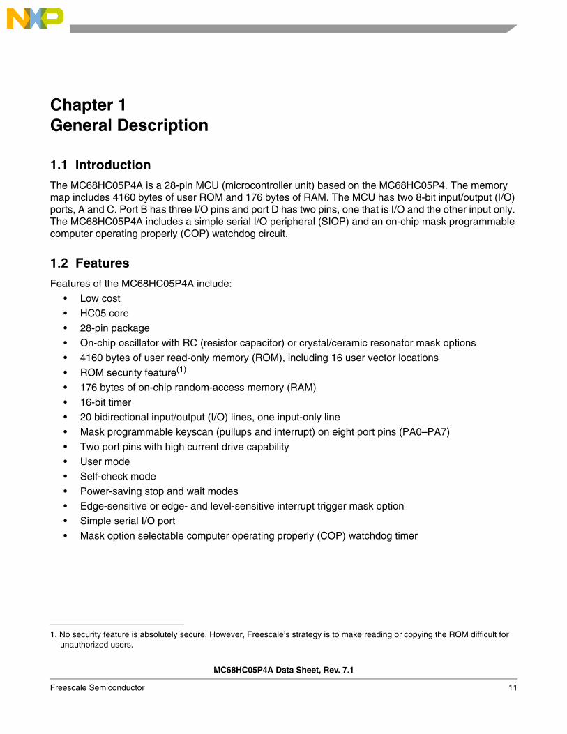
Chapter 1 General Description
1.1 Introduction
The MC68HC05P4A is a 28-pin MCU (microcontroller unit) based on the MC68HC05P4. The memory map includes 4160 bytes of user ROM and 176 bytes of RAM. The MCU has two 8-bit input/output (I/O) ports, A and C. Port B has three I/O pins and port D has two pins, one that is I/O and the other input only. The MC68HC05P4A includes a simple serial I/O peripheral (SIOP) and an on-chip mask programmable computer operating properly (COP) watchdog circuit.
1.2 Features
Features of the MC68HC05P4A include:
• Low cost
• HC05 core
• 28-pin package
• On-chip oscillator with RC (resistor capacitor) or crystal/ceramic resonator mask options
• 4160 bytes of user read-only memory (ROM), including 16 user vector locations
• ROM security feature(1)
• 176 bytes of on-chip random-access memory (RAM)
• 16-bit timer
• 20 bidirectional input/output (I/O) lines, one input-only line
• Mask programmable keyscan (pullups and interrupt) on eight port pins (PA0–PA7)
• Two port pins with high current drive capability
• User mode
• Self-check mode
• Power-saving stop and wait modes
• Edge-sensitive or edge- and level-sensitive interrupt trigger mask option
• Simple serial I/O port
• Mask option selectable computer operating properly (COP) watchdog timer
1. No security feature is absolutely secure. However, Freescale’s strategy is to make reading or copying the ROM difficult for unauthorized users.
General Description
MC68HC05P4A Data Sheet, Rev. 7.1
12 Freescale Semiconductor
1.3 Mask Options
The MC68HC05P4A has 13 mask options:
• CLOCK, RC or crystal
• IRQ, edge-sensitive only or edge- and level-sensitive
• SIOP, most significant bit (MSB) or least significant bit (LSB) first
• COP watchdog timer, enable/disable
• Keyscan pullups and interrupts on port A, enable/disable by pin
• STOP instruction
All mask options and the user ROM are programmed on the 01 layer in fabrication.
NOTENegative true signals like RESET and IRQ will be denoted with an overline.
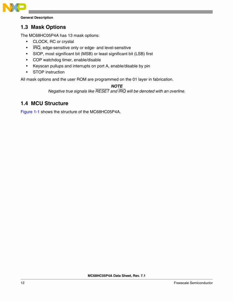
1.4 MCU Structure
Figure 1-1 shows the structure of the MC68HC05P4A.
MCU Structure
MC68HC05P4A Data Sheet, Rev. 7.1
Freescale Semiconductor 13
Figure 1-1. Block Diagram
SDO/PB5
SDI/PB6
SCK/PB7
ACCUMULATOR
INDEX REGISTER
CONDITION CODE
REGISTER
STACK POINTER
PROGRAM COUNTER
HIGH
PROGRAM COUNTER
LOW
CPU CONTROL
ALU
CPU
OSCILLATOR AND DIVIDE
BY ³ 2
DATA DIR REG
PORT B I/O LINES
INTERNAL PROCESSOR
CLOCK
RESET
IRQ
OSC1 OSC2
TIMER SYSTEM
COP SYSTEM
176 X 8RAM
240 X 8SELF-CHECK
ROM
PA0
PA1
PA2
PA3
PA4
PA5
PA6
PA7
DATA DIR REG
PORT A REG
PORT AI/O LINES
PC0
PC1
PC2
PC3
PC4
PC5
PC6
PC7
DATA DIR REG
PORT C REG
PORT C I/O LINES
PD5
TCMP
DATA DIR REG
PORT D REGPORT D
I/O LINES
TCAP/PD7
PORT B REG
4160 X 8USER ROM
General Description
MC68HC05P4A Data Sheet, Rev. 7.1
14 Freescale Semiconductor
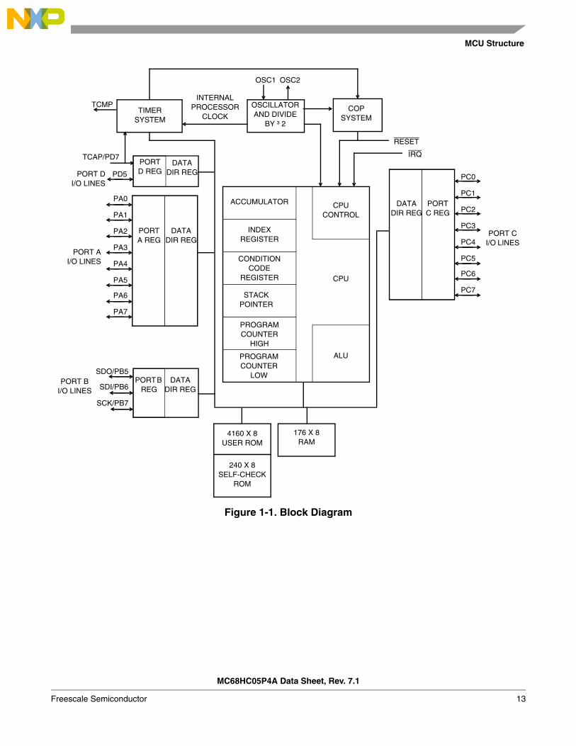
1.5 Pin Assignments
The MC68HC05P4A pin assignments are shown in Figure 1-2.
Figure 1-2. Pin Assignments
1.6 Signal Description
The following paragraphs provide a description of the signals.
1.6.1 VDD and VSS
Power is supplied to the microcontroller through VDD and VSS. VDD is the power supply and VSS is ground.
1.6.2 IRQ
This pin has a mask option that provides two different choices of interrupt triggering sensitivity. The IRQ pin contains an internal Schmitt trigger as part of its input to improve noise immunity. Refer to Chapter 3 Central Processor Unit (CPU) for more detail.
1.6.3 OSC1 and OSC2
These pins provide control input for an on-chip clock oscillator circuit. A crystal, a ceramic resonator, a resistor/capacitor combination, or an external signal connects to these pins and provides a system clock. A mask option selects either a crystal/ceramic resonator or a resistor/capacitor as the frequency determining element. The oscillator frequency is two times the internal bus rate.
1
2
3
4
5
6
7
8
9
10
11
12
13
14
27
28 VDD
OSC1
OSC2
TCAP/PD7
TCMP
PD5PC0
PC1
RESET
IRQ
PA7
PA5
PA4
PA3
PA2
PA1
PA0
PA6
15
16
17
18
19
20
SDO/PB5
SDI/PB6
SCK/PB7
VSS
21
22
23
24
25
26
PC2
PC3
PC4
PC5
PC6
PC7
Signal Description
MC68HC05P4A Data Sheet, Rev. 7.1
Freescale Semiconductor 15
1.6.4 RESET
This active low pin is used to reset the MCU to a known startup state by pulling RESET low. The RESET pin contains an internal Schmitt trigger as part of its input to improve noise immunity.
1.6.5 TCMP
This pin provides an output for the output compare feature of the on-chip timer system.
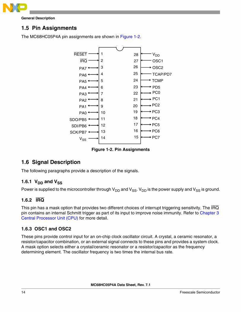
1.6.6 PA0–PA7
Port A is an 8-bit bidirectional port which does not share any of its pins with other subsystems. The port A data register is at $0000, and the data direction register is at $0004. Reset does not affect the data registers, but clears the data direction registers, thereby returning the ports to inputs. Writing a 1 to a data direction register (DDR) bit sets the corresponding port bit to output mode. Port A has mask option enabled pullup devices and interrupt capability by pin. For a detailed description of I/O programming, refer to 1.7 Input/Output Programming.
Figure 1-3. Port A Pullup Option
1.6.7 SDO/PB5, SDI/PB6, and SCK/PB7
Port B is a 3-bit bidirectional port. These pins are shared with the SIOP subsystem. Refer to Chapter 7 Simple Serial Input/Output Port (SIOP) for a detailed description of the SIOP. The address of the port B data register is $0001, and the data direction register is at address $0005. Reset does not affect the data registers, but clears the data direction registers, thereby returning the ports to inputs. Writing a 1 to a DDR bit sets the corresponding port bit to output mode.
1.6.8 PC0–PC7
Port C is an 8-bit bidirectional port which does not share any of its pins with other subsystems. The address of the port C data register is $0002, and the DDR is at address $0006. Reset does not affect the data registers, but clears the data direction registers, thereby returning the ports to inputs. Writing a 1 to a DDR bit sets the corresponding port bit to output mode. Two of the port C pins, PC0 and PC1, have a higher current drive capability. See Chapter 12 Electrical Specifications.
PA0
VDD VDD
DDR BIT
NORMAL PORT
FROM ALL OTHER PORT A PINS
IRQSCHMITTTRIGGER
TO INTERRUPTLOGIC
MASK OPTION
CIRCUITRY
General Description
MC68HC05P4A Data Sheet, Rev. 7.1
16 Freescale Semiconductor
1.6.9 PD5 and TCAP/PD7
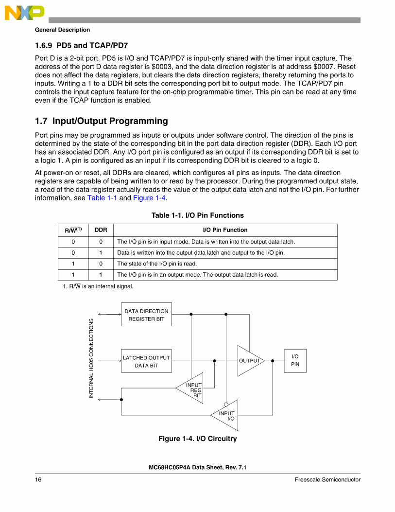
Port D is a 2-bit port. PD5 is I/O and TCAP/PD7 is input-only shared with the timer input capture. The address of the port D data register is $0003, and the data direction register is at address $0007. Reset does not affect the data registers, but clears the data direction registers, thereby returning the ports to inputs. Writing a 1 to a DDR bit sets the corresponding port bit to output mode. The TCAP/PD7 pin controls the input capture feature for the on-chip programmable timer. This pin can be read at any time even if the TCAP function is enabled.
1.7 Input/Output Programming
Port pins may be programmed as inputs or outputs under software control. The direction of the pins is determined by the state of the corresponding bit in the port data direction register (DDR). Each I/O port has an associated DDR. Any I/O port pin is configured as an output if its corresponding DDR bit is set to a logic 1. A pin is configured as an input if its corresponding DDR bit is cleared to a logic 0.
At power-on or reset, all DDRs are cleared, which configures all pins as inputs. The data direction registers are capable of being written to or read by the processor. During the programmed output state, a read of the data register actually reads the value of the output data latch and not the I/O pin. For further information, see Table 1-1 and Figure 1-4.
Figure 1-4. I/O Circuitry
Table 1-1. I/O Pin Functions
R/W(1)
1. R/W is an internal signal.
DDR I/O Pin Function
0 0 The I/O pin is in input mode. Data is written into the output data latch.
0 1 Data is written into the output data latch and output to the I/O pin.
1 0 The state of the I/O pin is read.
1 1 The I/O pin is in an output mode. The output data latch is read.
DATA DIRECTION
REGISTER BIT
LATCHED OUTPUT
DATA BIT
I/O
PIN
INPUTREG
BIT
INPUTI/O
OUTPUT
INT
ER
NA
L H
C05
CO
NN
EC
TIO
NS
MC68HC05P4A Data Sheet, Rev. 7.1
Freescale Semiconductor 17
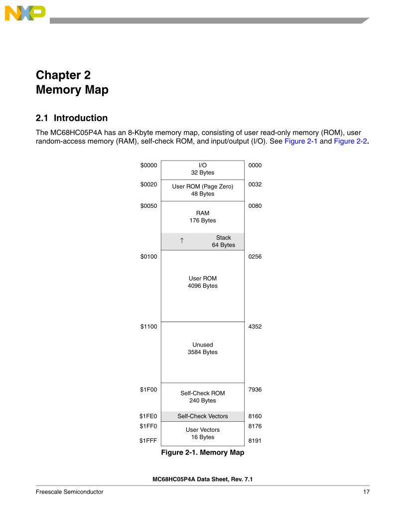
Chapter 2 Memory Map
2.1 Introduction
The MC68HC05P4A has an 8-Kbyte memory map, consisting of user read-only memory (ROM), user random-access memory (RAM), self-check ROM, and input/output (I/O). See Figure 2-1 and Figure 2-2.
$0000 I/O32 Bytes
0000
$0020 User ROM (Page Zero)48 Bytes
0032
$0050RAM
176 Bytes
0080
↑ Stack64 Bytes
$0100
User ROM4096 Bytes
0256
$1100
Unused3584 Bytes
4352
$1F00Self-Check ROM
240 Bytes
7936
$1FE0 Self-Check Vectors 8160
$1FF0
$1FFF
User Vectors16 Bytes
8176
8191
Figure 2-1. Memory Map
Memory Map
MC68HC05P4A Data Sheet, Rev. 7.1
18 Freescale Semiconductor
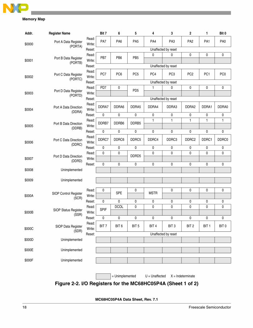
Addr. Register Name Bit 7 6 5 4 3 2 1 Bit 0
$0000Port A Data Register
(PORTA)
Read:PA7 PA6 PA5 PA4 PA3 PA2 PA1 PA0
Write:
Reset: Unaffected by reset
$0001Port B Data Register
(PORTB)
Read:PB7 PB6 PB5
0 0 0 0 0
Write:
Reset: Unaffected by reset
$0002Port C Data Register
(PORTC)
Read:PC7 PC6 PC5 PC4 PC3 PC2 PC1 PC0
Write:
Reset: Unaffected by reset
$0003Port D Data Register
(PORTD)
Read: PD7 0PD5
1 0 0 0 0
Write:
Reset: Unaffected by reset
$0004Port A Data Direction
(DDRA)
Read:DDRA7 DDRA6 DDRA5 DDRA4 DDRA3 DDRA2 DDRA1 DDRA0
Write:
Reset: 0 0 0 0 0 0 0 0
$0005Port B Data Direction
(DDRB)
Read:DDRB7 DDRB6 DDRB5
1 1 1 1 1
Write:
Reset: 0 0 0 0 0 0 0 0
$0006Port C Data Direction
(DDRC)
Read:DDRC7 DDRC6 DDRC5 DDRC4 DDRC3 DDRC2 DDRC1 DDRC0
Write:Reset: 0 0 0 0 0 0 0 0
$0007Port D Data Direction
(DDRD)
Read: 0 0DDRD5
0 0 0 0 0
Write:
Reset: 0 0 0 0 0 0 0 0
$0008 Unimplemented
$0009 Unimplemented
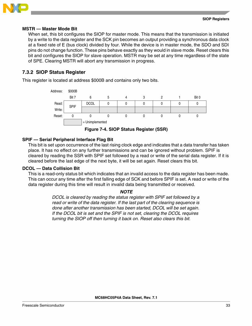
$000ASIOP Control Register
(SCR)
Read: 0SPE
0MSTR
0 0 0 0
Write:
Reset: 0 0 0 0 0 0 0 0
$000BSIOP Status Register
(SSR)
Read:SPIF
DCOL 0 0 0 0 0 0
Write:
Reset: 0 0 0 0 0 0 0 0
$000CSIOP Data Register
(SDR)
Read:BIT 7 BIT 6 BIT 5 BIT 4 BIT 3 BIT 2 BIT 1 BIT 0
Write:
Reset: Unaffected by reset
$000D Unimplemented
$000E Unimplemented
$000F Unimplemented
= Unimplemented U = Unaffected X = Indeterminate
Figure 2-2. I/O Registers for the MC68HC05P4A (Sheet 1 of 2)
Introduction
MC68HC05P4A Data Sheet, Rev. 7.1
Freescale Semiconductor 19
$0010 Unimplemented
$0011 Unimplemented
$0012Timer Control Register
(TCR)
Read:ICIE OCIE TOIE
0 0 0IEDG OLVL
Write:
Reset: 0 0 0 0 0 0 0 0
$0013Timer Status Register
(TSR)
Read: ICF OCF TOF 0 0 0 0 0
Write:
Reset: U U U 0 0 0 0 0
$0014Input Capture MSB
(ICRH)
Read: ICRH7 ICRH6 ICRH5 ICRH4 ICRH3 ICRH2 ICRH1 ICRH0
Write:
Reset: Unaffected by reset
$0015Input Capture LSB
(ICRL)
Read: ICRL7 ICRL6 ICRL5 ICRL4 ICRL3 ICRL2 ICRL1 ICRL0
Write:
Reset: Unaffected by reset
$0016Output Compare MSB
(OCRH)
Read: OCRH7 OCRH6 OCRH5 OCRH4 OCRH3 OCRH2 OCRH1 OCRH0
Write:
Reset: Unaffected by reset
$0017Output Compare LSB
(OCRL)
Read: OCRL7 OCRL6 OCRL5 OCRL4 OCRL3 OCRL2 OCRL1 OCRL0
Write:
Reset: Unaffected by reset
$0018Counter MSB
(CRH)
Read: CRH7 CRH6 CRH5 CRH4 CRH3 CRH2 CRH1 CRH0
Write:
Reset: Unaffected by reset
$0019Counter LSB
(CRL)
Read: CRL7 CRL6 CRL5 CRL4 CRL3 CRL2 CRL1 CRL0
Write:
Reset: Unaffected by reset
$001ADual Timer MSB (DTMH)
Counter Alternate Register
Read: DTMH7 DTMH6 DTMH5 DTMH4 DTMH3 DTMH2 DTMH1 DTMH0
Write:
Reset: Unaffected by reset
$001BDual Timer LSB (DTML)
Counter Alternate Register
Read: DTML7 DTML6 DTML5 DTML4 DTML3 DTML2 DTML1 DTML0
Write:
Reset: Unaffected by reset
$001C Unimplemented
$001D Unimplemented
$001E Unimplemented
$001F Reserved R R R R R R R R
Addr. Register Name Bit 7 6 5 4 3 2 1 Bit 0
= Unimplemented U = Unaffected X = Indeterminate
Figure 2-2. I/O Registers for the MC68HC05P4A (Sheet 2 of 2)
Memory Map
MC68HC05P4A Data Sheet, Rev. 7.1
20 Freescale Semiconductor
2.2 ROM
The user ROM consists of 48 bytes of page zero ROM from $0020 to $004F, 4096 bytes of ROM from $0100 to $10FF, and 16 bytes of user vectors from $1FF0 to $1FFF. The self-check ROM and vectors are located from $1F00 to $1FEF.
2.3 ROM Security Feature
A security feature(1) has been incorporated into the MC68HC05P4A to help prevent external reading of code in the ROM. Placing unique customer code at ROM locations $0028–$002F aids in keeping customer developed software proprietary.
2.4 RAM
The user RAM consists of 176 bytes of a shared stack area. The stack begins at address $00FF. The stack pointer can access 64 bytes of RAM in the range $00FF to $00C0.
NOTEUsing the stack area for data storage or temporary work locations requires care to prevent it from being overwritten due to stacking from an interrupt or subroutine call.
1. No security feature is absolutely secure. However, Freescale’s strategy is to make reading or copying the ROM difficult for unauthorized users.
MC68HC05P4A Data Sheet, Rev. 7.1
Freescale Semiconductor 21
Chapter 3 Central Processor Unit (CPU)
3.1 Introduction
This section describes the five CPU registers. CPU registers are not part of the memory map.
3.2 Accumulator (A)
The accumulator is a general-purpose 8-bit register used to hold operands and results of arithmetic calculations or data manipulations.
3.3 Index Register (X)
The index register is an 8-bit register used for the indexed addressing value to create an effective address. The index register also may be used as a temporary storage area.
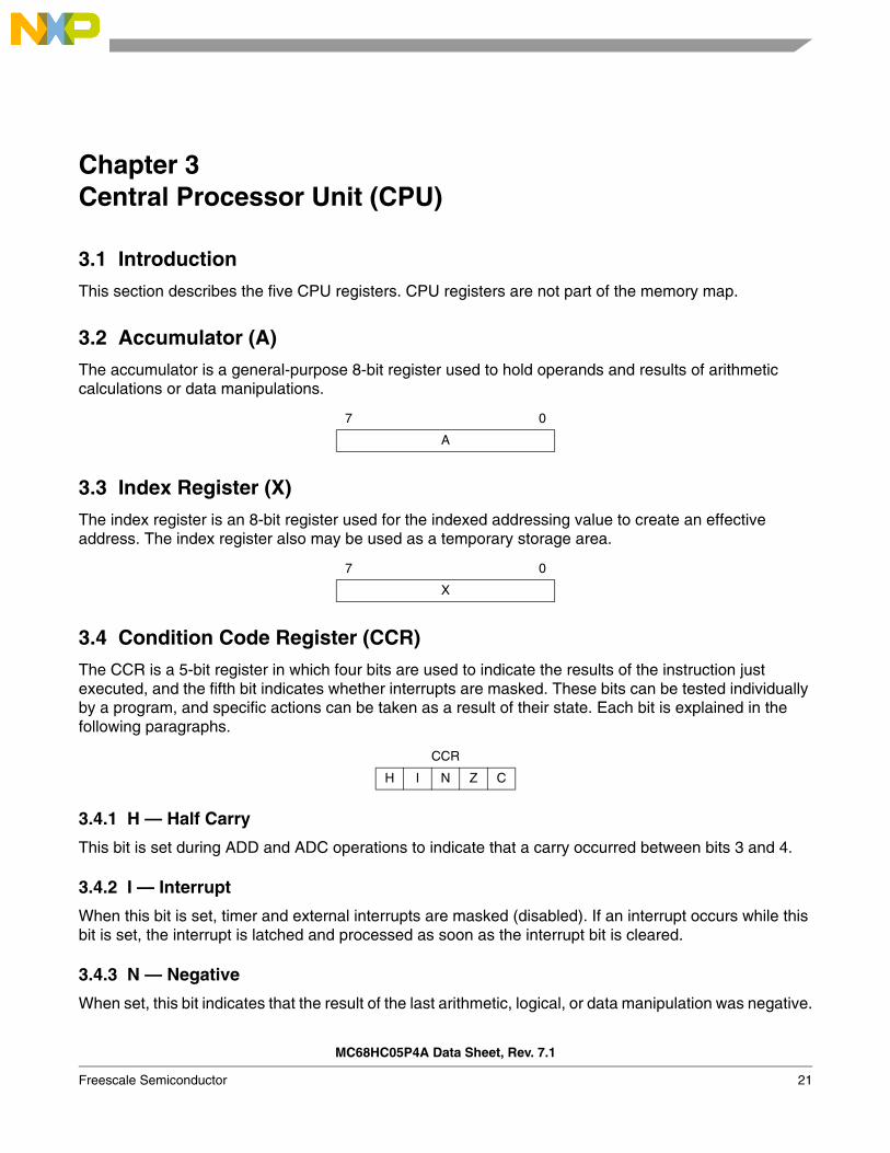
3.4 Condition Code Register (CCR)
The CCR is a 5-bit register in which four bits are used to indicate the results of the instruction just executed, and the fifth bit indicates whether interrupts are masked. These bits can be tested individually by a program, and specific actions can be taken as a result of their state. Each bit is explained in the following paragraphs.
3.4.1 H — Half Carry
This bit is set during ADD and ADC operations to indicate that a carry occurred between bits 3 and 4.
3.4.2 I — Interrupt
When this bit is set, timer and external interrupts are masked (disabled). If an interrupt occurs while this bit is set, the interrupt is latched and processed as soon as the interrupt bit is cleared.
3.4.3 N — Negative
When set, this bit indicates that the result of the last arithmetic, logical, or data manipulation was negative.
7 0
A
7 0
X
CCR
H I N Z C
Central Processor Unit (CPU)
MC68HC05P4A Data Sheet, Rev. 7.1
22 Freescale Semiconductor
3.4.4 Z — Zero
When set, this bit indicates that the result of the last arithmetic, logical, or data manipulation was 0.
3.4.5 C — Carry/Borrow
When set, this bit indicates that a carry or borrow out of the arithmetic logical unit (ALU) occurred during the last arithmetic operation. This bit is also affected during bit test and branch instructions and during shifts and rotates.
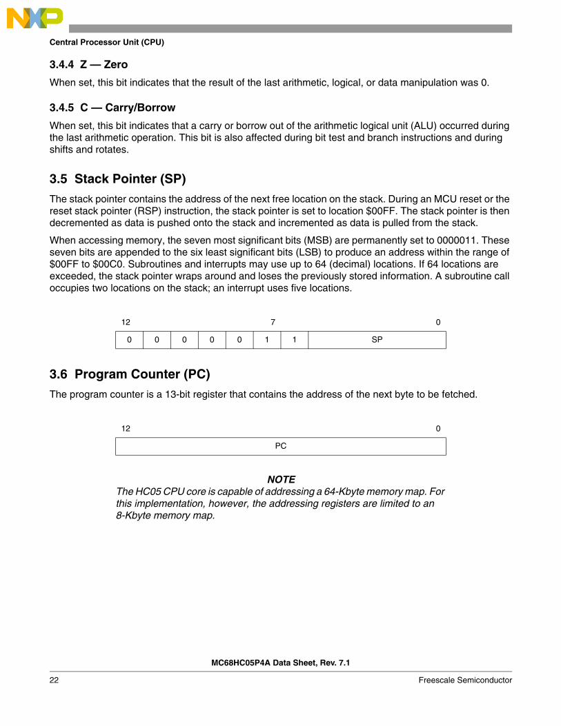
3.5 Stack Pointer (SP)
The stack pointer contains the address of the next free location on the stack. During an MCU reset or the reset stack pointer (RSP) instruction, the stack pointer is set to location $00FF. The stack pointer is then decremented as data is pushed onto the stack and incremented as data is pulled from the stack.
When accessing memory, the seven most significant bits (MSB) are permanently set to 0000011. These seven bits are appended to the six least significant bits (LSB) to produce an address within the range of $00FF to $00C0. Subroutines and interrupts may use up to 64 (decimal) locations. If 64 locations are exceeded, the stack pointer wraps around and loses the previously stored information. A subroutine call occupies two locations on the stack; an interrupt uses five locations.
3.6 Program Counter (PC)
The program counter is a 13-bit register that contains the address of the next byte to be fetched.
NOTEThe HC05 CPU core is capable of addressing a 64-Kbyte memory map. For this implementation, however, the addressing registers are limited to an 8-Kbyte memory map.
12 7 0
0 0 0 0 0 1 1 SP
12 0
PC
MC68HC05P4A Data Sheet, Rev. 7.1
Freescale Semiconductor 23
Chapter 4 Interrupts
4.1 Introduction
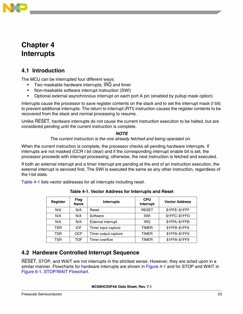
The MCU can be interrupted four different ways: • Two maskable hardware interrupts, IRQ and timer • Non-maskable software interrupt instruction (SWI) • Optional external asynchronous interrupt on each port A pin (enabled by pullup mask option)
Interrupts cause the processor to save register contents on the stack and to set the interrupt mask (I bit) to prevent additional interrupts. The return to interrupt (RTI) instruction causes the register contents to be recovered from the stack and normal processing to resume.
Unlike RESET, hardware interrupts do not cause the current instruction execution to be halted, but are considered pending until the current instruction is complete.
NOTEThe current instruction is the one already fetched and being operated on.
When the current instruction is complete, the processor checks all pending hardware interrupts. If interrupts are not masked (CCR I bit clear) and if the corresponding interrupt enable bit is set, the processor proceeds with interrupt processing; otherwise, the next instruction is fetched and executed.
If both an external interrupt and a timer interrupt are pending at the end of an instruction execution, the external interrupt is serviced first. The SWI is executed the same as any other instruction, regardless of the I-bit state.
Table 4-1 lists vector addresses for all interrupts including reset.
4.2 Hardware Controlled Interrupt Sequence
RESET, STOP, and WAIT are not interrupts in the strictest sense. However, they are acted upon in a similar manner. Flowcharts for hardware interrupts are shown in Figure 4-1 and for STOP and WAIT in Figure 6-1. STOP/WAIT Flowchart.
Table 4-1. Vector Address for Interrupts and Reset
RegisterFlag
NameInterrupts
CPUInterrupt
Vector Address
N/A N/A Reset RESET $1FFE–$1FFF
N/A N/A Software SWI $1FFC–$1FFD
N/A N/A External interrupt IRQ $1FFA–$1FFB
TSR ICF Timer input capture TIMER $1FF8–$1FF9
TSR OCF Timer output capture TIMER $1FF8–$1FF9
TSR TOF Timer overflow TIMER $1FF8–$1FF9
Interrupts
MC68HC05P4A Data Sheet, Rev. 7.1
24 Freescale Semiconductor
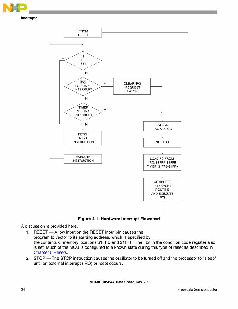
Figure 4-1. Hardware Interrupt Flowchart
A discussion is provided here.1. RESET — A low input on the RESET input pin causes the
program to vector to its starting address, which is specified bythe contents of memory locations $1FFE and $1FFF. The I bit in the condition code register also is set. Much of the MCU is configured to a known state during this type of reset as described in Chapter 5 Resets.
2. STOP — The STOP instruction causes the oscillator to be turned off and the processor to "sleep" until an external interrupt (IRQ) or reset occurs.
FROMRESET
EXTERNALINTERRUPT
IRQ
INTERNAL INTERRUPT
TIMER
I BIT SET
IS
LOAD PC FROM:IRQ: $1FFA–$1FFB
TIMER: $1FF8–$1FF9
SET I BIT
STACKPC, X, A, CC
CLEAR IRQ REQUEST
LATCH
COMPLETEINTERRUPT
ROUTINEAND EXECUTE
RTI
FETCH NEXT
INSTRUCTION
EXECUTEINSTRUCTION
Y
Y
Y
N
N
N
Timer Interrupt
MC68HC05P4A Data Sheet, Rev. 7.1
Freescale Semiconductor 25
3. WAIT or HALT — The WAIT or HALT instruction causes all processor clocks to stop, but leaves the timer clock running. This rest state of the processor can be cleared by reset, an external interrupt (IRQ), or timer interrupt. These individual interrupts have no special wait vectors. See 6.3 WAIT Instruction.
4.3 Timer Interrupt
Three different timer interrupt flags cause a timer interrupt when they are set and enabled. The interrupt flags are in the timer status register (TSR), and the enable bits are in the timer control register (TCR). Any of these interrupts will vector to the same interrupt service routine, located at the address specified by the contents of memory locations $1FF8 and $1FF9.
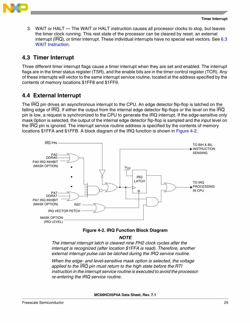
4.4 External Interrupt
The IRQ pin drives an asynchronous interrupt to the CPU. An edge detector flip-flop is latched on the falling edge of IRQ. If either the output from the internal edge detector flip-flops or the level on the IRQ pin is low, a request is synchronized to the CPU to generate the IRQ interrupt. If the edge-sensitive only mask 0ption is selected, the output of the internal edge detector flip-flop is sampled and the input level on the IRQ pin is ignored. The interrupt service routine address is specified by the contents of memory locations $1FFA and $1FFB. A block diagram of the IRQ function is shown in Figure 4-2.
Figure 4-2. IRQ Function Block Diagram
NOTEThe internal interrupt latch is cleared nine PH2 clock cycles after the interrupt is recognized (after location $1FFA is read). Therefore, another external interrupt pulse can be latched during the IRQ service routine.
When the edge- and level-sensitive mask option is selected, the voltage applied to the IRQ pin must return to the high state before the RTI instruction in the interrupt service routine is executed to avoid the processor re-entering the IRQ service routine.
IRQLATCH
R
VDD
IRQ PIN
MASK OPTION(IRQ LEVEL)
TO IRQ PROCESSING IN CPU
TO BIH & BILINSTRUCTION SENSING
RST
IRQ VECTOR FETCH
PA7DDRA7
PA0DDRA0
PA0 IRQ INHIBIT(MASK OPTION)
PA7 IRQ INHIBIT(MASK OPTION)
Interrupts
MC68HC05P4A Data Sheet, Rev. 7.1
26 Freescale Semiconductor
The IRQ pin is one source of an IRQ interrupt and a mask option can also enable the port A pins (PA0–PA7) to act as other IRQ interrupt sources. These sources are all combined into a single ORing function to be latched by the IRQ latch.
Any enabled IRQ interrupt source sets the IRQ latch on the falling edge of the IRQ pin or a port A pin if port A interrupts have been enabled. If edge-only sensitivity is chosen by a mask option, only the IRQ latch output can activate a request to the CPU to generate the IRQ interrupt sequence. This makes the IRQ interrupt sensitive to:
1. Falling edge on the IRQ pin with all enabled port A interrupt pins at a high level2. Falling edge on any enabled port A interrupt pin with all other enabled port A interrupt pins and the
IRQ pin at a high level
If level sensitivity is chosen, the active high state of the IRQ input can also activate an IRQ request to the CPU to generate the IRQ interrupt sequence. This makes the IRQ interrupt sensitive to:
1. Low level on the IRQ pin2. Falling edge on the IRQ pin with all enabled port A interrupt pins at a high level3. Low level on any enabled port A interrupt pin4. Falling edge on any enabled port A interrupt pin with all enabled port A interrupt pins on the IRQ
pin at a high level
This interrupt is serviced by the interrupt service routine located at the address specified by the contents of $1FFA and $1FFB. The IRQ latch is automatically cleared by entering the interrupt service routine.
4.5 Optional External Interrupts (PA0–PA7)
The IRQ interrupt can be triggered by the inputs on the PA0–PA7 port pins if enabled by individual mask options. With pullup enabled, each port A pin can activate the IRQ interrupt function and the interrupt operation will be the same as for inputs to the IRQ pin. Once enabled by mask option, each individual port A pin can be disabled as an interrupt source if its corresponding DDR bit is configured for output mode.
NOTEThe BIH and BIL instructions apply to the output of the logic OR function of the enabled PA0–PA7 interrupt pins and the IRQ pin. The BIH and BIL instructions do not exclusively test the state of the IRQ pin.
If enabled, the PA0–PA7 pins will cause an IRQ interrupt only if these individual pins are configured as inputs.
4.6 Software Interrupt (SWI)
The SWI is an executable instruction and a non-maskable interrupt. It is executed regardless of the state of the I bit in the CCR. If the I bit is 0 (interrupts enabled), SWI executes after interrupts which were pending when the SWI was fetched but before interrupts generated after the SWI was fetched. The interrupt service routine address is specified by the contents of memory locations $1FFC and $1FFD.
MC68HC05P4A Data Sheet, Rev. 7.1
Freescale Semiconductor 27
Chapter 5 Resets
5.1 Introduction
The MCU can be reset three ways: 1. Initial power-on reset function2. Active low input to the RESET pin3. Computer operating properly (COP) watchdog timer timeout
5.2 Power-On Reset (POR)
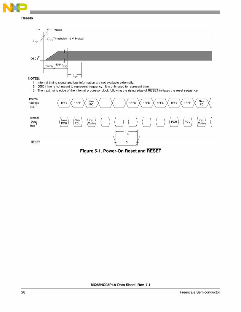
An internal reset is generated on power-up to allow the internal clock generator to stabilize. The power-on reset is strictly for power turn-on conditions and should not be used to detect a drop in the power supply voltage.
There is a 4064 internal processor clock cycle (tcyc) oscillator stabilization delay after the oscillator becomes active. If the RESET pin is low at the end of this 4064-cycle delay, the MCU will remain in the reset condition until RESET goes high.
5.3 RESET Pin
The MCU is reset when a logic 0 is applied to the RESET input for a period of one and one-half machine cycles (tcyc).
5.4 Computer Operating Properly (COP) Reset
The MCU contains a watchdog timer that automatically times out if not reset (cleared) within a specific time by a program reset sequence. If the COP watchdog timer is allowed to time out, an internal reset is generated to reset the MCU. Because the internal RESET signal is used, the MCU comes out of a COP reset in the same operating mode it was in when the COP timeout was generated.
The COP reset function is enabled or disabled by a mask option.
Refer to Chapter 9 Computer Operating Properly (COP) for more information on the COP.
Resets
MC68HC05P4A Data Sheet, Rev. 7.1
28 Freescale Semiconductor
Figure 5-1. Power-On Reset and RESET
OSC12
RESET
InternalClock 1
InternalAddressBus 1
1FFE 1FFF New
New New Op PCHPCL
VDDVDD Threshold (1-2 V Typical)
tVDDR
tOXOV 4064 tcyc
tcyc
tRL
InternalDataBus 1
1FFE1FFE1FFE 1FFE New1FFF
PCH PCL OpCodeCodePCLPCH
NOTES:1. Internal timing signal and bus information are not available externally.2. OSC1 line is not meant to represent frequency. It is only used to represent time.3. The next rising edge of the internal processor clock following the rising edge of RESET initiates the reset sequence.
3
PCPC
MC68HC05P4A Data Sheet, Rev. 7.1
Freescale Semiconductor 29
Chapter 6 Low-Power Modes
6.1 Introduction
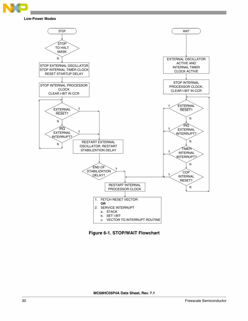
The MC68HC05P4A is capable of running in a low-power mode in each of its configurations. The WAIT and STOP instructions provide two modes that reduce the power required for the MCU by stopping various internal clocks and/or the on-chip oscillator. The STOP and WAIT instructions are not normally used if the computer operating properly (COP) watchdog timer is enabled. The flow of the stop and wait modes is shown in Figure 6-1.
6.2 Stop Mode
Execution of the STOP instruction places the MCU in its lowest power consumption mode. In stop mode, the internal oscillator is turned off, halting all internal processing, including the COP watchdog timer. Execution of the STOP instruction automatically clears the I bit in the condition code register so that the IRQ external interrupt is enabled. All other registers and memory remain unaltered. All input/output lines remain unchanged.
The MCU can be brought out of stop mode only by an IRQ external interrupt or an externally generated RESET. When exiting the stop mode, the internal oscillator will resume after a 4064 PH2 clock cycle oscillator stabilization delay.
6.3 WAIT Instruction
The WAIT instruction places the MCU in a low-power mode, which consumes more power than stop mode. In wait mode, the PH2 clock is halted, suspending all processor and internal bus activity. Internal timer clocks remain active, permitting interrupts to be generated from the 16-bit timer and reset to be generated from the COP watchdog timer. Execution of the WAIT instruction automatically clears the I bit in the condition code register enabling the IRQ external interrupt. All other registers, memory, and input/output lines remain in their previous state.
If the 16-bit timer interrupt is enabled, it will cause the processor to exit wait mode and resume normal operation. The 16-bit timer may be used to generate a periodic exit from wait mode. The wait mode may also be exited when an IRQ external interrupt or RESET occurs.
Low-Power Modes
MC68HC05P4A Data Sheet, Rev. 7.1
30 Freescale Semiconductor
Figure 6-1. STOP/WAIT Flowchart
1. FETCH RESET VECTOROR
2. SERVICE INTERRUPTa. STACKb. SET I BITc. VECTOR TO INTERRUPT ROUTINE
WAIT
STOPTO HALT
MASK
N
EXTERNALRESET?
Y
N
IRQEXTERNAL
INTERRUPT?
Y
N
STOP EXTERNAL OSCILLATORSTOP INTERNAL TIMER CLOCK
RESET STARTUP DELAY
RESTART EXTERNALOSCILLATOR, RESTARTSTABILIZATION DELAY
STOP INTERNAL PROCESSOR CLOCK
CLEAR I-BIT IN CCR
END OFSTABILIZATION
DELAY?
Y
IRQEXTERNAL
INTERRUPT?
Y
N
EXTERNAL OSCILLATORACTIVE AND
INTERNAL TIMERCLOCK ACTIVE
RESTART INTERNALPROCESSOR CLOCK
STOP INTERNALPROCESSOR CLOCK,CLEAR I-BIT IN CCR
TIMERINTERNAL
INTERRUPT?
Y
N
EXTERNALRESET?
Y
N
STOP
COPINTERNALRESET?
Y
N
MC68HC05P4A Data Sheet, Rev. 7.1
Freescale Semiconductor 31
Chapter 7 Simple Serial Input/Output Port (SIOP)
7.1 Introduction
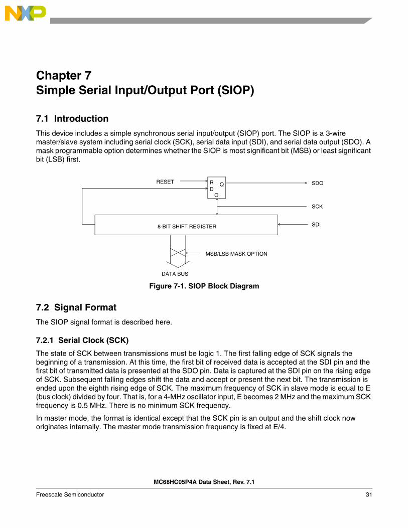
This device includes a simple synchronous serial input/output (SIOP) port. The SIOP is a 3-wire master/slave system including serial clock (SCK), serial data input (SDI), and serial data output (SDO). A mask programmable option determines whether the SIOP is most significant bit (MSB) or least significant bit (LSB) first.
Figure 7-1. SIOP Block Diagram
7.2 Signal Format
The SIOP signal format is described here.
7.2.1 Serial Clock (SCK)
The state of SCK between transmissions must be logic 1. The first falling edge of SCK signals the beginning of a transmission. At this time, the first bit of received data is accepted at the SDI pin and the first bit of transmitted data is presented at the SDO pin. Data is captured at the SDI pin on the rising edge of SCK. Subsequent falling edges shift the data and accept or present the next bit. The transmission is ended upon the eighth rising edge of SCK. The maximum frequency of SCK in slave mode is equal to E (bus clock) divided by four. That is, for a 4-MHz oscillator input, E becomes 2 MHz and the maximum SCK frequency is 0.5 MHz. There is no minimum SCK frequency.
In master mode, the format is identical except that the SCK pin is an output and the shift clock now originates internally. The master mode transmission frequency is fixed at E/4.
8-BIT SHIFT REGISTER
DQR
C
RESET SDO
SCK
SDI
MSB/LSB MASK OPTION
DATA BUS
Simple Serial Input/Output Port (SIOP)
MC68HC05P4A Data Sheet, Rev. 7.1
32 Freescale Semiconductor
7.2.2 Serial Data Out (SDO)
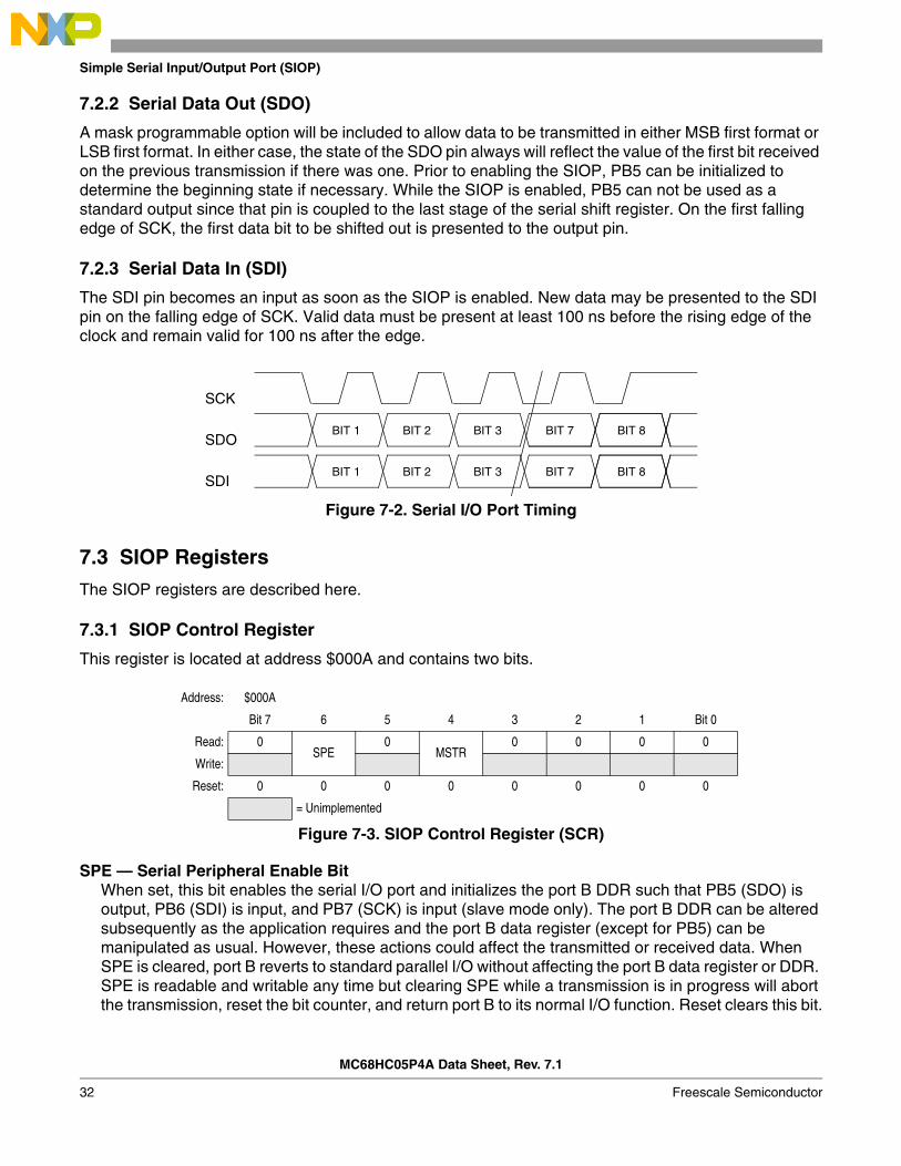
A mask programmable option will be included to allow data to be transmitted in either MSB first format or LSB first format. In either case, the state of the SDO pin always will reflect the value of the first bit received on the previous transmission if there was one. Prior to enabling the SIOP, PB5 can be initialized to determine the beginning state if necessary. While the SIOP is enabled, PB5 can not be used as a standard output since that pin is coupled to the last stage of the serial shift register. On the first falling edge of SCK, the first data bit to be shifted out is presented to the output pin.
7.2.3 Serial Data In (SDI)
The SDI pin becomes an input as soon as the SIOP is enabled. New data may be presented to the SDI pin on the falling edge of SCK. Valid data must be present at least 100 ns before the rising edge of the clock and remain valid for 100 ns after the edge.
Figure 7-2. Serial I/O Port Timing
7.3 SIOP Registers
The SIOP registers are described here.
7.3.1 SIOP Control Register
This register is located at address $000A and contains two bits.
SPE — Serial Peripheral Enable BitWhen set, this bit enables the serial I/O port and initializes the port B DDR such that PB5 (SDO) is output, PB6 (SDI) is input, and PB7 (SCK) is input (slave mode only). The port B DDR can be altered subsequently as the application requires and the port B data register (except for PB5) can be manipulated as usual. However, these actions could affect the transmitted or received data. When SPE is cleared, port B reverts to standard parallel I/O without affecting the port B data register or DDR. SPE is readable and writable any time but clearing SPE while a transmission is in progress will abort the transmission, reset the bit counter, and return port B to its normal I/O function. Reset clears this bit.
Address: $000A
Bit 7 6 5 4 3 2 1 Bit 0
Read: 0SPE
0MSTR
0 0 0 0
Write:
Reset: 0 0 0 0 0 0 0 0
= Unimplemented
Figure 7-3. SIOP Control Register (SCR)
SDOBIT 1 BIT 2 BIT 3 BIT 7
SCK
BIT 8
SDIBIT 1 BIT 2 BIT 3 BIT 7
BIT 8
SIOP Registers
MC68HC05P4A Data Sheet, Rev. 7.1
Freescale Semiconductor 33
MSTR — Master Mode BitWhen set, this bit configures the SIOP for master mode. This means that the transmission is initiated by a write to the data register and the SCK pin becomes an output providing a synchronous data clock at a fixed rate of E (bus clock) divided by four. While the device is in master mode, the SDO and SDI pins do not change function. These pins behave exactly as they would in slave mode. Reset clears this bit and configures the SIOP for slave operation. MSTR may be set at any time regardless of the state of SPE. Clearing MSTR will abort any transmission in progress.
7.3.2 SIOP Status Register
This register is located at address $000B and contains only two bits.
SPIF — Serial Peripheral Interface Flag BitThis bit is set upon occurrence of the last rising clock edge and indicates that a data transfer has taken place. It has no effect on any further transmissions and can be ignored without problem. SPIF is cleared by reading the SSR with SPIF set followed by a read or write of the serial data register. If it is cleared before the last edge of the next byte, it will be set again. Reset clears this bit.
DCOL — Data Collision BitThis is a read-only status bit which indicates that an invalid access to the data register has been made. This can occur any time after the first falling edge of SCK and before SPIF is set. A read or write of the data register during this time will result in invalid data being transmitted or received.
NOTEDCOL is cleared by reading the status register with SPIF set followed by a read or write of the data register. If the last part of the clearing sequence is done after another transmission has been started, DCOL will be set again. If the DCOL bit is set and the SPIF is not set, clearing the DCOL requires turning the SIOP off then turning it back on. Reset also clears this bit.
Address: $000B
Bit 7 6 5 4 3 2 1 Bit 0
Read:SPIF
DCOL 0 0 0 0 0 0
Write:
Reset: 0 0 0 0 0 0 0 0
= Unimplemented
Figure 7-4. SIOP Status Register (SSR)
Simple Serial Input/Output Port (SIOP)
MC68HC05P4A Data Sheet, Rev. 7.1
34 Freescale Semiconductor
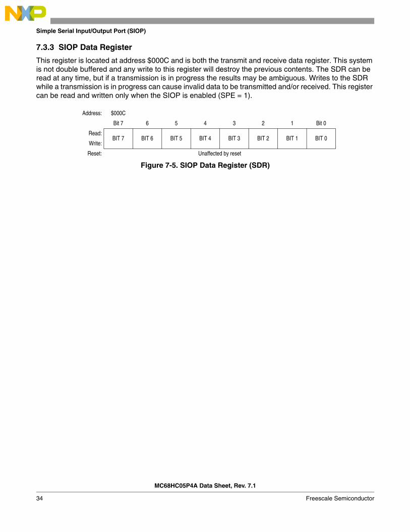
7.3.3 SIOP Data Register
This register is located at address $000C and is both the transmit and receive data register. This system is not double buffered and any write to this register will destroy the previous contents. The SDR can be read at any time, but if a transmission is in progress the results may be ambiguous. Writes to the SDR while a transmission is in progress can cause invalid data to be transmitted and/or received. This register can be read and written only when the SIOP is enabled (SPE = 1).
Address: $000C
Bit 7 6 5 4 3 2 1 Bit 0
Read:BIT 7 BIT 6 BIT 5 BIT 4 BIT 3 BIT 2 BIT 1 BIT 0
Write:
Reset: Unaffected by reset
Figure 7-5. SIOP Data Register (SDR)
MC68HC05P4A Data Sheet, Rev. 7.1
Freescale Semiconductor 35
Chapter 8 Timer
8.1 Introduction
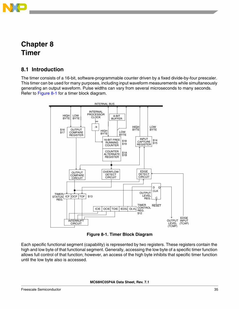
The timer consists of a 16-bit, software-programmable counter driven by a fixed divide-by-four prescaler. This timer can be used for many purposes, including input waveform measurements while simultaneously generating an output waveform. Pulse widths can vary from several microseconds to many seconds. Refer to Figure 8-1 for a timer block diagram.
Figure 8-1. Timer Block Diagram
Each specific functional segment (capability) is represented by two registers. These registers contain the high and low byte of that functional segment. Generally, accessing the low byte of a specific timer function allows full control of that function; however, an access of the high byte inhibits that specific timer function until the low byte also is accessed.
EDGEINPUT(TCAP)
INPUTCAPTUREREGISTER
CLOCK
INTERNAL BUS
OUTPUTCOMPAREREGISTER
HIGHBYTE
LOWBYTE
$16$17
³³³
/4
INTERNALPROCESSOR
16-BIT FREERUNNINGCOUNTER
COUNTERALTERNATEREGISTER
8-BITBUFFER
HIGHBYTE LOW
BYTE
$1A$1B
$18$19
HIGHBYTE
LOWBYTE
$14$15
OUTPUTCOMPARECIRCUIT
OVERFLOWDETECTCIRCUIT
EDGEDETECTCIRCUIT
TIMERSTATUS
REG.ICF OCF TOF $13
ICIE IEDG OLVL
OUTPUTLEVEL
REG.
RESETTIMERCONTROLREG.$12
OUTPUTLEVEL(TCMP)
INTERRUPTCIRCUIT
TOIEOCIE
DCLK
C
Q
Timer
MC68HC05P4A Data Sheet, Rev. 7.1
36 Freescale Semiconductor
NOTEThe I bit in the CCR should be set while manipulating both the high and low byte register of a specific timer function to ensure that an interrupt does not occur.
8.2 Counter
The key element in the programmable timer is a 16-bit, free-running counter or counter register, preceded by a prescaler that divides the internal processor clock by four. The prescaler gives the timer a resolution of 2.0 microseconds if the internal bus clock is 2.0 MHz. The counter is incremented during the low portion of the internal bus clock. Software can read the counter at any time without affecting its value.
The double-byte, free-running counter can be read from either of two locations, $18–$19 (counter register) or $1A–$1B (counter alternate register). A read from only the least significant byte (LSB) of the free-running counter ($19, $1B) receives the count value at the time of the read. If a read of the free-running counter or counter alternate register first addresses the most significant byte (MSB) ($18, $1A), the LSB ($19, $1B) is transferred to a buffer. This buffer value remains fixed after the first MSB read, even if the user reads the MSB several times. This buffer is accessed when reading the free-running counter or counter alternate register LSB ($19 or $1B) and, thus, completes a read sequence of the total counter value. In reading either the free-running counter or counter alternate register, if the MSB is read, the LSB also must be read to complete the sequence.
The counter alternate register differs from the counter register in one respect: A read of the counter register MSB can clear the timer overflow flag (TOF). Therefore, the counter alternate register can be read at any time without the possibility of missing timer overflow interrupts due to clearing of the TOF.
The free-running counter is configured to $FFFC during reset and is always a read-only register. During a power-on reset, the counter is also preset to $FFFC and begins running after the oscillator startup delay. Because the free-running counter is 16 bits preceded by a fixed divided-by-four prescaler, the value in the free-running counter repeats every 262,144 internal bus clock cycles. When the counter rolls over from $FFFF to $0000, the TOF bit is set. An interrupt can also be enabled when counter rollover occurs by setting its interrupt enable bit (TOIE).
8.3 Output Compare Register
The 16-bit output compare register is made up of two 8-bit registers at locations $16 (MSB) and $17 (LSB). The output compare register is used for several purposes, such as indicating when a period of time has elapsed. All bits are readable and writable and are not altered by the timer hardware or reset. If the compare function is not needed, the two bytes of the output compare register can be used as storage locations.
The output compare register contents are compared with the contents of the free-running counter continually, and if a match is found, the corresponding output compare flag (OCF) bit is set and the corresponding output level (OLVL) bit is clocked to an output level register. The output compare register values and the output level bit should be changed after each successful comparison to establish a new elapsed timeout. An interrupt can also accompany a successful output compare provided the corresponding interrupt enable bit (OCIE) is set.
After a processor write cycle to the output compare register containing the MSB ($16), the output compare function is inhibited until the LSB ($17) is also written. The user must write both bytes (locations) if the MSB is written first. A write made only to the LSB ($17) will not inhibit the compare function. The
Input Capture Register
MC68HC05P4A Data Sheet, Rev. 7.1
Freescale Semiconductor 37
free-running counter is updated every four internal bus clock cycles. The minimum time required to update the output compare register is a function of the program rather than the internal hardware.
The processor can write to either byte of the output compare register without affecting the other byte. The output level (OLVL) bit is clocked to the output level register regardless of whether the output compare flag (OCF) is set or clear.
8.4 Input Capture Register
Two 8-bit registers, which make up the 16-bit input capture register, are read-only and are used to latch the value of the free-running counter after the corresponding input capture edge detector senses a defined transition. The level transition which triggers the counter transfer is defined by the corresponding input edge bit (IEDG). Reset does not affect the contents of the input capture register.
The result obtained by an input capture will be one more than the value of the free-running counter on the rising edge of the internal bus clock preceding the external transition. This delay is required for internal synchronization. Resolution is one count of the free-running counter, which is four internal bus clock cycles.
The free-running counter contents are transferred to the input capture register on each proper signal transition regardless of whether the input capture flag (ICF) is set or clear. The input capture register always contains the free-running counter value that corresponds to the most recent input capture.
After a read of the input capture register ($14) MSB, the counter transfer is inhibited until the LSB ($15) is also read. This characteristic causes the time used in the input capture software routine and its interaction with the main program to determine the minimum pulse period.
A read of the input capture register LSB ($15) does not inhibit the free-running counter transfer since they occur on opposite edges of the internal bus clock.
8.5 Timer Control Register
The timer control register (TCR) is a read/write register containing five control bits. Three bits control interrupts associated with the timer status register flags ICF, OCF, and TOF.
ICIE — Input Capture Interrupt Enable Bit1 = Interrupt enabled0 = Interrupt disabled
OCIE — Output Compare Interrupt Enable Bit1 = Interrupt enabled0 = Interrupt disabled
Address: $0012
Bit 7 6 5 4 3 2 1 Bit 0
Read:ICIE OCIE TOIE
0 0 0IEDG OLVL
Write:
Reset: 0 0 0 0 0 0 0 0
= Unimplemented
Figure 8-2. Timer Control Register (TCR)
Timer
MC68HC05P4A Data Sheet, Rev. 7.1
38 Freescale Semiconductor
TOIE — Timer Overflow Interrupt Enable Bit1 = Interrupt enabled0 = Interrupt disabled
IEDG — Input Edge BitValue of input edge determines which level transition on TCAP pin will trigger free-running counter transfer to the input capture register. Reset does not affect the IEDG bit.
1 = Positive edge0 = Negative edge
OLVL — Output Level BitValue of output level is clocked into output level register by the next successful output compare and will appear on the TCMP pin.
1 = High output0 = Low output
Bits 2, 3, and 4 — Not usedAlways read 0
8.6 Timer Status Register
The timer status register (TSR) is a read-only register containing three status flag bits.
ICF — Input Capture Flag Bit1 = Flag set when selected polarity edge is sensed by input capture edge detector0 = Flag cleared when TSR and input capture low register ($15) are accessed
OCF — Output Compare Flag Bit1 = Flag set when output compare register contents match the free-running counter contents0 = Flag cleared when TSR and output compare low register ($17) are accessed
TOF — Timer Overflow Flag Bit1 = Flag set when free-running counter transition from $FFFF to $0000 occurs0 = Flag cleared when TSR and counter low register ($19) are accessed
Bits 0–4 — Not usedAlways read 0
Accessing the timer status register satisfies the first condition required to clear status bits. The remaining step is to access the register corresponding to the status bit.
Address: $0013
Bit 7 6 5 4 3 2 1 Bit 0
Read: ICF OCF TOF 0 0 0 0 0
Write:
Reset: U U U 0 0 0 0 0
= Unimplemented
Figure 8-3. Timer Status Register (TSR)
Timer During Wait or Halt Mode
MC68HC05P4A Data Sheet, Rev. 7.1
Freescale Semiconductor 39
A problem can occur when using the timer overflow function and reading the free-running counter at random times to measure an elapsed time. Without incorporating the proper precautions into software, the timer overflow flag could unintentionally be cleared if:
1. The timer status register is read or written when TOF is set, and2. The LSB of the free-running counter is read but not for the purpose of servicing the flag.
The counter alternate register at address $1A and $1B contains the same value as the free-running counter (at address $18 and $19); therefore, this alternate register can be read at any time without affecting the timer overflow flag in the timer status register.
8.7 Timer During Wait or Halt Mode
The CPU clock halts during the wait or halt mode, but the timer remains active. If interrupts are enabled, a timer interrupt will cause the processor to exit the wait mode.
8.8 Timer During Stop Mode
In stop mode, the timer stops counting and holds the last count value if stop is exited by an interrupt. If RESET is used, the counter is forced to $FFFC. During stop, if at least one valid input capture edge occurs at the TCAP pin, the input capture detect circuit is armed. This does not set any timer flags to wake up the MCU, but when the MCU does wake up, there is an active input capture flag and data from the first valid edge that occurred during stop mode. If RESET is used to exit stop mode, then no input capture flag or data remains, even if a valid input capture edge occurred.

Timer
MC68HC05P4A Data Sheet, Rev. 7.1
40 Freescale Semiconductor
MC68HC05P4A Data Sheet, Rev. 7.1
Freescale Semiconductor 41
Chapter 9 Computer Operating Properly (COP)
9.1 Introduction
This device includes a watchdog computer operating properly (COP) feature as a mask option. The COP is implemented with an 18-bit ripple counter. This provides a timeout period of 64 milliseconds at a bus rate of 2 MHz. If the COP should time out, a system reset will occur and the device will be re-initialized in the same fashion as a power-on reset (POR) or external reset.
9.2 Resetting the COP
Preventing a COP reset is done by writing a 0 to the COPR bit. This action will reset the counter and begin the timeout period again. The COPR bit is bit 0 of address $1FF0. A read of address $1FF0 will access the user-defined ROM data at that location.
9.3 COP During Wait or Halt Mode
The COP will continue to operate normally during wait or halt mode. The software should pull the device out of wait or halt mode periodically and reset the COP by writing a logic 0 to the COPR bit to prevent a COP reset.
9.4 COP During Stop Mode
Stop mode disables the oscillator circuit and thereby turns the clock off for the entire device. The COP counter will be reset when stop mode is entered. If a reset is used to exit stop mode, the COP counter will be reset after the 4064 cycles of delay after stop mode. If an IRQ is used to exit stop mode, the COP counter will not be reset after the 4064-cycle delay and will have that many cycles already counted when control is returned to the program.
NOTEHalt mode is not intended for normal use. This feature is provided to keep the COP watchdog timer active in the event a STOP instruction is inadvertently executed.
Computer Operating Properly (COP)
MC68HC05P4A Data Sheet, Rev. 7.1
42 Freescale Semiconductor
MC68HC05P4A Data Sheet, Rev. 7.1
Freescale Semiconductor 43
Chapter 10 Self-Check Mode
10.1 Introduction
The self-check program resides at mask ROM (read-only memory) locations $1F00 to $1FEF. This program is designed to check the part’s functionality with a minimum of support hardware. The computer operating properly (COP) subsystem is disabled in the self-check mode so that routines that feed the COP do not exist in the self-check program.
10.2 Functional Description
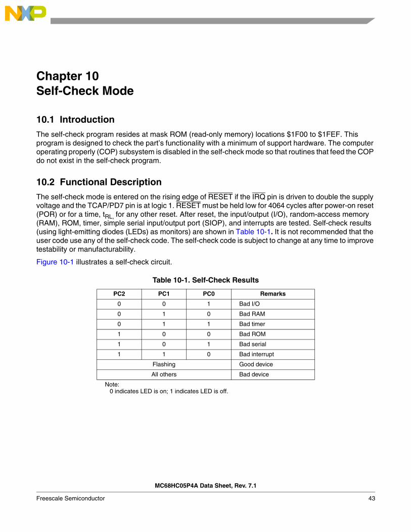
The self-check mode is entered on the rising edge of RESET if the IRQ pin is driven to double the supply voltage and the TCAP/PD7 pin is at logic 1. RESET must be held low for 4064 cycles after power-on reset (POR) or for a time, tRL, for any other reset. After reset, the input/output (I/O), random-access memory (RAM), ROM, timer, simple serial input/output port (SIOP), and interrupts are tested. Self-check results (using light-emitting diodes (LEDs) as monitors) are shown in Table 10-1. It is not recommended that the user code use any of the self-check code. The self-check code is subject to change at any time to improve testability or manufacturability.
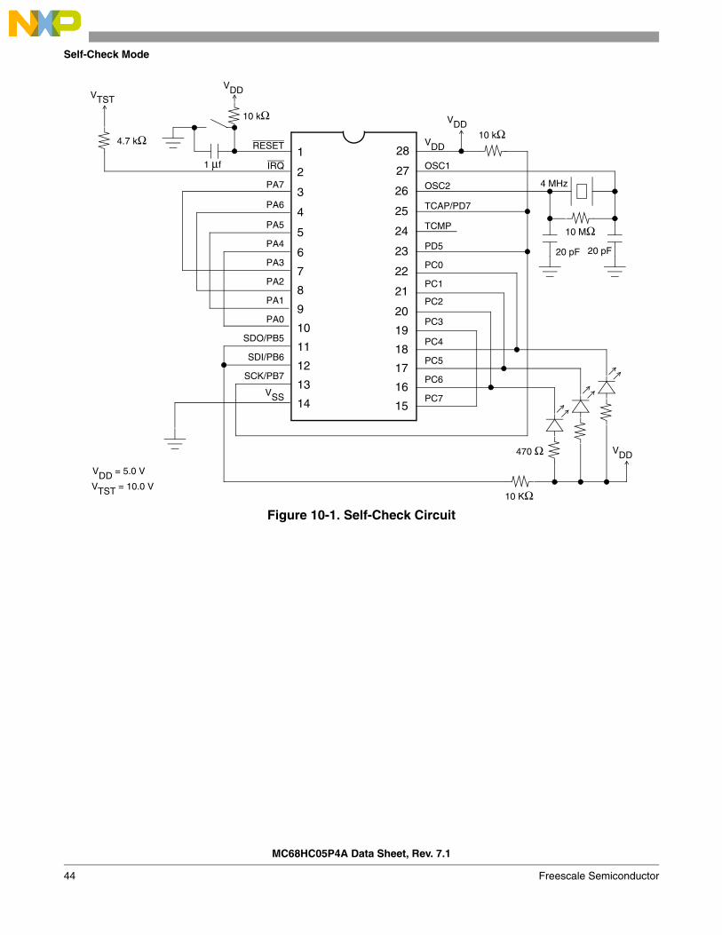
Figure 10-1 illustrates a self-check circuit.
Table 10-1. Self-Check Results
PC2 PC1 PC0 Remarks
0 0 1 Bad I/O
0 1 0 Bad RAM
0 1 1 Bad timer
1 0 0 Bad ROM
1 0 1 Bad serial
1 1 0 Bad interrupt
Flashing Good device
All others Bad device
Note:0 indicates LED is on; 1 indicates LED is off.
Self-Check Mode
MC68HC05P4A Data Sheet, Rev. 7.1
44 Freescale Semiconductor
Figure 10-1. Self-Check Circuit
10 kΩ
VDD
1
2
3
4
5
6
7
8
9
10
11
12
13
14
27
28
21
22
23
24
25
26
VDD
4.7 kΩ RESET
IRQ
PA5
PA4
PA3
PA2
PA1
PA0
PA6
PA7
SDO/PB5
SDI/PB6
SCK/PB7
VSS
1 µf
20 pF
10 MΩ
4 MHz
20 pF
PC0
VDD
OSC1
OSC2
TCAP/PD7
TCMP
PD5
PC1
PC2
PC3
PC4
PC5
PC6
PC7
VDD
VTST
20
19
18
17
16
15
10 KΩ
470 Ω
10 kΩ
VTST = 10.0 V
VDD = 5.0 V
MC68HC05P4A Data Sheet, Rev. 7.1
Freescale Semiconductor 45
Chapter 11 Instruction Set
11.1 Introduction
This section describes the M68HC05P4A addressing modes and instruction types.
11.2 Addressing Modes
The CPU uses eight addressing modes for flexibility in accessing data. The addressing modes define the manner in which the CPU finds the data required to execute an instruction. The addressing modes are:
1. Inherent2. Immediate3. Direct4. Extended5. Indexed, no offset6. Indexed, 8-bit offset7. Indexed, 16-bit offset8. Relative
11.2.1 Inherent
Inherent instructions are those that have no operand, such as return from interrupt (RTI) and stop (STOP). Some of the inherent instructions act on data in the CPU registers, such as set carry flag (SEC) and increment accumulator (INCA). Inherent instructions require no memory address and are one byte long.
11.2.2 Immediate
Immediate instructions are those that contain a value to be used in an operation with the value in the accumulator or index register. Immediate instructions require no memory address and are two bytes long. The opcode is the first byte, and the immediate data value is the second byte.
11.2.3 Direct
Direct instructions can access any of the first 256 memory addresses with two bytes. The first byte is the opcode, and the second is the low byte of the operand address. In direct addressing, the CPU automatically uses $00 as the high byte of the operand address. BRSET and BRCLR are 3-byte instructions that use direct addressing to access the operand and relative addressing to specify a branch destination.
Instruction Set
MC68HC05P4A Data Sheet, Rev. 7.1
46 Freescale Semiconductor
11.2.4 Extended
Extended instructions use only three bytes to access any address in memory. The first byte is the opcode; the second and third bytes are the high and low bytes of the operand address.
When using the Freescale assembler, the programmer does not need to specify whether an instruction is direct or extended. The assembler automatically selects the shortest form of the instruction.
11.2.5 Indexed, No Offset
Indexed instructions with no offset are one-byte instructions that can access data with variable addresses within the first 256 memory locations. The index register contains the low byte of the conditional address of the operand. The CPU automatically uses $00 as the high byte, so these instructions can address locations $0000–$00FF.
Indexed, no offset instructions are often used to move a pointer through a table or to hold the address of a frequently used RAM or I/O location.
11.2.6 Indexed, 8-Bit Offset
Indexed, 8-bit offset instructions are 2-byte instructions that can access data with variable addresses within the first 511 memory locations. The CPU adds the unsigned byte in the index register to the unsigned byte following the opcode. The sum is the conditional address of the operand. These instructions can access locations $0000–$01FE.
Indexed 8-bit offset instructions are useful for selecting the kth element in an n-element table. The table can begin anywhere within the first 256 memory locations and could extend as far as location 510 ($01FE). The k value is typically in the index register, and the address of the beginning of the table is in the byte following the opcode.
11.2.7 Indexed, 16-Bit Offset
Indexed, 16-bit offset instructions are 3-byte instructions that can access data with variable addresses at any location in memory. The CPU adds the unsigned byte in the index register to the two unsigned bytes following the opcode. The sum is the conditional address of the operand. The first byte after the opcode is the high byte of the 16-bit offset; the second byte is the low byte of the offset. These instructions can address any location in memory.
Indexed, 16-bit offset instructions are useful for selecting the kth element in an n-element table anywhere in memory.
As with direct and extended addressing the Freescale assembler determines the shortest form of indexed addressing.
11.2.8 Relative
Relative addressing is only for branch instructions. If the branch condition is true, the CPU finds the conditional branch destination by adding the signed byte following the opcode to the contents of the program counter. If the branch condition is not true, the CPU goes to the next instruction. The offset is a signed, two’s complement byte that gives a branching range of –128 to +127 bytes from the address of the next location after the branch instruction.
When using the Freescale assembler, the programmer does not need to calculate the offset, because the assembler determines the proper offset and verifies that it is within the span of the branch.
Instruction Types
MC68HC05P4A Data Sheet, Rev. 7.1
Freescale Semiconductor 47
11.3 Instruction Types
The MCU instructions fall into five categories:1. Register/memory instructions2. Read-modify-write instructions3. Jump/branch instructions4. Bit manipulation instructions5. Control instructions
11.3.1 Register/Memory Instructions
Most of these instructions use two operands. One operand is in either the accumulator or the index register. The CPU finds the other operand in memory. Table 11-1 lists the register/memory instructions.
Table 11-1. Register/Memory Instructions
Instruction Mnemonic
Add memory byte and carry bit to accumulator ADC
Add memory byte to accumulator ADD
AND memory byte with accumulator AND
Bit test accumulator BIT
Compare accumulator CMP
Compare index register with memory byte CPX
EXCLUSIVE OR accumulator with memory byte EOR
Load accumulator with memory byte LDA
Load index register with memory byte LDX
Multiply MUL
OR accumulator with memory byte ORA
Subtract memory byte and carry bit from accumulator SBC
Store accumulator in memory STA
Store index register in memory STX
Subtract memory byte from accumulator SUB
Instruction Set
MC68HC05P4A Data Sheet, Rev. 7.1
48 Freescale Semiconductor
11.3.2 Read-Modify-Write Instructions
These instructions read a memory location or a register, modify its contents, and write the modified value back to the memory location or to the register. The test for negative or zero instruction (TST) is an exception to the read-modify-write sequence because it does not write a replacement value. Table 11-2 lists the read-modify-write instructions.
Table 11-2. Read-Modify-Write Instructions
Instruction Mnemonic
Arithmetic shift left ASL
Arithmetic shift right ASR
Clear bit in memory BCLR
Set bit in memory BSET
Clear CLR
Complement (one’s complement) COM
Decrement DEC
Increment INC
Logical shift left LSL
Logical shift right LSR
Negate (two’s complement) NEG
Rotate left through carry bit ROL
Rotate right through carry bit ROR
Test for negative or zero TST
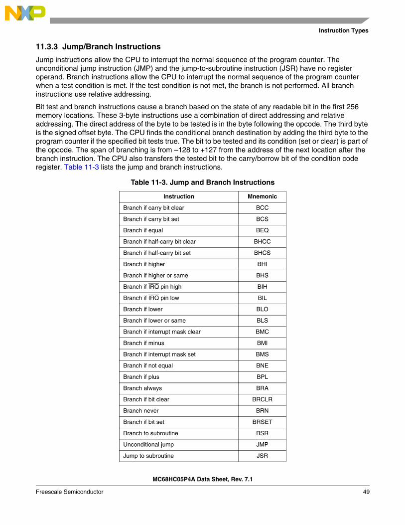
Instruction Types
MC68HC05P4A Data Sheet, Rev. 7.1
Freescale Semiconductor 49
11.3.3 Jump/Branch Instructions
Jump instructions allow the CPU to interrupt the normal sequence of the program counter. The unconditional jump instruction (JMP) and the jump-to-subroutine instruction (JSR) have no register operand. Branch instructions allow the CPU to interrupt the normal sequence of the program counter when a test condition is met. If the test condition is not met, the branch is not performed. All branch instructions use relative addressing.
Bit test and branch instructions cause a branch based on the state of any readable bit in the first 256 memory locations. These 3-byte instructions use a combination of direct addressing and relative addressing. The direct address of the byte to be tested is in the byte following the opcode. The third byte is the signed offset byte. The CPU finds the conditional branch destination by adding the third byte to the program counter if the specified bit tests true. The bit to be tested and its condition (set or clear) is part of the opcode. The span of branching is from –128 to +127 from the address of the next location after the branch instruction. The CPU also transfers the tested bit to the carry/borrow bit of the condition code register. Table 11-3 lists the jump and branch instructions.
Table 11-3. Jump and Branch Instructions
Instruction Mnemonic
Branch if carry bit clear BCC
Branch if carry bit set BCS
Branch if equal BEQ
Branch if half-carry bit clear BHCC
Branch if half-carry bit set BHCS
Branch if higher BHI
Branch if higher or same BHS
Branch if IRQ pin high BIH
Branch if IRQ pin low BIL
Branch if lower BLO
Branch if lower or same BLS
Branch if interrupt mask clear BMC
Branch if minus BMI
Branch if interrupt mask set BMS
Branch if not equal BNE
Branch if plus BPL
Branch always BRA
Branch if bit clear BRCLR
Branch never BRN
Branch if bit set BRSET
Branch to subroutine BSR
Unconditional jump JMP
Jump to subroutine JSR
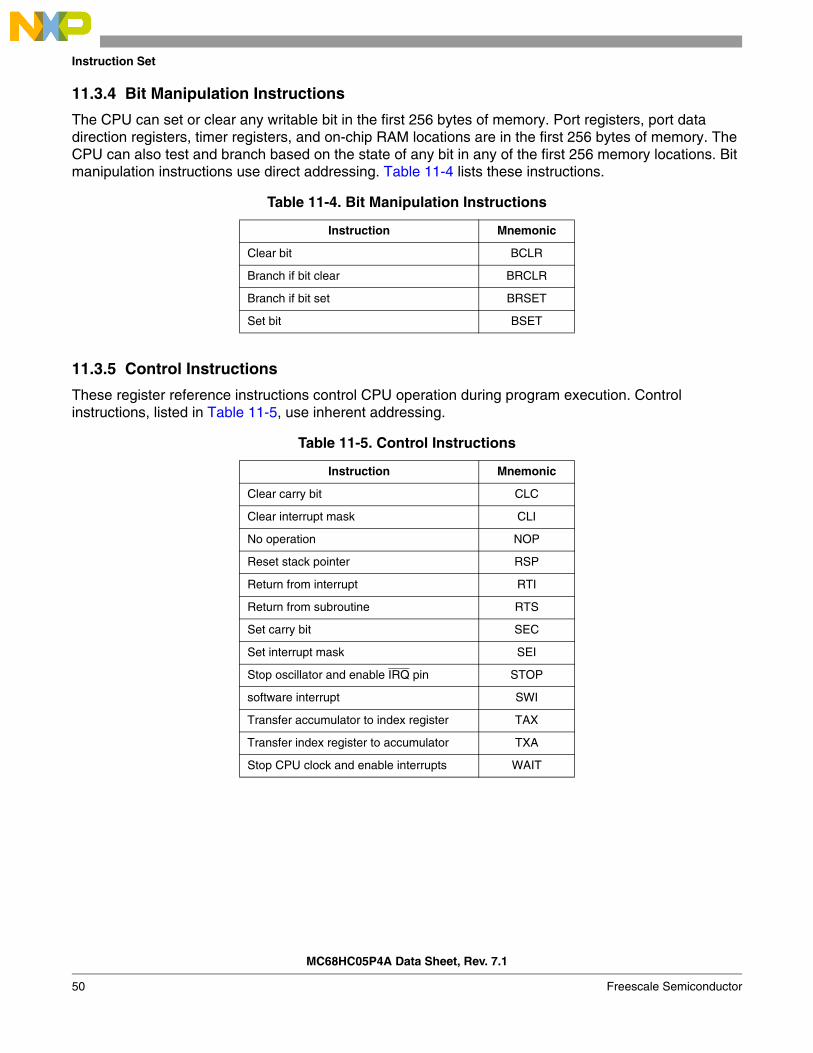
Instruction Set
MC68HC05P4A Data Sheet, Rev. 7.1
50 Freescale Semiconductor
11.3.4 Bit Manipulation Instructions
The CPU can set or clear any writable bit in the first 256 bytes of memory. Port registers, port data direction registers, timer registers, and on-chip RAM locations are in the first 256 bytes of memory. The CPU can also test and branch based on the state of any bit in any of the first 256 memory locations. Bit manipulation instructions use direct addressing. Table 11-4 lists these instructions.
11.3.5 Control Instructions
These register reference instructions control CPU operation during program execution. Control instructions, listed in Table 11-5, use inherent addressing.
Table 11-4. Bit Manipulation Instructions
Instruction Mnemonic
Clear bit BCLR
Branch if bit clear BRCLR
Branch if bit set BRSET
Set bit BSET
Table 11-5. Control Instructions
Instruction Mnemonic
Clear carry bit CLC
Clear interrupt mask CLI
No operation NOP
Reset stack pointer RSP
Return from interrupt RTI
Return from subroutine RTS
Set carry bit SEC
Set interrupt mask SEI
Stop oscillator and enable IRQ pin STOP
software interrupt SWI
Transfer accumulator to index register TAX
Transfer index register to accumulator TXA
Stop CPU clock and enable interrupts WAIT
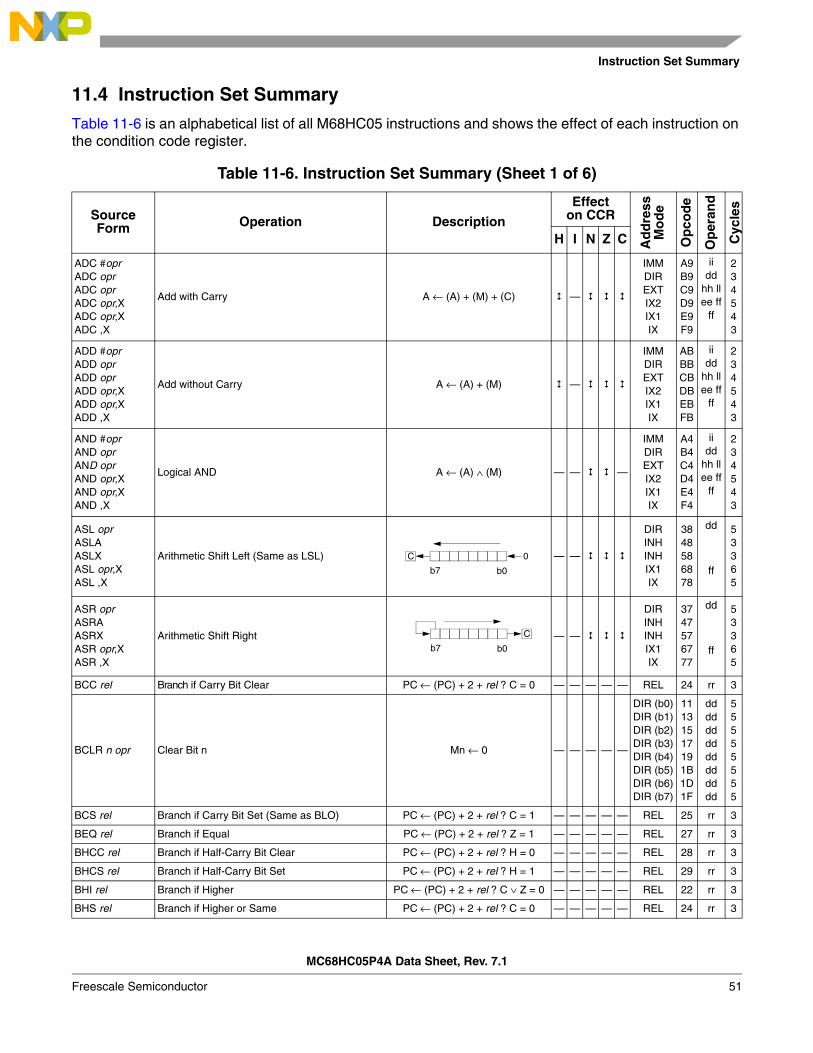
Instruction Set Summary
MC68HC05P4A Data Sheet, Rev. 7.1
Freescale Semiconductor 51
11.4 Instruction Set Summary
Table 11-6 is an alphabetical list of all M68HC05 instructions and shows the effect of each instruction on the condition code register.
Table 11-6. Instruction Set Summary (Sheet 1 of 6)
SourceForm Operation Description
Effecton CCR
Ad
dre
ssM
od
e
Op
cod
e
Op
eran
d
Cyc
les
H I N Z C
ADC #oprADC oprADC oprADC opr,XADC opr,XADC ,X
Add with Carry A ← (A) + (M) + (C) —
IMMDIREXTIX2IX1IX
A9B9C9D9E9F9
iidd
hh llee ff
ff
234543
ADD #oprADD oprADD oprADD opr,XADD opr,XADD ,X
Add without Carry A ← (A) + (M) —
IMMDIREXTIX2IX1IX
ABBBCBDBEBFB
iidd
hh llee ff
ff
234543
AND #oprAND oprAND oprAND opr,XAND opr,XAND ,X
Logical AND A ← (A) ∧ (M) — — —
IMMDIREXTIX2IX1IX
A4B4C4D4E4F4
iidd
hh llee ff
ff
234543
ASL oprASLAASLXASL opr,XASL ,X
Arithmetic Shift Left (Same as LSL) — —
DIRINHINHIX1IX
3848586878
dd
ff
53365
ASR oprASRAASRXASR opr,XASR ,X
Arithmetic Shift Right — —
DIRINHINHIX1IX
3747576777
dd
ff
53365
BCC rel Branch if Carry Bit Clear PC ← (PC) + 2 + rel ? C = 0 — — — — — REL 24 rr 3
BCLR n opr Clear Bit n Mn ← 0 — — — — —
DIR (b0)DIR (b1)DIR (b2)DIR (b3)DIR (b4)DIR (b5)DIR (b6)DIR (b7)
11131517191B1D1F
dddddddddddddddd
55555555
BCS rel Branch if Carry Bit Set (Same as BLO) PC ← (PC) + 2 + rel ? C = 1 — — — — — REL 25 rr 3
BEQ rel Branch if Equal PC ← (PC) + 2 + rel ? Z = 1 — — — — — REL 27 rr 3
BHCC rel Branch if Half-Carry Bit Clear PC ← (PC) + 2 + rel ? H = 0 — — — — — REL 28 rr 3
BHCS rel Branch if Half-Carry Bit Set PC ← (PC) + 2 + rel ? H = 1 — — — — — REL 29 rr 3
BHI rel Branch if Higher PC ← (PC) + 2 + rel ? C ∨ Z = 0 — — — — — REL 22 rr 3
BHS rel Branch if Higher or Same PC ← (PC) + 2 + rel ? C = 0 — — — — — REL 24 rr 3
C
b0b7
0
b0b7
C
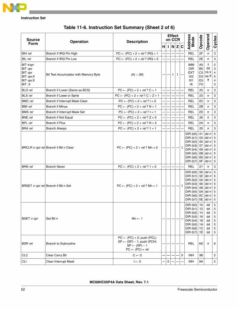
Instruction Set
MC68HC05P4A Data Sheet, Rev. 7.1
52 Freescale Semiconductor
BIH rel Branch if IRQ Pin High PC ← (PC) + 2 + rel ? IRQ = 1 — — — — — REL 2F rr 3
BIL rel Branch if IRQ Pin Low PC ← (PC) + 2 + rel ? IRQ = 0 — — — — — REL 2E rr 3
BIT #oprBIT oprBIT oprBIT opr,XBIT opr,XBIT ,X
Bit Test Accumulator with Memory Byte (A) ∧ (M) — — —
IMMDIREXTIX2IX1IX
A5B5C5D5E5F5
iidd
hh llee ff
ff
234543
BLO rel Branch if Lower (Same as BCS) PC ← (PC) + 2 + rel ? C = 1 — — — — — REL 25 rr 3
BLS rel Branch if Lower or Same PC ← (PC) + 2 + rel ? C ∨ Z = 1 — — — — — REL 23 rr 3
BMC rel Branch if Interrupt Mask Clear PC ← (PC) + 2 + rel ? I = 0 — — — — — REL 2C rr 3
BMI rel Branch if Minus PC ← (PC) + 2 + rel ? N = 1 — — — — — REL 2B rr 3
BMS rel Branch if Interrupt Mask Set PC ← (PC) + 2 + rel ? I = 1 — — — — — REL 2D rr 3
BNE rel Branch if Not Equal PC ← (PC) + 2 + rel ? Z = 0 — — — — — REL 26 rr 3
BPL rel Branch if Plus PC ← (PC) + 2 + rel ? N = 0 — — — — — REL 2A rr 3
BRA rel Branch Always PC ← (PC) + 2 + rel ? 1 = 1 — — — — — REL 20 rr 3
BRCLR n opr rel Branch if Bit n Clear PC ← (PC) + 2 + rel ? Mn = 0 — — — —
DIR (b0)DIR (b1)DIR (b2)DIR (b3)DIR (b4)DIR (b5)DIR (b6)DIR (b7)
01030507090B0D0F
dd rrdd rrdd rrdd rrdd rrdd rrdd rrdd rr
55555555
BRN rel Branch Never PC ← (PC) + 2 + rel ? 1 = 0 — — — — — REL 21 rr 3
BRSET n opr rel Branch if Bit n Set PC ← (PC) + 2 + rel ? Mn = 1 — — — —
DIR (b0)DIR (b1)DIR (b2)DIR (b3)DIR (b4)DIR (b5)DIR (b6)DIR (b7)
00020406080A0C0E
dd rrdd rrdd rrdd rrdd rrdd rrdd rrdd rr
55555555
BSET n opr Set Bit n Mn ← 1 — — — — —
DIR (b0)DIR (b1)DIR (b2)DIR (b3)DIR (b4)DIR (b5)DIR (b6)DIR (b7)
10121416181A1C1E
dddddddddddddddd
55555555
BSR rel Branch to Subroutine
PC ← (PC) + 2; push (PCL)SP ← (SP) – 1; push (PCH)
SP ← (SP) – 1PC ← (PC) + rel
— — — — — REL AD rr 6
CLC Clear Carry Bit C ← 0 — — — — 0 INH 98 2
CLI Clear Interrupt Mask I ← 0 — 0 — — — INH 9A 2
Table 11-6. Instruction Set Summary (Sheet 2 of 6)
SourceForm Operation Description
Effecton CCR
Ad
dre
ssM
od
e
Op
cod
e
Op
eran
d
Cyc
les
H I N Z C
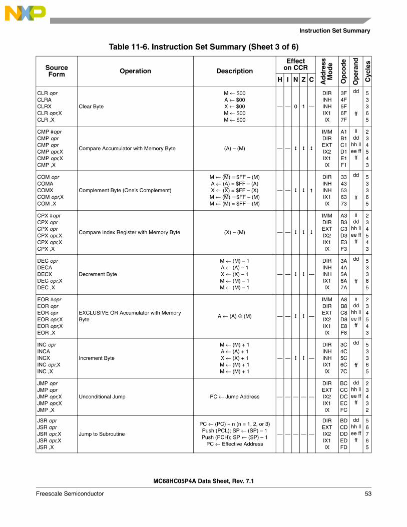
Instruction Set Summary
MC68HC05P4A Data Sheet, Rev. 7.1
Freescale Semiconductor 53
CLR oprCLRACLRXCLR opr,XCLR ,X
Clear Byte
M ← $00A ← $00X ← $00M ← $00M ← $00
— — 0 1 —
DIRINHINHIX1IX
3F4F5F6F7F
dd
ff
53365
CMP #oprCMP oprCMP oprCMP opr,XCMP opr,XCMP ,X
Compare Accumulator with Memory Byte (A) – (M) — —
IMMDIREXTIX2IX1IX
A1B1C1D1E1F1
iidd
hh llee ff
ff
234543
COM oprCOMACOMXCOM opr,XCOM ,X
Complement Byte (One’s Complement)
M ← (M) = $FF – (M)A ← (A) = $FF – (A)X ← (X) = $FF – (X)M ← (M) = $FF – (M)M ← (M) = $FF – (M)
— — 1
DIRINHINHIX1IX
3343536373
dd
ff
53365
CPX #oprCPX oprCPX oprCPX opr,XCPX opr,XCPX ,X
Compare Index Register with Memory Byte (X) – (M) — —
IMMDIREXTIX2IX1IX
A3B3C3D3E3F3
iidd
hh llee ff
ff
234543
DEC oprDECADECXDEC opr,XDEC ,X
Decrement Byte
M ← (M) – 1A ← (A) – 1X ← (X) – 1M ← (M) – 1M ← (M) – 1
— — —
DIRINHINHIX1IX
3A4A5A6A7A
dd
ff
53365
EOR #oprEOR oprEOR oprEOR opr,XEOR opr,XEOR ,X
EXCLUSIVE OR Accumulator with Memory Byte
A ← (A) ⊕ (M) — — —
IMMDIREXTIX2IX1IX
A8B8C8D8E8F8
iidd
hh llee ff
ff
234543
INC oprINCAINCXINC opr,XINC ,X
Increment Byte
M ← (M) + 1A ← (A) + 1X ← (X) + 1M ← (M) + 1M ← (M) + 1
— — —
DIRINHINHIX1IX
3C4C5C6C7C
dd
ff
53365
JMP oprJMP oprJMP opr,XJMP opr,XJMP ,X
Unconditional Jump PC ← Jump Address — — — — —
DIREXTIX2IX1IX
BCCCDCECFC
ddhh llee ff
ff
23432
JSR oprJSR oprJSR opr,XJSR opr,XJSR ,X
Jump to Subroutine
PC ← (PC) + n (n = 1, 2, or 3)Push (PCL); SP ← (SP) – 1Push (PCH); SP ← (SP) – 1
PC ← Effective Address
— — — — —
DIREXTIX2IX1IX
BDCDDDEDFD
ddhh llee ff
ff
56765
Table 11-6. Instruction Set Summary (Sheet 3 of 6)
SourceForm Operation Description
Effecton CCR
Ad
dre
ssM
od
e
Op
cod
e
Op
eran
d
Cyc
les
H I N Z C
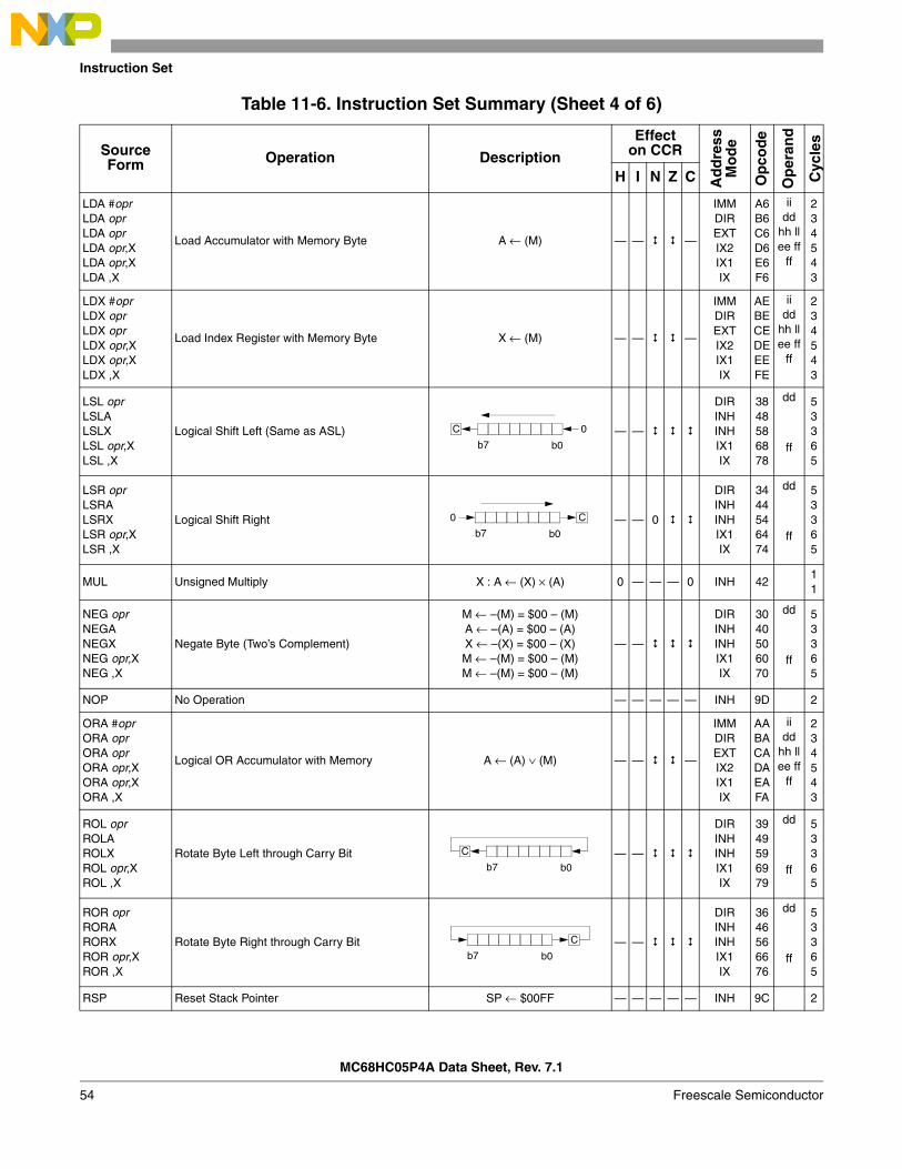
Instruction Set
MC68HC05P4A Data Sheet, Rev. 7.1
54 Freescale Semiconductor
LDA #oprLDA oprLDA oprLDA opr,XLDA opr,XLDA ,X
Load Accumulator with Memory Byte A ← (M) — — —
IMMDIREXTIX2IX1IX
A6B6C6D6E6F6
iidd
hh llee ff
ff
234543
LDX #oprLDX oprLDX oprLDX opr,XLDX opr,XLDX ,X
Load Index Register with Memory Byte X ← (M) — — —
IMMDIREXTIX2IX1IX
AEBECEDEEEFE
iidd
hh llee ff
ff
234543
LSL oprLSLALSLXLSL opr,XLSL ,X
Logical Shift Left (Same as ASL) — —
DIRINHINHIX1IX
3848586878
dd
ff
53365
LSR oprLSRALSRXLSR opr,XLSR ,X
Logical Shift Right — — 0
DIRINHINHIX1IX
3444546474
dd
ff
53365
MUL Unsigned Multiply X : A ← (X) × (A) 0 — — — 0 INH 4211
NEG oprNEGANEGXNEG opr,XNEG ,X
Negate Byte (Two’s Complement)
M ← –(M) = $00 – (M)A ← –(A) = $00 – (A)X ← –(X) = $00 – (X)M ← –(M) = $00 – (M)M ← –(M) = $00 – (M)
— —
DIRINHINHIX1IX
3040506070
dd
ff
53365
NOP No Operation — — — — — INH 9D 2
ORA #oprORA oprORA oprORA opr,XORA opr,XORA ,X
Logical OR Accumulator with Memory A ← (A) ∨ (M) — — —
IMMDIREXTIX2IX1IX
AABACADAEAFA
iidd
hh llee ff
ff
234543
ROL oprROLAROLXROL opr,XROL ,X
Rotate Byte Left through Carry Bit — —
DIRINHINHIX1IX
3949596979
dd
ff
53365
ROR oprRORARORXROR opr,XROR ,X
Rotate Byte Right through Carry Bit — —
DIRINHINHIX1IX
3646566676
dd
ff
53365
RSP Reset Stack Pointer SP ← $00FF — — — — — INH 9C 2
Table 11-6. Instruction Set Summary (Sheet 4 of 6)
SourceForm Operation Description
Effecton CCR
Ad
dre
ssM
od
e
Op
cod
e
Op
eran
d
Cyc
les
H I N Z C
C
b0b7
0
b0b7
C0
C
b0b7
b0b7
C
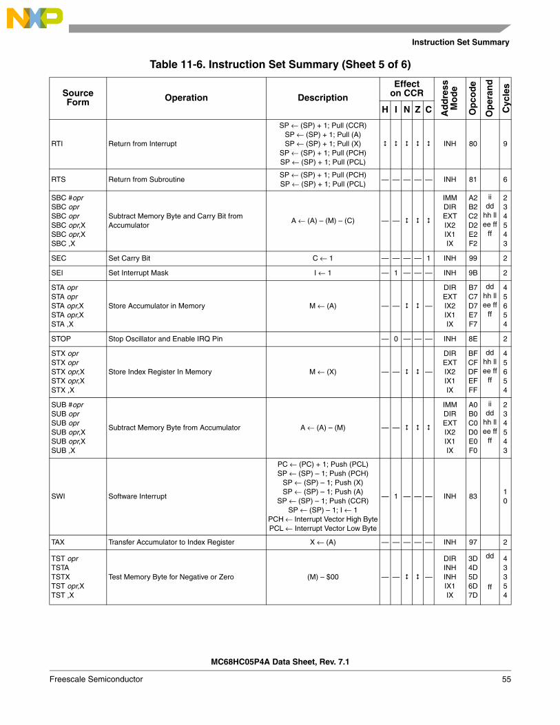
Instruction Set Summary
MC68HC05P4A Data Sheet, Rev. 7.1
Freescale Semiconductor 55
RTI Return from Interrupt
SP ← (SP) + 1; Pull (CCR)SP ← (SP) + 1; Pull (A)SP ← (SP) + 1; Pull (X)
SP ← (SP) + 1; Pull (PCH)SP ← (SP) + 1; Pull (PCL)
INH 80 9
RTS Return from SubroutineSP ← (SP) + 1; Pull (PCH)SP ← (SP) + 1; Pull (PCL)
— — — — — INH 81 6
SBC #oprSBC oprSBC oprSBC opr,XSBC opr,XSBC ,X
Subtract Memory Byte and Carry Bit from Accumulator
A ← (A) – (M) – (C) — —
IMMDIREXTIX2IX1IX
A2B2C2D2E2F2
iidd
hh llee ff
ff
234543
SEC Set Carry Bit C ← 1 — — — — 1 INH 99 2
SEI Set Interrupt Mask I ← 1 — 1 — — — INH 9B 2
STA oprSTA oprSTA opr,XSTA opr,XSTA ,X
Store Accumulator in Memory M ← (A) — — —
DIREXTIX2IX1IX
B7C7D7E7F7
ddhh llee ff
ff
45654
STOP Stop Oscillator and Enable IRQ Pin — 0 — — — INH 8E 2
STX oprSTX oprSTX opr,XSTX opr,XSTX ,X
Store Index Register In Memory M ← (X) — — —
DIREXTIX2IX1IX
BFCFDFEFFF
ddhh llee ff
ff
45654
SUB #oprSUB oprSUB oprSUB opr,XSUB opr,XSUB ,X
Subtract Memory Byte from Accumulator A ← (A) – (M) — —
IMMDIREXTIX2IX1IX
A0B0C0D0E0F0
iidd
hh llee ff
ff
234543
SWI Software Interrupt
PC ← (PC) + 1; Push (PCL)SP ← (SP) – 1; Push (PCH)
SP ← (SP) – 1; Push (X)SP ← (SP) – 1; Push (A)
SP ← (SP) – 1; Push (CCR)SP ← (SP) – 1; I ← 1
PCH ← Interrupt Vector High BytePCL ← Interrupt Vector Low Byte
— 1 — — — INH 8310
TAX Transfer Accumulator to Index Register X ← (A) — — — — — INH 97 2
TST oprTSTATSTXTST opr,XTST ,X
Test Memory Byte for Negative or Zero (M) – $00 — — —
DIRINHINHIX1IX
3D4D5D6D7D
dd
ff
43354
Table 11-6. Instruction Set Summary (Sheet 5 of 6)
SourceForm Operation Description
Effecton CCR
Ad
dre
ssM
od
e
Op
cod
e
Op
eran
d
Cyc
les
H I N Z C
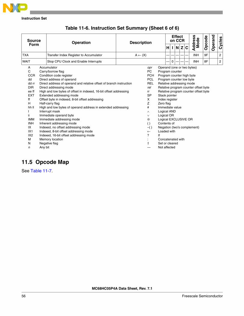
Instruction Set
MC68HC05P4A Data Sheet, Rev. 7.1
56 Freescale Semiconductor
11.5 Opcode Map
See Table 11-7.
TXA Transfer Index Register to Accumulator A ← (X) — — — — — INH 9F 2
WAIT Stop CPU Clock and Enable Interrupts — 0 — — — INH 8F 2
A Accumulator opr Operand (one or two bytes)C Carry/borrow flag PC Program counterCCR Condition code register PCH Program counter high bytedd Direct address of operand PCL Program counter low bytedd rr Direct address of operand and relative offset of branch instruction REL Relative addressing modeDIR Direct addressing mode rel Relative program counter offset byteee ff High and low bytes of offset in indexed, 16-bit offset addressing rr Relative program counter offset byteEXT Extended addressing mode SP Stack pointerff Offset byte in indexed, 8-bit offset addressing X Index registerH Half-carry flag Z Zero flaghh ll High and low bytes of operand address in extended addressing # Immediate valueI Interrupt mask ∧ Logical ANDii Immediate operand byte ∨ Logical ORIMM Immediate addressing mode ⊕ Logical EXCLUSIVE ORINH Inherent addressing mode ( ) Contents ofIX Indexed, no offset addressing mode –( ) Negation (two’s complement)IX1 Indexed, 8-bit offset addressing mode ← Loaded withIX2 Indexed, 16-bit offset addressing mode ? IfM Memory location : Concatenated withN Negative flag Set or clearedn Any bit — Not affected
Table 11-6. Instruction Set Summary (Sheet 6 of 6)
SourceForm Operation Description
Effecton CCR
Ad
dre
ssM
od
e
Op
cod
e
Op
eran
d
Cyc
les
H I N Z C
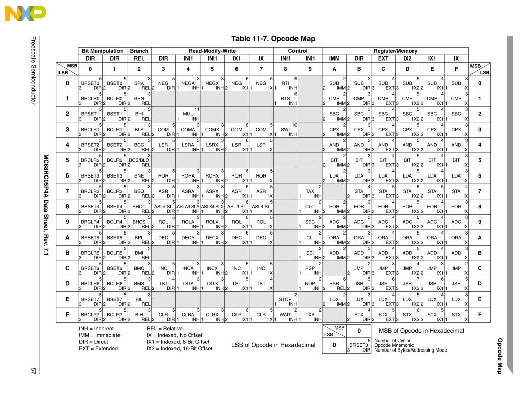
MC
68HC
05P4A
Data S
heet, R
ev. 7.1
Freescale S
emiconductor
57
Op
cod
e Map
Table 11-7. Opcode Map
Bit Manipulation Branch Read-Modify-Write Control Register/MemoryDIR DIR REL DIR INH INH IX1 IX INH INH IMM DIR EXT IX2 IX1 IX
0 1 2 3 4 5 6 7 8 9 A B C D E F
05
BRSET03 DIR
5BSET0
2 DIR
3BRA
2 REL
5NEG
2 DIR
3NEGA
1 INH
3NEGX
1 INH
6NEG
2 IX1
5NEG
1 IX
9RTI
1 INH
2SUB
2 IMM
3SUB
2 DIR
4SUB
3 EXT
5SUB
3 IX2
4SUB
2 IX1
3SUB
1 IX0
15
BRCLR03 DIR
5BCLR0
2 DIR
3BRN
2 REL
6RTS
1 INH
2CMP
2 IMM
3CMP
2 DIR
4CMP
3 EXT
5CMP
3 IX2
4CMP
2 IX1
3CMP
1 IX1
25
BRSET13 DIR
5BSET1
2 DIR
3BHI
2 REL
11MUL
1 INH
2SBC
2 IMM
3SBC
2 DIR
4SBC
3 EXT
5SBC
3 IX2
4SBC
2 IX1
3SBC
1 IX2
35
BRCLR13 DIR
5BCLR1
2 DIR
3BLS
2 REL
5COM
2 DIR
3COMA
1 INH
3COMX
1 INH
6COM
2 IX1
5COM
1 IX
10SWI
1 INH
2CPX
2 IMM
3CPX
2 DIR
4CPX
3 EXT
5CPX
3 IX2
4CPX
2 IX1
3CPX
1 IX3
45
BRSET23 DIR
5BSET2
2 DIR
3BCC
2 REL
5LSR
2 DIR
3LSRA
1 INH
3LSRX
1 INH
6LSR
2 IX1
5LSR
1 IX
2AND
2 IMM
3AND
2 DIR
4AND
3 EXT
5AND
3 IX2
4AND
2 IX1
3AND
1 IX4
55
BRCLR23 DIR
5BCLR2
2 DIR
3BCS/BLO2 REL
2BIT
2 IMM
3BIT
2 DIR
4BIT
3 EXT
5BIT
3 IX2
4BIT
2 IX1
3BIT
1 IX5
65
BRSET33 DIR
5BSET3
2 DIR
3BNE
2 REL
5ROR
2 DIR
3RORA
1 INH
3RORX
1 INH
6ROR
2 IX1
5ROR
1 IX
2LDA
2 IMM
3LDA
2 DIR
4LDA
3 EXT
5LDA
3 IX2
4LDA
2 IX1
3LDA
1 IX6
75
BRCLR33 DIR
5BCLR3
2 DIR
3BEQ
2 REL
5ASR
2 DIR
3ASRA
1 INH
3ASRX
1 INH
6ASR
2 IX1
5ASR
1 IX
2TAX
1 INH
4STA
2 DIR
5STA
3 EXT
6STA
3 IX2
5STA
2 IX1
4STA
1 IX7
85
BRSET43 DIR
5BSET4
2 DIR
3BHCC
2 REL
5ASL/LSL
2 DIR
3ASLA/LSLA1 INH
3ASLX/LSLX1 INH
6ASL/LSL
2 IX1
5ASL/LSL
1 IX
2CLC
1 INH
2EOR
2 IMM
3EOR
2 DIR
4EOR
3 EXT
5EOR
3 IX2
4EOR
2 IX1
3EOR
1 IX8
95
BRCLR43 DIR
5BCLR4
2 DIR
3BHCS
2 REL
5ROL
2 DIR
3ROLA
1 INH
3ROLX
1 INH
6ROL
2 IX1
5ROL
1 IX
2SEC
1 INH
2ADC
2 IMM
3ADC
2 DIR
4ADC
3 EXT
5ADC
3 IX2
4ADC
2 IX1
3ADC
1 IX9
A5
BRSET53 DIR
5BSET5
2 DIR
3BPL
2 REL
5DEC
2 DIR
3DECA
1 INH
3DECX
1 INH
6DEC
2 IX1
5DEC
1 IX
2CLI
1 INH
2ORA
2 IMM
3ORA
2 DIR
4ORA
3 EXT
5ORA
3 IX2
4ORA
2 IX1
3ORA
1 IXA
B5
BRCLR53 DIR
5BCLR5
2 DIR
3BMI
2 REL
2SEI
1 INH
2ADD
2 IMM
3ADD
2 DIR
4ADD
3 EXT
5ADD
3 IX2
4ADD
2 IX1
3ADD
1 IXB
C5
BRSET63 DIR
5BSET6
2 DIR
3BMC
2 REL
5INC
2 DIR
3INCA
1 INH
3INCX
1 INH
6INC
2 IX1
5INC
1 IX
2RSP
1 INH
2JMP
2 DIR
3JMP
3 EXT
4JMP
3 IX2
3JMP
2 IX1
2JMP
1 IXC
D5
BRCLR63 DIR
5BCLR6
2 DIR
3BMS
2 REL
4TST
2 DIR
3TSTA
1 INH
3TSTX
1 INH
5TST
2 IX1
4TST
1 IX
2NOP
1 INH
6BSR
2 REL
5JSR
2 DIR
6JSR
3 EXT
7JSR
3 IX2
6JSR
2 IX1
5JSR
1 IXD
E5
BRSET73 DIR
5BSET7
2 DIR
3BIL
2 REL
2STOP
1 INH
2LDX
2 IMM
3LDX
2 DIR
4LDX
3 EXT
5LDX
3 IX2
4LDX
2 IX1
3LDX
1 IXE
F5
BRCLR73 DIR
5BCLR7
2 DIR
3BIH
2 REL
5CLR
2 DIR
3CLRA
1 INH
3CLRX
1 INH
6CLR
2 IX1
5CLR
1 IX
2WAIT
1 INH
2TXA
1 INH
4STX
2 DIR
5STX
3 EXT
6STX
3 IX2
5STX
2 IX1
4STX
1 IXF
INH = Inherent REL = RelativeIMM = Immediate IX = Indexed, No OffsetDIR = Direct IX1 = Indexed, 8-Bit OffsetEXT = Extended IX2 = Indexed, 16-Bit Offset
0 MSB of Opcode in Hexadecimal
LSB of Opcode in Hexadecimal 05
BRSET03 DIR
Number of CyclesOpcode MnemonicNumber of Bytes/Addressing Mode
LSBMSB
LSBMSB
LSB
MSB

Instruction Set
MC68HC05P4A Data Sheet, Rev. 7.1
58 Freescale Semiconductor
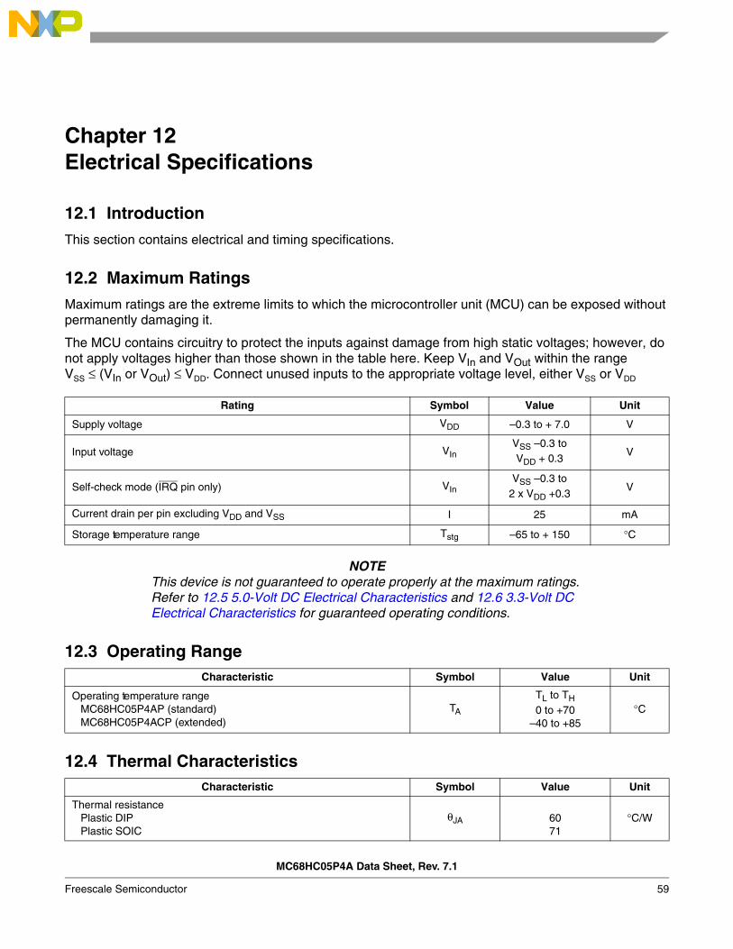
MC68HC05P4A Data Sheet, Rev. 7.1
Freescale Semiconductor 59
Chapter 12 Electrical Specifications
12.1 Introduction
This section contains electrical and timing specifications.
12.2 Maximum Ratings
Maximum ratings are the extreme limits to which the microcontroller unit (MCU) can be exposed without permanently damaging it.
The MCU contains circuitry to protect the inputs against damage from high static voltages; however, do not apply voltages higher than those shown in the table here. Keep VIn and VOut within the range VSS ≤ (VIn or VOut) ≤ VDD. Connect unused inputs to the appropriate voltage level, either VSS or VDD
NOTEThis device is not guaranteed to operate properly at the maximum ratings. Refer to 12.5 5.0-Volt DC Electrical Characteristics and 12.6 3.3-Volt DC Electrical Characteristics for guaranteed operating conditions.
12.3 Operating Range
12.4 Thermal Characteristics
Rating Symbol Value Unit
Supply voltage VDD –0.3 to + 7.0 V
Input voltage VInVSS –0.3 to VDD + 0.3
V
Self-check mode (IRQ pin only) VInVSS –0.3 to
2 x VDD +0.3V
Current drain per pin excluding VDD and VSS I 25 mA
Storage temperature range Tstg –65 to + 150 °C
Characteristic Symbol Value Unit
Operating temperature rangeMC68HC05P4AP (standard)MC68HC05P4ACP (extended)
TA
TL to TH0 to +70
–40 to +85°C
Characteristic Symbol Value Unit
Thermal resistancePlastic DIPPlastic SOIC
θJA 6071
°C/W
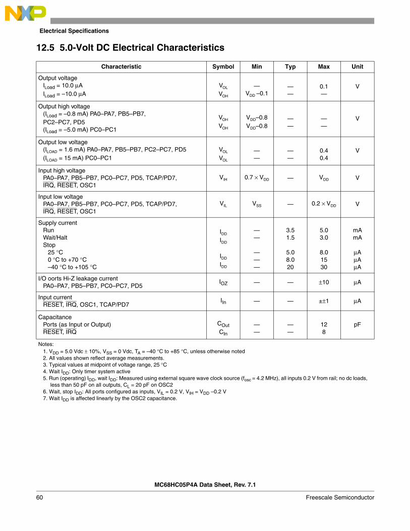
Electrical Specifications
MC68HC05P4A Data Sheet, Rev. 7.1
60 Freescale Semiconductor
12.5 5.0-Volt DC Electrical Characteristics
Characteristic Symbol Min Typ Max Unit
Output voltageILoad = 10.0 µAILoad = –10.0 µA
VOL
VOH
—VDD –0.1
——
0.1—
V
Output high voltage(ILoad = –0.8 mA) PA0–PA7, PB5–PB7, PC2–PC7, PD5(ILoad = –5.0 mA) PC0–PC1
VOH
VOH
VDD–0.8VDD–0.8
——
——
V
Output low voltage(ILOAD = 1.6 mA) PA0–PA7, PB5–PB7, PC2–PC7, PD5(ILOAD = 15 mA) PC0–PC1
VOL
VOL
——
——
0.40.4
V
Input high voltagePA0–PA7, PB5–PB7, PC0–PC7, PD5, TCAP/PD7,IRQ, RESET, OSC1
VIH 0.7 × VDD — VDD V
Input low voltagePA0–PA7, PB5–PB7, PC0–PC7, PD5, TCAP/PD7,IRQ, RESET, OSC1
VIL VSS — 0.2 × VDD V
Supply currentRun Wait/Halt Stop
25 °C0 °C to +70 °C –40 °C to +105 °C
IDD
IDD
IDD
IDD
——
———
3.51.5
5.08.020
5.03.0
8.01530
mAmA
µAµAµA
I/O oorts Hi-Z leakage currentPA0–PA7, PB5–PB7, PC0–PC7, PD5
IOZ — — ±10 µA
Input currentRESET, IRQ, OSC1, TCAP/PD7
IIn — — ±±1 µA
CapacitancePorts (as Input or Output)RESET, IRQ
COut
CIn
——
——
128
pF
Notes:1. VDD = 5.0 Vdc ± 10%, VSS = 0 Vdc, TA = –40 °C to +85 °C, unless otherwise noted2. All values shown reflect average measurements.3. Typical values at midpoint of voltage range, 25 °C4. Wait IDD: Only timer system active5. Run (operating) IDD, wait IDD: Measured using external square wave clock source (fosc = 4.2 MHz), all inputs 0.2 V from rail; no dc loads,
less than 50 pF on all outputs, CL = 20 pF on OSC26. Wait, stop IDD: All ports configured as inputs, VIL = 0.2 V, VIH = VDD –0.2 V7. Wait IDD is affected linearly by the OSC2 capacitance.
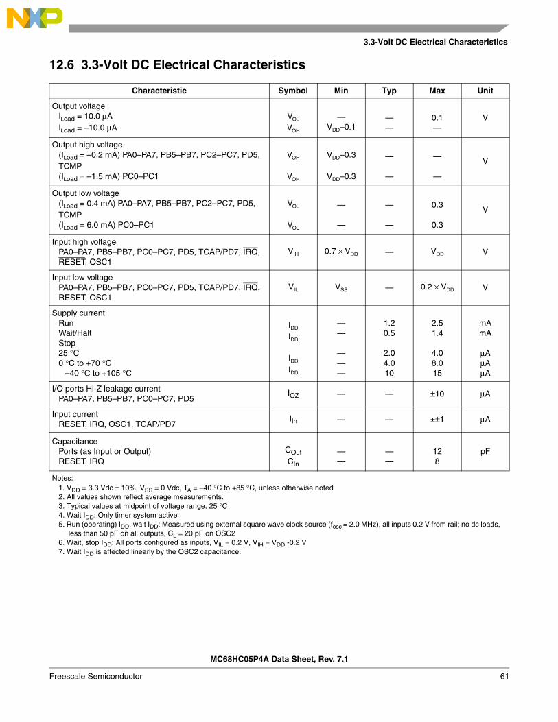
3.3-Volt DC Electrical Characteristics
MC68HC05P4A Data Sheet, Rev. 7.1
Freescale Semiconductor 61
12.6 3.3-Volt DC Electrical Characteristics
Characteristic Symbol Min Typ Max Unit
Output voltageILoad = 10.0 µAILoad = –10.0 µA
VOL
VOH
—VDD–0.1
——
0.1—
V
Output high voltage(ILoad = –0.2 mA) PA0–PA7, PB5–PB7, PC2–PC7, PD5, TCMP(ILoad = –1.5 mA) PC0–PC1
VOH
VOH
VDD–0.3
VDD–0.3
—
—
—
—
V
Output low voltage(ILoad = 0.4 mA) PA0–PA7, PB5–PB7, PC2–PC7, PD5, TCMP(ILoad = 6.0 mA) PC0–PC1
VOL
VOL
—
—
—
—
0.3
0.3
V
Input high voltagePA0–PA7, PB5–PB7, PC0–PC7, PD5, TCAP/PD7, IRQ, RESET, OSC1
VIH 0.7 × VDD — VDD V
Input low voltagePA0–PA7, PB5–PB7, PC0–PC7, PD5, TCAP/PD7, IRQ, RESET, OSC1
VIL VSS — 0.2 × VDD V
Supply currentRun Wait/Halt Stop25 °C0 °C to +70 °C
–40 °C to +105 °C
IDD
IDD
IDD
IDD
——
———
1.20.5
2.04.010
2.51.4
4.08.015
mAmA
µAµAµA
I/O ports Hi-Z leakage currentPA0–PA7, PB5–PB7, PC0–PC7, PD5
IOZ — — ±10 µA
Input currentRESET, IRQ, OSC1, TCAP/PD7
IIn — — ±±1 µA
CapacitancePorts (as Input or Output)RESET, IRQ
COutCIn
——
——
128
pF
Notes:1. VDD = 3.3 Vdc ± 10%, VSS = 0 Vdc, TA = –40 °C to +85 °C, unless otherwise noted2. All values shown reflect average measurements.3. Typical values at midpoint of voltage range, 25 °C4. Wait IDD: Only timer system active5. Run (operating) IDD, wait IDD: Measured using external square wave clock source (fosc = 2.0 MHz), all inputs 0.2 V from rail; no dc loads,
less than 50 pF on all outputs, CL = 20 pF on OSC26. Wait, stop IDD: All ports configured as inputs, VIL = 0.2 V, VIH = VDD -0.2 V 7. Wait IDD is affected linearly by the OSC2 capacitance.
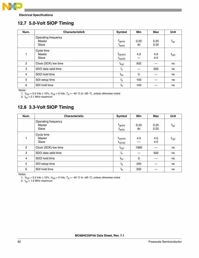
Electrical Specifications
MC68HC05P4A Data Sheet, Rev. 7.1
62 Freescale Semiconductor
12.7 5.0-Volt SIOP Timing
12.8 3.3-Volt SIOP Timing
Num. Characteristic6 Symbol Min Max Unit
Operating frequencyMasterSlave
fop(m)fop(s)
0.25dc
0.250.25
fop
1Cycle time
MasterSlave
tcyc(m)tcyc(s)
4.0—
4.04.0
tcyc
2 Clock (SCK) low time tcyc 932 — ns
3 SDO data valid time tv — 200 ns
4 SDO hold time tho 0 — ns
5 SDI setup time ts 100 — ns
6 SDI hold time th 100 — ns
Notes: 1. VDD = 5.0 Vdc ± 10%, VSS = 0 Vdc, TA = –40 °C to +85 °C, unless otherwise noted2. fop = 2.1 MHz maximum
Num. Characteristic Symbol Min Max Unit
Operating frequencyMasterSlave
fop(m)fop(s)
0.25dc
0.250.25
fop
1Cycle time
MasterSlave
tcyc(m)
tcyc(s)
4.0—
4.04.0
tcyc
2 Clock (SCK) low time tcyc 1980 — ns
3 SDO data valid time tv — 400 ns
4 SDO hold time tho 0 — ns
5 SDI setup time ts 200 — ns
6 SDI hold time th 200 — ns
Notes: 1. VDD = 3.3 Vdc ± 10%, VSS = 0 Vdc, TA = –40 °C to +85 °C, unless otherwise noted2. fop = 1.0 MHz maximum
5.0-Volt Control Timing
MC68HC05P4A Data Sheet, Rev. 7.1
Freescale Semiconductor 63
Figure 12-1. SIOP Timing Diagram
12.9 5.0-Volt Control Timing
Characteristic Symbol Min Max Unit
Frequency of operationCrystal optionExternal clock option
fosc —dc
4.24.2
MHz
Internal operating frequencyCrystal (fosc ÷ 2)External Clock (fosc ÷ 2)
fop —dc
2.12.1
MHz
Cycle time tcyc 480 — ns
Crystal oscillator startup time tOXOV — 100 ms
Stop recovery startup time (crystal oscillator) tILCH — 100 ms
RESET pulse width tRL 1.5 — tcyc
Interrupt pulse width low (edge-triggered) tILIH 125 — ns
Interrupt pulse period tILIL * — tcyc
OSC1 pulse width tOH, tOL 90 — ns
Note:1. VDD = 5.0 Vdc ± 10%, VSS = 0 Vdc, TA = –40 °C to +85 °C, unless otherwise noted
*The minimum period tILIL should not be less than the number of cycles it takes to execute the interrupt service routine plus 19 tcyc.
SDO BIT 0 BIT 1 BIT 6
SCK
BIT 7
SDI BIT 0 BIT 1 BIT 6
BIT 7
1
2
3 4
5
6
Electrical Specifications
MC68HC05P4A Data Sheet, Rev. 7.1
64 Freescale Semiconductor
12.10 3.3-Volt Control Timing
Figure 12-2. STOP Recovery Timing
Characteristic Symbol Min Max Unit
Frequency of operationCrystal OptionExternal Clock Option
fosc —dc
2.02.0
MHz
Internal operating frequencyCrystal (fosc ÷ 2)External clock (fosc ÷ 2)
fop —dc
1.01.0
MHz
Cycle time tcyc 1000 — ns
Crystal oscillator startup time tOXOV — 100 ms
Stop recovery startup time (crystal oscillator) tILCH — 100 ms
RESET pulse width, excluding powerup tRL 1.5 — tcyc
Interrupt pulse width low (edge-triggered) tILIH 250 — ns
Interrupt pulse period tILIL * — tcyc
OSC1 pulse width tOH, tOL 200 — ns
Notes:1. VDD = 3.3 Vdc ± 10%, VSS = 0 Vdc, TA = –40°C to +85°C, unless otherwise noted
*The minimum period tILIL should not be less than the number of cycles it takes to execute the interrupt service routine plus 19 tcyc.
1FFF1FFE1FFE1FFE1FFE1FFE 4
RESET OR INTERRUPTVECTOR FETCH
INTERNALCLOCK
IRQ 3
OSC 1
IRQ 2
INTERNALADDRESS
BUS
RESET
Notes: 1. Represents the internal clocking of the OSC1 pin. 2. IRQ pin edge-sensitive mask option 3. IRQ pin level- and edge-sensitive mask option 4. RESET vector address shown for timing example
tRL
t ILIH
4064 tcyc
3.3-Volt Control Timing
MC68HC05P4A Data Sheet, Rev. 7.1
Freescale Semiconductor 65
Figure 12-3. External Interrupt Timing
Figure 12-4. Power-On Reset Timing
•••
ILIHt
ILILt
ILIHtIRQ (PIN)
IRQn
IRQ1
RQ (MCU)
NORMALLYUSED WITHWIRE-ORedCONNECTION
Edge-Sensitive Trigger ConditionThe minimum pulse width (tILIH) is either125 ns (VDD = 5 V) or 250 ns (VDD = 3 V).The period tILIL should not be less thanthe number of tcyc cycles it takes toexecute the interrupt service routineplus 19 tcyc cycles.
Level-Sensitive Trigger ConditionIf after servicing an interrupt the IRQremains low, then the next interrupt isrecognized.
SC1 PIN
VDD
4064 tcyc
INTERNALCLOCK
INTERNALADDRESS
BUS
INTERNALDATA
BUS
1FFF1FFE1FFE1FFE1FFE
NEWPCL
NEWPCH
1FFE1FFE
VDD THRESHOLD (TYPICALLY 1-2 V)
t VDDR
Notes:1. Internal clock, internal address bus, and internal data bus signals are not available externally.2. An internal POR reset is triggered as VDD rises through a threshold (typically 1–2 V).
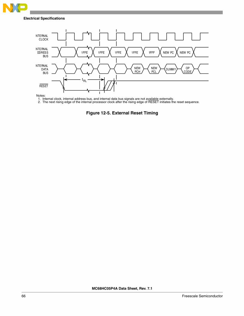
Electrical Specifications
MC68HC05P4A Data Sheet, Rev. 7.1
66 Freescale Semiconductor
Figure 12-5. External Reset Timing
NTERNALCLOCK
NTERNALDDRESS
BUS
RESET
tRL
NEW PC
DUMMYNTERNAL
DATABUS
NEW PC
OPCODE
1FFF
NEWPCL
1FFE
NEWPCH
1FFE1FFE1FFE
Notes:1. Internal clock, internal address bus, and internal data bus signals are not available externally.2. The next rising edge of the internal processor clock after the rising edge of RESET initiates the reset sequence.
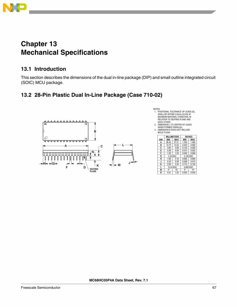
MC68HC05P4A Data Sheet, Rev. 7.1
Freescale Semiconductor 67
Chapter 13 Mechanical Specifications
13.1 Introduction
This section describes the dimensions of the dual in-line package (DIP) and small outline integrated circuit (SOIC) MCU package.
13.2 28-Pin Plastic Dual In-Line Package (Case 710-02)
°
°
°
°
!"!#! ! $
! !
! #!
1 14
1528
B
A C
N
K MJ
D
FH G
L
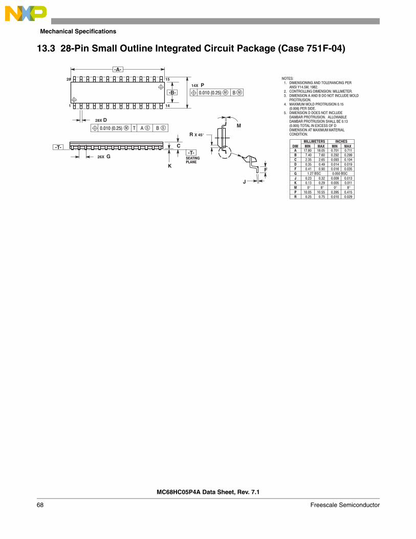
Mechanical Specifications
MC68HC05P4A Data Sheet, Rev. 7.1
68 Freescale Semiconductor
13.3 28-Pin Small Outline Integrated Circuit Package (Case 751F-04)
°
°
°
°
!$ $
%! $ ! !! ! # !
# !"!#! ! #
! #
! # ! # " ! !"!#! !
-A-
-B-
1 14
1528
-T- C
! !
M
J
-T-
K
26X G
28X D
14X P
R X 45°
F
!
MC68HC05P4A Data Sheet, Rev. 7.1
Freescale Semiconductor 69
Chapter 14 Ordering Information
14.1 Introduction
This section contains instructions for ordering custom-masked ROM MCUs.
14.2 MCU Ordering Forms
To initiate an order for a ROM-based MCU, first obtain the current ordering form for the MCU from a Freescale representative. Submit the following items when ordering MCUs:
• A current MCU ordering form that is completely filled out (Contact your Freescale sales office for assistance.)
• A copy of the customer specification if the customer specification deviates from the Freescale specification for the MCU
• Customer’s application program on one of the media listed in 14.3 Application Program Media
14.3 Application Program Media
Deliver the application program to Freescale in one of the following media:• Macintosh®(1) 3 1/2-inch diskette (double-sided 800 K or double-sided high-density 1.4 M)• MS-DOS®(2) or PC-DOSTM(3) 3 1/2-inch diskette (double-sided 720 K or double-sided high-density
1.44 M)• MS-DOS® or PC-DOSTM 5 1/4-inch diskette (double-sided double- density 360 K or double-sided
high-density 1.2 M)
Use positive logic for data and addresses.
When submitting the application program on a diskette, clearly label the diskette with the following information:
• Customer name• Customer part number• Project or product name• File name of object code• Date• Name of operating system that formatted diskette• Formatted capacity of diskette
1. Macintosh is a registered trademark of Apple Computer, Inc.2. MS-DOS is a registered trademark of Microsoft Corporation.3. PC-DOS is a trademark of International Business Machines Corporation.
Ordering Information
MC68HC05P4A Data Sheet, Rev. 7.1
70 Freescale Semiconductor
On diskettes, the application program must be in Freescale’s S-record format (S1 and S9 records), a character-based object file format generated by M6805 cross assemblers and linkers.
NOTEBegin the application program at the first user ROM location. Program addresses must correspond exactly to the available on-chip user ROM addresses as shown in the memory map. Write $00 in all non-user ROM locations or leave all non-user ROM locations blank. Refer to the current MCU ordering form for additional requirements. Freescale may request pattern re-submission if non-user areas contain any non-zero code.
If the memory map has two user ROM areas with the same address, then write the two areas in separate files on the diskette. Label the diskette with both file names.
In addition to the object code, a file containing the source code can be included. Freescale keeps this code private and uses it only to expedite ROM pattern generation in case of any difficulty with the object code. Label the diskette with the file name of the source code.
14.4 ROM Program Verification
The primary use for the on-chip ROM is to hold the customer’s application program. The customer develops and debugs the application program and then submits the MCU order along with the application program.
Freescale inputs the customer’s application program code into a computer program that generates a listing verify file. The listing verify file represents the memory map of the MCU. The listing verify file contains the user ROM code and may also contain non-user ROM code, such as self-check code. Freescale sends the customer a computer printout of the listing verify file along with a listing verify form.
To aid the customer in checking the listing verify file, Freescale will program the listing verify file into customer-supplied blank preformatted Macintosh or DOS disks. All original pattern media are filed for contractual purposes and are not returned.
Check the listing verify file thoroughly, then complete and sign the listing verify form, and return the listing verify form to Freescale. The signed listing verify form constitutes the contractual agreement for the creation of the custom mask.
14.5 ROM Verification Units (RVUs)
After receiving the signed listing verify form, Freescale manufactures a custom photographic mask. The mask contains the customer’s application program and is used to process silicon wafers. The application program cannot be changed after the manufacture of the mask begins. Freescale then produces 10 MCUs, called RVUs, and sends the RVUs to the customer. RVUs are usually packaged in unmarked ceramic and tested to 5 Vdc at room temperature. RVUs are not tested to environmental extremes because their sole purpose is to demonstrate that the customer’s user ROM pattern was properly implemented. The 10 RVUs are free of charge with the minimum order quantity. These units are not to be used for qualification or production. RVUs are not guaranteed by Freescale Quality Assurance.

blank
How to Reach Us:
Home Page:www.freescale.com
E-mail:[email protected]
USA/Europe or Locations Not Listed:Freescale SemiconductorTechnical Information Center, CH3701300 N. Alma School RoadChandler, Arizona 85224+1-800-521-6274 or [email protected]
Europe, Middle East, and Africa:Freescale Halbleiter Deutschland GmbHTechnical Information CenterSchatzbogen 781829 Muenchen, Germany+44 1296 380 456 (English)+46 8 52200080 (English)+49 89 92103 559 (German)+33 1 69 35 48 48 (French)[email protected]
Japan:Freescale Semiconductor Japan Ltd.HeadquartersARCO Tower 15F1-8-1, Shimo-Meguro, Meguro-ku,Tokyo 153-0064Japan0120 191014 or +81 3 5437 [email protected]
Asia/Pacific:Freescale Semiconductor Hong Kong Ltd.Technical Information Center2 Dai King StreetTai Po Industrial EstateTai Po, N.T., Hong Kong+800 2666 [email protected]
For Literature Requests Only:Freescale Semiconductor Literature Distribution CenterP.O. Box 5405Denver, Colorado 802171-800-441-2447 or 303-675-2140Fax: [email protected]
Information in this document is provided solely to enable system and software implementers to use Freescale Semiconductor products. There are no express or implied copyright licenses granted hereunder to design or fabricate any integrated circuits or integrated circuits based on the information in this document.
Freescale Semiconductor reserves the right to make changes without further notice to any products herein. Freescale Semiconductor makes no warranty, representation or guarantee regarding the suitability of its products for any particular purpose, nor does Freescale Semiconductor assume any liability arising out of the application or use of any product or circuit, and specifically disclaims any and all liability, including without limitation consequential or incidental damages. “Typical” parameters that may be provided in Freescale Semiconductor data sheets and/or specifications can and do vary in different applications and actual performance may vary over time. All operating parameters, including “Typicals”, must be validated for each customer application by customer’s technical experts. Freescale Semiconductor does not convey any license under its patent rights nor the rights of others. Freescale Semiconductor products are not designed, intended, or authorized for use as components in systems intended for surgical implant into the body, or other applications intended to support or sustain life, or for any other application in which the failure of the Freescale Semiconductor product could create a situation where personal injury or death may occur. Should Buyer purchase or use Freescale Semiconductor products for any such unintended or unauthorized application, Buyer shall indemnify and hold Freescale Semiconductor and its officers, employees, subsidiaries, affiliates, and distributors harmless against all claims, costs, damages, and expenses, and reasonable attorney fees arising out of, directly or indirectly, any claim of personal injury or death associated with such unintended or unauthorized use, even if such claim alleges that Freescale Semiconductor was negligent regarding the design or manufacture of the part.
Freescale™ and the Freescale logo are trademarks of Freescale Semiconductor, Inc.All other product or service names are the property of their respective owners.© Freescale Semiconductor, Inc. 2005. All rights reserved.
MC68HC05P4ARev. 7.1, 9/2005
RXZB30
rohstext
Related Documents