Ordering Information Device Temp Range Package MC44BS374CAD,R2 0°C to +70°C SO16NB MC44BS374CAEF,R2 0°C to +70°C SO16NB Lead free NOTE: For tape and reel, add R2 suffix. SO16NB Package This document contains information on a product under development. Freescale reserves the right to change or discontinue this product without notice. © Motorola, Inc., 2003. All rights reserved. MC44BS374CA The MC44BS374CA audio and video modulator is for use in VCRs, set-top boxes, and similar devices. • Multi standard • TV output level 82dBuV typical • 5V and 3.3V compatible I 2 C bus Figure 1 shows the pin connections. Figure 1. MC44BS374CA Pin Connections GNDD VCCD XTAL GND TVOVCC AUDIO GND PLLFLT SDA SCL LOP PREEM TVOUT VCCA 1 2 3 4 5 6 7 8 16 15 14 13 12 11 10 9 SPLFLT VIDEO SO16 pin package Technical data MC44BS374CA Rev. 1.2 04/2004 PLL Tuned UHF and VHF Audio/Video High Integration Modulator Contents Features . . . . . . . . . . . . . . . 2 Comparing the MC44BS374CA to the MC44BC374C . . . . . . . . 3 Pin Descriptions . . . . . . . . 3 MC44BS374CA Functional Overview . . . . . . . . . . . . 4 Maximum Ratings . . . . . . . 5 Thermal Ratings . . . . . . . . . 5 Electrostatic Discharge . . . 5 Electrical Characteristics . 6 I2C Bit Mapping . . . . . . . . . 7 I2C Programming . . . . . . . . 8 Modulator High Frequency Characteristics . . . . . . 10 Video Characteristics . . . 11 Audio Characteristics . . . 13 Characterization Measurement Conditions 14 MC44BS374CA Modes of Operation . . . . . . . . . . . 20 High Speed I2C Compatible Bus . . . . . . . . . . . . . . . . 24 Pin Circuit Schematics . . 27 Application Diagram . . . . 28 MC44BS374CA Evaluation Board Layout and Schematic . . . . . . . . . . 29 Packaging Instructions . . 31 Marking Instructions . . . . 31 Case Outline 32 Freescale S emiconduct or, I Freescale Semiconductor, Inc. For More Information On This Product, Go to: www.freescale.com nc...

Welcome message from author
This document is posted to help you gain knowledge. Please leave a comment to let me know what you think about it! Share it to your friends and learn new things together.
Transcript

Ordering Information
Device Temp Range Package
MC44BS374CAD,R2 0°C to +70°C SO16NB
MC44BS374CAEF,R2 0°C to +70°C SO16NBLead free
NOTE: For tape and reel, add R2 suffix.
SO16NB Package
This document contains information on a product under development. Freescale reserves the right to change or discontinue this product without notice. © Motorola, Inc., 2003. All rights reserved.
MC44BS374CA
The MC44BS374CA audio and video modulator is for use in VCRs, set-top boxes, and similar devices.
• Multi standard• TV output level 82dBuV typical
• 5V and 3.3V compatible I2C bus
Figure 1 shows the pin connections.
Figure 1. MC44BS374CA Pin Connections
GNDD
VCCD
XTAL
GND
TVOVCC
AUDIO
GND
PLLFLTSDA
SCL
LOP
PREEM
TVOUT
VCCA
1
2
3
4
5
6
7
8
1615
14
13
12
11
10
9SPLFLT VIDEO
SO16 pin package
Technical data
MC44BS374CA Rev. 1.2 04/2004
PLL Tuned UHF and VHF Audio/Video High Integration Modulator
ContentsFeatures . . . . . . . . . . . . . . . 2Comparing the
MC44BS374CA to the MC44BC374C . . . . . . . . 3
Pin Descriptions . . . . . . . . 3MC44BS374CA Functional
Overview . . . . . . . . . . . . 4Maximum Ratings . . . . . . . 5Thermal Ratings . . . . . . . . . 5Electrostatic Discharge . . . 5Electrical Characteristics . 6I2C Bit Mapping . . . . . . . . . 7I2C Programming . . . . . . . . 8Modulator High Frequency
Characteristics . . . . . . 10Video Characteristics . . . 11Audio Characteristics . . . 13Characterization
Measurement Conditions 14
MC44BS374CA Modes of Operation . . . . . . . . . . . 20
High Speed I2C Compatible Bus . . . . . . . . . . . . . . . . 24
Pin Circuit Schematics . . 27Application Diagram . . . . 28MC44BS374CA Evaluation
Board Layout and Schematic . . . . . . . . . . 29
Packaging Instructions . . 31Marking Instructions . . . . 31Case Outline 32
Fre
esc
ale
Se
mic
on
du
cto
r, I
Freescale Semiconductor, Inc.
For More Information On This Product, Go to: www.freescale.com
nc
...
RXZB30
logo

MC44BS374CA Technical data
Features
1 FeaturesThe MC44BS374CA is a Multi-Standard, PAL/NTSC Modulator.
The channel is set by an on-chip high-speed I2C compatible bus receiver. A Phase-Locked Loop ( PLL ) tunes the modulator over the full UHF range.
The modulator incorporates a sound subcarrier oscillator and uses a second PLL to derive 4.5, 5.5, 6.0, and 6.5 MHz subcarrier frequencies. These frequencies are selectable by bus.
The picture-to-sound ratio may be adjusted using the bus. In addition, an on-chip video test pattern generator can be switched ON with a 1 KHz audio test signal.
The MC44BS374CA also has the following features:
• Integrated on-chip programmable UHF oscillator• No external varicaps diodes / inductor or tuned components• Extremely low external components count• Channel 21-69 UHF operation• VHF range possible by internal dividers (30MHz-450MHz)• Boosted TVout level (82 dBuV typical)
• High speed read and write I2C-bus compatible (800kHz)
• I2C-bus 5V and 3.3V compatible • Fixed video modulation depth (82% typical)• Peak White Clip disabled by bus• Programmable picture/sound carrier ratio (12dB and 16dB)• Integrated on-chip programmable sound subcarrier oscillator (4.5, 5.5, 6.0 and 6.5 MHz) - No
external varicaps• On-chip video test pattern generator with sound test signal (1kHz)• Low-power programmable modulator standby mode• Transient output inhibit during PLL Lock-up at power-ON• Logical Output Port controlled by bus• ESD protection, minimum 4 kV
Fre
esc
ale
Se
mic
on
du
cto
r, I
Freescale Semiconductor, Inc.
For More Information On This Product, Go to: www.freescale.com
nc
...

Comparing the MC44BS374CA to the MC44BC374C
MC44BS374CA Technical data
2 Comparing the MC44BS374CA to the MC44BC374CCompared to the MC44BC374C devices, the MC44BS374CA has the following improvements:
• Higher output level (82 dBuV versus 74.5 dBuV)• Higher Video signal to noise (+ 3 dB)
• I2C-bus 3.3V compatible• Lower power consumption in normal and standby modes (-2 mA)
• The device can be powered down without holding the I2C lines down.• TB1 bit is no more available (limited compatibility with MC44355 devices no more available)• Switch between the two integrated VCO’s controlled directly by the frequency divider (@ 700
MHz)
3 Pin DescriptionsTable 1. Package Pin Descriptions
Pin number Pin Name Description
1 SCL I2C clock
2 SDA I2C data
3 LOP Logical output port controlled by I2C bus
4 XTAL Crystal
5 GND Ground
6 PREEMP Pre-emphasis capacitor
7 AUDIO Audio input
8 SPLFLT Sound PLL loop filter
9 VIDEO Video input
10 VCCA Main analog supply voltage
11 GND Analog ground
12 TVOUT TV output signal
13 TVOVCC TV output stage supply voltage
14 PLLFLT RF PLL loop filter
15 VCCD Digital supply voltage
16 GNDD Digital ground
Fre
esc
ale
Se
mic
on
du
cto
r, I
Freescale Semiconductor, Inc.
For More Information On This Product, Go to: www.freescale.com
nc
...

MC44BS374CA Technical data
MC44BS374CA Functional Overview
4 MC44BS374CA Functional OverviewFigure 2 shows a simplified block diagram of the MC44BS374CA device.
The MC44BS374CA device has three main sections:
1. A high speed I2C-compatible bus section2. A PLL section to synthesize the UHF / VHF output channel frequency (from an integrated
UHF oscillator, divided for VHF output)3. A modulator section, which accepts audio and video inputs, then uses them to modulate the
UHF/VHF carrier
An on-chip video test pattern generator with an audio test signal is included.
The MC44BS374CA operates as a multi-standard modulator and can handle the following systems using the same external circuit components: B / G, I, D / K, M / N.
High frequency BiCMOS technology allows integration of the UHF tank circuit and certain filtering functions.
Figure 2. MC44BS374CA Simplified Block Diagram
8
13
1
2
6
11
14
9
4
12
7
3
10
15 16
TVOVCC
TVOUT
LOP VIDEO SPLLFLT
AUDIO
VCCA
GND
PREEM
XTALPLLFLTGNDDVCCD
SCL
SDA
BUS SECTION VCO and PLL SECTION
MODULATORSECTIONClamp
PeakWhite
31.25KHz
4MHzXCO
Ref Divider/128
PhaseComp
PLL
ProgDivider
Prescaler/8
VHF Dividers
VideoModulator
LPF
LPF
RF SoundModulator
FM
ALCLPFProgDivider
AudioAmplifier
SoundOscillatorand FM
Modulator
SoundPFD
High SpeedI2C BusReceiver
UHF OSC
I 2C BU
SI 2C
BUS
I2C BUS
I2C BUS
I 2C BU
S
75Ω
5 GND
Clip
31.25KHz
Fre
esc
ale
Se
mic
on
du
cto
r, I
Freescale Semiconductor, Inc.
For More Information On This Product, Go to: www.freescale.com
nc
...

Maximum Ratings
MC44BS374CA Technical data
5 Maximum Ratings
6 Thermal Ratings
7 Electrostatic DischargeElectrostatic Discharge ( ESD ) tests are done on all pins
Sym Parameter Value Unit
Rthja Thermal resistance from Junction to Ambient 102 °C/W
Sym Parameter Min Unit
ESD MM (Machine Model) - MIL STD 883C method 3015-7 400 VESD HBM (Human Body Model) - MIL STD 883C method 3015-7 4000 V
Sym Parameter Value Unit
Vcc Supply voltage 6 V
Tamin Minimum operating ambient temperature 0 oC
Tamax Maximum operating ambient temperature +70 oC
Tstgmin Minimum storage temperature -65 oC
Tstgmax Maximum storage temperature 150 oC
Tj Junction Temperature 150 oC
This device contains protection circuitry to guard
against damage due to high static voltage or electric
fields. However, precautions must be taken to avoid
applications of any voltage higher than maximum rated
voltages to this high impedance circuit. For proper
operation, input and output voltages should be
constrained to the ranges indicated in the
Recommended Operating Conditions.
Note: Maximum ratings are those values beyond which damage to the device may occur. For functional operation, values should be restricted to the Recommended Operating Condition.Note: Meets Moisture Sensitivity Level 1, no dry pack required.
Fre
esc
ale
Se
mic
on
du
cto
r, I
Freescale Semiconductor, Inc.
For More Information On This Product, Go to: www.freescale.com
nc
...

MC44BS374CA Technical data
Electrical Characteristics
8 Electrical Characteristics• A = 100% tested• B = 100% Correlation tested• C = Characterized on samples• D = Design parameter
See Characterization conditions section for each C type parameter.
8.1 Operating ConditionsUnless otherwise stated: Vcc=5.0 V, Ambient Temperture=25o C, Video Input 1Vp-p, 10-step grayscale. RF output into 75 Ohm load.
NOTE:Specifications only valid for envelope demodulation.
Table 2. Operating Conditions
Parameter Min Typ Max Unit Notes Type
Operating supply voltage range 4.5 5.0 5.5 V B
Total supply current 42 50 58 mA All sections active A
Total standby mode supply current 3 5 7 mA OSC, SO, ATT = 1 Bus Section active A
Test pattern sync pulse width 3 4.7 6.5 µS B
Sound comparator charge pump current During locking When locked
70.7
101
121.5
µAµA
AA
RF comparator charge pump current 60 100 150 µA A
Crystal oscillator stability-negative resistance 1 - - K Ω D
Logic Output Port Saturation voltage at I = 2 mA Leakage current
--
160-
3001
mVµA
AA
Fre
esc
ale
Se
mic
on
du
cto
r, I
Freescale Semiconductor, Inc.
For More Information On This Product, Go to: www.freescale.com
nc
...

I2C Bit Mapping
MC44BS374CA Technical data
9 I2C Bit MappingWRITE MODE Bit 7 Bit 6 Bit 5 Bit 4 Bit 3 Bit 2 Bit 1 Bit 0 ACK
CA-CHIP ADDRESS 1 1 0 0 1 0 1 0 ACK
C1-High Order Bits 1 0 SO LOP PS X3 X2 0 ACK
C0-Low Order Bits PWC OSC ATT SFD1 SFD0 0 X5 X4 ACK
FM-High Order Bits 0 TPEN N11 N10 N9 N8 N7 N6 ACK
FL-Low Order Bits N5 N4 N3 N2 N1 N0 X1 X0 ACK
READ MODE Bit 7 Bit 6 Bit 5 Bit 4 Bit 3 Bit 2 Bit 1 Bit 0 ACK
CHIP ADDRESS 1 1 0 0 1 0 1 1 ACK
R-Status Byte - - - - - Y2 Y1 OOR -
Bit Name Description
PWC Peak White Clip enable / disable
OSC UHF oscillator ON / OFF
ATT Modulator output attenuated-sound and video modulators ON / OFF
SFD0, 1 Sound subcarrier frequency control bits
SO Sound Oscillator ON / OFF
LOP Logic Output Port
PS Picture-to-sound carrier ratio
TPEN Test pattern enable-picture and sound
X5…X0 Test mode bits-All bits are 0 for normal operation (see Test Mode tables, page 6 & page 7)
N0…N11 UHF frequency programming bits, in steps of 250 kHz
OOR RF oscillator out-of-frequency range information
Y1, Y2 RF oscillator operating range information
Fre
esc
ale
Se
mic
on
du
cto
r, I
Freescale Semiconductor, Inc.
For More Information On This Product, Go to: www.freescale.com
nc
...

MC44BS374CA Technical data
I2C Programming
10 I2C Programming
WRITE MODE: Test Mode 1 and VHF Range
X2 X1 X0 State Description
0 0 0 1.a Normal operation
0 0 1 1.b RF frequency divided for low frequency testing or VHF range: RF / 2
0 1 0 1.c RF / 4
0 1 1 1.d RF / 8
1 0 0 1.e RF / 16
1 0 1 1.f DC drive applied to modulators: Non-inverted video at TVOUT
1 1 0 1.g DC drive applied to modulators: Inverted video at TVOUT
1 1 1 1.hTransient output inhibit disabled (ie speed up mode)During this speed-up test mode, ATT=0 forces sound current source to 1µA, and ATT=1 forces it to 10µA.
Sound
Video
SFD 1 SFD 0 Sound Subcarrier Freq (MHz)
0 0 4.5
0 1 5.5
1 0 6.0
1 1 6.5
PS Picture-to-Sound Ratio (dB)
0 12
1 16
SO Sound Oscillator
0 Sound oscillator ON (Normal mode)
1 Sound oscillation disabled (oscillator and PLL section bias turned OFF)
PWC Peak White Clip
0 Peak White Clip ON (System B / G)
1 Peak White Clip OFF (System L)
TPEN Test Pattern Signal
0 Test pattern signal OFF (normal operation)
1 Test pattern signal ON (picture and sound)
UHF
Standby Mode
Logic Output Port
OSC UHF Oscillator
0 Normal operation
1 UHF oscillator disabled (oscillator and PLL sections bias turned OFF)
ATT Modulator Output Attenuation
0 Normal operation
1 Modulator output attenuation (sound and video modulators sections bias turned OFF.
OSC SO ATT Combination of 3-bits
1 1 1 Modulator standby mode
LOP Description
0 Pin 3 is low voltage
1 Pin 3 is high impedance
Fre
esc
ale
Se
mic
on
du
cto
r, I
Freescale Semiconductor, Inc.
For More Information On This Product, Go to: www.freescale.com
nc
...

I2C Programming
MC44BS374CA Technical data
WRITE MODE: Test Mode 2
NOTE:Test modes 1 and 2 are intended for manufacturing test purposes only and cannot be used for normal applications, except for VHF range (states 1.b to 1.e).
READ MODE
X5 X4 X3 State Description
0 0 0 2.a Normal operation
0 0 1 2.b Test pattern generator DC verification (Test pattern DC test mode available)
0 1 0 2.c Program divider test (UHF program divider on PLLFILT pin and sound program divider on SPLLFIL pin)
0 1 1 2.d Reference divider test (UHF reference divider on PLLFILT pin)
1 0 0 2.eUHF phase comparison, upper source on PLLFILT pin Sound phase comparison 10 µA upper source on SPLLFIL ( Only valid during transient output inhibit. )
1 0 1 2.fUHF phase comparison, lower source on PLLFILT pin Sound phase comparison 10 µA lower source on SPLLFIL ( Only valid during transient output inhibit. )
1 1 0 2.g Sound phase comparison 1 µA upper source on SPLLFIL ( Not valid during transient output inhibit. )
1 1 1 2.h Sound phase comparison 1 µA lower source on SPLLFIL ( Not valid during transient output inhibit. )
OOR Description
0 Normal operation, VCO in range
1 VCO out of range
Y1 Description
0 VCO out of range, frequency too low, only valid if OOR=1
1 VCO out of range, frequency too high, only valid if OOR=1
Y2 Description
0 High VCO is active
1 Low VCO is active
Fre
esc
ale
Se
mic
on
du
cto
r, I
Freescale Semiconductor, Inc.
For More Information On This Product, Go to: www.freescale.com
nc
...

MC44BS374CA Technical data
Modulator High Frequency Characteristics
11 Modulator High Frequency CharacteristicsUnless otherwise stated: Vcc=5.0 V, Ambient Temperture=25o C, Video Input 1Vp-p, 10-step grayscale. RF inputs / outputs into 75 Ohm load.
NOTE:Specifications only valid for envelope demodulation.
Table 3. High Frequency Characteristics
Parameter Test Conditions Min Typ Max Unit Type
TVOUT output level Output signal from modulator sectionSee Figure 3. See Note 2 79 82 85 dBµV B
UHF oscillator frequency 460 - 880 MHz A
VHF range From UHF oscillator internally divided 45 - 460 MHz B
TVOUT output attenuation
During transient output inhibit, or when ATT bit is set to 1. See Figure 3. See Note 2
65 75 - dBc B
Sound subcarrier harmonics (Fp + n ∗ Fs) Reference picture carrier. See Note 2 50 63 - dBc C
Second harmonic of chroma subcarrier Using red EBU bar. See Note 2 45 70 - dBc C
Chroma / Sound intermodulation: Fp + ( Fsnd - Fchr ) Using red EBU bar.See Note 2 65 82 - dBc C
Fo (picture carrier) harmonics
2nd harmonic: CH21 3rd harmonic: CH21 Other channels: See Figure 3. See NOTE 1. See Note 2
--
3858
5070 dBµV C
Out band (picture carrier) spurious
1 / 2 ∗ Fo - 1 / 4 ∗ Fo - 3 / 2 ∗ Fo - 3 / 4 ∗ Fo From 40 MHz to 1 GHz. See Note 2 - - 10 dBµV C
In band spurious (Fo @ 5 MHz) No video sound modulation.See Note 2 65 75 - dBc C
Note: 1: Picture carrier harmonics are highly dependant on PCB layout and decoupling capacitors.Note: 2: See “Characterization Measurement Conditions” on page 14.
Fre
esc
ale
Se
mic
on
du
cto
r, I
Freescale Semiconductor, Inc.
For More Information On This Product, Go to: www.freescale.com
nc
...

Video Characteristics
MC44BS374CA Technical data
Figure 3. Typical High Frequency Performance
12 Video CharacteristicsUnless otherwise stated: Vcc=5.0 V, Ambient Temperature=25o C, Video Input 1Vp-p, 10-step grayscale. RF output into 75 Ohm load.
NOTE:Specifications only valid for envelope demodulation.
Table 4. Video Performance Characteristics
Parameter Test Conditions Min Typ Max Unit Type
Video bandwidth Reference 0 dB at 100 kHz, measured at 5 MHz. See Note 2 -1.5 -0.8 - dB C
Video input level 75 Ohm load - - 1.5 Vcvbs D
Video input current - 0.2 1 µA A
Video input impedance 500 - - K Ω A
Peak White Clip Video Modulation depth for video=1.4VCVBS
90.5 94 97.5 % B
TV Output Level
77
79
81
83
85
87
471 521 571 621 671 721 771 821 871Frequency (Mhz)
dBuV
TV Output Attenuation
55
60
65
70
75
80
85
471 521 571 621 671 721 771 821 871Frequency (Mhz)
dBc
3Fo Harmonics
35
40
45
50
55
60
65
70
75
471 521 571 621 671 721 771 821 871Frequency (Mhz)
dBuV
2Fo Harmonics
35
40
45
50
55
60
65
70
75
471 521 571 621 671 721 771 821 871Frequency (Mhz)
dBuV
Maximum specification
Minimum specification
Maximum specification
Maximum specification
Minimum specification
Typical
Typical
TypicalTypical
Fre
esc
ale
Se
mic
on
du
cto
r, I
Freescale Semiconductor, Inc.
For More Information On This Product, Go to: www.freescale.com
nc
...

MC44BS374CA Technical data
Video Characteristics
Figure 4. Typical Video Performance
Video S / N
No sound modulation,100% white video
Using CCIR Rec.567 weighting filter See Figure 4. See Note 2 53 56 - dB C
Unweighted. See Note 2 48 53 - C
Differential Phase CCIR Test Line 330, worst case from the first 4 steps out of 5. See Note 2 - 5 - 5 deg C
Differential Gain CCIR Test Line 330, worst case from the first 4 steps out of 5. See Note 2 - 5 - 5 % C
Luma / Sync ratio Input ratio 7.0 : 3.0 6.8 / 3.2
7.0 / 3.0
7.2 / 2.8 - B
Video modulation depth See Figure 4. See Note 2 76 82 88 % B
Note: 2: See “Characterization Measurement Conditions” on page 14.
Table 4. Video Performance Characteristics
Parameter Test Conditions Min Typ Max Unit Type
Video Signal to Noise(with CCIR Weighting filter)
48
50
52
54
56
58
60
62
471 521 571 621 671 721 771 821 871Frequency (Mhz)
dB
PAL Video Modulation Depth
74
76
78
80
82
84
86
88
90
471 521 571 621 671 721 771 821 871Frequency (Mhz)
%
Typical
Maximum specification
Minimum specification
Minimum specification
Typical
Fre
esc
ale
Se
mic
on
du
cto
r, I
Freescale Semiconductor, Inc.
For More Information On This Product, Go to: www.freescale.com
nc
...

Audio Characteristics
MC44BS374CA Technical data
13 Audio CharacteristicsUnless otherwise stated: Vcc=5.0 V, Ambient Temperture=25o C, Video Input 1Vp-p, 10-step grayscale. RF inputs / outputs into 75 Ohm load.
NOTE:Specifications only valid for envelope demodulation.
Figure 5. Typical Audio Performance
Table 5. Audio Performance Characteristics
Parameter Test Conditions Min Typ Max Unit Type
Picture-to-Sound ratio PS bit set to 0 PS bit set to 1
913
1216
1519 dB B
Audio modulation depth
Using specific pre-emphasis circuit, audio input level = 205 mVrms - audio frequency = 1 kHz
FM modulation : Fs = 5.5, 6 or 6.5 MHz 100% modulation = +/-50 kHz FM deviation
76 80 84 % B
FM modulation : NTSC Fs = 4.5 MHz 100% modulation = +/-25 kHz FM deviation
76 80 84 % B
Audio input resistance 45 53 61 K Ω A
Audio Frequency response
Reference 0 dB at 1 kHz, using specified pre-emphasis circuit, measure from 50 Hz to 15 kHz Depends on loop filter components
-2.0 - +2.0 dB C
Audio Distortion FM (THD only)
at 1 kHz, 100% modulation ( ± 50 kHz ) No video - 0.2 0.8 % C
Audio S / N with Sync Buzz FM
Ref 1Khz, 50% modulation (+/-25Khz)EBU color bars Video signal,using CCIR 468.2 weighting filter
50 54 - dB C
Note: 2: See “Characterization Measurement Conditions” on page 14.
FM Audio Weighted Signal to Noise
46
48
50
52
54
56
58
471 521 571 621 671 721 771 821 871Frequency (Mhz)
dB
Typical
Minimum specification
Fre
esc
ale
Se
mic
on
du
cto
r, I
Freescale Semiconductor, Inc.
For More Information On This Product, Go to: www.freescale.com
nc
...

MC44BS374CA Technical data
Characterization Measurement Conditions
14 Characterization Measurement ConditionsThe following list shows the MC44BS374CA default configuration unless otherwise specified.
• Peak White Clip enabled• UHF oscillator ON• Sound and video modulators ON• Sound subcarrier frequency = 5.5 MHz• Sound Oscillator ON• Logic Output Port LOW• Picture-to-sound carrier ratio = 12 dB• Test pattern disabled• All test mode bits are ‘0’ • Frequency from channel 21 to 69
RF Inputs / Output into 75ohm Load using a 75 to 50 ohm transformation. Video Input 1Vpp. Audio pre-emphasis circuit enabled.
Fre
esc
ale
Se
mic
on
du
cto
r, I
Freescale Semiconductor, Inc.
For More Information On This Product, Go to: www.freescale.com
nc
...

Characterization Measurement Conditions
MC44BS374CA Technical data
Table 6. Measurement Conditions
Device and Signals Set-up Measurement Set-up
TVOUT output level
Video: 10 steps grey scaleNo audio
Measured picture carrier in dBuV with the HP8596E Spectrum Analyzer using a 75 to 50 ohm transformation, all cables losses and transformation pads having been calibrated.Measurement used as a reference for other tests: TVout_Ref
TVOUT output attenuation
ATT” bit = 1No Video signal No Audio signal
Measure in dBc picture carrier at ATT=1 with reference to picture carrier at ATT=0
Sound Subcarrier Harmonics
Video: 10 steps grey scaleNo Audio signal
Measure in dBc second and third sound harmonics levels in reference to picture carrier (TVout_Ref).
Second Harmonics of Chroma subcarrier
No audioVideo: a 700m Vpp 100 kHz sinusoidal signal is inserted on the black level of active video area.
Measure in dBc, in reference to picture carrier (TVout_Ref), second harmonic of chroma at channel frequency plus 2 times chroma frequency, resulting in the following spectrum.
Picture carrier
Sound carrier
Sound
+5.5MHzFo +11MHz +16.5MHz
2nd harm
Sound3rd harm
700mV pk-pk
Frequency 100kHz
Frequency100Khz 700mVpkpk
Picture carrier
Sound
Chroma 2nd
+8.86MHzFo +4.43MHz +5.5MHz
Harmonic
carrierChroma carrier
Fre
esc
ale
Se
mic
on
du
cto
r, I
Freescale Semiconductor, Inc.
For More Information On This Product, Go to: www.freescale.com
nc
...

MC44BS374CA Technical data
Characterization Measurement Conditions
Chroma/Sound Intermodulation
No audio signal Video: 700m Vpp 100 kHz sinusoidal signal inserted on the black level of active video area.This is generated using a Rohde & Schwarz Video Generator SAF and inserting the required frequency from a RF Signal generator.
Measure in dBc, in reference to picture carrier (TVout_Ref), intermodulation product at channel frequency plus the sound carrier frequency (+5,5 MHz) minus the chroma frequency (-4,43 MHz), resulting in the following spectrum.Intermodulation product is at the channel frequency +1,07 MHz.
Picture Carrier Harmonics
No Video signal No Audio signal
Measure in dBc, in reference to picture carrier (TVout_Ref), second and third harmonic of channel frequency, resulting in the following spectrum.
Out of Band Spurious
No Video signal No Audio signal
Measure in dBuV spurious levels at 0.25, 0.5, 0.75 and 1.5 times channel frequency, resulting in the following spectrum Measure from 40MHz to 1GHz.
In Band Spurious
No Video signal No Audio signal
Measure in dBc, in reference to picture carrier (TVout_Ref), spurious levels falling into video bandwidth starting from +/-100 KHz from the picture carrier up to +/-5MHz.
Table 6. Measurement Conditions
Device and Signals Set-up Measurement Set-up
700mV pk-pk
Frequency 100kHz
Frequency4.43 MHz 700mVpp
Picture carrier
Chroma/Sound
+1.07MHzFo
Intermod.
Sound
+4.43MHz +5.5MHz
carrierChroma carrier
Picture carrier
3rd harmonic
3FoFo 2Fo
2nd harmonic
Picture carrier
Fo*3/2Fo/2Fo/4 Fo*3/4 Fo
Spurious
Fre
esc
ale
Se
mic
on
du
cto
r, I
Freescale Semiconductor, Inc.
For More Information On This Product, Go to: www.freescale.com
nc
...

Characterization Measurement Conditions
MC44BS374CA Technical data
Video Bandwidth
No audioVideo: 600mVpp sinusoidal signal inserted on the black level of active video area.
The Video signal is demodulated on the spectrum analyzer, and the peak level of the 100KHz signal is measured as a reference. The frequency is then swept from 100KHz to 5MHz, and then the difference in dB from the 100KHz reference level is measured.
Weighted Video Signal to Noise
Video: 100% White video signal - 1Vpk-pk.No Audio signalThis is measured using a Rohde & Schwarz AMFS UHF Demodulator in B/G (using a CCIR Rec. 567 weighting network, 100kHz to 5MHz band with sound trap and envelope detection, and a Rohde & Schwarz UAF Video Analyzer.
The Video Analyzer measures the ratio between the amplitude of the active area of the video signal (700mV) and the noise level in Vrms on a video black level which is show below.
VideoS/N is calculated as 20 x log(700 /N) in dB.
Unweighted Video Signal to Noise
Same as above with CCIR filter disabled. Same as above.
Video Differential Phase
Video: 5 step Grey Scale- 1Vpk-pk.No Audio signalThis is measured using a Rohde & Schwarz AMFS UHF Demodulator in B/G (using a CCIR Rec. 567 weighting network, 100kHz to 5MHz band with sound trap, and envelope detection, and a Rohde & Schwarz UAF Video Analyzer.
On line CCIR 330, the video analyzer DP measure consists of calculating the difference of the Chroma phase at the black level and the different chroma subcarrier phase angles at each step of the greyscale. The largest positive or negative difference indicates the distortion.
The video analyzer method takes the worst step from the first 4 steps.
Table 6. Measurement Conditions
Device and Signals Set-up Measurement Set-up
N noise level in Vrms
DIFF PHASE = * 100%the phase at position 0
the largest positive or negative difference
Fre
esc
ale
Se
mic
on
du
cto
r, I
Freescale Semiconductor, Inc.
For More Information On This Product, Go to: www.freescale.com
nc
...

MC44BS374CA Technical data
Characterization Measurement Conditions
Video Differential Gain
Video: 5 step Grey Scale- 1Vpk-pk.No Audio signalThis is measured using a Rohde & Schwarz AMFS UHF Demodulator in B/G (using a CCIR Rec. 567 weighting network, 100kHz to 5MHz band with sound trap and envelope detection, and a Rohde & Schwarz UAF Video Analyzer.
On line CCIR 330 shown below, the video analyzer DG measure consists of calculating the difference of the Chroma amplitude at the black level and the different amplitudes at each step of the greyscale. The largest positive or negative difference indicates the distortion.
The video analyzer method takes the worst step from the first 4 steps.
Video Modulation Depth
No Audio signalVideo: 10 step grey scale
This is measured using a HP8596E Spectrum Analyzer with a TV Trigger option, allowing demodulation and triggering on any specified TV Line. The analyzer is centred on the maximum peak of the Video signal and reduced to zero Hertz span in Linear mode to demodulate the Video carrier.
The Modulation Depth is calculated as (A-B)/A x 100 in%
Picture to Sound ratio
No Video signalNo Audio Signal PS” bit set to 0 and 1
Measure in dBc sound carrier in reference to picture carrier (TVout_Ref) for PS” bit=0 (PS=12dB typical) and for PS” bit=1 (PS=16dB),
Table 6. Measurement Conditions
Device and Signals Set-up Measurement Set-up
01
23
45
5-step Greyscale with Chroma subcarrier superimposed (not to scale), line CCIR 330.
DIFF GAIN = * 100%the amplitude at position 0
the largest positive or negative difference
A ( 6-10mV)
B (0.6 - 3mV)
TV Line Demodulated by Spectrum Analyzer-BG standard
A(mV)
B(mV)
Picture carrier
Sound carrier
+5.5MhzFo
Fre
esc
ale
Se
mic
on
du
cto
r, I
Freescale Semiconductor, Inc.
For More Information On This Product, Go to: www.freescale.com
nc
...

Characterization Measurement Conditions
MC44BS374CA Technical data
Audio Modulation Depth - FM Modulation
Video Black LevelAudio signal: 1Khz, 205mVrms.This is measured using a Rohde & Schwarz AMFS Demodulator in B/G and a HP8903A Audio Analyzer at 1kHz
The audio signal 205mV at 1kHz is supplied by the Audio Analyzer, and the FM demodulated signal deviation is indicated on the Demodulator in Khz peak.This value is then converted in% of FM deviation, based on specified standards.
Audio Frequency response
Video Black LevelAudio signal: 50Hz to 15KHz, 100mVrmsThis is measured using a Rohde & Schwarz AMFS Demodulator in B/G and a HP8903A.
The audio signal 1KHz 100mVrms is supplied by the Audio Analyzer, demodulated by the Demodulator and the audio analyzer measures the AC amplitude of this demodulated audio signal: this value is taken as a reference (0dB). The audio signal is then swept from 50Hz to 15KHz, and demodulated AC amplitude is measured in dB relative to the 1KHz reference.Audio pre-emphasis and de-emphasis circuits are engaged, all audio analyzer filters are switched OFF.
Audio Distortion FM
Audio: 1Khz, adjustable levelVideo Black LevelThis is measured using a Rohde & Schwarz AMFS UHF Demodulator in B/G and a HP8903A Audio Analyzer at 1kHz. The output level of the Audio analyzer is varied to obtain a deviation of 50kHz indicated on the Demodulator.
The input arms detector of the Audio Analyzer converts the ac level of the combined signal + noise + distortion to dc. It then removes the fundamental signal (1kHz) after having measured the frequency. The output rms detector converts the residual noise + distortion to dc. The dc voltmeter measures both dc signals and calculates the ratio in% of the two signals.
Audio Signal to Noise
Audio: 1Khz, adjustable levelVideo: EBU Color BarsThis is measured using a Rohde & Schwarz AMFS Demodulator in B/G and a HP8903A Audio Analyzer at 1kHz. The output level of the Audio analyzer is varied to obtain a Modulation Deviation of 25kHz indicated on the AMFS Demodulator.
The Audio Analyzer alternately turns ON and OFF it's internal audio source to make a measure of the Audio signal plus noise and then another measure of only the noise. The measurement is made using the internal CCIR468-2 Filter of the Audio Analyzer together with the internal 30+/-2kHz (60dB/decade) Lowpass filters.The AMFS demodulator uses a quasi-parallel demodulation as is the case in a normal TV set. In this mode the Nyquist filter is bypassed and the video carrier is used without added delay to effectuate intercarrier conversion. In this mode the phase noise information fully cancels out and the true S/N can be measured.
Table 6. Measurement Conditions
Device and Signals Set-up Measurement Set-up
ADist Distorsion Noise+( ) Distorsion Noise Signal+ +( )⁄=
ASN dB( ) 20 Signal Noise+( ) Noise( )⁄log×=
Fre
esc
ale
Se
mic
on
du
cto
r, I
Freescale Semiconductor, Inc.
For More Information On This Product, Go to: www.freescale.com
nc
...

MC44BS374CA Technical data
MC44BS374CA Modes of Operation
15 MC44BS374CA Modes of Operation
15.1 Power ON SettingsAt power-ON, the MC44BS374CA is configured as follows:
15.2 Power SupplyThe three device Vccs (pins 10, 13 and 15) must be applied at the same time to ensure all internal blocks are correctly biased. Do not bias any other pin before Vcc is applied to the MC44BS374CA.
When all Vccs are switched to 0V, SDA and SCL pins are high impedance.
15.3 Standby modesDuring standby mode, the modulator is switched to low power consumption. That is, the sound oscillator, UHF oscillator, and the video and sound modulator section’s bias are internally turned OFF. The I2C bus section remains active.
The MC44BS374CA can be set to standby mode with a combination of 3 bits: OSC=1, SO=1 and ATT=1
15.4 Transient Output InhibitTo minimize the risk of interference to other channels while the UHF PLL is acquiring a lock on the desired frequency, the Sound and Video modulators are turned OFF during a time out period for each of the following two cases:
• Power-ON from zero ( i.e., all Vcc is switched from 0 V to 5 V ).• UHF oscillator power-ON from OFF state ( i.e., OSC bit is switched from 1 to 0 )
There is a time-out of 263ms until the output is enabled. This lets the UHF PLL settle to its programmed frequency. During the 263ms time-out, the sound PLL current source is set to 10 µA typical to speed up the locking time. After the 263ms time-out, the current source is switched to 1 µA. Use care when selecting loop filter components, to ensure the loop transient does not exceed this delay.
Table 7. Power ON Settings
WRITE MODE Bit 7 Bit 6 Bit 5 Bit 4 Bit 3 Bit 2 Bit 1 Bit 0 ACK
C1-High Order Bits 1 0 0 0 0 0 0 0 ACK
C0-Low Order Bits 0 0 0 0 1 0 0 0 ACK
FM-High Order Bits 0 0 N11 N10 N9 N8 N7 N6 ACK
FL-Low Order Bits N5 N4 N3 N2 N1 N0 0 0 ACK
Note: N0 to N11 are set to have UHF oscillator on channel E36 ( 591.25 MHz ).Note: Peak White Clip is ON.Note: Sound frequency is 5.5 MHz.Note: Logic Output Port is low voltage.Note: Picture to sound ratio is 12 dB.
Fre
esc
ale
Se
mic
on
du
cto
r, I
Freescale Semiconductor, Inc.
For More Information On This Product, Go to: www.freescale.com
nc
...

MC44BS374CA Modes of Operation
MC44BS374CA Technical data
For test purposes, it is possible to disable the 263ms delay using Test Mode 1-State 1.h (this is called speed up mode).
15.5 UHF Oscillator-VHF rangeThe UHF oscillator is fully integrated and does not require any external components.
For low frequency testing or VHF range operation ( test mode 1, states 1.b to 1.e ), the UHF oscillator can be internally divided by: 2, 4, 8, or 16.
15.6 UHF PLL SectionThe reference divider is a fixed divide-by-128, resulting in a reference frequency of 31.25 KHz with a 4.0 MHz crystal.
The prescaler is a fixed divide-by-8 and is permanently engaged.
The programmable divider division-ratio is controlled by the state of control bits N0 to N11. The divider-ratio N for a desired frequency F (in MHz) is given by:
with:
NOTE:Programming a division-ratio N=0 is not allowed.
15.7 Logic Output Port (LOP)The LOP pin controls any logic function. The primary applications for the LOP are to control an external attenuator or an external switch, between the antenna input and TV output. A typical attenuator application with PIN diode is shown in Figure 6. The LOP pin switches the PIN attenuator depending on the signal strength of the Antenna Input. This reduces the risks of intermodulation in certain areas. The LOP can also be used as an OFF position bypass switch or for other logic functions in the application.
Figure 6. Typical Attenuator Application with Pin Diode
N F8--- 128
4---------×=
N 2048 N11× 1024 N10× …… 4 N2× 2 N1× N0+ + + + +=
LOP pin
Vcc
TV OutAntennaInput
Fre
esc
ale
Se
mic
on
du
cto
r, I
Freescale Semiconductor, Inc.
For More Information On This Product, Go to: www.freescale.com
nc
...

MC44BS374CA Technical data
MC44BS374CA Modes of Operation
15.8 Video Section - Peak White ClipThe MC44BS374CA requires the following for proper video functionality:
• A composite video input with negative going sync pulses• A nominal level of 1 Vpp
This signal is AC-coupled to the video input where the sync tip level is clamped.
The video signal is then passed to a Peak White Clip (PWC) circuit. The PWC circuit function soft-clips the top of the video waveform, if the sync tip amplitude to peak white clip goes too high. This avoids carrier over-modulation by the video. Clipping can be disabled by software.
15.9 Test Pattern GeneratorThe I2C generates a simple test pattern, which can be switched under bus control to permit a TV receiver to easily tune to the modulator output. The pattern consists of two white vertical bars on a black background and a 976 Hz audio test signal.
Figure 7. Test Pattern Generator
10 20 30 40 50 600 64
TE1
24 28 44
TIME IN µS.
7/10
3/10
TE2
Fre
esc
ale
Se
mic
on
du
cto
r, I
Freescale Semiconductor, Inc.
For More Information On This Product, Go to: www.freescale.com
nc
...

MC44BS374CA Modes of Operation
MC44BS374CA Technical data
15.10 Sound SectionThe oscillator is fully integrated and does not require any external components. An internal low-pass filter and matched structure provide very low harmonics levels.
The sound modulator system consists of an FM modulator incorporating the sound subcarrier oscillator. The audio input signal is AC-coupled into the amplifier, which then drives the modulator. The audio pre-emphasis circuit is a high-pass filter with an external capacitor and an internal resistor ( 106 K Ohms typical ).
The recommended capacitor value for BG standard (with a time constant of 50 µS) is 470 pF.
The recommended capacitor value for M/N standard (with a time constant of 75 µS) is 750 pF.
To increase the audio bandwidth at low frequencies it is possible to change the sound PLL loop filter. The recommended values are 220 nF and 22 nF. To increase the bandwidth at low frequencies (lower than 50 Hz), it is possible to use larger loop filter capacitor values. This will give a lower cut off frequency. In this case it is necessary to calcultate the new values of the loop filter according to the required Q factor and loop bandwidth. This is described in the following figure.
Figure 8. Sound PLL Loop Filter Calculation
Sound PLL loop filter calculation
Loop filter equation : 1*
*CNKoscKpdo =ω ,
oCRQ
ω*1*1
= , with :
ωo = 3dB cut off frequency Kpd = 1uA : Phase detector current Kosc = 5MHz/V : sound oscillator slope (in fact Kosc=40MHz/prescaler divider
=8) This provides 5 MHz/V N = sound divider ratio Q = quality factor
C2, added to minimize glitches, is usually set to one tenth the size of C1. Example : Fref=31.25KHz N=5.5MHz / 31.25KHz = 176 Assuming C1= 220 nF, then ωo = 360 rad, and fo= 57Hz Q depends on the desired frequency response ; Choosing Q = 0.7 as a starting point,then R= 18 kΩ. The resistance acts directly on the factor quality and can be adjusted tocreate peaking on the low frequency range. It is recommended to adjust the value of Rexperimentally depending on the application and requirements. In the proposedapplication schematic a value of 15 18 kΩ has been chosen.
Fre
esc
ale
Se
mic
on
du
cto
r, I
Freescale Semiconductor, Inc.
For More Information On This Product, Go to: www.freescale.com
nc
...

MC44BS374CA Technical data
High Speed I2C Compatible Bus
16 High Speed I2C Compatible Bus
16.1 Specification ConditionsUnless otherwise specified, Vcc = 5.0 V, TA = 25 oC.
16.2 Timing Definitions
Figure 9. SSDA/SSCL Timing
Electrical Characteristics Symbol Min Typ Max Unit Type
SDA / SCL output current at 0 V -5 -2 - µA A
SDA / SCL low input level VIL - - 1.5 V B
SDA / SCL high input level VIH 2.1 - - V B
SDA/SCL input current for input level from 0.4V to 0.3Vcc - 5 - 5 µA C
SDA/SCL input level 0 - Vcc+0,3 V D
SDA/SCL capacitance - - 10 pF C
ACK low output level (3 mA sinking current) - - 0.3 V C
ACK low output level (9 mA sinking current) - - 0.8 V C
Timing Characteristics Symbol Min Typ Max Unit Type
Bus clock frequency 0 - 800 kHz C
Bus free time between stop and start Tbuf 200 - - ns C
Setup time for start condition Tsu;sta 500 - - ns C
Hold time for start condition Thd;sta 500 - - ns C
Data setup time Tsu;dat 0 - - ns C
Data hold time Thd;dat 0 - - ns C
Setup time for stop condition Tsu;sto 500 - - ns C
Hold time for stop condition Thd;sto 500 - - ns C
Acknowledge propagation delay Tack;low - - 300 ns C
SDA fall time at 3ma sink I and 130pF load - - 50 ns C
SDA fall time at 3ma sink I and 400pF load - - 80 ns C
SDA rise time SCL fall/rise time
--
--
300300
nsns
CC
Pulse width of spikes suppressed by the input filter - - 50 ns C
Tbuf
SSDA
...
...ACK
Thd;datTsu;datTsu;sto Thd;sta Tack:low
StartStop
SSCL SCL
SDA
Tsu;sta
Chip Address
SCL
SDA
Thd;sto
Start Stop
Fre
esc
ale
Se
mic
on
du
cto
r, I
Freescale Semiconductor, Inc.
For More Information On This Product, Go to: www.freescale.com
nc
...

High Speed I2C Compatible Bus
MC44BS374CA Technical data
16.3 Level DefinitionsSDA/SCL high and low levels are designed to be compatible with 0-5V and 0-3.3V SDA / SCL signals.
Figure 10. SDA/SCL Levels
16.4 High Speed I2C Compatible Bus Format
Figure 11. I2C Bus Timing
16.5 I2C Write Mode Format and Bus ReceiverThe bus receiver operates the I2C compatible data format. The chip address ( I2C bus ) is as follows.
In write mode, each ninth data bit ( bits 9, 18, 27, 36, and 45 ) is an acknowledge bit (ACK) during which the MCU sends a logic 1 and the Modulator circuit answers on the data line by pulling it low. Besides the chip address, the circuit needs two or four data bytes for operation. The following sequences of data bytes are the permitted incoming information:
Table 8. Chip Address (I2C Bus)
1 1 0 0 1 0 1 0 (ACK) = $CA ( hex ) in write mode
Table 9. Permitted Data Bytes (Incoming Information)
Example 1 STA CA C1 C0 STO
Example 2 STA CA FM FL STO
Example 3 STA CA C1 C0 FM FL STO
Example 4 STA CA FM FL C1 C0 STO
Note:
SDA ...0V
VccVih
Vildead band
1 2 3 4 5 6 7 8 9 10 1411 12 13 454415 1916 17 18
STA Chip Address ($CA)ACK ACK
First Data Byte (C1 or FM) DataACK
Stop
SCL
SDA
Fre
esc
ale
Se
mic
on
du
cto
r, I
Freescale Semiconductor, Inc.
For More Information On This Product, Go to: www.freescale.com
nc
...

MC44BS374CA Technical data
High Speed I2C Compatible Bus
After the chip address, two or four data bytes may be received.
• If three data bytes are received, the third one is ignored. • If five or more data bytes are received, the fifth and following ones are ignored, and the last ACK
pulse is sent at the end of the fourth data byte.
The first and third data bytes contain a function bit, which lets the IC distinguish between frequency information and control information. If the function bit is a logic 1, the two following bytes contain control information. The first data byte after the chip address, may be byte CO or byte FM. The two bytes of frequency information are preceded by a logic 0.
16.6 I2C Read Mode FormatThe chip address ( I2C ) is:
The incoming information consists of the read mode chip address byte. The device then answers with an ACK followed by one byte containing three bits of status information. No acknowledge is answered by the modulator after this byte.
STA = Start condition CA = Chip Address
FM = Frequency information, high order bits FL = Frequency information, low order bits
C1 = Control information, high order bits CO = Control information, low order bits
STO = Stop condition
Table 10. Chip Address (I2C Read Mode)
1 1 0 0 1 0 1 1 (ACK) = $CB ( hex ) in read mode
Table 9. Permitted Data Bytes (Incoming Information)
Fre
esc
ale
Se
mic
on
du
cto
r, I
Freescale Semiconductor, Inc.
For More Information On This Product, Go to: www.freescale.com
nc
...

Pin Circuit Schematics
MC44BS374CA Technical data
17 Pin Circuit Schematics
Figure 12. Pin Circuit Schematics
VCCD
501/2 VCCD
VCCD
25K1/2 VCCD
5K
SDA SCL
XTAL
SPLLFLT
ACK
11.8k audio10k
PREM
50k
AUDIO IN
VIDEO500
TV OUT
VCC
1.5K
VCC
25K
VCC
VCC
VCC
VCC
VCC
TVOVCC75
VCC
VCC5K
VCC
10K
10K
LOP
VCC
PLLFLT
VCC
2K
VCC
100
Fre
esc
ale
Se
mic
on
du
cto
r, I
Freescale Semiconductor, Inc.
For More Information On This Product, Go to: www.freescale.com
nc
...

MC44BS374CA Technical data
Application Diagram
18 Application Diagram
Figure 13. Proposed SO16 Package (Mono Application Schematic)
Note: 1. Cx value depends on crystal characteristics. Cx = 27 pF on Motorola application board.Note: 2. RF PLL Loop Filter components at pin 14 must be as close as possible to Vccd at pin 15.Note: 3. Supply voltage decoupling capacitors must be as close as possible to ground.
TVOUTO
2.2k
22nF
1nF10nF
47nF
VccO
This document contains information on a new product under development. Motorola reserves the right to change or discontinue this product without notice.
1
2
3
4
5
6
7
8
1615
14
13
12
11
10
9
SCLSDA
4MHz
Vcc
Pre-em
O
OO
GNDD
VCCD
PLLFLT
GND
VIDEO
TVOVCC
SPLLFLT
SDA
SCL
LOP
TVOUT
VCCA
Audio
O
Video
LOP
O
10nF
100nF
220nF100nF
Cx
22nF
470pF
75
XTAL
GND
PREEM
AUDIO
10nF
O
Note 1
15K
Note 2
Note 3
Note 3
Fre
esc
ale
Se
mic
on
du
cto
r, I
Freescale Semiconductor, Inc.
For More Information On This Product, Go to: www.freescale.com
nc
...

MC44BS374CA Evaluation Board Layout and Schematic
MC44BS374CA Technical data
19 MC44BS374CA Evaluation Board Layout and Schematic
19.1 Evaluation Board Layout
Figure 14. Evaluation Board PCB Layout
Fre
esc
ale
Se
mic
on
du
cto
r, I
Freescale Semiconductor, Inc.
For More Information On This Product, Go to: www.freescale.com
nc
...

MC44BS374CA Technical data
MC44BS374CA Evaluation Board Layout and Schematic
19.2 Evaluation Board Schematic
Figure 15. Evaluation Board Schematic
Fre
esc
ale
Se
mic
on
du
cto
r, I
Freescale Semiconductor, Inc.
For More Information On This Product, Go to: www.freescale.com
nc
...
Packaging Instructions
MC44BS374CA Technical data
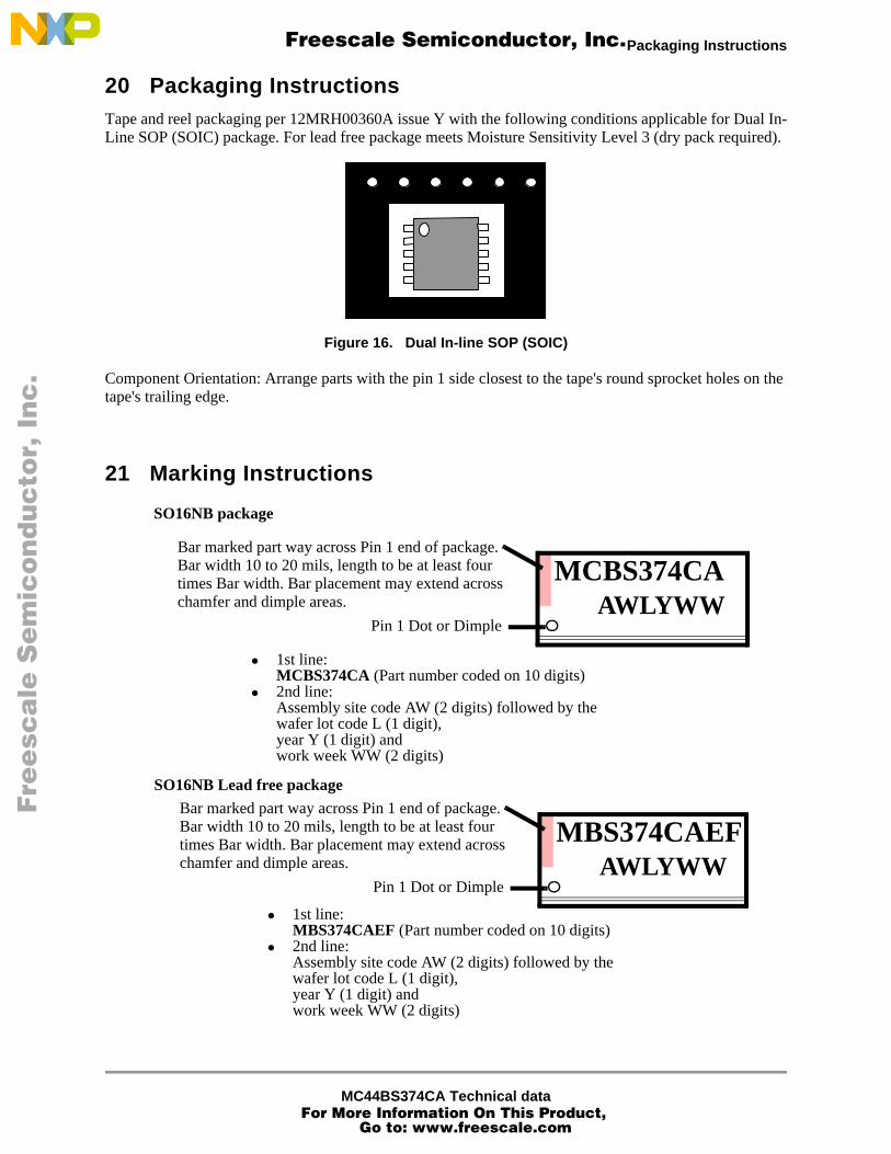
20 Packaging InstructionsTape and reel packaging per 12MRH00360A issue Y with the following conditions applicable for Dual In-Line SOP (SOIC) package. For lead free package meets Moisture Sensitivity Level 3 (dry pack required).
Figure 16. Dual In-line SOP (SOIC)
Component Orientation: Arrange parts with the pin 1 side closest to the tape's round sprocket holes on the tape's trailing edge.
21 Marking Instructions
Bar marked part way across Pin 1 end of package. Bar width 10 to 20 mils, length to be at least four times Bar width. Bar placement may extend across chamfer and dimple areas.
Pin 1 Dot or Dimple
• 1st line: MCBS374CA (Part number coded on 10 digits)
• 2nd line: Assembly site code AW (2 digits) followed by the wafer lot code L (1 digit), year Y (1 digit) and work week WW (2 digits)
MCBS374CAAWLYWW
Bar marked part way across Pin 1 end of package. Bar width 10 to 20 mils, length to be at least four times Bar width. Bar placement may extend across chamfer and dimple areas.
Pin 1 Dot or Dimple
• 1st line: MBS374CAEF (Part number coded on 10 digits)
• 2nd line: Assembly site code AW (2 digits) followed by the wafer lot code L (1 digit), year Y (1 digit) and work week WW (2 digits)
MBS374CAEFAWLYWW
SO16NB Lead free package
SO16NB package
Fre
esc
ale
Se
mic
on
du
cto
r, I
Freescale Semiconductor, Inc.
For More Information On This Product, Go to: www.freescale.com
nc
...

MC44BS374CA Technical data
Case Outline
22 Case Outline
Figure 17. SO16NB Package
DimMillimeters Inches
Min Max Min Max
A 1.35 1.75 0.054 0.068
A1 0.1 0.25 0.004 0.009
D 9.8 10 0.385 0.393
E 5.8 6.2 0.229 0.244
E1 3.8 4 0.150 0.157
b 0.35 0.49 0.014 0.019
c 0.19 0.25 0.008 0.009
e 1.27 BSC 0.050 BSC
L 0.4 1.25 0.016 0.049
h 0.25 0.5 0.010 0.019
Q 0o 7o 0o 7o
Note: 1. Dimensions and Tolerances per ASME Y14.5M, 1994.Note: 2. Controlling dimension: Millimeters.Note: 3. Dimension D and E1 do not include mold protrusion.Note: 4. Maximum mold protrusion 0.15 ( 0.006 ) per side.Note: 5. Dimension b does not include Dambar protrusion. Allowable Dambar protrusion shall be 0.127 ( 0.005 ) total in excess of the b dimension at maximum material condition.
Fre
esc
ale
Se
mic
on
du
cto
r, I
Freescale Semiconductor, Inc.
For More Information On This Product, Go to: www.freescale.com
nc
...

MC44BS374CA
Fre
esc
ale
Se
mic
on
du
cto
r, I
Freescale Semiconductor, Inc.
For More Information On This Product, Go to: www.freescale.com
nc
...
RXZB30
logo
RXZB30
disclaimer
RXZB30
hibbertleft
RXZB30
rohstext

MC44BS374CA Technical data
Case Outline
Fre
esc
ale
Se
mic
on
du
cto
r, I
Freescale Semiconductor, Inc.
For More Information On This Product, Go to: www.freescale.com
nc
...
Related Documents