Pin Connections MC33690 Order this document by MC33690/D SEMICONDUCTOR TECHNICAL MOTOROLA REV 4.8 © Motorola, Inc., 2002. This document contains information on a new product under development. Motorola reserves the right to change or discontinue this product without notice. Standalone Tag Reader Circuit STARC The Standalone Tag Reader Circuit (STARC) is an integrated circuit dedicated to the automotive immobilizer applications. It combines on the same chip all the circuitry to interface with a transponder : antenna drivers and demodulator. A low dropout voltage regulator and a physical interface fully compatible with the ISO 9141 norm are also available. The Standalone Tag Reader Circuit is fabricated with the SMARTMOS TM 3.5 technology. This process is a double layer metal, 1.4μm, 45V technology, combining CMOS and bipolar devices. • Contactless 125kHz tag reader module : - Self synchronous sample & hold demodulator - Amplitude or phase modulation detection - High sensitivity - Fast “read after write“ demodulator settling time - Low resistance and high current antenna drivers : 2Ω @ 150mA (typ.) - Bidirectionnal data transmission - Multi tag, multi scheme operation. • Low dropout voltage regulator : - Wide input supply voltage range : from 5.5V up to 40V - Output current capability up to 150mA DC with an external power transistor - 5V output voltage with a ± 5% accuracy - Low voltage reset function - Low current consumption in standby mode : 300μA (typ.). • ISO 9141 transmitter and receiver module : - Input voltage thresholds ratiometric to the supply voltage - Current limitation - Ouput slew rate control - No external protection device required. STANDALONE TAG READER CIRCUIT SOURCE TD1 VDD TD2 XTAL2 XTAL1 AM K Rx Tx 1 2 3 7 4 5 6 8 13 12 11 10 9 14 VSS VSUP GATE 15 16 17 20 19 18 MODE1 MODE2 RD LVR DOUT AGND CEXT ORDERING INFORMATION Device Operating Junction Temperature Range Package MC33690DW T J = -40°C to 125°C SOIC 20 DW SUFFIX Plastic Package CASE 751D SO - 20 Freescale Semiconductor, I Freescale Semiconductor, Inc. For More Information On This Product, Go to: www.freescale.com nc...

Welcome message from author
This document is posted to help you gain knowledge. Please leave a comment to let me know what you think about it! Share it to your friends and learn new things together.
Transcript
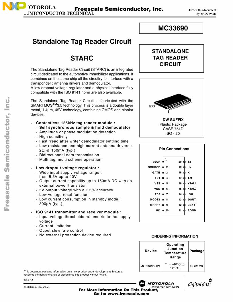
Pin Connections
MC33690
Order this documentby MC33690/DSEMICONDUCTOR TECHNICAL
MOTOROLA
REV 4.8
© Motorola, Inc., 2002.
This document contains information on a new product under development. Motorola reserves the right to change or discontinue this product without notice.
Standalone Tag Reader Circuit
STARCThe Standalone Tag Reader Circuit (STARC) is an integratedcircuit dedicated to the automotive immobilizer applications. Itcombines on the same chip all the circuitry to interface with atransponder : antenna drivers and demodulator.A low dropout voltage regulator and a physical interface fullycompatible with the ISO 9141 norm are also available.
The Standalone Tag Reader Circuit is fabricated with theSMARTMOSTM3.5 technology. This process is a double layermetal, 1.4µm, 45V technology, combining CMOS and bipolardevices.
• Contactless 125kHz tag reader module :- Self synchronous sample & hold demodulator- Amplitude or phase modulation detection- High sensitivity- Fast “read after write“ demodulator settling time- Low resistance and high current antenna drivers :
2Ω @ 150mA (typ.)- Bidirectionnal data transmission- Multi tag, multi scheme operation.
• Low dropout voltage regulator :- Wide input supply voltage range :
from 5.5V up to 40V- Output current capability up to 150mA DC with an
external power transistor- 5V output voltage with a ± 5% accuracy- Low voltage reset function- Low current consumption in standby mode :
300µA (typ.).
• ISO 9141 transmitter and receiver module :- Input voltage thresholds ratiometric to the supply
voltage - Current limitation- Ouput slew rate control- No external protection device required.
STANDALONETAG READER
CIRCUIT
SOURCE
TD1
VDD
TD2
XTAL2
XTAL1
AM
K
Rx
Tx1
2
3
7
4
5
6
8 13
12
1110
9
14
VSS
VSUP
GATE
15
16
17
20
19
18
MODE1
MODE2
RD
LVR
DOUT
AGND
CEXT
ORDERING INFORMATION
Device
OperatingJunction
TemperatureRange
Package
MC33690DWTJ = -40°C to
125°CSOIC 20
DW SUFFIXPlastic Package
CASE 751DSO - 20
Fre
esc
ale
Se
mic
on
du
cto
r, I
Freescale Semiconductor, Inc.
For More Information On This Product, Go to: www.freescale.com
nc
...
MC33690
MOTOROLA SEMICONDUCTORS PRODUCTS2
revision 4.8, 5 February 2002© Motorola, Inc., 2002.
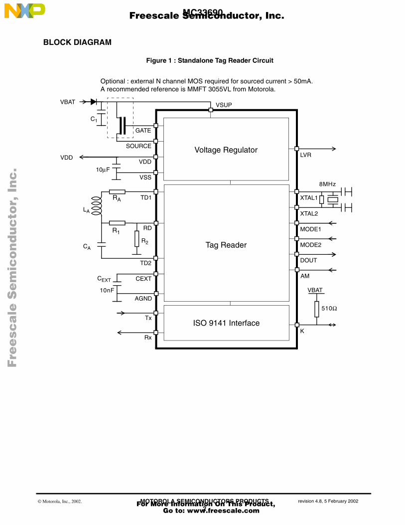
BLOCK DIAGRAM
Figure 1 : Standalone Tag Reader Circuit
VDD
VBAT VSUP
GATE
SOURCE
VDD
VSS
TD1
TD2
RD
XTAL1
XTAL2
MODE1
MODE2
DOUT
LVRVoltage Regulator
AMCEXT
AGND
Tag Reader
Tx
Rx
ISO 9141 Interface
VBAT
RA
CA
LA
R1
R2
CEXT
K
10µF
10nF
8MHz
510Ω
C1
Optional : external N channel MOS required for sourced current > 50mA.A recommended reference is MMFT 3055VL from Motorola.
Fre
esc
ale
Se
mic
on
du
cto
r, I
Freescale Semiconductor, Inc.
For More Information On This Product, Go to: www.freescale.com
nc
...
MC33690
MOTOROLA SEMICONDUCTORS PRODUCTS3
revision 4.8, 5 February 2002© Motorola, Inc., 2002.
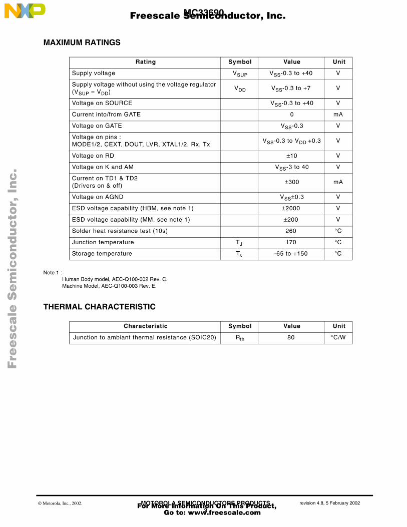
MAXIMUM RATINGS
Note 1 :Human Body model, AEC-Q100-002 Rev. C.Machine Model, AEC-Q100-003 Rev. E.
THERMAL CHARACTERISTIC
Rating Symbol Value Unit
Supply voltage VSUP VSS-0.3 to +40 V
Supply voltage without using the voltage regulator (VSUP = VDD)
VDD VSS-0.3 to +7 V
Voltage on SOURCE VSS-0.3 to +40 V
Current into/from GATE 0 mA
Voltage on GATE VSS-0.3 V
Voltage on pins : MODE1/2, CEXT, DOUT, LVR, XTAL1/2, Rx, Tx
VSS-0.3 to VDD +0.3 V
Voltage on RD ±10 V
Voltage on K and AM VSS-3 to 40 V
Current on TD1 & TD2 (Drivers on & off)
±300 mA
Voltage on AGND VSS±0.3 V
ESD voltage capability (HBM, see note 1) ±2000 V
ESD voltage capability (MM, see note 1) ±200 V
Solder heat resistance test (10s) 260 °C
Junction temperature TJ 170 °C
Storage temperature Ts -65 to +150 °C
Characteristic Symbol Value Unit
Junction to ambiant thermal resistance (SOIC20) Rth 80 °C/W
Fre
esc
ale
Se
mic
on
du
cto
r, I
Freescale Semiconductor, Inc.
For More Information On This Product, Go to: www.freescale.com
nc
...
MOTOROLA SEMICONDUCTORS PRODUCTS4
revision 4.8, 5 February 2002© Motorola, Inc., 2002.
MC33690
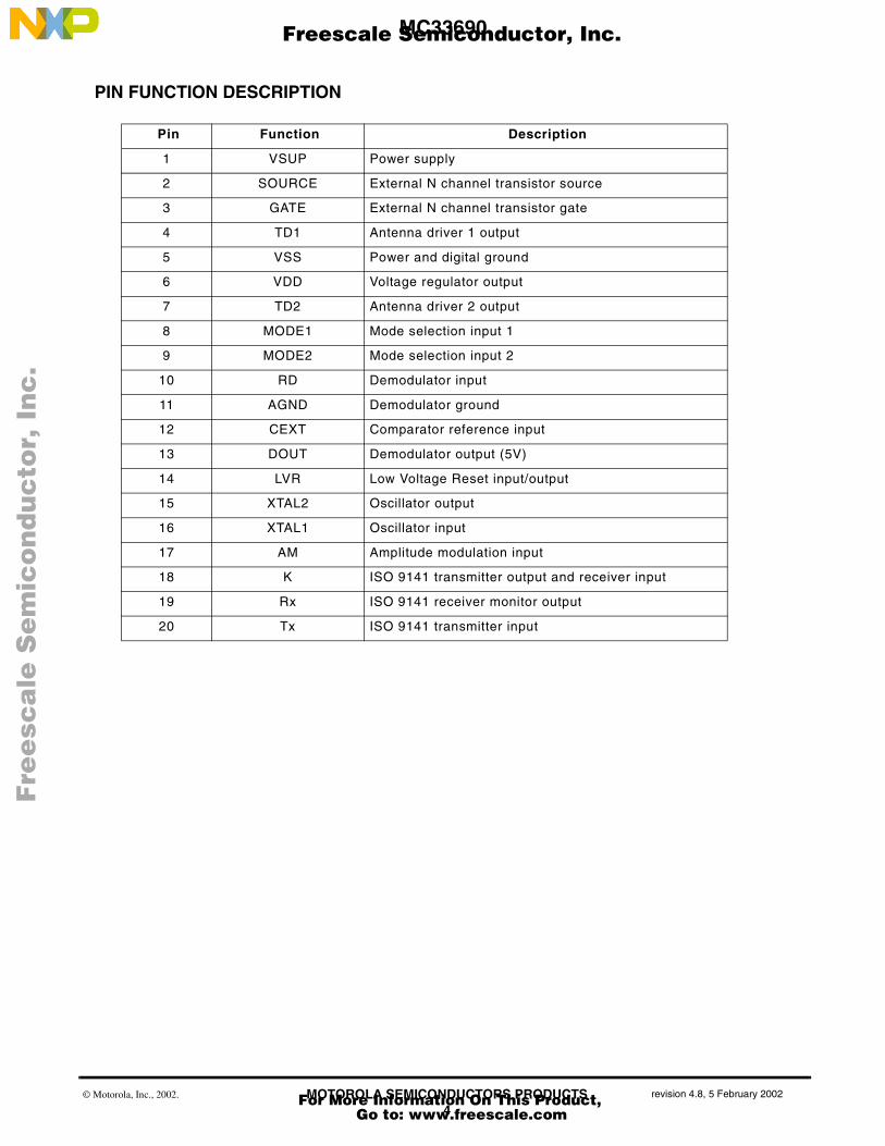
PIN FUNCTION DESCRIPTION
Pin Function Description
1 VSUP Power supply
2 SOURCE External N channel transistor source
3 GATE External N channel transistor gate
4 TD1 Antenna driver 1 output
5 VSS Power and digital ground
6 VDD Voltage regulator output
7 TD2 Antenna driver 2 output
8 MODE1 Mode selection input 1
9 MODE2 Mode selection input 2
10 RD Demodulator input
11 AGND Demodulator ground
12 CEXT Comparator reference input
13 DOUT Demodulator output (5V)
14 LVR Low Voltage Reset input/output
15 XTAL2 Oscillator output
16 XTAL1 Oscillator input
17 AM Amplitude modulation input
18 K ISO 9141 transmitter output and receiver input
19 Rx ISO 9141 receiver monitor output
20 Tx ISO 9141 transmitter input
Fre
esc
ale
Se
mic
on
du
cto
r, I
Freescale Semiconductor, Inc.
For More Information On This Product, Go to: www.freescale.com
nc
...
MOTOROLA SEMICONDUCTORS PRODUCTS5
revision 4.8, 5 February 2002© Motorola, Inc., 2002.
MC33690
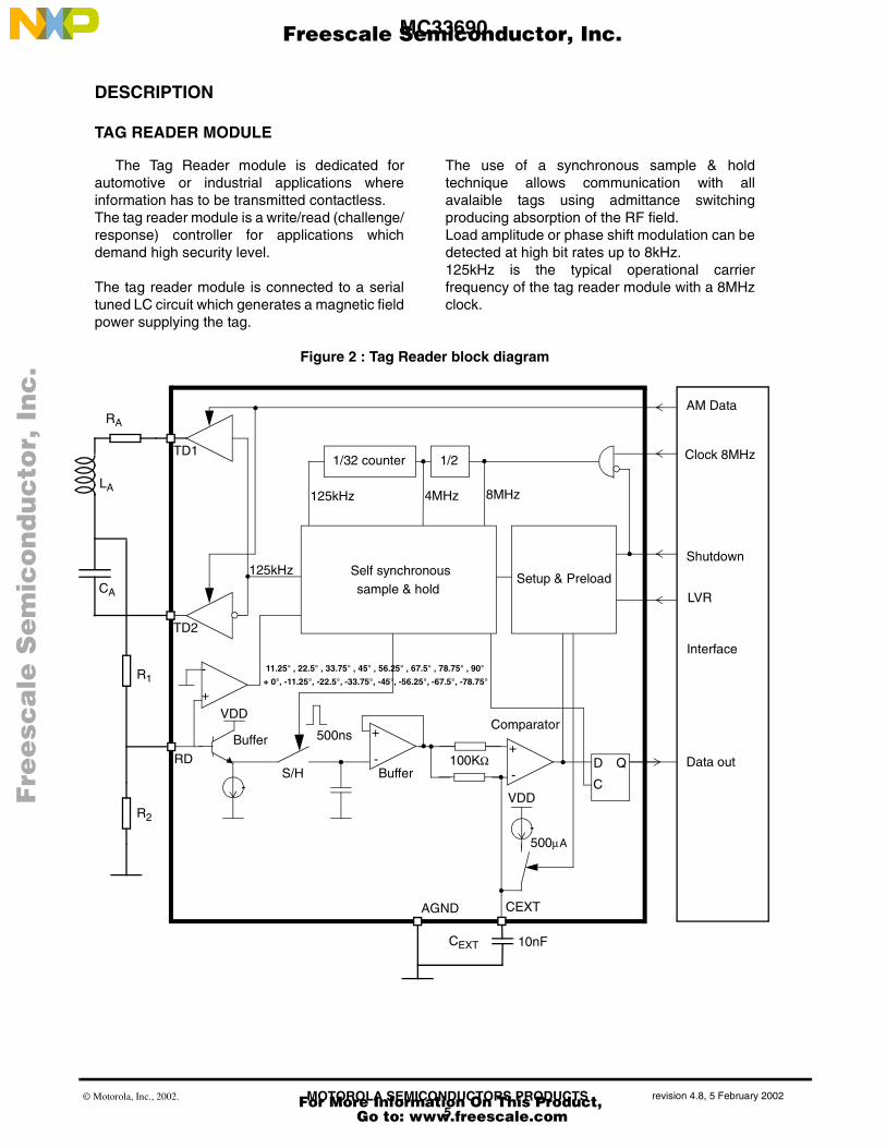
DESCRIPTION
TAG READER MODULE
The Tag Reader module is dedicated forautomotive or industrial applications whereinformation has to be transmitted contactless.The tag reader module is a write/read (challenge/response) controller for applications whichdemand high security level.
The tag reader module is connected to a serialtuned LC circuit which generates a magnetic fieldpower supplying the tag.
The use of a synchronous sample & holdtechnique allows communication with allavalaible tags using admittance switchingproducing absorption of the RF field.Load amplitude or phase shift modulation can bedetected at high bit rates up to 8kHz.125kHz is the typical operational carrierfrequency of the tag reader module with a 8MHzclock.
Figure 2 : Tag Reader block diagram
D
C
Q+
-
1/32 counter 1/2
RD
CEXTAGND
Buffer
VDD
500ns
S/H Buffer
Comparator
100KΩ
8MHz
Clock 8MHz
Data out
Interface
125kHz
TD2
11.25° , 22.5° , 33.75° , 45° , 56.25° , 67.5° , 78.75° , 90°
AM Data
+
-4MHz125kHz
LVR
Shutdown
TD1
10nF
+ 0°, -11.25°, -22.5°, -33.75°, -45°, -56.25°, -67.5°, -78.75°
CA
LA
R1
R2
CEXT
RA
VDD
+
-
Setup & Preload Self synchronous
sample & hold
500µA
Fre
esc
ale
Se
mic
on
du
cto
r, I
Freescale Semiconductor, Inc.
For More Information On This Product, Go to: www.freescale.com
nc
...
MOTOROLA SEMICONDUCTORS PRODUCTS6
revision 4.8, 5 February 2002© Motorola, Inc., 2002.
MC33690
Read function
When answering to the base station, atransponder generates an absorption modulationof the magnetic field. It results in an amplitude/phase modulation of the current across theantenna. This information is picked up at theantenna tap point between the coil and thecapacitor. An external resistive ladder downscales this voltage to a level compatible with thedemodulator input voltage range (see parameterVINRD page 16).The demodulator (see figure 2) consists of :
- an input stage (emitter follower),- a sample & hold circuit,- a voltage follower,- a low offset voltage comparator.
The sampling time is automatically set to takeinto account a phase shift due to the tolerancesof the antenna components (L and C) and of theoscillator. The allowed phase shift measured atthe input RD ranges from -45° to +45°. Assumingthat the phase reference is the falling edge of thedriving signal TD1, this leads to a sampling timephase ranging from -78.75° to 90° with discretesteps of 11.25°. After reset condition, thesampling time phase is +11.25°.
The antenna phase shift evaluation is onlydone :
- after each wake-up command (see pages10 to 12),
- or after reset (see page 7).This is necessary to obtain the best demodulatorperformances.In order to ensure a fast demodulator settlingtime after wake up, reset or a write sequence, theexternal capacitor CEXT is preloaded at itsworking voltage. This preset occurs 256µs after switching theantenna drivers on and its duration is 128µs.After wake up or reset, the preset has the sameduration but begins 518µs after clock settling.After power on reset, VSUP must meet theminimum specified value, enabling the nominaloperation of VDD, before the start of the preset.Otherwise the preset must be done by the userthrough a standby/wake-up sequence.
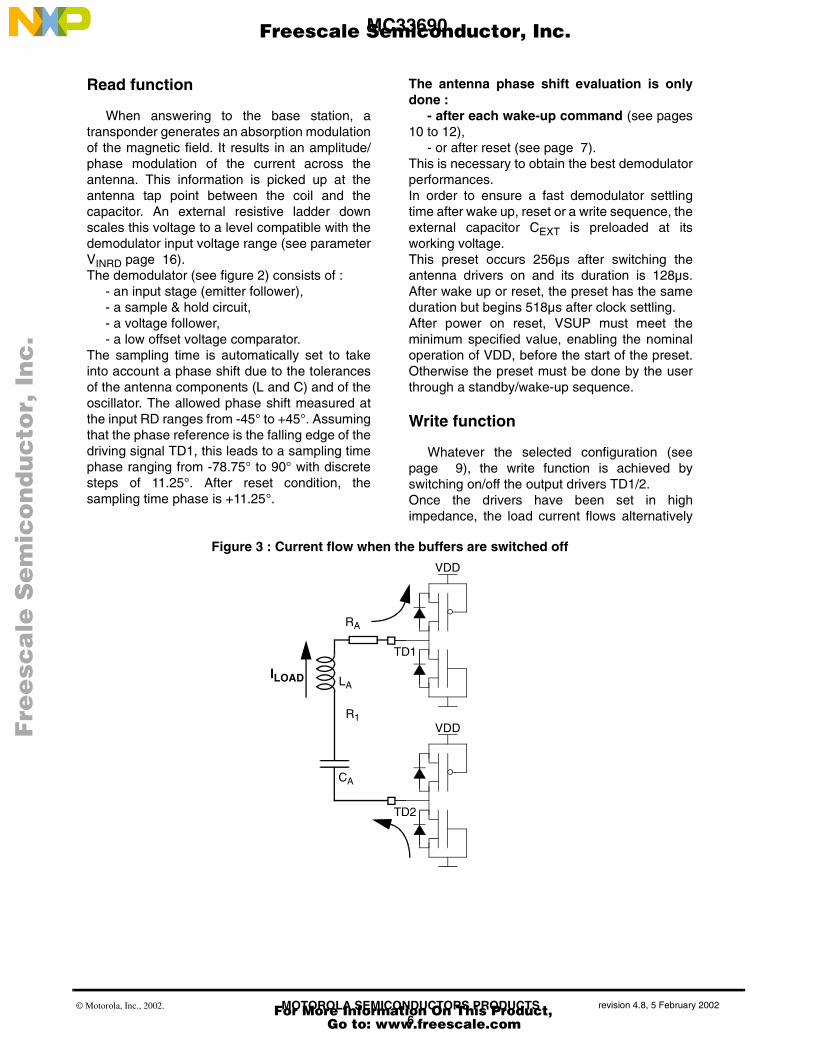
Write function
Whatever the selected configuration (seepage 9), the write function is achieved byswitching on/off the output drivers TD1/2.Once the drivers have been set in highimpedance, the load current flows alternatively
Figure 3 : Current flow when the buffers are switched off
CA
LA
R1
RA
TD1
VDD
TD2
VDD
ILOAD
Fre
esc
ale
Se
mic
on
du
cto
r, I
Freescale Semiconductor, Inc.
For More Information On This Product, Go to: www.freescale.com
nc
...
MOTOROLA SEMICONDUCTORS PRODUCTS7
revision 4.8, 5 February 2002© Motorola, Inc., 2002.
MC33690
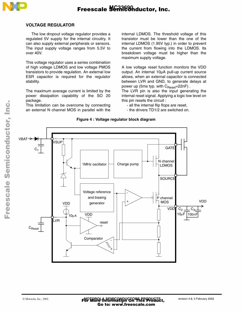
VOLTAGE REGULATOR
The low dropout voltage regulator provides aregulated 5V supply for the internal circuitry. Itcan also supply external peripherals or sensors.The input supply voltage ranges from 5.5V toover 40V.
This voltage regulator uses a series combinationof high voltage LDMOS and low voltage PMOStransistors to provide regulation. An external lowESR capacitor is required for the regulatorstability.
The maximum average current is limited by thepower dissipation capability of the SO 20package.This limitation can be overcome by connectingan external N channel MOS in parallel with the
internal LDMOS. The threshold voltage of thistransistor must be lower than the one of theinternal LDMOS (1.95V typ.) in order to preventthe current from flowing into the LDMOS. Itsbreakdown voltage must be higher than themaximum supply voltage.
A low voltage reset function monitors the VDDoutput. An internal 10µA pull-up current sourceallows, when an external capacitor is connectedbetween LVR and GND, to generate delays atpower up (5ms typ. with CReset=22nF) .The LVR pin is also the input generating theinternal reset signal. Applying a logic low level onthis pin resets the circuit :
- all the internal flip flops are reset,- the drivers TD1/2 are switched on.
Figure 4 : Voltage regulator block diagram
1MHz oscillator Charge pump
Voltage reference
and biasing
generator
+
-
VSUP
GATE
SOURCE
VDD
Comparator
N channelLDMOS
P channelMOS+
-
LVR
VBAT
C1
VDD
10µF 100nF
C3C2
10µA
VDD
CReset
VDD
reset
Fre
esc
ale
Se
mic
on
du
cto
r, I
Freescale Semiconductor, Inc.
For More Information On This Product, Go to: www.freescale.com
nc
...

MOTOROLA SEMICONDUCTORS PRODUCTS8
revision 4.8, 5 February 2002© Motorola, Inc., 2002.
MC33690
ISO 9141 PHYSICAL INTERFACE
This interface module is fully compatible withthe ISO 9141 norm describing the diagnosis line.It includes one transmitter (pin K) and 2 receivers(pins K and AM).
The input stages consist of high voltage CMOStriggers. The thresholds are ratiometric to VSUP.A ground referenced current source (2.5µA typ.)pulls down the input when unconnected.
When a negative voltage is applied on the K orAM lines, the input current is internally limited bya 2kΩ resistor (typ.) in series with a diode.
A current limitation allows the transmitter to drive
any capacitive load and protects against shortcircuit to the battery voltage. An overtemperatureprotection shuts the driver down when thejunction temperature exceeds 150°C (typ). Onceshut down by the overtemperature protection,the driver can be switched on again :
- if the junction temperature has decreasedbelow the threshold,
- and by applying an off/on command, comingeither from the demodulator in configurations Aand B or directly applied on the input Tx inconfiguration C (see pin K status in table 1 page9).
The electromagnetic emission is reduced thanksto the voltage slew rate control (5V/µs typ.).
Figure 5 : ISO 9141interface
Command
Rx
K
Tx
K line
VBAT
2kΩ
Over temperature
Current limitation
detector
VDD
VDD
Tag Reader module output
AMVSUP
From configuration controller
AM data
From configuration controller
L line
VSUP
VDD
GND2.5µA
GND2.5µA
2kΩ
GND
GND
Fre
esc
ale
Se
mic
on
du
cto
r, I
Freescale Semiconductor, Inc.
For More Information On This Product, Go to: www.freescale.com
nc
...
MOTOROLA SEMICONDUCTORS PRODUCTS9
revision 4.8, 5 February 2002© Motorola, Inc., 2002.
MC33690
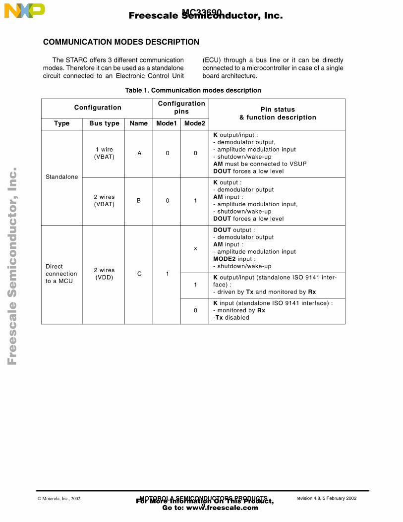
COMMUNICATION MODES DESCRIPTION
The STARC offers 3 different communicationmodes. Therefore it can be used as a standalonecircuit connected to an Electronic Control Unit
(ECU) through a bus line or it can be directlyconnected to a microcontroller in case of a singleboard architecture.
Table 1. Communication modes description
ConfigurationConfiguration
pins Pin status& function description
Type Bus type Name Mode1 Mode2
Standalone
1 wire (VBAT)
A 0 0
K output/input :- demodulator output,- amplitude modulation input- shutdown/wake-upAM must be connected to VSUPDOUT forces a low level
2 wires (VBAT)
B 0 1
K output :- demodulator outputAM input :- amplitude modulation input,- shutdown/wake-upDOUT forces a low level
Directconnectionto a MCU
2 wires (VDD)
C 1
x
DOUT output :- demodulator outputAM input :- amplitude modulation inputMODE2 input :- shutdown/wake-up
1K output/input (standalone ISO 9141 inter-face) :- driven by Tx and monitored by Rx
0K input (standalone ISO 9141 interface) :- monitored by Rx-Tx disabled
Fre
esc
ale
Se
mic
on
du
cto
r, I
Freescale Semiconductor, Inc.
For More Information On This Product, Go to: www.freescale.com
nc
...

MOTOROLA SEMICONDUCTORS PRODUCTS10
revision 4.8, 5 February 2002© Motorola, Inc., 2002.
MC33690
STANDALONE CONFIGURATION WITH ONE WIRE BUS
When a low level is applied on pins MODE1and MODE2, the circuit is in configuration A(standalone single wire bus configuration, seefigure 13 page 18).
After power on, the circuit is set into read mode.The demodulator output is directly routed to theISO 9141 interface output K.
The circuit can be set into write mode at anytimeby violation of all possible patterns on the singlewire bus during more than 1ms. Then the K lineachieves the amplitude modulation by switchingon/off both antenna drivers.After 1ms of inactivity at the end of the challengephase (bus in idle recessive one state), the circuitis set back into read mode.
The circuit can be put into standby mode byforcing the K line at zero during more than 2 msafter entering the write mode. Once the K line isreleased, the circuit sends an acknowledge pulsebefore entering into standby mode.In standby mode, the oscillator and most of theinternal biasing currents are switched off.Therefore, the functions (tag reader, ISO 9141driver) are inactive except the voltage regulatorand the ISO 9141 receiver on pin K. The driveroutput TD1 forces a low level and TD2 a highlevel. A rising edge on K wakes up the circuit.After completion of the wake-up sequence, thecircuit is automatically set in read mode.In configuration A, DOUT and Rx outputs alwaysforce a low level, Tx is disabled.
Figure 6 : Mode access description in one wire bus configuration
Figure 7 : Configuration A state diagram
K line T0 ≤ t < T0’+T1’ 1 0 0 01 1
read mode write mode
K line t ≥T0
read modewrite mode
K line t ≥ T1
standby modewrite mode
Read to write mode :
Write to read mode :
Write to standby mode :
Standby mode to read mode :
standby mode read modewake-up sequence
K line
acknowledge
T2 T2
read
writeTD1/2
writeTD1/2 off
standby
T0 ≤ K line low
K line high < T0’
T1 ≤ K line low
T0 ≤ K line high
wake up
K line low
reset
K
switching
Fre
esc
ale
Se
mic
on
du
cto
r, I
Freescale Semiconductor, Inc.
For More Information On This Product, Go to: www.freescale.com
nc
...
MOTOROLA SEMICONDUCTORS PRODUCTS11
revision 4.8, 5 February 2002© Motorola, Inc., 2002.
MC33690
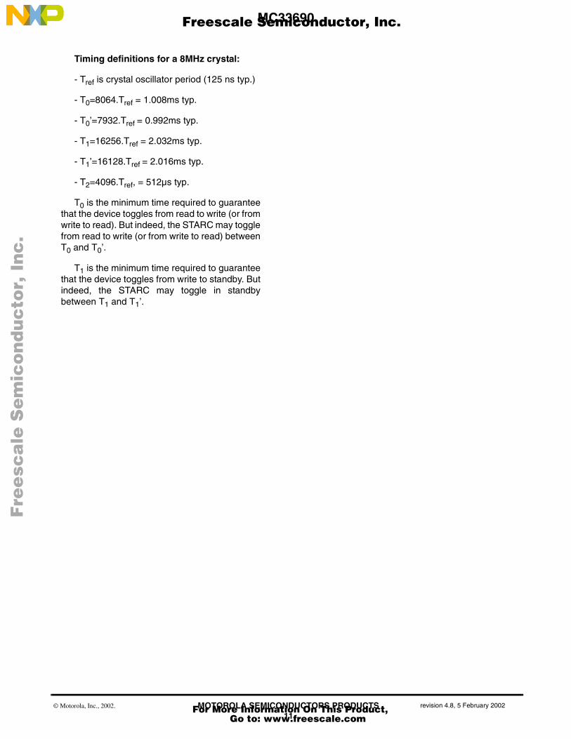
Timing definitions for a 8MHz crystal:
- Tref is crystal oscillator period (125 ns typ.)
- T0=8064.Tref = 1.008ms typ.
- T0’=7932.Tref = 0.992ms typ.
- T1=16256.Tref = 2.032ms typ.
- T1’=16128.Tref = 2.016ms typ.
- T2=4096.Tref, = 512µs typ.
T0 is the minimum time required to guaranteethat the device toggles from read to write (or fromwrite to read). But indeed, the STARC may togglefrom read to write (or from write to read) betweenT0 and T0’.
T1 is the minimum time required to guaranteethat the device toggles from write to standby. Butindeed, the STARC may toggle in standbybetween T1 and T1’.
Fre
esc
ale
Se
mic
on
du
cto
r, I
Freescale Semiconductor, Inc.
For More Information On This Product, Go to: www.freescale.com
nc
...
MOTOROLA SEMICONDUCTORS PRODUCTS12
revision 4.8, 5 February 2002© Motorola, Inc., 2002.
MC33690
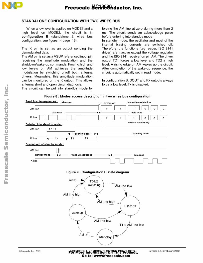
STANDALONE CONFIGURATION WITH TWO WIRES BUS
When a low level is applied on MODE1 and ahigh level on MODE2, the circuit is inconfiguration B (standalone 2 wires busconfiguration, see figure 14 page 19).
The K pin is set as an output sending thedemodulated data. The AM pin is set as a VSUP referenced input pinreceiving the amplitude modulation and theshutdown/wake-up commands. Forcing high andlow levels on AM achieves the amplitudemodulation by switching on/off both antennadrivers. Meanwhile, this amplitude modulationcan be monitored on the K output. This allowsantenna short and open circuit diagnosis.The circuit can be put into standby mode by
forcing the AM line at zero during more than 2ms. The circuit sends an acknowledge pulsebefore entering into standby modeIn standby mode, the oscillator and most of theinternal biasing currents are switched off.Therefore, the functions (tag reader, ISO 9141driver) are inactive except the voltage regulatorand the ISO 9141 receiver on pin AM. The driveroutput TD1 forces a low level and TD2 a highlevel. A rising edge on AM wakes up the circuit.After completion of the wake-up sequence, thecircuit is automatically set in read mode.
In configuration B, DOUT and Rx outputs alwaysforce a low level, Tx is disabled.
Figure 8 : Modes access description in two wires bus configuration
Figure 9 : Configuration B state diagram
AM line 1 0 0 01 1
data read
drivers off
AM line t ≥ T1
standby mode
Read & write sequences :
1 0 0 01 1K line
Entering into standby mode :
K line
data write modulation
data write
AM line monitoring
drivers on
wake-up sequence data read
T2 T2T1
Coming out of standby mode :
AM line
K line
standby mode
acknowledge
TD1/2 off
TD1/2
standby
AM line high
wake up
AM line low
T1 ≤ AM line low
reset
AM line high
AM line low
AM
switching
Fre
esc
ale
Se
mic
on
du
cto
r, I
Freescale Semiconductor, Inc.
For More Information On This Product, Go to: www.freescale.com
nc
...
MOTOROLA SEMICONDUCTORS PRODUCTS13
revision 4.8, 5 February 2002© Motorola, Inc., 2002.
MC33690
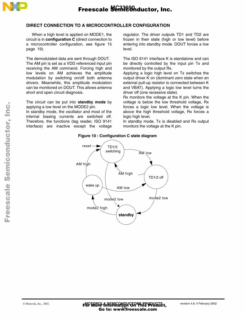
DIRECT CONNECTION TO A MICROCONTROLLER CONFIGURATION
When a high level is applied on MODE1, thecircuit is in configuration C (direct connection toa microcontroller configuration, see figure 15page 19).
The demodulated data are sent through DOUT. The AM pin is set as a VDD referenced input pinreceiving the AM command. Forcing high andlow levels on AM achieves the amplitudemodulation by switching on/off both antennadrivers. Meanwhile, this amplitude modulationcan be monitored on DOUT. This allows antennashort and open circuit diagnosis.
The circuit can be put into standby mode byapplying a low level on the MODE2 pin. In standby mode, the oscillator and most of theinternal biasing currents are switched off.Therefore, the functions (tag reader, ISO 9141interface) are inactive except the voltage
regulator. The driver outputs TD1 and TD2 arefrozen in their state (high or low level) beforeentering into standby mode. DOUT forces a lowlevel.
The ISO 9141 interface K is standalone and canbe directly controlled by the input pin Tx andmonitored by the output Rx.Applying a logic high level on Tx switches theoutput driver K on (dominant zero state when anexternal pull-up resistor is connected between Kand VBAT). Applying a logic low level turns thedriver off (one recessive state).Rx monitors the voltage at the K pin. When thevoltage is below the low threshold voltage, Rxforces a logic low level. When the voltage isabove the high threshold voltage, Rx forces alogic high level.In standby mode, Tx is disabled and Rx outputmonitors the voltage at the K pin.
Figure 10 : Configuration C state diagram
TD1/2 off
standby
wake up
mode2 low
mode2 high
mode2 low
TD1/2
AM high
AM high
AM low
reset
AM low
switching
Fre
esc
ale
Se
mic
on
du
cto
r, I
Freescale Semiconductor, Inc.
For More Information On This Product, Go to: www.freescale.com
nc
...

MC33690
MOTOROLA SEMICONDUCTORS PRODUCTS14
revision 4.8, 5 February 2002© Motorola, Inc., 2002.
ELECTRICAL CHARACTERISTICS
Typical values reflect average measurements at VSUP=12V and TJ=25°C.
SUPPLY CURRENT
6V ≤ VSUP ≤ 16V, VSS = 0V, TJ = –40°C to +125°C, unless otherwise noted
VOLTAGE REGULATOR
6V ≤ VSUP ≤ 16V, VSS = 0V, TJ = –40°C to +125°C, unless otherwise noted
Parameter SymbolTest Conditions
& Comments Min Typ Max Unit Type
Pin VSUP
9.1 Standby mode current ISUP1 - 300 500 µA
9.2 Operating mode current ISUP2 See note 1
1. Circuit in configuration C, no current sunk from VDD, drivers TD1/2 switched off, Tx forced to low.- 1.5 2.5 mA
Parameter SymbolTest Conditions
& CommentsMin Typ Max Unit Type
Pins VSUP & VDD
1.1 Output Voltage (5.5V ≤ VSUP ≤ 40V) VVDD1 Without external MOS transistorIOUT ≤ 50mA
4.75 5.0 5.25 V
1.3 Total Output Current IVDD1 - - 50 mA
1.5 Load Regulation VLoadReg1Without external MOS transistor
1 to 50mA IOUT change - 20 60 mV
1.9 Output Voltage (5.5V ≤ VSUP ≤ 40V) VVDD2 With external MOS transistor, see notes 1 and 2
IOUT ≤ 150mA
1. The stability is ensured with a decoupling capacitor between VDD and VSS : COUT ≥ 10µF with ESR ≤ 3Ω.2. The current capability can be increased up to 150mA by using an external N channel MOS transistor (see figure 1 page 2). The main
characteristics for choosing this component are : VT < 1.8V and BVDSS > 40V.
4.7 5.0 5.3 V
1.11 Total Output Current IVDD2 - - 150 mA
1.6 Load Regulation VLoadReg2With external MOS transistor
1 to 150mA IOUT change- 65 150 mV
1.4 Line Regulation (6V ≤ VSUP ≤ 16V) VLineReg IOUT = 1mA -15 -1 - mV
Fre
esc
ale
Se
mic
on
du
cto
r, I
Freescale Semiconductor, Inc.
For More Information On This Product, Go to: www.freescale.com
nc
...
MC33690
MOTOROLA SEMICONDUCTORS PRODUCTS15
revision 4.8, 5 February 2002© Motorola, Inc., 2002.
LOW VOLTAGE RESET
6V ≤ VSUP ≤ 16V, VSS = 0V, TJ = –40°C to +125°C, unless otherwise noted
Figure 11 : Low voltage reset waveform
OSCILLATOR
6V ≤ VSUP ≤ 16V, VSS = 0V, TJ = –40°C to +125°C, unless otherwise noted
Parameter SymbolTest Conditions
& CommentsMin Typ Max Unit Type
Pin LVR
1.6 Low Voltage Reset Low Threshold VLVRON See note 1 and figure 11
1. As the voltage regulator and the low voltage reset are using the same internal voltage reference, it is ensured that the low voltage resetwill only occur when the voltage regulator is out of regulation.
4.1 4.35 4.6 V
1.7 Low Voltage Reset Hysteresis VLVRH 50 100 150 mV
1.12 Pull-up Current ILVRUP VLVR = 2.5V 5 10 15 µA
1.13 Output Resistance in reset condition RLVR VLVR = 2.5V 200 370 500 Ω
1.14 Input Low Voltage VILLVR 0 -0.3 xVDD
V
1.15 Input High Voltage VIHLVR0.7 xVDD
- VDD V
Characteristic SymbolTest Condition& Comments
Min Typ Max Unit Type
Pins XTAL1, XTAL2
8.0 Input Capacitance CXTAL1 VXTAL1 = 2.5V - 5 - pF
8.1 Voltage gain VXTAL2 / VXTAL1 AOSC VXTAL1 = 2.5V - 25 - -
8.3 Clock input level VXTAL1 See note 1
1. This level ensures the circuit operation with a 8MHz clock. It is applied through a capacitive coupling. A 1MΩ resistor connected betweenXTAL1 and XTAL2 biases the oscillator input.
1.5 - VDD Vpp
VDD
LVR
VLVRON
VLVRON + VLVRH
Fre
esc
ale
Se
mic
on
du
cto
r, I
Freescale Semiconductor, Inc.
For More Information On This Product, Go to: www.freescale.com
nc
...
MC33690
MOTOROLA SEMICONDUCTORS PRODUCTS16
revision 4.8, 5 February 2002© Motorola, Inc., 2002.
TAG READER
6V ≤ VSUP ≤ 16V, VSS = 0V, TJ = –40°C to +125°C, unless otherwise noted
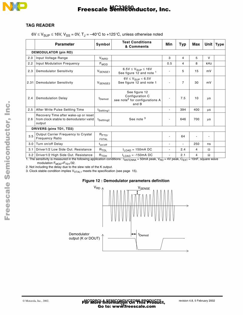
Figure 12 : Demodulator parameters definition
Parameter SymbolTest Conditions
& CommentsMin Typ Max Unit Type
DEMODULATOR (pin RD)
2.0 Input Voltage Range VINRD 3 4 5 V
2.2 Input Modulation Frequency FMOD 0.5 4 8 kHz
2.3 Demodulator Sensitivity VSENSE16.5V ≤ VSUP ≤ 16V
See figure 12 and note 1
1. The sensitivity is measured in the following application conditions : IANTENNA = 50mA peak, VRD = 4V peak, CEXT = 10nF, square wavemodulation FMOD=FTD1/32.
- 5 15 mV
2.31 Demodulator Sensitivity VSENSE2
6V ≤ VSUP < 6.5VSee figure 12 and note 1 - 7 30 mV
2.4 Demodulation Delay tDemod
See figure 12Configuration C
see note2 for configurations A and B
2. Not including the delay due to the slew rate of the K output.
- 7.5 10 µs
2.5 After Write Pulse Settling Time tSettling1 - 394 400 µs
2.6Recovery Time after wake-up or reset from clock stable to demodulator valid output
tSettling2 See note 3
3. Clock stable condition implies VXTAL1 meets the specification (see page 15).
- 646 700 µs
DRIVERS (pins TD1, TD2)
3.5Output Carrier Frequency to Crystal Frequency Ratio
RFTD/
FXTAL- 64 - -
3.0 Turn on/off Delay ton/off - - 250 ns
3.1 Driver1/2 Low Side Out. Resistance RTDL ILOAD = 150mA DC - 2.4 4 Ω
3.2 Driver1/2 High Side Out. Resistance RTDH ILOAD = -150mA DC - 2.1 4 Ω
Demodulator
VRD VSENSE
tDemodoutput (K or DOUT)
Fre
esc
ale
Se
mic
on
du
cto
r, I
Freescale Semiconductor, Inc.
For More Information On This Product, Go to: www.freescale.com
nc
...
MC33690
MOTOROLA SEMICONDUCTORS PRODUCTS17
revision 4.8, 5 February 2002© Motorola, Inc., 2002.
ISO 9141 INTERFACE
6V ≤ VSUP ≤ 16V, VSS = 0V, TJ = –40°C to +125°C, unless otherwise noted
DIGITAL I/O
6V ≤ VSUP ≤ 16V, VSS = 0V, TJ = –40°C to +125°C, unless otherwise noted
Parameter SymbolTest Conditions
& CommentsMin Typ Max Unit Type
Receiver (pins K & AM)
4.0 Input Low Voltage VIL -3 -0.3 xVSUP
V
4.1 Input High Voltage VIH0.65 xVSUP
- 40 V
4.2 Input Hysteresis Voltage VHY1 0.4 0.65 1.3 V
4.3 Biasing Current IB 0V ≤ VIN ≤ 16V 1 3 5 µA
4.31 Input Current IBM -3 ≤ VIN < 0 -2 -1 - mA
4.4 K to Rx delay tdkrx 2 10 µs
Driver (pin K)
5.0 Output Falling Edge Slew Rate SRF
RPull-up = 510Ω,see note 1
1. Calculated from 20% to 80% of the output swing.
3.5 5 6.5 V/µs
5.1 Output Rising Edge Slew Rate SRR 3.5 5 6.5 V/µs
5.2 Rise Fall Slew Rates SymmetrySRSYME-
TRY-1 0 1 V/µs
5.3 Output Low Voltage VOLK ILOAD = 25mA - 1.1 1.4 V
5.4Input Current(driver switched on or off)
IIK -3V ≤ VIN ≤ 0V -2 - 0 mA
5.5 Current Limitation Threshold IL 0V ≤ VIN ≤ 40V 35 50 65 mA
5.6 Thermal Shutdown Threshold THSDWN 130 150 170 °C
Characteristic SymbolTest Condition& Comments
Min Typ Max Unit Type
INPUT (pins MODE1, MODE2, AM, TX)
6.0 Input Low Voltage VILD 0 -0.3 xVDD
V
6.1 Input High Voltage VIHD0.7 xVDD
- VDD V
6.2 Input Hysteresis VoltageVHD .24 .7 1 V
OUTPUT (pins DOUT,RX)
7.0 Output Low Voltage VOL ILOAD = 500uA 0 0.50.2 xVDD
V
7.1 Output High Voltage VOH ILOAD = -500uA0.8 xVDD
4.6 VDD V
7.2 Fall/Rise Time tF/R CLOAD=10pF, see note 1
1. Calculated from 10% to 90% of the output swing.- - 150 ns
Fre
esc
ale
Se
mic
on
du
cto
r, I
Freescale Semiconductor, Inc.
For More Information On This Product, Go to: www.freescale.com
nc
...
MC33690
MOTOROLA SEMICONDUCTORS PRODUCTS18
revision 4.8, 5 February 2002© Motorola, Inc., 2002.
APPLICATION SCHEMES
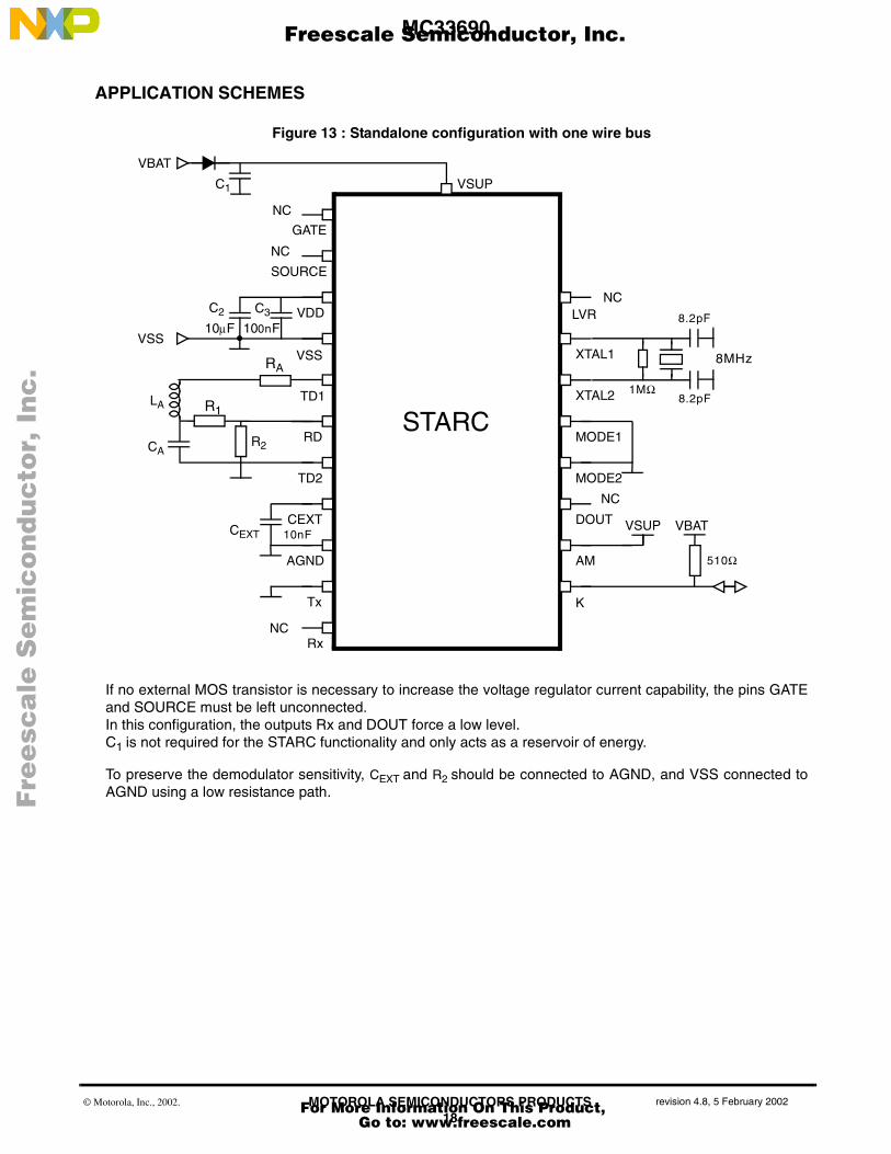
Figure 13 : Standalone configuration with one wire bus
VBAT
VSUP
GATE
SOURCE
TD1
TD2
RD
XTAL1
XTAL2
MODE1
MODE2
DOUT
LVR
AM
CEXT
AGND
STARC
Tx
Rx
CEXT
10µF
10nF
8MHz
VDD
VSS
100nF
NC
NC
VSUP
NC
510Ω
VBAT
K
VSS
C1
C3C2
RA
CA
LA R1
R2
If no external MOS transistor is necessary to increase the voltage regulator current capability, the pins GATEand SOURCE must be left unconnected.In this configuration, the outputs Rx and DOUT force a low level.C1 is not required for the STARC functionality and only acts as a reservoir of energy.
To preserve the demodulator sensitivity, CEXT and R2 should be connected to AGND, and VSS connected toAGND using a low resistance path.
NC
NC
1MΩ8.2pF
8.2pF
Fre
esc
ale
Se
mic
on
du
cto
r, I
Freescale Semiconductor, Inc.
For More Information On This Product, Go to: www.freescale.com
nc
...
MC33690
MOTOROLA SEMICONDUCTORS PRODUCTS19
revision 4.8, 5 February 2002© Motorola, Inc., 2002.
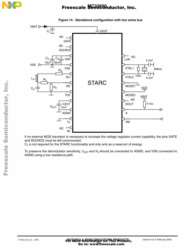
Figure 14 : Standalone configuration with two wires bus
VBAT
VSUP
GATE
SOURCE
TD1
TD2
RD
XTAL1
XTAL2
MODE1
MODE2
DOUT
LVR
AM
CEXT
AGND
STARC
Tx
Rx
RA
CA
LA R1
R2
CEXT
10µF
10nF
VDD
VSS
100nF
NC
NC
NC510Ω
VDD
K
VSS
C1
C3C2
VBAT
NC
NC
If no external MOS transistor is necessary to increase the voltage regulator current capability, the pins GATEand SOURCE must be left unconnected.C1 is not required for the STARC functionality and only acts as a reservoir of energy.
To preserve the demodulator sensitivity, CEXT and R2 should be connected to AGND, and VSS connected toAGND using a low resistance path.
8MHz
1MΩ8.2pF
8.2pF
Fre
esc
ale
Se
mic
on
du
cto
r, I
Freescale Semiconductor, Inc.
For More Information On This Product, Go to: www.freescale.com
nc
...
MC33690
MOTOROLA SEMICONDUCTORS PRODUCTS20
revision 4.8, 5 February 2002© Motorola, Inc., 2002.
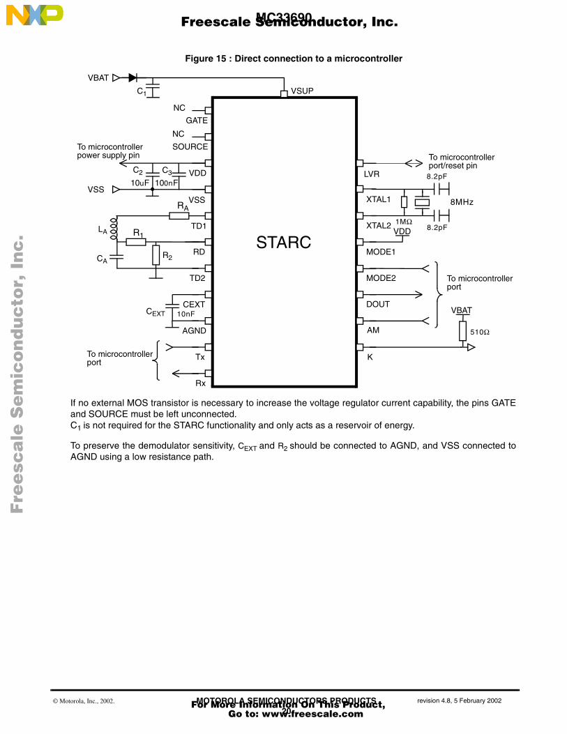
Figure 15 : Direct connection to a microcontroller
VBAT
VSUP
GATE
SOURCE
TD1
TD2
RD
XTAL1
XTAL2
MODE1
MODE2
DOUT
LVR
AM
CEXT
AGND
STARC
Tx
Rx
CEXT
10uF
10nF
VDD
VSS
100nF
NC
NC
510Ω
VBAT
K
VSS
C1
C3C2
VDD
To microcontrollerport
To microcontrollerport
To microcontroller To microcontrollerpower supply pin
RA
CA
LA R1
R2
If no external MOS transistor is necessary to increase the voltage regulator current capability, the pins GATEand SOURCE must be left unconnected.C1 is not required for the STARC functionality and only acts as a reservoir of energy.
To preserve the demodulator sensitivity, CEXT and R2 should be connected to AGND, and VSS connected toAGND using a low resistance path.
8MHz
1MΩ8.2pF
8.2pFport/reset pin
Fre
esc
ale
Se
mic
on
du
cto
r, I
Freescale Semiconductor, Inc.
For More Information On This Product, Go to: www.freescale.com
nc
...

MC33690
MOTOROLA SEMICONDUCTORS PRODUCTS21
revision 4.8, 5 February 2002© Motorola, Inc., 2002.
Notes
Fre
esc
ale
Se
mic
on
du
cto
r, I
Freescale Semiconductor, Inc.
For More Information On This Product, Go to: www.freescale.com
nc
...

MC33690
MOTOROLA SEMICONDUCTORS PRODUCTS22
revision 4.8, 5 February 2002© Motorola, Inc., 2002.
Notes
Fre
esc
ale
Se
mic
on
du
cto
r, I
Freescale Semiconductor, Inc.
For More Information On This Product, Go to: www.freescale.com
nc
...
MC33690
MOTOROLA SEMICONDUCTORS PRODUCTS23
revision 4.8, 5 February 2002© Motorola, Inc., 2002.
Notes
Fre
esc
ale
Se
mic
on
du
cto
r, I
Freescale Semiconductor, Inc.
For More Information On This Product, Go to: www.freescale.com
nc
...
MC33690
Motorola reserves the right to make changes without further notice to any products herein. Motorola makes no warranty, representation or guarantee regarding
the suitability of its products for any particular purpose, nor does Motorola assume any liability arising out of the application or use of any product or circuit, and
specifically disclaims any and all liability, including without limitation consequential or incidental damages. “Typical” parameters which may be provided in Motorola
data sheets and/or specifications can and do vary in different applications and actual performance may vary over time. All operating parameters, including
“Typicals” must be validated for each customer application by customer’s technical experts. Motorola does not convey any license under its patent rights nor the
rights of others. Motorola products are not designed, intended, or authorized for use as components in systems intended for surgical implant into the body, or
other applications intended to support or sustain life, or for any other application in which the failure of the Motorola product could create a situation where personal
injury or death may occur. Should Buyer purchase or use Motorola products for any such unintended or unauthorized application, Buyer shall indemnify and hold
Motorola and its officers, employees, subsidiaries, affiliates, and distributors harmless against all claims, costs, damages, and expenses, and reasonable attorney
fees arising out of, directly or indirectly, any claim of personal injury or death associated with such unintended or unauthorized use, even if such claim alleges that
Motorola was negligent regarding the design or manufacture of the part. Motorola and the Stylized M Logo are registered in the U.S. Patent and Trademark Office.
Motorola, Inc. is an Equal Opportunity/Affirmative Action Employer. All other product or service names are the property of their respective owners.
© Motorola, Inc. 2002
HOW TO REACH US:USA/EUROPE/LOCATIONS NOT LISTED: Motorola Literature Distribution: P.O. Box 5405, Denver, Colorado 80217. 1-303-675-2140 or 1-800-441-2447
JAPAN: Motorola Japan Ltd.; SPS, Technical Information Center, 3-20-1 Minami-Azabu. Minato-ku, Tokyo 106-8573 Japan. 81-3-3440-3569
ASIA/PACIFIC: Motorola Semiconductors H.K. Ltd.; Silicon Harbour Centre, 2 Dai King Street, Tai Po Industrial Estate, Tao Po, N.T.,Hong Kong. 852-26668334
TECHNICAL INFORMATION CENTER: 1-800-521-6274
HOME PAGE: http://motorola.com/semiconductors/
MC33690/D
Fre
esc
ale
Se
mic
on
du
cto
r, I
Freescale Semiconductor, Inc.
For More Information On This Product, Go to: www.freescale.com
nc
...
Related Documents