Document Number: MC06XS4200 Rev. 4.0, 4/2014 Freescale Semiconductor Advance Information © Freescale Semiconductor, Inc., 2012 - 2014. All rights reserved. *This document contains certain information on a product under development. Freescale reserves the right to change or discontinue this product without notice Dual 24 V, 6.0 mOhm High-side Switch The 06XS4200 device is part of a 24 V dual high-side switch product family with integrated control and a high number of protective and diagnostic functions. It has been designed for truck, bus, and industrial applications. The low R DS(on) channels (<6.0 mOhm) can control different load types; bulbs, solenoids, or DC motors. Control, device configuration, and diagnostics are performed through a 16-bit serial peripheral interface (SPI), allowing easy integration into existing applications. Both channels can be controlled individually by external/internal clock- signals or by direct inputs. Using the internal clock allows fully autonomous device operation. Programmable output voltage slew rates (individually programmable) help improve EMC performance. To avoid shutting off the device during inrush current, while still being able to closely track the load current, a dynamic overcurrent threshold profile is featured. Switching current of each channel can be sensed with a programmable sensing ratio. Whenever communication with the external microcontroller is lost, the device enters a fail-safe operation mode, but remains operational, controllable, and protected. This device is powered using SMARTMOS technology. Features • Two fully-protected 6.0 mOhm (@ 25 °C) high-side switches • Up to 9.0 A steady-state current per channel • Separate bulb and DC motor latched overcurrent handling • Parallel output operating mode with improved switching synchronization • Individually programmable internal/external PWM clock signals (switching frequency, duty cycle, slew rate, switch-on time-shift) • Overcurrent, short-circuit, and overtemperature protection with programmable auto-retry functions • Accurate temperature and current sensing (high/low sensing ratios/offset compensation) • OpenLoad detection (channel in OFF and ON state), also for LED applications (7.0 mA typ.) • Normal operating range: 8.0 - 36 V, extended range: 6.0 - 58 V, 3.3 V and 5.0 V compatible 16-bit SPI port for device control, configuration, and diagnostics at rates up to 8.0 MHz Figure 1. Simplified Application Diagram FK SUFFIX (PB-FREE) 98ASA00428D 23 PIN PQFN (12 X12 mm) 06XS4200 High-side Switch MCU V DD CLOCK FSB SCLK CSB SO RSTB SI IN0 IN1 CSNS GND VDD VPWR HS0 HS1 LOAD I/O SCLK CSB SI I/O SO I/O I/O A/D GND LOAD M CONF0 CONF1 FSOB I/O A/D SYNC I/O 06XS4200 V DD V PWR

Welcome message from author
This document is posted to help you gain knowledge. Please leave a comment to let me know what you think about it! Share it to your friends and learn new things together.
Transcript

Document Number: MC06XS4200Rev. 4.0, 4/2014
Freescale Semiconductor Advance Information
*This document contains certain information on a product under development.
Dual 24 V, 6.0 mOhm High-side SwitchThe 06XS4200 device is part of a 24 V dual high-side switch product family with integrated control and a high number of protective and diagnostic functions. It has been designed for truck, bus, and industrial applications. The low RDS(on) channels (<6.0 mOhm) can control different load types; bulbs, solenoids, or DC motors. Control, device configuration, and diagnostics are performed through a 16-bit serial peripheral interface (SPI), allowing easy integration into existing applications.Both channels can be controlled individually by external/internal clock-signals or by direct inputs. Using the internal clock allows fully autonomous device operation. Programmable output voltage slew rates (individually programmable) help improve EMC performance. To avoid shutting off the device during inrush current, while still being able to closely track the load current, a dynamic overcurrent threshold profile is featured. Switching current of each channel can be sensed with a programmable sensing ratio. Whenever communication with the external microcontroller is lost, the device enters a fail-safe operation mode, but remains operational, controllable, and protected. This device is powered using SMARTMOS technology.Features
• Two fully-protected 6.0 mOhm (@ 25 °C) high-side switches• Up to 9.0 A steady-state current per channel• Separate bulb and DC motor latched overcurrent handling• Parallel output operating mode with improved switching
synchronization• Individually programmable internal/external PWM clock signals
(switching frequency, duty cycle, slew rate, switch-on time-shift)• Overcurrent, short-circuit, and overtemperature protection with
programmable auto-retry functions• Accurate temperature and current sensing (high/low sensing
ratios/offset compensation)• OpenLoad detection (channel in OFF and ON state), also for LED
applications (7.0 mA typ.)• Normal operating range: 8.0 - 36 V, extended range: 6.0 - 58 V,
3.3 V and 5.0 V compatible 16-bit SPI port for device control, configuration, and diagnostics at rates up to 8.0 MHz
Figure 1. Simplified Application Diagram
FK SUFFIX (PB-FREE)98ASA00428D
23 PIN PQFN (12 X12 mm)
06XS4200
High-side Switch
MCU
VDD
CLOCKFSBSCLKCSBSORSTBSIIN0IN1
CSNSGND
VDD VPWR
HS0
HS1
LOAD
I/OSCLK
CSBSII/O
SOI/OI/O
A/DGND
LOADM
CONF0CONF1FSOBI/O
A/D SYNC
I/O
06XS4200
VDD VPWR
© Freescale Semiconductor, Inc., 2012 - 2014. All rights reserved.
Freescale reserves the right to change or discontinue this product without notice

ORDERABLE PARTS
ORDERABLE PARTS
Table 1. Orderable Part Variations
Part Number MC06XS4200FK MC06XS4200BFK
Notes (1) (1), (2)
Temperature (TA) -40 to 125 °C
Package 23 PQFN
VPWR (V) Reverse Battery at 25 °C -28 -32
IOUT_LEAK min (µA) VHS,OFF = VPWR = 24 V -40 -120
VCL (V)Min -35 -38
Max -24 -32
∆t RF_01 (μs)Min -60 -90
Max 60 90
IOLD(ON) min (mA) CSNS_ratio bit = 0 Min 200.0 135.0
∆t(DLY) (μs) SR[1:0] = 00Min -21 -25
Max 21 25
∆t(DLY) (μs) SR[1:0] = 01Min -41 -50
Max 41 50
SYNC output signal delay for SR[1:0] = 00 (μs)Min 46 50
Max 155 160
SYNC output signal delay for SR[1:0] = 01 (μs)Min 55 80
Max 280 320
I_LOAD_ERR_SYS (mA) typ 15 -22
Notes1. Bit D4 of RETRY_s Serial Input register
MC06XS4200FK = 0 MC06XS4200BFK = CONF_SPI_s Setting bit D4 to 0 (CONF_SPI_s = 0) will configure the overcurrent profile as the CONF pin. Setting bit D4 to 1 (CONF_SPI_s = 1) will configure the overcurrent profile as the opposite of CONF pin.
2. The overcurrent profile can be configured through the SPI in the RETRY_s register. If CONF_SPI_s bit is set to 0, the overcurrent profile is selected on the CONF input pin, otherwise it is the opposite. After device reset, the overcurrent profile is defined by the CONF input pin. The SPI-SO CONF bit reporting shall combine external hardware configuration and SPI settings.
Analog Integrated Circuit Device Data 2 Freescale Semiconductor
06XS4200
INTERNAL BLOCK DIAGRAM
INTERNAL BLOCK DIAGRAM
Figure 2. Internal Block Diagram
GND
OvertemperatureDetect.
Control
Severe Short-circuit
Selectable Overcurrent
Internal Regulator
Selectable Slew RateGate Driver
Over/UndervoltageProtections
HS0
VPWRVDD
CSBSCLK
SOSI
RSTB
CLOCK
FSBIN0
HS1
HS0
HS1
IN1
Detection
Output
CSNS
IDWN
IUP
OpenLoadDetect
Detection
TemperatureFeedback
VREG
Short-circuit to
ChargeVDD FailureDetection
CalibratableOscillator * PWM
Module
Drain/GateClamp
RD
WN
Current Sense
Analog MUXOvertemperature
Prewarning
PumpPOR
FSOB
CONF0CONF1
I UP
VREG
IDWN
SYNC
I DW
N
VPWR detec.Logic
*
*blocks marked in grey have been implemented independently for each of both channels
Analog Integrated Circuit Device Data Freescale Semiconductor 3
06XS4200

TABLE OF CONTENTS
TABLE OF CONTENTS
Orderable Parts 2Internal Block Diagram 3Pin Connections 5Electrical Characteristics 7
Maximum Ratings 7Static Electrical Characteristics 9Dynamic Electrical Characteristics 16Timing Diagrams 22
Functional Description 25Introduction 25Pin Assignment and Functions 25Functional Internal Block Description 27
Functional Device Operation 28Operation and Operating Modes 28Logic Commands and Spi Registers 42
Typical Applications 50Packaging 52
Soldering Information 52Marking Information 52Package Mechanical Dimensions 52
Revision History 61
Analog Integrated Circuit Device Data 4 Freescale Semiconductor
06XS4200

PIN CONNECTIONS
PIN CONNECTIONS
Figure 3. Device Pin Assignments
Table 2. 06XS4200 Pin Assignments The function of each pin is described in the section Functional Description
Pin Number Pin Name Function Formal Name Definition
1 CSNS Output Output Current/ Temperature Monitoring
This pin either outputs a current proportional to the channel’s output current or a voltage proportional to the temperature of the GND pin (pin 14). Selection between current and temperature sensing, as well as setting the current sensing sensitivity are performed through the SPI interface. An external pull-down resistor must be connected between CSNS and GND.
23
IN0IN1
Input Direct Inputs The IN[0 : 1] input pins are used to directly control the switching state of both switches and consequently the voltage on the HS0 : HS1 output pins. The pins are connected to GND by internal pull-down resistors
4 FSOB Output Fail-safe Output(Active Low)
FSOB is asserted (active-low) upon entering Fail-safe mode (see Functional Description) This open-drain output requires an external pull-up resistor to VPWR
56
CONF0CONF1
Input Configuration Input The CONF[0 : 1] input pins are used to select the appropriate overcurrent detection profile (bulb/DC motor) for each of both channels. CONF requires a pull-down resistor to GND.
7 FSB Output Fault Status(Active Low)
This open-drain output pin (external pull-up resistor to VDD required) is set when the device enters Fault mode (see Fault Mode)
8 CLOCK Input PWM Clock The clock input gives the time-base when the device is operated in external clock/internal PWM mode.This pin has an internal pull-down current source.
9 RSTB Input Reset This input pin is used to initialize the device’s configuration - and fault registers. Reset puts the device in Sleep mode (low current consumption) provided it is not stimulated by direct input signals.This pin is connected to GND by an internal pull-down resistor.
10 CSB Input Chip Select (Active Low)
This input pin is connected to the SPI chip-select output of an external µ-controller. CSB is internally pulled up to VDD by a current source IUP.
Transparent Top View
112
10 9 8 7 6 5 4 3
2
2019
15
14
13
HS0HS1
CS
NS
IN1
FSOB
CO
NF0
CO
NF1
FSB
RS
TBC
SB
SC
LKSI
VD
D
GND
VPWR
11
232221
161718
CLO
CK
IN0
SYNCGNDVPWR
SOGND
VPWR
06XS4200
Analog Integrated Circuit Device Data Freescale Semiconductor 5
06XS4200

PIN CONNECTIONS
11 SCLK Input Serial Clock This input pin is to be connected to an external SPI Clock signal. The SCLK pin is internally connected to a pull-down current source IDWN
12 SI Input Serial Input This input pin receives the SPI input data from an external device (microcontroller or another extreme switch device in case of daisy-chaining). The SI pin is internally connected to a pull-down current source IDWN
13 VDD Power Digital Drain Voltage This is the positive supply pin of the SPI interface.
16 SO Output Serial Output This output pin transmits SPI data to an external device (external microcontroller or the SI pin of the next SPI device in case of daisy-chaining). The pin doesn’t require external pull-up or pull-down resistors, but a series resistor is recommended to limit current consumption in case of GND disconnection
14, 17, 22 GND Ground Ground These pins, internally connected, are the ground pins for the logic - and analog circuitry. It is recommended to also connect these pins on the PCB.
15,18,21 VPWR Power Positive Power Supply These pins, internally connected, supply both the device’s power and control circuitry (except the SPI port). The drain of both internal MOSFET switches is connected to them. Pin 15 is the device’s primary thermal pad.
1920
HS1HS0
Output Power Switch Outputs Output pins of the switches, to be connected to the load.
23 SYNC Output Output Current Monitoring
Synchronization
This output pin is asserted (active low) when the Current Sense (CS) output signal is within the specified accuracy range. Reading the SYNC pin allows the external microprocessor to synchronize to the device when operating in autonomous operating mode. SYNC is open-drain and requires a pull-up resistor to VDD.
Table 2. 06XS4200 Pin Assignments (continued)The function of each pin is described in the section Functional Description
Pin Number Pin Name Function Formal Name Definition
Analog Integrated Circuit Device Data 6 Freescale Semiconductor
06XS4200
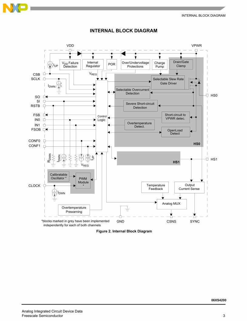
ELECTRICAL CHARACTERISTICSMAXIMUM RATINGS
ELECTRICAL CHARACTERISTICS
MAXIMUM RATINGS
Table 3. Maximum Ratings All voltages are relative to ground unless mentioned otherwise. Exceeding these ratings may cause permanent damage.
Parameter Symbol Maximum ratings Unit
ELECTRICAL RATINGS
VPWR Supply Voltage RangeLoad Dump at 25 °C (500 ms)Reverse Battery at 25 °C
06XS420006XS4200B
Fast Negative Transient Pulses (ISO 7637-2 pulse #1, VPWR = 14 V & Ri = 10 Ohm)
VPWR
58
-28-32-60
V
VDD Supply Voltage Range VDD -0.3 to 5.5 V
Voltage on Input pins(3) (except IN[0:1]) and Output pins(4)(except HS[0:1]) VMAX,LOGIC(3) -0.3 to 5.5 V
Voltage on Fail-safe Output (FSOB) VFSO -0.3 to 58 V
Voltage on SO pin VSO -0.3 to VDD+0.3 V
Voltage (continuous, max. allowable) on IN[0:1] Inputs VIN,MAX 58 V
Voltage (continuous, max. allowable) on output pins (HS [0:1])06XS4200 06XS4200B
VHS[0:1]
-28 to 58-32 to 58
V
Rated Continuous Output Current per channel(5) IHS[0:1] 9.0 A
Maximum allowable energy dissipation per channel and two parallel channels, single-pulse method(6)
ECL [0:1]_SING250
mJ
ESD Voltage(7)
Human Body Model (HBM) for HS[0:1], VPWR and GNDHuman Body Model (HBM) for other pins Charge Device Model (CDM)
Package Corner pins (1, 13, 19, 20)All Other pins
VESD1VESD2
VESD3VESD4
± 8000± 2000
± 750± 500
V
Notes:3. Concerned Input pins are: CONF[0:1], RSTB, SI, SCLK, Clock, and CSB.4. Concerned Output pins are: CSNS, SYNC, and FSB.5. Output current rating valid as long as maximum junction temperature is not exceeded. For computation of the maximum allowable output
current, the thermal resistance of the package & the underlying heatsink must be taken into account 6. Single pulse Energy dissipation, Single-pulse short-circuit method (LL = 0.5 mH, R = 48 mOhm, VPWR = 28 V, TJ = 150 °C initial). 7. ESD testing is performed in accordance with the Human Body Model (HBM) (CZAP = 100 pF, RZAP = 1500 Ohm), and the Charge Device
Model (CDM), Robotic (CZAP = 4.0 pF).
Analog Integrated Circuit Device Data Freescale Semiconductor 7
06XS4200
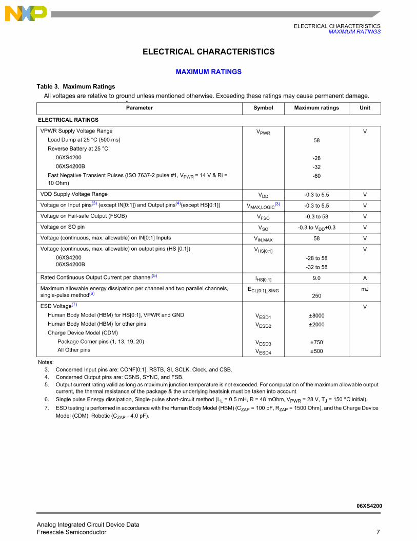
ELECTRICAL CHARACTERISTICSMAXIMUM RATINGS
THERMAL RATINGS
Operating TemperatureAmbientJunction
TA
TJ
- 40 to 125- 40 to 150
°C
Storage Temperature TSTG - 55 to 150 °C
Thermal Resistance / Junction to Case RθJC <1.0 °C/ W
Reflow Peak Temperature on device pins during soldering(8), (9) TSOLDER 260 °C
Notes:8. 10 seconds maximum duration. Not designed for immersion soldering. Exceeding these limits may cause malfunction or permanent
damage to the device. MSL level is specified later.9. Freescale’s Package Reflow capability meets Pb-free requirements for JEDEC standard J-STD-020. For Peak Package Reflow
Temperature and Moisture Sensitivity Levels (MSL), Go to www.freescale.com, search by part number [e.g. remove prefixes/suffixes and enter the core ID to view all orderable parts. (i.e. MC33xxxD enter 33xxx), and review parametrics.
Table 3. Maximum Ratings (continued)All voltages are relative to ground unless mentioned otherwise. Exceeding these ratings may cause permanent damage.
Parameter Symbol Maximum ratings Unit
Analog Integrated Circuit Device Data 8 Freescale Semiconductor
06XS4200

ELECTRICAL CHARACTERISTICSSTATIC ELECTRICAL CHARACTERISTICS
STATIC ELECTRICAL CHARACTERISTICS
Table 4. Static Electrical Characteristics Unless specified otherwise: 8.0 V ≤ VPWR ≤ 36 V, 3.0 V ≤ VDD ≤ 5.5 V, - 40 °C ≤ TA ≤ 125 °C, GND = 0 V. Typical values are
average values evaluated under nominal conditions TA = 25 °C, VPWR = 28 V & VDD = 5.0 V, unless specified otherwise.
parameter Symbol Min Typ Max Unit
SUPPLY ELECTRICAL CHARACTERISTICS
Supply Voltage Range:Full Specification compliant
Extended Mode(10)
VPWR8.06.0
24–
3658
V
VPWR Supply Current, device in wake-up mode, channel On, OpenLoad
Outputs in ON-state, HS[0 : 1] open, IN[0:1] > VIH
IPWR(ON)– 6.5 8.0
mA
VPWR Supply Current, device in wake-up mode (Standby), channel OffOpenLoad in OFF-state Detection Disabled, HS[0 : 1] shorted to ground with VDD = 5.5 V and RSTB > VWAKE
IPWR(SBY)– 6.5 8.0
mA
Sleep State Supply Current VPWR = 24 V, RSTB = IN[0:1] < VWAKE, HS[0 : 1] connected to ground
TA = 25 °C
TA = 125 °C
IPWR(SLEEP)
––
3.0–
10.0 60.0
μA
VDD Supply Voltage VDD(ON) 3.0 – 5.5 V
VDD Supply Current at VDD = 5.5 VNo SPI Communication
8.0 MHz SPI Communication(11)
IDD(ON) ––
–5.0
2.2–
mA
VDD Sleep State Current at VDD = 5.5 V with or without VPWR IDD(SLEEP) – – 5.0 μA
Overvoltage Shutdown Threshold VPWR(OV) 39 42 45.5 V
Overvoltage Shutdown Hysteresis VPWR(OVHYS) 0.2 0.8 1.5 V
Undervoltage Shutdown Threshold(12) VPWR(UV) 5.0 – 6.0 V
VPWR Power-On-Reset (POR) Voltage Threshold(12) VPWR(POR) 2.2 2.6 4.0 V
VDD Power-On-Reset (POR) Voltage Threshold(12) VDD(POR) 1.5 2.0 2.5 V
VDD Supply Failure Voltage Threshold (assumed VPWR > VPWR(UV)) VDD(FAIL) 2.2 2.5 2.8 V
Notes10. In extended mode, availability of several device functions (channel control, value of RDS(ON), overtemperature protection) is guaranteed,
but compliance with the specified values in this document is not. Below 6.0 V, the device is only protected from overheating (thermal shutdown). Above VPWR(OV), the channels can only be turned ON when the overvoltage detection function has been disabled.
11. Typical value guaranteed per design.12. When the device recovers from undervoltage and returns to normal mode (6.0 V < VPWR < 58 V) before the end of the auto-retry period
(see Auto-retry), the device performs normally. When VPWR drops below VPWR(UV), undervoltage is detected (see Undervoltage Fault (Latchable Fault) and EMC Performances).
Analog Integrated Circuit Device Data 9 Freescale Semiconductor
06XS4200

ELECTRICAL CHARACTERISTICSSTATIC ELECTRICAL CHARACTERISTICS
ELECTRICAL CHARACTERISTICS OF THE OUTPUT STAGE (HS0 AND HS1)
ON-Resistance, Drain-to-Source (IHS = 3.0 A, TJ = 25 °C) CSNS_ratio = 0
VPWR = 8.0 V
VPWR = 28 V
VPWR = 36 V
RDS(ON)25
–––
–––
6.06.06.0
mΩ
ON-Resistance, Drain-to-Source (IHS = 3.0 A,TJ = 150 °C) CSNS_ratio = 0
VPWR = 8.0 V
VPWR = 28 V
VPWR = 36 V
RDS(ON)150
–––
–––
121212
mΩ
ON-Resistance, Drain-to-Source difference from one channel to the other in parallel mode (IHS = 1.0 A,TJ = 150 °C) CSNS_ratio = X
ΔRDS(ON)150
-0.7 – +0.7 mΩ
ON-Resistance, Source-Drain (IHS = -3.0 A, TJ = 150 °C, VPWR = -24 V) RSD(ON)150 – – 12 mΩ
Max. detectable wiring length (2.5 mm²) for severe short-circuit detection (see Severe Short-circuit Fault (latchable fault)):
High slew rate selected Medium slew rate selected:Low slew rate selected:
LSHORT
143060
48100200
80170340
cm
Overcurrent Detection thresholds with CSNS_ratio bit = 0 (CSR0) I_OCH1_0
I_OCH2_0
I_OCM1_0
I_OCM2_0
I_OCL1_0
I_OCL2_0
I_OCL3_0
90.058.336.122.215.010.05.0
110.070.043.326.718.012.06.0
128.381.750.631.121.014.07.0
A
Overcurrent Detection thresholds with CSNS_ratio bit = 1(CSR1) I_OCH1_1
I_OCH2_1
I_OCM1_1
I_OCM2_1
I_OCL1_1
I_OCL2_1
I_OCL3_1
30.619.412.07.45.03.31.6
36.723.314.48.96.04.02.0
42.827.216.910.47.04.72.4
A
Output (HS[x]) leakage Current in sleep state (positive value = outgoing)06XS4200
VHS,OFF = 0 V (VHS,OFF = output voltage in OFF state) VHS,OFF = VPWR, device in sleep state (VPWR = 24 V)
06XS4200BVHS,OFF = 0 V (VHS,OFF = output voltage in OFF state) VHS,OFF = VPWR, device in sleep state (VPWR = 24 V) VHS,OFF = VPWR, device in sleep state (VPWR = 36 V)
IOUT_LEAK
–-40.0
–-120
-1400
––
–––
+16+5.0
+16+5.0+5.0
µA
Table 4. Static Electrical Characteristics (continued)Unless specified otherwise: 8.0 V ≤ VPWR ≤ 36 V, 3.0 V ≤ VDD ≤ 5.5 V, - 40 °C ≤ TA ≤ 125 °C, GND = 0 V. Typical values are
average values evaluated under nominal conditions TA = 25 °C, VPWR = 28 V & VDD = 5.0 V, unless specified otherwise.
parameter Symbol Min Typ Max Unit
Analog Integrated Circuit Device Data 10 Freescale Semiconductor
06XS4200

ELECTRICAL CHARACTERISTICSSTATIC ELECTRICAL CHARACTERISTICS
ELECTRICAL CHARACTERISTICS OF THE OUTPUT STAGE (HS0 AND HS1) (CONTINUED)
Output biasing current in off-state (positive value = outgoing) 06XS4200Bwith OL_OFF disabled (worst case VPWR = 36 V, VHS,OFF = 34 V)
Fast slew rate selected Medium slew rate selected Slow slew rate selected With OL_OFF disabled and ECU ground disconnected (VPWR = 32 V)
IOUT_OFF
-770-520-3900.0
-620-420-315
–
-460-310-2401000
µA
Switch Turn-on threshold for supply overvoltage (VPWR -GND) VD_GND(CLAMP) 58 – 66 V
Switch turn-on threshold for drain-source overvoltage (@ IHS = 100 mA) VDS(CLAMP) 58 – 66 V
Switch turn-on threshold for Drain-Source overvoltage difference from one channel to the other in parallel mode (@ IHS = 100 mA)
ΔVDS(CLAMP)
-2.0 – +2.0 V
Current Sensing Ratio(13)
CSNS_ratio bit = 0 (high-current mode)CSNS_ratio bit = 1 (low-current mode)
CSR0
CSR1
––
1/50001/1666.6
––
–
Minimum measurable load current with compensated error(14) < 35% I_LOAD_MIN – – 175 mA
CSNS leakage current in OFF state (CSNSx_en = 0, CSNS_ratio bit_x = 0)
ICSR_LEAK -4.0 – +4.0 µA
Systematic offset error (see Current Sense Errors)06XS420006XS4200B
I_LOAD_ERR_SYS
––
15-22
––
mA
Random offset error I_LOAD_ERR_RAND -360 – 360 mA
CSNS pin current sourcing capability, absolute upper limit ICSNS,MAX 5.15 – – mA
ESR0 Output Current Sensing Error (%, uncompensated(15)) at output Current level (Sense ratio CSR0 selected):
TJ = -40 °C
9.0 A4.5 A2.25 A1.13 A
TJ = 125 °C
9.0 A4.5 A2.25 A1.13 A
TJ = 25 to 125 °C
9.0 A4.5 A2.25 A1.13 A
ESR0_ERR
-13-12-17-31
-10-9.0-12-19
-10-9.0-12-22
––––
––––
––––
13121731
109.01219
109.01222
%
Table 4. Static Electrical Characteristics (continued)Unless specified otherwise: 8.0 V ≤ VPWR ≤ 36 V, 3.0 V ≤ VDD ≤ 5.5 V, - 40 °C ≤ TA ≤ 125 °C, GND = 0 V. Typical values are
average values evaluated under nominal conditions TA = 25 °C, VPWR = 28 V & VDD = 5.0 V, unless specified otherwise.
parameter Symbol Min Typ Max Unit
Analog Integrated Circuit Device Data Freescale Semiconductor 11
06XS4200

ELECTRICAL CHARACTERISTICSSTATIC ELECTRICAL CHARACTERISTICS
ELECTRICAL CHARACTERISTICS OF THE OUTPUT STAGE (HS0 AND HS1) (CONTINUED)
ESR0 Output Current Sensing Error (%, after offset compensation(14)) at output Current level (Sense ratio CSR0 selected):
TJ = -40 °C
9.0 A4.5 A2.25 A1.13 A
TJ = 125 °C
9.0 A4.5 A2.25 A1.13 A
TJ = 25 to 125 °C
9.0 A4.5 A2.25 A1.13 A
ESR0_ERR(Comp)
-10-10-10-10
-9.0-8.0-9.0-9.0
-9.0-8.0-9.0-9.0
––––
––––
––––
10101010
9.08.09.09.0
9.08.09.09.0
%
ESR1 Output Current Sensing Error (%, uncompensated (15)) at output Current level (Sense ratio CSR1 selected):
TJ = -40 °C
2.25 A
TJ = 125 °C
2.25 A
TJ = 25 to 125 °C
2.25 A
ESR1_ERR
-16
-12
-12
–
–
–
16
12
12
%
Notes:13. Current Sense Ratio CSRX = ICSNS / (IHS[x] + I_LOAD_ERR_SYS)
14. See note (15), but with ICSNS_MEAS obtained after compensation of I_LOAD_ERR_RAND (see Activation and Use of Offset Compensation). Further accuracy improvements can be obtained by performing a 1 or 2 point calibration
15. ESRX_ERR = (ICSNS_MEAS / ICSNS_MODEL) - 1, with ICSNS_MODEL = (I(HS[x]) + I_LOAD_ERR_SYS) * CSRX , (I_LOAD_ERR_SYS defined above, see section Current Sense Error Model). With this model, load current becomes: I(HS[x]) = ICSNS / CSRX - I_LOAD_ERR_SYS
Table 4. Static Electrical Characteristics (continued)Unless specified otherwise: 8.0 V ≤ VPWR ≤ 36 V, 3.0 V ≤ VDD ≤ 5.5 V, - 40 °C ≤ TA ≤ 125 °C, GND = 0 V. Typical values are
average values evaluated under nominal conditions TA = 25 °C, VPWR = 28 V & VDD = 5.0 V, unless specified otherwise.
parameter Symbol Min Typ Max Unit
Analog Integrated Circuit Device Data 12 Freescale Semiconductor
06XS4200

ELECTRICAL CHARACTERISTICSSTATIC ELECTRICAL CHARACTERISTICS
ELECTRICAL CHARACTERISTICS OF THE OUTPUT STAGE (HS0 AND HS1) (CONTINUED)
ESR1 Output Current Sensing Error (% after offset compensation(16)) at output Current level (Sense ratio CSR1 selected):
TJ = -40 °C
2.25 A0.75 A0.375 A0.225 A
TJ = 125 °C
2.25 A0.75 A0.375 A0.225 A
TJ = 25 to 125 °C
2.25 A0.75 A0.375 A0.225 A
ESR1_ERR(Comp)
-10-11-18-29
-8.0-10-12-16
-8.0-10-13-21
––––
––––
––––
10111829
8.0101216
8.0101321
%
ESR0 Output Current Sensing Error in parallel mode (%, uncompensated(17)) at outputs Current level (Sense ratio CSR0 selected):
TJ = -40 °C
9.0 A4.5 A
TJ = 125 °C
9.0 A4.5 A
TJ = 25 to 125 °C
9.0 A4.5 A
ESR0_ERR_PAR
-10-11
-8.0-8.0
-8.0-8.0
––
––
––
1011
8.08.0
8.08.0
%
Current Sense Clamping Voltage (condition: R(CSNS) > 10 kOhm) VCL(CSNS) 5.5 – 7.5 V
OpenLoad detection Current threshold in OFF state (18) IOLD(OFF) 30 – 100 μA
OpenLoad Fault Detection Voltage Threshold (18) VOLD(THRES) 4.0 – 5.5 V
Notes:16. See note (17), but with ICSNS_MEAS obtained after compensation of I_LOAD_ERR_RAND (see Activation and Use of Offset Compensation).
Further accuracy improvements can be obtained by performing a 1 or 2 point calibration.17. ESRX_ERR = (ICSNS_MEAS / ICSNS_MODEL) -1, with ICSNS_MODEL = (I(HS[x])+ I_LOAD_ERR_SYS) * CSRX , (I_LOAD_ERR_SYS defined above,
see section Current Sense Error Model). With this model, load current becomes: I(HS[x]) = ICSNS / CSRX - I_LOAD_ERR_SYS18. Minimum required value of OpenLoad impedance for detection of OpenLoad in OFF-state: 200 kΩ.(VOLD(THRES) = VHS @ IOLD(OFF))
Table 4. Static Electrical Characteristics (continued)Unless specified otherwise: 8.0 V ≤ VPWR ≤ 36 V, 3.0 V ≤ VDD ≤ 5.5 V, - 40 °C ≤ TA ≤ 125 °C, GND = 0 V. Typical values are
average values evaluated under nominal conditions TA = 25 °C, VPWR = 28 V & VDD = 5.0 V, unless specified otherwise.
parameter Symbol Min Typ Max Unit
Analog Integrated Circuit Device Data 13 Freescale Semiconductor
06XS4200

ELECTRICAL CHARACTERISTICSSTATIC ELECTRICAL CHARACTERISTICS
ELECTRICAL CHARACTERISTICS OF THE OUTPUT STAGE (HS0 AND HS1) (CONTINUED)
OpenLoad detection Current threshold in ON state (see OpenLoad Detection In On State (OL_ON)):
CSNS_ratio bit = 006XS420006XS4200B
CSNS_ratio bit = 1 (fast slew rate SR[1:0] = 10 mandatory for this function)
IOLD(ON)
200.0135.0
5.0
500.0500.0
7.0
999.9999.9
10
mA
Time period of the periodically activated OpenLoad in ON state detection for CSNS_ratio bit = 1
tOLLED 105 150 195 ms
Output Shorted-to-VPWR Detection Voltage Threshold (channel in OFF state)
VOSD(THRES) VPWR-1.2 VPWR-0.8 VPWR-0.4 V
Switch turn-on threshold for Negative Output Voltages (protects against negative transients) - (measured at IOUT = 100 mA, Channel in OFF state)
06XS420006XS4200B
VCL
-35-38
––
-24-32
V
Switch turn-on threshold for Negative Output Voltages difference from one channel to the other in parallel mode - (measured at IOUT = 100 mA, Channel in OFF state)
ΔVCL
-2.0 – +2.0 V
Switching State (On/Off) discrimination thresholds VHS_TH 0.45*VPWR 0.5*VPWR 0.55*VPWR V
Shutdown temperature (Power MOSFET junction; 6.0 V < VPWR < 58 V) TSD 160 175 190 °C
ELECTRICAL CHARACTERISTICS OF THE CONTROL INTERFACE PINS
Logic Input Voltage, High(19) VIH 2.0 – 5.5 V
Logic Input Voltage, Low(19) VIL -0.3 – 0.8 V
Wake-up Threshold Voltage (IN[0:1] and RSTB)(20) VWAKE 1.0 – 2.2 V
Internal Pull-down Current Source (on Inputs: CLOCK, SCLK and SI)(21) IDWN 5.0 – 20 μA
Internal Pull-up Current Source (input CSB)(22) IUP_CSB 5.0 – 20 μA
Internal Pull-up Current Source (input CONF[0:1])(23) IUP_CONF 25 – 100 μA
Capacitance of SO, FSB and FSOB pins in Tri-state CSO – – 20 pF
Internal Pull-down Resistance (RSTB and IN[0:1]) RDWN 125 250 500 kΩ
Input Capacitance(24) CIN – 4.0 12 pF
Notes19. High and low voltage ranges apply to SI, CSB, SCLK, RSTB, IN[0:1] and CLOCK input signals. The IN[0:1] signals may be derived from
VPWR and can tolerate voltages up to 58 V.20. Voltage above which the device wakes up21. Valid for VSI > 0.8 V and VSCLK > 0.8 V and VCLOCK > 0.8 V. 22. Valid for VCSB < 2.0 V. CSB has an internal pull-up current source derived from VDD23. Pins CONF[0:1] are connected to an internal current source, derived from an internal voltage regulator (VREG ~ 3.0 V).24. Input capacitance of SI, CSB, SCLK, RSTB, IN[0:1], CONF[0:1], and CLOCK pins. This parameter is guaranteed by the manufacturing
process but is not tested in production.
Table 4. Static Electrical Characteristics (continued)Unless specified otherwise: 8.0 V ≤ VPWR ≤ 36 V, 3.0 V ≤ VDD ≤ 5.5 V, - 40 °C ≤ TA ≤ 125 °C, GND = 0 V. Typical values are
average values evaluated under nominal conditions TA = 25 °C, VPWR = 28 V & VDD = 5.0 V, unless specified otherwise.
parameter Symbol Min Typ Max Unit
Analog Integrated Circuit Device Data 14 Freescale Semiconductor
06XS4200

ELECTRICAL CHARACTERISTICSSTATIC ELECTRICAL CHARACTERISTICS
ELECTRICAL CHARACTERISTICS OF THE CONTROL INTERFACE PINS (CONTINUED)
SO High-state Output Voltage(IOH = 1.0 mA)
VSOH
VDD-0.4 – –V
SYNC, SO, FSOB and FSB Low-state Output Voltage(IOL = -1.0 mA)
VSOL
– – 0.4V
SYNC, SO, CSNS, FSOB and FSB Tri-state Leakage Current:(0 V < V(SO) < VDD, or V(FS) or V(SYNC) = 5.5 V, or V(FSO) = 36 V or V(CSNS) = 0 V)
ISO(LEAK)
- 2.0 0 2.0μA
CONF[0:1]: Required values of the External Pull-down ResistorLighting applicationsDC motor applications
RCONF
1.050
––
10Infinite
kΩ
Table 4. Static Electrical Characteristics (continued)Unless specified otherwise: 8.0 V ≤ VPWR ≤ 36 V, 3.0 V ≤ VDD ≤ 5.5 V, - 40 °C ≤ TA ≤ 125 °C, GND = 0 V. Typical values are
average values evaluated under nominal conditions TA = 25 °C, VPWR = 28 V & VDD = 5.0 V, unless specified otherwise.
parameter Symbol Min Typ Max Unit
Analog Integrated Circuit Device Data Freescale Semiconductor 15
06XS4200

ELECTRICAL CHARACTERISTICSDYNAMIC ELECTRICAL CHARACTERISTICS
DYNAMIC ELECTRICAL CHARACTERISTICS
Table 5. Dynamic Electrical Characteristics Unless specified otherwise: 8.0 V ≤ VPWR ≤ 36 V, 3.0 V ≤ VDD ≤ 5.5 V, - 40 °C ≤ TA ≤ 125 °C, GND = 0 V. Typical values are
average values evaluated under nominal conditions TA = 25 °C,VPWR = 28 V & VDD = 5.0 V, unless specified otherwise.
Parameter Symbol Min Typ Max Unit
OUTPUT VOLTAGE SWITCHING CHARACTERISTICS
Rising and falling edge medium slew rate (SR[1:0] = 00)(25)
VPWR = 16 V
VPWR = 28 V
VPWR = 36 V
SRR_00
SRF_00 0.1640.280.34
–––
0.650.790.90
V/μs
Rising edge low slew rate (SR[1:0] = 01)(25)
VPWR = 16 V
VPWR = 28 V
VPWR = 36 V
SRR_01
SRF_01 0.0810.140.17
–––
0.320.3950.45
V/μs
Rising edge high slew rate / SR[1:0] = 10)(25)
VPWR = 16 V
VPWR = 28 V
VPWR = 36 V
SRR_10
SRF_10 0.290.550.68
–––
1.301.581.80
V/μs
Rising/Falling edge slew rate matching per channel 16 V < VPWR < 36 V
SRR/SRF0.75 – 1.2
Edge slew rate difference from one channel to the other in parallel mode(25)
16 V < VPWR < 36 V
SR[1:0] = 00SR[1:0] = 01SR[1:0] = 10
ΔSR
-0.1-0.06-0.14
0.00.00.0
+0.1+0.06+0.14
V/μs
Output Turn-ON and Turn-OFF Delays (medium slew rate: SR[1:0] = 00)(26)
16 V < VPWR < 36 Vt DLY_00
39 - 145μs
Output Turn-ON and Turn-OFF Delays (low slew rate / SR[1:0] = 01)(26)
16 V < VPWR < 36 Vt DLY_01
50 - 280μs
Output Turn-ON and Turn-OFF Delays (high slew rate / SR[1:0] = 10)(26)
16 V < VPWR < 36 Vt DLY_10
22 - 80μs
Turn-ON and Turn-OFF Delay time matching per channel (t DLY(ON) - t DLY(OFF)) f PWM = 400 Hz, 16 V < VPWR < 36 V, duty cycle on IN[x] = 50 %, SR[1:0] = 00
Δ t RF_00
-25 0.0 25μs
Turn-ON and Turn-OFF Delay time matching per channel (t DLY(ON) - t DLY(OFF)) f PWM = 200 Hz, 16 V < VPWR < 36 V, duty cycle on IN[x] = 50 %, SR[1:0] = 01
06XS420006XS4200B
Δ t RF_01
-60-90
0.00.0
6090
μs
Notes25. Rising and Falling edge slew rates specified for a 20% to 80% voltage variation on a 10.0 Ω resistive load (see Figure 4).26. Turn-on delay time measured as delay between a rising edge of the channel control signal (IN[0 : 1] = 1) and the associated rising edge
of the output voltage up to: VHS[0 : 1] = VPWR / 2 (where RL = 5.0 Ω). Turn-OFF delay time is measured as time between a falling edge of the channel control signal (IN[0 : 1] = 0) and the associated falling edge of the output voltage up to the instant at which: VHS[0 : 1] = VPWR / 2 (RL = 10.0 Ohm.
Analog Integrated Circuit Device Data 16 Freescale Semiconductor
06XS4200
ELECTRICAL CHARACTERISTICSDYNAMIC ELECTRICAL CHARACTERISTICS
SWITCHING CHARACTERISTICS (CONTINUED)
Turn-ON and Turn-OFF Delay time matching per channel (t DLY(ON) - t DLY(OFF)) f PWM = 1.0 kHz, 16 V < VPWR < 36 V, duty cycle on IN[x] = 50 %, SR[1:0] = 10
Δ t RF_10
-13 0.0 13μs
Delay time difference from one channel to the other in parallel mode(27)
16 V < VPWR < 36 V
SR[1:0] = 0006XS420006XS4200B
SR[1:0] = 0106XS420006XS4200B
SR[1:0] = 10
Δ t(DLY)
-21-25
-41-50-12
0.00.0
0.00.00.0
2125
415012
μs
Fault Detection Delay Time(28) tFAULT – 5.0 8.0 μs
Output Shutdown Delay Time(29) tDETECT – 12.0 17 μs
Current sense output settling Time for SR[1:0] = 00 (medium slew rate) (30)
16 V < VPWR < 36 Vt CSNSVAL_00
0.0 - 200μs
Current sense output settling Time for SR[1:0] = 01(low slew rate)(30)
16 V < VPWR < 36 Vt CSNSVAL_01
0.0 - 315 μs
Current sense output settling Time for SR[1:0] = 10 (high slew rate)(30)
16 V < VPWR < 36 Vt CSNSVAL_10
0.0 - 165 μs
SYNC output signal delay for SR[1:0] = 00 (medium SR) (30)
06XS420006XS4200B
t SYNCVAL_00
4650
--
155160
μs
SYNC output signal delay for SR[1:0] = 01 (low SR)(30)
06XS420006XS4200B
t SYNCVAL_01
5580
--
280320
μs
SYNC output signal delay for SR[1:0] = 10 (high SR) (30) t SYNCVAL_10 22 - 80 μs
Recommended sync_to_read delay SR[1:0] = 00 (medium slew rate) (30) t SYNREAD_00 0.0 - 200 µs
Recommended sync_to_read delay SR[1:0] = 01 (low slew rate) (30) t SYNREAD_01 0.0 - 200 µs
Recommended sync_to_read delay SR[1:0] = 10 (high slew rate) (30) t SYNREAD_10 0.0 - 200 µs
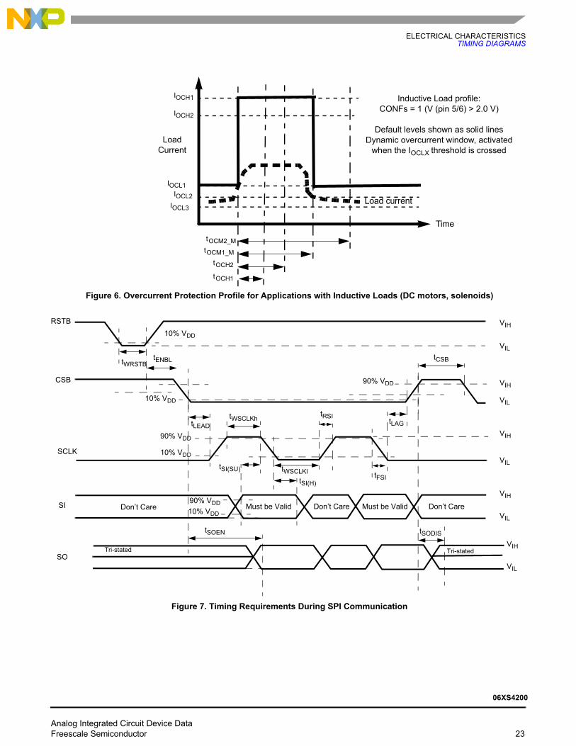
Upper overcurrent threshold duration tOCH1
tOCH2
6.012.0
8.617.2
11.222.4
ms
Notes:27. Rising and Falling edge slew rates specified for a 20% to 80% voltage variation on a 10.0 Ω resistive load (see Figure 4).28. Time required to detect and report the fault to the FSB pin.29. Time required to switch off the channel after detection of overtemperature (OT), overcurrent (OC), SC or UV error (time measured
between start of the negative edge on the FSB pin and the falling edge on the output voltage until V(HS[0:1)) = 50% of VPWR30. Settling time ( = t CSNSVAL_XX), SYNC output signal delay ( = t SYNCVAL_XX) and Read-out delay ( = t SYNREAD_XX) are defined for a
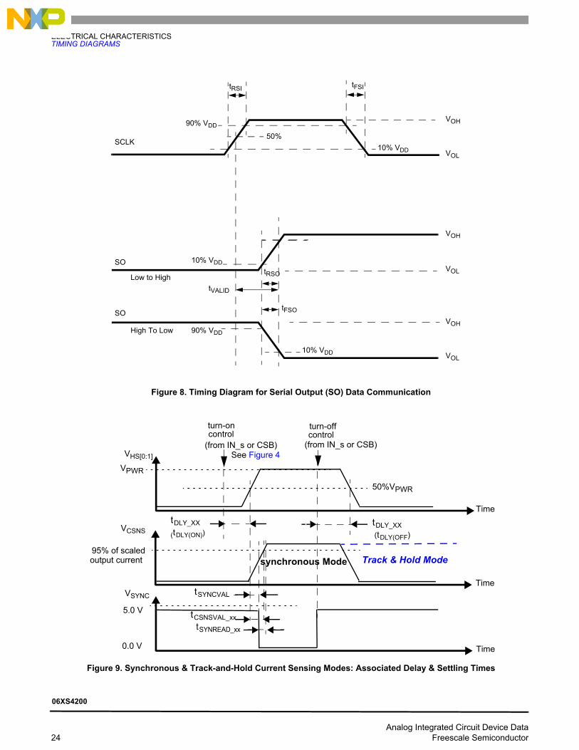
stepped load current (100 mA< I(LOAD)<IOCLX A FOR CSNS_RATIO_S = 1, AND 300 mA< I(LOAD)<IOCLX A_0 FOR CSNS_RATIO_S = 0). (see Figure 9 and Output Current Monitoring (CSNS)).
Table 5. Dynamic Electrical Characteristics (continued)Unless specified otherwise: 8.0 V ≤ VPWR ≤ 36 V, 3.0 V ≤ VDD ≤ 5.5 V, - 40 °C ≤ TA ≤ 125 °C, GND = 0 V. Typical values are
average values evaluated under nominal conditions TA = 25 °C,VPWR = 28 V & VDD = 5.0 V, unless specified otherwise.
Parameter Symbol Min Typ Max Unit
Analog Integrated Circuit Device Data Freescale Semiconductor 17
06XS4200

ELECTRICAL CHARACTERISTICSDYNAMIC ELECTRICAL CHARACTERISTICS
SWITCHING CHARACTERISTICS (CONTINUED)
Medium overcurrent threshold duration (CONF = 0; Lighting Profile) tOCM1_L
tOCM2_L
4896
67137
87178
ms
Medium overcurrent threshold duration (CONF = 1; DC motor Profile) tOCM1_M
tOCM2_M
150301
214429
278557
ms
FREQUENCY & PWM DUTY CYCLE RANGES (31)(protections fully operational, see Protective Functions)
Switching Frequency range - Direct Inputs fCONTROL 0.0 – 1000 Hz
Switching Frequency range - External clock with internal PWM (recommended) fPWM_EXT 20 – 1000 Hz
Switching Frequency range - Internal clock with internal PWM (recommended) fPWM_INT 60 – 1000 Hz
Duty Cycle range RCONTROL 0.0 – 100 %
Notes:31. In Direct Input mode, the lower frequency limit is 0 Hz with RSTB = 5.0 V and 4.0 Hz with RSTB = 0 V. Duty-cycle applies to instants at
which VHS = 50 % VPWR. For low duty-cycle values, the effective value also depends on the value of the selected slew rate.
Table 5. Dynamic Electrical Characteristics (continued)Unless specified otherwise: 8.0 V ≤ VPWR ≤ 36 V, 3.0 V ≤ VDD ≤ 5.5 V, - 40 °C ≤ TA ≤ 125 °C, GND = 0 V. Typical values are
average values evaluated under nominal conditions TA = 25 °C,VPWR = 28 V & VDD = 5.0 V, unless specified otherwise.
Parameter Symbol Min Typ Max Unit
Analog Integrated Circuit Device Data 18 Freescale Semiconductor
06XS4200
ELECTRICAL CHARACTERISTICSDYNAMIC ELECTRICAL CHARACTERISTICS
AVAILABILITY DIAGNOSTIC FUNCTIONS OVER DUTY-CYCLE AND SWITCHING FREQUENCY(PROTECTIONS & DIAGNOSTICS BOTH FULLY OPERATIONAL, SEE DIAGNOSTIC FEATURES FOR THE EXACT BOUNDARY VALUES)
Available Duty Cycle Range, fPWM = 1.0 kHz high slew rate, PWM mode(32)
OL_OFF
OL_ON
OS
RPWM_1K_H
0.0350.0
–––
6210090
%
Available Duty Cycle Range, fPWM = 400 Hz, medium slew rate, PWM mode(32)
OL_OFF
OL_ON
OS
RPWM_400_M
0.0210.0
–––
8110088
%
Available Duty Cycle Range, fPWM = 400 Hz, high slew rate, PWM mode(32)
OL_OFF
OL_ON
OS
RPWM_400_H
0.0140.0
–––
8410095
%
Available Duty Cycle Range, fPWM = 200 Hz, low slew rate mode, PWM mode(32)
OL_OFF
OL_ON
OS
RPWM_200_L
0.0150.0
–––
8610093
%
Available Duty Cycle Range, fPWM = 200 Hz, medium slew rate, PWM mode(32)
OL_OFF
OL_ON
OS
RPWM_200_M
0.0110.0
–––
9010094
%
Available Duty Cycle Range, fPWM = 100 Hz in low slew rate, PWM mode(32)
OL_OFF
OL_ON
OS
RPWM_100_L
0.08.00.0
–––
9310096
%
Deviation of the internal clock PWM frequency after Calibration(33) AFPWM(CAL) -10 – +10 %
Default output frequency when using an uncalibrated oscillator fPWM(0) 280 400 520 Hz
Minimal required Low Time during Calibration of the Internal Clock through CSB t CSB(MIN) 1.0 1.5 2.0 μs
Maximal allowed Low Time during Calibration of the Internal Clock through CSB t CSB(MAX) 70 100 130 μs
Recommended external Clock Frequency Range (external clock/PWM Module) fCLOCK 15 – 512 kHz
Upper detection threshold for external clock frequency monitoring f CLOCK(MAX) 512 730 930 kHz
Lower detection threshold for external clock frequency monitoring f CLOCK(MIN) 5.0 7.0 10 kHz
Notes32. Actually, the device can be operated outside the specified duty cycle and frequency ranges (basic protective functions OC, SC, UV, OV,
OT remain active) but the availability of the diagnostic functions OL_ON, OL_OFF, OS is affected.33. Values guaranteed from 60 Hz to 1.0 kHz (recommended switching frequency range for internal clock operation).
Table 5. Dynamic Electrical Characteristics (continued)Unless specified otherwise: 8.0 V ≤ VPWR ≤ 36 V, 3.0 V ≤ VDD ≤ 5.5 V, - 40 °C ≤ TA ≤ 125 °C, GND = 0 V. Typical values are
average values evaluated under nominal conditions TA = 25 °C,VPWR = 28 V & VDD = 5.0 V, unless specified otherwise.
Parameter Symbol Min Typ Max Unit
Analog Integrated Circuit Device Data Freescale Semiconductor 19
06XS4200

ELECTRICAL CHARACTERISTICSDYNAMIC ELECTRICAL CHARACTERISTICS
TIMING: SPI PORT, IN[0]/ IN[1] SIGNALS & AUTORETRY
Required Low time allowing delatching or triggering sleep mode (direct input mode) tIN 175 250 325 ms
Watchdog Timeout for entering Fail-safe Mode due to loss of SPI contact(34) t WDTO 217 310 400 ms
Auto-Retry Repetition Period (when activated):Auto_period bits = 00 Auto_period bits = 01 Auto_period bits = 10 Auto_period bits = 11
tAUTO_00tAUTO_01tAUTO_10tAUTO_11
10552.526.213.1
15075
37.517.7
19597.547.824.4
ms
GND PIN TEMPERATURE SENSING FUNCTION
Thermal Prewarning Detection Threshold(35) TOTWAR 110 125 140 °C
Temperature Sensing output voltage @ TA = 25 °C (470 Ω < RCSNS < 10 kΩ) TFEED 918 1078 1238 mV
Gain Temperature Sensing output @ TA = 25 °C (470 Ω < RCSNS < 10 kΩ)(35) DTFEED 10.7 11.1 11.5 mV/°C
Temperature Sensing Error, range [-40 °C, 150 °C], default(35) TFEED_ERROR -15 – +15 °C
Temperature Sensing Error, [-40 °C, 150 °C] after 1 point calibration @ 25 °C(35) TFEED_ERROR_CAL
-5.0 – +5.0 °C
Notes34. Only when the WD_dis bit set to logic [0] (default). Watchdog timeout defined from the rising edge on RST to rising edge HS[0,1]35. Values were obtained by lab characterization.
Table 5. Dynamic Electrical Characteristics (continued)Unless specified otherwise: 8.0 V ≤ VPWR ≤ 36 V, 3.0 V ≤ VDD ≤ 5.5 V, - 40 °C ≤ TA ≤ 125 °C, GND = 0 V. Typical values are
average values evaluated under nominal conditions TA = 25 °C,VPWR = 28 V & VDD = 5.0 V, unless specified otherwise.
Parameter Symbol Min Typ Max Unit
Analog Integrated Circuit Device Data 20 Freescale Semiconductor
06XS4200
ELECTRICAL CHARACTERISTICSDYNAMIC ELECTRICAL CHARACTERISTICS
SPI INTERFACE ELECTRICAL CHARACTERISTICS(36)
Maximum Operating Frequency of the Serial Peripheral Interface (SPI)(37) f SPI – – 8.0 MHz
Required Low-state Duration for reset RSTB(38) t WRSTB 10 – – μs
Required duration from the Rising to the Falling Edge of CSB (Required Setup Time)(39)
t CSB 1.0 – – μs
Rising Edge of RSTB to Falling Edge of CSB (Required Setup Time)(39) t ENBL 5.0 – – μs
Falling Edge of CSB to Rising Edge of SCLK (Required Setup Time)(39) t LEAD 500 – – ns
Falling Edge of SCLK to Rising Edge of CSB (Required Setup lag Time)(39) t LAG 60 – – ns
Required High-state Duration of SCLK (Required Setup Time)(39) t WSCLKh 50 – – ns
Required Low-state Duration of SCLK (Required Setup Time)(39) t WSCLKl 50 – – ns
SI to Falling Edge of SCLK (Required Setup Time)(40) t SI (SU) 15 – – ns
Falling Edge of SCLK to SI (Required hold Time of the SI signal)(40) t SI (H) 30 – – ns
SO Rise TimeCL = 80 pF
t RSO – – 20 ns
SO Fall Time CL = 80 pF
t FSO – – 20 ns
SI, CSB, SCLK, Max. Rise Time allowing operation at fSPI = 8.0 MHz(40) t RSI – – 11 ns
SI, CSB, SCLK, Max. Fall Time allowing operation at fSPI = 8.0 MHz(40) t FSI – – 11 ns
Time from Rising Edge of SCLK to reach a valid level at the SO pin(41) tVALID – – 44 ns
Time from Falling Edge of CSB to reach low-impedance on SO (access time)(42) t SOEN – – 30 ns
Time from Rising Edge of CSB to reach high-impedance on SO pin (turn off time) t SODIS 30 ns
Notes:36. Parameters guaranteed by design. It is recommended to tie unused SPI-pins to GND by resistors 1.0 k <R <10 k37. For clock frequencies > 4.0 MHz, series resistors on the SPI pins should preferably be removed. Otherwise, 470 pF (VMAX. > 40 V)
ceramic speed-up capacitors in parallel with the >8.0 kΩ input resistors are required on pins SCLK, SI, SO, CS38. RSTB low duration is defined as the minimum time required to switch off the channel when previously put ON in SPI mode (direct inputs
inactive).39. Minimum setup time required for the device is the minimum required time that the microcontroller must wait or remain in a given state.40. Rise and Fall time of incoming SI, CSB, and SCLK signals.41. Time required for output data to be available for use at SO, measured with a 80 pF capacitive load.42. Time required for output data to be terminated at SO measured without a series resistor connected CSB.
Table 5. Dynamic Electrical Characteristics (continued)Unless specified otherwise: 8.0 V ≤ VPWR ≤ 36 V, 3.0 V ≤ VDD ≤ 5.5 V, - 40 °C ≤ TA ≤ 125 °C, GND = 0 V. Typical values are
average values evaluated under nominal conditions TA = 25 °C,VPWR = 28 V & VDD = 5.0 V, unless specified otherwise.
Parameter Symbol Min Typ Max Unit
Analog Integrated Circuit Device Data Freescale Semiconductor 21
06XS4200
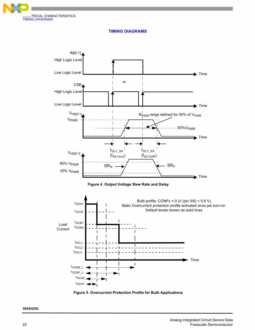
ELECTRICAL CHARACTERISTICSTIMING DIAGRAMS
TIMING DIAGRAMS
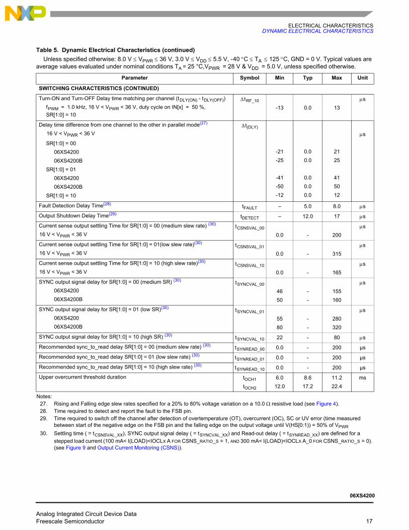
Figure 4. Output Voltage Slew Rate and Delay
Figure 5. Overcurrent Protection Profile for Bulb Applications
VPWR
VHS[0:1]
tDLY_XX tDLY_XX
Low Logic Level
80% VPWR
20% VPWR
SRFSRR
50%VPWR
RPWM range defined for 50% of VPWR
CSB
High Logic Level
VHS[0:1]
Time
Time
Time
Low Logic Level
IN[0:1]
High Logic Level
Time
or
(tDLY(on)) (tDLY(off))
IOCH1
t OCM2_Lt OCM1_L
t OCH1
Time
Load Current
IOCH2
IOCM1
IOCL1IOCL2
IOCM2
t OCH2
Bulb profile: CONFs = 0 (V (pin 5/6) < 0.8 V).Static Overcurrent protection profile activated once per turn-on.
Default levels shown as solid lines
IOCL3
Analog Integrated Circuit Device Data 22 Freescale Semiconductor
06XS4200
ELECTRICAL CHARACTERISTICSTIMING DIAGRAMS
Figure 6. Overcurrent Protection Profile for Applications with Inductive Loads (DC motors, solenoids)
Figure 7. Timing Requirements During SPI Communication
IOCH1
t OCM2_Mt OCM1_M
t OCH1
Time
Load Current
IOCH2
IOCL1IOCL2
t OCH2
Inductive Load profile:CONFs = 1 (V (pin 5/6) > 2.0 V)
Default levels shown as solid linesDynamic overcurrent window, activated
when the IOCLX threshold is crossed
Load currentIOCL3
RSTB
CSB
SCLK
SI Don’t CareMust be Valid Don’t Care
VIH
VIL
tWRSTB
VIH
VIL
VIH
VIL
VIH
VIL
Must be Valid
tENBL
10% VDD
10% VDD
tLEADtWSCLKh
90% VDD
10% VDD
tRSI
90% VDD
tCSB
tLAG
tFSItWSCLKl
tSI(SU)
tSI(H)
90% VDD10% VDD
Don’t Care
VIH
VIL
SO
tSOEN
Tri-stated Tri-stated
tSODIS
Analog Integrated Circuit Device Data Freescale Semiconductor 23
06XS4200
ELECTRICAL CHARACTERISTICSTIMING DIAGRAMS
Figure 8. Timing Diagram for Serial Output (SO) Data Communication
Figure 9. Synchronous & Track-and-Hold Current Sensing Modes: Associated Delay & Settling Times
SCLK
SO
VOH
VOL
tVALID
90% VDD
10% VDD
SO
High To Low
Low to HighVOL
VOL
VOH
VOH
tRSI tFSI
50%
10% VDD
90% VDD
tRSO
tFSO
10% VDD
VPWR
VHS[0:1]
tDLY_XX tDLY_XX
50%VPWR
Time
turn-on
VCSNS
Time
95% of scaled
Time
5.0 V
0.0 V
VSYNC
turn-off controlcontrol
tCSNSVAL_xx
tSYNCVAL
output current Track & Hold Modesynchronous Mode
(tDLY(ON)) (tDLY(OFF)
(from IN_s or CSB) (from IN_s or CSB)
tSYNREAD_xx
See Figure 4
Analog Integrated Circuit Device Data 24 Freescale Semiconductor
06XS4200

FUNCTIONAL DESCRIPTIONINTRODUCTION
FUNCTIONAL DESCRIPTION
INTRODUCTION
The 06XS4200 is a two-channel, 24 V high-side switch with integrated control and diagnostics designed for truck, bus, and industrial applications. The device provides a high number of protective functions. Both low RDS(on) channels (< 6.0 mOhm) can independently drive various load types like light bulbs, solenoid actuators, or DC motors. Device control and diagnostics are configured through a 16-bit SPI port with daisy chain capability.
Independently programmable output voltage slew rates allow satisfying electromagnetic compatibility (EMC) requirements.
Both channels can independently be operated in several different switching modes: internal clock, internal PWM mode (fully autonomous operation), external clock, and direct control switching mode.
Current sensing with an adjustable ratio is available on both channels, allowing both high-current (bulbs) and low-
current (LED) monitoring. By activating the Track & Hold mode, current monitoring can be performed during the switch-Off phase. This allows random access to the current sense functionality. A patented offset compensation technique further enhances current sense accuracy.
To avoid turning off during inrush current, while being able to monitor it, the device features a dynamic overcurrent threshold profile. For bulbs, this profile is a stair function with stages of which the height and width are programmable through the SPI port. DC motors can be protected from overheating by activating a specific window-shaped overcurrent profile that allows stall currents of limited duration.
Whenever communication with the external micro-controller is lost, the device enters Fail-safe Operation mode, but remains operational, controllable and protected.
PIN ASSIGNMENT AND FUNCTIONS
Functions and register bits that are implemented independently for both channels have extension “_s”. Max. ratings of the pins are given in Table 3.
OUTPUT CURRENT MONITORING (CSNS)The CSNS pin allows independent current monitoring of
channel 0 or channel 1 up to the steady-state overcurrent threshold. It can also be used to sense the device temperature. The different functions are selected by setting bits CSNS1_en and CSNS0_en to the appropriate value (Table 12). When the CSNS pin is sensed during switch-off in the (optional) track & hold mode, it outputs the scaled value of the load current as it was just before turn-Off. When several devices share the same pull-down resistor, the CSNS pins of unused devices must be tri-stated. This is accomplished by setting CSNS0_en = 0 and CSNS1_en = 0 in the GCR register. Settling time (tCSNSVAL_XX) is defined as the time between the instant at the middle of the output voltage’s rising edge (HS[0:1] = 50% of VPWR), and the instant at which the voltage on the CSNS-pin has settled to ±5.0% of its final value. Anytime an overcurrent window is active, the CSNS pin is disabled (see Overcurrent Detection on Resistive and Inductive Loads). The current and temperature sensing functions are unavailable in Fail-safe mode and in Normal mode when operating without the VDD supply voltage. In order to generate a voltage output, a pull-down resistor is required (R(CSNS) = 1.0 kOhm typ. and 470 < R(CSNS) < 10 k). When the current sense resistor connected to the CSNS pin is disconnected, the CSNS voltage is clamped to VCL(CSNS). The CSNS pin can source currents up to about 5.6 mA.
CURRENT SENSE SYNCHRONIZATION (SYNC)To synchronize current sensing with an external process,
the SYNC signal can be connected to a digital input of an external MCU. SYNC is asserted logic low when the current sense signal is accurate and ready to be read. The current sense signal on the CSNS pin has the specified accuracy tSYNREAD_XX seconds after the falling edge on the SYNC pin (Figure 9) and remains valid until a rising edge is generated. The rising edge that is generated by the SYNC pin at the turn-OFF instant (internal or external) may also be used to implement synchronization with the external MCU. Parameter tSYNCVAL_XX is defined as the time between the instant at the middle of the output-voltage rising edge (HS[0:1] = 50% of VPWR), and the instant at which the voltage on the SYNC-pin drops below 0.4 V (VSOL). The SYNC pins of different devices can be connected together to save micro-controller input channels. However, in this configuration, the CSNS function of only one device should be active at a time. Otherwise, the MCU does not determine the origin of the SYNC signal. The SYNC pin is open drain and requires an external pull-up resistor to VDD.
DIRECT CONTROL INPUTS (IN0 AND IN1)The IN[0:1] pins allow direct control of both channels. A
logic [0] level turns off the channel and a logic[1] level turns it on (Channel Control in Normal Mode). When the device is in Sleep mode, a transition from logic 0 to logic 1 on any of these pins wake it up (Sleep Mode). If it is desired to automatically turn on the channels after a transition to Fail-safe mode, inputs IN[0] and IN[1] must be externally connected to the VPWR pin by a pull-up resistor (e.g. 10 kOhm typ.). However, this prevents the device from going
Analog Integrated Circuit Device Data Freescale Semiconductor 25
06XS4200

FUNCTIONAL DESCRIPTIONPIN ASSIGNMENT AND FUNCTIONS
into Sleep mode. Both IN pins are internally connected to a pull-down resistor.
CONFIGURATION INPUTS (CONF0 AND CONF1)The CONF[0 :1] input pins allow configuring both channels
for the appropriate load type. CONF = 0 activates the bulb overcurrent protection profile, and CONF = 1 the DC motor profile. These inputs are connected to an internal voltage regulator of 3.3 V by an internal pull-up current source IUP. Therefore, CONF = 1 is the default value when these pins are disconnected. Details on how to configure the channels are given in the table Overcurrent Profile Selection.
FAULT STATUS (FSB)This open-drain output is asserted low when any of the
following faults occurs (see Fault Mode): overcurrent (OC), overtemperature (OT), Output connected to VPWR, Severe short-circuit (SC), OpenLoad in ON state (OL_ON), OpenLoad in OFF state (OL_OFF), External Clock-fail (CLOCK_fail), overvoltage (OV), and undervoltage (UV). Each fault type has its own assigned bit inside the STATR, FAULTR_s, or DIAGR_s register. Fault type identification and fault bit reset are accomplished by reading out these registers. They are part of the SO register (Table 13) and are accessed through the SPI port.
PWM CLOCK (CLOCK)This pin is the input for an external clock signal that
controls the internal PWM module.The clock signal is monitored by the device. The PWM module controls ON-time and turn-ON delay of the selected channels. The CLOCK pin should not be confused with the SCLK pin, which is the clock pin of the SPI interface. CLOCK has an internal pull-down current source (IDWN) to GND.
RESET (RSTB)All SPI register contents are reset when RSTB = 0. When
RSTB = 0, the device returns to Sleep mode tIN sec. after the last falling edge of the last active IN[0:1] signal. As long as the Reset input (RSTB pin) is at logic 0 and both direct input states are low, the device remains in Sleep mode (Channel configuration through the SPI). A 0-to-1 transition on RSTB wakes up the device and starts a watchdog timer to check the continuous presence of the SPI signals. To do this, the device monitors the contents of the first bit (WDIN bit) of all SPI words following that transition (regardless the register it is contained in). When this contents is not alternated within a duration tWDTO, SPI communication is considered lost, and Fail-safe mode is entered (Entering Fail-safe Mode). RSTB is internally pulled-down to GND by resistor RDWN.
CHIP SELECT (CSB)Data communication over the SPI port is enabled when the
CSB pin is in the logic [0] state. Data from the Input Shift registers are locked in the addressed SI registers on the rising edge of CSB. The device transfers the contents of one of the 8 internal registers to the SO register on the falling
edge of CSB. The SO output driver is enabled when CSB is logic [0]. CSB should transition from a logic [1] to a logic [0] state only when SCLK is at logic [0] (Figure 7 and Figure 8). CSB is internally pulled up to VDD through IUP.
SPI SERIAL CLOCK (SCLK)The SCLK pin clocks the SPI data communication of the
device. The serial input pin (SI) transfers data to the SI shift registers on the falling edge of the SCLK signal while data in the SO registers are transferred to the SO pin on the rising edge of the SCLK signal. The SCLK pin must be in the low state when CSB makes any transition. For this reason, it is recommended to have the SCLK pin in the logic [0] state when the device is not accessed (CSB is at logic [1]). When CSB is set to logic [1], signals at the SCLK and SI pins are ignored and the SO output is tri-stated (high-impedance). The SCLK pin is connected to an internal pull-down current source IDWN.
SERIAL INPUT (SI)Serial input (SI) data bits are shifted in at this pin. SI data
is read on the falling edge of SCLK. 16-bit data packages are required on the SI pin (see Figure 7), starting with bit D15 (MSB) and ending with D0 (LSB). All the internal device registers are addressed and controlled by a 4-bit address (D9-D12) described in Table 11. Register addresses and function attribution are described in Table 12. The SI pin is internally connected to a pull-down current source, IDWN.
SUPPLY OF THE DIGITAL CIRCUITRY (VDD)This pin supplies the SPI circuit (3.3 V or 5.0 V). When
lost, all circuitry becomes supplied by a VPWR derived voltage, except the SPI’s SO shift-register that can no longer be read.
GROUND (GND)This is the GND pin common for both the SPI and the other
circuitry.
POSITIVE SUPPLY PIN (VPWR)This pin is the positive supply and the common input pin of
both switches. A 100 nF ceramic capacitor must be connected between VPWR and GND, close to the device. In addition, it is recommended to put a ceramic capacitor of at least 1.0 µF in parallel with this 100 nF capacitor.
SERIAL OUTPUT (SO)The SO pin is a tri-stateable output pin that conveys data
from one of the 13 internal SO registers or from the previous SI register to the outside world. The SO pin remains in a high-impedance state (tri-state) until the CSB pin becomes logic [0]. It then transfers the SPI data (device state, configuration, fault information). The SO pin changes state at the rising edge of the SCLK signal. For daisy-chaining, it can be read out on the falling edge of SCLK. VDD must be present
Analog Integrated Circuit Device Data 26 Freescale Semiconductor
06XS4200

FUNCTIONAL DESCRIPTIONFUNCTIONAL INTERNAL BLOCK DESCRIPTION
before the SO registers can be read. The SO register assignment is described in Table 13.
POWER SWITCH OUTPUT PINS (HS0 AND HS1)HS0 and HS1 are the output pins of the power switches, to
be connected to the loads. A ceramic capacitor (< = 22 nF (+/
- 20%) is recommended between these pins and GND for optimal EMC performances.
FAIL-SAFE OUTPUT (FSOB)This pin (active low) is used to indicate loss of SPI
communication or loss of SPI supply voltage, VDD. This open-drain output requires an external pull-up resistor to VPWR.
FUNCTIONAL INTERNAL BLOCK DESCRIPTION
POWER SUPPLYThe device operates with supply voltages from 6.0 to 58 V
(VPWR), but is full spec. compliant between 8.0 and 36 V. The VPWR pin supplies power to the internal regulator, analog, and logic circuit blocks. The VDD pin (5.0 V typ.) supplies the output register of the Serial Peripheral Interface (SPI). Consequently, the SPI registers cannot be read without presence of VDD. The employed IC architecture guarantees a low quiescent current in Sleep mode.
SWITCH OUTPUT PINS HS0 & HS1HS0 and HS1 are the output pins of the power switches.
Both channels are protected against various kinds of short-circuits and have active clamp circuitry that may be activated when switching off inductive loads. Many protective and diagnostic functions are available. For large inductive loads, it is recommended to use a freewheeling diode. The device can be configured to control the output switches in parallel, which guarantees good switching synchronization.
COMMUNICATION INTERFACE AND DEVICE CONTROL
In Normal mode the output channels can either be controlled by the direct inputs or by the internal PWM module, which is configured by the SPI register settings. For bidirectional SPI communication, VDD has to be in the authorized range. Failure diagnostics and configuration are also performed through the SPI port. The reported failure types are: OpenLoad, short-circuit to battery, severe short-circuit to ground, overcurrent, overtemperature, clock-fail, undervoltage, and overvoltage. The SPI port can be supplied either by a 5.0 V or by a 3.3 V voltage supply. For direct input control, VDD is not required.
A Pulse Width Modulation (PWM) circuit allows driving loads at frequencies up to 1.0 kHz from an external or an internal clock. SPI communication is required to set these options.
POWER SUPPLY
MCU INTERFACE andOUTPUT CONTROL
SPI INTERFACE
PARALLEL CONTROLINPUTS
PWM CONTROLLER
SELF-PROTECTED
High-sideSWITCHES
HS0-HS1
MCUINTERFACE
internal regulator
Analog Integrated Circuit Device Data Freescale Semiconductor 27
06XS4200

FUNCTIONAL DEVICE OPERATIONOPERATION AND OPERATING MODES
FUNCTIONAL DEVICE OPERATION
OPERATION AND OPERATING MODES
The device possesses two high-side switches (channels) each of which can be controlled independently. The device has four fundamental operating modes: Sleep, Normal, Fail-safe, and Fault mode, as shown in Table 6.
Each channel can be controlled in three different ways in Normal mode: by a signal on the Direct Input pin, by an internal clock signal (autonomous operation) or by an external clock signal. For bidirectional SPI communication, a second supply voltage is required (VDD = 5.0 V or 3.3 V). When only the direct inputs IN[x] are used, VDD isn’t required.
DEVICE START-UP SEQUENCETo put the device in a known configuration and guarantee
predictable behavior, the device must undergo a wake-up sequence. However, it should not be woken up earlier than the moment at which VPWR has exceeded its undervoltage threshold, VPWR(UV), and VDD has exceeded its supply failure threshold, VDD(FAIL). In applications using the SPI port, the device is typically put in wake mode by setting RSTB = 1. Wake-up of applications with direct input control can be achieved by having signals IN_ON[0] = 1 or IN_ON[1 ] = 1 (see Figure 10). After wake-up, all SPI register contents are reset (as defined in Table 12 and Table 13) and Normal mode is entered. All the device functions are available 50 µs later (typically).
If the start-up sequence is not performed at device start-up, its configuration may be undetermined and correct operation is not guaranteed. In situations where the above described start-up sequence can not be performed, it is recommended to generate a wake-up event after the moment VPWR has reached the undervoltage threshold.
CHANNEL CONFIGURATION THROUGH THE SPI
Setting the Channel ConfigurationThe channel configuration is determined by the contents of
the pulse-width (PWMR_s), the configuration (CONFR_s) and the overcurrent (OCR_s) registers. They allow setting, among others, the following parameters: duty-cycle, delay, Slew Rate, PWM enable (PWM_en), clock selection (CLOCK_sel), prescaler (PR), and direct_input disable (DIR_dis). Extension “_s” means that these registers exist for each of both channels. Function assignment is described in detail in the section SI Register Addressing.
Reading Back the Channel’s Status and SettingsThe channel’s global switching and operating states (On/
Off, normal/fault) are all contained in the SO-STATR register (see Table 13). The precise fault type can be found by reading out the FAULTR_s and STATR registers. The current channel settings (channel configuration) can be known by reading the PWMR, CONF, OCR, RETRYR, GCR, and DIAG
registers (see section Serial Output Register Assignment and further).
NORMAL MODENormal mode (bit NM = 1) can be entered in two ways:
either by driving the device through the direct inputs (IN[x]) or by establishing SPI communication (requires RSTB = high). Bidirectional SPI communication additionally requires the presence of VDD. To maintain the device in Normal mode, communication must take place regularly (see Entering and Maintaining Normal Mode). The device is in Normal mode (NM) when:
• VPWR (and VDD) are within the normal range and• wake-up = 1, and• fail-safe = 0, and• fault = 0.
Channel Control in Normal ModeIn direct input mode, the channel’s switching state (On/Off)
is controlled by the logic state of the direct input signal with the default values (00) of turn-on delay and slew rate, specified in Table 5.
In internal clock mode, the switching state is controlled by an internal clock signal (Internal Clock & Internal PWM (Clock_int_s bit = 1)). Frequency, slew rate, duty-cycle, and turn-on delay are programmable independently for both channels.
In external clock mode, the frequency of the external clock controls the output's PWM frequency, but slew rate, duty cycle, and turn-on delay are still programmable.
Factors Determining the Channel’s Switching StateThe switching state of a channel is defined by the
instantaneous value of the output voltage. It is defined as “On” when the output voltage V(HS[x]) > VPWR /2 and “Off” when V(HS[x]) < VPWR /2. The channel’s switching state should not be confused with the device’s internal channel control state hson[x] (= High-side On). Signal hson[x] defines the targeted switching state of the channel (On/Off). It is either controlled by the value of the direct input signal or by that of the internal/external clock signals combined with the SPI register settings. The value of hson[x] is given by the following boolean expression:
hson[x] = [(IN[x] and DIR_dis[x]) or (On bit [x] and Duty_cycle[x] and PWM_en[x] = 1) or (On bit [x] and PWM_en[x] = 0)].
In this expression Duty_cycle[x] represents the value of the duty cycle, set by bits D7…D0 of the PWMR register (Table 7). The channel’s actual switching state may differ from the control signal’s state in the following cases: • short circuits to GND, before automatic turn-Off (t < tFAULT)
Analog Integrated Circuit Device Data 28 Freescale Semiconductor
06XS4200

FUNCTIONAL DEVICE OPERATIONOPERATION AND OPERATING MODES
• short circuits to VPWR when the channel is set to Off• VPWR < 13 V when OpenLoad-in-Off-state detection is
selected and the load is actually lost• during the turn-on transition as long as V(HS[x])< Vpwr/2• during the turn-off transition as long as V(HS[x]) > Vpwr/2
Entering and Maintaining Normal ModeA 0-to-1 transition on RSTB, (when both VPWR and VDD
are present) or on any of both direct inputs IN[x] (when only supplied by VPWR) puts the device in Normal mode. If desired, the device can be operated in Normal mode without VDD, but this requires that at least one of both direct inputs be regularly turned on (Operation and Operating Modes). To maintain the device in Normal mode (NM), communication must take place on a regular basis.
For SPI communication, the state of the WDIN bit must be alternated at least every 310 ms (typ.) (tWDTO), unless the WD_disable bit is set to 1.
For direct input control, the timing requirements are shown in Figure 10. A signal called IN_ON[x] is not directly accessible to the user but is used by the internal logic circuitry to determine the device state. When no activity is detected on a direct input pin (IN[x]) for a time longer than tIN = 250 ms (typ.), timeout is detected and IN_ON[x] goes low. When this occurs on both channels, Sleep mode is entered (Sleep Mode), provided reset = RSTB = 0
It enters Fail-safe mode in case of a timeout on SPI communication or when VDD is lost after having been initially present (if this function was previously enabled by setting: VDD_FAIL_EN bit = [1]). Setting watchdog disabled (WD_dis = 1, D4 of the GCR register) avoids entering Fail-
safe mode after watchdog timeout. Device behavior upon fault occurrence is explained in the paragraph on Faults (Fault Mode).
.
Figure 10. Relation Between Signals IN(x) and IN_ON[x]
Direct Control ModeWhen RSTB = 0 (and also in Fail-safe mode), the
channels are merely controlled by the direct input pins IN[x]. All protective functions (OC, OT, SC, OV, UV) are operational including auto-retry. To avoid entering Sleep mode at frequencies < 4.0 Hz, reset should be set to RSTB = 1.
Going from Normal to Fail-safe, Fault or Sleep ModeThe device changes from Normal to Fail-safe (Fail-safe
Mode), Sleep mode (Sleep Mode), or Fault mode (Fault Mode), according to the value of the following signals (see Table 6).
• wake-up = RSTB or IN_ON[0] or IN_ON[1]• fail-safe = (VDD Failure and VDD_FAIL_en) or (SPI
watchdog timeout (tWDTO) and WD_dis = 0)• fault = OC[0:1] or OT[0:1] or SC[0:1] or UV or (OV and
OV_dis)
IN_ON[x]
IN[x]tIN
Table 6. Device Operating Modes
Mode Wake-up Fail-safe Fault Comments
Sleep 0 x x All channels are OFF.
Normal 1 0 0 The SPI Watchdog is active when: VDD = 5.0 V, WD_dis = 0, RST = 1
Fail-safe 1 1 0 The channels are controlled by the IN inputs. (see page 30)
Fault 1 X 1 The channels are OFF, see page 31.
x = Don’t care.
Analog Integrated Circuit Device Data Freescale Semiconductor 29
06XS4200

FUNCTIONAL DEVICE OPERATIONOPERATION AND OPERATING MODES
Figure 11. Device Operating Modes
SLEEP MODEIn Sleep mode, the channels and the SPI interface are
turned off to minimize current consumption. The device enters Sleep mode (wake-up = 0) when both
Direct Input pins IN(x) remain Off longer than tIN sec. (when reset is active; RSTB = 0). This is expressed as follows:
• VPWR (and VDD) are within the normal range, and• wake-up = 0 (wake-up = RSTB or IN_ON[0] or
IN_ON[1])• and• fail-safe = X and• fault = XWhen employed, VDD must be kept in the normal range.
Sleep mode is the default mode after the first application of the supply voltage (VPWR), prior to any I/O communication (RSTB and the internal states IN_ON[0:1] are still at logic [0]). All SPI register contents remain in their default state during sleep mode.
FAIL-SAFE MODE
Entering Fail-safe ModeFail-safe mode is entered either upon loss of SPI
communication or after loss of optional SPI supply voltage VDD (VDD Out of Range). The FSOB pin goes low and the channels are only controlled by the direct inputs (IN[0:1]). All
protective functions remain fully operational. Previously latched faults are delatched and SPI register contents is reset (except bits POR & PARALLEL). The SPI registers can not be accessed. These conditions are also described by the following expressions:
• VPWR is within the normal voltage range, and• wake-up = 1, fault = 0, and• fail-safe = 1 ((VDD Failure and VDD_FAIL_en = 1
before) or (t(SPI)> tWDTO and WD_dis = 0).The last condition describes the loss of SPI
communication which is detailed in the next section.
Watchdog on SPI Communication and Fail-safe ModeWhen VDD is present, the SPI watchdog timer is started
upon a rising edge on the RSTB pin. Thereafter the device monitors the state of the first bit (WDIN) of all received SPI words. When the state of this bit is not alternated at least once within a data stream of duration tWDTO = 310 ms typ., the device considers that SPI communication has been lost and enters Fail-safe mode. This behavior can be disabled by setting the bit WD_DIS = 1. The value of watchdog timeout is derived from an internal oscillator.
Returning from Fail-safe to Normal modeTo exit Fail-safe mode and return to normal mode again,
first a SPI data word with its WDIN bit = 1 (D15) must be
Sleep(fail-safe = 0) and (wake-up = 1) and (fault = 0)
(wake-up = 0)
Fail-safe
Normal
(wake-up = 0)
(fail-safe = 1) and (wake-up = 1) and (fault = 0)
(fail-safe = 0) and (wake-up = 1) and (fault = 0)
(wake-up = 1) and (fail-safe = 1) and (fault = 0)
Fault
(wake-up = 0)
(wake-up = 1) and (fault = 1)
(fail-safe = 0) and (wake-up = 1) and (fault = 1)
(fail-safe = 1) and (wake-up = 1) and (fault = 1)
(fail-safe = 0) and (wake-up = 1) and (fault = 0)
(fail safe = 1) and (wake-up = 1) and (fault = 0)
Analog Integrated Circuit Device Data 30 Freescale Semiconductor
06XS4200

FUNCTIONAL DEVICE OPERATIONOPERATION AND OPERATING MODES
received by the device (regardless the register it is contained in and regardless the values of the other bits in this register). Next, a second data word must be received within the timeout period (tWDTO = 310 ms typ.) to be able to change any SPI register contents. Upon entering Normal mode, the FSOB pin returns to logic high and previously set faults and SPI registers are reset, except bits POR, PARALLEL and fault bits of latchable faults that had actually been latched.
FAULT MODEThe device enters Fault mode when any of the following
faults occurs in Normal or Fail-safe mode:• Overtemperature fault, (latchable fault)• Overcurrent fault, (latchable fault)• Severe short-circuit fault, (latchable fault)• Output shorted to VPWR in OFF state (default: disabled)• OpenLoad fault in OFF state (default: disabled)• OpenLoad fault in ON state (default: disabled)• External Clock Failure (default: enabled)• Overvoltage fault (enabled by default)• Undervoltage fault, (latchable fault)The Fault Status pin (FSB) asserts a fault occurrence on
any channel in real time (active low). Additionally, the assigned fault bit in the STATR_s or FAULTR_s register is set to one. Conversely to the FSB pin, a fault bit remains set until the corresponding register is read, even if the fault has disappeared. These bits can be read via the SO pin. Fault occurrence also results in a turn-off of the incurred channel, except for the following faults: OpenLoad (On and Off state), External Clock Failure and Output(s) shorted to VPWR. Under and Overvoltage occurrence causes simultaneous turn-off of both channels. Details on the device’s behavior after the occurrence of one of the above faults can be found in Protection and Diagnostic Features.
Fault mode (Operation and Operating Modes) is entered when:
• VPWR (+VDD) were within the normal voltage range, and• wake-up = 1, and• fail-safe = X, and• fault = 1 (see Going from Normal to Fail-safe, Fault or
Sleep Mode)
Resetting FAULT bitsRegisters STATR_s and FAULTR_s contain global and
channel-specific fault information. Reading the register where the fault bit is contained clears it, provided failure cause disappearance was detected and the fault wasn’t latched.
Entering Fault Mode from Fail-safe ModeWhen a Fault occurs in Fail-safe mode, the device is in
Fault/Fail-safe mode and behaves according to the description of fault mode. However, SPI registers remain reset and can not be accessed. Only the Direct Inputs control the channels.
Returning from Fault Mode to Fail-safe ModeWhen disappearance of the fault previously produced in
Fail-safe mode has been detected, the device returns to Fail-safe mode and behaves accordingly. FSB goes high, but the auto-retry counter is not reset. Latched faults are not delatched. SPI registers remain reset.
LATCHABLE FAULTSAn auto-retry function (see Auto-retry) controls how the
device responds to the so-called latchable faults. Latchable faults are: overcurrent (OC), severe short-circuit (SC), overtemperature (OT), and undervoltage (UV). If a latchable fault occurs, the channel is turned off, the FSB terminal goes low, and the assigned fault bit is set. These bits can not be reset before the next turn-on event is generated by auto-retry. Next, the channel automatically turns on at a programmable interval (provided auto-retry was enabled and the channel wasn’t latched).
If the failure disappears prior to the expiration of the available amount of auto-retries, the FSB pin automatically returns to logic [1], but the fault bit remains set. It can then still be reset by reading the SPI register it is contained in.
However, the fault actually gets latched if the failure cause hasn’t disappeared at the first turn-on event following expiration of the available amount of auto-retries (see Auto-retry). In that case, the channel gets latched and the FSB terminal remains low. The fault bit can not be reset by reading out the associated SPI register prior to performing a delatch sequence (Fault Delatching).
Fault DelatchingTo delatch a latched channel and be able to turn it on
again, a delatch sequence must be executed after disappearance of the failure cause. Delatching also resets the fault bit of latched faults (see Resetting FAULT bits). To reset the FSB pin, both channels must be delatched.
Delatching is achieved either by alternating the state of the channels’ fault control signal fc[x] (generating a 1_0_1 sequence), or by resetting the auto-retry counter (provided retry is enabled). See Reset of the Auto-retry Counter. Delatching then actually occurs at the rising edge of the turn-on event.
Signal fc[x] is an internal signal used by the device’s internal logic circuitry to control the diagnostic functions. The value of fc[x] depends on the state of the variables IN_ON[x], DIR_dis[x] and ON[x] and is expressed as follows:
fc[x] = ((IN_ON[x] and DIR_dis[x] = 0) or ON[x] = 1) Alternating the fc[x] signal is achieved differently according
to the way the user controls the device.• In direct-input controlled mode (DIR_dis_s = 0), the IN[x]
pin must be set low, remain low for at least tIN seconds, and set high again (be switched On). This might happen automatically when operating at frequencies f<4.0 Hz.
• In SPI-controlled mode, the ON_bit state (D8 of the PWMR_s reg.) must be alternated (‘toggled’). No minimum OFF state duration is required in this case.
Analog Integrated Circuit Device Data Freescale Semiconductor 31
06XS4200

FUNCTIONAL DEVICE OPERATIONOPERATION AND OPERATING MODES
Performing a delatch sequence anytime during an ongoing auto-retry sequence (before latching) allows turning the channel on unconditionally.
When a Power-ON event occurs (see Loss of VPWR, Loss of VDD and Power-on-Reset (POR)), latched channels are also delatched and faults are reset.
When Fail-safe mode is entered (fault = 1, fail-safe becomes 1) during operating in Fault mode (fault = 1, failsafe = 0), previously latched faults are delatched and SPI register content is reset (except bits POR & PARALLEL). The device is then in a combined Fail-safe/Fault mode.
When the device was already in Fail-safe mode (fault = 1, failsafe = 1) and (new) faults occurs, the internal auto-retry counter does not reset and latched channels do not delatch until a delatching sequence is performed (see Protection and Diagnostic Features).
PROGRAMMABLE PWM MODULEEach channel has a fully independent PWM module
activated by setting PWM_en_s. It modulates an internal or external clock signal. Setting Clock_int_s = 1 (bit D6 of the OCR_s register) activates the internal clock, and setting Clock_int_s = 0 activates the external clock. The duty cycle can be set in a range from 0% to 100% with 8 bit-resolution (Table 7) by setting bits D8…D0 of the PWMR_s register (Table 12). The channel’s switching frequency equals the clock frequency divided by 256 in internal clock mode, and by 256 or 512 in external clock mode.
Figure 12. Internal and External Clock Operation
By delaying the activation of one channel relative to the other (Table 8), switch-on surges can be delayed, which may improve EMC performance. Switch-On delay can be selected among seven different values (default = 0) by setting bits
D2…D0 of the CONFR_s register (expressed as a number of ext./int. PWM clock periods). To start the PWM function at a known point in time, the PWM_en_s bit (D8 /D7 of the GCR reg.) must be set to 1 after having set the PWMR_s (duty cycle) and CONFR_s (delay) registers. The best way to improve EMC is to use an external clock with a staggered switch on delay.
External Clock & Internal PWM (CLOCK_int_s = 0)The channels can be controlled by an external clock signal
by setting bit D6 = 0 of the OCR_s register (Clock_int_s). Duty cycle values specified in Table 7 apply. When an external clock is used, the value of frequency division (256 when PR[x] = 0) may be doubled by setting the prescaler bit PR[x]) = 1(bit D7 of the OCR_s reg.). This allows driving the channels at different switching frequencies from a single clock signal. Simultaneously setting PWM_en_1 = 1 and PWM_en_0 = 1 synchronizes the channels.
The clock frequency on the CLOCK pin is monitored when external clock (CLOCK_int_s = 0) and pulse width modulation (PWM_en_s = 1) are both selected. If a clock failure occurs under these conditions (f< fCLOCK(LOW) or f> fCLOCK(HIGH)), the external clock signal is ignored and a fault is detected (FSB = 0), the CLOCK_fail bit is set (OD2 in the DIAGR register). The state of the ON_s bit in the SPI register then determines the channel’s switching state. To return to external clock mode (and reset FSB), the clock-fail bit must be read and the external clock has to be within the authorized range again.
Internal Clock & Internal PWM (Clock_int_s bit = 1)By using a reference time slot (usually available from an
external microcontroller), the period of each of the internal PWM clocks can be changed or calibrated (see Programmable PWM module). Calibration of the default period = 1/fPWM(0) reduces its maximum variation from about +/-30% to +/- 10%. The programming procedure is initialized by sending a dedicated word to the SI-CALR register (see Table 12). Next, the device sets the new value of the switching period in 2 steps. First it measures the time elapsed between the first falling edge on the CSB pin and the next rising edge on the CSB pin (tCSB). Then it changes the value
Table 7. PWM Duty Cycle Value Assignment
ON-bit Duty Cycle Channel Configuration
0 X OFF
1 00000000 PWM (duty cycle = 1/256)
1 00000001 PWM (duty cycle = 2/256)
1 00000010 PWM (duty cycle = 3/256)
1 n PWM(duty cycle = (n+1)/256)
1 11111111 fully ON
External ClockFrequency Monitoring
CLOCK
CS
IN_x
Internal ClockCalibration
MU
X
PR_xℜ÷ (1 + PR_x
CLOCK_fail
CLOCK_sel_x
InternalOscillator
ℜ÷ 25 PWMMode
HS_xDriverBlock
PWMR_s register
PWM_en_xVPWR
HSx
Table 8. Switch-on Delay in PWM Mode
Delay Bits Switch-On Delay
000 no delay
001 32 PWM clock periods
010 64 PWM clock periods
011 96 PWM clock periods
100 128 PWM clock periods
101 160 PWM clock periods
110 192 PWM clock periods
111 224 PWM clock periods
Analog Integrated Circuit Device Data 32 Freescale Semiconductor
06XS4200
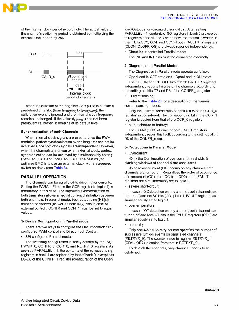
FUNCTIONAL DEVICE OPERATIONOPERATION AND OPERATING MODES
of the internal clock period accordingly. The actual value of the channel’s switching period is obtained by multiplying the internal clock period by 256.
When the duration of the negative CSB pulse is outside a predefined time slot (from t CSB(MIN) to t CSB(MAX)), the calibration event is ignored and the internal clock frequency remains unchanged. If the value (fPWM(0)) has not been previously calibrated, it remains at its default level.
Synchronization of both ChannelsWhen internal clock signals are used to drive the PWM
modules, perfect synchronization over a long time can not be achieved since both clock signals are independent. However, when the channels are driven by an external clock, perfect synchronization can be achieved by simultaneously setting PWM_en_1 = 1 and PWM_en_0 = 1. The best way to optimize EMC is to use an external clock with a staggered switch on delay (see Table 8).
PARALLEL OPERATIONThe channels can be paralleled to drive higher currents.
Setting the PARALLEL bit in the GCR register to logic [1] is mandatory in this case. The improved synchronization of both transistors allows an equal current distribution between both channels. In parallel mode, both output pins (HS[x]) must be connected (as well as both IN[x] pins in case of external control). CONF0 and CONF1 must be set to equal values.
1- Device Configuration in Parallel mode:There are two ways to configure the On/Off control: SPI-
configured PWM control and Direct Input Control.• SPI configured Parallel mode:
The switching configuration is solely defined by the (SI) PWMR_0, CONFR_0, OCR_0, and RETRY_0 registers. As soon as PARALLEL = 1, the contents of the corresponding registers in bank 1 are replaced by that of bank 0, except bits D6-D8 of the CONFR_1 register (configuration of the Open
load/Output short-circuited diagnostics). After setting PARALLEL = 1, contents of SO registers in bank 0 are copied to registers of bank 1 only when new information is written in them. Bits OD3, OD4, and OD5 of both FAULTR_s registers (OLON, OLOFF, OS) are always reported independently.• Direct Input controlled Parallel mode:
The IN0 and IN1 pins must be connected externally.
2- Diagnostics in Parallel Mode:The Diagnostics in Parallel mode operate as follows:
• OpenLoad in OFF state and - OpenLoad in ON state:The OL_ON and OL_OFF bits of both FAULTR registers
independently reports failures of the channels according to the settings of bits D7 and D6 of the CONFR_s register.• Current sensing:
Refer to the Table 23 for a description of the various current sensing modes.
Only the Current sense ratio of bank 0 (D5 of the OCR_0 register) is considered. The corresponding bit in the OCR_1 register is copied from that of the OCR_0 register.• output shorted to battery:
The OS-bit (OD3) of each of both FAULT registers independently report this fault, according to the settings of bit D8 of the CONFR_s reg.
3- Protections in Parallel Mode:• Overcurrent:
-Only the Configuration of overcurrent thresholds & blanking windows of channel 0 are considered.
-In case overcurrent (OC) occurs on any channel, both channels are turned-off. Regardless the order of occurrence of overcurrent (OC), both OC-bits (OD0) in the FAULT registers are simultaneously set to logic 1.• severe short-circuit:
In case of SC detection on any channel, both channels are turned-off and the SC bits (OD1) in both FAULT registers are simultaneously set to logic 1.• overtemperature:
In case of OT detection on any channel, both channels are turned-off and both OT bits in the FAULT registers (OD2) are simultaneously set to logic 1.• auto-retry:
Only one 4-bit auto-retry counter specifies the number of successive turn-on events on paralleled channels (RETRYR_0). The counter value in register RETRYR_1 (OD4…OD7) is copied from that in RETRYR_0.
To delatch the channels, only channel 0 needs to be delatched.
CSB
SICALR_s SI command
ignored
Internal clockperiod of channel s
tCSB
tCSB
Analog Integrated Circuit Device Data Freescale Semiconductor 33
06XS4200

FUNCTIONAL DEVICE OPERATIONOPERATION AND OPERATING MODES
PROTECTION AND DIAGNOSTIC FEATURES
PROTECTIVE FUNCTIONS
Overtemperature Fault (latchable fault)The channels have individual overtemperature detection.
As soon as a channel’s junction temperature rises above TSD (175 °C typ.), it is turned OFF, the overtemperature bit (OT = OD2) is set, and FSB = 0. FSB can only be reset by turning ON the channel when the junction temperature of both channels has dropped below the threshold: TJ < TSD. Overtemperature is detected in ON and in OFF state:• If the channel is ON, the associated output is switched
OFF, the OT bit is set, and FSB = 0. • If the channel is OFF: FSB goes to logic [0] and remain low
until the temperature of both channels is below TSD and any of the channels is turned on again.The auto-retry function (if activated) automatically turns on
the channel when the junction temperature has dropped below TSD. The OT fault bit can only be reset by reading out the FAULTR register, provided that TJ < TSD and FSB = 1 again.
Overcurrent Fault (latchable fault)When an overcurrent (OC) is detected, the channel is
immediately turned Off (after t FAULT seconds). The OC-bit is set to 1 and FSB becomes low [0]. Overcurrent is detected anytime the load current crosses an overcurrent threshold or exceeds the window width of the selected overcurrent protection profile. This profile is a stair function with windows the height and width of which are preselected through the SPI port. The maximum allowable value of the load current at a particular moment in time is defined by levels I_OCH and I_OCM and windows tOCM_x and tOCH (programmable by SPI bits). The steady-state overcurrent protection level I_OCL is defined by the settings of the OCL and HOCR bits. Anytime an overcurrent window is active, current sensing is blanked and SYNC becomes 1.
Overcurrent Duration CounterThe load current can spend only a defined amount of time
in a particular window of the overcurrent profile. If the time in the window exceeds the selected window width (tOCX) or the overcurrent threshold is crossed, the channel is turned off (OC fault), followed by auto-retry (if enabled). An internal overcurrent duration counter is employed for this function.
Overcurrent Detection on Resistive and Inductive LoadsAccording to the load type (resistive or inductive), one of
two different overcurrent profiles should be selected. This is done by connecting a resistor with the appropriate value between the CONF[0:1] pins and GND (Table 9).
When overcurrent windows are active, current sensing is disabled and the SYNCB pin remains high. This is illustrated by Figure 13. After turn on, the output voltage (second waveform (20 V/div.) and the output current (first waveform, 12 A/div.) rise immediately, but the current sense voltage (third waveform, 2.0 V/div, 1.0 V = 3.0 A) and its synchronization signal SYNC (fourth waveform, 5.0 V/div.) only become active at the end of the selected overcurrent window (duration tOCM2_L).
Figure 13. Current Sense Blanking during Overcurrent Window Activity
Activation of the lighting profile is time driven and activation of the DC motor profile is event driven, as explained below.
In lighting mode, the height of the overcurrent profile is defined by three different thresholds (I_OCH, I_OCM and I_OCL, which stand for the higher, the middle, and the lower overcurrent threshold), as illustrated by Figure 5. This profile has two adjacent windows the width of which is compatible with typical bulb inrush current profiles. The width of the first of these windows is either tOCH1 or tOCH2. The width of the second window is either tOCM1_L or tOCM2_L (see Table 18). The lighting profile is activated at each turn-on event, including auto-retry, except in switch mode. In switch mode, the profile is activated only at the first turn-on event, but is not
Table 9. Overcurrent Profile Selection
CONF[0:1] Resistor/Voltage Type of Load
1.0 kOhm < R(CONF[x]) < 10 kOhm
or 0 < V(CONF[X) < VIL (0.8 V)
resistive: CONF = 0,Lighting-Mode
R(CONF[x]) > 50 kOhmsor VIH (2.0 V)< V(CONF) < 5.0 V
inductive: CONF = 1,DC motor mode
Analog Integrated Circuit Device Data 34 Freescale Semiconductor
06XS4200
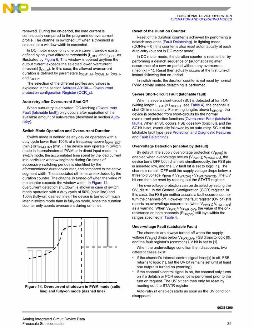
FUNCTIONAL DEVICE OPERATIONOPERATION AND OPERATING MODES
renewed. During the on-period, the load current is continuously compared to the programmed overcurrent profile. The channel is switched Off when a threshold is crossed or a window width is exceeded.
In DC motor mode, only one overcurrent window exists, defined by only two different thresholds (I_OCH and I_OCL) as illustrated by Figure 6. This window is opened anytime the output current exceeds the selected lower overcurrent threshold (IOCLx). In this case, the allowed overcurrent duration is defined by parameters tOCM1_M, tOCM2_M, tOCH1, and tOCH2.
The selection of the different profiles and values is explained in the section Address A0100 — Overcurrent protection configuration Register (OCR_s).
Auto-retry after Overcurrent Shut OffWhen auto-retry is activated, OC-latching (Overcurrent
Fault (latchable fault)) only occurs after expiration of the available amount of auto-retries (described in section Auto-retry).
Switch Mode Operation and Overcurrent DurationSwitch mode is defined as any device operation with a
duty cycle lower than 100% at a frequency above fPWM_EXT (min.) or fPWM_INT (min.). The device may operate in Switch mode in internal/external PWM or in direct input mode. In switch mode, the accumulated time spent by the load current in a particular window segment during On-times of successive switching periods is identified by the aforementioned duration counter, and compared to the active segment width. The associated off-times are excluded by the duration counter. The channel is turned-off when the value of the counter exceeds the window width. In Figure 14, overcurrent detection shutdown is shown in case of switch mode operation with a duty cycle of 50% (solid line) and 100% (fully-on, dashed line). The device is turned off much later in switch mode than in fully-on mode, since the duration counter only counts overcurrent during on-times.
Figure 14. Overcurrent shutdown in PWM mode (solid line) and fully-on mode (dashed line)
Reset of the Duration Counter Reset of the duration counter is achieved by performing a
delatch sequence (Fault Delatching). In lighting mode (CONFs = 0), this counter is also reset automatically at each auto-retry (but not in DC motor mode).
In DC motor mode, the duration counter is reset either by performing a delatch sequence or (automatically) after occurrence of a new on-period without any overcurrent ([hson[x] = 1). Reset then actually occurs at the first turn-off instant following that on-period.
In switch mode, the duration counter is not reset by normal PWM activity unless delatching is performed.
Severe Short-circuit Fault (latchable fault)When a severe short-circuit (SC) is detected at turn-ON
(wiring length LLOAD< LSHORT, see Table 4), the channel is shut Off immediately. For wiring lengths above LSHORT, the device is protected from short-circuits by the normal overcurrent protection functions (Overcurrent Fault (latchable fault)). When an SC occurs, FSB goes low (logic [0]), and the SC bit is set, eventually followed by an auto-retry. SC is of the latchable fault type (see Protection and Diagnostic Features and Fault Delatching).
Overvoltage Detection (enabled by default) By default, the supply overvoltage protection (VPWR) is
enabled when overvoltage occurs (VPWR > VPWR(OV)), the device turns OFF both channels simultaneously, the FSB pin is asserted low, and the OV fault bit is set to logic [1]. The channels remain OFF until the supply voltage drops below a threshold voltage VPWR < VPWR(OV) - VPWR(OVHYS). The OV bit can then be reset by reading out the STATR register.
The overvoltage protection can be disabled by setting the OV_dis = 1 in the General Configuration (GCR) register. In this case, the FSB pin neither asserts a fault occurrence, nor turn the channels off. However, the fault register (OV bit) still reports an overvoltage occurrence (when VPWR > VPWR(OV)) as a warning. When VPWR > VPWR(OV), the value of the on-resistance on both channels (RDS(on)) still lays within the ranges specified in Table 4.
Undervoltage Fault (Latchable Fault)The channels are always turned off when the supply
voltage (VPWR) drops below VPWR(UV). FSB drops to logic [0], and the fault register’s (common) UV bit is set to [1].
When the undervoltage condition then disappears, two different cases exist:• If the channel’s internal control signal hson[x] is off, FSB
returns to logic [1], but the UV bit remains set until at least one output is turned on (warning).
• If the channel’s control signal is on, the channel only turns on if a delatch or POR sequence is performed prior to the turn on request. The UV bit can then only be reset by reading out the STATR register.Auto-retry (if enabled) starts as soon as the UV condition
disappears.
Analog Integrated Circuit Device Data Freescale Semiconductor 35
06XS4200

FUNCTIONAL DEVICE OPERATIONOPERATION AND OPERATING MODES
Extended Mode ProtectionIn extended mode (6.0 V < VPWR < 8.0 V or 36 V < VPWR
< 58 V), the channels are still fault protected, but compliance with the specified protection levels is not guaranteed. The register settings however (including previously detected faults) remain unaltered, provided VDD is within the authorized range. Below 6.0 V, the channels are only protected from overtemperature, and this fault only reports in the SPI register the moment VPWR has again risen above VPWR(UV). To allow the outputs to remain ON between 36 and 58 V, overvoltage detection should be disabled (by setting OV_dis = 1 in the GCR register).
Faults (overtemperature, overcurrent, severe short-circuit, over and undervoltage) are reset if:• VDD < VDD(FAIL) with VPWR in the normal voltage range• VDD and VPWR are below the VSUPPLY(POR) voltage
threshold• The corresponding SPI register is read after the
disappearance of the failure cause (and delatching)
Drain/source Overvoltage protectionThe device tries to limit the Drain-to-Source voltage by
turning on the channel whenever VDS exceeds VDS(CLAMP). When a fault occurs (SC, OC, OT, UV), the device is rapidly switched Off (in t < tFAULT seconds), regardless the value of the selected slew rate. This may induce voltage surges on VPWR and/or the output pin (HS[x]) when connected to an inductive line/load. Turning on the device also dissipates the energy stored in the inductive supply line. This function monitors overvoltage for VPWR > 30 V. For supply voltages VPWR < 30 V, the device is protected from negative output voltages by automatically turning on the channel. The feature remains functional after device ground loss.
Supply Overvoltage ProtectionIn order to protect the device from excessive voltages on
the supply lines, the voltage between the device’s supply pins (VPWR and the GND) is monitored. When the VPWR-to-GND voltage exceeds the threshold VD_GND(CLAMP), the channel is automatically turned on. The feature is not operational in cases of ground loss.
Negative Output Voltage ProtectionThe device tries to limit the undervoltage on the output
pins HS[x] when turning off inductive loads. When the output voltage drops below VCL, the channel is switched on automatically. This feature is not guaranteed after a device ground loss.
The energy dissipation capabilities of the circuit are defined by the ECL [0:1] parameters. For inductive loads larger than 20 µH, it is recommended to employ a freewheeling diode. The three different overvoltage protection circuits are symbolically represented in Figure 15. The values of the clamping diodes are those specified in Table 4. Coupling factor k represents the current ratio between the current in
the supply voltage measurement diode (zener) and the current injected into the MOSFET’s gate to turn it on.
.
Figure 15. Supply and Output Voltage Protections
Reverse Voltage Protection on VPWR The device can withstand reverse supply voltages on
VPWR down to -28 V. Under these conditions, the outputs are automatically turned On and the channel’s On-resistance (RDS(on)) is similar to that during positive supply voltages. No additional components are required to protect the VPWR circuit except series resistors (>8.0 k) between the direct inputs IN[0:1] and VPWR in case they are connected to VPWR. The VDD pin needs reverse voltage protection from an externally connected diode (Figure 21).
Load and system Ground LossIn case of load ground loss, the channel’s state does not
change, but the device detects an OpenLoad fault. In case of a system GND loss, the channels are turned off.
Device Ground LossIn the (improbable) case the device loses all of its three
ground connections (pins 14, 17, and 22), the channels’ state (On/ Off), depends on several factors: the values of the series resistors connected to the device pins, the voltage of the direct input signals, the device’s momentary current consumption (influenced by the SPI settings) and the state of other high-side switches on the board when there are pins in common like FSB, FSOB and SYNC. In the below description, all voltages are referenced to the system (module) GND.
When series resistors are used, the channel state can be controlled by entering Fail-safe mode. The channels are turned off automatically when the voltage applied to the IN[x] input(s) through the series resistor(s) is not higher than VDD and be turned on when the IN[x] input(s) are tied to VPWR. Fail-Safe is entered under the following conditions:
• all unused pins are tied to the overall system’s GND connection by resistors > 8.0 k.
IMEG
GND
Load
HS[x]
DC
VDS(CLAMP)-Vth
VD_GND(Clamp)
I2
VCL-Vth
K.Iz
Vth
Analog Integrated Circuit Device Data 36 Freescale Semiconductor
06XS4200
FUNCTIONAL DEVICE OPERATIONOPERATION AND OPERATING MODES
• any device pin connected to external system components has a series resistors > 8.0 k (except pins VPWR, VDD, HS[0], HS[1] and R(CSNS)>2.0 k)
• pins FSB, FSOB and SYNC are in the logic high-state when they are shared with other devices. This means that none of the other devices is in Fault or Fail-safe mode, nor should current sensing be performed on any one of them when GND is lost
When no series resistors are employed, the channel state after GND loss is determined by the voltage on pins IN[0:1] and the voltage shift of the device GND. Device GND shift is determined by the lowest value of the external voltage applied to either pin of the following list: CLOCK, FSB, IN[0:1], FSOB, SCLK, CS,SI, SO, RSTB, CONF[0:1], SYNC, CSNS. When the device GND voltage becomes logic low (V(GND)< VIL), the SPI port continues to operate and the device operates normally. When the GND voltage becomes logic high (V(GND)> VIH), SPI communication is lost and Fail-safe mode is entered. When the voltage applied to the IN[0:1] input is VPWR, the channel is turned on when it is VDD, the channel is turned off if (VDD - V(GND)) < VIH.
SUPPLY VOLTAGES OUT OF RANGE
VDD Out of RangeIf the external VDD supply voltage is lost (or falls outside
the authorized range: VDD<VDD(FAIL)), the device enters Fail-safe mode, provided the VDD_FAIL_en bit had been set. Consequently, the contents of all SPI registers are reset. The channels are then controlled by the direct inputs IN[0 :1] (if VPWR is within the normal range). Since the VPWR pin supplies the circuitry of the SPI, current sense and most of the protective functions (overtemperature, overcurrent, severe short-circuit, short to VPWR, and OpenLoad detection circuitry), these faults are still detected and reported at the FSB pin. However, without VDD, the SO pin is no longer functional. The SPI registers can no longer be read and detailed fault information is unavailable. Current sensing also
becomes unavailable. If VDD_FAIL_EN wasn’t set before VDD was lost, the device remains SPI-controlled, even though the SPI registers can’t be read. No current flows from the VPWR to the VDD pin.
VPWR Supply Voltage Out of RangeIn case VPWR is below the undervoltage threshold
VPWR(UV), it is still possible to address the device by the SPI port, provided VDD is within the normal range. It does not prevent other devices from operating when a device is part of a daisy-chain. To accomplish this, RSTB must be kept at logic [1]. When the device operates at supply voltages above the maximum supply voltage (VPWR = 36 V), SPI communication is not affected (see Overvoltage Detection (enabled by default)). The internal pull-up and pull-down current sources on the SPI pins are not operational. Executing a Power-on-Reset (POR) sequence is recommended when VPWR re-enters its authorized range. No current flows from the VDD to the VPWR pin.
Loss of VPWR, Loss of VDD and Power-on-Reset (POR)In typical applications (Figure 21 and Figure 22), an
external voltage regulator may be used to derive VDD from VPWR. In wake mode, a Power-on-Reset (POR) sequence executes and the POR bit (OD6 of the STATR register) is set if:
1. VPWR > VPWR (POR), after a period VPWR < VPWR (POR) (and VDD < VDD (POR) before and after)
2. VDD > VDD (POR) after a period with VDD < VDD (POR) (VPWR < VPWR (POR) before and after)
POR is also set at the transition to wake-up (by setting RSTB = 1 or IN[x] = 1) when VPWR > VPWR (POR) (before and after) or VDD >VDD(POR) (before and after). POR is not performed when VPWR > VPWR (POR) after a period VPWR < VPWR (POR) (and VDD > VDD (POR) permanently).
Analog Integrated Circuit Device Data Freescale Semiconductor 37
06XS4200

FUNCTIONAL DEVICE OPERATIONOPERATION AND OPERATING MODES
Figure 16. State Machine: Fault Occurrence and Auto-retry
AUTO-RETRYThe auto-retry circuitry automatically tries to turn on the
channel on a cyclic basis. Only faults of the latchable type (overcurrent, severe short-circuit, overtemperature (OT), and undervoltage (UV)) may activate auto-retry. For UV and OT faults, auto-retry only starts after disappearance of the failure cause (when auto-retry is enabled). The retry condition is expressed by:
Retry[x] = OC[x] or SC[x] or OT[x] or UV.If Auto-retry has been enabled, its mode of operation
depends on the settings of the auto-retry related bits (bits D0...D3 of the SI-RETRY_s register, see Table 12) and the available amount of auto-retries (bits OD7...OD4 of the SO-RETRY_s reg.). More details can be found in Amount Of Auto-retries.
If Auto-retry is disabled, latchable faults immediately latches upon their occurrence (see Protection and Diagnostic Features).
Auto-retry ConfigurationTo enable the auto-retry function, bit retry_s (D0 of the SI
RETRY_s register) has to be set to the appropriate value. Auto-retry is enabled for retry_s = 0 when the channel is configured for lighting applications (CONF = 0). It is enabled for retry_s = 1 for DC motor applications (CONF[x] = 1).
If auto-retry is enabled, an auto-retry sequence starts when the channel’s fault control signal is set to 1 (fc[x] = 1, see Fault Delatching) and the retry condition applies (Retry[x] = 1, see Auto-retry).
When a failure occurs (fault = 1), the channel automatically switches on again after the auto-retry period. The value of this period (tAUTO) is set through the SPI port (bits D2 and D3 of the RETRY_s register, see Table 22). When the failure cause disappears before expiration of the available amount of auto-retries, the device behaves normally (FSB = 1), but the retry counter keeps its current value and the fault bit remains set until it is cleared. This guarantees a maximum device availability without preventing fault detection.
OFF ON LatchedOFF
OFF ON(OV = 1)
(fc[x] = 1 and (OV = 0))
(fc[x]= 0 or OV = 1)
(fc[x] = 0)
(fc[x] = 0)
(fc[x] = 0)
(Retry = 1)= > count = count+1
(Retry = 1)(count = 16)
(after Retry Period and OV = 0 and OT = 0 and UV = 0)
(OpenLoadOFF = 1 or OS = 1
(OpenLoadOFF = 1 or OS = 1
(OpenloadOFF = 1 or OS = 1
(OpenLoadON = 1)
(OpenLoadON = 1)
or OV = 1)
or OV = 1
or OV = 1)
or UV = 1or OT = 1)
Auto-retry Loop
Table 10. Auto-Retry Activation for Lamps (CONF = 0) and DC Motors (CONF = 1)
CONF[x] Retry_s bit auto-retry
0 0 enabled
0 1 disabled
1 0 disabled
1 1 enabled
Analog Integrated Circuit Device Data 38 Freescale Semiconductor
06XS4200
FUNCTIONAL DEVICE OPERATIONOPERATION AND OPERATING MODES
Amount Of Auto-retriesIn case the device is configured for an unlimited amount of
auto-retries (Retry_unlimited_s = 1), auto-retry continues as long as the device remains powered. The channel never be latches off.
In case a limited amount of retries is selected (Retry-unlimited_s = 0), auto-retry continues as long as the value of the 4-bit auto-retry counter does not exceed 15 (bits OD4...OD7 of the RETRY_s register). After 15 retries, the Rfull bit of the STATR (OD4 for channel 0, OD5 for channel 1) register is set to logic high. The amount of available auto-retries is then reduced to one. If the fault still hasn’t disappeared at the next retry, the corresponding channel switches off definitively and the fault is latched (FSB = 0, see Protection and Diagnostic Features and Fault Delatching).
Any channel can be turned on at any moment during the auto-retry cycle by performing a delatch sequence. However, this does not reset the retry counter.
The value of the auto-retry counter can be read back in Normal mode only (SO-RETRYR register bits OD7-OD4).
Reset of the Auto-retry CounterAny one of the below events reset the retry counter:
• Fail-safe is entered (Fail-safe Mode)• Sleep mode is left (Sleep Mode)• POR occurs (Supply Voltages Out of Range)• the retry function is set to unlimited (bit Retry-
unlimited_s = 1 (D1 = 1))• the retry function is disabled (retry_s bit = D0 of the
RETRY_s register under goes a 1-0 transition for CONF = 1 and a 0-1 transition for CONF = 0).If the channel is latched at the moment the auto-retry
counter was reset (case 4), the channel is delatched, and be turned on after one retry period (if retry was enabled).
Auto-retry and Overcurrent DurationDuring the on-period following an auto-retry, the load
current profile is compared to the length and height of the selected overcurrent threshold profile, as described in the section on overcurrent protection (See Overcurrent Fault (latchable fault)).
When the lighting profile is activated, the overcurrent duration counter is reset at each auto-retry (to allow sustaining new inrush currents).
For DC motor mode however, it is only reset at the turn-off event of the first PWM period without any overcurrent (see Reset of the Duration Counter). Figure 16 gives a description of the retry state machine with the various transitions between operating modes.
DIAGNOSTIC FEATURESDiagnostic functions OpenLoad-in-On state (OLON),
OpenLoad-in-Off-state (OLOFF) and output short-circuited to VPWR (OS) are operational over the frequency and duty cycle ranges specified in Table 5.
Occurrence of an OLON, OLOFF, or OS fault sets the associated bit in the FAULTR_s register but does not trigger automatic turn-off. Any of these diagnostic functions can be disabled by setting OLON_dis_s = 1, OLOFF_dis_s = 1, or OS_dis_s = 1 (bits D8...D6 of the CONFR reg.).
The functions are guaranteed over the specified ranges for output capacitor values up to 22 nF (+/-20%).
Output shorted-to-VPWR FaultThe device detects short-circuits between the output and
VPWR. The detection is performed during the Off-state. The output-shorted-to-VPWR fault-bit (OS_s) is set whenever the output voltage rises above VOSD(THRES). The fault is reported in real time on the FSB pin and saved by the OS_s bit. Occurrence of this fault does not trigger automatic turn-off.
Even if the short-circuit disappears, the OS_s bit does not clear until the FAULTR register is read. The function may be disabled by setting OS_dis_s = 1. The function operates over the duty cycle ranges specified in Diagnostic Features.
This type of event shall be limited to 1000 min during the vehicle lifetime. In case of permanent output shorted to the battery condition, it is needed to turn-on the corresponding channel.
OpenLoad Detection In Off StateOpenLoad-in-OFF-state detection (OL_OFF) is performed
continuously during each OFF-state (both for CSR0 and CSR1). This function is implemented by injecting a small current into the load (IOLD(OFF)). When the load is disconnected, the output voltage rises above VOLD(THRES). OL_OFF is then detected and the OL_OFF bit in the FAULTR register is set. If disappearance of the open load fault is detected, the FSB output pin returns to a high immediately, but the OL_OFF bit in the fault register remains set until it is cleared by a read out of the FAULTR register. The function may be disabled by setting OLOFF_dis_s = 1. The function operates over the duty cycle ranges specified in section Diagnostic Features.
OpenLoad Detection In On State (OL_ON)OpenLoad-in-ON state detection (OLON) is performed
continuously during the On-state for CSR0 over the ranges specified in section Diagnostic Features. An OpenLoad in On state fault is detected when the load current is lower than the OpenLoad current threshold IOLD(ON). This happens at IOLD(ON) = 500 mA (typ.) for high current sense mode (CSR0), and at 7.0 mA (typ.) for low current mode. FSB is asserted low and the OLON bit in the fault register is set to 1 but the channel remains On. FSB goes high as soon as disappearance of the failure cause is detected, but the OL_ON bit remains set.
In high current mode (CSR0), OpenLoad in On state detection is done continuously during the On-state and the OLON-bit remains set even if the fault disappears.
In high current mode, the OLON-bit is cleared when the FAULTR register is read during the Off state, even if the fault
Analog Integrated Circuit Device Data Freescale Semiconductor 39
06XS4200
FUNCTIONAL DEVICE OPERATIONOPERATION AND OPERATING MODES
hasn't disappeared. The OLON bit is also cleared when the FAULTR register is read during the ON state, provided the failure cause (load disconnected) has disappeared.
In low current mode (CSR1), OL_ON is done periodically instead of continuously and only operates when fast slew rate is selected. When the internal PWM module is used with an internal or external clock (case 1), the period is 150 ms (typ.). When the direct inputs are used (case 2), the period is that of the input signal. The detection instants in both cases are given by the following:
1. In internal PWM (int./ext. clock), low current mode (CSR1), OpenLoad-in-ON state detection is not performed each switching period, but at a fixed frequency of about 7.0 Hz (each tOLLED = 150 ms typ.). The function is available for a duty cycle of 100%. OLON detection is also performed at 7.0 Hz, at the first turn-off event occurring 150 ms after the previous OL_ON detection event (before OS and OL_OFF).
2. In direct input, low current mode (CSR1), OL_ON is performed each switching period (at the turn-off instant) but the duty cycle is restricted to the values. Consequently, when the signal on the IN[x] pin has a duty cycle of 100%, OL_ON is not performed. To solve this problem, either the internal PWM function must be activated with a duty cycle of 100%, or the channel’s direct input must be disabled by setting Dir_dis_s = 1 (bit D5 of the CONFR-s register). The OLON-bit is only reset when the FAULTR register is read after occurrence of an OL_ON-detection event without fault presence.
OpenLoad Detection in Discontinuous Conduction ModeIf small inductive loads (solenoids / DC motors) are driven
at low frequencies, discontinuous conduction mode may occur. Undesired OpenLoad in On state errors may then be detected, as the inductor current needs some time to rise above the OpenLoad detection threshold after turn-on. This problem can be solved by increasing the switching frequency or by disabling the function and activating OpenLoad in Off state detection instead.
When small DC motors are driven in discontinuous conduction mode, undesired OpenLoad in Off state detection may also occur when the load current reaches 0 A during the Off state. This problem can be solved by increasing the switching frequency or by enabling OpenLoad in Off state detection only during a limited time, preferably directly after turn-off (see Diagnostic Features). The signal on the SYNC pin can be used to identify the turn-off instant.
CURRENT & TEMPERATURE SENSINGThe scaled values of either of the output currents or the
temperature of the device’s GND pin (#14) can be made available at the CSNS pin. To monitor the current of a particular channel or the general device temperature, the CSNS0_en and CSNS1_en bits in the General Configuration Register (GCR) must be set to the appropriate values. When
overcurrent windows are active, current sensing is disabled and the SYNCB pin remains high.
Instantaneous and Sampled Current SensingThe device offers two possibilities for load current sensing:
instantaneous (synchronous) sensing mode and track & hold mode (see Figure 9). In synchronous mode, the load current is mirrored through the current sense pin (Output Current Monitoring (CSNS)) and is therefore synchronous with it. After turn-off, the current sense pin does not output the channel current. In track & hold mode however, the current sense pin continues to mirror the load current as it was just before turn-off. Synchronous mode is activated by setting the T_H_en bit to 0, and Track & Hold mode by setting the T_H_en bit to 1.
Current Sense Ratio SelectionThe load current is mirrored through the CSNS pin with a
sense ratio (Figure 17) selected by the CSNS_ratio bit in the OCR register. To achieve optimal accuracy at low current levels, the lower current sensing ratio, called CSR1, must be selected. In that case, the overcurrent threshold levels are decreased. The best accuracy that can be obtained for either ratio is shown in Figure 18. The amount of current the CSNS pin can sink is limited to ICSNS,MAX..The CSNS pin must be connected to a pull-down resistor (470 Ohm < R(CSNS) <10 kOhm, 1.0 kOhm typical), in order to generate a voltage output. A small low-pass filter can be used for filtering out switching transients (Figure 21). Current sensing operates for load currents up to the lower overcurrent threshold (OCLx A).
Synchronous Current Sensing ModeFor activation of synchronous mode, T_H_en must be set
to 0 (default). After turn-on, the CSNS output current accurately reflects the value of the channel’s load current after the required settling time. From this moment on (CSNS valid), the SYNC pin goes low and remain low until a switch off signal (internal/external) is received. This allows synchronization of the device’s current sensing feature with an external process running on a separate device (see Current Sense Synchronization (SYNC)). After turn-off, the load current does not flow through the switch, and the load current cannot be monitored.
Track & Hold Current Sensing ModeIn Track & Hold mode (T&H) (T_H_en = 1), conversely
from synchronous mode, the CSNS output current is available even after having switched off the load. This feature is useful when the device operates autonomously (internal clock/PWM), since it allows current monitoring without any synchronization of the device. An external sample and hold (S/H) capacitor is not required. After turn on, the CSNS output current reflects the channel’s load current with the specified accuracy after occurrence of the negative edge on the SYNC pin, as in synchronous mode (see Current Sense Synchronization (SYNC)). However, at the switch-off instant,
Analog Integrated Circuit Device Data 40 Freescale Semiconductor
06XS4200
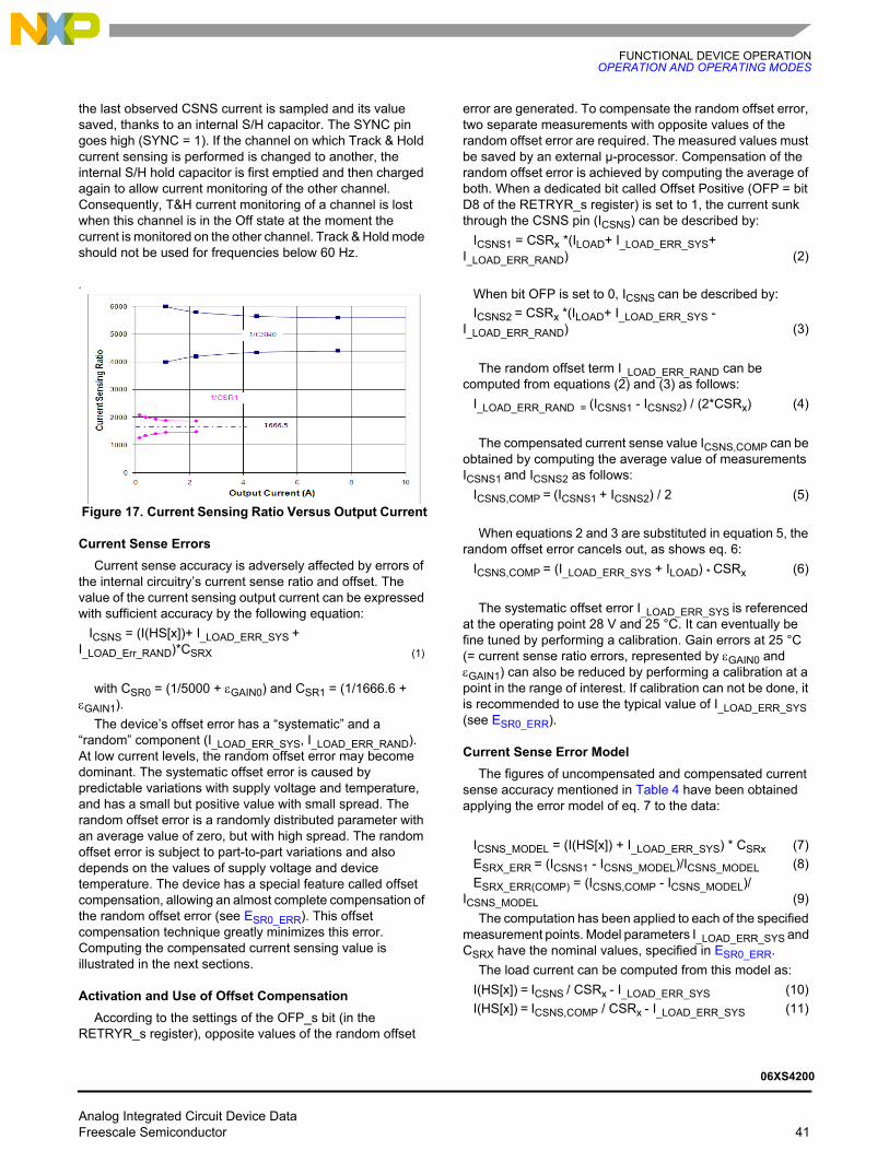
FUNCTIONAL DEVICE OPERATIONOPERATION AND OPERATING MODES
the last observed CSNS current is sampled and its value saved, thanks to an internal S/H capacitor. The SYNC pin goes high (SYNC = 1). If the channel on which Track & Hold current sensing is performed is changed to another, the internal S/H hold capacitor is first emptied and then charged again to allow current monitoring of the other channel. Consequently, T&H current monitoring of a channel is lost when this channel is in the Off state at the moment the current is monitored on the other channel. Track & Hold mode should not be used for frequencies below 60 Hz.
.
Figure 17. Current Sensing Ratio Versus Output Current
Current Sense ErrorsCurrent sense accuracy is adversely affected by errors of
the internal circuitry’s current sense ratio and offset. The value of the current sensing output current can be expressed with sufficient accuracy by the following equation:
ICSNS = (I(HS[x])+ I_LOAD_ERR_SYS + I_LOAD_Err_RAND)*CSRX (1)
with CSR0 = (1/5000 + εGAIN0) and CSR1 = (1/1666.6 + εGAIN1).
The device’s offset error has a “systematic” and a “random” component (I_LOAD_ERR_SYS, I_LOAD_ERR_RAND). At low current levels, the random offset error may become dominant. The systematic offset error is caused by predictable variations with supply voltage and temperature, and has a small but positive value with small spread. The random offset error is a randomly distributed parameter with an average value of zero, but with high spread. The random offset error is subject to part-to-part variations and also depends on the values of supply voltage and device temperature. The device has a special feature called offset compensation, allowing an almost complete compensation of the random offset error (see ESR0_ERR). This offset compensation technique greatly minimizes this error. Computing the compensated current sensing value is illustrated in the next sections.
Activation and Use of Offset CompensationAccording to the settings of the OFP_s bit (in the
RETRYR_s register), opposite values of the random offset
error are generated. To compensate the random offset error, two separate measurements with opposite values of the random offset error are required. The measured values must be saved by an external µ-processor. Compensation of the random offset error is achieved by computing the average of both. When a dedicated bit called Offset Positive (OFP = bit D8 of the RETRYR_s register) is set to 1, the current sunk through the CSNS pin (ICSNS) can be described by:
ICSNS1 = CSRx *(ILOAD+ I_LOAD_ERR_SYS+ I_LOAD_ERR_RAND) (2)
When bit OFP is set to 0, ICSNS can be described by:ICSNS2 = CSRx *(ILOAD+ I_LOAD_ERR_SYS -
I_LOAD_ERR_RAND) (3)
The random offset term I_LOAD_ERR_RAND can be computed from equations (2) and (3) as follows:
I_LOAD_ERR_RAND = (ICSNS1 - ICSNS2) / (2*CSRx) (4)
The compensated current sense value ICSNS,COMP can be obtained by computing the average value of measurements ICSNS1 and ICSNS2 as follows:
ICSNS,COMP = (ICSNS1 + ICSNS2) / 2 (5)
When equations 2 and 3 are substituted in equation 5, the random offset error cancels out, as shows eq. 6:
ICSNS,COMP = (I_LOAD_ERR_SYS + ILOAD) * CSRx (6)
The systematic offset error I_LOAD_ERR_SYS is referenced at the operating point 28 V and 25 °C. It can eventually be fine tuned by performing a calibration. Gain errors at 25 °C (= current sense ratio errors, represented by εGAIN0 and εGAIN1) can also be reduced by performing a calibration at a point in the range of interest. If calibration can not be done, it is recommended to use the typical value of I_LOAD_ERR_SYS (see ESR0_ERR).
Current Sense Error ModelThe figures of uncompensated and compensated current
sense accuracy mentioned in Table 4 have been obtained applying the error model of eq. 7 to the data:
ICSNS_MODEL = (I(HS[x]) + I_LOAD_ERR_SYS) * CSRx (7)ESRX_ERR = (ICSNS1 - ICSNS_MODEL)/ICSNS_MODEL (8)ESRX_ERR(COMP) = (ICSNS,COMP - ICSNS_MODEL)/
ICSNS_MODEL (9)The computation has been applied to each of the specified
measurement points. Model parameters I_LOAD_ERR_SYS and CSRX have the nominal values, specified in ESR0_ERR.
The load current can be computed from this model as:I(HS[x]) = ICSNS / CSRx - I_LOAD_ERR_SYS (10)I(HS[x]) = ICSNS,COMP / CSRx - I_LOAD_ERR_SYS (11)
Analog Integrated Circuit Device Data Freescale Semiconductor 41
06XS4200

FUNCTIONAL DEVICE OPERATIONLOGIC COMMANDS AND SPI REGISTERS
Using expression (11) generally gives more accurate values than expression (10), since in expression (11), random offset errors have been compensated.
Offset Compensation in Track & Hold ModeIn Track & Hold mode, the last observed sense current
(ICSNS) is sampled at the switch off instant. This takes into account the currently active settings of the OFP_s offset compensation bit. Changing the value of the OFP bit during the switch’s off time produces an identical value of the current sense output. Consequently, to implement the before mentioned offset compensation technique, the channel must have been turned on at least once prior to sensing the output current with an opposite value of the OFP bit.
System Requirements for Current MonitoringCurrent monitoring is usually implemented by reading the
(RC-filtered) voltage across the pull-down resistor connected between the CSNS pin and GND (Figure 21). Therefore, measurements (1) and (2) must be spaced sufficiently wide apart (e.g. 5 time constants) to get stabilized values, but close enough to be sure that the offset value wasn’t changed. The A/D converter of the external micro controller that is used to read the current sense voltage V(csns) must have sufficient resolution to avoid introducing additional errors.
Accuracy with and without Offset CompensationThe sensing accuracy for CSR0 and CSR1, obtained
before and after offset compensation, is shown in Figure 18.
.
Figure 18. Current Sense Accuracy versus Output Current
In Track & Hold mode, the accuracy of the current sense function is lowered according to the values shown in Figure 19 (error percentage as a function of the switch-off
time is displayed, for CSR0 and CSR1). Track & Hold mode should not be used below f = 60 Hz.
Figure 19. Track and Hold Current Sense Accuracy
Temperature Prewarning DetectionIn Normal mode, the temperature prewarning (OTW) bit is
set (bit OD8 of the FAULTR register) when the observed temperature of the GND pin is higher than TOTWAR (pin #14, see Figure 3). The feature is useful when the temperature of the direct surroundings of the device must be monitored. To be able to reset the OTW-bit, the FAULTR register must be read after the moment that temperature T °C < TOTWAR.
Switching State MonitoringThe switching state (On/Off) of the channels is reported in
real time by bits OUT[x] in the STATR register (bit OD0/OD1). The Out[x] bit is asserted logic high when the channel is on (output voltage V(HS[x]) higher than VPWR /2). When supply voltage VPWR drops below 13 V, the reported switching state may not correspond to the state of the channel’s control signal hson[x] in case of an open load fault (see Factors Determining the Channel’s Switching State).
EMC PERFORMANCESSpecified EMC performance is board and module
dependent and applies to a typical application (Figure 21). The device withstands transients per ISO 7637-2 /24 V. An external freewheeling diode connected to at least one output is required for sustaining ISO 7637-2 Pulse 1 (-600 V). To withstand Pulse 2, at least one of the two channels must be connected to a typical load (bulb). It withstands electric fields up to 200 V/m and Bulk Current Injection (BCI) up to 200 mA per ISO11452.
LOGIC COMMANDS AND SPI REGISTERS
SPI PROTOCOL DESCRIPTIONThe SPI interface offers full duplex, synchronous data
transfer over four I/O lines: Serial Input (SI), Serial Output (SO), Serial Clock (SCLK), and Chip Select (CSB).The SI / SO pins of the device follow a first-in first-out (D15 to D0)
protocol. Transfer of input and output words starts with the most significant bit (MSB). All inputs are compatible with 5.0 V or 3.3 V CMOS logic levels. Parity check is performed after transfer of each 16-bit SPI data word.The SPI interface can be driven without series resistors provided that voltage
Analog Integrated Circuit Device Data 42 Freescale Semiconductor
06XS4200

FUNCTIONAL DEVICE OPERATIONLOGIC COMMANDS AND SPI REGISTERS
ratings on VDD and SPI pins (Table 3) aren’t exceeded. Unused SPI-pins must be tied to GND, eventually by resistors (see Device Ground Loss).
Figure 20. 16-Bit SPI Interface Timing Diagram
SERIAL INPUT COMMUNICATION PROTOCOLSPI communication requires that RSTB = high. SPI
communication is accomplished with 16-bit messages. A valid message must start with the MSB (D15) and end with the LSB (D0) (Table 11). Incoming messages are interpreted according to Table 12. The MSB, D15, is the watchdog bit (WDIN). Bit D14, Parity check (P), must be set such that the total number of 1-bits in the SPI word is even (P = 0 for an even number of 1-bits and P = 1 for an odd number). Bank selection is done by setting bit D13. Bits D12: D10 are used for register addressing. The remaining ten bits, D9 : D0, are used to configure the device and activate diagnostic and protective functions. Multiple messages can be transmitted for applications with daisy chaining (or to validate already transmitted data) by keeping the CSB pin at logic 0. Messages with a length different from a multiple of 16 or with a parity error is ignored. The device has thirteen input registers for device configuration and thirteen output registers containing the fault/device status and settings. Table 12 gives the SI register function assignment. Bit names with extension “_s” refer to functions that have been implemented independently for each of both channels.
SERIAL PORT OPERATIONWhen Chip Select occurs (1-to-0 transition on the CSB
pin), the output register data is clocked out of the SO pin
(MSB-first) at the serial clock frequency (SLCK). Bits at the SI pin are clocked in at the same time. The first sixteen SO register bits are those addressed by the previous SI word (bit D13, D2…D0 of the STATR_s input register). At the end of the chip select event (0-to-1 transition), the SI register contents are latched. The second SPI word clocked out of the Serial Output (SO) after the first CSB event represents the initial SO register contents. This allows daisy chaining and data integrity verification.
The message length is validated at the end of the CSB event (0-to-1 transition). If it is valid (multiples of 16, no parity error), the data is latched into the selected register. After latch-in, the SO pin is tri-stated and the status register is updated with the latest fault status information.
Daisy Chain OperationDaisy-chaining propagates commands through devices
connected in series. The commands enter the device at the SI pin and leave it by the SO pin, delayed by one command cycle of 16 bits. To address a particular device in a daisy chain, the CSB pin of all the devices in that chain has to be kept low until the SPI message has arrived at its destination. Once the command has been clocked in by the addressed device, it can be executed by setting CSB = 1.
1. RST must be in a logic [1] state during data transfer.2. Data enter the SI pin starting with D15 (MSB) and ending with bit D0.3. Data are available on the SO pin starting with bit 0D15 (MSB) and ending with bit 0(OD0).
Notes 1. RSTB must be in a logic [1] state during data transfer.2. Data enter the SI pin starting with D15 (MSB) and ending with bit D0.3. Data are available on the SO pin starting with bit 0D15 (MSB) and ending with bit 0(OD0).
Notes
CSB
SCLK
SI
SO
D15 D14 D13 D12 D11 D10 D9 D8 D7 D6 D5 D4 D3 D2 D1 D0
OD15 OD14 OD13 OD12 OD11 OD10 OD9 OD8 OD7 OD6 OD5 OD4 OD3 OD2 OD1 OD0
Analog Integrated Circuit Device Data Freescale Semiconductor 43
06XS4200
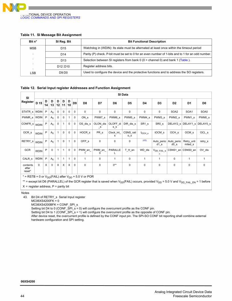
FUNCTIONAL DEVICE OPERATIONLOGIC COMMANDS AND SPI REGISTERS
Table 11. SI Message Bit Assignment
Bit n° SI Reg. Bit Bit Functional Description
MSB....
LSB
D15 Watchdog in (WDIN): Its state must be alternated at least once within the timeout period
D14 Parity (P) check. P-bit must be set to 0 for an even number of 1-bits and to 1 for an odd number.
D13 Selection between SI registers from bank 0 (0 = channel 0) and bank 1 (Table ).
D12 : D10 Register address bits.
D9:D0 Used to configure the device and the protective functions and to address the SO registers.
Table 12. Serial Input register Addresses and Function Assignment
SI Register
SI Data
D 15 D 14
D 13
D 12
D 11
D 10 D9 D8 D7 D6 D5 D4 D3 D2 D1 D0
STATR_s WDIN P A0 0 0 0 0 0 0 0 0 0 0 SOA2 SOA1 SOA0
PWMR_s WDIN P A0 0 0 1 0 ON_s PWM7_s PWM6_s PWM5_s PWM4_s PWM3_s PWM2_s PWM1_s PWM0_s
CONFR_s WDIN P A0 0 1 0 0 OS_dis_s OLON_dis_s
OLOFF_dis_s
DIR_dis_s SR1_s SR0_s DELAY2_s DELAY1_s DELAY0_s
OCR_s WDIN P A0 1 0 0 0 HOCR_s PR_s Clock_int_s
CSNS_ratio_s
tOCH_s tOCM_s OCH_s OCM_s OCL_s
RETRY_s WDIN P A0 1 0 1 0 OFP_s 0 0 0 (43) Auto_period1_s
Auto_period0_s
Retry_unlimited_s
retry_s
GCR WDIN P 0 1 1 0 0 PWM_en_1
PWM_en_0
PARALLEL
T_H_en WD_dis VDD_FAIL_en
CSNS1_en CSNS0_en OV_dis
CALR_s WDIN P A0 1 1 1 0 1 0 1 0 1 1 0 1 1
contents after
reset*
0 X 0 X X X 0 0 0 0** 0 0 0 0 0 0
* = RSTB = 0 or VDD(FAIL) after VDD = 5.0 V or POR** = except bit D6 (PARALLEL) of the GCR register that is saved when VDD(FAIL) occurs, provided VDD = 5.0 V and VDD_FAIL_EN = 1 beforeX = register address, P = parity bit
Notes43. Bit D4 of RETRY_s Serial Input register
MC06XS4200FK = 0 MC06XS4200BFK = CONF_SPI_s Setting bit D4 to 0 (CONF_SPI_s = 0) will configure the overcurrent profile as the CONF pin. Setting bit D4 to 1 (CONF_SPI_s = 1) will configure the overcurrent profile as the opposite of CONF pin. After device reset, the overcurrent profile is defined by the CONF input pin. The SPI-SO CONF bit reporting shall combine external hardware configuration and SPI setting.
Analog Integrated Circuit Device Data 44 Freescale Semiconductor
06XS4200

FUNCTIONAL DEVICE OPERATIONLOGIC COMMANDS AND SPI REGISTERS
SI REGISTER ADDRESSINGThe address in the title of the following sections (A0xxx)
refer to bits D[13:10] of the SPI word required to address the associated SI register. Bit A0 = D13 selects between registers of bank 0 and bank 1 (Table 14). The function assignment of register bits D[8:0] is described in the associated section. The “_s” behind a register name indicates that the variable applies to the register contents of both banks. ADDRESS A0000 — STATUS REGISTER (STATR_S)
To read back the contents of any of the 13 SO registers, bits D[13:10] of the channel’s SI STATR register must be set to A0000 and bits D[2:0] in the same SPI word to the address of the desired SO register. The SO registers thus addressed are: STATR, FAULTR_s, PWMR_s, CONFR_s, OCR_s, RETRY_s, GCR, and DIAGR (Table 13).
Table 13. Serial Output Register Bit Assignment
bits D13, D2, D1, D0
of the Previous STATR
SO Returned Data
SOA3
SOA2
SOA1
SOA0
OD15
OD14
OD13
OD12
OD11
OD10
OD9 OD8 OD7 OD6 OD5 OD4 OD3 OD2 OD1 OD0
STATR 0 0 0 0 WDIN PF SOA
3SOA
2SOA1
SOA0
NM OV UV POR R_FUL
L1R_FUL
L0 FAULT1 FAULT0 OUT1 OUT0
FAULTR_s A0 0 0 1 WDI
N PF SOA3
SOA2
SOA1
SOA0
NM OTW 0 0 OLON
_sOLOFF
_s OS_s OT_s SC_s OC_s
PWMR_s A0 0 1 0 WDI
N PF SOA3
SOA2
SOA1
SOA0
NM
ON_s
PWM7_s
PWM6_s
PWM5_s
PWM4_s
PWM3_s PWM2_s PWM1_s PWM0_s
CONFR_s A0 0 1 1 WDI
N PF SOA3
SOA2
SOA1
SOA0
NM
OS_dis_s
OLON_dis_s
OLOFF_dis_s
DIR_dis_s
SR1_s SR0_s DELAY2_s DELAY1_s
DELAY0_s
OCR_s A0 1 0 0 WDIN PF SOA
3SOA
2SOA1
SOA0
NM
HOCR_s PR_s Clock_i
nt_sCSNS_ratio_s
tOCH_s
tOCM_s OCH_s OCM_s OCL_s
RETRYR_s A0 1 0 1 WDI
N PF SOA3
SOA2
SOA1
SOA0
NM
OFP R3 R2 R1 R0 Auto_period1_s
Auto_period0_s
Retry_unlimited_s
retry_s
GCR 0 1 1 0 WDIN PF SOA
3SOA
2SOA1
SOA0
NM
PWM_en_
1
PWM_en_
0
PARALLLEL
T_H_en
WD_dis
VDD_Fail_en
CSNS1_en CSNS0_en
OV_dis
DIAGR 0 1 1 1 WDIN PF SOA
3SOA
2SOA1
SOA0
NM
CONF1
CONF0 ID1 ID0 IN1 IN0 CLOCK_fail CAL_fail1 CAL_fail0
contents after
reset or failure*
N/A
N/A
N/A
N/A 0 0 0 0 0 0 0 0 0 0** 0*** 0
0 00 0
* = RSTB = 0 or VDD(FAIL) after VDD = 5.0 V, or POR** = except bit D6 (PARALLEL) of the GCR register that is saved when VDD(FAIL) occurs provided VDD = 5.0 V and VDD_Fail_en = 1 before*** = except bit D7 (POR) of the STATR register that is saved when VDD(FAIL) occurs after VDD = 5.0 V and VDD_Fail_en = 1 (fail-safe mode)x = register address, PF = parity Fault
Table 14. Value of bit A0 Required for Addressing Register Banks 0 or 1
Value A0 (D13) Bank
0 0 = channel 0 (default)
1 1 = channel 1
Analog Integrated Circuit Device Data Freescale Semiconductor 45
06XS4200

FUNCTIONAL DEVICE OPERATIONLOGIC COMMANDS AND SPI REGISTERS
ADDRESS A0001— PWM CONTROL REGISTER (PWMR_S)
The PWMR_s register contents determines the value of the PWM duty cycle at the output (Table 12), both for internal and external clock signals.
Bit D8 must be set to 1 to activate this function. The desired value of duty cycle is obtained by setting Bits D7:D0 to one of the 256 levels as shown in Table 7.To start the PWM function at a known point in time, the PWM_en_s bit (both in the GCR register) must be set to 1.
ADDRESS A0010— CHANNEL CONFIGURATION REGISTER (CONFR_S)
The CONFR_s is used to select the appropriate value of slew rate and turn-ON delay. The settings of Bits D[8:6] determine the activation of OpenLoad and short-circuit (to VPWR) detection. Bit D13 ( = A0) of the incoming SPI word determines which of both CONFR registers is addressed (Table 14).
Setting bit D8 (OS_dis_s) to logic [1] disables detection of short-circuits between the channel’s output pin and the VPWR pin. The default value [0] enables the feature.
Setting bit D7 (OLON_dis_s) to logic [1] disables detection of OpenLoad in the On state for the selected channel. The default value [0] enables this feature (Table 15).
Setting bit D6 (OLOFF_dis_s) to logic [1] disables detection of OpenLoad in the OFF state. The default value [0] enables the feature, see Table 15.
Setting bit D5 (DIR_DIS_s) to logic [0] enables direct control of the selected channel. Setting bit D5 to logic [1] disables direct control. In that case, the channel state is determined by the settings of the internal PWM functions.
D4:D3 bits (SR1_s and SR0_s) control the slew rate at turn on and turn off (Table 16). The default value ([00]) corresponds to the medium slew rate. Rising and falling edge slew rates are identical.
Delaying a channel’s turn-On instant with respect to the other is accomplished by setting bits D2 : D0 of the PWMR_s register to the appropriate values. Switch On is delayed by the number of (internal/external) clock periods shown in Table 8. Refer to the section Programmable PWM module.
ADDRESS A0100 — OVERCURRENT PROTECTION CONFIGURATION REGISTER (OCR_S)
The contents of the OCR_s registers determines operation of overcurrent, current sensing, and PWM related functions. For each load type (bulb or DC motor), a different kind of overcurrent profile exists (see Overcurrent Protection Profile for Bulb Applications). For lighting mode, the overcurrent profile is defined by three different thresholds each of which is active over a dedicated time slot. These thresholds are called the higher (= I_OCH), the middle (= I_OCM) and the lower (= I_OCL) threshold. The DC motor profile only has two thresholds (I_OCH and I_OCL).
Each threshold can be set to two different values, except I_OCL that can be set to three different values (I_OCL1, I_OCL2, I_OCL3). Setting the low current sense ratio (CSR1) reduces the values of all the overcurrent thresholds by a factor of three. The terminology is defined as follows: I_OCxy_z stands for overcurrent threshold x (x = I_OCH, I_OCM or I_OCL) that can be set to two or three different values, selected by y (y = 1, 2, (or 3)). The previously selected current sense ratio (z = 0 for CSR0 and z = 1 for CSR1) further determines the shape of the applicable overcurrent protection profile, see: I_OCH1_0.
Setting bit D8 (HOCR_s) to 0 activates overcurrent level I_OCL1, the highest of the 3 levels, regardless the value of the D0 bit. Setting HOCR to 1 activates the medium level I_OCL2 when D0 = 0, and the lowest level I_OCL3 when D0 = 1 (Table 21). When overcurrent windows are active, current sensing is not available.
Bit D7 (PR_s) controls which of two divider values are used to create the PWM frequency from the external clock. Setting bit D7 to 1 causes the external clock to be divided by 512. When PR_s = 0, the divider is 256.
Setting bit D6 (Clock_int_s) activates the internal clock of the selected channel. The default value [0] configures the PWM module to use an external clock signal.
Setting bit D5 (CSNS_ratio_s) to 1 activates the “low- current” current sense ratio CSR1, optimal for measuring currents in the lowest range. The default value [0] activates the “high-current” sensing ratio CSR0 (Table 17).
Table 15. Selection of OpenLoad Detection Features
OLON_dis_s(D7: On state)
OLOFF_dis_s(D6: Off state)
Selected OpenLoad Detection function
0 0 both enabled (default)
0 1 Off state detection disabled
1 0 On state detection disabled
1 1 Both disabled
Table 16. Slew Rate Selection
SR1_s (D4) SR0_s (D3) Slew Rate
0 0 medium (default)
0 1 low
1 0 high
1 1 medium SR < SR < high SR
Analog Integrated Circuit Device Data 46 Freescale Semiconductor
06XS4200

FUNCTIONAL DEVICE OPERATIONLOGIC COMMANDS AND SPI REGISTERS
The width of the overcurrent protection window(s) is controlled by bits D4 and D3 (tOCH_s and tOCM_s), and also depends on the load type configuration as shown in Table 18. (CONF[x] = 0: bulb, CONF[x] = 1: DC motor).
The lighting profile has two adjacent windows the width of which is compatible with typical bulb inrush current profiles. The width of the first of these windows is either tOCH1 or tOCH2. The width of the second window is either tOCM1_L or tOCM2_L (see Table 18).
The DC motor profile has one overcurrent window defined by two different thresholds (I_OCH and I_OCL) as illustrated by Figure 6. In this case, the maximum overcurrent duration is selected among four values: tOCM1_M, tOCM2_M, tOCH1, and tOCH2.
Bit D2 (OCH_s) selects the value of the higher (upper) overcurrent threshold among two values. The default value [0] corresponds to the highest value, and [1] to the lowest value (Table 19).
Bit D1 (OCM_s) sets the value of the middle overcurrent threshold. The default value [0] corresponds to the highest value, and [1] to the lowest value (Table 20). In DC motor mode, there is no middle overcurrent threshold and the value of this bit has no influence.
Bit D0 (OCL_s) and D8 (HOCR) set the value of the lowest overcurrent threshold, as shown in Table 21.
ADDRESS A0101 — AUTO-RETRY REGISTER (RETRYR_S)
The RETRYR_s register contents are used to set the different auto-retry options (Auto-retry) and the offset compensation feature of the current sense function.
Setting bit D8 to 1(OFP = 1) causes the random offset current (and the overcurrent profile on the 06XS4200B) to be added to the sensed current (pin CSNS). Setting bit D8 to 0 results in the offset current being subtracted from the sensed current.
Setting D3 and D2 (Table 22) to the appropriate values allows selection of the value of the auto-retry period among four predefined values.
Setting bit D1 to 1 (RETRY_unlimited_s = 1) results in an unlimited number of auto retries, provided the auto-retry function wasn’t disabled.
Setting bit D1 to 0 (RETRY_unlimited_s = 0) limits the amount of auto retries to 16 (see Amount Of Auto-retries). The value of the counter neither resets after delatching, nor when the fault disappears.
Setting bit D0 (retry_s) enables or disable auto-retry, accordingly to setting of the CONF pin.
For CONF[x] = 0 (Lighting profile configured), setting retry_s = 1 disables auto-retry. The default value [0] enables it.
Table 17. Current Sense Ratio Selection
CSNS_ratio_s (D5) Current Sense Ratio
0 CRS0 (default)
1 CRS1
Table 18. Dynamic Overcurrent Threshold Activation Times for Bulb -and DC motor profiles
CONF[x] tOCH_s (D4) tOCM_s (D3) Selected threshold activation times
0 0 0 tOCH1 and tOCM1_L
0 0 1 tOCH1 and tOCM2_L
0 1 0 tOCH2 and tOCM1_L
0 1 1 tOCH2 and tOCM2_L
1 0 0 tOCM1_M
1 0 1 tOCM2_M
1 1 0 tOCH1
1 1 1 tOCH2
Table 19. OCH Upper Current Threshold Selection
OCH_s (D2) I_OCH current threshold
0 I_OCH1_s (default)
1 I_OCH2_s
Table 20. OCM Current Threshold Selection
OCM_s (D1) OCM current threshold
0 I_OCM1_s (default)
1 I_OCM2_s
Table 21. OCL Current Threshold Selection
HOCR (D8) OCL_s (bit D0) Selected OCL current level
0 0 I_OCL1_x(default)
0 1 I_OCL1_x
1 0 I_OCL2_x
1 1 I_OCL3_x
Table 22. Auto-Retry Period
Auto_period1_s (D3)
Auto_period0_s (D2) Retry Period
0 0 tAUTO_00 (default)
0 1 tAUTO_01
1 0 tAUTO_10
1 1 tAUTO_11
Analog Integrated Circuit Device Data Freescale Semiconductor 47
06XS4200

FUNCTIONAL DEVICE OPERATIONLOGIC COMMANDS AND SPI REGISTERS
For CONF[x] = 1 (DC motor), setting retry_s = 1 enables auto-retry. The default value [0] disables it.
For details, see Table 12.
ADDRESS 0110 — GLOBAL CONFIGURATION REGISTER (GCR)
The GCR register is used to activate various functions and diagnostic functions Table 12.
Setting bits D8 = 1 and D7 = 1 of the GCR register (PWM_en_1 and PWM_en_0) activates the internal PWM function of both channels simultaneously according to the values of duty cycle and turn-on delays in the PWMR_s and CONFR_s registers (Table 7). However, this option should never be used to drive channels in parallel. To increase the load current capability, the instructions in the section Parallel Operation should be followed.
Setting bit D6 sets parallel mode (improved switching synchronization between both channels). Only configuration and diagnostic information of bank 0 (A0 = 0) is available in this setting (see Parallel Operation).
Setting Bit D5 (T_H_en = 1) activates Track & Hold current sensing mode. When T&H is activated, the value of the channel’s load current is kept available after turn-off.
Setting bit D4 (WD_dis = 1) disables the SPI watchdog function. A logic [0] enables the SPI watchdog.
Setting bit D3 (VDD_FAIL_EN = 1) enables or disables the VDD failure detection. When enabled, the device enters Fail-safe mode after VDD < VDD(FAIL).
Bits D6 (parallel bit), D2 and D1 set the different (current) sensing options. The CSNS pin outputs a scaled value of the selected channel’s load current, the sum of both currents or the die temperature, according to the values in Table 23. When the highest overcurrent range is selected (bit D8 of the OCR register, HOCR = 0), the device’s CSNS pin only outputs scaled values of a single channel’s load current.
Setting bit D0 (OV_dis = 1 of the GCR reg.) disables overvoltage protection. Setting this bit to [0] (default), enables it.
ADDRESS A0111 — CALIBRATION REGISTER (CALR_S)
The internal clock frequency of both channels can be calibrated independently. Setting the appropriate calibration word in the CALR_s register (Table 12) puts the device in calibration mode. The default switching frequency is 400 Hz, but can be changed by applying a specific calibration procedure. See Internal Clock & Internal PWM (Clock_int_s bit = 1).
SO REGISTER ADDRESSINGThe device has two register banks, each of which has five
channel-specific SO registers containing the channel’s configuration and diagnostics status (Table 13). These registers are FAULTR_s, PWMR_s, CONFR_s, OCR_s, and RETRYR_s.
Global fault and diagnostic information are contained in the following common SO-registers: STATR, GCR, and DIAGR. All the SO registers can be addressed by setting the appropriate bits in the SI-STATR_s register (bits D13, D2, D1, D0). The value of the bit D13 determines which register bank is addressed (bank 0 or 1). Data is made available the next cycle after register addressing.
The output status register correctly reflects the contents of the addressed SO register as long as CSB is low, except when the data from the previous SPI cycle was invalid. In this case, the device outputs the contents of the last successfully addressed SO register.
SERIAL OUTPUT REGISTER ASSIGNMENTThe output register that is shifted out through the SO pin is
previously addressed by bits D13, D2, D1, and D0 of the STATR_s SI register (Table 12). Table 13 gives the functional assignment (OD15 : OD0) of each of the thirteen SO register bits, preceded by the address of the SI STATR_s required to address it.
• Bit OD15 (MSB) reports the state of the watchdog bit from the previously clocked-in SPI message.
• Bit OD14 (PF, active 1) reports an eventual parity error on the previously transferred SI register contents.
• Bits OD13:OD10 echo the state of bits D13, D2, D1, and D0 (SOA3: SOA0) of the previously received SI word.
• Bit OD9: Normal mode (NM) reports the device state. In Normal Mode, NM = 1.
• Bits OD8 : OD0 are the contents of the selected SO register (addressed by bit D13 and bits D2 : D0 of the previous SI STATR register).
PREVIOUS ADDRESS SOA3 : SOA0 = 0000 (STATR)When bits SOA3…SOA0 of the previously received SI
STATR_s register = 0000, the SO STATR register is addressed. Bits OD8: OD0 contain the relevant channel information: Faults, channel state, and supply voltage errors.• Bits OD8: OD6 report failures common to both channels• Bit OD8 = OV = 1: overvoltage fault• Bit OD7 = UV = 1: undervoltage fault
Table 23. Current Sense Pin Functionality Selection
D8 D6 D2 D1 Activated Function at CSNS Pin
x x 0 0 disabled
0 x 0 1 current sensing on channel 0
0 x 1 0 current sensing on channel 1
0 x 1 1 temperature sensing
1 0 0 1 current sensing on channel 0
1 x 1 0 current sensing on channel 1
1 x 1 1 temperature
1 1 0 1 current sensing summed currents of channels 0 and 1
Analog Integrated Circuit Device Data 48 Freescale Semiconductor
06XS4200

FUNCTIONAL DEVICE OPERATIONLOGIC COMMANDS AND SPI REGISTERS
• Bit OD6 = POR = 1: power-on reset (POR) has occurredPower-ON-Reset occurs when VPWR < VSUPPLY(POR). The
OV, UV, and POR bits can be reset by reading the STATR register.
Bits OD5: OD4 (Rfull) of the STATR register are set to logic [1] when the auto-retry counter of the corresponding channel is full. These bits are automatically cleared by resetting the corresponding auto-retry counter (see Reset of the Auto-retry Counter)
Bits OD3 (FAULT1) and OD2 (FAULT0) are set to logic [1] when channel-specific (non-generic) faults are detected:
FAULTs = OC_s + SC_s + OT_s + OS_s + OLOFF_s + OLON_s.
The FAULTs bit can be reset by reading out the common STATR register or the individual FAULTR_s register (provided the fault has disappeared).
Bits OD1: OD0 (OUT1 and OUT0) report the channel’s switching state (On/Off) in real time.
PREVIOUS ADDRESS SOA3 : SOA0 = A0001 (FAULTR_S)
Bit OD8 of both Fault registers (FAULTR_s) is set simultaneously when the overtemperature prewarning (OTW) condition occurs, but the channels are not switched off (temperature of the common GND pin (#14)> TOTWAR).
Reading either FAULT register clears both OTW bits.Bits OD5: OD0 of the Fault register (FAULTR_s) report the
faults that occurred on the channel previously selected by bit SOA3 = A0 (Table 14).• bit OD0 = OC_s: overcurrent fault on channel s,• bit OD1 = SC_s: severe short-circuit on channel s,• bit OD3 = OS_s: output shorted to VPWR on channel s,• bit OD4 = OLOFF_s: open load in OFF state on channel s,• bit OD5 = OLON_s: open load in ON state on channel s.
(The threshold value above which this fault is triggered depends on the selected current sense ratio; for CSR0 @ 500 mA typ. and for CSR1 @ 7.0 mA typ.).The Fault Status pin (FS) is set to 0 (active Low) upon
occurrence of any of the above mentioned faults. Latched faults can only be delatched by the procedure described in Fault Delatching.
The FAULTR_s register is reset when it is read out, provided that the failure cause has disappeared and latched faults have been delatched.
PREVIOUS ADDRESS SOA3 : SOA0 = A0010 (PWMR_S)
The device outputs the contents of the addressed PWMR_s register (A0 = 0 for bank 0 and A0 = 1 for bank 1).
PREVIOUS ADDRESS SOA3 : SOA0 = A0011 (CONFR_S)
The device outputs the contents of the addressed CONFR_s register (A0 = 0 for bank 0 and A0 = 1 for bank 1).
PREVIOUS ADDRESS SOA3 : SOA0 = A0100 (OCR_S)
The device outputs the contents of the addressed OCR_s register (A0 = 0 for bank 0 and A0 = 1 for bank 1).
PREVIOUS ADDRESS SOA3 : SOA0 = A0101 (RETRYR_S)
The device outputs the contents of the addressed RETRYR_s register (A0 = 0 for bank 0 and A0 = 1 for bank 1).
Bit OD8 contains the value of the OFP bit (offset positive), used for current sense offset compensation. Bits OD7: OD4 contain the real time value of the auto-retry counter. When these bits contain [0000], either auto-retry has not been enabled or Auto-retry did not occur.
PREVIOUS ADDRESS SOA3 : SOA0 = 0110 (GCR)The device outputs the contents of the General
Configuration Register (GCR) common to both channels.
PREVIOUS ADDRESS SOA3 : SOA0 = 0111 (DIAGR_S)
Bit OD8 ( Ch. 1 = CONF1) and bit OD7 ( Ch. 0 = CONF0) of the DIAGR_s register contain the values of the channels’ configuration bits (0 = bulb, 1 = DC motor)
Bits OD6:OD5 contain the Product Identification (ID) number, equal to 10 for the present dual 6.0 mOhm product.
Bits OD4:OD3 report the logic state of the direct inputs IN[1:0] in real time (1 = On, 0 = OFF), OD4 = Ch. 1, OD3 = Ch. 0.
Bit OD2 reports a logic [1] in case an external clock error occurred (if an external clock was selected by Clock_int = 0)
Bit OD1:OD0 report logic [1] in case a calibration failure occurred during calibration of a channel’s internal clock period.
Analog Integrated Circuit Device Data Freescale Semiconductor 49
06XS4200

TYPICAL APPLICATIONS
TYPICAL APPLICATIONS
Figure 21 shows the electrical circuit of a typical truck application. A 70 W lamp and 120 W DC motor are driven. As an example, an external circuit is added that takes over load
control in case Fail-safe mode is activated (FSOB goes low). This circuit allows keeping full control of both channels in case of SPI failure.
Figure 21. Typical Application with Two Different Load Types
VDD
VDD
GND
MCU
Voltage regulator
VPWR
HS0
HS1
VPWRVDD
CLOCK
FSBIN0
SCLKCSB
SISO
RSTB
IN1
100 nF
I/O
I/O
SCLKCSB
SISO
2.0 k
LOAD 0
LOAD 1CSNSA/D
VDD
VDD
VPWRVDD
22 nF
22 nF
1.0 k2
External Control Circuitry
VPWR
10 µF100 nF10 µF100 nF
10 k10 k
FSOB
10 k
VPWR
100 k
M
CONF1CONF0
direct controls (pedals, handles, etc.)
GND
SYNCA/D
I/O
22 nF
10k
06XS4200
8 k275 k
100 nF 1.0 µF
Analog Integrated Circuit Device Data 50 Freescale Semiconductor
06XS4200
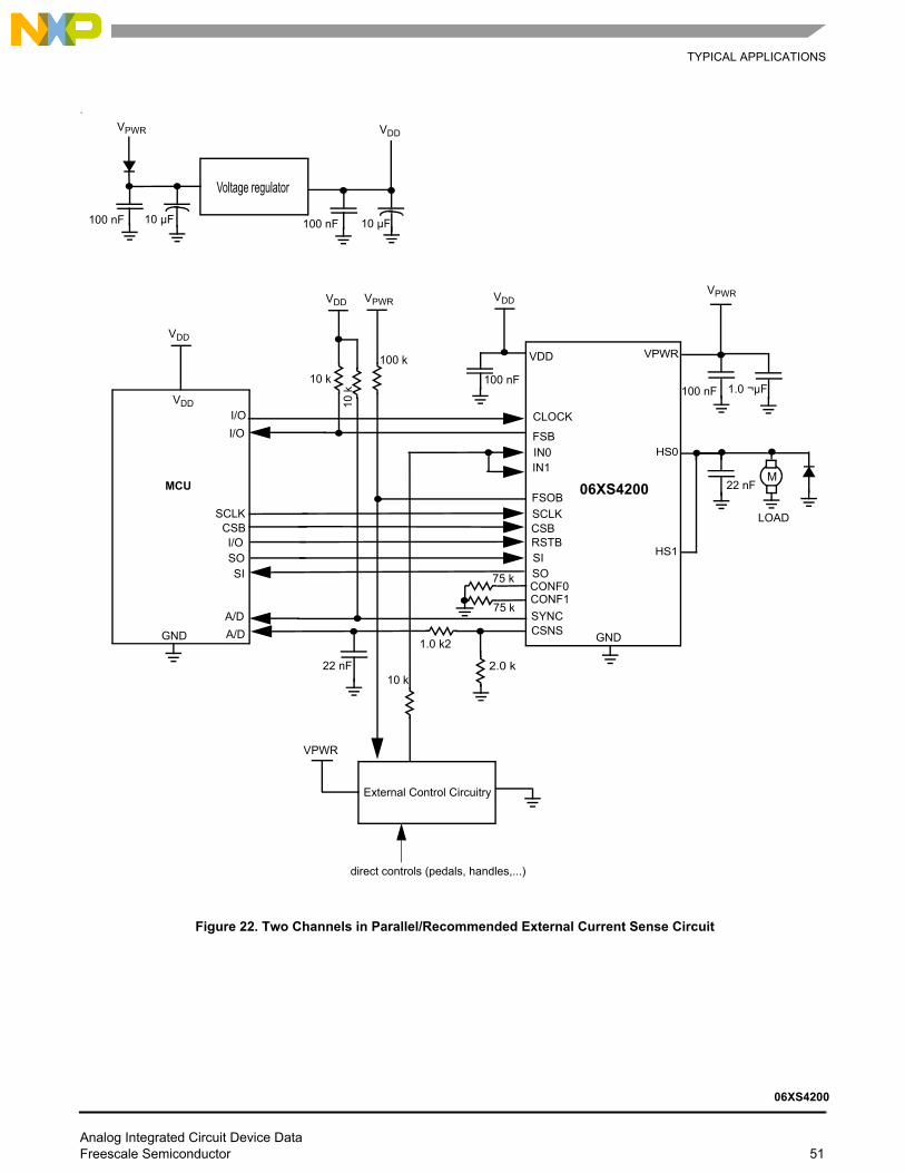
TYPICAL APPLICATIONS
.
Figure 22. Two Channels in Parallel/Recommended External Current Sense Circuit
VDD
GND
MCU
HS0
HS1
VPWRVDD
CLOCK
FSBIN0
SCLKCSB
SISO
RSTB
IN1
100 nF
I/O
I/O
SCLKCSB
SISO
LOAD
CSNSA/D
VDD
VDD
VPWRVDD
22 nF
22 nF 2.0 k
VPWR
100 nF
10 k
FSOB
10 k
VPWR
100 k
M
CONF1CONF0
direct controls (pedals, handles,...)
GND
SYNCA/D
I/O
10k
06XS4200
1.0 k2
75 k
75 k
1.0 µF
External Control Circuitry
VDD
Voltage regulator
VPWR
10 µF100 nF10 µF100 nF
Analog Integrated Circuit Device Data Freescale Semiconductor 51
06XS4200

PACKAGINGSOLDERING INFORMATION
PACKAGING
SOLDERING INFORMATION
The 06XS4200 is packaged in a surface mount power package (PQFN), intended to be soldered directly on the printed circuit board.
The maximum peak temperature during the soldering process should not exceed 260 °C for 10 seconds maximum duration.
The AN2467 provides guidelines for Printed Circuit Board design and assembly.
MARKING INFORMATION
The device is identified by the part number: 06XS4200.Device markings indicate information on the week and
year of manufacturing. The date is coded with the last four characters of the nine character build information
code (e.g. “CTKAH0929”). The date is coded as four numerical digits where the first two digits indicate the year and the last two digits indicate the week. For instance, the date code “0929” indicates the 29th week of the year 2009.
PACKAGE MECHANICAL DIMENSIONS
Package dimensions are provided in package drawings. To find the most current package outline drawing, go to
www.freescale.com and perform a keyword search for the drawing’s document number.
Package Suffix Package Outline Drawing Number23-Pin PQFN FK 98ASA00428D
Analog Integrated Circuit Device Data 52 Freescale Semiconductor
06XS4200
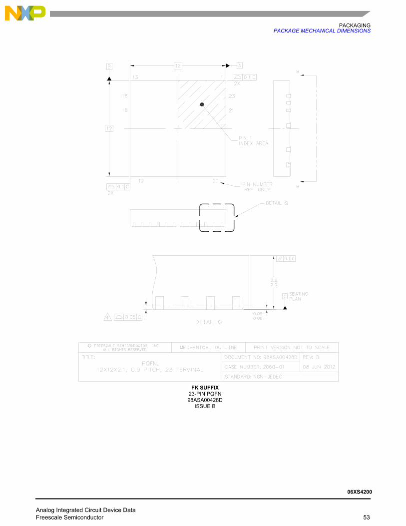
PACKAGINGPACKAGE MECHANICAL DIMENSIONS
FK SUFFIX 23-PIN PQFN98ASA00428D
ISSUE B
Analog Integrated Circuit Device Data Freescale Semiconductor 53
06XS4200

PACKAGINGPACKAGE MECHANICAL DIMENSIONS
FK SUFFIX 23-PIN PQFN98ASA00428D
ISSUE B
Analog Integrated Circuit Device Data 54 Freescale Semiconductor
06XS4200

PACKAGINGPACKAGE MECHANICAL DIMENSIONS
FK SUFFIX 23-PIN PQFN98ASA00428D
ISSUE B
Analog Integrated Circuit Device Data Freescale Semiconductor 55
06XS4200
PACKAGINGPACKAGE MECHANICAL DIMENSIONS
FK SUFFIX 23-PIN PQFN98ASA00428D
ISSUE B
Analog Integrated Circuit Device Data 56 Freescale Semiconductor
06XS4200

PACKAGINGPACKAGE MECHANICAL DIMENSIONS
FK SUFFIX 23-PIN PQFN98ASA00428D
ISSUE B
Analog Integrated Circuit Device Data Freescale Semiconductor 57
06XS4200

PACKAGINGPACKAGE MECHANICAL DIMENSIONS
FK SUFFIX 23-PIN PQFN98ASA00428D
ISSUE B
Analog Integrated Circuit Device Data 58 Freescale Semiconductor
06XS4200

PACKAGINGPACKAGE MECHANICAL DIMENSIONS
FK SUFFIX 23-PIN PQFN98ASA00428D
ISSUE B
Analog Integrated Circuit Device Data Freescale Semiconductor 59
06XS4200

PACKAGINGPACKAGE MECHANICAL DIMENSIONS
FK SUFFIX 23-PIN PQFN98ASA00428D
ISSUE B
Analog Integrated Circuit Device Data 60 Freescale Semiconductor
06XS4200

REVISION HISTORY
REVISION HISTORY
REVISION DATE DESCRIPTION OF CHANGES
1.0 8/2012 • Initial Release
2.0 5/2013 • Grammatical accuracy and form consistency changes made. No changes to content• Revised back page. Updated document properties. Added SMARTMOS sentence to first paragraph
3.0 4/2014 • Added an Orderable Parts table• Added 06XS4200BFK to the ordering information• Introduction of parameters related to 06XS4200B device (Table 1).• Removed RDSON values at 1.0 A.• Rectification of the inversion between ∆tDLY values at slow and medium slew rate.• Removed ECl_rep values• Change the ECl_sing value• New VD_GND clamp value for 06XS4200B
4.0 4/2014 • No technical changes. Revised back page. Updated document properties.
Analog Integrated Circuit Device Data Freescale Semiconductor 61
06XS4200

Document Number: MC06XS4200Rev. 4.0
4/2014
Information in this document is provided solely to enable system and software implementers to use Freescale products.
There are no express or implied copyright licenses granted hereunder to design or fabricate any integrated circuits based
on the information in this document.
Freescale reserves the right to make changes without further notice to any products herein. Freescale makes no
warranty, representation, or guarantee regarding the suitability of its products for any particular purpose, nor does
Freescale assume any liability arising out of the application or use of any product or circuit, and specifically disclaims any
and all liability, including without limitation consequential or incidental damages. “Typical” parameters that may be
provided in Freescale data sheets and/or specifications can and do vary in different applications, and actual performance
may vary over time. All operating parameters, including “typicals,” must be validated for each customer application by
customer’s technical experts. Freescale does not convey any license under its patent rights nor the rights of others.
Freescale sells products pursuant to standard terms and conditions of sale, which can be found at the following address:
freescale.com/SalesTermsandConditions.
Freescale and the Freescale logo are trademarks of Freescale Semiconductor, Inc., Reg. U.S. Pat. & Tm. Off.
SMARTMOS is a trademark of Freescale Semiconductor, Inc. All other product or service names are the property of their
respective owners.
© 2014 Freescale Semiconductor, Inc.
How to Reach Us:Home Page: freescale.com
Web Support: freescale.com/support
Related Documents