Maximizing tandem solar cell power extraction using a three-terminal design Journal: Sustainable Energy & Fuels Manuscript ID SE-COM-03-2018-000133 Article Type: Communication Date Submitted by the Author: 16-Mar-2018 Complete List of Authors: Warren, Emily; California Institute of Technology, Deceglie, Michael; National Renewable Energy Laboratory Rienäcker, Michael; Institut fur Solarenergieforschung GmbH, Photovoltaics Peibst, Robby; Institut fur Solarenergieforschung GmbH Tamboli, Adele; National Renewable Energy Lab, ; Colorado School of Mines, Physics Stradins, Paul; National Renewable Energy Laboratory, National Center for Photovoltaics Sustainable Energy & Fuels

Welcome message from author
This document is posted to help you gain knowledge. Please leave a comment to let me know what you think about it! Share it to your friends and learn new things together.
Transcript

Maximizing tandem solar cell power extraction using a
three-terminal design
Journal: Sustainable Energy & Fuels
Manuscript ID SE-COM-03-2018-000133
Article Type: Communication
Date Submitted by the Author: 16-Mar-2018
Complete List of Authors: Warren, Emily; California Institute of Technology, Deceglie, Michael; National Renewable Energy Laboratory Rienäcker, Michael; Institut fur Solarenergieforschung GmbH, Photovoltaics Peibst, Robby; Institut fur Solarenergieforschung GmbH Tamboli, Adele; National Renewable Energy Lab, ; Colorado School of Mines, Physics Stradins, Paul; National Renewable Energy Laboratory, National Center for Photovoltaics
Sustainable Energy & Fuels
Journal Name
Maximizing tandem solar cell power extraction using athree-terminal design†
Emily L. Warren,∗a Michael G. Deceglie,a Michael Reinäcker,b Robby Peibst,b Adele C.Tambolia and Paul Stradins,a
Tandem or multijunction solar cells can greatly increase theefficiency of solar energy conversion by absorbing differentenergies of the incident solar illumination in semiconduc-tors with different band-gaps, which can operate moreefficiently than a single absorber. Many different designsof tandem cells based on high efficiency top cells and Sibottom cells have been proposed, and there is ongoingdebate as to whether the sub-cells should be wired inseries (to create a tandem device with two terminals) oroperated independently (four terminals). An alternativecell configuration that combines some of the strengths ofboth is a three-terminal device consisting of a top cell op-tically in series with a modified interdigitated back contact(IBC) Si cell featuring a conductive top contact. Such aconfiguration can enable improved energy yield while onlyrequiring external wiring on the front and back of the solarcell stack. In this paper, we investigate the operation ofthree terminal tandems in detail using technology computeraided design (TCAD) device physics simulations. Using III-Vtop cells as an example case, we show how the addition ofa third terminal can deliver comparable power output thana four terminal device, and substantially more power thana two-terminal device, while also enabling power injectionand extraction between the two sub-circuits under a varietyof spectral conditions.
1 IntroductionThe field of high-efficiency photovoltaics is experiencing a resur-gence of research in the area of hybrid tandem photovoltaics,where two or more dissimilar materials are combined into onedevice. These tandem cells split the incident solar spectrum into
a National Renewable Energy Lab, Golden, CO, USA; E-mail: [email protected] Institute for Solar Energy Research Hamelin, Emmerthal, Germany† Electronic Supplementary Information (ESI) available: [Simulation parameters,power calculations, experimental comparison]. See DOI: 10.1039/b000000x/
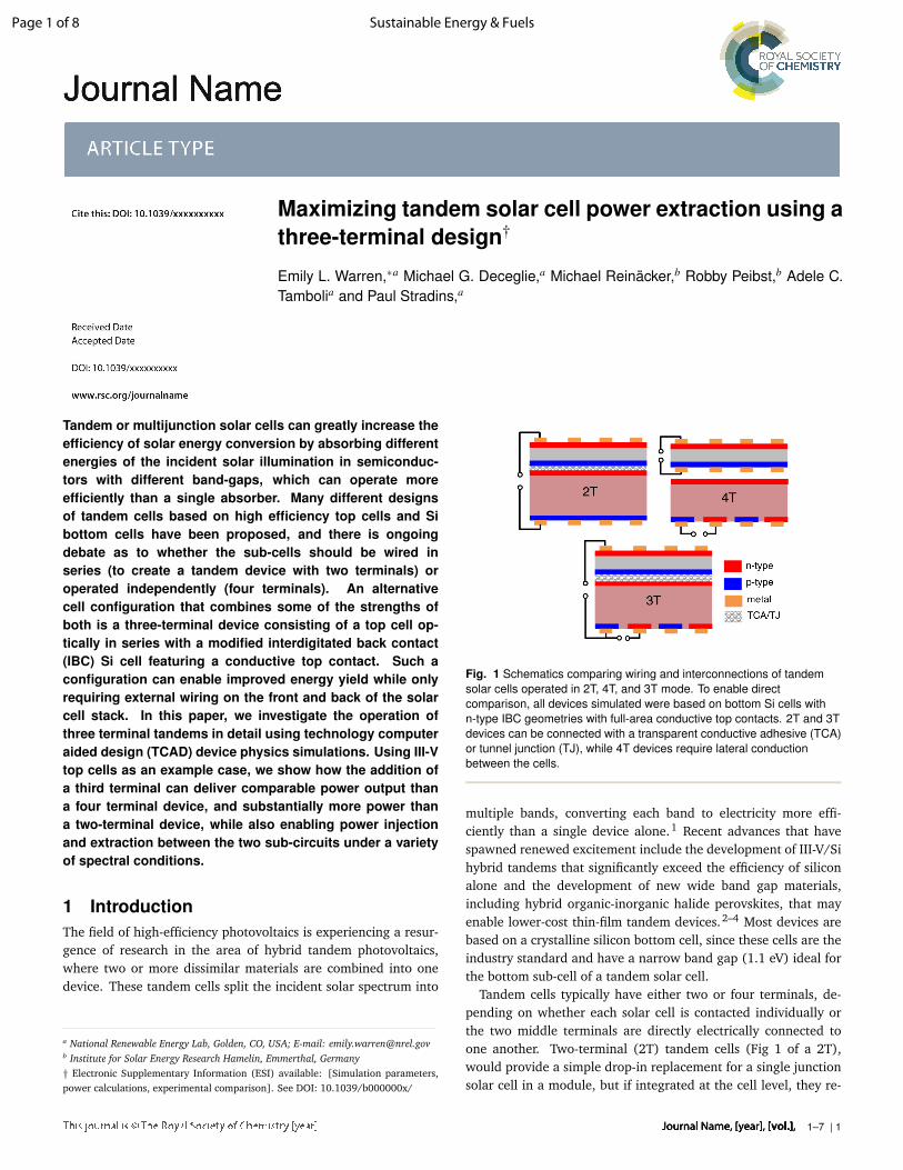
Fig. 1 Schematics comparing wiring and interconnections of tandemsolar cells operated in 2T, 4T, and 3T mode. To enable directcomparison, all devices simulated were based on bottom Si cells withn-type IBC geometries with full-area conductive top contacts. 2T and 3Tdevices can be connected with a transparent conductive adhesive (TCA)or tunnel junction (TJ), while 4T devices require lateral conductionbetween the cells.
multiple bands, converting each band to electricity more effi-ciently than a single device alone.1 Recent advances that havespawned renewed excitement include the development of III-V/Sihybrid tandems that significantly exceed the efficiency of siliconalone and the development of new wide band gap materials,including hybrid organic-inorganic halide perovskites, that mayenable lower-cost thin-film tandem devices.2–4 Most devices arebased on a crystalline silicon bottom cell, since these cells are theindustry standard and have a narrow band gap (1.1 eV) ideal forthe bottom sub-cell of a tandem solar cell.
Tandem cells typically have either two or four terminals, de-pending on whether each solar cell is contacted individually orthe two middle terminals are directly electrically connected toone another. Two-terminal (2T) tandem cells (Fig 1 of a 2T),would provide a simple drop-in replacement for a single junctionsolar cell in a module, but if integrated at the cell level, they re-
Journal Name, [year], [vol.], 1–7 | 1
Page 1 of 8 Sustainable Energy & Fuels

quire current matching of the two sub-cells, which significantlyconstrains the choice of top cell materials. Typically, 2T tandemcells have been realized by monolithic/epitaxial growth or waferbonding. Monolithic growth can be advantageous if high effi-ciency top cells are compatible with growth directly on Si. Inthis approach, the interface between the two cells requires a tun-nel junction or transparent conductive layer with excellent ver-tical conductivity, but no lateral conductivity to extract currentbetween cells. Four-terminal (4T) devices (as shown in Fig. 1of a 4T), in contrast, can be wired together at the cell or modulelevel and thus have considerably more flexibility in top cell choiceand less sensitivity to spectral variations since current matching isnot required.5–7 At the module level they can be integrated as 4Tmodules, or voltage-matched to produce modules with two ter-minals.8 They also are compatible with textured Si bottom cells.However, 4T cells require intermediate grids or transparent con-ductive layers between the cells to transport the current laterallyto the edge of the cells, increasing optical losses. The sub-cellsmust be processed seperately, which is incompatible with mono-lithic growth but can enable integration of materials that haveprocessing incompatibilities. So far, the highest efficiencies havebeen obtained using 4T devices, partially due to the variety of topcells that can be incorporated when the sub-cells do not need tobe current matched.2
Here, we present a third option for hybrid tandem photo-voltaics: a three-terminal (3T) cell based on an interdigitatedback contact (IBC) silicon bottom cell with a conductive top con-nection to a wider bandgap top cell (Fig. 1 of a 3T). This mono-lithic tandem configuration combines the ease of fabrication of a2T device (only requiring external wiring on the front and backof the solar cell stack) with the flexibility and performance of a4T device (lower sensitivity to spectral variations, flexibility inchoice of top-cell bandgap, compatible with textured Si bottomcells). A bottom cell with an IBC geometry and conductive frontsurface field contact enables the use of three terminals wheretwo of the three are on the back of the cell, providing a plat-form for high efficiency 3T cells. Similar 3T devices have beenproposed but not investigated in depth, nor experimentally veri-fied.9–12 For instance, Nagashima et al., proposed tandems basedon combining a III-V top cell with an IBC-Ge or IBC-Si bottom cellso the two subcells share a common base,9,12 while Adhyaksa etal. proposed a 3T tandem based on an IBC-Si cell with a “floatingfront emitter”.11 Prior work by Gee et al.,13 and Schulte-Huxel,14
have demonstrated that it is possible to integrate generic 3T de-vices into modules without significant performance loss. Whilethe prior modeling has shown there is potential for such a de-vice to produce power, some of the previously proposed 3T tan-dem structures have never been simulated with device physicssoftware capable of handling semiconductor devices with morethan two contacts or the electrical connections between multipledevices, which raises questions about their practical feasibility.Here, we describe for the first time the full operation behavior ofsingle junction 3T Si sub-cell, and the complete operating spaceof a 3T tandem device.
The 3T tandem concept presented here is fundamentally dif-ferent from prior “middle contact” 3T approaches that have been
fabricated and used as diagnostic tools to address specific cellsin a multijunction stack.15–18 It is also different from a recentlyproposed “heterojunction bipolar transistor” solar cell that relieson two ideal heterojunction devices to eliminate the need for atunnel junction in a tandem device.19 In contrast, in a 3T-IBCdevice, the Si bottom cell itself has three unique terminals, andtherefore cannot be simply described by existing equivalent cir-cuit models. To fully understand the performance of such a 3Tcell, we have used rigorous technology computer aided design(TCAD) device modeling to investigate the operating principlesof a 3T solar cell both as an independently operated device, andintegrated with a top cell. We show that the addition of the extrabase contact enables the injection or extraction of excess currentin the bottom cell that is present due to current mismatch. Oursimulations agree with experimental measurements of 3T Si de-vices, and have helped with the development of a lumped equiva-lent circuit model (to be published) to describe 3T device behav-ior.20 Although our 3T tandem geometry could be achieved byeither mechanical integration or heteroepitaxial growth, all simu-lations presented here are based on experimentally fabricated de-vices21,22 and realistic interconnection schemes between the cellsbased on transparent conductive adhesives (TCAs),23,24 whichenables simulations to be directly compared to experimental re-sults. This will to help guide the fabrication and optimization of3T tandem cells and modules based on high efficiency top cellssuch as III-Vs or hybrid organic-inorganic halide perovskites.
2 MethodsWe have modeled a 3T device using a two dimensional TCADsoftware package (Sentaurus, Synopsis).25 The Si cell was mod-eled using geometries and doping characteristics based on n-typecarrier-selective polysilicon on oxide (POLO) devices fabricated atISFH (Fig. 2a).26,27 The cell has an n-type (phosphorus doped)base, with interdigitated back contacts consisting of interfacialSiO2 layers coated with heavily doped poly-Si (boron or phos-phorus doped). The entire front surface of the cell has an n-typepoly-Si/SiO2 passivated contact. A series resistance of 0.5 Ω-cm2
was used between the subcells, based on experimentally mea-sured properties of a TCA consisting of Ag-coated microspheresembedded in ethylene-vinyl acetate (EVA).23 A schematic of thesimulated Si unit cell is shown in Figure 2a, and additional detailsof the simulation parameters can be found in the ESI.†
Optical generation profiles were calculated using a Monte Carloray tracing approach that accounts for coherent effects in thinfilms for a variety of input spectra generated with SMARTs.28
Separate profiles were generated for Si cells without top cells andSi cells that operate below a 1 µm thick GaInP cell device stackincluding antireflective coatings, contact layers, and a TCA layer(see ESI for details of the optical simulation).21 To accurately pre-dict the performance of a realistic device, all physical models rec-ommended in a recent review of numerical simulations of Si solarcells by Altermatt were incorporated into the simulation with theexception of Auger recombination, where the improved modelproposed by Richter was implemented.29,30 A two-terminal III-Vtop cell can be accurately described by a single diode model.31 Inthe case of a TCA-interconnected tandem device, the top cell in-
2 | 1–7Journal Name, [year], [vol.],
Page 2 of 8Sustainable Energy & Fuels
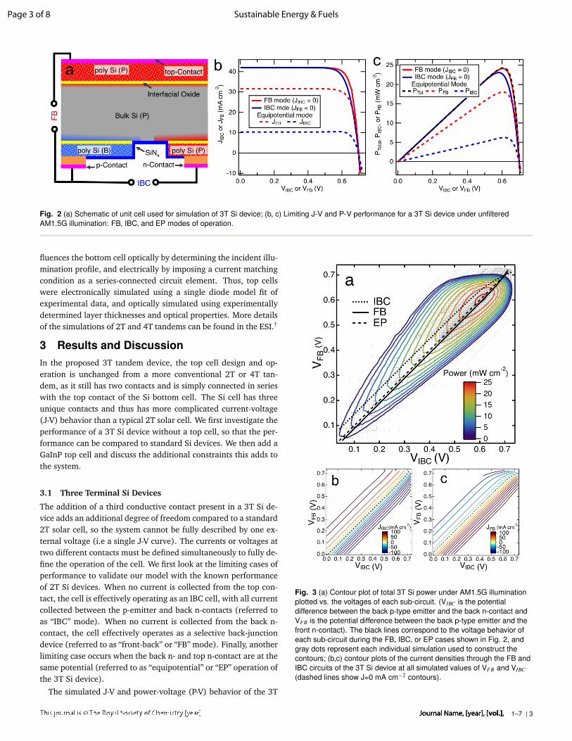
Fig. 2 (a) Schematic of unit cell used for simulation of 3T Si device; (b, c) Limiting J-V and P-V performance for a 3T Si device under unfilteredAM1.5G illumination: FB, IBC, and EP modes of operation.
fluences the bottom cell optically by determining the incident illu-mination profile, and electrically by imposing a current matchingcondition as a series-connected circuit element. Thus, top cellswere electronically simulated using a single diode model fit ofexperimental data, and optically simulated using experimentallydetermined layer thicknesses and optical properties. More detailsof the simulations of 2T and 4T tandems can be found in the ESI.†
3 Results and DiscussionIn the proposed 3T tandem device, the top cell design and op-eration is unchanged from a more conventional 2T or 4T tan-dem, as it still has two contacts and is simply connected in serieswith the top contact of the Si bottom cell. The Si cell has threeunique contacts and thus has more complicated current-voltage(J-V) behavior than a typical 2T solar cell. We first investigate theperformance of a 3T Si device without a top cell, so that the per-formance can be compared to standard Si devices. We then add aGaInP top cell and discuss the additional constraints this adds tothe system.
3.1 Three Terminal Si Devices
The addition of a third conductive contact present in a 3T Si de-vice adds an additional degree of freedom compared to a standard2T solar cell, so the system cannot be fully described by one ex-ternal voltage (i.e a single J-V curve). The currents or voltages attwo different contacts must be defined simultaneously to fully de-fine the operation of the cell. We first look at the limiting cases ofperformance to validate our model with the known performanceof 2T Si devices. When no current is collected from the top con-tact, the cell is effectively operating as an IBC cell, with all currentcollected between the p-emitter and back n-contacts (referred toas “IBC” mode). When no current is collected from the back n-contact, the cell effectively operates as a selective back-junctiondevice (referred to as “front-back” or “FB” mode). Finally, anotherlimiting case occurs when the back n- and top n-contact are at thesame potential (referred to as “equipotential” or “EP” operation ofthe 3T Si device).
The simulated J-V and power-voltage (P-V) behavior of the 3T
Fig. 3 (a) Contour plot of total 3T Si power under AM1.5G illuminationplotted vs. the voltages of each sub-circuit. (VIBC is the potentialdifference between the back p-type emitter and the back n-contact andVFB is the potential difference between the back p-type emitter and thefront n-contact). The black lines correspond to the voltage behavior ofeach sub-circuit during the FB, IBC, or EP cases shown in Fig. 2, andgray dots represent each individual simulation used to construct thecontours; (b,c) contour plots of the current densities through the FB andIBC circuits of the 3T Si device at all simulated values of VFB and VIBC(dashed lines show J=0 mA cm−2 contours).
Journal Name, [year], [vol.], 1–7 | 3
Page 3 of 8 Sustainable Energy & Fuels
Si cell in each of the above limiting cases under AM1.5G illumi-nation (no top III-V cell) is shown in Fig. 2b and 2c to enablecomparison to the performance of a standard Si cell with 2 termi-nals. The 3T Si cell has nearly identical performance operating ineither FB or IBC mode, similar to experimental measurements ofan experimental 3T device (Fig. S2).20 The maximum simulated1-sun efficiency of the device is 24.3%, in good agreement withthe experimentally measured 25.0% efficiency for an IBC POLOdevice without a poly-Si layer at the front of the cell.26 In the sim-ulations, the only difference between the two modes is a slightlylower fill factor in the IBC case, which is likely due to lateral cur-rent transport, current crowding, or higher series resistance at theback n-contact, and could be optimized by changing the geometryor cell design at the rear side of the device.32 In EP mode, a finiteamount of current flows to each of the n-type contacts, creatingtwo separate power producing circuits (dashed lines in Fig. 2b).
To compare all of the different operating states of the cell, itis more useful to plot the total power produced in the cell, byadding the power-voltage curves in each circuit, as the J-V curvesin the two different circuits depend on different voltages. The fulloperation space of a 3T Si device was mapped by explicitly defin-ing the potentials of all of the contacts and fully solving Poisson’sequations over a wide range of values (Fig. 3a). This contourplot show the total power of the system (PFB + PIBC) under stan-dard illumination conditions in the region where the net powerproduction of the cell is positive as a function of VIBC (the po-tential difference between the back p-type emitter and the backn-contact) and VFB (the potential difference between the backp-type emitter and the front n-contact).
For each of the limiting cases (FB, IBC, EP) discussed above,the voltages of each sub-circuit can be represented on the contourplot in Fig. 3a. Even when no current is passing through one ofthe n-type contacts, their potentials are inter-dependent. It caneasily be seen that the highest overall cell performance is achievedfor the EP case where the potentials of the front and back contactsare equal (i.e. VFB = VIBC). At any operating state where thereis a potential difference between the two n-contacts (i.e. VFB 6=VIBC), the overall cell performance decreases due to the excesscurrent flow between the heavily doped contacts (poly-Si/SiO2)through the wafer base. Since the contact and base resistivitiesare relatively low, even a small voltage difference between thetwo contacts leads to significant excess currents (see Fig. 3b,c)and thus to power dissipation within the cell. This takes place inall areas away from the equipotential mode line in Fig. 3a, andexplains why the total efficiency for the two terminal modes ofoperation (FB, IBC) is lower than the EP case.
This ability to have reversible current flow at each n-contacthas a very interesting application for tandem cell performance.In situations where the Si subcell has excess photocurrent rela-tive to the top-cell, adding a third contact enables the extractionof excess photocurrent from the bottom cell. However, under cer-tain conditions this contact can also be used to inject current intothe device. In a situation where the bottom sub-cell in a tandembecomes current limiting, due to a narrower bandgap topcell ora temporary system fluctuation, it would be possible to stabilizethe power output of the 2T tandem circuit by injecting current
!"
#!$
#!"
"!$%&'( )*+*%
,-./0*1*%
&'(23*4%5
"!6"!7"!$"!8"!9"! "!#"!"
%.':(23*4%5
#7
#
;
8
"
),-./0*4<=>?<
5
#! "!;"!8"!"
%@AB-CD*4%5
*#"*
* "*
*9"*
* ;*
* 7*
* 8*
*#7*
*#;*
*#8**# *
*;*
*9 *
*7*
* *
* *
*8*
9" "#""
9E*E-/FD<*0@GDH*4<=*?<I 5
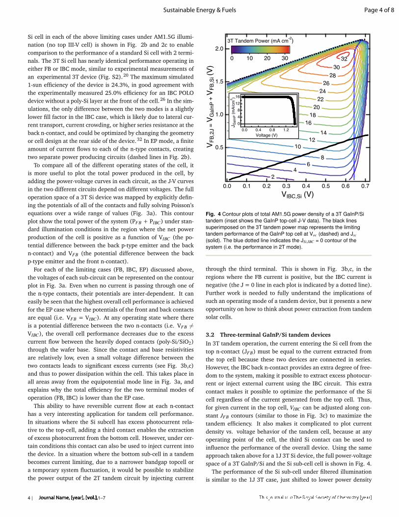
Fig. 4 Contour plots of total AM1.5G power density of a 3T GaInP/Sitandem (inset shows the GaInP top-cell J-V data). The black linessuperimposed on the 3T tandem power map represents the limitingtandem performance of the GaInP top cell at Voc (dashed) and Jsc(solid). The blue dotted line indicates the JSi,IBC = 0 contour of thesystem (i.e. the performance in 2T mode).
through the third terminal. This is shown in Fig. 3b,c, in theregions where the FB current is positive, but the IBC current isnegative (the J = 0 line in each plot is indicated by a dotted line).Further work is needed to fully understand the implications ofsuch an operating mode of a tandem device, but it presents a newopportunity on how to think about power extraction from tandemsolar cells.
3.2 Three-terminal GaInP/Si tandem devicesIn 3T tandem operation, the current entering the Si cell from thetop n-contact (JFB) must be equal to the current extracted fromthe top cell because these two devices are connected in series.However, the IBC back n-contact provides an extra degree of free-dom to the system, making it possible to extract excess photocur-rent or inject external current using the IBC circuit. This extracontact makes it possible to optimize the performance of the Sicell regardless of the current generated from the top cell. Thus,for given current in the top cell, VIBC can be adjusted along con-stant JFB contours (similar to those in Fig. 3c) to maximize thetandem efficiency. It also makes it complicated to plot currentdensity vs. voltage behavior of the tandem cell, because at anyoperating point of the cell, the third Si contact can be used toinfluence the performance of the overall device. Using the sameapproach taken above for a 1J 3T Si device, the full power-voltagespace of a 3T GaInP/Si and the Si sub-cell cell is shown in Fig. 4.
The performance of the Si sub-cell under filtered illuminationis similar to the 1J 3T case, just shifted to lower power density
4 | 1–7Journal Name, [year], [vol.],
Page 4 of 8Sustainable Energy & Fuels

due the lower total photon flux incident upon the sub-cell. How-ever, the addition of a standard GaInP top cell with two terminalsadds constraints to the operation of the overall tandem device.Just as we only analyzed the modes of operation that producepower for the Si device, we also only consider operation of thetandem cell where power is produced, which corresponds to thepower-producing quadrant of the J-V behavior of GaInP top-cellshown in inset. (Note the tandem efficiency calculated here issemi-empirical, as the GaInP top cell performance is based di-rectly on experimental data fit with a diode model.) As a stand-alone 1J device, we showed that it is possible for current to flowin both directions from each of the n-contacts of the 3T Si de-vice (Fig. 2c). In tandem operation, adding a top cell in serieswith the top n-contact adds the constraint that the direction ofcurrent flow in the 2J FB circuit can no longer be reversed andstill produce power, which corresponds to the Voc of the GaInPcell, represented by the dashed black line in Fig. 4. The Jsc ofthe GaInP top cell is also shown (solid black line in Fig. 4) buteven when the 2J FB circuit does not produce power, the Si cellcan still operate in IBC mode. The blue dotted line in Fig. 4shows the JSi,IBC =0 contour which corresponds to the expectedperformance of this system operated as a 2T tandem.
Interestingly, although the photogeneration in the Si cell isgreater than the top cell in a GaInP/Si tandem, there are stillsome operation conditions in Fig. 4 where current is being in-jected into the 2J FB circuit from the Si IBC circuit. When theGaInP top cell is operating under an applied voltage larger thanVmpp, the Si FB sub-circuit can still be current matched to theGaInP by injecting, rather than extracting, current through theSi-IBC circuit (the dashed blue line in Fig. 4 indicates the JSi,IBC
= 0 contour of the system). Although this region of operationdoes not maximize the overall power production of the tandemcell, it hints at the versatility of cell operation under real worldconditions where maximum power point tracking is required.
Although the fully allowable operation space of a 3T GaInP/Sitandem is complex, it is relatively simple to compare the maxi-mum attainable power of the 3T tandem to other potential sub-cell configurations (e.g. current-matched 2T and 4T, Table 1). Forthe 2T case, the system is described by a single J-V curve, makingit straightforward to find the maximum total power of the tandemcell. For 3T tandem cells, the total power production is optimizedwhen the front cell operates at its maximum power point andthe Si IBC circuit is then maximized. For the 4T case, the sub-cells are optimized independently with the Si cell in IBC mode,because the TCA interconnection between the sub-cells does notallow for lateral current extraction from the Si cell front contact,and fingers are not included in the optical ray-tracing model. Inpractice, mechanically stacked 4T devices can use IBC Si cells22,33
or standard front contacted cells, and at a laboratory scale (1 cm2
devices) there is no substantial power loss due to lateral extrac-tion of current through a metal grid in the front-contacted case,2
but these losses are likely to become significant at the modulescale.34
The simulation results shown in Table 1 are in good agreementwith experimental measurements of 4T tandem devices. Recentlyreported mechanically stacked GaInP/Si tandem cells produced
Table 1 Comparing performance of the same GaInP/Si tandem cellconfigured in 2T, 3T, and 4T mode under AM1.5 G illumination simulatedfrom SMARTS (total spectral power 100.45 mW cm−2). For deviceswhere the FB subcircuit includes both subcells, VFB = VGaInP,FB + VSi,FB.
Configuration VFB,mpp VIBC,mpp Jmpp Eff.(mV) (mV) (mA cm−2) (%)
2T (GaInP + Si-FB) 1940 – 15.8 30.64T (GaInP) 1310 – 15.8 20.64T (Si-IBC) – 585 20.2 11.74T (Total) – – – 32.33T (F-B) 1890 – 15.8 29.83T (Si-IBC) – 594 4.49 2.663T (Total) – – – 32.5
a total efficiency of 32.5% using a Si-heterojunction device and31.5% using a POLO IBC device under AM1.5G illumination.2,22
Simulation of a 4T tandem cell with the bottom cell operating inIBC mode under the same spectrum had an efficiency of 32.3%.As shown in Table 1, the simulated efficiency of the 3T tandemactually exceeds the 4T tandem considered here. This is due tothe reduced FF when the Si cell is operated in IBC mode com-pared to that of a cell fully optimized for 4T operation. This mightbe alleviated with optimization of the contact geometries for IBCoperation. By enabling current to flow to both n-type contactssimultaneously, the 3T case is closer to the idealized “EP" modethan independent operation in either 2T mode, giving the slightperformance advantage seen in Table 1.
3.3 Spectral performanceUnder real world conditions, variations in spectrum, temperature,or illumination intensity will impact the performance of a tan-dem solar cell,7,35 and 4T tandem devices have been shown tohave advantages over 2T tandems because there is no current-matching requirement.5 The ability to simultaneously extractpower from two different circuits connected to a 3T Si deviceenables a 3T tandem to maintain the same advantages as a 4Ttandem under varying spectral and illumination intensity condi-tions. If the top cell performance is limited due to fewer availablehigh energy photons, the excess photo-generation in the bottomcell can still be collected through the IBC circuit. To demonstratethis phenomena, we have run tandem device simulations for theGaInP/Si tandem discussed previously under a variety of standardspectra (AM1 - AM5) comparing 2T, 3T, and 4T operation of thesame device. For each simulation, a unique generation profile wascreated with raytracing and the top cell performance was scaledbased on the EQE of experimental devices. Figure 5a compares2T, 3T, and 4T tandem performance for different spectra. Totalcell efficiency is plotted vs. the average photon energy of eachspectrum considered.
The trends in the data on different spectral conditions showthat 2T cells produce significantly less energy as the average pho-ton energy decreases, but 3T cells show the same spectral insen-sitivity as 4T devices. Under higher air masses, the the averagephoton energy of the incident illumination shifts to lower ener-
Journal Name, [year], [vol.], 1–7 | 5
Page 5 of 8 Sustainable Energy & Fuels

14
12
10
8
6
4
2
Si S
ubce
ll Ef
ficie
ncy
(%)
AM1 AM1.5 AM2 AM3 AM4 AM5Incident Spectrum
3T Si (total) 3T Si (F-B) 3T Si (IBC)
a
b
32
30
28
26
24Tand
em E
ffici
ency
(%) 1.84 1.80 1.78 1.74 1.70 1.68
Average Photon Energy (eV)
3T Tandem 4T Tandem 2T Tandem
Fig. 5 (a) Total tandem efficiency for GaInP/Si tandem under differentincident spectra with 2, 3, or 4 terminal interconnections between cells;(b) Efficiency of each component of the 3T Si sub-cell under differentincident spectra.
gies, reducing the photocurrent generated in the GaInP top cell.In 2T mode, the two sub-cells must be current matched, so thetandem performance also decreases. In 4T mode the cells areoperated independently, so the Si is able to convert longer wave-length photons that are not captured by the top cell. In 3T mode,the performance of each sub-circuit in the Si device must be con-sidered (Fig. 5b). While the efficiency of the FB circuit decreasesdue to the current matching requirement with the top cell, theIBC circuit is able collect the excess photocarriers, and actuallybecomes more efficient as the the average photon energy of theincident illumination decreases.
4 Conclusions and OutlookWe have used TCAD simulations to investigate the performanceof 3T Si and GaInP/Si tandem solar cells under a wide range ofoperating conditions. Our simulations are based on realistic ex-perimental parameters for Si and III-V devices and a TCA-basedcell interconnection scheme that does not not require grids be-tween the two sub-cells. This provides guidelines for the futurefabrication of monolithic 3T tandem devices. The behavior of a3T device cannot be described by a simple I-V curve, and there-fore we investigated the full operating space of 3T devices, bothas independent and tandem solar cells. We show that the the-oretical performance of the 3T tandem device considered heremaintains the same spectral advantage over 2T tandem devicesas a 4T tandem. The extra terminal in the 3T Si sub-cell enablesexcess photocurrent to be extracted when the top cell is current
limiting, or injected from an external source if the Si sub-cell be-comes limiting, which may enable power stabilization at the celllevel due to spectral variations, soiling, or degradation of one ofthe sub-cells.
While this work has focused on a specific implementation of awell-characterized top cell, a Si 3T IBC bottom cell has the po-tential to work with a wide range of other top cell materials in atandem device. The 3T IBC design alleviates the current match-ing conditions of a 2T cell, reducing constraints on the bandgapof the top cell and enabling operation in a wide variety of condi-tions. However, it maintains the fabrication advantages of a 2Ttandem, avoiding the need for lateral conduction between the twocells and potentially providing a mechanism to improve the powerconversion of monolithically grown tandem devices that are notcurrent matched. Thus, the design presented here represents apowerful platform for the development of tandem modules, in-corporating the fabrication advantages of a 2T tandem with theperformance advantages of a 4T design.
5 Conflicts of InterestThere are no conflicts to declare.
6 AcknowledgementsThe authors would like to thank Manuel Schnabel, Jake Atkins,Henning Schulte-Huxel, Ana Kavence, and Andrew Tam for help-ful discussions about data analysis and Sentaurus simulations.Dan Friedman provided help with generating illumination usingSMARTs. This work was supported by the U.S. Department ofEnergy under Contract No. DE-AC36-08GO28308 with Alliancefor Sustainable Energy, LLC, the Manager and Operator of theNational Renewable Energy Laboratory. Funding was providedby the U.S. Department of Energy Office of Energy Efficiencyand Renewable Energy Solar Energy Technologies Office underDE- EE00030299. Funding at ISFH was provided by the Ger-man State of Lower Saxony, the German Federal Ministry for Eco-nomics and Energy (BMWi) within the research project “EASi”(FKZ0324040). The U.S. Government retains and the publisher,by accepting the article for publication, acknowledges that theU.S. Government retains a nonexclusive, paid up, irrevocable,worldwide license to publish or reproduce the published form ofthis work, or allow others to do so, for U.S. Government purposes.
References1 Z. J. Yu, M. Leilaeioun and Z. Holman, Nature Energy, 2016, 1, 16137.2 S. Essig, C. Allebé, T. Remo, J. F. Geisz, M. A. Steiner, K. Horowitz, L. Barraud,
J. S. Ward, M. Schnabel, A. Descoeudres, D. L. Young, M. Woodhouse, M. De-speisse, C. Ballif and A. Tamboli, Nature Energy, 2017, 2, 17144.
3 R. Cariou, J. Benick, P. Beutel, N. Razek, C. Fl, M. Hermle, D. Lackner, S. W.Glunz, S. Member, A. W. Bett, M. Wimplinger and F. Dimroth, J. of Photovoltaics,2017, 7, 367–373.
4 K. A. Bush, A. F. Palmstrom, J. Y. Zhengshan, M. Boccard, R. Cheacharoen, J. P.Mailoa, D. P. McMeekin, R. L. Z. Hoye, C. D. Bailie, T. Leijtens and others, NatureEnergy, 2017, 2, 17009.
5 H. Liu, Z. Ren, Z. Liu, A. G. Aberle, T. Buonassisi and I. M. Peters, Optics Express,2015, 23, A382.
6 J. P. Mailoa, M. Lee, I. M. Peters, T. Buonassisi, A. Panchula and D. N. Weiss,Energy Environ. Sci., 2016, 9, 2644–2653.
7 M. T. Horantner and H. J. Snaith, Energy Environ. Sci., 2017.8 S. MacAlpine, D. C. Bobela, S. Kurtz, M. P. Lumb, K. J. Schmieder, J. E. Moore,
R. J. Walters and K. Alberi, Journal of Photonics for Energy, 2017, 7, 1.9 T. Nagashima, K. Okumura, K. Murata and Y. Kimura, Proceedings of the 28th
IEEE PVSC, 2000, pp. 1193–1196.
6 | 1–7Journal Name, [year], [vol.],
Page 6 of 8Sustainable Energy & Fuels

10 J. C. Jimeno, R. Gutierrez, V. Fano, A. Habib, C. del Cañizo, M. A. Rasool andA. Otaegi, Energy Procedia, 2016, 92, 644–651.
11 G. W. P. Adhyaksa, E. Johlin and E. C. Garnett, Nano Letters, 2017, 17, 5206–5212.
12 T. Nagashima, K. Hokoi, K. Okumura and M. Yamaguchi, 2006 IEEE 4th WorldConference on Photovoltaic Energy Conference, 2006, pp. 655–658.
13 J. M. Gee, Solar Cells, 1988, 24, 147–155.14 H. Schulte-Huxel, E. L. Warren, M. Schnabel, P. Stradins, D. J. Friedman and
A. C. Tamboli, Photovoltaic Specialists Conference (PVSC), 2017 IEEE 44rd,2017.
15 N. Ito, T. Uesugi, S. Sakai, M. Umeno and S. Hattori, Japanese Journal ofApplied Physics, 1981, 20, 121–125.
16 M. A. Steiner, M. W. Wanlass, J. J. Carapella, A. Duda, J. S. Ward, T. E. Moriartyand K. A. Emery, Progress in Photovoltaics: Research and Applications, 2009,17, 587–593.
17 T. Soga, M. Yang, T. Jimbo and M. Umeno, Japanese Journal of Applied Physics,1996, 35, 1401–1404.
18 M. Emziane and R. J. Nicholas, Journal of Applied Physics, 2007, 102, year.19 a. Martí and a. Luque, Nature Communications, 2015, 6, 6902.20 M. Rienäcker, E. L. Warren, M. Schabel, H. Schulte-Huxel, A. Merkle, S. Kajari-
Schöder, R. Niepelt, R. Brendel, P. Stradins, A. Tamboli and R. Peibst, In Prep.,2018.
21 J. F. Geisz, M. A. Steiner, I. García, S. R. Kurtz and D. J. Friedman, Appl. Phys.Lett, 2013, 103, 041118.
22 M. Rienäcker, M. Schnabel, E. Warren, H. Merkle, A. andSchulte-Huxel, T. Klein,M. van Hest, M. Steiner, J. Geisz, S. Kajari-Schröder, R. Niepelt, J. Schmidt,R. Brendel, P. Stradins, A. Tamboli and R. Peibst, Proceedings of the 2017 EU-PVSEC, 2017.
23 T. Klein, B. Lee, M. Schnabel, E. Warren, P. Stradins, A. Tamboli and M. F. A. M.van Hest, ACS Applied Materials & Interfaces, 2018, 10, 8086–8091.
24 T. Klein, B. Lee, M. Schnabel, E. Warren, P. Stradins, A. Tamboli and M. vanHest, Proceedings of the 44th IEEE PVSC, 2016.
25 Optimization of Rear Contact Design in Monocrystalline Silicon Solar-Cell Using3D TCAD Simulations, 2011.
26 F. Haase, F. Kiefer, S. Schäfer, C. Kruse, J. Krügener, R. Brendel, and R. Peibst,Japanese Journal of Applied Physics, 2017, 56, 08MB15.
27 M. Rienacker, M. Bossmeyer, A. Merkle, R. Udo, F. Haase, J. Kr, R. Brendel andR. Peibst, J. of Photovoltaics, 2017, 7, 11–18.
28 https://www.pvlighthouse.com.au, last accessed Nov 5, 2017.
29 P. P. Altermatt, Journal of Computational Electronics, 2011, 10, 314–330.30 A. Richter, F. Werner, A. Cuevas, J. Schmidt and S. W. Glunz, Energy Procedia,
2012, pp. 88–94.31 M. Campanelli, http://pv-fit.com/, Oct 16, 2017.32 H. Steinkemper, F. Feldmann, M. Bivour and M. Hermle, IEEE Journal of
Photovoltaics, 2015, 5, 1348–1356.33 M. Schnabel, M. Rienaecker, A. Merkle, T. Klein, N. Jain, S. Essig, M. van
Hest, J. F. Geisz, J. Schmidt, R. Brendel, R. Peibst, P. Stradins and A. Tamboli,Proceedings of the 44th IEEE PVSC, 2017.
34 S. E. Sofia, N. Sahraei, J. P. Mailoa, T. Buonassisi and I. M. Peters, IEEE Journalof Photovoltaics, 2017, 7, 934–940.
35 M. H. Futscher and B. Ehrler, ACS Energy Letters, 2016, 1, 863–868.
7 Table of Contents Entry
IBC
FB
III-V
Si
Fig. 6 Three-terminal tandem solar cells can provide a robust operatingmechanism to efficiently capture the solar spectrum without the need tocurrent match sub-cells or fabricate complicated metal interconnects.
Journal Name, [year], [vol.], 1–7 | 7
Page 7 of 8 Sustainable Energy & Fuels

IBC
FB
III-V
Si
Page 8 of 8Sustainable Energy & Fuels
Related Documents