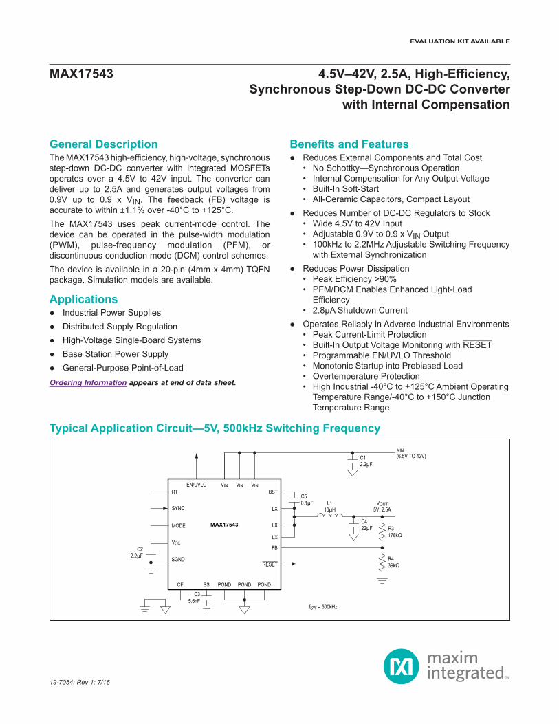
19-7054; Rev 1; 7/16 General Description The MAX17543 high-efficiency, high-voltage, synchronous step-down DC-DC converter with integrated MOSFETs operates over a 4.5V to 42V input. The converter can deliver up to 2.5A and generates output voltages from 0.9V up to 0.9 x V IN . The feedback (FB) voltage is accurate to within ±1.1% over -40°C to +125°C. The MAX17543 uses peak current-mode control. The device can be operated in the pulse-width modulation (PWM), pulse-frequency modulation (PFM), or discontinuous conduction mode (DCM) control schemes. The device is available in a 20-pin (4mm x 4mm) TQFN package. Simulation models are available. Applications ● Industrial Power Supplies ● Distributed Supply Regulation ● High-Voltage Single-Board Systems ● Base Station Power Supply ● General-Purpose Point-of-Load Benefits and Features ● Reduces External Components and Total Cost • No Schottky—Synchronous Operation • Internal Compensation for Any Output Voltage • Built-In Soft-Start • All-Ceramic Capacitors, Compact Layout ● Reduces Number of DC-DC Regulators to Stock • Wide 4.5V to 42V Input • Adjustable 0.9V to 0.9 x V IN Output • 100kHz to 2.2MHz Adjustable Switching Frequency with External Synchronization ● Reduces Power Dissipation • Peak Efficiency >90% • PFM/DCM Enables Enhanced Light-Load Efficiency • 2.8µA Shutdown Current ● Operates Reliably in Adverse Industrial Environments • Peak Current-Limit Protection • Built-In Output Voltage Monitoring with RESET • Programmable EN/UVLO Threshold • Monotonic Startup into Prebiased Load • Overtemperature Protection • High Industrial -40°C to +125°C Ambient Operating Temperature Range/-40°C to +150°C Junction Temperature Range Ordering Information appears at end of data sheet. Typical Application Circuit—5V, 500kHz Switching Frequency RESET VIN VIN VIN BST RT SYNC MODE VCC SGND CF SS FB PGND PGND PGND LX LX LX EN/UVLO MAX17543 L1 10μH C5 0.1μF C4 22μF R3 178kΩ R4 39kΩ VOUT 5V, 2.5A VIN (6.5V TO 42V) C1 2.2μF C3 5.6nF fSW = 500kHz C2 2.2μF MAX17543 4.5V–42V, 2.5A, High-Efficiency, Synchronous Step-Down DC-DC Converter with Internal Compensation EVALUATION KIT AVAILABLE

Welcome message from author
This document is posted to help you gain knowledge. Please leave a comment to let me know what you think about it! Share it to your friends and learn new things together.
Transcript
19-7054; Rev 1; 7/16
General DescriptionThe MAX17543 high-efficiency, high-voltage, synchronous step-down DC-DC converter with integrated MOSFETs operates over a 4.5V to 42V input. The converter can deliver up to 2.5A and generates output voltages from 0.9V up to 0.9 x VIN. The feedback (FB) voltage is accurate to within ±1.1% over -40°C to +125°C.The MAX17543 uses peak current-mode control. The device can be operated in the pulse-width modulation (PWM), pulse-frequency modulation (PFM), or discontinuous conduction mode (DCM) control schemes. The device is available in a 20-pin (4mm x 4mm) TQFN package. Simulation models are available.
Applications Industrial Power Supplies Distributed Supply Regulation High-Voltage Single-Board Systems Base Station Power Supply General-Purpose Point-of-Load
Benefits and Features Reduces External Components and Total Cost
• No Schottky—Synchronous Operation• Internal Compensation for Any Output Voltage• Built-In Soft-Start• All-Ceramic Capacitors, Compact Layout
Reduces Number of DC-DC Regulators to Stock• Wide 4.5V to 42V Input• Adjustable 0.9V to 0.9 x VIN Output• 100kHz to 2.2MHz Adjustable Switching Frequency
with External Synchronization Reduces Power Dissipation
• Peak Efficiency >90%• PFM/DCM Enables Enhanced Light-Load
Efficiency• 2.8µA Shutdown Current
Operates Reliably in Adverse Industrial Environments• Peak Current-Limit Protection• Built-In Output Voltage Monitoring with RESET• Programmable EN/UVLO Threshold• Monotonic Startup into Prebiased Load• Overtemperature Protection• High Industrial -40°C to +125°C Ambient Operating
Temperature Range/-40°C to +150°C Junction Temperature Range
Ordering Information appears at end of data sheet.
Typical Application Circuit—5V, 500kHz Switching Frequency
RESET
VIN VIN VINBSTRT
SYNC
MODE
VCC
SGND
CF SS
FB
PGNDPGNDPGND
LX
LX
LX
EN/UVLO
MAX17543
L110µH
C50.1µF
C422µF R3
178kΩ
R439kΩ
VOUT5V, 2.5A
VIN(6.5V TO 42V)C1
2.2µF
C35.6nF
fSW = 500kHz
C22.2µF
MAX17543 4.5V–42V, 2.5A, High-Efficiency, Synchronous Step-Down DC-DC Converter
with Internal Compensation
EVALUATION KIT AVAILABLE
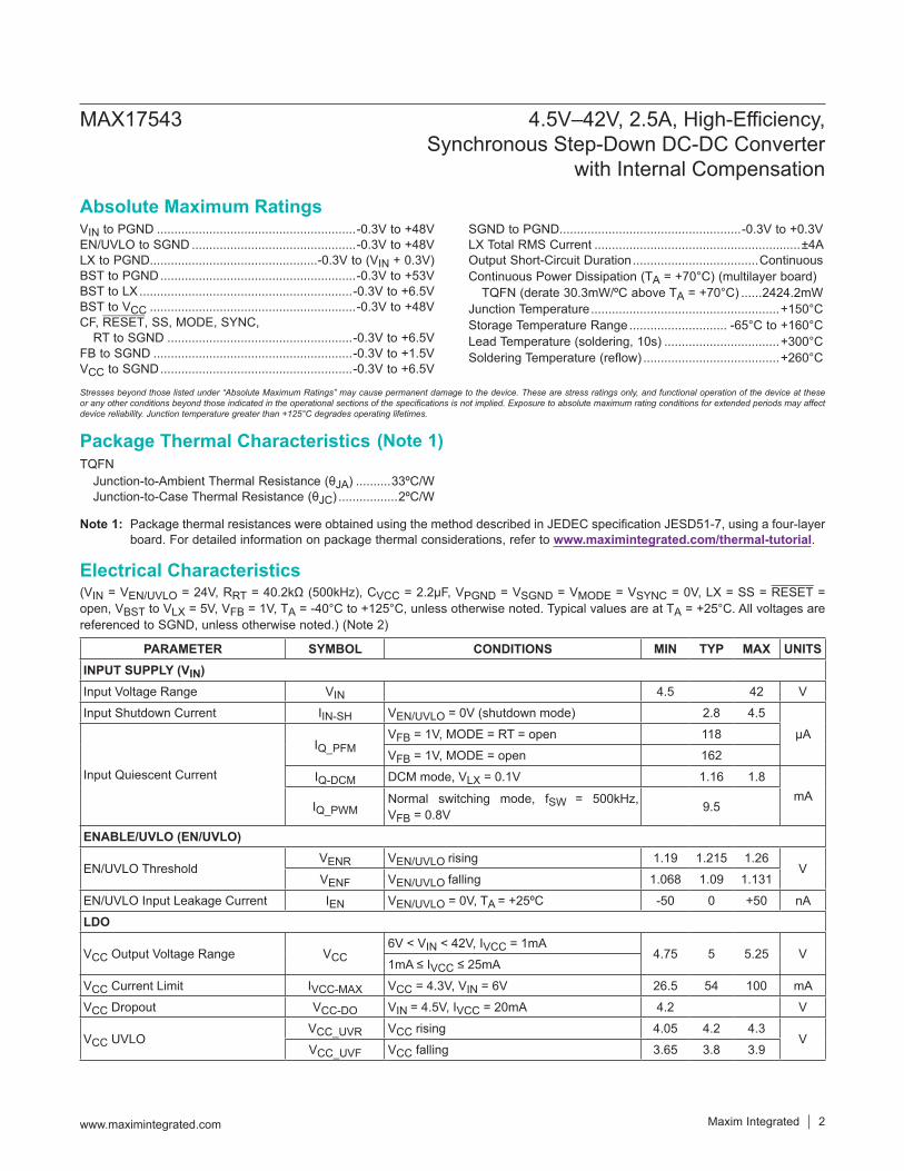
VIN to PGND .........................................................-0.3V to +48VEN/UVLO to SGND ...............................................-0.3V to +48VLX to PGND................................................-0.3V to (VIN + 0.3V)BST to PGND ........................................................-0.3V to +53VBST to LX .............................................................-0.3V to +6.5VBST to VCC ...........................................................-0.3V to +48VCF, RESET, SS, MODE, SYNC,
RT to SGND .....................................................-0.3V to +6.5VFB to SGND .........................................................-0.3V to +1.5VVCC to SGND .......................................................-0.3V to +6.5V
SGND to PGND ....................................................-0.3V to +0.3VLX Total RMS Current ...........................................................±4AOutput Short-Circuit Duration ....................................ContinuousContinuous Power Dissipation (TA = +70°C) (multilayer board) TQFN (derate 30.3mW/ºC above TA = +70°C) ......2424.2mWJunction Temperature ......................................................+150°CStorage Temperature Range ............................ -65°C to +160°CLead Temperature (soldering, 10s) .................................+300°CSoldering Temperature (reflow) .......................................+260°C
TQFN Junction-to-Ambient Thermal Resistance (θJA) ..........33ºC/W Junction-to-Case Thermal Resistance (θJC) .................2ºC/W
(Note 1)
(VIN = VEN/UVLO = 24V, RRT = 40.2kΩ (500kHz), CVCC = 2.2μF, VPGND = VSGND = VMODE = VSYNC = 0V, LX = SS = RESET = open, VBST to VLX = 5V, VFB = 1V, TA = -40°C to +125°C, unless otherwise noted. Typical values are at TA = +25°C. All voltages are referenced to SGND, unless otherwise noted.) (Note 2)
Electrical Characteristics
Note 1: Package thermal resistances were obtained using the method described in JEDEC specification JESD51-7, using a four-layer board. For detailed information on package thermal considerations, refer to www.maximintegrated.com/thermal-tutorial.
Package Thermal Characteristics
Stresses beyond those listed under “Absolute Maximum Ratings” may cause permanent damage to the device. These are stress ratings only, and functional operation of the device at these or any other conditions beyond those indicated in the operational sections of the specifications is not implied. Exposure to absolute maximum rating conditions for extended periods may affect device reliability. Junction temperature greater than +125°C degrades operating lifetimes.
Absolute Maximum Ratings
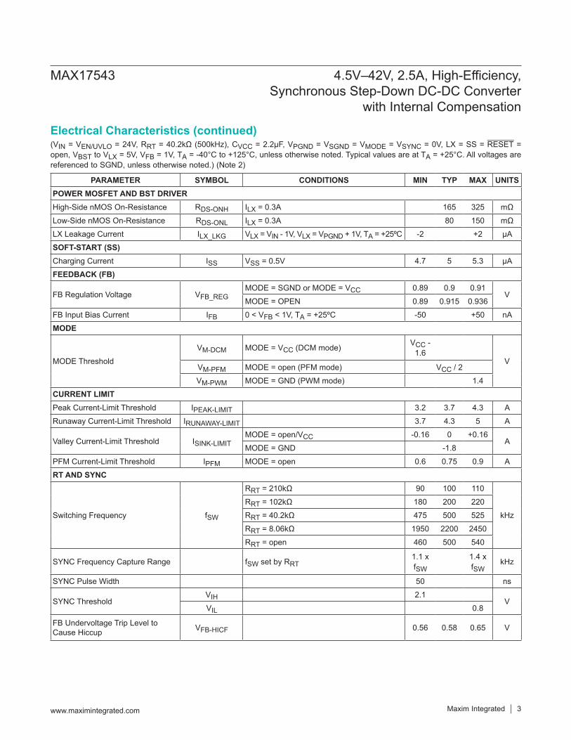
PARAMETER SYMBOL CONDITIONS MIN TYP MAX UNITSINPUT SUPPLY (VIN)Input Voltage Range VIN 4.5 42 VInput Shutdown Current IIN-SH VEN/UVLO = 0V (shutdown mode) 2.8 4.5
µA
Input Quiescent Current
IQ_PFMVFB = 1V, MODE = RT = open 118VFB = 1V, MODE = open 162
IQ-DCM DCM mode, VLX = 0.1V 1.16 1.8mA
IQ_PWMNormal switching mode, fSW = 500kHz, VFB = 0.8V 9.5
ENABLE/UVLO (EN/UVLO)
EN/UVLO ThresholdVENR VEN/UVLO rising 1.19 1.215 1.26
VVENF VEN/UVLO falling 1.068 1.09 1.131
EN/UVLO Input Leakage Current IEN VEN/UVLO = 0V, TA = +25ºC -50 0 +50 nALDO
VCC Output Voltage Range VCC6V < VIN < 42V, IVCC = 1mA
4.75 5 5.25 V1mA ≤ IVCC ≤ 25mA
VCC Current Limit IVCC-MAX VCC = 4.3V, VIN = 6V 26.5 54 100 mAVCC Dropout VCC-DO VIN = 4.5V, IVCC = 20mA 4.2 V
VCC UVLO VCC_UVR VCC rising 4.05 4.2 4.3
VVCC_UVF VCC falling 3.65 3.8 3.9
MAX17543 4.5V–42V, 2.5A, High-Efficiency,Synchronous Step-Down DC-DC Converter
with Internal Compensation
www.maximintegrated.com Maxim Integrated 2
(VIN = VEN/UVLO = 24V, RRT = 40.2kΩ (500kHz), CVCC = 2.2μF, VPGND = VSGND = VMODE = VSYNC = 0V, LX = SS = RESET = open, VBST to VLX = 5V, VFB = 1V, TA = -40°C to +125°C, unless otherwise noted. Typical values are at TA = +25°C. All voltages are referenced to SGND, unless otherwise noted.) (Note 2)
Electrical Characteristics (continued)
PARAMETER SYMBOL CONDITIONS MIN TYP MAX UNITSPOWER MOSFET AND BST DRIVERHigh-Side nMOS On-Resistance RDS-ONH ILX = 0.3A 165 325 mΩLow-Side nMOS On-Resistance RDS-ONL ILX = 0.3A 80 150 mΩLX Leakage Current ILX_LKG VLX = VIN - 1V, VLX = VPGND + 1V, TA = +25ºC -2 +2 µASOFT-START (SS)Charging Current ISS VSS = 0.5V 4.7 5 5.3 µAFEEDBACK (FB)
FB Regulation Voltage VFB_REGMODE = SGND or MODE = VCC 0.89 0.9 0.91
VMODE = OPEN 0.89 0.915 0.936
FB Input Bias Current IFB 0 < VFB < 1V, TA = +25ºC -50 +50 nAMODE
MODE Threshold VM-DCM MODE = VCC (DCM mode) VCC -
1.6V
VM-PFM MODE = open (PFM mode) VCC / 2VM-PWM MODE = GND (PWM mode) 1.4
CURRENT LIMITPeak Current-Limit Threshold IPEAK-LIMIT 3.2 3.7 4.3 ARunaway Current-Limit Threshold IRUNAWAY-LIMIT 3.7 4.3 5 A
Valley Current-Limit Threshold ISINK-LIMITMODE = open/VCC -0.16 0 +0.16
AMODE = GND -1.8
PFM Current-Limit Threshold IPFM MODE = open 0.6 0.75 0.9 ART AND SYNC
Switching Frequency fSW
RRT = 210kΩ 90 100 110
kHzRRT = 102kΩ 180 200 220RRT = 40.2kΩ 475 500 525RRT = 8.06kΩ 1950 2200 2450RRT = open 460 500 540
SYNC Frequency Capture Range fSW set by RRT1.1 x fSW
1.4 x fSW
kHz
SYNC Pulse Width 50 ns
SYNC ThresholdVIH 2.1
VVIL 0.8
FB Undervoltage Trip Level to Cause Hiccup VFB-HICF 0.56 0.58 0.65 V
MAX17543 4.5V–42V, 2.5A, High-Efficiency,Synchronous Step-Down DC-DC Converter
with Internal Compensation
www.maximintegrated.com Maxim Integrated 3
(VIN = VEN/UVLO = 24V, RRT = 40.2kΩ (500kHz), CVCC = 2.2μF, VPGND = VSGND = VMODE = VSYNC = 0V, LX = SS = RESET = open, VBST to VLX = 5V, VFB = 1V, TA = -40°C to +125°C, unless otherwise noted. Typical values are at TA = +25°C. All voltages are referenced to SGND, unless otherwise noted.) (Note 2)
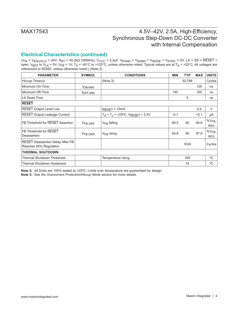
Note 2: All limits are 100% tested at +25ºC. Limits over temperature are guaranteed by design.Note 3: See the Overcurrent Protection/Hiccup Mode section for more details.
Electrical Characteristics (continued)
PARAMETER SYMBOL CONDITIONS MIN TYP MAX UNITSHiccup Timeout (Note 3) 32,768 CyclesMinimum On-Time tON-MIN 135 nsMinimum Off-Time tOFF-MIN 140 160 nsLX Dead Time 5 nsRESETRESET Output Level Low IRESET = 10mA 0.4 VRESET Output Leakage Current TA = TJ = +25ºC, VRESET = 5.5V -0.1 +0.1 µA
FB Threshold for RESET Assertion VFB-OKF VFB falling 90.5 92 94.6 %VFB-REG
FB Threshold for RESET Deassertion VFB-OKR VFB rising 93.8 95 97.8 %VFB-
REG
RESET Deassertion Delay After FB Reaches 95% Regulation 1024 Cycles
THERMAL SHUTDOWNThermal Shutdown Threshold Temperature rising 165 ºCThermal Shutdown Hysteresis 10 ºC
MAX17543 4.5V–42V, 2.5A, High-Efficiency,Synchronous Step-Down DC-DC Converter
with Internal Compensation
www.maximintegrated.com Maxim Integrated 4
(VIN = VEN/UVLO = 24V, VPGND = VSGND = 0V, CVIN = CVCC = 2.2µF, CBST = 0.1µF, CSS = 5600pF, RT = MODE = open, TA = -40°C to +125°C, unless otherwise noted. Typical values are at TA = +25°C. All voltages are referenced to GND, unless otherwise noted.)
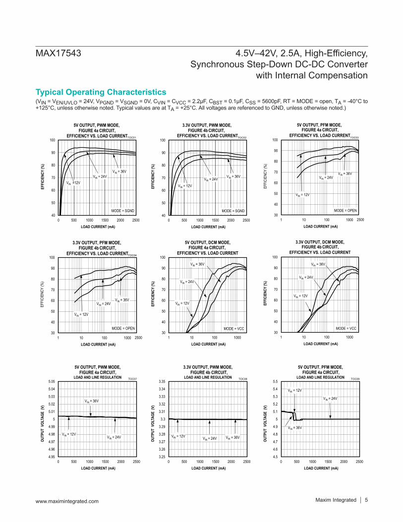
Typical Operating Characteristics
40
50
60
70
80
90
100
0 500 1000 1500 2000 2500
EFFI
CIEN
CY(%
)
LOAD CURRENT (mA)
5V OUTPUT, PWM MODE,IFIGURE 4a C RCUIT,
EFFICIENCY VS. LOAD CURRENT
VIN = 36VVIN = 24V
VIN =12V
MODE = SGND
TOC01
40
50
60
70
80
90
100
0 500 1000 1500 2000 2500
EFFI
CIEN
CY(%
)
LOAD CURRENT (mA)
3.3V OUTPUT, PWM MODE,
EFFICIENCY VS. LOAD CURRENT
VIN = 36VVIN = 24V
VIN = 12V
MODE = SGND
TOC02
FIGURE 4b C RCUIT,I
30
40
50
60
70
80
90
100
1 10 100 1000
EFFI
CIE
NC
Y(%
)
LOAD CURRENT (mA)
5V OUTPUT, PFM MODE,
EFFICIENCY VS. LOAD CURRENT
VIN = 36VVIN = 24V
VIN = 12V
MODE = OPEN
2500
TOC03
FIGURE 4a C RCUIT,I
30
40
50
60
70
80
90
100
1 10 100 1000
EFFI
CIE
NC
Y(%
)
LOAD CURRENT (mA)
3.3V OUTPUT, PFM MODE,FIGURE 4 CIRCUIT,
EFFICIENCY VS. LOAD CURRENT
VIN = 36VVIN = 24V
VIN = 12V
MODE = OPEN
2500
TOC04
FIGURE 4b C RCUIT,I
30
40
50
60
70
80
90
100
1 10 100 1000
EFFI
CIEN
CY(%
)
LOAD CURRENT (mA)
5V OUTPUT, DCM MODE,FIGURE 3 CIRCUIT,
EFFICIENCY VS. LOAD CURRENT
VIN = 36V
VIN = 24V
VIN = 12V
MODE = VCC
FIGURE 4a C RCUIT,I
30
40
50
60
70
80
90
100
1 10 100 1000
EFFIC
IENC
Y(%
)
LOAD CURRENT (mA)
3.3V OUTPUT, DCM MODE,FIGURE 4 CIRCUIT,
EFFICIENCY VS. LOAD CURRENT
VIN = 36V
VIN = 24V
VIN = 12V
MODE = VCC
FIGURE 4b C RCUIT,I
4.95
4.96
4.97
4.98
4.99
5
5.01
5.02
5.03
5.04
5.05
0 500 1000 1500 2000 2500
OUTP
UTVO
LTAG
E(V
)
LOAD CURRENT (mA)
5V OUTPUT, PWM MODE,FIGURE 3 CIRCUIT,
LOAD AND LINE REGULATION
VIN = 36V
VIN = 24VVIN = 12V
TOC07
FIGURE 4a C RCUIT,I
3.25
3.26
3.27
3.28
3.29
3.3
3.31
3.32
3.33
3.34
3.35
0 500 1000 1500 2000 2500
OUTP
UTVO
LTAG
E(V
)
LOAD CURRENT (mA)
3.3V OUTPUT, PWM MODE,FIGURE 4b CIRCUIT,
LOAD AND LINE REGULATION
VIN = 36VVIN = 24VVIN = 12V
TOC08
4.5
4.6
4.7
4.8
4.9
5
5.1
5.2
5.3
5.4
5.5
0 500 1000 1500 2000 2500
OUTP
UTVO
LTAG
E(V
)
LOAD CURRENT (mA)
5V OUTPUT, PFM MODE,FIGURE 3 CIRCUIT,
LOAD AND LINE REGULATION
VIN = 36V
VIN = 24V
VIN = 12V
TOC09
FIGURE 4a C RCUIT,I
Maxim Integrated 5www.maximintegrated.com
MAX17543 4.5V–42V, 2.5A, High-Efficiency,Synchronous Step-Down DC-DC Converter
with Internal Compensation
(VIN = VEN/UVLO = 24V, VPGND = VSGND = 0V, CVIN = CVCC = 2.2µF, CBST = 0.1µF, CSS = 5600pF, RT = MODE = open, TA = -40°C to +125°C, unless otherwise noted. Typical values are at TA = +25°C. All voltages are referenced to GND, unless otherwise noted.)
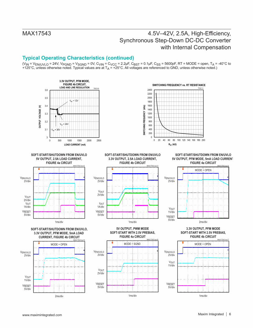
Typical Operating Characteristics (continued)
3
3.1
3.2
3.3
3.4
3.5
3.6
0 500 1000 1500 2000 2500
OUTP
UTVO
LTAG
E(V
)
LOAD CURRENT (mA)
3.3V OUTPUT, PFM MODE,FIGURE 4 CIRCUIT,
LOAD AND LINE REGULATION
VIN = 36V
VIN = 12V
VIN = 24V
TOC10
FIGURE 4b C RCUIT,I
0
200
400
600
800
1000
1200
1400
1600
1800
2000
2200
2400
0 20 40 60 80 100 120 140 160 180 200
SWIT
CHIN
G FR
EQUE
NCY
(kHz
)RRT (kΩ)
SWITCHING FREQUENCY vs. RT RESISTANCETOC11
SOFT-START/SHUTDOWN FROM EN/UVLO5V OUTPUT, 2.5A LOAD CURRENT,
FIGURE 4a CIRCUITMAX17543 toc12
VRESET5V/div
IOUT1A/div
VOUT2V/div
VEN/UVLO2V/div
1ms/div
SOFT-START/SHUTDOWN FROM EN/UVLO3.3V OUTPUT, 2.5A LOAD CURRENT,
FIGURE 4b CIRCUITMAX17543 toc13
VRESET5V/div
IOUT1A/div
VOUT2V/div
VEN/UVLO2V/div
1ms/div
SOFT-START/SHUTDOWN FROM EN/UVLO5V OUTPUT, PFM MODE, 5mA LOAD CURRENT,
FIGURE 4a CIRCUITMAX17543 toc14
VRESET5V/div
VOUT1V/div
VEN/UVLO2V/div
2ms/div
MODE = OPEN
SOFT-START/SHUTDOWN FROM EN/UVLO,3.3V OUTPUT, PFM MODE, 5mA LOAD
CURRENT, FIGURE 4b CIRCUITMAX17543 toc15
VRESET5V/div
VOUT1V/div
VEN/UVLO2V/div
2ms/div
MODE = OPEN
5V OUTPUT, PWM MODESOFT-START WITH 2.5V PREBIAS,
FIGURE 4a CIRCUITMAX17543 toc16
VRESET5V/div
VOUT2V/div
VEN/UVLO2V/div
1ms/div
MODE = SGND
3.3V OUTPUT, PFM MODESOFT-START WITH 2.5V PREBIAS,
FIGURE 4b CIRCUITMAX17543 toc17
VRESET5V/div
VOUT1V/div
VEN/UVLO2V/div
1ms/div
MODE = OPEN
Maxim Integrated 6www.maximintegrated.com
MAX17543 4.5V–42V, 2.5A, High-Efficiency,Synchronous Step-Down DC-DC Converter
with Internal Compensation
(VIN = VEN/UVLO = 24V, VPGND = VSGND = 0V, CVIN = CVCC = 2.2µF, CBST = 0.1µF, CSS = 5600pF, RT = MODE = open, TA = -40°C to +125°C, unless otherwise noted. Typical values are at TA = +25°C. All voltages are referenced to GND, unless otherwise noted.)
Typical Operating Characteristics (continued)
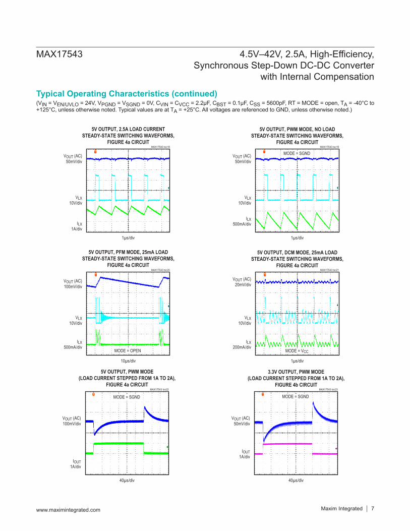
5V OUTPUT, 2.5A LOAD CURRENTSTEADY-STATE SWITCHING WAVEFORMS,
FIGURE 4a CIRCUITMAX17543 toc18
ILX1A/div
VLX10V/div
VOUT (AC)50mV/div
1µs/div
5V OUTPUT, PFM MODE, 25mA LOADSTEADY-STATE SWITCHING WAVEFORMS,
FIGURE 4a CIRCUITMAX17543 toc20
ILX500mA/div
VLX10V/div
VOUT (AC)100mV/div
10µs/div
MODE = OPEN
5V OUTPUT, PWM MODE(LOAD CURRENT STEPPED FROM 1A TO 2A),
FIGURE 4a CIRCUITMAX17543 toc22
IOUT1A/div
VOUT (AC)100mV/div
40µs/div
MODE = SGND
5V OUTPUT, PWM MODE, NO LOADSTEADY-STATE SWITCHING WAVEFORMS,
FIGURE 4a CIRCUITMAX17543 toc19
ILX500mA/div
VLX10V/div
VOUT (AC)50mV/div
1µs/div
MODE = SGND
5V OUTPUT, DCM MODE, 25mA LOADSTEADY-STATE SWITCHING WAVEFORMS,
FIGURE 4a CIRCUITMAX17543 toc21
ILX200mA/div
VLX10V/div
VOUT (AC)20mV/div
1µs/div
MODE = VCC
3.3V OUTPUT, PWM MODE(LOAD CURRENT STEPPED FROM 1A TO 2A),
FIGURE 4b CIRCUITMAX17543 toc23
IOUT1A/div
VOUT (AC)50mV/div
40µs/div
MODE = SGND
Maxim Integrated 7www.maximintegrated.com
MAX17543 4.5V–42V, 2.5A, High-Efficiency,Synchronous Step-Down DC-DC Converter
with Internal Compensation
(VIN = VEN/UVLO = 24V, VPGND = VSGND = 0V, CVIN = CVCC = 2.2µF, CBST = 0.1µF, CSS = 5600pF, RT = MODE = open, TA = -40°C to +125°C, unless otherwise noted. Typical values are at TA = +25°C. All voltages are referenced to GND, unless otherwise noted.)
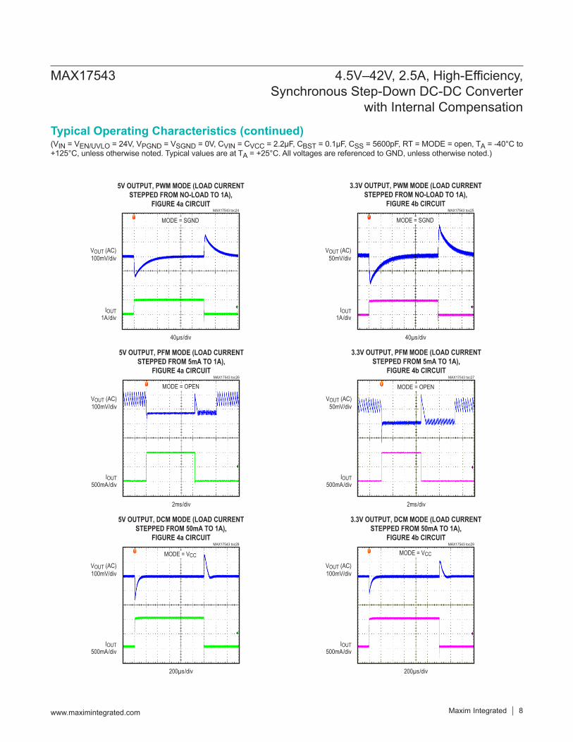
Typical Operating Characteristics (continued)
5V OUTPUT, PWM MODE (LOAD CURRENTSTEPPED FROM NO-LOAD TO 1A),
FIGURE 4a CIRCUITMAX17543 toc24
IOUT1A/div
VOUT (AC)100mV/div
40µs/div
MODE = SGND
5V OUTPUT, PFM MODE (LOAD CURRENTSTEPPED FROM 5mA TO 1A),
FIGURE 4a CIRCUITMAX17543 toc26
IOUT500mA/div
VOUT (AC)100mV/div
2ms/div
MODE = OPEN
5V OUTPUT, DCM MODE (LOAD CURRENTSTEPPED FROM 50mA TO 1A),
FIGURE 4a CIRCUITMAX17543 toc28
IOUT500mA/div
VOUT (AC)100mV/div
200µs/div
MODE = VCC
3.3V OUTPUT, PWM MODE (LOAD CURRENTSTEPPED FROM NO-LOAD TO 1A),
FIGURE 4b CIRCUITMAX17543 toc25
IOUT1A/div
VOUT (AC)50mV/div
40µs/div
MODE = SGND
3.3V OUTPUT, PFM MODE (LOAD CURRENTSTEPPED FROM 5mA TO 1A),
FIGURE 4b CIRCUITMAX17543 toc27
IOUT500mA/div
VOUT (AC)50mV/div
2ms/div
MODE = OPEN
3.3V OUTPUT, DCM MODE (LOAD CURRENTSTEPPED FROM 50mA TO 1A),
FIGURE 4b CIRCUITMAX17543 toc29
IOUT500mA/div
VOUT (AC)100mV/div
200µs/div
MODE = VCC
Maxim Integrated 8www.maximintegrated.com
MAX17543 4.5V–42V, 2.5A, High-Efficiency,Synchronous Step-Down DC-DC Converter
with Internal Compensation
(VIN = VEN/UVLO = 24V, VPGND = VSGND = 0V, CVIN = CVCC = 2.2µF, CBST = 0.1µF, CSS = 5600pF, RT = MODE = open, TA = -40°C to +125°C, unless otherwise noted. Typical values are at TA = +25°C. All voltages are referenced to GND, unless otherwise noted.)
Typical Operating Characteristics (continued)
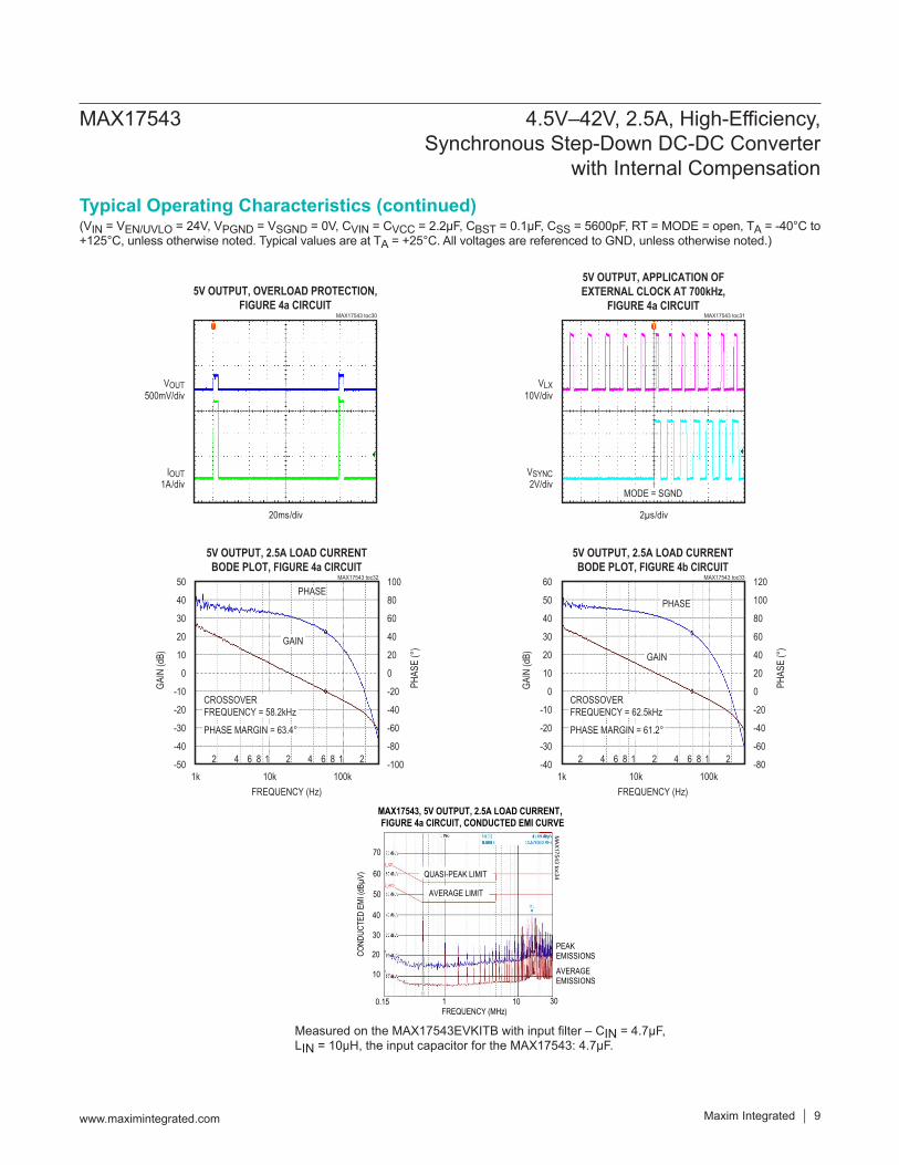
5V OUTPUT, OVERLOAD PROTECTION,FIGURE 4a CIRCUIT
MAX17543 toc30
IOUT1A/div
VOUT500mV/div
20ms/div
5V OUTPUT, 2.5A LOAD CURRENTBODE PLOT, FIGURE 4a CIRCUIT
FREQUENCY (Hz)
GAIN
(dB)
10k
-30
-20
-10
0
10
20
30
40
50
-40
-60
-40
-20
0
20
40
60
80
100
-80
1k2 4 6 8 1 2 4 6 8 1 2
100k
MAX17543 toc32
PHAS
E (°)
CROSSOVERFREQUENCY = 58.2kHz
PHASE MARGIN = 63.4°
GAIN
PHASE
-50 -100
MAX17543
toc34
MAX17543, 5V OUTPUT, 2.5A LOAD CURRENT,FIGURE 4a CIRCUIT, CONDUCTED EMI CURVE
0.15 1 10 30
AVERAGEEMISSIONS
PEAKEMISSIONSC
ON
DU
CTE
DEM
I(dB
µV)
FREQUENCY (MHz)
10
20
30
40
50
60
70
QUASI-PEAK LIMIT
AVERAGE LIMIT
5V OUTPUT, APPLICATION OFEXTERNAL CLOCK AT 700kHz,
FIGURE 4a CIRCUITMAX17543 toc31
VSYNC2V/div
VLX10V/div
2µs/div
MODE = SGND
5V OUTPUT, 2.5A LOAD CURRENTBODE PLOT, FIGURE 4b CIRCUIT
FREQUENCY (Hz)
GAIN
(dB)
10k
-30
-20
-10
0
10
20
30
40
50
-40
-60
-40
-20
0
20
40
60
80
100
-801k
2 4 6 8 1 2 4 6 8 1 2100k
MAX17543 toc33
PHAS
E (°)
CROSSOVERFREQUENCY = 62.5kHz
PHASE MARGIN = 61.2°
GAIN
PHASE
60 120
Measured on the MAX17543EVKITB with input filter – CIN = 4.7µF, LIN = 10µH, the input capacitor for the MAX17543: 4.7µF.
Maxim Integrated 9www.maximintegrated.com
MAX17543 4.5V–42V, 2.5A, High-Efficiency,Synchronous Step-Down DC-DC Converter
with Internal Compensation
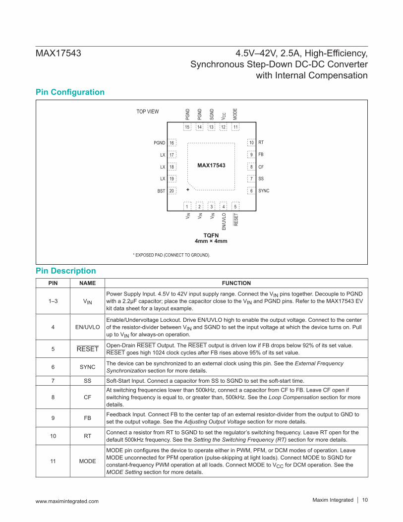
Pin Description
Pin Configuration
19
20
* EXPOSED PAD (CONNECT TO GROUND).
18
17
7
6
8
V IN
RESE
T
9
V IN
PGND
V CC
MODE
PGND
1 2
LX
4 5
15 14 12 11
LX
BST
FB
CF
SS
SYNC+
V IN
SGND
3
13
LX
16 10 RTPGND
TQFN4mm × 4mm
MAX17543
TOP VIEW
EN/U
VLO
PIN NAME FUNCTION
1–3 VIN
Power Supply Input. 4.5V to 42V input supply range. Connect the VIN pins together. Decouple to PGND with a 2.2µF capacitor; place the capacitor close to the VIN and PGND pins. Refer to the MAX17543 EV kit data sheet for a layout example.
4 EN/UVLOEnable/Undervoltage Lockout. Drive EN/UVLO high to enable the output voltage. Connect to the center of the resistor-divider between VIN and SGND to set the input voltage at which the device turns on. Pull up to VIN for always-on operation.
5 RESET Open-Drain RESET Output. The RESET output is driven low if FB drops below 92% of its set value. RESET goes high 1024 clock cycles after FB rises above 95% of its set value.
6 SYNC The device can be synchronized to an external clock using this pin. See the External Frequency Synchronization section for more details.
7 SS Soft-Start Input. Connect a capacitor from SS to SGND to set the soft-start time.
8 CFAt switching frequencies lower than 500kHz, connect a capacitor from CF to FB. Leave CF open if switching frequency is equal to, or greater than, 500kHz. See the Loop Compensation section for more details.
9 FB Feedback Input. Connect FB to the center tap of an external resistor-divider from the output to GND to set the output voltage. See the Adjusting Output Voltage section for more details.
10 RT Connect a resistor from RT to SGND to set the regulator’s switching frequency. Leave RT open for the default 500kHz frequency. See the Setting the Switching Frequency (RT) section for more details.
11 MODE
MODE pin configures the device to operate either in PWM, PFM, or DCM modes of operation. Leave MODE unconnected for PFM operation (pulse-skipping at light loads). Connect MODE to SGND for constant-frequency PWM operation at all loads. Connect MODE to VCC for DCM operation. See the MODE Setting section for more details.
MAX17543 4.5V–42V, 2.5A, High-Efficiency,Synchronous Step-Down DC-DC Converter
with Internal Compensation
www.maximintegrated.com Maxim Integrated 10
Pin Description (continued)PIN NAME FUNCTION12 VCC 5V LDO Output. Bypass VCC with 2.2µF ceramic capacitance to SGND.13 SGND Analog Ground
14–16 PGNDPower Ground. Connect the PGND pins externally to the power ground plane. Connect the SGND and PGND pins together at the ground return path of the VCC bypass capacitor. Refer to the MAX17543 EV kit data sheet for a layout example.
17–19 LX Switching Node. Connect LX pins to the switching-side of the inductor. Refer to the MAX17543 EV kit data sheet for a layout example.
20 BST Boost Flying Capacitor. Connect a 0.1µF ceramic capacitor between BST and LX.
— EPExposed Pad. Connect to the SGND pin. Connect to a large copper plane below the IC to improve heat dissipation capability. Add thermal vias below the exposed pad. Refer to the MAX17543 EV kit data sheet for a layout example.
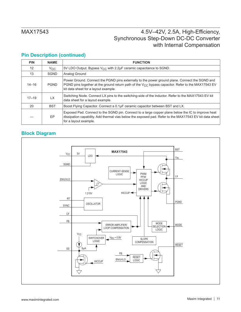
Block Diagram
VCC
SGND
1.215V
5V
LX
PGND
MODE
VIN
BST
LDO
EN/UVLO
RT
MAX17543
SYNC
CF
FB
SS
FB
OSCILLATOR
SWITCHOVERLOGIC
ERROR AMPLIFIER/LOOP COMPENSATION
MODESELECTION
LOGIC
SLOPECOMPENSATION
RESETLOGIC
CURRENT-SENSELOGIC
HICCUP
HICCUP
5µA
VCC
PWM/PFM/
HICCUPLOGICAND
DRIVERS
VBG = 0.9V
RESET
EN/UVLO
MAX17543 4.5V–42V, 2.5A, High-Efficiency,Synchronous Step-Down DC-DC Converter
with Internal Compensation
www.maximintegrated.com Maxim Integrated 11
Detailed DescriptionThe MAX17543 high-efficiency, high-voltage, synchro-nously-rectified step-down converter with dual integrated MOSFETs operates over a 4.5V to 42V input. It delivers up to 2.5A and 0.9V to 90%VIN output voltage. Built-in compensation across the output voltage range eliminates the need for external components. The feedback (FB) regulation accuracy over -40°C to +125°C is ±1.1%. The device features a peak-current-mode-control architecture. An internal transconductance error amplifier produces an integrated error voltage at an internal node, which sets the duty cycle using a PWM comparator, a high-side current-sense amplifier, and a slope-compensation generator. At each rising-edge of the clock, the high-side MOSFET turns on and remains on until either the appropriate or maximum duty cycle is reached, or the peak current limit is detected. During the high-side MOSFET’s on-time, the inductor current ramps up. During the second-half of the switching cycle, the high-side MOSFET turns off and the low-side MOSFET turns on. The inductor releases the stored energy as its current ramps down and provides current to the output. The device features a MODE pin that can be used to operate the device in PWM, PFM, or DCM control schemes. The device integrates adjustable-input undervoltage lockout, adjustable soft-start, open RESET, and external frequency-synchronization features.
Mode Selection (MODE)The logic state of the MODE pin is latched when VCC and EN/UVLO voltages exceed the respective UVLO rising thresholds and all internal voltages are ready to allow LX switching. If the MODE pin is open at power-up, the device operates in PFM mode at light loads. If the MODE pin is grounded at power-up, the device operates in constant-frequency PWM mode at all loads. Finally, if the MODE pin is connected to VCC at power-up, the device operates in constant-frequency DCM mode at light loads. State changes on the MODE pin are ignored during normal operation.
PWM Mode OperationIn PWM mode, the inductor current is allowed to go negative. PWM operation provides constant frequency operation at all loads, and is useful in applications sensitive to switching frequency. However, the PWM mode of operation gives lower efficiency at light loads when compared to PFM and DCM modes of operation.
PFM Mode OperationThe PFM mode of operation disables negative inductor current and also skips pulses at light loads for high efficiency. In PFM mode, the inductor current is forced to a fixed peak of 750mA every clock cycle until the output rises to 102.3% of the nominal voltage. Once the output reaches 102.3% of the nominal voltage, both the high-side and low-side FETs are turned off and the device enters hibernation mode until the load discharges the output to 101.1% of the nominal voltage. Most of the internal blocks are turned off in hibernation mode to save quiescent current. After the output falls below 101.1% of the nominal voltage, the device comes out of hibernation mode, turns on all internal blocks, and again commences the process of delivering pulses of energy to the output until it reaches 102.3% of the nominal output voltage.The advantage of PFM mode is higher efficiency at light loads due to lower quiescent current drawn from sup-ply. The disadvantage is that the output voltage ripple is higher than in the PWM or DCM modes of operation, and the switching frequency is not constant at light loads.
DCM Mode OperationThe DCM mode of operation features constant-frequency operation down to lighter loads than PFM mode by disabling negative inductor current at light loads instead of skipping pulses. DCM operation offers efficiency performance that lies between the PWM and PFM modes.
Linear Regulator (VCC)An internal linear regulator (VCC) provides a 5V nominal supply to power the internal blocks and the low-side MOSFET driver. The output of the linear regulator (VCC) should be bypassed with a 2.2µF ceramic capacitor to SGND. The device employs an undervoltage lockout circuit that disables the internal linear regulator when VCC falls below 3.8V (typ).
Setting the Switching Frequency (RT)The switching frequency of the device can be programmed from 100kHz to 2.2MHz by using a resistor connected from the RT pin to SGND. The switching frequency (fSW) is related to the resistor connected at the RT pin (RRT) by the following equation:
3RT
SW
21 10R 1.7f×
≅ −
where RRT is in kΩ and fSW is in kHz. Leaving the RT pin open causes the device to operate at the default switching frequency of 500kHz. See Table 1 for RT resistor values for a few common switching frequencies. To operate the MAX17543 at switching frequencies lower than 200kHz, an
MAX17543 4.5V–42V, 2.5A, High-Efficiency,Synchronous Step-Down DC-DC Converter
with Internal Compensation
www.maximintegrated.com Maxim Integrated 12
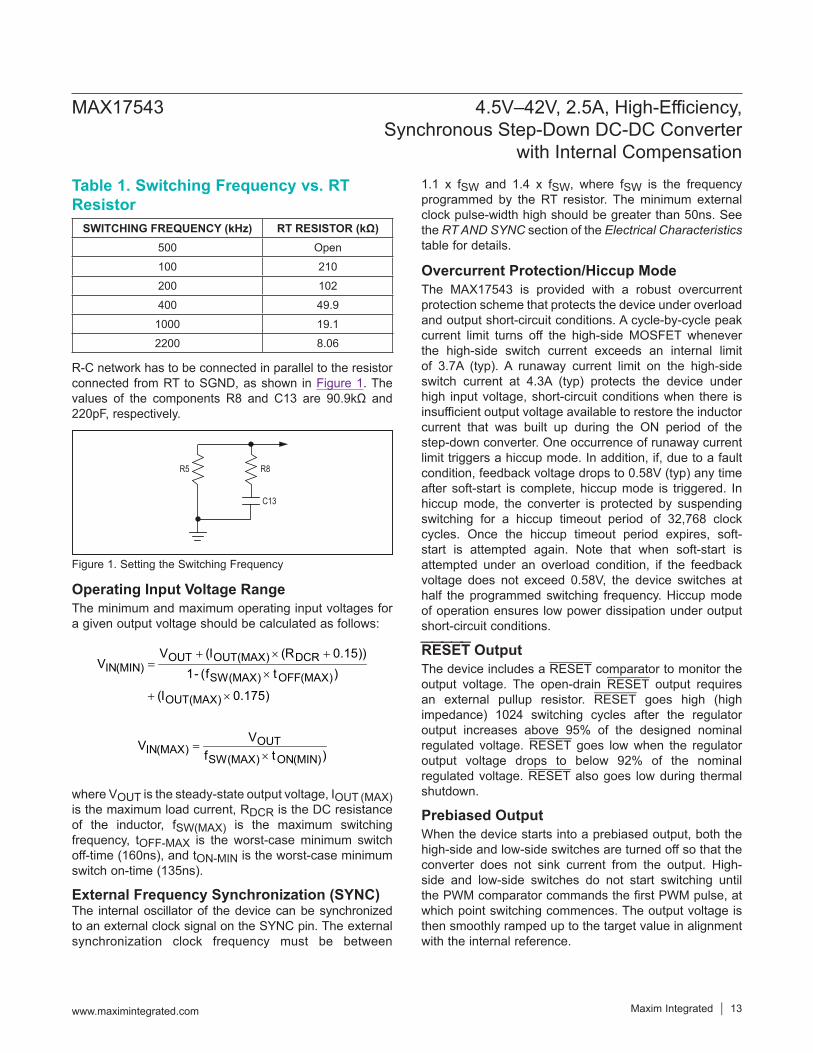
R-C network has to be connected in parallel to the resistor connected from RT to SGND, as shown in Figure 1. The values of the components R8 and C13 are 90.9kΩ and 220pF, respectively.
Operating Input Voltage RangeThe minimum and maximum operating input voltages for a given output voltage should be calculated as follows:
OUT OUT(MAX) DCRIN(MIN)
SW(MAX) OFF(MAX)
OUT(MAX)
V (I (R 0.15))V
1- (f t )
(I 0.175)
+ × +=
×
+ ×
OUTIN(MAX)
SW(MAX) ON(MIN)
VVf t )
=×
where VOUT is the steady-state output voltage, IOUT (MAX) is the maximum load current, RDCR is the DC resistance of the inductor, fSW(MAX) is the maximum switching frequency, tOFF-MAX is the worst-case minimum switch off-time (160ns), and tON-MIN is the worst-case minimum switch on-time (135ns).
External Frequency Synchronization (SYNC)The internal oscillator of the device can be synchronized to an external clock signal on the SYNC pin. The external synchronization clock frequency must be between
1.1 x fSW and 1.4 x fSW, where fSW is the frequency programmed by the RT resistor. The minimum external clock pulse-width high should be greater than 50ns. See the RT AND SYNC section of the Electrical Characteristics table for details.
Overcurrent Protection/Hiccup ModeThe MAX17543 is provided with a robust overcurrent protection scheme that protects the device under overload and output short-circuit conditions. A cycle-by-cycle peak current limit turns off the high-side MOSFET whenever the high-side switch current exceeds an internal limit of 3.7A (typ). A runaway current limit on the high-side switch current at 4.3A (typ) protects the device under high input voltage, short-circuit conditions when there is insufficient output voltage available to restore the inductor current that was built up during the ON period of the step-down converter. One occurrence of runaway current limit triggers a hiccup mode. In addition, if, due to a fault condition, feedback voltage drops to 0.58V (typ) any time after soft-start is complete, hiccup mode is triggered. In hiccup mode, the converter is protected by suspending switching for a hiccup timeout period of 32,768 clock cycles. Once the hiccup timeout period expires, soft-start is attempted again. Note that when soft-start is attempted under an overload condition, if the feedback voltage does not exceed 0.58V, the device switches at half the programmed switching frequency. Hiccup mode of operation ensures low power dissipation under output short-circuit conditions.
RESET OutputThe device includes a RESET comparator to monitor the output voltage. The open-drain RESET output requires an external pullup resistor. RESET goes high (high impedance) 1024 switching cycles after the regulator output increases above 95% of the designed nominal regulated voltage. RESET goes low when the regulator output voltage drops to below 92% of the nominal regulated voltage. RESET also goes low during thermal shutdown.
Prebiased OutputWhen the device starts into a prebiased output, both the high-side and low-side switches are turned off so that the converter does not sink current from the output. High-side and low-side switches do not start switching until the PWM comparator commands the first PWM pulse, at which point switching commences. The output voltage is then smoothly ramped up to the target value in alignment with the internal reference.
Table 1. Switching Frequency vs. RT Resistor
Figure 1. Setting the Switching Frequency
R5 R8
C13
SWITCHING FREQUENCY (kHz) RT RESISTOR (kΩ)500 Open100 210200 102400 49.9
1000 19.12200 8.06
MAX17543 4.5V–42V, 2.5A, High-Efficiency,Synchronous Step-Down DC-DC Converter
with Internal Compensation
www.maximintegrated.com Maxim Integrated 13
Thermal-Shutdown ProtectionThermal-shutdown protection limits total power dissipation in the device. When the junction temperature of the device exceeds +165ºC, an on-chip thermal sensor shuts down the device, allowing it to cool. The thermal sensor turns the device on again after the junction temperature cools by 10ºC. Soft-start resets during thermal shutdown. Carefully evaluate the total power dissipation (see the Power Dissipation section) to avoid unwanted triggering of the thermal shutdown in normal operation.
Applications InformationInput Capacitor SelectionThe input filter capacitor reduces peak currents drawn from the power source and reduces noise and voltage ripple on the input caused by the circuit’s switching. The input capacitor RMS current requirement (IRMS) is defined by the following equation:
×= × OUT IN OUT
RMS OUT(MAX)IN
V (V - V )I I
V
where, IOUT(MAX) is the maximum load current. IRMS has a maximum value when the input voltage equals twice the output voltage (VIN = 2 x VOUT), so IRMS(MAX) = IOUT(MAX)/2.Choose an input capacitor that exhibits less than +10ºC temperature rise at the RMS input current for optimal long-term reliability. Use low-ESR ceramic capacitors with high-ripple-current capability at the input. X7R capacitors are recommended in industrial applications for their temperature stability. Calculate the input capacitance using the following equation:
× ×=
η× × ∆OUT(MAX)
INSW IN
I D (1- D)C
f V
where D = VOUT/VIN is the duty ratio of the controller, fSW is the switching frequency, ΔVIN is the allowable input voltage ripple, and η is the efficiency.In applications where the source is located some distance from the device input, an electrolytic capacitor should be added in parallel to the ceramic capacitor to provide necessary damping for potential oscillations caused by the inductance of the longer input power path and input ceramic capacitor.
Inductor SelectionThree key inductor parameters must be specified for operation with the device: inductance value (L), inductor
saturation current (ISAT), and DC resistance (RDCR). The switching frequency and output voltage determine the inductor value as follows:
OUTSW
VLf
=
where VOUT, and fSW are nominal values. Select a low-loss inductor closest to the calculated value with acceptable dimensions and having the lowest possible DC resistance. The saturation current rating (ISAT) of the inductor must be high enough to ensure that saturation can occur only above the peak current-limit value of 3.7A.
Output Capacitor SelectionX7R ceramic output capacitors are preferred due to their stability over temperature in industrial applications. The output capacitors are usually sized to support a step load of 50% of the maximum output current in the application, such that output voltage deviation is contained to 3% of nominal output voltage. The minimum required output capacitance can be calculated as follows:
( )OUTC OUT
5.5Cf V
=×
where COUT is in Farad and fC is the target closed-loop crossover frequency in Hz. Select fC to be 1/9th of fSW if the switching frequency is less than or equal to 500kHz. If the switching frequency is more than 500kHz, select fC to be 55kHz.Derating of ceramic capacitors with DC-voltage must be considered while selecting the output capacitor. Derating curves are available from all major ceramic capacitor vendors.
Soft-Start Capacitor SelectionThe device implements adjustable soft-start operation to reduce inrush current. A capacitor connected from the SS pin to SGND programs the soft-start time. The selected output capacitance (CSEL) and the output voltage (VOUT) determine the minimum required soft-start capacitor as follows:
-6SS SEL OUTC 28 10 C V≥ × × ×
The soft-start time (tSS) is related to the capacitor connected at SS (CSS) by the following equation:
SSSS -6
Ct5.55 10
=×
For example, to program a 1ms soft-start time, a 5.6nF capacitor should be connected from the SS pin to SGND.
MAX17543 4.5V–42V, 2.5A, High-Efficiency,Synchronous Step-Down DC-DC Converter
with Internal Compensation
www.maximintegrated.com Maxim Integrated 14
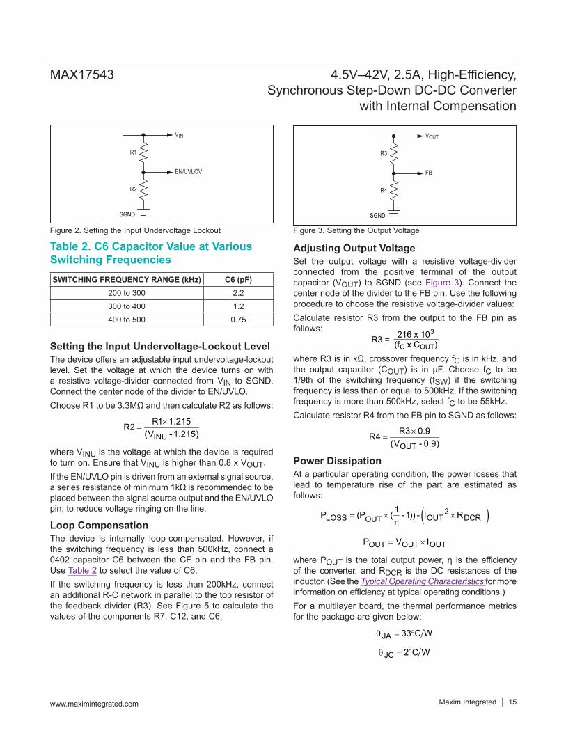
Setting the Input Undervoltage-Lockout LevelThe device offers an adjustable input undervoltage-lockout level. Set the voltage at which the device turns on with a resistive voltage-divider connected from VIN to SGND. Connect the center node of the divider to EN/UVLO.Choose R1 to be 3.3MΩ and then calculate R2 as follows:
×=
INU
R1 1.215R2(V -1.215)
where VINU is the voltage at which the device is required to turn on. Ensure that VINU is higher than 0.8 x VOUT.If the EN/UVLO pin is driven from an external signal source, a series resistance of minimum 1kΩ is recommended to be placed between the signal source output and the EN/UVLO pin, to reduce voltage ringing on the line.
Loop CompensationThe device is internally loop-compensated. However, if the switching frequency is less than 500kHz, connect a 0402 capacitor C6 between the CF pin and the FB pin. Use Table 2 to select the value of C6.If the switching frequency is less than 200kHz, connect an additional R-C network in parallel to the top resistor of the feedback divider (R3). See Figure 5 to calculate the values of the components R7, C12, and C6.
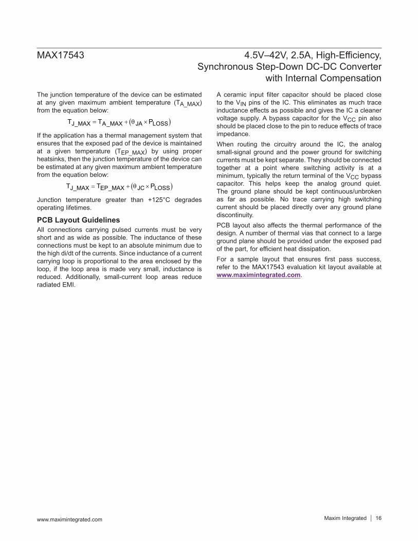
Adjusting Output VoltageSet the output voltage with a resistive voltage-divider connected from the positive terminal of the output capacitor (VOUT) to SGND (see Figure 3). Connect the center node of the divider to the FB pin. Use the following procedure to choose the resistive voltage-divider values:Calculate resistor R3 from the output to the FB pin as follows:
216 x 103
(fC x COUT)R3 =
where R3 is in kΩ, crossover frequency fC is in kHz, and the output capacitor (COUT) is in μF. Choose fC to be 1/9th of the switching frequency (fSW) if the switching frequency is less than or equal to 500kHz. If the switching frequency is more than 500kHz, select fC to be 55kHz.Calculate resistor R4 from the FB pin to SGND as follows:
×=
OUT
R3 0.9R4(V - 0.9)
Power DissipationAt a particular operating condition, the power losses that lead to temperature rise of the part are estimated as follows:
( )= × ×η
2LOSS OUT DCROUT
1P (P ( -1)) - I R
= ×OUT OUT OUTP V I
where POUT is the total output power, η is the efficiency of the converter, and RDCR is the DC resistances of the inductor. (See the Typical Operating Characteristics for more information on efficiency at typical operating conditions.)For a multilayer board, the thermal performance metrics for the package are given below:
JA 33 C Wθ = °
JC 2 C Wθ = °
Figure 2. Setting the Input Undervoltage Lockout Figure 3. Setting the Output Voltage
Table 2. C6 Capacitor Value at Various Switching FrequenciesSWITCHING FREQUENCY RANGE (kHz) C6 (pF)
200 to 300 2.2300 to 400 1.2400 to 500 0.75
SGND
R3
VOUT
R4
FB
SGND
R1
VIN
R2
EN/UVLOV
MAX17543 4.5V–42V, 2.5A, High-Efficiency,Synchronous Step-Down DC-DC Converter
with Internal Compensation
www.maximintegrated.com Maxim Integrated 15
The junction temperature of the device can be estimated at any given maximum ambient temperature (TA_MAX) from the equation below:
( )= + θ ×J_MAX A_MAX JA LOSST T P
If the application has a thermal management system that ensures that the exposed pad of the device is maintained at a given temperature (TEP_MAX) by using proper heatsinks, then the junction temperature of the device can be estimated at any given maximum ambient temperature from the equation below:
( )= + θ ×J_MAX EP_MAX JC LOSST T P
Junction temperature greater than +125°C degrades operating lifetimes.
PCB Layout GuidelinesAll connections carrying pulsed currents must be very short and as wide as possible. The inductance of these connections must be kept to an absolute minimum due to the high di/dt of the currents. Since inductance of a current carrying loop is proportional to the area enclosed by the loop, if the loop area is made very small, inductance is reduced. Additionally, small-current loop areas reduce radiated EMI.
A ceramic input filter capacitor should be placed close to the VIN pins of the IC. This eliminates as much trace inductance effects as possible and gives the IC a cleaner voltage supply. A bypass capacitor for the VCC pin also should be placed close to the pin to reduce effects of trace impedance. When routing the circuitry around the IC, the analog small-signal ground and the power ground for switching currents must be kept separate. They should be connected together at a point where switching activity is at a minimum, typically the return terminal of the VCC bypass capacitor. This helps keep the analog ground quiet. The ground plane should be kept continuous/unbroken as far as possible. No trace carrying high switching current should be placed directly over any ground plane discontinuity.PCB layout also affects the thermal performance of the design. A number of thermal vias that connect to a large ground plane should be provided under the exposed pad of the part, for efficient heat dissipation.For a sample layout that ensures first pass success, refer to the MAX17543 evaluation kit layout available at www.maximintegrated.com.
MAX17543 4.5V–42V, 2.5A, High-Efficiency,Synchronous Step-Down DC-DC Converter
with Internal Compensation
www.maximintegrated.com Maxim Integrated 16
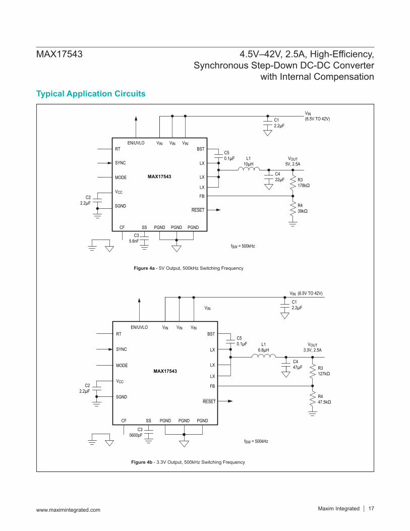
Typical Application Circuits
RESET
VIN VIN VINBSTRT
SYNC
MODE
VCC
SGND
CF SS
FB
PGNDPGNDPGND
LX
LX
LX
EN/UVLO
MAX17543
L110µH
C50.1µF
C422µF R3
178kΩ
R439kΩ
VOUT5V, 2.5A
VIN(6.5V TO 42V)C1
2.2µF
C35.6nF
fSW = 500kHz
Figure 4a - 5V Output, 500kHz Switching Frequency
Figure 4b - 3.3V Output, 500kHz Switching Frequency
RESET
VIN VIN VINBSTRT
SYNC
MODE
VCC
SGND
CF SS
FB
PGNDPGNDPGND
LX
LX
LX
VIN (6.5V TO 42V)
EN/UVLO
MAX17543
L16.8µH
C50.1µF
C447µF R3
127kΩ
R447.5kΩ
VOUT3.3V, 2.5A
C12.2µF
C35600pF
C22.2µF
fSW = 500kHz
VIN
C22.2µF
MAX17543 4.5V–42V, 2.5A, High-Efficiency,Synchronous Step-Down DC-DC Converter
with Internal Compensation
www.maximintegrated.com Maxim Integrated 17
Note: All devices operate over the -40ºC to +125ºC tempera-ture range, unless otherwise noted.+Denotes a lead(Pb)-free/RoHS-compliant package. *EP = Exposed pad.
*EP = Exposed pad.
Package InformationFor the latest package outline information and land patterns (footprints), go to www.maximintegrated.com/packages. Note that a “+”, “#”, or “-” in the package code indicates RoHS status only. Package drawings may show a different suffix character, but the drawing pertains to the package regardless of RoHS status.
Chip InformationPROCESS: BiCMOS
Ordering Information
Typical Application Circuits (continued)
PART PIN-PACKAGEMAX17543ATP+ 20 TQFN 4mm x 4 mm
PACKAGE TYPE
PACKAGE CODE
OUTLINENO.
LAND PATTERN NO.
20 TQFN-EP T2044+4 21-0139 90-0409
Figure 5 - 3.3V Output, 100kHz Switching Frequency
CF
VIN VIN VINBSTRT
R890.9kΩ
C13220pF
R5210kΩ
SYNC
MODE
VCC
SGND
RESETB SS
FB
PGNDPGNDPGND
LX
LX
LX
EN/UVLO
MAX17543
L133µH
C50.1µF
C615pF
R397.6kΩ R7
1kΩ
C4100µF
R436.5kΩ
VOUT3.3V, 2.5A
VIN(4.5V to 42V)
C12.2µF
C333000pF
C4 = C9 = C14 = JMK325ABJ107MM-T
C22.2µF
fSW = 100kHzC12 = 0.5/ (R3 x fSW)R7 = R3/100C6 = (1.4 x 10⁻⁶)/fSW
C82.2µF
C14100µF
C9100µF
C1247pF
MAX17543 4.5V–42V, 2.5A, High-Efficiency,Synchronous Step-Down DC-DC Converter
with Internal Compensation
www.maximintegrated.com Maxim Integrated 18
Revision HistoryREVISIONNUMBER
REVISIONDATE DESCRIPTION PAGES
CHANGED0 9/14 Initial release —1 7/16 Updated operating and junction temperature values, added new TOC and text 1–9, 15, 16
1.1 Corrected typo in the Applications Information section 14
Maxim Integrated cannot assume responsibility for use of any circuitry other than circuitry entirely embodied in a Maxim Integrated product. No circuit patent licenses are implied. Maxim Integrated reserves the right to change the circuitry and specifications without notice at any time. The parametric values (min and max limits) shown in the Electrical Characteristics table are guaranteed. Other parametric values quoted in this data sheet are provided for guidance.
Maxim Integrated and the Maxim Integrated logo are trademarks of Maxim Integrated Products, Inc. © 2016 Maxim Integrated Products, Inc. 19
MAX17543 4.5V–42V, 2.5A, High-Efficiency,Synchronous Step-Down DC-DC Converter
with Internal Compensation
For pricing, delivery, and ordering information, please contact Maxim Direct at 1-888-629-4642, or visit Maxim Integrated’s website at www.maximintegrated.com.
Related Documents