Evaluates: MAX11270 MAX1127X Family Evaluation Kit General Description The evaluation kit (EV kit) demonstrates the MAX1127X family of 24-bit, 64ksps delta-sigma ADCs with integrated PGA. The EV kit includes a graphical user interface (GUI) that provides communication from the target device to the PC. The EV kit can operate in multiple modes: 1) Standalone Mode: In “Standalone” mode, the EV kit is connected to the PC through a USB cable and performs a subset of the complete EV kit functions with limitation for sample rate and size. 2) FPGA Mode: In “FPGA” mode, the EV kit is con- nected to an Avnet ZedBoard™ through a low-pin- count FMC connector. ZedBoard features a Xilinx ® Zynq ® -7000 SoC that connects to the PC through an Ethernet port, which allows the GUI to perform differ- ent operations with full control over mezzanine card functions. The EV kit with FPGA platform performs the complete suite of evaluation tests for the target IC 3) User-Supplied SPI Mode: In addition to the USB and FMC interfaces, the EV kit provides two 12-pin PMOD-style headers for user-supplied SPI interface, to connect the signals for RDYB, SCLK, DIN, DOUT, and CSB. The EV kit includes Windows XP ® -, Windows ® 7 and Windows 8.1-compatible software to exercise the features of the IC. The EV kit GUI allows different sample sizes, adjustable sampling rates, on-board or external reference options, and graphing software that includes the FFT and histogram of the sampled signals with the ability to save plots in .jpg or .csv formats. The ZedBoard board accepts a +12V AC-DC wall adapter. The EV kit can be powered by the ZedBoard or by a local 12V supply. The EV kit has on-board transformers and digital isolators to separate the IC from the ZedBoard/ on-board processor. The MAX11270 EV kit comes installed with a MAX11270EUG+ in a 24-pin TSSOP package. Features and Benefits ● High-Speed USB, FMC Connector, and PMOD Connector ● 5MHz SPI Interface ● Various Sample Sizes and Sample Rates ● Collects Up to 1 Million Samples (with FPGA Platform) ● Time Domain, Frequency Domain, and Histogram Plotting ● Save Plots as jpg, bmp or csv ● Sync In and Sync Out for Coherent Sampling (with FPGA Platform) ● On-Board DAC (MAX542) for DC Signal-Level Generation ● On-Board Voltage Reference (MAX6126) ● Proven PCB Layout ● Fully Assembled and Tested ● Windows XP-, Windows 7-, and Windows 8.1-Compatible Software ● Savable ADC Configurations 19-7592; Rev 0; 4/15 Ordering Information appears at end of data sheet. ZedBoard is a trademark of Avnet, Inc. Xilinx and Zynq are registered trademarks and Xilinx is a regis- tered service mark of Xilinx, Inc. Windows and Windows XP are registered trademarks and reg- istered service marks of Microsoft Corporation.

Welcome message from author
This document is posted to help you gain knowledge. Please leave a comment to let me know what you think about it! Share it to your friends and learn new things together.
Transcript
Evaluates: MAX11270MAX1127X Family Evaluation Kit
General DescriptionThe evaluation kit (EV kit) demonstrates the MAX1127X family of 24-bit, 64ksps delta-sigma ADCs with integrated PGA. The EV kit includes a graphical user interface (GUI) that provides communication from the target device to the PC. The EV kit can operate in multiple modes:1) Standalone Mode: In “Standalone” mode, the EV
kit is connected to the PC through a USB cable and performs a subset of the complete EV kit functions with limitation for sample rate and size.
2) FPGA Mode: In “FPGA” mode, the EV kit is con-nected to an Avnet ZedBoard™ through a low-pin-count FMC connector. ZedBoard features a Xilinx® Zynq®-7000 SoC that connects to the PC through an Ethernet port, which allows the GUI to perform differ-ent operations with full control over mezzanine card functions. The EV kit with FPGA platform performs the complete suite of evaluation tests for the target IC
3) User-Supplied SPI Mode: In addition to the USB and FMC interfaces, the EV kit provides two 12-pin PMOD-style headers for user-supplied SPI interface, to connect the signals for RDYB, SCLK, DIN, DOUT, and CSB.
The EV kit includes Windows XP®-, Windows® 7 and Windows 8.1-compatible software to exercise the features of the IC. The EV kit GUI allows different sample sizes, adjustable sampling rates, on-board or external reference options, and graphing software that includes the FFT and histogram of the sampled signals with the ability to save plots in .jpg or .csv formats. The ZedBoard board accepts a +12V AC-DC wall adapter. The EV kit can be powered by the ZedBoard or by a local 12V supply. The EV kit has on-board transformers and digital isolators to separate the IC from the ZedBoard/on-board processor. The MAX11270 EV kit comes installed with a MAX11270EUG+ in a 24-pin TSSOP package.
Features and Benefits ● High-Speed USB, FMC Connector, and PMOD
Connector ● 5MHz SPI Interface ● Various Sample Sizes and Sample Rates ● Collects Up to 1 Million Samples (with FPGA Platform) ● Time Domain, Frequency Domain, and Histogram
Plotting ● Save Plots as jpg, bmp or csv ● Sync In and Sync Out for Coherent Sampling
(with FPGA Platform) ● On-Board DAC (MAX542) for DC Signal-Level
Generation ● On-Board Voltage Reference (MAX6126) ● Proven PCB Layout ● Fully Assembled and Tested ● Windows XP-, Windows 7-, and Windows
8.1-Compatible Software ● Savable ADC Configurations
19-7592; Rev 0; 4/15
Ordering Information appears at end of data sheet.
ZedBoard is a trademark of Avnet, Inc.Xilinx and Zynq are registered trademarks and Xilinx is a regis-tered service mark of Xilinx, Inc.Windows and Windows XP are registered trademarks and reg-istered service marks of Microsoft Corporation.

Maxim Integrated │ 2www.maximintegrated.com
Evaluates: MAX11270MAX1127X Family Evaluation Kit
-+
MAX44241-+
MAX44241MAX11270
ADCU25
-+
MAX44241-+
MAX44241
SCLK_ADCCS_ADC
DIN_ADCDOUT_ADC
ISOLATION
MAX542DACU15
CS_DAC
DIN_DACLDAC
FMC
HEADER
USB
FTDI
FPGA - ZedBoard
USER-SUPPLIED SPI
PC - USB
SYNC IN, SYNC OUT
ISOLATED DC-DC
MAX6126
MAX6126
EXT_REFPADC_REFP
ADC_REFN
EXT_REFN
ADC_REFPDAC_OUT+
ADC_INP
ADC_INN
ADC_REFNDAC_OUT-
SCLK_DAC
-+
MAX9632
DAC_OUT+
DAC_OUT-
MAX9632 x2
RDYB_ADC
MAX11270 EV Kit Photo
System Block Diagram

Maxim Integrated │ 3www.maximintegrated.com
Evaluates: MAX11270MAX1127X Family Evaluation Kit
Quick StartRequired Equipment
● MAX11270 EV kit ● +12V (500mA) power supply ● Micro-USB cable ● ZedBoard development board (optional – Not Included
with EV kit) ● Function generator (optional) ● Windows XP, Windows 7, or Windows 8.1 PC with a
spare USB portNote: In the following sections, software-related items are identified by bolding. Text in bold refers to items directly from the EV system software. Text in bold and underline refers to items from the Windows operating system.
ProcedureThe EV kit is fully assembled and tested. Follow the steps below to verify board operation:1) Visit www.maximintegrated.com/evkitsoftware to
download the latest version of the EV kit software, MAX11270EVK.ZIP. Save the EV kit software to a temporary folder and uncompress the ZIP file.
2) Install the EV kit software and USB driver on your com-puter by running the MAX11270EVKitSetupV1.1.exe program inside the temporary folder. The program files are copied to your PC and icons are created in the Windows Start | Programs menu. At the end of the installation process, the installer will launch the installer for the FTDIChip CDM drivers.For Standalone mode:
3) Verify that all jumpers are in their default positions for the EV kit (Table 2).
4) Connect the PC to the EV kit using a micro-USB cable.
5) Connect the +12V adapter to the EV kit.6) Start the EV kit software by opening its icon in the
Start | Programs menu. The EV kit software appears as shown in Figure 1. Verify that the lower left status bar indicates the EV kit hardware is Connected.
7) From the Device menu, select Standalone and click Search for USB Device. Then select Standalone again and select a device in the list. Verify that the lower left status bar indicates the EV kit hardware is Connected.For FPGA mode (when connected to a ZedBoard):
8) Connect the Ethernet cable from the PC to the ZedBoard and configure the Internet Protocol Version 4 (TCP/Ipv4) properties in the local area connec-tion to IP address 192.168.1.2 and subnet Mask to 255.255.255.0.
9) Verify that the ZedBoard SD card contains the boot.bin file for the MAX11270 EV kit.
10) Connect the EV kit FMC connector to the ZedBoard FMC connector. Gently press them together.
11) Verify that all jumpers are in their default positions for the ZedBoard (Table 1) and EV kit (Table 2).
12) Connect the 12V wall adapter power supply to the ZedBoard. Leave the ZedBoard powered off. Connect the PC to the ZedBoard with an Ethernet cable.
13) Enable the power supply by sliding SW8 to ON. 14) Start the EV kit software by opening its icon in the
Start | Programs menu. The EV kit software appears as shown in Figure 1. From the Device menu, select FPGA. Verify that the lower left status bar indicates the EV kit hardware is Connected. For either Standalone or FPGA mode:
15) Connect the positive terminal of the function generator to the IN+ test point on the EV kit. Connect the nega-tive terminal of the function generator to the IN- test point on the EV kit. Disable the function generator.
16) Enable the function generator. Configure the signal source to generate a 1kHz, 1VP-P sinusoidal wave with +500mV offset.
17) In the Calibration group, select Self Offset/Gain in the drop-down list and then click Calibrate.
18) Click on the Scope tab. 19) Check the Remove DC checkbox to remove the DC
component of the sampled data.20) Click the Capture button to read sampled data from
the ADC. 21) The EV kit software appears as shown in Figure 4. 22) Verify the frequency is approximately 1kHz displayed
on the right. The scope graph has buttons in the upper-right corner that allow zooming in to detail.
FILE DECRIPTION
MAX11270EVKitSetupV1.1.exe Application Program (GUI)
Boot.bin ZedBoard Firmware (SD Card to boot Zynq)
MAX11270 EV Kit Files

Maxim Integrated │ 4www.maximintegrated.com
Evaluates: MAX11270MAX1127X Family Evaluation Kit
Table 1. ZedBoard Jumper Settings (Optional)
Table 2. MAX1127X EV Kit User Configuration Jumper Settings*
JUMPER SHUNT POSITION DESCRIPTION
J18 1-2 VDDIO set for 3.3VJP11 2-3
Boot from SD card
JP10 1-2JP9 1-2JP8 2-3JP7 2-3
JP10 —J12 — SD card installedJ20 — Connected to 12V wall adapterSW8 Off ZedBoard power switch, off while connecting boards
JUMPER SHUNT POSITION DESCRIPTION
J2 (Red)1-2 Connects the +10V rail to test point +10VEXT for external power (op amp + supply)2-3* Connects the +10V rail to LDO U2 (op amp + supply)
J3 (Red)1-2 Connects the +15V rail to test point +15EXT for external power (powers U2)2-3* Connects the +15V rail to isolation transformer (powers U2)
J4 (Red)1-2 Set ADC DVDD to +3.3V2-3* Set ADC DVDD to +2.0V
J5 (Red)1-2* Connect ADC AVSS to GND (unipolar mode – also set J8 for unipolar)2-3 Connect ADC AVSS to -1.8V (bipolar mode – also set J8 for bipolar)
J6 (Black)1-2 Apply an offset of ADC_REFP (2.5V default) to amplifier U242-3 Apply an offset of 2.5V to amplifier U24
Open* No offset for amplifier U24
J7 (Black)1-2 Apply an offset of ADC_REFP (2.5V default) to amplifier U272-3 Apply an offset of 2.5V to amplifier U27
Open* No offset for amplifier U27
J8 (Red)1-2 Connect ADC AVDD to +1.8V (bipolar mode)2-3* Connect ADC AVDD to 3.6V (unipolar mode)
J15 (Red)1-2* Connects ZedBoard +12V to main power supply (U3). Diode D2 protects supplies.
Open Disconnects ZedBoard +12V from main power supply
J17 (Red)1-2 Connects U5 input to GND3-4 Connects U5 input to test point -15VEXT for external power5-6* Connects U5 input to isolation transformer
J18 (Red)1-2 Do not connect3-4 Do not connect5-6 Connects U5 output to GND, which sets the reference for the -10V supply (op amp - supply)
J20 (Red)1-2* Connects on-board FTDI chip to 3.3V, necessary for standalone mode
Open Disconnects on-board FTDI chip power. This jumper does not interfere with the ZedBoard.
J21 (Black)1-2* Drive ADC REFP pin with on-board voltage reference2-3 Drive ADC REFP pin with external voltage reference

Maxim Integrated │ 5www.maximintegrated.com
Evaluates: MAX11270MAX1127X Family Evaluation Kit
Table 2. MAX1127X EV Kit User Configuration Jumper Settings* (continued)
JUMPER SHUNT POSITION DESCRIPTION
J22 (Black)1-2 Ground test point CH_D- 3-4 Ground test point CH_D+
J23 (Black)1-2* Drive ADC REFN pin with on-board voltage reference2-3 Drive ADC REFN pin with external voltage reference
J24 (Black)1-2 Ground test point CH_C- 3-4 Ground test point CH_C+
J25 (Black)
1-2* Connect output of U23 (CH_C) to U24 inverting input3-4 Connect CH_D- to U24 inverting input5-6 Connect output of U23 (CH_C) to U24 noninverting input7-8 Connect CH_D+ to U24 noninverting input
J26, J27 (Black)
1-2* Set both jumpers to align with silkscreen text “EXT” to drive ADC_INP and ADC_INN with test points IN+ and IN- (also external connector J10 is on same net)
3-4 Set both jumpers to align with silkscreen text “AMP” to drive ADC_INP and ADC_INN with U27 and U24 amplifiers
5-6 Set both jumpers to align with silkscreen text “DAC” to drive ADC_INP and ADC_INN with DAC_OUT+ and DAC_OUT-
7-8 Set both jumpers to align with silkscreen text “REF” to drive ADC_INP and ADC_INN with ADC_REFP and ADC_REFN voltage reference
9-10 Ground ADC_INP and INN
J28 (Black)1-2 Ground test point CH_A- 3-4 Ground test point CH_A+
J29 (Black)
1-2* Connect output of U26 (CH_A) to U27 inverting input3-4 Connect CH_B- to U27 inverting input5-6 Connect output of U26 (CH_A) to U27 noninverting input7-8 Connect CH_B+ to U27 noninverting input
J30 (Black)1-2 Ground test point CH_B- 3-4 Ground test point CH_B+
J36 (Black)1-2 Drive ADC CLK pin with signal from SMA connector J342-3* Drive ADC CLK pin with signal from on-board oscillator U20
J37 (Red)1-2* Connect ADC to the DVDD voltage selection jumper J4open Attach amp meter between pins 1-2 to measure current consumed by ADC DVDD
J40 (Black)1-2* Connect ADC RST to DVDD (normal operation)2-3 Connect ADC RST to GND (reset state)
J44 (Black)1-2* Sets U18 noninverting input to 0V. Gain = -1 with offset = 0. Drives DAC_OUT-.2-3 Sets U18 noninverting input to 2.5V. Gain = -1 with offset = 2.5V. Drives DAC_OUT-.
J45 (Black)1-2* Sets U17 noninverting input to 0V. Gain = -1 with offset = 0. Drives DAC_OUT+.2-3 Sets U17 noninverting input to 2.5V. Gain = -1 with offset = 2.5V. Drives DAC_OUT+.
J46 (Red)1-2* Enables main power supply (U3)
Open Disables main power supply (U3)*Red test points and red jumpers are used for power settings.Black test points are used for ground points.White test points are used for all signal points, black jumpers for signal settings.

Maxim Integrated │ 6www.maximintegrated.com
Evaluates: MAX11270MAX1127X Family Evaluation Kit
General Description of SoftwareThe main window of the EV kit software contains sev-eral tabs: ADC Config, DAC Config, Function Generator, Scope, DMM, Histogram, FFT, and ADC Registers. The ADC Config tab and ADC Registers tab provide control to communicate with the MAX1127X registers. The DAC Config tab and Function Generator tab provide control to communicate with the MAX542. The other four tabs are used for evaluating the sample data read from the ADC.
ADC Config TabThe ADC Config tab provides an interface for configur-ing the IC from a functional perspective. The main block provides for calibration, GPIO control, input path selec-tion, data format, filtering, power, and clocking. To read all the configuration settings, click the Read All button in
the Serial Interface block. When a setting is changed, the register associated with that setting is automatically written. The Status Log at the bottom of the GUI shows the value and register that was changed.The primary mode for calibration is using the drop-down list to select a calibration mode, followed by clicking the Calibrate button. The checkboxes for Self Offset, Self Gain, System Offset, and System Gain allow for the user to enable or disable the calibration values. The cali-bration values can also be changed manually by entering a hex value in the SPI numeric box.The Power block allows the user to put the part in a power-down or standby state by selecting one of these options in the drop-down list. The configuration set-tings can be reset back to default by clicking the Reset
Table 3. MAX1127X EV Kit User Off-Board ConnectorsCONNECTOR REFERENCE DESIGNATOR
DESCRIPTION
J1 USB connector for standalone mode
J9 External reference input for EXT_REFP and EXT_REFN
J10 External input for ADC IN+ and IN-
J12, J16 External power connections, 12V. Both wall adapter and screw terminals are provided. When ZedBoard is used, these connectors are not necessary if jumper J15 is installed.
J13 External connections for AVDD and AVSS
J14 External enable, driven by GPIO1 via FET
J19 Serial EEPROM signal
J31 Sync clock input, SMA
J32 PMOD A, connects to ADC, 12-pin connector
J33 PMOD B, connects to DAC, 12-pin connector
J34 External clock input, SMA
J35 DAC SPI port signal
J38, J41 Sync clock out, SMA
J39 ADC SPI port signal
J42 Split sync clock in, SMA
J43 FMC connector for use with ZedBoard

Maxim Integrated │ 7www.maximintegrated.com
Evaluates: MAX11270MAX1127X Family Evaluation Kit
Registers button. For the Clock source selection, the IC internal clock is always a valid option. If the external clock is selected, a clock must be applied at the IC CLK pin by setting jumper J36 to either SMA or OSC. Once the above configurations are completed, start conversion by clicking Convert in the Serial Interface block. To read the data and status, click Read Data and Status on the lower right of the GUI.
To save a configuration, select Save ADC Config As… in the File menu. This saves all the ADC register values to an XML file. To load a configuration, select Load ADC Config in the File menu. When the XML file is loaded, all the register values in the file are written to the ADC.
Figure 1. MAX1127X EV Kit Software (ADC Config Tab)
Maxim Integrated │ 8www.maximintegrated.com
Evaluates: MAX11270MAX1127X Family Evaluation Kit
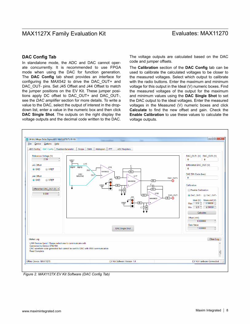
DAC Config TabIn standalone mode, the ADC and DAC cannot oper-ate concurrently. It is recommended to use FPGA mode when using the DAC for function generation. The DAC Config tab sheet provides an interface for configuring the MAX542 to drive the DAC_OUT+ and DAC_OUT- pins. Set J45 Offset and J44 Offset to match the jumper positions on the EV Kit. These jumper posi-tions apply DC offset to DAC_OUT+ and DAC_OUT-, see the DAC amplifier section for more details. To write a value to the DAC, select the output of interest in the drop-down list, enter a value in the numeric box and then click DAC Single Shot. The outputs on the right display the voltage outputs and the decimal code written to the DAC.
The voltage outputs are calculated based on the DAC code and jumper offsets. The Calibration section of the DAC Config tab can be used to calibrate the calculated voltages to be closer to the measured voltages. Select which output to calibrate with the radio buttons. Enter the maximum and minimum voltage for this output in the Ideal (V) numeric boxes. Find the measured voltages of the output for the maximum and minimum values using the DAC Single Shot to set the DAC output to the ideal voltages. Enter the measured voltages in the Measured (V) numeric boxes and click Calculate to find the new offset and gain. Check the Enable Calibration to use these values to calculate the voltage outputs.
Figure 2. MAX1127X EV Kit Software (DAC Config Tab)

Maxim Integrated │ 9www.maximintegrated.com
Evaluates: MAX11270MAX1127X Family Evaluation Kit
Function GeneratorWhen using the FPGA mode, the Function Generator tab allows the user to generate a signal with the DAC. Select the Number of Samples, DAC Update Rate, and Signal Frequency. Click Calculate to get the Adjust Frequency for the DAC signal needed for coherent sam-pling. Then select the Signal Type, Amplitude, Phase, and Offset to set up the waveform desired for the DAC. Click
Generate to find the DAC codes for the waveform and generate the waveform on the DAC. The waveform codes sent to the DAC is displayed on the graph. The Average, RMS, Maximum, Minimum, and Peak to Peak are also calculated and displayed on the right. To save the DAC code waveform, go to Options > Save Graph > Function Generator. This saves the settings on the left and the data in the graph to a csv file.
Figure 3. MAX1127X EV Kit Software (Function Generator Tab)

Maxim Integrated │ 10www.maximintegrated.com
Evaluates: MAX11270MAX1127X Family Evaluation Kit
Scope TabThe Scope tab sheet is used to capture data and dis-play it in the time domain. Sample Rate and Number of Samples can also be set in this tab if they were not appropriately adjusted in other tabs. The Display Unit drop-down list allows counts and voltages. Once the desired configuration is set, click on the Capture button. The right side of the tab sheet displays details of the wave-
form, such as Average, Standard Deviation, Maximum, Minimum, and Fundamental Frequency. Figure 4 displays the ADC data when a sinusoidal signal is applied at the inputs on the EV kit.To save the captured data to a file, go to Options > Save Graph > Scope. This saves the setting on the left and the data captured to a csv file.
Figure 4. MAX1127X EV Kit Software (Scope Tab)

Maxim Integrated │ 11www.maximintegrated.com
Evaluates: MAX11270MAX1127X Family Evaluation Kit
DMM TabThe DMM tab sheet provides captured data as a digital multimeter. Once the desired configuration is set, click on the Capture button. Figure 5 displays the results shown
by the DMM tab when ADC_INP and ADC_INN (J26 and J27 set as 7-8) are set to REF, see Table 2 for jumper positions.
Figure 5. MAX1127X EV Kit Software (DMM Tab)

Maxim Integrated │ 12www.maximintegrated.com
Evaluates: MAX11270MAX1127X Family Evaluation Kit
Histogram TabThe Histogram tab sheet is used to display a histogram of the captured data. Sampling rate and number of samples can also be set in this tab if they were not appropriately adjusted in other tabs. Once the desired configuration is set, click on the Capture button. The right side of the tab sheet displays details of the histogram such as Average, Standard Deviation, Maximum, Minimum, Peak-to-Peak
Noise, Effective Resolution, and Noise-Free Resolution. To use this histogram feature, apply a DC voltage at the input. Figure 5 displays the results shown by the DMM tab when ADC_INP and ADC_INN are set to REF, see Table 2 for jumper positions.To save the histogram data to a file, go to Options > Save Graph > Histogram. This saves the setting on the left and the histogram data captured to a csv file.
Figure 6. MAX1127X EV Kit Software (Histogram Tab)

Maxim Integrated │ 13www.maximintegrated.com
Evaluates: MAX11270MAX1127X Family Evaluation Kit
FFT TabThe FFT tab sheet is used to display the frequency domain FFT of the captured data. Sample Rate and Number of Samples can also be set in this tab if they were not appro-priately adjusted in other tabs. Once the desired configura-tion is set, click on the Capture button. The right side of
the tab displays the performance based on the FFT, such as Fundamental Frequency, THD, SNR, SINAD, SFDR, ENOB, and Noise Floor.To save the FFT data to a file, go to Options > Save Graph > FFT. This saves the setting on the left and the FFT data captured to a csv file.
Figure 7. MAX1127X EV Kit Software (FFT Tab)

Maxim Integrated │ 14www.maximintegrated.com
Evaluates: MAX11270MAX1127X Family Evaluation Kit
ADC Registers TabThe ADC Registers tab sheet shows the ADC registers on the left. The middle section shows the bits and bit descriptions of the selected register. Click Read All to read all registers and refresh the window with the register settings. To write a register first, select the hex value in the Value (Hex) column, type the desired hex value and press Enter.
The Command Byte is on the right side of the tab sheet. This byte precedes all SPI transactions and is described in the ADC data sheet. To send a command byte, enter a hex value in the Numeric box and click the Send button. The command byte has two different formats including Conversion Mode and Register Access Mode. Select the radio button for the desired mode to see the bit descrip-tion in the table.
Figure 8. MAX1127X EV Kit Software (ADC Registers Tab)

Maxim Integrated │ 15www.maximintegrated.com
Evaluates: MAX11270MAX1127X Family Evaluation Kit
Detailed Description of HardwareThis EV kit provides a proven layout to demonstrate the performance of the MAX1127X 24-bit delta-sigma ADC. Included in the EV kit are digital isolators (MAX14934), ultra-low-noise LDOs (MAX8842) to all supply pins of the IC, an on-board reference (MAX6126), a precision amplifier (MAX44241) for the analog inputs, 16-bit DAC (MAX542) with precision amplifiers (MAX9632), and sync-in and sync-out signals for coherent sampling. An on-board controller is provided to allow for evaluation in standalone mode, which has limitations on maximum sample size and it cannot perform coherent sampling. The EV kit can be used with FPGA mode to achieve larger sample depth and coherent sampling.The ADC has several input options which are selected by J26 and J27. The external option allows for wires attached to the screw terminals at J10. The amplifier option allows for signals at testpoints CH_A to CH_D. The DAC option allows for inputs to be driven from an on-board DAC. The REF options connect the inputs to the voltage reference of the ADC.
User-Supplied SPITo evaluate the ADC on this EV kit with a user-supplied SPI bus, disconnect from the FMC bus and remove jumper J20. Apply the user-supplied SPI signals to SCLK, CSB, DIN, and DOUT at the PMOD_A header (J32). Make sure the return ground is connected to PMOD ground. To communicate to the on-board DAC connect the user-supplied SPI signals to CSB, SCLK, DIN, and LDAC at the PMOD_B header (J33). Make sure the return ground is connected to PMOD ground.The on-board FTDI chip used for standalone mode does not conflict with the user-supplied SPI if it is powered off by removing jumper J20.Caution: Do not plug this header into a standard PMOD interface found on other FPGA or microcontroller prod-ucts. The signal definition is unique to this EV kit.
User-Supplied ReferenceFor user-supplied reference voltage, set jumpers at J21 and J23 to positions 2-3 and apply external reference to either J9 or to the EXT_REFN and EXT_REFP testpoints.
User-Supplied AVSS The AVSS supply is set to GND or -1.8V by Jumper J5. For user-supplied AVSS, remove the jumper from J5 and apply AVSS to the screw-terminals/testpoint at J13. Make sure that this external supply has the correct relation to system ground.
User-Supplied AVDD The AVDD supply is set to 3.6V or 1.8V by jumper J8. For user-supplied AVDD, remove the jumper from J8 and apply AVDD to the screw-terminals/testpoint at J13. Make sure that this external supply has the correct relation to system ground.
Bipolar Powered vs. Unipolar PoweredThe ADC supports both unipolar and bipolar ranges. For unipolar mode, jumper J8 pins 2-3 to power AVDD with 3.6V and jumper J5 pins 1-2 to set AVSS to GND. For bipolar mode, jumper J8 pins 1-2 to power AVDD with 1.8V and jumper J5 pins 2-3 to set AVSS to -1.8V.
External Clock When the ADC is configured to use an external clock, Jumper J36 pins 2-3 to select the on-board oscillator as the clock source. Jumper J36 pins 1-2 to select the SMA connector (and user-provided clock) as the clock source.
GPIO Testpoints are provided for the three GPIO signals from the ADC, GPIO1, GPIO2, and GPIO3. The ADC Config tab can configure these as input/output and read/drive the GPIO pins. GPIO1 connects to a FET which allows J14.1 and TP2 to be connected to ground by driving GPIO1 high (note that DVDD should be to 3.3V to drive the FET).
ADC Input AmplifiersThe input amplifiers allow for significant flexibility. The amplifier input stage begins with testpoints labeled CH_A to CH_D. Each set of testpoints has options to ground either the inverting or noninverting inputs. The jumper block J29 and J25 allow for bypassing the first stage of amplifiers, or connecting the first stage to the second stage. Jumper J7 can provide an offset of 2.5V to the CH_A/CH_B signals – leave unpopulated to have an offset of 0V. Similarly, jumper J6 can provide an offset of 2.5V to the CH_C/CH_D signals – leave unpopulated to have an offset of 0V.
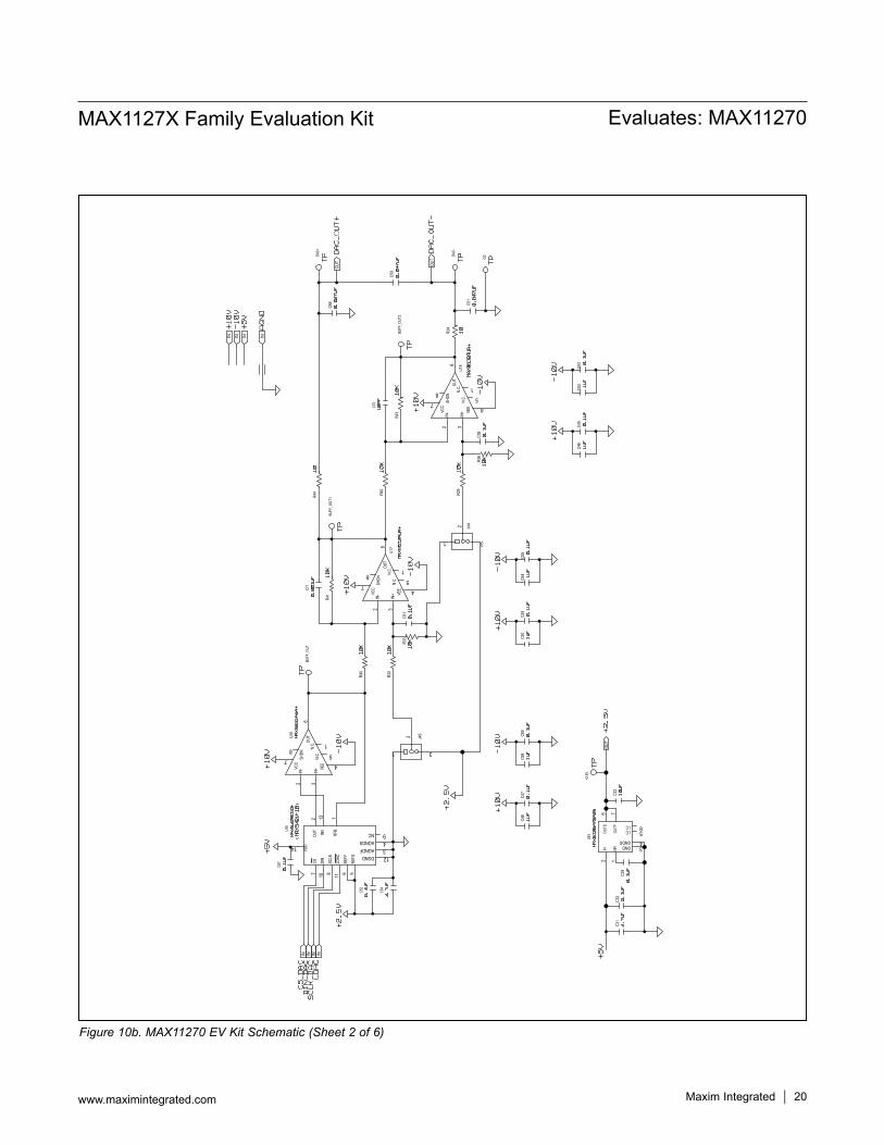
DAC and DAC AmplifiersIn Figure 2, the GUI shows a functional diagram of the DAC and DAC amplifiers. Here jumper J45 can be con-nected to 2.5V to add a 2.5V offset to the DAC_OUT+ signal, and J44 can be connected to 2.5V to add 2.5V to the DAC_OUT- signal.The value at DAC_OUT+ and DAC_OUT- are available to drive to the ADC by use of jumpers J26 and J27.Also, please note that the DAC_OUT+ and DAC_OUT- values shown by the GUI are only valid if the settings at J44 and J45 are the same on both the PCB and the GUI.

Maxim Integrated │ 16www.maximintegrated.com
Evaluates: MAX11270MAX1127X Family Evaluation Kit
Figure 9. Analog Front-End
-
+
MAX44241 ADC_INP
+2.5V
J29J271
3
57
1 2
3 4
5 67 8
MAX44241
CH_A-
CH_A+
CH_B-
CH_B+
-
+
J281 23 4
J301 23 4
MAX44241 2
4
68
9 10
ADC_REFP
J7
IN+
DAC_OUT+ADC_REFP
-
+
MAX44241 ADC_INN
+2.5V
J25J261
3
57
1 2
3 4
5 67 8
MAX44241
CH_C-
CH_C+
CH_D-
CH_D+
-
+
J241 23 4
J221 23 4
MAX44241 2
4
68
9 10
ADC_REFP
J6
IN-
DAC_OUT-ADC_REFN
MAX1127xSigma-Delta ADC
ADC_REF/2

Maxim Integrated │ 17www.maximintegrated.com
Evaluates: MAX11270MAX1127X Family Evaluation Kit
Table 4. Analog Input Configurations (Ch A - D)CONFIGURATION SIGNAL-PATH INPUT
CONFIGURATION INPUT CONNECTORS JUMPER POSITIONSNo. DESCRIPTION
1 Channel A and CNoninverting, differential,
second-order LPF (default)
CH_A- and CH_C-
J28: 3-4J30: 3-4J24: 3-4J22: 3-4
J29: 1-2 and 7-8J25: 1-2 and 7-8
J26: 3-4J27: 3-4
J7: 1-2 (for bipolar signal) or Open for unipolar signal
J8: 1-2 (for bipolar signal) or Open for unipolar signal
2 Channel A and C Inverting, differential, second-order LPF CH_A+ and CH_C+
J28: 1-2J30: 3-4J24: 1-2J22: 3-4
J29: 1-2 and 7-8J25: 1-2 and 7-8
J26: 3-4J27: 3-4
J7: 1-2 (for bipolar signal) or Open for unipolar signal
J8: 1-2 (for bipolar signal) or OPEN for unipolar signal
3 Channel B and D Noninverting, differential, first-order LPF CH_B+ and CH_D+
J28: 1-2 and 3-4J30: 1-2
J24: 1-2 and 3-4J22: 1-2
J29: 3-4 and 7-8J25: 3-4 and 7-8
J26: 3-4J27: 3-4
J7: 1-2 (for bipolar signal) or Open for unipolar signal
J8: 1-2 (for bipolar signal) or Open for unipolar signal
4 Channel B and D Inverting, differential, first-order LPF CH_B- and CH_D-
J28: 1-2 and 3-4J30: 3-4
J24: 1-2 and 3-4J22: 3-4
J29: 3-4 and 7-8J25: 3-4 and 7-8
J26: 3-4J27: 3-4
J7: 1-2 (for bipolar signal) or Open for unipolar signal
J8: 1-2 (for bipolar signal) or Open for unipolar signal

Maxim Integrated │ 18www.maximintegrated.com
Evaluates: MAX11270MAX1127X Family Evaluation Kit
Table 4. Analog Input Configurations (Ch A - D) (continued)CONFIGURATION SIGNAL-PATH INPUT
CONFIGURATION INPUT CONNECTORS JUMPER POSITIONSNo. DESCRIPTION
5 External Inputs User-supplied signals IN+ and IN-
J28: 1-2 and 3-4J30: 1-2 and 3-4J24: 1-2 and 3-4J22: 1-2 and 3-4J29: 3-4 and 7-8J25: 3-4 and 7-8
J26: 1-2J27: 1-2J7: OpenJ8: Open
6 DAC Output DAC output buffered with MAX9632
DAC_OUT+ and DAC_OUT-
J28: 1-2 and 3-4J30: 1-2 and 3-4J24: 1-2 and 3-4J22: 1-2 and 3-4J29: 3-4 and 7-8J25: 3-4 and 7-8
J26: 5-6J27: 5-6J7: OpenJ8: Open
7 ADC Voltage Reference
Voltage reference input to ADC from MAX6126 or external source (see J21
and J23)
ADC_REFP and ADC_REFN
J28: 1-2 and 3-4J30: 1-2 and 3-4J24: 1-2 and 3-4J22: 1-2 and 3-4J29: 3-4 and 7-8J25: 3-4 and 7-8
J26: 7-8J27: 7-8J7: OpenJ8: Open

Maxim Integrated │ 19www.maximintegrated.com
Evaluates: MAX11270MAX1127X Family Evaluation Kit
Figure 10a. MAX11270 EV Kit Schematic (Sheet 1 of 6)
MAX
1127
0EUG
+
BYRE
WOR
KON
REVA
PCB
D3AN
DD4
ARE
ADDE
D
DNI
EXTE
RNAL
CLOC
KSM
ACO
NNEC
TOR
0.1UF
SCLK
_ADC
0.01U
F49
.9
OPEN
+3.3V
FXO-
HC73
0-8.
192
*
RDYB
_ADC
-1.8
V
PCC0
2SAA
N
+3.3
V
10K 10
00PF
MAX6
126A
ASA2
5
7339
1-006
0
ADC_
INN
ADC_
INP
BAT54S
AVSS
AVDD
BAT54S
TP
DVDD
_ADC
AVSS
0
AVDD
*
+1.8
VAV
SS
SYNC
_ADC
DOUT
_ADC
DIN_
ADC
EXT_
REFP
EXT_
REFN
DAC_
OUT-
1000
PF
28
GPIO
1GP
IO2
GPIO
3
1000
PF
AVDD
AVSS
+3.3
V
-1.8
V
DAC_
OUT+
0
CS_A
DC
+1.8
V
DVDD
_ADC
EXT_
REFP
0.01U
F
+2.0
V
0
1UF
+2.0
V
+3.3V
AGND
TP
ADC_
REFP
ADC_
REFN
0.01U
F
TP
0.01U
F
0.1UF
49.9
CLK
0.1UF
ADC_
REFP
0.1UF
49.9
0.1UF
*
1000
PF0.0
1UF
OPEN
A3.6
VTP
TP
OPEN
TP
4.7UF
AVSS
0.1UF
EXT_
REFN
TP
PCC02SAAN
0
10K
ADC_
REFN
A3.6
V
ADC_
INP
ADC_
REFP
IN
OUTF
OUTS
NR
CB5
C108
C109
R71
R70
C114
C106
REFN
REFP
SCLK CS
B
DVDD
CAPR
EG
DGND CL
K
RDYB
/ICLK
AVSS
CAPP
CAPN
AINP
AINN
AVSS
AVDD
GPIO
1/MB1
GPIO
2
GPIO
3/MSY
NC
RSTB
SYNC
DGND
DOUT
/MB0
DIN
VDD
OUTP
UT GND
E/D
D4
D3
I.C.I.C.
GNDSGND
IN
OUT
OUTIN
OUT
INININ IN IN
OUT
OUT
OUT
OUT
OUT
INININ IN
IN
ININ
IN
ININ
IN
C93
ADC_
CAPR
C84
G4
C77
J34
C81
C80
U21
ADC_
REFN
ADC_
INN
GPIO
1
3
1920
224 23
1
33
2
22
2
21
31
2
1
6 712
22
4 5
14 13186 7 8
22 21 16 1517
109 1211
J11
U25
C85
C115
C96
CB4
R55
C95
J8
J5J4
J40
J37
R63
C86
C83
C87
R49
J36 U2
0
J23
R61
C82
J21
R53
R60
R56
CB6
R72
21
2 1
2 1
31
3131
31
4 2
31
5342
85
43
3 1 31
Maxim Integrated │ 20www.maximintegrated.com
Evaluates: MAX11270MAX1127X Family Evaluation Kit
Figure 10b. MAX11270 EV Kit Schematic (Sheet 2 of 6)
(MAX
542V
-18)
MAX5
42AE
SD+
-10V
10K
TP
TP
0.001
UF
TP
10PF
TPTPTP
+10V
10
10K
MAX9
632A
UA+
-10V
+10V
MAX9
632A
UA+
0.047
UF
-10V
+10V
-10V
10K
0.1UF
1UF
0.1UF
0.1UF
1UF
+10V
0.1UF
CS_D
ACSC
LK_D
AC
MAX9
632A
UA+
+10V
-10V
+5V
-10V
-10V
1UF
10
+5V
4.7UF
0.1UF
10UF
AGND
+5V
+10V
4.7UF
DIN_
DAC
LDAC
+2.5
V
+10V
1UF
0.1UF
0.1UF
MAX6
126A
ASA2
5
0.1UF
0.1UF
10K
1UF
1UF
0.1UF
0.1UF
+2.5
VTP
+2.5
V10
K
10K
10K
0.1UF
0.047
UF
DAC_
OUT-
DAC_
OUT+
10K
0.047
UF
C52
+2.5V
U10
C67
C54
C72
C71
U15
G2DAC-
DAC+
BUFF
_OUT
2
BUFF
_OUT
1
BUFF
_OUT
IN
OUTF
OUTS
NR
J44
J45
C31
C32
C39
C23
C46
C45
C62
C63
C50
C49
C64
C65
C69
C68
C47
C48
C51
R34
C59
C66
R44 R2
9
R42
R36
C58
R43
U18
R41
C61
R33
R30
R40
U17
U16
N.C.
N.C.
SHDN
VCC
VEE
OUT
IN+
IN-
N.C.
N.C.
SHDN
VCC
VEE
OUT
IN+
IN-
N.C.
N.C.
SHDN
VCC
VEE
OUT
IN+
IN-
OUT
VDD
INV
LDAC
DIN
SCLK
CS REFF
REFS
RFB I.C.
I.C.
GNDSGND
OUT
IN
IN
OUT
OUT
INININ
INININ
DGND
NCAGNDSAGNDF
2
2
6 712
62 3
62 3
81
56
2 1310 117
62 3
31
31
8543
47
85
1
47
85
1
14
9
12
43
47
85
1

Maxim Integrated │ 21www.maximintegrated.com
Evaluates: MAX11270MAX1127X Family Evaluation Kit
Figure 10c. MAX11270 EV Kit Schematic (Sheet 3 of 6)
CONF
IG
USB
U3
18PF
18PF
12MH
Z
+3.3
V_US
B
10K
12K
LDAC
_FPG
A
4.7K
28
SYNC
_ADC
_FPG
A2828
RDYB
_ADC
_FPG
A
GND
USB+
5V
15K
10K
28 28
+1.8
V10
1181
92-0
001L
F
2828 28 2828
0.1UF
FT22
32HL
4.7UF
DIN_
DAC_
FPGA
CS_D
AC_F
PGA
0.1UF
0.1UF
10K
+3.3
V_US
B
0.1UF
0.1UF
0.1UF
0.1UF
0.1UF
10K
2.2K
USB+
5V+3
.3V_
USB
10K10K
4.7UF
+3.3
V_US
B0.1
UF
2828
DOUT
_ADC
_FPG
ACS
_ADC
_FPG
A
93LC
66BT
-I/OT
10K10K10K
4.7UF
+3.3
V_US
B
+1.8
V
SCLK
_ADC
_FPG
ADI
N_AD
C_FP
GA
600
+3.3
V_US
B
10K
SCLK
_DAC
_FPG
A
+3.3
V_US
B
USB+
5V
C21
C18
C22
C29
C14
C17
C30
C15
C19
C16
C20
L3
CB2
CB3
YB1
C24
DSB1
2 1
RB23RB
26
RB25
R1R2
J1
RB10
RB15
UB1
RB5
RB4
RB3
RB17
RB19
RB16
RB18
RB14
RB12
RB7
RB9
UB2
SHIE
LD54321
VCC
VSS
DO
DI
CLKCS
BCBU
S7
BCBU
S6
BCBU
S5
BCBU
S4
BCBU
S3
BCBU
S2
BCBU
S1
BCBU
S0
ACBU
S7
ACBU
S6
ACBU
S5
ACBU
S4
ACBU
S3
ACBU
S2
ACBU
S1
ACBU
S0
BDBU
S7
BDBU
S6
BDBU
S5
BDBU
S4
BDBU
S3
BDBU
S2
BDBU
S1
BDBU
S0
ADBU
S7
ADBU
S6
ADBU
S5
ADBU
S4
ADBU
S3
ADBU
S2
ADBU
S1
ADBU
S0
OSCO
OSCI
EECS
EECL
K
EEDA
TA
TEST
VREG
OUT
VREG
IN
RESE
T#
SUSP
END#
PWRE
N#
DPDM REF
OUT
OUT
OUT
OUT
OUT
IN
INININ ININ OUTIN
RB22RB21
RB6RB8RB11RB13RB24RB20
VCORE
GNDGND
VCCIO
VCOREVCORE
GNDGND
VCCIO
GNDGND
VCCIO
GNDGND
VCCIO
VPLL
AGNDVPHY
4 5321
135 4
4950 1336
146
60326163 6287
4645444341403938 59585755545352482423222119181716 3433323029282726
1110
9876
2 1
26
KA
94
643712
56423120
51473525151151
10
Maxim Integrated │ 22www.maximintegrated.com
Evaluates: MAX11270MAX1127X Family Evaluation Kit
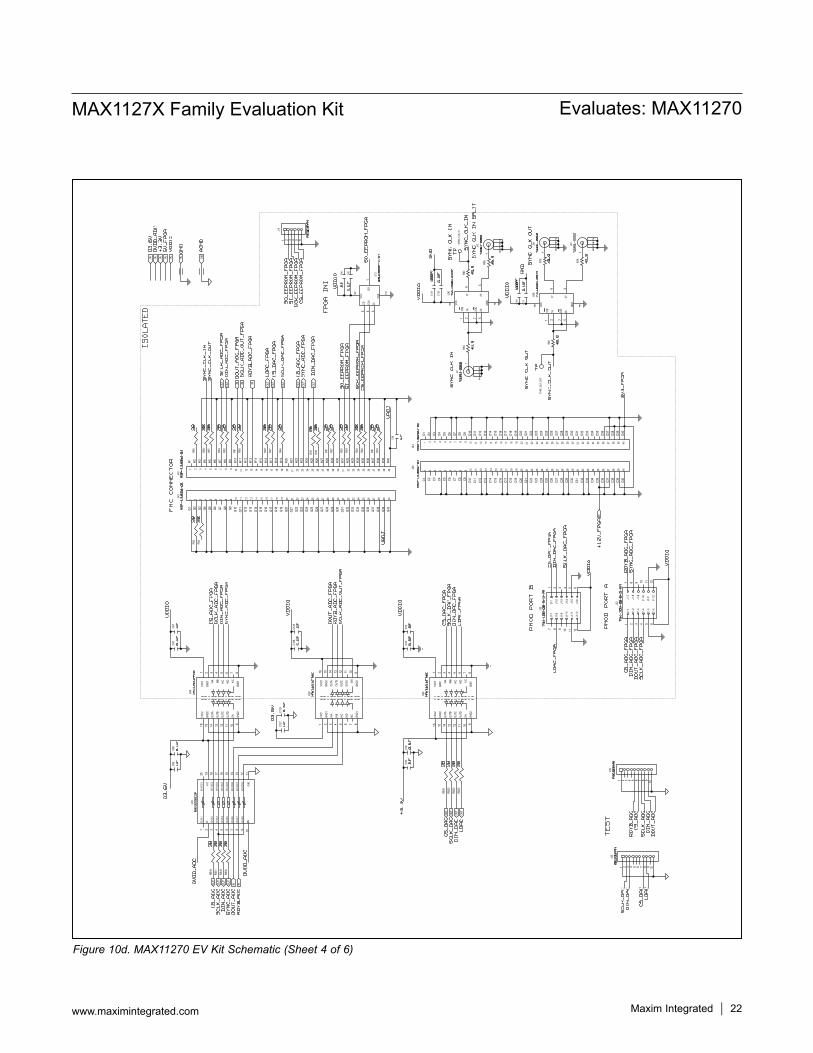
Figure 10d. MAX11270 EV Kit Schematic (Sheet 4 of 6)
MAX
1493
4FAW
E
FPGA
INI
SYNC
CLK
IN
ISOL
ATED
FMC
CONN
ECTO
R
PMOD
PORT
A
SYNC
CLK
INSP
LIT
SYNC
CLK
OUT
SYNC
CLK
OUT
SYNC
CLK
IN
TEST
PMOD
PORT
B
MAX
1493
4FAW
E
MAX
1493
4FAW
E
SCLK
_DAC
_FPG
ACS
_DAC
_FPG
A
+3.3
V
VDDI
O
D3.6
V
0.1UF
1UF
SYNC
_ADC
_FPG
ARD
YB_A
DC_F
PGA
VDDI
O
DIN_
DAC_
FPGA
LDAC
DIN_
DAC
CS_D
AC
SCLK
_DAC
_FPG
A
DIN_
DAC_
FPGA
CS_D
AC_F
PGA
LDAC
_FPG
A
28
SCLK
_DAC
LDAC
_FPG
A
DOUT
_ADC
_FPG
A
CS_A
DC_F
PGA
VDDI
O
VDDI
O
SCK_
EEPR
OM_F
PGA
CS_E
EPRO
M_F
PGA
SI_E
EPRO
M_F
PGA
28
SCLK
_ADC
_OUT
_FPG
A
0.1UF
SYNC
_CLK
_OUT
SYNC
_CLK
_IN
49.9
RDYB
_ADC
_FPG
A
SYNC
_CLK
_OUT
SCLK
_ADC
_FPG
ADI
N_AD
C_FP
GA
DOUT
_ADC
_FPG
A
28
ASP-
1346
04-0
11U
F DIN_
ADC_
FPGA
GND
AGND
PBC0
6SAA
N
SO_E
EPRO
M_F
PGA
PBC1
0SAA
N
SCLK
_ADC
_FPG
ADO
UT_A
DC_F
PGA
DIN_
ADC_
FPGA
CS_A
DC_F
PGA
SCLK
_DAC
_FPG
A
CS_A
DC_F
PGA
DIN_
DAC_
FPGA
VADJ
VADJ
LDAC
_FPG
A
28
SYNC
_ADC
_FPG
A
282828 2828
1UF
ASP-
1346
04-0
1
28 28
VDDI
O
+3.3
V5V
_FPG
A
28 2828 28 28 28
DVDD
_ADC
D3.6
V
28
CS_D
AC_F
PGA
93LC
66BT
-I/OT
SCLK
_ADC
_OUT
_FPG
ARD
YB_A
DC_F
PGA
SO_E
EPRO
M_F
PGA
SI_E
EPRO
M_F
PGA
SCK_
EEPR
OM_F
PGA
CS_E
EPRO
M_F
PGA
VDDI
O1U
F
0.1UF
282828SY
NC_C
LK_I
N28
PBC1
0SAA
N
RDYB
_ADC
DOUT
_ADC
DIN_
ADC
SCLK
_ADC
LDAC
CS_A
DC
SO_E
EPRO
M_F
PGA
74LV
C2G1
25DP
49.9
7339
1-006
0
TP
1000
PF
0.1UF
49.9
7339
1-006
0
49.9
7339
1-006
0
49.9
1000
PF
74LV
C2G1
25DP
0.1UF
TP
VDDI
O
VDDI
O
GND
GND
7339
1-006
0
1UF
1UF
1UF
1UF
0.1UF
MAX3
002E
UP
28 28 28
2828
DVDD
_ADC
D3.6
V
DVDD
_ADC
DIN_
DAC
SCLK
_ADC
CS_A
DC
DIN_
ADC
SYNC
_ADC
RDYB
_ADC
DOUT
_ADC
49.9
3V3_
FPGA
ASP-
1346
04-0
1AS
P-13
4604
-01
+12V
_FPG
A
TSW
-106
-08-
S-D-
RA
VDDI
O
28
0.1UF
SCLK
_ADC
_FPG
A
SYNC
_ADC
_FPG
A
0.1UF
28 28SC
LK_D
ACCS
_DAC
0.1UF
TSW
-106
-08-
S-D-
RA
UB3
C116
J38
J41
C111
C131
C130
J42SY
NC_C
LK_IN
SYNC
_CLK
_OUT
J31
J19
C44
C42
C38
I/O V
CC1
VCC
I/O V
CC2
I/O V
CC3
I/O V
CC4
I/O V
CC5
I/O V
CC6
I/O V
CC7
I/O V
CC8
GND
ENI/O V
L8
I/O V
L7
I/O V
L6
I/O V
L5
I/O V
L4
I/O V
L3
I/O V
L2
VLI/O V
L1
U22
J43
J43
J43
J43
U29U3
4
C92
RB33
RB48
C76
C79
C78
C75
RB32
RB31
RB35
C127
C129
C128
C126
RB50
RB49
RB51
J35
J33
U30
R75
R78
U28
R83
R85
R80
R84
C91
C97
J39
C98
U12
R57
R58
R65
R52
R54
R50
R51
R47
R48
R46
R37 R2
7
R31
R35 R2
4
R25
R22
R23
R19
R21
R59
R62
J32
40393837363534333231302928272625242322212019181716151413121110987654321
40393837363534333231302928272625242322212019181716151413121110987654321
40393837363534333231302928272625242322212019181716151413121110987654321
40393837363534333231302928272625242322212019181716151413121110987654321
GND2
GND2
CN
NEVCC2
OUTA
OUTB
OUTC
OUTD
GND1IN
D
INCINB
INA
GND1
VCC1
GND2
GND2 EN
NC
VCC2
OUTA
OUTB
OUTC
OUTD
GND1
IND
INC
INB
INA
GND1
VCC1
GND2
GND2
CN
NEVCC2
OUTA
OUTB
OUTC
OUTD
GND1IN
D
INCINB
INA
GND1
VCC1
J1-1
2
J1-1
1
J1-1
0
J1-9
J1-8
J1-7
J1-6
J1-5
J1-4
J1-3
J1-2
J1-1
2A2OE
2Y
VCC
1Y
GND
1A1OE
2A2OE
2Y
VCC
1Y
GND
1A1OE
VCC
VSS
DO
DICLK
CS
J1-1
2
J1-1
1
J1-1
0
J1-9
J1-8
J1-7
J1-6
J1-5
J1-4
J1-3
J1-2
J1-1
IN IN
INININ
OUT
OUT
OUT
OUT
OUT
OUT
OUT
OUT
OUT
OUT
IN
IN
IN
OUT
INININ
OUT
OUT
OUTIN
OUT
OUT
C6 C7 C10
C11
C12
912 98765431
1213141516171820 1110
C40
C39
C38
C37
C36
C35
C34
C33
C32
C31
C30
C29
C28
C27
C26
C25
C24
C23
C22
C21
C20
C19
C18
C17
C16
C15
C14
C13C9C8C5C4C3C2C1
D40
D39
D38
D37
D36
D35
D34
D33
D32
D31
D30
D29
D28
D27
D26
D25
D24
D23
D22
D21
D20
D19
D18
D17
D16
D15
D14
D13
D12
D11
D10
D9D8D7D6D5D4D3D2D1
G40
G39
G38
G37
G36
G35
G34
G33
G32
G31
G30
G29
G28
G27
G26
G25
G24
G23
G22
G21
G20
G19
G18
G17
G16
G15
G14
G13
G12
G11
G10G9G8G7G6G5G4G3G2G1
H40
H39
H38
H37
H36
H35
H34
H33
H32
H31
H30
H29
H28
H27
H26
H25
H24
H23
H22
H21
H20
H19
H18
H17
H16
H15
H14
H13
H12
H11
H10
H9H8H7H6H5H4H3H2H1
161 11121314
7654315
89
2
10
161
11121314
7654315 9
82
10161 11121314
7654315
89
2
10
121110987
654321
35
62 71
1 1
35
62 71
1
1
135 4
10987654321
10987654321
654321
121110987
654321
IN
8 4
5342
5342
8 4
5342
5342
26

Maxim Integrated │ 23www.maximintegrated.com
Evaluates: MAX11270MAX1127X Family Evaluation Kit
Figure 10e. MAX11270 EV Kit Schematic (Sheet 5 of 6)
TERM
INAL
BLOC
KS
REVA
OFM
AX11
270E
VKIT
DOES
NOT
HAVE
R86
AND
R87
AND
J27.
9IS
ASSI
GNED
TOGN
D,NO
TAD
C_RE
F/2
ADC_
INN
ADC_
REFP
DAC_
OUT+
ADC_
REF/
2
10
ADC_
REFP
ADC_
REF/
2
10K
ADC_
INP
ADC_
REFN
1000
PF
PBC0
5DAA
N
EXT+
AMP+
PBC0
5DAA
N
10
EXT_
REFP
EXT_
REFN
+10V
-10V
AGND
ADC_
REFP
AMP-
49.9
+2.5
V
MAX4
4241
AUK+
0.1UF
PBC0
4DAA
N
1UF
TP
TPEX
T_RE
FN
2N70
02
100
TP
AVSS
AVDD
PBC0
4DAA
N
+2.5
V
-10V
MAX4
4241
AUK+
-10V
MAX4
4241
AUK+
1000
PF
1000
PFMA
X442
41AU
K+
-10V
TP TPTP
10K
1000
PF
10K
1000
PF
1UF
+10V +10V
IN-
ADC_
REFP
OSTT
A020
161
IN-
IN+
+10V
1000
PF
10K
0.1UF
1UF
-10V
TP
10K
10K
TP
10K
10K
TP TP0
-10V
0.1UF
10K
10K
1000
PF
10K
TPTP
IN+
TP
TP
0
TP0 0
0
1M 1M
4.99
10K
1UF
4.99
0.1UF
10K
10K
1M 1M1M
TP
10K
1M1M
TP TPTP
10K
1UF
10K
1000
PF
1M
1000
PF
+10V
-10V
100K
100K
100
GPIO
2GP
IO3
1UF
100
GPIO
1
AVDD
AVSS
+10V
-10V
DAC_
OUT+
0.1UF
1UF
0.1UF
1UF+1
0V
DAC_
OUT-
TPTP
OSTT
A020
161
OSTT
A020
161
TPEX
T_RE
FP
0.1UF
10K
+10V
0.1UF
10K
-10V
49.9
OSTT
A020
161
100K
PBC0
3SAB
N
+10V
PBC0
3SAB
N
DAC_
OUT-
10K
EXT-
ADC_
REFN
C102
C118
A_IN
P1
C124
C99
C107
J28
J30
J24
J22
G3
J26
J27
J14
J13
J9J10
87
651 3
42 87
651 3
42
43
21
43
21
43
21
43
21
RB47
RB43
R82
R76
RB62
R67
RB59
R79
RB55
RB57
R73
R74
R77
R66
RB44
RB40
RB42
R69
R64
R68
RB54
RB53
RB52 RB
56
RB65
RB63
RB38
RB39
RB37
RB41
RB34
RB36
RB60
RB30
RB27
RB28
C88
C100
C103
C90
C112
C121
C119
C110
C117
C120
C123
C113
C101
C104
C94
C89
RB61
RB64
R81
RB66
RB58
RB46
RB45
VSS
VDD
INA-
INA+
OUTA
VSS
VDD
INA-
INA+
OUTA
VSS
VDD
INA-
INA+
OUTA
VSS
VDD
INA-
INA+
OUTA
GSD
ININ ININOUT
OUT
OUT
OUT
IN
IN
ININ
IN
IN IN
OUT
OUT
C122
U27
A_IN
P2
C125
J29
U26
U24
C_IN
P2
J25
U23
C_IN
P1
C105
QB1
C133
AVDD
EXT_
REFN
EXT_
REFP
IN+
GPIO
3
GPIO
2
IN-
CH_D
+
CH_D
-
CH_C
+
CH_C
-
CH_B
+
CH_B
-
CH_A
+
CH_A
-
AVSS
TP2
10
109
87
65
43
21
98
76
54
32
1
2121
2121
2 2
14 3
87
65
43
21
14 3
14 3
87
65
43
21
14 3
43
21
43
21
43
21
43
21
1
R87
R86
J7
J6
31 31
25
25
25
25
23

Maxim Integrated │ 24www.maximintegrated.com
Evaluates: MAX11270MAX1127X Family Evaluation Kit
Figure 10f. MAX11270 EV Kit Schematic (Sheet 6 of 6)
ISOLA
TED
USB P
OWER
TERM
INAL
BLOC
K
MAX1
3256
ATB+1K
MBR0
520L
10UF
TPPCC0
2SAA
N
PBC0
3SAB
N
0.1UF
MAX1
5006
CATT
+
180P
F
0
TP
169K
105K
0
1UF
715K
0.1UF
1UF
0.1UF
0.1UF
100K
0.1UF
100K
TP
TP
TP
237K
1UF
237K
MAX8
842E
LT+
453K
6.04K
1UF
TP
453K
1UF
MAX8
842E
LT+
TP
1UF
6.04K
0.1UF
MAX1
5006
AATT
+
KLDX
-0202
-B
OSTT
A020
161
MBR0
520L
TP
0.47U
F10
UF
1K
1K
TGM-
H240
V8LF
BAS4
002A
-RPP
600
1UF
600
TP
1UF
TP
60060
0
1UF
1UF
TP
PBC0
3SAB
N
MAX1
5006
CATT
+
100K
TP 10UF
TP
1UF
10UF
237K
237K
TP
1UF
150K
1UF
MAX8
842E
LT+
MAX8
842E
LT+
1UF
TP
1UF
100K
MAX6
64ES
A
0.1UF
100
1UF
0.1UF
MAX1
5006
BATT
+
10UF
MAX1
5006
CATT
+
0
180P
F
BAS4
002A
-RPP
PCC0
2SAA
N
TP
39K
MBR0
520L
TP
10UF
1K0.1
UF
715K
+10V
C7
C13
-10V
G1
C40
R4 C5 R3 R8
U2
DB1
C4C3
C2
C9 R5
U5
R20
R18
+3.3V
C12
C11
C10
U11
C41
C43
DS2
L2
C1
L1 L5
C8
L4 +5V
C28
T1
DS1
U3
R6
U6
C33
C37
-1.8V C7
3
+12V
C70
G6
RB1
RB29
R39
R7
RB2
J15
R38
D1
D2
C36
R16
R10
C27
A3.6V
C74
R13
U9
C35
R15
R12
R9
U19
C26
+2.0V
U8
R14
C34
R11
C25D3
.6V
R17
U7
R45
J20
U14
C57
C56
C55
+1.8V
R26
R28
C6
R32
C60
C53
U13
J18
-10VE
XT
+10V
EXT
J2
-15VE
XT
+15V
EXT
J17
J3
U4
U1
CB1
J16
J46
J12
G5
+12V
_FPG
A
USB+
5V
+3.3V
-10V +5
V
AGND
GND
+5V
+2.0V
VDDI
O
+3V3
_USB D3.6V
+5V
+15V
+5V
VDDI
O
A3.6V
+12V
+5V
+15V
-1.8V
+15V
5V_F
PGA
+1.8V
-10V
+10V
21
21
3
2
1
3
2
1
21
CA
CA
6
5
1
2
43
6
5
1
2
43
6
5
1
2
43
21
65
3
21
4
7
6
5
1
2
43
65
43
21
65
43
21
4
3 2
14
3 2
1
6
3
21
4
5
7
6
3
21
4
5
7
6
3
21
4
5
7
21
21
21
21
8 76 543 21
KA
2
1
810
5
9
7
11
3
64
65
3
21
4
7
6174 53 2
8
CA
KA
3 21FB
OUT
NC
ININ
DNGPE
FBOU
T
NC
ININ
DNGPE
FBOU
T
NC
ININ
DNGPE
8 76 543 21
EP
ST1
GND2
ST2
GND1
FAUL
T
ITHEN CLK
VDD2
VDD1
OUT
OUT
NC
ININ
DNGPE
OUT
SHDN
FBOUT
NC
IN
GND
VIN-
SHDN
2SH
DN1
VSET
GND
VOUT
1VO
UT2
SENS
E
OUT
SHDN
FBOUT
NC
IN
GND
OUT
SHDN
FBOUT
NC
IN
GND
OUT
IN
OUT O
UTIN
OUT
OUT
OUT
NC
ININ
DNGPE
OUT
OUT
OUT
OUT
OUT
OUT
OUT
SHDN
FBOUT
NC
IN
GND
651 3
42
651 3
42
~ ~-+ D4
D3
D2
D1
~ ~-+ D4
D3
D2
D1
1 3 2

Maxim Integrated │ 25www.maximintegrated.com
Evaluates: MAX11270MAX1127X Family Evaluation Kit
Figure 11. MAX11270 EV Kit Component Placement Guide—Top Side
1”
Maxim Integrated │ 26www.maximintegrated.com
Evaluates: MAX11270MAX1127X Family Evaluation Kit
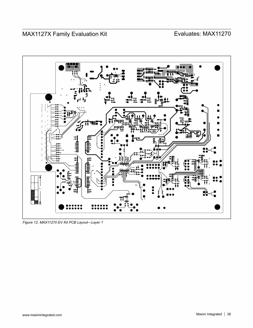
Figure 12. MAX11270 EV Kit PCB Layout—Layer 1
1”

Maxim Integrated │ 27www.maximintegrated.com
Evaluates: MAX11270MAX1127X Family Evaluation Kit
Figure 13. MAX11270 EV Kit PCB Layout—Layer 2
1”

Maxim Integrated │ 28www.maximintegrated.com
Evaluates: MAX11270MAX1127X Family Evaluation Kit
Figure 14. MAX11270 EV Kit PCB Layout—Layer 3
1”

Maxim Integrated │ 29www.maximintegrated.com
Evaluates: MAX11270MAX1127X Family Evaluation Kit
Figure 15. MAX11270 EV Kit PCB Layout—Layer 4
1”

Maxim Integrated │ 30www.maximintegrated.com
Evaluates: MAX11270MAX1127X Family Evaluation Kit
Figure 16. MAX11270 EV Kit PCB Layout—Layer 5
1”

Maxim Integrated │ 31www.maximintegrated.com
Evaluates: MAX11270MAX1127X Family Evaluation Kit
Figure 17. MAX11270 EV Kit PCB Layout—Layer 6
1”
Maxim Integrated │ 32www.maximintegrated.com
Evaluates: MAX11270MAX1127X Family Evaluation Kit
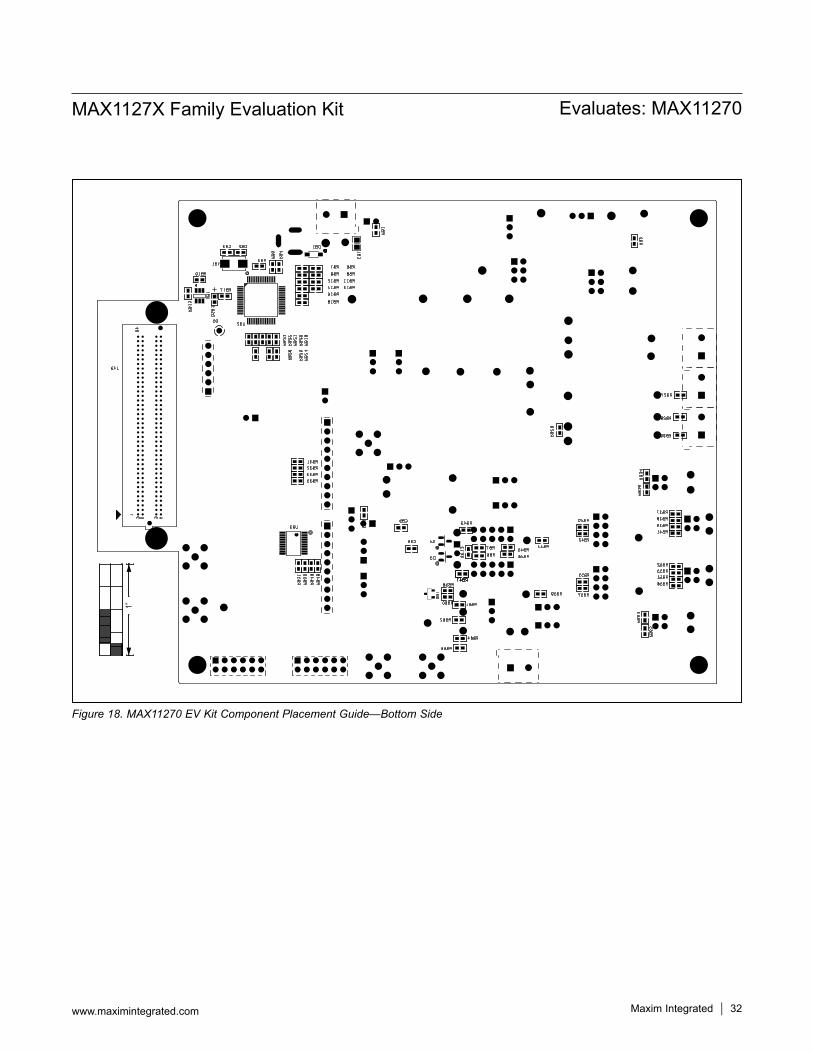
Figure 18. MAX11270 EV Kit Component Placement Guide—Bottom Side
1”

Maxim Integrated │ 33www.maximintegrated.com
Evaluates: MAX11270MAX1127X Family Evaluation Kit
#Denotes RoHS compliant.
Refer to file “evkit_bom_max11270_evkit_b.csv” attached to this data sheet for component information.
PART TYPEMAX11270EVKIT# EVKIT
Ordering InformationComponent List

Maxim Integrated cannot assume responsibility for use of any circuitry other than circuitry entirely embodied in a Maxim Integrated product. No circuit patent licenses are implied. Maxim Integrated reserves the right to change the circuitry and specifications without notice at any time.
Maxim Integrated and the Maxim Integrated logo are trademarks of Maxim Integrated Products, Inc. © 2015 Maxim Integrated Products, Inc. │ 34
Evaluates: MAX11270MAX1127X Family Evaluation Kit
REVISIONNUMBER
REVISIONDATE DESCRIPTION PAGES
CHANGED
0 4/15 Initial release —
Revision History
For pricing, delivery, and ordering information, please contact Maxim Direct at 1-888-629-4642, or visit Maxim Integrated’s website at www.maximintegrated.com.
Related Documents