Massively Broadband Wireless Communications and RFIC Design research at The University of Texas at Austin Professor Ted Rappaport and Felix Gutierrez 1 Wireless Networking and Communication Group Department of Electrical and Computer Engineering The University of Texas at Austin IEEE Joint Chapter of the Communications/Signal Processing Society, Austin, TX April 14, 2010 [wireless, felixgutierrez] @mail.utexas.edu

Welcome message from author
This document is posted to help you gain knowledge. Please leave a comment to let me know what you think about it! Share it to your friends and learn new things together.
Transcript
Massively Broadband Wireless
Communications and RFIC
Design research at The
University of Texas at Austin
Professor Ted Rappaport and Felix Gutierrez
1Wireless Networking and Communication Group
Department of Electrical and Computer Engineering
The University of Texas at Austin
IEEE Joint Chapter of the
Communications/Signal Processing
Society, Austin, TX
April 14, 2010
[wireless, felixgutierrez] @mail.utexas.edu
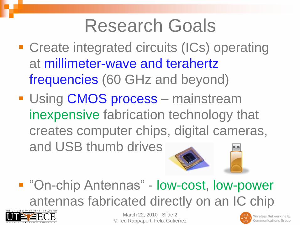
Create integrated circuits (ICs) operating
at millimeter-wave and terahertz
frequencies (60 GHz and beyond)
Using CMOS process – mainstream
inexpensive fabrication technology that
creates computer chips, digital cameras,
and USB thumb drives
“On-chip Antennas” - low-cost, low-power
antennas fabricated directly on an IC chipMarch 22, 2010 - Slide 2
© Ted Rappaport, Felix Gutierrez
Research Goals

April 23, 2010 – Slide 3
© Ted Rappaport, Felix Gutierrez
Why mmWave? Huge amounts of wireless spectrum available (currently unused)
Able to send massive amounts of data (billions of bits every second)
over local area (~10 meters)
Directionality in sensing – vehicle radar
Inexpensive CMOS fabrication now capable of mmWave operation
Contains 2 antennas
mmWave antenna sizes are
comparable to integrated circuit (IC)
sizes
Tiny metal sheets available on ICs
to fabricate mmWave/THz antennas
Reduces fabrication costs
Low power, light weight,
won’t vibrate loose.

March 22, 2010 - Slide 4
© Ted Rappaport, Felix Gutierrez
• Spectrum = real estateAM Radio
FM Radio
TV Broadcast
Wi-Fi
60GHz
Spectrum
Cellular
Shaded Areas =
Equivalent
Spectrum!
77GHz
Vehicular
Radar
Active
CMOS IC
Research

March 22, 2010 - Slide 5
© Ted Rappaport, Felix Gutierrez
Applications - Vehicle Radar
Phased array of IC antennas
Directional beam for long distance vehicle radar and collision avoidance
Steerable beams

April 23, 2010 – Slide 6
© Ted Rappaport, Felix Gutierrez
10010110101001011010100101
10101001011010100101101010
10110110010110110010110110
01011010100101101010010110
10100101101010010110101010
11011001010010110101001011
01010010110101001011010100
10110101010110101101010110
10101101010110101011010101
101010110101011010101101
100101101010010110101
001011010100101101010
010110101010110110010
1101100101101
100101101010010110101
001011010100101101010
010110101010110110010
100101101010010110101
001011010100101101010
010110101010110110010
1101100101101
1101100101101
Information Showers The future: Showering
of information
Mounted on ceilings,
walls, doorways,
roadside
Massive data streaming
while walking or driving
Roadside markers can
provide safety
information, navigation,
or even ads
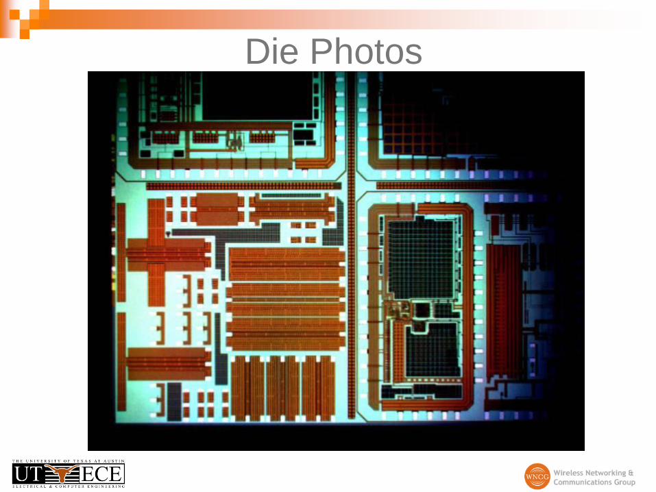
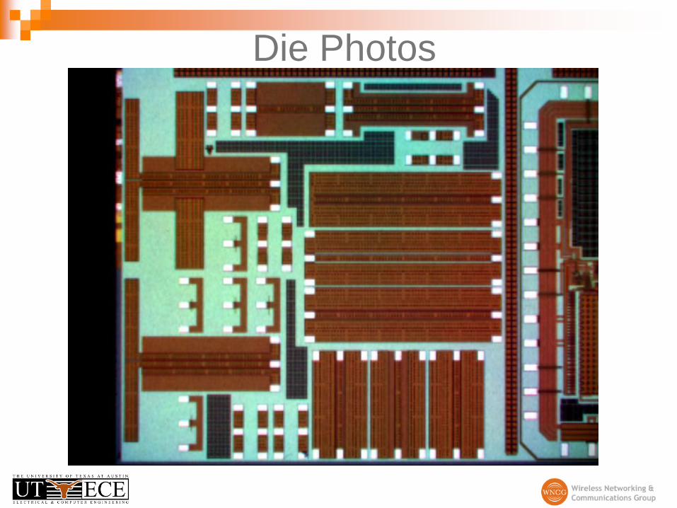
Die Photos

Die Photos

Objective of This Presentation
Provide tips and precautions for creating
on-chip antennas at mmWave
Common tools used to help create on-chip
antennas at mmWave
Show an example CMOS integrated circuit
(IC) created at UT-Austin
Contains 2 on-chip mmWave antennas and
an array of test structures to help design and
simulate on-chip antennas
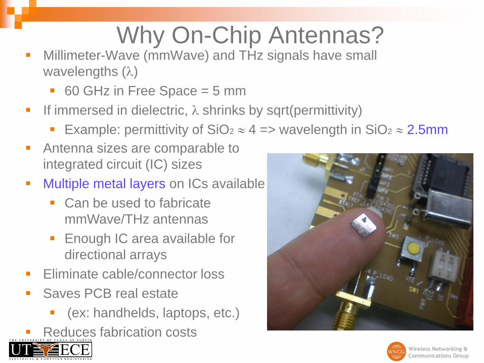
Why On-Chip Antennas? Millimeter-Wave (mmWave) and THz signals have small
wavelengths ( )
60 GHz in Free Space = 5 mm
If immersed in dielectric, shrinks by sqrt(permittivity)
Example: permittivity of SiO2 4 => wavelength in SiO2 2.5mm
Antenna sizes are comparable to
integrated circuit (IC) sizes
Multiple metal layers on ICs available
Can be used to fabricate
mmWave/THz antennas
Enough IC area available for
directional arrays
Eliminate cable/connector loss
Saves PCB real estate
(ex: handhelds, laptops, etc.)
Reduces fabrication costs
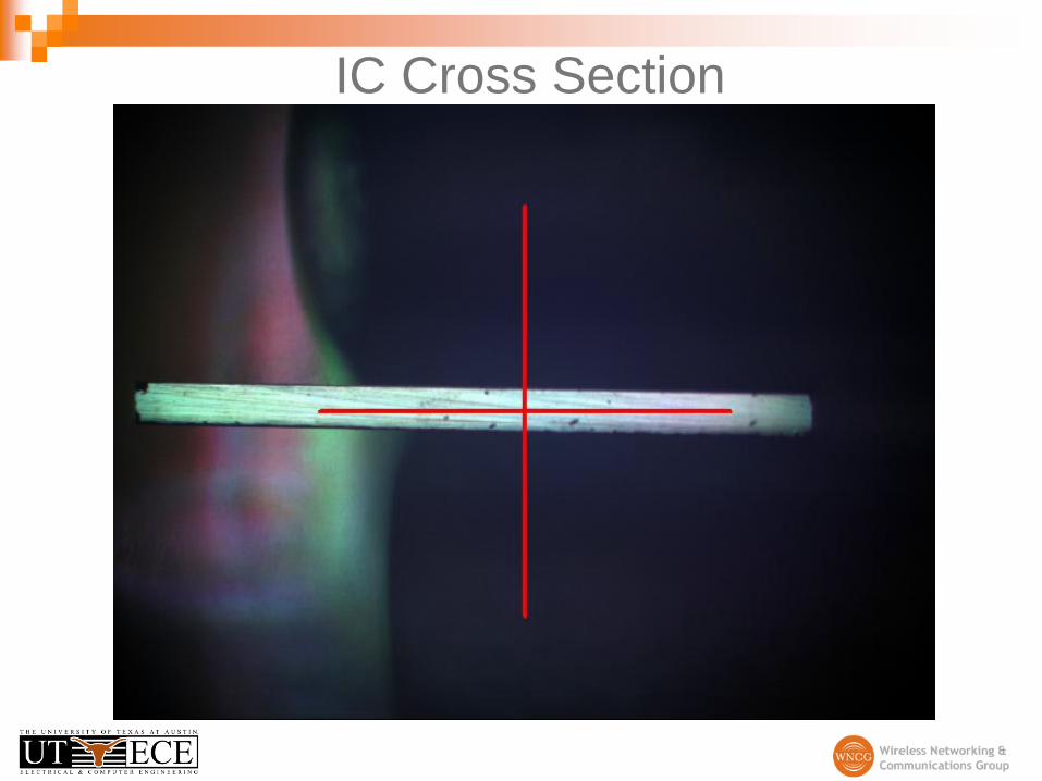
IC Cross Section

IC Cross Section
Metal Layers 10 m Substrate 100 - 750 m
Bulk Silicon
10 m
300 m

Metal Layers 10 m
“Interconnect”
“BEOL”
IC Cross Section
“Diffusion” Layer 1 m
Substrate 100 - 750 m
Bulk Silicon
“FEOL”
10 m

Silicon Substrate
“Length”
Ex: 180, 90, 45 nmSource Drain
GateEx: Polysilicon, Metal
InsulatorEx: SiO2, High-k
DS
G
Transistor Cross Section
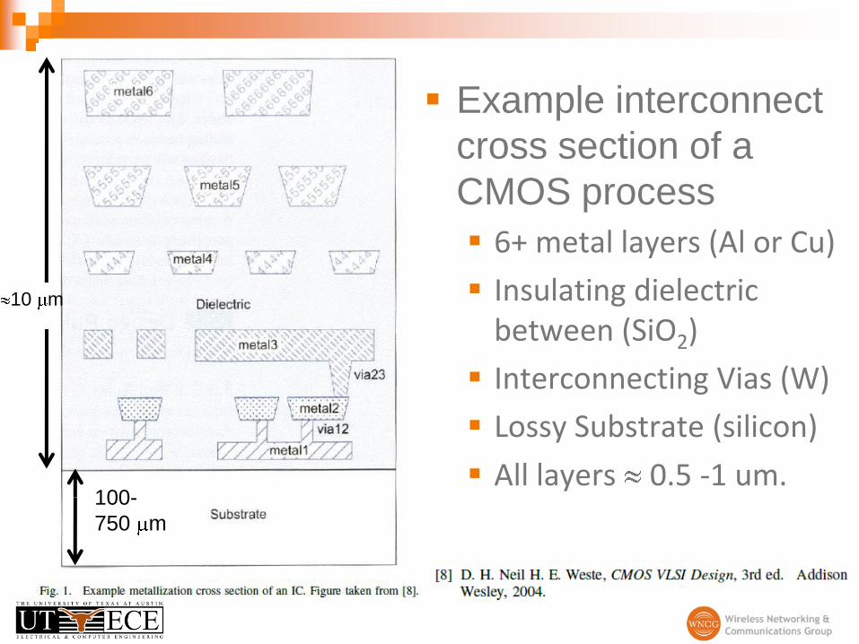
Example interconnect
cross section of a
CMOS process
6+ metal layers (Al or Cu)
Insulating dielectric between (SiO2)
Interconnecting Vias (W)
Lossy Substrate (silicon)
All layers 0.5 -1 um.
10 m
100-
750 m

Transistors buried in substrate
(1 m deep)
Metal layers/vias used to
interconnect transistors
In Analog/RF, can also be used to create passive structures such as parallel plate capacitors (ex: Metal-Insulator-Metal “MIM” Caps) or inductor loops
10 m
100-
750 m

Thicker Metal Layers
at top
Likely used for power
lines and antenna
fabrication
Rectangular vias with
variable sizes across layers
10 m
100-
750 m

Each IC generation
packs more layers of
metal
9 metal layers in 45nm technology
Push towards “low-k” dielectric for digital circuits
Permittivity of dielectric approaching 2
10 m
100-
750 m

Very thick top metal
layer
Denoted as “+1” such as “7+1”
Passivation layer
placed above top-
most metal layer (not
shown)
Protects chip from environment
10 m
100-
750 m

mmWave RFIC Fabrication
Designing and fabricating RFICs and antennas
requires extensive use of electromagnetic
simulators Electrical properties of materials are needed to accurately
simulate electric and magnetic fields
Losses can significantly alter radiation patterns and performance
such as radiation efficiency
Electromagnetic simulators require Relative permittivity ( r) of all insulators
Conductivity ( ) of metal layers and loss tangent ( ) of insulators
Thickness and sometimes surface roughness of metal layers
Substrate (silicon) conductivity and losses

Materials properties such as metal
conductivities and dielectric losses are
frequency dependent and unknown at
mmWave and terahertz regime Foundry may not know, especially older fab
technology
Materials are also process dependent as
metal thicknesses shrink and dielectric
properties change (ex: low-k dielectrics)
each generation
Can change wafer to wafer

EMAG Simulators
Finite Element Method
(FEM) - can be used for
planar and 3-D objects
Moment method (MOM) -
mainly used for planar
structures
Finite Difference Time
Domain (FDTD) - time-
domain calculation and
representation of fields
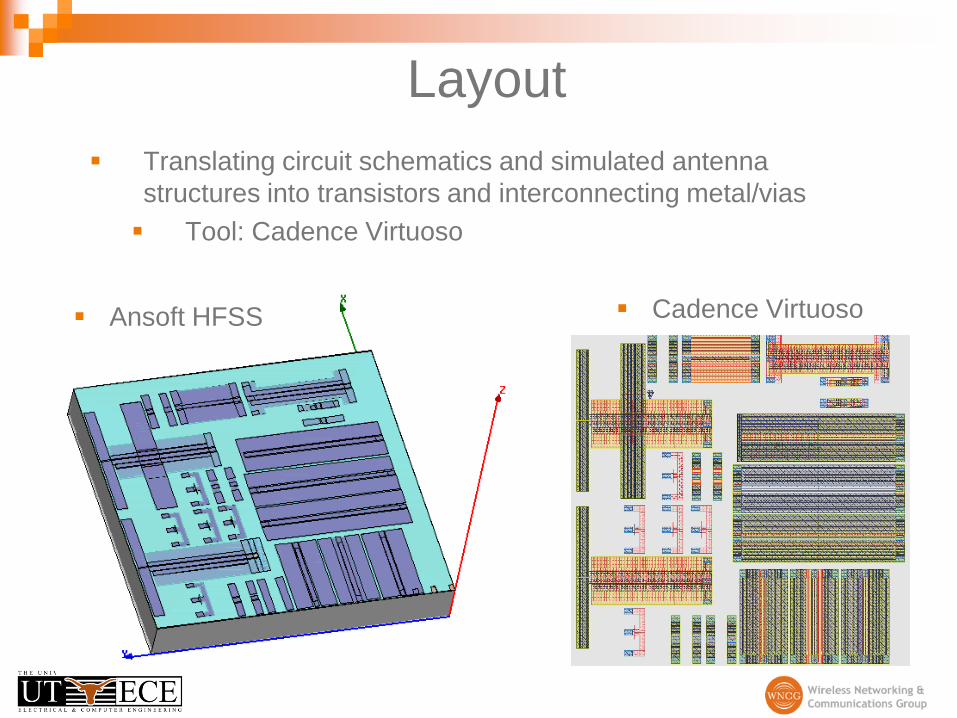
Layout
Translating circuit schematics and simulated antenna
structures into transistors and interconnecting metal/vias
Tool: Cadence Virtuoso
Ansoft HFSS Cadence Virtuoso

Foundry Layout Constraints
Foundry will provide a “process design kit” (PDK)
Contains materials used, thicknesses, and “design
rules”
Design Rules ensure layout is fabrication-compatible
Ex: Min/Max spacing of co-planar metal lines or transistors
Provides protection for your chip and for neighboring chips
Important to perform Design Rules Check (DRC) before
submitting layout to foundry
DRC be done with Mentor’s Calibre and integrated with Virtuoso
DRC dictates antenna/RF designs
Some design rule errors can be “waived”
Re-simulation may be necessary!

Layout vs. Schematic (LVS)
Simply passing DRC is not enough
DRC only guarantees foundry can fabricate the chip,
however unknown whether chip will perform as
intended
Layout vs. Schematic (LVS) performs checks
between layout and circuit schematic Helps identify missed connections, short/open circuits, etc.
LVS can be performed with Mentor’s Calibre and integrated into
Virtuoso
Passing both DRC and LVS provides confidence
for proper layout and successful tape-out

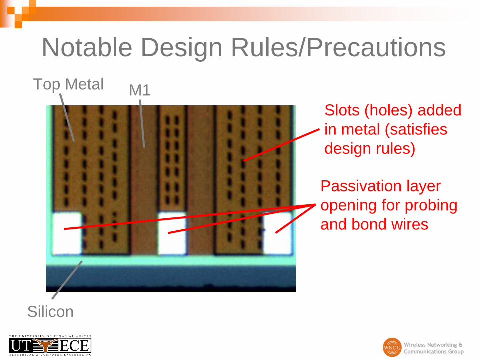
Notable Design Rules/Precautions
Designer must know foundry constraints
Metal-Percentage Rule
Each metal layer must occupy a minimum percentage of entire
design area
Ex: At least 35% of IC area (max width*max length) must
contain M1, M2, M3, etc.
Wide-Metal Rule
If a metal area is larger/wider than a threshold, small slots
(holes) must be inserted
Ex: If M1 occupies an area 50 m x 50 m, then a small slot
of at least 10 m2 will need to be placed in that area. The
slot density must be at least 3%.
Notable Design Rules/Precautions
Pads either for probing or bond wires will require as many metal
layers as possible with stacked vias for mechanical stability.
Probe manufacturers may have additional rules for pad creation
Ex: Pad sizes and placement for successful probing
Smaller pad sizes = less parasitic capacitance = easier to de-
embed parasitic from device under test (DUT)
Pad rings located around the perimeter of the chip may alter antenna
designs/patterns
Scribe lines located beyond the pad rings may also alter antenna
performance
Notable Design Rules/Precautions
Slots (holes) added
in metal (satisfies
design rules)
Passivation layer
opening for probing
and bond wires
Top Metal M1
Silicon

Notable Design Rules/Precautions
Pad Ring
Scribe Line
MIM Caps to
satisfy design
rules

5mm
5mm
Collaborative die among several faculty/students
6 Projects on 5mm x 5mm
Includes UT’s first ever on-chip 60 GHz antennas!
Our quadrant – 2.5mm x 2.5mm
Example Layout at UT-Austin

Example Layout at UT-Austin
Contains 2 on-chip antennas for 60GHz operation
Publication in IEEE JSAC Oct. 2009
An array of transmission lines (CPW/MS) used for measurement and fine tuning of simulation parameters @ mmWave/THz (ex: r
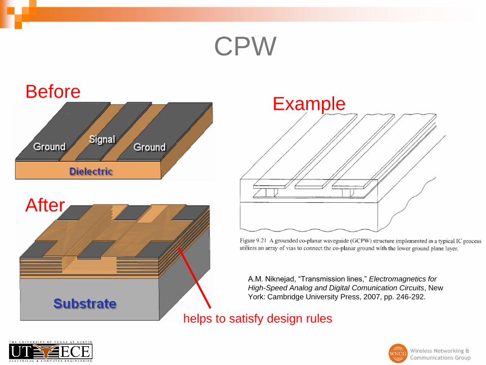
CPW
A.M. Niknejad, “Transmission lines,” Electromagnetics for
High-Speed Analog and Digital Comunication Circuits, New
York: Cambridge University Press, 2007, pp. 246-292.
Before
After
Example
helps to satisfy design rules

Die Photos
Die Photos
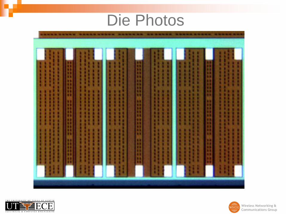
Die Photos

Die Photos
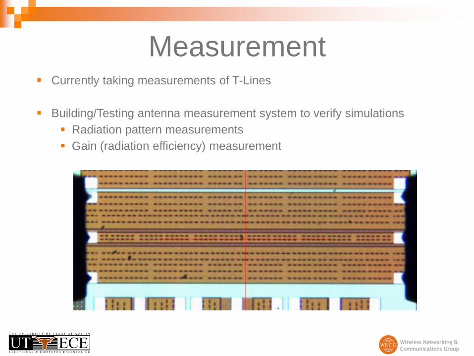
Measurement Currently taking measurements of T-Lines
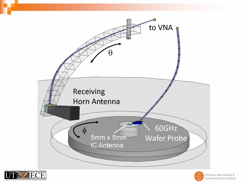
Building/Testing antenna measurement system to verify simulations
Radiation pattern measurements
Gain (radiation efficiency) measurement
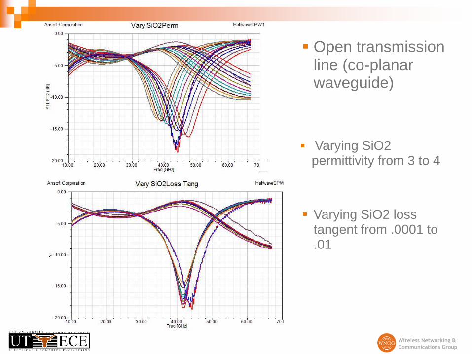
Varying SiO2 permittivity from 3 to 4
Varying SiO2 loss tangent from .0001 to .01
Open transmission line (co-planar waveguide)

Direct Probing of T-Lines
Cascade Microtech 67GHz Probes
Ground-Signal-Ground (GSG)
300um

© Felix Gutierrez, Ted
Rappaport
Optimized Dipole Antenna
F. Gutierrez, K. Parrish, T. S. Rappaport, “On-Chip Integrated Antenna
Structures in CMOS for 60 GHz WPAN Systems,” IEEE Journal on Selected
Areas in Communications. (Accepted for publication in 4th quarter 2009)
© Felix Gutierrez, Ted
Rappaport
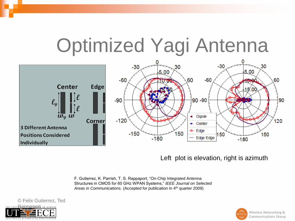
Optimized Yagi Antenna
F. Gutierrez, K. Parrish, T. S. Rappaport, “On-Chip Integrated Antenna
Structures in CMOS for 60 GHz WPAN Systems,” IEEE Journal on Selected
Areas in Communications. (Accepted for publication in 4th quarter 2009)
Left plot is elevation, right is azimuth

Conclusion Tremendous spectrum available at
millimeter-wave/terahertz radio
frequencies
Emerging low-cost, low-power mainstream
CMOS fabrication
Need to understand: circuits and antennas
Applications are numerous: vehicular
radar, short-range high-speed data
transfers
April 23, 2010 – Slide 44
© Ted Rappaport, Felix Gutierrez
Conclusion
Electromagnetic simulators require accurate frequency dependent materials to design mmWave RFICs
Design rules and foundry constraints should be checked regularly during the design process
UT-Austin’s Wireless Networking and Communications Group is actively researching mmWave RFICs

References
April 23, 2010 – Slide 46
© Ted Rappaport, Felix Gutierrez
Gutierrez, F.; Agarwal, S.; Parrish, K.; Rappaport, T.S., "On-chip integrated
antenna structures in CMOS for 60 GHz WPAN systems," Selected Areas
in Communications, IEEE Journal on , vol.27, no.8, pp.1367-1378,
October 2009.
Rappaport, Theodore S.; Gutierrez Jr., Felix; Al-Attar, Talal, "Millimeter-
Wave and Terahertz Wireless RFIC and On-Chip Antenna Design: Tools
and Layout Techniques," GLOBECOM Workshop on Multi-Gigabit mm-
Wave and Tera-Hz Wireless Systems (MWTS), 2009 IEEE, vol., no., pp.1-
7, Nov. 30 2009-Dec. 4 2009.
L. Ragan, A. Hassibi, T. S. Rappaport, C. L. Christianson, “Novel On-Chip
Antenna Structures and Frequency Selective Surface (FSS) Approaches
for Millimeter Wave Devices,” IEEE 66th Vehicular Technology Conference
(VTC), Baltimore, MD, Oct. 1-3, 2007, pp. 2051-2055.
C. H. Park, T. S. Rappaport, “Short-Range Wireless Communications for
Next-Generation Networks: UWB, 60 GHz Millimeter Wave PAN, and
Zigbee,” IEEE Wireless Communications Magazine, Vol. 14, Issue 4,
August 2007, pp. 70-78.
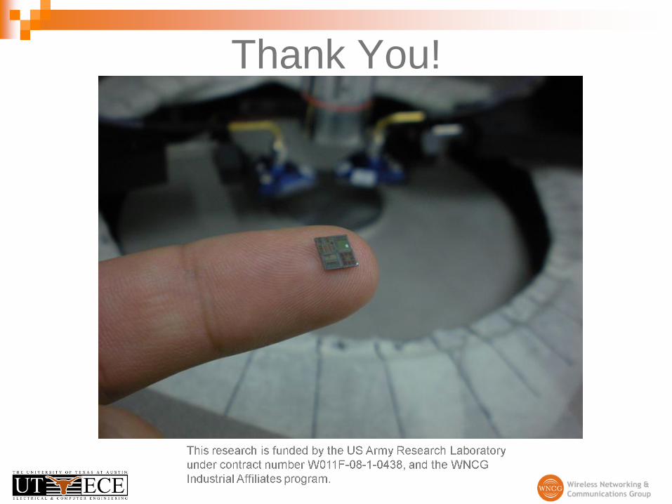
Thank You!
Related Documents


