Eclipse Series RF Technology [email protected] February 2005 R350/R500 Receiver Operation and Maintenance Manual This manual is produced by RF Technology Pty Ltd 10/8 Leighton Place, Hornsby, 2077 NSW Australia Copyright ©1998, RF Technology

Welcome message from author
This document is posted to help you gain knowledge. Please leave a comment to let me know what you think about it! Share it to your friends and learn new things together.
Transcript
Eclipse Series
RF Technology [email protected]
February 2005
R350/R500 Receiver Operation and Maintenance Manual
This manual is produced by RF Technology Pty Ltd 10/8 Leighton Place, Hornsby, 2077 NSW Australia
Copyright ©1998, RF Technology
Page 2 RF Technology R350/R500
CONTENTS CONTENTS
Contents 1 Operating Instructions 5 1.1 Front Panel Controls and Indicators 5 1.1.1 Mon. Volume 5 1.1.2 Mon. Sq. 5 1.1.3 N. SQ 5 1.1.4 C. SQ 6 1.1.5 Line 6 1.1.6 Power LED 6 1.1.7 SQ LED 6 1.1.8 Alarm LED 6 2 Receiver Internal Jumper Options 7 2.1 JP1: 240Hz Notch Filter 7 2.2 JP2: Audio Response 7 2.3 JP3: Audio Filter In/Out 8 2.4 JP4: 600Ω Line dc Loop COS 8 2.5 JP6: COS Polarity 8 2.6 JP7, JP8, JP9: dc Loop COS Configuration 8 2.7 JP7, JP8, JP9: Direct Output COS 9 2.8 JP11 EPROM Type 9
2.9 JP13: Squelch Defeat (pcb 30/9131/0004 or later) 9 2.10 JP19: LED Alarm output (pcb 30/9131/0004 or later) 9
3 Receiver I/O Connections 9 3.1 25 Pin Connector 9 4 Frequency Programming 9 5 Circuit Description 11 5.1 RF Section 11 5.2 IF Section 11 5.3 VCO Section 12 5.4 PLL Section 12 5.5 Audio Signal Processing 13 5.6 Noise Filter, Amplifier and Detector 13 5.7 Subtone Filter and CTCSS 13 5.8 Microprocessor Controller 14 5.9 Carrier Operated Switch 14 5.10 Voltage Regulator 14 6 Alignment Procedure 14 6.1 Standard Input Signal 15 6.2 RF Alignment 15 6.3 IF Alignment 15 6.4 Line Level Adjustment 16 6.5 TCXO Calibration 16
RF Technology R350/R500 Page 3
CONTENTS CONTENTS 7 Specifications 16 7.1 General Description 16 7.1.1 Channel Capacity 16 7.1.2 CTCSS 16 7.1.3 Channel Programming 17 7.1.4 Channel Selection 17 7.1.5 Microprocessor 17 7.2 Physical Configuration 17 7.3 Front Panel Controls, Indicators and Test Points 17 7.3.1 Controls 17 7.3.2 Indicators 18 7.3.3 Test Points 18 7.4 Electrical Specifications 18 7.4.1 Power Requirements 18 7.4.2 Frequency Range and channel Spacing 18 7.4.3 Frequency Synthesizer Step Size 19 7.4.4 Frequency Stability 19 7.4.5 Nominal Antenna Impedance 19 7.4.6 IF Frequencies 19 7.4.7 Sensitivity 19 7.4.8 Selectivity 19 7.4.9 Spurious and Image Rejection 19 7.4.10 Intermodulation 19 7.4.11 Modulation Acceptance BW 20 7.4.12 Noise Squelch 20 7.4.13 Carrier Level Squelch 20 7.4.14 Receiver Frequency Spread for -1dB Degradation 20 7.4.15 Receiver Conducted Spurious Emissions 20 7.4.16 Audio Frequency Response 20 7.4.17 Audio Output Level 20 7.4.18 Audio Distortion 21 7.4.19 Channel Select Input / Output 21 7.4.20 Carrier Operated Switch Output 21 7.4.21 CTCSS 21 7.4.22 External Squelch Input 23 7.5 Connectors 23 7.5.1 Antenna Connector 23 7.5.2 Power and I/O Connector 23 7.5.3 Test Connector 23 A Engineering Diagrams 23 A.1 Block Diagram 23 A.2 Component Overlay Diagram 23 A.3 Jumper Link Positions 23 A.4 Jumper Link Description 23 B Parts List 27
Page 4 RF Technology R350/R500
1 OPERATING INSTRUCTIONS
WARNING Changes or modifications not expressly approved by RF Technology could void your authority to operate this equipment. Specifications may vary from those given in this document in accordance with requirements of local authorities. RF Technology equipment is subject to continual improvement and RF Technology reserves the right to change performance and specification without further notice.
1 Operating Instructions 1.1 Front Panel Controls and Indicators 1.1.1 Mon. Volume The Mon. Volume control is used to adjust the volume of the internal loudspeaker and any external speaker connected to the test socket. It does not effect the level of the 600Ω line or direct audio output. 1.1.2 Mon. SQ. The Mon. Sq. switch allows all squelch functions controlling the monitor output to be disabled. This can be useful when you are trying to trace the source of on-channel interference. 1.1.3 N.SQ The N.SQ trimpot is used to set the noise squelch sensitivity. Use the following procedure to set the noise squelch to maximum sensitivity. 1. Turn the adjustment counter clockwise until the squelch opens as indicated by
the SQ LED. 2. In the absence of any on channel signal, turn the screw clockwise until the SQ
LED goes off. Then turn the screw one additional turn in the clockwise direction.
RF Technology R350/R500 Page 5
1.1 Front Panel Controls and Indicators 1 OPERATING INSTRUCTIONS 1.1.4 C.SQ The C.SQ trimpot is used to set the carrier squelch sensitivity. Carrier squelch is useful at higher signal levels than those at which noise squelch can be used – typically from 1-200µ V input. It is provided mainly for use in fixed link applications where a high minimum signal to noise ratio is required or where very fast squelch operation is required for data transmission. The carrier squelch will open and close in less than 2~ms. In most base station applications carrier squelch is disabled by turning the adjustment counter clockwise. The carrier squelch may be set to a predetermined level as follows:
1. First turn the adjustment fully counter-clockwise. Then set the noise squelch as above. 2. Connect a source of an on channel signal with the desired threshold level to
the receiver's RF input. 2. Turn the screw clockwise until the SQ LED goes OFF. Then turn the screw back until the LED just comes ON.
1.1.5 LINE The LINE trimpot is used to set the line and direct audio output level. It is normally set so that 0dBm (775mV) with a standard input signal gives 60% of maximum deviation at 1 KHz. The level can be measured between test socket pins 6 and 1 and set as desired. 1.1.6 POWER LED The Power LED shows that the dc supply is connected to the receiver. 1.1.7 SQ LED The SQ LED comes on when the audio to the line and direct outputs is unsquelched. The LED and squelch function are controlled by noise, carrier and tone squelch circuits. 1.1.8 ALARM LED The Alarm LED can indicate the detection of several different fault conditions by the self test circuits. The alarm indicator shows the highest priority fault present. Receivers using software issue 5 and higher use the cadence of the LED flash sequence to indicate the alarm condition. Refer to table 1. Receivers using software
Page 6 RF Technology R350/R500
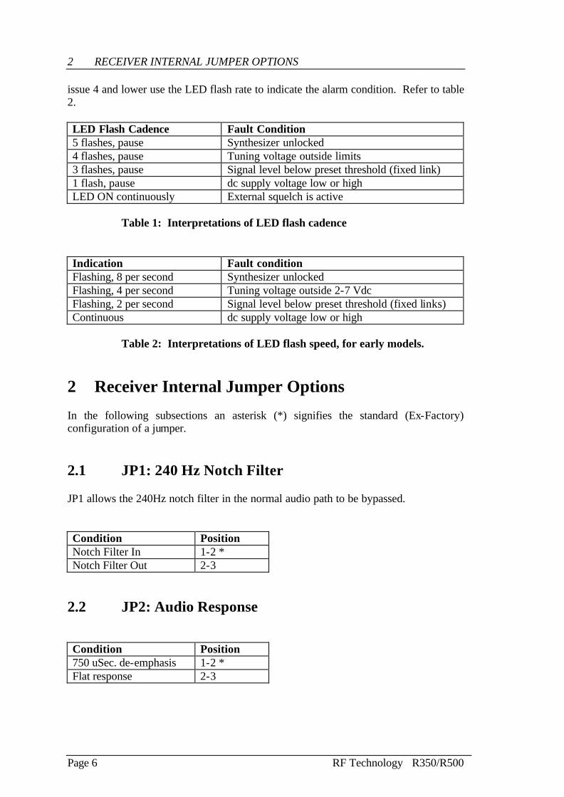
2 RECEIVER INTERNAL JUMPER OPTIONS issue 4 and lower use the LED flash rate to indicate the alarm condition. Refer to table 2. LED Flash Cadence Fault Condition 5 flashes, pause Synthesizer unlocked 4 flashes, pause Tuning voltage outside limits 3 flashes, pause Signal level below preset threshold (fixed link) 1 flash, pause dc supply voltage low or high LED ON continuously External squelch is active
Table 1: Interpretations of LED flash cadence Indication Fault condition Flashing, 8 per second Synthesizer unlocked Flashing, 4 per second Tuning voltage outside 2-7 Vdc Flashing, 2 per second Signal level below preset threshold (fixed links) Continuous dc supply voltage low or high
Table 2: Interpretations of LED flash speed, for early models.
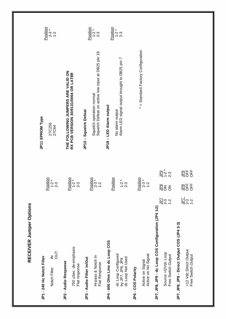
2 Receiver Internal Jumper Options In the following subsections an asterisk (*) signifies the standard (Ex-Factory) configuration of a jumper. 2.1 JP1: 240 Hz Notch Filter JP1 allows the 240Hz notch filter in the normal audio path to be bypassed. Condition Position Notch Filter In 1-2 * Notch Filter Out 2-3
2.2 JP2: Audio Response Condition Position 750 uSec. de-emphasis 1-2 * Flat response 2-3
RF Technology R350/R500 Page 7
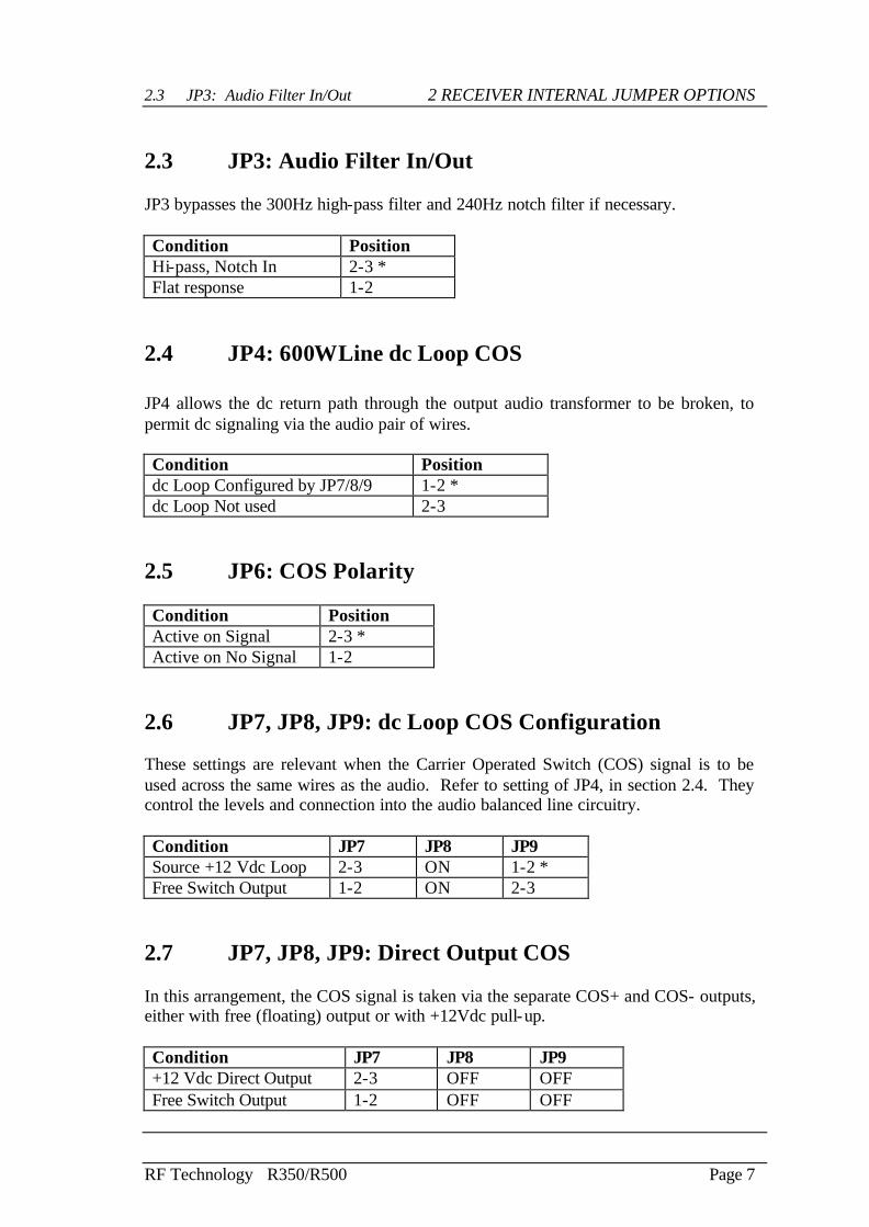
2.3 JP3: Audio Filter In/Out 2 RECEIVER INTERNAL JUMPER OPTIONS 2.3 JP3: Audio Filter In/Out JP3 bypasses the 300Hz high-pass filter and 240Hz notch filter if necessary. Condition Position Hi-pass, Notch In 2-3 * Flat response 1-2
2.4 JP4: 600Ω Line dc Loop COS JP4 allows the dc return path through the output audio transformer to be broken, to permit dc signaling via the audio pair of wires. Condition Position dc Loop Configured by JP7/8/9 1-2 * dc Loop Not used 2-3
2.5 JP6: COS Polarity Condition Position Active on Signal 2-3 * Active on No Signal 1-2
2.6 JP7, JP8, JP9: dc Loop COS Configuration These settings are relevant when the Carrier Operated Switch (COS) signal is to be used across the same wires as the audio. Refer to setting of JP4, in section 2.4. They control the levels and connection into the audio balanced line circuitry. Condition JP7 JP8 JP9 Source +12 Vdc Loop 2-3 ON 1-2 * Free Switch Output 1-2 ON 2-3
2.7 JP7, JP8, JP9: Direct Output COS In this arrangement, the COS signal is taken via the separate COS+ and COS- outputs, either with free (floating) output or with +12Vdc pull-up. Condition JP7 JP8 JP9 +12 Vdc Direct Output 2-3 OFF OFF Free Switch Output 1-2 OFF OFF
Page 8 RF Technology R350/R500
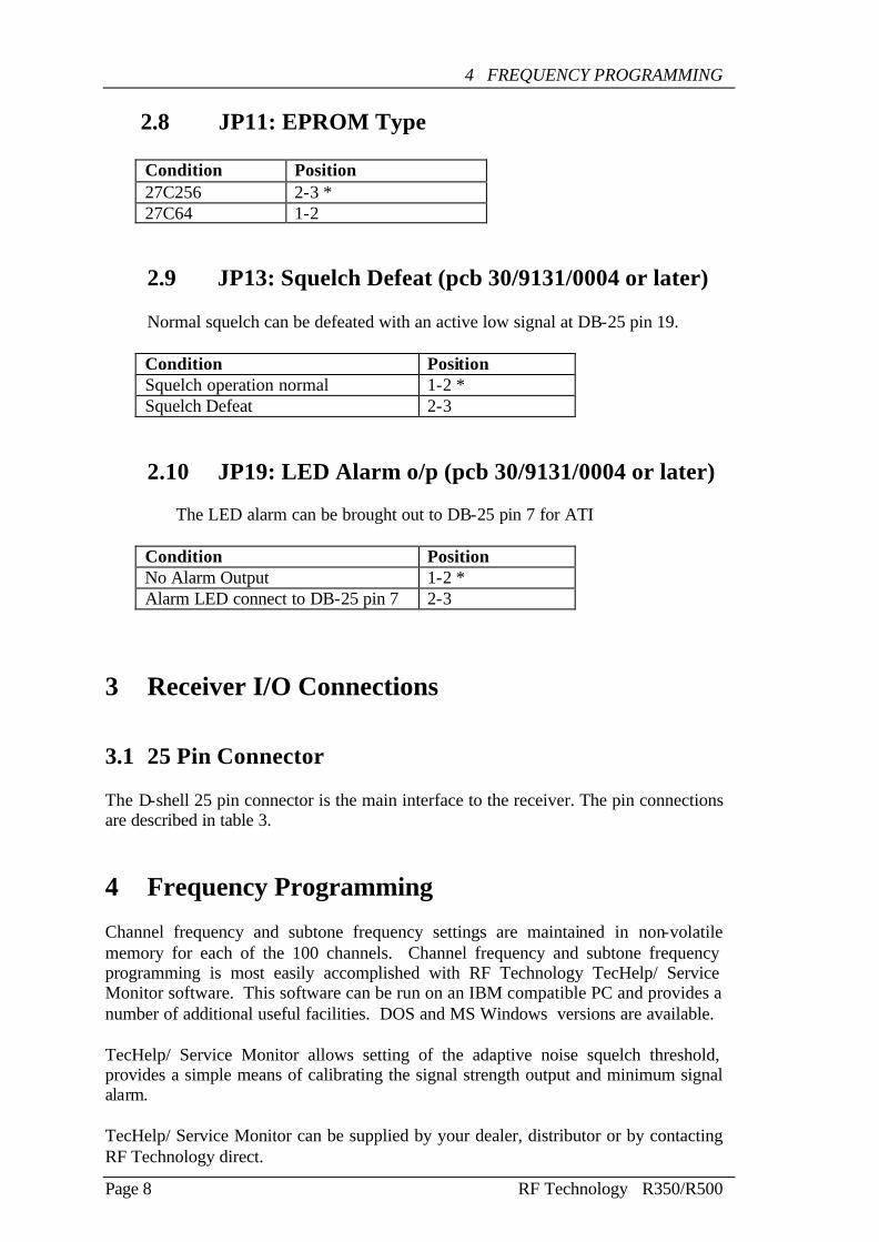
4 FREQUENCY PROGRAMMING 2.8 JP11: EPROM Type
Condition Position 27C256 2-3 * 27C64 1-2
2.9 JP13: Squelch Defeat (pcb 30/9131/0004 or later)
Normal squelch can be defeated with an active low signal at DB-25 pin 19. Condition Position Squelch operation normal 1-2 * Squelch Defeat 2-3
2.10 JP19: LED Alarm o/p (pcb 30/9131/0004 or later) The LED alarm can be brought out to DB-25 pin 7 for ATI
Condition Position No Alarm Output 1-2 * Alarm LED connect to DB-25 pin 7 2-3
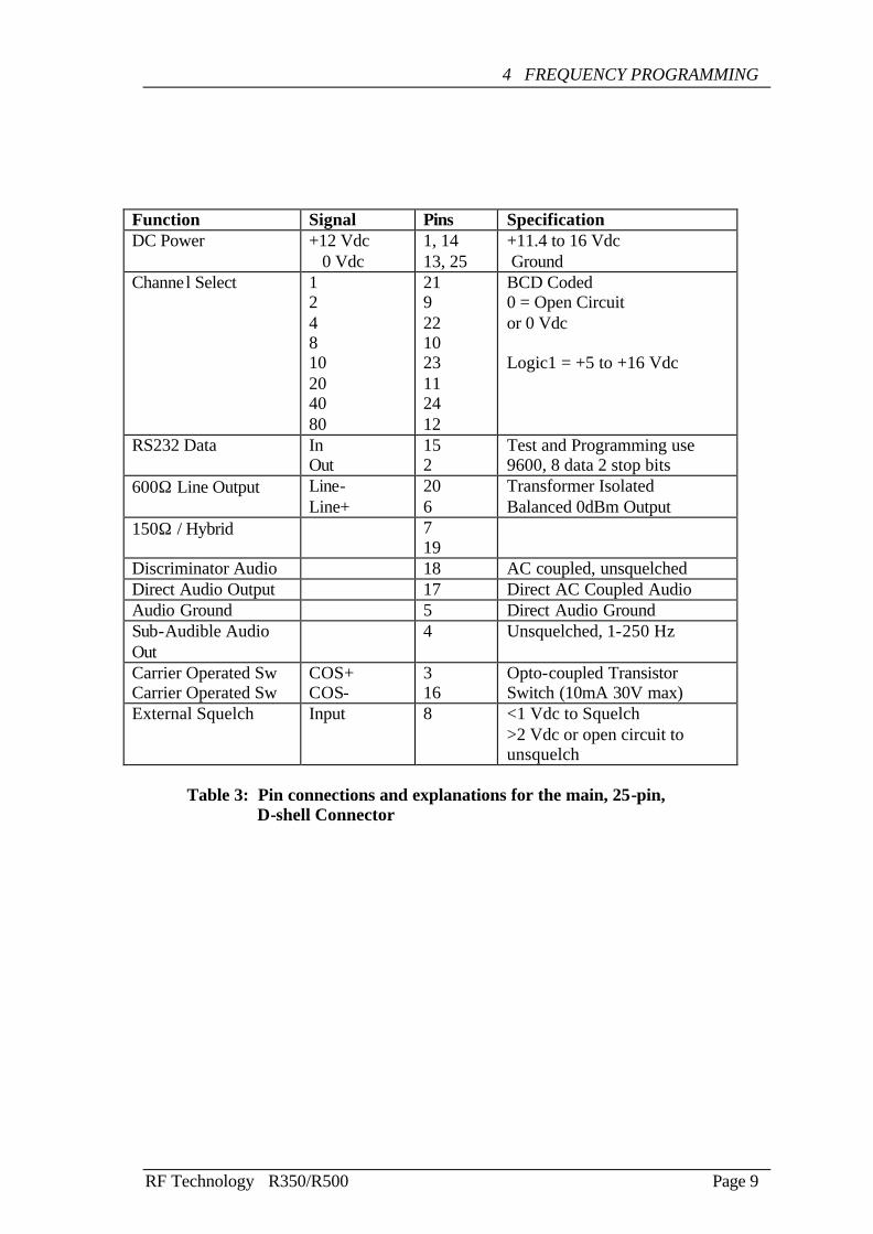
3 Receiver I/O Connections 3.1 25 Pin Connector The D-shell 25 pin connector is the main interface to the receiver. The pin connections are described in table 3.
4 Frequency Programming Channel frequency and subtone frequency settings are maintained in non-volatile memory for each of the 100 channels. Channel frequency and subtone frequency programming is most easily accomplished with RF Technology TecHelp/ Service Monitor software. This software can be run on an IBM compatible PC and provides a number of additional useful facilities. DOS and MS Windows versions are available. TecHelp/ Service Monitor allows setting of the adaptive noise squelch threshold, provides a simple means of calibrating the signal strength output and minimum signal alarm. TecHelp/ Service Monitor can be supplied by your dealer, distributor or by contacting RF Technology direct.
RF Technology R350/R500 Page 9
4 FREQUENCY PROGRAMMING
Function Signal Pins Specification DC Power +12 Vdc
0 Vdc 1, 14 13, 25
+11.4 to 16 Vdc Ground
Channel Select 1 2 4 8 10 20 40 80
21 9 22 10 23 11 24 12
BCD Coded 0 = Open Circuit or 0 Vdc Logic1 = +5 to +16 Vdc
RS232 Data In Out
15 2
Test and Programming use 9600, 8 data 2 stop bits
600Ω Line Output Line- Line+
20 6
Transformer Isolated Balanced 0dBm Output
150Ω / Hybrid 7 19
Discriminator Audio 18 AC coupled, unsquelched Direct Audio Output 17 Direct AC Coupled Audio Audio Ground 5 Direct Audio Ground Sub-Audible Audio Out
4 Unsquelched, 1-250 Hz
Carrier Operated Sw Carrier Operated Sw
COS+ COS-
3 16
Opto-coupled Transistor Switch (10mA 30V max)
External Squelch Input 8 <1 Vdc to Squelch >2 Vdc or open circuit to unsquelch
Table 3: Pin connections and explanations for the main, 25-pin, D-shell Connector
Page 10 RF Technology R350/R500
5 CIRCUIT DESCRIPTION 5.1 RF Section
5 Circuit Description The following descriptions should be read as an aid to understanding the block and schematic diagrams at the rear of this manual. 5.1 RF Section A two section helical filter FL1 is used to limit the RF band width prior to the RF amplifier transistor Q1. The output impedance of FL1 is matched to the input of Q1 by C165, C1 and a microstrip line on the printed circuit board. Q1 is a very low noise device with good intermodulation performance. A four section filter consisting of FL2 and FL3 is used between Q1 and the mixer MX1. This filter provides additional image and spurious frequency rejection. The gain between the receiver input and the mixer input is approximately 10dB. Monolithic amplifiers MA1, MA2 and transistor Q5 amplify the VCO output to the necessary LO level for MX1. MX1 is a high dynamic range double balanced mixer. The LO input level to MX1 is approximately +13dBm the mixer conversion gain is approximately -7dB. The network C7, C9, L1, L3 and R7 passes the IF frequency of 45 MHz and terminates the RF and LO components. The total RF section gain from J1 to the IF input is approximately 3dB. 5.2 IF Section The first IF amplifier uses two parallel connected JFET transistors Q2 and Q3 to obtain 12-15dB gain. The two transistors provide improved dynamic range and input matching over a single transistor. A two pole 45 MHz crystal filter XF1 is used between the first and second IF amplifiers. The second IF amplifier Q4 provides additional gain of 6-10dB. A two pole crystal filter is used between Q4 and the 2nd oscillator mixer. These two crystal filters provide some adjacent channel rejection and all of the second IF image frequency rejection. U1 is a monolithic oscillator and mixer IC It converts the 45 MHz IF signal down to 455 kHz. The second oscillator frequency or 45.455 MHz is controlled by crystal Y1. The 455 kHz output of the second mixer is fed through a ceramic filter CF1 to the limiter and discriminator IC U3. CF1 provides additional adjacent channel selectivity for 25 kHz versions and all of the adjacent channel selectivity for 12.5 kHz versions.
RF Technology R350/R500 Page 11
5.3 VCO Section 5 CIRCUIT DESCRIPTION CF1 and its termination resistors R15 and R24 are the only component differences in the two versions. The limiter/discriminator IC U3 further amplifies the signal and passes it through CF2. CF2 does not contribute to the adjacent channel rejection but is used to reduce the wide band noise input to the limiter section of U3. The limiter section of U3 drives the quadrature detector discriminator. C31 and IF tuned circuit L10 comprise the discriminator phase shift network. U3 also has a received signal strength indicator output (RSSI). The RSSI voltage connects to the test socket for alignment use. The RSSI voltage is also used by the microprocessor for the adaptive noise squelch, carrier squelch and low signal alarm functions. Dual op-amp U2 is used to amplify and buffer the discriminator audio and RSSI outputs. 5.3 VCO Section The Voltage Controlled Oscillator uses a junction FET Q6 which oscillates at the required mixer injection frequency. Varactor diode D4 is used by the PLL circuit to keep the oscillator on the desired frequency. Transistor Q7 is used as a filter to reduce the noise on the oscillator supply voltage. 5.4 PLL Section Temperature compensated crystal oscillator XO1 is the frequency reference source for the PLL Synthesizer. The frequency stability of XO1 is better than 1 ppm. The 12.8 MHz output of XO1 is amplified by Q8 to drive the reference input of the PLL synthesizer IC U4. This IC is a single chip synthesizer which includes a 1.1 GHz pre-scaler, programmable divider, reference divider and phase/frequency detector. The frequency data is entered a serial data link from the microprocessor. The phase detector output signals of U4 are used to control two switched current sources. The output of the positive and negative sources' Q10 and Q16, produce the tuning voltage which is smoothed by the loop filter components to bias the VCO varactor diode D4.
Page 12 RF Technology R350/R500
5 CIRCUIT DESCRIPTION 5.5 Audio Signal Processing
5.5 Audio Signal Processing A 4 kHz low pass filter (U27b) is used to remove high frequency noise from the signal. A 300 Hz high pass filter (U26a,b) then removes the sub-audible tones. A 240 Hz notch filter (U26c,d) is used to improve the rejection of tones above 200 Hz. The audio can be set for either 750 uS de-emphasis or a flat response by JP2. JP2 selects the feedback network of amplifier U27c. After de-emphasis and filtering, the audio signal is applied to the inputs of two analog switches (U17a,b). These switches are controlled by the micro-controller and squelch or mute the audio to the line and monitor output circuits. The monitor audio can be unsquelched by S1 which keeps U17a switched on. The audio from U17a is adjusted by the volume control before connecting to the monitor output amplifier U5. U5 drives the internal speaker and can also supply 3-5 watts to an external loudspeaker. The audio from U17b is adjusted by RV3 before connecting to the line output IC (U22a,b). U22 is a dual amplifier connected in a bridge configuration to drive the 600Ω line output transformer T1. 5.6 Noise Filter, Amplifier and Detector The unfiltered audio from the discriminator is fed to trimpot RV4 which is used to set the noise squelch threshold. From RV4 the audio goes to the noise filter (U27a). This is a 10 kHz high pass filter and is used to eliminate voice frequency components. The noise signal is then amplified by U27d and fed to the noise detector. The noise detector consists of D6, Q17 and U26c. D6 and Q17 are a charge pump detector and pull the input to U26c low as the noise increases. U26c has positive feedback and acts like a Schmidt trigger. The output of U26c goes high when noise is detected. It connects to the micro-controller and to analog switch U17d. U17d varies the gain of the noise amplifier to provide approximately 2dB hysteressis. 5.7 Sub-Tone Filter and CTCSS The discriminator audio is fed through cascaded low pass filters U28a and U28b to filter out the voice frequency components. The filtered sub-tone audio is supplied to the CTCSS hybrid and the rear panel system connector. The filtered output can be used for re-transmission of CTCSS or DCS. The CTCSS decoder module is a micro-controller base hybrid module. Under control of the main microprocessor U15 it can decode all 38 EIA tones and 12 additional commonly used tones. The decode bandwidth is set to 1% but may be changed to 2% by a jumper on the printed circuit board.
RF Technology R350/R500 Page 13
5.8 Microprocessor Controller 5 CIRCUIT DESCRIPTION 5.8 Microprocessor Controller The microprocessor controller circuit uses an advanced eight bit processor and several support chips. The processor U15 includes EE memory for channel frequencies, tones, and other information. It also acts as an asynchronous serial port, a synchronous serial port and an analogue to digital converter. The program is stored in U12, a CMOS EPROM. U13 is an address latch for the low order address bits. U11 is used to read the channel select lines onto the data bus. U7 is an address decoder for U11 and U12. U14 is a supervisory chip which keeps the processor reset unless the +5 Volt supply is within operating limits. U16 translates the asynchronous serial port data to standard RS232 levels. The analog to digital converter is used to measure the received signal strength, tuning voltage, dc supply voltage and the carrier squelch setting. 5.9 Carrier Operated Switch The carrier operated switch is an opto-coupled (ISO1) output. Internal jumpers (JP4, JP7, JP8, JP9) can be connected to provide loop source, loop switch, free switch and various other configurations. The COS can be set to be active (switch closed) on carrier or active in the absence of carrier. The generic term ``Carrier Operated Switch'' may be misleading in this case. SINCE, if a sub-audible tone has been programmed for the channel in use, the COS is controlled by carrier and tone detection. 5.10 Voltage Regulator The dc input voltage is regulated down to 9.4 Vdc by a discrete regulator circuit. The series pass transistor Q20 is driven by error amplifiers Q21 and Q22. Q23 is used to start up the regulator and once the circuit turns on, it plays no further part in the operation. This circuit is short circuit and overload protected. It provides much better line isolation and lower dropout voltage than can be obtained with current integrated circuit regulators.
6 Alignment Procedure The following procedures may be used to align the receiver for optimum performance. Normally only RF alignment will be required when changing frequencies. IF alignment should only be necessary after repairs on that part of the circuit.
Page 14 RF Technology R350/R500
6 ALIGNMENT PROCEDURE 6.1 Standard Input Signal TCXO calibration may be required periodically due to crystal aging. The aging should be less than 1 ppm/year. 6.1 Standard Input Signal RF Signal Generator, 50Ω output impedance, Frequency range 350-520MHz, FM modulation at 1kHz, deviation 1.5kHz peak for 12.5KHz channel spacing, 3.0kHz peak for 25kHz channel spacing. 6.2 RF Alignment 1. Select center frequency channel. Measure dc Volts on test socket pin 9 to pin 1.
Adjust C61 to read 4.25 to 4.75V, with Alarm LED off. 2. Set signal generator to the center frequency channel frequency and connect to J1.
Modulation should be off. Measure the dc voltage on the test socket pins 7 to 1. Adjust the generator level to get a reading of 1 - 2Vdc.
3. Set signal generator to the center frequency channel frequency and connect to J1.
Modulation should be off. Measure the dc voltage on the test socket pins 7 to 1. Adjust FL1, FL2, and FL3 for maximum reading, reducing the generator output to keep the voltage below 2Vdc.
6.3 IF Alignment 1. Set signal generator to the center frequency channel frequency and connect to J1.
Modulation should be off. Measure the dc voltage on the test socket pins 7 to 1. Adjust the generator level to get a reading of 1-2Vdc.
2. Set signal generator to the center frequency channel frequency and connect to J1.
Modulation should be off. Measure the dc voltage on the test socket pins 7 to 1. Adjust L5, L6, L7, L8 for maximum reading. Reduce generator output to keep below 2 Vdc.
3. Set generator level to 10µV. Measure the frequency at U3 pin 9, and adjust L9
to obtain a frequency of 455kHz ±10Hz. 4. Set generator level to 1000µV (1mV), and switch the modulation on. Measure
the audio level at the test socket between pins 6 and 1. Adjust the line level (RV3) to obtain approximately 1Vrms.
5. Maintain generator level at 1000µV (1mV), modulation on. Measure the audio level at the test socket between pins 6 and 1. Adjust L10 for maximum reading.
6. Maintain generator level at 1000µV (1mV), modulation on. Measure the audio
level between pins 16 and 5 of P1. Adjust RV1 for 0.5Vrms.
RF Technology R350/R500 Page 15
6.4 Line Level Adjustment 6 ALIGNMENT PROCEDURE 7. Set generator level to 0.25µV, and measure SINAD on test socket pins 6 and 1.
Reduce generator level to obtain 12dB SINAD. Carefully adjust L5,L6,L7,L8 to obtain the best SINAD. Reduce the generator output to maintain 12dB SINAD.
6.4 Line Level Adjustment 1. Set generator level at 1000µV (1mV), modulation on, tuned to the center
frequency channel frequency, apply signal to J1. Measure the audio level on pin 6 of the test socket wrt pin 1. Adjust RV3 for 350m Vrms.
6.5 TCXO Calibration 1. No input is required. Measure the frequency at the junction of R69 and R26 (LO
input to mixer) on the top of the PCB. Adjust XO1 for an LO frequency within 100Hz of the required value. The required value is center frequency plus or minus 45.000MHz, plus for carrier frequencies below 450MHz, minus otherwise.
7 Specifications 7.1 General Description The receiver is a high performance, frequency synthesized, narrow band FM unit which can be used in conjunction with transmitter and power supply modules as a base station or as a stand alone receiver. All necessary control and 600Ω line interface circuitry is included. 7.1.1 Channel Capacity Although most applications are single channel, it can be programmed for up to 100 channels numbered 0-99. This is to provide the capability of programming all channels into all of the receivers used at a given site. 7.1.2 CTCSS The CTCSS tone or no tone can also be programmed for each channel. So that each channel number can represent unique RF and tone frequency combination.
Page 16 RF Technology R350/R500
7 SPECIFICATIONS 7.1 General Description 7.1.3 Channel Programming The channeling information is stored in a non-volatile memory chip and can be programmed via the front panel test connector using a PC and RF Technology supplied TecHelp software. 7.1.4 Channel Selection Channel selection is by eight channel select lines. These are available through the rear panel connector. A BCD active high code applied to the lines selects the required channel. This can be supplied by pre-wiring the rack connector so that each rack position is dedicated to a fixed channel. BCD switches inside the receiver can be used to pre-set any desired channel. These eliminate the need to externally select the channel. 7.1.5 Microprocessor A microprocessor is used to control the synthesizer and squelch functions and facilitate the channel frequency programming. With the standard software it also can provide fault monitoring and reporting. 7.2 Physical Configuration The receiver is designed to fit in a 19 inch rack mounted frame. The installed height is 4 RU (178 mm) and the depth 350 mm. The receiver is 63.5 mm or two Eclipse modules wide. 7.3 Front Panel Controls, Indicators and Test Points 7.3.1 Controls Mute defeat switch - toggle (Overrides CTCSS, noise and carrier squelch at the monitor output) Monitor Speaker Volume - Knob Line Output Level - screwdriver adjust multi-turn pot Noise Squelch Setting - screwdriver adjust multi-turn pot Carrier Squelch Setting - screwdriver adjust multi-turn pot
RF Technology R350/R500 Page 17
7.2 Physical Configuration 7 SPECIFICATIONS 7.3.2 Indicators Power ON - Green LED Squelch Open - Yellow LED Fault Indicator - Flashing Red LED 7.3.3 Test Points Line Output Level – Pin 6 + Gnd (pin 1). Receive Signal Strength – Pin 7 + Gnd (pin 1). Tuning Voltage – Pin 9 + Gnd (pin 1). Serial Data (RS232) – Pins 2/3 + Gnd (pin 1). 7.4 Electrical Specifications 7.4.1 Power Requirements Operating Voltage - 10.5 to 16 Vdc Current Drain - 450mA Max. Polarity - Negative Ground 7.4.2 Frequency Range and Channel Spacing Frequency 25 kHz 12.5 kHz 350-380 MHz R350A R350AN 370-400 MHz R350B R350BN 400-430 MHz R500A R500AN 450-490 MHz R500B R500BN 485-520 MHz R500C R500CN
Page 18 RF Technology R350/R500
7 SPECIFICATIONS 7.4 Electrical Specification 7.4.3 Frequency Synthesizer Step Size 12.5 kHz 7.4.4 Frequency Stability ±1 ppm over 0 to +60 C, Standard 7.4.5 Nominal Antenna Impedance 50Ω 7.4.6 IF Frequencies First IF frequency 45 MHz Second IF frequency 455 kHz 7.4.7 Sensitivity 0.25µV (-119dBm) for 12dB SINAD 0.28µV (-118dBm) for 20dB Quieting 7.4.8 Selectivity 25 kHz spacing - 80dB per RS204C 12 kHz spacing - 70dB per ECR-235 7.4.9 Spurious and Image Rejection 90dB 7.4.10 Intermodulation 80dB per RS204C
RF Technology R350/R500 Page 19
7.4.11 Modulation Acceptance BW 7 SPECIFICATIONS 7.4.11 Modulation Acceptance BW 25 kHz spacing - 7.5 kHz per RS204C 12.5 kHz spacing - 3.75 kHz per RS204C 7.4.12 Noise Squelch Adjustment Range: 6 - 26dB SINAD Minimum Attack Time: 20 ms above 20dB Quieting Release Time: 150~ms at 20dB Quieting decreasing to 20ms above 2µV preset threshold Hysteresis: Hysteresis is equal to approximately 2dB change in noise quieting 7.4.13 Carrier Level Squelch Carrier level squelch can be used when it is necessary to set the opening point above 26dB SINAD as may be required in link applications. The minimum adjustment range is 1 to 200µV. 7.4.14 Receiver Frequency Spread for -1dB degradation R350: ≈7 MHz (approximately 2%) R500: ≈10 MHz (approximately 2%) 7.4.15 Receiver Conducted Spurious Emissions Less than -57dBm from 1 to 2900 MHz 7.4.16 Audio Frequency Response 600ΩLine and Direct Output: +1/-3dB 300-3000 Hz relative to either a flat response or 750µs de-emphasis Sub-Audio Output: +1/-3dB 67-250 Hz 7.4.17 Audio Output Level 600ΩLine: Adjustable -10 to +10dBm
Page 20 RF Technology R350/R500
7 SPECIFICATIONS 7.4.18 Audio Distortion Monitor Loudspeaker: 3 Watts with external speaker, 0.3 Watt with internal speaker Discriminator and Sub-Audio: Nominally equal to 1 volt peak at rated system deviation 7.4.18 Audio Distortion 750µs De-Emphasis: Less than 3% at 1 kHz and 60% of rated system deviation Flat Response: Less than 10% at 1 kHz and 60% of rated system deviation 7.4.19 Channel Select Input / Output Coding : 8 lines BCD coded 00-99 Logic Input Levels: 0 <= 1.0 Volts 1 >= 3.5 Volts Internal 10K pull down resistors selects Channel 00 when all inputs are O/C. 7.4.20 Carrier Operated Switch Output Floating Opto-Coupler Output: The carrier operated switch output is via an opto-coupler. Collector and emitter connections are available to allow connection for source or sink. The opto-coupler can be linked inside the receiver to be on when a carrier is detected or to be on in the absence of carrier. Via 600Ω Line: Internal connections are provided so that the opto-coupler can be connected to the 600Ω line for use over a single pair. This permits remote switching with no extra connections. Current Source/Sink, Collector Voltage: The COS output is implemented with an opto-coupler whose ratings are: Ic = 10mA Maximum Vc = 30 Volts Maximum 7.4.21 CTCSS The CTCSS decoding is provided by a hybrid module. This provides programmable decoding of all 38 EIA and 12 other common tones. Refer to table 4.
RF Technology R350/R500 Page 21
7 SPECIFICATIONS
Frequency EIA Number No Tone
67.0 A1 69.4 71.9 B1 74.4 C1 77.0 A2 79.7 C2 82.5 B2 85.4 C3 88.5 A3 91.5 C4 94.8 B3 97.4
100.0 A4 103.5 B4 107.2 A5 110.9 B5 114.8 A6 118.8 B6 123.0 A7 127.3 B7 131.8 A8 136.5 B8 141.3 A9 146.2 B9 151.4 A10 156.7 B10 159.8 162.2 A11 165.5 167.9 B11 171.3 173.8 A12 177.3 179.9 B12 183.5 186.2 A13 189.9 192.8 B13 196.6 199.5 203.5 A14 206.5 210.7 B14 218.1 A15 225.7 B15 229.1 233.6 A16 241.8 B16 250.3 A17 254.1
Table 4: Tone Squelch Frequencies
Page 22 RF Technology R350/R500
A ENGINEERING DIAGRAMS 7.5 Connectors 7.4.22 External Squelch Input An external input is provided to squelch or mute the receiver audio output. This may be used in conjunction with an external decoder or to mute the receiver during transmissions. External Squelch Input can be connected to the T/R Relay pin on Eclipse transmitters to mute the receiver during transmission. 7.5 Connectors 7.5.1 Antenna Connector Type N Female Mounted on the module rear panel 7.5.2 Power & I/O Connector 25-pin “D” Male Mounted on the rear panel 7.5.3 Test Connector 9-pin “D” Female mounted on the front panel
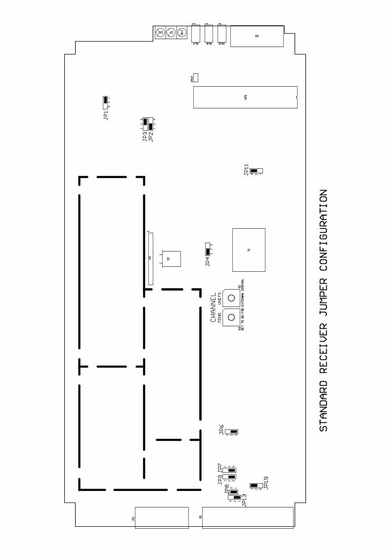
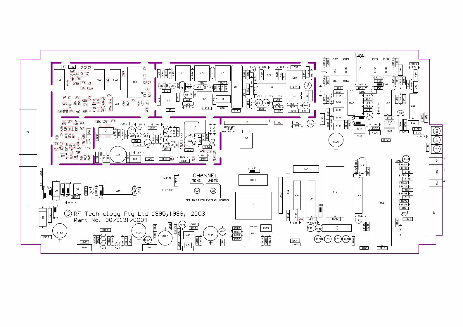
A Engineering Diagrams A.1 Block Diagram Figure 1 shows the block signal flow diagram. A.2 Circuit Diagram Figure 2 shows the detailed circuit diagram with component numbers and values. A.3 Component Overlay Diagram Figure 3 shows the PCB overlay guide with component positions.
12
34
56
ABCD
65
43
21
D C B A
Tit
le
Num
ber
Rev
isio
nSi
ze Orc
ad B
Dat
e:7-
Aug
-199
8 Sh
eet
of
File
:D
:\RFT
_Mas
terF
iles
\..\9
131-
RxU
HF-
bloc
k.sc
hD
raw
n B
y:
45 M
Hz
600
MH
z
U4
250H
z
Q10
-Q16
Fx
Flo
= Fx
- 4
5+1
3 dB
m
Flo
45 M
Hz
RSS
I
12.8
MH
z
NO
ISE
FIL
TE
R
H1 C
TC
SSD
EC
OD
ER
MO
DU
LE
TO
NE
DE
TE
CT
SUB
-TO
NE
OU
T
NO
ISE
DE
TE
CT
+ -
LIN
E O
UT
LIN
E O
UT
MO
NIT
OR
AM
P.
LIN
E A
MP.
750
uSec
MIC
RO
PRO
CE
SSO
R C
ON
TR
OL
ER
U7,
U11
-U16
A/D
RSS
I
TU
NE
V.
CA
RR
IER
SQ
. +13.
8
DATA
LOCK DETECT
TO
NE
DA
TA
SQU
EL
CH
CO
S+
CO
S-
ISO
1N
OIS
E D
ET
EC
T
TO
NE
DE
TE
CT
TO
NE
DA
TA
ASY
NC
.D
AT
A I/
O
Rx
DA
TA
Tx
DA
TA
BC
D C
HA
NN
EL
CO
DE
1 PP
M T
CX
O
PLL
IC
STE
PS
LO
OP
FIL
TE
R
HE
LIC
AL
FIL
TE
R2
RE
SON
AT
OR
RF
AM
P.4
RE
SON
AT
OR
HE
LIC
AL
FIL
TE
R
DO
UB
LE
BA
L.
MIX
ER
1st I
F A
MP.
2nd
IF A
MP.
455
KH
z A
MP.
BPF
BPF
XT
AL
FIL
TE
RX
TA
L F
ILT
ER
LIM
ITE
R/D
ISC
RIM
INA
TO
RA
UD
IO A
MP.
RSS
I BU
FFE
R
LPF
LPF
HPF
VC
O IS
OL
AT
ION
AM
PS
LO
AM
PLIF
IER
+15
dBm
L
O O
UT
PUT
2nd
MIX
ER
2nd
OSC
.
12.5
/10
KH
z
EX
T. S
Q. *
* N
OT
ON
PC
B 3
0/91
01
BN
C
FL1
Q1
FL2,
FL
3
MX
1
Q2,
Q3
XF1
C45
,C46
,L13
Q5
MA
2M
A1
MA
3M
A4
Q4
XF2
U1
Y1 45
.455
MH
zCF1
455
KH
zC
F245
5 K
Hz
U3B
U2B
U2A
U27
B4
KH
zU
2630
0 H
z
XO
1
U28
A,B
250
Hz
U27
A10
KH
zD
6,Q
17,U
17D
,U26
C
NO
ISE
DE
TE
CT
OR
U27
D
NO
ISE
AM
P.
U17
ASW
SPS
TU
5 T1
TR
AN
SFO
RM
ER
U22
A,B
U27
C
DE
-EM
PHA
SIS
U17
B
SW S
PST
S1 SW S
PST
SQ.
AL
M
Q6,
Q7
VC
O
Q27
*, U
3A
R F
Tec
hnol
ogy
17/8
Lei
ghto
n Pl
ace,
Hor
nsby
, Syd
ney,
207
7 A
ustr
alia
11/9
131/
0001
UH
F R
xR
ev 1
JBS
afte
r R
HM
21
R
EC
EIV
ER
Ju
mp
er O
pti
on
s
JP1
- 24
0 H
z N
otc
h F
ilter
P
ositi
on
N
otch
Filt
er
IN
1
-2 *
OU
T
2-3
JP
2 -
Au
dio
Res
po
nse
P
ositi
on
750
uSec
. de-
emph
asis
1
-2 *
Fla
t res
pons
e
2
-3
JP3
- A
ud
io F
ilter
in/O
ut
Pos
ition
Hi-p
ass
& N
otch
In
2
-3 *
Fla
t Res
pons
e
1
-2
JP4
- 60
0 O
hm
Lin
e d
c L
oo
p C
OS
P
ositi
on
dc L
oop
Con
figur
ed
by J
P7,
JP
8, J
P9
1-2
*
dc L
oop
Not
Use
d
2
-3
JP6
- C
OS
Po
lari
ty
Pos
ition
Act
ive
on S
igna
l
2-3
*
Act
ive
on N
o S
igna
l
1
-2
JP7,
JP
8, J
P9
- d
c L
oo
p C
OS
Co
nfi
gu
rati
on
(JP
4 1-
2)
JP7
JP
8
JP9
S
ourc
e +l
2Vdc
Loo
p
2-3
O
N
1-2
*
Fre
e S
witc
h O
utpu
t
1-
2
ON
2-
3 JP
7, J
P8,
JP
9 -
Dir
ect
Ou
tpu
t C
OS
(JP
4 2-
3)
JP7
JP
8
JP9
+12
Vdc
Dire
ct O
utpu
t
2-3
O
FF
O
FF
F
ree
Sw
itch
Out
put
1-2
O
FF
O
FF
JP11
EP
RO
M T
ype
P
ositi
on
27
C25
6
2-3
*
27
C64
1-2
T
HE
FO
LL
OW
ING
JU
MP
ER
S A
RE
VA
LID
ON
R
X P
CB
VE
RS
ION
30/
9131
/000
4 O
R L
AT
ER
JP13
– S
qu
elch
Def
eat
P
ositi
on
S
quel
ch o
pera
tion
norm
al
1-2
*
S
quel
ch D
efea
t on
activ
e lo
w in
put a
t DB
25 p
in 1
9
2-3
JP
19 –
LE
D A
larm
ou
tpu
t
Pos
ition
No
alar
m o
utpu
t
1-2
*
A
larm
LE
D s
igna
l out
put b
roug
ht to
DB
25 p
in 7
2
-3
*
= S
tand
ard
Fac
tory
Con
figur
atio
n
Related Documents