Errata Title & Document Type: Manual Part Number: Revision Date: HP References in this Manual This manual may contain references to HP or Hewlett-Packard. Please note that Hewlett- Packard's former test and measurement, semiconductor products and chemical analysis businesses are now part of Agilent Technologies. We have made no changes to this manual copy. The HP XXXX referred to in this document is now the Agilent XXXX. For example, model number HP8648A is now model number Agilent 8648A. About this Manual We’ve added this manual to the Agilent website in an effort to help you support your product. This manual provides the best information we could find. It may be incomplete or contain dated information, and the scan quality may not be ideal. If we find a better copy in the future, we will add it to the Agilent website. Support for Your Product Agilent no longer sells or supports this product. You will find any other available product information on the Agilent Test & Measurement website: www.tm.agilent.com Search for the model number of this product, and the resulting product page will guide you to any available information. Our service centers may be able to perform calibration if no repair parts are needed, but no other support from Agilent is available.

Welcome message from author
This document is posted to help you gain knowledge. Please leave a comment to let me know what you think about it! Share it to your friends and learn new things together.
Transcript
Errata
Title & Document Type:
Manual Part Number:
Revision Date:
HP References in this Manual This manual may contain references to HP or Hewlett-Packard. Please note that Hewlett-Packard's former test and measurement, semiconductor products and chemical analysis businesses are now part of Agilent Technologies. We have made no changes to this manual copy. The HP XXXX referred to in this document is now the Agilent XXXX. For example, model number HP8648A is now model number Agilent 8648A.
About this Manual We’ve added this manual to the Agilent website in an effort to help you support your product. This manual provides the best information we could find. It may be incomplete or contain dated information, and the scan quality may not be ideal. If we find a better copy in the future, we will add it to the Agilent website.
Support for Your Product Agilent no longer sells or supports this product. You will find any other available product information on the Agilent Test & Measurement website:
www.tm.agilent.com Search for the model number of this product, and the resulting product page will guide you to any available information. Our service centers may be able to perform calibration if no repair parts are needed, but no other support from Agilent is available.
Christina Samii
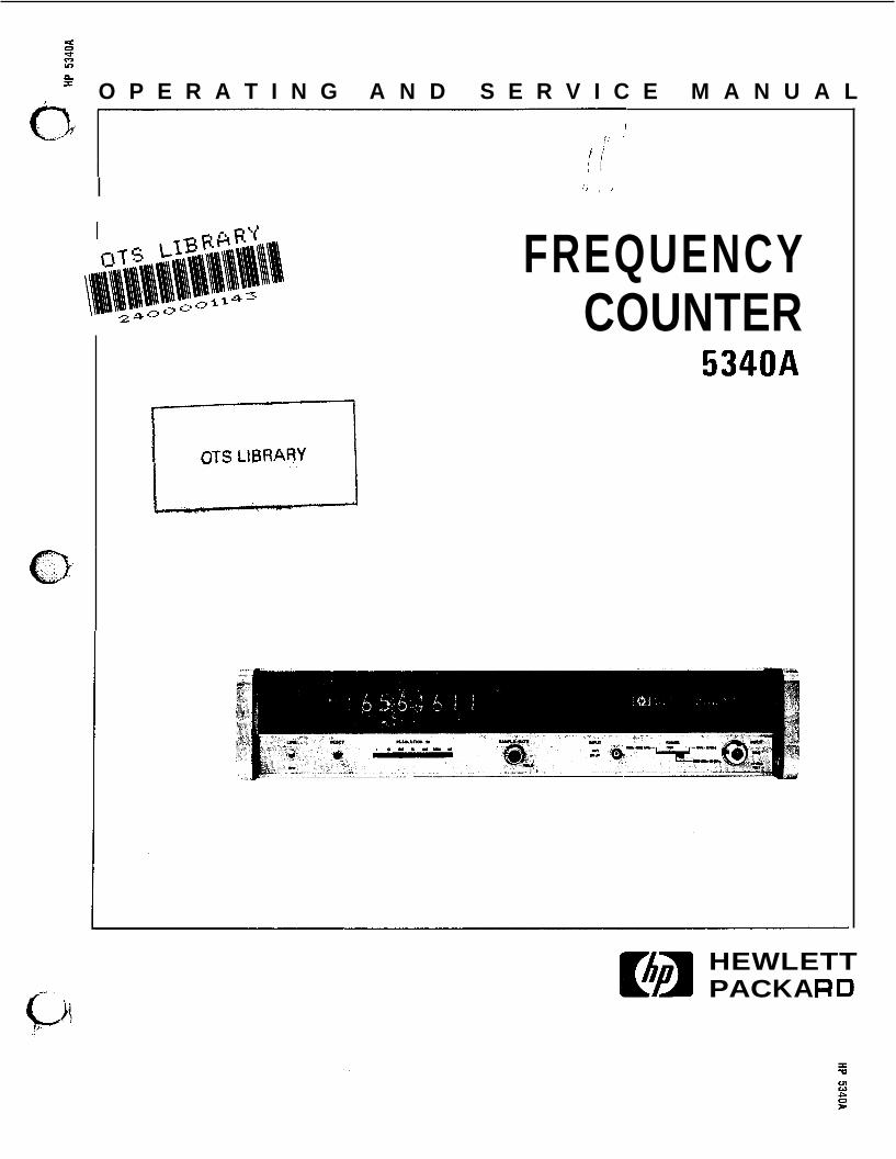
5340A Frequency Counter Operating and Service Manual
Christina Samii
05340-90021
Christina Samii
September 1975
p.
O P E R A T I N G A N D S E R V I C E M A N U A L
$ , I I
FREQUENCY COUNTER
5340A
HEWLETT P ! PAC KA R D
teritchi
Rectangle
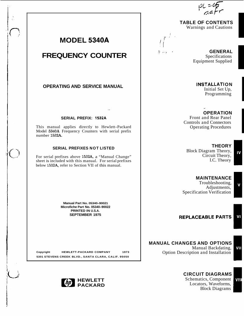
MODEL 5340A
FREQUENCY COUNTER
OPERATING AND SERVICE MANUAL
SERIAL PREFIX: 1532A
This manual applies directly to Hewlett-Packard Model 5340A Frequency Counters with serial prefix number 1532A.
SERIAL PREFIXES NOT LISTED
For serial prefixes above 1532A, a “Manual Change” sheet is included with this manual. For serial prefixes below 1532A, refer to Section VII of this manual.
Manual Part No. 05340-90021 Microfiche Part No. 05340-90022
PRINTED IN U.S.A. SEPTEMBER 1975
Copyright HEWLETT-PACKARD COMPANY 1973
5301 STEVENS CREEK BLVD., SANTA CLARA, CALIF. 95050
I I
TABLE OF CONTENTS Warnings and Cautions
I [ i 1 ’
I I
l i t ) / - GENERAL Specifications
Equipment Supplied
INSTALLATI ON Initial Set Up, Programming
I /
OPERATION Front and Rear Panel
Controls and Connectors Operating Procedures
I THEORY Block Diagram Theory,
Circuit Theory, I.C. Theory
I MAINTENANCE Troubleshooting,
Adjustments, Specification Verification
I MANUAL CHANGES AND OPTIONS Manual Backdating,
Option Description and Installation
HEWLETT PACKARD I CIRCUIT DIAGRAMS
Schematics, Component Locators, Waveforms,
Block Diagrams
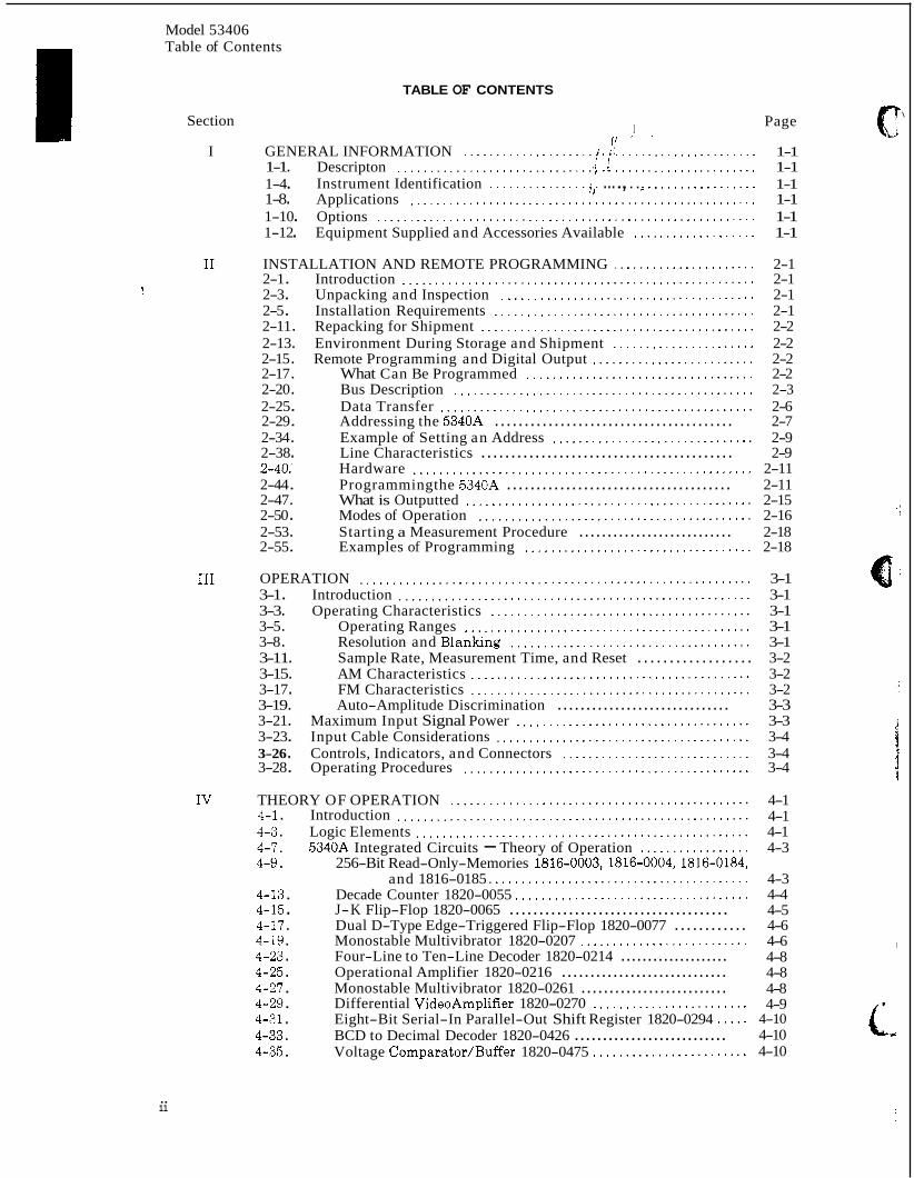
Model 53406 Table of Contents
TABLE OF CONTENTS
Page I Section I I: ' '
I GENERAL INFORMATION .................... I . 1. ...................... 1-1
I1
I
I11
. i I 1-1 . Descripton ............................... . r ...................... 1-1 1-4 . 1-1 1-8 . Applications ..................................................... 1-1 1-10 . Options .......................................................... 1-1 1-12 . Equipment Supplied and Accessories Available . . . . . . . . . . . . . . . . . . . 1-1
INSTALLATION AND REMOTE PROGRAMMING ...................... 2-1 2-1 . Introduction ...................................................... 2-1 2-3 . Unpacking and Inspection ....................................... 2-1 2-5 . Installation Requirements ........................................ 2-1 2-11 . Repacking for Shipment .......................................... 2-2
2-17 . What Can Be Programmed ................................... 2-2 2-20 . Bus Description .............................................. 2-3 2-25 . Data Transfer ................................................ 2-6 2-29 . Addressing the 5340A ........................................ 2-7 2-34 . Example of Setting an Address ............................... 2-9 2-38 . Line Characteristics .......................................... 2-9 2-40.' Hardware .................................................... 2-11 2-44 . Programmingthe 5340A ...................................... 2-11 2-47 . What is Outputted ............................................ 2-15 2-50 . Modes of Operation .......................................... 2-16 2-53 . Starting a Measurement Procedure ........................... 2-18 2-55 . Examples of Programming ................................... 2-18
OPERATION ............................................................ 3-1 3-1 . Introduction ...................................................... 3-1 3-3 . Operating Characteristics ........................................ 3-1 3-5 . Operating Ranges ............................................ 3-1 3-8 . Resolution and Blanking ..................................... 3-1 3-11 . Sample Rate, Measurement Time, and Reset . . . . . . . . . . . . . . . . . . 3-2 3-15 . AM Characteristics ........................................... 3-2 3-17 . FM Characteristics ........................................... 3-2 3-19 . Auto-Amplitude Discrimination .............................. 3-3 3-21 . Maximum Input Signal Power .................................... 3-3 3-23 . Input Cable Considerations ....................................... 3-4
3-28 . Operating Procedures ............................................ 3-4
Instrument Identification . . . . . . . . . . . . . . . ,. ... ., . . . r' . . . . . . . . . . . . . . . . .
2-13 . Environment During Storage and Shipment ...................... 2-2 2-15 . Remote Programming and Digital Output ......................... 2-2
3-26 . Controls, Indicators, and Connectors ............................. 3-4
IV THEORY OF OPERATION .............................................. 4.1 . Introduction ...................................................... 4.3 . Logic Elements ................................................... 4.7 . 5340A Integrated Circuits - Theory of Operation ................. 4.9 . 256-Bit Read-Only-Memories 1816.0003, 1816.0004, 1816.0184,
and 1816-0185 ........................................ 4.13 . Decade Counter 1820-0055 .................................... 4.15 . J-K Flip-Flop 1820-0065 ..................................... 4.17 . Dual D-Type Edge-Triggered Flip-Flop 1820-0077 ............ 4.19 . Monostable Multivibrator 1820-0207 .......................... 4.23 . Four-Line to Ten-Line Decoder 1820-0214 .................... 4.25 . Operational Amplifier 1820-0216 ............................. 4.27 . Monostable Multivibrator 1820-0261 .......................... 4.29 . Differential VideoAmplifier 1820-0270 ........................ 4.31 . Eight-Bit Serial-In Parallel-Out Shift Register 1820-0294 ..... 4.33 . BCD to Decimal Decoder 1820-0426 ........................... 4.35 . Voltage Comparator/Buffer 1820-0475 ........................
4-1 4-1 4-1 4-3
4-3 4-4 4-5 4-6 4-6 4-8 4-8 4-8 4-9
4-10 4-10 4-10
\
I
.. 11
!> 4 . 3
Model 5340A Table of Contents
TABLE OF CONTENTS (Continued)
Section 1 Page
/ i ' : ' IV THEORY OF OPERATION (Continued) 4-37 . 4-39 . 4-41 . Dual NAND Schmitt Triggers 1820-0537 ...................... 4-13 4-43 . EECL High-speed D-Binary 1820-0557 ....................... 4-13 4-45 . Dual Two-Input Logic Switch 1820-0560 ...................... 4-14 4-47 . Dual D-Type Edge-Triggered Flip-Flops 1820-0596 . . . . . . . . . . . 4-14 4-49 . Four-Input Multiplexer 1820-0610 ............................ 4-14 4.51 . Eight-Input Multiplexer 1820-0615 ........................... 4-16 4.53 . Quad 2-Input Multiplexer 1820-0616 .......................... 4-16 4.55 . Data Selectors/Multiplexers 1820-0640 ........................ 4-17 4.57 . Eight-Input Priority Encoder 1820-0657 ...................... 4-18 4.59 . Low-Power 4-Bit Shift Register 1820-0659 .................... 4-19 4.61 . Low-Power BCD Decade Counter 1820-0669 .................. 4-20 4.65 . Five-Bit Comparator 1820-0706 .............................. 4-20
4.69 . Synchronous Four-Bit Counter 1820-0716 ..................... 4-23 4.71 . Presettable Decade Counter/Latch 1820-0751 . . . . . . . . . . . . . . . . . 4-23 4.73 . EECL Differential Amplifier/Limiter 1820-0754 . . . . . . . . . . . . . . . 4-24 4.75 . Presettable Binary Counter/Latch 1820-0765 ................. 4-25 4.77 . Hex D-Type Flip-Flops 1820-0788 ............................ 4-25 4.79 . Quadruple D-Type Flip-Flops 1820-0839 ...................... 4-25 4.81 . Low Power 5-Bit Comparator 1820-0904 ...................... 4-26 4.83 . Four-Bit Binary Full Adder 1820-0910 ........................ 4-26 4.85 . EECL Bi-Quinary Counter 1820-1019 ......................... 4-26 4.87 . BCD to Decimal Decoder 1820-1047 ........................... 4-28 4.89 . Voltage Regulator 1826-0010 ................................. 4-28 4.91 . Voltage Regulator 1826-0016 .................................. 4-28 4.93 . Operational Amplifier 1826-0021 ............................. 4-28 4.95 . Voltage Comparator/Buffer 1826-0026 ........................ 4-30 4.97 . Dual Operational Amplifier 1826-0073 ........................ 4-30 4.99 . Dual Differential Amplifier 1858-0004 ........................ 4-31 4.101 . Transistor Array 1858-0018 .................................. 4-31 4.103 . Simplified Block Diagram Description ............................ 4-32 4.110 . Overall Theory of Operation ...................................... 4-32 4.112 . Input Circuits ................................................ 4-32 4.114 . Input Phase Lock Loop ....................................... 4-33 4.122 . Transfer Phase Lock Loop .................................... 4-34 4.124 . Harmonic Determination Circuitry ........................... 4-35 4.126 . Sampling Theory ................................................. 4-35 4.132 . Sampler Driver ............................................... 4-36 4.134 . When Sampling Occurs ....................................... 4-36 4.137 . 4-37 4.141 . A2 Preamplifier Assembly No . 2, 05340-60027 ..................... 4-37 4.144 . A3 High-Impedance Input Amplifier Assembly, 05340-60001 ...... 4-37 4.149 . A4 Phase DetectodQuad Detector Assembly, 05340-60002 ......... 4-38 4.154 . A5 Search Assembly, 05340-60003 ................................ 4-38 4.156 . A6 Search Programmer Assembly, 05340-60004 ................... 4-39 4.160 . A7 DC Amplifier/Compensator No . 1 Assembly, 05340-60005 ..... 4-39 4.162 . A8 Bandpass Filter/Phase Detector Assembly, 05340-60006 . . . . . . . 4-39 4.169 . A9 DC Amplifier/Compensator No . 2 Assembly, 05340-60007 ..... 4-40 4.175 . A10 VCO No . 2 Assembly,0534 0.60008 ........................... 4-42 4.182 . A l l MixerAssembly,0534 0.60009 ................................ 4-42 4.184 . A12 VCO No . 1 Assembly, 05340-60008 ........................... 4-42 4.186 . A13 Limiter/Amplifier Assembly, 05340-60010 .................... 4-43 4.188 . A14 Limiter/Amplifier/Mier Assembly, 05340-60011 . . . . . . . . . . . . . 4-43 4.191 . A15 10 MHz Doubler Assembly, 05340-60012 ...................... 4-43
Binary to Decimal Decoder 1820-0495 . . '. ...................... Dual Monostable Multivibrator lSZO-OS'i5 . .I . . ._ . . . . . . . . . . . . . . . . 4-11
4-12
4.67 . Low-Power Quad Two-Input Multiplexer 1820-0710 ........... 4-20
A1 Preamplifier Assembly No . 1,0534 0.60017 .....................
... 111
Model 5340A Table of Contents
I
TABLE OF CONTENTS (Continued)
Section I Page
4.194 . A17A1 Direct Counter Amplifier Assembly. Od3 0-60038 .......... 4-43 4.200 . A18 Standard Oscillator Assembly. 05340-60036 .................. 4-44 4.202 . A18 Option 001 Oscillator Assembly. 10544&/ .... ./ ... r . . . . . . . . . . . . . . 4-44 4-205 . A19 Interface A Assembly, 05340-60031 and A27 Resolution Switch
Assembly. 05340-60026 ............................... 4-44 4-212 . 4-45 4-229 . A20 Time Base Assembly, 05340-- 60073 .......................... 4-47
4-247 . A22 High Frequency Counter Assembly, 05340-60016 ............. 4-49 4-251 . A23 Counter Register Assembly, 05340-60030 ..................... 4-49
IV THEORY OF OPERATION (Continued) y '
A19 Interface B Assembly 05340-60032 (Part of Option 011) .......
4-236 . A21 Control Assembly, 05340-60021 .............................. 4-48
4-255 . A24 Display Register Assembly, 05340-60019 ..................... 4-50 4-258 . A25 Display Assembly, 05340-60020 .............................. 4-50 4-265 . A26 Blanking Assembly, 05340-60037 ............................ 4-51 4-267 . Power Supplies ................................................... 4-51
(Part of Option 001) .................................. 4-51 4-269 .
4-273 . A32 +5 Volt Regulator Assembly, 05340-60023 ................ 4-52 4-278 . A29 +15 Volt Regulator Assembly, 05340-60025 ............... 4-53 4-280 . A28 -15 Volt and +175 Regulator Assembly, 05340-60022 ...... 4-53 4-283 . A31 -5 Volt Regulator Assembly, 05340-60024 ................. 4-54 4-285 . A34 Bus Communicator Assembly, 05340-60067
(Part of Option 011) .................................. 4-54 4-287 . Talk Mode ................................................... 4-54 4-290 . Listen Mode .................................................. 4-54
A33 Optional Oscillator Power Supply Assembly, 05340-60039,
V MAINTENANCE AND SERVICE ........................................ 5-1 5.1 . Introduction ...................................................... 5-1 5.3 . Assembly Designations ........................................... 5-1 5.5 . Test Equipment .................................................. 5-1 5.7 . Pozidriv Screwdrivers ............................................ 5.1 .
5.9 . Adjustments and In-Cabinet Performance Check ................. 5-1 5.11 . Blower Fan Configuration ........................................ 5-1 5.13 . K05-5340A Description ........................................... 5-1 5.16 . Program Control Flow Diagrams ................................. 5-14 5.24 . Overall Troubleshooting .......................................... 5-17 5.26 . A20 N Checker Troubleshooting .............................. 5-18 5.35 . A21 Troubleshooting ......................................... 5-19 5.39 . Power Supply Troubleshooting ............................... 5-20
VI REPLACEABLE PARTS ................................................. 6-1 6.1 . Introduction ...................................................... 6-1 6.4 . Ordering Information ............................................ 6-3 6.7 . HP Part Number Organization ................................... 6-3 6.9 . Component Parts and Materials .............................. 6-4 6.12 . General Usage Parts ......................................... 6-4 6.14 . Specific Instrument Parts .................................... 6-4
VII MANUAL CHANGES AND OPTIONS ................................... 7-1 7.1 . Introduction ...................................................... 7-1
7.5 . New Instruments ............................................. 7-1 7-7 . Older Instruments ............................................. 7-1 7-9 . Options .......................................................... 7-16 7-11 . Option 001, High-Stability Oscillator ......................... 7-16 7-13 . Option 002, Rear Panel Connectors ........................... 7-16 7-15 . Option 011, Remote Programming and Digital Output . . . . . . . . . 7-16 7-19 . Field Installation of Options ...................................... 7-16 7-20 . Installation of Option 001, High-Stability Oscillator .......... 7-16
7.3 . Manual Changes ................................................. 7-1
iv
Model 5340A Table of Contents
List of Tables
TABLE OF CONTENTS (Continued)
VII MANUAL CHANGES AND OPTIONS (Continued) I / 7.23 . Installation of Option 002. Rear Panel Connectors ............ 7-18 7.26 . Installation of Option 011. Digital Inpuh'Output: .............. 7-19
VIII SCHEMATIC! DIAGRAMS ............................................... 8-1
Table 1.1 . 1.2 . 1.3 . 2.1 . 2.2 . 2.3 . 2.4 . 2.5 . 2.6 .
4.1 . 4.2 .
5.1 . 5.2 . 5.3 .
6.1 . 6.2 . 6.3 . 6.4 . 6.5 . 6.6 . 7.1 . 7.2 .
8.1 . . .
8.1 . Schematic Diagrams ............................................. 8-1
Reference Designators ................................ 8-1 8-5 . Reference Designations ....................................... 8-1 8.8 . Identification Markings on Printed-Circuit Boards ............ 8-1 8.12 . Assembly Locations and Component Locators .................... 8-1 8-14 . Mnemonics and Abbreviations ................................... 8-2
8.3 . Schematic Diagram Notes, Assembly Numbers. and
LIST OF TABLES
Page Equipment Supplied ...................................................... 1-2 Accessories Available .................................................... 1-2 Specifications ............................................................ 1-3
Relation of ATN and the Handshake Lines (RFD. DAC. DAV) ............ 2-5 Talk and Listen Addresses ............................................... 2-8 Program Code Set ........................................................ 2-10 5340A Program Code Set ................................................. 2-13 5340A Output Code Set ................................................... 5340A Programming Example ............................................ 2-19
2-15
Example ROM Programming for the Equation Y=2X+1 .................... 4-4 Time Base Signal Selection ............................................... 4-47
Assembly Identification .................................................. 5-2 Recommended Test Equipment ........................................... 5-3 In-Cabinet Performance Check ........................................... 5-13
Replaceable Parts. 5340A Standard Instruments .......................... 6-5 5340A Mechanical Parts .................................................. 6-33 Replaceable Parts. Option 001 ............................................ 6-34 Replaceable Parts. Option 002 ............................................ 6-35 Replaceable Parts. Option 011 ............................................ 6-36 Manufacturers Code List ................................................. 6-38
Manual Backdating ...................................................... 7-1 A20 Time Base Board Assembly (Series 1236A). Replaceable Parts . . . . . . . . . . 7-6
5340A Mnemonics and Abbreviations ..................................... 8-2
V
Model 5340A List of Figures
Figure I 1.1 . 2.1 . 2.2 . 2.3 . 2.4 . 2.5 . 2.6 .
I 3.1 . ‘ 3.2 .
3.3 . 3.4 . 3.5 . 3.6 .
4.1 . 4.2 . 4.3 .
4.4 . 4.5 . 4.6 . 4.7 . 4.8 . 4.9 .
4.10 . 4.11 . 4.12 . 4.13 . 4.14 . 4.15 . 4.16 . 4.17 . 4.18 . 4.19 . 4.20 . 4.21 . 4.22 . 4.23 . 4.24 . 4.25 . 4.26 . 4.27 . 4.28 . 4.29 . 4.30 . 4-3 1 . 4.32 . 4.33 . 4.34 . 4.35 . 4.36 .
i 4.37 . 4.38 . 4.39 . 4.40 .
vi
LIST OF FIGURES
Page
1-0 b
Model 5340A Frequency Counter. Rack Mount Kit. an fower Cord ....... 9 J Handshake Timing ................................ ..... #. . . . . . . . . . . . . . . . . . 2-6 5340A Rear Panel ........................................ .I .............. 2-11 5340A Digital Input/Output .............................................. 2-12 Pin Connections of the 10631A. B. C Cables .............................. 2-12 5340A Remote Operation ................................................. 2-17 Example Program Card .................................................. 2-20
FM Characteristics ....................................................... 3-2 DBM to Volts Conversion ................................................ 3-3 Front Panel Controls and Indicators ...................................... 3-5 Rear Panel Controls and Connectors ...................................... 3-7 5340A Operating Procedures .............................................. 3-8 Self Check and Operational Check Procedures ............................ 3-9
Logic Comparison Diagrams ............................................. 4-1 Gate Symbols ............................................................ 4-2 Logic Diagram for 1816.0003. 1816.0004. 1816.0184. and
1816-1085 ROM’S ..................................... 4-3 Decade Counter 1820-0055 ................................................ 4-5 J-K Flip-Flop 1820-0065 ................................................. 4-5 Dual D-Type Edge-Triggered Flip-Flop 1820-0077 ........................ 4-6 Four-Bit Binary Counter 1820-0099 ....................................... 4-7 Monostable Multivibrator 1820-0207 ...................................... 4-7 Four-Line to Ten-Line Decoder 1820-0214 ................................ 4-8 Operational Amplifier 1820-0216 ......................................... 4-8 Monostable Multivibrator 1820-0261 ...................................... 4-9 Differential Video Amplifier 1820-0270 ................................... 4-9 Eight-Bit Serial-In Parallel-Out Shift Register 1820-0294 ................. 4-10 BCD to Decimal Decoder 1820-0426 ....................................... 4-11 Voltage Comparator/Buffer 1820-0475 .................................... 4-11 Binary to Decimal Decoder 1820-0495 ..................................... 4-12 Dual Monostable Multivibrator 1820-0515 ................................ 4-12 Dual NAND Schmitt Triggers 1820-0537 .................................. 413 EECL High-speed D-Binary 1820-0557 ................................... 4-13 Dual Two-Input Logic Switch 1820-0560 .................................. 4-14 Dual D-Type Edge Trigger FlipFlop 1820-0596 ........................... 4-15 Four-Input Multiplexer 1820-0610 ........................................ 4-15 Eight-Input Multiplexer 1820-0615 ....................................... 4-16 Quad 2-Input Multiplexer 1820-0616 ....................................... Data Selectors/Multiplexers 1820-0640 .................................... 4-17 Eight-Input Priority Encoder 1820-0657 .................................. 4-18 Low-Power 4-Bit Shift Register 1820-0659 ................................ 4-19 Low-Power DCB Decade Counter 1820-0669 .............................. 4-21 Five-Bit Comparator 1820-0706 .......................................... 4-22 Low-Power Quad Two-Input Multiplexer 1820-0710 ....................... 4-22 Synchronous Four-Bit Counter 1820-0716 ................................. 4-23 Presettable Decade Counter/Latch 1820-0751 ............................. 4-24 EECL Differential Amplifier/Limiter 1820-0754 ........................... 4-24 Hex D-Type Flip-Flop 1820-0788 ......................................... 4-25 Quadruple D-Type Flip-Flop 1820-0839 ................................... 4-26 Four-Bit Binary Full Adder 1820-0910 .................................... 4-27 EECL Bi-Quinary Counter 1820-1019 ..................................... 4-27 Voltage Regulator 1826-0010 ............................................. 4-28 Voltage Regulator 1826-0016 ............................................. 4-29 Operational Amplifier 1826-0021 ......................................... 4-29
4-17
Model 5340A
Figure
4.41 . 4.42 . 4.43 . 4.44 . 4.45 . 4.46 . 4.47 . 4.48 . 4.49 . 4.50 . 4.51 . 4.52 .
5.1 . 5.2 . 5.3 . 5.4 . 5.5 .
6.1 .
7.1 . 7.2 . 7.3 . 7.4 . 7.5 . 7.6 . 7.7 . 7.8 . 7.9 . 7.10 .
8.1 . 8.2 . 8.3 .
8.4 . 8.5 .
8.6 . 8.7 . 8.8 . 8.9 . 8.10 . 8.11 . 8.12 . 8.13 . 8.14 . 8.15 . 8.16 . 8.17 . 8.18 . 8.19 . 8.20 . 8.21 . 8.22 . 8.23 .
I List of Figures
LIST OF FIGURES (Continued)
Page F
Voltage Comparator/Buffer 1826-0026 I ’ 4-30 ..................................... I~
Operational Amplifier 1826-0073 ................. ..! . / .................... 4-30 Dual Differential Amplifier 1858-0004 .................................... 4-31 Transistor Array 1858-0018. ...................... !i . ...I . . . . : ............... 4-31 Simplified Block Diagram ................................................ 4-33 Sampling Diode Switch ................................................... 4-35 Balanced Sampler ......................................................... 4-35
I .
Sampler Slot ................................................................ 4-36 Sampling Timing ........................................................ 4-36 Frequency Response of A9 Input . Amplifier ............................... 4-40 Transfer Loop Timing Diagram .......................................... 4-41 Equivalent Regulator Circuit ............................................. 4-52
K05-5340A Feed-Forward Simulator. Schematic Diagram ................. Adjustment Procedures ................................................... 5-4 Simplified Flow Diagram of 5340A Program Control ...................... Troubleshooting Flow Diagram with HP Logic Clip’ ....................... Troubleshooting Charts 1 through 3 ...................................... .‘5-21
5340A Mechanical Parts .................................................. 6-32
5-3
5-15 5-16
A2 Component Locator Series 1236A ...................................... 7-6 A17 Direct Count Amplifier Assembly (Series 1220A) ...................... 7-7 A17A1 Direct Count Amplifier Assembly (Series 1220A) . . . . . . . . . . . . . . . . . . . 7-8 A20 Time Base Assembly ................................................. 7-9 A20 Component Locator (Series 1236A) 7-10 A10 VCO No . 2 Assembly (Series 1220A) Schematic Diagram ............. 7-11 A12 VCO No . 1 Assembly (Series 1220A) Schematic Diagram ............. 7-12 A10. A12 VCO No . 1 and No . 2 Component Locator ....................... 7-13 A33 Power Supply (Series 1236A). Schematic Diagram .................... 7-14 A33 Power Supply (Series 1236A). Component Locator .................... 7-15
Schematic Diagram Notes ................................................ 8-3 5340A Top Internal View (with Options 001. 002. and 011 Installed) .......
Options 001.002. and 011 Installed) .............................. 8-5 5340A Front Panel Reference Designations ............................... 8-7
011 Installed) .................................................... 8-7
...................................
8-4 5340A Bottom Internal View and Cable Numbers and Connections (with
5340A Rear Panel Reference Designations (with Options 002 and
5340ABlock Diagram .................................................... 8-9 8-11 8-13 8-15 8-17
A1 Preamplifier Assembly No . 1 .......................................... A2 Preamplifier Assembly No . 2 .......................................... A3 HI-Z Input Amplifier Assembly ....................................... A4 Phase/Quad Detector Assembly ....................................... A5 Search Assembly ..................................................... 8-19 A6 Search Programmer Assembly ........................................ 8-21 A7 DC Amplifier/Compensator No . 1 Assembly ........................... A8 Bandpass Filters/@ Detector Assembly ................................ A9 DC Amplifier/Compensator No . 2 Assembly ........................... A10 VCO No . 2 Assembly ................................................ 8-29 A l l Mixer Assembly ..................................................... 8-31 A12 VCO No . 1 Assembly ................................................ 8-33 A13 Limiter/Amplifier Assembly ......................................... 8-35 A14 Limiter/Amplifier/Mixer Assembly .................................. 8-37 A15 10 MHz Doubler Assembly ........................................... A16 Casting Motherboard ................................................ 8-41 A17 Direct Count Amplifier Assembly .................................... 8-43
8-23 8-25 8-27
8-39
vii
Model 5340A List of Figures
Figure I 8-24.
8-25.
8-26. 8-27. 8-28. 8-29. 8-30.
1 8-31. 8-32. 8-33.
8-34.
8-35. 8-36.
... vlll
LIST OF FIGURES (Continued)
Page I
A18 Standard 10 MHz Oscillator Assembly A18 10 M $Oscillator Assembly (Option 001) . . . . . . . . . . . . . . . . . . .
A19 Interface A Assembly (Standard Instrument), 11 A27 Resolution Switch Assembly . . . . . . . . . . , . :: ?. . .'. . . . . . . . . . . . . . . 8-47
A19 Interface B Assembly (Part of Option 011) . . . . . . . . . . . . . . . . . . . . . . . . . . , . 8-49 A20 Time Base Assembly . , . . . . . . . . . . . . . . . . . . . . . . . . . . . . . . . . . . . . . . . . . . . . . . . 8-53 A21 Control Assembly . . . . . . . . . . . . . . . . . . . . . . . . . . . . . . . . . . . . . . . . . . . . . . . . . . . . 8-55 A22 High Frequency Counter Assembly . . . . . . . . . . . . . . . . . . . . . . . . . . . . . . . . . . 8-59 A23 Count Register Assembly . . . . . . . . . . . . . . . . . . . . . . . . . . . . . . . . . . . . . . . . . . . . 8-61 A24 Display Register Assembly . . . . . . . . . . . . . . . . . . . . . . . . . . . . . . . . . . . . . . . . . . . 8-63 A25 Display Assembly, A26 Blanking Assembly . . . . . . . . . . . . . . . . . . . . . . . . . . 8-65 A28 -15V and +175V Regulators Assembly, A29 +15V Regulator Assembly,
A30 Power Supply Motherboard . . . . . . . . . . . . . . . . . . . . . . . . . . . . . . . . . . 8-69 A30 Power Supply Motherboard, A31 -5V Regulator Assembly,
A32 +5V Regulator Assembly . . . . . . . . . . . . . . . . . . . . . . . . . . . . . . . . . . . . . 8-75 A33 Optional Oscillator Power Supply (Part of Option 001) . . . . . . . . . . . . . . . . 8-77 A34 Bus Communicator Assembly . . . . . . . . . . . . . . . . . . . . . . . . . . . . . . . . . . . . . . . . 8y79
.. ... . . ........ .. . 8-45 $I 'I. .I .
Model 5340A
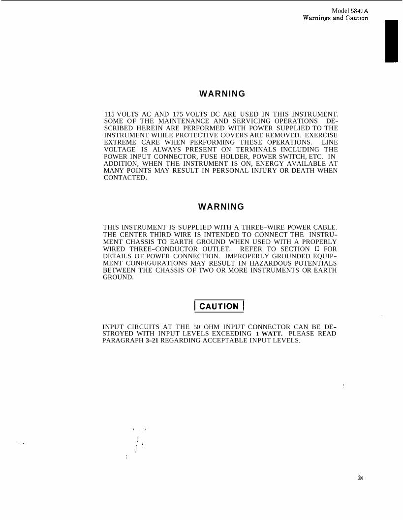
WARNING
115 VOLTS AC AND 175 VOLTS DC ARE USED IN THIS INSTRUMENT.
SCRIBED HEREIN ARE PERFORMED WITH POWER SUPPLIED TO THE INSTRUMENT WHILE PROTECTIVE COVERS ARE REMOVED. EXERCISE EXTREME CARE WHEN PERFORMING THESE OPERATIONS. LINE VOLTAGE IS ALWAYS PRESENT ON TERMINALS INCLUDING THE POWER INPUT CONNECTOR, FUSE HOLDER, POWER SWITCH, ETC. IN ADDITION, WHEN THE INSTRUMENT IS ON, ENERGY AVAILABLE AT MANY POINTS MAY RESULT IN PERSONAL INJURY OR DEATH WHEN CONTACTED .
SOME OF THE MAINTENANCE AND SERVICING OPERATIONS DE-
WARNING
THIS INSTRUMENT IS SUPPLIED WITH A THREE-WIRE POWER CABLE. THE CENTER THIRD WIRE IS INTENDED TO CONNECT THE INSTRU- MENT CHASSIS TO EARTH GROUND WHEN USED WITH A PROPERLY WIRED THREE-CONDUCTOR OUTLET. REFER TO SECTION I1 FOR DETAILS OF POWER CONNECTION. IMPROPERLY GROUNDED EQUIP- MENT CONFIGURATIONS MAY RESULT IN HAZARDOUS POTENTIALS BETWEEN THE CHASSIS OF TWO OR MORE INSTRUMENTS OR EARTH GROUND.
INPUT CIRCUITS AT THE 50 OHM INPUT CONNECTOR CAN BE DE-
PARAGRAPH 3-21 REGARDING ACCEPTABLE INPUT LEVELS. STROYED WITH INPUT LEVELS EXCEEDING 1 WATT. PLEASE READ
, , ', !
:i , ' i
I
ix
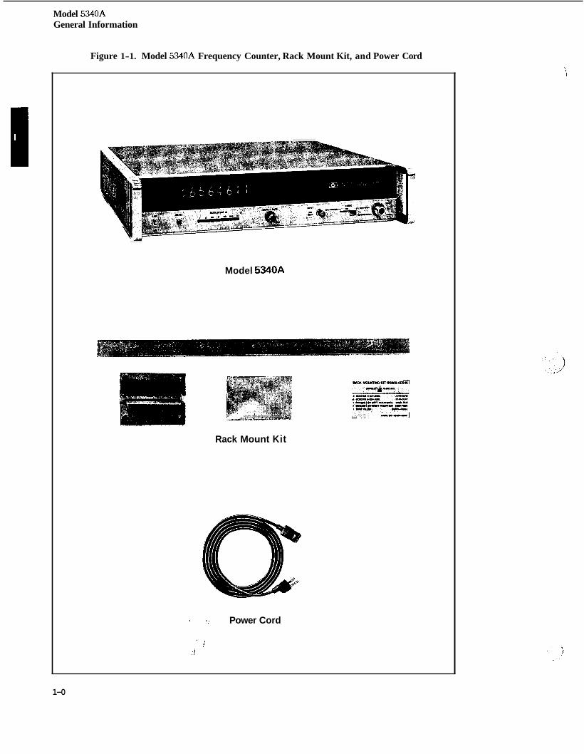
Model 5340A General Information
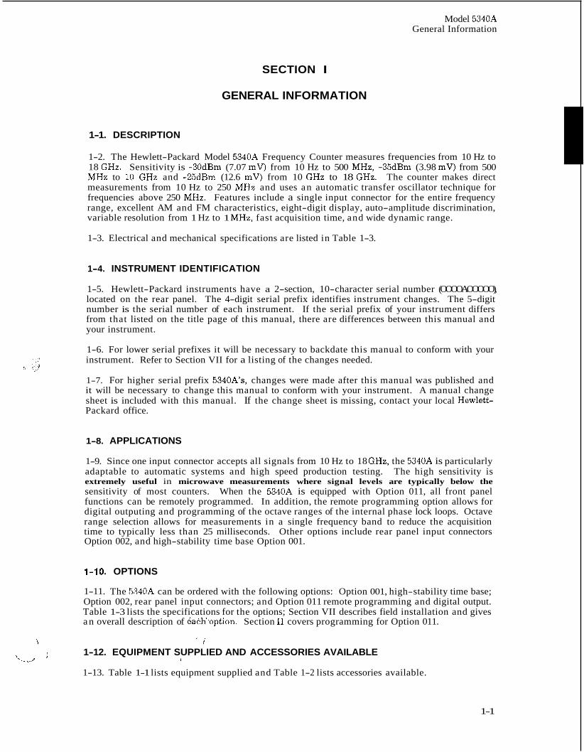
Figure 1-1. Model 5340A Frequency Counter, Rack Mount Kit, and Power Cord
Model 5340A
I ‘1 Power Cord
’ ! . i
Rack Mount Kit
1-0
SECTION I
GENERAL INFORMATION
1-1. DESCRIPTION
1-2. The Hewlett-Packard Model 5340A Frequency Counter measures frequencies from 10 Hz to 18 GHz. Sensitivity is -30dBm (7.07 mV) from 10 Hz to 500 MHz, -35dBm (3.98 mV) from 500 MHz to 10 GHz and -25dBm (12.6 mV) from 10 GHz to 18 GHz. The counter makes direct measurements from 10 Hz to 250 MHz and uses an automatic transfer oscillator technique for frequencies above 250 MHz. Features include a single input connector for the entire frequency range, excellent AM and FM characteristics, eight-digit display, auto-amplitude discrimination, variable resolution from 1 Hz to 1 MHz, fast acquisition time, and wide dynamic range.
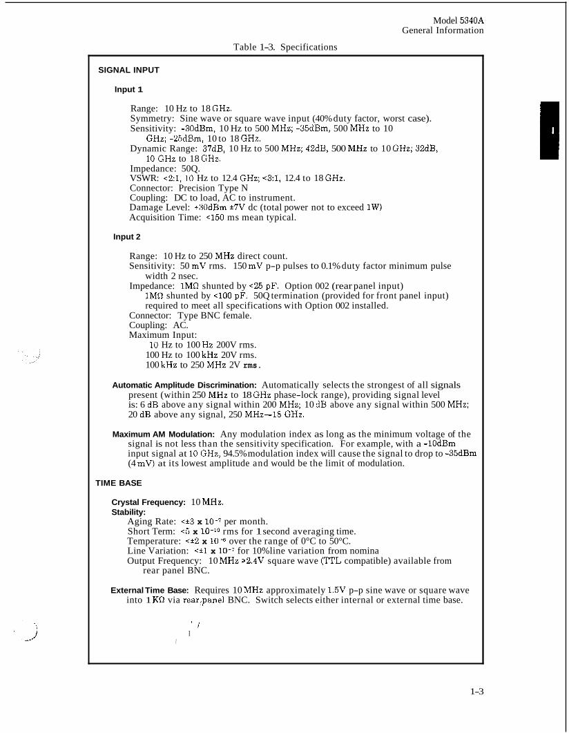
1-3. Electrical and mechanical specifications are listed in Table 1-3.
1-4. INSTRUMENT IDENTIFICATION
1-5. Hewlett-Packard instruments have a 2-section, 10-character serial number (OOOOAOOOOO), located on the rear panel. The 4-digit serial prefix identifies instrument changes. The 5-digit number is the serial number of each instrument. If the serial prefix of your instrument differs from that listed on the title page of this manual, there are differences between this manual and your instrument.
1-6. For lower serial prefixes it will be necessary to backdate this manual to conform with your instrument. Refer to Section VII for a listing of the changes needed.
’/ J 1-7. For higher serial prefix 5340A’s, changes were made after this manual was published and it will be necessary to change this manual to conform with your instrument. A manual change sheet is included with this manual. If the change sheet is missing, contact your local Hewlett- Packard office.
1-8. APPLICATIONS
1-9. Since one input connector accepts all signals from 10 Hz to 18 GHz, the 5340A is particularly adaptable to automatic systems and high speed production testing. The high sensitivity is extremely useful in microwave measurements where signal levels are typically below the sensitivity of most counters. When the 5340A is equipped with Option 011, all front panel functions can be remotely programmed. In addition, the remote programming option allows for digital outputing and programming of the octave ranges of the internal phase lock loops. Octave range selection allows for measurements in a single frequency band to reduce the acquisition time to typically less than 25 milliseconds. Other options include rear panel input connectors Option 002, and high-stability time base Option 001.
Model 5340A General Information
I
1-10. OPTIONS
1-11. The 5340A can be ordered with the following options: Option 001, high-stability time base; Option 002, rear panel input connectors; and Option 011 remote programming and digital output. Table 1-3 lists the specifications for the options; Section VII describes field installation and gives a n overall description of each’poption. Section I1 covers programming for Option 011.
1 ‘ I 1-12. EQUIPMENT SUPPLIED AND ACCESSORIES AVAILABLE
‘..-I I
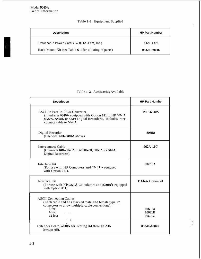
1-13. Table 1-1 lists equipment supplied and Table 1-2 lists accessories available.
1-1
Model 5340A Genral Information
Description
Detachable Power Cord 7-% ft. (231 cm) long
Rack Mount Kit (see Table 6-1 for a listing of parts)
Table 1-1. Equipment Supplied
HP Part Number
8120-1378
05326-60046
Description I Table 1-2. Accessories Available
HP Part Number
ASCII to Parallel BCD Converter (Interfaces 5340A equipped with Option 011 to HP 5050A, 5050B, 5055A, or 562A Digital Recorders). Includes inter- connect cable to 5340A.
Digital Recorder (Use with K01-5340A above).
Interconnect Cable (Connects K01-5340A to 5050A/B, 5055A, or 562A Digital Recorders).
Interface Kit (For use with HP Computers and 5340A's equipped with Option 011).
Interface Kit (For use with HP 982OA Calculators and 5340A's equipped with Option 011).
ASCII Connecting Cables (Each cable end has stacked male and female type 57 connectors to allow multiple cable connections).
3 feet 6 feet I /
12 feet
t I , !
:I Extender Board, 6340A for Testing A4 through A15
(except A5).
K01-5340A
505512
562A-16C
59310A
11144A Option 20
10631A 10631B 10631C
05340-60047
1-2
Model 5340A General Information
Table 1-3. Specifications
SIGNAL INPUT
Input 1
Range: 10 Hz to 18 GHz. Symmetry: Sine wave or square wave input (40% duty factor, worst case). Sensitivity: -30dBm, 10 Hz to 500 MHz; -35dBm, 500 MHz to 10
Dynamic Range: 37dB, 10 Hz to 500 MHz; 42dB, 500 MHz to 10 GHz; 32dB,
Impedance: 50Q. VSWR: <2:1, 10 Hz to 12.4 GHz; <3:1, 12.4 to 18 GHz. Connector: Precision Type N Coupling: DC to load, AC to instrument. Damage Level: +30dBm *7V dc (total power not to exceed 1W) Acquisition Time: <150 ms mean typical.
GHz; -25dBm, 10 to 18 GHz.
10 GHz to 18 GHz.
Input 2
Range: 10 Hz to 250 MHz direct count. Sensitivity: 50 mV rms. 150 mV p-p pulses to 0.1% duty factor minimum pulse
width 2 nsec. Impedance: 1MQ shunted by <25 pF. Option 002 (rear panel input)
1MQ shunted by <lo0 pF. 50Q termination (provided for front panel input) required to meet all specifications with Option 002 installed.
Connector: Type BNC female. Coupling: AC. Maximum Input:
10 Hz to 100 Hz 200V rms. 100 Hz to 100 kHz 20V rms. 100 kHz to 250 MHz 2V rms.
Automatic Amplitude Discrimination: Automatically selects the strongest of all signals present (within 250 MHz to 18 GHz phase-lock range), providing signal level is: 6 dB above any signal within 200 MHz; 10 dB above any signal within 500 MHz; 20 dB above any signal, 250 MHz-18 GHz.
Maximum AM Modulation: Any modulation index as long as the minimum voltage of the signal is not less than the sensitivity specification. For example, with a -10dBm input signal at 10 GHz, 94.5% modulation index will cause the signal to drop to -35dBm (4 mV) at its lowest amplitude and would be the limit of modulation.
TIME BASE
Crystal Frequency: 10 MHz. Stability:
Aging Rate: <*3 x Short Term: <5 x Temperature: <*2 x 10+ over the range of 0°C to 50°C. Line Variation: <*l x for 10% line variation from nomina Output Frequency: 10 MHz 32.4V square wave (TTL compatible) available from
per month. rms for 1 second averaging time.
rear panel BNC.
External Time Base: Requires 10 MHz approximately 1.5V p-p sine wave or square wave into 1 KO via rear,panel BNC. Switch selects either internal or external time base.
I i I
I
1-3
Model 5340A General Information
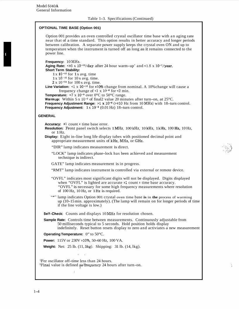
Table 1-3. Specifications (Continued)
OPTIONAL TIME BASE (Option 001)
Option 001 provides a n oven controlled crystal oscillator time base with a n aging rate near that of a time standard. This option results in better accuracy and longer periods between calibration. A separate power supply keeps the crystal oven ON and up to temperature when the instrument is turned off as long as it remains connected to the power line.
Frequency: 10 MHz. Aging Rate: <*5 x 10-’O/day after 24 hour warm-up’ and <1.5 x 10⁻⁷/year. Short Term Stability:
1 x 10+0 for 1 s avg. time 1 x 2 x
for 10 s avg. time. for 100 s avg. time.
Line Variation: <1 x
Temperature: <7 x over 0°C to 50°C range. Warmup: Within 5 x 10⁻⁹ of final2 value 20 minutes after turn-on, at 25°C. Frequency Adjustment Range: >1 x Frequency Adjustment: 1 x (0.01 Hz) 18-turn control.
for *lo% change from nominal. A 10% change will cause a frequency change of <1 x 10⁴ for <2 min.
(>*lo Hz from 10 MHz) with 18-turn control.
GENERAL
Accuracy: * l count f time base error. Resolution: Front panel switch selects 1 MHz, 100 kHz, 10 kHz, 1 kHz, 100 Hz, 10 Hz,
Display: Eight in-line long life display tubes with positioned decimal point and or 1 Hz.
appropriate measurement units of kHz, MHz, or GHz.
“DIR” lamp indicates measurement is direct.
“LOCK” lamp indicates phase-lock has been achieved and measurement
GATE” lamp indicates measurement is in progress.
“RMT” lamp indicates instrument is controlled via external or remote device.
technique is indirect.
“OVFL” indicates most significant digits will not be displayed. Digits displayed when “OVFL” is lighted are accurate *1 count * time base accuracy. “OVFL” is necessary for some high frequency measurements where resolution of 100 Hz, 10 Hz, or 1 Hz is required.
“*” lamp indicates Option 001 crystal oven time base is in the process of warming up (10-15 min. approximately). (The lamp will remain on for longer periods of time if the line voltage is low.)
Self-check: Counts and displays 10 MHz for resolution chosen.
Sample Rate: Controls time between measurements. Continuously adjustable from 50 milliseconds typical to 5 seconds. Hold position holds display indefinitely. Reset button resets display to zero and activiates a new measurement
Operating Temperature: 0” to 50°C.
Power: 115V or 230V *lo%, 50-60 Hz, 100 VA. Weight: Net: 25 lb. (11, 3kg). Shipping: 31 lb. (14, lkg).
, I
’For oscillator off-time less than 24 hours. 2Final value is defined asifrequency 24 hours after turn-on.
i I
1-4
Model 5340A General Information
Table 1-3. Specifications (Continued)
GENERAL (CONTINUED)
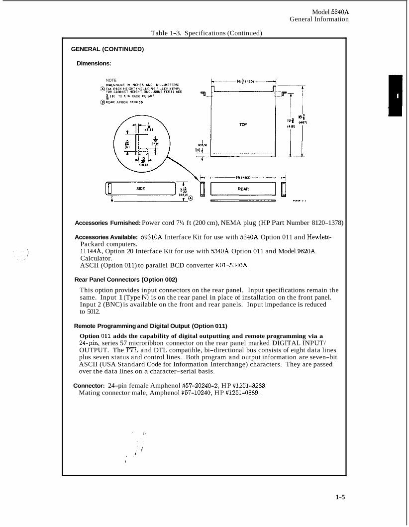
Dimensions:
NOTE
$ IB) TO E l A RACK HEIGHT
@ R E A R APRON RECESS
Accessories Furnished: Power cord 7% ft (200 cm), NEMA plug (HP Part Number 8120-1378)
Accessories Available: 59310A Interface Kit for use with 5340A Option 011 and Hewlett- Packard computers. 11144A, Option 20 Interface Kit for use with 5340A Option 011 and Model 9820A Calculator. ASCII (Option 011) to parallel BCD converter K01-5340A.
Rear Panel Connectors (Option 002)
This option provides input connectors on the rear panel. Input specifications remain the same. Input 1 (Type N) is on the rear panel in place of installation on the front panel. Input 2 (BNC) is available on the front and rear panels. Input impedance is reduced to 5012.
Remote Programming and Digital Output (Option 011)
Option 011 adds the capability of digital outputting and remote programming via a 24-pin, series 57 microribbon connector on the rear panel marked DIGITAL INPUT/ OUTPUT. The TTL and DTL compatible, bi-directional bus consists of eight data lines plus seven status and control lines. Both program and output information are seven-bit ASCII (USA Standard Code for Information Interchange) characters. They are passed over the data lines on a character-serial basis.
Connector: 24-pin female Amphenol #57-20240-2, HP #1251-3283. Mating connector male, Amphenol #57-10240, HP #1251-0389.
1-5
2-1. INTRODUCTION
2-2. This section tells how to set up the 5340A Frequency Counter. Instructions for unpacking, inspecting, installing, and remote programming are included.
2-3. UNPACKING AND INSPECTION
2-4. If the shipping carton is damaged, inspect the counter for visible damage (scratches, dents, etc.). If the counter is damaged, notify the carrier and the nearest Hewlett-Packard Sales and Service Office immediately (offices are listed at the back of this manual). Keep the shipping carton and packing material for the carrier’s inspection. The Hewlett-Packard Sales and Service Office will arrange for repair or replacement of your instrument without waiting for the claim against the. camer to be settled.
2-5. INSTALLATION REQUIREMENTS
BEFORE CONNECTING THE INSTRUMENT TO AC POWER LINES, BE SURE THAT THE LINE SELECTOR IS PROPERLY POSITIONED.
.*< 3 .-
2-6. LINE VOLTAGE REQUIREMENTS. The 5340A is equipped with a line voltage switch to select 115-volt or 230-volt ac operation. Before applying power, the rear panel screwdriver- operated switch must be set to the correct position (“115” or “230” visible) and the correct fuse (as labeled on the rear panel) must be installed. See Figure 3-4 for rear panel features.
2-7. between 48 Hz and 66 Hz.
LINE FREQUENCY REQUIREMENTS. The counter will operate at line frequencies
2-8. THREE CONDUCTOR POWER CABLE. To protect the operator, the counter uses a grounded three-conductor detachable power cable. The male connector end is a NEMA type connector, and the female connector end is a C.E.E. type connector that mates with the 5340A rear panel power connector. Connect the power cable to a power source receptacle with a NEMA grounded third conductor. If the line power receptacle is a standard two-pin type instead of the NEMA three-pin receptacle, use a two-to-three pin adaptor (HP Part No. 8120-1348) and connect the green pigtail on the adaptor to ground.
2-9. TEMPERATURE LIMITS. Maximum and minimum allowable operating temperatures ake listed in Table 1-3. If these limits are exceeded at the installation site, auxiliary cooling or heating should be used to keep the environment within limits.
Model 5340A Installation and Remote Programming
SECTION II
INSTALLATION AND REMOTE PROGRAMMING
I
2-10. RACK INSTALLATION. The counter is ready for bench operation as shipped from the factory. Additional parts necessary for rack mounting are packaged with the instrument. To convert the instrument to ‘rack installation, refer to Figure 6-1 for parts identification and pro- ceed as follows:
,’ i a. Remove tilt stand MP14 by removing the two outside front feet MPl l from the bottom
cover MP9. 1 The feet are removed by pressing the foot-release button and sliding the foot toward the center of the instrument.
b. Remove the remaining three feet from the bottom cover. 2-1
Model 5340A Installation and Remote Programming
c. Remove the two adhesive-backed trim strips MP1 from side frames MP3 and MP12.
d. Using the three screws provided, attach the filler strip from the rack mount kit along the front of bottom cover MP9.
e. Attach the flanges from the rack mount kit to the front end of side frames MP3 and MP12. Orient the larger corner notch toward the bottom of the instrument.
2-11. REPACKING FOR SHIPMENT
2-12. If it becomes necessary to reship a counter, good commercial packing should be used. Contract packaging companies in many cities can provide dependable custom packaging on short notice. Instruments should be packed securely in a strong corrugated container (350 lb/sq. in bursting test) with suitable filler pads between the instrument and container. Before returning instruments to Hewlett-Packard, contact the nearest Hewlett-Packard Sales and Service Office for instructions.
2-13. ENVIRONMENT DURING STORAGE AND SHIPMENT
2-14. Conditions during storage and shipment should normally be limited as follows:
a. Maximum altitude: 25,000 feet. b. Minimum temperature: -40°F (-40OC). c. Maximum temperature: +167’F (+75OC).
2-15. REMOTE PROGRAMMING AND DIGITAL OUTPUT
2-16. Option 011 adds remote programming and digital output capability to the 5340A Frequency Counter. These are accomplished with a bi-directional bus, via a 24-pin connector on the rear panel marked DIGITAL INPUT/OUTPUT. Associated with this connector are six slide switches used to address the instrument. A 5340A can be addressed to either send output data (TALK) or to accept program information (LISTEN). For the purposes of the Option 011 description, several terms are defined as follows:
a. A TALKER is the sender of information on the bus.
b. A LISTENER is the receiver or acceptor of information on the bus.
c. A CONTROLLER is a n instrument that has the responsibility of managing the instru- ments connected to the bus. It is capable of addressing other instruments on the bus as TALKERS or as LISTENERS. It is a TALKER and may be a LISTENER.
“High” or ‘‘0” level of a line or switch is the relatively more positive signal level (22.4V).
“Low” or “1” level of a line or switch is the relatively less positive signal level (~0.4V).
d.
e.
2-17. What Can Be Programmed
2-18. Also, the 5340A’s octave range and its output mode can be selected. In addition, a controller can command the 5340A to make a measurement by sending either a SAMPLE TRIGGER or RESET instruction. The controller can elect 40 give control to the front panel controls (LOCAL) or have the 5340A operate according to ’the information stored in its remote program storage cells (REMOTE). These are listed in Table 2-,kl along with their associated codes.
2-19. When addressed 40 Ohput, the 5340A sends a string of 16 ASCII characters (USA Standard Code for Information fnterchange). It includes the measurement technique (direct or by using phase locked loops), overflow, eight data digits (blank display digits are outputed as 0’s) E
All front panel switch functions, except power, are programmable.
i
2-2
Model 5340A Installation and Remote Programming
followed by the appropriate multiplier to make the reading Hz, and a word terminator. Table 2-5 lists the order outputed and a description of the 16 output characters.
2-20. Bus Description
2-21. The 15-line bus consists of 8 data lines plus 7 control and status lines. Addresses, program and output information are communicated on the data lines. These are based on a character-serial, seven-bit ASCII code set.
2-22. Three control lines are used to execute the transfer of each byte of information on the data lines. They employ an interlocked “handshake” technique to pass information. This allows for asynchronous data transfer without timing restrictions being placed on either the 5340A or its controller. One line is driven by the 5340A to inform the controller of its status. The controller uses the three remaining lines to manage the 5340As on the bus.
2-23. Several 5340A’s can be connected to a common bus. The exact number depends on the drive capability of the controller (see LINE CHARACTERISTICS). A specific 5340A is made to send output data (TALK) or accept program data (LISTEN) by addressing it to do so.
2-24. All bus lines have been given names and mnemonic acronyms that convey the message being carried on that line. Each line is described below, followed by Table 2-1 which lists the relationship of the Attention line and the three handshake lines. Figure 2-1 shows the signal levels and timing relationship of the handshake and data lines. ALL INSTRUMENTS CONNECT- ED TO THE BUS, INCLUDING THE CONTROLLER, MUST OBEY THESE DESCRIPTIONS.
a. SERVICE REQUEST (SRQ)
By setting SRQ low, a 5340A indicates to the controller that it has completed a measure- ment and is ready to output. It drives SRQ only if programmed to “WAIT” in the output phase of its operating cycle until addressed to output. When programmed in the other output mode “output ONLY IF addressed”, the 5340A sets SRQ high at all times. When SRQ is high, service is not being requested.
If two or more 5340A’s are connected to the bus and one of them sets SRQ low, the controller must go through a process of elimination to determine which one requested service. It does this by addressing each one to TALK in a n orderly manner. Only the 5340A with output information will respond.
b. REMOTE ENABLE (REN)
REN can be used by a controller to select remote or local (front panel) control of the operating of a 5340A. I t works in conjunction with the information stored in the local- remote program storage cell (see Table 2-4). When REN is low and the 5340A has been sent an ASCII “0”, it will operate according to the information previously stored in its remote-local program storage cells. It operates according to its front panel con- trols for all other combinations of these, i.e., REN is low and the remote-local storage cell contains an ASCII “N” or when REN is high regardless of what is stored in the1 remote-local cell. ASCII “N” is stored in the local-remote program storage cell when either the power is turned on or the RESET pushbutton is depressed.
c. INTERFACE CLEAR (IFC) , I
A controller uses IFC to clear the bus. When it sets IFC low for >lo0 psec, all 5340A’s immediately stop driving the data lines (DIO1 through DI07) and handshake lines (RFD, DAC, and OAV). IFC will not clear a 5340A’s service request (SRQ). A con- troller may dride IFC low at any time. When IFC is high, it has no effect on the bus operation. The 5340A monitors IFC at all times.
2-3
Model 5340A Installation and Remote Programming
d. ATTENTION (ATN)
ATN is used by a controller to address a 5340A. The 5340A monitors ATN at all times. When ATN is low, all 5340A’s connected to the bus interpret the information on the data lines’ as an address. They will handshake on the appropriate lines and will not drive the data lines. The 5340A requires the controller to hold ATN low for 1 psec before it sets the handshake line DATA VALID low.
When ATN is high, a 5340A that has been addressed to TALK will drive the data lines. Those that have been addressed to LISTEN will interpret the information on the data lines as program data. Those that have not been addressed will not drive the data lines.
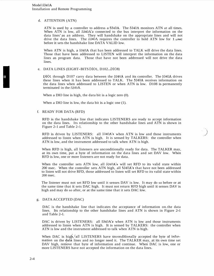
e. DATA LINES (EIGHT-BITS DIO1, D102 ... DI08)
DIOl through D107 carry data between the 5340A and its controller. The 5340A drives these lines when it has been addressed to TALK. The 5340A receives information on the data lines when addressed to LISTEN or when ATN is low. D108 is permanently terminated in the 5340A.
When a DIO line is high, the data bit is a logic zero (0).
When a DIO line is low, the data bit is a logic one (1).
f. READY FOR DATA (RFD)
RFD is the handshake line that indicates LISTENERS are ready to accept information on the data lines. Its relationship to the other handshake lines and ATN is shown in Figure 2-1 and Table 2-1.
RFD is driven by LISTENERS: all 5340A’s when ATN is low and those instruments addressed to listen when ATN is high. It is sensed by TALKERS: the controller when ATN is low, and the instrument addressed to talk when ATN is high.
When RFD is high, all listeners are unconditionally ready for data. The TALKER may, at its own time, put a byte of information on the data lines and set DAV low. When RFD is low, one or more listeners are not ready for data.
When the controller sets ATN low, all 5340A’s will set RFD to its valid state within 200 nsec. When the controller sets ATN high, all 5340As that have not been addressed to listen will not drive RFD, those addressed to listen will set RFD to its valid state within 200 nsec.
The listener must not set RFD low until it senses DAV is low. It may do so before or at the same time that it sets DAC high. It must not return RFD high until it senses DAV is high and may do so after, or at the same time that it sets DAC low.
g. DATA ACCEPTED (DAC)
DAC is the handshake line that indicates the acceptance of information on. the data lines. Its relationship to the other handshake lines and ATN is shown in Figure 2-1 and Table 2-1.
DAC is driven by LISTENERS: all 5340As when ATN is low and those instruments addressed to listen when ATN is high. It is sensed by TALKERS: the controller when ATN is low and the instrument addressed to talk when ATN is high.
When DAC is hig ,/all LISTENERS have anconditionally accepted the byte of infor-
DAV high, remove that byte of information and continue. When DAC is low, one or more LISTENERS have not accepted the information on the data lines.
mation on the dat P lines and no longer need it. The TALKER may, at its own time set
2-4
Model 5340A Installation and Remote Programming
READY FOR DATA (RFD)
LOW HIGH
One or more All 5340A’s 5340A’s not are ready ready for for data data
When the controller sets ATN low, all 5340As will set DAC to its valid state within 200 nsec. When the controller sets ATN high, the 5340A’s that have not been addressed to listen will not drive DAC, those addressed to listen will set DAC to its valid state within 200 nsec.
DATA ACCEPTED (DAC)
LOW HIGH
One or more All 5340A‘S 5340As has have not accepted accepted the data the data
The listener must not set DAC low until it senses DAV is high. It may do so before or at the same time that it sets RFD high. It must not return DAC high until it senses DAV is low and may do so after or at the same time that it sets RFD low.
h. DATA VALID (DAV)
DAV is the handshake line that indicates the validity of information on the data lines. Its relationship to the other handshake lines and ATN is shown in Figure 2-1 and Table 2-1.
It is driven by TALKERS: the controller when ATN is low and by the instrument addressed to talk when ATN is high. It is sensed by LISTENERS: all, 5340A’s if ATN is low and by the instruments addressed to listen when ATN is high.
When DAV is low, the states of data lines DIOl through D107 are unconditionally valid and may be accepted by all listeners at their own time. To allow for cable rise time, ringing, etc., the 5340A, when addressed to TALK, does not set DAV low until 2 ysec after it has placed valid data at its output connector. It assumes that the controller has taken similar precautions. DAV can only be driven low if RFD and IFC are high. When DAV is high, the information on the data lines is not valid. DAV cannot be set high unless DAC is high and RFD is low.
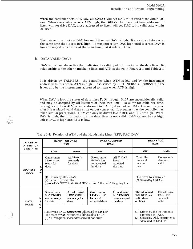
Table 2-1. Relation of ATN and the Handshake Lines (RFD, DAC, DAV)
STATE OF ATTENTION LINE (ATN)
L ADDRESS 0
MODE W
n DATA I MODE G
H
(1) Driven by all 5340As (2) Sensed by controller (3) 5340A’s drives to its valid state within 200 ns of ATN going low
have accepted for data accepted data the data
(1) Driven by ALLNstruments addressed to LISTEN (2) Sensed by thp instrument addressed to TALK (3) All instrqments not addressed w ill not drive
LOW HIGH
Controller Controller’s has valid data not data on valid lines
(1) Driven by controller (2) Sensed by 5340A’s
The addressed The addressed TALKER has TALKERS valid data data not on lines valid
(1) Driven by the instruments
(2) Sensed by ALL instruments addressed to TALK
addressed to LISTEN
2-5
Model 5340A Installation and Remote Programming
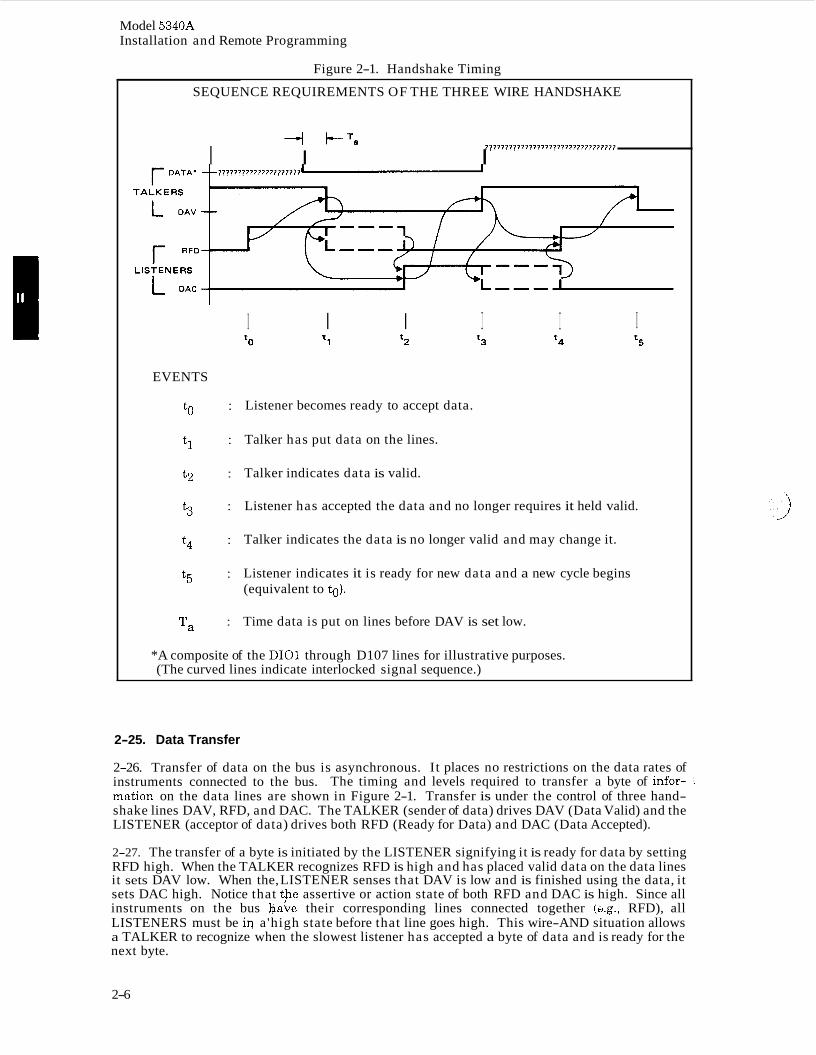
Figure 2-1. Handshake Timing ~~
SEQUENCE REQUIREMENTS OF THE THREE WIRE HANDSHAKE
. . . . . . . . . . . . . . . . . . . . . . . . . . . . . . . . . -4 +-a
I I I
I t5
I t4
I t3
I t2
I I
EVENTS
t0
tl
t2
t3
t4
t5
'a
: Listener becomes ready to accept data.
: Talker has put data on the lines.
Talker indicates data is valid.
Listener has accepted the data and no longer requires it held valid.
Talker indicates the data is no longer valid and may change it.
:
:
:
: Listener indicates it is ready for new data and a new cycle begins (equivalent to to).
: Time data is put on lines before DAV is set low.
*A composite of the DIOl through D107 lines for illustrative purposes. (The curved lines indicate interlocked signal sequence.)
2-25. Data Transfer
2-26. Transfer of data on the bus is asynchronous. It places no restrictions on the data rates of instruments connected to the bus. mation on the data lines are shown in Figure 2-1. Transfer is under the control of three hand- shake lines DAV, RFD, and DAC. The TALKER (sender of data) drives DAV (Data Valid) and the LISTENER (acceptor of data) drives both RFD (Ready for Data) and DAC (Data Accepted).
The timing and levels required to transfer a byte of infor- :,
2-27. The transfer of a byte is initiated by the LISTENER signifying it is ready for data by setting RFD high. When the TALKER recognizes RFD is high and has placed valid data on the data lines it sets DAV low. When the, LISTENER senses that DAV is low and is finished using the data, it sets DAC high. Notice that tpe assertive or action state of both RFD and DAC is high. Since all instruments on the bus have their corresponding lines connected together (e.g., RFD), all LISTENERS must be iq a'high state before that line goes high. This wire-AND situation allows a TALKER to recognize when the slowest listener has accepted a byte of data and is ready for the next byte.
2-6
Model 5340A Installation and Remote Programming
2-28. Let’s look at the timing of the transition to the non-assertive state for these lines. DAV may be driven high by the TALKERS after it recognizes that DAC is high. RFD may be set low as soon as the LISTENER recognizes that DAV has been set low. The 5340A requires RFD to be set low no later than 50 nsec after the LISTENER sets DAC high. When the 5340A is a listener it drives RFD low at the same time it sets DAC high. The timing of DAC is similar to RFD, i.e., it may go low as soon as DAV is high and it must be low no later than 50 nsec after RFD is driven high. The 50 nsec permits a controller, when working with only one 5340A on the bus, to generate either DAC or RFD and invert it to get the other.
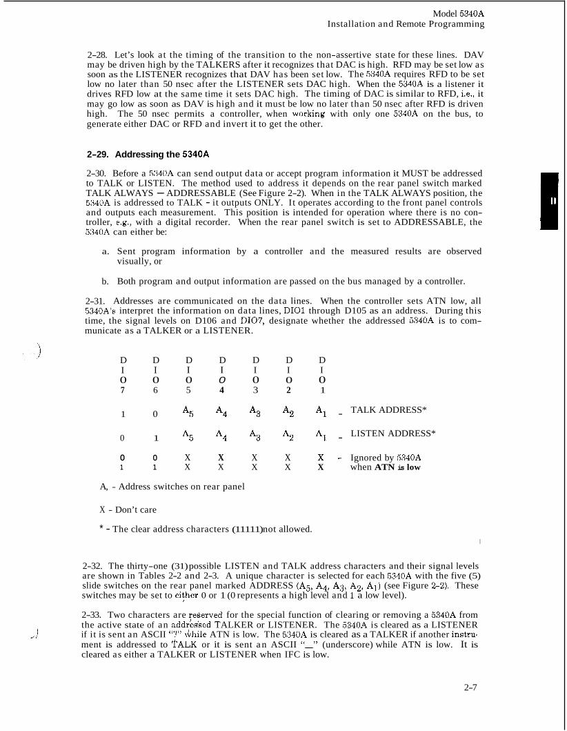
2-29. Addressing the 534044
2-30. Before a 5340A can send output data or accept program information it MUST be addressed to TALK or LISTEN. The method used to address it depends on the rear panel switch marked TALK ALWAYS - ADDRESSABLE (See Figure 2-2). When in the TALK ALWAYS position, the 5340A is addressed to TALK - it outputs ONLY. It operates according to the front panel controls and outputs each measurement. This position is intended for operation where there is no con- troller, e.g., with a digital recorder. When the rear panel switch is set to ADDRESSABLE, the 5340A can either be:
a. Sent program information by a controller and the measured results are observed visually, or
Both program and output information are passed on the bus managed by a controller. b.
2-31. Addresses are communicated on the data lines. When the controller sets ATN low, all 5340A’s interpret the information on data lines, DIOl through D105 as an address. During this time, the signal levels on D106 and DI07, designate whether the addressed 5340A is to com- municate as a TALKER or a LISTENER.
D D D D D D D I I I I I I I 0 0 0 0 0 0 0 7 6 5 4 3 2 1
1 0 A5 A4 A3 A2 A1 -
0 1 A5 A4 A3 A2 A1 -
0 0 X X X X x - 1 1 X X X X X
TALK ADDRESS*
LISTEN ADDRESS*
Ignored by 5340A when ATN is low
A, - Address switches on rear panel
X - Don’t care
* - The clear address characters (11111) not allowed. I
2-32. The thirty-one (31) possible LISTEN and TALK address characters and their signal levels are shown in Tables 2-2 and 2-3. A unique character is selected for each 5340A with the five (5) slide switches on the rear panel marked ADDRESS (A5, A4, A3, A2, A1) (see Figure 2-2). These switches may be set to ei4her 0 or 1 (0 represents a high level and 1 a low level).
2-33. Two characters are yeserved for the special function of clearing or removing a 5340A from the active state of an addredsed TALKER or LISTENER. The 534014 is cleared as a LISTENER if it is sent an ASCII “?” dhile ATN is low. The 5340A is cleared as a TALKER if another instru- ment is addressed to qALK or it is sent a n ASCII ‘‘-” (underscore) while ATN is low. It is cleared as either a TALKER or LISTENER when IFC is low.
,’ i
2-7
Model 5340A Installation and Remote Programming
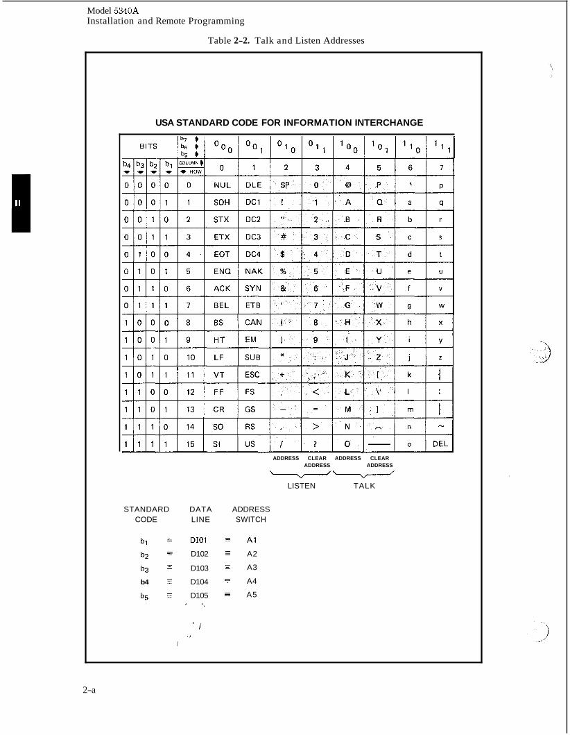
Table 2-2. Talk and Listen Addresses
USA STANDARD CODE FOR INFORMATION INTERCHANGE
ADDRESS CLEAR ADDRESS CLEAR ADDRESS ADDRESS --
LISTEN TALK
STANDARD DATA ADDRESS CODE LINE SWITCH
b l DIOI E A1
b2 E D102 A2
b3 D103 A3
b4 5 D104 E A4
b5 Z D105 E A5 ' I ,
' 1 .i
I
2-a
Model 5340A Installation and Remote Programming
5340A ADDRESS SWITCH RESULTANT LISTEN SETTINGS ADDRESS
2-34. Example of Setting an Address
RESULTANT TALK ADDRESS
2-35. Except for ? and - (underscore), any talk-listen address combination in the shaded areas of Table 2-2 can be used. Selecting a particular listen address will result in a corresponding talk address or vice versa. For example, if the ASCII # symbol is chosen for the listen address, then ASCII “C” would be the corresponding talk address. This can be seen in Tables 2-2 and 2-3 and as follows:
D107 D106 D105 D104 D103 D102 DIOl - BUSDATALINES b7 b6 b5 b4 b3 b2 b l - ASCIIBITS 0 1 0 0 0 1 1 - LISTEN ADDRESS = #
1 0 0 0 0 1 1 - TALK ADDRESS = C A5=O A4=O A3=O A2=1 A1=1 - ADDRESS SWITCHES
A5 A4 A 3 A 2 A 1
0 0 0 1 1
0 0 1 0 0
0 1 0 1 0
1 1 1 0 0
2-36. Note that for a given setting of the address switches, the listen address is determined by driving D107 to 0 and D106 to 1. The talk address is implemented by driving D107 to 1 and D106 to 0. Table 2-3 lists the available address codes.
# C
$ D
* J
< \
2-37. Other examples of 5340A talk listen addresses are as follows:
I I
S I 1 0 0 1 3
2-38. Line Characteristics
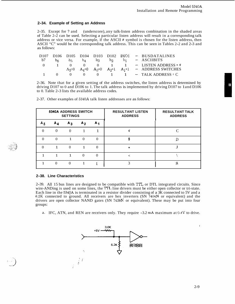
2-39. All 15 bus lines are designed to be compatible with n‘L or DTL integrated circuits. Since wire-ANDing is used on some lines, the TTL line drivers must be either open collector or tri-state. Each line in the 534QA is terminated in a resistor divider consisting of a 3K connected to 5V and a 6.2K connected to ground. All receivers are hex inverters (SN 7404N or equivalent) and the drivers are open collector NAND gates (SN 7438N or equivalent). These may be put into four groups:
a. IFC, ATN, and REN are receivers only. They require -3.2 mA maximum at 0.4V to drive.
>*p SN 7404N
I
2-9
Model 5340A Installation and Remote Programming
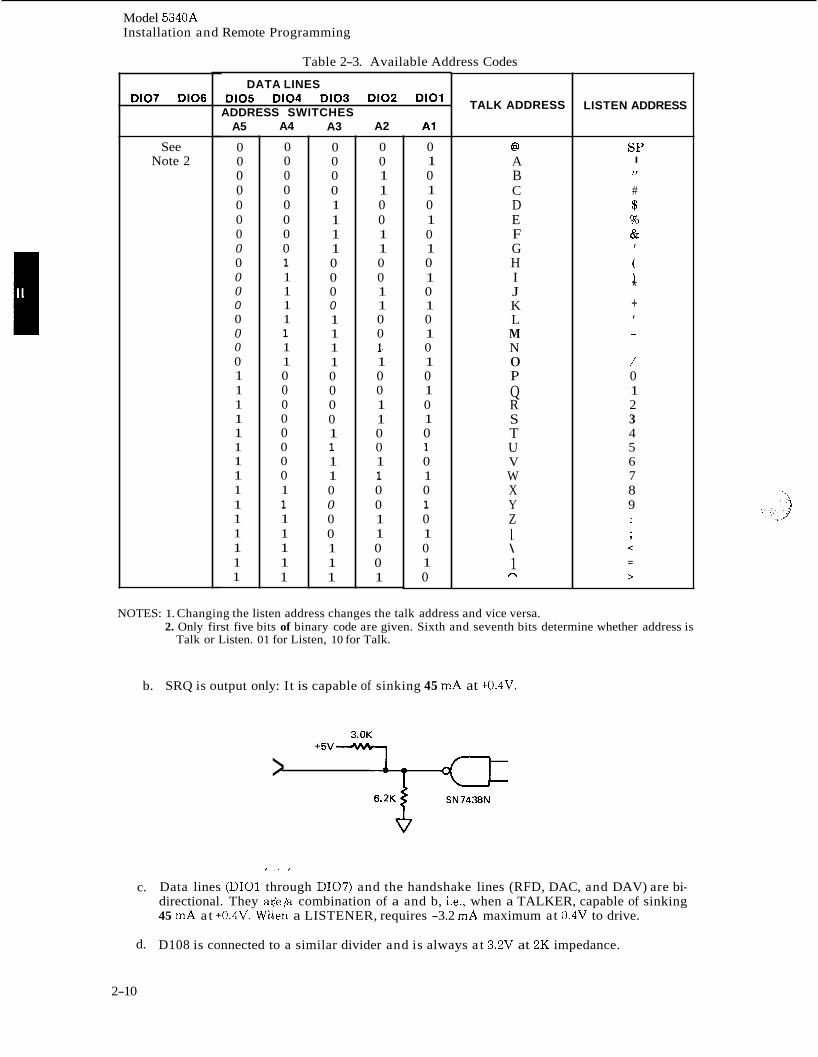
D107 D106
See Note 2
Table 2-3. Available Address Codes
DATA LINES D105 D104 D103 D102 D l O l
ADDRESS SWITCHES A5
0 0 0 0 0 0 0 0 0 0 0 0 0 0 0 0 1 1 1 1 1 1 1 1 1 1 1 1 1 1 1
A4
0 0 0 0 0 0 0 0 1 1 1 1 1 1 1 1 0 0 0 0 0 0 0 0 1 1 1 1 1 1 1
A3
0 0 0 0 1 1 1 1 0 0 0 0 1 1 1 1 0 0 0 0 1 1 1 1 0 0 0 0 1 1 1
A2
0 0 1 1 0 0 1 1 0 0 1 1 0 0 1. 1 0 0 1 1 0 0 1 1 0 0 1 1 0 0 1
A1
0 1 0 1 0 1 0 1 0 1 0 1 0 1 0 1 0 1 0 1 0 1 0 1 0 1 0 1 0 1 0
TALK ADDRESS
@ A B C D E F G H I J K L M N 0 P Q R S T U V W X Y Z [ \ 1 n
LISTEN ADDRESS
SP I
I I
# $ % &
( )
I
* + I
-
/ 0 1 2 3 4 5 6 7 8 9
NOTES: 1. Changing the listen address changes the talk address and vice versa. 2. Only first five bits of binary code are given. Sixth and seventh bits determine whether address is
Talk or Listen. 01 for Listen, 10 for Talk.
b. SRQ is output only: It is capable of sinking 45 mA at +0.4V.
3.OK +5v
>
, ,
c. Data lines (DIO1 through DI07) and the handshake lines (RFD, DAC, and DAV) are bi- directional. They aje /a combination of a and b, i.e., when a TALKER, capable of sinking 45 mA a t +0.4V. WMen a LISTENER, requires -3.2 mA maximum at 0.4V to drive.
d. D108 is connected to a similar divider and is always a t 3.2V at 2K impedance.
2-10
Model 5340A Installation and Remote Programming
2-40. Hardware
2-41. The 5340A's digital INPUT/OUTPUT connector is on the rear panel (Figure 2-2). Pin con- nections to this Type 57 Microribbon connector are shown in Figure 2-3.
2-42. Cables of three different lengths are available for connecting a 5340A to a controller or to another 5340A:
a. b. c.
3 feet long HP Part No. 10631A. 6 feet long HP Part No. 10631B.
12 feet long HP Part No. 10631C.
2-43. These have one overall shield to reduce susceptibility to external noise. The cables use a mixture of individual wires and twisted pairs to reduce crosstalk. Both ends are identical. They are terminated in two 24-pin piggy back connectors; one male and one female. This termination permits several cables to be connected to the same 5340A. Pin connections of these connectors are shown in Figure 2-4. There is a restriction of no more than 12-feet between the first two in- struments in the system and 6-feet between the remaining instruments. The 5340A can drive a maximum of 50-feet of this cable.
2-44. Programming the 5340A
2-45. The 5340A has a group of storage cells that are used to store program information. They are used ONLY when a controller has the 5340A operating under remote control. The ASCII char- acters that can be stored in each cell and their relationship to the 5340As operation are shown in Table 2-4. (Refer to Table 2-2 for signal levels.)
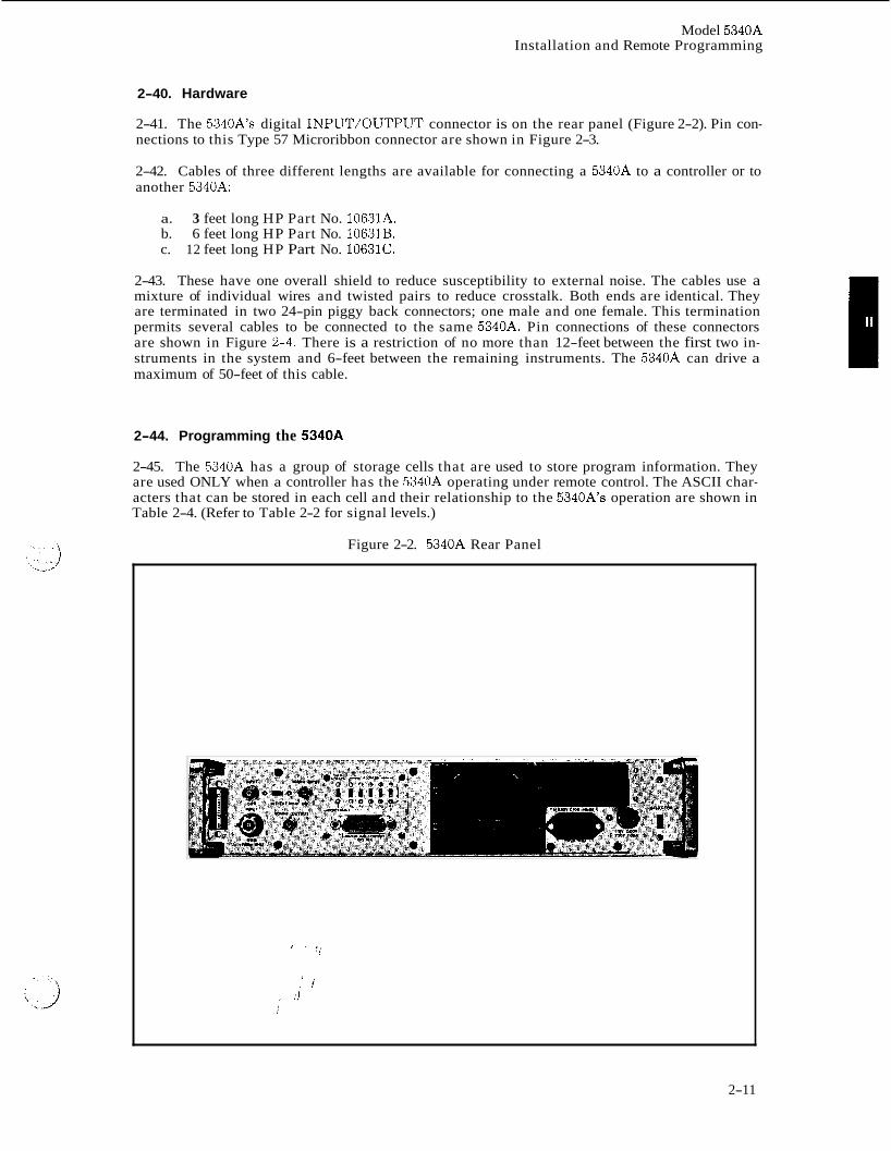
Figure 2-2. 5340A Rear Panel
2-11
Model 5340A Installation and Remote Programming
Figure 2-3. 5340A Digital Input/Output
DID1
D102
D103
DI04
RESERVED
DAV
RFD
D I05
D I06
D107
DIOB
REN
P/O TWISTED PAIR WITH 6
P/O TWISTED PAIR WITH 7
SHOULD BEGRDUNDED NEAR OF OTHER WIRE OF
P/O TWISTED PAIR WITH 9
P/O TWISTED PAIR WITH 10
P/O TWISTED PAIR WITH 8 r IFC
SRD
PI0 TWISTED PAIR WITH 11
SIGNAL GROUND ADDRESSABLE 0
TALK ALWAYS 9 w TYPE 57 MICRORIBBON CONNECTOR
~~ ~~~~~
Figure 2-4. Pin Connections of the 10631A, B, C Cables
DIOl
D102
DI03
D I M
RESERVED
DAV
RFD
D AC
IFC
SRO
ATN
GROUND W Y AT SHIELD SYSTEM CONTROLLER
' ',
I /
D 105
DI06
DI07
DIOB
REN
i P/O TWISTED PAIR WITH 6
P/O TWISTED PAIR WITH 7
P/O TWISTED PAIR WITH 8
P/O TWISTED PAIR WITH 9
P/O TWISTED PAIR WITH 10
P/O TWISTED PAIR WITH 11
SIGNAL GROUND
SHOULD BE GROUNDED NEAR TERMINATION OF OTHER WIRE OF TWISTED PAIR
w TYPE 57 MICRORIBBON CONNECTOR
..I NOTE 1: P,ins 18 through 23 should be grounded near the termination of the other wire of its twisted pair. Pin 12 is grounded ONLY at the controller.
2-12
Model 5340A Installation and Remote Programming
Table 2-4. 5340A Program Code Set
Binary ASCII‘
0 1 2 3 4 5 6
Octal
060 061 062 063 064 065 066
,123 125 124 120
1 10 100 1K 10K lOOK 1M
100 10’ 102 103 104 105 106
0 1 1 0 0 0 0 0 1 1 0 0 0 1 0 1 1 0 0 1 0 0 1 1 0 0 1 1 0 1 1 0 1 0 0 0 1 1 0 1 0 1 0 1 1 0 1 1 0
Ranges 10 Hz - 250 MHz (hi Z) Check 250 MHz - 18 GHz (50R) 10 HZ - 18 GHz (50R)
S U T P
1 0 1 0 0 1 1 1 0 1 0 1 0 1 1 0 1 0 1 0 0 1 0 1 0 0 0 0
~~~ ~ ~
1 0 0 0 0 0 0 1 0 0 0 0 0 1 1 0 0 0 0 1 0 1 0 0 0 0 1 1 1 0 0 0 1 0 0 1 0 0 0 1 0 1 1 0 0 0 1 1 0 1 0 0 0 1 1 1
Octave Ranges (use with T&P only) Auto 38 GHz 4 GHz - 8 GHz 2 GHz - 4 GHz 1 GHz - 2 GHz 500 MHz - 1 GHz 250 MHz - 500 MHz 10 HZ - 250 MHz
100 101 102 103 104 105 106 107
c A B C D E F G
Sample Rate Internal Sample Rate Hold
J K
1 0 0 1 0 1 0 1 0 0 1 0 1 1
112 113
I 1 0 0 1 0 0 1 111 SAMPLE TRIGGER (measure)
RESET H 1 0 0 1 0 0 0 110
OUTPUT MODES ONLY IF addressed WAIT until addressed
L M
1 0 0 1 1 0 0 1 0 0 1 1 0 1
114 115
Local-Remote Local (front panel) control Remote (program storage
cell) control
1 0 0 1 1 1 0
1 0 0 1 1 1 1
116
117
N
0
RESET PUSHBUTTON/POWER UP conditions are 0, P, Q , J, L. N
‘Signal levels also shown in Table 2-2.
2-46. The program storage cells are loaded with a pre-determined set of conditions when either the front panel RESET pushbutton is depressed or when power is turned on. The initial con- ditions are listed in Table 2-4 under RESET PUSHBU’ITON/POWER UP. Notice that each time either the RESET pushbutkon is depressed or power is turned OFF - then ON, the 5340A operates according to its front phnel controls.
..* I a. Resolution and Range - Relate directly to the front panel controls and are self-explanatory.
For example, ASCII “S” selects the 10 Hz - 250 MHz range and the BNC input connector.
2-13
Model 5340A Installation and Remote Programming
b. Octave Ranges - The 5340A can be made to operate in a particular octave range by send- ing it the proper ASCII character. This feature can save up to 110 msec of search time when the signal to be measured is in one of the octave ranges. When a controller wants to take control of the 5340As operation, it only changes those cells where initial con- ditions are different than the desired program. Program information may be sent in any sequence. The 5340A will not make a measurement if there is either no signal in the selected range or there is one with a larger amplitude in some other range. When AUTO is selected, the 5340A automatically sweeps through all ranges until it finds the signal to be measured.
c . Sample Rate Modes
(1) Internal Sample Rate - Sample rate time is determined by the 5340A’s SAMPLE RATE control.
(2) Hold - The 5340A waits in the Sample Rate phase of its operating cycle until made to continue by either a SAMPLE TRIGGER instruction, a RESET in- struction or the front panel RESET pushbutton is depressed.
d. Sample Trigger Instruction - Is intended to be used in conjunction with the SAMPLE RATE HOLD mode. It makes the 5340A leave the Sample Rate HOLD phase of its operating cycle and make a measurement. Sample trigger does not reset the display nor does it initialize the phase locked loops (make the 5340A go through its search pro- cedure). The 5340A will ignore the Sample Trigger instruction unless it is waiting in the Sample Rate phase of its operating cycle.
Reset Instruction - Clears the display, initializes the phase locked loops and starts a new measurement procedure. It may be sent at any time in the 5340A’s operating cycle. A reset instruction does not initialize the remote program storage cells as does the front panel RESET pushbutton. The 5340A obeys the Reset instruction if addressed to LISTEN whether in local or remote operation.
e.
f. Output Modes - A 5340A outputs in one of two modes providing it has been addressed to TALK.
(1) ONLY IF addressed (ASCII “L” stored in the program storage cell). The 5340A will output each measurement if it has been addressed to TALK. If not so addressed, it bypasses the entire output phase of its operating cycle.
(2) WAIT until addressed (ASCII “M” stored in this program storage cell). The 5340A will make a measurement then wait in the output phase of its oper- ating cycle until it is addressed to TALK. As soon as it is so addressed, it will output and continue according to the information in its program storage cells.
Notice that the 5340A ALWAYS outputs when it reaches the output phase of its oper- ating cycle IF it has been addressed to TALK. When programmed ONLY IF, the 5340A continues to go through its operating cycle bypassing the Output phase until addressed to TALK. When programmed to WAIT, the 5340A will stop at its output phase and stay there until addressed to TALK.
g. Local-Remote (1) Local - The 5340A operates according to its front panel controls. (2) Remote - Used in conjunction with the control line REN (Remote Enable) to
have the 5340A operate according to the information in its program storage cells. . ’ ’:
j
‘ i h. Reset Pushbutton/Power Up
When power is first turned on (Power UP) or the front panel RESET pushbutton is de- pressed, the 5340A performs according to its front panel controls. However, it has stored
2-14
Model 5340A Installation and Remote Programming
J
in its remote programming storage cells the initial conditions of 0, P, @, J, L, and N. There are:
0 - 1 Hz resolution P - 10 Hz to 18 GHz range @ - AUTO (sweeps through all ranges) J - Internal Sample Rate L - Output ONLY IF addressed N - Local operation
When taking remote control of the 5340A it is necessary to change only those cells that are different from the above. For example, if the 5340A is to be used under remote con- trol, 1 Hz resolution, 10 Hz to 18 GHz range, automatic searching, sample rate HOLD and WAIT in output phase until addressed; it is only necessary to change the ASCII “J” to
. These changes can be made in any order. “KP9, “L97 to “M”, and ‘“79 to “0”
2-47. What is Outputted
2-48. When addressed to TALK the 5340A outputs a string of 16 ASCII characters provided there is an addressed LISTENER on the bus. The handshake routine, necessary for passing infor- mation on the data lines, cannot be started unless there is both a n addressed LISTENER and TALKER on the bus. The LISTENER must be able to recognize LF (line feed) as the end of the 5340A’s output data. As soon as the LISTENER accepts LF (sets DAC high) the 5340A leaves the output phase and continues through its operating cycle.
2-49. The 16 output characters, their description and the order in which they are outputted are shown in Table 2-5. Refer to Table 2-2 for signal levels.
Table 2-5. 5340A Output Code Set
ORDER OUTPUTTED
1
2
3
4 thru 11
12
13
14
15
16
CHARACTER
D/L
O/SP
SP
0 - 9
E -+
0-6
CR LF
DESCRIPTION
D - measurement made direct
L - measurement made using phase locked loops or
0 - 5340A’s display has overflowed
SP - Space (0 100 000 binary, 040 octal) or
Space
Digits 0 thru 9 (blank display digits outputted as 0) most significant digit first Power of 10 exponent to follow
Exponent is positive ( 0 101 011 binary, 053 octal)
One digit exponent
Carriage return (0 001 101 binary, 015 octal)
Line feed (used as a word terminator) (0 001 010 binary, 012 octal)
2-50. Modes of Operation ‘
2-51. The 5340A has sevLrk1 remote operating modes. They depend on the Sample Rate and Output modes and the ,mdhod used to initiate a measurement procedure. This section includes a description of these modes, a simplified flow chart (Figure 2-5) showing all operating modes and a sample program.
i i
2-15
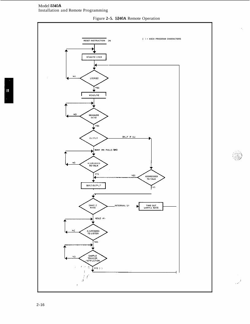
Model 534QA Installation and Remote Programming
Figure 2-5. 534QA Remote Operation
RESET INSTRUCTION IHI 1 1 I ASCII PROGRAM CHARACTERS
-1
-1 MEASURE
,LAIT IMI PULLS SRO
t
TO TALK
ADDRESSED TO TALK
INTERNAL (JI TIME OUT SAMPtE RATE
TO LISTEN
I) 1' . i
I
2-16
Model 5340A Installation and Remote Programming
2-52. The two principal niodes of remote operation based on the Sample Rate and Output modes are described in (a) and (b) below. Modes (c) and (d) are possible by selecting the remaining combinations of the Sample Rate and Output modes.
a. Internal Sample Rate (J) and Output ONLY IF (L)
(1) If NOT addressed to TALK the 5340A makes measurements continuously at a rate determined by its Sample Rate time plus measurement time. It skips the output phase of its operating cycle.
(2) If 5340A is addressed to TALK, it no longer skips its output phase. The next and all subsequent measurements are outputted.
b. Sample Rate HOLD (K) and WAIT until addressed (M) the 5340A sequence is:
(1) Addressed to LISTEN.
(2) Instructed to make a measurement.
(3) Makes a measurement and stops in its output phase. (4) Addressed to TALK.
(5) Outputs and stops in its Sample Rate phase. (6) Addressed to LISTEN.
(7) Instructed to make measurement, then repeats 3 through 6.
c. Internal Sample Rate (J) and WAIT until addressed (M) the 5340A:
(1) Makes a measurement and stops in its output phase. (2) Is addressed to TALK.
(3) Outputs, goes through its sample rate, and makes another measurement and if
(a) Still addressed to TALK it repeats (3).
(b) Not addressed to TALK it stops in its output phase and waits until so addressed then repeats (3).
d. Sample Rate HOLD (K) and Output ONLY IF addressed (L) the 5340A is:
(1) Addressed to LISTEN.
(2) Instructed to make a measurement. (3) Makes the measurement and if:
(a) Addressed to TALK by the end of the measurement phase it outputs and stops in the Sample Rate phase until (1) and (2) are repeated.
(b) Not addressed to TALK by the end of the measurement phase it skips out- put and stop in the Sample Rate phase until (1) and (2) are repeated.
2-53. Starting a Measurement Procedure
2-54. When operating the 5340A under remote control, a measurement procedure may be initiated by sending a Reset or Sample Trigger Instruction or by letting its sample rate time run out.
a.
b. Reset Instruction ( € k ) j
Internal Sample Rate;XJ) - a measurement starts at the end of sample rate time.
. I (1) Can bei given at any time during a 5340A’s operating cycle.
( 2 ) Does not change the information in the program storage cells.
2-17
Model 5340A Installation and Remote Programming
(3) Clears the display. \
) (4) Initializes the phase locked loops forcing a new search procedure.
(5) Starts measurement phase of the 5340A’s operating cycle.
c. Sample Triggers Instruction (I):
(1) Can be given only if the 5340A is stopped in the Sample Rate phase of its operating cycle. If given at any other time it will be ignored by 5340A.
(2) Does not change the information in the program storage cells.
(3) Does not clear the display.
(4) Does not initialize the phase locked loops, i.e., the 5340A does not go through a search procedure unless it has lost phase lock since the previous measurement.
(5) Starts the measurement phase of the 5340A’s operating cycle.
2-55. Examples of Programming
2-56. Assume that it is desired to program a 5340A for a measurment of approximately 3.5 GHz to a 1 kHz resolution. In addition, it is desired to instruct the 5340A to make a measurement and subsequently output when so instructed. One method of programming this is shown in Table 2-6. (Assume the 5340A listen address is ASCII “#” and the talk address is ASCII “C”.)
2-57. Another example of programming is with a mark sense card reader. Assume that it is desired to program a 5340A using a 3260A Mark Sense Programmer for an automatic measure- ment to a 1 kHz resolution (where a digital output is not required). Figure 2-6 shows the marked program card. . ., )
, , , r
2-18
‘t
i
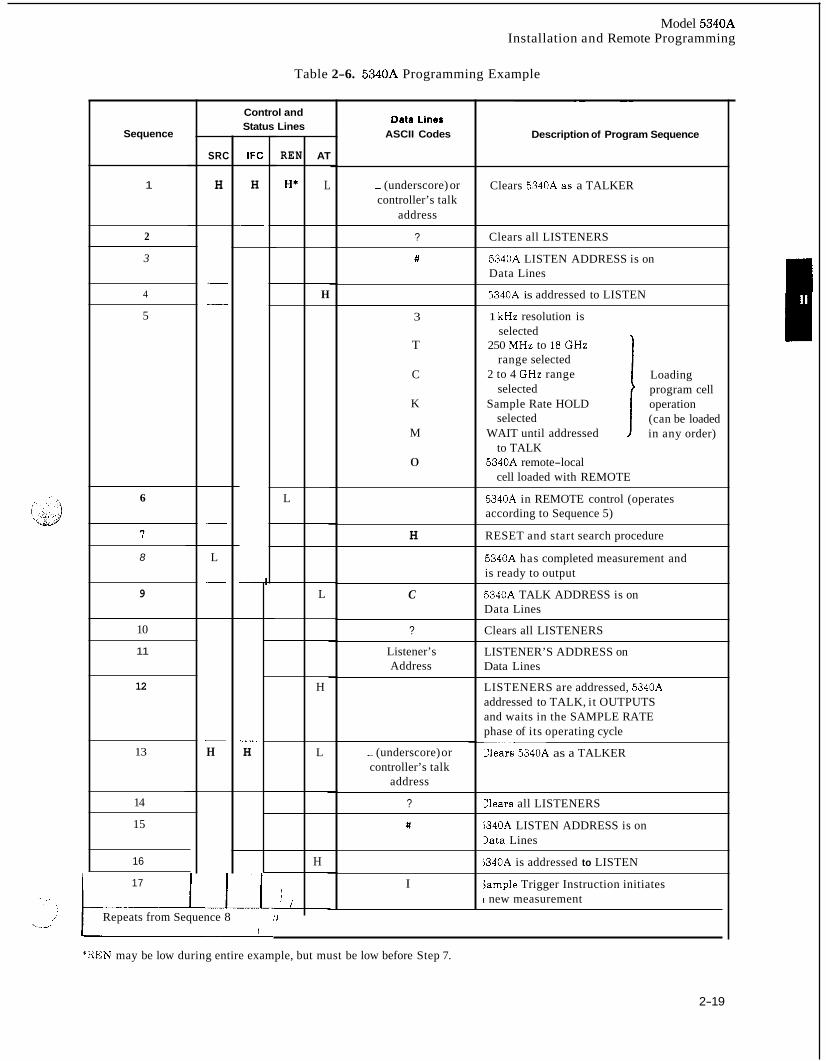
Model 5340A Installation and Remote Programming
REN
H*
L
{
i ,
Table 2-6. 5340A Programming Example
AT
L
H
L
H
L
H
~~ ~~
Description of Program Sequence
Control and Status Lines
Data Lines ASCII Codes Sequence
1
2
3
4
5
6
7
8
9
10
11
12
13
14
15
16
17
SRC IFC
H H
-
Clears 5340A as a TALKER - (underscore) or controller’s talk
address
? Clears all LISTENERS
# 5340A LISTEN ADDRESS is on Data Lines
5340A is addressed to LISTEN
1 kHz resolution is selected
250 MHz to 18 GHz range selected
2 to 4 GHz range selected
Sample Rate HOLD selected
WAIT until addressed to TALK
5340A remote-local cell loaded with REMOTE
Loading program cell operation (can be loaded I in any order)
3
T
C
K
M
0
5340A in REMOTE control (operates according to Sequence 5)
H RESET and start search procedure
L
- 5340A has completed measurement and is ready to output
~~
5340A TALK ADDRESS is on Data Lines
Clears all LISTENERS
C
?
Listener’s Address
LISTENER’S ADDRESS on Data Lines
LISTENERS are addressed, 5340A addressed to TALK, it OUTPUTS and waits in the SAMPLE RATE phase of its operating cycle -
H - H
~~
Zlears 5340A as a TALKER - (underscore) or controller’s talk
address
? Xears all LISTENERS
i340A LISTEN ADDRESS is on >ata Lines
#
i340A is addressed to LISTEN
I sample Trigger Instruction initiates L new measurement
I ,J Repeats from Sequence 8 ,i
I L-7
*REN may be low during entire example, but must be low before Step 7.
2-19
Model 534041 Installation and Remote Programming
Figure 2-6. Example Program Card
PI (0 rn 0 m N ' > + 0 0 0 _O 0 0 0 4 a o o o o o o o o
CLEARS 5340 AS A TALKER CLEARS ALL LISTENERS
5340 LISTEN ADDRESS 1 kHz RESOLUTION
AUTO RANGE INTERNAL SAMPLE RATE
OUTPUT ONLY IF ADDRESSED REMOTE
RESET CLEAR 5340 AS A LISTENER
503 & 10 HZ - 18 GHz
1. m LOW (1)
0 HIGH (0 )
2. REFER TO TABLE 2-2. 2-3, A N D 2-4 FOR PROGRAM CODES.
3. 3260A MARK SENSE PROGRAMMER SETS REN LOW A L L T H E T I M E POWER IS ON.
HADED AREA (TOP)
I ,
FOR DIGITAL/OUTPUT, ADD C AND ( ) 5340 TALK ADDRESS J
I
J ' :?
2-20
Model 5340A Operation
SECTION 111
OPERATION
3-1. INTRODUCTION
3-2. This section contains operating information including operating characteristics, input cable considerations, controls and indicators, and operating procedures. Programming instructions are contained in Section 11.
3-3. OPERATING CHARACTERISTICS
3-4. The following paragraphs describe the operating ranges and modes, resolution, sample rate, AM and FM characteristics, and auto-amplitude discrimination.
3-5. Operating Ranges
3-6. There are two basic operating ranges available: 10 Hz to 250 MHz and 250 MHz to 18 GHz. Frequencies in the lower range are measured directly while measurements in the 250 MHz to 18 GHz range are made with an indirect transfer oscillator technique. Provision is made to select three operating ranges, these are:
a. 10 Hz to 250 MHz at the BNC connector (1 MR, 25 pF).
b. 250 MHz to 18 GHz at the N connector (50R).
c. 10 Hz to 18 GHz at the N connector (50R).
3-7. The 10 Hz to 250 MHz range restricts the counter to direct measurements. The 250 MHz to 18 GHz range restricts the counter to the transfer oscillator mode, and the 10 Hz to 18 GHz range allows both modes of operation to be in effect. Annunciator lights are included to indicate when the counter is measuring directly (DIR light) or indirectly (LOCK light). It should be noted that during the 10 Hz to 18 GHz operation, the counter may lock on a signal in the 10 Hz to 250 MHz range in preference to a signal in the transfer oscillator range. Thus, to measure a high frequency signal (>250 MHz) containing high levels of residual low frequencies, it is necessary to select the 250 MHz to 18 GHz range. Otherwise, the switch position is dictated by the impedance require- ments and frequency of the input signal.
3-8. Resolution and Blanking
3-9. In a frequency counter, resolution can be defined as the value represented by the least, significant digit (LSD). In the 5340A, a maximum resolution of 1 Hz can be selected. Decade multiples of 1 Hz to 1 MHz are available. For example, with an input of 12,345,678 Hz, setting the RESOLUTION switch to 1, the counter displays the 8 in the LSD. Selecting 100 on the RESO- LUTION switch places the 6 in the LSD. If a frequency such as 123,456,789 Hz is measured with 1 Hz resolution selected, the counter will overflow so that the 1 is not displayed and the 9 will appear in the LSD. For ,high resolution of measurements which would result in an overflow, two measurements can be made.' The first measurement is made with a resolution setting that is adequate to display the mqst significant digits. The second measurement is made with maximum resolution to display the leak significant digits.
3-10. The counter blanks all digits to the left of the most significant digit, suppressing lead- ing zeros.
J I
i
3-1
Model 5340A Operation
3-11. Sample Rate, Measurement Time, and Reset
3-12. The sample rate control sets the interval between measurements, but not the interval of the measurement. On the 5340A, the minimum sample rate is variable between approximately 50 milliseconds and 5 seconds. For 1 Hz RESOLUTION settings, a n additional 1 sec delay is incurred. A hold feature can be selected to “freeze” a measurement display indefinitely.
\
3-13. The measurement interval (gate time) is the time that the counter’s gate remains open to accumulate counts. In the 5340A, the gate time is a function of the resolution selected and the input frequency. Typical measurement time for an 18 GHz signal with 1K resolution selected is about 120 msec. With 1 Hz resolution selected and an 18 GHz input, the gate time is quite long, approximately 120 seconds. However during this time, the LOCK annunciator lights to indicate that a measurement is in progress.
3-14. Reset is accomplished by pressing the RESET switch or changing the RESOLUTION or RANGE switch. When the counter is reset, the display reads all zeros and a h e w measurement cycle is initiated.
3-15. AM Characteristics
3-16. The 5340A will measure inputs containing amplitude modulation provided that the mini- mum level of the input signal is greater than the sensitivity specification. The maximum modu- lation permissible can be calculated by the following formula:
vu - vs v u = % modulation where: Vu is the unmodulated rms input level.
Vs is the sensitivity specification at the frequency of interest.
As an example of the use of the formula, calculate the maximum permissible modulation for a -10 dBm (70 mV) input at 10 GHz. At 10 GHz, the sensitivity specification is -35 dBm (4 mV) Using the formula:
Vu- Vs - 7 0 m V- 4 m V - - 66 mV = 94.5% modulation v u 70 mV 70 mV
3-17. FM Characteristics
3-18. phase modulation, or residual noise. rate and carrier frequency as shown in Figure 3-1.
The 5340A will measure carrier frequencies in the presence of frequency modulation, The FM characteristics are a function of the modulation
Figure 3-1. FM Characteristics
I I I I I 10 100 1K 10K 1 OOK 1M
1, - MODULATING FREOUENCY - Hz
3-2
'.. a low
1 w
t w
l W m W
l a n W 5mW
1mW
1ooj Iw
low
3PW
1PW
0.3jIW
a 1 g w
0.01jIw
Model 5340A Operation
- -
- -
- - - -
- - - - -
-
3-19. Auto-Amplitude Discrimination
3-20. This feature allows the counter to select and measure the signal with the largest amplitude in the 250 MHz to 18 GHz range. This is with the provision that the largest signal is 20 dB greater in amplitude than any other signal present. Although 20 dB is the guaranteed specification, typical operation is about 10 dB. The auto-amplitude discrimination feature is useful for dis- criminating against harmonics, and spurious signals.
3-21. MAXIMUM INPUT SIGNAL POWER
I CAUTION ] DO NOT EXCEED 1 WATT OF INPUT POWER AT THE
INTERNAL SAMPLERS MAY OCCUR. PLEASE READ
INPUT LEVELS.
50-OHM N CONNECTOR. DAMAGE TO THE
PARAGRAPH 3-22 FOR FULL EXPLANATION OF
3-22. The 5340A will function within specifications for signal inputs up to +7 dBm (5.012 milli- watts or 0.5006 volts into 50-ohms). Under no circumstance should the input level exceed 1-watt (+30 dBm RF power or *7 volts dc into 50-ohms, dc power). If the input power exceeds 1-watt, damage to the internal samplers may occur and these are quite expensive to replace. Measure- ments from +7 dBm to +30 dBm are not recommended because false harmonic locks and readings may occur. When signal levels exceed +7 dBm, external attenuators should be used. The 1-watt maximum input level is the total RF and dc power a t the input connector. Figure 3-2 shows power levels with conversions to volts and dBm.
Figure 3-2. DBM to Volts Conversions
POWER1 WATTS dBm
3-3
Model 5340A Operation
3-23. INPUT CABLE CONSIDERATIONS
3-24. Consideration should be given to input cable losses at higher frequencies. For example, a 6-foot RG-214/U coaxial cabIe has about 15 dB loss a t 18 GHz. Such losses should be taken into consideration along with the sensitivity specifications given in Table 1-3.
3-25. For low capacity input measurements, a 1O:l low capacity oscilloscope probe (HP 10004A) can be used on the BNC connector for frequency inputs up to approximately 100 MHz.
3-26. CONTROLS, INDICATORS, AND CONNECTORS
3-27. describes the rear panel connectors and controls.
Figure 3-3 describes the front panel controls, indicators, and connectors. Figure 3-4
3-28. OPERATING PROCEDURES
3-29. Figure 3-6.
Figure 3-5 illustrates the operating procedures. Self check procedures are givei
3-4
Model 5340A Operation
Figure 3-3. Front Panel Controls and lndicators
10 9 8 11 12 13 14 15 16
1. LINE switch. Applies primary power to all circuits except crystal oven Option 001, when so equipped. When the counter is equipped with Option 001, the crystal oven connects through a thermal circuit breaker and fuse to the ac line. This allows the oven to maintain its operating temperature and accuracy when the LINE switch is OFF, thereby eliminating warm-up delays.
2. RESET switch. measurement.
Resets display and internal count to zero and initiates a new
3. RESOLUTION Hz selector. Determines resolution of the measurement. See Paragraph 3-8 for a detailed description. In general, the 1 kHz setting is a good starting point.
SAMPLE RATE control. Adjusts the interval between measurements from ap- proximately 50 milliseconds to 5 seconds. For 1 Hz RESOLUTION settings an additional 1 second delay is incurred. When rotated to the HOLD position, the display will be held indefinitely.
BNC 1 MEG Q Input Connector. High impedance (1 Megohm) input for direct count measurements in the 10 Hz to 250 MHz range. Shunt input capacity is 25 pF maximum. Measurements made a t this input require that the RANGE switch is set to the 10 Hz - 250 MHz position. Sensitivity is 50 millivolts rms and the coupling is ac.
RANGE switch. Selects input connectors and ranges as indicated by the black leader lines. When set to the CHECK position, the circuits count the frequency of the internal clock to verify proper counter operation.
4.
5.
6.
, , I , I
DO NOT EXCE D +30 dBm (1 WATT) INPUT AT THE 500 N CONNECTOR. DAMAGE TOjT sk E INTERNAL SAMPLERS MAY OCCUR. PLEASE READ PARAGRAPH 3-21 FOR DETAILS OF ACCEPTABLE INPUT LEVELS.
3-5
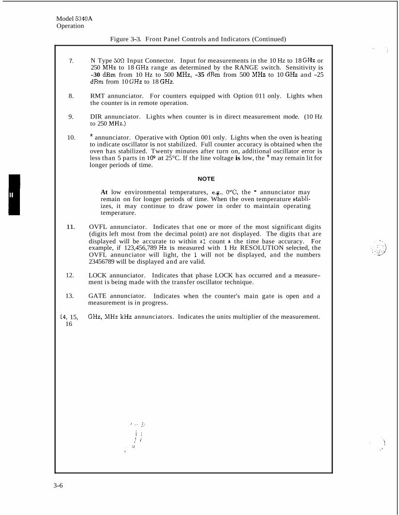
Model 5340A Operation
Figure 3-3. Front Panel Controls and Indicators (Continued)
7.
8.
9.
10.
11.
12.
13.
14, 15, 16
N Type 500 Input Connector. Input for measurements in the 10 Hz to 18 GHz or 250 MHz to 18 GHz range as determined by the RANGE switch. Sensitivity is -30 dBm from 10 Hz to 500 MHz, -35 dBm from 500 MHz to 10 GHz and -25 dBm from 10 GHz to 18 GHz.
RMT annunciator. For counters equipped with Option 011 only. Lights when the counter is in remote operation.
DIR annunciator. Lights when counter is in direct measurement mode. (10 Hz to 250 MHz.)
* annunciator. Operative with Option 001 only. Lights when the oven is heating to indicate oscillator is not stabilized. Full counter accuracy is obtained when the oven has stabilized. Twenty minutes after turn on, additional oscillator error is less than 5 parts in lo9 at 25°C. If the line voltage is low, the * may remain lit for longer periods of time.
NOTE
At low environmental temperatures, e.g., O"C, the * annunciator may remain on for longer periods of time. When the oven temperature stabli- izes, it may continue to draw power in order to maintain operating temperature.
OVFL annunciator. Indicates that one or more of the most significant digits (digits left most from the decimal point) are not displayed. The digits that are displayed will be accurate to within *1 count f the time base accuracy. For example, if 123,456,789 Hz is measured with 1 Hz RESOLUTION selected, the OVFL annunciator will light, the 1 will not be displayed, and the numbers 23456789 will be displayed and are valid.
LOCK annunciator. ment is being made with the transfer oscillator technique.
GATE annunciator. measurement is in progress.
Indicates that phase LOCK has occurred and a measure-
Indicates when the counter's main gate is open and a
GHz, MHz kHz annunciators. Indicates the units multiplier of the measurement.
3-6
Model 5340A Operation
Figure 3-4. Rear Panel Controls and Connectors
1.
2.
3.
4.
5 .
6.
7.
8.
9.
8 2 3
7 1 9 4 6 5
10 MHz OUTPUT. Supplies a 10 MHz square wave output at 2.4 volts peak-to- peak or greater. Output is TTL compatible.
INT-EXT OSC switch. Selects time base source. When set to INT, the counter operates from its internal 10 MHz oscillator. When set to EXT, it allows an external 10 MHz sine wave or square wave at the 10 MHz INPUT jack to operate the counter. External oscillator requirements are 10 MHz at approximately 1.5 volts peak-to-peak into 1 kR.
10 MHz INPUT jack. Accepts external time base signal. Requirements are a 10 MHz sine wave or square wave at approximately 1.5 volts peak-to-peak (1 kR impedance). The INT-EXT switch must be set to EXT to accept the external OSC input.
AC Input Connector. Ac power receptacle. IEC type with offset pin connected to the chassis. Accepts 115 volts or 230 votls *lo%, 48 to 68 Hz. Maximum power draw is 100 volt amperes.
SELECTOR switch. Allows the 5340A to operate off of 115 volts or 230 volts ac. Use a narrow bladed screwdriver and slide the switch to show the desired oper- ating voltage.
FUSE. Requires a 2.0 amp normal blow fuse for 115-volt operation or a 1.0 amp normal blow fuse for 230-volt operation.
Input Option 002 N connector. Same as front panel N connector, see Figure 3-3.
BNC input connector Option 002. Similar to front panel BNC input except that this optiod ihdhdes a 50-ohm termination on the front panel BNC connector.
Digital InpdtfOutput Option 011. programmihg and digital output. See Section I1 for details of operation.
Connector and address switches for remote
1
3-7
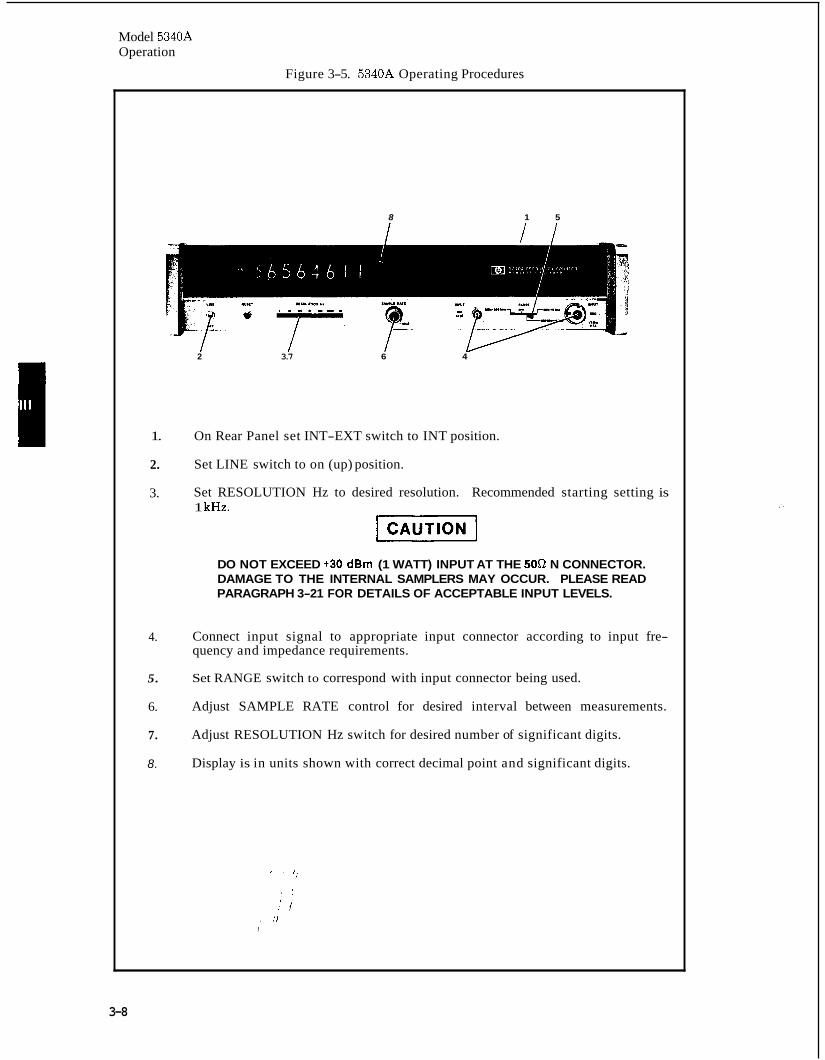
Model 5340A Operation
Figure 3-5. 5340A Operating Procedures
1.
2.
3.
4.
5.
6.
7.
8.
8 1 5
2 3.7 6 4
On Rear Panel set INT-EXT switch to INT position.
Set LINE switch to on (up) position.
Set RESOLUTION Hz to desired resolution. Recommended starting setting is 1 kHz.
DO NOT EXCEED t30 dBm (1 WATT) INPUT AT THE 50Q N CONNECTOR. DAMAGE TO THE INTERNAL SAMPLERS MAY OCCUR. PLEASE READ PARAGRAPH 3-21 FOR DETAILS OF ACCEPTABLE INPUT LEVELS.
Connect input signal to appropriate input connector according to input fre- quency and impedance requirements.
Set RANGE switch to correspond with input connector being used.
Adjust SAMPLE RATE control for desired interval between measurements.
Adjust RESOLUTION Hz switch for desired number of significant digits.
Display is in units shown with correct decimal point and significant digits.
3-8
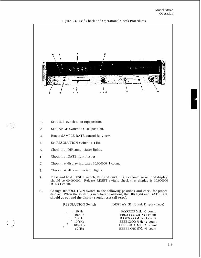
Model 5340A Operation
Figure 3-6. Self Check and Operational Check Procedures
7 8 - -
/ I . ‘ I I \ \ \
1.
2.
3.
4.
5.
6.
7.
8.
9.
10.
I 1 9’ 4 , l O 3.1 i.12 13 2 15
Set LINE switch to on (up) position.
Set RANGE switch to CHK position.
Rotate SAMPLE RATE control fully ccw.
Set RESOLUTION switch to 1 Hz.
Check that DIR annunciator lights.
Check that GATE light flashes.
Check that display indicates 10.000000 *1 count.
Check that MHz annunciator lights.
Press and hold RESET switch, DIR and GATE lights should go out and display should be 00.000000. Release RESET switch, check that display is 10.000000 MHz * l count.
Change RESOLUTION switch to the following positions and check for proper display. When the switch is in between positions, the DIR light and GATE light should go out and the display should reset (all zeros).
RESOLUTION Switch DISPLAY (B Blank Display Tube)
10 Hz 100 Hz
’ l k H z ’ i 10kHz ’’ 100 kHz
1 MHz
’ ;!
I
B1O.OOOOO MHz * l count BB1O.OOOO MHz *1 count BBB1O.OOO MHz *l count BBBB1O.OO MHz *1 count BBBBB1O.O MHz *1 count BBBBB.O1O GHz *1 count
3-9
I
Model 5340A Operation
Figure 3-6. Self Check and Operational Check Procedures (Continued)
11.
12.
13.
14.
15.
16.
17.
18.
19.
For the 1 MHz RESOLUTION setting, check that GATE light flashes rapidly. Rotate SAMPLE RATE control fully clockwise but not in HOLD. Gate light should flash once approximately every 5 seconds.
Set SAMPLE RATE to HOLD and check that GATE light goes out and display is held indefinitely.
Connect a 220 MHz signal at 0 dBm (0.2236 volts rms) to the 10 Hz - 250 MHz INPUT. Set RANGE switch to 10 Hz to 250 MHz. Set RESOLUTION switch to 1K. Rotate SAMPLE RATE control fully ccw.
Check that gate lamp flashes, DIR lamp lights, and counter displays proper frequency for all positions of RESOLUTION switch.
Connect the 220 MHz signal (0 dBm) to the 50Q INPUT and set RANGE switch to 10 Hz - 18 GHz. Set RESOLUTION switch to 1 kHz.
Check that GATE lamp flashes, DIR lamp lights, and counter displays correct frequency for all positions of the RESOLUTION switch.
Set RANGE switch to 250 MHz - 18 GHz. Check that LOCK lamp lights, GATE lamp flashes, and counter displays correct frequency for all positions of the RESOLUTION switch.
For each position of the RESOLUTION switch, move RANGE switch between “250 MHz - 18 GHz” and “10 Hz - 18 GHz” positions. The displayed frequencies should agree within 1 count.
If counter fails in any of the above steps, refer to Section V.
3-10
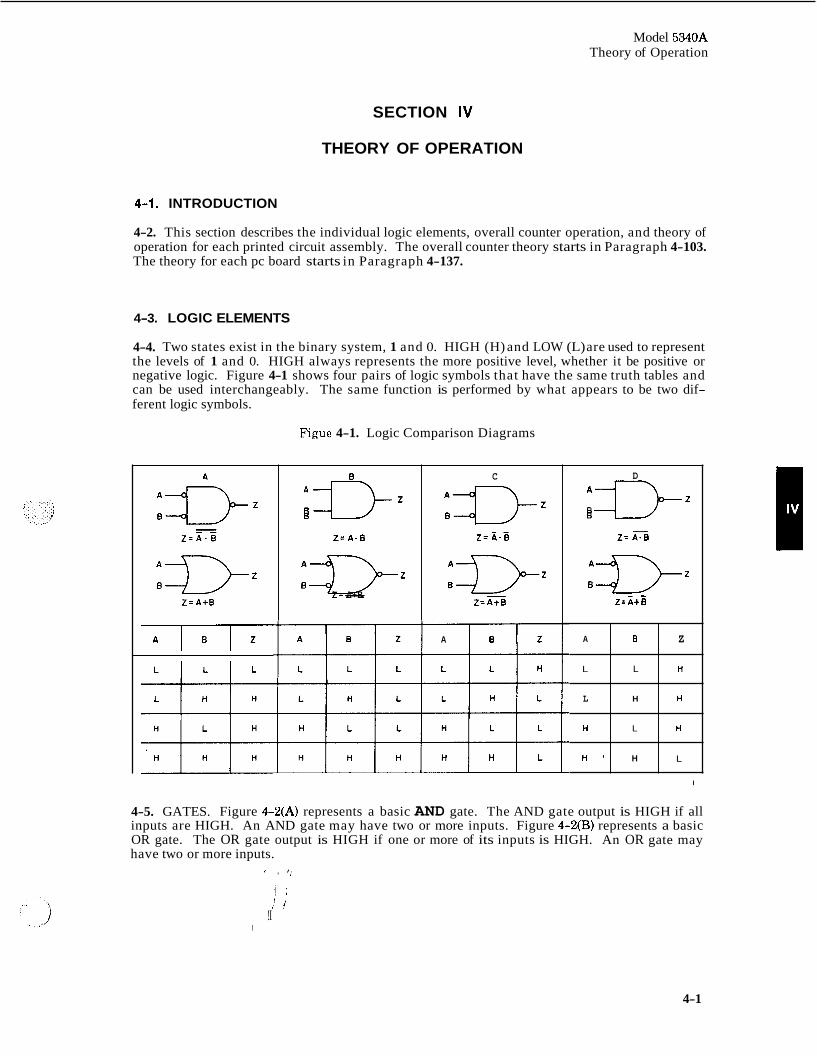
Model 5340A Theory of Operation
A B
L L
L H
H L
H a H
SECTION IV
THEORY OF OPERATION
Z
H
H
H
L
4-1. INTRODUCTION
4-2. This section describes the individual logic elements, overall counter operation, and theory of operation for each printed circuit assembly. The overall counter theory starts in Paragraph 4-103. The theory for each pc board starts in Paragraph 4-137.
4-3. LOGIC ELEMENTS
4-4. Two states exist in the binary system, 1 and 0. HIGH (H) and LOW (L) are used to represent the levels of 1 and 0. HIGH always represents the more positive level, whether it be positive or negative logic. Figure 4-1 shows four pairs of logic symbols that have the same truth tables and can be used interchangeably. The same function is performed by what appears to be two dif- ferent logic symbols.
Figue 4-1. Logic Comparison Diagrams
plslz
B
A€)-z B
Z= A . B
B+L! Z = A+B
I
C
- - Z= A . B
Z = A + B
A B z
~
D "DZ B
Z= A T 0
z- 3it B
4-5. GATES. Figure 4-2(A) represents a basic AND gate. The AND gate output is HIGH if all inputs are HIGH. An AND gate may have two or more inputs. Figure 4-2(B) represents a basic OR gate. The OR gate output is HIGH if one or more of its inputs is HIGH. An OR gate may have two or more inputs.
/ , 1 ;
!I 1
4-1
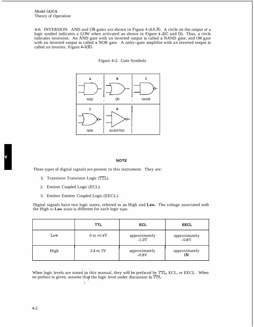
Model 5430A Theory of Operation
TTL
Low 0 to +0.4V
4-6. INVERSION. AND and OR gates are shown in Figure 4-2(A,B). A circle on the output of a logic symbol indicates a LOW when activated as shown in Figure 4-2(C and D). Thus, a circle indicates inversion. An AND gate with an inverted output is called a NAND gate; and OR gate with an inverted output is called a NOR gate. A unity-gain amplifier with a n inverted output is called an inverter, Figure 4-2(E).
ECL EECL
approximately approximately -1.5V -0.6V
Figure 4-2. Gate Symbols
High
AND OR NAND
2.4 to 5V approximately approximately -0.w ov
D E
NOR I INVERTER I
NOTE
Three types of digital signals are present in this instrument. They are:
1. Transistor Transistor Logic (WL).
2. Emitter Coupled Logic (ECL).
3. Emitter Emitter Coupled Logic (EECL).
Digital signals have two logic states, referred to as High and Low. The voltage associated with the High or Low state is different for each logic type.
When logic levels are stated i,n this manual, they will be prefaced by 'M'L, ECL, or EECL. When no preface is given, assume tha the logic level under discussion is "L. f
i
4-2
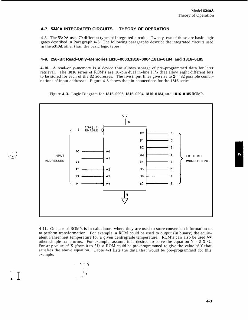
,- . I -’-
Model 5340A Theory of Operation
4-7. 5340A INTEGRATED CIRCUITS - THEORY OF OPERATION
4-8. The 5340A uses 70 different types of integrated circuits. Twenty-two of these are basic logic gates described in Paragraph 4-3. The following paragraphs describe the integrated circuits used in the 5340A other than the basic logic types.
4-9. 256-Bit Read-Only-Memories 1816-0003,1816-0004,1816-0184, and 1816-0185
4-10. A read-only-memory is a device that allows storage of pre-programmed data for later retrieval. The 1816 series of ROM’s are 16-pin dual in-line IC’s that allow eight different bits to be stored for each of the 32 addresses. The five input lines give rise to 2 5 = 32 possible combi- nations of input addresses. Figure 4-3 shows the pin connections for the 1816 series.
Figure 4-3. Logic Diagram for 1816-0003, 1816-0004, 1816-0184, and 1816-0185 ROM’s
INPUT
ADDRESSES
(15-4 ENABLE BO I-- 1
I l o 1 1 I:T 84 B3 I: EIGHT-BIT ’ WORD OUTPUT
4-11. One use of ROM’s is in calculators where they are used to store conversion information or to perform transformation. For example, a ROM could be used to output (in binary) the equiv- alent Fahrenheit temperature for a given centrigrade temperature. ROM’s can also be used fok other simple transforms. For example, assume it is desired to solve the equation Y = 2 X +1. For any value of X (from 0 to 31), a ROM could be pre-programmed to give the value of Y that satisfies the above equation. Table 4-1 lists the data that would be pre-programmed for this example.
4-3
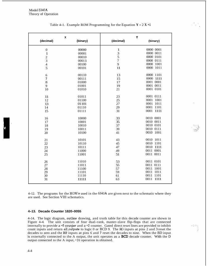
Model 5340A Theory of Operation
Table 4-1. Example ROM Programming for the Equation Y = 2 X +I
X (decimal) (binary)
0 1 2 3 4 5
6 7 8 9 10
11 12 13 14 15
16 17 18 19 20
21 22 23 24 25
26 27 28 29 30 31
00000 00001 00010 0001 1 00100 00101
00110 00111 01000 01001 01010
01011 01100 01 101 01110 01111
10000 10001 10010 10011 10100
10101 10110 10111 11000 11001
11010 11011 11100 11101 11110 11111
Y (decimal) (binary)
1 3 5 7 9 11
13 15 17 19 21
23 25 27 29 31
33 35 37 39 41
43 45 47 49 51
53 55 57 59 61 63
0000 0001 0000 0011 0000 0101 0000 0111 0000 1001 0000 1011
0000 1101 0000 1111 0001 0001 0001 0011 0001 0101
0001 0111 0001 1001 0001 1011 0001 1101 0001 1111
0010 0001 0010 0011 0010 0101 0010 0111 0010 1001
0010 1011 0010 1101 0010 1111 0011 0001 0011 0011
0011 0101 0011 0111 0011 1001 0011 1011 0011 1101 0011 1111
4-12. The programs for the ROM's used in the 5340A are given next to the schematic where they are used. See Section VIII schematics.
4-13. Decade Counter 1820-0055
4-14. The logic diagram, oukline drawing, and truth table for this decade counter are shown in Figure 4-4. The unit consists of four dual-rank, master-slave flip-flops that are connected internally to provide a +5 coun,ter and a +2 counter. Gated direct reset lines are provided to inhibit count inputs and return al1,putputs to logic 0 or BCD 9. The RO inputs at pins 2 and 3 reset the decades to zero and the R9 inputs at pins 6 and 7 reset the decades to nine. When the BD input is externally connected to the A output, the unit operates as a BCD decade counter. With the D output connected to the A input, +10 operation is obtained.
4-4
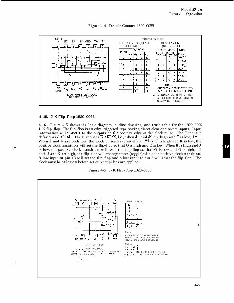
Model 5340A Theory of Operation
Figure 4-4. Decade Counter 1820-0055
INPUT TRUTH TABLES BCD COUNT SEQUENCE RESET /COUNT
(SEE NOTE 2 )
A NC ZA ZD GND ZB 'ZC (SEE NOTE I )
RO(ll 'O(21 NC "CC '9(l) R9(2) INPUT 1820-0055(SN7490N) 2. X INDICATES THAT EITHER
A LOGICAL I OR A LOGICAL 0 MAY BE PRESENT
DECADE COUNTER
4-15. J-K Flip-Flop 1820-0065
4-16. Figure 4-5 shows the logic diagram, outline drawing, and truth table for the 1820-0065 J-K flip-flop. The flip-flop is an edge-triggered type having direct clear and preset inputs. Input information will tzansfer to the outputs on t_he positive edge of the clock pulse. The J input is defined as 51.52.5. The K input is Kl.K2*K, i.e., when J1 and 52 are high and 3 is low, J = 1. When J and K are both low, the clock pulses have no effect. Whsn J is high and K is low, the positive clock transition will set the flip-flop so that Q is high and Q is low. When K i s high and J is low, the positive clock transition will reset the flip-flop so that Q is low and Q is high. If both J and K are high, the flip-flop will change states (toggle) with each positive clock transition. A low input at pin 13 will set the flip-flop and a low input to pin 2 will reset the flip-flop. The clock must be at logic 0 before set or reset pulses are applied.
Figure 4-5. J-K Flip-Flop 1820-0065
- vCC PRESET CLK K 2 K I
J - K F L I P - F L O P
, , POSITIVE LOGIC
T R U T H T A B L E
NOTE
CLOCK MUST BE AT LOGICAL 0 PRIOR TO T H E APPLICATION OF PRESET OR CLEAR FUNCTIONS
NOTES I J=JI. J2 . 1 2 K=KI, K2 ,
4 ,"+I= BIT TIME AFTER CLOCK PULSE LOW'INPUT'TO PRESET SETS o TO LOGICAL I 3 t n = B I ~ TIME BEFORE CLOCK PULSE LOW INPUT T O CLEAR SET P TO LOGICAL 0
i
4-5
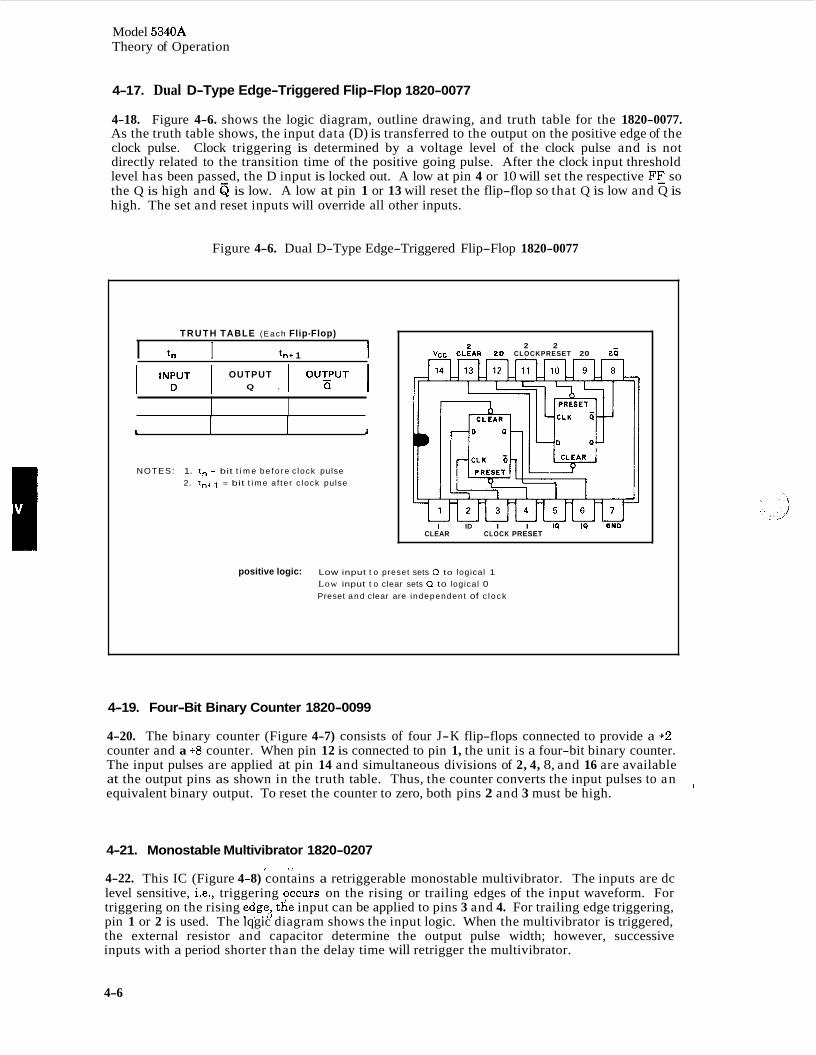
Model 5340A Theory of Operation
4-1 7. Dual D-Type Edge-Triggered Flip-Flop 1820-0077
4-18. Figure 4-6. shows the logic diagram, outline drawing, and truth table for the 1820-0077. As the truth table shows, the input data (D) is transferred to the output on the positive edge of the clock pulse. Clock triggering is determined by a voltage level of the clock pulse and is not directly related to the transition time of the positive going pulse. After the clock input threshold level has been passed, the D input is locked out. A low at pin 4 or 10 will set the respective FF_ so the Q is high and is low. A low at pin 1 or 13 will reset the flip-flop so that Q is low and Q is high. The set and reset inputs will override all other inputs.
Figure 4-6. Dual D-Type Edge-Triggered Flip-Flop 1820-0077
T R U T H TABLE (Each Flip-Flop)
I tn I t n c 1 1 OUTPUT I OUT_PUT I I "yT 1 Q . Q
1 1
NOTES: 1. tn = bit t i m e b e f o r e c lock pulse 2. t n + l = bit t i m e a f te r c lock pulse
2 2 Vcc CLEAR 2D CLOCKPRESET 20 25
I ID I I 10 I0 QND CLEAR CLOCK PRESET
positive logic: Low input t o preset sets 0 to logical 1 Low input t o clear sets 0 to logical 0 Preset a n d clear are independent of c l o c k
4-19. Four-Bit Binary Counter 1820-0099
4-20. The binary counter (Figure 4-7) consists of four J-K flip-flops connected to provide a +2 counter and a +8 counter. When pin 12 is connected to pin 1, the unit is a four-bit binary counter. The input pulses are applied at pin 14 and simultaneous divisions of 2, 4, 8, and 16 are available at the output pins as shown in the truth table. Thus, the counter converts the input pulses to an equivalent binary output. To reset the counter to zero, both pins 2 and 3 must be high.
i
4-21. Monostable Multivibrator 1820-0207
4-22. This IC (Figure 4-8) contains a retriggerable monostable multivibrator. The inputs are dc level sensitive, i.e., triggering Qccurs on the rising or trailing edges of the input waveform. For triggering on the rising edgej the input can be applied to pins 3 and 4. For trailing edge triggering, pin 1 or 2 is used. The lqgic diagram shows the input logic. When the multivibrator is triggered, the external resistor and capacitor determine the output pulse width; however, successive inputs with a period shorter than the delay time will retrigger the multivibrator.
I ,,
4-6
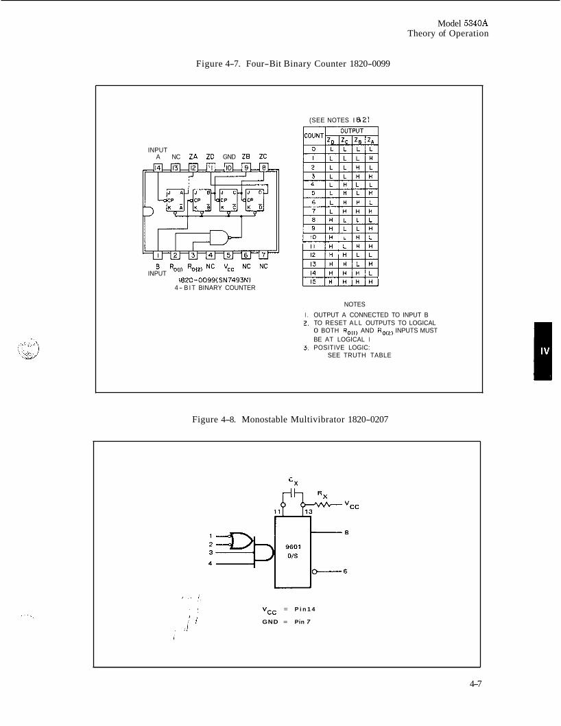
Model 5340A Theory of Operation
Figure 4-7. Four-Bit Binary Counter 1820-0099
INPUT A NC ZA ZD GND ZB ZC
B Roo, NC vcc NC NC INPUT 1820-0099(SN7493N)
4- B I T BINARY COUNTER
(SEE NOTES I a21
r*m NOTES
I . OUTPUT A CONNECTED TO INPUT B 2. TO RESET ALL OUTPUTS TO LOGICAL
0 BOTH Ro(,, AND Roo, INPUTS MUST BE AT LOGICAL I
3. POSITIVE LOGIC: SEE TRUTH TABLE
Figure 4-8. Monostable Multivibrator 1820-0207
X L
Vcc = P i n 1 4
GND = Pin 7
4-7
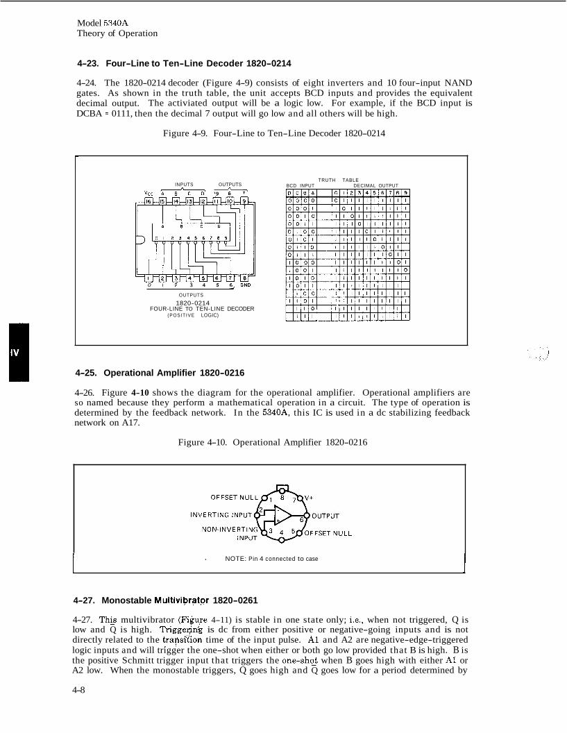
Model 5340A Theory of Operation
4-23. Four-Line to Ten-Line Decoder 1820-021 4
4-24. The 1820-0214 decoder (Figure 4-9) consists of eight inverters and 10 four-input NAND gates. As shown in the truth table, the unit accepts BCD inputs and provides the equivalent decimal output. The activiated output will be a logic low. For example, if the BCD input is DCBA = 0111, then the decimal 7 output will go low and all others will be high.
Figure 4-9. Four-Line to Ten-Line Decoder 1820-0214
r INPUTS OUTPUTS
vcc ITtf-TT ‘9 : i
0 1 2 3 4 5 6 , G N D
OUTPUTS
1820-0214
(POSIT IVE LOGIC) FOUR-LINE TO TEN-LINE DECODER
TRUTH TABLE BCD INPUT DECIMAL OUTPUT
4-25. Operational Amplifier 1820-0216
4-26. Figure 4-10 shows the diagram for the operational amplifier. Operational amplifiers are so named because they perform a mathematical operation in a circuit. The type of operation is determined by the feedback network. In the 5340A, this IC is used in a dc stabilizing feedback network on A17.
Figure 4-10. Operational Amplifier 1820-0216
1 . NOTE: Pin 4 connected to case I 4-27. Monostable Multiviprator 1820-0261
4-27. This multivibrator (Fi$uie 4-11) is stable in one state only; i.e., when not triggered, Q is low and Q is high. Triggerink is dc from either positive or negative-going inputs and is not directly related to the transidion time of the input pulse. A1 and A2 are negative-edge-triggered logic inputs and will trigger the one-shot when either or both go low provided that B is high. B is the positive Schmitt trigger input that triggers the one-sh$ when B goes high with either A1 or A2 low. When the monostable triggers, Q goes high and Q goes low for a period determined by
4-8
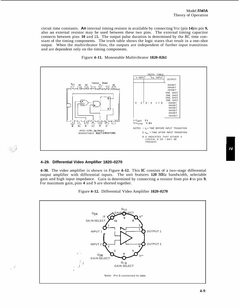
Model 5340A Theory of Operation
X O O X l O
circuit time constants. An internal timing resistor is available by connecting Vcc (pin 14) to pin 9, also an external resistor may be used between these two pins. The external timing capacitor connects between pins 10 and 11. The output pulse duration is determined by the RC time con- stant of the timing components. The truth table shows the logic states that result in a one-shot output. When the multivibrator fires, the outputs are independent of further input transitions and are dependent only on the timing components.
Figure 4-11. Monostable Multivibrator 1820-0261
TIMING PINS 'CC NC NC ,-fi-, NC
TRUTH TABLE 'n INPUT ' n t i INPUT
OUTPUT
INHIBIT INHIBIT INHIBIT
ONE SHOT ONE SHOT ONE SHOT ONE SHOT
INHIBIT INHIBIT INHIBIT INHIBIT INHIBIT I N H I B I T
b NC A l A 2 B 0 NOTES I 1 , = TIME BEFORE INPUT TRANSITION
2 I n + , = TIME AFTER INPUT TRANSITION
3 X INDICATES THAT EITHER A
1820- 0261 ~SN741213 MONOSTABLE MULTIVIBRATORS
LOGICAL 0 OR I MAY BE PRESENT
4-29. Differential Video Amplifier 1820-0270
4-30. The video amplifier is shown in Figure 4-12. This IC consists of a two-stage differential output amplifier with differential inputs. The unit features 120 MHz bandwidth, selectable gain and high input impedance. Gain is determined by connecting a resistor from pin 4 to pin 9. For maximum gain, pins 4 and 9 are shorted together.
Figure 4-12. Differential Video Amplifier 1820-0270
G1 A GAIN SELECT
GA . IN G2A SELECT p+ INPUT 1
INPUT 2
G2B G A I N SELECT
I-
G l B GAIN SELECT
Note: P in 5 connected to case.
OUTPUT 1
OUTPUT 2
4-9
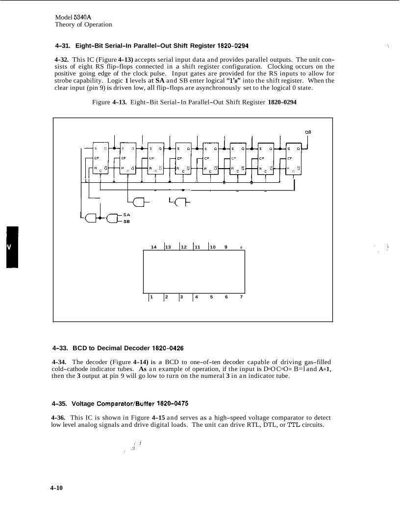
Model 5340A Theory of Operation
L
4-31. Eight-Bit Serial-In Parallel-Out Shift Register 1820-0294
4-32. This IC (Figure 4-13) accepts serial input data and provides parallel outputs. The unit con- sists of eight RS flip-flops connected in a shift register configuration. Clocking occurs on the positive going edge of the clock pulse. Input gates are provided for the RS inputs to allow for strobe capability. Logic 1 levels at SA and SB enter logical “1’s” into the shift register. When the clear input (pin 9) is driven low, all flip-flops are asynchronously set to the logical 0 state.
I A - I - 1 A 1 A I A 1 1 I 1 - - - - - I - -
Figure 4-13. Eight-Bit Serial-In Parallel-Out Shift Register 1820-0294
14 13 12 11 10 9 8
1 2 3 4 5 6 7
4-33. BCD to Decimal Decoder 1820-0426
4-34. The decoder (Figure 4-14) is a BCD to one-of-ten decoder capable of driving gas-filled cold-cathode indicator tubes. As a n example of operation, if the input is D=O C=O = B=l and A=l, then the 3 output at pin 9 will go low to turn on the numeral 3 in a n indicator tube.
4-35. Voltage Comparator/Buffer 1820-0475
4-36. This IC is shown in Figure 4-15 and serves as a high-speed voltage comparator to detect low level analog signals and drive digital loads. The unit can drive RTL, DTL, or ?TL circuits.
4-10
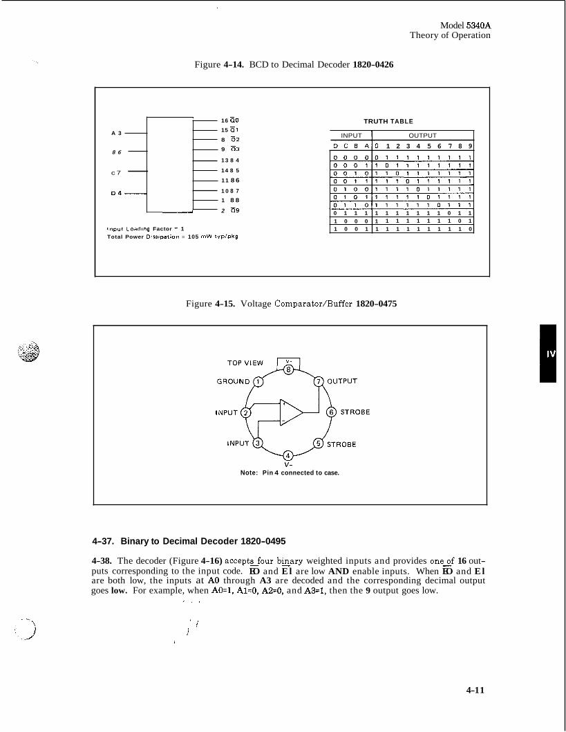
Model 5340A Theory of Operation
A 3
8 6 -
c 7 - D 4 -
Figure 4-14. BCD to Decimal Decoder 1820-0426
- 16 50 15 El 8 5 2
9 a3 1 3 8 4
14 8 5
1 1 8 6
1 0 8 7
1 8 8 - 2 a9 1 0 0 0 1
Input Loadlng Factor = 1 Total Power DissiDation = 105 m W typ lpkg
0 1 1 1 1 1 1 1 1 1 1 0 1 1 1 1 1 1 1 1 1 0 1
1 0 0 1 1 1 1 1 1 1 1 1 1 0
TRUTH TABLE
INPUT 1 OUTPUT
D C B A I O 1 2 3 4 5 6 7 8 9 0 0 0 0 0 1 1 1 1 1 1 1 1 1
0 0 1 0 1 1 0 1 1 1 1 1 1 1 0 0 1 1 1 1 1 0 1 1 1 1 1 0 1 0 0 1 1 1 1 0 1 0 1 0 1 1 1 1 1 1 0 1 1 0 1 1 0 1 1 1 1 1 1 0 1 1
31
Figure 4-15. Voltage Comparator/Buffer 1820-0475
V- Note: Pin 4 connected to case.
4-37. Binary to Decimal Decoder 1820-0495
4-38. The decoder (Figure 4-16) acceptsfour bikary weighted inputs and provides oneof 16 out- puts corresponding to the input code. EO and E l are low AND enable inputs. When EO and E l are both low, the inputs at A0 through A3 are decoded and the corresponding decimal output goes low. For example, when AO=l, A1=0, A2=0, and A3=1, then the 9 output goes low.
, ,
i I
4-1 1
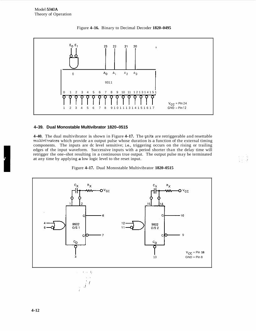
Model 5340A Theory of Operation
Figure 4-16. Binary to Decimal Decoder 1820-0495
(j 2 1 2 1 2 1 2 1 ,
I E A0 A1 A2 A3
931 1
0 1 2 3 4 5 6 7 8 9 10 11 1 2 1 3 1 4 1 5 1
Vcc = Pin 24 1 2 3 4 5 6 7 8 9 1 0 1 1 1 3 1 4 1 5 1 6 1 7 GND = Pin 12
4-39. Dual Monostable Multivibrator 1820-0515
4-40. The dual multivibrator is shown in Figure 4-17. The p i t s are retriggerable and resettable multivibrators which provide a n output pulse whose duration is a function of the external timing components. The inputs are dc level sensitive; i.e., triggering occurs on the rising or trailing edges of the input waveform. Successive inputs with a period shorter than the delay time will retrigger the one-shot resulting in a continuous true output. The output pulse may be terminated at any time by applying a low logic level to the reset input.
Figure 4-17. Dual Monostable Multivibrator 1820-0515
at-to
13
9
Vcc = Pin 16
GND = Pin 8
4-12
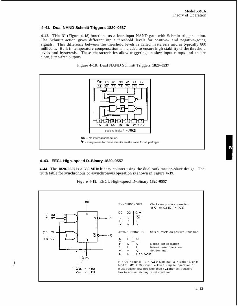
Model 5340A Theory of Operation
4-41. Dual NAND Schmitt Triggers 1820-0537
4-42. This IC (Figure 4-18) functions as a four-input NAND gate with Schmitt trigger action. The Schmitt action gives different input threshold levels for positive- and negative-going signals. This difference between the threshold levels is called hysteresis and is typically 800 millivolts. Built in temperature compensation is included to ensure high stability of the threshold levels and hysteresis. These characteristics allow triggering on slow input ramps and ensure clean, jitter-free outputs.
Figure 4-18. Dual NAND Schmitt Triggers 1820-0537
'CC 2D 2C NC 26 2A 2 Y
positive logic: Y = ABCD
NC - No internal connection.
tPin assignments for these circuits are the same for all packages.
4-43. EECL High-speed D-Binary 1820-0557
4-44. The 1820-0557 is a 350 MHz binary counter using the dual rank master-slave design. The truth table for synchronous or asynchronous operation is shown in Figure 4-19.
Figure 4-19. EECL High-speed D-Binary 1820-0557
(8) SYNCHRONOUS: Clocks on positive transition
of C1 or C2 (C1 + C2)
X H
ASYNCHRONOUS: Sets or resets on positive transition
Normal set operation Normal reset operation Set dominant
H = OV Nominal L = -0.6V Nominal X = Either L or H NOTE: must transfer low not later than t sd after set transfers low t o ensure latching in set condition.
(C1 + C2) must be low during set operation or
4-13
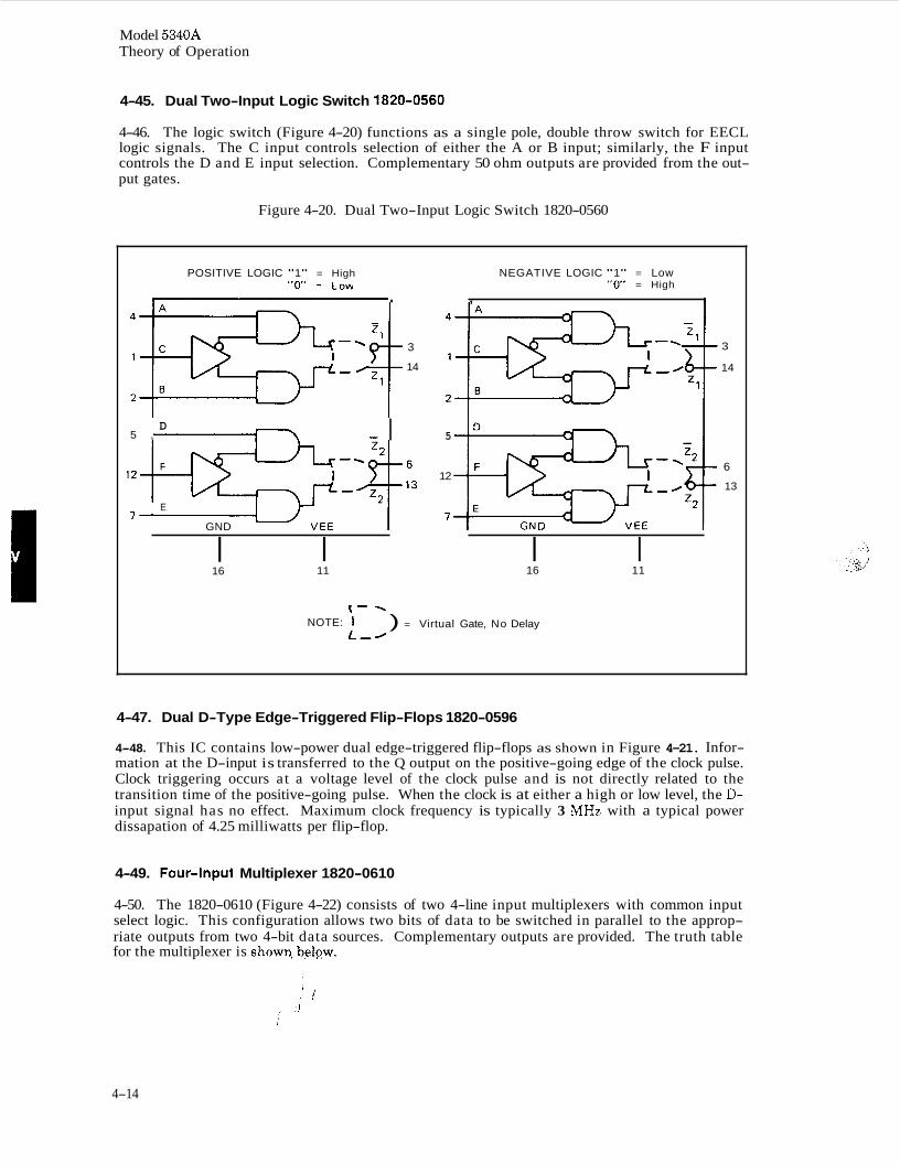
Model 5340A Theory of Operation
4-45. Dual Two-Input Logic Switch 1820-0560
4-46. The logic switch (Figure 4-20) functions as a single pole, double throw switch for EECL logic signals. The C input controls selection of either the A or B input; similarly, the F input controls the D and E input selection. Complementary 50 ohm outputs are provided from the out- put gates.
Figure 4-20. Dual Two-Input Logic Switch 1820-0560
POSITIVE LOGIC "1" = High "0" = Low .
3
14
I D 5 , -
E 7
GND
NEGATIVE LOGIC "1" = Low "0" = High
, 1
5
12
7
3
14
6
13
I 16
I 11
< - 1
I I 16 11
NOTE: ) = Virtual Gate, No Delay L , /
4-47. Dual D-Type Edge-Triggered Flip-Flops 1820-0596
4-48. This IC contains low-power dual edge-triggered flip-flops as shown in Figure 4-21. Infor- mation at the D-input is transferred to the Q output on the positive-going edge of the clock pulse. Clock triggering occurs at a voltage level of the clock pulse and is not directly related to the transition time of the positive-going pulse. When the clock is at either a high or low level, the D- input signal has no effect. Maximum clock frequency is typically 3 MHz with a typical power dissapation of 4.25 milliwatts per flip-flop.
4-49. Four-Input Multiplexer 1820-0610
4-50. The 1820-0610 (Figure 4-22) consists of two 4-line input multiplexers with common input select logic. This configuration allows two bits of data to be switched in parallel to the approp- riate outputs from two 4-bit data sources. Complementary outputs are provided. The truth table for the multiplexer is show9 belpw.
4-14
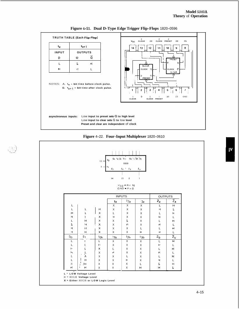
Model 5340A Theory of Operation
tn
I N P U T
D
L
H
Figure 4-21. Dual D-Type Edge Trigger Flip-Flops 1820-0596
tn+ 1
OUTPUTS
Q 0
L H
H L
-
T R U T H TABLE (Each Fl ipFlop)
1 3 -
3 -
I
so ' O a l a Z a ' 3 a i Ob'lb'21>'31>
9309
Sl 2, =a ' ZI, Zb
NOTES: A. t, = bit t i m e before c lock pulse.
6. t ,+ l = bit t i m e after clock pulse.
12a X X X X L H X X
12b X X X X L H X X
2 2 2 Vcc CLEAR 2 0 CLOCK PRESET 2 0 25
13a X X X X X X L H
I 3b X X X X X X L H
t
L A
t ,
I H /I /H I H
CLOCK a CLOCK 8
PRESET
X X X X X
I 1 1 I I
- 1 10 1 I 10 10 GND
CLEAR CLOCK PRESET
asynchronous inputs: Low input to preset sets 0 to high level Low input to clear sets 0 to low level Preset and clear are independent of clock
Figure 4-22. Four-Input Multiplexer 1820-0610
14 15 2 1
INPUTS
L L H H L L H H
SO L L H H L L H H 7
II
I l a X X L H X X X X
I l b X X L H X X X X -
L = L O W Vol tage Leve l H = H I G H Voltage Leve l X = Ei ther H I G H or L O W Logic Leve l
OUTPUTS
Za L H L H L H L H
zb L H L H L H L H
-- - za H L. H L H L H
L
zb H L H L H L H L
-
4-15
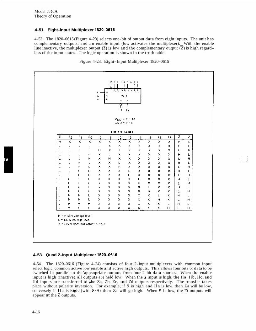
Model 5340A Theory of Operation
4-51. Eight-lnput Multiplexer 1820-0615
4-52. The 1820-0615 (Figure 4-23) selects one-bit of output data from eight inputs. The unit has complementary outputs, and a n enable input (low activates the multiplexer). - With the enable line inactive, the multiplexer output (Z) is low and the complementary output (Z) is high regard- less of the input states. The logic operation is shown in the truth table.
Figure 4-23. Eight-Input Multiplexer 1820-0615
4-53. Quad 2-Input Multiplexer 1820-0616
4-54. The 1820-0616 (Figure 4-24) consists of four 2-input multiplexers with common input select logic, common active low enable and active high outputs. This allows four bits of data to be switched in parallel to the’appsopriate outputs from four 2-bit data sources. When the enable input is high (inactive), all outputs are held low. When the S input is high, the I la , Ilb, Ilc, and I ld inputs are transferred t6 $he Za, Zb, Zc, and Zd outputs respectively. The transfer takes place without polarity inversion. For example, if S is high and Ila is low, then Za will be low, conversely if I l a is high1 (with S=H) then Za will go high. When S is low, the I0 outputs will appear at the Z outputs.
4-16
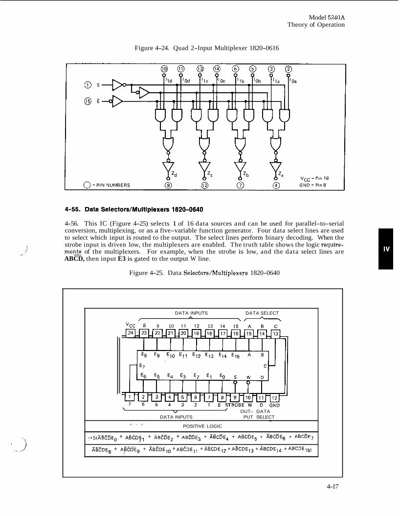
Model 5340A Theory of Operation
Figure 4-24. Quad 2-Input Multiplexer 1820-0616
I
4-56. This IC (Figure 4-25) selects 1 of 16 data sources and can be used for parallel-to-serial conversion, multiplexing, or as a five-variable function generator. Four data select lines are used to select which input is routed to the output. The select lines perform binary decoding. When the strobe input is driven low, the multiplexers are enabled. The truth table shows the logic require- men? of the multiplexers. For example, when the strobe is low, and the data select lines are ABCD, then input E3 is gated to the output W line.
Figure 4-25. Data Selectors/Multiplexers 1820-0640
DATA INPUTS DATA SELECT /
A \-
"CC 8 9 10 11 12 13 14 15 A R c
\ v / OUT- DATA DATA INPUTS PUT SELECT
~
POSITIVE LOGIC , I
, = S ( A B C D E ~ + A B C E ~ ~ + A B C D E ~ + A B C D E ~ + ABcEE, + A B C D E ~ + ABCDE, + ABCDE,
XBCDE, + A,@cD'E, + A B C D E , ~ + ABCDE,, + fiBCDEIZ + ABCDE13 + ABCDE14 + ABCDE15)
4-17
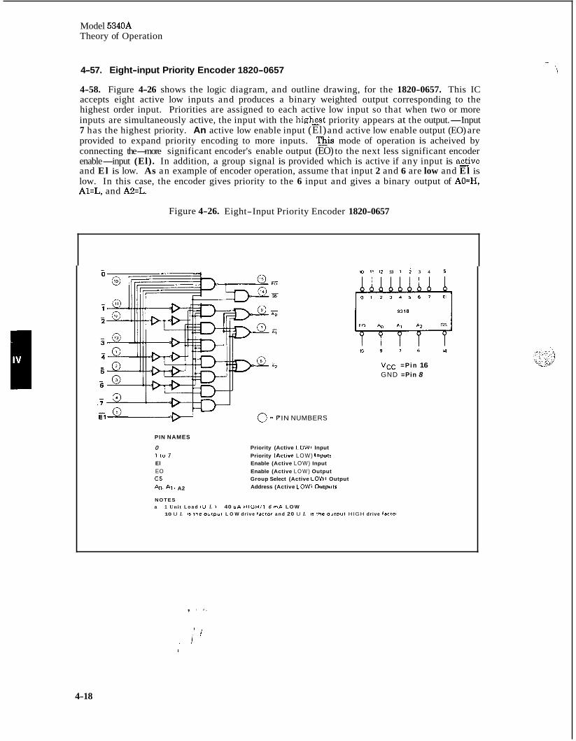
Model 5340A Theory of Operation
- 4-57. Eight-input Priority Encoder 1820-0657 1
4-58. Figure 4-26 shows the logic diagram, and outline drawing, for the 1820-0657. This IC accepts eight active low inputs and produces a binary weighted output corresponding to the highest order input. Priorities are assigned to each active low input so that when two or more inputs are simultaneously active, the input with the highest priority appears at the output.-Input 7 has the highest priority. An active low enable input (El) and active low enable output (EO) are provided to expand priority encoding to more inputs. "&is mode of operation is acheived by connecting the-more significant encoder's enable output (EO) to the next less significant encoder enable-input (El). In addition, a group signal is provided which is active if any input is active and El is low. As an example of encoder operation, assume that input 2 and 6 are low and El is low. In this case, the encoder gives priority to the 6 input and gives a binary output of AO=H, Al=L, and A2=L.
Figure 4-26. Eight-Input Priority Encoder 1820-0657
PIN NAMES
0
El EO G5
1 1 0 7
b. A1 1 A2
Priority (Active LOW1 Input Priority (Actlve LOW) Inputs Enable (Active LOW) Input Enable (Active L O W ) Output Group Select (Active LOW1 Output Address (Active LOW) Outpuls
I0 1 1 1 2 13 1 2 3 4 5
1 5 9 7 6 14
Vcc =Pin 16 GND =Pin 8
'IN NUMBERS
NOTES a 1 Unit L o a d IU L I 40 P A H I G H / l 6 m A L O W
10 U L IS the o u t ~ u 1 L O W d r i v e factor a n d 20 U L I S the O U ~ P U ~ HIGH dr ive fact08
, I I ,
4-18
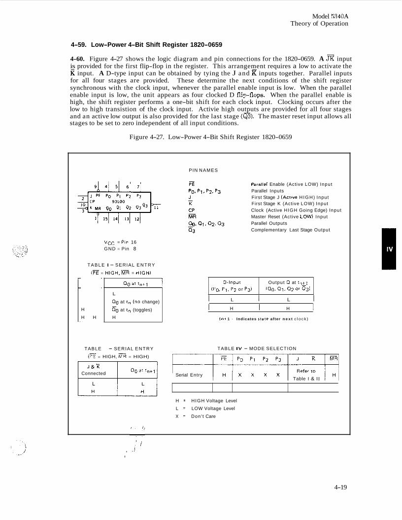
Model 5340A Theory of Operation
D-Input (Po, PI, P2 or Pgl
4-59. Low-Power 4-Bit Shift Register 1820-0659
4-60. Figure 4-27 shows the logic diagram and pin connections for the 1820-0659. A JK input is provided for the first flip-flop in the register. This arrangement requires a low to activate the
inputs together. Parallel inputs for all four stages are provided. These determine the next conditions of the shift register synchronous with the clock input, whenever the parallel enable input is low. When the parallel enable input is low, the unit appears as four clocked D fli?-flops. When the parallel enable is high, the shift register performs a one-bit shift for each clock input. Clocking occurs after the low to high transistion of the clock input. Activie high outputs are provided for all four stages and an active low output is also provided for the last stage (m). The master reset input allows all stages to be set to zero independent of all input conditions.
input. A D-type input can be obtained by tying the J and
Output 0 at t n t 1 IQo. 0 1 . 0 2 or E3)
Figure 4-27. Low-Power 4-Bit Shift Register 1820-0659
PIN NAMES
9 3 L O O
K MR QO 91 Qz 93
V c c = Pln 16 GND = Pin 8
T A B L E I - SERIAL E N T R Y
(iiT = HIGH.MR = HIGH)
H
H H
TABLE
L
Qo at tn (no change)
50 at tn (toggles)
H
- SERIAL E N T R Y
(PE = HIGH, MR = HIGH)
J E T Connected
Parallel Enable (Active LOW) Input Parallel Inputs First Stage J (Active H I G H ) Input First Stage K (Active LOW) Input Clock (Active H IGH Going Edge) Input Master Reset (Active LOW1 Input Parallel Outputs Complementary Last Stage Output
I L I L I I H I H I
( n i 1 - Indicates s f a t e after n e x t c l o c k )
TABLE IV - MODE SELECTION
Table I & I1 Serial Entry
H = H IGH Voltage Level
L = LOW Voltage Level
X = Don' t Care
, :J I
4-19
Model 5340A Theory of Operation
4-61. Low-Power BCD Decade Counter 1820-0669
4-62. Figure 4-28 shows the logic diagram and pin connections for the 1820-0669. The counter is fully synchronous with the clock pulse driving four master/slave flip-flops in parallel through a clock buffer. During the low to high clock transition, the master is inhibited from further change. After the masters are locked out, data is transferred from the master to the slaves and reflected at the outputs. When the clock is high, the masters are inhibited and the master/slave data path remains established. During the high to low transition of the clock, the slave is in- hibited from further change, followed by the enabling of the masters forthe acceptance of data from the counting logic or the parallel entry logic. The control inputs, PE, CEP, and CET, select the operating mode as shown in the tables below. During the count mode, the rising edge of the clock changes the counters to the next state of count sequence shown in the state diagram below.
4-63. m e n PE is low, the unit can be synchronously preset from the four parallel inputs PO - P3. When PE and the clock are low, each master of the flip-flops is connected to the appropriate parallel input and the slaves are steady in their previous state. When the clock goes high, the masters are inhibited and the information is tranferred to the slaves and reflected at the outputs. The parallel enable input overrides both count enable inputs, presetting the counter when low.
4-64. Terminal count is high when the counter is at terminal count (state 9), and CET is high. Without using additional logic, multistage synchronous counting at high speeds is possible with a high speed look-ahead technique. The asynchronous master reset (active low) overrides all other inputs to reset the four outputs low.
4-65. Five-Bit Comparator 1820-0706
4-66. This IC (Figure 4-29) is a high-speed expandable comparator which compares two 5-bit words to give one of three outputs: “equal to”, “less than”, or “greater than”. An active low enable line is provided to enable the comparator function. When the enable line is high, all three outputs are held low. For words containing more than &bits, comparators can be connected in series by respectively connecting the A>B and A<B outputs of the first comparator to the A0 and BO inputs of the next comparator. The truth table shows the logic operation.
4-67. Low-Power Quad Two-Input Multiplexer 1820-0710
4-68. The multiplexer consists of four multiplexing circuits with common select and enable logic. Each circuit contains two inputs and one output. The logic symbol and truth table are shown in Figure 4-30.
4-20
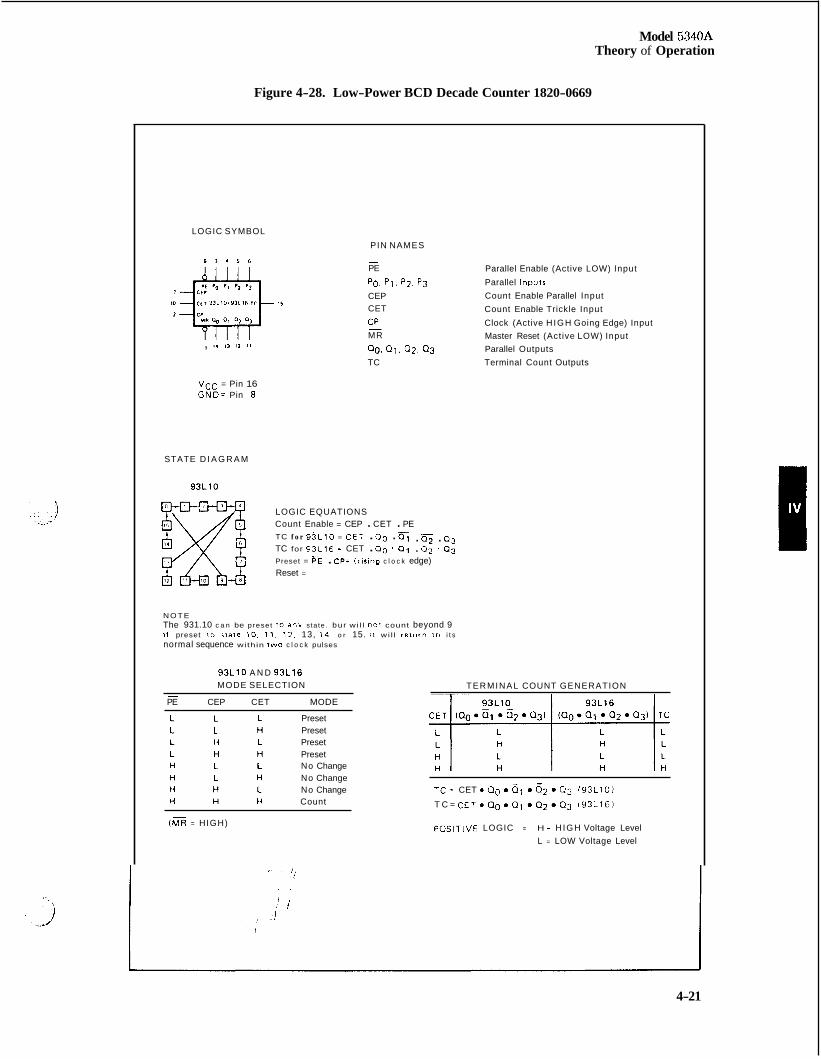
Model 5340A Theory of Operation
Figure 4-28. Low-Power BCD Decade Counter 1820-0669
LOGIC SYMBOL
9 3 4 5 6
, 1. I , 12 I I
PIN NAMES
PE -
Po. p1. p2. p3 CEP CET CP MR
00. 01, Q2. 0 3 TC
-
VCC = Pin 16 GND= Pin 0
STATE D I A G R A M
93L10
LOGIC EQUATIONS Count Enable = CEP . CET . PE TC f o r 9 5 ~ 1 0 = CET . a. . . Cj . 03 TC for 93L16 = CET . Qo ' 0 1 . 02 ' 0 3 Preset =
Reset =
. C P t ( r is ing c l o c k edge)
N O T E The 931.10 c a n be preset to a n y s ta te . bur w i l l not count beyond 9 If preset 10 Irate 10. 11. 12, 13, 14 . o r 15. 11 w i l l r e l o r n 1 0 i t s normal sequence within two c l o c k pulses
93L10 A N D 93L16 MODE SELECTION -
PE CEP CET MODE
Preset Preset Preset Preset No Change No Change No Change Count
(s = HIGH)
Parallel Enable (Active LOW) Input Parallel Inputs Count Enable Parallel Input Count Enable Trickle Input Clock (Active H IGH Going Edge) Input Master Reset (Act ive LOW) Input Parallel Outputs Terminal Count Outputs
TERMINAL COUNT GENERATION
TC = CET 0 00 rn 61 0 6 2 0 0 3 ( 9 3 L l O l
T C = C E T 0 0 0 0 0 1 0 0 2 0 0 3 ( 9 3 L 1 6 )
POSITIVE LOGIC = H = H IGH Voltage Level L = LOW Voltage Level
4-21
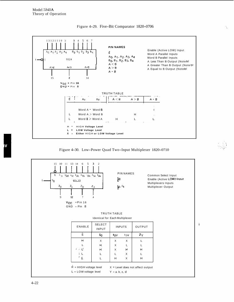
Model 5340A Theory of Operation
ENABLE
Figure 4-29. Five-Bit Comparator 1820-0706
SELECT
INPUT INPUTS OUTPUT
1 3 1 2 1 1 1 0 9 3 4 5 6 7
- E
H
L
' L / * L
'I!
I 9324
SO IOY I1Y ZY
X X X L
H X L L
H X H H
L L X L
L H X H
15 2 14
V c c = P i n 16 G N D = P i n 8
Enable (Active LOW) Input Word A Parallel Inputs Word B Parallel Inputs A Less Than B Output (Note b l A Greater Than B Output (Note b) A Equal t o B Output (Note b)
TRUTH T A B L E
Word A = Word B
L Word A > Word B H
L Word E > Word A H L L
H = H I G H Voltage Level L = L O W Voltage Level X = Either H I G H or L O W Voltage Level
Figure 4-30. Low-Power Quad Two-Input Multiplexer 1820-0710
15 10 1 1 13 14 6 5 3 2
93L22 llsoz; z[ zi I 9 12 7 4
V c c = P i n 1 6
GND = Pin 8
Common Select Input P IN NAMES
SO Enable (Active Low) Input Multiplexers Inputs
10,Il Multiplexer Output z
E
T R U T H TABLE
Identical for Each Multiplexer
= HIGH voltage level X = Level does not affect output
Y = a. b, c . d L = LOW voltage level
i
4-22
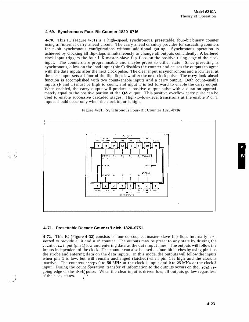
Model 5340A Theory of Operation
4-69. Synchronous Four-Bit Counter 1820-071 6
4-70. This IC (Figure 4-31) is a high-speed, synchronous, presettable, four-bit binary counter using an internal carry ahead circuit. The carry ahead circuitry provides for cascading counters for n-bit synchronous configurations without additional gating. Synchronous operation is achieved by clocking all flip-flops simultaneously to change all outputs coincidently. A buffered clock input triggers the four J-K master-slave flip-flops on the positive rising edge of the clock input. The counters are programmable and maybe preset to either state. Since presetting is synchronous, a low on the load input (pin 9) disables the counter and causes the outputs to agree with the data inputs after the next clock pulse. The clear input is synchronous and a low level at the clear input sets all four of the flip-flops low after the next clock pulse. The carry look-ahead function is accomplished with two count-enable inputs and a carry output. Both count-enable inputs (P and T) must be high to count, and input T is fed forward to enable the carry output. When enabled, the carry output will produce a positive output pulse with a duration approxi- mately equal to the positive portion of the QA output. This positive overflow carry pulse can be used to enable successive cascaded stages. High-to-low-level transitions at the enable P or T inputs should occur only when the clock input is high.
Figure 4-31. Synchronous Four-Bit Counter 1820-0716
O U T P U l Z CARRY ,---< E N A B L t
vcc ouTPu1 oA a0 oc aD T L O A D
CLEAR CLOCU E N A 0 L E G N D U P
D A T A INPUTS
4-71. Presettable Decade Counter/Latch 1820-0751
4-72. This IC (Figure 4-32) consists of four dc-coupled, master-slave flip-flops internally cqn- nected to provide a +2 and a +5 counter. The outputs may be preset to any state by driving the count/load input (pin 1) low and entering data at the data input lines. The outputs will follow the inputs independent of the clock. The counter can also be used as four-bit latches by using pin 1 as the strobe and entering data on the data inputs. In this mode, the outputs will follow the inputs when pin 1 is low, but will remain unchanged (latched) when pin 1 is high and the clock is inactive. The counters aFcept 0 to 50 MHz at the clock 1 input and 0 to 25 MHz at the clock 2 input. During the count operation, transfer of information to the outputs occurs on the negative- going edge of the clock: pulse. When the clear input is driven low, all outputs go low regardless of the clock states. i
I
4-23
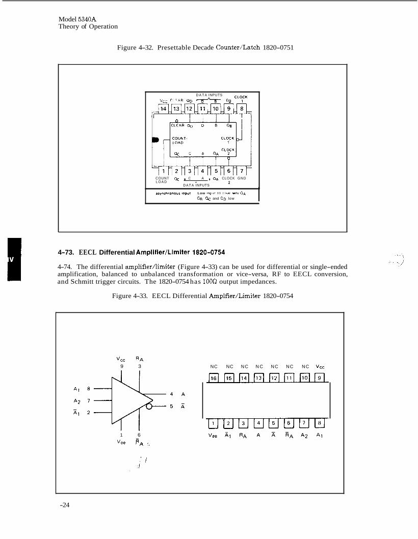
Model 5340A Theory of Operation
Figure 4-32. Presettable Decade Counter/Latch 1820-0751
D A T A INPUTS CLOCK
Vcc C L t A R OD OB 1
COUNT Q , C A , O A CLOCK G N D L O A D 9
D A T A INPUTS 2
asynchronous input Low inpul 10 clear - 1 s O A 0 8 Q and OD low 1
4-73. EECL Differential Amplifier/Limiter 1820-0754
4-74. The differential amplifier/limiter (Figure 4-33) can be used for differential or single-ended amplification, balanced to unbalanced transformation or vice-versa, RF to EECL conversion, and Schmitt trigger circuits. The 1820-0754 has lOOQ output impedances.
Figure 4-33. EECL Differential Amplfier/Limiter 1820-0754
vcc R A 9 3
1 6
Vee F A
NC NC NC N C NC NC NC Vcc
-24
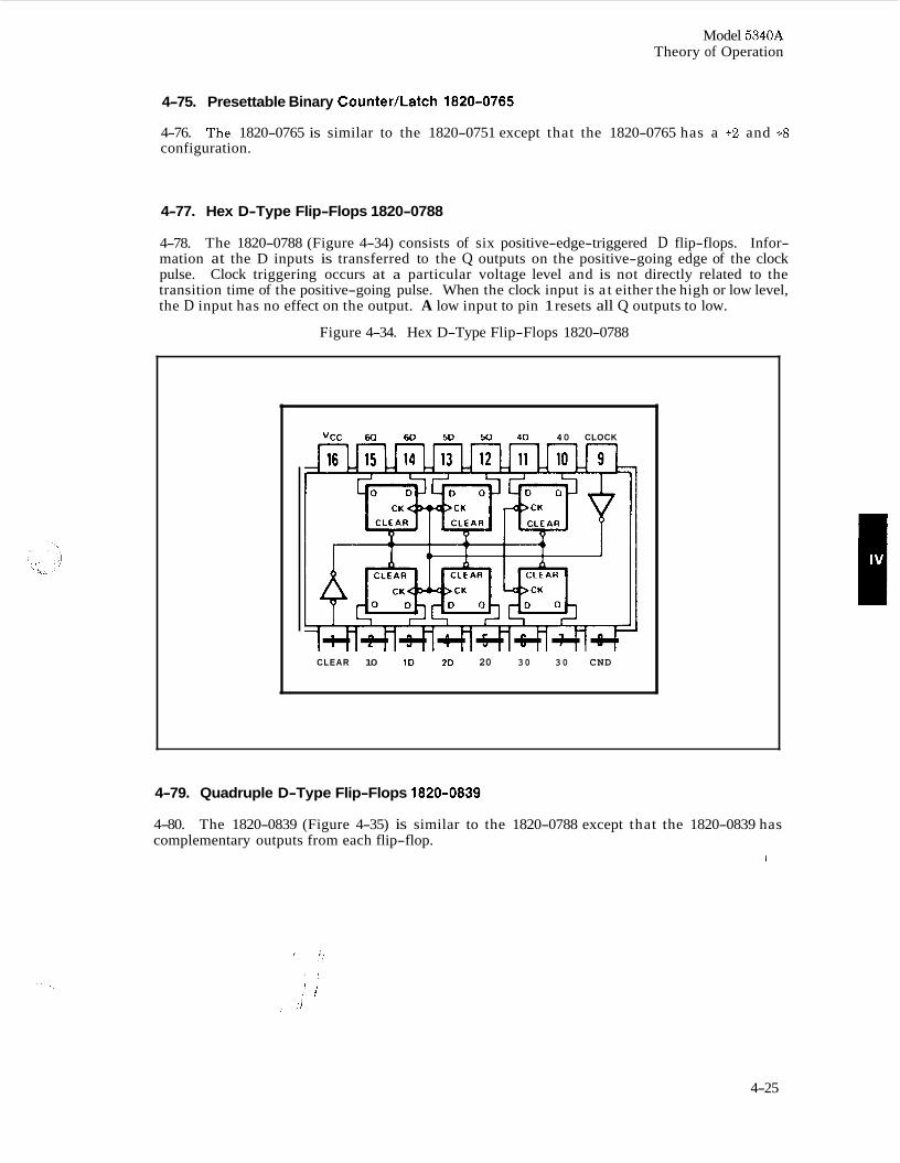
Model 5340A Theory of Operation
4-75. Presettable Binary CountedLatch 1820-0765
4-76. configuration.
"he 1820-0765 is similar to the 1820-0751 except that the 1820-0765 has a +2 and +8
4-77. Hex D-Type Flip-Flops 1820-0788
4-78. The 1820-0788 (Figure 4-34) consists of six positive-edge-triggered D flip-flops. Infor- mation at the D inputs is transferred to the Q outputs on the positive-going edge of the clock pulse. Clock triggering occurs at a particular voltage level and is not directly related to the transition time of the positive-going pulse. When the clock input is a t either the high or low level, the D input has no effect on the output. A low input to pin 1 resets all Q outputs to low.
Figure 4-34. Hex D-Type Flip-Flops 1820-0788
VCC 60 60 5D M 4 0 40 CLOCK
-------- CLEAR 10 1D ZD 20 30 30 CND
4-79. Quadruple D-Type Flip-Flops 1820-0839
4-80. complementary outputs from each flip-flop.
The 1820-0839 (Figure 4-35) is similar to the 1820-0788 except that the 1820-0839 has
I
4-25
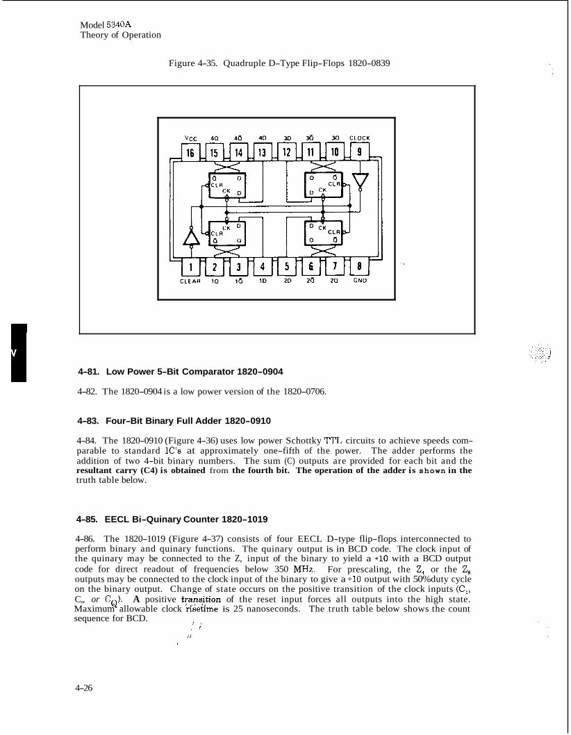
Model 5340A Theory of Operation
Figure 4-35. Quadruple D-Type Flip-Flops 1820-0839
4-81. Low Power 5-Bit Comparator 1820-0904
4-82. The 1820-0904 is a low power version of the 1820-0706.
4-83. Four-Bit Binary Full Adder 1820-0910
4-84. The 1820-0910 (Figure 4-36) uses low power Schottky 'ITL circuits to achieve speeds com- parable to standard IC's at approximately one-fifth of the power. The adder performs the addition of two 4-bit binary numbers. The sum (C) outputs are provided for each bit and the resultant carry (C4) is obtained from the fourth bit. The operation of the adder is shown in the truth table below.
4-85. EECL Bi-Quinary Counter 1820-1019
4-86. The 1820-1019 (Figure 4-37) consists of four EECL D-type flip-flops interconnected to perform binary and quinary functions. The quinary output is in BCD code. The clock input of the quinary may be connected to the Z, input of the binary to yield a el0 with a BCD output code for direct readout of frequencies below 350 MHz. For prescaling, the Z, or the Z, outputs may be connected to the clock input of the binary to give a 110 output with 50% duty cycle on the binary output. Change of state occurs on the positive transition of the clock inputs (C,, C,, or CQ). A positive :ans,i$on of the reset input forces all outputs into the high state. Maximum allowable clock nsetkme is 25 nanoseconds. The truth table below shows the count sequence for BCD.
I , , 4
:i I
4-26
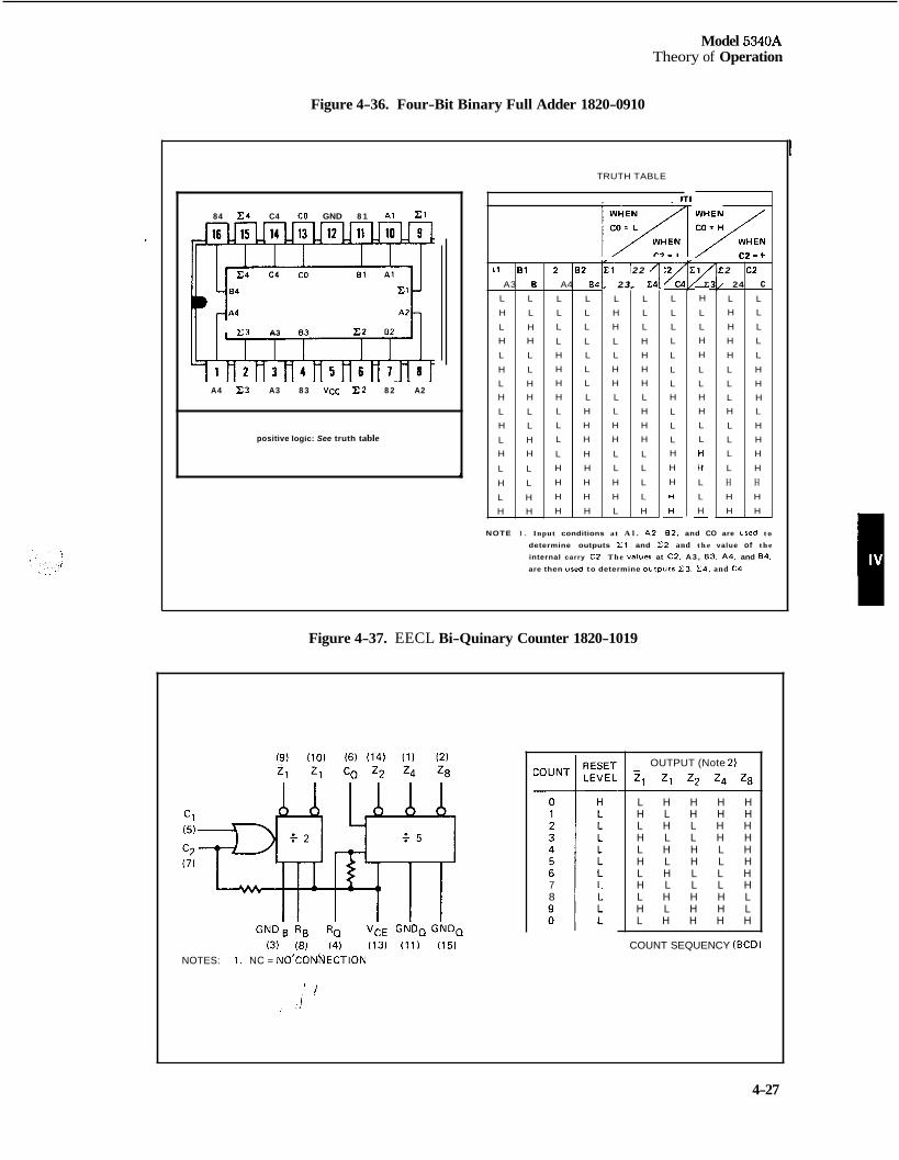
Model 5340A Theory of Operation
positive logic: See truth table
Figure 4-36. Four-Bit Binary Full Adder 1820-0910
k
84 Z 4 C4 CO GND 8 1 A1
C3 A3 8
A4 Z3 A3 8 3 V c c x2 8 2 A2
.2
A4
B2 C1 22
84 2 3 Z L L L L
L L H L
L L H L
L L L H
H L L H
H L H H
H L H H
H L L L
L H L H
L H H H
L H H H
L H L L
H H L L
H H H L
H H H L
H H L H
c2
2
24
L L H L
H L
H L
H L
L H
L H
L H H L
L H
L H
L H
L H
H H H H
H H
TRUTH TABLE
= !-
c2 c
L1
A3
L L
H L
L H H H
L L
H L
L H H H
L L
H L
L H
H H
z L
L
L
L
L
L
L H
L
L
L H
H
H
H H -
B1
B
L L
H L
L H H H
// - z - H
L
L H
H
L
L H
H
L
L H
H
L
L
H - NOTE 1 . Input conditions at A l . A2. 8 2 . and CO are used t o
determine outputs X1 and X 2 and t h e value of t h e
internal carry CZ T h e values at C2. A 3 , 8 3 , A 4 , and 84,
are then used t o determine outputs X 3 , XU, and C4
Figure 4-37. EECL Bi-Quinary Counter 1820-1019
GNDB R B RQ VCE GNDQ GNDQ
(31 (81 (41 (13) (111 (15) NOTES: 1. NC = NO’C~NNECTION
7 8 L
L
OUTPUT (Note 2)
z1 ‘1 ‘2 z4 ‘ 8 -
L H H H H H L H H H L H L H H H L L H H L H H L H H L H L H L H L L H H L L L H L H H H L H L H H L L H H H H
COUNT SEQUENCY (BCD)
4-27
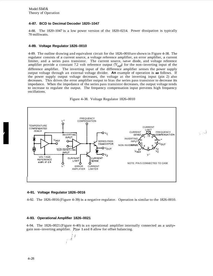
Model 5340A Theory of Operation
4-87. BCD to Decimal Decoder 1820-1047
4-88. 70 milliwatts.
The 1820-1047 is a low power version of the 1820-0214. Power dissipation is typically
4-89. Voltage Regulator 1826-0010
4-89. The outline drawing and equivalent circuit for the 1826-0010 are shown in Figure 4-38. The regulator consists of a current source, a voltage reference amplifier, an error amplifier, a current limiter, and a series pass transistor. The current source, Zener diode, and voltage reference amplifier provide a constant 7.2 volt reference output (Vref) for the non-inverting input of the difference amplifier. The inverting input of the difference amplifier senses the power supply output voltage through an external voltage divider. An example of operation is as follows. If the power supply output voltage decreases, the voltage a t the inverting input (pin 2) also decreases. This drives the error amplifier output to bias the series pass transistor to decrease its impedance. When the impedance of the series pass transistor decreases, the output voltage tends to increase to regulate the output. The frequency compensation input prevents high frequency oscillations.
Figure 4-38. Voltage Regulator 1826-0010
FREQUENCY V + COMPENSATION
TEMPERATURE COMPENSATED
VC
SERIES PASS TRANS ISTO R
NON INVERT1 'OUT
VZ
V - ERROR CURRENT AMPLIFIER LIMITER
CURRENT LIMIT
CURRENT FREQUENCY
INVERTING INPUT
NON INVERTING INPUT u v o ' . 3
VREF VC V -
NOTE: PIN 5 CONNECTED TO CASE
4-91. Voltage Regulator 1826-0016
4-92. The 1826-0016 (Figure 4-39) is a negative regulator. Operation is similar to the 1826-0010.
4-93. Operational Amplifier 1826-0021
4-94. The 1826-0021 (Figure 4-40) is a n operational amplifier internally connected as a unity- gain non-inverting amplifier. Pins 1 and 8 allow for offset balancing.
, , J
j
I ' i I
4-28
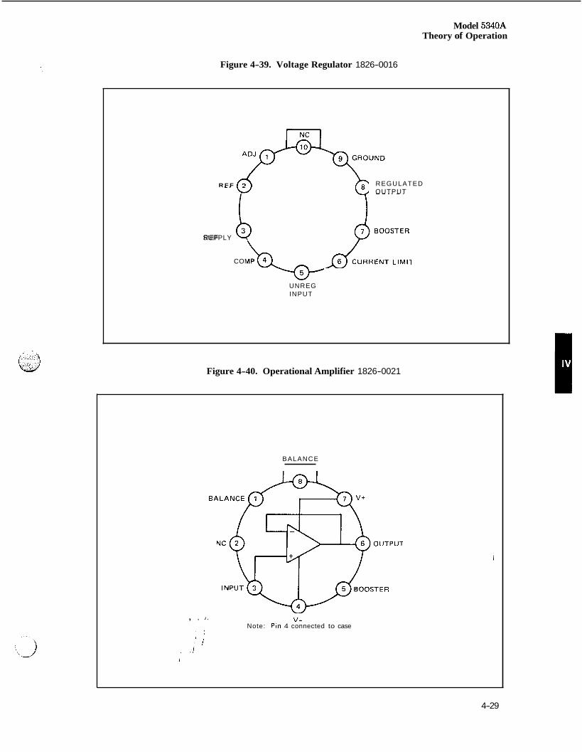
Model 5340A Theory of Operation
Figure 4-39. Voltage Regulator 1826-0016
R F F A
SUPPLY REF b REGULATED
-. w OUTPUT
COMP 4 L UNREG INPUT
Figure 4-40. Operational Amplifier 1826-0021
, , i ,
BALANCE
V- Note: Pin 4 connected to case
4-29
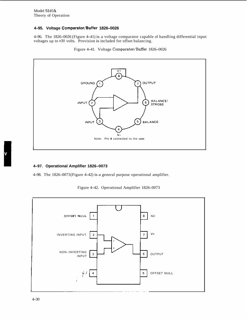
Model 5340A Theory of Operation
4-95. Voltage Comparator/Buffer 1826-0026
4-96. The 1826-0026 (Figure 4-41) is a voltage comparator capable of handling differential input voltages up to *30 volts. Provision is included for offset balancing.
Figure 4-41. Voltage Comparator/Buffer 1826-0026
V- Note: Pin 4 connected t o the case
I
4-97. Operational Amplifier 1826-0073
4-98. The 1826-0073 (Figure 4-42) is a general purpose operational amplifier.
Figure 4-42. Operational Amplifier 1826-0073
INVERTING INPUT
NON- INVERTING INPUT
NC
V +
OUTPUT
OFFSET NULL
4-30
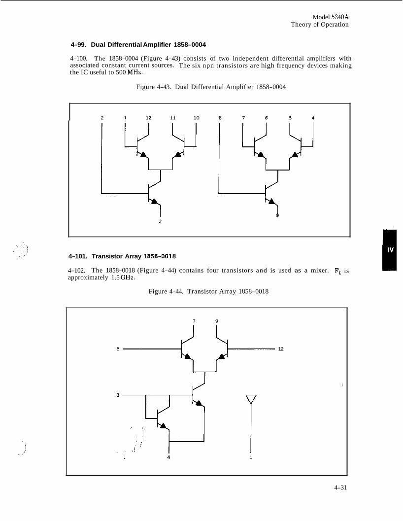
Model 5340A Theory of Operation
. _. 1
4-99. Dual Differential Amplifier 1858-0004
4-100. The 1858-0004 (Figure 4-43) consists of two independent differential amplifiers with associated constant current sources. The six npn transistors are high frequency devices making the IC useful to 500 MHz.
Figure 4-43. Dual Differential Amplifier 1858-0004
2 1 12 1 1 10 8 7 6 5 4
7 9
4-101. Transistor Array 1858-001 8
4-102. approximately 1.5 GHz.
The 1858-0018 (Figure 4-44) contains four transistors and is used as a mixer. Ft is
Figure 4-44. Transistor Array 1858-0018
7 9
12
I 4 1
4-31
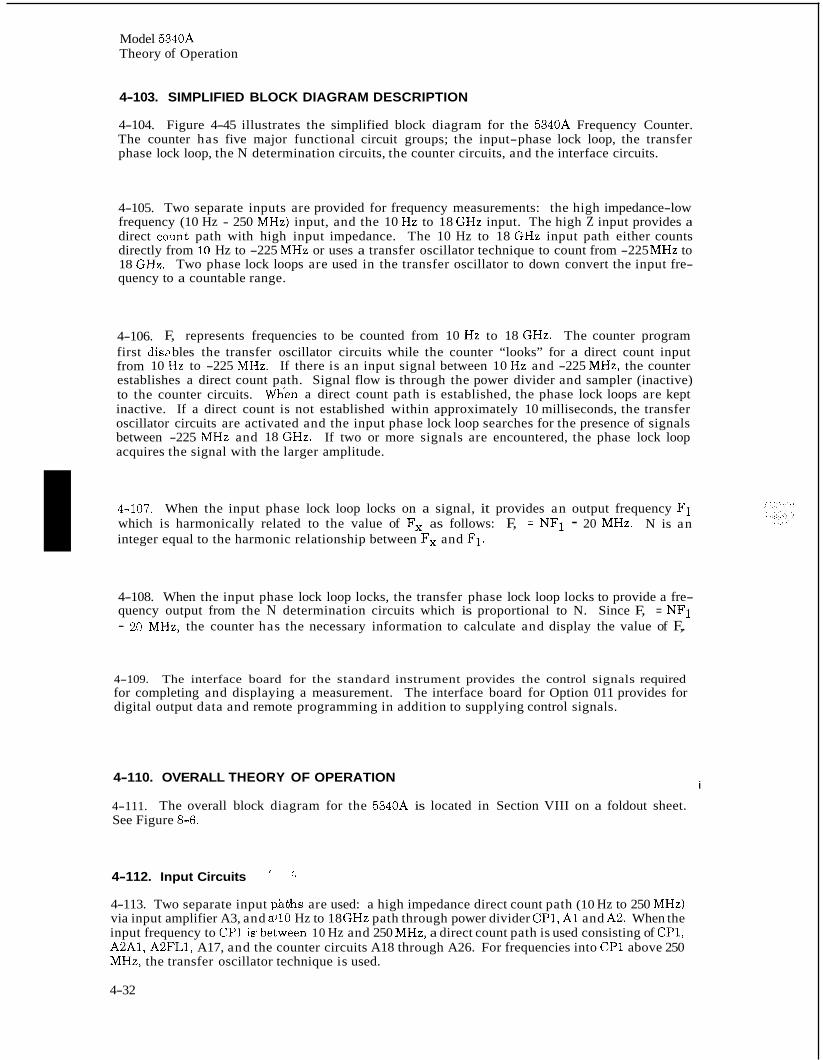
Model 5340A Theory of Operation
4-103. SIMPLIFIED BLOCK DIAGRAM DESCRIPTION
4-104. Figure 4-45 illustrates the simplified block diagram for the 5340A Frequency Counter. The counter has five major functional circuit groups; the input-phase lock loop, the transfer phase lock loop, the N determination circuits, the counter circuits, and the interface circuits.
4-105. Two separate inputs are provided for frequency measurements: the high impedance-low frequency (10 Hz - 250 MHz) input, and the 10 Hz to 18 GHz input. The high Z input provides a direct comt path with high input impedance. The 10 Hz to 18 GHz input path either counts directly from 10 Hz to -225 MHz or uses a transfer oscillator technique to count from -225 MHz to 18 GHz. Two phase lock loops are used in the transfer oscillator to down convert the input fre- quency to a countable range.
4-106. F, represents frequencies to be counted from 10 Hz to 18 GHz. The counter program first disp bles the transfer oscillator circuits while the counter “looks” for a direct count input from 10 Hz to -225 MHz. If there is an input signal between 10 Hz and -225 MHz, the counter establishes a direct count path. Signal flow is through the power divider and sampler (inactive) to the counter circuits. Whkn a direct count path is established, the phase lock loops are kept inactive. If a direct count is not established within approximately 10 milliseconds, the transfer oscillator circuits are activated and the input phase lock loop searches for the presence of signals between -225 MHz and 18 GHz. If two or more signals are encountered, the phase lock loop acquires the signal with the larger amplitude.
4-107. When the input phase lock loop locks on a signal, it provides an output frequency F1 which is harmonically related to the value of F, as follows: N is an integer equal to the harmonic relationship between F, and F1.
F, = NF1 - 20 MHz. I 4-108. When the input phase lock loop locks, the transfer phase lock loop locks to provide a fre- quency output from the N determination circuits which is proportional to N. Since F, = NF1 - 20 MHz, the counter has the necessary information to calculate and display the value of F,.
4-109. The interface board for the standard instrument provides the control signals required for completing and displaying a measurement. The interface board for Option 011 provides for digital output data and remote programming in addition to supplying control signals.
i 4-110. OVERALL THEORY OF OPERATION
4-111. See Figure 8-6.
The overall block diagram for the 5340A is located in Section VIII on a foldout sheet.
4-112. Input Circuits ‘ ‘,
4-113. Two separate input pabhs are used: a high impedance direct count path (10 Hz to 250 MHz) via input amplifier A3, and d l 0 Hz to 18 GHz path through power divider CP1, A1 and A2. When the input frequency to CPl is’between 10 Hz and 250 MHz, a direct count path is used consisting of CP1, A2A1, A2FL1, A17, and the counter circuits A18 through A26. For frequencies into CP1 above 250 MHz, the transfer oscillator technique is used.
4-32
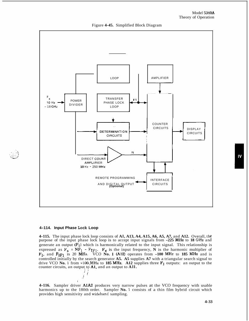
Model 5340A Theory of Operation
Figure 4-45. Simplified Block Diagram
LOOP AMPLIFIER
D ETERM I N AT1 O N
b
TRANSFER ~1 POWER
F X
D ETERM I N AT1 O N
PHASE LOCK LOOP
DIV IDER 1 0 H z +
- 18 GHz A
COUNTER CIRCUITS
4 2 +
DIRECT COUNT AMPLl F I ER
10 H Z - 250 MHz
DISPLAY CIRCUITS
INTERFACE REMOTE PROGRAMMING
(Optional) A N D D I G I T A L OUTPUT CIRCUITS I
4-114. Input Phase Lock Loop
4-115. The input phase lock loop consists of Al, A13, A4, A15, A6, A5, A7, and A12. Overall, th
generate an output (F1) which is harmonically related to the input signal. This relationship is expressed as Fx = NF1 - F I F ~ . F, is the input frequency, N is the harmonic multiplier of F1, and F I F ~ is 20 MHz. VCO No. 1 (A12) operates from -100 MHz to 185 MHz and is controlled initially by the search generator A5. A5 supplies A7 with a triangular search signal to drive VCO No. 1 from 7100,:MHz to 185 MHz. A12 supplies three F1 outputs: an output to the counter circuits, an output to Al , and an output to A l l .
I 1
purpose of the input phase lock loop is to accept input signals from -225 MHz to 18 GHz an !
<I i .i
I 4-116. harmonics up to the 180th order. provides high sensitivity and wideband sampling.
Sampler driver A1A2 produces very narrow pulses at the VCO frequency with usable Sampler No. 1 consists of a thin film hybrid circuit which
4-33
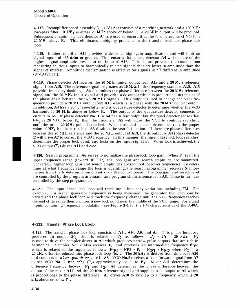
Model 5340A Theory of Operation
4-117. Preamplifier board assembly No. 1 (AlA4) consists of a matching network and a 100 MHz low-pass filter. If NF1 is either 20 MHz above or below F,, a 20 MHz output will be produced. Subsequent circuits in phase detector A4 are used to ensure that the Nth harmonic of VCOl is 20 MHz above F,. This eliminates ambiguity problems in the transfer oscillator phase lock loop.
4-1 18. Limiter amplifier A13 provides wide-band, high-gain amplification and will limit on signal inputs of -35 dBm or greater. This ensures that phase detector A4 will operate on the highest signal amplitude present at the input of A13. This feature prevents the counter from measuring spurious inputs or harmonically related signals that are lower in amplitude than the signal of interest. Amplitude discrimination is effective for signals 20 dB different in amplitude (10 dB typical).
4-119. Phase detector A4 receives the 20 MHz limiter output from A13 and a 20 MHz reference signal from A15. The reference signal originates as 10 MHz in the frequency standard A18. A15 provides frequency doubling. A4 determines the phase difference between the 20 MHz reference signal and the 20 MHz input signal and provides a dc output which is proportional to the sine of the phase angle between the two 20 MHz signals. This output is used to change the VCO fre- quency to provide a 20 MHz output from A13 which is in phase with the 20 MHz doubler output. In addition, A4 has a 90" phase-shifter and a quadrature detector to determine whether the VCO harmonic is 20 MHz above or below F,. The output of the quadrature detector connects to circuits in A5. If phase detector No. 1 in A4 has a zero output but the quad detector senses that NF1 is 20 MHz below F,, then the circuits in A5 will allow the VCO to continue searching until the other 20 MHz point is reached. When the quad detector determines that the proper value of NF1 has been reached, A5 disables the search function. If there are phase differences between the 20 MHz reference and the 20 MHz output of A13, the dc output of A4 (phase detector 1) will drive A7 to correct the VCO frequency. In this manner, the input phase lock loop searches, determines the proper lock point, and locks on the input signal F,. When lock is achieved, the VCO output (F1) drives A l l and A22.
4-120. Search programmer A6 serves to normalize the phase lock loop gain. When F, is in the upper frequency range (toward 18 GHz), the loop gain and search amplitude are minimized. Conversely, higher loop gain and search amplitudes are required for lower frequencies. To deter- mine at what frequency range the loop is operating, the search programmer receives N infor- mation from the N determination circuitry via the control board. The loop gain and serach level are controlled by the program attenuator and program shunt attenuator in A6. These in turn are controlled by the step programmer.
4-121. For example, if a signal generator frequency is being measured, the generator frequency can be varied and the phase lock loop will track the frequency change until the VCO frequency reaches the end of its range then acquires a new lock point near the middle of the VCO range. For signal inputs containing frequency modulation, see Figure 3-1 for the FM characteristics of the 5340A.
I The input phase lock loop will track input frequency variations including FM.
4-122. Transfer Phase Lock Loop
4-123. The transfer phase lock loop consists of A l l , A10, A9, and A8. This phase lock loop produces an output (F2) that is related to F1 as follows: F2 = F1 f 20 kHz. F2 is used to drive the sampler driver in A2 which produces narrow pulse outputs that are rich in harmonics. Sampler No. 2 also receives F, and produces a n intermediate frequency F I F ~ which is related to the inputs as follows: F I F ~ = NF2 - F, = F I F ~ f NFO; where F o is a 20 kHz offset introduced into phase lock loop No. 2. The 20 kHz is derived from time base A20 and connects to a bandpass ,filter gate in A8. VCO No.2 receives a feed-forward signal from A7 to set VCO No. 2 frequencp (F2) approximately equal to F1. Mixer A l l determines the difference frequency betwekn F1 and F2. A8 determines the phase difference between the output of the mixer A l l land the 20 kHz reference signal and supplies a dc output to A9 which is proportional to the phase difference. A9 drives A10 to lock F2 to a frequency which is 20 kHz above or below F1.
4-34
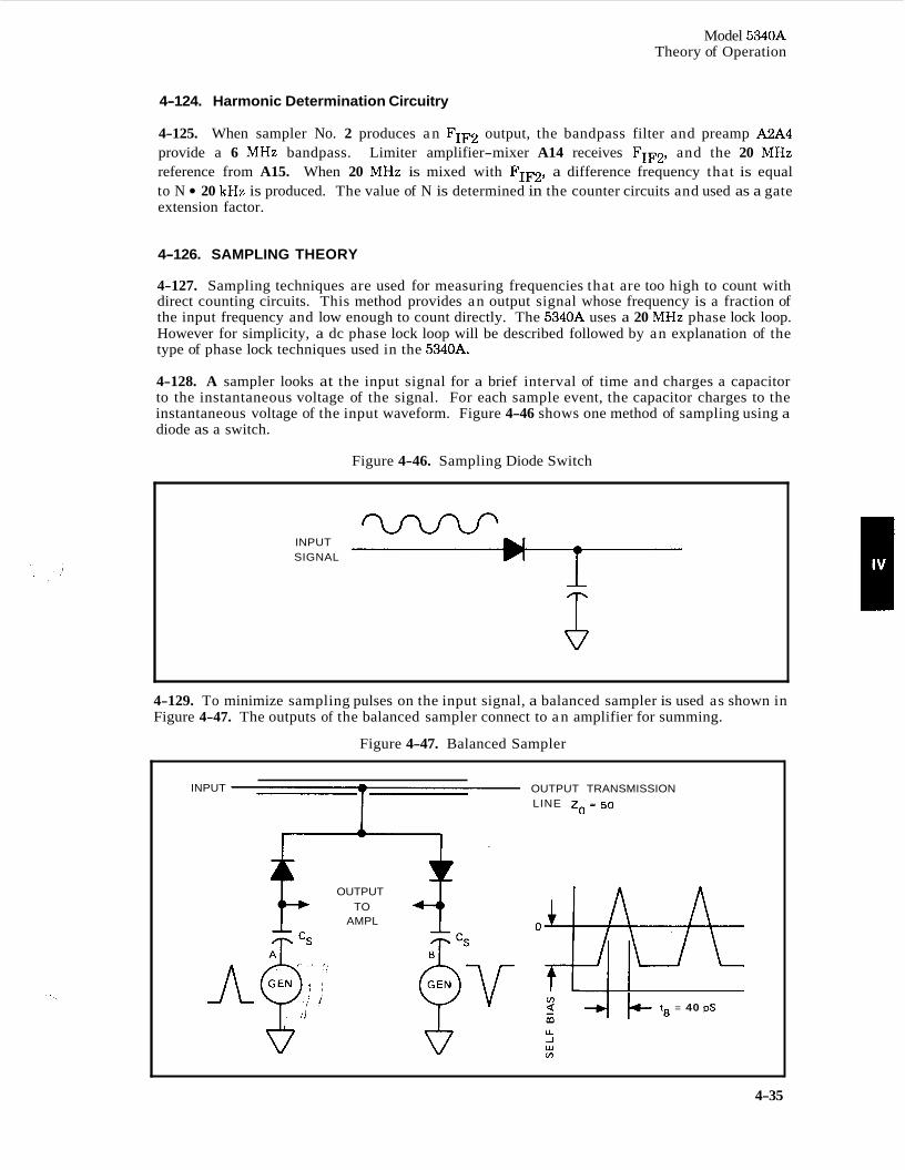
Model 5340A Theory of Operation
4-124. Harmonic Determination Circuitry
4-125. When sampler No. 2 produces a n F I F ~ output, the bandpass filter and preamp A2A4 provide a 6 MHz bandpass. Limiter amplifier-mixer A14 receives FIF2, and the 20 MHz reference from A15. When 20 MHz is mixed with FIF2, a difference frequency that is equal to N 20 kHz is produced. The value of N is determined in the counter circuits and used as a gate extension factor.
4-126. SAMPLING THEORY
4-127. Sampling techniques are used for measuring frequencies that are too high to count with direct counting circuits. This method provides an output signal whose frequency is a fraction of the input frequency and low enough to count directly. The 534QA uses a 20 MHz phase lock loop. However for simplicity, a dc phase lock loop will be described followed by an explanation of the type of phase lock techniques used in the 5340A.
4-128. A sampler looks at the input signal for a brief interval of time and charges a capacitor to the instantaneous voltage of the signal. For each sample event, the capacitor charges to the instantaneous voltage of the input waveform. Figure 4-46 shows one method of sampling using a diode as a switch.
Figure 4-46. Sampling Diode Switch
==+- INPUT SIGNAL
4-129. To minimize sampling pulses on the input signal, a balanced sampler is used as shown in Figure 4-47. The outputs of the balanced sampler connect to a n amplifier for summing.
Figure 4-47. Balanced Sampler
OUTPUT TRANSMISSION LINE z o = 50
INPUT
OUTPUT TO
AMPL
v
* +t
t7 t8 = 40 pS I+
4-35
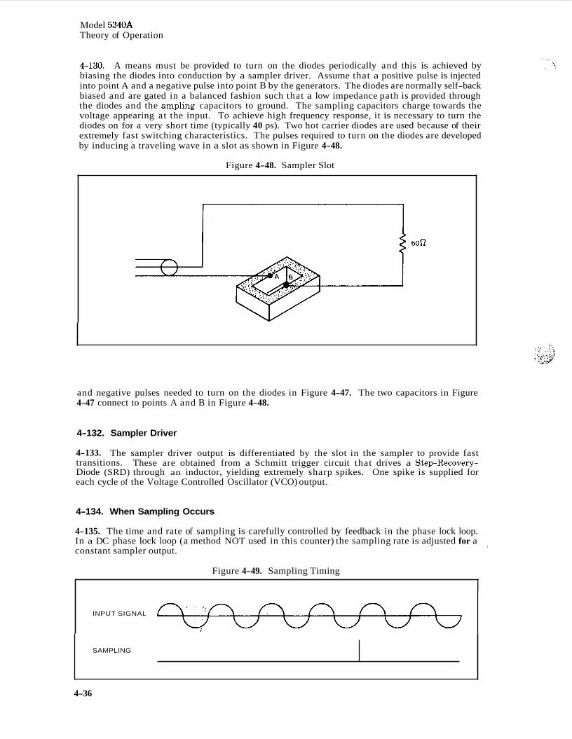
Model 5340A Theory of Operation
SAMPLING
4-130. A means must be provided to turn on the diodes periodically and this is achieved by biasing the diodes into conduction by a sampler driver. Assume that a positive pulse is injected into point A and a negative pulse into point B by the generators. The diodes are normally self-back biased and are gated in a balanced fashion such that a low impedance path is provided through the diodes and the ampling capacitors to ground. The sampling capacitors charge towards the voltage appearing at the input. To achieve high frequency response, it is necessary to turn the diodes on for a very short time (typically 40 ps). Two hot carrier diodes are used because of their extremely fast switching characteristics. The pulses required to turn on the diodes are developed by inducing a traveling wave in a slot as shown in Figure 4-48.
Figure 4-48. Sampler Slot
and negative pulses needed to turn on the diodes in Figure 4-47. The two capacitors in Figure 4-47 connect to points A and B in Figure 4-48.
4-132. Sampler Driver
4-133. transitions. Diode (SRD) through an inductor, yielding extremely sharp spikes. each cycle of the Voltage Controlled Oscillator (VCO) output.
The sampler driver output is differentiated by the slot in the sampler to provide fast These are obtained from a Schmitt trigger circuit that drives a Step-Recovery-
One spike is supplied for
4-134. When Sampling Occurs
4-135. The time and rate of sampling is carefully controlled by feedback in the phase lock loop. In a DC phase lock loop (a method NOT used in this counter) the sampling rate is adjusted for a constant sampler output.
,
Figure 4-49. Sampling Timing
1 INPUT SIGNAL
4-36
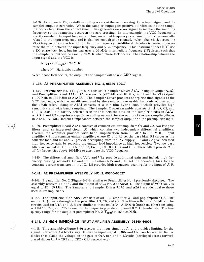
Model 5340A Theory of Operation
4-136. As shown in Figure 4-49, sampling occurs at the zero crossing of the input signal, and the sampler output is zero volts. When the sampler output goes positive, it indicates that the sampl- ing occurs later than the correct time. This generates an error signal to increase the sampling frequency so that sampling occurs at the zero crossing. In this example, the VCO frequency is exactly one-half the input frequency. Thus, an output frequency is obtained that is harmonically related to the input frequency and is also low enough to be counted. When phase lock occurs, the VCO frequency is some fraction of the input frequency. Additional circuitry is needed to deter- mine the ratio between the input frequency and VCO frequency. This instrument does NOT use a DC phase-lock loop, but instead uses a 20 MHz intermediate frequency (IF) circuit such that the sampler output will be exactly 20 MHz when phase lock occurs. The relationship between the input signal and the VCO is:
where N = Harmonic number
When phase lock occurs, the output of the sampler will be a 20 MHz signal.
4-137. A1 PREAMPLIFIER ASSEMBLY NO. 1, 05340-60017
4-138. Preamplifiek No. 1 (Figure 8-7) consists of Sampler Driver AlA2, Sampler Output AlA3, and Preamplifier Board AlA4. A1 receives Fx (-225 MHz to 18 GHz) at 52 and the VCO signal (-100 MHz to 185 MHz) at AlA2Jl. The Sampler Driver produces sharp rise time signals at the VCO frequency, which when differentiated by the sampler have usable harmonic outputs up to the 180th order. Sampler AlAl consists of a thin-film hybrid circuit which provides high sensitivity and wide band sampling. The Sampler Output assembly consists of R1, C1, C2, and Ll. AlA3R1 is a factory selected resistor that sets the bias on the sampler diodes in AlA1. AlA3Cl and C2 comprise a capacitive adding network for the output of the two sampling diodes in AlAl. AlA3Ll matches impedances between the sampler output and the preamplifier input.
4-139. Preamplifier Board A1A4 consists of common emitter amplifiers Q1 and Q2, two low pass filters, and an integrated circuit U1 which contains two independent differential amplifiers. Overall, the amplifier provides wide band amplification from .1 MHz to 100 MHz. Input amplifier Q1 is a common emitter amplfier; where R1 and R2 set the base bias, R4 serves as the collector load and R3 and C1 provide decoupling from the +5V supply. R6 and C2 give increased high frequency gain by reducing the emitter load impedance at high frequencies. Two low pass filters are included: L1, C3-C5, and L3, L4, L6, C9, C11, C13, and C15. These filters provide roll- off for frequencies above 100 MHz to attenuate the VCO frequency.
4-140. The differential amplifiers U1A and U1B provide additional gain and include high fre- quency peaking networks L7 and L9. Resistors R15 and R16 set the operating bias for the constant-current transistor in the IC. L8 provides high frequency peaking for the input of UlB.
4-141. A2 PREAMPLIFIER ASSEMBLY NO. 2, 05340-60027
4-142. Preamplifier No. 2 (Figure 8-8) is similar to Preamplifier No. 1 previously discussed. The assembly receives Fx at 52 and the output of VCO No. 2 at A2A2J1. The output of VCO No. 2 is equal to F1 *20 kHz. The Sampler and Sampler Driver A2A1 and A2A2 are identical to those used in Preamplifier Al.
\
4-143. The input circuit on A2A4 consists of a n FET amplifier Q1 and pnp amplifier Q2. The output of Q2 feeds through a low pass filter L3, C6, and C7. The filter rolls off at 60 MHz. The circuits used for U1A and U1B are similar to those on AlA4. A 20 MHz bandpass filter consisting of L8-Ll0, C20, and C22 is used in the output to provide an overall 8 MHz bandwidth. The fre- quency range for the output of preamplifier No. 2 (FIF~) is 16 to 24 MHz.
4-144. A3 HIGH-IMPEDAPCE INPUT AMPLIFIER ASSEMBLY, 05340-60001
4-145. This assembly, (Figure 8-9) receives the input signal at 54 and provides limiting for the signal. Capacitor C4 blocks any DC on the input signal. CR5 and CR6 are hot-carrier limiter diodes that clamp the voltage on the gate of Q1A to + and - 1.3 volts (developed across forward biased diodes CR1 - CR3 and CR2 - CR4 respectively).
4-37
I ,
.i
Model 5340A Theory of Operation
4-146. Q1B is a current source for Q1A to maintain the proper DC level for the input to U1. Varying R10 changes the DC level on the drain of Q1B. Q1A is a unity gain amplifier that presents a high input impedance to 54. To compensate for the loss of Q1A transconductance at high frequencies and to keep the gain constant, C6 and R6 shunt high frequencies past QlA.
4-147. U1 is used as an RF to EECL converter. A reference voltage is maintained on U1 pin 8 and the RF input signal is applied to pin 2. When pin 2 is more positive than pin 8, the output on pin 4 will be logic high (EECL logic levels). A complementary output on U1 pin 5 is detected by CR9 - C15 and CRlO 4 1 6 to give automatic base line shift to compensate for the shift due to a non- symmetrical input signal (such as a pulse train). When the output goes negative for more than a 50% duty cycle, Q2 will turn on, forming a divider network of R17 and R12 with the +15V supply. This raises the reference voltage at Ul(8) by half the hysteresis of the circuit to increase the sensitivity to a positive pulse train.
4-148. When Option 002 is installed, a rear panel connector 58 is installed in parallel with 54. To ensure that the instrument meets all specifications, a 50-ohm termination (R4) is normally installed on the front panel connector 54. R4 should be connected to the rear panel connector 58 when it is desired to use the front panel input.
4-149. A4 PHASE DETECTOWQUAD DETECTOR ASSEMBLY, 05340-60002
4-150. The Phase Detector (Figure 8-10) consists of 20 MHz bandpass filter L1, L2, C5, C7, and R14; 90" phase shifter Q3, L4, and C13; quad detector CR6-CR9; phase detector CR1-CR4; and detector drivers Q1 and Q2. The detector receives the 20 MHz IF at pin 12 from Limiter/ Amplifier A13 and the 20 MHz reference signal at pin 15 from the 10 MHz Doubler. Overall, the circuits detect the phase difference between the two inputs and determine whether the VCO harmonic is 20 MHz above or below Fx.
4-151. The 20 MHz signal from A13 goes through the bandpass filter to the phase detector and to the 90" phase shifter. The filter is tuned to 20 MHz with a bandpass of 7 MHz. The 20 MHz refer- ence signal is routed to a differential amplifier Q4-Q5. Q6 is a constant current source for the I differential amplifier.
1
4-152. Phase detector No. 1 compares the phase of the 20 MHz reference to the phase of the 20 MHz IF. When phase differences exists, the phase detector produces a dc output which is used to drive the VCO to produce an output which is phase coherent with the 20 MHz reference signal. When phase coherence is achieved, the quad detector detects whether the VCO harmonic is 20 MHz above or below Fx. When the VCO harmonic is 20 MHz above Fx, the quad detector output is about -450 mV; and slightly positive when the VCO harmonic is 20 MHz below Fx. The -450 mV output is used to lock the loop.
4-153. Q4 and Q5 produce two reference signals of opposite phase to drive the phase detector and the quad detector. The reference signal is coupled through C8 and C10 to the phase detector. C14 and C16 provide coupling for the reference signal to the quad detector. The phase detectors produce a n output which is proportional to the sine of the phase difference between the two inputs. For example, when the two inputs are exactly in phase, the output of the phase detector is zero. At 90" phase difference, the output is maximum. The detector drivers Q1 and Q2 provide the required filtering and level shifting for the phase detector outputs. The 90" phase shifter Q3 uses an LC network to shift the phase of the 20 MHz IF to be in quadrature (90") with the reference signal.
4-154. A5 SEARCH ASSEMBLY, 05340-60003 I i i
4-155. The Search Assembly (Figure 8-11) consists of Schmitt triggers U2 and U4, buffers Q2 and Q3 and operational amplqers U1 and U3 which serve as a ramp integrator. The circuits receive two inputs, one from,,Quad Detector A4 and the other from Search Programmer A6. The quad detector output determines if the lock is valid. When the quad detector on A4 detects that the VCO harmonic is 20 MHz above Fx, the quad detector supplies a negative signal to A5(8).
4-38
Model 5340A Theory of Operation
A negative level a t pin 8 turns U2 and U4 off which turns off Q1. Q1 determines when the search ramp signal is routed to DC Compensation Amplifier A7. The search ramp signal is derived from the search pulse signal which is supplied from Search Programmer A6. U1 and U3 function as an integrator to provide a ramp voltage output. C7 is the integrating capacitor and R15 sets the dc level for the ramp signal.
4-156. A6 SEARCH PROGRAMMER ASSEMBLY, 05340-60004
4-157. The Search Programmer (Figure 8-12) determines the search ramp amplitude and sets the loop gain compensation. The circuits consist of counter U4, binary to decimal decoder U2, buffer U1, loop compensation switches Q1 through Q6, search programming switches Q7 through Q12, and pulse conditioner U5.
4-158. Pulse conditioner U5 is a one-shot multivibrator used to shape the incoming start search pulse from A21. C1 and R3 set the multivibrator pulse width at 5 milliseconds. The prf is deter- mined by Control Assembly A21. The conditioned pulse is used by the Search Assembly A5 to derive the search ramp signal.
4-159. The counter circuit U4 receives three-line binary data and a strobe from interface assembly A19. In addition, U4 receives the inhibit control and start search signals from A21. These are used to drive the clock 2 input and the reset input of U4. The strobe input allows parallel-entry for the DB, DC, and DD inputs. When the strobe line receives a logic 0, the data inputs are transferred to the D, C, and B outputs (U4 pins 12, 2, and 9). Counting occurs on the negative going edge of the input clock pulse. The count function will start from the number strobed in or will start from zero when the counter is reset. The outputs are binary and connect to a binary-to-decimal decoder U2. U2 provides a decimal output between 0 and 6. As an example of operation, assume that U2 receives A=H, B=H, and C=L. With this input, the 3 line (pin 4) goes low to drive Ul(4) high. With Ul(4) high, Q4 and QlO are on and all other FET’s are off. For this programming segment, R11, C8, and R19 provide the proper loop compensation and R25 sets the search amplitude. Two modes of operation can be selected, normal and programmed.
4-160. A7 DC AMPLIFIER/COMPENSATOR NO. 1 ASSEMBLY, 05340-60005
4-161. A7 (Figure 8-13) consists of lock mode switches Ql, Q2, Q3, Q6, and dc amplifiers U1 and Q4, Q5, QS, Q9. The lock mode switches are controlled by the search switch signal from A5 and the input loop lock from A5. The output from Phase Detector No. 1 represents the error signal required to drive VCO No. 1 to be phase coherent with the 20 MHz reference signal. When Q2 is on, the phase detector signal is amplified by U1. R13 sets the dc level output. R27 sets the gain of Q4 and QS. Diodes CR5 and CR8 provide limits for the maximum dc.
4-162. A8 BANDPASS FILTEWPHASE DETECTOR ASSEMBLY, 05340-60006
4-163. The BPF/Phase Detector Assembly (Figure 8-14) consists of a bandpass filter amplifier U1, comparator U2, retriggerable one-shot multivibrator U3B, sampler driver U3A, sampler Q2, and high impedance amplifiers Q1A and Q1B. A8 receives the 20 kHz reference signal from Time Base A20 and the 20 kHz mixer signal from Mixer A l l . A8 produces two outputs: the trans- fer loop SEARCH signal and the phase detector 2 signal. The transfer loop SEARCH signal is sent to DC Compensator Amplifier A9. A9 uses the transfer loop SEARCH signal as an indi- cation of loop lock. The phase detector 2 output is used to drive VCO 2 so that the 20 kHz mixer signal is coherent with the 20 kHz reference signal.
4-164. The input to’Ul‘,is the mixer output from A l l at approximately 1V peak-to-peak amplitude. U1 is an operational amplifier connected in a bandpass filter feedback configuration. The filter is tuned to 20 kgz with a Q of about 2 and a bandpass of *5 kHz at the 3 dB points.
4-165. Comparator u 2 compares the output level of U1 with the positive level set by R13. When the output level of U1 exceeds the level set by R13, U2 produces a positive output to trigger U3B. U3B is a retriggerable one-shot multivibrator. When U3B pin 12 goes high, the multivibrator triggers to drive U3B pin 10 high for approximately 50 psec. The duration of the 50 psec
, :i
4-39
Model 5340A Theory of Operation
pulse is determined by R20 and C19. The multivibrator can be retriggered at any time during the 50 psec period to establish a new 50 psec pulse output. As long as the multivibrator is retrig- gered within 50 psec, the Q output U3(10) will remain high. In practice, this is the manner in which the circuit operates. Since U2 turns on and off for each cycle of its input, U3B will be retriggered as long as the signal at UZ(2) is sufficient to trigger comparator U2. When lock is achieved, U3B(10) is high.
4-166. In the phase detector portion of A8, C16 couples the 20 kHz mixer signal through a high impedance tie point to Q2. The high impedance tie point prevents humidity from discharging the high impedance points and C18. Q2 is a n N-channel insulated gate field-effect transistor (IGFET) used as a sampler, U3A generates 0.8 psec (*0.2 psec) pulses to gate Q2 on and off at the 20 kHz reference rate. The mixer signal from A l l is sampled by QZ to produce a charge across C18. When the mixer signal is at 20 kHz and is coherent with the 20 kHz reference signal, the voltage across c18 will be dc. When the loop is out of lock, the voltage across C18 is ac. The frequency of this ac is the difference between the instantaneous values of the reference signal and the mixer signal. U3A is disabled when U3B(10) is low, thereby preventing sampler operation until the transfer loop SEARCH line goes high. This prevents false locks on har- monics of 20 kHz such as 10 kHz, 40 kHz, etc.
4-167. Q1A and Q1B comprise a dc stabilized FET pair. Connecting Q1A and Q1B between + and - 15 volts reduces the dc variation on the output of pin 6. CR2 and CR3 provide *lo volts for proper operation of Q1A and Q1B. C20 through C23 filter out noise generated in the Zener diodes. 4-168. When phase lock is achieved, the dc output of Q1A and Q1B is amplified by DC Com- pensator/Amplifier No. 2 A9. A9 drives the VCO 2 (A10) frequency to maintain a 20 kHz differ- ence frequency out of A l l which is phase coherent with the 20 kHz reference signal.
4-169. A9 DC AMPLlFIER/COMPENSATOR NO. 2 ASSEMBLY, 05340-60007
4-170. This assembly (Figure 8-15) performs two main functions. One of the functions provides dc amplification and compensation required for the loop gain and frequency response charac- teristics. The other function is to process the search and lock signals to develop a transfer loop lock output to “tell” the counter circuits when the transfer loop is locked.
I 4-171. U1 is a low-noise operational amplifier which provides dc gain combined with a lag net- work. The dc gain is variable from approximately 1 to 25 as determined by the ratio of R8 to R4 + R2. R1 inserts a current into the operational amplifier input to adjust the dc offset. The lag network consists of C5, C7, R11, and R8. At higher frequencies, C5 and C7 increase the amount of feedback to reduce the gain. Figure 4-50 shows the frequency response of amplifier U1. The rolloff characteristics are designed to provide the proper compensation for the loop.
Figure 4-50. Frequency Response of A9 Input Amplifier
GAIN
, , I !
’ 1 :.I
i FREQ
4-40
Model 5340A Theory of Operation
4-172. U2 serves a s a summing amplifier for the phase detector output and the output of U4. The gain of U2 for the phase detector signal is 5 as set by R20 and R15. The gain for the output of U4 is 1 as determined by R20 and R13. The output of U2 is between 75 and +13 volts and is used to fine tune VCO 2.
4-173. The search signal is a sawtooth waveform which is developed across C8. When the level at A9(8) is low, Q1 is off and Q3 is on. This allows C8 to charge through Q3 and R12 toward +15 volts. The high-impedance tie point is a teflon-insulated connector that prevents humidity from discharging C8. The ramp developed on C8 couples through a voltage follower U4 to comparator U3. U3 has a +5V reference input at pin 2. After 30 milliseconds, the ramp voltage at U4(6) will reach +5 volts and U3(7) will trigger one-shot multivibrator U6A for 2.5 milliseconds. When U6A(6) goes high, Q2 turns on to discharge C8. This develops the flyback portion of the sawtooth, which lasts for 2.5 milliseconds. U6A can also be triggered when the input loop lock signal at A9(12) goes high. C4 and L4 differentiate this input into a spike which triggers U6A to discharge C8 and start the transfer loop search cycle. When a harmonic of the VCO frequency beats against the incoming Fx to produce a n approximate 20 kHz difference, the transfer loop SEARCH signal goes high. When A9(8) is high, Q1 switches on to turn off Q3. This interrupts the charging source for C8 allowing C8 to maintain its charge.
4-174. The transfer loop LOCK signal is developed by ANDing the transfer loop SEARCH signal an the input loop lock signal. As an example of operation, assume that the input loop is locked (A9 pin 12 is high) but the transfer loop search signal at A9 pin 8 is low. Under these conditions, U5C pins 9 and 10 are high but U5C pin 11 is low. Thus there is no transfer loop LOCK signal at A9(7), i.e., A9(7) is high. When A9(8) goes high, U5C(ll) will go high after 100 nsec and U5C(10) will go high after 10 msec. U5A and B provide the 100 nsec delay and U6B gives the 10 msec delay. The purpose of U5B and A is to prevent U5C(8) from going low at the first instant that A9(12) and A9(8) are both high. This allows U6B to provide an overall delay of 10 msec before U5C(8) can go low. Thus the circuit “waits” for 10 msec to ensure a stable lock. The closed loop bandwidth of the transfer phase lock loop is 5 kHz. Figure 4-51 shows the timing relationship of the circuits.
Figure 4-51. Transfer Loop Timing Diagram
INPUT LOOP I LOCK
FLYBACK
LOSE LOCK NO LOCK
RELOCK
RAMP SEARCH TP3 ?&&pr I I I I I I I I I
3 6 m r LJ I I 1 1 I 1 I I I
2 5 m r - W I I
I 1 1 I I 1 I 1 I I 1 1 I 1 1 I I I I I
TP2 2 5 ms I I I I I I I I I I I I I I
10 rns I I
I
SEARCH A9181 I I I I J TRANSFER LOOP I I I
I
I I I
I I
U5C(101 I
I I
’ < I , I
U 5 C ( l l l I
4 J I
I I I I I 1l-T I I
‘ I
I I
I I I I I
I I I I I
I I I
I ! 1
100 ntec + f
/
TRANSFER LOOP 1 LOCK A9(7l I -
I
4-41
Model 5340A Theory of Operation
4-175. A10 VCO NO. 2 ASSEMBLY, 05340-60008
4-176. When the counter is in the search phase, the VCO (Figure 8-16) provides a n output which varies from -100 to 185 MHz. When phase lock occurs, the frequency of the VCO is held constant and used by other circuitry. There are two outputs, one to the sampler driver A2A2, and the other to the mixer Al l . Buffer U1B drives matching transformer T1 and receives a VCO inhibit signal from control board A21.
4-177. U1A is a digital device that outputs EECL levels but it is biased in its active region by dc feedback through low pass filter LlO, C14, and R21. The VCO consists of Q5, C10, C12, L11, CR4, and CR5. CR4 and CR5 are voltage variable capacitors used to tune the VCO in response to voltage variations at the collector of Q5. The oscillator consists of Q5 and the resonant circuit formed by CR4, which is capacitiire, and L11-CR5, which appears inductive. C10 and C12 form a capacitive divider feedback path. The oscillator output is amplified and buffered by Q6.
4-178. R17 and R20 are current limiting resistors and L7, L8, and C13 are decoupling filters for the two circuits. Input decoupling is accomplished with a wideband ferrite choke Z1. This pre- vents the VCO signal from leaking back to the input leads and interfering with other circuits. Z1 has the property of looking resistive over a wide band of frequencies and appears as a DC short. The impedance of Z1 is constant over the frequency range of the oscillator.
4-179. Q3 is a constant current source for Q2. CR1, R8, and R25 set a constant bias voltage for Q3 to determine the value of the constant current. The emitter of Q2 is a low impedance point and the resistor networks Rl-R6 and R2-R7 are summed at the emitter of Q2. Voltage changes at AlO(7 and 8) change the current through Q2. This varies the collector voltage of Q2 which in turn causes a voltage change at the emitter of Q4 and the cathodes of CR4 and CR5 to change the VCO frequency. Q2 has a nonlinear collector load to compensate for the nonlinear tuning char- acteristic of the VCO. The linearizing circuit consists of CR2, R5, and R9. As the collector voltage of Q2 changes, additional load resistors are switched in by CR2 to change the gain of the stage. Q4 is an emitter follower to buffer the linearizer.
4-180. Q1 provides noise rejection for the power supply line. If the +15 volt supply decreases, the current through Q1 decreases to drop less voltage across CR1 and R8. This tends to reduce the current in Q3 thereby increasing the voltage on the collector of Q2 to compensate for the decrease on the +15V supply. Any increase of voltage on the +15V supply is similarly com- pensated. The circuit is decoupled from noise on the -15V supply by constant current source Q3.
4-181. L5 and C7 constitute a lowpass filter to reduce noise generated by input amplifier Ql-Q3. L3-C3 and L4-C4 provide a corresponding high frequency boost to maintain a flat overall response. Filters L1, L2, C1, C5, C6, L6, C9, C11, L9, and C16 prevent noise from being dis- tributed by the power supply lines.
4-182. A l l MIXER ASSEMBLY, 05340-60009
4-183. The mixer (Figure 8-17) receives the two VCO signals and provides a difference fre- quency output to Bandpass Filter/Phase Detector A8. Mixer U2 is a differential amplifier with a constant current source. The signal from VCO No. 1 is attenuated by R1, C4, R3 and drives the current source. The signal from VCO No. 2 connects to one side of the differential amplifier (U2 pin 12). The other input to the differential amplifier connects to ground (U2 pin 6). Pin 1 of U2 is the substrate which connects to -5 volts. The output of U2 is a 20 kHz (nominal) square wave output. U1 provides a gain of 22 with low response to the harmonics and supplies a 20 kHz sine wave at approximately IV p-p output. The power supply voltages (+15V and -5V) are decoupled from the power supplies by L1, L2, and C1, C2, and C5 through C9. The 20 kHz output connects to bandpass filter phase detector A8.
,
I ,
4-184. A12 VCO NO. 1 ASSEMBLY, 05340-60008
4-185. Figure 8-18 shows' the schematic diagram for A12. The operation of A12 is identical to that of A10. One additional output at pin 5 is used to route the VCO No. 1 output to A22 for counting.
J
4-42
Model 5340A Theory of Operation
4-186. A13 LIMITER/AMPLIFIER ASSEMBLY, 05340-60010
", . _
4-187. Figure 8-19 shows the schematic diagram for A13. The Limiter/Amplifier input receives the 20 MHz output of Preamplifier No. 1 at pin 10 and provides the necessary limiting action for automatic amplitude discrimination. U1 and U2 are dual independent differential amplifiers each containing a current source. Limiting action is due to current limiting in the IC. R4, R6, R8, and R9 set the operating bias for the constant current source in U1A. L4 provides high frequency peaking. The circuitry for UlB, U2A, and U2B is similar to U1A.
4-188. A14 LIMITER/AMPLIFIER/MIXER ASSEMBLY, 05340-6001 1
4-189. The inputs to A14 (Figure 8-20) are the preamplifier No. 2 signal and the 20 MHz reference signal. The output provided by A14 is Fn, where Fn = 20 kHz N. N is the harmonic multiplier of VCO No. 1 frequency that provides the required 20 MHz IF. The signal output of Preamplifier No. 2 is the result of mixing the harmonics of F2 with the counter input signal Fx.
4-190. Operational amplifier U1 provides approximately 46 dB of gain for the preamplifier signal. U1 operates open loop to provide maximum gain. L5, C10, L6, and C12 are decoupling networks. L7 and C13 give bandpass filtering at 20 MHz. Q1 and Q2 form a differential amplifier to provide two signals out of phase to drive the mixer (CRl-4). Q3 amplifies the 20 MHz reference signal from A15. The mixer detects the difference frequency between the two input signals which is in range of 20 kHz to 3 MHz. The demodulator output connects to low pass filter L8, C19, and C20. The filter rolloff point is approximately 3 MHz. Comparator U2 has a 10% hysteresis to discriminate against noise that could give a false indication of zero crossover. The input to U2 is approximately 1 volt p-p and the 'ITL signal output of U2 connects to A20 in the counter circuits.
4-191 A15 10 MHz DOUBLER ASSEMBLY, 05340-60012
4-192. The 10 MHz Doubler (Figure 8-21) receives a 10 MHz reference from A19, doubles the reference frequency to 20 MHz, and supplies two outputs. One of the 20 MHz outputs is used by Phase Detector A4 and the other is routed to the Limiter Amplifier/Mixer A14.
4-193. The 10 MHz reference couples through C1 to a 10 MHz tank circuit consisting of L1, C2, and C3. The tank circuit helps to filter out noise on the reference signal. Diode CR1 couples the positive half cycle of the 10 MHz signal to UlA(1) and CR2 couples the negative half cycle to UlA(10). U1A consists of a differential amplifier driven by a current source. When the positive half cycle of the 10 MHz drives UlA(l), the left side of the differential amplifier conducts and develops a negative going half cycle at UlA(12). Since the left half of the differential amplifier increases conduction and a constant current source supplies the emitters of the differential amplifier, then the right half of the differential amplifier will decrease conduction. This develops a positive going half cycle of UlA(11). When CR2 conducts, the right half of the differential amplifier again decreases conduction and the left half increases conduction. The net result is a full wave rectified signal of 20 MHz at UlA(12) and UlA(11). C7 and C8 couple the 20 MHz signals to U1B. The operation of U1B is similar to U1A. The signal out of the left half of U1B is developed across a 20 MHz tank circuit and coupled through C15 to A14. In a like manner, the output of the right half of U1B is coupled to A4. Rl-C5, Rll-C9, and L2-C6 serve as filters for the power supply voltages. R11 lowers the collector voltage of U1B to meet the maximud voltage specification for U1.
4-194. A17A1 DIRECT COUNT AMPLIFIER ASSEMBLY, 05340-60038
4-195. This assembly (Figuke 8-23) is a wide band analog amplifier with automatic gain control. The input signal at A17J1, is received from the sampler via A2FL1. The output, which is digital (EECL levels), is routed tb/A22 for counting. The input is ac coupled through C1 and C2. The series capacitor arrangelrient allows polarized capacitors to be used to couple ac.
I
4-43
Model 5340A Theory of Operation
4-196. U3 operates as a differential amplifier with U5 providing additional gain. R3, R13, and R16 are terminating resistors for each amplifier. The output of U5B(ll) feeds to the first decade count board A22. The amplifier has a gain of about 30 dB and is dc coupled. A stable dc output level is achieved by feeding back part of the output signal via operational amplifier U1 to the input of U3. U1 detects any difference between the average (dc) level of U5(12) and the wiper of R l l . Any imbalance produces a change in the level at Ul(6). The output of U1 is used as feed- back for the amplifier chain. C13, C14, and R4 give U1 a very slow time constant. Keeping the output stable yields the best sensitivity for the counting circuits on A22.
4-197. quency response. possible counting of noise.
R14 provides minor feedback loops within the wideband amplifier to flatten the fre- C21 controls the high frequency response of the circuit to eliminate any
4-198. U2 circuitry is a detector and comparator that determines if a signal below -225 MHz is present. If so, this will take precedent over energizing the operation of the phase lock mode of the instrument. The presence of a signal causes CR5 to reduce the positive charge on C19 obtained through R21. This is matched by CR4 and C20 on the other side of the comparator U2. A low pass filter (L5) is included in one leg and a high pass filter (C16, L6, and L7) is installed in the other leg of the amplifier inputs. R18 and R17 control the response of the detector by reducing the Q.
4-199. If a signal exists below -225 MHz, CR5 places a voltage on C19 which is less positive than that on C20, this will flip the comparator to a TTL high on U2(7). This tells the counter to imple- ment the direct count mode. If the signal is higher in frequency, the voltage on C19 will increase because of filter L5. The voltage on C20 will be less positive than before since a greater signal level is coupled through the high pass filter C16, L6, and L7. Thus U2 will flip with pin 7 going to a TTL low level, and the instrument will begin phase lock searching. R22 is adjusted so that only a signal that is strong enough to be counted will flip U2. This eliminates unstable displays. R21 and R20 keep a small amount of current flow through CR4 and CR5 to increase the sensitivity of the detector to small signals that would not normally turn on the diodes. L1 through L4 and associated capacitors are power supply filters. The output signals of U2 are valid only during direct count check (Test #8). During other times, the outputs of the VCO’s (A10 and A12) may cause A17U2 to incorrectly indicate the presence of a direct count signal.
4-200. A18 STANDARD OSCILLATOR ASSEMBLY, 05340-60036
4-201. See Figure 8-24 for the schematic diagram of A18. The temperature compensated crystal oscillator (TCXO) supplies a 10 MHz sine wave on pins 1 and A for use in the 5340A. Input power consists of +5 and -5 volts dc. The TCXO is factory repairable only. Adjustments are contained in Section V.
4-202. A18 OPTION 001 OSCILLATOR ASSEMBLY, 10544A
4-203. It has an internal oven and controller that maintains a constant temperature, with a resulting stable output frequency on pins 1 and A.
The 10544A Oscillator (Figure 8-24) is used when Option 001 is installed.
4-204. Any 5340A that is wired for Option 001 will work when the standard oscillator is installed. This may be helpful in troubleshooting. To install Option 001 in a n instrument not so equipped, ;,
see Section VII: The 10544A is factory repairable only. Adjustment procedures are contained in Section V.
4-205. A19 INTERFACE A ASSEMBLY, 05340-60031 AND A27 RESOLUTION SWITCH ASSEMBLY, 05340-60026
I / /
4-206. Interface A Assembly (Figure 8-25) provides the control signals necessary for completing and displaying a measuremndnt. The circuitry associated with U5 selects either the internal 10 MHz oscillator or an extdrnal standard. U5D, U5C, and R11 form a Schmitt trigger for the internal oscillator; U5B1 U5C, and R12 are used for the external oscillator. U2A and U2B serve as buffers for the oscillator signal.
4-44
Model 5340A Theory of Operation
4-207. The sample rate circuitry consists of A19Q1, AlSUlA, A19U2E, R1, and R2. R1 and R2 are located off of the pc board on the main chassis. The sample rate circuitry determines the length of waiting time between measurements. At the end of a measurement, XAlgPlA(4) goes low, allowing A19C1 to be charged through R l and R2. Sample rate potentiometer R1 varies the rate of charge on A19C1. When A19C1 charges sufficiently, Q1 conducts to trigger Schmitt trigger U1A. When U1A triggers, U2E(ll) goes low and XAlgPlA(6) goes high.
4-208. Schmitt trigger U1B generates a reset when the RANGE and RESOLUTION switches are changed or when RESET pushbutton S2 is pushed. When power is first turned on, reset is main- tained a s C5 charges, allowing all circuits to stabilize.
4-209. U6D and U6C are buffers for the inhibit signal. The inhibit signal is low for the phase lock mode and high for the direct count mode. U6B and U6A provide RANGE switch information to A21 and A22.
4-210. Digit Counter U4 keeps track of the counted data while it is being serially shifted into the display. U3C outputs a low at the seventh data shift.
4-211. For measurements using the phase lock loops, it is necessary to subtract 20 MHz from the counted number to compensate for the 20 MHz phase lock loop IF’S This is accomplished by sub- tracting a “2” from the appropriate column, as determined by the setting of the RESOLUTION switch. U7 is a 5-bit comparator that determines the proper time to subtract a “2” when U7(1) is low. U7(14) goes high for coincidence. At all other times, U7(14) is low. This subtracts a “0” thereby leaving the number unchanged.
4-212. A19 INTERFACE B ASSEMBLY 05340-60032 (Part of Option 011)
4-213. This board provides control signals necessary for completing and displaying a measurement and establishes interconnection with the A34 ASCII Bus Communicator. The logic level on XA19PlA(D) controls the U1 circuitry to select either the internal or an external 10 MHz oscillator with Schmitt triggering circuitry UlA, UlD, R8, and UlC, UlD, R9, respectively. U20E, U20D, L1, L2, and C4 provide isolation and buffering.
4-214. The sample rate circuitry, which consists of A19Q1, A19U2A, and A19U14C, determines the time between measurements. At the end of a measurement XAlgPlA(4) goes low, allowing A19C6 to be charged at a rate determined by R2 and the setting of Sample Rate pot R1. R1 and R2 are located on the main chassis, not on A19. See Figure 8-25 for Rl and R2 connections. When A19C6 charges sufficiently, A19Q1 conducts to trigger Schmitt trigger A19U2A(6) to a low if A19U2A(Pins 1 and 2) are high. Scmitt trigger A19U2B is activated when XAlgPlA(7) goes low, or when A19C5 is charging when power is first applied to the instrument.
Refer to Figure 8-26 for the schematic diagram.
j -1
4-215. When the unit is operating on the ASCII bus, many signals that indicate switch settings, etc., that are normally internally supplied, must be replaced with signals off the bus. U23 is a four-pole two position switch that selects resolution information from either the front panel switch or from U24. U24 recognizes ASCII codes zero through six.
4-216. U17 is also a four-pole two position switch that selects range information from either the, front panel switch or from U18. When UlS(9) is activated, U18 accepts range information by recognizing ASCII characters “S”, “T”, “U”, or “P”. U19, which recognizes ASCII characters
“F”, and “G”, stores ASCII data that restricts the sweep circuits of the 5340A to a certain frequency range. The ASCII codes and frequency ranges are listed in Table 2-3.
4-217. U25 is a ROM that converts the information on five of the seven ASCII lines to the required binary code to accbmplish the desired function.
4-218. U22A decodes an “/OUTPUT” command and U22B controls the SAMPLE RATE when the counter is in remote operation. During remote operation, these two circuits are switched on by a section of U17 and U23, respectively.
U24 stores the information from the bus when U24(9) is clocked.
‘<A>>, <‘B>?, C<C>F, “D”, “E”,
I ,
i
4-45
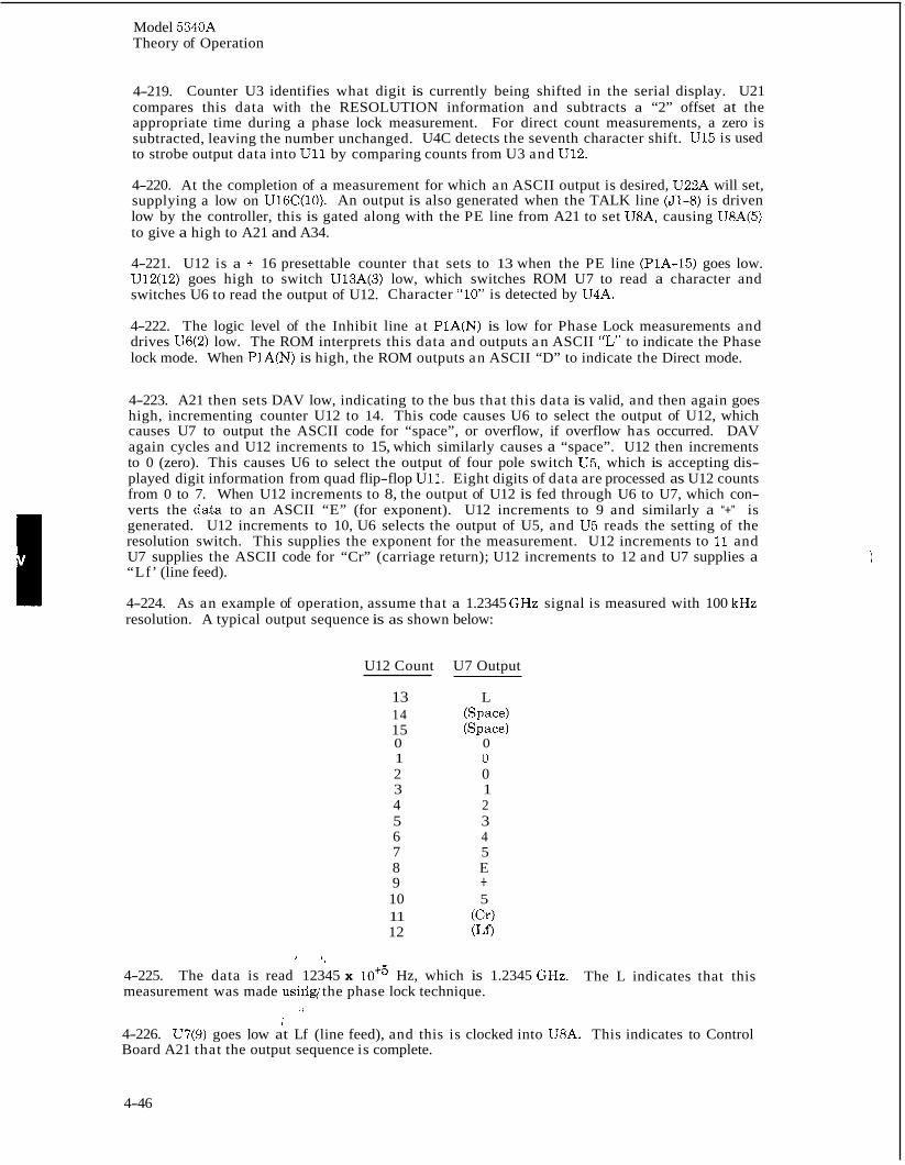
Model 5340A Theory of Operation
4-219. Counter U3 identifies what digit is currently being shifted in the serial display. U21 compares this data with the RESOLUTION information and subtracts a “2” offset at the appropriate time during a phase lock measurement. For direct count measurements, a zero is subtracted, leaving the number unchanged. U4C detects the seventh character shift. U15 is used to strobe output data into U11 by comparing counts from U3 and U12.
4-220. At the completion of a measurement for which an ASCII output is desired, U22A will set, supplying a low on U16C(10). An output is also generated when the TALK line (Jl-8) is driven low by the controller, this is gated along with the PE line from A21 to set U8A, causing U8A(5) to give a high to A21 and A34.
4-221. U12 is a + 16 presettable counter that sets to 13 when the PE line (PlA-15) goes low. U12(12) goes high to switch U13A(3) low, which switches ROM U7 to read a character and switches U6 to read the output of U12. Character “10” is detected by U4A.
4-222. The logic level of the Inhibit line at PlA(N) is low for Phase Lock measurements and drives U6(2) low. The ROM interprets this data and outputs a n ASCII “L” to indicate the Phase lock mode. When PlA(N) is high, the ROM outputs an ASCII “D” to indicate the Direct mode.
4-223. A21 then sets DAV low, indicating to the bus that this data is valid, and then again goes high, incrementing counter U12 to 14. This code causes U6 to select the output of U12, which causes U7 to output the ASCII code for “space”, or overflow, if overflow has occurred. DAV again cycles and U12 increments to 15, which similarly causes a “space”. U12 then increments to 0 (zero). This causes U6 to select the output of four pole switch U5, which is accepting dis- played digit information from quad flip-flop U11. Eight digits of data are processed as U12 counts from 0 to 7. When U12 increments to 8, the output of U12 is fed through U6 to U7, which con- verts the da.ta to an ASCII “E” (for exponent). U12 increments to 9 and similarly a “+” is generated. U12 increments to 10, U6 selects the output of U5, and U5 reads the setting of the resolution switch. This supplies the exponent for the measurement. U12 increments to 11 and U7 supplies the ASCII code for “Cr” (carriage return); U12 increments to 12 and U7 supplies a “Lf’ (line feed).
4-224. As an example of operation, assume that a 1.2345 GHz signal is measured with 100 kHz resolution. A typical output sequence is as shown below:
U12 Count U7 Output
13 L 14 (Space) 15 (Space) 0 0 1 0 2 0 3 1 4 2 5 3 6 4 7 5 8 E 9 + 10 5 11 (Cr) 12 (LO
’ 1 ,
4-225. measurement was made usidgi the phase lock technique.
. J
The data is read 12345 x lot5 Hz, which is 1.2345 GHz. The L indicates that this
/ 4-226. U7(9) goes low at Lf (line feed), and this is clocked into U8A. This indicates to Control Board A21 that the output sequence is complete.
4-46
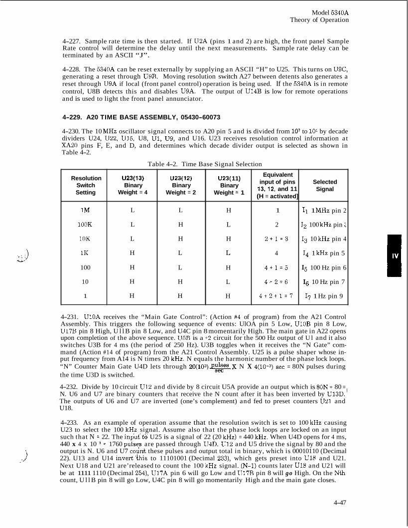
Model 5340A Theory of Operation
j.: .) w
4-227. Sample rate time is then started. If U2A (pins 1 and 2) are high, the front panel Sample Rate control will determine the delay until the next measurements. Sample rate delay can be terminated by an ASCII “J”.
4-228. The 5340A can be reset externally by supplying an ASCII “H” to U25. This turns on U9C, generating a reset through U9B. Moving resolution switch A27 between detents also generates a reset through U9A if local (front panel control) operation is being used. If the 5340A is in remote control, U8B detects this and disables U9A. The output of U14B is low for remote operations and is used to light the front panel annunciator.
4-229. A20 TIME BASE ASSEMBLY, 05430-60073
4-230. The 10 MHz oscillator signal connects to A20 pin 5 and is divided from lo7 to 10’ by decade dividers U24, U22, U15, U8, U1, U9, and U16. U23 receives resolution control information at XA20 pins F, E, and D, and determines which decade divider output is selected as shown in Table 4-2.
Table 4-2. Time Base Signal Selection
Resolution Switch Setting
1M
lOOK
10K
1K
100
10
1
U23(13) Binary
Weight = 4
L
L
L
H
H
H
H
U23(12) Binary
Weight = 2
L
H
H
L
L
H
H
U23( 11) Binary
Weight = 1
H
L
H
H
L
H
Equivalent input of pins
13,12, and 11 (H = activated]
1
2
2 + 1 = 3
4
4 + 1 = 5
4 + 2 = 6
4 + 2 + 1 = 7
Selected Signal
11 1 MHz pin 2
12 100 kHz pin
I3 10 kHz pin 4
I4 1 kHz pin 5
I5 100 Hz pin 6
I6 10 Hz pin 7
I7 1 Hz pin 9
4-231. UlOA receives the “Main Gate Control”: (Action #4 of program) from the A21 Control Assembly. This triggers the following sequence of events: UlOA pin 5 Low, UlOB pin 8 Low, U17B pin 8 High, U l l B pin 8 Low, and U4C pin 8 momentarily High. The main gate in A22 opens upon completion of the above sequence. U5B is a 12 circuit for the 500 Hz output of U l and it also switches U3B for 4 ms (the period of 250 Hz). U3B toggles when it receives the “N Gate” com- mand (Action #14 of program) from the A21 Control Assembly. U25 is a pulse shaper whose in- put frequency from A14 is N times 20 kHz. N equals the harmonic number of the phase lock loops. “N” Counter Main Gate U4D lets through 20(103)*X N X 4(10-3) sec = 80N pulses during the time U3D is switched.
4-232. Divide by 10 circuit U12 and divide by 8 circuit U5A provide an output which is 80N + 80 = N. U6 and U7 are binary counters that receive the N count after it has been inverted by U13D. The outputs of U6 and U7 are inverted (one’s complement) and fed to preset counters U21 and U18.
4-233. As an example of operation assume that the resolution switch is set to 100 kHz causing U23 to select the 100 kHz signal. Assume also that the phase lock loops are locked on an input such that N = 22. The input to U25 is a signal of 22 (20 kHz) = 440 kHz. When U4D opens for 4 ms, 440 x 4 x 10 = 1760 pu1se;s are passed through U4D. U12 and U5 drive the signal by 80 and the output is N. U6 and U7 c o u d these pulses and output total in binary, which is 00010110 (Decimal 22). U13 and U14 invert.this to 11101001 (Decimal 233), which gets preset into U18 and U21. Next U18 and U21 are’released to count the 100 kHz signal. (N-1) counts later U18 and U21 will be at 1111 1110 (Decimal 254), U17A pin 6 will go Low and U17B pin 8 will go High. On the Nth count, U l l B pin 8 will go Low, U4C pin 8 will go momentarily High and the main gate closes.
_ - j
4-47
Model 5340A Theory of Operation
4-234. U3A generates the “N Gate” qualifier for test #2 of the program (N Gate ? has been deter- minted). When the count of U6 reaches 2, U13C(6) goes Low to drive the Q output of U l l A High. This signal is a qualifier for test #7 of the program (N 2 2 ?). BCD to decimal decoder U28 decodes the A6 Search Assembly information which indicates what range the instrument is on. U26, 27, 19, and 20 are comparators that monitor the inverted outputs of U6 and U7 and compares them with the output of U28.
4-235. The purpose of these circuits is to determine if N is within its limits. There are six possible ranges of N for the 5340A. For each range, the instrument selects different passive components so as to obtain a particular gain for the Input Phase Lock Loop. When the instrument is in local control or in remote control and auto range, the signal at U14F pin 13 is High, enabling the N checking circuits. When in remote control and in a particular octave range, the input to U14F goes low disabling the N checking circuits. The six ranges are as follows:
N 64-256
RANGE 1
32-64 2 16-32 3 8-16 4 4-8 5 2-4 6
4-236. A21 CONTROL ASSEMBLY 05340-60021
4-237. The control assembly controls the sequence of activity as a measurement is being made. Refer to Figure 5-3 and note that actions are required and tests are made at various points in the cycle. From the test results, decisions are made and these determine the path through the flow chart.
4-238. U12 is a single pole 16 position switch that selects the desired test and feeds the result out on pin 10. By placing binary 0 through 15 an input pins 11, 13, 14, and 15, U12 selects tests 0 15. For example, having HHHL on pins 15, 14, 13, and 11, respectively, selects test #7. Pin 10 will then output the result of the N 2 2 test from XABO(R). Note that test #O is connected to common. When no test is desired, test #O is selected, giving a known output.
4-239. Similarly U13 is another single pole 16 position switch that selects one of 16 possible actions. For example, placing HLHH into U13 pins 20, 21, 22, and 23, respectively, will select action #11 by pulling U13(13) low. This sets flip-flop U5D-U5C to trigger one-shot U9B. C3 and R6 control the time constant of the one-shot. The output of U9B is fed back to the test selector U12 because the program requires a test for completion of this delay. U8, U5, and U14 are flip-flops that store five of the outputs of U13. All of the outputs of U13 are routed to other areas to initiate a new action. U13(18, 19) are connected to the clock to synchronize actions with the clock signal. UlOB and UlOA are flip-flops that indicate to U12 whether the main gate is opened or closed. Gates U15C and U15A activate the front panel main gate annunciator (A25DSll) when the main gate is opened. U9A is a one-shot that keeps A25DSll on long enough to be visible during short gate times. Note that when no action is desired (for example when a test is being made), action #O is selected, which does nothing.
i 4-240. Read Only Memory (ROM) U4 is a storage device that will supply a predetermined 8-bit output code for each of 32 possible input codes.
4-241. For example when program address HLLLH is on pins 14, 13, 12, 11, and 10, respectively, the output on pins 1 through 7 will be HLLHLLLL, respectively. This will select test #9 and action #O (nothing). Other input codes similarly select other tests and actions. See U4 Truth Table.
4-242. U3 is another ROM that outputs the program address of the next step in Figure 5-3. U1 is a three pole two position syifch that connects, respectively, pins 12, 7 , and 4 to pins 13, 6, and 3 or pins 14, 5, and 2, denending on the test result logic level on pin 1. High selects pins 13, 6, and 3. The three switch lines are used with the two unswitched outputs of U3. The next clock pulse, storage flip-flop U2 transfers this data to ROM’s U3 and U4.
, , ,!
4-48
Model 5340A Theory of Operation
4-243. For example, assume we are completing the step in the fifth symbol in Figure 5-4 marked “Done ? 14”. ROM U3 input on pins 14, 13, 12, 11, and 10 is LLHLH and will output LLHLHHLL on pins 9, 7, 6, 5, 4, 3, 2, and 1, respectively. For the present program address, U4’s output will be HLHH HHHL on pins 1, 2, 3, 4, 5, 6, 7, and 9, respectively.
4-244. U13 will select action #11, (“Start Delay”) by activating U5D, U5C, U9B. U12 will select test #14 (“Done?”) that will drive U12(10) low when the delay is complete. U2’s input on pins 11, 6, 13, 4, and 3 will be LLHLL, respectively, as U1 switches to the Oc OB and OA inputs, because of the low from U12. At the next clock pulse, U2 will feed the LLHLL on its input to U3 and U4.
4-245. U3 will then output LHHH HHLH. U4 will output HLLH HLLL, causing U13 to select action #9 (clear) and causing U12 to select test #8 (“Direct?”).
4-246. If U12 does not sense a DIRect signal, UlZ(l0) will output a H, causing U2 to be fed a LHHHH for the next address. If a DIRect signal is sensed, U1 will select the other three lines of U3, causing U2 to be fed LH HLH for the next address. Note that in the first case, the next action would have been #6 (INH) and in the second case the next action would have been #1 (R. Count). Thus we control the paths through the flow chart.
-
4-247. A22 HIGH FREQUENCY COUNTER ASSEMBLY, 05340-60016
4-248. This assembly (Figure 8-29) contains the first two decade counters of the decade counting chain. Logic switch U8 selects either the direct count or the HI Z input and provides an output which is shaped by Schmitt trigger U9. Data switch U3B selects between the VCO input and the check signal. Data switch U3A selects the input for main gate/decade counter U2B. U6 is the main gate flip-flop, which is controlled by differential amplifier Q4 and QlO. Q4-QlO converts the TI’L signal from A20 to the EECL logic levels required by U6. The + 10 output of U2A feeds 7 2 circuit U7, which drives U4 after passing through EECL to TTL level shifter circuitry Q17-Q20.
4-249. The outputs of U2 and U7 are EECL (0 to -0.6V). Q13 through Q16 convert this to ECL (0.85 to -1.5V). U1 shifts the ECL to TTL (approximately +2.5V to OV). U5 receives the four line output from each decade counter and multiplexes the information (transfers it one line at a time) to A23 after counting has been completed. The logic revels on U5 (pins 3 and 13) determine which line is outputted.
4-250. The output of U7 is EECL and connects to emitter follower Q17 which in turn feeds differential amplifier Q18-Q20. The differential amplifier drives saturated switch Q19 giving TTL levels at the collector of Q19. This is fed to +5 circuit U4 and also outputed via U5. CR1 is a catcher diode to keep Q19 from complete saturation. Differential amplifiers Ql-Q7, Q2-Q8, etc., shift from TTL control levels to the EECL needed for the IC’s. The RC network (C3, R4, etc.) speeds up the transition time.
4-251. A23 COUNT REGISTER ASSEMBLY, 05340-60030
4-252. When the m(para l le1 entry) line at A23, pin K is high, U7 receives inputs from A23, pin 13 via U18A, U15B, and U14C. This input is derived from A22U4. U7 through U2 are a series of decade counters and shift registers with U2 1 being the most significant digit. When the main gate on A22 is open U7, U6, U5, U4, U3, and U2 will count the output of A22U4. This counter chain will contain the 102 to 107 digits of the meas- urement. PE goes high when the main gate on A22 closes. The output of the two least significant digits on A22 must then be shifted 1-bit at a time into A23U8 and U9 through A22U5. U16A and B generate the 00, 01, 11, and 10 code necessary to shift the BCD data for the 100 and 101 digits into U8 and U9. , ,
4-253. By pulling PE low,, tpe control board A21 initiates shifting of the BCD data in A23U2 through A23U9 into A24. , Ih the direct count mode, the information is fed in directly. In the phase lock mode, it is qecessary to subtract 20 MHz from the stored information because of the 20 MHz IF circuit. Flexibility is obtained by being able to add or subtract. UlO, U11, U21, U18, U19B, and U20 comprise a BCD adder/subtractor. A BCD “2” is generated on A19 and routed
Refer to Figure 8-30 for the schematic diagram.
4-49
Model 5340A Theory of Operation
into A23U20. Using range information and the resolution switch setting, A19 determines when the “2” must be inserted as the eight columns of BCD information are shifted into A24.
4-254. U21A and U21B are activated for addition and U18D is used for subtraction. The carry information from U19B is sent into the carry input of the first BCD adder U10. UlA, UlB, and U12 determine when overflow occurs and activate flip-flop U19A to turn on the overflow light. U17A and U17B turn on the lock and direct annunciator lamps as determined by circuits on A21. U11 is a binary to BCD converter.
4-255. A24 DISPLAY REGISTER ASSEMBLY, 05340-60019
4-256. This Display Register (Figure 8-31) accepts and stores information to be displayed on the display tubes and the annunciator lights.
4-257. U4 receives BCD inputs (weighted 8, 4, 2, and 1) from A23 and supplies outputs to U l l , U17, U9, and U16. U3, UlOB, and U3B detect zeroes and store a TTL high in U1 whenever a zero is detected. U2 determines how many insignificant (leading) zeroes exist and outputs a binary code. U18 is a binary to decimal converter that receives the resolution switch information and determines proper positioning of the decimal point. This information is coupled with leading zero information to activate the appropriate blanking circuitry on A25. When shifting is com- plete, the BCD “1” information is stored in U16, with the Q8 output holding the loo information and the Q1 output holding the 108 information. Similarly U9, U17, and U11 contain the BCD “Z”, “4”, and “8” information, respectively.
4-258. A25 DISPLAY ASSEMBLY, 05340-60020
4-259. The Display Assembly (Figure 8-32) consists of display tubes DS1 through DS8, display tube drivers U1 through U8, decimal decoder U9, units decoder U10, units indicators DS15-17, annunciators DS9 through DS14, and annunciator drivers Q1 through Q6.
4-260. The display tube drivers U1 through U8 are four-line BCD to decimal decoders. The table below shows the decoder truth table.
I 4-261. When a particular output line of a decoder is on, the line is low to allow the corresponding digit on the display tube to light. As an example of operation, assume that U8 receives a BCD input of D = L, C = H, B = L, and A = H. In this case, decoder U8 drives the 5 output low to light the 5 digit in DS8, the loo display tube. The anodes of the 100, 101, and 102 display tubes receive +175 volts from the power supply through R5, R7, and R9. The remaining anodes are connected to the blanking board A26.
4-262. The decimal point decoder U9 receives four-line BCD from A24 and drives the left decimal point in the display tube. The decimal point decoding is not proportional, for example, when the BCD input is LLLL, the 0 output of U9 goes low to light the left decimal point in the lo3 display tube. The theory of operation for the BCD decoding is described in the theory for A24. To determine the required BCD input for a particular decimal point, the schematic (Figure 8-32) and truth table can be used. For example, to light the decimal point in the 105 display tube,, U9(13) (decimal 4) should go low which requires a DCBA input of LHLL.
4-263. The units decoder U10 is similar to the decimal point decoder U9. The GHz indicator will light when the BCD input is equivalent to either 0, 3, 4, or 9. Similarly, the MHz indicator is driven by the 1 or 7 output of U10. When the BCD input to U10 is equivalent to decimal 5, the kHz light will light. For the theory of operation for this BCD input, refer to the description for A24.
4-264. The annunciators DS9 through DS14 are controlled by inputs from A24. Emitter follower Q7 and voltage divider R24 kind R25 establish a +2 volt bias for Q1 through Q6 and also for the blanking board. As an example of operation, when system lock occurs, A24 supplies a low to the emitter of Q2 to allow &2 to conduct and light DS10. Zender diode CRl drops the 175 volts by ap- proximately 25 volts to operate DS9 through DS17.
4-50
i
I Model 5340A Theory of Operation
4-265. A26 BLANKING ASSEMBLY, 05340-60037
4-266. The Blanking Assembly (Figure 8-32) is controlled by logic circuits on A25 and controls the +175V supply to the display tube(s) that require blanking thus suppressing insignificant zeroes. For example, with a TTL low on the emitter of Q5, Q5 conducts to turn on QlO which in turn supplies +175V to the display tube. Similarly the other four tubes are controlled.
4-267. POWER SUPPLIES
4-268. The power supplies include Time Base Power Supply A33 (part of Option O O l ) , +5 Volt Regulator A32, +15 Volt Regulator A29, -15 Volt and +175 Volt Regulator A28, and - Volt Regu- lator A31. Since the power supplies use similar regulator IC’s and circuit arrangements, the simplest will be described first and the applicable circuit theory will suffice for the remaining regulator units.
4-269. A33 Time Base Power Supply Assembly, 05340-60039, (Part of Option 001)
4-270. The Time Base Power Supply (Figure 8-35) provides +21 volts unregulated a t approxi- mately 100 mA and +I1 volts regulated power at approximately 25 mA to optional oscillator A18. The +21 volt supply consists of full-wave rectifier A33CR1, A33CR2, and A33Cl. The regulated +11 volt supply is made up of A33CR3, A33CR4, A33C2, A33U1, and associated circuitry. 1 A33U1, the voltage regulator IC has the equivalent circuit shown in Figure 4-52.
4-271. The regulator consists of a current source, voltage reference amplifier, error amplifier, current limiter, and series pass transistor. The current source, Zener diode, and voltage reference amplifier provide a constant 7.2 volt reference output (Vref) for the noninverting input of the difference amplifier. Th‘e inverting input of the difference amplifier senses the power supply output voltage through vOltage divider A33R7, A33R8, and A33R9 (see schematic for A33). A33R8 is adjusted to set thk butput voltage. An example of regulation is as follows. If the output voltage decreases, the voldage at A33R8 and the inverting input (Ul pin 2) also decreases. This drives the error amplifi‘er output more positive which biases the series pass transistor to decrease its impedance. When the impedance of the series pass transistor decreases, the output voltage tends to increase to regulate the output.
j -. 2
4-51
Model 5340A Theory of Operation
4-272. The current limiter consists of A33R4, A33R5, A33R6, and the current limiter transistor in the IC (see Figure 4-52). A33R6 determines the current limit point and A33R4 and A33R5 determine the foldback current limit operation. When the drop across R6 is sufficient to forward bias the current limit transistor (Figure 4-52), the current limit transistor draws base current away from the series pass transistor thereby reducing the output voltage and limiting the current. The foldback current limiting provides a further reduction in current to prevent excessive power dissipation in the IC. A33R2 provides temperature compensation and supplies the reference voltage at A33U1(4) to the noninverted input at A33U1(3). A33C4 bypasses Zener diode noise on Vref. A33C5 provides frequency compensation to prevent high frequency oscillations.
Figure 4-52. Equivalent Regulator Circuit
V+ ERROR SERIES PASS a AMPL TRANSISTOR I - a -
FREO COMP VC 9 7
4 b a "REF - 4
CURRENT SOURCE
a - VOLTAGE 5
REF AMPL V- \ ./ /
CURRENT LIMITER
4-273. A32 +5 Volt Regulator Assembly, 05340-60023
4-274. A32 (Figure 8-34) contains two +5 volt regulators, one for the RF circuits and the other for the digital circuits (+5 DG). The RF +5 volt regulator supplies approximately 32 mA and con- sists of preregulator A32Q1, A32Q2, A32U1, and series pass transistor A32Q5. The digital +5 volt regulator supplies approximately 3 amperes and consists of regulator A32U2, driver A32Q3 ' and series pass transistor Q2 which is mounted on the rear panel of the instrument. Connections from A32 to QZ are made through the power supply mother board A30 and three wires to the rear panel.
4-275. +5 VOLT RF REGULATOR (PART OF A32). To prevent drift and instability in the RF circuits of the 5340A, tKe'+b volt RF regulator in A32 (Figure 8-34) uses a preregulator to achieve the required regulation and low ripple voltage. A32CR1 and A32CR2 establish a con- stant current through A32QV and A32CR4. Zener diode A32CR4 provides a constant 11 volt out- put which is connected to.'the Vc input of A32U1 via a darlington transistor pair A32Q2A and B. A32C1 filters out noise'generated in the Zener diode. The operation of A32U1 is similar to that described for the Time Base Power Supply A33 (see Paragraph 4-270). The reference supply voltage for A32U1 is derived from the +15 volt supply A29.
4-52
Model 5340A Theory of Operation
4-276. In the event that the +15 volt reference fails or falls below 11 volts, A32CR3 conducts to turn off A32Q2 thereby disabling the supply. This prevents A32U1 from locking in the off position. The series pass transistor in A32U1 drives A32Q5 to handle the larger current require- ments of the regulator. A32R17 sets the current limit point and A32R16 and R18 set the current foldback characteristics.
4-277. +5 VOLT DIGITAL REGULATOR (PART OF A32). The +5 volt digital regulator (Figure 8-34) is similar to the +5 volt RF regulator except for no preregulator, additional series pass transistors, and two current limit circuits. In order to handle the 3 amp load, an external series pass transistor (Q2) and driver (A32Q3) are provided. A32R9 serves as the collector load for A32Q3. The operation of U2 is similar to that described in Paragraph 4-270. A32R10 provides current limiting for the IC. For example, if Q2 opens, the series pass transistor in A32U2 and A32Q3 would be seriously overloaded. In this case, the drop across A32R10 drives A32U2 into current limiting. A32Q4 provides current limiting for loads above 3 amperes. When the drop across A32R13 and R15 forward biases A32Q4, A32U2 is driven into the current limit mode. The collector of A32Q4 connects to the compensation input (see Figure 4-52) which is in parallel with the current limit amplifier in the IC. The current foldback circuit is made up of A32Rll and R12. A32R14, A32CR6, and A32C10 provide regulation for the current foldback point to prevent line voltage variations from changing the foldback characteristics. A32CR5 and A32C9 provide ripple filtering for the current foldback circuit.
4-278. A29 +15 Volt Regulator Assembly, 05340-60025
4-279. The +15 volt regulator (Figure 8-33) is similar to the +5 volt RF regulator described in Paragraph 4-275. The supply provides approximately 170 milliamperes. The preregulator is composed of A29Q1, A29Q2, and A29CR1-CR3. A29Q3 is the series pass transistor. Current limiting is set by A29R7 and A29R10. A29R6 and A29R9 set the current foldback characteristics. A29R5 adjusts the output voltage.
4-280. A28 -15 Volt and t175 Regulator Assembly, 05340-60022
4-281. The -15 volt regulator (Figure 8-33) supplies about 180 milliamperes and consists of a preregulator, regulator, series pass transistor and driver, and current limit circuits. A28Q1 and A28Q3 serve as a constant current source for A28CR2. Zener diode A28CR2 establishes a con- stant 19.6 volts for the regulator reference input. R5 sets the proper current input for the regulator reference. A28U1 is a negative supply voltage regulator similar to the positive voltage regulator previously discussed. The reference current input at A28U1 flows internally through the IC to pin 1 and A28R6 and A28R7. Adjusting A28R7 sets the output supply voltage. The boost output a t A28U1(7) drives Q7 and QlO to regulate the output voltage. A28C4 provides com- pensation to prevent high-frequency oscillation. Current limiting for the IC is determined by A28Rll. A28R16 is the current limit resistor and works in conjunction with A28Q8. When the current limit point is reached, the drop across A28R16 turns on A28Q7 which diverts drive current from A28Q10. A28R13 and A28R14 determine the current foldback limiting characteristics.
I 4-282. The +175 volt regulator provides +175 volts at about 28 milliamperes to drive the display tubes in A25. Since no filter capacitors are used for rectifier A30CR1, a pulsating dc is developed for driving the display tubes. A28Q2, A28R2, and A28CR1 serves as a current source for A28CR3 and A28CR4. A28CR3 and A28CR4 provide the +175 volt reference for A28Q4. A28Q4 drives A28Q6 which serves as the series pass transistor. Current limiting is set by A28R15 and the current foldback limiting, chgracteristics are determined by A28R8 and A28R10. When the drop across A28R15 is sufficient ' t o turn on A28Q9, A28Q9 diverts current from A28Q4 thereby reducing the output voltagb to maintain a constant current. With overloads, the voltage across A28R8 and A28RlO bias3siA28Q9 to conduct further to reduce the output current below the current limit point set ,by A28R15. This is foldback action and prevents excessive power dis- sipation in the regulator. A28R9 suppresses as oscillations. A28C6 filters out the pulsating dc from A28Q9 to prevent A28Q9 from conducting at the peak levels of the pulsating dc.
-I
4-53
Model 5340A Theory of Operation
4-283. A31 -5 Volt Regulator Assembly, 05340-60024
4-284. The -5 volt regulator assembly (Figure 8-34) consists of two supplies, one for the RF circuits (-5V) in the 5340A and the other for the digital circuits (-DG). The supply for the RF circuits provides about 190 milliamperes and the digital supply provides approximately 1.1 amperes. The RF supply consists of a preregulator A31Q1, A3lQ2, A31Q3, and A31CR1. A31Q8 is the series pass transistor and A31Q4 serves as the regulator driver. The circuit is similar to the -15 volt regulator previously described. A31R17 sets the current limit point and A31R13 and A31R14 determine the current foldback characteristics. The regulator for the digital circuits consists of A31U2, A31Q6, A31Q7, and Q1 which is mounted on the rear panel. Connection to Q1 is made via the power supply motherboard A30. This regulator is similar to the -5 volt regulator previously discussed except that no preregulator is used.
4-285. A34 Theory of Operation, 05340-60067 (Part of Option 011)
4-286. There are two basic modes of remote operation for the 5340A, they are TALK and LISTEN. The three wire handshake must occur before the instrument can function in either mode. A35S6 is the “Talk Always-Addressable” switch. In the “Talk Always” mode, A35S6 keeps the talk flip- flop (U7) in the set condition. This allows the 5340A to communicate with a simple listener that doesn’t have addressing capability. When A35S6 is in the “Addressable” position, the instrument can be either a talker or listener. A low on IFC is a direct clear, which resets U6 and U7.
4-287. Talk Mode
4-288. In the first sequence of the talk mode, the 5340A is addressed to talk. At this time ATN is Low and the controller sends data via DIOl through DI07. Switches A35S1 through A35S5 establish the 5-bit binary code which is an arbitrarily designated address of the 5340A. U14 com- pares this code to the data on lines DIOl through D105 and outputs a high when coincidence oc- curs. D106 and D107 carry the information which determines whether the instrument will func- tion as a talker or listener, this information is decoded by U6 and U7. The controller set DAV Low, this signal is delayed by R4, C2, and R5, C3 which allow transients to die down. As C3 charges through R5, UlD(11) will remain high. This enables U5A to provide the clock pulse for U6 and U7. U5A also receives the IFC signal which must be high. ATN low will enable the RFD driver UlOC and the DAC driver U19B. RFD will go low and DAC will go high, completing the three wire handshake. (See Section I1 for a more detailed explanation of the handshake). When U5A clocks U6 or U7, only one will set. When Talk Flip-Flop U7 is set, UllB(6) goes high enabling the DIOl through D107 drivers UZA, B, C, D, U3A, B, C, D, and DAV driver U4D. UllB(6) will also enable the RFD and DAC listeners U13C, D. U13C provides the qualifier for test #3 of the pro- gram (HRFD ?) and U13D provides the qualifier for test #10 (HDAC ?).
4-289. The second sequence of the Talk Mode is data outputting. After handshaking, the con- troller sets ATN high to disable the RFD and DAC gates (UlOB,C). The instrument can now out- put measurements it has taken via the DIOl through D107 drivers. SRQ (Service Request) is an output driven low by UlOD when the instrument has been programmed to wait in the output phase of it’s operating cycle until addressed to output.
4-290. Listen Mode
4-291. In the first sequence of the listen mode, the 5340A is addressed to listen. It is identical to the address sequence of ,the ,talk mode, with the exception that command on the DIOl through D107 lines now tells the instrument to listen. U6 is set and U5B(8) goes low for the duration of DAV’s delay. U5B(8) genel;a es the LOAD signal.
4-292. The second seqpence is listening. UllC(8) enables the RFD and DAC drivers (UlOB,C) to allow the instrument in this mode of operation to have control of these lines. The DAV driver (U4D) is disabled. At this point in the sequence, the instrument is ready to accept data.
I F
4) .
4-54
Model 5340A Maintenance and Service
SECTION V
MAINTENANCE AND SERVICE
5-1. INTRODUCTION
5-2. This section contains maintenance and service information including a table of assemblies, recommended test equipment, in-cabinet performance check, troubleshooting, and adjustment procedures.
5-3. ASSEMBLY DESIGNATIONS
5-4. Table 5-1 lists the designation, nomenclature, and Hewlett-Packard part number of assemblies used in the 5340A.
5-5. TEST EQUIPMENT
5-6. Table 5-2 lists test equipment recommended for maintaining and checking the performance of the counter. Test equipment having equivalent characteristics may be substituted for the equipment listed.
5-7. POZlDRlV SCREWDRIVERS
5-8. Pozidriv screws are used in this instrument. To avoid damage to the screw slots, a pozidriv screwdriver (HP Part Number 8710-0900) should be used.
5-9.. ADJUSTMENTS AND IN-CABINET PERFORMANCE CHECK
5-10. Figure 5-2 contains adjustment procedures for the 5340A. Adjustments should be made when the necessity is established by the performance test or when components are replaced that affect an adjustment. If all adjustments are to be performed, they should be performed in the order listed. Table 5-3 contains the in-cabinet performance check.
5-11. BLOWER FAN CONFIGURATION
5-12. The cooling fan in the 5340A is a n exhaust fan, not an intake type. The fan discharges air out of the rear of the instrument. If the flow of air was reversed, the heat generated by the fan would preheat the intake air and tend to raise the internal temperature of the instrument.
5-13. K05-5340A DESCRIPTION
5-14. The K05-5340A Feed Forward Simulator or equivalent is required to adjust A8 and A9. During the adjustment procedure, A7 is removed and the K05-5340A is installed in XA7. The K05-5340A provides a variable simulated feed-forward signal to A10 and A12. The K05-5340A Feed-Forward Simulator can be purchased through your local Hewlett-Packard Sales and Service Office. An equivalent of the K05-5340A can be fabricated with the following parts and schematic diagram (see Fi uke 5-1).
5-15. pin 5.
F An alternate m'ethod is to connect a 0-15V dc power supply from XA7 pin 10 to XA7
- j
5- 1
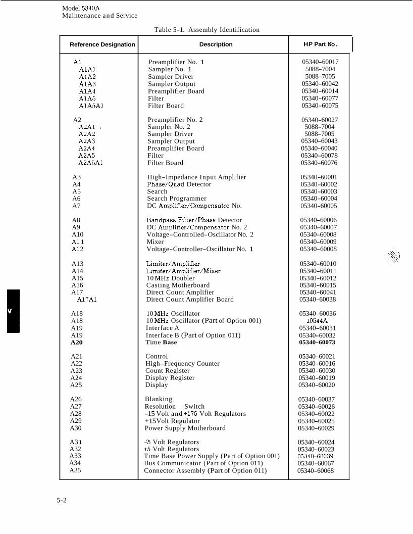
Model 5340A Maintenance and Service
Table 5-1. Assembly Identification
Reference Designation
A1 A l A l A1A2 A1A3 A1A4 A1A5 AlA5AI
A2 A2A1 A2A2 A2A3 A2A4 A2A5 A2A5A1
A3 A4 A5 A6 A7
A8 A9 A10 A1 1 A1 2
A13 A14 A15 A16 A17
A17A1
A18 A18 A19 A19 A20
A21 A22 A23 A24 A25
A26 A27 A28 A29 A30
A3 1 A32 A33 A34 A35
Description
Preamplifier No. 1 Sampler No. 1 Sampler Driver Sampler Output Preamplifier Board Filter Filter Board
Preamplifier No. 2 Sampler No. 2 Sampler Driver Sampler Output Preamplifier Board Filter Filter Board
High-Impedance Input Amplifier Phase/Quad Detector Search Search Programmer DC Amplifier/Compensator No.
Bandpass Filter/Phase Detector DC Amplifier/Compensator No. 2 Voltage-Controlled-Oscillator No. 2 Mixer Voltage-Controller-Oscillator No. 1
Limiter/Amplifier Limiter/Amplifier/Mixer 10 MHz Doubler Casting Motherboard Direct Count Amplifier Direct Count Amplifier Board
10 MHz Oscillator 10 MHz Oscillator (Part of Option 001) Interface A Interface B (Part of Option 011) Time Base
Control High-Frequency Counter Count Register Display Register Display
Blanking Resolution Switch -15 Volt and +175 Volt Regulators +15 Volt Regulator Power Supply Motherboard
1.5 Volt Regulators +5 Volt Regulators Time Base Power Supply (Part of Option 001) Bus Communicator (Part of Option 011) Connector Assembly (Part of Option 011)
HP Part No. I 05340-60017 5088-7004 5088-7005
05340-60042 05340-60014 05340-60077 05340-60075
05340-60027 5088-7004 5088-7005
05340-60043 05340-60040 05340-60078 05340-60076
05340-60001 05340-60002 05340-60003 05340-60004 05340-60005
05340-60006 05340-60007 05340-60008 05340-60009 05340-60008
05340-60010 05340-60011 05340-60012 05340-60015 05340-60041 05340-60038
05340-60036 10544A
05340-60031 05340-60032 05340-60073
05340-60021 05340-60016 05340-60030 05340-60019 05340-60020
05340-60037 05340-60026 05340-60022 05340-60025 05340-60029
05340-60024 05340-60023 05340-60039 05340-60067 05340-60068
5-2
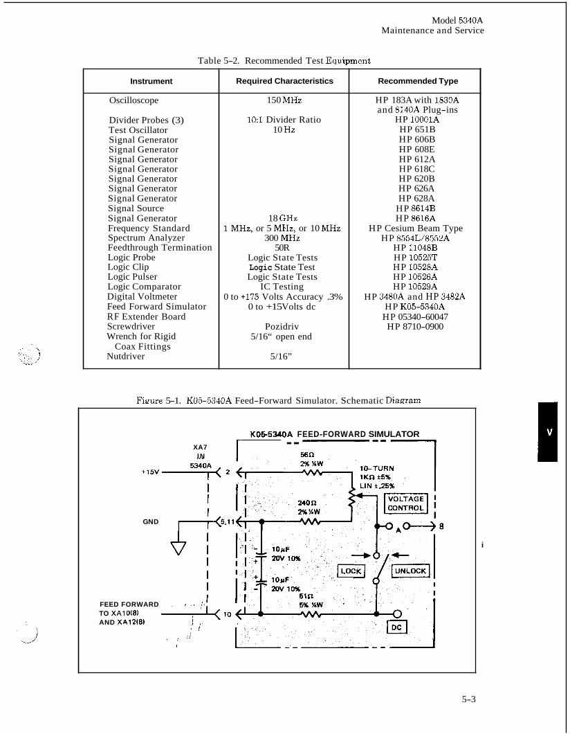
Table 5-2. Recommended Test Euui
Model 5340A Maintenance and Service
lent
Instrument
Oscilloscope
Divider Probes (3) Test Oscillator Signal Generator Signal Generator Signal Generator Signal Generator Signal Generator Signal Generator Signal Generator Signal Source Signal Generator Frequency Standard Spectrum Analyzer Feedthrough Termination Logic Probe Logic Clip Logic Pulser Logic Comparator Digital Voltmeter Feed Forward Simulator RF Extender Board Screwdriver Wrench for Rigid
Coax Fittings Nutdriver
Required Characteristics
150 MHz
1O:l Divider Ratio 10 Hz
18 GHz 1 MHz, or 5 MHz, or 10 MHz
300 MHz 50R
Logic State Tests Logic State Test Logic State Tests
IC Testing 0 to +175 Volts Accuracy .3%
0 to +15 Volts dc
Pozidriv 5/16“ open end
5/16”
Recommended Type
HP 183A with 1830A and 8140A Plug-ins
HP 10001A HP 651B HP 606B HP 608E HP 612A HP 618C HP 620B HP 626A HP 628A
HP 8614B HP 8616A
HP Cesium Beam Type HP 8554L/8552A
HP 11048B HP 10525T HP 10528A HP 10526A HP 10529A
HP 3480A and HP 3482A HP K05-5340A
HP 05340-60047 HP 8710-0900
Figure 5-1. K05-5340A Feed-Forward Simulator. Schematic Diagram
+15V
GN D
FEED FORWARD TO XA1 O ( 8 ) AND XAlZ(8)
K055340A FEED-FORWARD SIMULATOR -- 56sl
XA7 -- IN
i
5-3
Model 5340A Maintenance and Service
Figure 5-2. Adjustment Procedures
1.
a.
b.
C.
d.
e.
f.
g.
2.
a.
b.
C.
d.
e.
f.
g.
3.
a.
b.
C.
d.
e. f.
g.
h.
i.
j.
POWER SUPPLY ADJUSTMENTS (05340-6001 2)
-15V Adjustment. On A28 -15V Regulator board (05340-60022), connect voltmeter to TP2. Connect other lead to chassis. Adjust potentiometer A28R7 for -15.00 i0.05 volts indication.
+15V Adjustment. On A29 +15V Regulator board (05340-60025), connect voltmeter lead to TP2. Adjust potentiometer A29R5 for t15.00 k0.05 volts indication.
-5V RF Supply Adjustment. On A31 -5V Regulator board (05340-60024), connect voltmeter probe to TP2. Adjust potentiometer A31R9 for -5.00 i0.05 volts indication. A31R9 is near TP1.
-5V Digital Supply Adjustment. On A31 -5V Regulator board (05340-60024), connect voltmeter probe to TP3. Adjust potentiometer A31R2 for -5.00 i0.05 volts indication. A31R2 is near the front edge of the board
+5V RF Supply Adjustment. On A32 +5V Regulator board (05340-60023), connect voltmeter to TP1. Adjustment potentiometer A32R6 for + L O O *0.05 volts indication. A32R6 is adjacent to TP1.
+5V Digital Supply Adjustment. On A32 +5V Regulator board (05340-60023), connect voltmeter to TP2. Adjust potentiometer A32R3 for t5.00 i0.05 volts indication. R3 is adjacent to TP2, and near the front edge of the board.
Time Base Power Supply (t11V) Adjustment (Option 001). On A33 +11V Regulator board (05340-60039), connect voltmeter to TP1. Adjust potentiometer A33R8 for +11.00 i0.05 volts.
HIGH IMPEDANCE AMPLIFIER ADJUSTMENT (05340-60001)
Connect a 608 Signal Generator to “10 Hz to 250 MHz” input BNC on 5340A using a 50 ohm feedthru termination. Set 608 to 100 MHz at 100 mV rms. (283 mV p-p) (-7 dBm).
Set 5340A RANGE switch to 10 Hz -250 MHz and resolution switch to 100 Hz.
On A3 Input board (05340-60001), adjust potentiometer A3R10 for a stable count.
Decrease input signal level and adjust A3R10 for a stable display.
Continue to decrease input signal level and adjust A3R10 for maximum sensitivity.
Verify that the 5340A properly measures input signals of 50 mV rms or less (140 mV p-p) (-14 dBm).
50Q DIRECT COUNT ADJUSTMENT (05340-60041)
Connect a 608 Signal Generator to the type N connector on the 5340A. Set the generator to 100 MHz at -25 dBm (12.6 mV rms) (35.6 mV p-p). Set 5340A RESOLUTION switch to 100 Hz and the RANGE switch to the 10 Hz to 18 GHz position.
Remove the four screws attaching the cover on the A17 (05340-60041) Direct Count Assembly. Verify that the knurled screw is firmly finger tight, securely holding board in position. Replace cover.
Adjust the threshold detector potentiometer A17A1 R22 full counterclockwise. This is accessible through the front hold in the A17 casting cover.
Adjust sensitivity potentiometer A17A1 R11 for a stable display. Decrease signal generator output and again adjust A17A1 R11 for a stable display. Continue to decrease signal generator output and adjust A17A1 R11 until maximum sensitivity is achieved
Increase generator output until a stable reading is displayed.
Rotate threshold detector pofentiometer A17A1 R22 fully clockwise, observing a display of all zeros.
Increase signal generator output by 1 dB from the level obtained in step h.
k. Rotate threshold detector pot$;lhometer A17A1 R22 sufficiently counterclockwise until correct reading is always displayed. I
1. Verify that sensitivity is a t least -32 dBm. If not, perform A22R52 adjustment (step 11).
5-4
Model 534QA Maintenance and Service
Figure 5-2. Adjustment Procedures (Continued)
k
5-5
Model 5340A Maintenance and Service
Figure 5-2. Adjustment Procedures (Continued)
4.
a.
b.
C.
d.
e.
f.
5.
a.
b.
C.
d.
e.
f.
g. h.
i.
j. k.
1. n.
n.
10 MHz DOUBLER ADJUSTMENT (05340-60012)
Remove the cover on the large casting by removing 12 screws. Locate A15 10 MHz Doubler Board (05340- 60012). Do not remove board. Do not use an extender board.
Set Dual Trace Oscilloscope for sensitivity of 0.05 V/cm with a sweep time of 0.1 psec/cm. Set Channel B polarity to “-” up and A to “+” up.
Using 1O:l divider probes, connect oscilloscope Channels A and B to XA15(1) and XA15(2). Switch oscillo- scope display control to A plus B. Adjust capacitor A15C3 for maximum amplitude of the signal on the oscilloscope.
Adjust A15C13 and A15Cll for maximum amplitude on the oscilloscope. Since these two adjustments interact, repeat the procedure several times to achieve the optimum setting.
Switch Oscilloscope to A&B only. Verify that signals are of approximately the same amplitude.
ADJUSTMENT OF A8 (05340-60006) AND A9 (05340-60007)
Remove A7 (05340-60005) board and install Feed-Forward Simulator K05-5340A in XA7. See Paragraph 5-13 for description of K05-5340A.
Set KO5 switch to LOCK.
Using VTVM, measure feed-forward voltage (FF) from XA7(10) to ground. Adjust VOLTAGE CONTROL on K05-5340A for a 9.00 volt reading.
Adjust A8R13 (LEVEL) and A9R4 (GAIN) fully clockwise.
Set controls on Oscilloscope to:
CHANNEL A to 0.02 V/cm; AC coupled; + up TRIGGER to internal; - slope; AC MODE to Norm SWEEP to 50 ps/cm DISPLAY to CHANNEL A
Using 1 O : l divider probe, connect Channel A of the oscilloscope to XAll(1) (MIX SIG. 20 kHz).
Adjust Channel A position to center the sine wave on the screen. If a large misadjustment exists, no sine wave will be displayed on Channel A. If necessary, adjust A9R1 (OFFSET) until a sine wave is displayed.
Using BNC to alligator clip adaptor, connect “VCO #1 to Counter” signal (available a t A16J6) to INPUT BNC on the 5340A. Set RANGE switch to “10 Hz to 250 MHz”. Display should be between 100 to 185 MHz. Vary the KO5 VOLTAGE CONTROL potentiometer so that counter displays a range of frequencies from 100 to 185 MHz and note the point of maximum distortion of the scope display. Adjust KO5 potentiometer for maximum distortion of the sine wave and the counter display within the 100 to 185 MHz range.
Set the scope sweep to 5 ps/cm.
Back off A9R4 (GAIN) ccw just enough for minimum side jitter (phase noise) of the sine wave. It may be helpful to set the scope sweep to 2 ys/cm and 1 ps/cm to observe parts of the wave.
Connect a DVM to “TL Control” voltage, available at XA9(15).
Vary VOLTAGE CONTROLon h05 so counter display ranges from 100 to 185 MHz, and note the point “TL Control” voltage is maximup. Record this voltage. Vmax =
Find the point in the 100 -18dMHz range where “TL Control” voltage is minimum. Record this voltage. Vmin =
~
I
5-6
Model 5340A Maintenance and Service
Figure 5-2. Adjustment Procedures (Continued)
0.
P.
q. r. S .
Calculate the average value of the two voltages measured in steps n and o above by finding the algebraic sum of the voltages in step n and in step o and dividing by 2.
Example 1: Vmax = t0.544 volts Example 2: Vmax = 0.456 volts
vmin = +0.012 volts Vmin -0.102 volts
t0.556 + 2 = +0.278 volts +0.354 + 2 = +0.177 volts
Move oscilloscope probe to XAlO(7) (T.L. Control). Change oscilloscope controls: Channel A to 0.2 V/cm dc coupled, SWEEP to 5 ms/cm. Adjust the oscilloscope Channel A position so zero volts dc is at the center of the screen. Set KO5 switch to UNLOCK. Adjust A9R1 (OFFSET) so that the wave form display is symmetrical about the value calculated in step p. For Example 1, the ramp should be centered at t0.278 volts. Since the center of the screen is 0 volts, +0.278 volts is .139 cm above the center of the screen (+0.278V + 2V/cm). The 2V/cm is due to the 1O:l divider probe and the O.ZV/cm sensitivity (.2V/cm x 10 = 2V/cm).
5-7
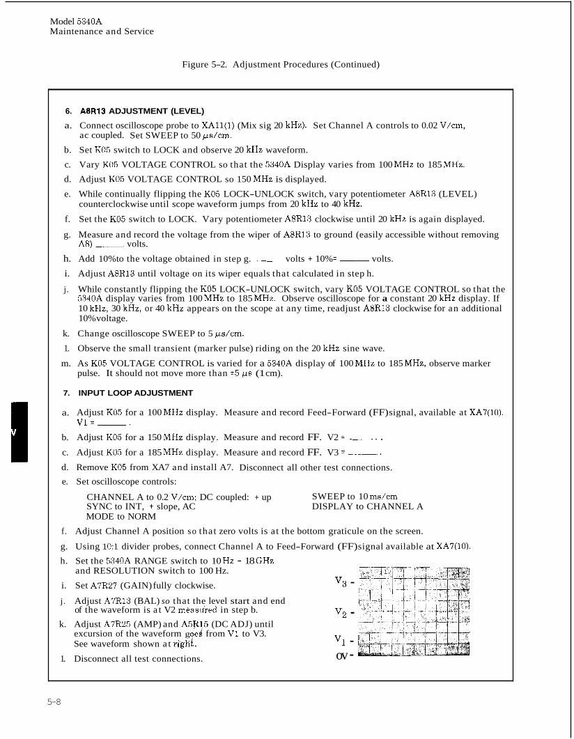
Model 5340A Maintenance and Service
Figure 5-2. Adjustment Procedures (Continued)
6. A8R13 ADJUSTMENT (LEVEL)
a. Connect oscilloscope probe to XAll(1) (Mix sig 20 kHz). Set Channel A controls to 0.02 V/cm, ac coupled. Set SWEEP to 50 p d c m .
b. Set KO5 switch to LOCK and observe 20 kHz waveform.
c. Vary KO5 VOLTAGE CONTROL so that the 5340A Display varies from 100 MHz to 185 MHz.
d. Adjust KO5 VOLTAGE CONTROL so 150 MHz is displayed.
e. While continually flipping the KO5 LOCK-UNLOCK switch, vary potentiometer A8R13 (LEVEL) counterclockwise until scope waveform jumps from 20 kHz to 40 kHz.
f. Set the KO5 switch to LOCK. Vary potentiometer A8R13 clockwise until 20 kHz is again displayed.
g. Measure and record the voltage from the wiper of A8R13 to ground (easily accessible without removing A8) ___ volts.
h. Add 10% to the voltage obtained in step g. ___ volts + 10% = ~ volts.
i. Adjust A8R13 until voltage on its wiper equals that calculated in step h.
j. While constantly flipping the KO5 LOCK-UNLOCK switch, vary KO5 VOLTAGE CONTROL so that the 5340A display varies from 100 MHz to 185 MHz. Observe oscilloscope for a constant 20 kHz display. If 10 kHz, 30 kHz, or 40 kHz appears on the scope at any time, readjust A8R13 clockwise for an additional 10% voltage.
k. Change oscilloscope SWEEP to 5 ps/cm.
1. Observe the small transient (marker pulse) riding on the 20 kHz sine wave.
m. As KO5 VOLTAGE CONTROL is varied for a 5340A display of 100 MHz to 185 MHz, observe marker pulse. It should not move more than *5 p s (1 cm).
7. INPUT LOOP ADJUSTMENT
a. Adjust KO5 for a 100 MHz display. Measure and record Feed-Forward (FF) signal, available at XA7(10). Vl=.--.--.
b. Adjust KO5 for a 150 MHz display. Measure and record FF. V2 = ___ . c. Adjust KO5 for a 185 MHz display. Measure and record FF. V3 = ~. d. Remove KO5 from XA7 and install A7. Disconnect all other test connections. e. Set oscilloscope controls:
CHANNEL A to 0.2 V/cm; DC coupled: + up SYNC to INT, t slope, AC MODE to NORM
SWEEP to 10 ms/cm DISPLAY to CHANNEL A
f. Adjust Channel A position so that zero volts is at the bottom graticule on the screen.
g. Using 1 O : l divider probes, connect Channel A to Feed-Forward (FF) signal available at XA7(10).
h. Set the 5340A RANGE switch to 10 Hz - 18 GHz and RESOLUTION switch to 100 Hz.
i. Set A7R27 (GAIN) fully clockwise.
j . Adjust A7R13 (BAL) so that the level start and end of the waveform is a t V2 measured in step b.
k. Adjust A7R25 (AMP) and A5P15 (DC ADJ) until excursion of the waveform g ed from V1 to V3. See waveform shown a t rjgh B .
1. Disconnect all test connections.
v3 -
v2 - v1 - ov -
5-8
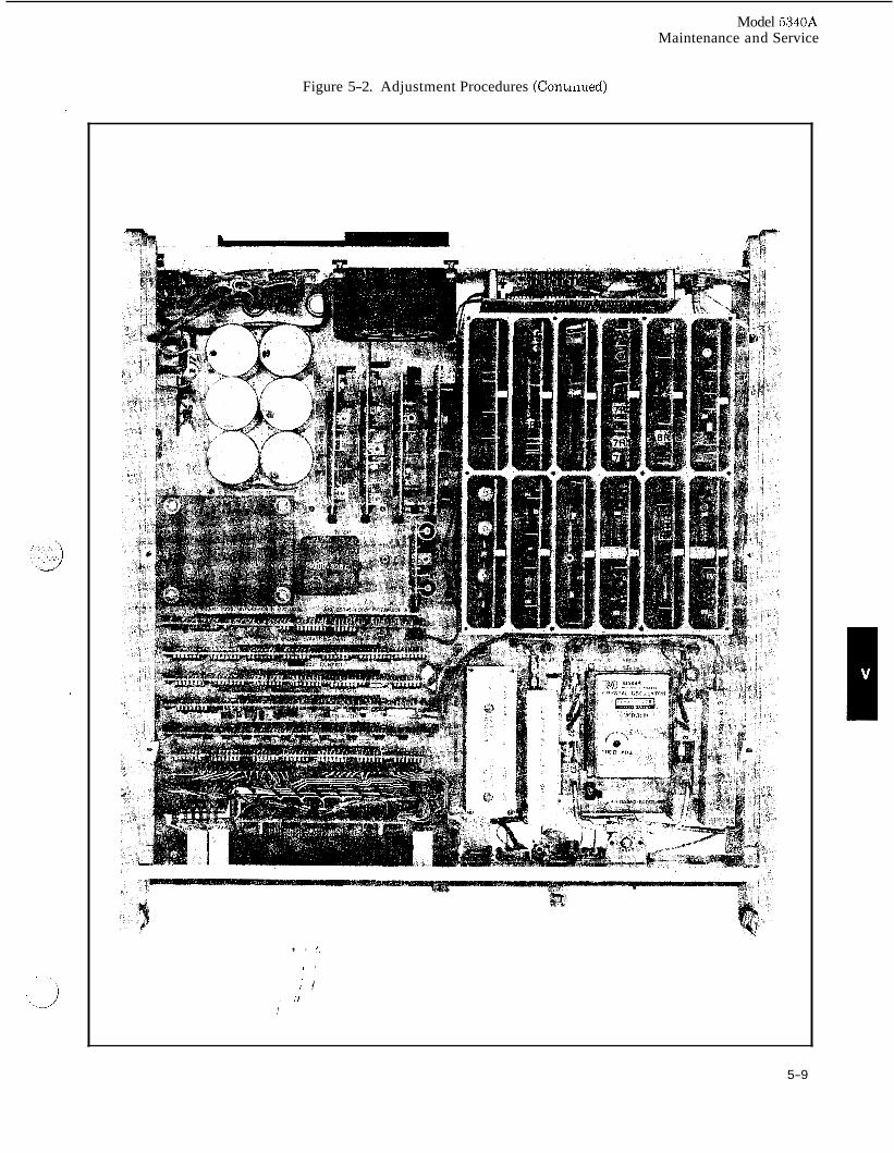
Model 5340A Maintenance and Service
Figure 5-2. Adjustment Procedures (ConLlaued)
, , ,, I '
5-9
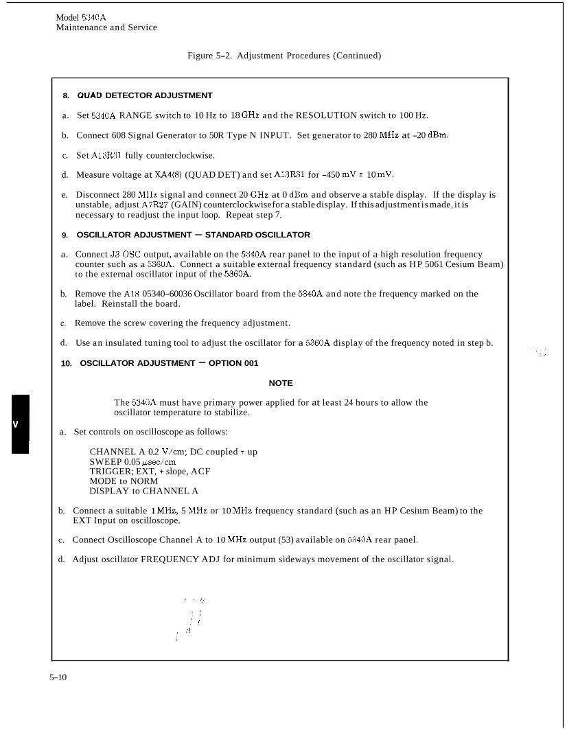
Model 5340A Maintenance and Service
Figure 5-2. Adjustment Procedures (Continued)
8. QUAD DETECTOR ADJUSTMENT
a. Set 5340A RANGE switch to 10 Hz to 18 GHz and the RESOLUTION switch to 100 Hz.
b. Connect 608 Signal Generator to 50R Type N INPUT. Set generator to 280 MHz at -20 dBm.
c. Set A13R31 fully counterclockwise.
d. Measure voltage at XA4(8) (QUAD DET) and set A13R31 for -450 mV f 10 mV.
e. Disconnect 280 MHz signal and connect 20 GHz at 0 dBm and observe a stable display. If the display is unstable, adjust A7R27 (GAIN) counterclockwise for a stable display. If this adjustment is made, it is necessary to readjust the input loop. Repeat step 7.
9. OSCILLATOR ADJUSTMENT - STANDARD OSCILLATOR
a. Connect 53 OSC output, available on the 5340A rear panel to the input of a high resolution frequency counter such as a 5360A. Connect a suitable external frequency standard (such as HP 5061 Cesium Beam) to the external oscillator input of the 5360A.
b. Remove the A18 05340-60036 Oscillator board from the 5340A and note the frequency marked on the label. Reinstall the board.
Remove the screw covering the frequency adjustment.
Use an insulated tuning tool to adjust the oscillator for a 5360A display of the frequency noted in step b.
c.
d.
10. OSCILLATOR ADJUSTMENT - OPTION 001
NOTE
The 5340A must have primary power applied for at least 24 hours to allow the oscillator temperature to stabilize.
a. Set controls on oscilloscope as follows:
CHANNEL A 0.2 V/cm; DC coupled + up SWEEP 0.05 psec/cm TRIGGER; EXT, + slope, ACF MODE to NORM DISPLAY to CHANNEL A
b. Connect a suitable 1 MHz, 5 MHz or 10 MHz frequency standard (such as an HP Cesium Beam) to the EXT Input on oscilloscope.
c. Connect Oscilloscope Channel A to 10 MHz output (53) available on 5340A rear panel.
d. Adjust oscillator FREQUENCY ADJ for minimum sideways movement of the oscillator signal.
5-10
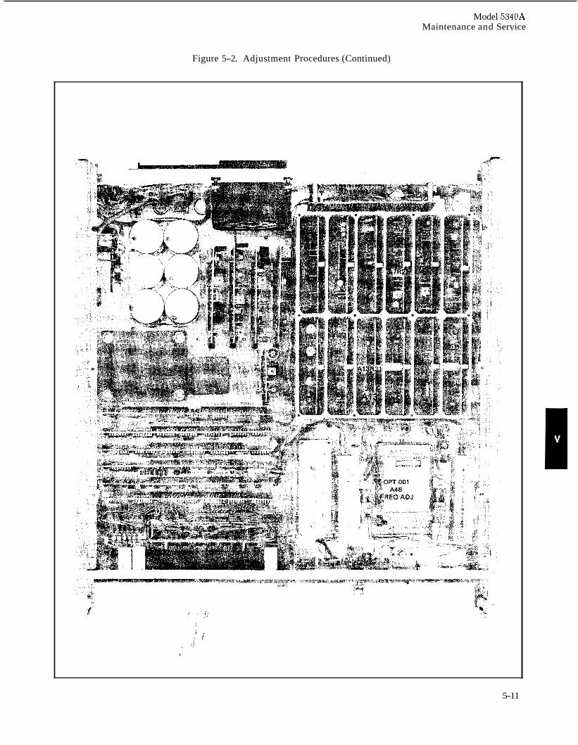
Model 5340A Maintenance and Service
Figure 5-2. Adjustment Procedures (Continued)
, :J I
5-11
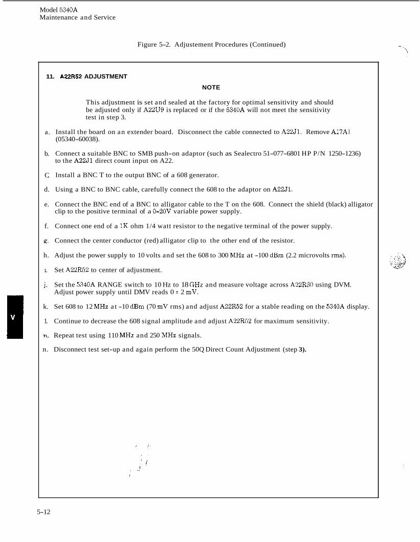
Model 5340A Maintenance and Service
Figure 5-2. Adjustement Procedures (Continued)
11. A22R52 ADJUSTMENT
a.
b.
C.
d.
e.
f.
g.
h.
1.
j.
k.
1.
n.
n.
NOTE
This adjustment is set and sealed at the factory for optimal sensitivity and should be adjusted only if A22U9 is replaced or if the 5340A will not meet the sensitivity test in step 3.
Install the board on an extender board. Disconnect the cable connected to A22J1. Remove A17A1 (05340-60038).
Connect a suitable BNC to SMB push-on adaptor (such as Sealectro 51-077-6801 HP P/N 1250-1236) to the A22J1 direct count input on A22.
Install a BNC T to the output BNC of a 608 generator.
Using a BNC to BNC cable, carefully connect the 608 to the adaptor on A22J1.
Connect the BNC end of a BNC to alligator cable to the T on the 608. Connect the shield (black) alligator clip to the positive terminal of a 0-2OV variable power supply.
Connect one end of a 1K ohm 1/4 watt resistor to the negative terminal of the power supply.
Connect the center conductor (red) alligator clip to the other end of the resistor.
Adjust the power supply to 10 volts and set the 608 to 300 MHz at -100 dBm (2.2 microvolts rms).
Set A22R52 to center of adjustment.
Set the 5340A RANGE switch to 10 Hz to 18 GHz and measure voltage across A22R30 using DVM. Adjust power supply until DMV reads 0 * 2 mV.
Set 608 to 12 MHz a t -10 dBm (70 mV rms) and adjust A22R52 for a stable reading on the 5340A display.
Continue to decrease the 608 signal amplitude and adjust A22R52 for maximum sensitivity.
Repeat test using 110 MHz and 250 MHz signals.
Disconnect test set-up and again perform the 50Q Direct Count Adjustment (step 3).
5-12
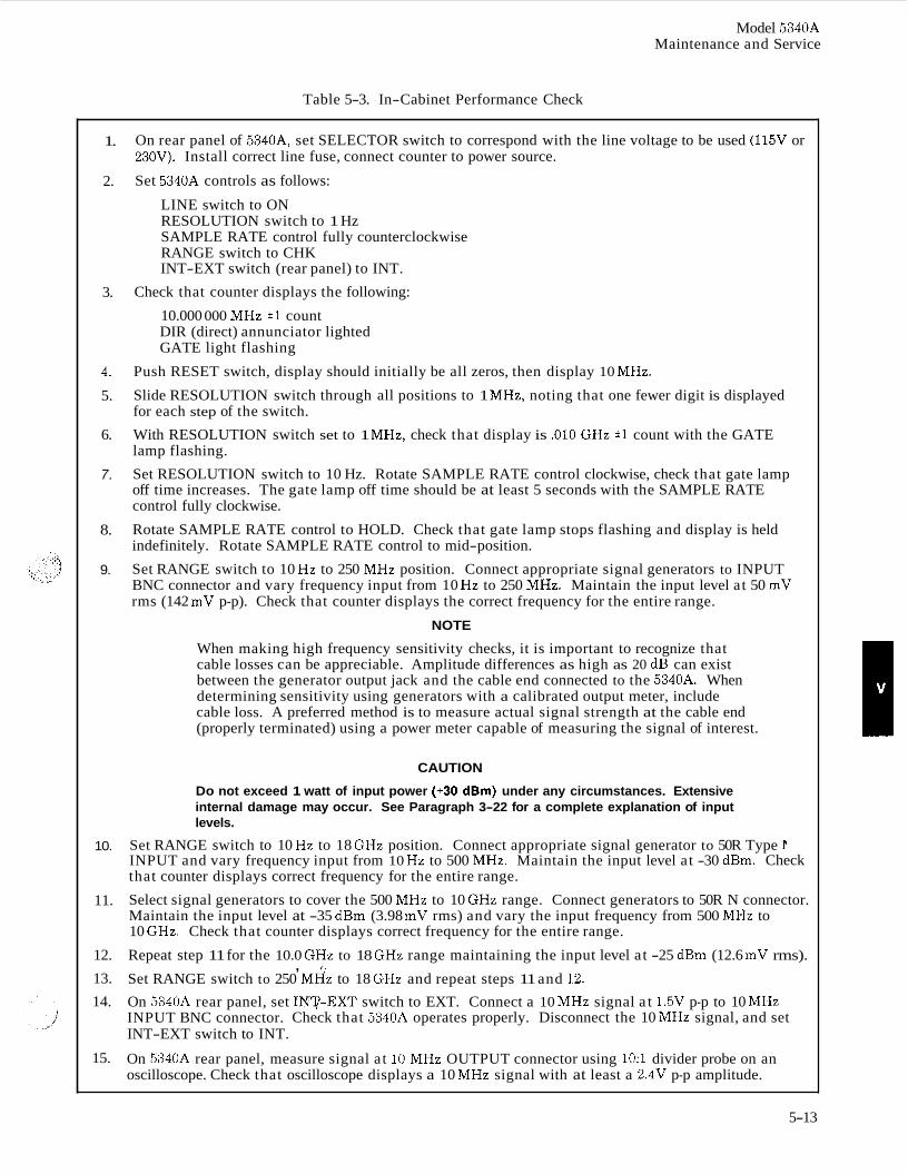
Model 5340A Maintenance and Service
Table 5-3. In-Cabinet Performance Check
1.
2.
3.
4.
5.
6.
7.
8.
9.
10.
11.
12.
13. 14.
15.
On rear panel of 5340A, set SELECTOR switch to correspond with the line voltage to be used (115V or 230V). Install correct line fuse, connect counter to power source.
Set 5340A controls as follows:
LINE switch to ON RESOLUTION switch to 1 Hz SAMPLE RATE control fully counterclockwise RANGE switch to CHK INT-EXT switch (rear panel) to INT.
Check that counter displays the following:
10.000 000 MHz *l count DIR (direct) annunciator lighted GATE light flashing
Push RESET switch, display should initially be all zeros, then display 10 MHz.
Slide RESOLUTION switch through all positions to 1 MHz, noting that one fewer digit is displayed for each step of the switch.
With RESOLUTION switch set to 1 MHz, check that display is .010 GHz *1 count with the GATE lamp flashing.
Set RESOLUTION switch to 10 Hz. Rotate SAMPLE RATE control clockwise, check that gate lamp off time increases. The gate lamp off time should be at least 5 seconds with the SAMPLE RATE control fully clockwise.
Rotate SAMPLE RATE control to HOLD. Check that gate lamp stops flashing and display is held indefinitely. Rotate SAMPLE RATE control to mid-position.
Set RANGE switch to 10 Hz to 250 MHz position. Connect appropriate signal generators to INPUT BNC connector and vary frequency input from 10 Hz to 250 MHz. Maintain the input level at 50 mV rms (142 mV p-p). Check that counter displays the correct frequency for the entire range.
NOTE
When making high frequency sensitivity checks, it is important to recognize that cable losses can be appreciable. Amplitude differences as high as 20 dB can exist between the generator output jack and the cable end connected to the 5340A. When determining sensitivity using generators with a calibrated output meter, include cable loss. A preferred method is to measure actual signal strength at the cable end (properly terminated) using a power meter capable of measuring the signal of interest.
CAUTION
Do not exceed 1 watt of input power (+30 dBm) under any circumstances. Extensive internal damage may occur. See Paragraph 3-22 for a complete explanation of input levels.
Set RANGE switch to 10 Hz to 18 GHz position. Connect appropriate signal generator to 50R Type P INPUT and vary frequency input from 10 Hz to 500 MHz. Maintain the input level at -30 dBm. Check that counter displays correct frequency for the entire range.
Select signal generators to cover the 500 MHz to 10 GHz range. Connect generators to 50R N connector. Maintain the input level at -35 dBm (3.98 mV rms) and vary the input frequency from 500 MHz to 10 GHz. Check that counter displays correct frequency for the entire range.
Repeat step 11 for the 10.0 GHz to 18 GHz range maintaining the input level at -25 dBm (12.6 mV rms).
Set RANGE switch to 250 MHz to 18 GHz and repeat steps 11 and 12.
On 5340A rear panel, set INY-EXT switch to EXT. Connect a 10 MHz signal a t 1.5V p-p to 10 MHz INPUT BNC connector. Check that 5340A operates properly. Disconnect the 10 MHz signal, and set INT-EXT switch to INT.
On 5340A rear panel, measure signal at 10 MHz OUTPUT connector using 1O:l divider probe on an oscilloscope. Check that oscilloscope displays a 10 MHz signal with at least a 2.4V p-p amplitude.
, I I ,
5-13
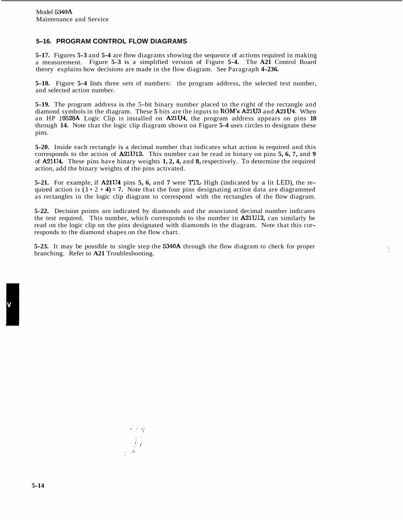
Model 5340A Maintenance and Service
5-16. PROGRAM CONTROL FLOW DIAGRAMS
5-17. Figures 5-3 and 5-4 are flow diagrams showing the sequence of actions required in making a measurement. The A21 Control Board theory explains how decisions are made in the flow diagram. See Paragraph 4-236.
5-18. and selected action number.
Figure 5-3 is a simplified version of Figure 5-4.
Figure 5-4 lists three sets of numbers: the program address, the selected test number,
5-19. The program address is the 5-bit binary number placed to the right of the rectangle and diamond symbols in the diagram. These 5 bits are the inputs to ROM’s A21U3 and A21U4. When an HP 10528A Logic Clip is installed on A21U4, the program address appears on pins 10 through 14. Note that the logic clip diagram shown on Figure 5-4 uses circles to designate these pins.
5-20. Inside each rectangle is a decimal number that indicates what action is required and this corresponds to the action of A21U13. This number can be read in binary on pins 5, 6, 7, and 9 of A21U4. These pins have binary weights 1, 2, 4, and 8, respectively. To determine the required action, add the binary weights of the pins activated.
5-21. For example, if A21U4 pins 5, 6, and 7 were TTL High (indicated by a lit LED), the re- quired action is (1 + 2 + 4) = 7. Note that the four pins designating action data are diagrammed as rectangles in the logic clip diagram to correspond with the rectangles of the flow diagram.
5-22. Decision points are indicated by diamonds and the associated decimal number indicates the test required. This number, which corresponds to the number in A21U12, can similarly be read on the logic clip on the pins designated with diamonds in the diagram. Note that this cor- responds to the diamond shapes on the flow chart.
5-23. It may be possible to single step the 5340A through the flow diagram to check for proper branching. Refer to A21 Troubleshooting.
i
I
5-14
Model 5340A Maintenance and Service
Figure 5-3. Simplified Flow Diagram of 5340A Program Control
RESET
RESET DISPLAY
A . TURNOFF I I vcos z DELAY 10ms
THERE A DIRECT
COUNT
TURN ON VCOS RELEASE STATE COUNTER
SEARCH AND
TRANSFER
LOCKED?
CHECKVALUE
. . 1
1 1
MEASURE FREOUENCYOF SIGNAL
SHIFT DATA INTO DISPLAY
INTO OUTPUT
SAMPLE RATE DELAY T
5-15
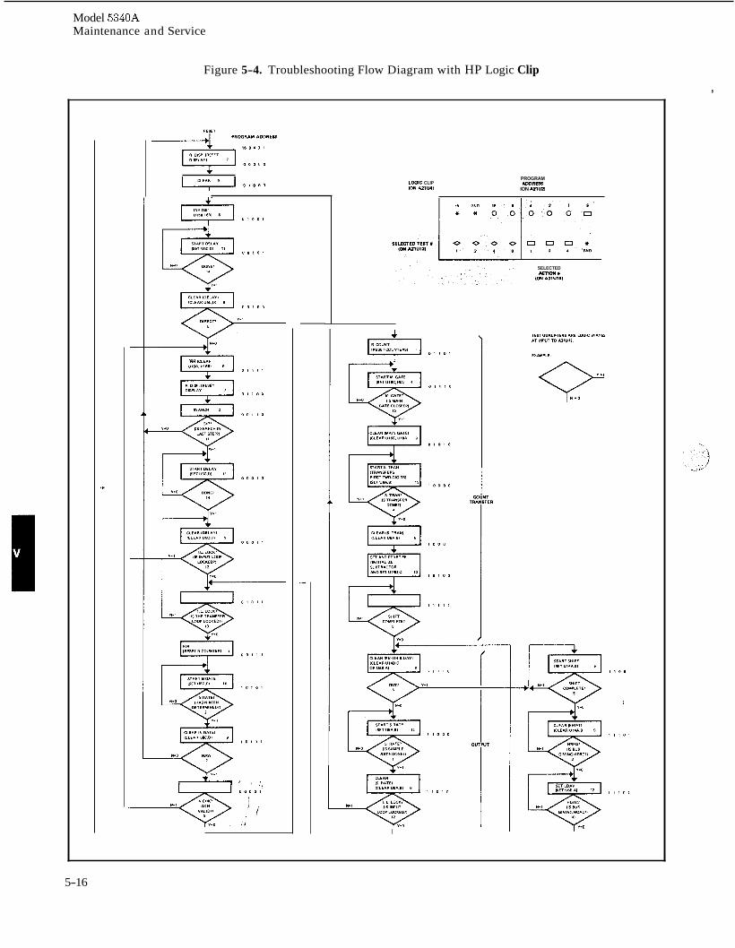
Model 5340A Maintenance and Service
Figure 5-4. Troubleshooting Flow Diagram with HP Logic Clip
1-1 0 , 0 0 0
* ,-, I , I
LOGIC CLIP ION AZlWI
PROGRAM ADDRES
ION A21Ull
SELECTED M I O N I
ION u i u w
I
,
5-16
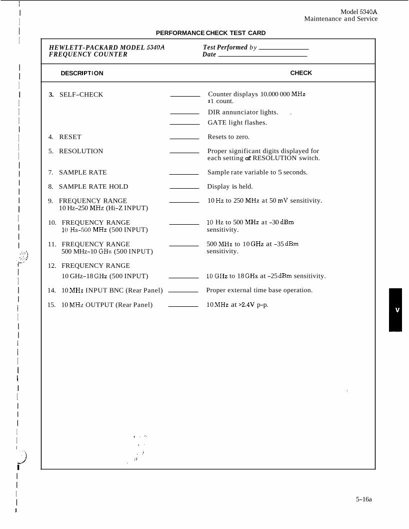
I I I I I
I I I I I I I I I I I I I I I I I I I I I
1- ~ .,J I I I I 1 I I I I I I I I I I I I I I I I
i I I I I I
Model 5340A Maintenance and Service
PERFORMANCE CHECK TEST CARD
HEWLETT-PACKARD MODEL 5340A FREQUENCY COUNTER Date
Test Performed by
CHECK DESCR l PTl ON
3. SELF-CHECK
4. RESET
5. RESOLUTION
7. SAMPLE RATE
8. SAMPLE RATE HOLD
9. FREQUENCY RANGE 10 Hz-250 MHz (Hi-Z INPUT)
10. FREQUENCY RANGE 10 Hz-500 MHz (500 INPUT)
11. FREQUENCY RANGE 500 MHz-10 GHz (500 INPUT)
12. FREQUENCY RANGE 10 GHz-18 GHz (500 INPUT)
14. 10 MHz INPUT BNC (Rear Panel)
15. 10 MHz OUTPUT (Rear Panel)
Counter displays 10.000 000 MHz *1 count.
DIR annunciator lights. .
GATE light flashes.
Resets to zero.
Proper significant digits displayed for each setting of RESOLUTION switch.
Sample rate variable to 5 seconds.
Display is held.
10 Hz to 250 MHz at 50 mV sensitivity.
10 Hz to 500 MHz at -30 dBm sensitivity.
500 MHz to 10 GHz at -35 dBm sensitivity.
10 GHz to 18 GHz at -25 dBm sensitivity.
Proper external time base operation.
10 MHz at >2.4V p-p.
, , r .
I '
5-16a
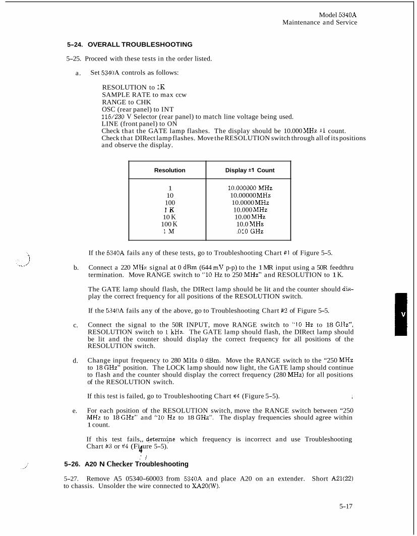
Model 5340A Maintenance and Service
Resolution
1 10 100 1 K
10 K 100 K 1 M
5-24. OVERALL TROUBLESHOOTING
Display *1 Count
10.000000 MHz 10.00000 MHz 10.0000 MHz 10.000 MHz 10.00 MHz 10.0 MHz .010 GHz
5-25. Proceed with these tests in the order listed.
a. Set 5340A controls as follows:
RESOLUTION to 1K SAMPLE RATE to max ccw RANGE to CHK OSC (rear panel) to INT 115/230 V Selector (rear panel) to match line voltage being used. LINE (front panel) to ON Check that the GATE lamp flashes. The display should be 10.000 MHz *1 count. Check that DIRect lamp flashes. Move the RESOLUTION switch through all of its positions and observe the display.
If the 5340A fails any of these tests, go to Troubleshooting Chart #1 of Figure 5-5.
b. Connect a 220 MHz signal at 0 dBm (644 mV p-p) to the 1 MR input using a 50R feedthru termination. Move RANGE switch to “10 Hz to 250 MHz” and RESOLUTION to 1 K.
The GATE lamp should flash, the DIRect lamp should be lit and the counter should dis- play the correct frequency for all positions of the RESOLUTION switch.
If the 5340A fails any of the above, go to Troubleshooting Chart #2 of Figure 5-5.
Connect the signal to the 50R INPUT, move RANGE switch to “10 Hz to 18 GHz”, RESOLUTION switch to 1 kHz. The GATE lamp should flash, the DIRect lamp should be lit and the counter should display the correct frequency for all positions of the RESOLUTION switch.
I c.
d. Change input frequency to 280 MHz 0 dBm. Move the RANGE switch to the “250 MHz to 18 GHz” position. The LOCK lamp should now light, the GATE lamp should continue to flash and the counter should display the correct frequency (280 MHz) for all positions of the RESOLUTION switch.
If this test is failed, go to Troubleshooting Chart #4 (Figure 5-5). i
For each position of the RESOLUTION switch, move the RANGE switch between “250 MHz to 18 GHz” and “10 Hz to 18 GHz”. The display frequencies should agree within 1 count.
If this test fails,, +termi,ne which frequency is incorrect and use Troubleshooting Chart #3 or #4 (Fi ure 5-5).
e.
4 , I
5-26. A20 N Checker Troubleshooting
5-27. Remove A5 05340-60003 from 5340A and place A20 on a n extender. Short A21(22) to chassis. Unsolder the wire connected to XAZO(W).
5-17
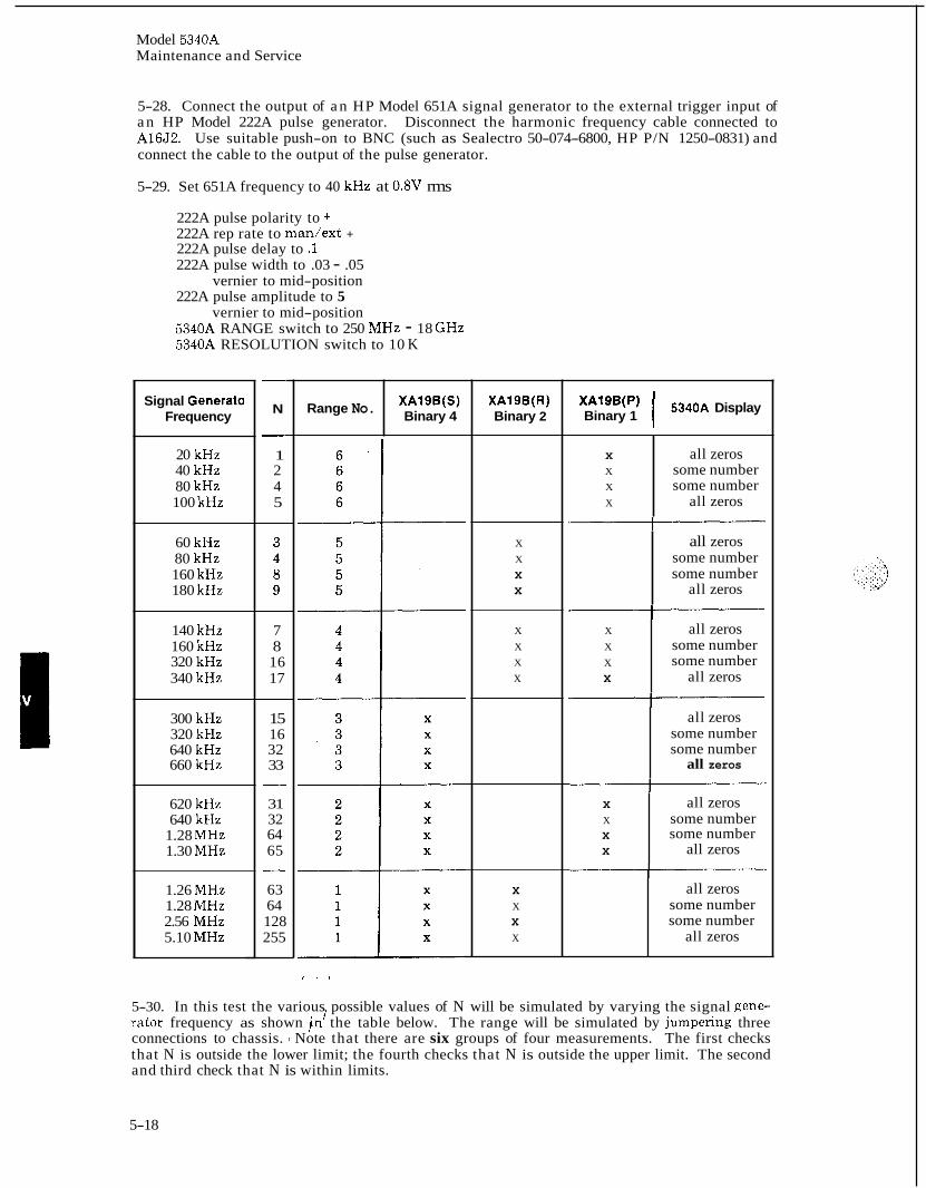
Model 5340A Maintenance and Service
X
X
X
X
5-28. Connect the output of a n HP Model 651A signal generator to the external trigger input of a n HP Model 222A pulse generator. Disconnect the harmonic frequency cable connected to A16J2. Use suitable push-on to BNC (such as Sealectro 50-074-6800, HP P/N 1250-0831) and connect the cable to the output of the pulse generator.
5-29. Set 651A frequency to 40 kHz at 0.8V rms
all zeros some number some number
all zeros
222A pulse polarity to + 222A rep rate to man/ext + 222A pulse delay to .1 222A pulse width to .03 - .05
vernier to mid-position 222A pulse amplitude to 5
vernier to mid-position 5340A RANGE switch to 250 MHz - 18 GHz 5340A RESOLUTION switch to 10 K
X
X
X
X
Signal Generato Frequency
20 kHz 40 kHz 80 kHz 100 kHz
60 kHz 80 kHz 160 kHz 180 kHz
140 kHz 160 kHz 320 kHz 340 kHz
300 kHz 320 kHz 640 kHz 660 kHz
620 kHz 640 kHz
1.28 MHz 1.30 MHz
1.26 MHz 1.28 MHz 2.56 MHz 5.10 MHz
all zeros some number some number
all zeros
- N
- 1 2 4 5
X
X X
X
7 8 16 17
all zeros some number some number
all zeros
15 16 32 33 - 31 32 64 65 - 63 64 128 255
XA19B(S) Binary 4 Range No. XA19B(R)
Binary 2
X
X
X X
X
X X
X
X X X X
XAf9B(P) 1 5340A Display Binary 1
-I all zeros
some number some number
all zeros
-I
I all zeros
some number some number
all zeros
I
1 all zeros
some number some number
all zeros
I ,
5-30. In this test the various possible values of N will be simulated by varying the signal gene- rator frequency as shown Pn the table below. The range will be simulated by jumpenng three connections to chassis. 1 Note that there are six groups of four measurements. The first checks that N is outside the lower limit; the fourth checks that N is outside the upper limit. The second and third check that N is within limits.
I
5-18
Model 5340A Maintenance and Service
J' ._ ~
5-31. There will be two types of test results: The 5340A will display all zeros or it will display some number. For the first and fourth test in each group, the 5340A should display all zeros. The second and third test should cause a number to be displayed, which is approximately N times 150 MHz. The exact value of the display is not important; it is important to note if the display is all zeros or some number.
5-32. To simulate the RANGE setting, connect to chassis pin connections XA19B(S), XA19B(R), XAlSB(P) when designated by an X. These pins, which have binary weights 4, 2, and 1, respec- tively, are positive true. Thus to simulate Range #6, do not short cut Binary 4 and Binary 2.
5-33. If any test fails, first check the action of the range binary to decimal decoder, which should output a TTL Low for the selected range. For example, when XA19B(P) is shorted to chassis (selecting Range #6) the 6 output (pin 7) of the IC should be 'M'L Low. All others should be TTL High. The decoder is U27 on A20 05340-60018 and U28 on A20 05340-60067. If the first test in a group fails, check the action of the lower limit comparators. This is U19 and U20 on both 05340-60018 and 05340-60067. If the fourth test fails, check the action of the upper limit com- parators (U25 and U26 on 05340-60018 and U26 and U27 on 05340-60067). If the second or third test fails, check both sets. These can easily be tested using a logic comparator.
5-34. Check also the output of the binary N counters for agreement with the value of N listed in the table. This is U12 and U21 on 05340-60018 and U6 and U7 on 05340-60067. Check also the associated inverters.
5-35. A21 Troubleshooting
5-36. Disconnect jumper W2 on A20 and install logic clip on A21 U4. Push front panel RESET pushbutton.
5-37. Use HP 105261' Pulser on A21U2(9) and step through the program. Check for proper branching per Figure 5-4. If the program address will not increment, (locked in a loop) deter- mine from Figure 5-4 which test or action is not being completed. Then check A21U12 or U13 to verify that proper selection is taking place there. If that is OK, trace the circuit to find the cause of the failure.
5-38. If incorrect branching is occurring, a test is giving incorrect results or the A21 circuitry is interpreting it incorrectly. Check the input of A21U12 for proper test logic levels, as noted in Figure 5-4. I
i
5-19
Model 5340A Maintenance and Service
5-39. Power Supply Troubleshooting
a. Determine which power supplies are regulating at an incorrect voltage by measuring the output voltage.
If any supply is a t or near zero volts, the supply could be current limiting. Disconnect the output leads for that supply at the A30 power supply motherboard.
Again measure the voltage. If the output is still bad, the failure exists in the power supply circuit. Use the typical voltage charts shown to isolate the defective components.
If the output obtained in step 3 is now good, there could be a short circuit in the instru- ment, or the supply could be current-limiting improperly. Substitute a resistive load for the supply under test as listed on the next page.
If the output is still good, an excessive load exists somewhere in the instrument. Connect an ohmmeter between ground and on the feeder line in question (which is still discon- nected from its power supply). Start removing the plug-in PC boards until a significant change is observed on the ohmmeter. Then isolate the execessive load. Check also for shorted wires.
If the output obtained in step 4 is bad, the power supply is not able to provide the neces- sary current. Use the typical voltage charts to isolate to the defective component. Look especially for the same voltage on any two leads of a transistor, indicating a shorted transistor.
b.
c.
d.
e.
f.
5-20
REPLACICABLEORTII \CE RECONNECT S l G l l l L &NO OSCILLATOR SIGNAL BACK THROUGH A18
TRACE THROUGH 13
I RTPLACC A22W
I 1 MEASURE LOGIC L l V E L AT A22WllZl REFLACS CABLE MEASURE SIGNAL 1TAZu31141 SHOULO 81 EECL LOW I-O.BVI F R W A J T O A Z S H W L D B E IOMHzATBmmYps
MElLURI LOGIC LEVEL ATA12U3I11 TRACE THROUGH GATING XA22IE1 SHOULO BE TTL A11"B SHOULD Be FECL HIGH lWl CIRCUITSAZZU6. ETC MEASURt LOGLCLEWLAT R E P U C E
ion W01"I
CHECK LOGIC L E V l L AT XAZllJI. REPLACE U3 W O U L D B ~ ~ L H I ~ ~ - W FIX oz -a
FIX m-os MEWRE FOR nr LOG~C LEVELS SHOWN BELOW ClRCUlTRl
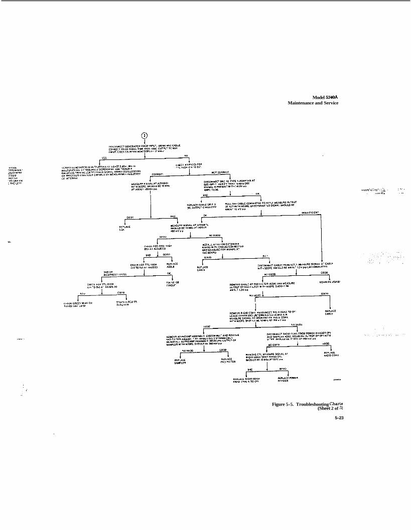
Model 5340A Maintenance and Service
. . . . ..:... *'..j... :..::...', . : :.: .. . .... :I; . ... . .....
Figure 5-5. Troubleshooting Charts (Sheet 2 of 3)
5-23
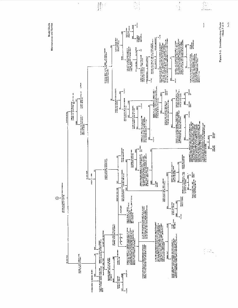
f
3
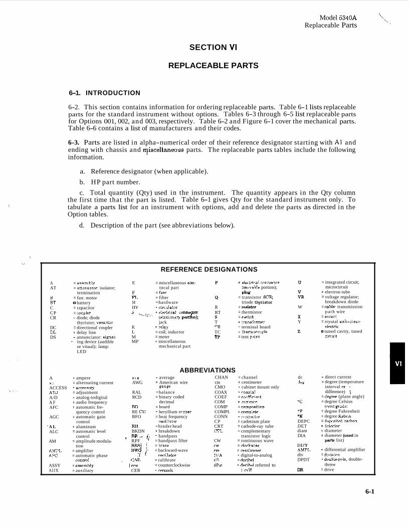
L. Model 5340A Replaceable Parts
SECTION VI
REPLACEABLE PARTS
6-1. INTRODUCTION
6-2. This section contains information for ordering replaceable parts. Table 6-1 lists replaceable parts for the standard instrument without options. Tables 6-3 through 6-5 list replaceable parts for Options 001, 002, and 003, respectively. Table 6-2 and Figure 6-1 cover the mechanical parts. Table 6-6 contains a list of manufacturers and their codes.
6-3. Parts are listed in alpha-numerical order of their reference designator starting with A1 and ending with chassis and Tiscellaneous parts. The replaceable parts tables include the following information.
a. Reference designator (when applicable). b. HP part number. c. Total quantity (Qty) used in the instrument. The quantity appears in the Qty column
the first time that the part is listed. Table 6-1 gives Qty for the standard instrument only. To tabulate a parts list for an instrument with options, add and delete the parts as directed in the Option tables.
d. Description of the part (see abbreviations below).
I
A = aauemhly AT = attenuator; isolator;
B = fan: motor BT battery C = rapacitor CP = roupler CR = diode; diode
thyristor; varactor DC = directional coupler DL = delay line DS = annunciator: signal-
termination
-' ing device (audible or visual); lamp: LED
A a r ACCESS AD.J A/D A F AFC
AGC
' A L ALC
AM
AMPI, APC
= ampere = alternating current = arceuuory = adjustment = analog-todigital = audio frequency = automatic fre-
quency control = automatic gain
control = aluminum = automatic level
control = amplitude modula-
tion = amplifier = automatic phase
E
F FL H HY .i ':
K L M MP
avg AWG
RAL RCD
RD RE CU BFO
un BKDN
RPF t RP ' 8 /[
REFERENCE DESIGNATIONS
= miscellaneous elec-
= fuue = filter =hardware = rirculator =el&rical conn tor
(Rtationary p o 2 n ) ; jack
= relay = coil; inductor = meter = miscellaneous
tncal part
mechanical part
P
9
R RT S T TB TC TP
= rlectriral connedor (movahle portion); Plug
= transistor 8 C R triode thyristor
= reuiutor = thermistor = awitrh = tranufnrmer = terminal hoard =thermocouple = tent point
ABBREVIATIONS = average CHAN = channel = American wire cm = centimeter
=balance COAX = roaxial = binary coded COEF = roefficient
decimal COM =common = board COMP = rompnuition = heryllium copper COMPI. = rnmplete = beat frequency CONN =ronn&r
oacillator CP = cadmium plate =hinder head CRT = cathode-ray tube = hreakdown CTL = complementary = handpass transistor logic = handpass filter CW = rontinuous wave = hraau rw = rlockwiue = backward-wave m = rentimeter
oacillator D/A = digital-to-analog = ralihrate dR = decihel = counterclockwise dRm = dwihnl referred to = reramic I mW
gauge CMO = cabinet mount only
rnntrol ' L , c d ASSY = auuemhly 1 rrw AIJX = auxiliary CER
U
V VR
W
X Y
z
dc deg
"C
O F
OK DEPC DET diam DIA
DIFF AMPI, div DPDT
DR
= integrated circuit; microcircuit
= electron tube = voltage regulator;
breakdown diode = rable; transmission
p a t h wire = uncket = rryutal unit-piezo-
tuned cavity, tuned dRctric
cirruit
= direct current = degree (temperature
interval or r
difference) 1 = degrw (plane angle) = degree Celsius
(rentigrade) = degree Fahrenheit = degree Kelvin = depnuited carhon = detpctor = diameter = diameter (used in
pa- list)
= differential amplifier = diviRion = douhle-pole, double-
thrnw = drive
6-1
Model 5340A Replaceable Parts
ABBREVIATIONS DSR DTI. DVM
EMF EDP
EIXCT ENCAP EXT F FET
F/F FH F11. H FM
FP FREQ F X D Y GI? GH7 G I , GNI) H h HET HEX HD HDW HF HQ HI HP HPF HK
HV H7 IC IT) IF
TMPG in INC D TNCI, TNP INS INT
kH7 k U kV Ih l>P
LED L F I G I,H I JM J J N
hn LK WASH LO LOG
log I.PF I >V m mA MAX MQ MEG
m.
k g
= douhle uidehand = diode transistor logic = digital voltmeter = emitter coupled logic = elertrnmotive force = elertronic data
proresuing = electrolytic = enrapuulated = external = farad = field-effect tran.
uistor = flip-flop = flat head = fillinter head = frequency modula-
= front panel = frequency = fixPd = gram = germanium = figahertz = glaus = ground(ed) =henry = hour =heterodyne =hexagonal =head =hardware =high frequency = merrury =high = Hewlett-Packard =high pauu filter = hour (wed in parts
list) =high voltage = Hertz = integrated circuit = inuide diameter = intermediate fre-
= impregnated = inch = incandement = inrlude(n) = input = inuulation = internal = kilogram =kilohertz = kilohm =kilovolt = pnund = inductance-
rapacitance light-emitting diode
= low frequency = long = left hand = limit = linear taper (used in
= linear
= lork wauher = low: local oucillator = logarithmir taper
( U R ~ in parts list) = logarithm(ir) = low pauti filter = low voltage = meter (distance) = milliampere = maximum = megohm = meg (10s) (used in
tion
qurncy
parta list)
parts list) MET F1.M = metal film MET OX = metal oxide MF = medium frequency;
mirrofarad (used in uartu liut)
MFR
MHz mH mho MIN min
MINAT mm MOD MOM MOS
mu MTG MTR
mV mVar mVdr mVpk
mg
mV P-P
mVrms mW MlJX MY PA PF WH pmho us PV pVnr pVdr pVpk MVP-P
pvrmu PW nA NC N/C NE NEG n F N1 PI, N/O NOM NORM NPN
NPO
NRFR
NSR
ns nW OBD OD OH O P AMPL OPT OSC OX oz R P
PAM
PC PCM I * ,<
PDM 1 p F , !I PHI RRZ PHI, PIN
= manufacturer = milligram = megahertz = millihenry = mho = minimum = minute (time) = minute (plane angle) =miniature = millimeter = modulator = momentary = metal-nxide semi-
mndudnr = millisecond = mounting = meter (indicating
device) = millivolt = millivolt, ac = millivolt, dc = millivolt, peak = millivolt, peak-*
= millivolt, rms = milliwatt = multiplex = mylar = mirrnampere = microfarad = mirrohenry = mirromhn = mirrnsemnd = microvolt = mirrovolt, ac = mirrovolt, dc = micrnvolt, peak = mirrovolt, peak-to-
= micrnvolt, rms = microwatt = nanoampere = no connection = normally closed = neon = negative = nanofarad = nickel plate = normally open = nominal = normal = negative-positive
negative = negative-positive
zero (zero tempera- ture coefficient)
= not recommended for field replacement
= not ueparately replaceahle
= nanouecond = nanowatt
order hy description = outside diameter = oval head = operational amplifier = option = oucillator = oxide = ounce = ohm = peak (used in parts
liut) = pulseamplitude
modulation = printed circuit i; pulswode modula- ''tion; pulse-count ; modulation = puluedutation
modulation = pirofarad = phouphor hrnnze = Phillipu = positive-instrinsic-
peak
peak
negative
PIV = peak inverse voltage pk = peak PI, = phase lock PIX) 7 phaee lock oscillator PM = phaRe modulation PNP = pouitivenegative
P /O = part of POLY = polystyrene PORC = porrelain POS = pouitive; position(s)
POSN = position POT = potentiometer P-P = peak-*peak PP = peakb-peak (used
in parts list) PPM = pulue-position
modulation PREAMPI. = preamplifier PRF = pulse-repetition
PRR = pulse repetition rate DR '' = picosecond
pouitive
(uued in parts list)
fwquency
tir PTM
PWM
PWV RC
RECT REF REG REPL RF RFI
RH
RLC
RMO
RND ROM R&P RWV
S
T m U
8
S-R
SCR
SE SECT
= point = pulue-time mndula-
tinn = pulse-width
modulation = peak working voltage = reuiutance
= rectifier = reference = regulated = replaceahle = radio frequency = radio frequency
= round head; right
= resistance-
capacitance
interference
hand
inductance capacitance
= rack mount only = root-mean-square = round = read-only memory = rack and panel = reverwe working
= mattering parameter = secnnd (time) = uecnnd (plane angle) = ulow-hlow (fuse)
(used in parta list) = silicon controlled
rectifier; screw = uelenium = uwtinns
voltage
SEMICON = uemiconductor SHF = superhigh fre-
quency SI = silicon SIL = uilver SL = slide SNR = uignal-bnoise ratio SPDT = uingle-pole, double
throw SPG =upring SR = uplit ring SPST = singlepole. single-
throw SSB = single sidehand SST = stainless steel STL = uteel SQ = square SWR = ntanding-wave ratio SYNC synchronize T = timed (slow-blow
TA = tantalum TC =temperature
TD = time delay TERM =terminal
fuse)
rompensating
TIT TGI, THD THRU TT TOJ, TRIM TSTR TTI,
TV TVJ TWT U
lJF
IJHF IJNREG V VA Var VAR VCO
Vdc VDCW
V(F) VFO
VHF Vpk V P P Vrmu VSWR
VTO
VTVM
V(X) W W/ WTV
ww w/o YIG zo
= thin-film transistor = toggle =thread =through = titanium = tolerance = trimmer = tranuistnr = tranuistor-transistor
= television = television interference = traveling wave tube = micro (used
in parts list) = microfarad (used in
pa& list) = ultrahigh frequency = unregulated = volt = voltampere = volta, ac = variahle = voltagecontrnlled
= voltn, dc voltu, dc, working (used in parts list)
= voltn, filtered = variahle-frequency
oscillator = very-high frequency = voltn, peak = voltu, peak-to-peak = volts, rms = voltage standing
wave ratio = voltage-tuned
oRcillator = vacuum-tuhe
voltmeter = voltn, uwitched =wat t = with = working inverse
voltage = wirewound = without = yttrium-iron-garnet = characteristic
impedance
logir
oucillatnr
NOTE All abbreviationu in the parts list will be in upper case.
MULTlPLlERSi
Abbreviation Prellx Multiple
T tera 1012 G giga 109 M mega 10" k kiln 108 da deka 10 d deci 10-1
centi 10-2 m milli 1 0 - 3 c1 micro 10-6 n nann P pico 1W'Z f femto 10-16
a atto in-
C
6-2
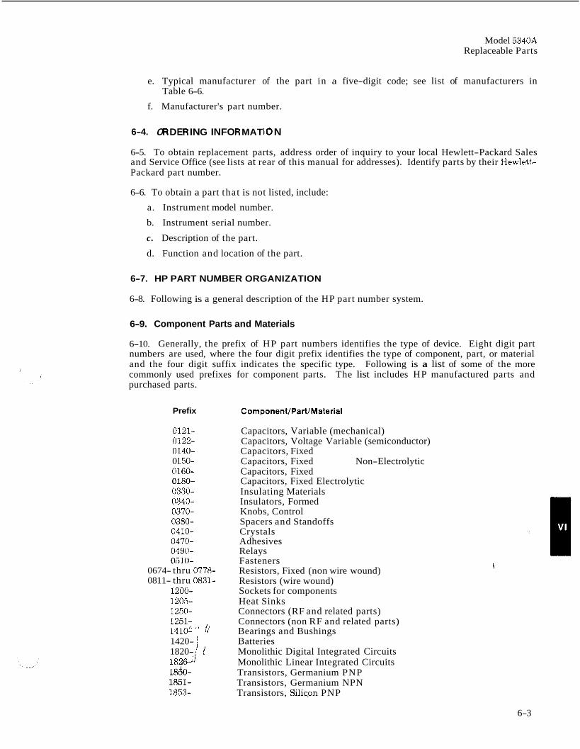
Model 5340A Replaceable Parts
e. Typical manufacturer of the part in a five-digit code; see list of manufacturers in Table 6-6.
f. Manufacturer's part number.
6-4. 0 R D E R I N G INFO R MAT I0 N
6-5. To obtain replacement parts, address order of inquiry to your local Hewlett-Packard Sales and Service Office (see lists at rear of this manual for addresses). Identify parts by their Hewlett- Packard part number.
6-6. To obtain a part that is not listed, include:
a. Instrument model number.
b. Instrument serial number.
c. Description of the part.
d. Function and location of the part.
6-7. HP PART NUMBER ORGANIZATION
6-8. Following is a general description of the HP part number system.
6-9. Component Parts and Materials
6-10. Generally, the prefix of HP part numbers identifies the type of device. Eight digit part numbers are used, where the four digit prefix identifies the type of component, part, or material and the four digit suffix indicates the specific type. Following is a list of some of the more commonly used prefixes for component parts. The list includes HP manufactured parts and purchased parts.
Prefix
0121- 0122- 0140- 0 150- 0160- 0180- 0330- 0340- 0370- 0380- 0410- 0470- 0490- 0510-
0674- thru 0778- 0811- thru 0831-
1200- 1205- 1250- 1251- 14101- " il 1420- 1 I 1820- i 1826~') 18hO- 1851- 1853-
ComponenVParVMaterial
Capacitors, Variable (mechanical) Capacitors, Voltage Variable (semiconductor) Capacitors, Fixed Capacitors, Fixed Non-Electrolytic Capacitors, Fixed Capacitors, Fixed Electrolytic Insulating Materials Insulators, Formed Knobs, Control Spacers and Standoffs Crystals Adhesives Relays Fasteners Resistors, Fixed (non wire wound) Resistors (wire wound) Sockets for components Heat Sinks Connectors (RF and related parts) Connectors (non RF and related parts) Bearings and Bushings Batteries Monolithic Digital Integrated Circuits Monolithic Linear Integrated Circuits Transistors, Germanium PNP Transistors, Germanium NPN Transistors, Silicpn PNP
6-3
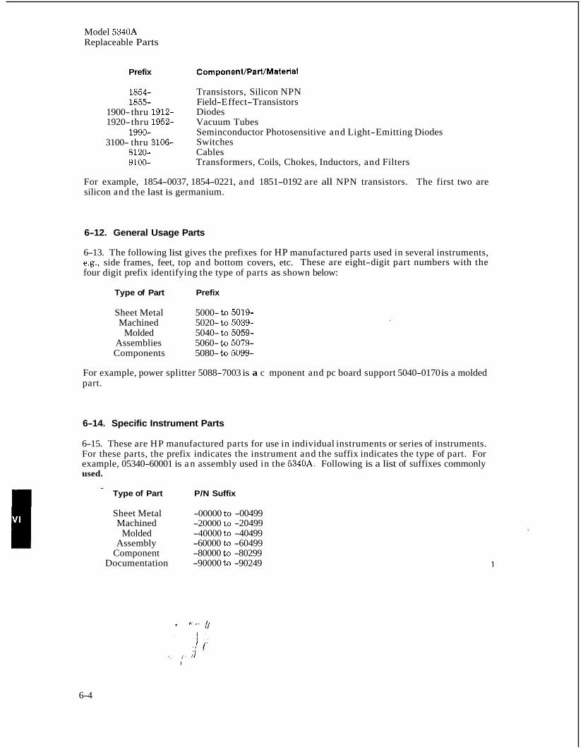
Model 5340A Replaceable Parts
Prefix Component/Part/MateriaI
1854- 1855-
1900- thru 1912- 1920- thru 1952-
1990- 3100- thru 3106-
8120- 9100-
Transistors, Silicon NPN Field-E ffect-Transistors Diodes Vacuum Tubes Seminconductor Photosensitive and Light-Emitting Diodes Switches Cables Transformers, Coils, Chokes, Inductors, and Filters
For example, 1854-0037, 1854-0221, and 1851-0192 are all NPN transistors. The first two are silicon and the last is germanium.
6-12. General Usage Parts
6-13. The following list gives the prefixes for HP manufactured parts used in several instruments, e.g., side frames, feet, top and bottom covers, etc. These are eight-digit part numbers with the four digit prefix identifying the type of parts as shown below:
Type of Part Prefix
Sheet Metal 5000- to 5019- Machined 5020- to 5039-
Molded 5040- to 5059- Assemblies 5060- to 5079- Components 5080- to 5099-
For example, power splitter 5088-7003 is a c part.
6-14. Specific Instrument Parts
mponent and pc board support 5040-0170 is a molded
6-15. These are HP manufactured parts for use in individual instruments or series of instruments. For these parts, the prefix indicates the instrument and the suffix indicates the type of part. For example, 05340-60001 is a n assembly used in the 5340A. Following is a list of suffixes commonly used.
- Type of Part P/N Suffix
Sheet Metal -00000 to -00499 Machined -20000 to -20499
Molded -40000 to -40499 Assembly -60000 to -60499
Component -80000 to -80299 Documentation -90000 to -90249
6-4
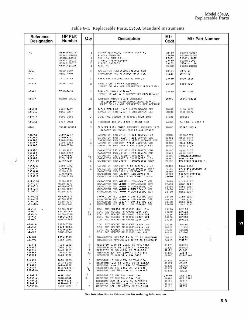
Model 5340A Replaceable Parts
Table 6-1. Replaceable Parts, 5340A Standard Instruments
Reference Designation
A 1
A l C 1 A1C2
A 1 R l
A l A l *
A lA2*
A1631
AlA3C1 AlA3C2
A l A 3 L l
AlA3R1
A l A 4
A lb4C1 A144C2 AlA4C3 AlA4C4 AlA4CS
AlA4Cb AlA4C7 AlA4C8 A164C9 A 1A4C 10
A 1A4C11 A U K 1 2 A l A k C l 3 A l A 4 C l 4 A 1 A 4C15
A 1 A 4C 1 6 AlA4C 1 7 LlA4C.18 AlA4C19 AlA4CZO
A lA4CZ l A 1 A 4C 22 A144C23 LlA4C24
A l A 4 . 1 - AlA4LZ AlA4L3 A lB4L4 AlA4L5
A lA4Lb AlA4L7 A144L8 AlA4L9
AlA4Q1 AlA402
AlA4R1 A l A W 2 AlA4R3 AlA4R4 ~ 1 ~ 4 ~ 5
AlA4R6 PlL4R7
LlA4R9 L 1 P4R 1 0
4 l A 4 R l l 41641112 LIA4R13 41A4R14 2 lA4R 15
PIA~RB
HP Part Number
053GO-6U017 05340 00009 05340-00012 05340 00017 05340-00019 C 534C-2'.C33
0160 0204 0160- 0204
l 8 l U 0118
5088 7004
c c, 8 8- 711 35
05340-60042
C 1611-3277 0160 3277
9100-2256
0757-0963
05340 65014
G 160-32 77 0160-3277 0 160-22 3 8 0160-3284 0 160- 30 28
01bO-32 77 C 160-3277
0160-2198 0140-5224
0 160-21 50 0140-02 17 0160- 21 50 0180-0197 0 160-2198
0160-3277 0 160-3277 0160-3277 0 160-3277 0 160-3277
0 160-32 77 0 160-3277 0 160-3277 0 160-2743
9 100-2247 9100-2265 9 100-0368 9100-0368 9100-2265
9100-0368 9100-0368 9100-C368 9 100-2247
1854-0345 1854- 0345
1698-6242 0698 5182 3698-3374 3698- 51 74 3698-3380
>698 6283 1698-5 178 1698-5181 1698-3374 1698- 81 28
1698 3380 1 69 8- 33 80 )698-8128 1698-8128 ' 1698-5426
0180-0197
QtY
1 I 3 3 2 1
5
1
2
2
1
85
2
1
1
1 1 1
32 2 1
2 1
1
7 I1 11
6
2 2 4
11 3
1 1
I f '$
i , 2 -
Description
B C P Q I ) ASSFHRLYv PREAHFLIFlER Y 1 PLATL. SAUPLER SHIF. LO e S I M P L E R CCVEP. PHFAMPLIFIER PLATE. S A U P L E R HOUS I N 6
CAPACITOR-FXO 55OOPF2OOWVOC C C R CAPACITOP-FXC ~ ~ ~ ~ u P F Z L ~ W V O C CER
TFRMINATI0k:COAX S Y A S O OHU 1 W
THIN FILM SbPPLER ASSEMBLY *PART OF A 1 1 NOT SEPARATELY FEPLACEARLk
SAHPLFR DRIVF ASStMBLY *PART OF A l , NflT SEPAPATELY PFPLACLABLE
SAMPLER WTPUT BOARD ASSEMBLY (LOAOEO ON 05340 20042 BLANK ROAPlJ1
*PART OF A 1 t NOT SEPAPATELY REPLACEABLF
CAPACITCIP-FXI? - '1UF +-20% SOWVDC CFR CIPACITOR-FXO -01UF +-20% SOWVCC CER
COIL FXO MOLOEO RF CHOKE .56UH 10%
RESISTOR 43K 2% .125W F TC=O+ 100
PREAHPLIFIEk BOARD ASSEMBLY (SERIES 1220 (LOAOFO ON 05340- 20014 BLANK 8ClAPOI
CAPACITOP-FXO .0llJF +-2OX 50WVOC C C R CAPACITOR FXO -01UF + 202 SOWVOC CES CAPACITOR FXO 1.5PF + .25PF SOOWVDC CER CAPACITOR-FXO 22PF + - lo% l O O W V O C CER CAPACITOR FXO 10PF + l iJ% lOOUVOC CER
CAPACITOR FXD .OlUF + 2 0 1 5OWVDC CER CAPACITOR FXO .OlUF + 20Z 50WVOC CEP CAPACITPR FXD: Z.ZUF+ 10% Z O V O C TA CAPACITOR FXO ZOPF + 5% 3OOUVCC UlCA CAPRCITOR FXO 280PF + 1% 300WVOC UICA
CAPACITOR FXD 33PF + 5'11 300WVOC M I C A CAPACITOR FXO 140PF + 21 3DOWVDC M I C A CAPACITCR FXO 33PF + 5 Z 300WVDC UICA CAPLCITOR FXO: 2.2UF+ 1OX ZOVDC 74 CAPACITOR FXD 2DPF + 5 % 300WVOC M I C A
CAPACITCR FXO .OlUF + 20% 5OWVDC CER CAPACITOR FXO -0 lUF + 20% SOWVOC CER CAPACITOR FXO -01UF + 20% SOWVOC CFR CAPACITOR FXD .01UF + 2OL SOUVCC CER CAPACITOR. FXO -01UF + 20% SOWVOC CER
CAPLCITOR, FXO .OlUF + ZDI 5OWVOC CER CAPACITOR FXO -01UF t 20% 50WVOC CER CAPACITOR FXO 4 1 U F + 202 5OYVDC C'ER CAPACITOR FXD 33PF + 10% ZOOWVDC CER
COIL FXO UCLOED RF CHOKE .lUH 10% COIL FXO MOLDED RF CHOKE lOUH 1UZ COIL FXD MOLOEO RF CHOKE .33UH l O I I COIL FXO MOLDED RF CHOKE .33UH 10X COIL FXO MOLDED RF CHOKE lOUH 10%
COIL FXO' MOLDED RF CUOKF .33UH 10f COIL FXD MOLDED RF CHOKE -33UH 19% COIL FXO UOLOEO RF CHOKE .33UH 10% COIL FXO MDLOEO RF CHOKF .1UH 10Z
TRANSISTOR NPN 2N5179 S I TO 72 PD=200HU TRANSISTOR NPN 2N5179 SI 10-72 PO=ZOOMW
i iES ISTO(r 1.2K 5 1 .125W CC TC=.+882 RESISTOR 3.SK 5% .125H C C TC=O+R82 RESISTOF. 20 5% .125W CC Ti=0+588 RESISTOR 200 5% -125W CC TC=0+88Z RESISTCR 7 5 OHM 5 Z -12% COMP
RESISTOR 10 5% .125W C C TC=0+588 RESISTOR 1.5K 5L .125W CC TC=O+88Z RESISTOR 3.6K 5 Z -125Y C C TC=O+882 RESISTOR 20 5% .125W CC TC=0+588 RESISTOR 220 5% -125W C C TC=0+882
RESISTOR 7 5 OHU 5% -125Y C3MP RESISTOR 7 5 OHM 5% .125W E J M P RESISTOR 220 5X .125W CC TC=O+882 RESISTOR 220 5% .125W CC TC=0+882 RESISTOR 10K 10% -125U CC TC=O+B82
Mfr Cod€
Z 8 r 6 0 2Y4RO 2 8 4 8 < 20480 2R48O 28480
01121 P1121
2 ~ 8 0
28480
23480
28480
28480 28480
24226
24566
28480
28480 28 48 0 28480 28480 28480
28480 28 48 0 56289 28480 72136
28480 72136 28480 56289 2R4RO
28480 28480 28480 28480 28480
28480 284PO 28480 28490
24226 24 22 6 24226 24226 24226
24226 24226 24226 24226
04713 0471 3
0 1 1 2 1 01121 01121 0 1 12 1 28480
01121 01121 01121 01121 01121
28480 28480 31121 31121 31121 -
Mfr Part Number
05340 60017 05340-00009 C 534"- :0'112 05340 00017 c534'-.,.. 18 05340 20033
SUFR-A2 SMFB-A2
1810 O l l f l
5088 7001
5088- 7005
0160 3277 0160-32 77
101560
C4 118 TO 4302 G
05340 60014
0160 -3277 0160 3277 0160 2238 0160-32fl1 0160 3028
0160 3277 0160 3277 150022SX?02 DL2
DMl5F281F03DOWVIC
0160 2150 OH1 5Fl41GO3OOWV1CE 0160 2150 150D225X902012
0160 2198
0160 2190
0160 3277 0160 3271 0160 3217 0160 3271 0160 3277
D l 6 0 3277 DlbO 3277 31 60 32 77 3140 2743
LO1100 LO/lOZ LO1330 LO1330 L0/102
101330 101330 101330 LO1100
!N5179 !N5179
I61225 I83925 I82005 I82015 b 9 8 - 3 3 8 0
I81 005 161525 183625 ,82005 82215
1698 3380 lb98 3380 82215 82215 81031
See introduction to this section for ordering information
6-5
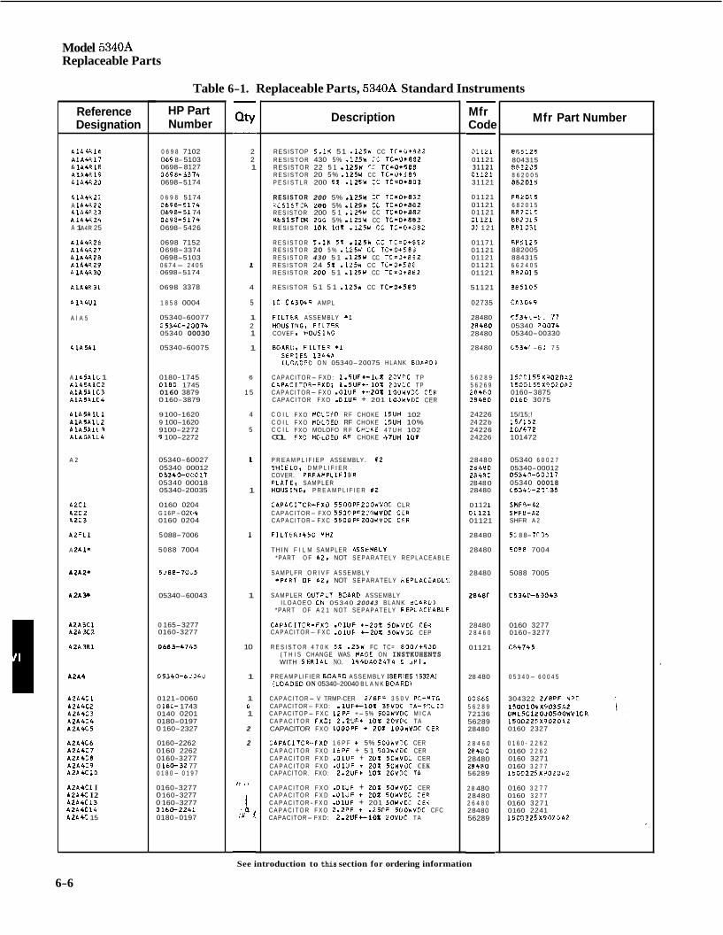
Model 5340A Replaceable Parts
Table 6-1. Replaceable Parts, 5340A Standard Instruments
Reference Designation
A 1 4 4 R 1 6 A l A 4 R 1 7 A l A 4 R l E A l A 4 R 1 9 A l A W 2 0
A l A 4 H 2 1 A 1 A 4 K 2 2 A l A 4 P 2 3 A l A C R 2 4 A 1 A4R 25
A l A 4 R 2 6 A l A 4 R 2 7 A I A 4 R 2 8 A l A 4 4 2 9 P l A 4 R 3 0
A l A 4 R 3 1
A 1 4 4 U 1
A l A 5
A I A 5 A 1
A l A 5 A l C 1 A 1 A 5 A l C Z A 1 A 5 A l C 3 A l A 5 4 1 C 4
A l A 5 6 1 L 1 A l A 5 A l L Z A l A 5 A l L 1 A l A 5 A l L t
A 2
A 2 C 1 A Z C Z azc3
A 2 F L 1
A 2 A I*
A 2 4 2 *
A 2 A 3 *
A 2 A 3 C l A 2 A 3 C 2
A t A 3 R 1
A 2 1 4
A Z A 4 C 1 A 2 A 4 C 2 A Z A 4 C 3 A Z A 4 C 4 A 2 A 4 C 5
A 2 A 4 C 6 A 2 A 4 C 7 A 2 A 4 C 8 A Z A 4 C 9 A 2 A U l O
A 2 A 4 C l I A 2 A U I2 A Z A 4 C 1 3 A 2 A K l 4 A Z i U 15
HP Part Number
0 6 9 8 7102 0 6 5 8- 5103 0698- 8127 0698-3374 0698-5174
0 6 9 8 5174 0 6 9 8 - 5 1 7 4 0 698-51 74 0 6 9 8 - 5 1 7 4 0 698- 5426
0698 7152 0 698-3374 0698-5103 0 6 7 4- 2 4 0 5 0698-5174
0698 3378
1 8 5 8 0004
05340-60077 G 5 3 4 C - 2 0 0 7 4 05340 00030
05340-60075
0180-1745 0180 1745 0160 3879 0 160-3879
9 100-1620 9 100-1620 9100-2272 9 100-2272
05340-60027 05340 00012 0 5 3 4 0 - O O G 1 7 05340 00018 05340-20035
0160 0204 G 1 6 P- 02 C,4 0160 0204
5 088-7006
5088 7004
5 J 8 8 - 7 U U 5
05340-60043
0 165-3277 0160-3277
0683-4745
0 5 3 4 0 - 6 2 3 4 U
0121-0060 0 180- 1743 0140 0201 0180-0197 0 160-2327
0160-2262 0160 2262 0160-3277 0 160-32 77 0 1 8 0 - 0 1 9 7
0160-3277 0 160- 3277 0 160-3277 0160-2241 0180-0197
- QtY -
2 2 1
1
4
5
1 2 1
1
6
1 5
4
5
1
1
I
1
10
1
1 6 1
2
2
/ ’ I #
ii L -
Description
RESISTOP 5.1K 51 .125W CC T C = u + 4 8 2 R E S I S T O R 430 5% .125W C C T C = 0 + 8 9 2 R E S I S T O R 22 5 1 .125W CC TC=O*583 R E S I S T O R 20 5% .125W CC TC-UiS8.3 P E S I S T L R 200 5 % .125W CL TC=O+BOZ
R E S I S T O R 200 5% .125W CT T C = 0 + 8 3 Z P E S I S T Q R 200 5% .125Y CL T C = O t 8 a 2 R E S I S T O R 200 5 1 .125W CC TC=0+852 R t S I S T O R 2 0 G 5% .125W CC T C - O + 8 8 I R E S I S T O R 1 0 K 1 0 % .125W C C T C = O i 8 8 2
R E S I S T O R 5.1K 5 I .125k CC T C = 0 + 3 8 2 R E S I S T O R 20 5 % .125W C C TC=O+58B R E S I S T O R 430 5 1 .125W CC T S - 0 + 8 3 2 R E S I S T O R 24 51 .125W CC T L = 0 + 5 8 E R E S I S T O R 200 5 1 .125W CC TC=O+882
R E S I S T O R 5 1 5 1 .125U CC T C = O i 5 @ 3
1C C A 3 0 4 9 AMPL
F I L T t R ASSEMBLY *1 H W S T N G I F I L 7 F R COVEF I HOUS 1 NC
8 O A R O t F I L T E S *I S E P I E S 1 3 4 4 6 (LOAOCO O N 05340-20075 HLANK B O P P O I
C A P A C I T O R- F X D : 1 . 5 U F t l c 1 2 C V P C T P CPPACITOR-FXO; 1.5UF+- 101 2OVOC TP C A P A C I T O R- F X O . O l U F +-.201 1OOWVSC C r R C A P A C I T O R F X O . G l U F + 201 l O J W V O C CER
C O I L F X O P C L O F D R F CHOKE 1 5 U H 102 C O I L F X O HOLOEO RF CHOKE 1 5 U H 10% C C I L FXO MOLOFO R F CHOK? 4 7 U H 102 COIL FXD HOLOEO RF CHOKE Q ~ U H LOX
P R E A M P L I F I E P ASSEMBLY. b2 S H I E L D s D M P L I F I E R COVER. P R F A H P L I F I F R P L b T E v SAMPLER HOUSINGI P R E A M P L I F I E R X2
C D P 4 C I T O R - F X D 5500PFZOOWVOC CLR C A P A C I T O R- F X O 5 5 3 n P F 2 r G W V D C C t R C A P A C I T O R- F X C 5 5 0 0 P F Z O O Y V D C CER
F I L T t R : 4 5 0 HH.?
T H I N F I L M SAMPLER ASSEMELY *PART O F A2. NOT S E P A R A T E L Y R E P L A C E A B L E
S A M P L F R O R I V F A S S E M B L Y * P d R T O F A2. NOT S E P A R A T E L Y L E P L A C L A O L F
S A M P L E R W T P U T EOARD ASSEMBLY I L O A O E O G N 05340 20043 B L A N K BOPROl
*PART O F A 2 1 NOT S E P A P A T E L Y P E P L A C E A E L F
C A P A C I T O R - F X @ .I’!lUF +-201 5OWVOC CEK C A P A C I T O R- F X C . O l U F +-201 SOWVOC CEP
R E S I S T O R 4 7 0 K 5 1 .25W FC T C = 8 0 0 / + 9 5 0 ( T H I S CHANGE WAS MADE ON INSTKUHENTS WITH SERIDL NO. 1 4 4 0 1 0 2 4 7 4 E U P I .
P R E A M P L I F I E R B O A R D A S S E M B L Y (SERIES 1532A1 ( L O A D E D ON 05340-20040 B L A N K B O A R D )
C A P A C I T O R- V TRMP-CER 2 / 8 P F 3 5 0 V PC-MTG CAPACITOR- FXD: . I U F + - l O L 3 5 V D C T A - S P L I D C A P A C I T O P- F X C 1 2 P F +- 5% 500WVOC M I C A C A P A C I T O R FXD; 2 . 2 U F i 1 0 % ZOVDC TA CAPACITOR FXO IOOOPF + 201 ioJnvoc CER
CAPACITOR. -FXD 1 6 P F i 5% 5OOWVDC CER C A P A C I T O R FXO 1 6 P F + 5 1 50OWVDC CER C A P A C I T O R F X D . O l U F + 201 50WVCC CER C A P A C I T O R FXO - 0 1 U F + 201 50WVOC C E K CAPACITOR. FXO: 2 .2UF i I O X ZOVDC TA
C A P A C I T O R F X O .01UF + 20X 5OYVOC CER C A P A C I T O R F X D - 0 1 U F i 20% SOUVDC C E 9 C A P A C I T O R - F X O -01UF + 201 5OWVCC C E h C A P A C I T O R F X O 2 - Z P F i - 2 5 P F 500WVOC CFC CAPACITOR- FXD: 2.2UF+-101 2OVDC TA
- Mfr Code - J l l i l 01121 31121 5 1 1 2 1 31121
01121 01121 01121 01121 01 1 2 1
01171 01121 01121 01121 01121
51121
02735
28480 28480 28480
28480
5 6 2 8 9 5 6 2 6 9
28480
24226 24 22 b 24226 24226
28400
28480 2 8 4 R O 2848: 28 48 0 28480
01 12 1 01121 01121
28480
28480
28480
2 ~ 4 8 r
28480 2 8 4 6 0
01121
28 480
00865 5 6 2 8 9 72136 56289 28480
2 8 4 6 0
28480 2 8 4 R O 56289
2 8 480 28480 2 6 4 8 0 28480 56289
2 w e o
-
Mfr Part Number
@ A 5 1 2 5 804315 B P 2 2 5 5 8 6 2 0 0 5 E R L O l S
~ 4 ~ 0 1 5 6 8 2 0 1 5 8 B 2 0 1 5 B R 2 01 5 B E 1 0 3 1
885125 882005 884315 6 6 2 4 0 5 88201 5
885105
C C 3 0 4 9
~ 3 4 ’ . - c . 7 1 05340 2507L 05340-00330
C 5 3 4 f -6 7 5
1 5 r 0 1 5 5 X Y O Z D ~ Z 1 5 0 D 1 5 5 X002062 0160-3875 OlbO 3075
15/15;! 15 /152 10 /472 101472
05340 6 0 0 2 7 05340-0001 2
05340 00018 C 5 3 4 : - 2 ? ’ 3 5
SNFA-A2 SPFE-A2 SHFR A 2
5C 8 8- 7n ‘16
5088 7004
0534-00317
5088 7005
0160 3277 0160-3277
C R 4 7 4 5
0 5 3 4 0 - 6 0 0 4 5
304322 2 / 8 P F NPO [email protected] O M l 5 C 1 2 O J 0 5 O O W V 1 C R 1 5 0 0 2 2 5 X 9 0 2 0 P Z 0160 2327
0 1 6 0 - 2 2 6 2 0160 2 2 6 2 0160 3271 0160 3 2 7 7 1 5 0 0 2 2 5 X 9 0 2 0 4 2
0160 3 2 7 7 0160 3 2 7 7 0160 3271 0160 2241 1 5 0 0 2 2 5 X 9 0 2 D A 2
See introduction to this section for ordering information
6-6
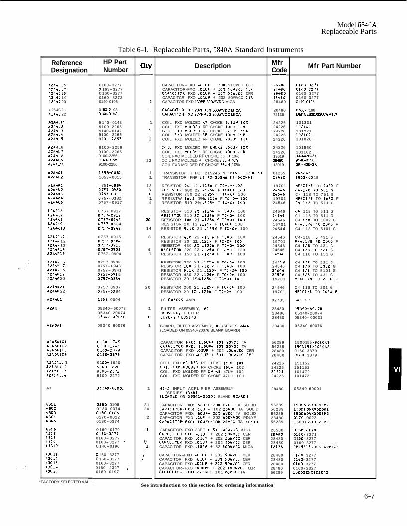
Model 5340A Replaceable Parts
Table 6-1. Replaceable Parts, 5340A Standard Instruments
Reference Designation
AZA4C16 AZC4C17 AZA4Cl8 A2a4C 1 9 A 2A4C 20
A 26 4C 21 A2A4C 22
A2A4L1* A2P4L2 A2A413 AZh414 A2A4L5
A2A 4L6 A2b417 AZA4L8 A2A419 A2A4L10
&2A401 A2A402
AZA4R1 AZA4R2 A2A4R3 A2A4R4 A2A4R5
A2A4R6 A2A4R7 A2A438 A2A4U9 A2A4RlJ
AZA4Rl l A2AM 1 2 A2A4R 13 AZAu114 A2A41115
AZA4R16 A2A4917 A2A4R18 A2A4R19 A 2A 4R 20
A2141121 AZA4R 22
AZA4U1
A21 5
A2A5A1
A2A511C 1 A2A5AlCZ A2A 5AlC3 A2A5AlC4
AZA5AlL 1 A2A 5A 1L 2 A2A5AlL3 AZASA l L 4
A3
A3C1 A3C2 A3C3 A3C4 A X 5
A 3 C 6 A3C7 A3C8 A3C9 A3C10
L 3 C l l A3C12 43C13 A3C14 L3C15
*FACTORY SELECTED VAI
HP Part Number
0160-3277 0 163-3277 0 160-3277 0160- 3272 0140-0195
01 60-21 98 01 40-0193
9 140-0143 9100- 2265 9140-0142 9100- 2265 9 102-2257
9100- 2256 9100- 2265 9100-2256 91404158 9100-2256
1P55-0081 1053-0015
c 75 7 - i 3 8 4 0757- 0920 0 757- 0921 0 75 7- 0 3 82 0757- 0917
0 7 5 7 0917 0757-0917 0757-0948 0757-03 84 0757-0941
0 7 5 7 0915 0757-0384 0751-0915 0757-0908 0 757-0904
0 7 5 7 0908 0757- 0948 0757- 0941 0 757-091 5 0757-0384
0 7 5 7 0907 0 75 7- 03 84
1858 0004
05340- 60078 05340 20074 C 534C-(rOC31
05340 60076
0 100-1745 0180-1745 0160-3879 0160-3879
9 100- 1620 9100-1620 9 1 0 0 - 2 2 u 9100- 2272
05340-60001
0180 0106 0 180- 0374 0180-0106 0170- 0022 0180- 0374
0 160-0179 0160-3271 0160- 3277 0160- 3277 0 140-0196
0 160-3277 0 160-3277 0160- 3277 0160- 2327 ' 0180- 0197 '
QtY -
2
1
1
I
2
23
1 1
1 3 3 1 1 4
20
14
8
4 1
2 0
1
1
1
1
2 1 2 0
2
I
;i i -
Description
CAPACITOR-FXD .01UF +-2OX 51 UVCC CFF CAPACITOR-FXC . D ~ U F + 20% ~ c u v c c C C E CAP4CITDR FXD .OlUF t ZJX S O U V D C CFR CAPACITCR FXO . O I U F + 202 SOWVCC CEC CAPACITOR FXD 130PF 30WVDC MICA
CAPACITOR FXD 20PF -5% 300WVDC MICA CAPACITOR FXD 82PF +5% 300WVDC MICA
COIL FXD MOLDED KC CHOKE 3.311P 10% CCIL FXO MGLDFO RF CHGKE lOUH 102 COIL FXU MOLDtO RF CHCKE 2.2UH 10% COIL FXO MCLDED 9F CHGKE lOUH l'l1 COIL FXD MOLDED RF CHOKE .82UH 1JX
COIL FXD MOLDEO RF CHtlKf -56UH I O X COIL FXO NULDEO RF CHGKE lOUH 1 O X COIL FXO MOLDED RF CHOKE .56UH 10% COIL FXD MOLDED RF CHOKE 3.3UH 10% COIL FXD MOLDED RF CHOKE .56UH 10%
TRANSISTOP J FET 215245 N CHAh 0 M O M 5 1 TRANSISTOR PNP 5 1 PD=ZOOMW FT-SODMHZ
RFSISTOR 26 12 .125W F TC=O+-10? RESISTCP 680 22 .125U F TC=O+-100 RESISTOR 7 5 0 22 .125u F TC=O+ 1 0 0 RFSISTW 16.2 1% -12% F T C = O + . I O D RESISTOR 510 2% .125W F T i - O + 10D
RESISTOR 510 2 2 -12SY F TC=O+ 100 RESISTiYI 510 2 1 -12% F TC-O+ 1 0 0 RESISTOR ~ O K 21 . i25w F TC=O+ 100 RESISTOR 2 0 1 2 .125W F TC=O+ 1 0 0 R E S I S T O R 5.1K 2 1 .125U F TC=O+ 100
RESISTOR '.30 22 .125U F TC=O+ 100 RESISTOR 20 11 .125W F TC=O+ 100 RESISTOR 4 3 0 2 1 . i25w F K=O+ l o o R € S I S T O R 220 22 .125W F T i = O + 130 RESISTOR 150 2 1 .125W F TC-O+ 100
RESISTDR 220 2 1 .125Y F TC=O+ 100 RESISTOR 10K 2 1 .125W F TC=O+ 1 0 0 RESISTOR 5.1K 2 1 -125W F TC=O+-IOO RESISTOR 430 2 2 .125U F TC=O+ 1 0 0 RESISTOR 20 1% .125W F TC=O+ 100
RESISTOR 200 21 .125W F T C = O + 100 RESISTOR 2 0 I2 .125W F 1t-W 100
I C CA3049 AMPL
FILTFR ASSEMBLY, Y2 HOUS INGI FILTFR COVERI HOUSIhG
BOARD, FILTER ASSEMBLY, #2 (SERIES 1344A) (LOADED ON 05340-20076 BLANK BOARD)
CAPACITOR FXD: 1.5UF+ 1 0 1 ZOVOC TA CAPACITOR-FXO: l.SUF+ 102 ZOVOC TA CAPACITOR FXD &1UF + 202 100YVOC CER CAPACITOR FXO . 0 1 U F + 201 l O O W V O C CFR
COIL FXD POLOED RF CHOKE 15UH 10% COIL-FXD MDLOEO RF CHOKE 15UH 102 COIL FXD MOLDED RF CHUKE 47UH 102 COIL FXO MOLDED RF CHOKE 47UH 1 0 1
H I - - 2 INPUT ACPLIFIER ASSEMBLY (SERIES 1348A)
(LOADED ON 0 5 3 4 i - 2 a a o i BLANK BOARD)
CAPACITOR FXO: 60UW-ZOX 6VOC TA SOLID CAPACITDR-FXD: 1OUF+ 102 ZOVDC TA SOLID CAPACITOR FXD: 6OUF+ 201 6VDC TA SOLID CAPACITOR FXD .1UF + 202 6OOYVOC PDLYF CAPACITDR-FXD: lOUF+-102 ZOVDC TA SOL10
CAPACITOR- FXO 33PF + - 5 % 30OUVOC M I C A CAPICITOR-FXD .01UF + 202 50WVDC CER CAPACITOR. FXD - 0 l U F + 202 5OWVDC CER CAPACITOR^ FXO -01UF + 202 50UVOC CER CAPACITOR- FXD 150PF + 52 3OOWVDC MICA
CAPACITOR-FXD -01UF + 202 5OWVDC CER CAPACITOR. FXD -01UF + 20I 5OUVOC CER CAPACITOR-FXD -01UF + 20I 5OYVDC CER CAPACITDR-FXO lOOOPF + 202 lOOYVOC CER CAPACITDR-FXO; 2.2UF+ 1 0 1 20VDC TA
Mfr Code - 2 8 4 ~ 2t14e0 2a4eo 28430 28480
20480 721 36
24226 24226 24226 24226 24226
24226 24226 13019 28480 13019
01255 28480
19701 24546 24546 19701 24546
24546 24546 24546 1 9 7 0 1 24 54 6
24546 19701 24546 24546 2454b
24 5'r 6 24546 24546 245h6 1 9 7 0 1
24 546 19701
02735
28480 28480 28480
28480
56289 56289 28480 28480
24226 24226 2422b 24226
28480
56289 56289 56289 28480 56289
28580 2R4RO 28480 28480 72136
28480 28480 28480 28480 56289 -
Mfr Part Number
0160 3277 0160 3277 0140-0195
01 60-2 198 DM15E82DJ0300WVlCR
101331 101lOZ 101221 101102 101820
101560 101102 09-4426-3K 91400158 08-4426-3K
2N5245 1853-00 15
MF4C118 TO ZORD F T4-118-TO-681-6 C 4 118 TO 7 5 1 G MFCCl18 T O 16R2 F C4 1 1 8 TO 5 1 1 G
C4 118 TO 5 1 1 G C 4 1 1 8 T O 5 1 1 G C 4 118 TO 1002 G MF4C118 T O 20RO F C4 1 1 8 TO 5101 G
C4- 118 TO 4 3 1 G MF4C118 T O 20RO F C4 1 1 8 TO 4 3 1 G C4 1 1 0 TO-221 G C4 1 1 8 TO 1 5 1 G
C4 l l 8 TO 2 2 1 G C 4 1 1 8 T O 1002 G C4 l l 8 TO 5 1 0 1 G C4 1 1 8 TO 4 3 1 G MF4Cl18 T O Z O R O F
C4 1 1 8 TO 201 G MF4C118 TO ZORO F
CA3W9
n534t i -m.78 05340-20074 05340- 00031
05340 60076
15001 55 X902OA2 15OD155X902062 0160 3879 0160 3879
150D6ObXOOO6RZ 0170- 0022 15001 06X902082
D160 0179 0160- 3271 01 60- 3277 0160 3277 OM15F15 1 J0300WVlCR
0160- 3277 0160- 32 77 0160- 3277 0160- 2327 150D225X9020AZ
151152 151152 101472 101472
05340 60001
1500606X0006RZ 15001 06X902002
See introduction to this section for ordering information
6-7
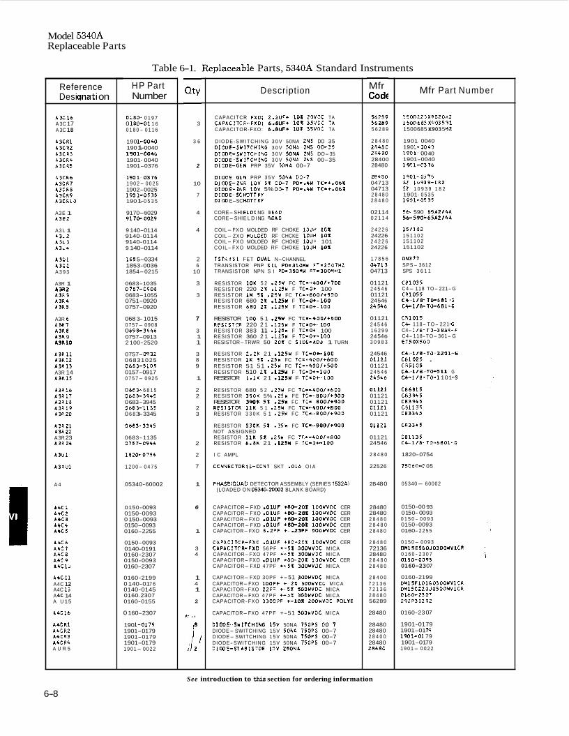
Model 5340A Replaceable Parts
Table 6-1. Fteplaceable Parts, 5340A Standard Instruments
Reference Desi anati on
A 3 C 1 6 A 3C 17 A 3C 18
A3CR1 A3CR2 A3CR3 A3CR4 A3CR5
A3CRb A3CR7 A3CR8 A3CR9 A3CR10
A3E 1 A 3 E Z
A 3 L 1 A 3 L 2 A 3 L 3 A 3 L 4
A 3 9 1 A 3 9 2 A 3 9 3
A3R 1 Am2 A 3 R 3 A 3 R 4 A 3 R J
A3R 6 A 3 R 7 A 3 R 8 A3R 9 A 3 R l O
A 3 R l l A3R12 A 3 R 1 3 A3R 14 A 3 R 1 5
A 3 R 1 6 A 3 R 1 7 A 3 R 1 8 A 3 R 1 9 A3RZO
A 3 R 2 1 A3RZZ A 3R 23 A 3 R 2 4
A 3 U l
A3XU1
A 4
A 4 C l A U Z A 4 C 3 A 4 C 4 A 4 C 5
A K . 6 A 4 C 7 A 4 C 8 A 4 C 9 A 4 C l t i
A k C 1 1 A4C 12 A4C 1 3 A k C 14 A U 15
A U l 6
A 4 C R I A4CRZ A4CR3 AkCR4 A U R 5
HP Part Number
0180- 0 1 9 7 0 180-01 1 6 0 1 8 0- 0 1 1 6
190 1-0040 190 1- 0040 1901-004C1 1901- 0040 1901-0376
1901-,0376 1 9 0 2- 0 0 2 5 1902-0025 190 1-0535 190 1- 0 5 3 5
9170-ti029 9170.0029
9 140-0114 9140-0114 9140-0114 9 140-0114
185 5-0334 1853-0036 1854-0215
0683-1035 0757-0908 0683-1055 0751-0920 0757-0920
068 3- 1015 0 7 5 7- 0 9 0 8 0 69B- 3446 0757-0913 2 100-2520
0757- 0932 06831025 0683-5105 0157-0917 0 7 5 7- 0 9 2 5
0 683- 6 8 1 5 0683-3945 0 683-3945 0683-1135 0 6 8 3- 3345
0683-3345
0683- 1135 0757-094k
1 8 2 0 - 0 7 5 4
1 2 0 0- 0 4 7 5
05340-60002
0 150- 0093 0150-0093 0 150-0093 0150-0093 0160-2255
0150-0093 0140-0191 0160-2307 0150-0093 0160-2307
0160-2199 0 140-01 7 6 0140-0145 0160.2307 0160-0155
0 160-2307
190 1-0179 1901- 0179 1901-0179 1901-0179 1 9 0 1- 0 0 2 2
- QtY -
3
3 6
2
10
7
4
4
2 6
10
3
3
7
3 1 1
3 8 9
1
2 2
2 3
2
2
7
1
6
1
3 4
1 4 1
2
/: ,!
Description
CAPACITCR FXD; 2.2UF+ 101 ZOVDC TA CAPACIVJR-FXD: 6.8UF+ 1 O X 35VOC TA CAPACITOR-FXO: 6.8UF+ lo? 35VOC TA
D I O D E - S W I T C H I N G 3 0 V 50NA ZNS DO 35 OIOOE-SWITCHING 3 0 V 50NA 2NS 00-35 OIOOE-SYITCHING 3 0 V SOYA Z Y S DO-35 O I O O E ~ S W I T C H I N G 3 0 V 50NP 2NS 00-35 DIODE-GEN PRP 35V 50NA 00-7
OIOOE GEW PRP 3 5 V 50NA 00-7 DIODE-ZNR 1OV 5 1 00-7 PD-.4Y T C = + - 0 6 1 DIODE-ZNR 1OV 5% 00-7 PO=.QW TC=+-060 DIODE-SCMITTKY 01 00 E-SC HOTTKY
CORE-SHI E L 0 1 NG BEAD CORE-SHl E L D I NG BEAD
COIL- FXO MOLDED RF CHOKE l O U H 1 C 1 COIL- ZXO MOLGEO RF CHCKE l O U H 101 COIL- FXO MOLOEO RF CHOKE IOUH 101 C O I L- F X O MOLDED R F CHOKE l O U H 101
TSTR:SI FET DUAL N-CHANNEL TRANSISTOR PNP S I L PD-310Mll F T - 2 5 0 7 H l TRANSISTOR NPN S I P0=350NU FT=3OOMHZ
RESISTOR 1 0 K 5 2 .25W FC TC--4001+700 RESISTOR 220 Z X .125W F TC=0+ 100 RESISTOR 1 H 5 1 .25Y FC T C = - 8 0 0 / + 9 0 0 RESISTOR 680 22 - 1 2 5 Y F TCLO+-lOO RESISTOR 6,80 2 1 .125W F TC=O+-100
RESISTOR 100 5 1 .25n FC T C = - ~ O O / + ~ O O RESISTCR 220 2 1 .125Y F TC=O+-100 RESISTOR 383 11 .125Y F TC=O+ 100 RESISTOR 360 2 1 .125Y F TC=O+-100 RESISTOR-TRWR 50 20% C SIDE-AOJ 1 TURN
RESISTOR 2 - Z K 2 1 - 1 2 5 Y F TC=O*100 RESISTOR I K 5 1 .25W FC T C = - 4 0 0 / + 6 0 0 RESISTOR 51 5 1 .25U FC T C = - 4 0 0 / + 5 0 0 RESISTOR 510 2 X . 1 E W F TC=O+-100 RESISTOR 1.1~ 2 1 .i25n F T c = o + - i o o
RESISTOR 680 5 2 .25Y F C T C = - 4 0 0 / + 6 0 0 RESISTOR 3 9 0 K 5% .25Y FE T C = - 8 0 0 1 + 9 0 0 RESISTOR WOK 5 1 .25w FC TC= 8001+9oo RESISTOR 1 1 ~ 5 1 .zsw FC T C = = C O O / + ~ O O RESISTOR 3 3 0 K 5 1 .25W FC T C = - 8 0 0 1 + 9 0 0
RESISTOR 3 3 0 K 5 1 -25W FC T C = , 6 0 0 / + 9 0 0 NOT ASSIGNED RESISTOR 111: 5 I .25W FC T C * - 4 0 0 1 + 8 0 0 RESISTOR 6.8K 21 -125W F T C = O b l O O
I C AMPL
CONNECTOR:l-EONT SKT - 0 1 6 O I A
PHASE/OUAD DETECTOR ASSEMBLY (SERIES 1532A) (LOADED O N 05340-20002 BLANK BOARD)
CAPACITOR- FXD - 0 1 U F +80-20X lOOUVDC CER CAPACITOR- FXO .OlUF +80-20X lOOWVOC CER CAPACITOR-FXO .OlUF +80=20% lOOWVOC CER CAPACITOR- FXD .OlUF +80-201 lOOWVOC CER CAPACITOR-FXO 8.ZPF +-.25PF 5OOYVDC CER
CAPAC1TI)R-FXD - 0 1 U F +80-201 lOOUVOC CER CAPACITDR=FXD 5 6 P F +“51 300YVOC MICA CAPACITOR- FXO 4 7 P F +-5X 3OOYVOC MICA CAPACITOR- FXO .O lUF +80-201 lOOWVOC CER CAPACITOR- FXD 4 7 P F + -51 3OOWVOC MICA
CAPACITOR- FXD 3 0 P F +-51 300WVOC MICA CAPACITOR-FXO l O O P F +-21 300YVOC M I C A CAPACITOR-FXO 2 2 P F C S X 500WVOC MICA CAPACITOR-FXO 4 7 P F +-5X 300WVDC MICA CAPACITOR-FXO 3 3 0 0 P F + - l o t ZOOUVDC POLYE
CAPACITOR-FXO 4 7 P F +-51 300UVOC MICA
OIDOE-SWITCHING 1 5 V 50NA 7 5 0 P S 00-7 DIODE- SWITCHING 1 5 V 5ONA 7 5 0 P S 00-7 DIODE- SWITCHING 1 5 V 50NA 7 5 0 P S 00-7 DIODE- SWITCHING 1 5 V 50NA 750PS 00-7 0IU)E-STABISTOR 1OV 2 5 0 N A
- Mfr Cod€
5 6 2 8 9
5 6 2 8 9
2 8 4 8 0 2R48O 2 R 4 9 0 28400 28480
2R 480 04713 04713 2 8 4 8 0 2 8 4 8 0
02114 0 2 1 1 4
2 4 2 2 6 24226 2 4 2 2 6 24226
1 7 8 5 6 04713 04713
01121 2 4 5 4 6 01121 24 54 6 24546
01121 2 4 5 4 6 1 6 2 9 9 24 54 6 3 0 9 8 3
24546 01121 01121 2 4 5 4 6 24546
01121 01121 01121 0 1 1 2 1 01121
01121
01121 24 54 6
2 8 4 8 0
22526
5 6 2 8 9
28 48 0
28480 28480 2 8 4 8 0 2 8 4 8 0 2 8 4 8 0
2 8 4 8 0 72136 28480 2 8 4 8 0 2 8 4 8 0
2 8 4 0 0 7 2 1 3 6 7 2 1 3 6 2 8 4 8 0 56289
28480
28480 28480 2 8 4 0 0 28480 20480
Mfr Part Number
1 5 0 0 2 2 5 X 9 0 2 0 4 2 1 5 0 D 6 8 5 Xq03 5 8 2 1500685 K903 5 82
1901 0040 190 1- 0040 190 I- 00 40 1901-0040 1 9 C l - C 3 7 6
1 9 0 1 - 0 3 7 5 SL l U 9 3 9 - 1 8 2 57 1 0 9 3 9 1 8 2 1901- 0 5 3 5 1 9 0 1 - 0 5 3 5
56% 590 65A2/W1 5 6 - 5 9 0 - 6 5 A 2 / 4 4
151102 1 5 1 1 0 2 1 5 1 1 0 2 151102
0n377 SPS- 3612 SPS 3 6 1 1
C B 1 0 3 5 C4- 118 TO- 221-G CR1055 C 4 - 1 / 8 - T O - b 8 1 .G C 4 - 1 / 8 - T O - b 8 l - G
C R 1 0 1 5 C4- 1 1 8- T O- 2 2 1 C4- 118-10-3 83R-F C4- 118- TO- 361- G E T 5 0 X 5 0 0
C4-1 /8 -TO-2201-G C 8 1 0 2 5 . C B 5 1 0 5 C 4 - l / & T 0 - 5 1 1 G C4-118- TO-1 101 -G
C 8 6 8 1 5 C 8 3 9 4 5 C 8 3 9 4 5 C 8 1 1 3 5 C 8 3 3 4 5
C 8 3 3 4 5
C 8 1 1 3 5 CC-118-TO-6801-G
1820- 0754
7 5 0 6 0 4 05
05340- 60002
0150-00 93 01 5 0- 00 93 0 1 5 0 - 0 0 9 3 0150-0093 0160- 2 2 5 5
0 1 5 0- 0 0 9 3 OMl5E560J0300WV1CP 0 1 6 0 - 2 3 0 7 0 1 5 0 - 0 0 9 3 0160-23 07
0160-2199 DM15F101G0300WVlCR OM15C220J05OOWVlCR 0 1 6 0 - 2 3 0 1 2 9 2 P 3 3 2 9 2
0160-23 07
1901-0179 1901-01 7 9 1901-01 79 1901-01 79 1 9 0 1- 0 0 2 2
See introduction to this section for ordering information
6-8
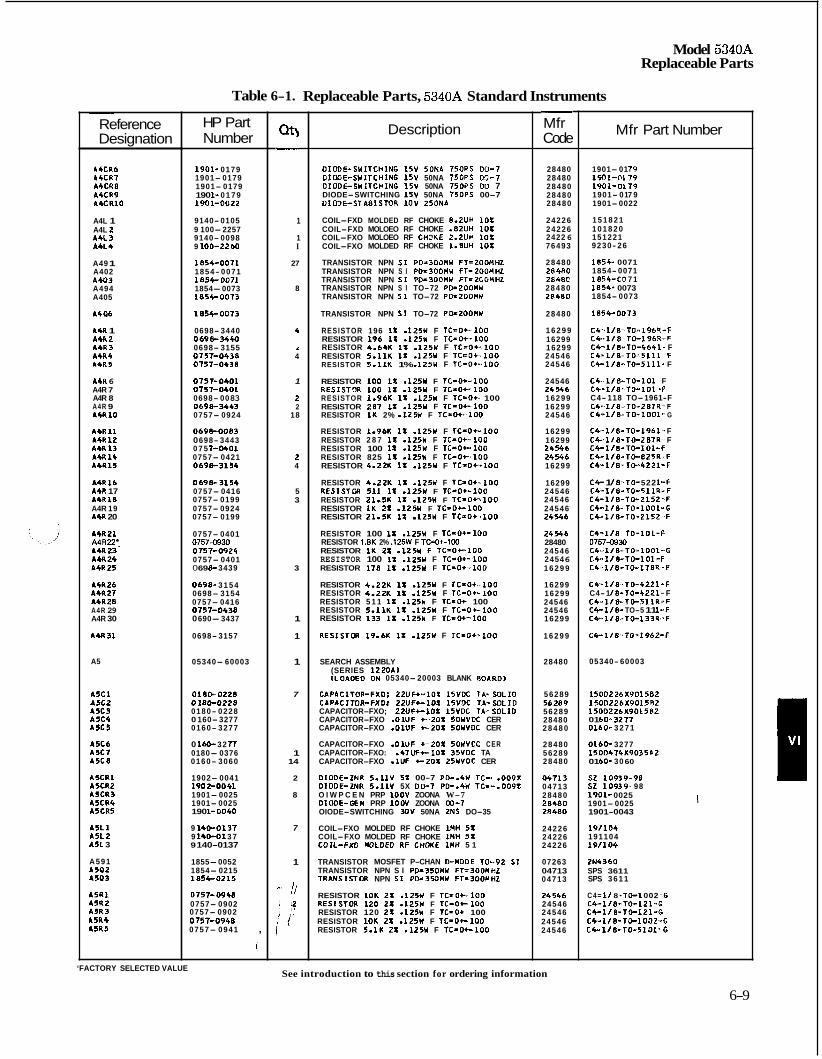
Table 6-1.
Model 5340A Replaceable Parts
Replaceable Parts, 5340A Standard Instruments ~~
Reference Designation
L4CR6 L4CR7 A4CR8 A4CR9 A4CR10
A4L 1 A4L 2 A4L3 A4L4
A49 1 A402 A403 A494 A405
A496
LSR 1 A4R2 A4R3 A4R4 A4R5
A4R 6 A4R 7 A4R 8 A4R 9 AM10
A W 1 1 A4R12 A4R 13 A4R14 AIR15
A4Rl6 A4R 17 A4R18 A4R 19 A M 20
A4R21 A4R22.. A4R23 A4R24 A4R25
A4R26 A4R27 A4R28 A4R 29 A4R 30
A 4 R 3 1
A5
ASCl l 5 C 2 ASC3 A5C4 A5CS
ASC6 A5C7 A5C8
ASCR1 A5CR2 A5CR3 A5CR4 A5CR5
A5L1 A5L2 1%. 3
A591 A592 A593
A5R1 L5R2 A5R3 L5R4 L5R5
HP Part Number
1901- 0179 1901- 0179 1901- 0179 190 1- 0 1 7 9 1901-0022
9140- 0105 9 100-2257 9140- 0098 9 100-2260
1854-0071 1854- 0071 1854- 0071 1854-0073 1854-0073
1854-0073
0698- 3440 0698-3440 0698- 3155 07S7-0438 0757-0438
0757 -0401 0757-0403 0698- 00 83 0696-3443 0757- 0924
0696-0083 0 698- 3443 0 7 5 7-0401 0757- 0421 0698 -3154
0 6 9 8 - 3 1 5 4 0757- 0416 0757- 0199 0757- 0924 0757- 0199
0757- 0401 0757-0930 0757-0925 0757- 0401 0 69 8- 3439
069& 3 1 5 4 0698- 3154 0757- 0416 0757-0438 0 690- 3437
0698- 3157
05340- 60003
0180 -0228 0180-0228 0180- 0228 0 160- 3277 0160- 3277
0 160- 32 77 0180- 0376 0160- 3060
1902- 0041 15’02-0041 1901- 0025 1901- 0025 190 1- 0040
9 140-0137 9 140-01 3 7 9 140-0137
1855-0052 1854- 0215 1854-0215
0757-0948 0757- 0902 0757- 0902 0751-0948 0757- 0941 ,
I
Qt, -
1
1 I
27
8
4
1
4
1
Z 2
18
2 4
5 3
3
1
1
1
7
1 14
2
8
7
1
‘ I /I
/I[
Description
OIOOE-SWITCHING 15V 50NA 750PS 00-7 DIODE-SWITCHING 15V 50NA 750PS 0’)-7 OIOOE-SWITCk+lNG 15V 50NA 750PS 00 7 DIODE-SWITCHING 15V 50NA 750PS 00-7 DIODE-STA8ISTOR 1OV ZSONA
COIL-FXD MOLDED RF CHOKE 8.2UH 10X COIL-FXD MOLOEO RF CHOKE .82UH 1 0 X COIL-FXO MOLOEO RF CH@KE 2-2UH 1 O X COIL-FXO MOLDED RF CHOKE 1.8UH I O X
TRANSISTOR NPN 5 1 P0=3OSMW FT=ZOOMHZ TRANSISTOR NPN S I P0=300MW FT-ZOOMHZ TRANSISTOR NPN S 1 PD-SOOMW FT-ZGOMHZ TRANSISTOR NPN S I TO-72 PO=ZOOMU TRANSISTOR NPN S 1 TO-72 PO=ZOOMW
TRANSISTOR NPN S I TO-72 PDr2OOMN
RESISTOR 196 I t -125Y F TC=O+-lOO
RESISTOR 4.64K 1% .125Y F TC=0+-100 RESISTOR 5.11K 1 8 .125W F TC=O+-lOO RESISTOR 5.11K 1% .125U F TC=O+-lOO
RESISTOR 196 IX . u 5 n F T C = O + - ~ O O
RESISTOR 100 11 . i z 5 n F Tc-o+- ioo RESISTOR l o o 11 . i 2 5 n F TC=O+-IOO
RESISTOR 287 ir .izsw F TC=O+-~OO RESISTOR 1.96K 11 .125W F TCSO+- 100
RESISTOR 1K 2% .125U F TC=O+-100
RESISTOR 1.96K 1X .125W F TC-OClOO RESISTOR 2 8 7 1X .125W F TC-O+-100 RESISTOR 100 1X -125W F TC-0+100 RESISTOR 825 1X .125W F TC-04-100 RESISTOR 4 . 2 ~ ~ 1% .izsw F ~c -o+ - ioo
RESISTLW 511 11 .125w F TC-O+-~OO RESISTOR 4.22K It .125Y F TC-0+-100
RESISTOR 21.SK 1X .l25W F TC-Ot.100 RESISTOR IK zx . i25w F ic=o+-ioo RESISTOR 2 1 . 5 ~ IX .izsw F T C - O + - ~ O O
RESISTOR 100 1% .125W F TC=O+- lOO RESISTOR 1.8K 2% .125W F TC-0t-100
RESISTOR 100 1 X -125W F TC=O+-lOO RESISTOR 1~ t x .izsn F TC=O+-IOO
RESISTOR 178 i x . m y F T C = O + - ~ ~ O O
RESISTOR 4 . 2 2 ~ 11 .im F r c = o + - i o o RESISTOR 4.221: 1X .l25W F 7C=O+-lOO RESISTOR 5 1 1 1% .125W F TC=O+ 100
RESISTOR 133 11 . i 2 5 ~ F TC=O+-~OO RESISTOR 5.11K 1X al25W F T C ~ O C l O O
RESISTMI 19.6K I X .125W F TC-0+-100
SEARCH ASSEMBLY (SERIES 12206 ) ILO&OEO ON 05340- 20003 BLANK 8OAROl
CAPACITOP-FXO: 22UF+-lOX l 5 V K TA- SOLIO CAPACITOR-FXD: 2 2 U F C l O X 15VDC TA-SOLID CAPACITOR-FXO; 22UF+-lOX 15VOC TA- SOLIO CAPACITOR-FXO -0 lUF C Z O X 50YVOC CER CAPACITOR-FXO .OlUF +-201 50WVOC CER
CAPACITOR-FXO .01UF +-2OX 50WVDC CER CAPACITOR-FXO: .47W+-lO% 35VOC TA CAPACITOR-FXO .1UF C Z O X 25YVOC CER
OIOOE-ZNR 5.11V 5 I 00-7 P0=.4IY TC- -009% OIOOE-ZNR 5.11V 5X OW7 PD=.4W TC--.OO9% O I W P C E N PRP lOOV ZOONA W-7 OIOOE-EN PRP 1OW ZOONA W-7 OIODE-SWITCHING 3OV 50NA 2NS DO-35
COIL-FXO MOLDED RF CHOKE 1MH 5 1 COIL-FXO MOLDED RF CHOKE lHH 5 1 c o I L - f x o MOLDED RF cnou i H n 5 1
TRANSISTOR MOSFET P-CHAN 0-MODE TO--92 SI TRANSISTOR NPN S I PD-350MY FT=300HHL TRANSISTMI NPN SI PO=350MW FT=POOMHZ
RESISTOR ~ O K 2 1 .125w F T c - o c i o o RESISTOR 120 zx . i 2 5 n F T C = O + ~ O O RESISTOR 120 Z X -125W F TC=O+ 100 RESISTOR 1OK ZX .125W F TC-OclOO RESISTOR 5. lK ZX .125W F TC-04-100
- Mfr Code
28480 28480 28480 28480 28480
24226 24226 2422 6 76493
28480 28480 2848C 28480 28480
28480
1 6 2 9 9 16299 16299 24546 24546
24546 24546 16299 16299 24546
16299 16299 24546 24546 16299
16299 24546 24546 24546 24546
24546 28480 24546 24 54 6 1 6 2 9 9
16299 16299 24546 24546 16299
1 6 2 9 9
28480
56289 56289 56289 28480 2 8 4 8 0
28480 56289 28480
04713 04713 28480 28480 28480
24226 24226 24226
07263 04713 04713
24546 24546 24546 24546 24546
Mfr Part Number
1901- 01 7 s
1901-0179 1901- 01 7 9 1901- 0022
1 5 1 8 2 1 1 0 1 8 2 0 151221 9230- 26
1854- 0071 1854- 0071
1854- 0073 1854- 0073
1854-0073
C4-118-TO- 1969-F C4-118 TO-196R-F C 4 - l / 8- 10-4641- F CC-118 -TO-5L l l F CC-1/8-TO-5111- F
C4-118-TO-101 F C4-1/8-TO-101 .F C4- 118 TO-1961-F C4-118-TO-287R-F C4-118; TO-1001- G
C+l18-T0-1961- F C C 1/ 8- 10-2 87R- F c4- 118-TO-101-F C4-118-TO-825R-F C4-118-TO.4221-F
C 4 - 1 18- TO- 5 22 l -F C4-118-TO-511R-F C4-118-TO-2152-F C4-118-TO-1001-G CCl18 -TO-2152 -F
C4-118 TO-101-F 0757-0930 C4-118-TO-1001-G C 4 - l l &TO- lO I -F C6118-TO-178Q-F
C4-118-TO-4221-F C4-1 18-10-4221- F
i w i - 0 1 7 9
1854-CP 7 1
C+l18=TD-511R-F C4-118- TO-5 11 l - F C4-1/8-TO-l33R--F
C4- 118- TO-1962-F
05340- 60003
1500226X901582 1500226X901582 150022bK90158Z 01 60- 3277 0160- 3 2 7 1
0160- 3277 1500474X9035 b 2 01 60- 30 60
SZ 1 0 9 3 9 - 9 8 SZ 10939 - 98 1901- 0025 1901- 0025 1901-0043
191104 191104 19 /104
2N4360 SPS 3611 SPS 3 6 1 1
C4= I 1 8 -10-1 002 -G C4-118-TO-121-G C C 11 8- 10-121-6 C4-118-TO-1002-G C4-1/8-10-5101=G
‘FACTORY SELECTED VALUE See introduction to this section for ordering information
6-9
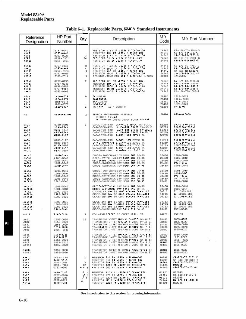
Model 5340A Replaceable Parts
Table 6-1. Replaceable Parts, 5340A Standard Instruments
Reference Designation
A5R6 A 5 R 7 A 5 R 8 A 5 R 9 A5R10
A51711 A5R12 A5R13 A 5 R 1 4 A5R15
A 5 R 1 6 A5R17 A5R18 A 5 R 1 9 A5R20
A 5 U l A5UZ A5U3 A 5 U 4 ASU5
A 6
A 6 C l A 6 C 2 A 6 C 3 A6C4 A6C5
A6C6 A 6 C 7 A 6 C 8 A 6 C 9 A 6 C 1 0
A6CR1 A bCR2 A6CR3 A6CR4 A6CR5
A6CR6 A6CR7 A6CR8 A6CR9 A6CR10
A6CR11 A6CR12 A6CR13 A6CR14 A6CR15
A6CR16 A6CR17 A 6 C R l 8 A6CR19
A 6 L 1
A 6 9 1 A692 A 6 9 3 A 6 9 4 A695
A 6 9 6 A 6 9 7 A 6 9 8 A 6 9 9 A 6 9 1 0
A 6 9 1 1 A 6 9 1 2
A6R 1 A 6 R 2 A 6 R 3 A6R4 A 6 R 5
A6R6 A 6 R 7 A M 8 A 6 R 9 A 6 R 1 0
HP Part Number
0757-0941 0757-0948 0757-0927 0 7 5 7- 0 9 3 1 0 7 5 7- 0 9 3 1
0757-0940 0757-0465 0 7 5 7- 0 9 6 6 0757-0465 2100-2514
0757-0950 0 757-0948 0757-0465 0 75 7-0924 0757-0465
1826-0073 1 8 2 b 0013 1 82 6-0073 1826-0073 1820.0537
05340.60004
0180-0291 018W 1143 018D- 1743 0 1 8 W 1 7 4 3 018C+0197
0180-0197 0180 0197 01 80- 0197 0180-0197 0 1 8 e 0197
190 1-OOkO 190 1-0040 1901-0040 1901-0040 190 1-0010
190 1-0040 1901-0040 1901-0040 1901-0040 1 9 C 1-0040
1901-0040 1901-0040 1902-00 2 5 1902-0025 1902-0025
190 2- 00 2 5 1902-0025 1902-0025 1901-0040
9140-0210
1855-0020 1855-0020 1 855-00 20 1855-0020 1 8 5 5- 0 0 2 0
18 5 5-0020 1855-0020 1855-0020 1 8 5 5 - 0 0 2 0 1855-0020
1855-0020 1855-0020
0 6 9 8 - 3 4 M 0690-3444 0 7 5 7- 0 9 5 5 0 6 9 8- 7 1 8 5 0757-0907
069&7185 0757-0916 0690-71 85 0757-0924 0698-7185 '
- QtY -
3 24
3 4 1
1
2
9
2
1
2
3
12
2
3 1 2
I. I / \
15
ii -
Description
RESISTOD 5.1K 2% -125W F TC=O+l00 RESISTOR 1OK 2 1 .125W F TC=O+-100 RESISTOR 1.3K 2% -125W F TC=O+-100 P.ESISTOR 2 K 2 1 .125W F T C = 0 + - 1 0 0 RESISTOR ZK 2 1 -12% F TC=O+-100
RESISTOR 4.7K 22 .125W F T C = O t - 1 0 0 RESISTOR l O O K 1: .125W F TC=O+-100 RESISTOR 56K 2: .125Y F TC=O+-100 RESISTOR l O O K 11 .125W F T C = O i - l 0 0 RESISTOR-TRMR 2 0 K 101 C S I O E - A O J 1-TURN
R E S I S T M l 1 2 K 2 1 .125Y F T C - W - 100
RESISTOR 1OOK 11 .125W F TC-0-100
RESISTOR 1OOK 11 .125W F TC-0+-100
I C :L INEAR 1C:LINEAR
RESISTOR ~ O K 2: -125W F TC-O+-IOO
RESISTOR i~ 2 1 .USW F ~ c = o + - i o o
I C : L 1 NEAR I C :L I N E A R I C S N 7 4 13 N SCHMITT
SEARCH PROGRAMMER ASSEMBLY ( S E R I E S 1 3 4 4 A ) ILOAOEO ON 05340-20004 BLANK BOARD)
CAPACITOR-FXO; l U F t l O X 35VOC TA- SOLID CAPACITOR-FXO; . l U F + - 1 0 1 35VOC TA- SOLID CAPACITOR-FXO; . l U F + - l O Z 35VOC TA-SOL10 CAPACITOR-FXO; . lUF+-lOZ 35VOC TA-SOL10 CAPACITOR-FXO; 2.2UF+-lOZ 2OVOC TA
CAPACITOR-FXO; 2.2UF+-102 ZOVOC TA CAPACITOR-FXD; 2 . 2 U F t l O l ZOVOC TA CAPACITOR-FXO; 2.2UF+-lOZ ZOVOC TA CAPACITOR-FXO; 2 - Z U F t l O Z ZOVOC TA CAPACITOR-FXO: 2.2UF+-101 20VOC TA
DIODE- SWITCHING 3 0 V 50NA 2NS 00-35 O I W E- S W I T C H I N G 3 0 V 5CNA ZNS 00-35 0100E-SWITCHlNG 3 0 V 50NA 2NS D O- 3 5 CIOOE- SWITCHING 3 0 V 50NA ZNS 00-35 OIOOE- SWITCHING 3 0 V 50NA ZNS 00-35
OIOOE- SWITCHING 3 0 V 50NA ZNS 00-35 DIODE- SWITCHING 3 0 V 50NA ZNS 00-35 DIODE- SWITCHING 3 0 V 50NA 2NS O W 3 5 DIODE- SWITCHING 3 0 V 50NA ZNS 00-35 DIODE- SWITCHING 3 0 V SONA 2NS 30-35
OIOOE-SYITCHING 3 0 V 50NA ZNS 00-35 OIOOE-SYITCHING 3r)V 50NA 2NS 0 0- 3 5 O I O O E Z N R 1OV 5 1 00-7 P 0 s . W TC-+.O61 OIOOE-ZNR 1OV 5 1 O W 7 P0=.4W TC-+.O62 OIOOE-ZNR 1OV 5% 00-7 P0-.4Y TC=+.062
OIOOE-ZNR 1OV 5 1 00-7 P0=.4U TC-+.06% DIODE- ZNR 1 O V 5% 00-7 PD-.kU TC-C-OLZ OIOOE-ZNR 1OV 52 00-7 P0=.4W TC=+.062 OIOOE- SWITCHING 3 0 V 50NA 2NS 00 3 5
COIL- FXD MOLDED RF CHOKE lOOUH 5 1
TRANSISTOR C F E T N-CHIN 0-MODE TO-18 SI TRANSISTOR J- FET N-CHIN 0-MODE 10-18 S I TRANSISTOR J-FET N-CHAN 0-MODE TO-18 S I
TRANSISTOR J-FET N-CHAN 0-MODE TO- 18 5 1
TRANSISTOR J-FET N - C H I N 0-MODE 1 0 - 1 8 51 TRANSISTOR J-FET N-CHAN 0-MODE 10-18 S I TRANSISTOR J-FET N-CHAN 0-MODE TO-18 S I TRANSISTOR J-FET N-CHAN 0-MODE 10-18 S I TRANSISTOR J- FET N-CHAN 0-MODE TO-18 S I
TRANSISTOR CFET N-CHAN 0-MODE 10-18 S I TRANSISTOR J-FET N-CHAN 0-MDOE TO-18 51
TRANSISTOR J-FET N-CHAN 0-nooE TO-18 SI
RESISTOR 316 1% .IZSY F TC-O+-~OO RESISTOR 316 11 .125W F TC=O+-100 RESISTOR 20K 2 1 -125W F TC-O+=100 RESISTOR 220K 5: .125W CC TC=O+1176 R E S I S T C U 200 2: .125W F TC-0+-100
RESISTOR UOK 5 1 .i25n cc ~ c = o + 1 1 7 6 RESISTOR 470 2 1 .125W F TC=O+-100 RESISTOR 2 2 0 K 5% -125W CC T C = 0 + 1 1 7 6 RESISTOR 1 K 2 1 .125W F TC=O+-100 RESISTOR 220K 5 1 .125Y C t TC=O+1176
- Mfr Code - 2 4 5 4 6 2 4 5 4 6 24546 24546 24546
24 54 6 2 4 5 4 6 2 4 5 4 6 24546 30983
24546 24546 2 4 5 4 6 2 4 5 4 6 2 4 5 4 6
28480 28480 2 8 4 8 0 28480 01295
28480
56289 56289 5 6 2 8 9 56289 56289
5 6 2 8 9 56289 5 6 2 8 9 56289 5 6 2 8 9
28480 28480 28480 28480 28480
28480 2 8 4 8 0 28480 28480 28480
28480 28480 04713 04713 0471 3
04713 04713 04713 28480
24226
28480 28480 2 8 4 8 0 28480 28480
28480 28480 28480 28*80 2 8 4 8 0
28480 28480
16299 16299 24546 01121 24546
01121 24546 01121 24 5 4 6 01121
-
Mfr Part Number
C4- 118- TO- 5101- G C4-118-TO-1002-G C 4 - 1 1 8 - T O - 1 3 0 1 - G C 4- 1 1 8- T O- 2 0 0 1- G C 4 - 1 / 8 = T O - 2 0 0 1 - G
C 4 - 1 1 8 TO- 4701- G C4- 1 / 8 - T O - I 0 0 3 - F C4- 1 18- t0-5 6 02-G C 4 = 1 / 8 - T O - I 0 0 3 - F ET50WZ03
C 4 - 1 1 8 - TO- 1202-G C4-118-TO-1002-6 C4-1 /8*TC-1003-F C 4 - 1 / 8 ~ T O - l O O l ~ G C 4- 1 1 8 - T O - 1 0 0 3 - F
1826- 0073 1 8 2 6- 0 0 7 3 1826- 0073 1826-0073 S N 7 4 1 3 N
0 5 3 4 0 - 6 0 n 0 6
1500 105 x903 5 6 2 1 5 0 D 1 0 4 X 9 0 3 5 A Z 1 5 0 0 1 0 4 X 9 0 3 5 A Z 1 5 0 0 1 0 4 X 9 0 3 5 A 2 1 5 0 D 2 2 5 X 9 0 2 O A 2
1 5 0 D 2 2 5 X9020AZ 1 5 0 0 2 2 5 X 9 0 2 0 A 2 1500225 X902 OA2 1 5 0 0 2 2 5 X 9 0 2 0 A 2 1500225 X 9 0 2 OAZ
1901-0040 1901-0040 190 1- 00 40 1901-0@43 1901-0040
1901- 00 10 190 1-0d 40 1901; DO40 1 9 0 1- 0 0 4 0 1901-0040
1901-0040 190 1-00 40 SZ 1 0 9 3 9 . 1 8 2 SZ 10939-182 SZ 10939-182
SL 10939-182 SZ 10939 182 SZ 10939 182 1901-0040
151103
1855- 0020 1855-0020 1855-0020 1855-0020 185 5- 0020
1855-0020 1 8 5 5 - 0 0 2 0 1 8 5 5- 0 0 2 0 1 8 5 5-0020 1855-0020
1855-0020 1855-0020
C4-118-TO-316R-F C4- 118- TO- 316R- F C 4 - 1 1 8 - T O - 2 0 0 2 - G 882245 C4- 118- TO-201-6
882245 C4- 118- T O - 6 7 1 4 882245 C4=1/8*TO-1001-G 882245
See introduction to this section for ordering information
6-10
Model 5340A Replaceable Parts
Table 6-1. Replaceable Parts, 5340A Standard Instruments
Reference Designation
A 6 R l l A6R12 A6R 13
A 6 P 14
A6R15
A 6 R 16 A6R17 A6R18
A6R19 A 6 R 20 A6R21 A6R 22 AbR23
A 6 R 2 4 A 6 1 2 5 A6R26 A6R27 A 6 R 28
A 6R 29 A6R 30 A 6 R 3 1 A 6 R 32 A6R 33
A6R34 A6R 3 5 A6R36 A bR 37 AbR38
A 6 R 3 9 A 6 R 40 A6R41 A 6 R 4 2 A6R43
A6R44 A6R45
A 6 U 1 A6U2 A6U3 A6U4 A6U5
A 7
A7C 1 A7C2 A7C 3 A 7 C 4 A7C5
A7C6 A 7 C 7 A7C8 A7C9 A7C10
A7C 11 A7C12 A7C13 A 7 C 1 4
A7CR1 A 7CR2 A7CR3 A7CR4 A7CR5
A7CRb d 7 C R 7 A7CR8
A7L 1 A 7 L 2 A 7 L 3 A 7 L 4
A 7 0 1 A782 A793 A794 A70 5
HP Part Number
0 7 5 7- 0 9 3 1 0698-7185 0 7 5 7- 0 9 3 5
0 6 9 8 71 85
0 7 5 7 . 0942
0 6 9 8 3 3 7 6 0 6 9 8 - 3 3 76 0698-3376
0698- 3376 0698-3376 0 6 9 8 - 3 3 7 6 0698- 8072 0698-51 82
069&-6242 0 6 9 8 - 5 9 9 6 0 6 9 8 - 5 1 7 5 0698- 5 1 7 4 0 6 9 8 - 7 1 8 5
0698- 71 85 0 6 9 8 - 1 1 8 5 0698-71 85 0 6 9 8- 7 1 8 5 0696-71 85
0 6 9 % = 6 2 9 4 0 698-62 9 4 0698-6294 0 698-62 9 4 0698-6294
0698 6294 0 69 8- 5 9 99 0698-5999 0 6 9 8 - 5 9 9 9 0 6 9 8 - 5 9 9 9
0 6 9 0 - 5 9 9 9 0698-5999
1 8 2 0 - 0 5 7 7 1820- 02 14 1 8 2 5 0 0 5 4 1 8 2 0- 0 7 6 5 1820- 02 07
0 5 3 4 0 - 6 0 0 0 5
0 1 6 0- 0 2 0 5 0 180-0106 0 1 8 0- 0 1 6 0 0 180-01 60 0 160-2230
0 140-01 77 0160-2055 0 1 6 0 - 2 0 5 5 0 1 6 0- 2 0 5 5 0 1 6 0- 2 0 5 5
0180-0117 0180-0374 0160-0138 0 1 8 0 - 1 7 4 3
1 9 0 1- 0 0 4 0 1901-0040 1 9 0 1- 0 0 2 5 1901- 0 0 2 5 190 1- 0025
190 1- 0 0 2 5 1 9 0 1- 0 0 2 5 1 9 0 1- 0 0 2 5
9 140- 0096 9140-0096 9140-0096 * 9 100- 2249
1 8 S f 0 0 2 0 1 8 5 3 - 0 0 2 0 1 8 5 3 - 0 0 3 6 , , 1854- 0215 1 8 5 4 - 0 2 1 5
- QtY -
1
1
6
1
1 1
6
6
1 2
16 1 1
1
1
2
I
1 16
1
1
6
' i / 1
1 1.. -
Description
RESISTOR 2K 21 .125W F TC=O+-100 RESISTOR 22OK 5 1 .125W CC T C = 0 + 1 1 7 6 R E S I S T W 3K 2 1 . 1 2 5 Y F TCqO+-100
RESISTOR 2 2 0 K 5 1 .125W CC T C ~ 0 + 1 1 7 6
RESISTOR 5.6K 2 1 .125W F TC-O+-lOO
FACTORY SELECTED PART
FACTORY SELECTED PART R E S I S T O R 43 5 1 -125W CC TC*0+588 RESISTOR 43 5 1 -125W CC T C = 0 + 5 8 8 RESISTOR 43 5 1 . n 5 w cc TC=O+~WI
RESISTOR 43 5 1 . i 2 5 w cc TC=O+588 RESISTOR 43 5 1 - 1 2 5 Y CC T C * O t 5 8 8 RESISTOR 43 5 1 - 1 2 5 Y CC TC=0+588 RESISTOR 39K 5 1 -125W CC TCmO-850 RESISTOR 3.9K 5 1 .125W CC TC=0+882
RESISTOR 1 .2K 5 1 -125W CC T C 3 0 + 8 8 2 RESISTOR 560 5 1 . i z n cc T C = O + ~ B Z RESI STOR 360 52 .LEV cc TC=O+BBZ RESI STOR zoo 5 1 . i t 5 n cc Tc-o+eet RESISTOR 22OK 5X . 1 2 5 U CC TC-0+1176
RESISTOR 22OK 5 1 .125W CC T C = 0 + 1 1 7 6 RESISTOR 2 2 0 K 51 .125W CC T C = 0 + 1 1 7 6 RESISTOR ZZOK 5 1 - 1 2 5 Y CC T C * 0 + 1 1 7 6 RESISTOR 2 2 0 K 5 1 - 1 2 5 U CC TC=O+1176 RESISTOR 2 2 0 K 5 1 .125U CC T C = 0 + 1 1 7 6
RESISTOR 4 7 K 5f .125W CC TC*0+882 RESISTOR 4 7 K 52 -125W CC TC10+882 RESISTOR 4 7 K 5 1 -125W CC TC*0+882 RESISTOR 4 7 K 5 1 -12% CC TC10+882 RESISTOR 4 7 K 52 - 1 2 5 Y CC TC=O+WZ
R E S I S T W 4 7 K 5 2 . l 2 5 Y CC TC-0+882 RESISTOR 4.7K 52 .125W CC TC=O+BBZ RESISTOR 4.7K 5 1 .125W CC TC-0*882 RESISTOR 4.7K 5 1 .125W CC T C = 0 + 8 8 2 RESISTOR 4 .7K 5 1 .125W CC TC-0+882
RESISTOR 4.7K 5 1 - 1 2 5 Y CC TCPO+882 RESISTOR 4.7K 5 1 .125W CC T C - O t 8 8 2
I C I SN7416N. INVERTER 1C:TTL BCO-T*OECI UAL DECODER IC:SN7400N
1c uv IC sm4 197 N COUNTER
OC AHPLIFIER1COMPENSATOR NO. 1 ASSEMBLY (SEP IES 1 2 2 0 A ) (LOADED ON 05340-20005 BLANK BOARD)
CAPICITOR-FXO l O P F t - 5 % 500WVDC MICA CAPACITOR-FXO; bOUF+-ZOX 6VOC TA-SOL10 CAPACITOR-FXO: 2 2 U F C Z O X 35VDC TA- SOL10 CAPACITOR-FXO: 2 2 U F c Z O Z 35VOC TA-SOL10 CAPAClTOR-FXD 3 3 0 0 P F +-5% 3OOHVDC MICA
CAPACITOR- F X D ~ O O P F + - i x ~ O O Y V O C MICA CAPACITOR-FXD - 0 l U F +80-201 lOOWVDC CER CAPACITOR-FXO . O l U F +80-201 lOOYVOC CER CAPACITOR-FXO .OlUF +80-201 100YVOC CER CAPACITOR- FXD .OlUF +80-201 lOOWVOC CER
CAPACITOR-FXO: 2 . 7 U F C l O Z 35VOC TA CAPACITOR-FXO; lOUF+-101 ZOVOC TA-SOL10 CAPACITOR-FXO - 0 4 7 U F + - l o x ZOOUVDC POLYE CAPAC I TOR-FXD: .lUF+- 101 35VOC TA- SOL I D
OIOOE- SYITCHING 3 0 V 50NA 2NS 0 0 - 3 5 DIODE- SWITCHING 3 0 V 50NA ZNS DO-35 DIODE-GEN PRP lOOV 200NA W-7 OIOOE-GEN PRP lOOV ZOONA 00-7 DIODE-GEN PRP lOOV ZOONA 00-7
DIODE-GEN PRP lOOV ZOONA Do-7 OIOOE-GEN P R P lOOV ZOONA W-7 DIODE-GEN PRP 1 0 0 V ZOONA W-7
COIL- FXD UOLOEO RF CHOKE 1UH 101 COIL- FXO UOLOEO RF CHOKE 1UH 101 COIL- FXO UOLOEO RF CHOKE 1UH 101 COIL- FXO UOLOEO RF CHOKE - 1 5 U H 101
TRANSISTOR PUP 5 1 PD-300UY FT-150HHZ TRANSISTOR PNP S I P0=300MY FT-1SOMHL TRANSISTOR PNP S I L PO=31OMW F T * 2 5 0 7 H L TRANSISTOR NPN SI PO-35OHW FT=300HHZ TRANSISTOR NPN SI, PO-350HU FT-300UHZ
- Mfr Code
2 4 5 4 6 01121 2 4 5 4 6
01121
2 4 5 4 6
01 121 01121 0 1 1 2 1
0 1 1 2 1 O l l Z l 01121 0 1 1 2 1 0 1 1 2 1
0 1 1 2 1 01121 01121 0 1 1 2 1 01121
0 1 1 2 1 01 1 2 1 0 1 1 2 1 01121 01121
01121 0 1 1 2 1 01 1 2 1 0 1 1 2 1 0 1 1 2 1
0 1 1 2 1 01121 01121 01121 01121
01 1 2 1 0 1 1 2 1
0 1 2 9 5 0 1 2 9 5 0 1 2 9 5 0 1 2 9 5 07263
2 6 4 8 0
2 8 4 8 0 56289 56289 56289 28480
7 2 1 3 6 28480 2 8 4 8 0 28480 28480
56289 56289 28480 5 6 2 8 9
28480 2 8 4 8 0 28480 28480 28480
2 8 4 8 0 2 8 4 8 0 28480
2 4 2 2 6 2 4 2 2 6 2 4 2 2 6 24226
28480 28480 04713 04713 0471 3 -
~~ ~ ~~
Mfr Part Number
C4- 118-10-2001-6 0 8 2 2 4 5 CC-118. TO- 3001- 6
0 0 2 2 4 5
C 4 - ~ 1 1 8 - T O - 5 6 0 1 ~ G
B R 4 3 0 5 8 8 4 3 0 5 8 8 4 3 0 5
8 8 4 3 0 5 8 8 4 3 0 5 8 8 4 3 0 5 883935 6 8 3 9 2 5
8t) l tZS 8 8 5 6 1 5 883615 8 8 2 0 1 5 8 8 2 2 4 5
8 8 2 2 4 5 8 8 2 2 4 5 8 8 2 2 4 5 8 8 2 2 4 5 8 6 2 2 4 5
8 6 4 7 3 5 6 8 4 7 3 5 884735 8 8 4 7 3 5 8 8 4 7 3 5
8 8 4 7 3 5 8 6 4 7 2 5 6 6 4 7 2 5 6 8 4 7 2 5 8 8 4 7 2 5
8 8 4 7 2 5 8 6 4 7 2 5
SN7416N SN7442N S N 7 4 0 0 N S N 7 4 1 9 7 N 9 6 0 1 P C
0 5 3 4 0- 6 0 0 0 5
0 1 6 0- 0 2 0 5 15006@5X000682 1 5 0 0 2 2 6 X 0 0 3 5 R 2 1 SOD22 6 X0035R 2 0160-2230
OH1 5F401F0300WVlCR 0160-2055 0 1 6 0- 2 0 5 5 0 1 6 0- 2 0 5 5 0 1 6 0- 2 0 5 5
1 5 0 0 2 7 5 X 9 0 3 5 8 2 15001 06X902082 0160- 01 38 1 5 0 0 1 W X 9 0 3 5 A Z
1901-0040 1901-0040 I 1 9 0 1- 0 0 2 5 1 9 0 1- 0 0 2 5 1 9 0 1- 0 0 2 5
I
1 9 0 1 - 0 0 2 3 1x1-0025 1 9 0 1- 0 0 2 5
1 5 1 1 0 1 1 5 1 1 0 1 151101 1 0 1 1 5 0
18 53- 002 0
SPS- 3612 SPS 3611 SPS 3611
1853-0020
I
See introduction to this section for ordering information
6-1
Model 5340A Replaceable Parts
Reference Designation
A 7 0 6 A 7 P 7 A 7 0 8 A 7 P 9
A 7 1 1 A 7 R 2 A 7 R 3 A 7 R 4 A 7 R 5
A 7 R 6 A 7 R 7 A 7 R 8 A 7 R 9 A7R10
A 7 R l l A 7 R 1 2 A 7 R 1 3 A7R 14 A I R 15
A7R 16 A7R 17 A 7 R 1 8 A 7 R 1 9 A 7 R 2 0
A 7 R 2 1 A7R 22 A7R23 A7R 24 A 7 R 2 5
A 7 R 2 6 A7R27 A7R28 A I R 29 A 7 R 3 0
A7R 31 A I R 32 A 7 1 3 3 A 7 R W A 7 1 3 5
A 7 T P 1 A7TP2 A7TP3 A 7 T P 4 A 7 T P 5
A7TP6 A 7 T P 7
A 7 U 1
A 8 C 1 A n t 2 A 8 C 3 A l C 4 A 8 C 5
A 8 C 6 A l C 7 ABCB A 8 C 9 A 8C 10
A 8 C l 1 A l C 1 2 A 8C 13 A l C 1 4 A 8 C 1 5
A 8 C 1 6 A l C 17 A8C18 A 8 C l 9 A 8C 20
A I C Z 1 A 8 C 2 2 A 8 C 2 3
Table 6-1.
HP Part Number
1 8 5 4 0 2 1 5 1854-0215 1854-0215 1853-0036
0 6 9 8 = 3 4 5 1 0757-0924 0757-0416 0757-0931 0751-0948
0698- 3260 0757-0932 0684.2005 0757-0316 0757-0421
0757- 0952 0757-09 5 2 2 100-2574 0 7 5 7- 0 9 3 1 0757-0931
0 7 5 7- 0 9 3 1 0757-0931 0 7 5 7-0949 0757-0941 0 7 5 7- 0 9 3 1
0683-0685 0757-0924 0757-0952 0757-0316 2100-2517
0757-0931 2300-2632 0 75 7- 09 41 0 7 5 7- 0 9 2 3 0757-0948
0757-0924 0757-0378 0683-0685 0757-0931 0757-0941
0360-0124 0360-0124 0 360-0124 0 36W 0124 0360-0124
0 3 6 0 0 0 1 2 4 0 3 60- 0124
182bW21
0 5 3 4 0- 6 0 0 0 6
0160-2227 0180-0374 0180-0374 0180-0374 0180-0374
0160-3060 0160-3060 0160-3060 0160-3060 0160-0161
0140-0221 0160-01 61 0160-3060 0160-0161 0160-2220
0 160-3060 0 160-3060 0 140-0234 0160-0174 4
0160-3060
0160-3060 0 180-022e 0180-0210
Replaceable Parts, 5340A Standard Instruments
QW -
1
1
1 2
4
5
1
3
2
2
1
1
19
2
I
1
3
1
1
1 P r r 1 t
1 ; ii 3
-
Description
TRANSISTOR NPN SI PO-35OMW FT=3YOMhZ TRANSISTOR NPN S I POn350HW FT-JOOMHZ TRANSISTOR NPN S I P0-350HW FT=3OOMHL TRANSISTOR PNP S I L P01310MW FT-2507HZ
RFSISTOR 1 3 3 K 12 .125W F TC=O+-lOO RESISTOR 1 K 22 .125W F TC=O+-100 RESISTOR 511 12 -125W F T C l O + - 1 0 0 RESISTOR 2 K 2 X -125W F TC-O+- lOO RESISTOR IOK 22 .125Y F TC=O+ 100
RESISTOR 464K 12 - 1 2 5 Y F TC=O*-100 RESISTOR 2.2K 2 1 -125W F TC=O+-100 RESISTOR 20 52 .25W FC T C - - 4 0 0 / + 5 0 0 RESISTOR 42.2 1 X .125W F TC=O+-lOO RESISTOR 825 ix .125W F T C = O + - ~ O O
RESISTOR 1 5 K 22 -125W F TC-0+-100 RESISTOR 1 5 K 22 .125W F TC=O+ 100 RESISTOR-TRMR 500 1OX C SIDE- AGJ 1-TURN RESISTOR 2K 22 .125W F TC=O+-lOO RESISTOR 2 K 22 .12% F T C = 0 + - 1 0 0
RESISTCR 2 K 21 . l 2 5 Y F TC-0+-100 RESISTOR Z K 2X .125U F TC=0+-100 RESISTOR 1 1 K 2X .125U F TC.-O+.100 RESISTOR 5.1K 22 .125W F TC=O+-100 RESISTOR ZK 22 .125W F TC-O+-100
RESISTOR 6.8 5 X -25W FC T C * - 4 0 0 / + 5 0 0 RESISTOR 1K 22 .125W F TC=O+lOO RESISTOR 1 5 K 22 -125W F TC*O+ 100
RESISTOR-TRMR 50K 101 C SIDE-ADJ I - T U R N RESISTOR 42.2 12 .125W F TC-O+-~OO
RESISTOR 2 K 2X .125W F T t = 0 + - 1 0 0 RESISTOR-TRHR 100 10% C S I D E- A O J 1-TURN RESISTOR 5.M 22 .125W F TC-Of-100 RESISTOR 910 2 X - 1 2 5 Y F TC=O+-lOO RESISTOR 1OK 22 -125Y F TC=0+-100
RESISTOR 1K 22 -12% F TC=O+-100 RESISTOR 11 1 X .125W F TC=0+100 RESISTOR 6.8 5 X -2% FC TC=-4001+500 R E S I S T W 2K 22 -125Y F TC=0+-100 RESISTOR 5.1K 22 -125W F TC-O+-100
TERMINAL- STUD SPCL PRESS HTG TERMINAL-STUO SPCL PRESS MTG TERMINAL-STUO SPCL PRESS MTG TERMINAL- STUD SPCL PRESS MTG TERMINAL- STUD SPCL PRESS MTG
TERMINAL-STUO SPCL PRESS MTG TERHINAL-STUD SPCL PRESS HTG
IC VOLTAGE FOLLOWER
BANOPASS F I L T E R 1 P H A S E DETECTOR ASSEMBLY ( S E R I E S 1 2 2 0 A ) (LOADED ON 05340-20006 BLANK BOAR01
CAPACITOR-FXO 2 4 0 0 P F +-52 300WVOC M I C A CAPACITOR-FXO; l O U F + - l O X ZOVOC T I * SOL10 CAPACITOR-FXO: l O U F + - l O X 2 0 V X T A- S O L I D CAPACITOR-FXO: l O U F * - I O X ZOVOC TA- K l L l O CAPACITOR-FXO: lOUF+-IO2 ZOVOC T A - S O L 1 0
CAPACITOR-FXO . lUF +-201 25WVOC CER CAPACITOR-FXO -1UF +-202 25WVOC CER CAPACITOR-FXO .1UF +-201 25YVOC CER CAPACITOR- FXO -1UF +2O% 25WVOC CER CAPACITOR- FXD .01UF +*IOI ZOOWVDC POLYE
CAPACITOR- FXO 2 2 O P F +12 JOOWVOC MICA CAPACITOR- FXD .O lUF +-lo1 200WVDC POLYE CAPACITOR-FXO - 1 U F C Z O X 25WVOC CER CAPACITOR- FXD .01UF c 1 O X 2OOWVOC POLYE CAPACITOR-FXO l 2 W P F +-52 300YVOC MICA
CAPACITOR- FXO -1UF +-202 25YVOC CER CAPACITOR-FXO -1UF 6 2 0 2 25WVOC CER CAPACITOR-FXO SOOPF +-12 300WVOC M I C A CAPACITOR-FXO - 4 7 U F +SO-202 25YVOC CER CAPACITOR-FXO -1UF +-202 25WVOC CER
CAPACITOR- FXO -1UF +-201 25WVOC CER CAPACITOR-FXOI 2 2 U F + - 1 0 2 15VDC TA-SOL10 CAPACITOR-FXO: 3.3UFi-201 l 5 V D C TA
- Mfr Cod€ - 04713 0 4 7 1 3 0 4 7 1 3 04713
16299 24546 24546 24 546 24546
03888 24546 01121 24546 24%6
24546 24546 3 0 9 8 3 24 54 6 24546
24546 24546 24546 24546 24546
01121 24546 24546 24546 3 0 9 8 3
2 4 5 4 6 30983 24546 24546 24546
24546 19701 01121 24546 24546
28480 28480 28480 2 8 4 8 0 2848C
28480 28480
27014
2 8 4 ~ 0
28480 5 6 2 8 9 5 6 2 8 9 56289 56283
28480 28480 28480 28480 56289
72136 56289 28480 56289 2 8 4 8 0
28480
72136 56289 2 8 4 8 0
2 8 4 8 0 5 6 2 8 9 5 6 2 8 9
Z R ~ B O
-
Mfr Part Number
SPS 3 6 1 1 SPS 3611 SPS 3 6 1 1 SPS- 361 2
C4- 11 8- TO-1 333- F C 4- 1 1 8- T O- 1 0 0 1 G C 4 - 1 1 8 TO- 511R F C 4 - 1 / 8 TO- 2001- G C4-118-TO-1002-G
PME55S c4= i / n L i 0 - z 2 o i . G C 8 2 0 0 5 C4-118-TO-42RZ-F C 4 - 1 1 8 - T O - 8 2 5 R - F
C C 1 1 8 - 7 O r 1 5 0 2 G C 4 - 1 / 8 - 1 0 - 1 5 0 2 - G E T 5 0 X 5 0 1 C4- 1 18 . TO- 2001- G C 4 - 1 1 8 - T O- 2 0 0 1- G
C4-118-TO-2001-G C C 1 1 8 - T O - 2 0 0 1 - G C4- 118- TO- 1102- G C C 118- TO- 51 01-G C+.118-TO-ZOOl-G
C 8 6 8 G 5 C 4 - 118- TO- 1 001-6 C4- 118 .TO-1502-G C 4 - - 1 / 8 - TO-42P.Z- F E T 5 0 X 5 0 3
C4-118-TO-2001-G E T 5 0 X 1 0 1 C Q 1 1 8 - T O - 5 1 0 1 - G C4-118-TO-911-G C4-118-TO-1002-G
C + 1 / 8 - T O - 1 0 0 1 - G MF4C1/8-TO llRO F C 8 6 8 G 5 C 4 - 1 1 8 - T O - 2 0 0 1 - G C4-118-TO-5101-G
0360-* 01 24 0360-0121 036.0-01 24 0360-01 24 0 3 6 0- 0 1 2 4
0360-0124 0360-01 24
L M 3 1 0 H
0 5 3 4 0 - 6 0 0 0 6
0 1 6 0 - 2 2 2 7 15001 o b X 9 0 2 0 8 2 1 5 0 D 1 O b X 9 0 2 0 8 2 1 5 0 D 1 0 6 X 9 0 2 0 8 2 1 5 0 0 1 0 6 X 9 0 2 0 8 2
0160-3060 0160- 3060 0160-3060 01 6 0- 30 60 292 P 1 0 3 92
OM1 5 F 2 2 1 F 0 3 OOWVlC 2 9 2 P 1 0 3 9 2 0160-30 60 2 9 2 P 1 0 3 9 2 0 1 6 0- 2 2 2 0
0 1 6 0 - 3 0 6 0
016 0-30 60 1 5 0 0 2 2 6 X 9 0 1 5 8 Z 1 5 0 0 3 3 5 X 0 0 1 5 A 2
I
See introduction to this section for ordering information
6-12
Model 5340A Replaceable Parts
Table 6-1. Replaceable Parts, 5340A Standard Instruments ~
Reference Designation
A8CR1 A8CR2 A8CR3
A8L 1 A 8 L 2 A 8 L 3 A 8 L 4
ASP1 A 8 0 2
A8171 A8R2 A8R3 A8R4 PER5
A 8 R 6 A8R7 A8R8 A8R9 A8R10
A817 11 A8R12 A 8R 13 ABR14 A8R15
A8R16 ABR17 A 8 R l 8 A8R19 A8RZO
A 8 R 2 1 A8R22 A8R23 A8R24
A 8 U 1 A8UZ A 8 U 3
A 9
A9C 1 A9C2 A9C3 A 9 C 4 A9C5
L 9 C 6 A9C7 A9C8 A9C9 A 9 C 1 0
A 9 C l l A9C 12 A9C13
A 9 C R l A9CR2
A 9 L 1 A 9 L 2 A 9 L 3 A 9 L 4
A 9 Q 1 A9P2 A903
A 9 R 1 A9R2 L 9 R 3 A 9 R 4 A9R5
A9R6 A9R7 A9R8 A9R9 A9R10
HP Part Number
1 9 0 2 - 3 1 82 190 2-00 2 5 1 9 0 2- 0 0 2 5
9 140-0118 9 140-0118 9 1 4 0- 0 1 1 8 9 1 4 0- 0 1 1 8
1855-0334 1 8 5 5- 0 3 8 0
0 6 9 8 - 3 1 5 0 0 7 5 7- 0 9 3 4 0698-3433 0 6 9 8 - 3 1 5 5 0 7 5 7- 0 4 2 4
0 7 5 7 - 0 9 1 1 0 7 5 7 - 0 3 8 5 0 6 9 8 - 3 1 32 0 7 5 7- 0 4 2 4 0 7 5 7 - 0 9 5 8
0698-3433 0 7 5 7- 0 9 2 4 2 1 0 0- 2 5 7 4 0683-1OS5 0 7 5 7- 0 9 31
0 7 5 7- 0938 0 7 5 7- 0 9 4 0 0 7 5 7- 0 9 4 0 0683-1055 0 7 5 7 - 0 9 4 8
0 7 5 7- 0 9 2 2 0 7 5 7- 0 9 2 2 0 6 9 0 - 3 4 4 6 0698-3446
1826- 0073 1 8 2 0 - 0 4 7 5 1 8 2 0 - 0 5 1 5
0 5 3 4 0- 6 0 0 0 7
0 1 8 0 - 0 1 9 7 0180-0197 0 1 8 0- 0 1 9 7 0160-0153 0 1 8 0- 0 2 2 8
0180-0230 0 1 8 0- 0 2 2 8 0 1 7 0- 0 0 2 2 0 160-03 62 0180-0230
0160-0362 0180-0197 0 1 8 0 - 0 1 9 7
190 1-0040 1 9 0 1- 0 0 4 0
9140-0096 9 1 4 0- 0 0 9 6 9 1 4 0- 0 0 9 6 9 1 0 0- 2 2 8 8
1854-0215 1 8 5 4- 0 2 1 5 1 8 5 3- 0 0 3 6
2 100-1661 0 7 5 7- 0 9 3 1 0683-2745 2 1 0 0- 2 5 1 7 0 7 5 7- 0 9 2 4
3 7 5 7 - 0 9 4 8 3 7 5 7 - 0 9 4 8 ' 3 7 5 7- 0 9 6 5 3 7 5 7- 0 9 3 1 1 7 5 7- 0 9 2 4
1
QtY
2
4
1
3 7 2
2
3 1 1
1
5
2 3
1
1
3
2
1
1
1
' i, I j3
Description
DIODE- ZNP 1 Z . l V 5X 00-7 PD=.4W TC=+.O64X OIOOE-ZNR 1OV 5X 00-7 PD=.4W TC=+.06X DIODE-ZNR 1OV 5 1 00-7 P0-.4U TC=+.ObI
COIL- FXO MOLDED RF CHOKE 5 0 0 U H 5 X COIL- FXD HDLCED RF CHOKE 5 0 0 U H 5 1 COIL-.FXD WJLDEO RF CHOKE 5 0 0 U H 5X COIL- FXD MOLDED RF CHOKE 500UH 5 1
TSTR:SI FET W A L N-CHANNEL TRANSISTOR HCSFET 2 N 4 3 5 1 N-CHAN E-MODE
RESISTOR 2.37K I2 .125W F T C - O t 1 0 0 RESISTOR 2.7K 2 2 .125W F TC=0+-100 RESISTOR 28.7 1 X . 1 2 5 U F TC-04-100 RESISTOR 4.641: I t - 1 2 5 Y F TC-O+-lOO RESISTOR 1.1K 1X .125W F TC-0t-100
RESISTOR 300 2 X -125W F TC-D+-100 RESISTOR 22.1 1 2 .125Y F TC=Ot-lOO RESISTOR 2 6 1 I1 - 1 2 5 U F TC-0+-100 RESISTOR 1.1K 1% .125Y F T C = O c l O O RESISTOR 1DK 2 1 .125W F TC=O+-100
RESISTOR 28.7 it . i 2 5 w F ~ c - o c i o o
RESISTOR 111 52 .25n FC T C = - ~ O O / + ~ O O
RESI-STOR 1 K 2 1 - 1 2 5 U F TC=O+-100 RESISTOR-TRWR 500 101 C SIDE- ADJ 1-TURN
RESISTOR 2 K 2 X .125W F TC=O+-100
RESISTOR 3 .9K 2% .125Y F TC=Oi-lOO RESISTOR 4.7K 21 .125W F TC-04-100 RESISTOR 4.7K 2 1 .125U F TC-O+-100 RESISTOR 1 H 52 .25W FC T C = - 8 0 0 / + 9 0 0 RESISTOR ~ O K 2 1 . i 2 5 w F TC=O+-IOO
RESISTOR 820 2 x . i 2 5 w F TC-O+-IOO RESISTOR 383 12 .iz5w F TC=O+-IOO RESISTOR 3 8 3 11 -125W F T C = 0 + - 1 0 0
RESISTOR 820 22 .125W F T C - O c 1 0 0
1C:LINEAR 1C L M 3 0 6 H COHPTR I C HV
DC AWPLIFIER/CWPENSATOR NO. 2 ASSEMBLY ( S E P I E S 1 2 2 0 A I (LOADED CN 0 5 3 4 0- 2 0 0 0 7 BLANK 8DARDl
CAPACITOR-FXD; 2.2UF+-102 ZOVDC TA CAPACITOR-FXD: 2 . 2 U F + - 1 0 2 ZOVDC TA CAPAClTDR=FXD; 2.2UF+=102 ZOVOC TA CAPACITOR-FXD 1OOOPF'+-1OI ZOOWVOC PDLYE CAPACITOR-FXD; ZZUF+-lOX 15VDC TA-- SOL I D
CAPACITOR-FXO: l U F t Z O 1 50VDC TA-SOL I D CAPACITOR-FXO; 22UFi-1OX 15VDC TA SOL10 CAPACITOR-FXD - 1 U F C Z O X 600YVOC PDLYE CAPACITOR-FXD 5 1 0 P F +-5X 3OOWVDC MICA CAPACITOR-FXDi 1UFt-202 50VDC T A - S O L I D
CAPACITOR-FXD 5 1 0 P F + 5 2 3OOWVOC MICA CAPACITOR-FKD; Z.ZW*; 101 2OVDC T I CAPACITOR-FXD: Z.ZUF+-lOZ ZOVDC TA
OIDDE- SWITCHING 3 0 V 50NA 2NS 00-35 DIODE- SWITCHING 3 0 V 50NA 2NS 00-35
COIL- FXO MOLOEO RF CHOKE I U H 101 COIL- FXD MOLDED RF CHOKE 1UH 1 0 X COIL- FXD MOLDED RF CHOKE 1UH 101 COIL- FXD MOLDED RF CHOKE I H H 1OX
TRANSISTOR NPN SI PO-350MW FT-300HHL TRANSISTOR NPN S I PO=350MU FT=3OOMHZ TRANSISTOR PNP S I L PO-31OHW FT-2507HZ
RESISTOR-TRHR ZOK R YY SIDE-ADJ RESISTOR 2 K 2 1 .12W F T C - 0 c - 1 0 0 RESISTOR 2 7 0 K 5 X .25W FC TC=-800/+900 RESISTOR-TRMR 501: 10% C SIDE- ADJ 1-TURN RESISTOR 1 K 22 -125W F TC=0+-100
RESISTOR 1 0 K 2 X - 1 2 5 Y F 1C-W 100
RESISTOR 5 1 K 22 .125W F T C - O c 1 0 0 RESISTOR ZK 2 2 .125W F TC=0+-100 RESISTOR 1 K 22 .12W F TC-O+-100
RESISTOR IOK 21 . i z 5 n F T c - o c i o o
- Mf r Code
0 4 7 1 3 0 4 7 1 3 04713
2 4 2 2 6 2 4 2 2 6 2 4 2 2 6 2 4 2 2 6
1 7 8 5 6 0 4 7 1 3
1 6 2 9 9 24 5 4 6 03888 1 6 2 9 9 2 4 5 4 6
2 4 5 4 6 19701 1 6 2 9 9 2 4 5 4 6 2 4 5 4 6
03 88 8 2 4 5 4 6 3 0 9 8 3 01121 2 4 5 4 6
2 4 5 4 6 2 4 5 4 6 2 4 5 4 6 01 12 1 2 4 5 4 6
2 4 5 4 6 2 4 5 4 6 1 6 2 9 9 16299
2 8 4 8 0 2 7 0 1 4 0 7 2 6 3
2 8 4 8 0
5 6 2 8 9 5 6 2 8 9 5 6 2 8 9 5 6 2 8 9 5 6 2 8 9
5 6 2 8 9 5 6 2 8 9 2 8 4 8 0 2 8 4 8 0 56289
2 8 4 8 0 5 6 2 8 9 5 6 2 8 9
28480 2 8 4 8 0
24226 2 4 2 2 6 2 4 2 2 6 0 6 5 6 0
04713 04713 04713
3 2 9 9 7 2 4 5 4 6 01121 30983 2 4 5 4 6
2 4 5 4 6 2 4 5 4 6 2 4 5 4 6 2 4 5 4 6 2 4 5 4 6
-
Mfr Part Number
SZ 1 0 9 3 9 , 2 0 6 SZ 1 0 9 3 9 - 1 8 2 SZ 1 0 9 3 9 . 1 8 2
1 9 / 5 0 3 1 9 / 5 0 3 191 5 0 3 1 9 / 5 0 3
0n377 2 N 4 3 5 1
C4-118-TO-2371-F C 4 - 1 / 8 - 1 0 - 2 7 0 1 - G PHE55-118-TO 28A7 ,F C 4- 1 1 8- T O- 4 6 4 1 - F C 4 - 1 / 8 - T O - 1 1 0 1 - F
C4-118-TO-301-G M F 4 C l / 8 - T O = 2 2 R l - F C C 1 / 8 - T O - 2 6 1 0 - F C4-1 /8 -TO-1101-F C4-1 /8 -TO-1002-G
P M E 5 E l / B - T 0 28R7-F C C 1 / 8 - T O - l 0 0 1 - G E T 5 0 X 5 0 1 C 8 1 0 5 5 C4-1 /8 -TO-ZOOl-G
C 4 - 1 / 8 - T 0 - 3 9 0 1 - G C4-1 /8 -TO-4701-G C 4 - I / & T 0 - k 7 O l - G C B 1 0 5 5 C4-1 /8 -TD-1002-G
C4-1/8-TO-821-G C 4- 1 1 8- T O- 8 2 1 -G C4-118-10-383R- F C C 1 / 8 TO-383R-F
1 8 2 6- 0 0 7 3 LM306H 9 6 0 2 P C
05340-60007
1 5 0 0 2 2 5 X902 OAZ 1 5 0 0 2 2 5 X 9 0 2 0 A 2 1 5 0 0 2 2 5 X 9 0 2 0 A Z 2 9 2 P I 0 2 9 2 1 5 0 0 2 2 6 X 9 0 1 5 8 2
1 5 0 0 1 0 5 X 0 0 5 0 A Z 1 5 0 D 2 2 6 X 9 0 1 5 8 2 0 1 7 0- 0 0 2 2 0160- 0362 15001 0 5 X 0 0 5 0 A Z
01 60- 0362 1 5 0 0 2 2 5 X 9 0 2 0 A 2 1 5 0 D 2 2 5 X 9 0 2 0 A Z
1901-0040 1901-0040
I 15/101 1 5 / 1 0 1 151101 09-AlO2K
SPS 3 6 1 1 SPS 3611 SPS- 3612
3057P-1-203 C4-1 /8 -TO-ZOOl- t C 8 2 7 4 5 ETSOX503 C4-1 /8 -TD-1001-G
C C 1 / 8 - T O - 1 0 0 2 - G C4-118- TO- 1002- C C1- 1 /8- t0-5 102-C C 4 - 1 / 8 - T O - 2 0 0 1 - G C4==1/8- T O- 1 0 0 1- 6
I
See introduction to this section for ordering information
6-13
Model 5340A Replaceable Parts
a
Reference Designation
A 9 R 1 1 A 9 R 1 2 A 9 R 1 3 A9R 14 A 9 R 1 5
A 9 R 1 6 A 9 R 1 7 A 9 R 1 8 A 9 R 1 9 A 9 R 2 0
A 9 T P 1 A 9 T P 2 A 9 T P 3 A 9 T P 4
A 9 U 1 A 9 U 2 A 9 U 3 A 9 U 4 A 9 U 5
A 9 U 6
A 1 0
A l O C l A l O C 2 A l O C 3 A l O C 4 A l O C S
A l O C 6 A l O C 7 A I O C 8 A l O C 9 A I O C 1 0
A 1 0 C l l A l O C 1 2 A 1 0 C 1 3 A l O C l 4 A l O C l S
A I O C l 6
A I O C R 1 A l O C R 2 A l O C R 3 A l O C R W A lOCRSa
A l O L 1 A l O L 2 A l O L 3 A l O L 4 A l O L 5
A l O L 6 A l O L 7 A l O L 8 A l O L 9 A l O L 1 0
A l O M P l
A 1 0 0 1 A 1 0 0 2 A 1 0 0 3 A 1 0 0 4 A 10 05
A 1 0 0 6
A l O R 1 A l O R 2 A 1 0 R 3 A 1 0 R 4 A 1 0 R 5
A l O R 6 A 1 0 R 7 A l O R 8 A 10R9 A l O R l O
-
IOCR4, AlOCRS. A l Z C R l E A MATCHED SET. I F 3EPLACEO. A L L FOUR
Table 6-1. Replaceable Parts, 5340A Standard Instruments
HP Part Number
069 8- 6681 0 6 8 3 - 5 1 4 5 0757-0965 0757-0948 0757-0948
075 7-0907 0757-0955 0757-0948 0 757-0924 0 75 7-0965
0360- 0124 0360-0124 0360-0124 0 3 6 0 - 0 1 2 4
1 82 6- 0073 1826- 0073 1 8 2 6 - 0 0 2 6 1826-0021 1820-0068
1820-0515
05340-60008
0180-0197 0 160- 3789 0160-2291 0 180-0405 0 180-01 97
0 160-3789 0180-1745 0180-0197 0 160-37 89 0 160-2263
01 60-3789 0160-2263 0 160-3789 0160-3709 0140-0173
0 160-3789
1901-0040 1901-0040
05340-80005
9 140-0 158 9140-0158 9 100- 2275 9 140-0145 9 100-2265
9 1 4 0- 0 1 5 8 9140-0158 9140-0158 9140-0158 9 140-0158
05340-20041
1853- 0036 1854- 0073 1854-0583 1854-0005 18560345
1 854- 03 45
0 757- 02 78 0 69 8= 3439 0757-0442 0683-2725 0757-0123
0698-3136 0757-0278 0757-0283 0698-3450
- QtY -
1 2
2
4
3
25 2 2
4
2
SET OF DIODE!
2 2
2 2
5
2 31 3
2
2 I' , ,
r; ii
-
Description
RESISTOR 9.1 5 % .125W CC T C = 0 + 8 5 0 R E S I S T O R 5 1 0 K 5% .25Y FC T C = - 8 0 0 1 + 9 0 0 R E S I S T O R 5 1 K 2% .125W F TC=O+ 100 R E S I S T O R 1 0 K 2X -125W F T C = O + - l 0 0 R E S I S T O R 1 0 K 2X -125W F TC=O+- 100
R E S I S T O R 200 2 1 -125W F T C - O t 100 R E S I S T O R 2 0 K 2% .125W F TC=O+ 100 R E S I S T O R 1 0 K 2% .125W F T C - O + - 1 0 0 R E S I S T O R 1 K 21 .125W F T C - O + - 1 0 0 R E S I S T O R 5 1 K 2 X .125Y F TC=O+-100
TERMINAL- STUO SPCL PRESS MTG TERMINAL- STUO SPCL PRESS HTG TERMINAL- STUC SPCL PRESS MTG TERMINAL- STUC SPCL PRESS WTG
I C X L I N E A R I C :L I N E A R I C L M 3 1 1 H COMPTR 1C L M 3 1 0 H FOLR I C :SN741ON
It MV
VCO NO. 2 ASSEMBLY ( S E R I E S 1 3 2 8 A ) (LOAOEO ON 05340-20008 BLANK BOARD1
CAPACITOR- FXO: 2 - 2 U F + - l O X 20VOC TA CAPACITOR- FXO S L O P F C Z O I 50WVOC CER CAPACITOR- FXO .18UF + 1OX 8OYVOC P O L V E CAPACITOR- FXOi 1.8UFC 10 I ZOVOC TA CAPACITOR- FXD; 2.2UF+- 1 0 % ZOVOC TA
CAPACITOR- FXO 5 6 0 P F + 2 0 % 5OUVOC CER CAPACITOR- FXO; 1.5UF+ 1011 ZOVOC TA CAPACITOR- FXD; 2.2UF+-lOX ZOVOC TA CAPACITOR- FXO 5 6 O P F + -2OX 50UVOC CER CAPACITOR- FXO l 8 P F *-5% 500WVOC CER
CAPACITOR- FXO 5 6 0 P F +-2OX 5OYVOC CER CAPACITOR- FXC 1 8 P F +- 51 5OOYVOC CER CAPACITOR- FXO 5 6 O P F +-20X 50YVOC CER CAPACITOR- FXO 5 6 O P F t 2 0 I 5OUVOC CER CAPACITOR- FXD 3 0 5 P F C l X lOOYVDC M I C A
CAPACITOR- FXO 5 6 O P F +- 2 0 X SOWVOC CER
OIOOE- SWITCHING 3 0 V 5 0 N A 2 N S 00-35 OIOOE- SWITCHING 3 0 V 5 0 N A ZNS 00-35 NOT A S S I G N E D
DIODE, M A T C H E D OUAO
COIL- FXO WOLOEO R F CHOKE 1UH 1 0 % COIL- FXO WJLOEO RF CHOKE 1 U H 101 COIL- FXO MOLOEO RF CHOKE 82UH 10% COIL- FXO WOLOEO R F CHOKE 8.2UH 101 COIL-FXD WOLOEO RF CHOKE ~ O U H lor COIL- FXO WOLOEO RF CHOKE 1 U H 10% COIL- FXO MOLOEO RF CHOKE 1 U H 10% COIL- FXO MOLOEO R F CHOKE I U H 101 COIL- FXO MOLDED RF CHOKE I U H 101 COIL- FXO MOLOEO RF CHOKE 1 U H 10%
SPACER B O A R 0
T R A N S I S T O R PNP S I L P 0 - 3 l O M Y F T - 2 5 0 7 H Z T R A N S I S T O R NPN S I 10-72 P0-2DOMY T R A N S I S T O R N P N S I T O- 9 2 PW31OMW T R A N S I S T O R NPN 2 M O 8 S I 1 0 - 1 8 P0=360MW T R A N S I S T O R NPN 215179 S I TO- 72 P0=2OOMW
TRANSISTOR NPN 2 ~ 5 1 7 9 SI TO-72 PO-ZOOMY
R E S I S T O R 1.78K 1% .125W F T C - O t l O O R E S I S T O R 178 1% - 1 2 5 Y F TC=O+-100
R E S I S T O R 2 - 7 R 5 % -2% FC T C - - 4 0 0 / + 7 0 0 R E S I S T O R 34.8K 1 % .125W F T C - O t - 1 0 0
R E S I S T O R 17.8K 11 .125W F TC=O+-100 R E S I S T O R 1.78K 1 X . 125U F T C * O c l O O R E S I S T O R 2 K 1 X .12% F T C - O t - 1 0 0 R E S I S T O R 42.2K 1 X - 1 2 5 Y F TC=O+ 100 NOT A S S I G N E D
RESISTOR IOK 1% . 1 2 5 n F T C = O + - ~ O O
- Mfr Cod€ - 01121 01121 24546 24546 24546
24546 24546 24546 24546 24 54 6
2 8 4 8 0 28480 2 8 4 9 0 2 8 4 8 0
2 8 4 9 0 2 8 4 8 0 27014 27014 01295
07263
28480
5 6 2 8 3 2 8 4 8 0 5 6 2 8 9 5 6 2 8 9 56289
28480 56289 56289 2 8 4 8 0 2 8 4 8 0
28480 2 8 4 8 0 28480 28480 72136
28480
28480 28480
28480
24226 24226 24226 24226 24226
24226 24226 24226 24226 24226
28480
04713 28480 04713 28480 04713
04713
24546 16299 24546 01121 24546
16299 24546 24546 16299
- See introduction to this section for ordering information
Mfr Part Number
8 8 9 1 G 5 C 8 5 1 4 5 C 4 - 1 I B-TP5 1 0 2 - 6 C 4 - 1 1 8 - T O - 1 0 0 2 - G C 4- 1 1 8- t0-1 0 0 2 - G
C 4 - 1 1 8 TO- 201- G C 4 - 1 1 8 - T O - 2 0 0 2 - G C 4 - 1 / 8 - T O - 1 0 0 2 - G C 4 - 1 1 8 - T O- 1 001 - G C4. 118 , T O - 5 1 0 2 - G
0360 0 1 2 4 C 3 6 0 - 0 1 2 4 0360-01 24 03 6 0- 01 24
1 8 2 6-0073 182 6- 0073 L M 3 1 1 H L Y 3 1 0 H S N 1 4 1 0 N
9 6 0 2 P C
0 5 3 4 0- 6 0 0 0 8
1 5 0 0 2 2 5 X 9 0 2 OAZ 0160-3789 2 9 2 P 1 8 4 9 R 8 15001 8 5 X 9 0 2 0 A 2 1 5 0 0 2 2 5 X 9 0 2 012
0160- 37 89 1 5 0 0 1 5 5 X 9 0 2 0 A 2 1 5 0 0 2 2 5 X 9 0 2 OAZ 0 1 6 0 - 3 7 8 9 0 1 6 0 - 2 2 63
016- 37 89 0 1 6 0 - 2 2 6 3 01 6 0- 37 8 9 01 60-37 89 OM19E305RFO100WVlCR
01 60-3789
1901- 0040 1901-0040
0534040005
101101 101101 101822 101821 10/102
101101 101101 101101 101101 10/101
05340-20041
S P S- 3 6 1 2 1854-00 73 MP 5 1 8 -A 1 8 5 4- 0 0 0 5 2 N 5 1 7 9
2 N 5 1 7 9
C 4 - 1 1 8 - T O - 1 7 8 1 - F C C l I 8 - T O - 1 7 8 R - F C4--118-TO-1002-F C 8 2 7 2 5 C 5 - l / 4 - T O - 3 4 8 2 - F
C C- 1/ 8- t0-1 7 82 -F C + 1 / 8 - T D - 1 7 8 1 - F C+ 1 1 8 - 1 0 - 2 0 0 1 = F C 4- 1 1 8- T O- 4 2 2 2- F
I
14
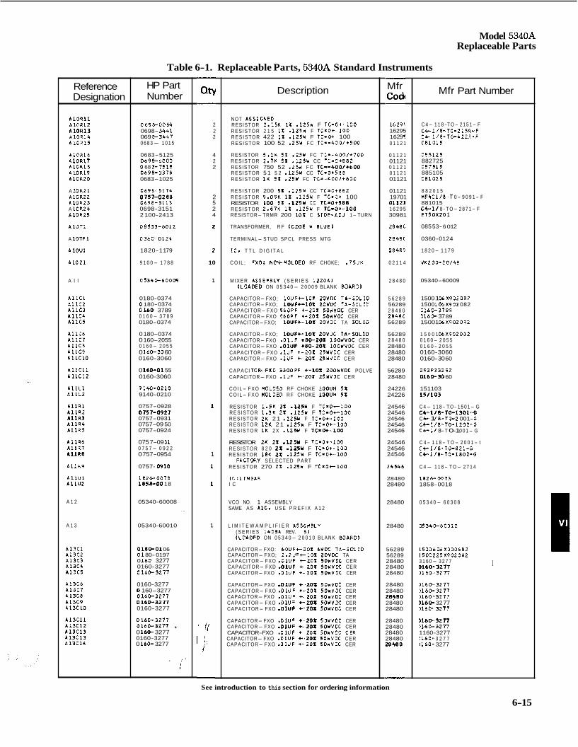
Model 5340A Replaceable Parts
Table 6-1. Replaceable Parts, 5340A Standard Instruments
Reference Designation
A l O R l l A l G R l Z & 1 0 R 1 3 A 1 0 R 1 4 A l O R 1 5
A 1 0 R l 6 A 1 0 R 1 7 A l O R l 8 A 1 0 R 1 9 A l O R 2 0
A 10R21 A l O R Z Z A 1 0 R 2 3 A 1 0 R 2 4 A 1 0 R 2 5
A l O T 1
A l O T P l
A l O U 1
A l O Z l
A l l
A l l C l A l l C Z A l l C 3 A l l C 4 A 1 1 C 5
A l l C 6 A l l C 7 A l l C 8 A l l C 9 A l l C l O
A l l C l l A 1 1 C l 2
A 1 1 L 1 A l l L 2
A I l R 1 A l l R 2 A l l R 3 A l l R 4 A l l R 5
A l l R b A l l R 7 A l l R 8
A l l R 9
A l l U 1 A 1 1 U 2
A 1 2
A 1 3
A 1 3 C 1 A 1 3 C 2 A 1 3 C 3 A 1 3 C 4 A 1 3 C 5
A 1 3 C 6 A 1 3 C 7 A 1 3 C 8 A 1 3 C 9 A 1 3 C 1 0
A 1 3 C l l A 1 3 C 1 2 A 1 3 C 1 3 A 1 3 C 1 3 A 1 3 C 1 4
HP Part Number
0 6 9 8 - 0 0 8 6 0698- 3441 069 8-3447 0 6 8 3- 1 0 1 5
0683-5125 0698-6000 0 68 3-7515 0698-3378 0683-1025
0 6 9 8 - 5 1 7 4 0757-0288 0698-3113 0698-3151 2 100-2413
08553-6012
0360-012*
1820-11 79
9 1 0 0- 1 7 8 8
0 5 3 4 0 - 6 0 0 0 4
0180-0374 0 180- 0374 0 160- 3789 0 1 6 0 - 3 7 8 9 0180-0374
0 180-0374 0 160-2055 0 1 6 0- 2 0 5 5 0 160-30 60 0160-3060
0 160-01 55 0160-3060
9140-0210 9140-0210
0757-0928 0757-0927 0757-0931 0757-09 50 0757-0924
075 7-09 31 0 7 5 7 - 0 9 2 2 0 757-0954
0757- 0910
1826-0073 1858-00 18
05340-60008
05340-60010
0180-01 06 01 80- 0197 0 160- 3277 0160-3277 0160-3277
0160-3277 0 160-3277 0160-3277 0160-3277 0160-3277
0160-3217 0160-3277 9 0 160- 3277 0160-3277 0 160- 3277
. / '
1
- QtY -
2 2 2
4 2 2
2 5 2 4
2
2
10
1
1
1
1
1
1
' li 1 I : -
Description
NOT ASSIGNED RESISTOR 2.15K 1X .125Y F TC=O+- 100 R E S I S T O R 2 1 5 1 X . 1 2 5 U F T C = 0 + - 1 0 0 R E S I S T O R 422 1 X .125W F TC=O+ 100 R E S I S T O R 100 52 .25U F C T C - - 4 0 0 / + 5 0 0
RESISTOR 5.1K 5 1 .25U F C T C = - 4 0 0 / + 7 0 0 R E S I S T O R 2.7K 51 . 1 2 5 Y CC TC=O+882 RESISTOR 750 52 .25Y F C T C - - 4 0 0 / + 6 0 0 R E S I S T O R 5 1 5 2 . 1 2 5 U CC T C - 0 + 5 8 8 R E S I S T O R 1 K 5 1 .25W FC T C - - 4 0 0 / + 6 0 0
R E S I S T O R 200 51: .125W CC TC-O+882 R E S I S T O R 9 .09K 1 X .125U F TC=O+ 100 RESISTOR 100 5 x . 1 2 5 ~ cc T C = O + S ~ ~ R E S I S T O R 2.87K 1 X .125Y F TC=O+-,100 RESISTOR- TRMR 200 102 C S I D E - A O J 1- TURN
TRANSFORMER, R F (COO€ p B L U E 1
TERMINAL- STUD SPCL PRESS MTG
I C r T T L D I G I T A L
C O I L ; FXO; NON-MOLDED R F CHOKE; -75UH
M I X E R ASSEMBLY ( S E R I E S 1 2 2 0 A ) (LOADED ON 0 5 3 4 0- 2 0 0 0 9 BLANK BOAR01
CAPACITOR- FXO; lOUF+-lOX ZOVOC T A - S O L 1 0 CAPACITOR- FXO; l W F + - l O X ZOVDC TA-SOL10 CAPACITOR- FXO 5 6 O P F +-2OX 50WVOC CER CAPACITOR- FXO 5 6 0 P F +-2OX 50WVOC CER CAPACITOR-FXO; l O U F + - l O I ZOVOC TA S O L 1 0
CAPACITOR- FXO; l O U F + - 1 0 2 2OVDC T A - S O L I D CAPACITOR- FXO - 0 l U F +80-2011 lOOWVOC CER CAPACITOR- FXO .01UF +80-201 lOOYVOC CER CAPACITOR- FXO .1UF +-20: 25YVOC CER CAPACITOR- FXO -1UF +-201 25WVOC CER
C A P A C I TOR.-FXD 3 3 0 0 P F +-lo1 2OOYVOC POLVE CAPACITOR- FXO .1UF C 2 0 X 25YVOC CER
C O I L- F X O MOLDED RF CHOKE l O O U H 5 1 C O I L- F X O MOLDED R F CHOKE l O O U H 5X
RESISTOR 1.5K ZX -1ZSW F TC-0 -100 R E S I S T O R 1.3K 2 X - 1 2 5 Y F TC-O+-IOO R E S I S T O R 2 K 2 1 .12% F TC=O+-IOO R E S I S T O R I Z K 2 1 . l 2 5 Y F T C - O + - 1 0 0 R E S I S T O R 1 K 2 X -12% F T C ~ O + = 1 0 0
RESISTOR ZK 21 . iz5n F TC=O+-IOO R E S I S T O R 8 2 0 ZX . l 2 5 Y F TC-O+-100 R E S I S T O R 1 8 K 2 1 . 125Y F TC=O+-*lOO
R E S I S T O R 270 2 X .125W F T C = O t l O O FACTORY SELECTED PART
1C:L INEAR I C
VCO NO. 1 ASSEMBLY SAME A S A 1 0 1 U S E P R E F I X A 1 2
L I M I T E W A M P L I F I E R ASSGMBLV ( S E R I E S 14081 REV. 81 (LOADED ON 0 5 3 4 0- 2 0 0 1 0 BLANK BOAR01
CAPACITOR- FXO: 6 O U F C Z O X 6VDC T A - S M I O CAPACITOR- FXO; 2 . 2 U F t l O X 2OVDC TA CAPACITOR- FXO .01UF t 2 O X 50YVOC CER CAPACITOR- FXD .01UF C 20X 5 0 Y V M : CER CAPACITOR- FXO .OIUF +-ZOX 50UVOC CER
CAPACITOR- FXO - 0 1 U F c 2 0 X 5 0 U V M : CER CAPACITOR- FXO -01UF C 2 O X 5OYVOC CER CAPACITOR- FXO . O W F c 2 O X 50YVOC CER CAPACITOR- FXO .01UF +-2OX 50YVDC CER CAPACITOR- FXO -01UF C Z O X 5OYVOC CER
CAPACITOR- FXO .01UF +-.?OX 50WVOC CER CAPACITOR- FXO -01UF + - 2 O I 5OUVOC CER
CAPACITOR- FXO .O lUF +-2OX 5OWVOC CER CAPACITOR- FXO - 0 l U F +-201 5OYVOC CER
CAPACITOR-FXO .OIUF + 201 5onvoc CER
- Mf r Codc - 16295 16295 16 29 ! 0 1 1 2 1
0 1 1 2 1 01121 0 1 1 2 1 0 1 1 2 1 01121
01121 19701 01121 1 6 2 9 5 30981
2848C
2 8 4 8 C
2848C
0 2 1 1 4
2 8 4 8 0
5 6 2 8 9 56289 2 8 4 8 0
56289
56289 2 8 4 8 0 28480 28480 28480
56289 28480
24226 24226
24546 24546 24546 24546 24546
24546 24546 24546
24546
28480 28480
28480
28480
28480
56289 56289 28480 28480 28480
28480 28480
28480 28480
28480 28480 28480 28480 28480
28?80
-
Mfr Part Number
C 4- 1 1 8 - T O- 2 1 5 1- F C b 1 1 8 - T O - 2 1 5 R - F C 4 - 1 1 8 - T O - 4 2 2 R - F C B 1 0 1 5
C 8 5 1 2 5 882725 C 8 7 5 1 5 885105 C81025
8 8 2 0 1 5 M F 4 C l 1 8 - T 0 - 9 0 9 1 - F 881015 C e l l 8 - T O- 2 8 7 1- F E T 5 O X 2 0 1
085 53- 6 01 2
0360-0124
1 8 2 0 - 1 1 7 9
V K 2 0 0 - 2 0 1 4 8
05340-60009
1500 1 06 X 9 0 2 082 1500 106 X 9 0 2 082 0160-3789 0160- 37 89 15001 0 6 X 9 0 2 0 8 2
1 5 0 0 1 0 6 X 9 0 2 0 8 2 0 1 6 0 - 2 0 5 5 0 1 6 0 - 2 0 5 5 0160-3060 0160- 30 60
2 9 2 P 3 3 2 9 2 0160-30 60
151103 15/103
C 4- 1 1 8- T O- 1 5 0 1- G C b . I / 8 - T O - 1 3 0 1 - G C C 1 18- 1 0 - 2 001- C C 4 - 1 1 8 - T O - 1 2 0 2 - G C4- 1 1 8- T 0-1 0 0 1- G
C 4 - 1 1 8 - T O- 2 0 0 1 - t C 4 - 1 1 8 - T O - 8 2 1 4 C1-118-TO-1802-G
C 4- 1 1 8- T O- 2 7 1 4
1826-0073 1858-0018
0 5 3 4 0- 6 0 3 0 8
05340-60010
1 5 0 0 6 0 6 X 0 0 0 6 8 Z 1 5 0 0 2 2 5 X 9 0 2 0 A 2 3 1 6 0- 3 2 7 7 D160-32TI 1 1 6 0 - 3 2 7 7
3 1 6 0 - 3 2 7 7 1 1 6 0 - 3 2 7 7 1 1 6 0 - 3 2 7 7 1160- 32 77 )160-3277
>160-3277 1160-3277 1160-3277 1160- 3 2 7 7 1160- 3277
I
See introduction to this section for ordering information
6-15
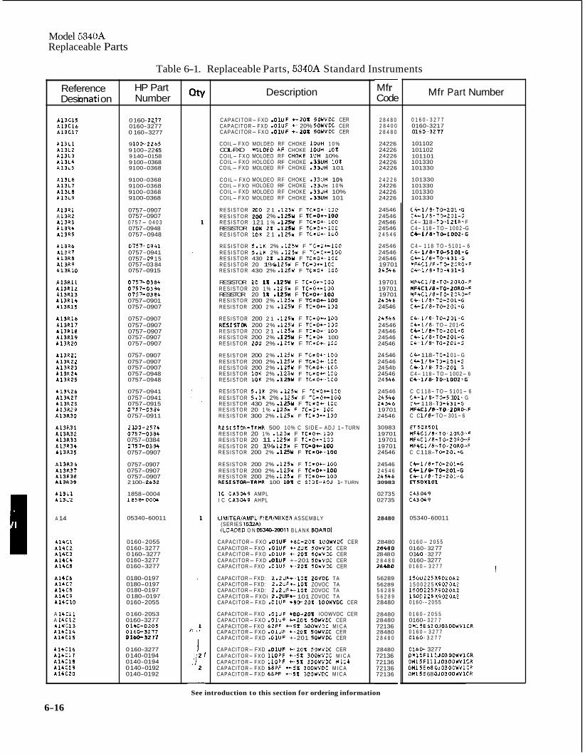
Model 5340A Replaceable Parts
Table 6-1. Replaceable Parts, 5340A Standard Instruments
Reference Desi anati on
A 1 3 C 1 5 A 1 3 C 1 6 A 1 3 C 1 7
A 1 3 L l A 1 3 L 2 A 1 3 L 3 A 1 3 L 4 A 1 3 L 5
A 1 3 L 6 A 1 3 L 7 A 1 3 L 8 A 1 3 L 9
A 1 3 R 1 A 1 3 R Z A 1 3 R 3 A 1 3 R 4 1 1 3 R 5
A l 3 R 6 A 1 3 R 7 A 1 3 R 8 A 1 3 R 9 A 1 3 R 1 0
A 1 3 R l l L 1 3 R 1 2 A 1 3 R 1 3 A 1 3 R 1 4 A 1 3 R 1 5
A l 3 R 1 6 A 1 3 R 1 7 A 1 3 R l 8 A 1 3 R 1 9 A 1 3 R 2 0
A 1 3 R P I A 1 3 R 2 2 A 1 3 R 2 3 A 1 3 R 2 4 A 1 3 R 2 5
A 1 3 1 2 6 A 1 3 1 2 7 A 1 3 1 2 8 A 1 3 R 2 9 A 1 3 R 3 0
A 1 3 R 3 1 A 1 3 R 3 2 A 1 3 R 3 3 A L 3 R 3 4 A 1 3 R 3 5
A l 3 R 3 6 A 1 3 1 3 7 A 1 3 1 3 8 A13R39
A 1 3 U 1 A 1 3 U 2
A 14
A l C C 1 A 1 4 C 2 A 1 4 C 3 A 1 4 C 4 A 1 5 C 5
A l 4 C b A 1 4 C 7 A 1 4 C 8 A 1 4 C 9 A l 4 C l O
A 1 4 C 1 1 A 1 4 C 1 2 A 1 4 C 1 3 A 1 4 C l k A 1 4 C 1 5
A l 4 C l b A 1 4 C 1 7 A l 4 C 1 8 A 1 4 C 1 9 A I 4 C Z O
HP Part Number
0 160- 3277 0160-3277 0 160-3277
9 100-2265 9 100-22 65 9 140-0158 9 100-0368 9100-0368
9100-0368 9100-0368 9100-0368 9100-0368
0757-0907 0757-0907 0 7 5 7- 0 4 0 3 0757-0948 0757-0948
0757=0941 0757-0941 0757- 09 15 0757-03 84 0757-0915
0757-0384 0757-0384 0757-0384 0757-0901 0757-0907
0757-0907 0757-0907 0757-0907 0757-0907 0757-0907
0757- 0907 0757-0907 0757-0907 0757-0948 0757-0948
0757-0941 0757-0941 0757-09 15 0757-0384 0757-0911
2 1 0 0 - 2 5 7 4 0757-0384 0757-0384 0757-0384 0757-0907
0757-0907 0757-0907 0757-0907 2 100- 2632
1858-0004 185&00W
05340-60011
0160-2055 0160-3277 0 160-3277 0160-3277 0160-3277
0180-0197 0180-0197 0180-0197 0 180-0197 0160-2055
0 160-2053 0160-3277 0140-0205 0160-3277 0160-3277
0 160-3277 0 140-0194 0140-0194 0 140-0192 0140-0192
QW Description
CAPACITOR- FXD . D l U F +-20% 50WVOC CER CAPACITOR- FXD .O lUF +- 20% 50YVCC CER CAPACITOR- FXO .O lUF +-20% 50WVDC CER
COIL- FXO MOLDED RF CHOKE l O U H 1 0 %
C O I L- F X O MOLOEO RF CHOKE 1UH 10% COIL- FXO HOLOEO RF CHOKE .33UH 10% COIL- FXD MOLOED RF CHOKE - 3 3 U H 101
COIL-FXO MOLDED RF CHOKE ioun 1 0 %
C O I L- F X O MOLDEO R F CHOKE - 3 3 U H 10% COIL- FXO HOLOEO RF CHOKE .33UH 1 0 % COIL- FXD MOLOEO R F CHOKE .33UH 10% COIL- FXO MOLDED RF CHOKE .33UH 101
R E S I S T O R 200 2 1 .125W F TC=O+-100 R E S I S T O R ZOO 2% .l25W F TC-O+--100 R E S I S T O R 121 1 % - 1 2 5 U F TC=O+-lOO
R E S I S T O R 1 0 K 2 1 -125W F TC=O+-100 RESISTOR ~ O K zx .i25w F TC=O+-IOO
R E S I S T O R 5 . l K 2% .125W F T C - O t 1 0 0 R E S I S T O R 5.1K 2% -125W F T C - O C l O O R E S I S T O R 430 2 1 - 1 2 5 W F TC=0+-100 R E S I S T O R 20 1% -125W F TC-O+-100 R E S I S T O R 430 2% .125U F T C = O + - 1 0 0
RESISTOR 20 1 % .im F ic=o+- ioo R E S I S T O R 20 1 % - 1 2 5 Y F TC=O+-100 RESISTOR 20 1 % .usw F T C = O + - ~ O O R E S I S T O R 200 2% .125W F TC=O+-100 RESISTOR 200 2 % .125W F T C - O c 1 0 0
R E S I S T O R 200 2 1 .125Y F T C * O c l O O RESISTOR 200 2% .125U F T C - 0 + - 1 0 0 R E S I S T O R ZOO 2 1 -125W F TC-Oi -100 R E S I S T O R 200 2% -125Y F TC=O+ 100 R E S I S T O R ZOU 2% d 2 5 U F T C - O C I O O
R E S I S T O R 200 2% .125W F T C = O + - 1 0 0 R E S I S T O R 200 2% .125W F TC=O+-100 R E S I S T O R 200 2% .125Y F TC=O+-100 R E S I S T O R 1 0 K 2% -125W F TC=O+-lOO R E S I S T O R 1 0 K 2% -125U F TC=O+-lOO
R E S I S T O R 5.1K 2% .125u F T C = O c 1 0 0 R E S I S T O R 5.1K 2% .125W F T C - 0 4 - 1 0 0 R E S I S T O R 430 2% .125Y F TC=O+-LOO R E S I S T O R 20 1 % -125W F TC=O+-100 R E S I S T O R 300 2% .125U F TC=0+-100
RESISTOR-7RHR 500 1 0 % C S I D E- A D J 1- TURN R E S I S T O R 20 1 % .125Y F TC-O i -100 R E S I S T O R 20 11 -125W F 7C-O+-100 R E S I S T O R 20 1% .125W F TC=O+-l00 R E S I S T O R 200 2% .125U F TC=O+-100
R E S I S T O R 200 2% - 1 2 5 Y F TC=0+-100 R E S I S T O R 200 2% -125W F TC-O+,100 R E S I S T O R 200 2% . l 2 5 Y F TC-Oi -100 RESISTOR-TRWR 100 10% C S I D E - A D J 1- TURN
I C C A 3 0 4 9 AMPL I C C A 3 0 4 9 AHPL
L IMITER/AMPLIF IER/MIXER ASSEMBLY (SERIES 1532Al ( L O A D E D O N 05340-20011 B L A N K BOARD1
CAPACITOR- FXO -01UF +SO-201 IOOWVDC CER CAPACITOR- FXO -01UF +=to% 5OWVOC CER CAPACITOR- FXO -01UF +-20% 50YVOC CER CAPACITOR- FXD . O W F +-201 50WVOC CER CAPACITOR- FXO -01UF +-20% 5OWVOC CER
CAPACITOR- FXD: 2.2UFC101 ZOVOC TA CAPACITOR- FXD: Z.ZUF+-lO% ZOVOC TA CAPACITOR- FXD: 2.2UF6.101 ZOVOC TA CAPACITOR- FXOi 2.2UF+- 101 ZOVOC TA CAPACITOR- FXD - 0 1 U F +80-201 IOOWVDC CER
CAPACITOR- FXO -0 lUF +80-20% IOOWVDC CER CAPACITOR- FXO .O lUF C Z O I 5OWVOC CER CAPACITOR- FXO 6 2 P F 4-5: 3 0 0 U V D C M I C A CAPACITOR- FXO -0lUF +-ZO% 50WVOC CER CAPACITOR- FXD - 0 1 U F +-201 SOUVDC CER
CAPACITOR- FXD .O lUF +-20% 50WVDC CER CAPACITOR- FXO l l O P F 4-5% 3OOWVDC M I C A CAPACITOR- FXD l l O P F 4-5: 300WVDC M I C A CAPACITOR- FXD 6 8 P F +-5% POOWVOC M I C A CAPACITOR- FXD 6 8 P F +-5% 300YVDC M I C A
- Mf r Code
2 8 4 8 0 2 8 4 0 0 2 8 4 8 0
24226 24226 24226 24226 24226
2 4 2 2 6 24226 24226 24226
24546 24546 24546 24546 2 4 5 4 6
24546 24546 24546 19701 24546
19701 19701 19701 24546 24546
24546 24546 24546 24546 24546
24 546 24546 24 54 b 24546 24 546
24546 24546 24546 19701 24546
30983 19701 19701 19701 24546
24546 2 4 5 4 6 24546 30983
02 73 5 02735
28480
28480 28480 28 48 0 2 8 4 8 0 28480
56289 56289 5 6 2 8 9 5 6 2 8 9 28480
28480 28480 72136 28480 2 8 4 8 0
28480 72136 72136 72136 72136 -
Mfr Part Number
0 1 6 0 - 3 2 7 7 0160-3217 01 6 0 - 3 2 7 7
101102 101102 101101 101330 101330
101330 101330 101330 101330
C 4 - 1 1 8 - 10-201 -G C4-118-TO-201-G C4- 1 18- T 0-1 2 1 R - F C 4- 1 1 8- T O- 1 0 0 2- G C 4 - 1 1 8 * T O - l O O Z - G
C 4 - 1 1 8 T O- 5 1 0 1- 6 C 4 = 1 / 8 - 7 0 - 5 1 0 1 - G C 4 - 1 1 8 - 1 0 - 4 3 1 .G mf4c1 18-TO-ZORO-F C 1 7 1 1 8 - T O - 4 3 1 - G
M F 4 C 1 1 8 - T O - 2 0 R O - F MF4Cl/8=-TO-ZORO-F MF4C118-TO-20RO-F C b l 1 8 - T O - 2 0 1 - G C S - 1 1 8 - T O - 2 0 1 - G
C4-118-TO-ZD1-G C 4 - 1 18- T O- 2 0 1 -G C4-118-TO-201-G C b 1 1 8 - 1 0 - 2 0 1 - G C 4 - 1 1 8 - T O - 2 0 1 - G
C b 118- 10-2 01- G C 4 - 1 1 8 - T O - 2 0 1 - 6 C4-118-TO-201-G C 4- 1 1 8- T O- 1 0 0 2- 6 C b 1 1 8 - T O - l 0 0 2 * G
C C 1 1 8- T O- 5 1 0 1- 6 C 4 - 1 1 8-10-5 1 01- G C4- 118- TO-631-G M F I C I / 8 - T O - Z O R D - F C C 118.. TO- 301- 6
E T 5 0 X 5 0 1 MF4C11B-TO-ZORO-F HF4C 118- T 0-ZORO-F M F 4 C 1 1.9-TO-ZORD-F C C 118- 10-201 -G
C4-118-TO-201-G C C 1 1 8 - T 0 - 2 0 1 - G C4-118-TO-201-G E T 5 0 X 1 0 1
C A 3 0 4 9 C A 3 0 4 9
05340-60011
0 1 6 0- 2 0 5 5 0160- 32 77 01 60- 32 77 0160- 3277 0 1 6 0 - 3 2 7 7 I 1 5 0 0 2 2 5 X 9 0 2 0 A Z 1 5 0 0 2 2 5 X 9 0 2 0 A 2 1 5 0 0 2 2 5 X 9 0 2 0 A 2 1 5 0 0 2 2 5 X 9 0 2 0 A Z 0 1 6 0 - - 2 0 5 5
0 1 6 0 - 2 0 5 5 0160- 3 2 7 7 D H 1 5 E b Z O J 0 3 0 0 W V l C R 0 1 6 0 - 3 2 7 7 0 1 6 0 - 3 2 7 7
0160- 3277 D M l 5 F l l 1 J03OOWVlCR O M 1 5 F l l l J 0 3 0 0 W V l C R D M 1 5 E 6 8 0 J 0 3 0 0 U V l C R OM15E 68 OJ0300WV 1CR
See introduction to this section for ordering information
6-16
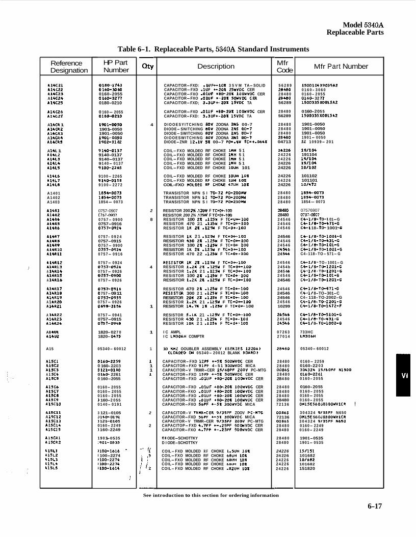
Model 5340A Replaceable Parts
Table 6-1. Replaceable Parts, 5340A Standard Instruments
Reference Designation
A 1 U 2 l A l 4 C 2 2 A14C23 A 1 4 C 2 4 A14C25
A 1 4 t 2 6 A I U 2 7
A 14CR 1 A 1 4 U I 2 A l 4 C R 3 A 14CR4 A14CRS
A 14L 1 A L 4 L 2 A 1 4 L 3 A 1 4 L 4 A 1 4 L 5
A l 4 L 6 A l 4 L 7 A 1 4 L 8
A 1 4 0 1 A 1 4 0 2 A 1 4 0 3
A14R1 A14R2 A l 4 R 4 A14R5 A l 4 R 6
A14R7 A14R8 A14R9 A14R10 A 1 4 R 1 1
A 1 4 R 1 2 A14R13 A 14R14 A14R15 A 1 4 R 1 6
A14R17 A l 4 R 1 8 A l 4 R 1 9 A l 4 R Z O A14R21
A 1 4 R 2 2 A14R23 A14R24
A 1 4 U 1 A14U2
A15
A 1 5 C l A15C2 A l S C 3 A 15C4 A15C5
A15C6 A15C7 A15C8 A15C9 A15C10
A 1 5 C l l A l 5 C 1 2 A15C13 A15C14 A15C15
k 1 5 C R 1 L 151x2
P 1 5 L 1 P 1 5 L 2 P 1 5 L 3 4 1 5 L 4 4 1 5 L 5
HP Part Number
0 1 8 0 = 1 7 4 3 0160-3060 0160-2055
0180-0210
0 160- 2055 0180-0210
1901-0050 190 1- 0050 1901-0050 1 9 0 1 - 0 0 5 0 1 9 0 2 - 3 1 8 2
9 1 4 0 - 0 1 3 7 9140-0137 9140-0137 9 1 4 0- 0 1 3 7 9100-2265
9 1 0 0- 2 2 6 5 9140-0158 9 1 0 0- 2 2 7 2
18540073 1854-0073 1854- 0073
0757-0907 07574907 0 7 5 7- 0 9 0 0 0757-0916 0 1 5 7 - 0 9 2 4
0 7 5 7- 0 9 2 4 0757-0915 0 7 5 7- 0 9 0 0 0 1 5 7 - 0 9 2 4 0 7 5 7- 0 9 1 6
0 7 5 7- 0 9 2 4 0 7 5 1 - 0 9 2 6 0 7 5 7- 0 9 2 6 0757-0900 0 7 5 7- 0 9 2 6
0 7 5 7 - 0 9 1 6 0 757- 09 11 0 7 5 7 - 0 9 5 5 0 7 5 7- 0 9 2 6 0 6 9 6 3 1 5 6
0 7 5 7- 0 9 4 1 0757-0915 0 7 5 7 - 0 9 4 8
1820- 02 7 0 1820- 0 4 7 5
oi60-32n
0 5 3 4 0- 6 0 0 1 2
0 1 6 W 2 2 5 9 0 160- 2203 0121-0180 0 160- 2261 0 160-2055
0 1 6 0- 2 0 5 5 0 1 6 0- 2 0 5 5 0 1 6 0- 2 0 5 5 D 160- 2 0 55 0 1 4 0- 0 1 9 1
3 121-0105 D140-0191 3121-0105 0 1 6 0- 2 2 4 9 3 160-2249
1 9 0 1- 05 3 5 1901-0535
2100-1616 * 3 100-2274 3100-2274 3100-2274 ?loo-1614
I
4
2
8
4
1
1
1
1 1 1 1
2
2
*) ii 1 i3
i -
Description
CAPACITOR-FXD: . l U F i - 1 0 1 3 5 V M TA-SOLID CAPACITOR-FXD -1UF 4-201 ZSYVDC CER CAPACITOR-FXO - 0 1 U F +SO-201 lODYVDC CER CAPACITOR-FXO .01UF + ' 2 O X 5OYVOC C W CAPACITOR-FXD; 3 .3UF+-201 l 5 V O C TA
CAPACITOR-FXD .OlUF i80-201 lOOYVDC CER CAPACITOR-FXD: 3 . 3 U F i - 2 0 1 l 5 V O C TA
D I O O E S Y I T C H I N G 8OV ZOONA 2NS 00-7 DIODE- SNITCHING 8OV ZOONA ZNS 00-7 DIODE-SWITCHING 8OV ZOONA ZNS 00-7 O I O O E S W I T C H I N G 8OV ZOONA ZNS 00-7 DIOOE-ZNR 12.1V 5X 00-7 PoI .4Y T C ~ + . O 6 4 1
COIL-FXO MOLDEO RF CHOKE IMH 5 1 COIL-FXO MOLDED RF CHOKE IMH 5 1 COIL-FXD MOLDED RF CHOKE l M H 5 1 COIL-FXD MOLDED RF CHOKE IMH 5 1 COIL-FXD MOLDED RF CHOKE lOUH 101
COIL-FXD MOLDED RF CHOKE lOUH 101 COIL-FXD MOLDED RF CHOKE I U H 101 COIL-FXO MOLDED RF CHOICE 4 7 ~ ~ i o r
TRANSISTOR NPN S I T O . 7 2 PO=tOOMY TRANSISTOR NPN SI 70-72 P01200MW TRANSISTOR NPN S I 10-72 PO-2DOMY
RESISTOR 200 2% .126W F TC-Ot-100 RESISTOR 200 2% .125W F TC+-100 RESISTOR 100 2 1 .125W F T C * O e 1 0 0 RESISTOR 470 21 .125Y F T C - 0 6 1 0 0 RESISTOR I K 22 .125Y F TC=O+*100
RESISTOR 1 K 2 1 .125Y F T C = O t - l 0 0
RESISTOR 100 2X .125Y F TC=0+-100
RESISTOR 470 22 .125Y F TC*O+-lOO
RESISTOR 430 2% . U ~ Y F ~ c = o t - i o o
RESISTOR IK ZL .i25w F T C = O + - ~ O O
RESISTOR IK 21 .i25n F TC=O+-~OO RESISTOR 1.2K 2 X - 1 2 5 Y F T C = O C l O O RESISTOR 1.2K 2 1 -125W F TC=O*-100 RESISTOR 100 2 X -125Y F TC=O+-100 RESISTOR 1 . 2 ~ 2x .izsn F ~c=o+-ioo
RESISTOR 470 2 X .125W F TC-O+-100 RESISTOA 300 2 1 . l 25Y F TC=Oi-100 RESISTOR ZOK 2x .im F TC=O+-~OO
RESISTOR 14.7~ 11 .125w F TC-O+-~OO
RESISTOR 5.1K 21 -125U F TC-0+100 RESISTOR 430 2 1 .125Y F TC=O+-lOO RESISTOR 10K 2 1 -125W F TC=O+-100
I C AMPL I C LM306H COMPTR
RESISTOR 1.2K 2 1 - 1 2 5 Y F T C * O t l O O
10 MHZ OOUBLER ASSEMBLY ( S E R I E S 1 2 Z O A I (LOADED ON 0 5 3 4 0- 2 0 0 1 2 BLANK BOARD)
CAPACITOR-FXD 12PF +-5% 5OOYVOC CER CAPACITOR-FXO 9 1 P F 4 - 5 1 300UVOC MICA CAPACITOR-V TRMR-CER 1516OPF ZOOV PC-MTG CAPACITOR-FXO 15PF +-52 5OOYVOC CER CAPACITOR-FXO - 0 l U F +80-201 lDOWVDC CER
CAPACITOR-FXO .OlUF +80-201 lOOWVOC CER CAPACITOR-FXO - 0 1 U F +80-201 lOOYVOC CER CAPACITOR-FXO - 0 1 U F +80-201 lOOWVDC CER CAPACITOR-FXD .OlUF i 80 -201 lOOYVOC CER CAPACITOR-FXO 56PF +-51 300UVOC MICA
CAPACITOR-V TRMR-CER 9 / 3 5 P F ZOOV PC-MTG CAPACITOR-FXD 56PF +-51 300WVOC MICA CAPACITOR-V TRMR-CER 9 / 3 5 P F 200V PC-MTG CAPACITOP-FXD 4 . 7 P F +-.25PF SOOWVDC CER CAPACITOR-FXO 4.7PF +-.25PF 5OOWVOC CER
0 1 ODE-SCHOTTKY D I ODE-SCHOTTKY
COIL-FXD MOLDED R F CHOKE 1.5UH 10% COIL-FXO MOLDED RF CHOKE 68UH 101 COIL-FXO MOLDED RF CHOKE 68UH 10% COIL- FXD MOLDED RF CHOKE 68UH 101 COIL- FXD MOLOEO RF CHOKE .8ZUH 101
- Mfr Code
5 6 2 8 9 28480 2 8 4 8 0 28480 56289
2 8 4 8 0 56289
2 8 4 8 0 2 8 4 8 0 2 8 4 8 0 28480 04713
25226 2 4 2 2 6 2 4 2 2 6 24226 24226
24226 2 4 2 2 6 24226
2 8 4 8 0 2 8 4 8 0 2 8 4 8 0
28480 28480 2 4 5 4 6 2 4 5 4 6 2 4 5 4 6
24546 2 4 5 4 6 2 4 5 4 6 24546 24 546
2 4 5 4 6 2 4 5 4 b 24 5 4 6 2 4 5 4 6 24546
2 4 5 4 6 24546 24546 2 4 5 4 6 10299
2 4 5 4 6 2 4 5 4 6 24546
0 7 2 6 3 2 7 0 1 4
2 8 4 8 0
2 8 4 8 0 2 8 4 8 0 0 0 8 6 5 2 8 4 8 0 28 4 8 0
2 8 4 8 0 2 8 4 8 0 2 8 4 8 0 28480 7 2 1 3 6
00865 72136 00865 2 8 4 8 0 2 8 4 8 0
2 8 4 8 0 2 8 4 8 0
24226 24 22 6 2 4 2 2 6 2 4 2 2 6 2 4 2 2 6
-
Mfr Part Number
1 5 0 D l M X 9 0 3 5 A 2 0 1 6 0 - 3 0 6 0 0 1 6 0- 2 0 5 5
1500335XOO15A2
0 160- 2 0 5 5 1 5 0 0 3 3 5 X 0 0 1 5 A 2
1901-0050 1901-0050 1901-0050 1 9 0 1- 0 0 5 0 SZ 1 0 9 3 9- 2 0 1
191104 191104 191104 191104 l01l02
0160- 32 n
101102 101101 io14r2
1 8 5 4 - 0 0 7 3 1854-0073 1854- 0073
07576907 07574007 C 4 1 1 8 - 10-1 01-G C 4 1/8-TO.k71-6 C4- 1 18- T0- 1001 = G
C 4 - 118- 10-1 0 0 1 4 CC1/8-TO-431-G C 4 - 1 / 8 - T 0 - 1 0 l - G C4-118-TO-1001-G C4-118-TO- 571- G
C C 1 1 8 - TO- 1001-G C4- 118- 10-1 2 0 1 - 6 C C - I / 8 - T O - I Z O l - G C4-118- t0-1 01-G C4-118-TO-1201-G
C4-118-TO-571-G C+-l/ 8-TO-301-C C4- 118-TO-2002-G C + l / 8 - T O - I Z O l - G C t l / & T O - l 4 7 2 - F
C4-11.3-TO-5101-G C C l 1 b T 0 - 4 3 1 4 C C 1 1 8- 10-1 002-G
733HC LM306H
0 5 3 4 0- 6 0 0 1 2
0 1 6 0- 2 2 5 9 0160-22 0 3 3 0 4 3 2 4 1516OPF N 1 5 0 0 0160-2261 0 1 6 0- 2 0 5 5
01 60- 20 55 0 1 6 0- 2 0 5 5 0160- 2055 0 1 6 0- 2 0 5 5 OM15E56OJ03DOYVICR ' 1 3 0 4 3 2 4 9 / 3 5 P F N 6 5 0 '
OM15E 56 OJ0300YVlCR 3 0 4 3 2 4 9 / 3 5 P F N 6 5 0 0 1 6 0- 2 2 4 9 0 1 6 0- 2 2 4 9
1901-0535 1 9 0 1- 0 5 3 5
151151 101682 10/682 101682 151820
See introduction to this section for ordering information
6-17
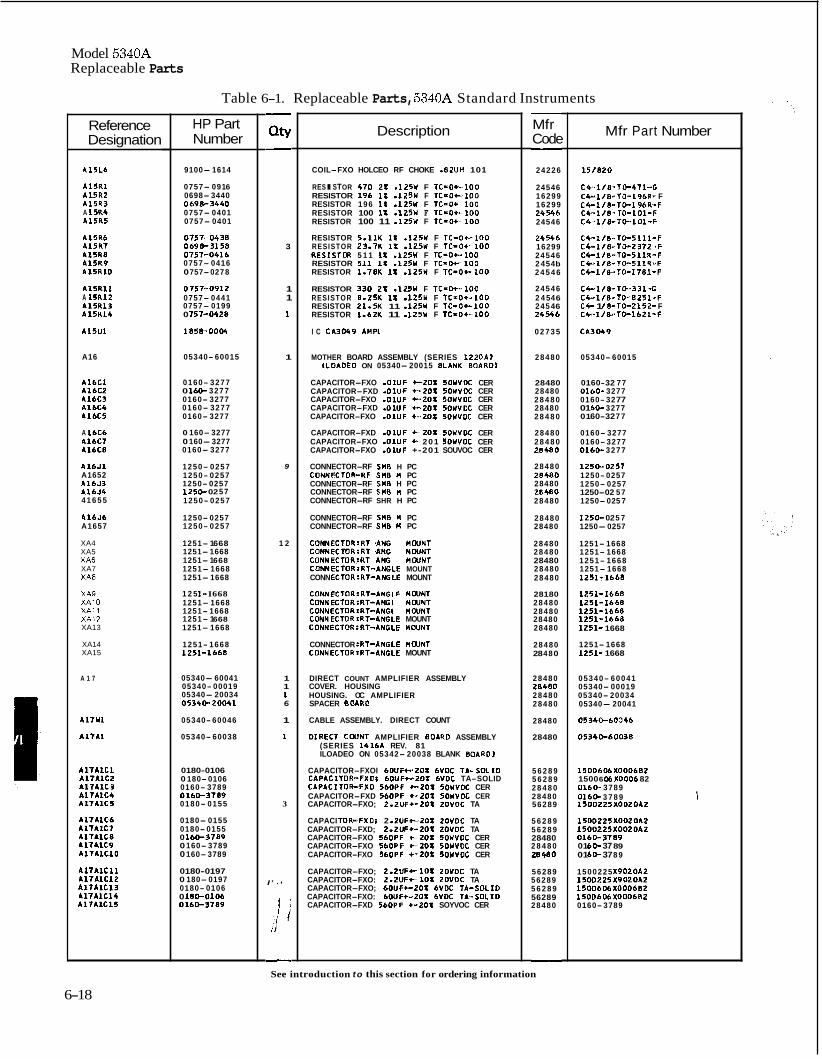
Model 5340A Replaceable Parts
Reference Designation
415L6
A15R1 A15R2 Al5R3 A 15R4 A15R5
A15R6 A15R7 A15R8 A15R9 A15RIO
A15R11 A 1 5 R l 2 A15R13 A15R14
A15U1
A16
AlbC1 Al6C2 A16C3 AlbC4 AlbC5
A 16Cb AlbC7 Al6C8
A l b J 1 A1652 A1653 A1634 4 1 6 5 5
A l 6 J 6 A1657
XA4 XA5 XA6 XA7 XAB
XA9 XAlO XA11 XA12 XA13
XA14 XA15
A 1 7
417W1
A1711
A17AlC1 A17AlC2 A17AlC3 A l7A lC4 A l7A lC5
A l 7 A l C 6 A17AlC7 A17AlC8 A l I A l C 9 A l7A lC lO
A 1 7 A l C l l A l7A lC12 A17AlC13 A l7A lC14 A17AlC15
Table 6-1. Replaceable Parts, 5340A Standard Instruments
HP Part Number
9100- 1614
0757- 091 6 0698- 3440 069E-3440 0757- 0401 0757- 0401
0757- 0438 0698-3158 0757-0416 0757- 0416 0 757-02 78
0757-0912 0757- 0441 0757- 0199 0 757- 0428
1858-,0004
05340- 60015
0160- 3277 0 160- 32 7 7 0160- 3277 0160- 3277 0160- 3277
0 160- 3277 0 160-3277 0160- 3277
1250- 0257 1250- 0257 1250- 0257 1250- 02 57 1250- 0257
1250- 0257 1250- 0257
1251- 1 668 1251- 1668 1251- 1 668 1251- 1668 1251- 1668
1 2 5 1- I668 1251- 1668 1251- 1668 1251- 1 668 1251- 1668
1251- 1668 1251-1668
05340- 60041 05340- 00019 05340- 20034 05340 -20041
05340- 60046
05340- 60038
0180-0106 0 180- 0106 0160- 3789 0160 -3789 0180- 0155
0180- 0155 0180- 0155 0 160-3789 0 160- 3789 0 160- 3789
0180-0197 0 180- 0197 0180- 0106 0 180-0101 0160-3789
- Qw -
3
1 1
1
1
9
1 2
1 1 1 6
1
1
3
I’ , +
i j !i -
Description
COIL-FXO HOLCEO RF CHOKE .82UH 101
RESISTOR 470 2 1 . i 2 5 n F T C - O + - ~ O O RESISTOR 196 i x . i25w F ~ c - o t - i o o RESISTOR 196 1: .125U F TC-O+ 100 RESISTOR 100 11 .125W F TC=O+-100 RESISTOR 100 11 .125U F TC=Ot-100
RESISTOR 5.11K 11 -125U F T C ~ 0 + - 1 0 0 RESISTOR 23.7K 11 .125Y F TC-O+-100 R E S I S T W 5 1 1 11 .125W F TC-O+-100
RESISTOR 1.78K 1 2 .125U F TC-Oi-100 RESISTOR s i i 11 .izsn F TC=O+-~OO
RESISTOR 330 2 1 .im F T C = O + - ~ O O RESISTOR 8-2SK 1X d 2 5 U F TC=O+-lOO RESISTOR 21.5K 11 .125Y F T C - O t l O O RESISTOR 1.62K 11 -125Y F TC=O+-100
I C CA3049 AMP1
MOTHER BOARD ASSEMBLY (SERIES 1220A) (LOADED ON 05340- 20015 8LANK BOAR01
CAPACITOR-FXO .01UF +-201 50YVOC CER CAPACITOR-FXD -01UF +-.?OX 5OWVOC CER CAPACITOR-FXO .OlUF + a 2 0 1 5OUVOC CER CAPACITOR-FXD .OIUF + - to1 50YVDC CER CAPACITOR-FXO -01UF +-2OZ 5OUVOC CER
CAPACITOR-FXD -01UF C ZOX 50WVOC CER CAPACITOR-FXO - 0 I U F +- 2 0 1 5OYVOC CER CAPACITOR-FXO .OlUF +-201 SOUVOC CER
CONNECTOR-RF SM8 H PC CONNFCTOR-RF SH8 H PC CONNECTOR-RF SMB H PC CONNECTOR-RF SMB M PC CONNECTOR-RF SHR H PC
CONNECTOR-RF SM8 M PC CONNECTOR-RF SM8 M PC
CONNECT0R:RT-ANGLE MOUNT CONNECTOR: RT-ANGLE MOUNT CONNECTOR CRT-ANGLE HUJNT CONNECTOR:RT-ANGLE MOUNT CONN ECT0R:RT-ANGLE MOUNT
C0NNECTOR:RT-ANGLE MUJNT . _. CONNECTOR:RT-ANGLE MOUNT CONNECT0R:RT-ANGLE H WNT CONNECT0R:RT-ANGLE MOUNT CONNECTOR:RT-ANGLE MOUNT
CONNECTOR :RT-ANGLE H MINT CONNECT0R:RT-ANGLE MOUNT
DIRECT COUNT AMPLIFIER ASSEMBLY COVER. HOUSING HOUSING. OC AMPLIFIER SPACER BOAR0
CABLE ASSEMBLY. DIRECT COUNT
DIRECT COUNT AMPLIFIER BOAR0 ASSEMBLY (SERIES 1416A REV. 81 ILOADEO ON 05342- 20038 BLANK 8OAROl
CAPACITOR-FXOI 6 O U F C 2 0 1 6VOC TA- SOLID CAPACITOR-FXOI 6 0 U F C Z O I 6VOC TA-SOLID CAPACI7OR-FXO 56OPF +-201 5OUVOC CER CAPACITOR-FXD 56OPF +-ZOX 5OWVDC CER CAPACITOR-FXO; 2.2UF+-2OX ZOVOC TA
CAPACI TOR-FX 0: 2 .ZUF+-ZOZ 2OVOC TA CAPACITOR-FXD; 2.2UF+-201 2OVOC TA CAPACITOR-FXO 56OPF +- 2OI 5OYVOC CER CAPACITOR-FXO 56OPF +-201 50WVDC CER CAPACITOR-FXO 56OPF +-201 5OYVOC CER
CAPACITOR-FXO; 2 . 2 U F r 10: ZOVOC TA CAPACITOR-FXO: 2 . 2 U F t 10X 2OVOC TA CAPACITOR-FXO; bOUF+-ZOI 6VOC TA-SOL10 CAPACITOR-FXO: 60UF+-201 6VOC TA-SOL10 CAPACITOR-FXD 56OPF +-2OX SOYVOC CER
- Mf r Code - 24226
24546 16299 16299 24546 24546
24546 16299 24546 2 4 54 b 2 4 5 4 6
24546 2 4 54 6 24 5 4 6 24546
0 2 7 3 5
28480
28480 28480 2 8 4 8 0 28480 2 8 4 8 0
28480 2 8 4 8 0 28*80
28480 28480 28480 28480 28480
28480 28480
28480 28480 28480 28480 28480
28180 28480 28480 28480 28480
28480 28 48 0
28480 28480 28480 28480
28480
28480
5 6 2 8 9 5 6 2 8 9 2 8 4 8 0 28480 56289
5 6 2 8 9 5 6 2 8 9 28480 2 8 4 8 0 28480
56289 56289 5 6 2 8 9 56289 28480
-
Mfr Part Number
151820
C 4 - 1 1 8 - T 0 - 4 7 1 4 C4-118- 10-1 96R- F C4-118-T0-196R-F C4-118- TO-101-F C4-118-T0-101-F
C4-116-TO-5111-F C b l l 8 . T O - 2 3 7 2 .F C4-118-TO-511R-F C4-118-TO-511R-F C4=118-TO-1781-F
C4-118- TO-3 31 -G C4-118- TO-8251-F C 4 - 1 1 8- 10-2 152- F C4-118-TO-1621-F
CA3049
05340- 60015
0160-32 77 0160- 3277 0160- 32 77 01 60- 3277 01 60-32 7 7
0160- 3277 0160- 3277 0160- 3277
1250 -0257 1250- 0257 1250- 0257 1250-02 57 1250- 02 5 7
1250- 02 5 7 1250- 0257
1251- 1668 1251- 1668 1251- 1668 1251- 1668 1251?1668
1251-1668 1251 -1668 1251 -1668 1251 -1668 1251- 1668
1251- 1668 1251- 1668
05340- 60041 05340- 00019 05340- 20034 05340- 20041
05340-60046
05340-60038
15OObObXOOOb82 1500 6 06 YO006 82 0160- 3789 oibo- 3 7 8 9 \ 1500225X0020A2
1500225XO02OA2 0160-3789 01 6 P 37 89 01 6U- 37 8 9
1500225 X9020AZ 1500225X9020A2 1500606XOOO6BZ 1500606X000682 0160- 3789
See introduction to this section for ordering information
6-18
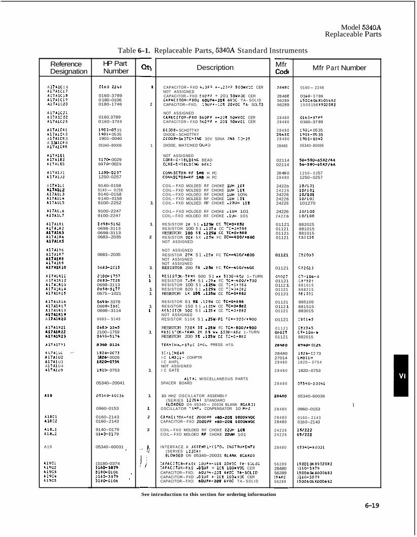
Model 5340A Replaceable Parts
Reference Designation
A 1 7 A l C 1 6 A 1 7 A l C l 7 A 1 7 A l C 1 8 A 1 7 A l C 1 9 A 1 7 A l C Z O
A 1 7 A l C 2 1 A 1 7 A l C Z Z A 1 7 A l C 2 3
A 1 7 A l C R 1 A17ALCRZ A 1 7 A 1 CR 3 A 11 AlCR 4 A 1 7 A l C R 5
A 1 7 A l E I A 1 7 A l E Z A 1 7 A l E 3
A 1 7 A l J l A 1 7 A l J 2
A 1 7 A l L l A 1 7 A l L Z A 1 7 A l L 3 A l 7 A l L 4 A17111L5
A 1 7 A l L 6 A l 7 A l L 7
A 1 7 A l R l A l 7 A l R 2 A 1 7 A l R 3 A 1 7 A l R 4 A 1 7 A l R 5
A l T A l R 6 A 1 7 A l R 7 A l l A l R B A l 7 A l R 9 A 1 7 A l R 1 0
A 1 7 A l R l l A 1 7 A l R 1 2 A l 7 A l R 1 3 A 1 7 A l R 1 4 A l 7 A l R 1 5
A l 7 A L R l 6 A 1 7 A l R 1 7 A 1 7 A l R 1 8 A l l A l R 1 9 A l 7 A l R 2 0
A l 7 A l R 2 1 A 1 7 A l R 2 2 A l T A l R 2 3
A l 7 A l T P 1
A 1 7 1 1 U L . -I
A l 7 A l U 2 A1711 U3 A 17 A 1 U 4 A l l A l U 5
A 1 8
A I 8 C l A 1 8 C 2
A 1 8 L I A I E L Z
A 1 9
h 1 9 C l L 1 9 C 2 A19C3 A 1 9 C 4 A19C5
Table 6-1. Replaceable Parts, 5340A Standard Instruments
HP Part Number
0 1 6 0 - 2 2 4 8
0160-3789 0 180-0106 0180-1746
0160.3789 0 160-37 8 9
1 9 0 1 - 0 5 3 5 1901- 05 35 1901-0040
05340-80006
9170- 0029 9 170- 002 9
1250-0257 1250-0257
9140-0158 9140- 0158 9140-0158 9 140-0158 9100-2252
9100-2247 9100-2247
0698-5180 0698-3113 0698-3113 0683-2035
0683-2035
0683-2015
2100-1757 0183-7525 0698-3113 0698-5111 0675-1021
0690- 3378 0 69 8-3381 0698-3114
0 6 8 3- 5 1 4 5
0683-3345 2100-1759 0698-5174
0360-0124
18260073 1 826- 0026 1820-0154
1820- 0753
05340-20041
05340-60036
0960-0153
0160-2143 0160-2143
9140-0179 9 140-01 79
05340-60031
(3180-0374 )160-3879 0 1 8 0 . 0 1 0 1 , 3 1 6 0 . 3 8 7 9 0 1 8 0 - 0 1 0 6 '
- QQ -
I
2
1
1
1
2
1
1 1
1 1
1 1
1
1
1
1
2
2
" fi
j i -
Description
CAPACITOR- FXD 4.3PF +-.25PF 500WVOC CER NOT ASSIGNED CAPACITOR-FXO 5 6 0 P F + 201 5OWVOC CER CAPACITOR-.FXDi 6OUF+-ZOX 6VOC TA- SOLID CAPACITOR-FXO; l W F + - l O X ZOVOC TA- SOL I0
NOT ASSIGNED CAPACITOR.-FXD 5 6 O P F C Z O X 5OWVOC CER CAPACITOR- FXD 5 6 0 P F +- 201 5OWVCC CER
01 ODE- SCHOTT KY OIOOE-SCHOTTKY DIOOE-SWITCHING 3 0 V 50NA 2NS 00-35
DIODE, MATCHED W A D
NOT ASSIGNED CORE-SHI E L 0 1 NG BEAD CORE-SHIELDING BEAD
CDNNECTOR-RF SH8 H PC CONNECTOR-RF SHE H PC
COIL- FXO MOLDED RF CHOKE 1UH 1 0 X COIL- FXD MOLDED RF CHOKE 1UH '101 COIL- FXO HOLOEO RF CHOKE 1UH 10% COIL- FXO MOLDED RF CHOKE 1UH 1 0 X COIL- FXD MOLDED RF CHOKE - 2 7 U H 10%
COIL- FXD HOLOED RF CHOKE -1UH 101 COIL- FXO HOLOEO RF CHOKE .1UH 101
RESISTOR 2 K 5 1 .125U CC TC-O+882 RESISTOR 100 5 1 -125W CC TC=O+588
RESISTOR 20K 5 X -25W FC T C ~ 4 0 0 / + 8 O O NOT ASSIGNED
RESISTOR loo 5z . izsn cc T C = O + ~ B ~
NOT ASSIGNED RESISTOR 2 0 K 5 1 .25W FC T C ~ - 4 0 0 1 + 8 0 0 NOT ASSIGNED NOT ASSIGNED RESISTOR 200 51 - 2 % F C TC--400/+6GG
RESISTOR-TRHR 500 5 1 W W SIOE-ADJ 1-TURN RESISTOR 7.5K 5 1 .25Y FC TC--400/+700 RESISTOR 100 5 1 .l25W CC TC=0+588 RESISTOR 820 5 1 .125Y CC TC=O+882 RESISTOR IK l o x . i t 5n cc T C = O + ~ ~ Z
RESISTOR 51 5. -12% CC TC=0+588 RESISTOR 150 5 1 - 1 2 5 Y CC TC=O+882 RESISTGR 300 5 1 .125Y CC TC=0+882 NOT ASSIGNED RESISTOR 5 1 0 K 5 1 .25W<FC TC=-800/+900
RESISTOR 3 3 0 ~ 5 1 .t5n FC T C - - ~ O O / + ~ O O
RESISTOR 200 5~ .i25w cc TC-0+882 RESISTOR-TRHR Z K 5 X YW S I O E - A O J 1- TURN
TERWINAL-STUD SPCL PRESS HTG
1C:LINEAR I C L C U l l H COHPTR I C AHPL NOT ASSIGNED I C GATE
A 1 7 A 1 MISCELLANEOUS PARTS SPACER BOARD
10 HHZ OSCILLATOR ASSEMBLY ( S E R I E S l 2 2 0 A J STANOARO (LOADED O h 05340- 20036 BLANK BOARD1
OSCILLATOR TEMP. CONPENSATOR 10 HHZ
CAPACITOR-FXC ZOOOPF +80-201 lOOOYVDC CAPACITOR-FXO ZOOOPF +80-201 lOOOUVOC
COIL- FXO MOLDED RF CHOKE ZZUH 1 O X COIL- FXO MOLOEO RF CHOKE ZZUH 101
INTERFACE A ASSEHBLY(ST0. INSTRUMENTl ( S E R I E S 1 2 2 0 1 1 (LDAOEO ON 05340-20031 BLANK BOARD)
EAPACITOR-FXO: 1 O U F C - l O X ZOVDC TA-SOL10 LAPACITOR-FXD -01UF + 20% lOOYVOC CER CAPACITOR-FXD; 6OUFt -ZOL 6VOC TA-SOL10 CAPACITOR-FXD - 0 l U F +-2OX lOOYVDc CER CAPACITOR-FXO: 60UF+-20X 6VOC T A- S O L I D
- Mfr Codc
2848C
28 48 0 56289 56289
2 8 4 8 0 2 8 4 8 0
2 8 4 8 0
2 8 4 8 0
28480
28480
02114 02114
28 48 0 2 8 4 8 0
2422 b 2 4 2 2 6 24226 24226 24226
24226 2 4 2 2 6
01 121 01121 01121 01121
01121
01121
6 8 0 2 7 01 121 01 12 1 01121 01121
01121 01 12 1 01121
01 121
0 1 1 2 1 6 8 0 2 7 01121
28480
28480 27014 2 8 4 8 0
2 8 4 8 0
2 8 4 8 0
28480
2 8 4 8 0
2 8 4 8 0 28480
2 4 2 2 6 2 4 2 2 6
2 8 4 8 0
5 6 2 8 9 28480 56289 Z8480 5 6 2 8 9 -
Mfr Part Number
0160- 2248
01 60- 3 7 89 1 5 0 0 6 0 6 X 0 0 0 6 4 2 1 5 0 0 1 56 X 9 0 2 0 8 2
0 1 6 0 - 3 7 8 9 01 60-37 89
1901- 05 35 1901-05 35 1901-0040
05340-80006
1 2 5 0 - 0 2 57 1250-0257
10/101 10/101 10/101 10/101 101270
10/100 10/100
882025 881015 881015 C 8 2 0 3 5
C 8 2 0 3 5
C B 2 0 1 5
CT- 106- 4 C 8 7 5 2 5 8 8 1 0 1 5 8 8 8 2 1 5 801021
885105 881515 883015
C 8 5 1 4 5
C 8 3 3 4 5 C T - 1 0 6 - 4 882015
0360- 01 2$
1 8 2 6 0 0 73 L M 3 1 1 H 1 8 2 0- 0 7 5 4
1820-0753
05340-20041
05340-60036
I 0960-0153
0 1 6 0- 2 1 4 3 01 6 0-21 43
15/222 L5/222
D 5 3 4 0 - 6 0 0 3 1
1 5 0 0 1 0 6 X 9 0 2 0 8 2 1160-3879 1 5 0 0 6 0 6 X 0 0 0 6 8 2 1160-3879 1 5 0 0 6 0 6 X O D 0 6 8 2
See introduction to this section for ordering information
6-19
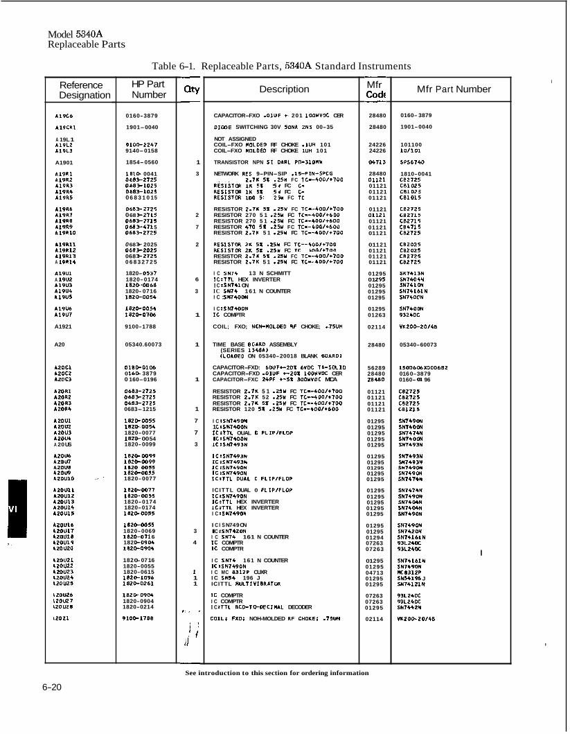
Model 5340A Replaceable Parts
Table 6-1. Replaceable Parts, 5340A Standard Instruments
Reference Designation
A19C6
A19CR1
A 19L 1 A19LZ A19L3
A1901
A19R1 A19R2 A19R3 A19R4 A19RS
A19Rb A19R7 A19R8 A19R9 A19R10
A19Rll A19R12 A19R13 A 196x4
A19U1 A 19UZ A19U3 A19U4 Al9U5
A19W A19U7
A1921
A20
A20Cl A20C2 AtOC3
A2ORl AtOR2 A20R3 A20R4
A2OU1 A2OU2 L20U3 A20U4 A 20 US
A20011 A20U12 A20U13 A20U14 A2OU15
A20U16 IZOU17 A2OUl8 IZOU19 I20U20
nzou21 L20U22 A201123 P20U24 P2OU2S
L20U26 42OLQ7 b2OU28
L2021
HP Part Number
0160-3879
190 1-0040
910-2241 9140-0158
1854-0560
1810- 0041 0683-2725 0 6 8 3 1 0 2 5 0683-1025 0 6 8 3 1 0 1 5
0683-2725 0 68 3-2715 0683- 2715 068 3-471 5 0683-2725
0 68 3 2025 0683-2025 068 3 2 7 2 5 0 6 8 3 2 7 2 5
1820- 0537 1820-0174 1820-0068 1820- 0716 1820-0054
1820-0054 1820-0706
9100-1788
05340.60073
0180.0106 0 16W 3879 0 160-0196
0683-2725 0 6 8 3 2 7 2 5 0683-2725 0683-1215
1820-0055 1 8 Z O - O O H 1820-0077 1820- 00 54 1820- 0099
182G-0099 182WOO99 1820=0055 1820.0055 1820-0077
1820-0077 182*0055 1820-0174 1820-0174 1820-0055
1820-0055 1820-0069 1820-071 6 182 0.0904 1820-0904
182 0- 07 16 1820-0055 1820-0615 1820.1096 1820-0261
182W09O1 1820-0904 1820-0214
9100-1788
- QtY -
1
3
2
7
2
6
3
1
1
1
1
7
7
3
3
4
1 1 1
r , v
t ' ! i
!1
-
Description
CAPACITOR-FXO .OlUF +. 201 lOOWVOC CER
DIODE SWITCHING 30V 50NA 2NS 00-35
NOT ASSIGNED COIL-FXO MOLDED RF CHOKE .lUH 101 COIL-FXO MOLOEO RF CHOKE 1UH 101
TRANSISTOR NPN SI DARL P O = ~ ~ O M Y
RESISTOR 2 . 7 ~ 51 .25w FC T C - ~ O O / + ~ ~ O NETWORK RFS 9-PIN-SIP .lS-PIN-SPCG
RESISTOR 1 K 5% .2SW FC TC=-4001+600 RESISTOR 1K 52 .25U FC TC=-400/+600 RESISTOR 100 s t .25n FC T C = - ~ O O / + S O O
RESISTOR 2 . 7 ~ 51 .25m FC T C - - ~ O O / + ~ O O
RESISTOR 470 5 2 .25w FC T C = - ~ O O ~ + ~ O O
RESISTOR 270 5 1 .25U FC TC--400/+600 RESISTOR 270 5 1 -2% FC TC--400/+600
RESISTOR 2.7K 5 1 .25Y FC TC=-400/+700
RESISTDR 2K 5: -25h FC TC~-400/+700 RESISTOR 2K 5 1 .25n FC TC=-400/+700 RESISTOR 2.711 51 .25m FC T C = - ~ O O / + ~ O O RESISTOR 2.7K 5 1 .25W FC TC-=400/+700
I C SN74 13 N SCHMITT 1C:TTL HEX INVERTER I C : S N74l ON IC SN74 1 6 1 N COUNTER I C : SN7400N
I C :S N7400N IC COMPTR
COIL; FXO; NCN-MOLOEO RF CHOKE; -75UH
TIME BASE BCARD ASSEMBLY (SERIES 13481) (LOADED ON 05340-20018 BLANK BOARD)
CAPACITOR-FXD: 6 O U F t 2 O I bVOC TL-SOLID CAPACITOR-FXD -01UF +-2OI l O O Y V O C CER CAPACITOR-FXC 2 4 ~ ~ +-sz ~ O O W V O C MICA
RESISTOR 2.7K 5 1 .25Y FC TC--400/+700 RESISTOR 2.7K 52 .25H FC TC=-4001+700 RESISTOR 2.TK 5 1 .25W FC TC--4001+700 RESISTOR 120 5 1 - 2 % FC TC=-400/+600
I C ISN7490N 1 C:S N7WON 1C:TTL OUAL D FLIPlFLOP I C:SN7400N lClSN7493N
IC:SN7493N IC:SN7493N I C SN7490N I C :SN7490N 1C:TTL OUAL C FLIPlFLOP
ICITTL OUAL 0 FLIPlFLOP IC:SN7490N 1C:TTL HEX INVERTER 1C:TTL HEX INVERTER I C :S N7490N
I C I S N7 49 ON I C :S N7420N I C SN74 161 N COUNTER 1C COMPTR IC COMPTR
I C SN74 161 N COUNTER I t :SN7490N I C MC 8312P CUXR I C SN54 196 J ICITTL MULTIVIBRATOR
I C COMPTR I C COMPTR I C :TTL 8C0-TO-OECI HAL DECODER
COIL; FXD; NOH-MOLDED RF CHOKE; -75UH
- Mf r Cod€ - 28480
28480
24226 24226
04713
28480 01121 01121 01121 01121
01121 01121 01121 01121 01 121
01 121 01121 01121 01121
01295 01 295 01295 01295 01295
01295 01263
02114
28480
56289 28480 28480
01121 01121 01121 01121
01295 01295 01295 01295 01295
01295 01295 01295 01295 01295
01295 01295 01295 01295 01295
01295 01295 01294 07263 07263
01 295 01295 04713 01295 01295
07263 07263 01295
02114
Mfr Part Number
0160- 3879
1901- 0040
101100 10/101
SPS6740
1810-0041 CP2725 C01025 C8102 5 CBlOlS
C02725 C82715 CB2715 C84715 C82725
C82025 C02025 C82725 C82725
SN7413N SN7404Y SN7410N SN74161N SN74OON
SN7400N 93240C
VKZOO-20148
05340-60073
1500606X300602 016 0-38 79 0160- 01 96
C82725 C82725 C82725 C81215
SN7490N SN140ON SNl474N SN74OON SN7493N
SN7493N SN7493N SN749ON SN7490N SN7474N
SN747kN SN7490N SN74MN SN7404N SN7490N
SN7490N SNl420N SN74161N 93L240C 93L24N.
SN74161N SN7490N HC8312P SN54196 J SN74121N
93L240C 93L240C SN7442N
VK200-20158
I
I
,
See introduction to this section for ordering information
6-20
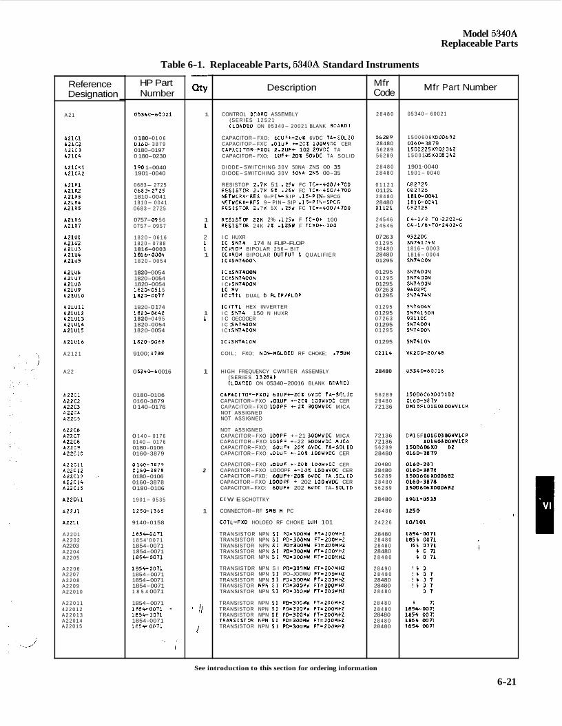
Model 5340A Replaceable Parts
Table 6-1. Replaceable Parts, 5340A Standard Instruments
Reference Designation
A 2 1
A21C1 A21C2 A21C3 A21C4
A Z l C R l A21CR2
A 2 1 R 1 A21R2 A21R3 A 2 1 R 4 A21R5
A21R6 A21R7
A 2 1 U I A21U2 A21U3 A 2 1 U 4 A 2 1 U 5
A21U6 A21U7 A21U8 A 2 1 U 9 A 2 1 U 1 0
A 2 1 U 1 1 A 2 1 U 1 2 A 2 1 U 1 3 A 2 l U 1 4 A 2 1 U 1 5
A 2 1 U 1 6
A 2 1 2 1
A 2 2
A 2 2 C l AZZCZ A22C3 A 2 2 C 4 A 2 2 C 5
AZZC6 AZZC7 A22C8 AZZC9 A 2 2 C 1 0
A Z Z C 1 1 A 2 2 C 1 2 A22C13 .-. A 2 2 C 1 4 A 2 2 C 1 5
A22CR1
A 2 2 J l
A 2 2 L 1
A 2 2 0 1 A 2 2 0 2 A2203 A 2 2 0 4 A 2 2 0 5
A 2 2 0 6 A 2 2 0 7 A 2 2 0 8 A 2 2 0 9 A 2 2 0 1 0
A 2 2 0 1 1 4 2 2 0 1 2 A 2 2 0 1 3 A 2 2 0 1 4 A 2 2 0 1 5
HP Part Number
~
0 5 3 4 6 - 6 0 3 2 1
0 180- 0 1 0 6 O l 6 O 3 8 7 9 0180-0197 0 180-0230
190 1-0040 1901- 0040
0 6 8 3- 2 7 2 5 0 6 8 3 - 2 7 2 5 1810-0041 1 8 1 0- 0 0 4 1 0 6 8 3- 2 7 2 5
0757- 09 5 6 0 7 5 7- 0 9 5 7
1 8 2 0 - 0 6 1 6 1 8 2 0- 0 7 8 8 1816-0003 181b0004 1 8 2 0 - 0 0 5 4
1820- 0054 1820-0054 1820-00 54 1 8 2 0 - 0 5 1 5 1820-0077
1820- 01 74 182&0640 1820- 0 4 9 5 1820-0054 182 0- 0054
1 8 2 0 - 0 0 6 8
9100; 1 7 8 8
0 5340-6 0016
0180-0106 0160-3879 0 140-0176
0 1 4 0- 0 1 7 6 0 1 4 0- 0 1 7 6 0180-0106 0160-3879
0160-3879 0 1 6 0 - 3 8 7 8 0180-0106 0160-3878 0 180-0 106
1 9 0 1- 0 5 3 5
1 2 5 0 - 1 3 6 8
9140-0158
1 8 5 4 - 0 0 7 1 1 8 5 4 ’ 0 0 7 1 1854-0071 18 54-0071 1854-0071
1 8 5 4 - 0 0 7 1 1854-0071 1854-0071 1854-0071 1 8 5 4 0071
1854-0071 1854-0071 1854-0071 1854-0071 18540071
1
1 1
2 1 1 1
1 1
1
2
1
I I/
/ I
Description
CONTROL BOdRO ASSEMBLY ( S E R I E S 1 2 5 2 1 (LOADEO ON 0 5 3 4 0- 2 0 0 2 1 BLANK BOAR01
CAPACITOR-FXO; 6CUF+-ZOI 6VDC 74-SOL10 CAPACITOP-FXC .OlUF CZOI lOOUVOC CER C A P A C I T O R ~ ~ F X O ; 2.2UF+- 102 ZOVOC T A CAPACITOR- FXO; l U F + = 2 0 2 5OVDC T A S O L I D
DIODE- SWITCHING 3 0 V 50NA ZNS 00 35 OIOOE- SWITCHING 3 0 V 5ONA ZNS 00-35
RESISTOP 2.7K 5 1 .25W FC T C - - 4 0 0 / + 7 0 0 PESISTDR 2.7Y 5 Z .25W FC TC=-400/+700 NETYCRK-RES 9-P I N- S I P -15-P IN- SPCG NETWORK-RFS 9- PIN- SIP a15-PIN-SPCG R E S I S T W 2.7K 5X .25W FC T C = - 4 0 0 / + 7 0 0
RESISTCP 2 2 K 2% -12% F TC*O+ 100 R E S I S T M I 2 4 K 22 -125W F TC-O+-100
I C HUXR
1C:ROH BIPOLAR 2 5 6- B I T 1C:ROH BIPOLAR OUTPUT G Q U A L I F I E R I C t S N 7 4 0 0 N
I C :SM4OON I C :SN7400N
IC sm4 174 N FLIP-FLOP
I C IS N 7 4 0 0 N I t HV 1C:TTL DUAL 0 F L I P l F L D P
1C:TTL HEX INVERTER I C S N 7 4 150 N HUXR I C OECOOER I C : S N 7 4 0 0 N I C :S N 7 4 0 0 N
IC:SN7410N
C O I L ; FXO; NDN-HOLDEO RF CHOKE; - 7 5 U H
H I G H FREQUENCY C W N T E R ASSEMBLY ( S E R I E S 1 3 2 8 1 1 (LOADEO ON 05340-20016 BLANK BOARD)
CAPACITOP-FXOi 6 O U F C - 2 0 2 6VOC TA-SOL10 CAPACITOR-FXO .01UF +-201 100WVDC CER CAPACITOR- FXO l O O P F +-22 300WVOC M I C A NOT ASSIGNED NOT ASSIGNED
NOT ASSIGNED CAPACITOR-FXO lOOPF +-21 300WVOC M I C A CAPACITOR- FXO l O O P F +-22 300UVDC M I C A CAPACITOR-FXO; 60UF+ 20% 6VOC TA-SOL10 CAPACITOR-FXO .01UF +-202 lOOWVOC CER
CAPACITOR-FXO - 0 1 U F + . P O X lOOUVOC CER CAPACITOR-FXO LOOOPF +-ZOX lOOYVOC CER CAPACITOR-FXD; 6 O U F + - 2 0 1 6VOC T A . S O L I 0 CAPACITOR-FXO IOOOPF + 202 lOOWVOC CER CAPACITOR-FXO: 60UF+ 202 6VOC TA- S O L I D
01 W E SCHOTTKY
CONNECTOR-RF SHE H PC
COIL-FXD HOLOEO RF CHOKE 1UH 101
TRANSISTOR NPN S I PO-300MW FT-2OOMHZ TRANSISTOR NPN SI PD-300HW FT*ZOOMHZ TRANSISTOR NPN SI PD=300MU FT=ZOI)WPZ TRANSISTOR NPN S I PO=JOOHW FT-200HHL TRANSISTOR NPN 5 1 PO-3OOHW FT-ZOORHL
TRANSISTDR NPN S I PD=330MW FT=20CHHZ TRANSISTOR NPN SI PO-JOOWU FT=ZOOMHZ TRANSISTOR NPN S I PO-300HW FT-ZOOMHZ TRANSISTOR NPN S I P0-300HU FT=ZOOMHZ TRANSISTOR NPN SI PD-300MW FT-ZOOMHL
TRANSISTOR NPN 5 1 PD=3DtHW FT=ZOOWHZ TRANSISTOR NPN SI PD*300HW FT-ZOOHHZ TRANSISTOR NPN S I PO-3OOHW FT=ZOOHHL TRANSISTCIR hPN S I PD-3OOHW FT-ZOOHHZ TRANSISTOR NPN S I P0=300MU FT-ZOOWHZ
Mfr Code
2 8 4 8 0
5 6 2a 9 28480 5 6 2 8 9 5 6 2 8 9
2 8 4 8 0 2 8 4 8 0
0 1 1 2 1 01 12 I 2 8 4 8 0 28480 01121
2 4 5 4 6 2 4 5 4 6
07 26 3 0 1 2 9 5 2 8 4 8 0 28480 01295
01295 0 1 2 9 5 01295 07 26 3 01295
0 1 2 9 5 01295 0 7 2 6 3 01295 0 1 2 9 5
01295
0 2 1 1 4
28480
5 6 2 8 9 2 8 4 8 0 72136
72136 72136 5 6 2 8 9 28480
20480 28480 5 6 2 8 9 2 8 4 8 0 5 6 2 8 9
28480
2 8 4 8 0
2 4 2 2 6
28480 2 8 4 8 0 2 8 4 8 0 28480 2 8 4 8 0
2 8 4 9 0 2 8 4 8 0 28480 28480 2 8 4 8 0
2 8 4 8 0 2 8 4 8 0 28480 2 8 4 8 0 28480
Mfr Part Number
0 5 3 4 0- 6 0 0 2 1
1 5 0 0 6 0 6 Xi300682 0160- 38 79 1 5 0 D Z 2 5 X 9 0 2 0 A Z 1 5 0 0 1 0 5 x 0 0 5 OAZ
1901-0040 1 9 0 1- 0 0 4 0
C B 2 7 2 5 C 8 2 7 2 5 1810-0041 1810-0041 CF!2725
C 4 - 1 1 8 TO-2202-G C 4 . 1 1 8 - T O - 2 4 0 2 - G
9 3 2 2 0 C S N 7 4 1 7 4 N 1 8 1 6- 0 0 0 3 1 8 1 6- 0 0 0 4 SN7400N
SN7400N SN7400N SN7400N 9602PC SN7474N
SN7404N S N 7 4 1 5 0 N 9 3 1 1 0 C SN7400N SN7400N
SN7410N
V K 2 0 0 - 2 0 1 4 8
G 5 3 4 0 - 6 0 0 1 6
1 5 0 0 6 0 6 X 0 0 9 6 8 2
O H 1 5 F 1 0 1 G 0 3 OOWVlCR 0160-3879
O M 1 5F 1 0 1 6 0 3 OOUVlC P OH15F101G0300UV1CR 1 5 0 0 6 0 6 X 0 0 0 6 8 2 0160- 3 8 7 9
0 1 6 0 - 3 8 7 9 01 6 0 - 38 78 1 5 0 0 6 0 6 X 0 0 0 6 8 Z 0160 3878 l 5 0 0 b & X 0 0 0 6 8 2
1901 -05 3 5
1250-1368
101101
i 8 5 4 - o o r i 1854-0071 1 8 5 4 - 0 9 7 1 1 8 5 4 - 0071 1854-0071
1 8 5 4 - 0 0 7 1 1854 0071 1 8 5 4 - 0 6 7 1 1 8 5 4 - 0 0 7 1 1 8 5 4 - 0 0 7 1
1854-0071 1 8 5 4 0071 1 8 5 4 - 0 0 7 1 1854-0071 1 8 5 4 - 0 0 7 1
See introduction to this section for ordering information
6-21
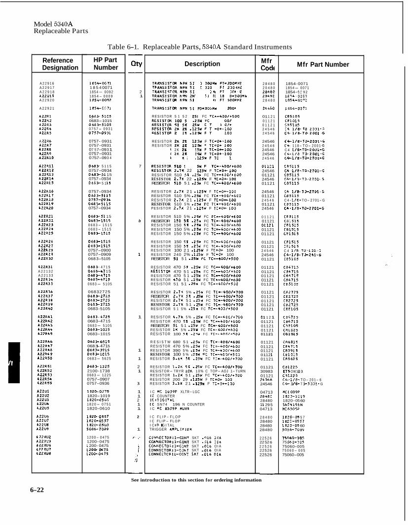
Model 5340A Replaceable Parts
Table 6-1. Replaceable Parts, 5340A Standard Instruments
Reference Designation
A 2 2 9 1 6 A 2 2 9 1 7 A 2 2 9 1 8 A 2 2 9 1 9 A 2 2 9 2 0
A 2 2 9 2 1
A 2 2 R l A 2 2 R 2 A 2 2 R 3 A 2 2 R 4 A Z Z R 5
A 22R6 A 2 2 R 7 A 2 2 1 8 A 2 2 R 9 A 2 2 R 1 0
A 2 2 R 1 1 A Z Z R l 2 A 2 2 R 1 3 A 2 2 R 1 4 A Z Z R 1 5
A 2 2 R 1 6 A 2 2 R 1 7 A 2 2 R 1 8 A 2 2 R 1 9 A22RZO
A 2 2 R 2 1 A 2 2 R 2 2 A 2 2 1 2 3 A 2 2 R 2 4 A 2 2 R 2 5
A 2 2 R 2 6 A 2 2 1 2 7 A 2 2 R 2 8 A 2 2 R 2 9 A Z Z R 3 0
A 2 2 1 3 1 A 2 2 1 3 2 A 2 2 1 3 3 A 2 2 R 3 4 A 2 2 R 3 5
A 2 2 R 3 6 A221137 A 2 2 R 3 8 A 2 2 1 3 9 A 2 2 R 4 O
A 2 2 R 4 1 A 2 2 R 4 2 1221143 A 2 2 R 4 4 A 2 2 R 4 5
A 2 2 R 4 6 A 2 2 R 4 7 A 2 2 R 4 8 A 2 2 R 4 9 A 2 2 1 5 0
A 2 2 1 5 1 A Z Z R 5 2 A 2 2 R 5 3 A 2 2 R 5 4 A 2 2 R 5 5
A Z Z U l A 2 2 U 2 A 2 2 U 3 A 2 2 W A 2 2 U 5
A 2 2 U 6 A 2 2 U 7 A 2 2 U 8 A 2 2 U 9
L 22xu2 A 2 2 X U 3 A 2 2 X U 6 P 2 2 X U 7
HP Part Number
1154-0671 1 8 5 4 0071 1 8 5 4- 0 0 9 2 1 8 5 4- 0 0 0 9 1 8 5 4 - 0 0 9 2
1 8 5 4 - 0 0 7 1
0 6 8 3 - 5 1 0 5 0683-1015 0683-5105 0 7 5 7- 0 9 3 1 0 7 5 7 - 0 9 3 1
0757- 0931 0757-0931 0 7 5 7- 09 3 1 0757-0931 0 757- 09 3 4
0683- 5 1 1 5 0757-09 34 0683-51 15 0757-0934 0683- 5 1 15
0757-0934 0 6 8 3 - 5 1 1 5 0 7 5 7 - 0 9 3 4 0683-5115 0757-0934
0683-51 15 0683-1515 0 6 8 3 - 1 5 1 5 0 6 8 3 - 1 5 1 5 01831515
0 6 8 3 - 1 5 1 5 0 6 8 3 - 1 5 1 5 0757-0900 0757-0909 068 3-5105
0683- 4 7 1 5 0683-47 15 0 6 8 3 4 7 1 5 0683-4715 0 6 8 3- 5 1 0 5
06832725 06832725 0683-2725 06832725 0683-5105
0 6 8 3 . 4 7 2 5 068 3-47 15 0 6 8 3- 5 1 0 5 0 6 8 3 - 1 0 2 5 0683-1015
0 6 8 3 - 6 8 1 5 068 3- 471 5 0 6 8 3 - 3 9 1 5 0 6 8 3 1 0 1 5 0 6 8 3- 5 6 2 5
0683-1225 2100-1738 0 6 8 3- 1 2 2 5 0757-0907 0757-0936
1 8 2 0 - 0 2 7 5 1820-1019 1 8 2 0 - 0 5 6 0 1 8 2 0- 0 7 5 1 1820-0610
1 8 2 0 - 0 5 5 7 1820-0557 1820-0560 5 0 8 6 - 7 0 8 9
1 2 0 0- 0 4 7 5 1200-0475 L 200- 0475 L200=0475 L 2 O D - 0 4 7 5
- Qtv -
2 1
7
b
1
1
1
1
2 1
3
1 1 2 1 1
2
1
t , ,
1 l i
-
Description
TRANSISTOR LPN SI P O = ~ O U M W FT=ZOOMHL T P A N S I STOR h P N S I P n - 3 0 0 Y u FT=ZOOMnL T R A N S I S T @ Q NPN 5 1 TJ-2.1CYY F T = ~ s ) O M H L T R A N S I S T O R h W 2 N 7 0 9 S I T C - 1 8 P D = 3 0 0 Y k TRANSISTOR h P N S I P9-2OOMW FT-600NHL
TRANSISTOR N P h 5 1 P 0 - 3 3 0 Y Y FT-200YWL
R E S I S T O R 5 1 5 2 . 2 5 k FC T C = - 4 0 0 / + 5 O C R E S I S T O R 100 5 1 .25W FC T C = - 4 0 0 / + 5 0 0 R E S I S T O R 5 1 5 % .25W FC T C = - 4 0 0 / + 5 0 0 R E S I S T O R 2 K 2 % .125W F TC=O+ 10J R E S I S T O R 2 K 2% -125W F T C * J * 1 O J
R E S I S T O R 2 K 2 1 - 1 2 % F TC=U+ 100 R E S I S T O R 2 K 22 .125W F TC-0, 100 R E S I S T W . 2 K 2 1 .125W F T C = 0 + - 1 0 0 R E S I S T O R 2 K 2% .125W F T C - O t . 1 0 0 R E S l S T O R 2.7K 21 . 1 2 5 U F T C - O c l O O
RESISTOR 5 1 0 5 % .25Y F C T C - - 4 0 0 / + 6 0 0 RESISTOR 2 . 7 ~ 22 . izsn F ~ t = o + i o o R E S I S T O R 510 5 1 .25W FC T C = - 4 0 0 / + 6 0 0 RESISTOR 2 . 7 ~ 22 .iz5w F T C = O + - ~ O O RESISTOR 510 5 1 .25n FC T C = - ~ O O / + ~ O O
R E S I S T O R 2.7K 2 1 .125W F TC=O+-100 RESISTOR 510 5% .25W F C T C = - 4 0 0 / + 6 0 0 R E S I S T O R 2.7K 2 1 .125W F TC=0+-100 RESISTOR 510 5 % .25W FC T C - - 4 0 0 / + 6 0 0 P E S I S T O R 2.7K 2 1 .125W F TC=04-100
R E S I S T O R 510 5 % -25U FC T C = - 4 0 0 / + 6 0 0
R E S I S T O R 150 5 1 .25W F C T C - - 4 0 0 / + 6 0 0 RESISTOR 150 5 1 -25W FC T C = - ~ O O / + ~ O O
R E S I S T O R 150 5% .ZSW F C T C = - 4 0 0 / + 6 0 0 R E S I S T O R 150 5 % .25W F C T C = - 4 0 0 / + 6 0 0
R E S I S T O R 150 5% .25W FC T C = - 4 0 0 / + 6 0 0 R E S I S T O R 150 5% .25W F C T C - - 4 0 0 / + 6 0 0 R E S I S T O R 100 2 1 .125Y F TC=O+ 100 R E S I S T O R 240 2% -125W F TC=O+ 100 RESISTOR 51 5 1 .25n F C T C = - ~ O O / + ~ O O
R E S I S T O R 470 5 % -25W FC T C = - 4 0 0 / + 6 0 0 RESISTOn 470 5 1 -25W F C T C = - 4 0 0 / + 6 0 0 R E S I S T O R 470 5 1 .25W F C T C = - 4 0 0 / + 6 0 0 R E S I S T O R 470 5 1 - 2 5 Y F C 7 C ~ - 4 0 0 / + 6 0 0 R E S I S T O R 51 5 1 -25W F C T C = - 4 0 0 / + 5 0 0
R E S I S T O R 2.7K 5 % .25W FC 7 C = - 4 0 0 / + 7 0 0
R E S I S T O R 2.7K 5 1 .25U FC T C = - C 0 0 / + 7 0 0 RESISTOR 2.7K 5 1 - 2 5 W F C T C = - 4 0 0 / + 7 0 0 R E S I S T O R 5 1 5 % -25W F C T C = - 4 0 0 / + 5 0 0
RESISTOR t . 7 ~ 5% .ZSW FC T C - - ~ O O / + ~ O O
R E S I S T O R 4.7K 5 % . 2 5 W FC T C - - 4 0 0 / + 7 0 0 R E S I S T O R 470 5 1 -2% FC T C = - 4 0 0 / + 6 0 0
R E S I S T O R 1 K 5 % . 2 5 Y FC T C = - 4 0 0 / + 6 0 0 R E S I S T O R 100 5 1 -25W F C T C - - 4 0 0 1 + 5 0 0
RESISTOR 51 5 1 .25W FC T C = - ~ O O / + ~ O O
R E S I S T W 680 5 1 .25W F C T C ~ - 4 0 0 / + 6 0 0 R E S I S T O R 470 5 % .25W F C T C = - 4 0 0 / + 6 0 0 R E S I S T O R 390 5 % .25W FC T C - 4 0 0 / + 6 0 0 RESISTOR 100 5 % .25Y F C T C - - 4 0 0 / + 5 0 0 R E S I S T O R 5.6K 5 1 .25W FC T C - 4 0 0 / + 7 0 0
R E S I S T O R 1 - 2 K 5 f .25U F C TC-= ,400 /+700 RESISTOR- TRYR 1 0 K 1 0 % C TOP- AOJ 1- TURN R E S I S T O R 1.2K 5 1 .25Y FC T C = - 4 0 0 / + 7 0 0 R E S I S T O R 200 29 -125W F TC-O+-100 R E S I S T O R 3.3K 2 1 -125W F TC=O+-100
I C YC 1 0 3 9 P XLTR-LGC I C COUNTER 1 C : D I G I T A L 1 C S N 7 4 196 N COUNTER I C MC 8 3 0 9 P HUXR
I C F L I P - F L O P I C F L I P- F L O P I C :D I G I T A L TRIGGER P M P L I F I E R
CONNECTORi l -CONT SKT -016 O I A C O N N E C T O R i l - C O N 1 S K T -016 O I A CONNECTORi l -CONT SKT -016 O I A CONNECT0R;l -CONT SKT -016 O I A CONNEC7OR:l-CONT SKT -016 O I A
- Mfr Codf
2 8 4 8 0 2 0 4 8 0 2 8 A 8 C 2 8 4 R 0 2 8 4 8 0
2R48O
01 1 2 1 0 1 1 2 1 0 1 1 2 1 2 4 5 4 6 2 4 5 4 6
24546 2 4 5 4 6 24546 24546 2 4 5 4 6
01121 24546 01121 24546 01121
24546 01121 2 4 5 4 6 01121 24546
0 1 1 2 1 01121 01121 01121 01121
01121 01121 2 4 5 4 6 24546 01121
01121 01121 01121 01121 01121
01121 01121 01 121 01121 01121
01 1 2 1 01121 01121 01121 01121
01121 01121 01121 01 12 1 01121
01121 30983 01121 2 4 5 4 6 24546
0471 3 2 8 4 8 C 28480 01 29 5 04713
2 8 4 8 0 28480 28480 28480
2 2 5 2 6 22 52 6 2 2 5 2 6 22526 22526
-
Mfr Part Number
1854-0071 1 8 5 4- 0 0 7 1 1854- OC 9 2 1 8 5 4 - O O O ? 1 8 5 4 - 0 0 9 2
1 8 5 4 - 0 0 7 1
~ ~ 5 1 0 5 C R 1 0 1 5 C 8 5 1 0 5 c4 i / e - r o 2 0 0 1 - G C 4 - 1 / 8 - T 9 2 0 0 1 ~ G
C 4 - 1 / 8 - T O - Z O O I - G C 4 - 1 1 8- T O- 2 0 0 1 .G C 4 1 / 8 - T O - Z O J l - C C 4 - 1 / 8 T O * Z O O l - G C 4 - 1 / 8 * T O - Z T O l - G
C 8 5 1 1 5 C 4 - 1 / 8 - T O - 2 7 O l - G C 8 5 1 1 5 C 4 - 1 1 8 - T O - 2 7 0 1 - G C 8 5 1 1 5
C 4 1 / 8 - ~ 7 0 - 2 7 0 1 - G C 8 5 1 1 5 C 4 - 118- T O- 2 7 0 1- G C P 5 1 1 5 C 4 - 1 / 8 - T O - 2 7 0 1 - G
C 8 5 l l 5 C 8 1 5 1 5 C 8 1 5 1 5 C B 1 5 1 5 C 8 1 5 1 5
C 8 1 5 1 5 C 8 1 5 1 5 C 4 1 1 8 - T O - 1 0 1 - G C C - l / 8 - T J - 2 4 1 - G C 0 5 1 0 5
C 8 4 7 1 5 C 0 4 7 1 5 C 8 4 7 1 5 C 8 4 7 1 5 C R 5 1 0 5
C R 2 7 2 5 C 6 2 7 2 5 C 8 2 7 2 5 C 8 2 7 2 5 C B 5 1 0 5
C 0 4 7 2 5 C 8 4 7 1 5 C 8 5 1 0 5 C 8 1 0 2 5 C B 1 0 1 5
C 8 6 8 1 5 C 8 4 7 1 5 C 8 3 9 1 5 C B 1 0 1 5 C 8 5 6 2 5
C 8 1 2 2 5 €15 OW1 0 3 C B 1 2 2 5 C4- 118- T O- 2 0 1- 6 C e 1 1 8- T 0-3 3 01; G
M C 1 0 3 9 P 1 8 2 0-1019 1820- 05 60 S N 7 4 1 9 6 N M C 8 3 0 9 P
1 8 2 0 - 0 5 5 7 1 8 2 0 - 0 5 5 7 1 8 2 0 - 0 5 60 5 0 0 6 - 7 0 8 9
75n60-00s 75 060-005 75060-005 7 5 0 6 0 - 0 0 5 75060-005
See introduction to this section for ordering information
6-22
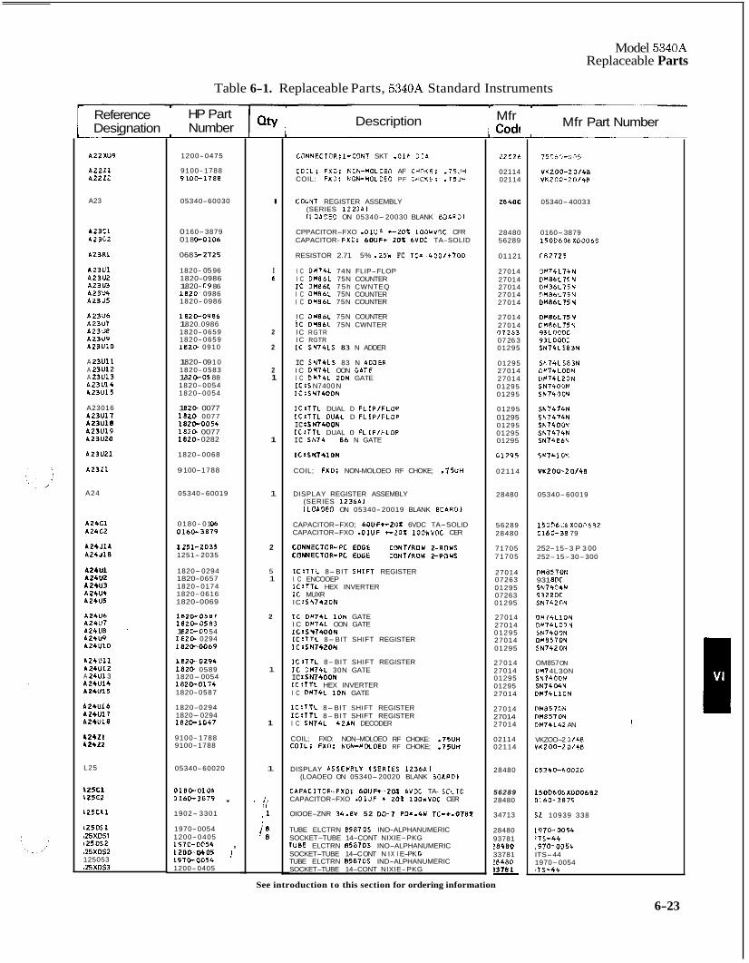
Model 5340A Replaceable Parts
Reference Designation
A22XU9
A22.?1 A2222
A23
A23C1 A23C2
A23R1
L23U1 A23UZ A23U3 A23U4 A23U5
A23U6 A23U7 A23U8 A23U9 A23U10
A 23U11 A 23U12 A 23U13 A23Ul4 A23U15
A23016 A23U17
A23U19 A23UZO
a 2 3 u i e
A231121
A2321
A24
A24C1 A24C2
A24JlA A24J18
A24U4 424U5
A24Ub A24U7 A24U8 '
AZ4W A24U10
A 2 4 U l l A24U12 A 2401 3 A24U14 A24U15
A24U16 A24U17 A24Ul8
L25
\25C1 h25C2
L25CRl
L250S1 Q5XOS1 L25DS2 25XDS2 125053 125XDS3
Table 6-1. Replaceable Parts, 5340A Standard Instruments
HP Part Number
1200- 0475
9100-1788 9100-1788
05340-60030
0 160-3879 0 1 8 0-0106
068 3-2725
1820- 05 96 1820-0986 1 820- C 9 86 1 8 2 e 0986 1820- 0986
1820.0986 1 820.0986 1820- 0659 1820- 0659 1820- 0910
1 820- 09 1 0 1820- 0583 1 820-05 88 1820- 0054 1820-0054
1 82D- 0077 1820- 0077 1820-0054 1820; 0077 1820.- 0282
1820- 0068
9 100- 1788
05340-60019
0 180- 01 06 0 1 6 S 3 8 7 9
1251-2035 1251-2035
1820- 0294 1820- 0657 1820- 0174 1820- 0616 1820-0069
1820-0587 1820-0583 1 8 2 0 0 0 54 1820- 0294 1820-0069
1820-0294 1820- 0589 1820- 0054 1820-0174 1820- 0587
1820- 0294 1820-0294 1820-1047
9100- 1788 9100-1788
05340-60020
0180-0106 Dl60-3879 ,
1902- 3301
1970-0054 1200- 0405 197@-0054 , 120(bW05 1 1970-0054 1200-0405
I
I 6
2
2
2 1
1
1
2
5 1
2
1
1
1
t /I 41 I f
Description
CONNECTOR;l-CflNT SKT .016 DIP
COIL: FXD; LCN-MOLOEO AF CHnKE; .75UH COIL: FXO: NON-MOLDED PF CHOKF: .75UH
COUNT REGISTER ASSEMBLY (SERIES 1220A1 (LOAOEO ON 05340- 20030 BLANK BOARD1
CPPACITOR-FXO - 0 l U F +-20t lOOUVOC CFR CAPACITOR- FXD; 6OUF+-ZOt 6VOC TA-SOLID
RESISTOR 2.71 5% .25U FC TC=-400/+700
I C OM74L 74N FLIP-FLOP I C OM86L 75N COUNTER I C DM86L 7 5 h CWNTEQ I C OYR6L 75N COUNTER I C OM86L 75N COUNTER
I C DM86L 75N COUNTER IC D W 6 L 75N CWNTER I C RGTR I C RGTR 1C S M 4 L S 83 N ADDER
IC SN74LS 83 N AODER I C OM74L OON GATF I C OM74L ZON GATE 1 C :S N7 400 N IC:SN7400N
1C:TTL DUAL D FLIPlFLOP ICXTTL DUAL D FLIPlFLOP IC :SN7400N 1C:TTL DUAL 0 FLIP/FLOP IC SN74 86 N GATE
IC:SU7410N
COIL; FXO; NON-MOLOEO RF CHOKE; .75UH
DISPLAY REGISTER ASSEMBLY (SERIES 123641 ILOAOEO ON 05340-20019 BLANK BOAR01
CAPACITOR-FXO; 6OUF+-20% 6VDC TA-SOLID CAPACITOR-FXO -010F C Z O X lOOWVOC CER
CONNECTOR-PC EOCE 15-CONTIRDW 2-ROWS CONNECTOR-PC EOCE 15-CONTIROW 2-POUS
1C:TTL 8-BIT SHIFT REGISTER I C ENCOOEP ICXTTL HEX INVERTER IC MUXR I C :SN7420N
IC DM74L lON GATE I C OM74L OON GATE IC:SN7400N 1C:TTL 8- BIT SHIFT REGISTER I C zSN7420N
1C:TTL 8-BIT SHIFT REGISTER I t OM74L 30N GATE IC :SW400N 1C:TTL HEX INVERTER I C OM74L ION GATE
1C:TTL 8-BIT SHIFT REGISTER I C I T T L 8- BIT SHIFT REGISTER I C SN74L 42bN DECODER
COIL; FXO: NON-MOLOEO RF CHOKE: .75UH COIL; FXO; NGN-MDLOEO RF CHOKE; .75UH
DISPLAY ASSEYBLY (SERIES 1236A1 (LOAOEO ON 05340-20020 BLANK BOARD1
CAPACITOR-FXOi 60UF+-.20% 6VOC TA- SDLID CAPACITOR-FXO -01UF + 202 lOOUVOC CER
OIOOE-ZNR 34.8V 52 00-7 P0=.4W TC=+-078T
TUBE ELCTRN 858705 INO-ALPHANUMERIC SOCKET-TUBE 14-CONT NIXIE-PKG rU8E ELCTRN B5870S INO-ALPHANUMERIC SOCKET-TUBE 14-C ONT N I X I E-PK G TUBE ELCTRN 858705 IND-ALPHANUMERIC SOCKET-TUBE 14-CONT NIXIE-PKG
Mfr Codc
2252t
02114 02114
2848C
28480 56289
01121
27014 27014 27014 27014 27014
27014 27014
07 26 3 01295
01295 27014 27014 01295 01295
01295 01295 01295 01295 01295
(11295
02114
07263
28480
56289 28480
71705 71705
27014 07263 01295 07263 01295
27014 27014 01295 27014 01295
27014 27014 01295 01295 27014
27014 27014 27014
02114 02114
28480
56289 28480
34713
28480 93781
33781 !8480
~ ~ 8 0
-
Mfr Part Number
7506'!-9'5
v ~ 2 0 0 - 2 0 / 4 a VK200-20140
05340-4003 3
0160-3879 150D606X00066
C82725
OM74L74N DM86L75N OMSbL75N DM86L75N OH86L75Y
DPl86L75N DM86L75N 93LOODC 93LOODC SN74LS83N
SN74LS83N DM74LOON OH74L20N SN7400N SN7400Y
SN7474N SN7474N SN7400N SN7474N SN7486N
SN7410N
05340-60019
150D6Ob XOOP642 0160-38 79
252- 15- 3 P 3 00 252-15-30-300
@M8570N 931 8DC SN7404N 9322DC SN742nN
OM74L10N DM74LOir Y SN7400N OM8570N SN7420N
OM857 ON OM7 4L 3 0 N SN7400N SNI404N OM74LlON
DH8570N DM8570N OM74L42 AN I VKZOO-2 3/48 VK2OO-2 0148
05340-60022
150D606XOOO6B2 D160-3879
SZ 10939 338
L970-Do54 1TS-44 1910-0054 ITS-44 1970-0054 ;TS-44
See introduction to this section for ordering information
6-23
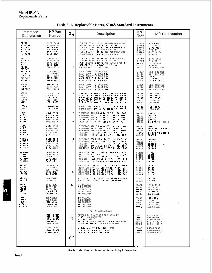
Model 5340A Replaceable Parts
Table 6-1. Replaceable Parts, 5340A Standard Instruments
Reference Designation
A 2 5 0 S 4 A25XDS4 A 2 5 0 5 5 A25XDS5 A25DSb A25XDS6
A 2 5 0 S 7 A25XOS7 A 2 5 0 5 8 A25XOSB A 2 5 0 5 9 A25XOSQ A 2 5 0 S 1 0 A 2 5 0 5 1 1 A 2 5 0 S 1 2 A 2 5 0 5 1 3 A 2 5 0 S 1 4
A 2 5 0 5 1 5 A 2 5 0 5 1 6 A 250s 17
A 2 5 9 1 A 2 5 9 2 A 2 5 9 3 A 2 5 9 4 A25Q5
A 2 5 9 6 A 2 5 9 7
A 2 5 R 1 A25R2 A 2 5 R 3 A25R4 A25R5
A25R6 A 2 5 R 7 AZSR8 A 2 5 R 9 A 2 5 R 1 0
A 2 5 R l l A 2 5 R 1 2 A 2 5 1 1 3 A 2 5 R 1 4 A 2 5 R 1 5
A 2 5 R 1 6 A 2 5 R 1 7 A 2 5 R l 8 A 2 5 1 1 9 A 2 5 1 2 0
A 2 5 R 2 1 A 2 5 R 2 2 A 2 5 1 2 3 A 2 5 R 2 4 A 2 5 R Z 5
A25RZb A 2 5 R 2 7
A 2 5 U 1 A 2 5 U 2 A 2 5 U 3 A 2 5 M A25U5
A25116 A 2 5 U 7 A25U8 A 2 5 0 9 A 2 5 U 1 0
HP Part Number
1 9 7 0- 0 0 5 4 1 2 0 0- 0 4 0 5 1 9 7 0 - 0 0 5 4 1200-0405
1970-00 5 4 1 2 0 0 - 0 4 0 5 1970-0054 1200- 0405 2 1 4 0- 0 3 1 3
2140-0313 2140-0313 2 1 4 0- 0 3 1 3 214W 03 13 2 140- 03 13
2140-C313 2 140-0313 2 140- 0313
1 8 5 4- 0 5 3 3 1 8 5 4- 0 5 3 3 1 8 5 4 - 0 5 3 3 1854- 0533 1 8 5 6 0 5 3 3
1854-0533 1 8 5 4 - 0 0 7 1
0083-4735 0683-4735 0 6 8 3 4 7 3 5 0 683-4735 0757-05'43
018 3 4 7 3 5 0 7 5 7- 0 9 4 3 0 68 3- 4 7 3 5 0 7 5 7- 0 9 4 3 0 6 8 3 - 4 7 3 5
0683-2045 0 683-2735 0683-2725 0683-2735 0683- 2 7 2 5
0683- 2735 0683-2725 0 68 3- 273 5 0683-2725 0 6 8 3 - 2 7 3 5
0 6 8 3- 2 7 2 5 0 6 8 3 - 2 7 3 5 0 6 8 3- 2 7 2 5 0 68 F 2 4 2 5 0683-2725
0683- 5125 0683-2735
1820-11 61 1820-1161 1820-1161 1 8 2 C L 1161 1 8 2 0 - 1 1 6 1
1820- 11 61 1820-1161 18201161 1 8 2 0 - 1 1 6 1 1 8 2 0 - 1 1 61
0 5 3 3 0 00027 0 5 3 3 0 - 4 0 0 0 2 0 5 3 4 0 00006 5534C-00007 3 5 3 4 0- 6 0 0 5 7
0 5 3 4 0- 8 0 0 0 1 0 53kO-80002 D 5 3 S O - 8 0 0 0 3
QtY
9
12
7
9
1 8
1
10
1 3 1 1 1
l i '1
i ;i
Description
TUBE ELCTRN 8 5 8 7 0 5 INO-ALPHANUMERIC SOCKET-TUBE 14-C ON1 N I X l E -PKG TUBE FLCTRN 8 5 8 7 0 5 IND-ALPHANUMEl3IC SOCKET-TUBE 14-CON1 N I X I E- P K G TUBE FLCTRh 8 5 8 7 0 s IND-ALPHANUMERIC SCCKET-TUBE 14-CON1 N I X I E- P K G
TUBE ELCTRN 858705 IND-ALPHANUMERIC S OCK ET -TU 8 E 14- CON T N I X I E-PK G TUBE ELCTRN 858705 INO-ALPHANUMER TC S O C K E T ~ T U B E GCONT N I x I E-PKG LAUP-GLOW 1-2 BULB 58V
LAMP-GLOW T- 2 BULB 58V LAUP-GLOW 1-2 BULB 58V LAMP-GLOW T- 2 BULB 5 8 V LAMP-,GLOW T,-2 BULB 58V LAMP-GLOW 1-2 BULB 5 8 V
CAMP-GLOW 1-2 BULB 58V LAUP-GLOW T-2 BULB 5 8 V LAMP-GLOW 1-2 BULB 5 8 V
TRANSISTOR h P N S I PO-625MW FT-lOOUHZ TRANSISTOR h P # SI PO-625UW FT-lOOMHL TRANSISTCR NPN SI ~ o - 6 2 5 ~ ~ FT-ICOMP~
'TRANSISTOR NPN S I PO-625NU FT-lOOPlHZ TPANSISTOR NPN SI PO-625MW FT-10OUHZ
TRANSISTOR NPN S I PO-625MW FT=lOOMHZ TRANSISTOR N P h SI P0-30OMU F T - 2 0 0 M H I
RESISTOR 4 7 K 5 1 .25W FC TC=-400/+800 RESISTOR 4 7 K 5 % .25W FC TC=-400/+800 RESISTOR 4 7 K 5X .25W FC TC--400/+800 RESlSTOR 4 7 K 51 -25W F C TC=-400/+800 RESISTOR 6 . 2 ~ ti . i z w F T C - O ~ ~ O O
RESISTOR 4 7 K 5 1 .25W FC TC=-400/+800 RESISTOR 6.2K 2% -125W F T C - O c l O O RESISTOR 4 7 K 5 1 -25W. FC TC--400/+800 RESISTOR 6.2K 2% .125W F T C - O c 1 0 0 RESISTOR 4 7 K 5 X - 2 % F C TC*-400/+800
RESISTOR 200K 5 1 .25W FC TC=-800/+900 RESISTOR 2 7 K 5% .25U FC TC--400/+800 RESISTOR 2.7K 5% .25W FC T C - - 4 0 0 / + 7 0 0 '
RESISTOR 2 7 K 5 1 -2% FC TC--400/+800 RESISTOR 2 . 7 ~ 5 1 .BY FC T C - - ~ O O / + ~ O O
RESISTOR 2 7 K 5% -25W FC TC--400/+800 RESISTOR 2.7K 5 1 .25W FC TC=-400/+700 P E S I S T O R 2 7 K 52 .25W F C T C - - 4 0 0 / + 8 0 0 RESISTOR 2.7K 5% .25W FC T C - - 4 0 0 / + 7 0 0 RESISTOR 2 7 K 5% - 2 % F C TC--600/+800
RESISTOR 2-71: 5% .25Y FC T C = - 4 0 0 / + 7 0 0 RESISTOR 2 7 K 5 1 -25W F C TC--400/+800 RESISTOR 2.7K 5 1 .25U FC TC=-400/+700 RESISTOR 2.4K 5 1 .25Y FC T C = - 4 0 0 / + 7 0 0 RESISTOR 2.7K 5% -2SW FC TC--400/+700
RESISTOR 5 . 1 K 5% .25W FC TC=-400/+700 R E S I S T O R 2 7 K 52 .25W FC TC=400 /+800
I C DECODER IC DECODER I C DECODER I C DECODER IC OECCOER
IC OECOOER IC DECODER I C DECODER I t DECODER IC DECODER
A 2 5 MISCELLANEOUS
RETAINER. R I G H T ( S I N G L E BRACKET) BLOC K. ANNUNCIATOR S H I E L O t N I X I E BRACKETS ANNUNCIATOR (DOUBLE BRACKET) CABLE ASSEIIBLYI D I S P L A Y BLANKING
INOICATORv OF Lot LOCK, GATE INOXCATOR. GHZI MHZ. KHZ I N D I C A T O R * RCTI D I R . ~l~
- Mfr Codr
2 8 4 8 0 8 3 7 8 1 28480 8 3 7 8 1 28480 8 3 7 8 1
284RO 8 3 7 8 1 28480
7 4 2 7 6
74 27 6 7 4 2 7 6 74276 74276 7 4 2 7 6
74276 74276 7 4 2 7 6
28480 28480 2 8 4 8 C 28480 28480
2 8 4 8 C 2 8 4 8 0
01121 01121 01121 01121 24546
01121 24546 01121 2 4 5 4 6 01121
01 121 01121 01121 01121 01121
01121 01121 01121 01121 01121
01121 01121 01121 01121 01 12 1
01121 01121
28480 2 8 4 8 0
8 3 7 ~ 1
ZWRO 2 8 4 ~ 0 28480
28480 2 8 4 8 0 28480 28480 2e4so
2 8 4 8 0
28480 2 8 4 8 0 28480
28480 28480 2 8 4 8 0
28480
-
Mfr Part Number
1 9 7 0 - @ 0 5 4 R T S- 4 4 1 9 7 0 - 0 0 5 + RTS- 44 1 9 7 0- 0 0 5 4 RTS- 44
1 9 7 0 - 0 0 5 5 P TS- 44 1 9 7 0 - 0 0 5 4 RTS- 44 NCZH FROSTED
NEZH FROSTED NEZH FROSTED NEZH F90STEO NEZH FROSTEO hE2H FROSTED
NEZH FROSTED NEZH FROSTFO NEZH FROSTED
1 8 5 4- 0 5 3 3 1 8 5 4 - 0 5 3 3 1 8 5 4 - 2 5 3 3 1 8 5 4- 0 5 3 3 1854-0533
1 8 5 4 - C 5 3 3 1854-0071
C 8 4 7 3 5 C R 4 7 3 5 C 8 4 7 3 5 C 8 4 7 3 5 C4-118- TO-6 201- G
C 8 4 7 3 5 C4-1 /8=TO-b201-G C 8 4 7 3 5 C & l / 8 - T O - 6 2 0 1 - G C 8 4 7 3 5
C B 2 0 4 5 C B 2 7 3 5
C B 2 7 3 5 C 8 2 7 2 5 C 8 2 7 3 5 C 8 2 7 2 5 C 8 2 7 3 5
C 8 2 7 2 5 C B 2 7 3 5 C 8 2 7 2 5 C 8 2 4 2 5 C B 2 7 2 4
C 8 5 1 2 5 C 8 2 7 3 5
1 8 2 0 - 1 1 6 1 1820-1161 1820-1161 182 0-1161 1 82 0-1 161
1820- i i 61 1820-1161 1 8 2 0 - 1 1 61 1 8 2 0 - 1 1 6 1 1820-1161
0 5 3 3 0- 0 0 0 2 7 05330-40002 0 5 3 4 0- 0 0 0 0 6 0 5 3 4 0 - 0 0 9 0 7 0 5 3 4 0- 6 0 0 5 7
05340-80001 05340-80002 05340-80003
See introduction to this section for ordering information
6-24
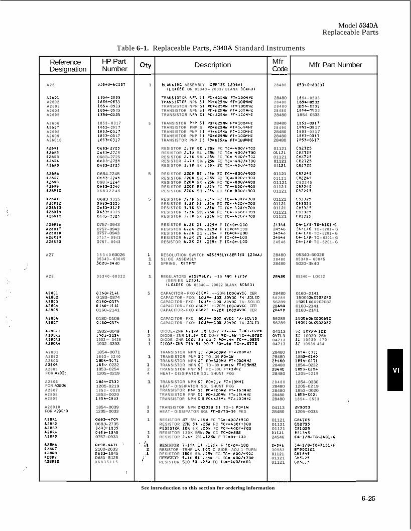
Model 5340A Replaceable Parts
Reference Designation
A 2 6
A 2 6 0 1 A 2 6 0 2 A 2 6 9 3 A 2 6 0 4 A 2 6 9 5
A 2 6 0 6 A 2 6 0 7 A 2 6 9 8 A 2 6 0 9 A 2 6 0 1 0
A Z b R 1 A 2 6 R 2 A 2 6 R 3 A 2 6 R 4 A 2 6 R 5
A 2 b R 6 A 2 6 R 7 A 2 6 R 8 A 2 6 R 9 A 2 6 R 1 0
A 2 6 R l l A 2 6 R 1 2 A 2 6 R 1 3 A 2 6 1 1 4 A 2 6 R 1 5
A 2 6 R 1 6 A 2 6 R l 7 A 2 b R 1 8 A 2 b R 1 9 A 2 6 R 2 0
A 27
A 2 8
A 2 8 C l A 2 8 C 2 A 2 8 C 3 A 2 8 C 4 A 2 8 C 5
A 2 8 C 6 A Z 8 C 7
A 2 8 C R l AZBCRZ A 2 8 C R 3 A 2 8 C R 4
A 2 8 0 1 A 2 8 9 2 A 2 8 0 3 A 2 8 0 4 A 2 8 0 5 FOR ~ z 8 a 5
FOR A Z ~ A 2 8 0 6
A 2 8 0 7 A 2 8 0 8 A 2 8 0 9
A 2 8 0 1 0 FOR A28010
A 2 8 R l A 2 8 R 2 A 2 8 R 3 A 2 8 R 4 L 2 8 R 5
L28R6 4 2 8 R 7 L28R8 L Z 8 R 9 928R10
Table 6-1. Replaceable Parts, 5340A Standard Instruments
HP Part Number
05340-66037
1 8 5 4 - 0 5 3 3 1 8 5 4 - C 5 3 3 1 8 5 4 - 0 5 3 3 1 8 5 4 - 0 5 3 3 1 8 5 4 0 5 3 3
1 8 5 3 - 0 3 1 7 1 8 5 3 - 0 3 1 7 1853-0311 1 8 5 3 - 0 3 1 7 1853-0317
0683-2725 0 6 8 3 2 7 2 5 068 3- 27 25 0683-2725 0 6 8 3 - 2 7 2 5
0 684.2245 0 6 8 3 - 2 2 4 5 068 f 2 2 4 5 0683-2245 0 6 8 3 2 2 4 5
0683 3 3 2 5 0 6 8 3 - 3 3 2 5 0 6 8 3 - 3 3 2 5 0683- 3 3 2 5 0 6 8 3 - 3 3 2 5
0757-0943 0757-0943 0757-0943 0 7 5 7- 0 9 4 3 0 7 5 7- 0 9 4 3
0 5 3 4 0 60026 0 5 3 4 0 - 6 0 0 4 5 5C2O-34 40
0 5 3 4 0 - 6 0 0 2 2
0160-2141 0 180-0374 0180-0314 0160-2141 0160-2141
0180-0106 0 1 8 0 - 0 3 1 4
1902-0049 1 9 0 2 - 3 2 3 4 1 9 0 2- 3 4 2 8 1902-3393
1854-0071 1 8 5 3 - 0 2 4 0 1 8 5 4 - 0 0 7 1 1 8 5 4 - 0232 1853- 0254 1205-0219
18540330 1205-0219 1 8 5 3 - 0 0 2 0 1853-0020 1 8 5 4 - 0 5 3 3
1854-0039 1205-0033
0683-4705 068 3- 27 35 0683-1035 068t-1345 0757-0933
0698-4471 2100-2633 0 6 8 3 1845 0 683- 51 25 0 6 8 3 5 1 1 5
I
QtY - 1
5
5
5
1 1 1
1
5
. 1 2 1 1
1
1 2 4
1
3 3
1
1 3
' fh 2
I ' -
Description
B L A N K I N G ASSEMBLY ( S E R I E S 1 2 3 6 1 1 (LOADED ON 0 5 3 4 0- 2 0 0 3 7 BLANK 8 U A R O I
T P A N S I S T O K h P N S I PD-625HW FT=100MHL TP.ANSISTOR NPN 5 1 PD-625MU FT= lOOMHZ T R A N S I S T O R N P N SI P0-625MU FT=lOOlr iHZ TRANSISTOR NPN S I P0-625MY F T = l O O M H Z T R A N S I S T O R h P N S 1 PD-625MY FT-100WHZ
TRANSISTOR P k P SI P0-625MU FT-1OOMHZ TRANSISTOR PNP S I PD=625MU F T - l u C M H L TRANSISTOR PNP S I PO-625HU FT- lOOMHZ TRANSISTOR PNP SI PD=625MY FT= lOOHHZ T R A N S I S T O R PNP S I P O ~ 6 2 5 M W FT=100MHL
R E S I S T O R 2.7K 5X .25U FC T C = - 4 0 0 / + 7 0 0 R E S I S T O R 2 - 1 K 5L .25W FC T C = , 4 0 0 / + 7 0 0 R E S I S T O R 2 - 7 K 5 % .25U FC 7 C - - 4 0 0 / + 7 0 0 RESISTOR 2.7K 5 % - 25U FC T C - - 4 0 0 / + 7 0 0 R E S I S T O R 2.7K 5X - 2 5 Y FC T C * - 4 0 0 / + 7 0 0
R E S I S T O R 2 2 0 K 5 1 -25W FC T C - - 8 0 0 1 + 9 0 0 R E S I S T O R ZZOK 5% - 2 5 Y FC T C = - 8 0 0 / + 9 0 0 R E S I S T O R 2 2 0 K 5 X -2% FC T C = - 8 0 0 / + 9 0 0 R E S I S T O R 2 2 O K 51: -25W FC T C - - 8 0 0 / + 9 0 0 R E S I S T O R 2 2 0 K 5 1 -25W FC T C = - 8 0 0 / + 9 0 0
R E S I S T O R 3.3K 5 L .25Y FC T C - - 4 0 0 / + 7 0 0 R E S I S T O R 3.3K 5X -25W FC T C = - 4 0 0 / + 1 0 0 R E S I S T O R 3.3K 5 X -25W FC T C = - 4 0 0 / + 7 0 0 R E S I S T O R 3.3K 5% -2SW FC T C = - 4 0 0 1 + 7 0 0 R E S I S T O R 3.3K 5 X -25W FC T C = - 4 0 0 / + 7 0 0
R E S I S T O R 6.2K 2 X -12% F TC-04-100 R E S I S T O R 6.2K 2% . 1 2 5 U F TC-O+-100 R E S I S T O R 6-21 21 -125W F TC=O4-100 R E S I S T O R 6.2K 2X -12% F TC=O+-100 RESISTOR 6.2K 2% -125W F TC-O+-100
R E S O L U T I O N S W I T C H A S S E M B L Y I S E R I E S 1 2 3 6 A l S L I O E ASSEMBLY SPRING, OETFNT
REGULATORS ASSEYBLY. -15 AN0 + 1 7 5 V ( S E R I E S 122061 I L O A O E O ON 0 5 3 4 0- 2 0 0 2 2 BLANK BOAR01
CAPACITOR- FXO 6 8 0 D F +-20% lOO0WVDC CER CAPACITOR- FXO: lOUF+- . lOX ZOVDC T I - S O L I O CAPACITOR- FXO: l O U F + - l O L ZOVOC TA- S O L I D CAPACITOR- FXO 6 8 0 P F +-20% lOOOWVOC CER CAPACITOR- FXO 6 8 0 P F +-20X lOOOWVOC CER
CAPACITOR- FXD: 60UF+-20% 6VDC T I - S O L I D CAPACITOR- FXO: lOUF+- lOL ZOVOC TA- S O L I O
OIOOE- ZNR 6.19V 5 1 00-7 P0=.4U TC=+.022X DIODE- ZNR 19.W 5 1 00-7 P 0 a . W TC-+.0731 DIODE- ZNR l O O V 5 % 00-7 PD-.4W TC=+-O83X OIOOE-ZNR i 5 v 5x 011-7 PO- .~W T C = + . O ~ ~ L
TRANSISTOR NPN S I P0-300MY FT-ZOOHHZ TRANSISTOR PNP SI TO- 39 PO-lW TRANSISTOR NPN SI PO-3OOMW FT-ZOOMHZ TRANSISTOR NPN S I TO- 39 P P l W FT=15MHZ T R A N S I S T O R PNP 5 1 PO- 30U FT-3HHZ H E A T- O I S S I P A T O R SGL SHUNT PKG
TRANSISTOR NPN S I PO-2 lW FT- lOWHZ HEAT- OISSIPATOR SGL SHUNT PKG TRANSISTOR P L P 5 1 P O r 3 0 0 M Y F T - l 5 O M H Z T R A N S I S T O R PNP S 1 P0-3JOYW FT- IS f lMHZ TRANSISTOR N P N S I FU-625HW FT= lOOMHZ
TRANSISTOR NPN 2 N 3 0 5 3 S I TO-5 PD-1U H E A T- O I S S I P A T O R SGL TO-5/TO-39 PKG
R E S I S T O R 47 5% .25U FC T C = - 4 0 0 / + 5 0 0 R E S I S T O R 27K 5 1 - 2 % F C T C - - 4 0 0 / + 8 0 0 R E S I S T 0 8 1 O K 5 X .25U FC T C = - 4 0 0 / + 7 0 0 R E S I S T O R 1 3 0 K 5% .5W CC TC=0+882 R E S I S T O R 2.4K 2% . 1 2 5 U F T C - O c l O O
RESISTOR 7.15K 11 .125W F TC=O+- lOO RESISTOR- TRHR 1 K 1 O X C S I D E- A O J 1- T U R N R E S I S T O R 1 8 O K 5 % .25U FC TC--800/+900
R E S I S T O R 510 52 -25U FC T C - - 4 0 0 / + 6 0 0 RESISTOR 5 . i ~ 5x . Z ~ W FC T C - - ~ O O / + ~ O O
- Mfr Code -
2 8 4 8 0
28480 2 8 4 8 0 2 8 4 8 0 2 8 4 8 0 28480
28480 2 8 4 9 0 28480 28480 28480
01121 01121 01121 01121 01 121
01121 0 1 1 2 1 01 121 01 12 1 01121
01121 01121 01121 01121 01121
2454b 24 546 24546 24546 2 4 5 4 6
28480 2 8 4 8 0 28480
2E480
28480 5 6 2 8 9 56289 28 480 2 8 4 8 0
56289 56289
0411 3 0471 3 04713 0471 3
28480 28480
28480 2 8 4 8 0 28480
2 8 4 8 0 28480 28480 28480 28480
04113 28480
01 121 01121 01121 01121 24546
2454b 3 0 9 8 3 01121 01121 01121
20480
-
Mfr Part Number
0 5 3 4 0 - 6 0 0 3 7
18 5 4- 0 5 3 3 1854-0533 1 R54- 0533 1 8 5 4 - 0 5 3 3 1854 0533
1 8 5 3 - 0 3 17 1853-03 17 1 8 5 3 - 0 3 17 1 8 5 3 - 0 3 1 7 1 8 5 3 - 0 3 1 7
C 8 2 7 2 5 C 8 2 7 2 5 C B 2 7 2 5 C 8 2 7 2 5 C 8 2 7 2 5
C 0 2 2 4 5 C B 2 2 4 5 C 8 2 2 4 5 C B 2 2 4 5 C 8 2 2 4 5
C B 3 3 2 5 C B 3 3 2 5 C 8 3 3 2 5 C B 3 3 2 5 C B 3 3 2 5
C 4 - 1 / 8 = 1 0 - 6 2 0 1 - G C4-118 T O- 6 2 0 1- G C C 118- T O- 6 2 0 1- G C C . 1 1 8 - TO- 6201- G C4-118- T O - 6 2 0 1 - G
05340-60026 0 5 3 4 0- 6 0 0 4 5 5020- 3 k40
0 5 3 4 0- L O 0 2 2
0160-2141 15001 0 6 X 9 0 2 0 B 2 15 OD1 06 X 9 02 08 2 0160-2141 0160-21 41
15DD6Ob XOO0682 1 5 0 D l O b X 9 0 2 0 8 2
SZ 1 0 9 3 9 * , 1 2 2 SZ 10939-26b SZ 1 0 9 3 9 - 4 7 0 SZ 1 0 9 3 9 . 4 3 4
1854-0071 185 3-0240 1854-0071 1854-0232 1853-0254 1205- 0 2 1 9
1854-0330 1205-02 19 1853-0020 1 8 5 3 - 0 0 2 ' 1 1 8 5 4 - 0 5 3 3
2N3053 1205-00 33
C 8 4 7 0 5 CB2735 C 8 1 0 3 5 E 8 1 3 4 5 C 4 - 1 / 8 - 1 0 - 2 4 0 1 - G
C C 118- 10-1151 -F E T 5 0 X 1 0 2 C 8 1 8 4 5 C 8 5 1 2 5 t85115
See introduction to this section for ordering information
6-25
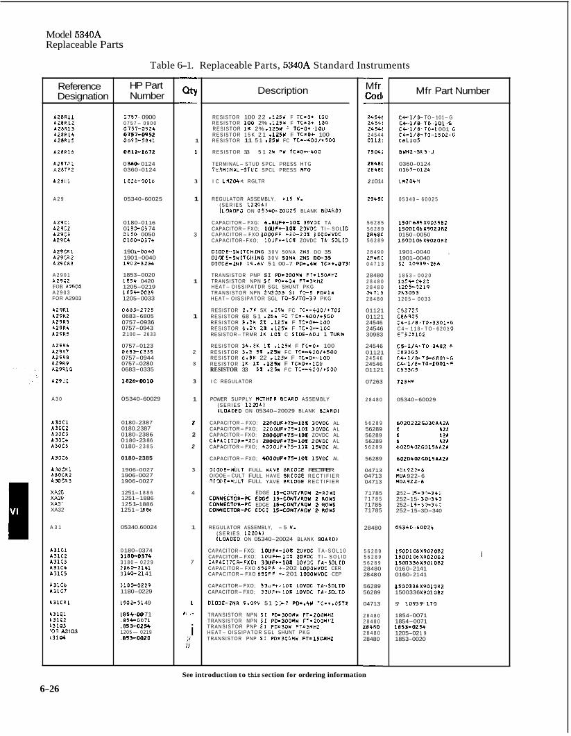
Model 5340A Replaceable Parts
Reference Designation
A 2 8 R 1 1 A 2 8 R 1 2 A 2 8 R 1 3 A 2 8 R 1 4 A 2 8 R 1 5
A 2 8 R 1 6
A 2 8 T P l A 2 8 T P 2
A Z 8 U 1
A 2 9
A 2 9 C 1 A 2 9 C 2 A 2 9 C 3 A 2 9 C 4
A 2 9 C R 1 A29CRZ A 2 9 C R 3
A 2 9 0 1 A 2 9 9 2 FOR A2902 A 2 9 0 3 FOR A2903
A 2 9 R 1 A 2 9 R Z A 2 9 R 3 A 2 9 R 4 A 2 9 R 5
A 2 9 R 6 A 2 9 R 7 A29118 129119 A 2 9 R 1 0
A 2 9 U l
A 3 0
A 3 0 C l A 3 0 C 2 4 3 0 C 3 A 3 0 C 4 A 3 0 C 5
A3OC6
A 3 0 C R 1 A 3 0 C R 2 A 3 0 C R 3
XAZ8 XA29 XA31 XA32
A 3 1
A 3 1 C l A 3 1 C 2 A 3 1 C 3 A 3 1 C 4 A 3 1 C 5
A 3 1 C 6 A 3 1 C 7
A 3 l C R l
L3101 L 3 1 0 2 43193
t31W -OR ~ 3 1 0 3
Table 6-1. Replaceable Parts, 5340A Standard Instruments
HP Part Number
0757.. 0900 0 7 5 7- 0 9 0 0 0757-0924 0757-0952 0698-5841
0811-1672
0 360- 0124 0360-0124
1826-0016
05340-60025
0180-01 16 0 180-03 74 0 1 5 0 - 0050 0180-0374
190 1-0040 190 1-0040 3902-3234
1853-0020 1 8 5 6 0420 1205-0219 1854-0039 1205-0033
0 6 8 3 - 2 7 2 5 0683-6805 0757-0936 0757-0943 2 1 0 0- 2 6 3 3
0757-0123 0683-0335 0757-0944 0757-0280 0683-0335
182&0010
0 5340- 60029
0180-2387 0180.2387 0180-2386 0 180- 23 86 0180- 2 3 8 5
0180-2385
1906-0027 1906-0027 1906-0027
1251- 1 8 8 6 1251-1886 125 1- 1886 1251-1 886
05340.60024
0 180-0374 0180-0374 3 1 8 0- 0 2 2 9 D 1 6 D - 2 1 4 1 3 160-21 41
0 1 8 0 - 0 2 2 9 1180-0229
1902-31 49
1854-00 71 1854-0071 1853-0254 1205- 0219 ,853-0020
- QtY -
1
1
3
1
3
1
1
2
3
3
1
2
2
2
3
4
1
7
1
I ! , (
i ;i
Description
RESISTOR 100 22 .125W F TC=O+ 100 R E S I S T O R 100 2% .125W F TC=O+ 100 R E S I S T O R 1 K 2% -125W F T C - 0 + ~ 1 0 0 R E S I S T O R 1 5 K 2 1 .125Y F TC=O+. 100 R E S I S T O R 11 5 1 .25Y FC T C * - 4 0 0 / + 5 0 0
R E S I S T O R 3.3 5 1 2U PW TC=0+-400
TERMINAL- STUD SPCL PRESS H T G TERMINAL-STUG SPCL PRESS HTG
I C LMZO4H RGLTR
REGULATOR ASSEMBLY, + 1 5 V. ( S E R I E S 1 2 2 O A l (LOAOFO O N 05340-201325 BLANK BDAROl
CAPACITOR- FXG: 6.8UF+-101 35VOC TA CAPACITOR- FXO; l O U F + - l O Z ZOVDC T I- S O L I0 CAPACITOR- FXO l O O O P F +80-202 lOOOUVOC CAPACITOR- FXO; lOUF+-102 ZOVDC T I - S O L I D
D I O D E - S Y I T C H I N G 3 0 V 5 0 N A ZNS DO 35 OIOOE-SWITCHING 3 0 V 5 0 N A 2NS O W 3 5 D I M E - Z N R 19.6V 5 1 00-7 P0=.4W TC=+.073'
TRANSISTOR PNP SI PD-3OOHY F T - 1 5 0 M H Z TRANSISTOR NPN SI P 0 - 4 0 Y FT-3MHL H E A T- O I S S I P A T D R SGL SHUNT PKG T R A N S I S T O R NPN 2 N 3 0 5 3 SI 10-5 P O = l Y H E A T- O I S S I P A T O R SGL TO-51TO-39 P K G
RESISTOR 2.7K 5X .25W FC T C - - 4 0 0 / + 7 0 0 R E S I S T O R 68 5 1 .25U FC T C s - 4 0 0 / + 5 0 0 R E S I S T O R 3.3K 22 -125W F T C = O t - l O O R E S I S T O R 6.21 2X .125W F T C - O c l O O RESISTOR- TRMR I K 101 C S I D E - A O J 1 TURN
R E S I S T O R 34 .8K 11 .125W F TC=O+ 100 R E S I S T O R 3-3 5% -2% F C T C - - 4 0 0 1 + 5 0 0 R E S I S T O R 6-8K 22 -12% F TC=O+-100 R E S I S T O R 1 K 1% .125Y F T C = 0 + - 1 0 0 RESISTOR 3.3 5X .2H1 F C T C ~ - 4 0 0 / + 5 0 0
I C REGULATOR
POWER SUPPLY MOTHFR BOAR0 ASSEMBLY ( S E R I E S 1 2 2 O A l (LOADED ON 05340-20029 BLANK BOAR01
CAPACITOR- FXO: 2 2 0 O U F + 7 5 - 1 0 % 30VOC AL CAPACITOR- FXO; 2200UF+75-102 3 0 V D C A L CAPACITOR- FXO: 280WF+75-101 ZOVDC AL CAPACITOR-FXD; 2 8 0 0 U F + 7 5 - 1 0 % 2OVOC A L CAPACITOR- FXO; 4 0 0 0 U F + 7 5 - 1 0 1 l 5 V O C AL
CAPACITOR- FXO; 400WF+75-101 15VDC AL
DIODE-H~LT FULL YAVE B R I D G E RECTIFIER OIOOE- CULT FULL HAVE BRIOGE R E C T I F I E R D1I)E-MULT FULL YAVE BRIOGE R E C T I F I E R
CONNECTOR-PC EDGE 15-CONTIROW 2-ROYS CONNECTOR-PC EDGE 15-CONTIROY 2 ,ROWS CONNECTOR-PC EDGE 15-CONT/SOW 2-ROYS CONNECTOR-PC EDGE 15-CONTIROW 2-ROWS
REGULATOR ASSEMBLY, - 5 V. ( S E R I E S l Z Z O A l I L O A O E D ON 05340-20024 BLANK BOAR01
CAPACITOR- FXG: l O U F + - 1 0 2 ZOVOC T A - S O L 1 0 CAPACITOR- FXO: l O U F C l O 2 ZOVDC T I - S O L I D C A P A C I T O R - F X O i 33UF+-101 lOVOC T A - S O L 1 0 CAPACITOR- FXO 6 8 0 P F +-202 lOOOYVOC CER CAPACITOR- FXO 6 8 0 P F +- 201 lOOOWVOC CEP
CAPACITOR- FXO; 3 3 U F + = 1 0 1 l O V D C TA-*SOL10 CAPACITOR- FXO; 3 W F C l 0 1 lOVOC TA-SOL10
D IODE-ZNR 9.09V 51 0*7 PO=.4W TC-+.0571
TRANSISTOR NPN S I PO-3OOMW FT-ZOOHHZ TRANSISTOR NPN SI PD-300MW FT-200MHZ T R A N S I S T O R PNP SI P0=30W FT-3MHZ H E A T- O I S S I P A T O R SGL SHUNT P K G TRANSISTOR PNP S I W - 3 0 G M U FT=lSOHHZ
- Mfr Cod1 - 2 4 5 4 f 2 4 5 4 f 2 4 5 4 f 2 4 5 4 4 0 1 1 2 1
75041
2849C 2848C
21 01 4
2848C
5 6 2 8 5 5 6 2 8 9
5 6 2 8 9
2 8 4 9 0 2R4RO 0 4 7 1 3
28480 2 8 4 8 0 2 8 4 8 0 0 4 7 1 3 2 8 4 8 0
01121 01121 24546 24546 30983
24546 01 121 2 4 5 4 6 24546 01121
07263
2848a
2 8 4 8 0
5 6 2 8 9 56289 56289 56289 5 6 2 8 9
56289
04713 04713 04713
71785 7 1 7 8 5 71785 71785
28480
5 6 2 8 9 5 6 2 8 9 5 6 2 8 9 28480 28 48 0
56289 56289
04713
2 8 4 8 0 2 8 4 8 0 284RO 2 8 4 8 0 28480
-
Mfr Part Number
C 4 - 1 1 8 - TO- 101- G C 4 - 1 / 8 ~ T D - l O l ~ G C4-118- 10-1 001 - G C 4 - 1 1 8 - T O - 1 5 0 2 - G C 8 1 1 0 5
0360-0124 0 3 6 0 - 0 1 2 4
L H 2 0 4 H
0 5 3 4 0 - 6 0 0 2 5
150D685 X 9 0 3 5 E Z 1 5 O D 1 0 6 X 9 0 2 0 R Z 0150-0050 1 5 0 D 1 0 6 X 9 0 2 0 8 2
1901-0040 , 1901-0040 SZ 10939-266
1 8 5 3 - 0 0 2 0 1 8 5 4 - 0 4 2 0 1 2 0 5 - 9 2 1 9 2 N 3 0 5 3 1 2 0 5- 0 0 3 3
C 8 2 7 2 5 C 8 6 8 0 5 C 4 - 1 1 8 - T O - 3 3 0 1 - G C 4 - 1 1 8 - T O - 6 2 0 1 -G E T 5 O X 1 0 2
C 5 - 1 / 4 - T O - 3 4 8 2 , F C 8 3 3 G 5 C 4 - 1 1 8 - T L l - 6 8 0 1 - G C 4 - 1 1 8 - T 0 * 1 0 0 l - F C 8 3 3 G 5
7 2 3 H M
05340-60029
6 0 2 D 2 2 2 G 0 3 0 A A Z A 6 0 2 0 2 8 2 G 0 2 0 A A Z A 6 0 2 0 2 8 2 G O Z O A A Z A 6 0 2 0 4 O Z G 0 1 5 A A 2 A
H O A 9 2 2 - 6 MDA 92 2- 6 WDA922-6
2 52- 1 5-3'?-340 252-15- 30-3'+0 252- 15-30-340 252-1 5-3D-340
0 5 3 4 0 - 6 0 0 2 4
I 1 5 0 D 1 0 6 X 9 0 2 0 8 2 1 5 0 0 1 0 6 X 9 0 2 0 8 2 1 5 0 0 3 3 6 X 9 0 1 0 8 2 016 0- 21 41 0160- 21 41
1 5 0 D 3 3 6 X 9 0 1 0 8 2 1500336 X 9 0 1 0 8 2
S.? 1 0 9 3 9 - 1 7 0
1854- 0071 1854-0071 1853-02% 1205-02 1 9 1853-0020
See introduction to this section for ordering information
6-26
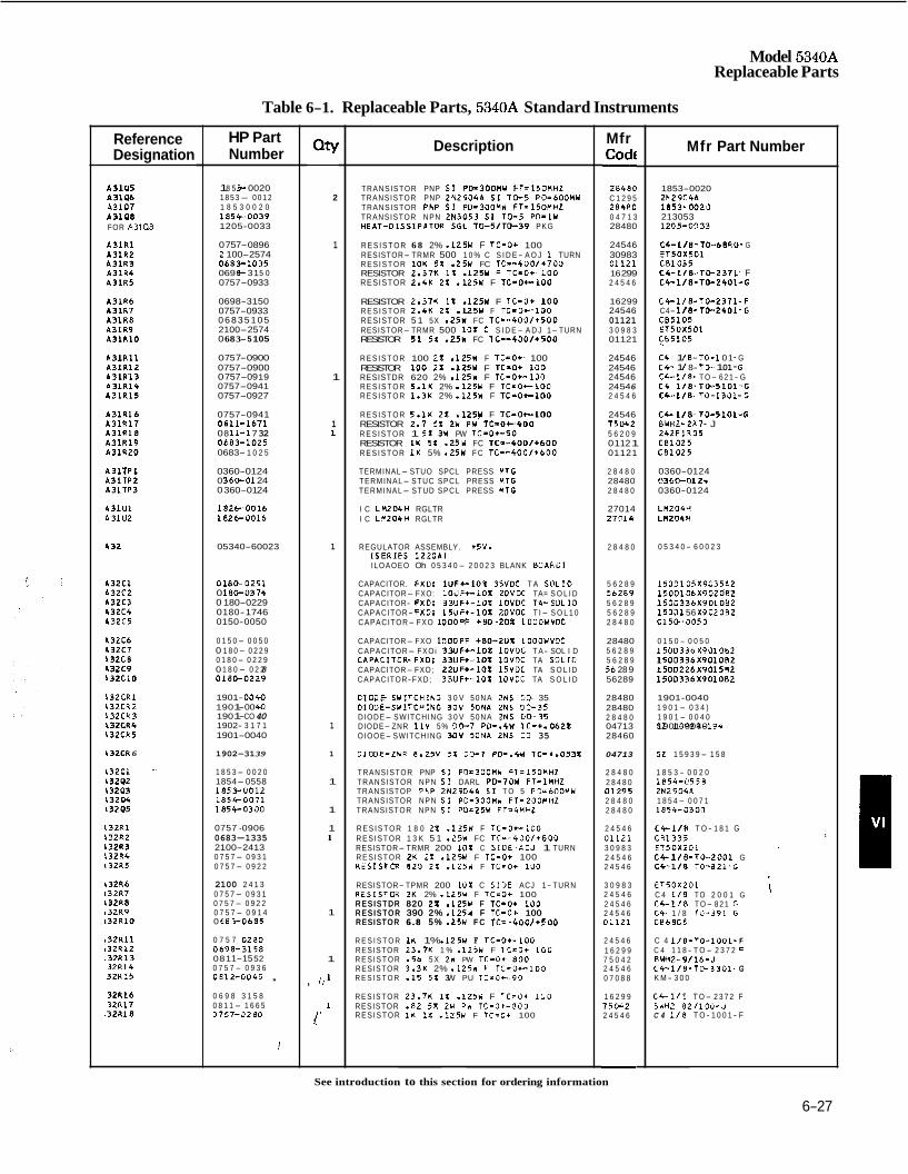
Model 5340A Replaceable Parts
Table 6-1. Replaceable Parts, 5340A Standard Instruments
Reference Designation
~ 3 1 ~ 5 ~ 3 1 ~ 6
~ 3 1 ~ 8 4 3 1 0 7
FOR A31QB
A 3 1 R 1 A 3 1 R Z A 3 1 R 3 A 3 1 R 4 A 3 1 R 5
A 3 1 R b A 3 1 R 7 A31RB A 3 1 R 9 A 3 1 R 1 0
A 3 1 R l l A 3 1 R 1 2 A 3 1 R 1 3 A 3 1 R 1 4 A 3 1 R 1 5
A 3 1 R 1 6 A 3 1 R 1 7 A 3 1 R 1 8 A 3 1 R 1 9 A31RZO
A 3 1 T P 1 A 3 1 T P Z A 3 1 T P 3
A 3 1 U 1 A 3 1 U 2
b 32
L 3 2 C 1 A 3 2 C 2 A32C3 L 3 Z C 4 L 3 2 C 5
L 3 2 C b A 3 2 C 7 4 3 2 C 8
k 3 2 C 1 0
4 3 2 C R 1 432CRZ 4 3 2 C R 3 4 3 2 0 7 4 432CR5
i 3 2 C R 6
n32c9
w a i - w a 2 m a 3
i3za5 i 3294
1 3 2 R 1 i 3 2 R Z 132R3 1 3 2 R 4 l 3 2 R 5
l32R6
13263 i 3 2 R 7
t 3 2 R 9 i 3 2 R 1 0
832R11 132R12 ,321113 3 2 R 1 4 3 2 R 1 5
321116 3 2 R 1 7
. 3 2 R l 8
HP Part Number
1 8 5 3- 0020 1 8 5 3- 0 0 1 2 1 8 5 3 0 0 2 0 1 8 5 4 . 0 0 3 9 1205-0033
0 757- 0896 2 100-2574 0683-1035 069 8- 31 5 0 0757-0933
0698-3150 0757-0933 06835105 2100-2574 0 68 3- 5 105
0 75 7- 0900 0757-0900 0 757-09 19 0757-0941 0757-0927
0757-0941 0811-1671 0 8 11-1 7 32 0683-1025 0683- 1 0 2 5
0360-0124 0 360-01 24 0 360-01 24
1 8 2 6 . 0 0 1 6 18260016
05340-60023
0180-0291 0 100-0374 0 180-0229 0 180- 1746 0150-0050
0 1 5 0 - 0 0 5 0 0 1 8 0- 0 2 2 9 0 1 8 0 - 0 2 2 9 0 1 8 0- 0 2 2 8 0 1 8 0 - 0 2 2 9
1901- 0040 190 1- 00 40 190 1- CO 40 1902- 3 1 7 1 1901-0040
1902-31 39
1 8 5 3 - 0 0 2 0 1854-0558 1 8 5 3 - O C 1 2 1 8 5 4 - 0 0 7 1 1854-0330
0757 -0906 0683-1335 2100-2413 0 7 5 7- 0 9 3 1 0 7 5 7- 0 9 2 2
2100 2 4 1 3 0 7 5 7- 0 9 3 1 0 7 5 7- 0 9 2 2 0 7 5 7 - 0 9 1 4 0 682-0685
0 7 5 7 0280 0 6 9 8 - 3 1 5 8 081 1-15 52 0 7 5 7 - 0 9 3 6 0 8 1 2 - 0 0 4 5 ,
0 6 9 8 3 1 5 8 0 8 1 1- 1 6 6 5 0 7 5 7 - i I 2 8 0
I
QW - 2
1
1
1 1
1
1
1
1
1
1 1
1
1
, il'
I!
Description
TRANSISTOR PNP SI PO-3OOMU F T = 1 5 0 M H L TRANSISTOR PNP 2 N 2 9 0 4 A S I 10-5 PD-6OOMU TRANSISTOR P h P SI PD-3OOMW FT-15OMHZ TRANSISTOR NPN 2 N 3 0 5 3 51 10-5 PD- lW H E A T - D I S S I P L T O R SGL TO-5/TO-39 PKG
R E S I S T O R 6 8 2% - 1 2 5 W F TC=O+ 100 RESISTOR- TRMR 500 1 0 % C S I D E- A O J 1 TURN R E S I S T O R 1 0 K 5 1 -25Y FC T C = - 4 0 0 / + 7 0 0
RESISTOR 2.4K 2 X . 1 2 5 Y F T C = O t - l O O RESISTOR 2.37~ 1 % .i25w F T C - o c i o o
RESISTOR 2 . 3 7 ~ 1% .i25n F T C = O + l o o R E S I S T O R 2.4K ZX -125W F T C - O c - 1 0 0 RESISTOR 5 1 5X .25W FC T C = - 4 0 0 / + 5 0 0 RESISTOR- TRMR 500 10% C S I D E- A D J 1- TURN RESISTOR 5 1 5% .25w FC T C - - ~ O O / + ~ O O
R E S I S T O R 100 Z X .125W F TC=O+- 100 RESISTOR loo z x .MW F T c = o + 100 RESISTDR 620 2% .125Y F TC-0-100 R E S I S T O R 5.1K 2% .125W F T C - O r 1 0 0 R E S I S T O R 1.3K 2% . 1 2 5 Y F T C = O c 1 0 0
R E S I S T O R 5.1K Z X .125)r F TC-O+-100
R E S I S T O R 1 5 1 3W PW TC-O+-50
R E S I S T O R 1 K 5% .25W F C T C - - 4 0 0 / + 6 0 0
TERMINAL- STUO SPCL PRESS MTG TERMINAL- STUC SPCL PRESS MTG TERMINAL- STUD SPCL PRESS M T 6
I C L M 2 0 4 H RGLTR I C LMZO4H RGLTR
RESISTOR 2.7 5 s zw pw T C = O + ~ O O
RESISTOR IK 5 % .z5w FC T C = - ~ O O / + ~ O O
REGULATOR ASSEMBLY. +5V. ( S E R I E S 1 2 2 0 1 ) ILOAOEO Oh 0 5 3 4 0- 2 0 0 2 3 BLANK BOARD1
CAPACITOR. FXO; l U F C - l O % 35VOC T A S O L 1 0 CAPACITOR- FXO: l O U F c l O 2 ZOVOC TA= S O L I D CAPACITOR- FXO; 3 3 U F + - l O % l O V D C T A - S O L 1 0 CAPACITOR- FXO: I 5 U F + - 1 0 % ZOVDC T I - S O L 1 0 CAPACITOR- FXO IOOOPF + 8 0 - 2 0 X lOOOYVOC
CAPACITOR- FXO lOOOPF +80-20% lOOOWVDC CAPACITOR- FXOi 3 W F + - l O % IOVOC T A- SOL I D CAPACITOR-FXD; 3 3 U F + - l O % l 0 V K TA S O L 1 0 CAPACITOR- FXO; Z Z U F + - l f l % l 5 V D C TA S O L I D CAPACITOR- FXD; 3 3 U F + - l O % lOVOC TA S O L I D
C IDOi+SYITCHING 3 0 V 5 0 N A ZNS OD 35
DIODE- SWITCHING 3 0 V 5 0 N A 2NS U P 3 5 DIODE- ZNR 1 1 V 5% DG-7 PD-.4W TC=+.062X OIOOE- SWITCHING M Y 5 0 N A ZNS 00 35
D I M E - L N R 8.25V 5 X 00-7 PD=.4W T C = + . 0 5 3 4
DIOOE-SWITCHING 3ov ~ O N A ZNS 00-35
TRANSISTOR PNP 5 1 PD=300MU FT= lSOMHZ TRANSISTOR NPN SI DARL PD=70Y F T = l M H Z TRANSISTOP P L P 2 N 2 9 0 4 A S I T O 5 PD=600MW TRANSISTOR NPN SI P0=300MW FT=200MHZ TRANSISTOR NPN 5 1 P0-25W FT-4MCL
R E S I S T O R 1 8 0 2% .125W F T C = O t - 1 0 0 R E S I S T O R 1 3 K 5 1 .25W FC T C = - 4 0 0 / + 8 0 0 RESISTOR- TRMR 200 1 0 % C S I O E - A D J 1 TURN R E S I S T O R ZK 22 .12W F TC-O+ 100 RESISTCS! BZO Z X .125W F TC=O+ 100
RESISTOR- TPMR 200 102 C S I D E ACJ 1- TURN R E S I S T O H ZK 2% .125W F TC=O+ 100 R E S I S T D R 820 Z X .125W F TC=O+ 100 R E S I S T O R 390 2% .125Y F TC=O+ 100 RESISTOR 6 . 8 5 % .25W F C T C = - 4 0 0 / + 5 0 0
R E S I S T D R 820 Z X .125W F TC=O+ 100 R E S I S T O R 390 2% .125Y F TC=O+ 100 RESISTOR 6 . 8 5 % .25W F C T C = - 4 0 0 / + 5 0 0
R E S I S T O R 1 K 1% .125W F T C - O + - 1 0 0 RESISTOR 23.7K 1 % .125W F TC-O+ l G 0 R E S I S T O R - 5 6 5 X 2W PW TC-O+ 8 0 0 RESISTOR 3.3K 2% .125W F TC-O+-100 R E S I S T O R - 1 5 5 1 3W PU TC=0+-90
R E S I S T O R 23 .7K I X .125* F TC=O+ l G 0 RESISTOR - 8 2 5% 2W PW T C = 0 + - 8 0 0 R E S I S T O R 1 K 1Z .125W F T C - 0 t 100
Mfr Codf - 28480 C 1 2 9 5 2 8 4 8 0 0 4 7 1 3 28480
24546 30983 01121 16 299 2 4 5 4 6
16299 24546 01121 3 0 9 8 3 01121
24546 24546 24546 24 54 6 2 4 5 4 6
24546 7 5 0 4 2 5 6 2 0 9 01 12 1 01121
2 8 4 8 0 28480 2 8 4 8 0
27014 27014
2 8 4 8 0
5 6 2 8 9 56269 5 6 2 8 9 5 6 2 8 9 2 8 4 8 0
28480 5 6 2 8 9 5 6 2 8 9 56 28 9 56289
28480 28480 2 8 4 8 0 04713 28460
04713
2 8 4 8 0 2 8 4 8 0 0 1 2 0 5 2 8 4 8 0 2 8 4 8 0
2 4 5 4 6 0 1 1 2 1 3 0 9 8 3 2 4 5 4 6 2 4 5 4 6
3 0 9 8 3 2 4 5 4 6 2 4 5 4 6 2 4 5 4 6 0 1 1 2 1
2 4 5 4 6 1 6 2 9 9 7 5 0 4 2 2 4 5 4 6 0 7 0 8 8
1 6 2 9 9 7 5 0 4 2 2 4 5 4 6
-
Mfr Part Number
1853-0020 Z M 2 9 0 4 A 1 8 5 3 - 0 0 2 3 213053 1205-0033
C4-1/8-TO-b8RO. G E T 5 0 X 5 0 1 C B 1 0 3 5 C 4 - l / & r O - 2 3 7 1 - F C 4 - 1 / 8 - 1 0 - 2 4 0 1 - G
C 4 - 1 / 8 - T O - 2 3 7 1 - F C4- 1 / 8 - T O - 2 4 0 1 - G C 6 5 1 0 5 E T 5 0 X 5 0 1 $85105
C 4 - 1 /8- 10-1 01 - G CC- 1 / 8- T 0- 1 01 - G C 4 - 1 / 8 - T O- 6 2 1- G C 4 1 / 8 - T O - 5 1 0 1 - G C 4 = 1 / 8 - T O - 1 3 0 1 - G
C 4 - 1 / 8 - T O - 5 1 0 1 - G 8WHZ-ZR7- J 2 4 2 E l R 0 5 C 8 1 0 2 5 C 8 1 0 2 5
0360-0124 0360-012+ 0360-0124
L M 2 0 4 H L M Z 0 4 H
0 5 3 4 0 - 6 0 0 2 3
1 5 0 D 1 0 5 X 9 0 3 5 A 2 1 5 0 0 1 0 6 X 9 0 2 0 8 2 1 5 0 D 3 3 6 X 9 0 1 0 B 2 15001 56 X902082 0150-005J
0 1 5 0 - 0 0 5 0 1500336 X 9 O l 0 8 2
1901-0040 1 9 0 1 - 0 3 4 ) 1 9 0 1 - 0 0 4 0 SZ 1901-0040 1 O S 3 9 - 1 9 4
S Z 1 5 9 3 9 - 1 5 8
1 8 5 3 - 0 0 2 0 1 8 5 4 - 0 5 5 8 2 N 2 9 0 4 A 1 8 5 4 - 0 0 7 1 1 8 5 4 - 0 3 0 0
C 4 - l l 8 T O - 1 8 1 G C B 1 3 3 5 E l 5 O X 2 0 1 C C l / 8 - T 3 - ~ 2 0 0 1 G C 4 - l l R T O - 8 2 1 - G
E T 5 0 X Z 0 1 C 4 1 1 8 TO 2 0 0 1 G C 4 - 1 / 8 T O- 8 2 1 G C C 1 / 8 TJ-391 G C B 6 8 G 5
C 4 1 / 8 - ~ O - l O O l - F C 4 1 1 8 - T O- 2 3 7 2 F RWHZ- 9 /16 -J C 4 - 1 / 8 = 1 0 - 3 3 0 1 - G K M - 3 0 0
C C l l 9 T O- 2 3 7 2 F 8WHZ 8 Z l l O G - J C 4 1 / 8 T O - 1 0 0 1 - F
See introduction to this section for ordering information
6-27
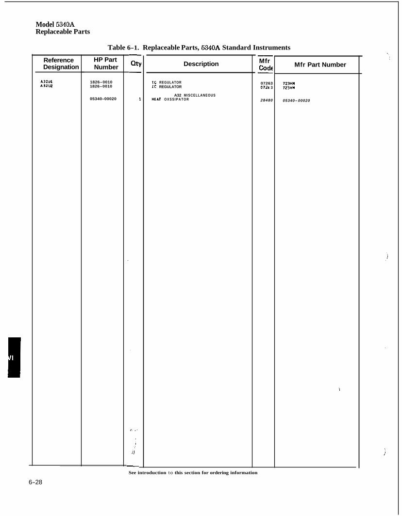
Model 534019 Replaceable Parts
Table 6-1. Replaceable Parts, 5340A Standard Instruments
Reference Designation
A32U1 A32112
HP Part Number
1826-0010 1826-0010
05340-00020
Description
XC REGULATOR IC REGULATOR
A32 MISCELLANEOUS HEAT O X S S I P A T O R
- Mfr Cod€ - 07263 0726 3
28480
Mfr Part Number
723HM 723HW
05340-00020
See introduction to this section for ordering information
6-28
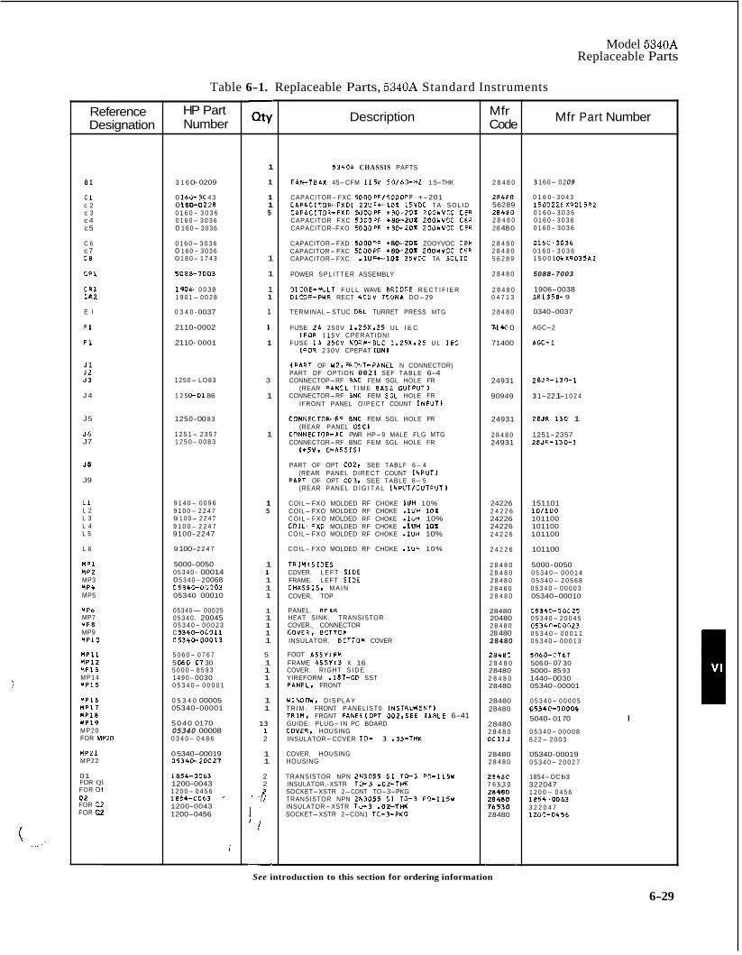
Model 5340A Replaceable Parts
i
c
Reference Designation
c1 c 2 c 3 c 4 c 5
C 6 c7 C 8
C P I
C R 1 CR2
E l
F 1
F 1
J1 J 2 5 3
J 4
J5
5 6 J7
J8
J9
L 1 L 2 L 3 L 4 L 5
L 6
MP1 MPZ MP3 MPC MP5
UP6 MP7 MP8 MP9 M P l O
U P 1 1 M P 1 2 MP13 MP14 M P l 5
Y P 1 6 MP17 M P l 8 MP19 MP20 FOR MP20
M P 2 1 MP22
01 FOR Ql FOR Q1 0 2 FOR Q2 FOR a2
Table 6-1. Replaceable Parts, 5340A Standard Instruments
HP Part Number
3 1 6 0- 0209
0 16U- 3C 4 3 0 180-02 2 6 0 1 6 0 - 3 0 3 6 0 1 6 0- 3 0 3 6 0 1 6 0- 3 0 3 6
0 1 6 0- 3 0 3 6 0 1 6 0- 3 0 3 6 0 1 8 0- 1 7 4 3
5088-7003
1906, 0 0 3 8 1 9 0 1- 0 0 2 8
0 3 4 0 - 0037
2110-0002
2110- 0001
1250- LO83
1 2 5 0-01 86
1250- 00 8 3
1 2 5 1- 2 3 5 7 1 2 5 0- 0 0 8 3
9 1 4 0- 0 0 9 6 9 1 0 0- 2 2 4 7 9 1 0 0- 2 2 4 7 9 1 0 0 - 2 2 4 7 9100-2247
9 100- 2 2 4 7
5000-0050 0 5 3 4 0- 00014 0 5 3 4 0- 2 0068 C 5 3 4 0 - 0 0 0 0 3 05340 00010
05340- 00025 0 5 3 4 0 . 20045 0 5 3 4 0- 0 0 0 2 3 C 5340-0C'311 0 5 3 4 ~ - 0 0 0 1 3
5 0 6 0- 0 7 6 7 5 C-5 0-07 30 5 0 0 0- 8 5 9 3 1 4 9 0- 0030 0 5 3 4 0 - 0 0 0 0 1
0 5 3 4 0 00005 05340-00001
5040 0170 05340 00008 0 3 4 0 - 0 4 8 6
0 5340-00019 0534C-20027
1854-0063 1200-0043 1 2 0 0- 0 4 5 6 1 8 5 4 - 0 0 6 3 1200-0043 1200-0456
/
1
1
1 1 5
1
1
1 1
1
1
1
3
1
1
1 5
1 1 1 1 1
1 1 1 1 1
5 1 1 1 1
1 1
13 1 2
1 1
2 2
' 8 I ; -
Description
5 3 4 0 A CHASSIS PAFTS
FAN-T0AX 45-CFM 1 1 5 V 5 0 1 6 0 - H L 1.5-THK
CAPACITOR- FXC 5OOOPF15OOOPF +-201 CAPACIT3R-FXO; 2 2 U F C - 1 0 1 i 5 V O C T A - S O L I D CAPACITOQ-FXC 5OOOPF + 8 0 - 2 O Z ZOOYVDC CER CAPACITOR FXC 5DUOPF +8012U? ZOOYVDC CFR CAPACITOR-FXO 5 0 0 0 P F +80-20X 2OOWVDC CER
CAPACITOR-FXD 5 0 0 0 P F + 8 0 ~ 2 O Z ZOOYVOC CER CAPACITOR-FXC 5 0 0 0 P F +80-201 2OOWVDC CFR CAPACITOR-FXC: . l U F C - l O X 35VOC TA SOLID
POWER S P L I T T E R ASSEMBLY
D I O D E - W L T F U L L WAVE BRIDGE R E C T I F I E R 0 IM)E-PYR RECT 4 0 0 V 7 5 0 N I DO- 29
TERMINAL- STUC DRL TURRET PRESS MTG
FUSE 2 A 2 5 0 V 1.25X.25 UL I E C IFOR 1 1 5 V CPERATIDNI
FUSE 1 A 25DV NORM-8LO 1.25X.25 U L I E C I F O R 2 3 0 V CPEPAT ION1
(PART OF Y2.FRDNT-PANtL N CONNECTOR) PART DF OPTION 0021 SEF TABLE 6-4 CONNECTOP-RF 8NC FEM SGL HOLE FR
(REAR DANEL T I M E BASE OUTPUT1 CONNECTOR-RF 0NC FEM SGL HOLE FR
IFRONT PANEL OIPECT COUNT I N P U T 1
CONNFCTOR-RF 0NC FEM SGL HOLE FR
CONNECTOP-AC PWR HP-9 MALE FLG MTG CONNECTOR-RF BNC FEM SGL HOLE FR
(REAR PANEL D S C l
(+5V. CHLSSISI
PART OF OPT 002. SEE TABLF 6 - 4 (REAR PANEL DIRECT COUNT I N P U T 1
P A P 1 OF OPT 003. SEE TABLE 6- 5 (REAR PANEL D I G I T A L INPUTIOUTPUT)
COIL- FXO MOLDED RF CHOKE 1UH 10% COIL- FXO MOLDED RF CHOKE . l U H 10% COIL- FXO MOLDED RF CHOKE -1UH 10% C C I L - F X D MOLDED RF CHOKE -1UH 1OZ COIL- FXO MOLDED RF CHOKE .1UH 10%
COIL- FXO MOLDED RF CHOKE -1UH 10%
1RIM:SIDES COVER. L E F T SIDE FRAME. LEFT S I D E CHASSISv M A I N COVER, TOP
PANEL. RELR HEAT SINK. TRANSISTOR COVER. CONNECTOR COVER, BOTTOC INSULATOR. 8DTTOM COVER
FOOT ASSY:FM FRAME ASSY:3 X 16 COVER. RIGHT S I D E YIREFORM .187-00 SST PANEL, FRONT
UINOOUI D I S P L A Y T R I M . FRONT PANELIST0 INSTRUMENTI TRIM, FRGNT PANELIDPT 002.SEE TABLE 6-41 GUIDE: PLUG- IN PC BOARD COVERI HOUSING INSULATOR-CCVER TO- 3 .33-THK
COVER, HOUSING HOUSING
TRANSISTOR NPN 2 N 3 0 5 5 SI 10-3 P0=115Y INSULATOR,-XSTR T W 3 .OZ-TK SOCKET-XSTR 2-CONT TO-3-PKG TRANSISTOR NPN 2 N 3 0 5 5 SI 10-3 P 0 = 1 1 5 U INSULATOR-XSTR 10-3 .02-THK SOCKET-XSTR 2-CON1 TO-3-PKG
Mf r Code
2 8 4 8 0
2fl4PO 56289 2 8 4 8 0 2 8 4 8 0 28 48 0
2 8 4 8 0 2 8 4 8 0 5 6 2 8 9
2 8 4 8 0
2 8 4 8 0 0 4 7 1 3
2 8 4 8 0
7-1 *o 0
71400
24931
90949
24931
2 8 4 8 0 24931
24226 2 4 2 2 6 24226 24226 2 4 2 2 6
2 4 2 2 6
2 8 4 8 0 2 8 4 8 0 2 8 4 8 0 2 8 4 8 0 2 8 4 8 0
28480 20480 2 8 4 8 0 28 480 28480
28480 2 8 4 8 0 28480 2 8 4 8 0 28480
28480 28480
28480 2 8 4 8 0 O O l l J
28480 2 8 4 8 0
2 8 4 8 0 7 6 5 3 0
28480
Mfr Part Number
3 1 6 0- 0 2 09
0 1 6 0 - 3 0 4 3 1 5 0 0 2 2 6 X 9 0 1 5 R 2 0 1 6 0 - 3 0 3 6 0 1 6 0 - 3 0 3 6 0 1 6 0- 3 0 3 6
0 1 6 0 - 3 0 3 6 0 1 6 0 - 3 0 3 6 1 5 0 0 1 0 4 X 9 0 3 5 A 2
5088-7003
1906-0038 SR1358- 9
0340-0037
AGC-2
AGC-1
28JR-130-1
3 1-22 1- 1 0 2 4
2 B J R - 1 3 0 1
1251-23 57 ZBJR- 130-1
151101 101l00 101100 101100 101100
101100
5000-0050 0 5 3 4 0- 0 0 0 1 4 0 5 3 4 0- 2 0 5 6 8 0 5 3 4 0- 0 0 0 0 3 05340-0001 0
0534C-OJCZ5 0 5 3 4 0- 2 0 0 4 5 C534C-CO923 0 5 3 4 0 - 0 0 0 1 1 0 5 3 4 0- 0 0 0 1 3
5 0 6 3 - 0 7 6 7 506 0- 07 30 5000- 85 93 144 0- 00 30 05340-00001
0 5 3 4 0- 0 0 0 0 5 G5340- i70004 5040- 01 70 I
0 5 3 4 0- 0 0 0 0 8 6 2 2- 2 0 0 3
05340-00019 0 5 3 4 0- 2 0 0 2 7
1854-OC b3 322047 1 2 0 0- 0 4 5 6 1854-0063 3 2 2 0 4 7 1200-0156
See introduction to this section for ordering information
6-29
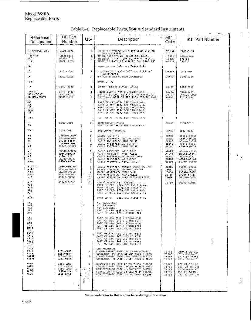
Model 5340A Replaceable Parts
Table 6-1. Replaceable Parts, 53404 Standard Instruments
I
Reference Designation
R 1 SAMPLE RATE
FOR R 1 R 2 R 3
R 4
s1
5 2
s3
5 4
FOR 54 S5 (INT-EXT) S6 (1 15V-230V)
57 S 8 5 9 s 10 S l l
5 1 2
T I 1 2
TH1
Y 1 UP W3 Y 4 us
Y b Y 7 Y 8 Y 9 u 10
u11 . Y 1 2 Y 13 Y 1 4 Y 1 5
Y 1 6 W l 7 Y 18 Y I P uzo
Y t l
XA1 XA2 XA3 XA4 XA5
XA6 XA7 X I 8 X A 9 X A l O
X A l l X A 1 2 X A 1 3 X I 1 4 X A 1 5
X A 1 6 X A 1 7 K A l 8 KA19A X A I W
KA20 ( A 2 1 CA22 ( A 2 3 CA2+
HP Part Number
2100- 3171
0370-1099 0683-1025 0 6 8 3- 2 7 2 5
3 101- 16 94
3101- 1216
3 1 0 0- 2 9 3 5
0 3 7 0- 0 4 3 2 3101-0070 3 10 1-12 72
9 100- 3019
3103-0022
05505-60019 05340-60028 C 5 3 4 C - 6 0 0 3 3 0 5 3 4 W 6 0 0 3 4 0 5 3 4 0- 6 0 0 1 3
05340-60035 0 5 3 4 0 - 6 0 0 4 4 8120-1378 05340-60048 0 5 3 4 0 . 6 0 0 4 9
05340-60050 0 5 3 4 0- 6 0 0 5 1 05340 6 0 0 5 2 0 5 3 4 0- 6 0 0 5 3 05340-60054
05340= 6 0 0 6 5
1 2 5 1 - C l W 1251;0159 1 2 5 1-01 59 1251-01 5 9
1251-0233 1 2 5 1- 0 2 3 3 1251-0233 ~
1251-0233 1251-0233
. I
/
QW - 1
1 1 1
1
1
1
1 1 1
I
1
1 1 1 1 1
I 1
1 I
1 1 1 1 1
1
1
3
5
" /I
! I
Description
RESISTOR-VAR W I S W 1M 30% lOCW SPST--NC
KNOB-RASE PTR - 5 I N JGK SGI-DECAL I S A Y P L E RATE1
RESISTOR 1K 5X -25W FC TC--4C*./+%C RFSISTOR 2.7K 5 Z .25W FC TC- 400/+700
PART OF OPT 002. SEE T 4 B L E 6 .4 .
SWITCH-TGL SUBMIN IJPOT NS ZA 2 5 0 V A C
SWITCH-PB SPST NO MOM 25A (RESET)
PART OF R 1
I A C O N I O F F I
SWITCH.ROTARY, LEVER (RANGE)
KN0B:LEVERvOLIVE 8LACKlOPT X 9 5 SWITCH-SL OPOT-NS MINTR .5A 1 2 5 V A C I O C SWITCH-SL 4POT-NS STO 1.5A 250VAC SLOR
PART OF OPT 003. SEE TABLE 6 - 5 . PART OF OPT 003, SEE T A 8 L E 6-5. PPlRT OF OPT 003. SEE TABLF 6-5. PART OF OPT 003, SEE TABLE b-5. PART OF OPT 003, SEE TABLE 6-5 .
PART O F OPT 003. SEE TABLE 6-5.
TRANSFORMER: POUER PART OF OPT 001, SEE TABLE 6-3
SW1TCH:FXO THERMAL
CABLE. AC L I N E CABLE ASSEMBLVv 18 GHZ INPUT CABLE ASSEMBLYr SAMPLER I 1 CABLE ASSEPBLYI A3 OUTPUT CABLE ASSEMBLYw SAMPLER C2
CABLE ASSEMBLY, A 1 OUTPUT CABLE ASSEMBLY, VCO 1 / A l A Z CABLE A S S E M ~ L V Y I AC POUER CORD CABLE ASSECBLVv A2 OUTPUT CABLE ASSEMRLYI A 2 F L l INPUT
CABLE ASSEMBLYI DIRECT COUNT OUTPUT CABLE ASSEMBLY, 10 MHZ OOUBLFP CABLE ASSFMBLV, VCO l I A 2 2 CA8LE ASSEMBLY. VCO 21AZA2 CABLE ASSEMBLVe HARM FREP. A 1 4 I A 2 0
CA8LE ASSEMBLY t CHASSIS PART OF OPT. 302. SEE TABLE 6-4. PART OF OPT- 002. SEE TABLE 6- 4. PART OF OPT- 003 . SEE TABLE 6-5. PART OF OPT. 003. SEE TABLE b-5.
PART OF OPT. 003. SEE TA6LE 6 . 5 .
NOT ASSIGNED ._._ _ _ NOT ASSIGNEI, NOT ASSIGNEC PART OF A 1 6 (SEE L I S T I N G FORI PART OF A 1 6 ISEE L I S T I N G FOP1
PART O F A16 (SEE L I S T I N G FOR) PART O F A 1 6 (SFE L I S T I N G F O R I PART OF A 1 6 (SEE L I S T I N G FOR) PART OF A 1 6 (SEE L I S T I N G FOR1 PART OF A 1 6 (SEE L I S T I N G FOP1
PART OF A 1 6 (SEE L I S T I N G F 3 R I PART O F A 1 6 ISFE L I S T I N G FORI PART OF A 1 6 (SEE L I S T I N G FORI PART OF A 1 6 (SEE L I S T I N G FOR1 PART OF A 1 6 (SEE L I S T I N G FORI
NOT ASSIGNEC CONNECTOR-PC EDGE 15-CONTIROW 1-ROY CONNECTOR-PC EDGE 15-CONT/ROW 2-ROWS CONNECTOR-PC EDGE 15-CONTIROW 2-ROWS CONNECTOR-PC EnGE 15-CONTIROY 2.ROW.S
CONNECTOR-PC EDGE 22-CONTIROU 2-ROCIS CONNECTOR-PC EDGE 22-CONTIROY 2 R O Y S CONNECTOR-PC EDGE 22-CONTIROW 2-ROWS CONNECTOR-PC EDGE 22-CONTIROY 2-ROWS CONNECTOR-PC EDGE 22-CONTIROW >-ROWS
- Mfr Code
2 8 4 8 0
2 8 4 8 0 11121 01121
09 353
2 8 4 8 0
2 8 4 8 0
2 8 4 8 0 19727 28480
2 8 4 8 0
2 8 4 8 0
2 8 4 8 0 2 8 4 8 0 2 8 4 8 0 284RO 28 480
3 3 4 8 0 284RO 2 8 4 8 0 28480 28480
28480 2 8 4 8 C 28480 2 8 4 8 0 2 8 4 ~ 0
2 8 4 8 0
7 1 7 8 5 7 1 7 8 5
7 1 7 8 5
7 1 7 8 5 7 1 7 8 5 7 1 7 8 5 7 1 7 8 5 7 1 7 8 5
71785
-
Mfr Part Number
2100-31 71
0370- 1099 C P l " 2 5 C B 2 7 2 5
U3 1 8- PH 1
3 1 0 1 - 1 2 1 6
3 100- 2 9 3 5
0370- 0 4 3 2 GF-126- 0000 3 1 0 1 - 1 2 7 2
9100-3019
3103-0022
0 5 5 0 5 - 6 0 0 1 9 6 5 3 4 i - 6 C ' ) Z B 0 5 3 4 0- 6 0 0 3 3 0 5 3 4 0- 6 0 0 3 4 C5340-bO013
0 5 3 4 0- 6 0 0 3 5 05340-6OU4L
C 5 3 4 0 - 6 0 ? 4 8 0 5 3 4 0 - 6 0 0 4 9
0 5 3 4 0- 6 0 0 5 0 0 5 3 4 0- 6 0 0 5 1 0 5 3 4 0 - 6 0 0 5 2 C 5 3 4 0 - 6 0 0 5 3 05 3 4 0- 6 0054
05340-60065
e i z o - 1 3 7 8
250-15- 30-210 251-15- 3 0- 2 6 1 2 5 1 - 1 5 - 3 0 - 2 6 1 2 5 1- 1 5 - 3 0- 2 6 1
251-22-30-2 6 1 2 5 1- 2 2 - 3 0- 2 6 1 251-22-30-261 251-22- 30-261 2 5 1- 2 2- 3 0- 2 6 1
See introduction to this section for ordering information
6-30
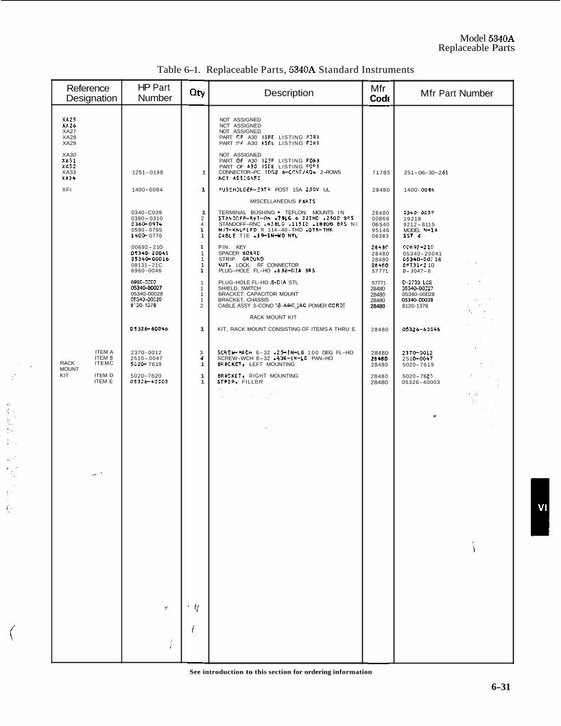
Model 5340A Replaceable Parts
Reference Designation
XA25 XA26 XA27 XA28 XA29
XA30 XA31 XA32 XA33 Xb34
XFI
ITEM A ITEM B
RACK ITEMC MOUNT KIT ITEM 0
ITEM E
Table 6-1. Replaceable Parts, 5340A Standard Instruments
HP Part Number
1251- 01 98
1400- 0084
0340-C039 0380-0310 0380-0974 0590-0765 1400- 0776
00692-21 0 05340=20041 05340-00016 08131-21C 6960-0046
8960-0002 05340Mx)27 05340-00028 05340-wO29 8120-1378
0 5 3 2 6 b O Q 4 6
2370-0012 2510- 0047 5020- 761 9
5020-7620 0 5 3 2 6 4 0 0 0 3
- Qh, -
1
1
1 2 4 1 1
1 1 1 1 1
1 1 1 1 2
1
3 4 1
1 1
’ I/
1 I I
-
Description
NOT ASSIGNED NCT ASSIGNED NOT ASSIGNED PART OF A30 ISFE LISTING FOR1 PART flF A30 (SFE LISTING F3RI
NOT ASSIGNED PART OF A30 ISEF LISTING FOR1 PART OF b30 ISFE LISTING FOP1 CONNECTOR-PC FDGE bCDNT1RDW 2-ROWS NOT 4SSIGNFO
FUSEHOLDER-EXTR POST 15A 250V UL
MISCELLANEOUS PARTS
TERMINAL BUSHING - TEFLON: MOUNTS I N STANDOFF-RVT-ON -75LG 6-32THO - 2 5 0 C BRS STANDOFF-RNC -438LG .115ID .18eUO 8RS N I NIJT-KNURLFD R 114-40-THD -07R-THK CA8LE T I E .19-1N-WO N I L
PIN. KEY SPACER BOAR0 STRIP. GROUND NUT. LOCK. RF CONNECTOR PLUG-HOLE FL-HO -688-DIA BRS
PLUG-HOLE FL-HO . 5 0 I A STL SHIELD, SWITCH BRACKET. CAPACITOR MOUNT BRACKET, CHASSIS CABLE ASSY 3-COND 18-AWGjAC POWER CORD1
RACK MOUNT KIT
KIT, RACK MOUNT CONSISTING OF ITEMS A THRU E
SCREM-PACH 6-32 -25-IN-LG 1 0 0 DEG FL-HO SCREW-WCH 8-32 -438-IN-LG PAN-HO BRACKETt LEFT MOUNTING
ERACKETW RIGHT MOUNTING STPIP. FILLER
- Mf r Cod€ -
71785
28480
28480 00866 06 540 95146 06383
2 8 4 ~ 28480 28480 28480 57 77 1
57771 28480 28480 28480 28480
28480
28480 28480 28480
28480 28480
-
Mfr Part Number
251- 06- 30-2 61
1400- 0084
0340-0039 19218 9212- 81 15 MODEL N-1A SST 4
OCh92-210 05340- 20041 C.5340-30: 16 Ofl731-2 10 D- 3 047- 8
D-2733- LCS 05340-00027 05340-00028 05340-00029 8120-1378
05326-6004b
2370-0012 251 0-0047 5020- 7619
5020-76 20 05326-40003
See introduction to this section for ordering information
6-31
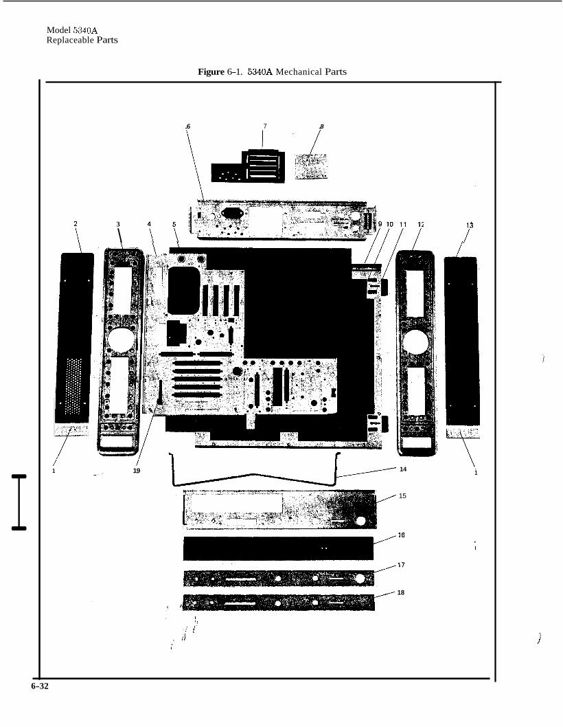
Model 5340A Replaceable Parts
I
Figure 6-1. 5340A Mechanical Parts
6 7 8
P 3
\ \ \
1 14 / I 1 19
15
18
I ' , i i
, iJ I
6-32
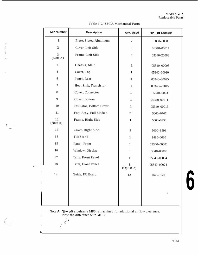
Model 5340A Replaceable Parts
Table 6-2. 5340A Mechanical Parts
,
MP Number
1
2
3 (Note A)
4
5
6
7
8
9
10
11
12 (Note A)
13
14
15
16
17
18
19
Description
Plate, Fluted Aluminum
Cover, Left Side
Frame, Left Side
Chassis, Main
Cover, Top
Panel, Rear
Heat Sink, Transistor
Cover, Connector
Cover, Bottom
Insulator, Bottom Cover
Foot Assy, Full Module
Frame, Right Side
Cover, Right Side
Tilt Stand
Panel, Front
Window, Display
Trim, Front Panel
Trim, Front Panel
Guide, PC Board
Qty. Used
2
1
1
1
1
1
1
1
1
1
5
1
1
1
1
1
1
1 (Opt. 002)
13
HP Part Number
5000-0050
05340-00014
05340-20068
05340-00003
05340-00010
05340-00025
05340-20045
05340-0023
05340-00011
05340-00013
5060-0767
5060-0730
5000-8593
1490-0030
05340-00001
05340-00005
05340-00004
05340-00024
5040-0170
Note A: The bf t sideframe MP3 is machined for additional airflow clearance. Note the difference with MP12.
, !I 1 ' i l
I
6
6-33
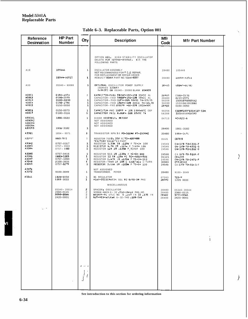
Model 5340A Replaceable Parts
Reference Desi nna ti on
A 1 8
A 3 3
A 3 3 C 1 A33C2 A 3 3 C 3 A 3 3 C 4 A 3 3 C 5
h33C6 A 3 3 C 7
A 3 3 C R 1 A33CRZ A 3 3 C R 3 A 3 3 C R 4 A 3 3 C R 5
A 3 3 P 1
A33R1.
A 3 3 R 2 A 3 3 R 3 A 3 3 R 4
A33R5 A 3 3 R 6 A 3 3 R 7 A 3 3 R 8 A 3 3 1 9
A 3 3 T 1 A 3 3 7 2
A 3 3 U 1
HP Part Number
1 0 5 4 4 A
l O 5 4 k - 6 0 5 1 1
0 5 3 4 0- 6 0 0 8 0
0 1 8 0 - 2 3 7 3 0 1 8 0 - 2 3 7 3 0180-0230 0 1 8 0 - 1 7 4 6 0150-0050
0150-0073 0 180-01 16
190 6-00 21
190 1.. 31 82
1 8 5 4- 0 0 7 1
0683-751 5
0 757-0 31 7 0 7 5 7- 0 9 4 0 0 7 5 7- 0 9 50
0757-0416 0 68 3-1205 0 757- 1094 2 100- 2633 0 75 7- 0279
9100-3049
1826-0010 1205 0033
0 5 3 4 0- 2 0 0 1 4 2360-0115 3050-0066 2420-0001
Table 6-3. Replaceable Parts, Option 001 - QtY -
1
1
1
2
1 1 1
1 1
1
1
1
1
1 1 1
1 1 1 1 1
1
1 1
2 2 2 2
I ? I i
i 1
!I -
Description
O P T I O N 0019 H I G H S T A B I L I T Y D S C I L L A T D P D E L E T E A 1 8 l O 5 3 4 C - 6 1 0 3 6 1 . A 0 0 THE FOLLOWING PARTS:
OSCILLATOR ASSEMBLY NOT RECOMMENDED FOR F I E L D REPAIR, FOR REPLACEMENT OR REPAIR ORDER R E B U I L T 10544A P A R T NO. 10544-80511
O P T I O N A L O S C I L L I T O R POWEP SUPPLY ( S E R I E S 1 2 3 6 A ) (LOADED ON 0 5 3 4 0- 2 0 0 8 0 BLANK 8CI4RO)
CAPACITOR-FXO: 580UF+150-1 f lX 35VOC AL CAPACITOR- FXOI 580UF+150-1OX 35VOC A L C A P A C I T O R- F X O I l U F C Z O I , JOVDC T A - S O L I Q CAPACITOR- FXOI 1 5 U F + - l O X ZOVDC T I - S O L I D CAPACITOR- FXO lOOOPF +80-20X lOOOWVOC
CAPACITOR.=FXO l O D P F C l O X lOOOWVOC CEF CAPACITOR.-FXO; 6 .8UF+-101 35VQC TA
D I O D E A S S E M ~ L Y I BRIDGE NOT A S S I G N E D NOT A S S I G N E D NOT A S S I G N E D
T R A N S I S T O R N P N SI PD=3OORW FT=Z(IORHZ
RESISTOR 7 5 0 5% .25W FC TC=-4D0/+800 * F A C T O R Y S E L E C T E D P A R T RESISTOR 1.33K 1Z - 1 2 5 U F TC=O+ 100 R F S I S T O R 4.7K 2% . 1 2 5 U F T C = O c 1 0 0 R E S I S T O R 1 2 K 2 X .125W F ,TC=O+ 100
R E S I S T O R 511 1 X -125W F T C - 0 + - 1 0 0 R E S I S T O R I2 5 1 -2SW FC T C - * 4 0 0 / + 5 0 0 R E S I S T O R 1.47K 1 X -125W F T C = 0 + - 1 0 0 RESISTOR- TRMR I K 101 C S I D E - A O J 1 - T U R N RESISTOR 3.16~ i x .i25n F TC=O+ IOO
NOT A S S I G N E D TRANSFORMER, POYER
IC REGULATOR HEAT='OISSIPATOR SGL T 0 - 5 / T 0 - 3 9 PKG
MISCELLANEOUS
SPACER P O S C I L L A T O R SCREW-MACH 6- 3 2 - 3 1 2 - I W L G PAN-HO WASHFR-FL U T L C NO. 6 -147 I N ID . 3 7 5 I N NUT-HEX-W/LKYR 6- 32- THD .109-THK
- Mf r Cod€ -
2 8 4 8 0
2 8 4 8 0
2 8 4 8 0
za4m 2 8 4 8 0 5 6 2 0 9 5 6 2 8 9 2 8 4 g O
5 6 2 5 6 5 6 2 8 9
0 4 7 1 3
28400
20480
01121
2 4 5 4 6 2 4 5 4 6 2 4 5 4 6
24546 01121 2 4 5 4 6 30983 2454b
28480
0 7 2 6 3 284 f lO
2 8 4 8 0 2 8 4 8 0 2 8 4 8 C 2 8 4 8 0
-
Mfr Part Number
1 0 5 4 4 6
1 0 5 4 4 . 6 0 5 1 1
(1534r l -6L I80
0 1 8 0 - 2 3 73 0 1 8 0 - 2 3 7 3 15001 0 5 X 0 0 5 D A 2 1 5 0 0 1 56 X902 062 0150-0050
C 0 2 8 0 1 0 2 F l O l K S 2 7 - C O H 1 SOD 6 8 5 X 9 0 3 5 R2
U D b 9 2 2 - 6
1901-3182
1 8 5 4 - 0 G 7 1
CB7515
C + l / B , T O - 1 3 3 1 - F C 4 - 1 / 8 ~ T O - 4 7 0 1 - 6 C 4 - 1 / 8 - T 0 - 1 2 0 2 -G
C 4 1 1 9 . T O - 5 1 1 R - F C 8 1 2 0 5 C 4 - 1 / 8 - T O = 1 4 7 1 - F E T 5 0 X 1 0 2 C4- 1 / 8 - T O - 3 16 1- F
9 1 0 0 - 3 0 4 9
7 2 3 H M 1205 0033
0 5 3 4 0 - 2 0 0 4 4 2360-01 15
242 0 - 00 01 ~ C ~ S - O M ~
See introduction to this section for ordering information
6-34
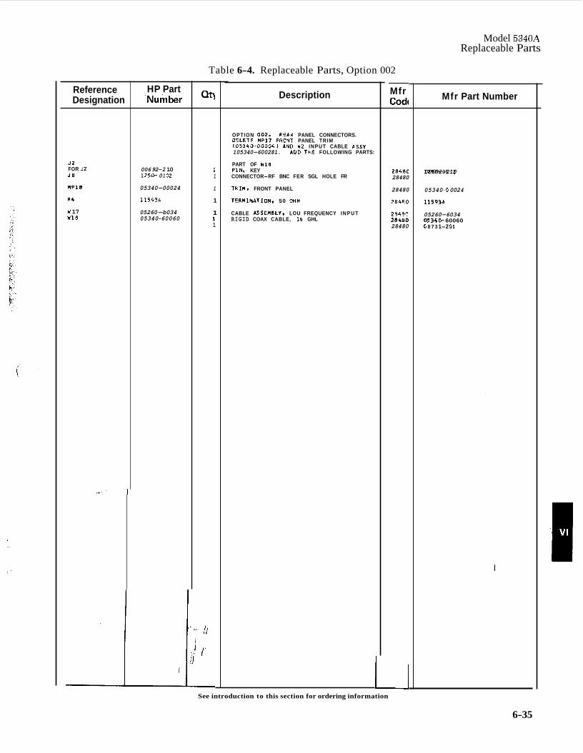
Model 5340A Replaceable Parts
Reference Designation
5 2 FOR J2 J 8
UP18
a4
W 17 W18
HP Part -Number
006 92- 2 10 1 250- 0 1 92
05340-00024
11593A
05260-b034 05340-60060
I
' ,,
i
Table 6-4. Replaceable Parts, Option 002
i 1
1
1
1 1 1
I / I I
:I / ' il
Description
OPTION 002 . R f 4 d PANEL CONNECTORS. DELETE RP17 F R O W PANEL TRIM (0534-000041 AN0 U2 INPUT CABLE LSSY - .. 105340-600281. A00 THT- FOLLOWING PARTS:
PART OF W18 P I N , KEY CONNECTOR-RF BNC FER SGL HOLE FR
TRIM. FRONT PANEL
TFRMINATION. 50 OHM
CABLE ASSEM8LY. LOU FREQUENCY I N P U T RIGID COAX CABLE, 18 GHL
- Mfr Codc
2848C 28480
28480
28480
2948Q
28480 28480
Mfr Part Number
00692-210 izsn-aio2
05340 -0 002 4
1 1 5 9 3 6
05260-6034 05340,- 60060 G 8 7 3 1-2 01
See introduction to this section for ordering information
6-35
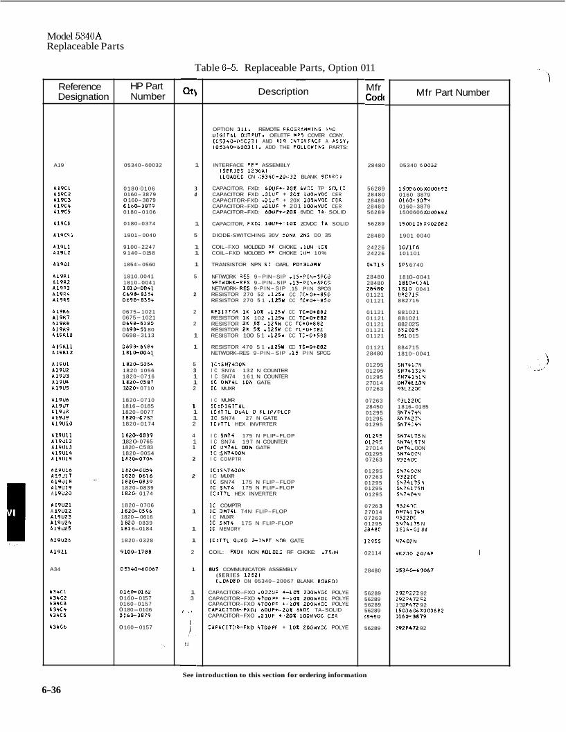
Model 5340A Replaceable Parts
Reference Designation
A19
A19C1 A19C2 A19C3 A19C4 Al9C5
A19C6
A19CR1
A19L1 A19L2
A19Pl
A19Rl A19R2 A19R3 A19R4 A19R5
A19R6 A19R7 A19R8 A19R9 A19R10
A 1 9 R l l A19Rl2
A19Ul A19UZ A19U3 A l 9 M A19U5
A19U6 A19U7 A19U8 A19U9 A19U10
A 1 9 U l l A19U12 A19U13 A19U14 A19U15
A19U16 A19U17 _ _ A19U18 A19U19 A 19U20
A19U21 A 19U22 A19U23 A19U24 A19U25
A19U26
A1921
A34
A34C1 A34C2 A34C3 A34C4 A34C5
134C6
HP Part Number
05340-60032
0 1 8 0 -0 1 0 6 0160- 3879 0 160-3879 0160-3879 0180- 0106
0180- 0374
1901- 0040
9100- 2247 9 140- 01 58
1854-0560
1810.0041 1810- 0041 181C-0041 0698-8354 0698-8354
0675- 1021 0675- 1021 0698-5180 0 698-51 80 0698-3113
0698-6984 1810-0041.
1820-0054 1820 1056 1820- 0716 1820-0587 1 820 ; 0710
1820- 0710 1816-0185 1820-0077 1820-0782 1820- 0174
1820,0839 1 82 0- 0765 1820-C 5 83 1820-0054 1820-0706
1820-0054 1820-0616 1820-0839 1820- 0839 182C- 0174
1820- 0706 1820-0596 1820-0616 1 8 2 0 0839 1 8 1 6-01 84
1820- 0328
9100-1788
05340-60067
O lq0-0162 0 160- 01 57 0160- 0157 0 180-0106 0160-3879
0 160-0157
Table 6-5. Replaceable Parts, Option 011
1
3 4
1
5
1 1
1
5
2
2
2
1
1
5 3 1 1 2
1 1 1 2
4 1 1
2
2
1
1
1
2
1
1 3
I I ,
1 1
t i 1 :
-
~~
Description
OPTION 011. REMOTE PCOGR4MMIMC 4NC DIGITAL OUTPUT, OELETF MPR COVER CONY. lC5340-0OC231 AND P I 9 INTEQFPlCE A PSSYt 105340-600311. ADD THE FDLLOllNG PARTS:
INTERFACE "8" ASSEMBLY ISERIES 1236Al ILOADEO CN 0534G-20~32 BLANK 8CbROl
CAPACITOR. FXD: 60UF+-201 6VOC TP SOLIC CAPACITOR FXD .OlUF + 201 l0OWVOC CER CAPACITOR-FXD -01UF + 20X 1OOUVOC CEH CAPACITOR-FXD .OlUF + 201 lOOWVDC CER CAPACITOR-FXD: 6OUF+-ZOX 6VDC T i - SOLID
CAPACITOR, FXD: lOUF+-104 ZOVDC T I SOLID
DIODE-SWITCHING 30V 50NA ZNS DO 35
COIL-FXO MOLDED 9 F CHOKE .1UH 102 COIL-FXD MOLOEO RF CHOKE 1UH 10%
TRANSISTOR NPN SI OARL PO=31JMY
NFTWORK RES 9-PIN-SIP .lS-PIN-SPCG NETYDRK-RES 9-PIN-SIP -15-PIN-SPCG NETWORK- RE5 9 -P IN- SIP .15 P IN SPCG RESISTOR 270 52 .125W CC TC=O+-850 RESISTOR 270 5 1 -125W CC TC*0+-850
RESlSTOR 1K 10X .125W CC T C 4 + 8 8 2 RESISTOR 1 K 102 .125U CC TC*O+EBZ RESISTOR 2K 5X .125W CC TC-O+882 RESISTOR 2K 5X -125W C C TC*O+982 RESISTOR 100 5 1 -125U CC TC-0+588
RESISTOR 470 5 1 .125Y CC TC=O+882 NETWORK-RES 9-PIN- SIP -15 P I N SPCG
IC:SN7400N I C SN74 132 N COUNTER I C SN74 1 6 1 N COUNTER I C OM74L ION GATE I C MUXR
I C MUXR 1C:OIGITAL 1C:TTL DUAL D FLIPlFLOP IC SN74 27 N GATE 1C:TTL HEX INVFRTER
I C SN74 175 N FLIP-FLOP I C SN74 197 N COUNTER I C OM74L Doh GATE I C : S N7400N I C COMPTR
ICZSN7400N I C MUXR I C SN74 175 N FLIP-FLOP I C SN74 175 N FLIP-FLOP 1C:TTL HEX INVERTER
I C COMPTR I C OM74L 74N FLIP-FLOP I C MUXR I C SN74 175 N FLIP-FLOP I C MEMORY
1C:TTL QUA0 2-INPT NOR GATE
COIL: FXOi NON MOLDED RF CHOKE: .75UH
BUS COMMUNICATOR ASSEMBLY ( S E R I E S 12521 (LOAOEO ON 05340- 20067 BLANK BOARD1
CAPACITOR-FXO -022UF + - l o g 2OOYVOC POLYE CAPACITOR-FXD 4700PF + - l o 1 ZOOYVDC POLYE CAPACITOR-FXO 4700PF + - l o 1 ZOOWVDC POLYE CAPACITOR-FXDi 60UF+-202 6VDC TA-SOLID CAPACITOR-FXO .OlUF + , 2 0 X lOOWVDC C E R
CAPACITOR.-FXD 4700PF + 1 0 1 ZOOYVDC POLYE
- Mfr Codc -
28480
56289 28480 28480 28480 56289
56289
28480
24226 24226
04713
28480 28480
01121 01121
01121 01121 01121 0 1 1 2 1 01121
01121 28480
01295 01295 01295 2701 4 07263
07263 28450 01295 01295 01295
01295 01295 27014 01 295 07263
01295 07263 01295 01295 01295
07 26 3 27014 07263 01295
2 ~ 4 8 0
281.90
12955
02114
28480
56289 56289 56289 56289 !8480
56289
Mfr Part Number
05340 60032
1500606X000682 0160 3879 0160-3379 0160-3879 1500606 X000682
1500106X902082
1901 0040
10/1rl) 101101
SPS 6740
181 0- 0041 181C-C941 1810 0041 flR2715 882715
881021 881021 882 02'5 882025 881 01 5
884715 1810- 0041
SN740flN Sh174132N SN74161Y
93L22DC
93L22DC 1 8 1 6- 01 85 SN7474N SN7427N SN74C4N
SN74175 N SN74197N OM74L OON SN7400N 9324DC
Slu74CON 9322DC SN74175N SN74175N SN7404N
93240C DM74L74N
SN74175 N 1816-01 84
N7402N
0 ~ 7 4 i i n ~
9 x 2 ~ ~
VKZOO 20/40 I
292P223 92 292P47292 2 '32 P472 92 1500606XOO06RZ >160-317'3
!92P172 92
See introduction to this section for ordering information
6-36
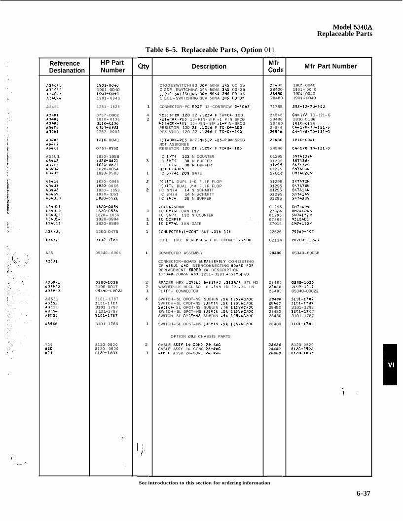
Model 5340A Replaceable Parts
Table 6-5. Replaceable Parts, Option 011
Reference Desianation
A 3 4 C R 1 A34CR 2 A34CR3 A 34CR4
A 3 4 5 1
A 3 4 R 1 A 3 4 R 2 P 3 4 R 3 A34R4 A 3 4 R 5
A 3 4 8 6 A 3 4 R 7 A34118
A 3 4 U 1 A 3 4 U 2 A34U3 A 3 4 U 4 A 3 4 U 5
A 3 4 U 6 A 3 4 U 7 A 3 4 U 8 A 3 4 U 9 A 3 4 U 1 0
A 3 4 U 1 1 A 3 4 U 1 2 A 3 4 U 1 3 A 3 4 U 1 4 A 3 4 U 1 5
A 3 4 X U 1
A 3 4 L l
A 3 5
A 3 5 1 1
A35MP1 P 3 5 M P 2 A35MP3
A 3 5 5 1 A 3 5 5 2 A 3 5 5 3 A 3 5 5 4 A 3 5 5 5
A 3 5 5 6
Y 1 9 Y 2 0
HP Part Number
1901-0040 1901-0040 19U1-004C 1 9 0 1 - 0 0 4 0
1 2 5 1- 1 6 2 6
0 7 5 7- 0902 1 8 1 0- 0 1 3 6 1 81 0-Cl36 0 757-C902 0 7 5 7 - 0 9 0 2
l 8 l D 0041
0 7 5 7- 0 9 C 2
1 8 2 0- 1056 1820-0621 1820-ce21 1820- 0054 1820- 0 5 8 0
1 8 2 0- 0 0 6 5 1 8 2 0 - 0 0 6 5 1 8 2 0- 1 0 5 3 1 8 2 0 - 1 053 1 8 2 0 - 0 6 2 1
1820-0054 1 8 2 0 - 0 5 8 6 1 8 2 0- 1 0 5 6 1820-0904 1820-0589
1200-0475
9 1 0 0 - 1 7 8 8
0 5 3 4 0- 6 0 0 6
0380-1036 2190-0017 0534C-GOO22
3 1 0 1- 1 7 8 7 3 1 0 1 - 1 7 8 7 3101 1 7 8 7 3 10 1- 1 7 8 7 3101-1787
3101 1788
8120- 0 5 2 0 8 1 2 0 - 0 5 2 0 8 1 2 0 - 1 833
I
1
4 2
3
1
2
2
1
1 1
1
1
2 2 1
5
1
2
1
I 1.
-
Description
O I O D E S W I T C H I N G 3OV 50NA ZNS OC 35 CIODE- SWITCHING 3 0 V 50NA ZNS 00-35 CIODE-SWITCHING 3 0 V 5nNA 2NS 00 3 5 CIOOE- SWITCHING 30V 50NA 2NS 00-35
CONNECTOR-PC EOGt 12-CONTIROW 2-POWS
RESISTOR 120 2 Z -125W F T C c O t 100 NETWCRK.-RES 1 0 - P I N - S I P -1 P I N SPCG NETWORK-RES 10- PIN- SIP -1-P IN-SPCG PESISTOR 120 22 -125W F TC=O+-lOO RESISTOR 120 22 .125W F TC=O+-lOO
hETWORK-RES 9 - P I N - S I P .15-PIN= SPCG NOT ASSIGNEE RESISTOR 120 2% .125W F TC=O+-100
I C S N 7 4 132 N COUNTER I C S N 7 4 38 N BUFFER I C S # 7 4 38 ’4 BUFFER I C :S N 7 4 0 0 N I C OW74L ZON GATE
1C:TTL OUPL J-K F L I P FLOP 1C:TTL DUAL J--K F L I P FLOP I C S N 7 4 14 N SCHMITT I C S N 7 4 14 N SCHMITT I C S N 7 4 38 N BUFFER
1 C :S N74OON I C OM74L 0 4 N I N V I C S N 7 4 1 3 2 N COUNTER I C COUPTR I t DW74L 3 0 N GATE
CONNECTOR:l-CONT SKT - 0 1 6 D I A
C O I L : FXO; hCN-MOLCED RF CHOKE; - 7 5 U H
CONNECTOR ASSEMBLY
CONNECTOR-BOAR0 SUBASSEM8LY C O N S I S T I N G OF A 3 5 J 1 AN0 INTERCONNECTING BOARD F’JR REPLACEMENT ORDER BY DESCRIPTION ( 3 5 3 4 0 - 2 0 0 6 6 AND 1 2 5 1- 3 2 8 3 ASSEM8L €0.
SPACER-HEX - 2 5 5 L G 6-32THO - 3 1 2 A I F STL N 1 WASHER-LK HLCL NO. 8 - 1 6 8 I N I 0 -31 I N PLATE, CONNECTOR
SWITCH-SL OPOT-NS SUBHIN .5A 1 2 5 V A C I O C SWITCH- SL CPOT-NS SUSHIN .5P 1 2 5 V A C I n C S N I T C W S L OPOT-NS SUBUIN .5A 125VAC/DC SWITCH-SL DPCT-NS SUBMIN .5A 1 2 5 V A C I D C SWITCH-SL CPOT-NS SUBRIN .5A 125VACIOC
SWITCH-SL OPST-NS SUBMIN - 5 P 1 2 5 V A C I D C
OPTION 003 CHASSIS PARTS
CABLE PSSY I C C O N O Z b - 4 Y G CABLE ASSY 14-CON0 26-AUG CABLF ASSV 24-CONE 24-AYG
- Mfr Cod€
284RO 28400
28480
71785
2 4 5 4 6 28480 2 8 4 8 0 2 4 5 4 6 24546
2wno
zecao
24546
01295 0 1 2 9 5 91295 01 2 9 5 27 01 4
01295 01295 01295 01295 01295
0 1 2 9 5 27 01 4 0 1 2 9 5 0 7 2 6 3 27014
22526
02114
28480
2 8 4 8 0 28480 2 8 4 8 0
28480 2848C 28 48 0 28480 28480
28 480
28480 28480 28480
-
Mfr Part Number
190 1- 0040 1 9 0 1- 0 0 4 0 190 1- 0040 1901-0040
252-12-33-300
C + l I 8 TO-121-G 181 0 -01 36 1810-01 3 6 C 4 - 1 / 8 - T I - 1 2 1 -G C 4 - 1 1 8 - T O - 1 2 1 4
1 8 1 0 - 0 0 4 1
C + l M - T O - 1 2 1 *G
S N 7 4 ? 3 2 N SN7430N SN743RN SN7400N OU74LZON
S N 7 4 7 0 N S N 7 4 7 0 N SN7414N SN7414N SN7438N
SN74OON D U 7 4 L 0 4 N S N 7 4 1 3 2 N 9 3 L 2 4 0 t OM74L30N
75C60-705
V K 2 0 0 - 2 0148
05340-60068
0380-1036 219O-G317 05340-00022
3101-1787
3 1 01- 17 8 7 31ql-17 0 7 3101- 1787
3 1 0 1 - 1 7 0 8
31121- 1737
8120- 0 5 2 0 812G-CS21 8120-1833
See introduction to this section for ordering information
6-37
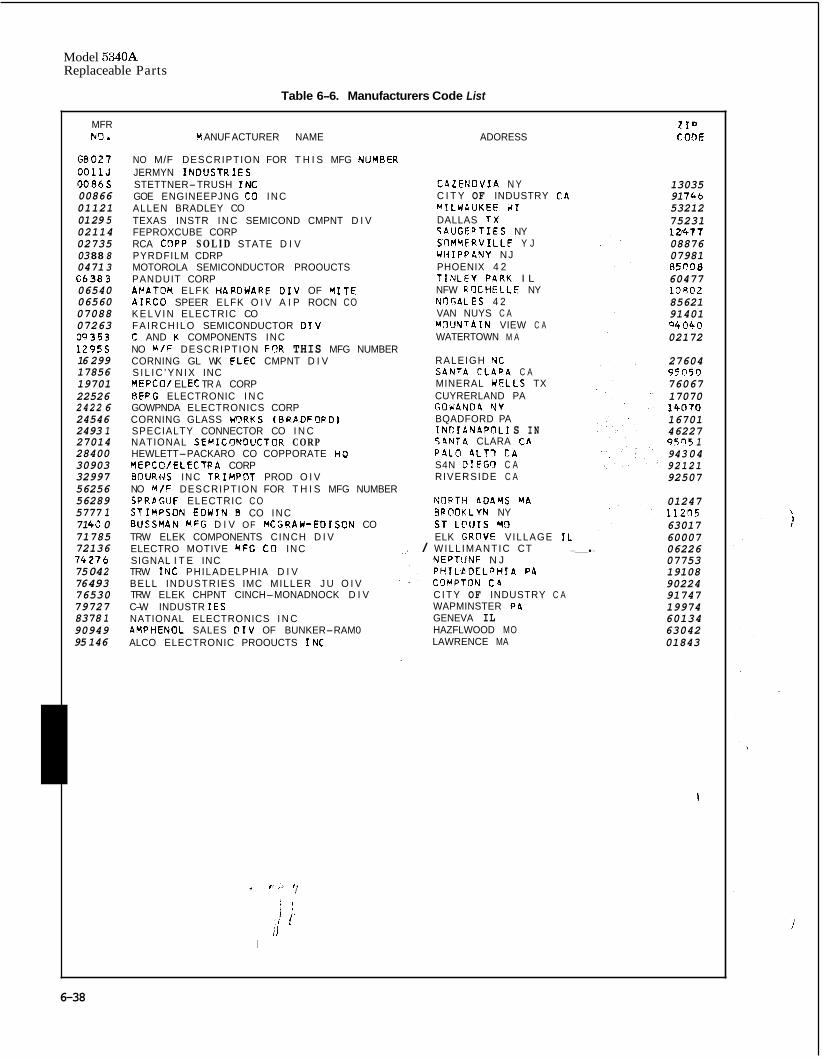
Model 5340A Replaceable Parts
I
Table 6-6. Manufacturers Code List
MFR NO.
60027 OOllJ 00865 00866 01121 01 29 5 02114 02735 03 88 8 0471 3 C6383 06540 06560 07088 07263 09353 12955 16 299 17856 19701 22526 2422 6 24546 2493 1 27014 28400 30903 32997 56256 56289 5777 1 71 4C 0 71785 72136 74276 75 04 2 76 49 3 76530 79727 8378 1 90949 95 146
M ANUF ACTURER NAME
NO M/F DESCRIPTION FOR T H I S MFG NUM0ER JERMYN INOUSTRiES STETTNER-TRUSH IN(; GOE ENGINEEPJNG CO INC ALLEN BRADLEY CO TEXAS INSTR I N C SEMICOND CMPNT D I V FEPROXCUBE CORP RCA CDPP S O L I D STATE D I V PYRDFILM CDRP MOTOROLA SEMICONDUCTOR PROOUCTS PANDUIT CORP AHATOM ELFK HARDYARE D I V OF M I T E 4 IRCO SPEER ELFK O I V A I P ROCN CO K E L V I N ELECTRIC CO FA IRCHILO SEMICONDUCTOR O I V t AND K COMPONENTS INC NO M/F DESCRIPTION FOR THIS MFG NUMBER CORNING GL WK FLEC CMPNT D I V S I L I C ’ Y N I X INC MEPCO/ EL EC TR A CORP BERG ELECTRONIC I N C GOWPNDA ELECTRONICS CORP CORNING GLASS UDRKS (BRADFORD) SPECIALTY CONNECTOR CO I N C NATIONAL SEMICONOUCTQR CORP HEWLETT-PACKARO CO COPPORATE HO MEPCO/ELECTPA CORP BOURiJS INC TRIHPf lT PROD O I V NO M/F DESCRIPTION FOR T H I S MFG NUMBER SPRbGUE ELECTRIC CO STIMPSON EDWIN 6 CO INC BUSSMAN MFG D I V OF MCGRAW-EDISON CO TRW ELEK COMPONENTS CINCH D I V ELECTRO MOTIVE YFC C9 INC SIGNAL I T E INC TRW I N C PHILADELPHIA D I V BELL INDUSTRIES IMC MILLER J U O I V TRW ELEK CHPNT CINCH-MONADNOCK D I V C-W INDUSTR 1ES NATIONAL ELECTRONICS I N C AMPHENOL SALES D I V OF BUNKER-RAM0 ALCO ELECTRONIC PROOUCTS 1NC
1 1
1. I
ADORESS
C4ZENOVIA N Y C I T Y OF INDUSTRY C 4 MILWCIUKEE W I DALLAS TX SAUGEPTIES NY SCIMYERVILLE Y J WHIPPCNY NJ PHOENIX 4 2 T INLEY P4RK I L NFW RQCHELLE NY NOGALES 4 2 VAN NUYS C A YOUVTAIN VIEW C A WATERTOWN M A
RALEIGH Y C SANTA CLARA C A MINERAL UELLS TX CUYRERLAND PA GOWAND4 Y Y BQADFORD PA INPIANAPflLI S I N 5 4 N T A CLARA CA
S4N DTFGCI C A RIVERSIDE C A
P A L O ALTI r 4
NOPTH A04YS M A BRClOKLYN NY ST LC’IJTS Y 9 ELK GROVE VILLAGE I1
/ WILL IMANTIC CT -_I-
NEPTIJNF N J PH ILbDELpHIA P4 CCIMPTON t 4 C I T Y OF INDUSTRY C A WAPMINSTER P4 GENEVA IL HAZFLWOOD MO LAWRENCE MA
ZIP CODE
13035 91 766 53212 75231 12417 08876 07981 0 5 C O B 60477 10802 85621 91401 94040 02172
27604 95050 76067 17070 16070 16701 46227 95n5 1 94 3 04 92121 92507
01247 11205 63017 60007 06226 07753 19108 90224 91747 19974 60134 63042 01843
II
6-38
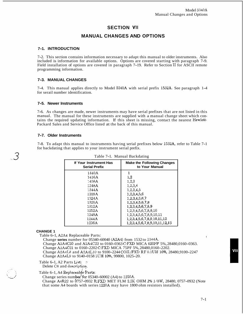
Model 5340A Manual Changes and Options
.". 3
SECTION VII
MANUAL CHANGES AND OPTIONS
7-1. INTRODUCTION
7-2. This section contains information necessary to adapt this manual to older instruments. Also included is information for available options. Options are covered starting with paragraph 7-9. Field installation of options are covered in paragraph 7-19. Refer to Section I1 for ASCII remote programming information.
7-3. MANUAL CHANGES
7-4. This manual applies directly to Model 5340A with serial prefix 1532A. See paragraph 1-4 for serail number identification.
7-5. Newer Instruments
7-6. As changes are made, newer instruments may have serial prefixes that are not listed in this manual. The manual for these instruments are supplied with a manual change sheet which con- tains the required updating information. If this sheet is missing, contact the nearest Hewlett- Packard Sales and Service Office listed at the back of this manual.
7-7. Older Instruments
7-8. To adapt this manual to instruments having serial prefixes below 1532A, refer to Table 7-1 for backdating that applies to your instrument serial prefix.
Table 7-1. Manual Backdating -~ ~~ ~
If Your Instrument Has Serial Prefix
1440A 1416A 1408A 1348A 1344A 1328A 1324A 1320A 1312A 1252A 1248A 1244A 1236A
Make the Following Changes to Your Manual
1 172 1,273 132,394 1,293,495 1,2,3,4,5,6 1,2,3,4,5,6,7 1,2,3,4,5,6,7,8 1,2,3,4,5,6,7,8,9 1,2,3,4,5,6,7,8,9,10 1,2,3,4,5,6,7,8,9,10,11 1,2,3,4,5,6,7,8,9,10,11,12 1,2,3,4,5,6,7,8,9,10,11,12,13
CHANGE 1 Table 6-1, A2A4 Replaceable Parts:
Change series number for 05340-60040 (A2A4) from 1532 to 1344A. Change A2A4C20 and A2A4C22 to 0160-0363 C:FXD MICA 620PF 5%, 28480,0160-0363. Change A2A4C21 to 0160-2202 C:FXD MICA 75PF 5%, 28480,0160-2202. Change A2A4L8 and A2A4L10 to 9100-2244 CO1L:FXD RF O.1UH lo%, 28480,9100-2247 Change A2A4L9 to 9140-0158 1UH lo%, 99800, 1025-20.
' 1
Delete C8 and descriptipn. Table 6-1, A2 Parts List:
Table 6-1, A4 Replaceabie @arts: Change series num ei'for 05340-60002 (A4) to 1220A. Change A4R22 to 6" 757-0932 R:FXD MET FLM 2.2K OHM 2% 1/8W, 28480, 0757-0932 (Note that some A4 boards with series 1220A may have 1800 ohm resistors installed).
7-1
Model 5340A Manual Changes and Options
Table 6-1, A14 Replaceable Parts: Change series number for 05340-60011 (A14) to Series 1236A. Change A14R1 and A14R2 to 0757-0893 RFXD FLM 51 OHM 2% 1/8W, 28480, 0757-0893.
Page 8-13, Figure 8-8, A2 Schematic Diagram: Change A2A4C20 and A2A4C22 to 620PF. Change A2A4C21 to 74PF. Change A2A4L8 and A2A4L10 to O.1UH. Change A2A4L9 to 1UH. Change series number at top of schematic for A2A4 to Series 1220A. Delete C8.
Change A4R22 to 2200 OHMS. Change series number a t top of schematic to Series 1220A.
Change A14R1 and A14R2 to 51 OHMS. Change series number at top of schematic to Series 1236A.
Page 8-17, Figure 8-10, A4 Schematic Diagram:
Page 8-37, Figure 8-20, A14 Schematic Diagram:
CHANGE 2 Page 6-6, A2A3 Parts List:
Change A2A3R1 to 0757-0963 RFXD FLM 43K OHM, 2%, 1/8W, 28480,0757-0963.
Page 8-13, Figure 8-8: Change A2A3R1 to 43K.
Page 6-32, A33 Parts List: Change A33CR1 to 1901-0027, Diode:Silicon 0.75A 400PIV, 04713, SR1358-9. Add A33CR2, CR3, CR4; 1901-0027, Diode:Silicon 0.75A 400PIV, 04713, SR1358-9. Change part number of T2 to 9100-3021.
Page 8-77, Figure 8-35, A33 Power Supply: Replace schematic and component locator with Figure 7-9 and 7-10.
CHANGE 3 Table 6-1, A17 Replaceable Parts:
56289,150D226X9015B2.
2OVDC TA, 56289,150D225X9020A2.
Change A17AlC1 and C2 to 0180-0228, Capacitor; FXD 22 UF *lo% 15VDC TA-SOLID,
Change A17AlC5 through C7, C11, C12 to 0180-0197, Capacitor; FXD 2.2 UF +-lo% Change A17AlL3 to 9140-0158, Coil, FXD, Molded RF Choke, 1 UH lo%, 24226, 10/101. Change A17AlR1 to 0698-5426, Resistor 10K lo%, .125W CC Tubular, 01121, BB1031. Change A17AlR14 to 0698-5996, Resistor 560 OHM 5% .125W CC Tubular, 01121, BB5615. Add A17AlE1, E3, 9170-0029, Core Magnetic, Shielding Bead, .1380D .047, 02114,
Change A17A1 board series number to Series 1320A.
Change A17AlCl and C2 to 22 UFD. Add A17AlC21 2.2 PF from U5B pin 11 to ground. Change A17AlR1 to 10K ohms. Change A17AlR14 to 560 ohms. Delete C22 and C23. Change A17A1 board series number to 1320A.
56-590-65A2/4A.
Figure 8-23, A17 Schematic Diagram:
CHANGE 4 Table 6-1, A13 Replaceable Parts:
Change A13 board series oumber to 1220A. Delete A13R39 and description. Change A13R3 to 0757-08/24 R:FXD FLM 56 ohm 2% 1/8W 28480 0757-0894.
Change A13R3 to 56' ohms. Delete A13R39, connect C4 directly to U1A pin 1.
Figure 8-19, A13 Schemadic Diagram:
7-2
Model 5340A Manual Changes and Options
CHANGE 5 Table 6-1, Replaceable Parts:
Change A3CR5 and CR6 to 1901-0535, Diode:Hybrid Hot Carrier, 28480,1901-0535. Change A20C3 to 0140-0209 C:FXD Mica 5 pfd 5%, 500VDCW, 28480,0140-0209.
Change A20C3 to 5 pfd. Figure 8-27, A20 Schematic Diagram:
CHANGE 6 Table 6-1, Replaceable Parts:
Delete listing for AlA5 (05340-6007) Filter Assy and all associated parts (AlA5A1, etc.). Delete listing for A2A5 (05340-60078) Filter Assy and all associated parts (A2A5A1, etc.).
Delete AlA5 and AlA5A1 from schematic. Show + and -5 volt lines connected directly to AlA2.
Delete A2A5 and A2A5A1 from schematic. Show + and -5 volt lines connected directly to A2A2.
Figure 8-7, A1 Schematic Diagram:
Figure 8-8, A2 Schematic Diagram:
Table 6-1, A6 Replaceable Parts: Change A6 series number 1236A. Change A6R13 to 0757-0938 R:FXD FLM 3.9K ohm 2% 1/8W, 28480,0757-0938. Change A6R15 to 0757-0946 RFXD FLM 8.2K ohm 2% 1/8W, 28480, 0757-0946. Change A6R26 to 0698-8128 RFXD COMP 220 ohm 5% 1/8W, 01121, BB2215. Change A6R27 to 0698-5075 R:FXD COMP 130 ohm 5% 1/8W, 28480, 0698-5075.
Change A6R13 to 3900 ohms, A6R15 to 5600 ohms, A6R26 to 220 ohms, and A6R27 to 130 ohms.
Change A2A4C3 to 0160-2150, C:FXD MICA 33 PF 5%, 28480,0160-2150. Change A2A4R4 to 0757-0180, RFXD MET FLM 31.6 ohm 1% 1/8W, 28480,0757-0180. Change A2A4 board series number to 1220A.
Figure 8-12, A6 Schematic Diagram:
Table 6-1, A2 Replaceable Parts:
CHANGE 7 Table 6-1, A10 (05340-60008) Parts List
Change Series No. to 1252A Change AlOR8 to 0698-4433 RFXD 2260 OHM 1% 1/8W, 28480, 0698-4433 Delete A10R25 and description
Table 6-1, A22 (05340-60016) Parts List Change Series No. to 1236A Change A22Q13 to Q16 to 1854-0009 Change A22R36 to R39 to 0683-6215 620 ohms Change A22R30 to to 0683-3305 R:FXD COMP 330 OHM 5% 1/4W, 01121, CB33056 Change A22Q17 to 1854-0092 Delete A22Q21, A22R54, and A22R55 and their descriptions Change A22U9 to 5088-7001
Figures 8-16 and 8-18 A10 and A12 (05340-60008) schematics: Change A10R8 to 2260 ohms. Change A10R25 200 ohm potentiometer (L2, C5, and R8 are tied together).
Change series no. to 1236A Change A22R30 to 33 ohms Change A22R36 to R39 to 2700 ohms Replace component kocator with Figure 7-1 Delete A22Q21, A22R54, and R55
Figure 8-29, A22 Schematic Diagram:
I CHANGE 8 J
Table 6-1, A10 Replaceable Parts: Change AlOC3 to 0160-2671, C:FXD MYLAR O.1pF 5% 80VDCW, 56289, 192P1045R8-PTS Change A10L3 to 9100-2278, CO1L:FXD MOLDED 150 pH lo%, 82142,09-A151K
7-3
Model 5340A Manual Changes and Options
Change AlORl to 0698-3151 RFXD MET FLM 2.87K OHM 1% 1/8W, 28480,0698-3151 Change A10R6 to 0698-3449, R.FXD MET FLM 28.7K OHM 1% 1/8W, 28480,0698-3449 I
Figures 8-16 and 8-18, A10 and A12 Schematics: Change A10C3 to 0.1 pF Change A10L3 to 150 p H Change AlORl to 2870 OHMS Change A10R6 to 28.7K OHMS
CHANGE 9 Table 6-1, A17 Replaceable Parts:
Add A17AlC17, 0180-0197, C:FXD ELECT 2.2 pF 10% BOVDCW, 56289, 150D225X9020A2-
Add Al7AlC21,0160-2327, C:FXD .001 pF
Add A17AlR6, 8, 9,0698-3378 R:FXD 51 OHM 1/8W, 28480,0698-3378 Add A17AlR5,0698-5177 R:FXD 820 OHM 1/8W, 28480,0698-5177 Add A17AlR19,0757-0404 R.FXD FLM 130 OHM 1% 1/8W, 28480,0757-0404 Add A17AlU4, 1820-0753 1C:TTL DIGITAL, 28480,1820-0753
DYS
Add Terminal Post 0360-0474 (2 each)
Change A17AlR10 to 0683-4715, R:FXD COMP 200 OHM 5% 1/4W, 01121, CB4715 Change A17AlR13 to 0698-3378, R:FXD COMP 100 OHM 1/8W, 28480,0698-3378 Change A17AlR14 to 0674-3315, RFXD COMP 330 OHM 5% 1/8W, 28480, 0674-3315 Delete A17AlE1,2,3, 9170-0029 Bead:Ferrite Delete A17AlR23 and description Delete A17AlC21 and description
Replace schematic diagram with Figure 7-2 (A17A1 schematic series 1220A). Replace com- Figure 8-23, A17A1 Schematic and Component Locator:
ponent locator with Figure 7-3.
,) CHANGE 10
Page 5-2, Table 5-1: Change A20 part number to 05340-60018
Table 6-1, A20 assembly: Replace parts list with Table 7-2.
Figure 8-27, A20 Schematic Diagram: Replace schematic diagram with Figure 7-4. Replace component locator with Figure 7-5.
Figure 8-6, 5340A Block Diagram: Change part number of A20 to 05340-60018.
Table 6-1, A22 Parts List Change part number of A22Q13 thru Q16 to “1854-0009”. Change part number of A22R36 thru R39 to “0683-6215,620 ohms.
Table 6-1, Chassis Parts: Delete C3 through C7 Delete L2 thru L6
Figure 8-23, A17 Schematic Diagram: Delete C3 thru C6 and L2 thru L5.
Figure 7-2, A17 Schematic Diagram: Add A17AlC21 0.001 pF, connected from junction of A17AlR19 and C17 to ground.
Table 6-1, A17 Parts List: Change A17AlC21 0160-2327, C:FXD CER 0.001 pF 20% lOOVDCW
Page 4-47, Paragraph 4-229: Change A20 part number,to 05340-60018
CHANGE 11 i :J
a. Replace A10 schematic diagram (Figure 8-16) with Figure 7-6 (series 1220A). Replace A12 schematic diagram (Figure 8-18) with Figure 7-7 (series 1220A). Replace A10 and A12 component locators with Figure 7-8.
7-4
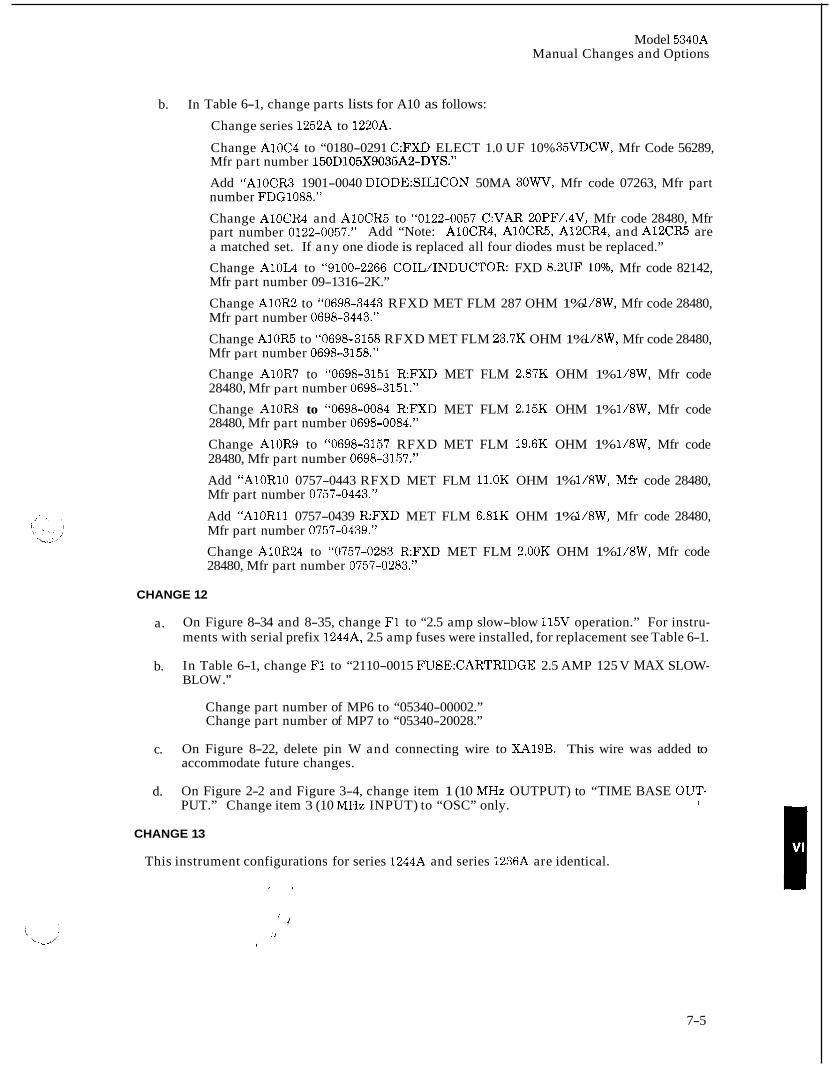
Model 5340A Manual Changes and Options
b. In Table 6-1, change parts lists for A10 as follows:
Change series 1252A to 1220A.
Change A10C4 to “0180-0291 C:FXD ELECT 1.0 UF 10% 35VDCW, Mfr Code 56289, Mfr part number 150D105X9035A2-DYS.”
Add “AlOCR3 1901-0040 DI0DE:SILICON 50MA 30WV, Mfr code 07263, Mfr part number FDG1088.”
Change AlOCR4 and AlOCR5 to “0122-0057 C:VAR 20PF/.4V, Mfr code 28480, Mfr part number 0122-0057.” Add “Note: A1OCR4, AlOCR5, A12CR4, and A12CR5 are a matched set. If any one diode is replaced all four diodes must be replaced.”
Change A10L4 to “9100-2266 COIL/INDUCTOR FXD 8.2UF lo%, Mfr code 82142, Mfr part number 09-1316-2K.”
Change A10R2 to “0698-3443 RFXD MET FLM 287 OHM 1% 1/8W, Mfr code 28480, Mfr part number 0698-3443.”
Change A10R5 to “0698-3158 RFXD MET FLM 23.7K OHM 1% 1/8W, Mfr code 28480, Mfr part number 0698-3158.”
Change A10R7 to “0698-3151 R.FXD MET FLM 2.87K OHM 1% 1/8W, Mfr code 28480, Mfr part number 0698-3151.”
Change A10RE to “0698-0084 R.FXD MET FLM 2.15K OHM 1% 1/8W, Mfr code 28480, Mfr part number 0698-0084.”
Change A10R9 to “0698-3157 RFXD MET FLM 19.6K OHM 1% 1/8W, Mfr code 28480, Mfr part number 0698-3157.”
Add “AlOR10 0757-0443 RFXD MET FLM ll.OK OHM 1% 1/8W, Mfr code 28480, Mfr part number 0757-0443.”
Add “AlOR11 0757-0439 R:FXD MET FLM 6.81K OHM 1% 1/8W, Mfr code 28480, Mfr part number 0757-0439.”
Change A10R24 to “0757-0283 R:FXD MET FLM 2.00K OHM 1% 1/8W, Mfr code 28480, Mfr part number 0757-0283.”
CHANGE 12
a. On Figure 8-34 and 8-35, change F1 to “2.5 amp slow-blow 115V operation.” For instru- ments with serial prefix 1244A, 2.5 amp fuses were installed, for replacement see Table 6-1.
In Table 6-1, change F1 to “2110-0015 FUSE:CARTRIDGE 2.5 AMP 125 V MAX SLOW- BLOW .”
b.
Change part number of MP6 to “05340-00002.” Change part number of MP7 to “05340-20028.”
c. On Figure 8-22, delete pin W and connecting wire to XA19B. This wire was added to accommodate future changes.
On Figure 2-2 and Figure 3-4, change item 1 (10 MHz OUTPUT) to “TIME BASE OUT- PUT.” Change item 3 (10 MHz INPUT) to “OSC” only.
d. I
CHANGE 13
This instrument configurations for series 1244A and series 1236A are identical.
’ 1 ,
I /
. I I
7-5
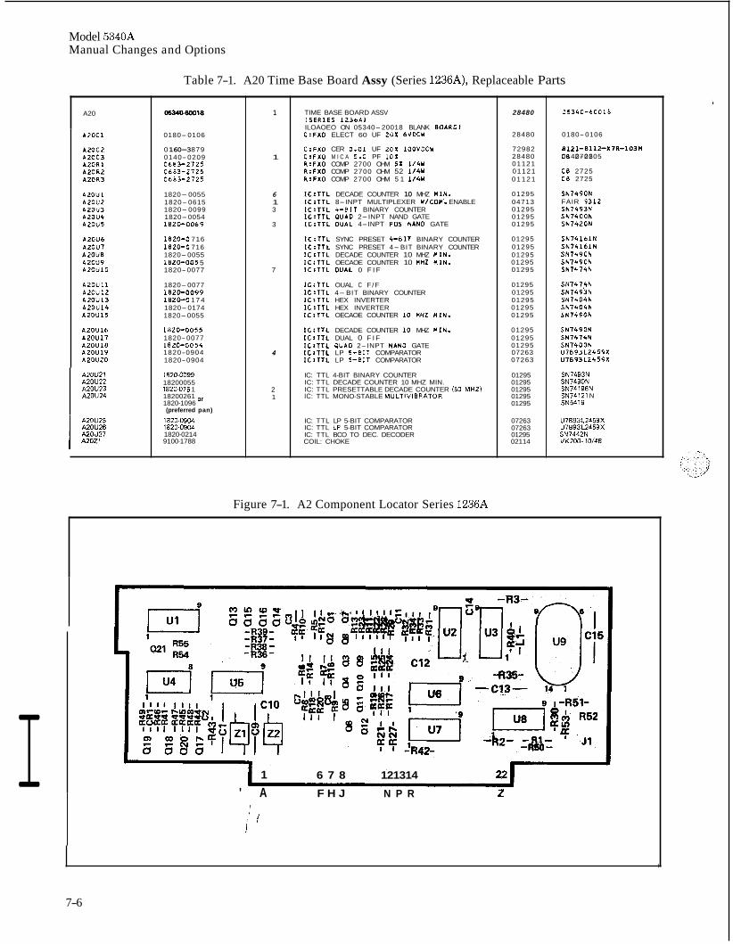
Model 5340A Manual Changes and Options
Table 7-1. A20 Time Base Board Assy (Series 1236A), Replaceable Parts
AZOC1
A20C2 A20C3 A2OR1 AZOR2 A20R3
A20U1 AZOU2 A20U3 A20U4 A20U5
A20U6 A2OU7 A2OU8 A20U9 A2OUlO
A 2 0 U l l A20U12 AZOU13 A20U14 A2OUl5
A2OU16 AZOU17 A20U18 A20U19 A20U20
A20U21 A2OU22 AZOU23 A20U24
A20U25 A20U26 A20U27
A20
0180- 0106
0 160-3 879 0140- 0209 0683-2725 0683-2725 0683-2725
1820-0055 1820- 0615 1820- 0099 1820-0054 1820-0069
1820-0 716 1820-0 716 1820-0055 1820-005 5 1820-0077
1820-0077 1820-0099 1820-0 1 7 4 1820-0174 1820-0055
1820-0055 1820-0077 1820-0054 1820- 0904 1820-0904
1620-0099 18200055 1820-075 1 18200261 1820-1096 Or (preferred pan)
1820-0904 1820.0904 1820-0214 9100-1788
1
1
6 1 3
3
7
4
2 1
TIME BASE BOARD ASSV (SERIES 1236A l ILOAOEO ON 05340-20018 BLANK BOAROI C:FXD ELECT 60 UF 202 6VOCU
C:FXO CER 0.01 UF 201 lOOVOCU C:FXO M I C A 5.0 PF 102 R:FXO COMP 2700 OHM 5 Z 114U R:FXD COMP 2700 OHM 52 114U R:FXO COMP 2700 OHM 5 1 1/4U
1C:TTL DECADE COUNTER 10 MHZ MIN. 1C:TTL 8-INPT MULTIPLEXER UICOM. ENABLE 1C:TTL 4-BIT BINARY COUNTER 1C:TTL QUAO 2-INPT NAND GATE 1C:TTL OUAL 4-INPT POS NANO GATE
1C:TTL SYNC PRESET 4-81T BINARY COUNTER 1C:TTL SYNC PRESET 4-BIT BINARY COUNTER 1C:TTL DECADE COUNTER 10 MHZ MIN. 1C:TTL OECAOE COUNTER 10 HHZ HIN. 1C:TTL OUAL 0 F I F
1C:TTL OUAL C F /F 1C:TTL 4- BIT BINARY COUNTER 1C:TTL HEX INVERTER 1C:TTL HEX INVERTER 1C:TTL OECAOE COUNTER 10 MHZ MIN.
1C:TTL DECADE COUNTER 10 MHZ MIN- 1C:TTL DUAL 0 F I F 1C:TTL QUAO 2-INPT NANO GATE 1C:TTL LP 5-81T COMPARATOR 1C:TTL LP 5-811 COMPARATOR
IC: TTL 4-BIT BINARY COUNTER IC: TTL DECADE COUNTER 10 MHZ MIN. IC: TTL PRESETTABLE DECADE COUNTER (50 M H Z l IC: TTL MONO-STABLE MULTIVIBRATOR
IC: TTL LP 5-BIT COMPARATOR IC: TTL LP 5-BIT COMPARATOR IC: TTL BCO TO DEC. DECODER COIL: CHOKE
28480
28480
72982 28480 01121 01121 0 1 1 2 1
01295 04713 01295 01295 01295
01295 01295 01295 01295 01295
01295 01295 01295 01295 01295
01295 01295 01295 07263 07263
01295 01295 01295 01295 01295
07263 07263 01295 02114
05340-60018
0180-0106
8121-B112-X7R-l03M C 8 0140-0205 2725
CB 2725 C8 2725
SN7490N FAIR 5312 SN7493N SN740GN SN7420N
SN74161N SN74161N SN7490N SN7490N SN7474N
SN747.5N SN7493N SN7404N SN7404N SN7490N
SN7490N SN7474N SN7400N U7893L2459X U7893L2459X
SN7493N SN7490N SN74196N SN74121 N SN5419
U7B93L2459X U7B93L2459X SN7442N VK200- 10/4B
Figure 7-1. A2 Component Locator Series 1236A
I 1 6 7 8 121314 22 ' A F H J N P R z
, ,' / i
'I
I
7-6
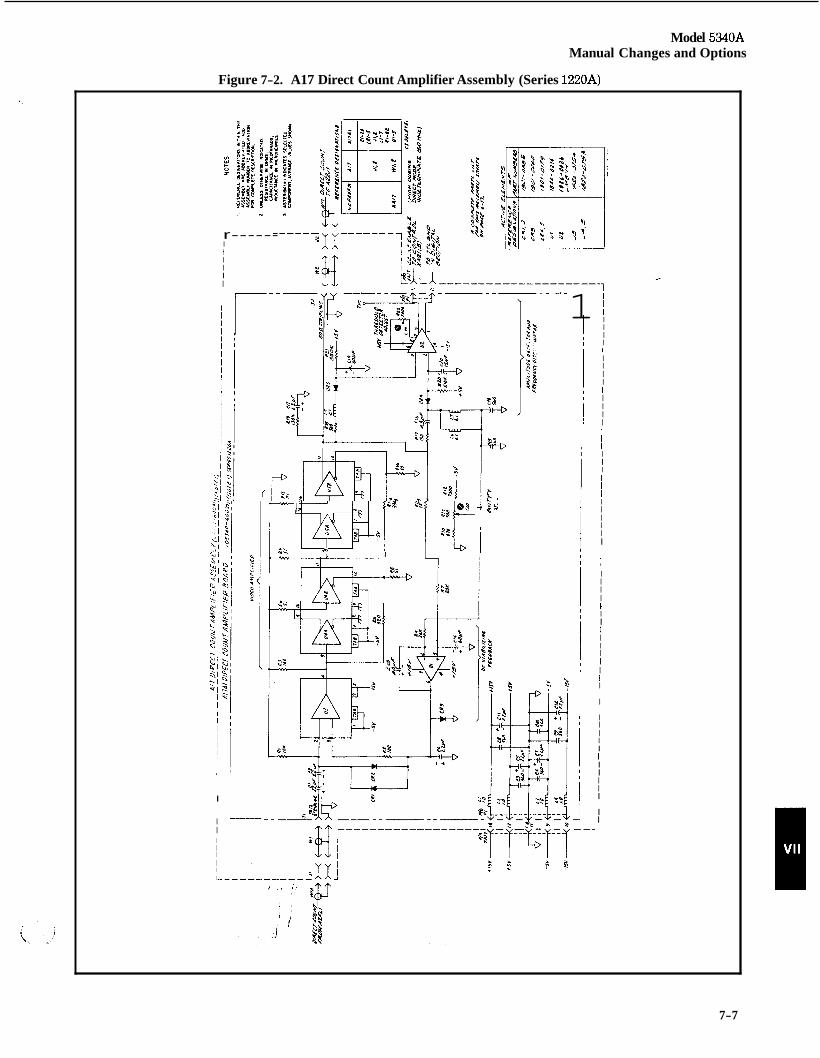
Model 5340A Manual Changes and Options
Figure 7-2. A17 Direct Count Amplifier Assembly (Series 1220A)
r------ I I I I I I r-
I I IL I I
I-
4
I: j $ 3 sb.
i
1
1 I I
I I 1 I I I I I I I I I I I I I I I I
I I I I I 1 1 I I I I I I 1 I I I I I I I. I I I I I I I I I I I I I I I I I I I I I I I I I I I
7-7
Model 534QA Manual Changes and Options
Figure 7-3. A17A1 Direct Count Amplifier Assembly (Series 1220A)
7-8
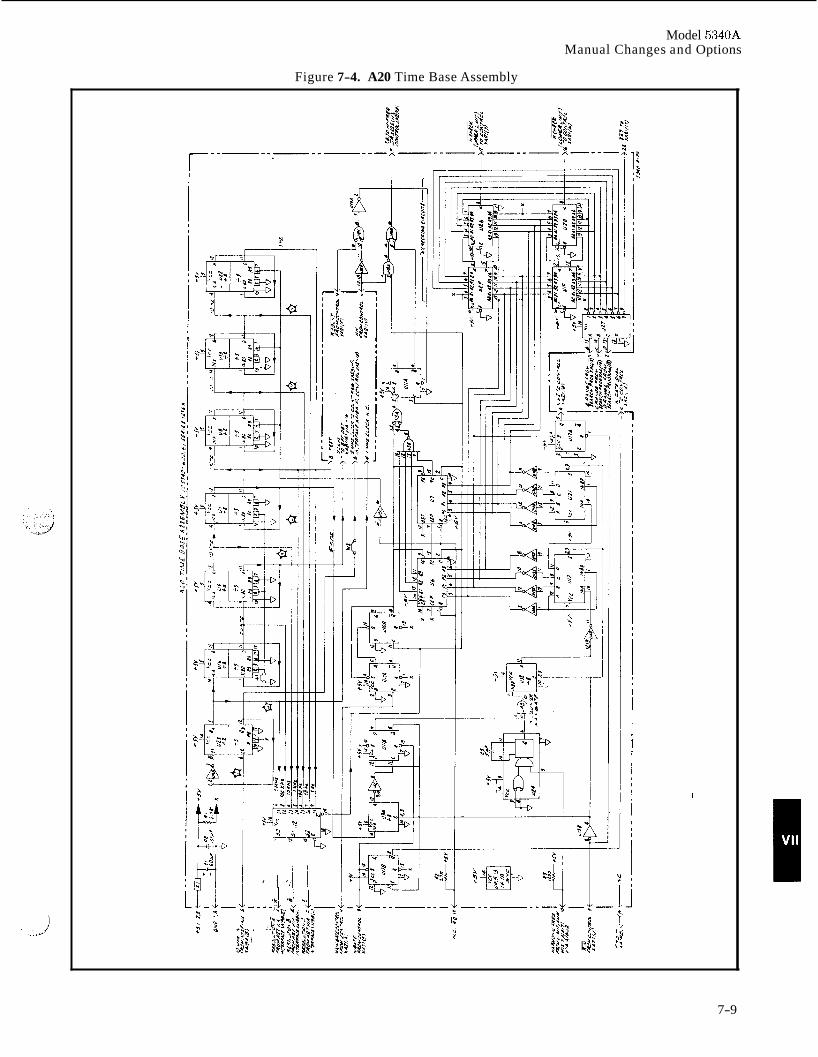
Model 5340A Manual Changes and Options
Figure 7-4. A20 Time Base Assembly
r
l'rr I < I
7-9
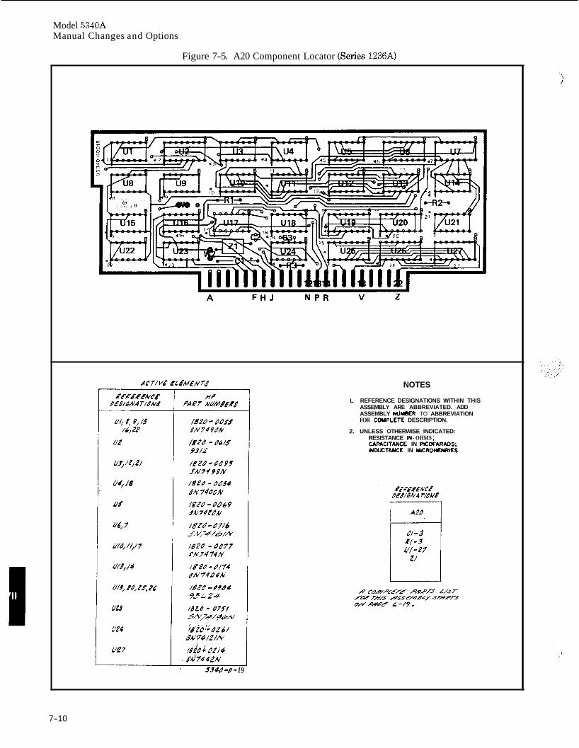
Model 5340A Manual Changes and Options
Figure 7-5. A20 Component Locator (Series 1236A)
I SS40 -R - I9
NOTES
1. REFERENCE DESIGNATIONS WITHIN THIS ASSEMBLY ARE ABBREVIATED. ADD ASSEMBLY NUMBER TO ABBREVIATION FOR COUPLETE DESCRIPTION.
2. UNLESS OTHERWISE INDICATED: RESISTANCE IN. OHMS ; CWACITANCE IN PICOFARADS; INWCTANCE IN WCROHEWIES
7-10
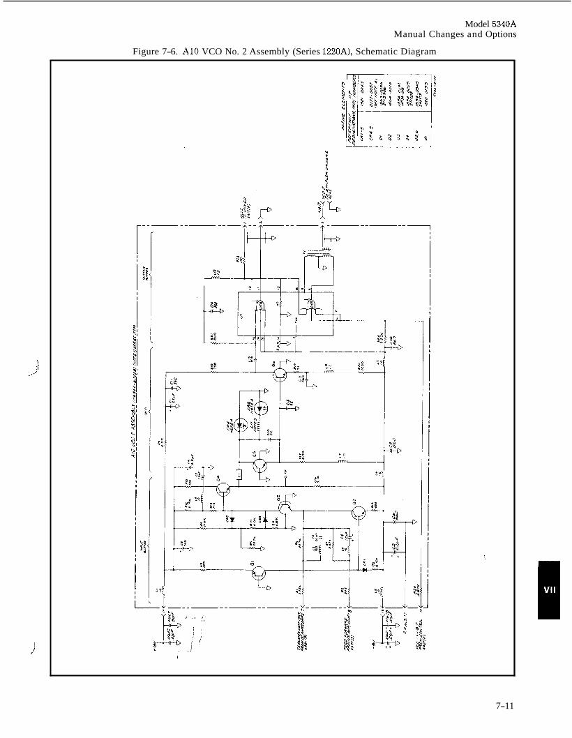
Model 5340A Manual Changes and Options
Figure 7-6. A10 VCO No. 2 Assembly (Series 1220A), Schematic Diagram
I
7-11
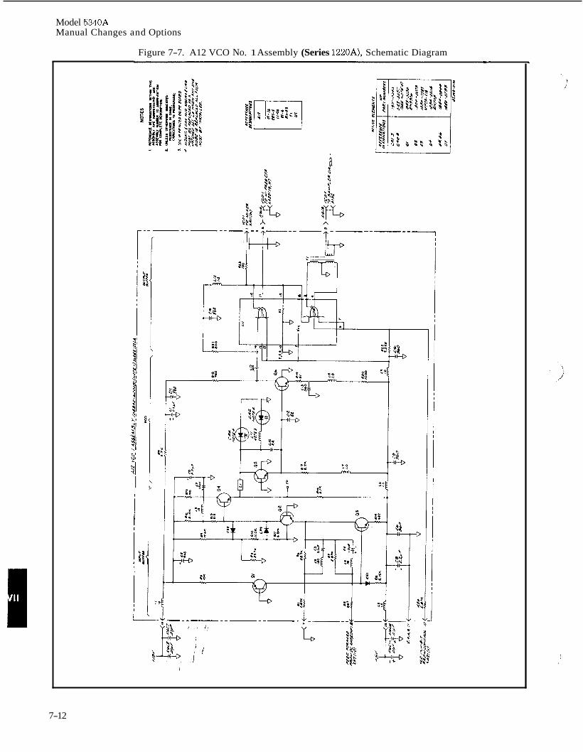
Model 5340A Manual Changes and Options
Figure 7-7. A12 VCO No. 1 Assembly (Series 1220A), Schematic Diagram
a
I ,
I I &
7-12
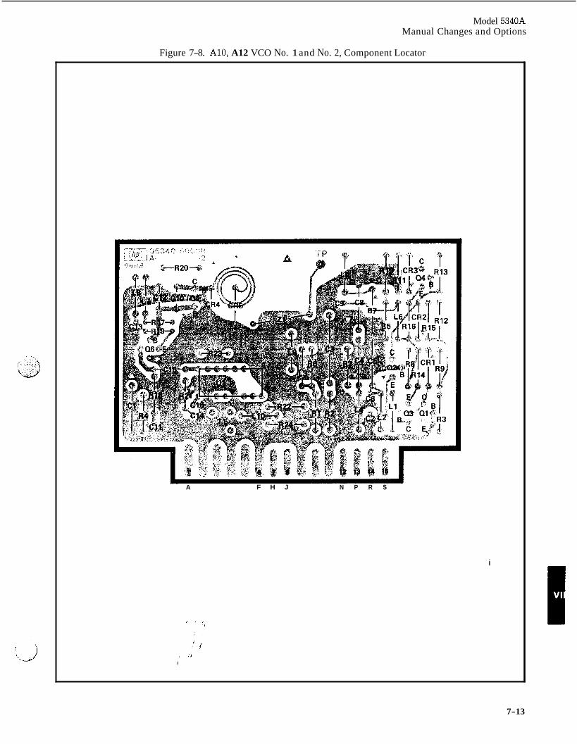
Model 5340A Manual Changes and Options
Figure 7-8. A10, A12 VCO No. 1 and No. 2, Component Locator
A F H J N P R S
i
7-13
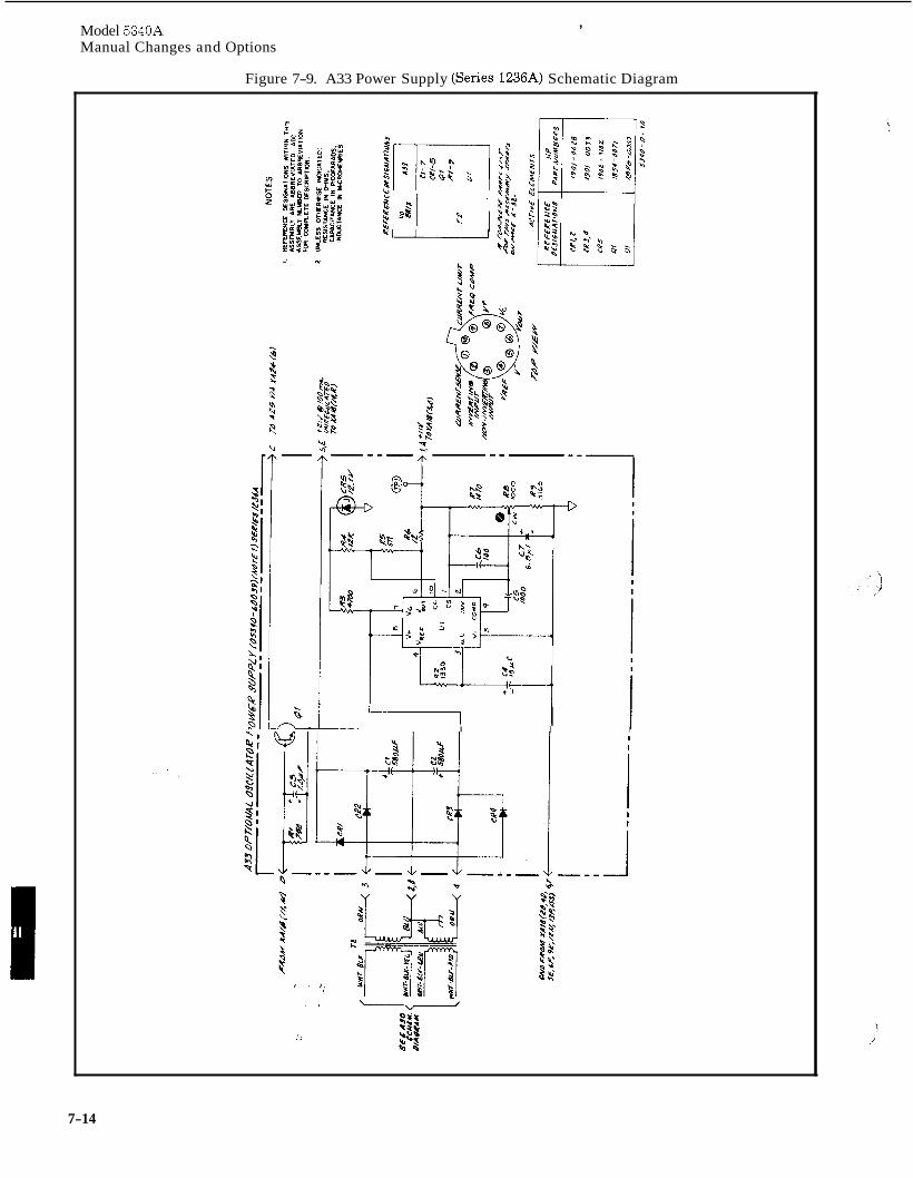
Model 5340A Manual Changes and Options
,
Figure 7-9. A33 Power Supply (Series 1236A) Schematic Diagram
.I P j > ‘1
7 I
:I
I I I
7-14
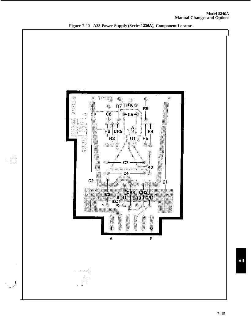
Model 5340A Manual Changes and Options
Figure 7-10. A33 Power Supply (Series 1236A), Component Locator
I
A F
7-15
Model 5340A Manual Changes and Options
7-9. OPTIONS
7-10. Options 001, 002, and 011 are available for the 5340A. Following is a description of each option.
7-11. Option 001 High-Stability Oscillator
7-12. Specifications for Option 001 are listed in Table 1-3. This option consists of deleting the standard oscillator assembly (05340-60036) and adding the following assemblies and parts:
a. A18 10544A oscillator assembly plugs into XA18 in place of the standard oscillator. The
b. A33 Power Supply (plugs into XA33). The schematic diagram is shown in Figure 8-35
c. Transformer T2. The schematic diagram is shown in Figures 8-33 through 8-35. The
schematic diagram is.shown in Figure 8-24. The parts list is given in Table 6-3.
and the parts list is given in Table 6-3. Theory is contained in Section IV.
part number is listed in Table 6-3.
7-13. Option 002, Rear Panel Connectors
7-14. This option provides input connectors on the rear panel. Input 1 (10 Hz - 18 Hz Type N 52) is installed on the rear panel in place of J1 on the front panel. Input 2 (10 Hz - 250 MHz BNC 58) is installed on the rear panel in addition to 54 on the front panel. In addition, a 50-ohm termination is installed on the front panel BNC connector 54. The termination reduces the input impedance to 50-ohms. This ensures that the 5340A meets all specifications when Option 002 is installed. When the 5340A is equipped with this option, 10 Hz to 250 MHz direct count inputs can be connected to either the rear panel (58) or the front panel connector (54). When the input is connected to the front panel input, the termination is removed and installed on the rear panel BNC connector J8. Parts for Option 002 are listed in Table 6-4. See Figures 8-2, 8-4, and 8-5 for connector locations. The schematic diagram for the direct count input is shown in Figure 8-9. The wiring for the rear panel N connector is the same as the front panel configuration, see Fig- ure 8-6.
7-15. Option 011, Remote Programming and Digital Output
7-16. Option 011 provides for remote programming and digital output. The digital output feature requires additional accessory equipment to interface with HP printers, computers, and calculators (see Table 1-2). Also, see Table 1-3 for specifications.
7-17. Option 011 consists of deleting assembly A19A and adding the parts listed in Table 6-5. Schematic diagrams are given in Figure 8-26 and 8-36. > the assemblies associatedwith th i s option is given in Section IV 7-18. Operation and programming information is given in Section 11. T eory of Operation for i. 7-19. FIELD INSTALLATION OF OPTIONS
7-20. Installation of Option 001, High-Stability Oscillator
7-21. The following parts are required:
A18 5061 - 6cSj A33 05340- 60080,
2420-OOOf 05340-2Oq44
T2 9100-~0 9'
2360701 7
3050-0066
Qecillator Assembly Oscillator Power Supply Transformer 6-32 Snap Hex Nut Oscillator Spacer 6-32 x 5/16 Pan Head Screw with lock washers Washer:Flat #6
1 ea. 1 ea. 1 ea. 2 ea. 2 ea. 2 ea.
2 ea.
7-16
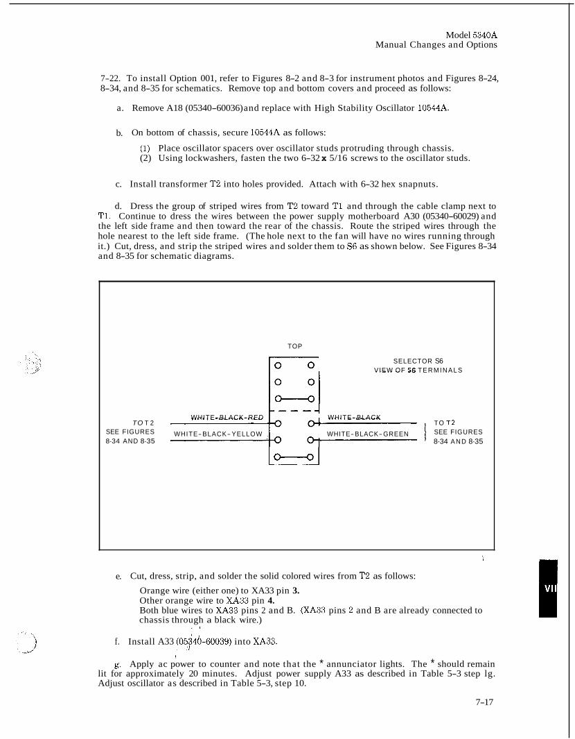
Model 5340A Manual Changes and Options
7-22. To install Option 001, refer to Figures 8-2 and 8-3 for instrument photos and Figures 8-24, 8-34, and 8-35 for schematics. Remove top and bottom covers and proceed as follows:
a. Remove A18 (05340-60036) and replace with High Stability Oscillator 10544A.
b. On bottom of chassis, secure 10544A as follows:
(1) Place oscillator spacers over oscillator studs protruding through chassis. (2) Using lockwashers, fasten the two 6-32 x 5/16 screws to the oscillator studs.
c. Install transformer T2 into holes provided. Attach with 6-32 hex snapnuts.
d. Dress the group of striped wires from T2 toward T1 and through the cable clamp next to T1. Continue to dress the wires between the power supply motherboard A30 (05340-60029) and the left side frame and then toward the rear of the chassis. Route the striped wires through the hole nearest to the left side frame. (The hole next to the fan will have no wires running through it.) Cut, dress, and strip the striped wires and solder them to S6 as shown below. See Figures 8-34 and 8-35 for schematic diagrams.
TO T 2 SEE FIGURES 8-34 AND 8-35
TOP
SELECTOR S6 VIEW OF S6 T E R M I N A L S
WHITE-BLACK T O T 2 SEE FIGURES I 8-34 A N D 8-35
WHITE-BLACK-RED
WHITE-BLACK-YELLOW , WHITE-BLACK-GREEN
e. Cut, dress, strip, and solder the solid colored wires from T2 as follows:
Orange wire (either one) to XA33 pin 3. Other orange wire to XA33 pin 4. Both blue wires to XA33 pins 2 and B. (XA33 pins 2 and B are already connected to chassis through a black wire.)
' 1
f. Install A33 (05446-60039) into XA33.
g. Apply ac power to counter and note that the * annunciator lights. The * should remain lit for approximately 20 minutes. Adjust power supply A33 as described in Table 5-3 step lg. Adjust oscillator as described in Table 5-3, step 10.
I
7-17
Model 5340A Manual Changes and Options
7-23. Installation of Option 002, Rear Panel Connectors
7-24. The following parts are required:
R4 11593A 50-ohm termination 1 ea. W17 05260-6034 Low Frequency Input Cable 1 ea. W18 05340-60060 18 GHz Rigid Coax Assembly 1 ea. 58 1250-0102 BNC connector 1 ea.
For 58 08731-201 Nut 1 ea. MP18 05340-00024 Front Panel Trim (not necessary for field
modification. Has no cutout for 51. May be installed if desired to have field modification match factory installed option).
7-25. To install Option 002, refer to Figures 6-1, 8-4, and 8-5 for instrument photos and proceed as follows:
a.
b.
Remove right trim plate MP1, right side cover MP13, and right side frame MP12.
Remove left trim plate MP1 and remove the two screws that fasten the front panel (MP15) to the left side frame (MP3).
c. Remove nut that secures the front panel to the chassis (MP4).
d. On CP1, loosen the coupling nut that secures the rigid coax line to 51.
e. Loosen 51 and push it rearward out of the front panel. Save the nut that secures the N connector to the front panel. This will be used for the rear panel N connector. Also save the aligning pin from the front panel N connector.
,j f. On rear panel, remove plugs in holes for 52 and 58. If original front trim panel is retained,
insert plug into hole left after removal of 51.
g. Install N connector of assembly 05340-60060 into rear panel hole marked 52. Dress rigid coax along the right side of chassis and through the two cable clamps. Use the nut from the front panel N connector and the aligning pin to oreint and secure 52 to the rear panel. Do not overtighten the nut on 52.
DO NOT TIGHTEN THE FITTINGS ON CP1 TO MORE THAN 12 IN-LBS. DAMAGE TO FITTINGS MAY RESULT.
h. Secure the rigid coax cable fitting to CP1.
i. Secure cable W17 (05260-6034) to BNC connector (1251-0102). Push cable end through hole marked 58 on the rear panel. Use nut (08731-201) to secure connector. Roate low frequency cable from rear panel along the right side of chassis through the two cable clamps.
j. If desired to replace front panel trim (MP17), remove knobs and hardware for S1, S2, R1/S3, and S4. Also unsolder the capacitor lead that connects from A3 to 54. Remove 54 from front panel. Install new trim panel MP18.
' 1'
k. Solder the center conductor of the low frequency cable to the center pin of 54. Solder the \
i shield to the ground pds$ next to 54.
J 1.
m.
Reassembly' the front panel, side frames, and side covers.
Install 50-ohm termination on 54.
7-18
Model 5340A Manual Changes and Options
7-26. Installation of Option 011, Digital Input/Output
7-27. The following parts are required:
A19
A34
A35
w19, w20
A20
CR2
05340-60032
05340-60067
05340-60068
8120-0520
05340-60073
1901-0028
05340-00026
2360-0197
2200-0103
2190-001 7
Interface B Assembly 1 ea.
Bus Communicator Assembly 1 ea.
Connector Assembly 1 ea.
ASCII Bus Cable 2 ea.
Time Base Assembly (Required for instruments with serial prefix 1252A and below. The 05340-60018 board must be replaced with an 05340-60073 board.
Diode 1 ea.
Insulator 1 ea.
Pozi-drive Screws 6-32 x 3/8 4 ea.
Pozi-drive Screws 4-40 x 1/4 4 ea.
Lockwashers for Standoff 2 ea. Stud Mount
Solder Lug 1 ea.
7-28. and 8-36. To install Option 011, proceed as follows:
Figure references that are useful during installation include Figures 8-2, 8-3, 8-5, 8-26,
a. Remove A19A (05340-60031).
b. On the rear panel, remove the blank plate by removing the four pozi-drive screws.
c. On A19B (05340-60032) install cables W19 and W20 in sockets J1 and 52 located on the right edge of the board. See Figure 8-26 component locator. Pins 1 and 14 of both cable con- nectors should be oriented toward the top of the pc board. The white arrows on the connector will point toward the board. W19 will be the cable connected to the top most socket of A19B.
I d. Install A19B into XA19 and dress the cables past the casting assembly toward the reariof
the instrument.
e.
f.
Install 05340-60073 Time Base board into XA20 for instruments not so equipped.
Locate A34 (05340-60067). Connect the plug from cable W19 to the socket on A34 that is closest to integrated cirauit U3. Connect the d u g from cable W20 to the socket adjacent to the
I - I
large 24-pin Cinch connector. The white arrows on the connector will point toward the board.
g. Install A34 beh,@ 2 the rear panel. Align the four standoffs on A34 toward the rear panel. The 24-pin Cinch ccmnector on A34 should be aligned toward the bottom of the instrument. Use four 6-32 x 3/8" pozi-drive screws to secure A34 to the rear panel. Dress cables W19 and W20 along the casting assembly and away from the power supply boards. Install the insulator between the power supply boards and W19 and W20.
7-19
Model 5340A Manual Changes and Options
h. Install A35A1 (05340-60066) and A35J1 (Digital Input-Output Type 57 connector) in the Option 011 plate (plate with the six slide switches). See Figure 8-5 for correct orientation of A35J1. Secure A35J1 using the standoff stud mount and split lock washers. Using four 4 x 40 x I/”
posi-drive screws, secure the Option 011 plate to the outside rear panel. The pc insterconnect board mates with A34J1. Except for the black wire, route the wires soldered to the slide switches to- ward the bottom of the chassis.
i. Locate the black wire soldered to switch A35S6 (TALK-ALWAYS). Solder the other end of the black wire to the black wire already soldered to switch S5 (INT-EXT).
j. Prepare a #22 or #24 gauge insulated wire (WHT-BLK-RED) approximately 30” long. Solder one end to XA24 (05340-60019) pin 4. A diode (HP part number 1901-0028) should be installed between XA24 pin 4 and pin 2 (see Figure 8-36). Connect cathode (marked end) to pin 4.
k. Route the 30” wire along the front edge of the chassis past A1 on to the top of the chassis. Continue to route the wire along the right top of the chassis rearward toward the rear panel. Route the wire to the bottom of A34 and solder to the A34 eyelet marked +5 V on Figure 8-36 component locator.
1. Solder the violet wire from A35S6 (TALK ALWAYS-ADDRESSABLE) to the A34 eyelet marked S6 on Figure 8-36.
m. Solder the blue wire from A35S6 to the A34 eyelet marked “Shield” on Figure 8-36.
n. Solder the green wire from A35S5 (switch A5) to the A34 eyelet marked S5 on Figure 8-36.
0. Solder the yellow wire from A35S4 (switch A4) to the A34 eyelet marked S4 on Figure 8-36.
p. Solder the orange wire from A35S3 (switch A3) to the A34 eyelet marked S3 on Fig- ure 8-36.
q. Solder the red wire from A35S2 (switch A2) to the A34 eyelet marked S2 on Figure 8-36.
r. ure 8-36.
s. This completes installation of Option 011 refer to Paragraph 7-15 for descriptions. See
Solder the brown wire from A35S1 (switch Al) to the A34 eyelet marked S1 on Fig-
Section I1 for programming information.
7-20
Model 5340A Schematic Diagrams
SECTION Vlll
SCHEMATIC DIAGRAMS
8-1. SCHEMATIC DIAGRAMS
8-2. This section contains schematic diagrams, assembly and chassis part locators, component locators, block diagrams, waveforms, test points, and troubleshooting information. The sche- matics are presented in assembly number order A1 through A35 The component, chassis, and assembly locators show the location by reference designator. The block diagrams give a simplified block of the corresponding schematic diagram. Test points, waveforms, and typical voltages are given as an aid in troubleshooting.
8-3. SCHEMATIC DIAGRAM NOTES, ASSEMBLY NUMBERS, AND REFERENCE DESIGNATORS
8-4. Figure 8-1 shows the symbols used on the schematic diagrams. At the bottom of Figure 8-1, the system for reference designators, assemblies, and subassemblies are shown.
8-5. Reference Designations
8-6. Assemblies such as printed circuit boards are assigned numbers in sequence, Al , A2, etc. As shown in Figure 8-1, subassemblies within a n assembly are given a subordinate A number. For example, rectifier subassembly A1 has the complete designator of A25A1. For individual components, the complete designator is determined by adding the assembly number and sub- assembly number if any. For example CR1 on the rectifier assembly is designated A25AlCR1.
8-7. Identification Markings on Printed-Circuit Boards
8-8. HP printed circuit boards (see Figure 8-1) have four identifications numbers; an assembly part number; a series number, a revision letter, and a production code.
8-9. The assembly part number has 10 digits (such as 05340-60037) and is the primary identifi- cation. When a production change is made on an assembly that makes it incompatible with previous assemblies, a change in part number is required. The series number (such as 1248A) is used to document minor electrical changes. As changes are made, the series number is incremented. When replacement boards are ordered, you may receive a replacement with a different series number. If there is a difference between the series number marked on the board and the schematic in this manual, a minor electrical difference exists. If the number on the printed-circuit board is lower than that on the schematic, refer to Section VII for back dating information. If it is higher, refer to the loose leaf manual change sheets for this manual. If the manual change sheets are missing, contact your local Hewlett-Packard Sales and Service Office. See the listing on the back cover
All assemblies with the same part number are interchangeable.
of this manual. I
8-10. Revision letters (A, B, etc.) denote changes in printed circuit layout. For example, if a capacitor type is changed (electrical value may remain the same) and requires different spacing for its leads, the printed circuit board layout is changed and the revision letter is incremented to the next letter. When a revision letter changes, the series number is also usually changed. The production code is'the'four digit, seven segment number used for production purposes.
' / 8-11. ASSEMBLY LOkATIONS AND COMPONENT LOCATORS
8-12. Figures 8-2 through 8-5 show the front, rear, top, and bottom views of the 5340A. Following these is an overall block diagram and schematic diagrams for the instrument. Component locators for each printed circuit assembly are located next to the schematics.
8-1
Model 5340A Schematic Diagrams
8-13. MNEMONICS AND ABBREVIATIONS
8-14. Table 8-1 lists mnemonics and abbreviations peculiar to the 5340A. Common ab- breviations are given in Section VI.
Table 8-1. 5340A Mnemonics and Abbreviations
CHK CLK CONT CTR DAC DAV DIO DIR CNT DIR SW DISP REG D.P. IFC F.F. Fx HI-Z I.L. INH INT M. GATE ATN N.C. O'FLO PE P/O PROG P SHIFT P TRAN Q R COUNT R DISP REMT REN RES A RES B RFD R.N. s=7 SEL S RATE S RATE Q SRQ S TRAN S TRAN QUAL SUB SWA S W B TB T.L. T P ' I !
VCD + 5 J DG
.i
Check Clock Control Counter Data Accepted Data Valid Data Input Output Direct Count Direct Switch Display Register Decimal Point Interface Clear Feed Forward Input Frequency High Impedance Input Loop Inhibit Internal Main Gate Attention No Connection Overflow Parallel Enable Part of Program Parallel Shift Parallel Transfer Qualifier Reset Counter Reset Display Remote Remote Enable Resolution A Resolution B Ready For Data Reset N Counter Search in Seventh Step Select Sample Rate Sample Rate Qualifier Service Request Serial Transfer Serial Transfer Qualifier Subtract Switch A Switch B Time Base Transfer Loop Test Point Voltage Controlled Oscillator t5V Power For Digital Circuits
8-2
Model 5340A Schematic Diagrams
Figure 8-1. Schematic Diagram Notes
SYMBOLS
F R O N T P A N E L
REAR P A N E L
INTERIOR A N D P C BOARDS
WIPER MOVES TOWARD “CW” WHEN CONTROL I S R O T A T E D CLOCKWISE
POWER L I N E GROUND
C IRCUIT COMMON GROUND
F L O A T I N G GROUND
CHASSIS GROUND
KNOB CONTROL
SCREWDRIVER ADJUST
REVISION LE lTER
7-SEGM ENT PRODUCTION CODE
MAIN S IGNAL P A T H
F E E D B A C K P A T H
T E S T POINT
“AND” G A T E
“OR” G A T E
I N V E R T E R
N A N D G A T E
NOR G A T E
E X C L U S I V E NOR
PRlNTED CIRCUIT BOARD IDENTI FCATION
HP PART NO.
MANUFACTURING CODE
SERIES NO. (May Be Stamped Elsewhere On The Board)
REFERENCE DESIGN AT1 0 N S
R E F E R E N C E DESIGNATIONS WITHIN ASSEMBLIES ARE A B B R E V I A T E D . ADD ASSEMBLY NUMBER T O A B B R E V I A T I O N FOR C O M P L E T E DESCRIPTION. JACKS A R E THE M O V E A B L E OF TWO CONNECTORS.
S T A T I O N A R Y CONNECTORS AND PLUGS A R E THE MORE
ASSEMBLY ABBREVIATON COMPLETE DESCRIPTION A25 c1 425C1
C R I A25A1 CR1 A25A1 NO P R E F I X J 3 J 3
A-cembly S t 1 N o Asgembly Sene5 No f i n r l u d e s A 2 5 A l ( u s r d 10 document A < x r n b l y As\embly
Number Name A ~ ~ e m b l y l change?)
A W r - - - - * A25 POWER SUPPLY AsSY(05100-6007) SERIES 1220A --
J 3 not mounted 12 mounrtd on A i i c m b l v A 2 5 A r s r m b l y
N u m h c r a indi idtc I Part ol A 2 5
lrom J3 to Pin 6 01 PI on
A ~ r e m b l y A5 T e r m r i d I Number, I I Pin Numbers I
8-3
Model 5340A Schematic Diagrams
Figure 8-2. 534012 Top Internal View (with Options 001, 002, and 011 Installed)
R4
I , i ,
8-4
Model 5340A Schematic Diagrams
52
A19J1
A19J2
A35J1
Figure 8-3. 5340A Bottom Internal View and Cable Numbers and Connections (with Options 001, 002, and 011 Installed)
CP1
A34Pl
A34P2
External Equipment
Figure 8-3. 5340A Bottom Internal View and Cable Numbers and Connections (with Options 001,002, and 011 Installed)
Cable No.
w1
W2
w 3
w4
w 5
W6
w7
W8
w 9
w 10
w11
w12
W13
W14
W15
W16
W17
W18
w19
W20
w21
Cable Name
AC Line Switch
18 GHz Input
Sampler #1
A3 Output
Sampler #2
A1 Output
VCO 1/AIA2
AC Line Cord
A2 output
A2FLl Input
Direct Count output
10 MHz Douhlei
VCO 1/m
VCO 2/A2A2
Harm hq A14/A20
Main Chassis
Low Freq Inpui Option 002
18 GHz Input Option 002
ASCII Bus
ASCII Bus
Remote Prog Digital output
Conned8
From
s1 J1
CPI
A3 Output
CPI
A l J l
A I M 1
J 6
A U 1
A17J1
A17J2
A19A(E)
A16J6
MAW1
A16J2
TO
s6
CP1
A1J2
XA2X21)
A U 2
A16J4
A16J5
115/23OVAC
A16J3
A2FLlJ4
A2U1
Al6J1
A2q19)
A16J7
A2W10)
Primary Interconnect
J 8 I 54
HP Part Number
05505-6C019
05340-60028
0534o-Mx)33
05340-60034
05340-60013
0534o-60035
0534o-60044
8120-1378
05340MK)48
05340-6c049
05340MMm
05340-60051
05340-60052
05340-60053
05340-60054
0534060065
05260-6034
0534060060
05340-60063
05340-60063
8120-1833
Wiring Method
~~
Soldered
Connectors
Connectars
Soldered
Connectom
Connectors
Connectors
Connectors
Connectors
Connectors
Connectors
19 End-Solderc 416 - Connecta
.22 End-Soldm 416 - Conneeto
Connectom
20 End-Solden 416 - Connecto
-
Soldered
Connectors
connectars
Connectam
Connector
a 5
. . . . . . . . . . . . . . . . . . . . . . . . . . . . . . . . . . . . . . . . . . . . . . . . xaow L ~ v d* +
LNI o ~ v
. . . . . . . . . . . . . . . . . . . . . . . . . . . . . . . . . . . . . alU8lOd l83!VaA 33BIlOS 3NhS 3 a O W d 3 3 M S
......................................... . . . . . . . . . . . . . . . . . . . . . . . . . . . . . . . . . .
:oI SloJluOl adoasoiiino W S
' p s n SWM a q o q .'apv!a I:OI ' a w a u u EOZBI PUS =y! iduv P ! l r a h VIWI qllm ada3soipso VOBI [ a p W d H qlW U a W @ q8nOlql @ SWOPAWM
i 'map OZ- 18 rndu! ZHW OZE qilm u a q q S W O f a A E M @ 103 i d a x 3
- A 0
- A 0
A 0
L
Model 5340A Schematic Diagrams
A25DS 12 A25DS9 A25DS1 thru A25DS8 A250S10
~ 2 5 % ? ~ \ \ / / l A 2 5 D S l l A
si si A i l J4 S4 J l
A35S5 A35S3 A35S1 TH 1
Figure 8-5. 5340A Rear Panel Reference Designations (with Options 002 and 011 Installed) i
F'1 S6 J3 A36J1 A55 Mb7 B1 J2 (PART OF
, , , A35A1)
'I 8-7
8-8
. . . . ................... . . . . . ........... . . I , ,* ~ >:,n"; XE j: , ,.: . , ..-
A1A4 1 r---------- A1 A1 A1 A 3
1 20MHz I*TO A13
I
I
AMPLIFIER
FILTER SAMPLER
F x F R O M ~ CP1 #1 OUTPUT
SAMPLER - ~~~~~ SAMPLER 1 A12 D R I V E R
A 1 A 4
I AMPLIFIER AMPLIFIER I r---------- 1 I I
FILTER I I 20MHz 1,
I )TO A 1 3
I
r----------
I I I I I I
I I Pf I
Tw7
NOTES
2. UNLESS OTHERWISE INDICATED: RESISTANCE IN OHMS; CAPACITANCE IN PICOFARADS; INDUCTANCE IN MICROHENRIES
3. ASTERISK I*) INDICATES SELECTED COMPONENT. AVERAGE VAWES SHOW
A i PREAMPL/F/€R ASSEMBLY NO./ l ' 05340 -6OOf7 )
REF€RENC€ DEESfGNATfONf
A/ 1 AIAl I AIAZ I AIA3 I AIA4 I Cf -24
LI-9
Qi, 2 RI-31
U I
PI, P
I f5Y
ACT/& €C€M€NfJ
81, 2
U f
I
-/5Y
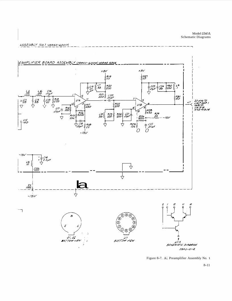
Model 5340A Schematic Diagrams
L4
4
- --i"-- / o m 4
. -
I . /5Y
--
la
0 0
I
I ' I I
-- I I I
I I I I I
I I I I I I I
3
1
Figure 8-7. A1 Preamplifier Assembly No. 1
8-11
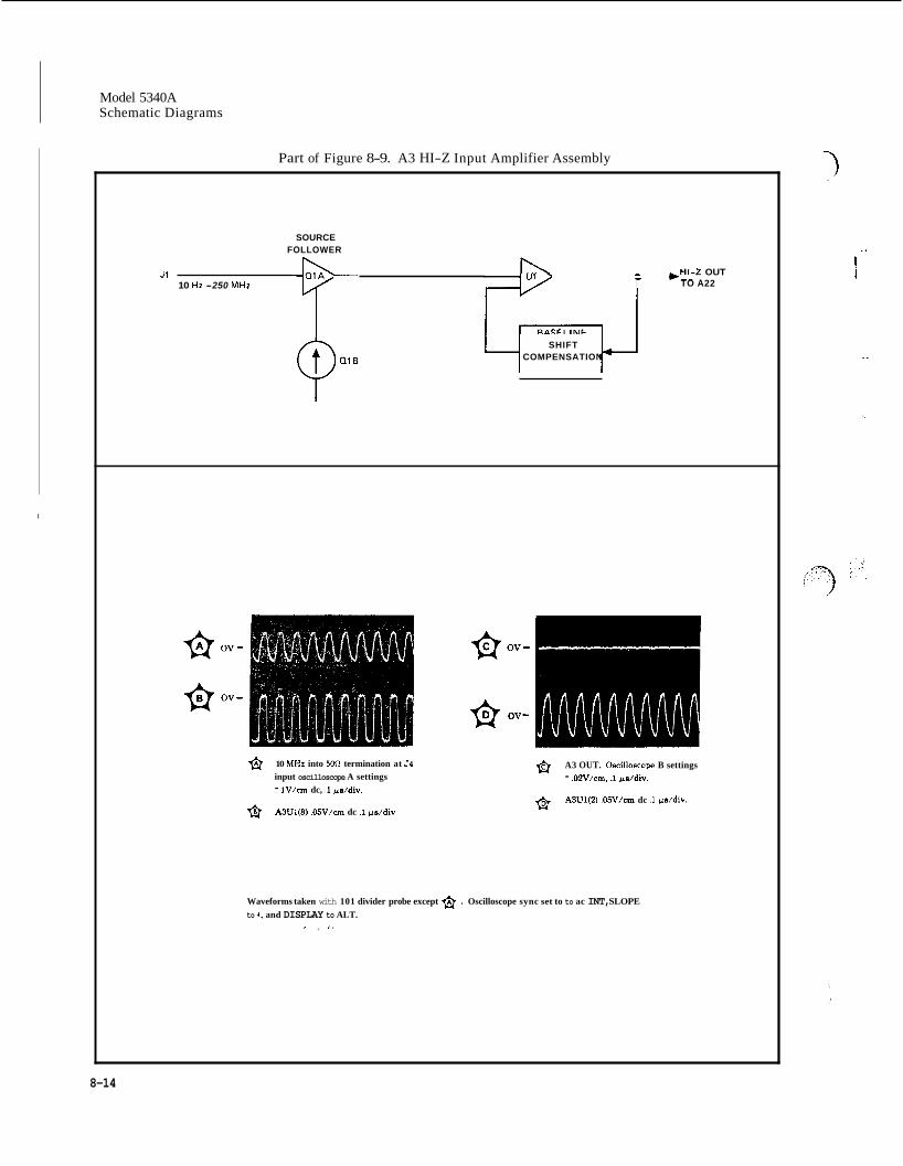
Model 5340A Schematic Diagrams
I
Part of Figure 8-9. A3 HI-Z Input Amplifier Assembly
SOURCE FOLLOWER
) H I 4 OUT TO A22
- J1 10 Hz -250 MHz
SHIFT COMPENSATION
& 10 MHz into 5oR termination at 54 input oscilloscope A settings - lV/cm dc, .1 pddiv.
A3U1(8) .05V/cm dc .I ps/div &
& A3 OUT. Oscilloscope B settings - .OQV/cm. .I ,u/div.
A3U1(2) .05V/m dc .1 p/d iv . &
Waveforms taken with 101 divider probe except & . Oscilloscope sync set to to ac INT, SLOPE to +, and DISPLAY to ALT.
I , ,,
..
8-14
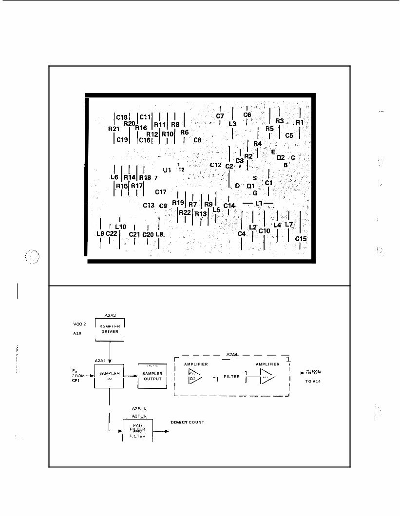
D R I V E R A 1 0
A2A4 A2A3 1 ----_----- - I AMPLIF IER AMPLIF IER I
I 2 0 M H z
T O A14 I I I
F I L T E R +*NFo SAMPLER I OUTPUT CPI
I I
ARF.Ll,,
47b FILTER
T O D I R E C T A 1 7 C O U N T
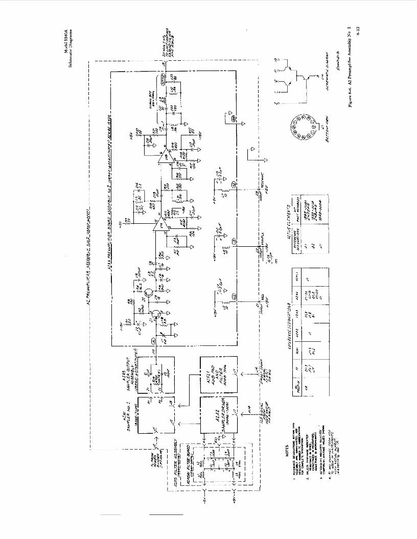
L
I
I I
_ _ I I
I
I I 1 I I I I I I I I
$ 1 t
I
, , i ,
1 j
I 6
Igl,
14“ -iL
I I
1: , $
I I I I I I I I I
A
20MH7 REF FROM- A15
F H J
t Q 4 . 0 5
20 MHz I F F R O M A 1 3
D I FFE RENT1 A L AMPL l F IER
Q U A 0
PHASE OETl OUT TO A 6
I Q U A D
A M P L l F IER
QUAD D E T )OUT TO A5
I
SHIFT I
Pg
R\---- r
1.
I h
1
I
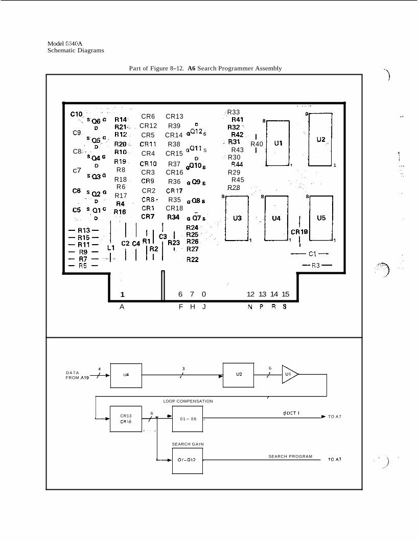
Model 5340A Schematic Diagrams
r
1
Part of Figure 8-12. A6 Search Programmer Assembly
L
6 7 0 12 13 14 15
4
- 3 I
I F D A T A FROM A19- u4
R33
R31 R40 R43 I
R30 R44 1
R29 R45
R28
6 I
I u2
-
I
I LOOP COMPENSATION
6 ~ D E T 1 - F TO A 7 CR13
c1- -R3-
-
- CR18
I
0 1- 0 6 . - * , I
c9
C8 s Q 4 G R19
R8 c7 sQ3G R18
-- R6
D
SEARCH G A I N
SEARCH PROGRAM TO A7 _+ Q7-012
R17 cu S w G
CR6 CR13 CR12 R39 CR5 CR14 a 012,
C R l l R38 CR4 CR15 CRIO R37 &los CR3 CR16 CR9 R36 ~ Q 9 s CR2 C R l 7
CRI CR18
aQ11 S
D
CR8. R35 G Q 8 s
- R 5 -
A F H J N P R S
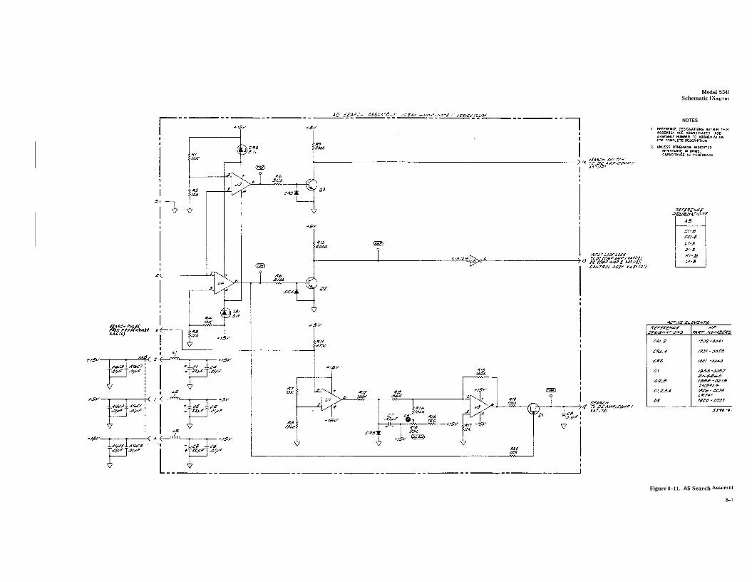
Model 534( Schematic Diagrar
/z a
NOTES
C I - 8 CR/-5 11-3 01-5 RI-ld JI-5 -
Figure 8-11. A5 Search Assembl
8-1
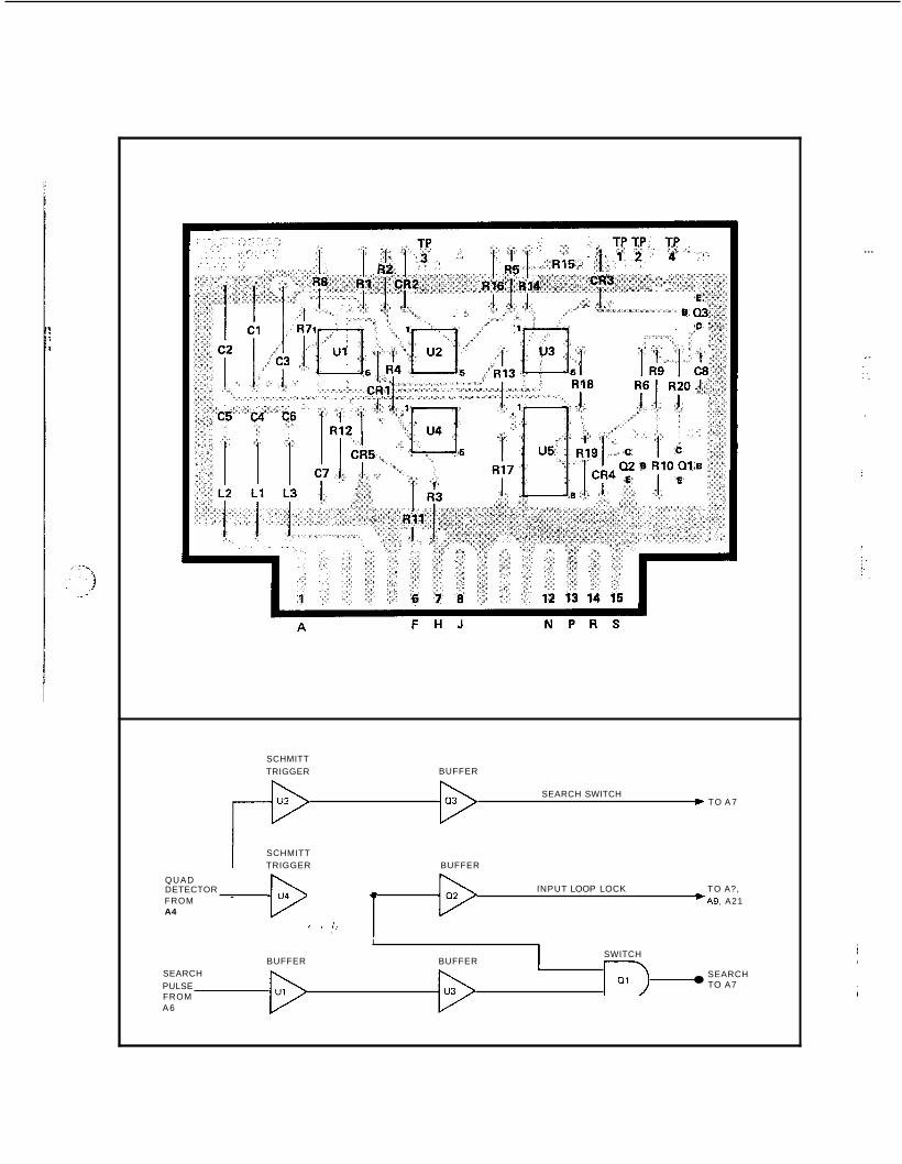
SCHMITT TRIGGER BUFFER
SEARCH SWITCH b TO A 7
SCHMITT I TRIGGER BUFFER
- INPUT LOOP LOCK TO A?, )A9. A21
QUAD DETECTOR FROM A4
-
I
1 SWITCH BUFFER BUFFER
SEARCH TO A7
SEARCH PULSE FROM A 6
...
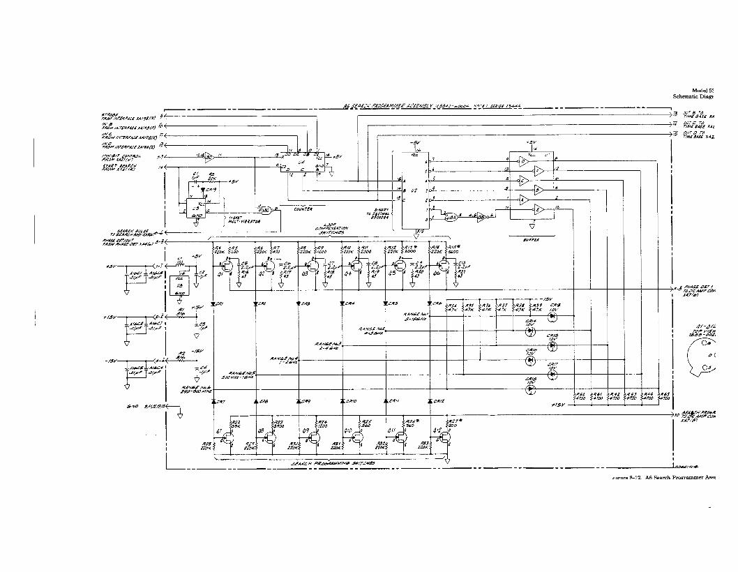
I
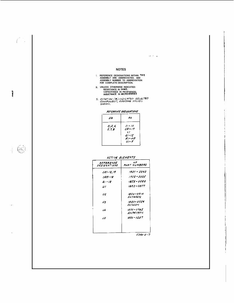
1 , ,
NOTES
I . REFERENCE DESIGNATIONS WITHIN THIS ASSEMBLY ARE ABBREVIATED. ADD ASSEMBLY NUMBER TO ABBREVIATION FOR COMPLETE DESCRIPTION.
2. UNLESS OTHERWISE INDICATED: RESISTANCE IN OHMS; CAPACITANCE IN PICOFARADS; INDUCTANCE IN MICROHENRIES
I I
5-344 -D -7
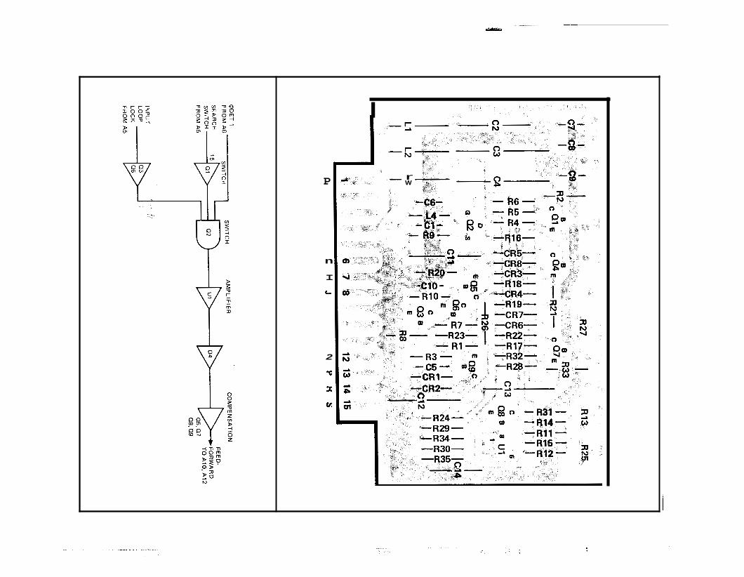
P
n
I
c
2
w
X
v!
I
r W
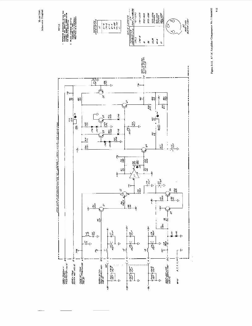
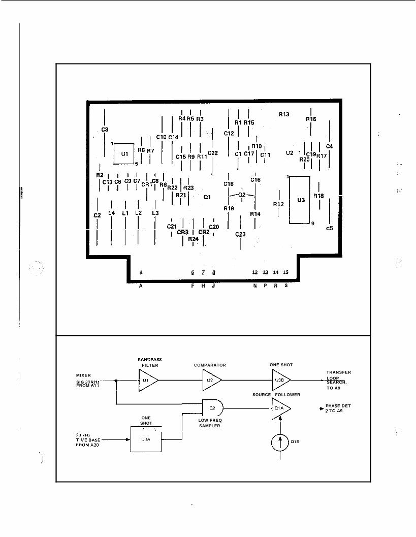
I
1 6 7 8 12 13 14 15
A F H J N P R S
I I
R12
1
1 I
R18
9 c5
C23
BANDPASS FILTER COMPARATOR ONE SHOT
TRANSFER - LOOP MIXER
SIG 20 kHz SEARCH, FROM A1 1
- T O A9
r
SOURCE FOLLOWER
PHASE DET ) 2 T O A 9
LOW FREQ SAMPLER
ONE SHOT
I I / /
s
m
1
I
Q 4- 0
%
R1
I
FROM A8
I I +
1 I
R 8
R3
T O A10
I I 1
c1 L2
SEmm' FROM A8
INPUT LOOP LOCK FROM A5
c3 L1
COMPARATOR FOLLOWER
- ONE SHOT BUFFER - r d
U6A r
E
I I 1
A F H J N P R S
AMPLIFIER
I I 1 ,
T R A N S F E R LOOP LOCK TO A21

M I
I I I
>ils VZP
S310N
A J s
TRANSFER LOOP FREQ CONTROL CONTROLLER OSC BUFFER FROM A 1 9 - FEED- )TO A l l FORWARD FROM A7
vco 2
, ,
99* .D I
S3J.ON
I 1 0 7 97
A F H J N P R S
M I X E R
vco 2 FROM A10-I
20 kHz )MIXER
OUT TO A8
, U2
vco 1 't' FROM A12
..
I
L ? a ea
+t-D
FREQ FEED CONTROLLER OSC BUFFER FORWARD FROM A7 - vco 1
TO ~ i i
9 Q 3 I , ,
i
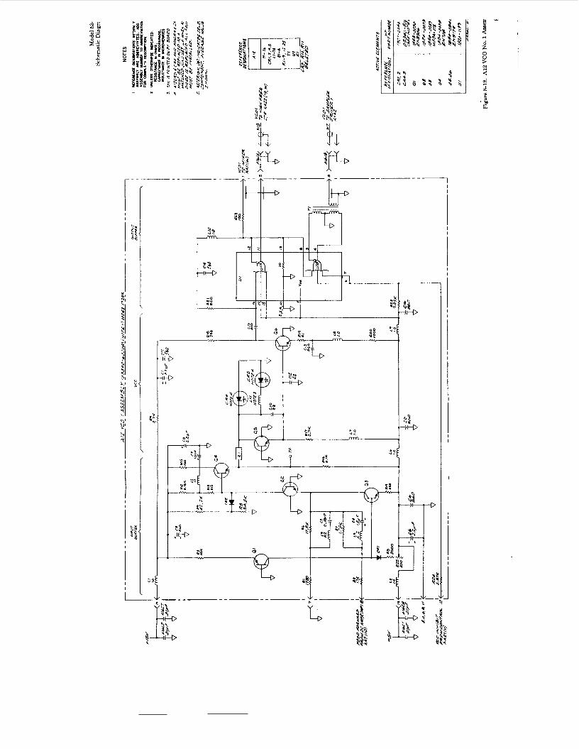
6 ' II
I
I
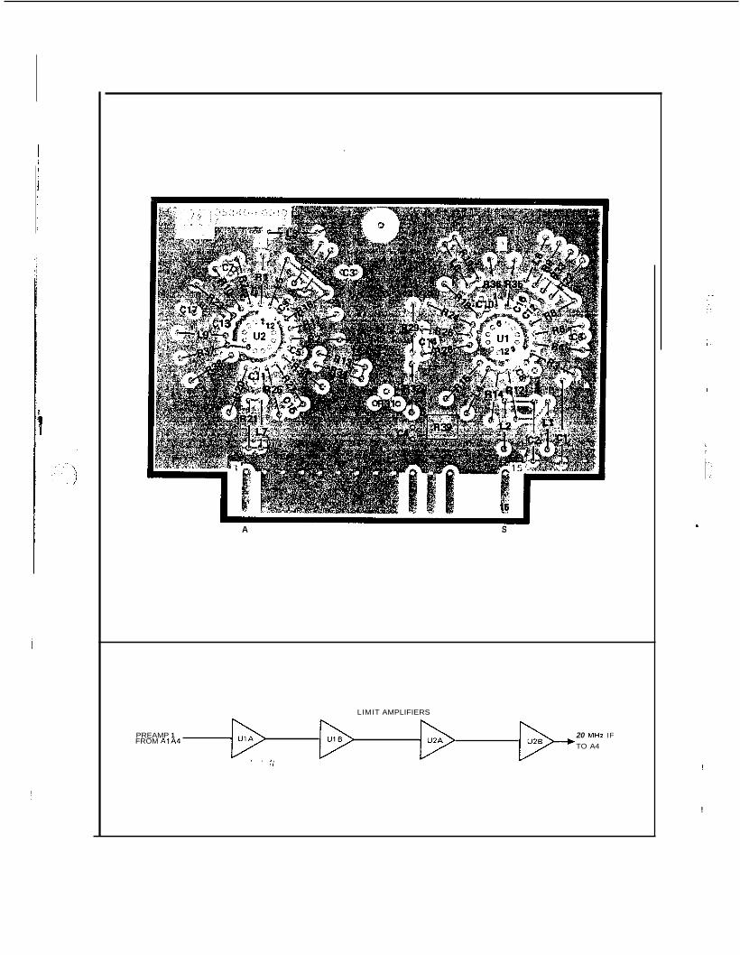
A S
LIMIT AMPLIFIERS
PREAMP 1 20 MHz IF FROM A1A4
TO A4
' ' :/
I
!
!
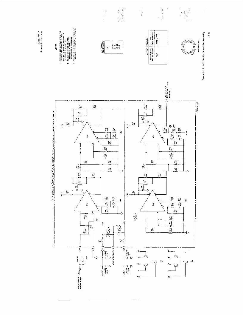
.
.
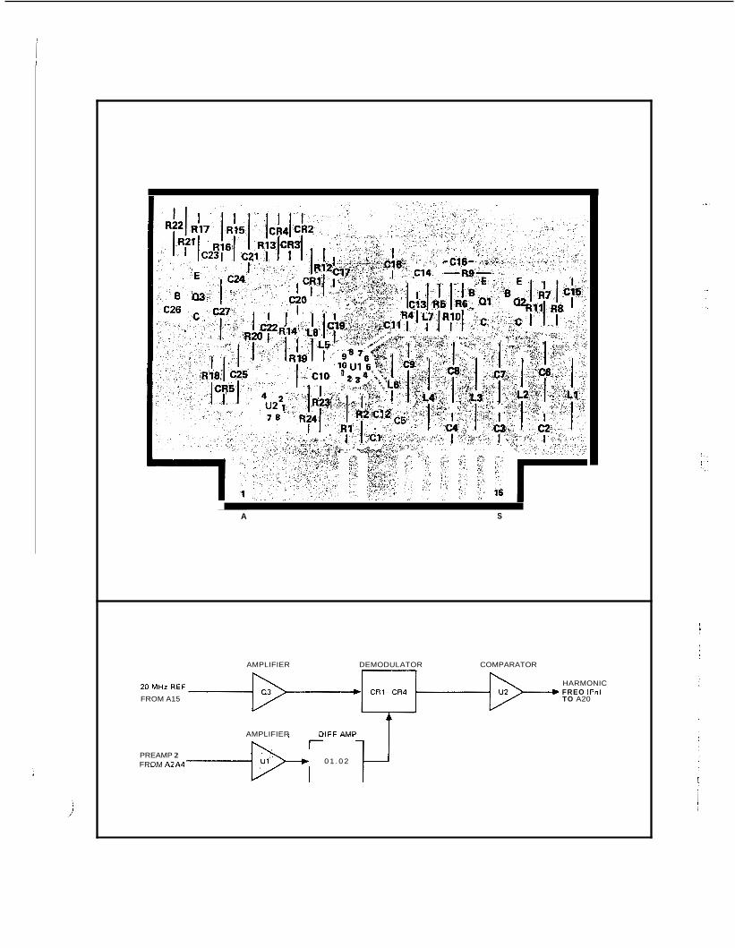
A S
AMPLIFIER DEMODULATOR COMPARATOR
HARMONIC FREO ( F n l
FROM A15 TO A20
AMPLIFIER DlFF AMP
0 1 . 0 2 PREAMP 2 FROM A2A4
i
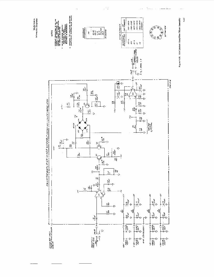
I I
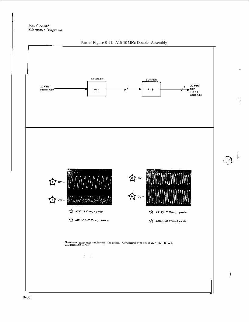
Part of Figure 8-21. A15 10 MHz Doubler Assembly
10 MHz FROM A19 b
DOUBLER
2 0 M H z
TO A4 AND A14
I U l A b U1B I ,REF , 2 I
BUFFER -
Waveforms taken with oscilloscope 1O:l probes. Oscilloscope sync set to INT, SIX)PE. to t, and DISPLAY to ALT.
I ,
8-38
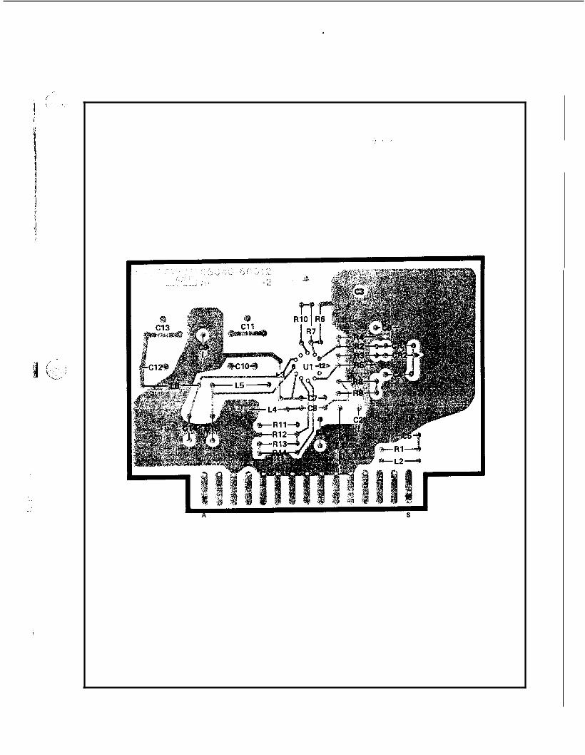
A S
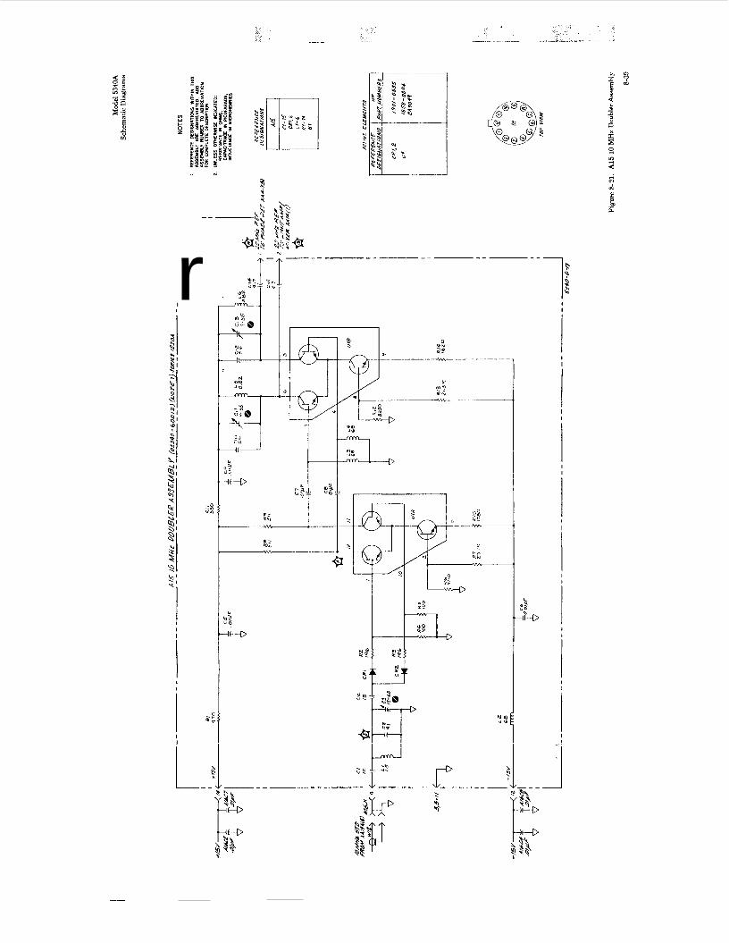
r --___
I
I
Model 5340A Schematic Diagrams
A16 CASTING MOTHERBOARD ASSEMBLY 05340-60015
A16 is a six layer interconnect board used to interconnect assemblies A4 through A15 and also to provide connections to other points in the counter. The symbol denotes a feedthrough point. For example, the inhibit signal connects to XA10(10), XAll(lO), and XA12(10). The signal is used by A10 and A12. The connection a t XAll(10) is for convenience only and is not used by A l l .
Since multilayer construction is used for A16, extreme care should be used when unsoldering wires, connectors, and jacks. Use the minimum amount of heat necessary to unsolder parts. When replacing the printed-circuit connectors, clip off the connector from the top of the board, then unsolder each pin.
Care should be taken when connecting cables to J1 through 57. Use a straight on motion for mating the connectors.
Figure 8-22. A16 Casting Motherboard
'-I-/ 1 I I'
8-41
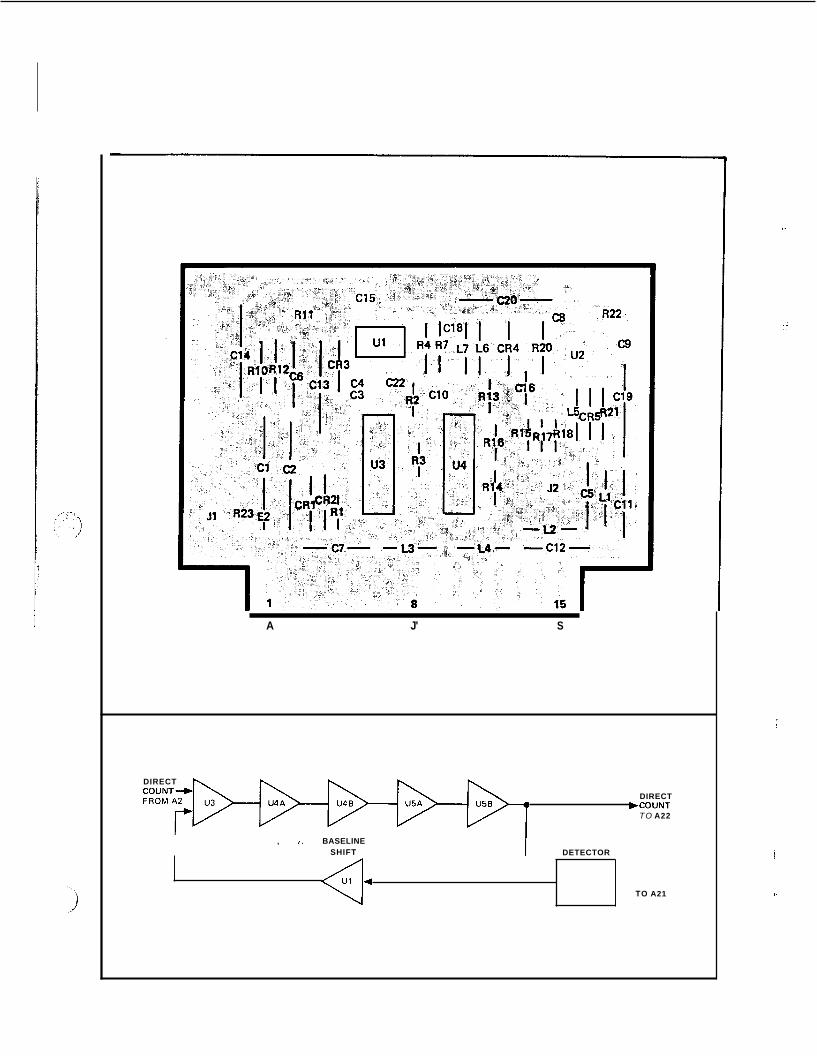
A J' S
TO A21
DIRECT COUNT-+
DIRECT )COUNT
TO A22
, ,, BASELINE SHIFT I DETECTOR
I . .
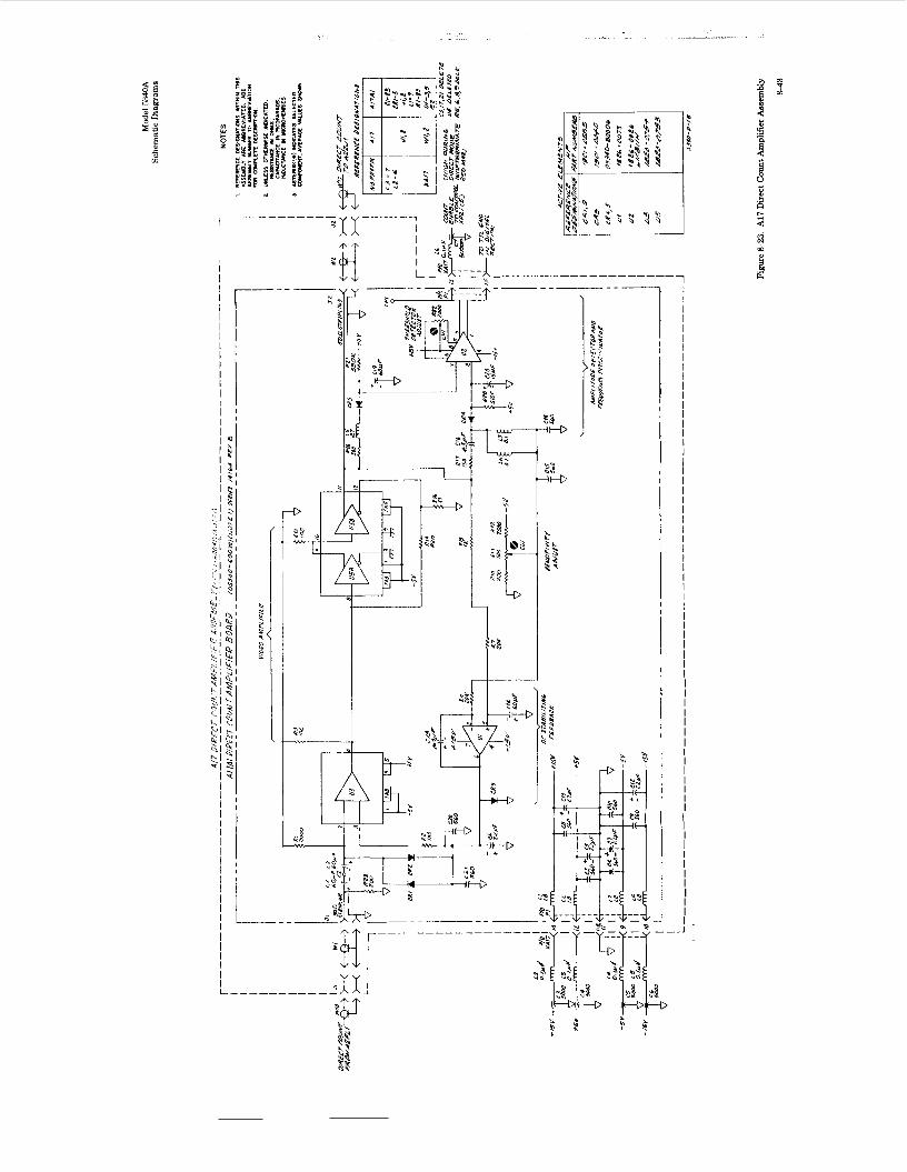
- w n
r----------
2 I..
I I I I I I I I I I I I I I I I I I I 1 I I I I I
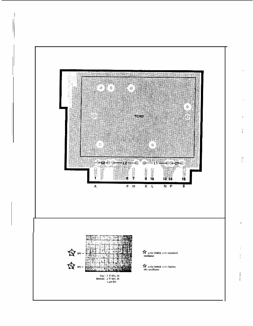
A F H K L N P S
ov
ov
b is for 5340A with standard oscillator
& is for 6340A with Option 001 oscillator
Top: .1 V/div, dc Bottom: .1 V/div, dc
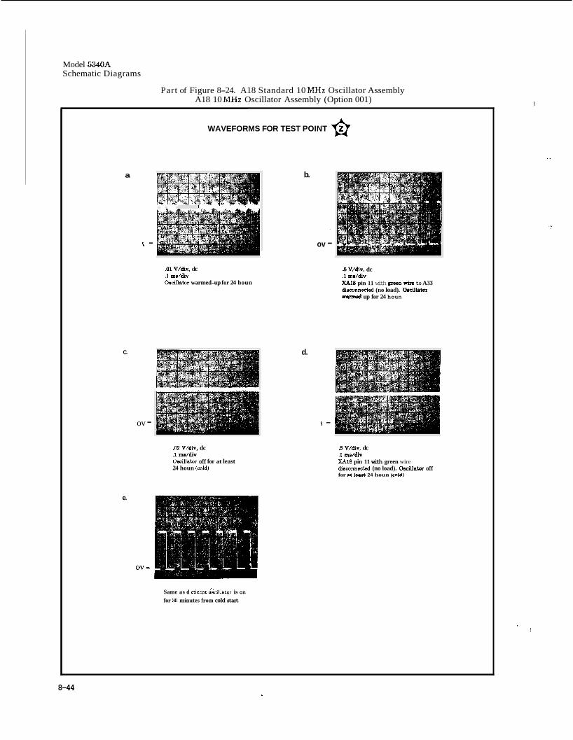
Model 5340A Schematic Diagrams
Part of Figure 8-24. A18 Standard 10 MHz Oscillator Assembly A18 10 MHz Oscillator Assembly (Option 001)
WAVEFORMS FOR TEST POINT &
a
C.
I
ov -
.01 V/div. dc
.1 ms/div O d a t o r warmed-up for 24 houn
ov -
.02 V/div. dc
.1 ms/div Omcillator off for at least 24 houn (mld)
e.
Same as d e&ept &illator is on for 30 minutes from cold start
b.
ov -
.5 V/div. dc
.1 mddiv XA18 pin 11 with gnen wire to A33 diaconnected (no load). Oneillator warmed up for 24 houn
d.
ov -
.6 V/div. dc
.l ms/div XA18 pin 11 with green wire diaconnected (no load). Oncillator off for at least 24 houn (cold)
8-44
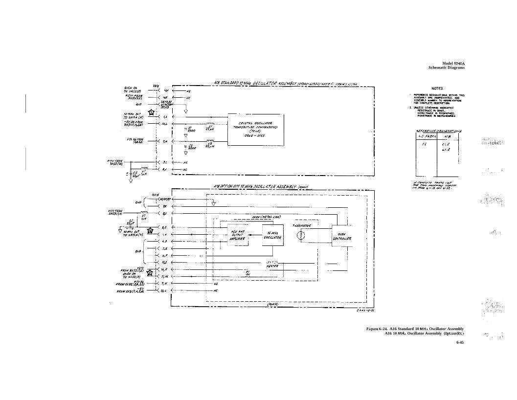
Model 5340A Schematic Diagrams
I I
!
I I I I 1 I I I I 1 I I I I ~
I I
I I
Figure 6-24. A16 Standard 10 MHz Oscillator Assembly A16 10 MHz Oscillator Assembly (Option 001)
6-45
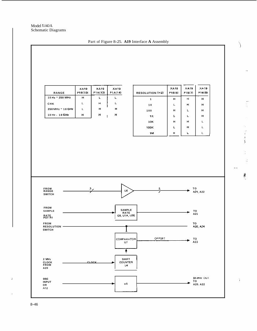
Model 5340A Schematic Diagrams
FROM SAMPLE
RATE 01, U l A . U2E POT R 1
SAMPLE RATE
J
TO A21
Part of Figure 8-25. A19 Interface A Assembly
b
osc INPUT OR u 5
RANGE
10 MHz OUT TO A20. A22
1 0 H z - 250 M H z
C H K
250 M H z - 1 8 G H z
1 0 Hz ~ 1 8 G H z
X A 1 9 P l B ( 1 0 )
H
L
L
H
H H
H H
RESOLUTION (HZ)
1
1 0
1 0 0
1 K
1 OK
l O O K
1 M
X A 1 9
P l B ( 6 )
H
L
H
L
H
L
H -
- X A 1 9
P l B ( 7 )
X A 1 9
P l B ( 8 )
H
H
H
H
L
L
L
-
2, T O / / A21, A22
FROM 3, RANGE SWITCH
FROM TO RESOLUTION A20,A24 SWITCH I
2 MHz SHIFT CLOCK CLOCK bl C0UbJ;ER 1 FROM A20
._-
8-46
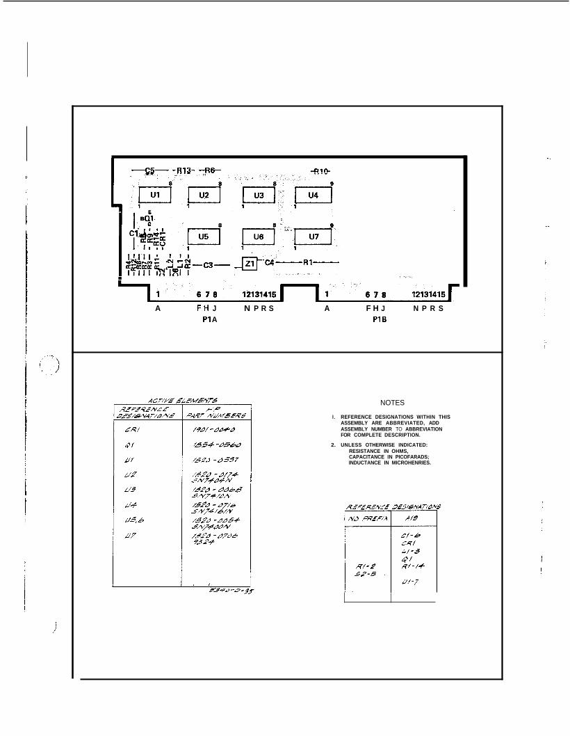
-5- -R13- - - R e
A F H J N P R S A F H J N P R S P1 A P1 B
NOTES
I. REFERENCE DESIGNATIONS WITHIN THIS ASSEMBLY ARE ABBREVIATED, ADD ASSEMBLY NUMBER TO ABBREVIATION FOR COMPLETE DESCRIPTION.
2. UNLESS OTHERWISE INDICATED: RESISTANCE IN OHMS, CAPACITANCE IN PICOFARADS; INDUCTANCE IN MICROHENRIES.
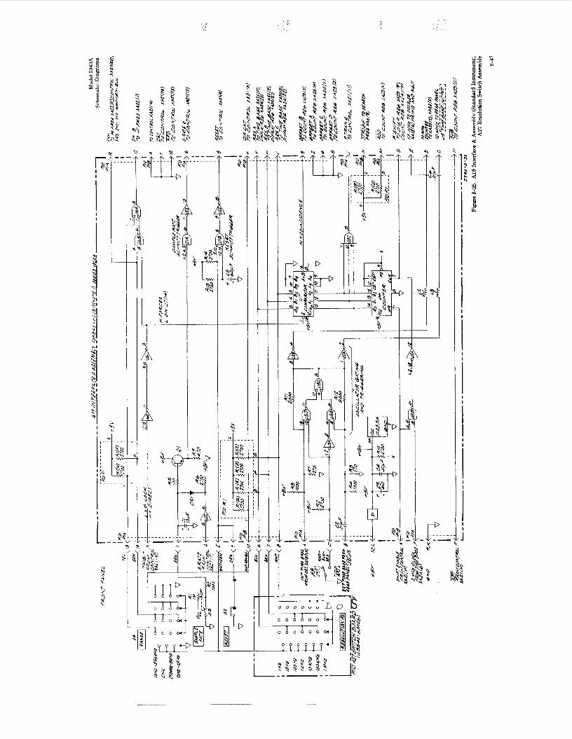
I
i
I \ I I I l“ lil
1 1 ---- 0 0 0 0 L o IS
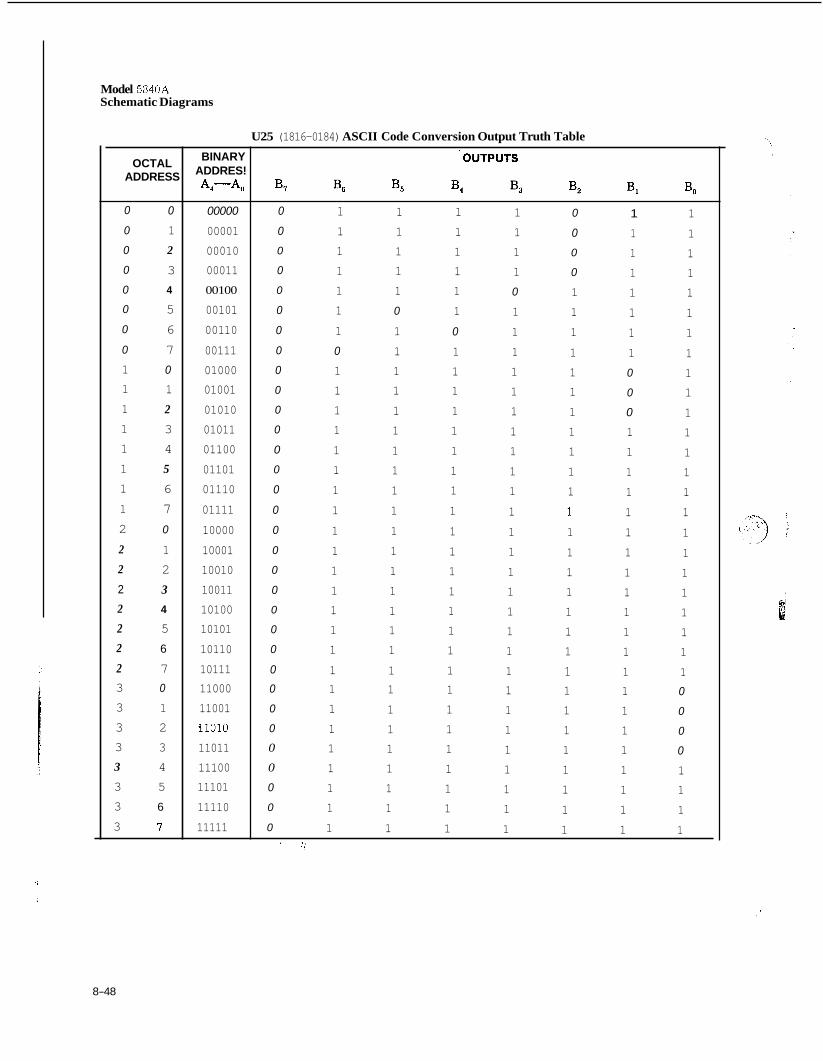
Model 5340A Schematic Diagrams
OCTAL ADDRESS
0
0
0
0
0
0
0
0
1 1 1 1 1 1 1
1 2 2
2
2
2
2 2
2 3 3 3 3 3
3 3 3
0
1 2
3 4
5 6
7 0
1 2
3 4 5
6
7 0
1 2 3 4
5 6
7 0
1 2 3 4
5
6
7
BINARY ADDRES! A,--A,
00000
00001 00010 00011 00100
00101 001 10
00111 01000 01001 01010 01011 01100 01101 01110
01111
10000 10001 10010 10011 10100 10101 10110 101 11 11000 11001 ilOl0 11011 11100 11101 11110 11111
U25 (1816-0184) ASCII Code Conversion Output Truth Table
0
0
0
0
0
0
0
0
0
0
0
0
0
0
0
0
0
0
0
0
0
0
0
0
0
0
0
0
0
0
0
0
1 1 1 1 1 1
1 0
1 1 1 1 1 1 1 1
1 1 1 1 1 1 1
1 1 1 1 1 1 1 1 1
1 1 1 1 1 0
1 1 1 1 1 1 1 1 1 1
1 1 1 1 1 1 1
1 1 1 1 1 1 1 1 1
1 1 1 1 1 1
0
1 1 1 1 1 1 1 1
1
1 1 1 1 1 1 1 1 1 1 1 1 1 1 1 1
1 1 1 1 0
1 1 1 1 1 1 1 1 1 1
1
1 1 1 1 1 1 1 1 1 1 1 1 1 1 1 1
0
0
0
0
1
1 1
1 1 1 1 1 1 1 1
1- 1
1 1 1 1 1 1
1 1 1 1 1 1 1 1 1
1
1 1 1 1 1 1 1 0
0
0
1 1 1 1 1 1 1 1 1 1 1 1 1 1 1 1 1 1 1 1 1
1 1 1 1 1 1 1
1 1 1 1 1 1 1 1 1
1
1 1 1 1 1 1 1 0
0
0
0
1 1 1 1
i
8-48
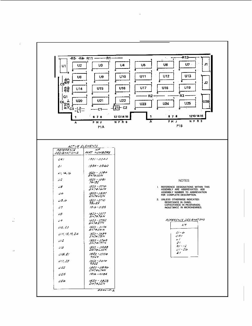
NOTES
I. REFERENCE DESIGNATIONS WITHIN THIS ASSEMBLY ARE ABBREVIATED. ADD ASSEMBLY NUMBER TO ABBREVIATION FOR COMPLETE DESCRIPTION.
2. UNLESS OTHERWISE INDICATED: RESISTANCE IN OHMS; CAPACITANCE IN PICOFARADS; INWTANCE IN MICROHENRIES.
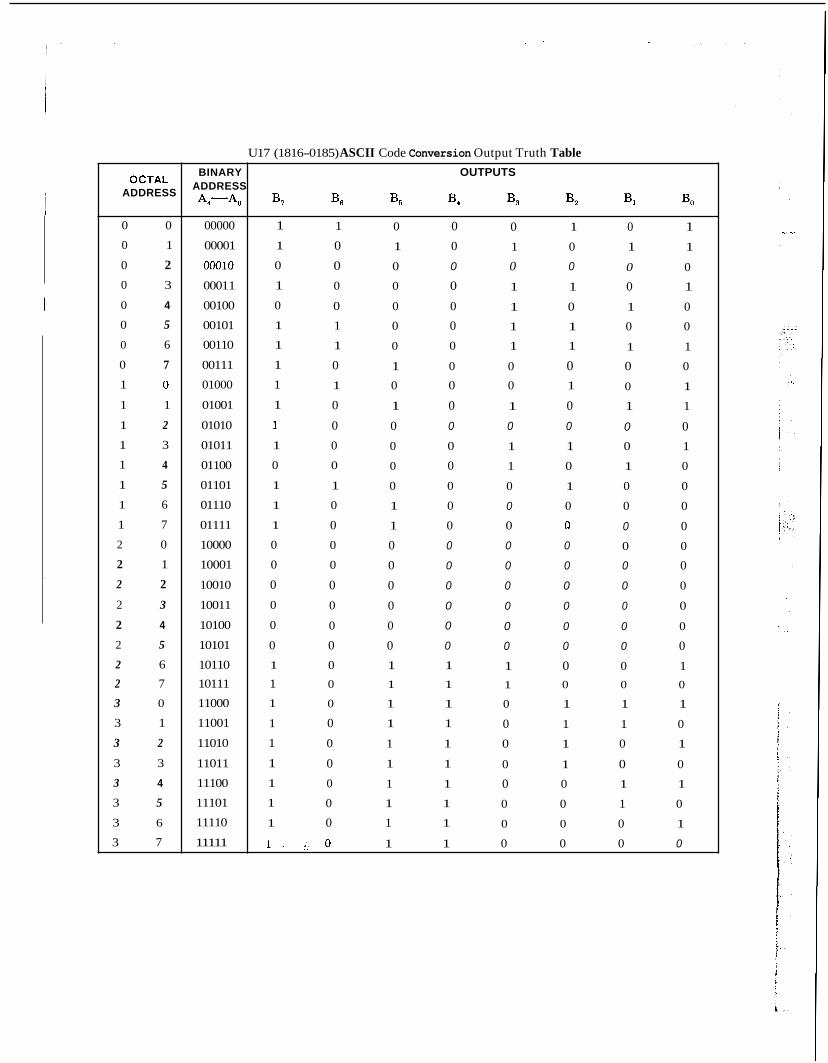
I I I
I
I
U17 (1816-0185) ASCII Code Conversion Output Truth Table BINARY OUTPUTS
OCTAL ADDRESS 4-A, B7 Bt3 B5 B* B3 B2 B, Bo
ADDRESS
0 0 00000 1 1 0 0 0 1 0 1 0 1 00001 1 0 1 0 1 0 1 1
0 2 00010 0 0 0 0 0 0 0 0 0 3 0001 1 1 0 0 0 1 1 0 1 0 4 00100 0 0 0 0 1 0 1 0 0 5 00101 1 1 0 0 1 1 0 0 0 6 00110 1 1 0 0 1 1 1 1 0 7 00111 1 0 1 0 0 0 0 0 1 0 01000 1 1 0 0 0 1 0 1
1 1 01001 1 0 1 0 1 0 1 1
1 2 01010 1 0 0 0 0 0 0 0 1 3 01011 1 0 0 0 1 1 0 1 1 4 01100 0 0 0 0 1 0 1 0 1 5 01101 1 1 0 0 0 1 0 0 1 6 01110 1 0 1 0 0 0 0 0 1 7 01111 1 0 1 0 0 0 0 0 2 0 10000 0 0 0 0 0 0 0 0 2 1 10001 0 0 0 0 0 0 0 0 2 2 10010 0 0 0 0 0 0 0 0
2 3 10011 0 0 0 0 0 0 0 0
2 4 10100 0 0 0 0 0 0 0 0 2 5 10101 0 0 0 0 0 0 0 0 2 6 10110 1 0 1 1 1 0 0 1 2 7 10111 1 0 1 1 1 0 0 0
3 0 11000 1 0 1 1 0 1 1 1
3 1 11001 1 0 1 1 0 1 1 0
3 2 11010 1 0 1 1 0 1 0 1
3 3 11011 1 0 1 1 0 1 0 0 3 4 11100 1 0 1 1 0 0 1 1
3 5 11101 1 0 1 1 0 0 1 0 3 6 11110 1 0 1 1 0 0 0 1
3 7 11111 I , , , o 1 1 0 0 0 0
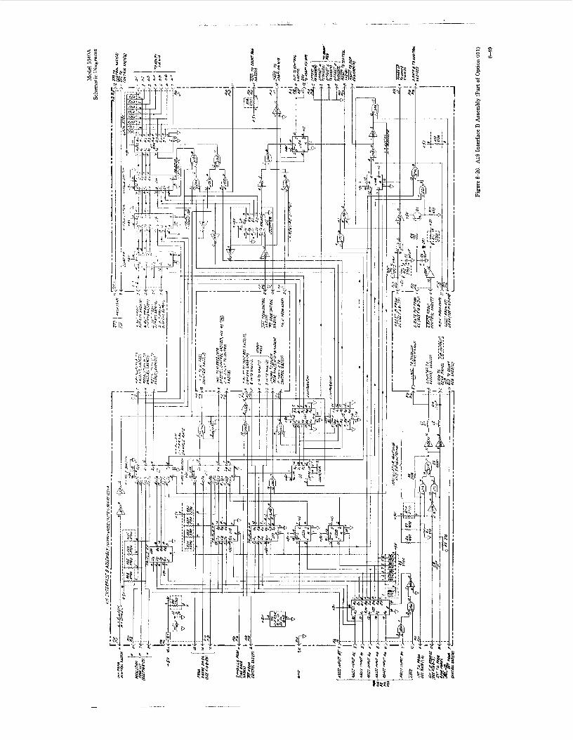
I
I
1
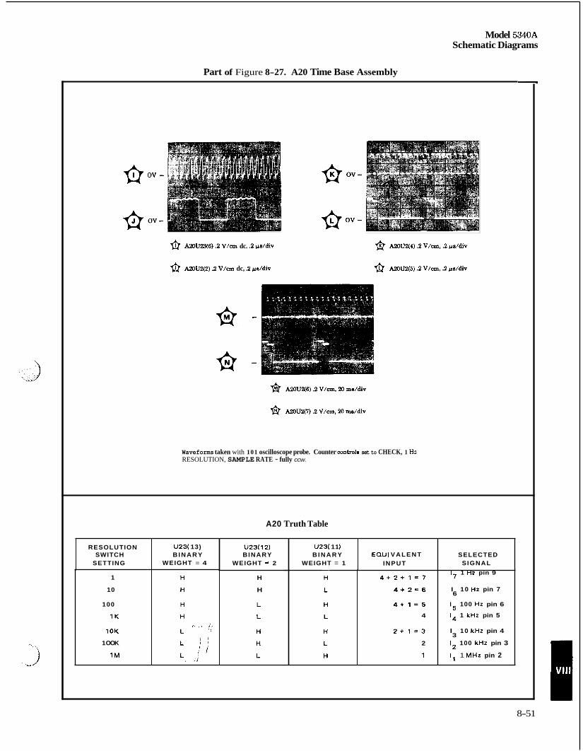
Model 5340A Schematic Diagrams
U23( 11 ) B I N A R Y
WEIGHT = 1
Part of Figure 8-27. A20 Time Base Assembly
EQUl V A L E N T INPUT
fi A2OU23(6) .2 V/cm dc. .2 rrsldiv
fi A2OUq2) .2 V/cm dc, .2 pe/div
@ m U 2 ( 4 ) .2 V/cm, .2 ps/div
fi A2OU2(5) .2 V/cm. .2 &div
Waveforms taken with 101 oscilloscope probe. Counter controls set to CHECK, 1 Hz RESOLUTION, SAMPLE RATE - fully ccw.
RESOLUTION SWITCH
SETTING
1
10
100
1K
10K
1 OOK
1 M
A20 Truth Table
U23( 13) B I N A R Y
WEIGHT = 4
U23(12) B INARY
WEIGHT - 2
H
H
4 + 2 + 1 = 7
4 + 2 = 6
4 + 1 = 5
4
2 + 1 = 3
2
1
SELECTED SIGNAL
l7 1 Hz I pin 9
I 10 Hz pin 7 6
l 5 100 H z pin 6
l 4 1 kHz pin 5
I 10 kHz pin 4 3 l2 100 kHz pin 3
I l 1 MHz pin 2
8-51
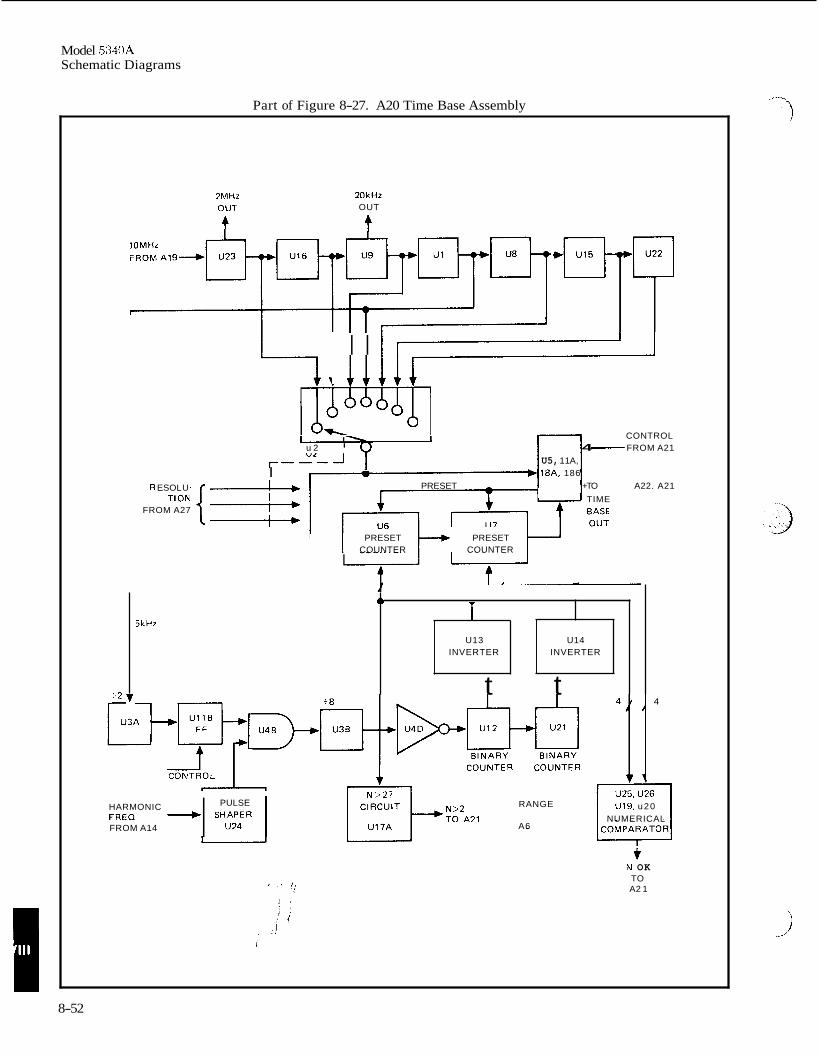
Model 534QA Schematic Diagrams
41 T U13 U14
INVERTER INVERTER
t t
Part of Figure 8-27. A20 Time Base Assembly
2MHz
lOMHz
: 2
I-
R ESOL U - TlON
FROM A27
2OkHz OUT
t
gijj I I 1 3 - I 1 1 1 1 1
CONTROL u 2 4 FROM A21 I
r - - -A U5, 11 A, b 18A. 186
PRESET - +TO A22. A21 I
TIME A
___t_) -
PRESET PRESET COUNTER COUNTER
L
5kHz
PULSE HARMONIC FREQ + SHAPER FROM A14 I u24 I
4
u19. u20 NUMERICAL
RANGE
A6
f N OK TO A2 1
8-52
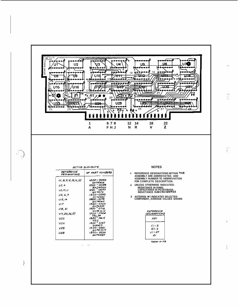
1 6 7 8 12 14 18 22 A F H J N R v z
ACT//YE ELLEMEhlT-5
U/, 8, 9,IZ. Is 14 22
uz, 4
u3, lo, I /
U5,6 ,7
u13,/4
u/ 7
Ul8, ZI
Ul9,ZO,ZC, n U23
U Z 4
UZ5 UZ8
1820- 0055 SN749ON
l820 - 00s SN7400N
/a20 - 0077 SN 74 74
/820- 0099 SN7493h'
/820 -0/74 SU74.WN
/820- 0 0 6 9 SN7420N
I820 - 07/6 SN*l6lN
I 6 2 0 - 0904 93L24
/820 - 0615 9312
I820 - 1/47 SN5419
/8 20- 026/ sN74 / 2 IN
/820- 0214 SN749zN
NOTES
I REFERENCE DESIGNATIONS WITHIN THIS ASSEMBLY ARE ABBREVIATED. ADD ASSEMBLY NUMBER TO ABBREVIATION FOR COMPLETE DESCRIPTION.
2 UNLESS OTHERWISE INDICATED: - . ~~
RESISTANCE IN OHMS; CAPACITANCE IN PICOFARADS INDUCTANCE IN MICROHENRIES
3 ASTERISK (i+) INDICATES SELECTED COMPONENT, AVERAGE VALUES SHOWN
C I - 3 El-3
U I - 2 7 L/
, ,,
Model 5340A Schematic Diagrams
I I l i
I
I I
-1
Figure 8-27. A20 Time Base Assembly
8-53
Model 5340A Schematic Diagrams
Part of Figure 8-28. A21 Control Assembly
STORAGE
ROM ROM u3 u4
- 1) 3 / 3 /
2 , - /
- 4 / 4 /
1 3/ 1 /
STORAGE FF
U14
, 16 ACTIONS TESTS
ACTION-TEST ROM U4 (1816-0004) Truth Table
PRESENT-FUTURE ROM U3 (1816-0003) Truth Table
ACTION I TEST
INPUTS OUTPUTS INPUTS OUTPUTS
ADDRESS E D C B A YB Y71Y6 Y5 Y4:Y3 Y2 Y 1 ADDRESS E D C B A Ye Y7 Y6 Y 5 ! Y 4 Y3 Y2 Y1
PIN NO. 14 13 12 11 10 9 7 i 5 5 4 1 3 2 1 PINNO. 14 13 12 11 10 9 7 6 5 1 4 3 2 1
0 0
2 2 3 3 4 4 0 0 , o o
6 6 0 0 1 1 0
6 O l O O O 0 1 l O O 8 0 1 0 0 0 1 0 0 1 ~ 0 0 0 0 9 0 , 0 0 1 0 9 0 1 0 0 1 1 0 0
1 1 1 I o 0 0 0 0 0 0 1 1 0 0 0 0 1 0 0 0 0 0 0 1 0 1 0 1 : I l : : : 0 0 0 1 1 1 0 0 1 ~ : 1 0 0
1 0 0 1 1 1 0 0 0 5 5 0 0 1 0 , 1 O i l I l 1 1 0
0 0 1 1 ~ 1 0 1 1 7 7 0 0 1 1 1 0 0 1 0 ~ 0 0 0 0
10 10 11 11 12 12 13 13 14 14 15 15 0 1 1 1 1 0 1 1 0 1 0 0 0 0 16 1 0 0 0 0 1 16 , 0 0 0 0 1 1 1 l l O 1 0 0
1 0 0 0 1 1 0 0 1 l 0 0 0 0 16 18 1 0 0 1 0 0 0 0 0 1 0 0 0 0 1 7 17
19 19 1 0 0 l l 0 0 0 20 20 0 1 0 0 1 0 1 : 1 : : : : 21 2, C o 1 0 , , 1 1 0 ' 0 0 1 0 22 22 1 0 1 1 0 0 0 0 0 ~ 0 0 0 0
' 1 : : : : 1 0 1 1 1 1 0 0 1 1 o 1 1 1
1 , 0 0 0 1 1 0 1 ~ 0 0 0 1 1 , 0 0 1 0 1 0 1 ~ 0 1 0 1
23 23 24 24
25 25 26 26 1 1 0 1 0 '
, 1 0 1 1 0 0 0 0
31 31
8-54
'3
I
NOTES
I. REFERENCE DESIGNATIDNS WITHIN THIS ASSEMBLY ARE ABBREVIATED. ADD ASSEMBLY NUMBER TO ABBREVIATION FOR COMPLETE DESCRIPTION.
2. UNLESS OTHERWISE INDICATED: RESISTANCE IN OHMS; CAPACITANCE IN PICOFARADS.
I
Uf
uz u3
I
! I I-
-1
i ..
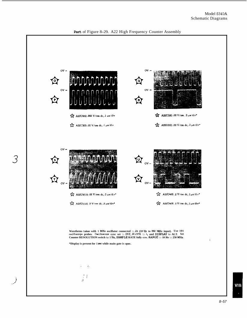
Model 5340A Schematic Diagrams
3
i
Part of Figure 8-29. A22 High Frequency Counter Assembly
& AT2U8(6) .005 V/cm dc, .1 ps/div
fi A22U2(5) .02 V/cm dc, .1 ps/div
@ A22U2(6) .02 V/cm, .2 pe/div*
& A22U2(2) .02 V/cm dc, .2 ps/div*
& AZZUl(13) .06 V/cm dc, .2 d d i v '
a A22U1(15) .2 V/cm dc. .2 @s/div*
& A22U4(6) .2 V/cm dc, 2 ps/div*
fi AZZU4(9) .2 V/cm dc, 2 @s/div*
Waveforms taken with 1 MHz oscillator connected to 54 (10 Hz to 250 MHz input). Use 101 oscillmcope probes. Oscilloacope sync set to INT, SLOPE to +, and DISPLAY to ALT. Set Counter RESOLUTION switch to 1 Hz. SAMPLE RATE fully ccw. RANGE to 10 Hz to 250 MHz.
*Display is present for 1 sec while main gate is open.
,' I :I
8-57
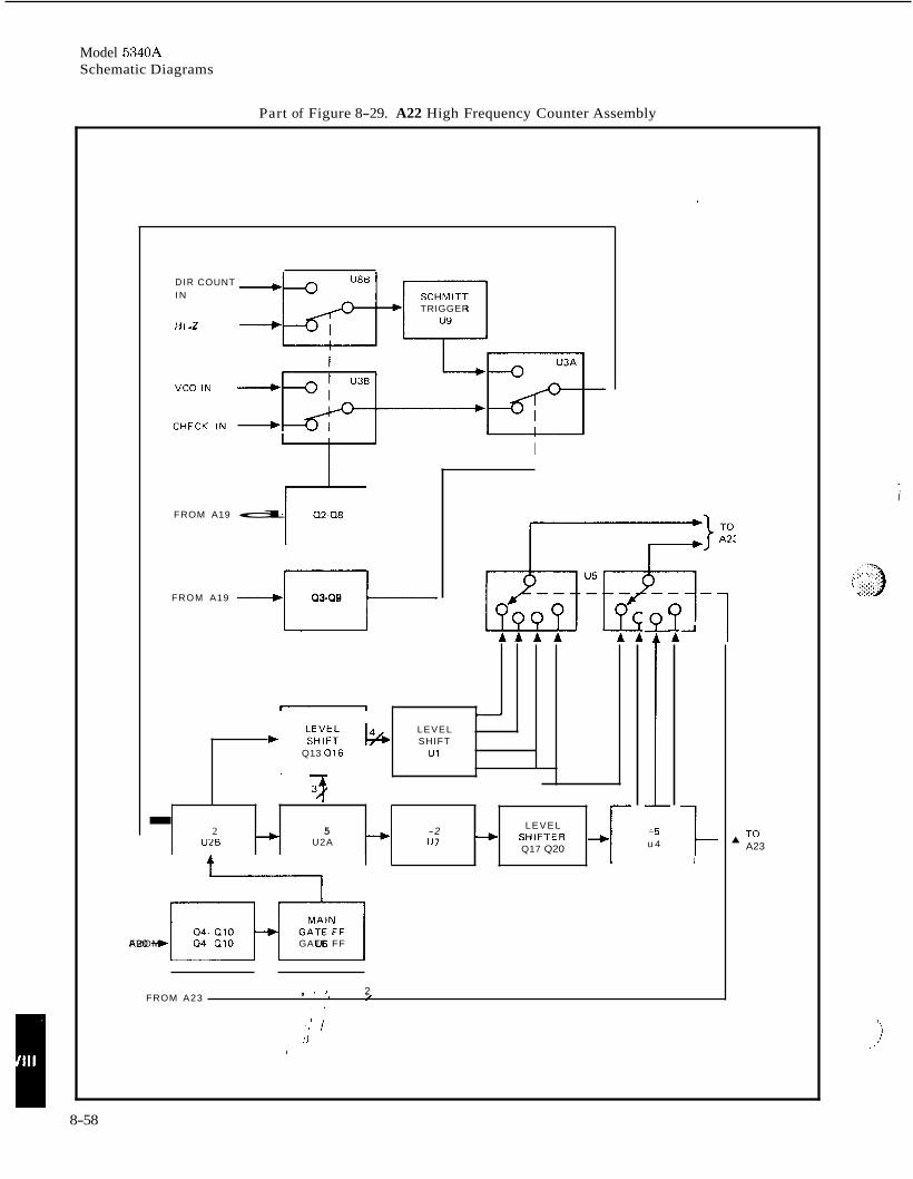
Model 5340A Schematic Diagrams
7
Part of Figure 8-29. A22 High Frequency Counter Assembly
b Q13 0 1 6
D I R COUNT - IN
TRIGGER
HI-2 -
LEVEL SHIFT
u 1
-I-
+ + 2 5 -2 LEVEL + SHIFTER Q17 Q20
- U2B U2A U7
FROM A19 d
F R O M A19 Q3-Q9 El-
+
l
I +5 u 4
A
l- A20+ FROM tT* 0 4 Q10 GATE FF
, ! I , 2, FROM A23 /
, I
To A23
1
i
8-58
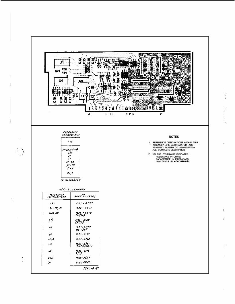
I
A F H J N P R
AC r/vL
CR/
4f - 17, Z/
018, 20
O f 9
Uf
UZ
us, 39 u4
u5
U6,7
u9
5340-0 -2f
NOTES
I. REFERENCE DESIGNATIONS WITHIN THIS ASSEMBLY ARE ABBREVIATED. .ADD ASSEMBLY NUMBER TO ABBREVIATION FOR COMPLETE DESCRIPTION.
2. UNLESS OTHERWISE INDICATED: RESISTANCE IN OHMS; CAPACITANCE IN PICOFARADS: INWCTANCE IN MICROHENRIES
t
I
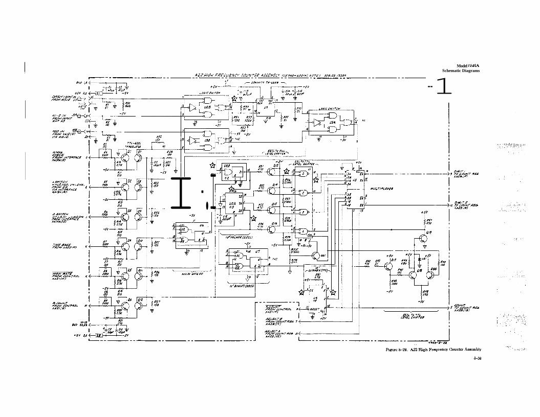
I -.I
Model 5340A Schematic Diagrams
--1
I
I I
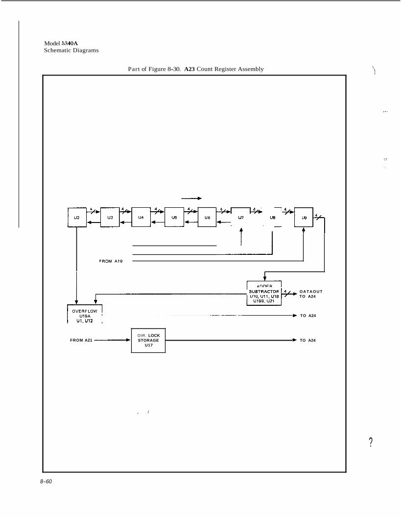
Model 5340A Schematic Diagrams
U6
Part of Figure 8-30. A23 Count Register Assembly
U 7 U8 -
FROM A21 - SUBTRACTOR 4 O A T A O U T u10 , u11. U18 k TO A24
OIR. LOCK STORAGE b TO A24
U17
b TO A24 u 1 . u12
, i .
?
8-60
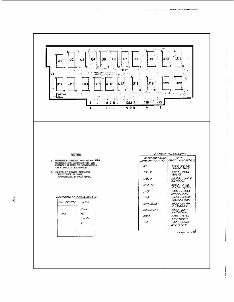
NOTES
I. REFERENCE OESIGNATIONS WITHIN THIS ASSEMBLY ARE ABBREVIATED. ADO ASSEMBLY NUMBER TO ABBREVIATION FOR COMPLETE DESCRIPTION
2. UNLESS OTHERWISE INDICATED: RESISTANCE IN OHMS; CAPACITANCE IN PICOFARADS.
1 I 53+a - 0 -3F
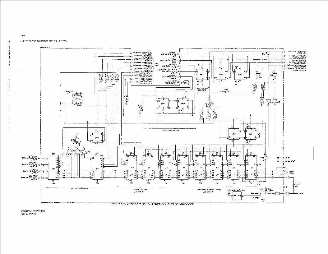
r
I / I I
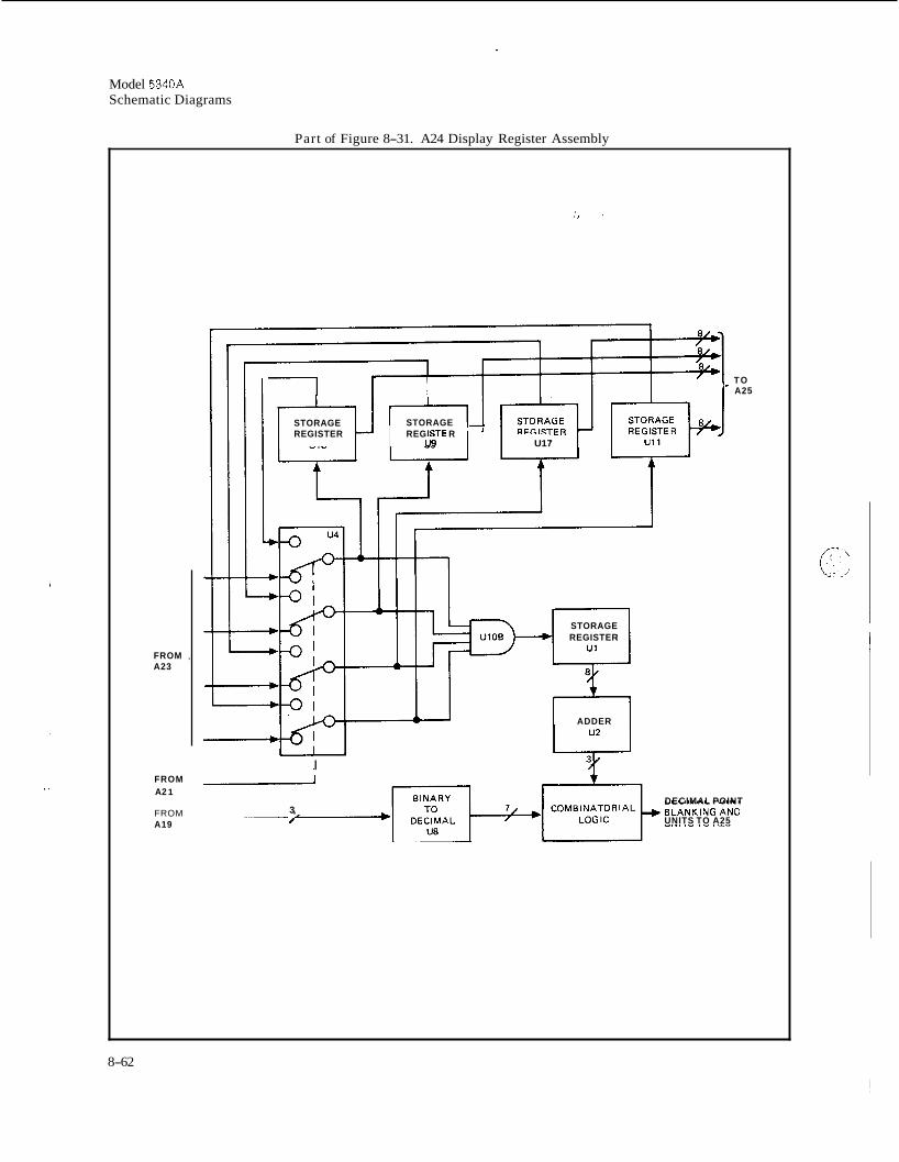
Model 5340A Schematic Diagrams
Part of Figure 8-31. A24 Display Register Assembly
FROM , A23
FROM A2 1
FROM A19
STORAGE REGISTER
1 STORAGE REG ISTE R -
u9 U17
STORAGE REGISTER
ADDER
I
T O ' A25
L DECIMAL POINT
/ UNITS TO A25 3,
8-62
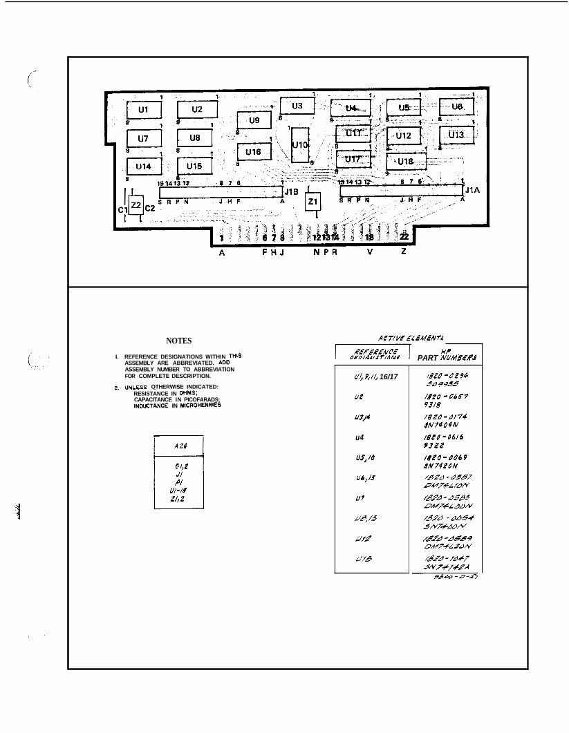
NOTES
I. REFERENCE DESIGNATIONS WITHIN THIS ASSEMBLY ARE ABBREVIATED. ADD ASSEMBLY NUMBER TO ABBREVIATION FOR COMPLETE DESCRIPTION.
D I I N I ESS OTHERWISE INDICATED: -. -. - . RESISTANCE IN OHMS; CAPACITANCE IN PICOFARADS; INWCTANCE IN MICROHENRIES
U/// 9, 16/17
UQ
U3j4
u4
us, 10
U6, /S
U?
U', 13
U Y Z
Uf0
UP PART NUMBERS
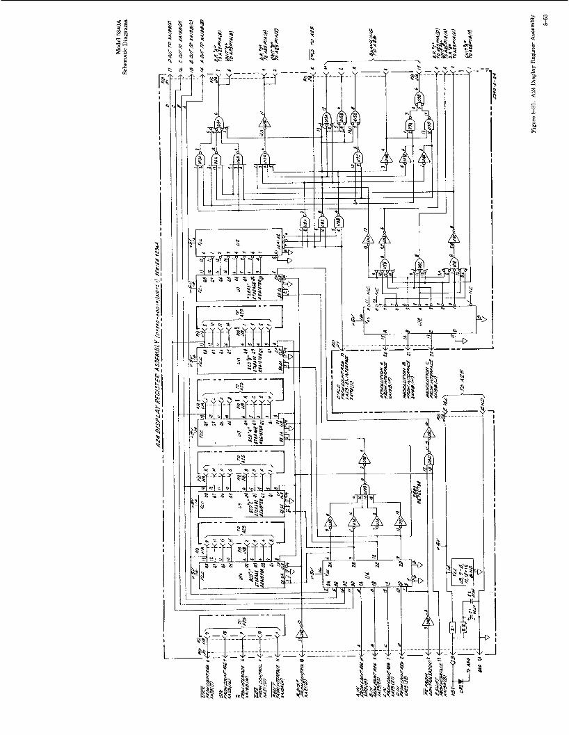
r-----1
1 1
.--
I
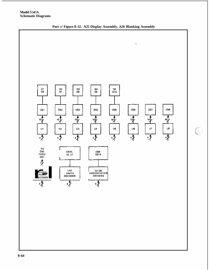
Model 5340A Schematic Diagrams
Part of Figure 8-32. A25 Display Assembly, A26 Blanking Assembly
I .
9
TO DS2
THRU DS7
DECIMAL POINT r-l DECODER
DS15. 16, 17
u 1 0 1 UNITS I DECODER
ANNUNCIATOR DRIVERS
8-64
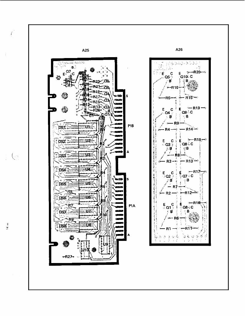
I! '"!
A25 A26
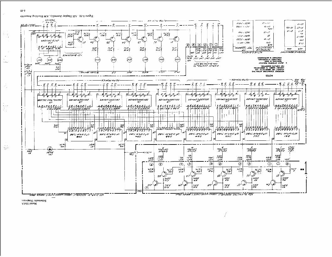
I
I I
I I
9"
1
--1 I I
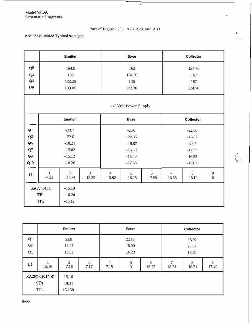
Model 5340A Schematic Diagrams
Emitter Base
Q2 164.8 162
Q4 135 134.70
Q6 133.25 135
Q9 133.05 133.36
Part of Figure 8-33. A28, A29, and A30
A28 05340-60022 Typical Voltages
/ . Collector
134.70
167
167
134.70
Emitter Base
-15 Volt Power Supply
Collector
1 2 3 4 -7.53 -15.91 -18.25 -15.92
-23.7
-23.0
-18.24
-15.82
-15.12
-18.26
5 6 7 8 9 -18.25 -17.89 -16.55 -15.12 0
-23.0
-22.36
-18.87
-16.53
-15.49
-17.53
XA28( 14,R)
TP1
TP2
-22.36
-18.87
-23.7
-17.53
-16.53
-15.82
-15.19
-18.24
-15.12
Emitter Base
Q1 22.8 22.16 Q2 18.27 18.90
Q3 15.52 16.23
1 2 3 4 5 6 15.16 7.16 7.17 7.18 0 16.23
Collector
18.92
23.57
18.31
7 8 9 18.31 18.31 17.40
XA29(14,R,15,S)
TP1
TP2
8-66
15.16
18.31
15.158
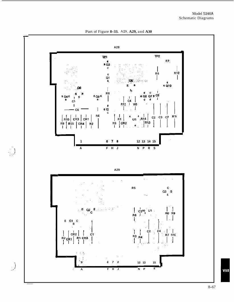
Model 5340A Schematic Diagrams
Part of Figure 8-33. A28, A29, and A30
A28
TP2 'FR1 t R7,
I I
so3
R12 I 1
C
E R6
E
a1 C.
P * B 010 C
I ps % s
EQ4C , p R8
,tgc I c1 B
I 1E
C6 - I R!lO I CkB 1 C k l I R4
- C
R9 R15 CR4 I I , I I I T I
1 6 1 8 12 13 14 15
A F H J N P R S
A29
E Q1 C B
R5 C Q 3 B
' . E
12 13 15 I 6 7 0 I I
I A F H J N P s
~
8-67
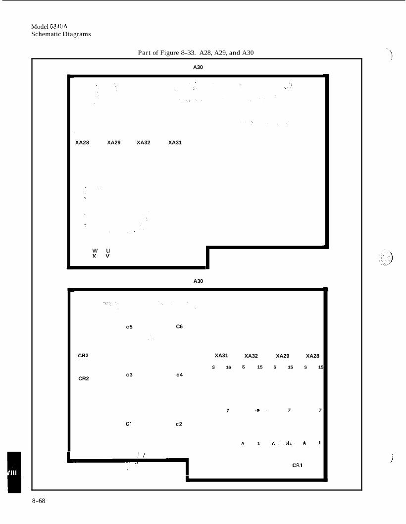
Model 5340A Schematic Diagrams
Part of Figure 8-33. A28, A29, and A30
A30
XA28 XA29 XA32 XA31
. .
w u x v
A30
c5 C6
CR3 XA31
S 16
c3 c4 CR2
7
c1 c2
XA32
S 15
*+
A 1
XA29 XA28
S 15 S 15
7 7
L
i
8-68
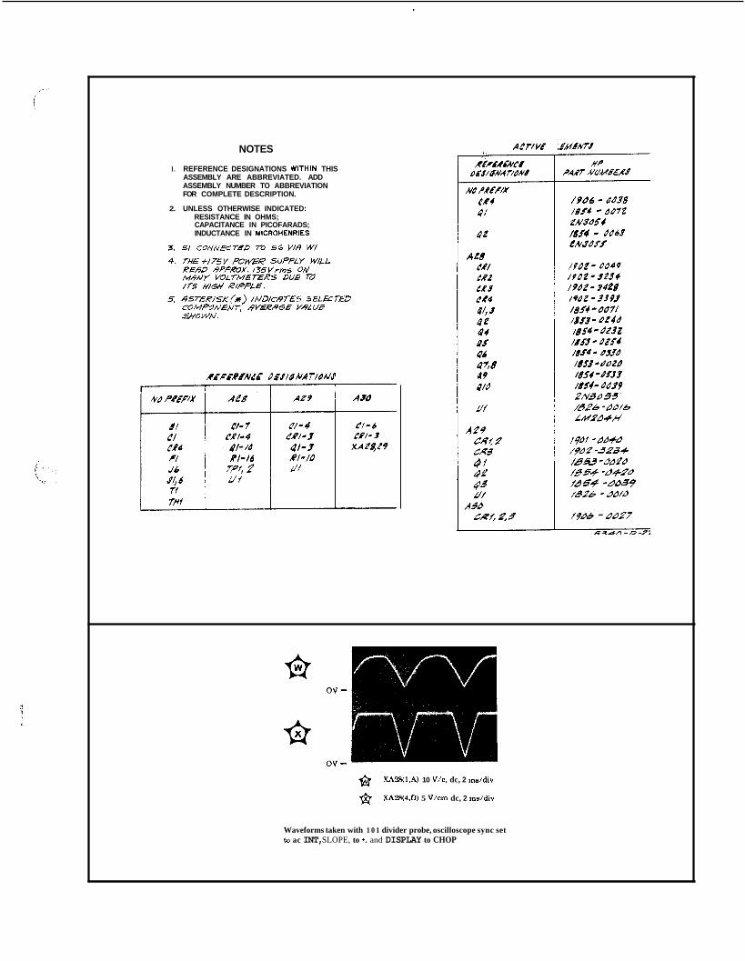
NOTES
I. REFERENCE DESIGNATIONS WITHIN THIS ASSEMBLY ARE ABBREVIATED. ADD ASSEMBLY NUMBER TO ABBREVIATION FOR COMPLETE DESCRIPTION.
2. UNLESS OTHERWISE INDICATED: RESISTANCE IN OHMS; CAPACITANCE IN PICOFARADS; INDUCTANCE IN MICROHENRIES
AC?/V€
& &
XA28(1,A) 10 V/c. dc, 2 ms/div
XA2lX4.D) 5 V / c m dc, 2 ms/div
Waveforms taken with 1 0 1 divider probe, oscilloscope sync set to ac INT, SLOPE, to +, and DISPLAY to CHOP
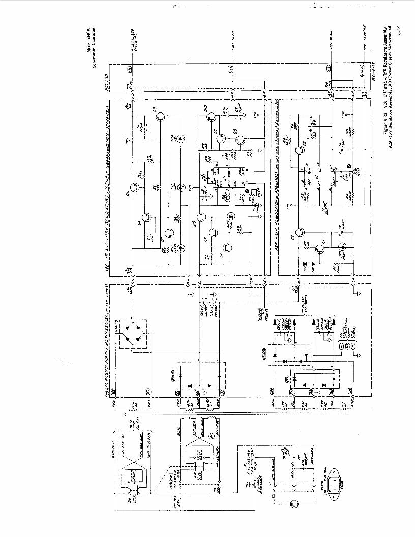
f e P 1
. -
I
1
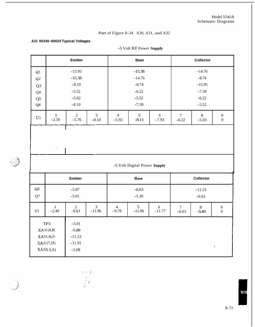
Model 5340A Schematic Diagrams
Q1
Q2
Q3
Q4
Q5
Q8
u1
Part of Figure 8-34. A30, A31, and A32
Emitter Base Collector
-15.95 -15.38 -14.76
-15.38 -14.76 -8.74
-5.52 -6.22 -7.39
-8.10 -8.74 -15.95
-5.02 -5.52 -6.22
-8.10 -7.39 -5.52
1 2 3 4 5 6 7 8 9 -2.50 -5.76 -8.10 -5.92 -8.11 -7.93 -6.22 -5.03 0
A31 05340-60024 Typical Voltages
-5 Volt RF Power Supply
Emitter Base
Q6 -5.87 -6.63
Q7 -5.01 -5.30
1 2 3 4 5 6 u1 -2.49 -9.63 -11.96 -9.78 -11.96 -11.77
Collector
-11.23
-6.63
7 8 9 -6.63 -5.01 0
-5 Volt Digital Power Supply
TP3
XA31(9,K
XA31(7,H)
XA33( 1 ,A)
XA31( 8, J)
-5.01
-5.88
-11.23
-11.91
-5.08
8-71
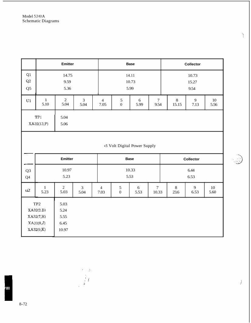
Model 5340A Schematic Diagrams
Emitter Base
Q1 14.75 14.11
Q2 9.59 10.73
Q5 5.36 5.99
Collector
10.73
15.27
9.54
u1 I 1
1 2 3 4 5 6 7 8 9 10 5.10 5.04 5.04 7.05 0 5.99 9.54 15.15 7.13 5.56
- - Q3
Q4
TPl
XA32(13,P)
u2
5.04
5.06
+5 Volt Digital Power Supply
Emitter Base
10.97 10.33
5.23 5.53
Collector
6.44
6.53
TP2 XA32(2,B)
XA32(7,H)
XA32(8,J)
XA32(9,K)
1 2 3 4 5 6 7 8 5.23 5.03 5.04 7.03 0 5.53 10.33 23.6
5.03 5.24
5.55
6.45
10.97
9 10 6.53 5.60
8-72
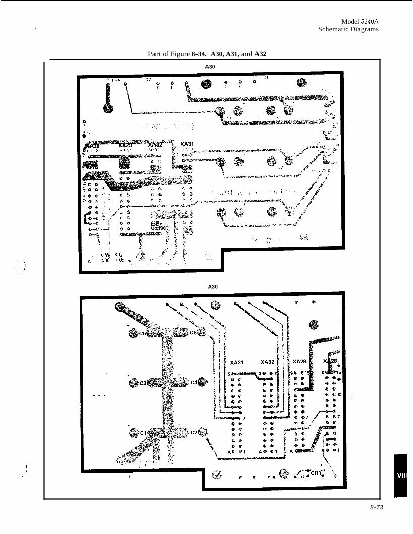
Model 5340A Schematic Diagrams
Part of Figure 8-34. A30, A31, and A32
A30
A30
8-73
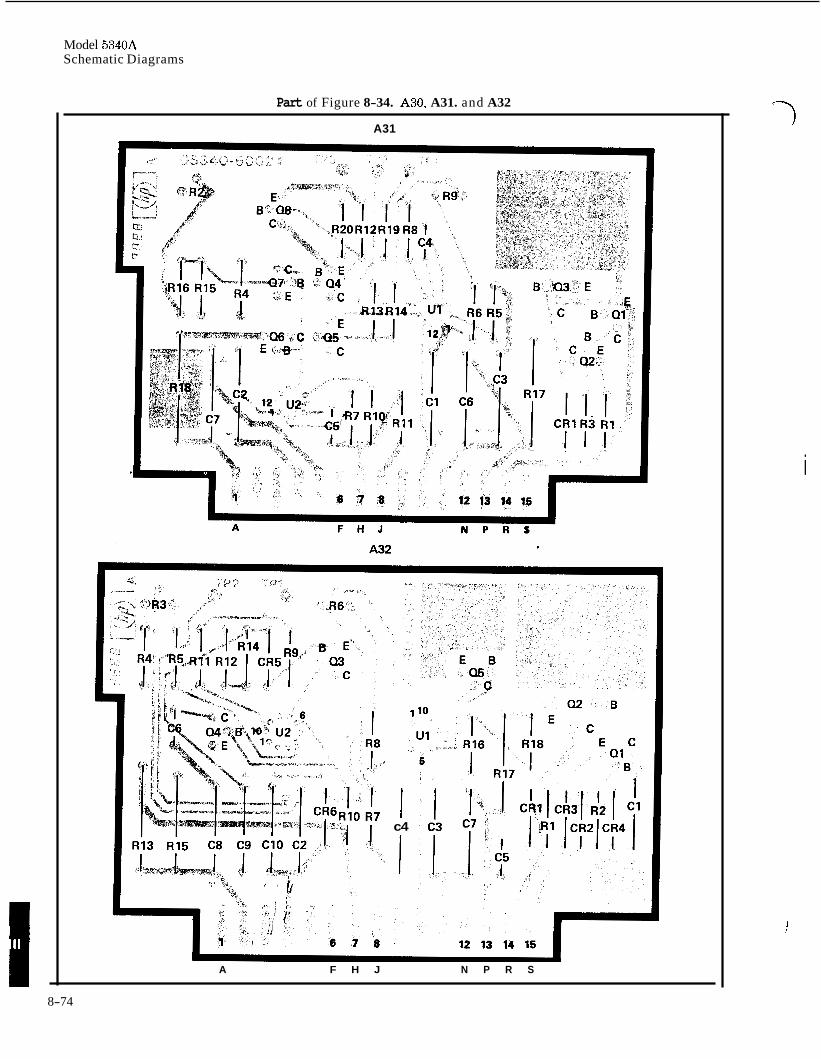
Model 5340A Schematic Diagrams
Part of Figure 8-34. A30, A31. and A32
A31
I c4
I
A F H J N P R S
7
i
i
8-74
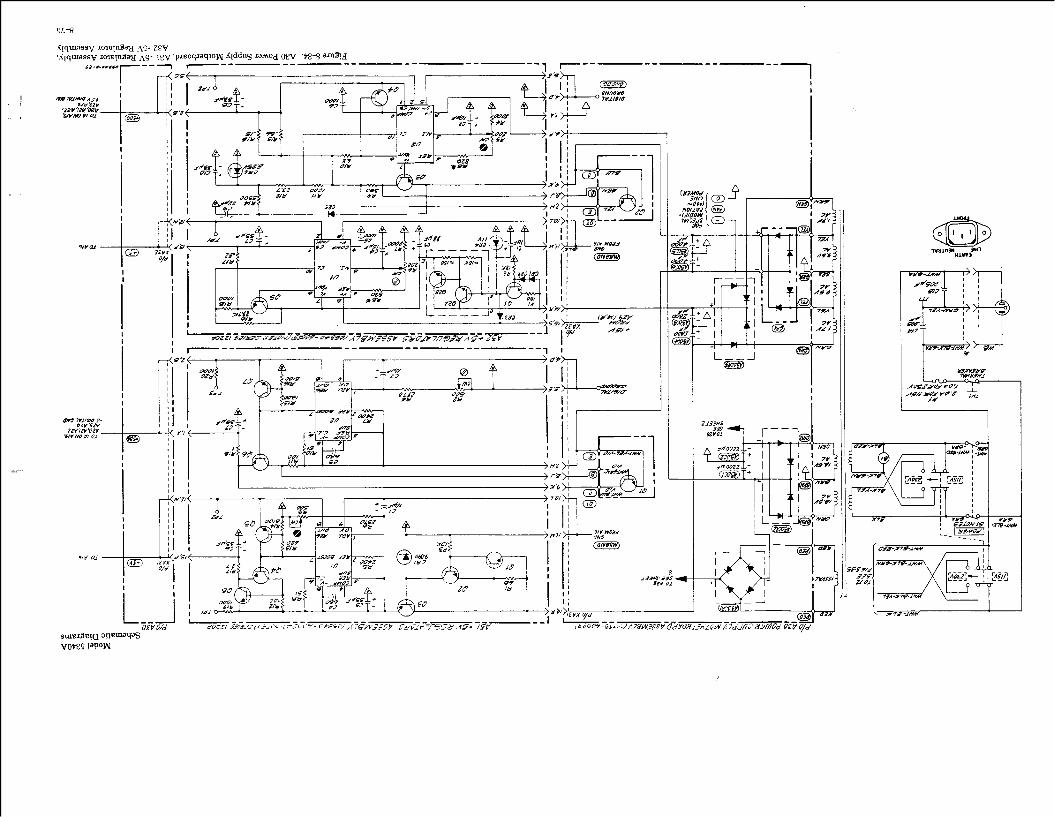
! - :
~.
. ..
. .. ...
I I
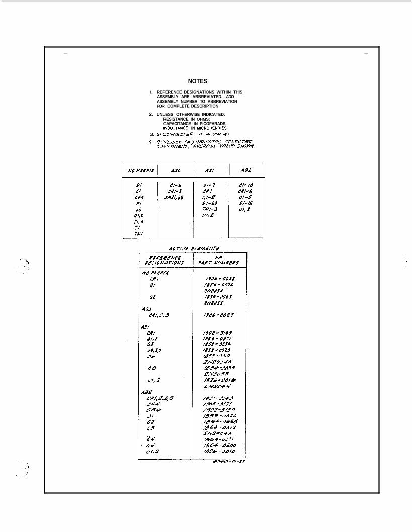
NOTES
I. REFERENCE DESIGNATIONS WITHIN THIS ASSEMBLY ARE ABBREVIATED. ADO ASSEMBLY NUMBER TO ABBREVIATION FOR COMPLETE DESCRIPTION.
2. UNLESS OTHERWISE INDICATED: RESISTANCE IN OHMS; CAPACITANCE IN PICOFARADS, INDUCTANCE IN MICROHENRIES
3. S/ CONA‘ECI€P 7% 56 Y/R W/
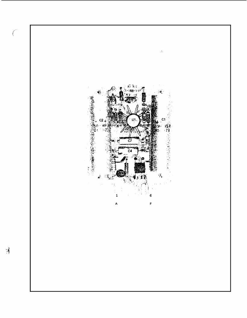
1 6
A F
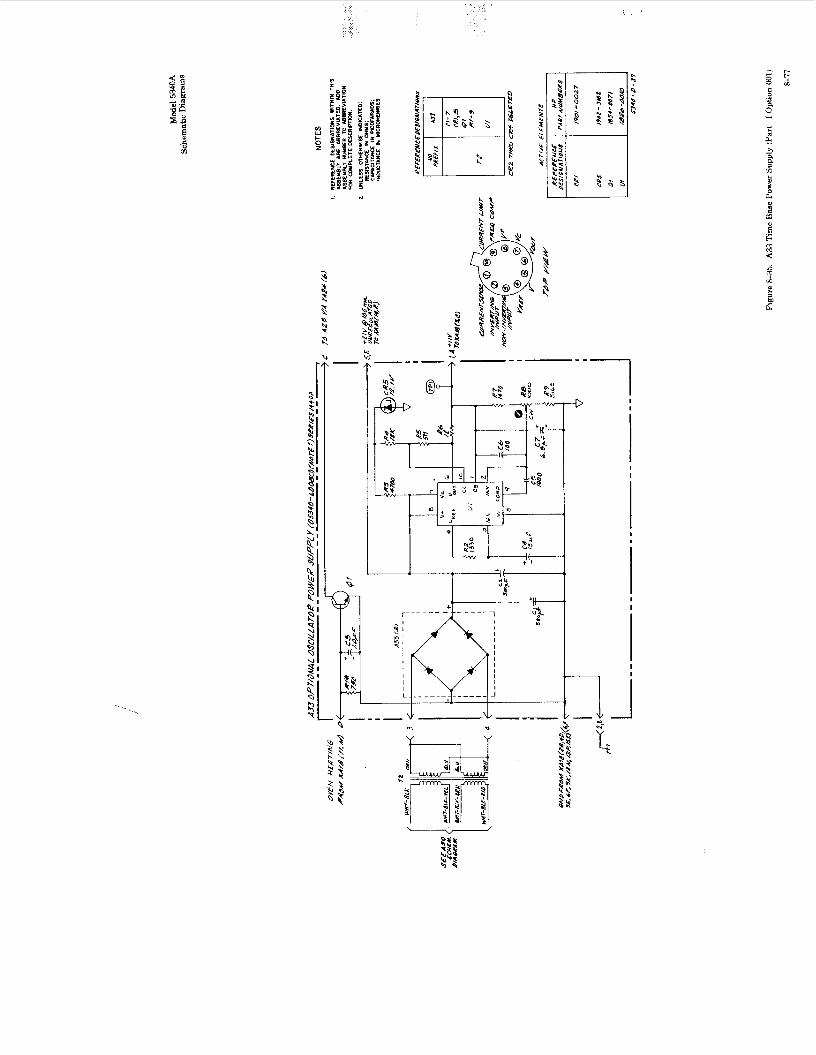
-' N
c
m s
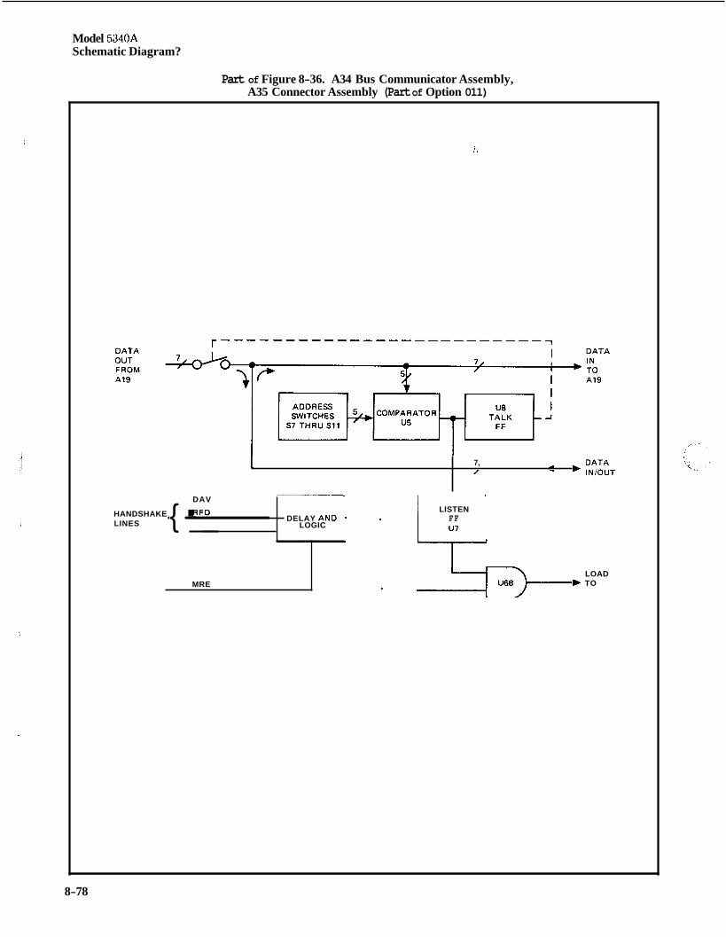
Model 5340A Schematic Diagram?
1
Part of Figure 8-36. A34 Bus Communicator Assembly, A35 Connector Assembly (Part of Option 011)
7, DATA /
1 7 INIOUT
DAV
HANDSHAKE . RFD LINES {-- LISTEN
DELAY A N 0 FF u7 LOGIC
P
8-78
MRE LOAD
b TO
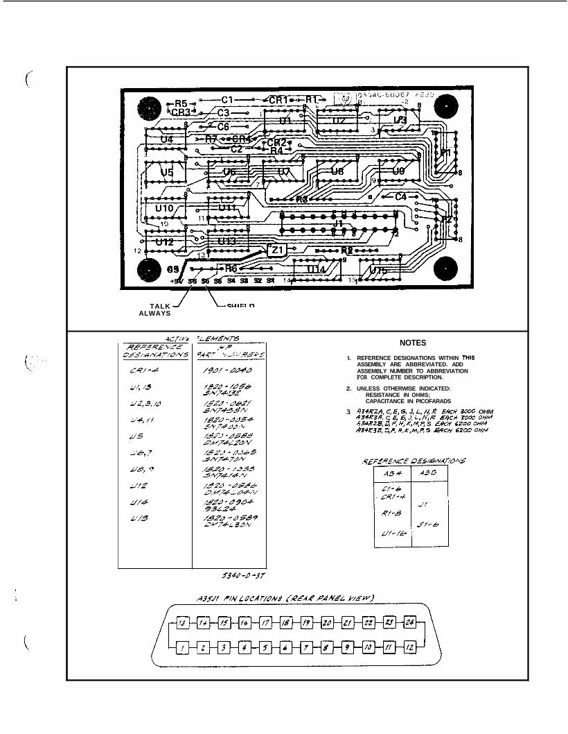
TALK ALWAYS
NOTES
I. REFERENCE DESIGNATIONS WITHIN THIS ASSEMBLY ARE ABBREVIATED. ADD ASSEMBLY NUMBER TO ABBREVIATION FOR COMPLETE DESCRIPTION.
2. UNLESS OTHERWISE INDICATED: RESISTANCE IN OHMS; CAPACITANCE IN PICOFARADS
3. R34RP4, C, E, G, J, L, N R E&M 3000 OHM 434R38, C, E, 6 J, I , N,'R McM MW OHM A B R Z B , 4 F, H,'X, M, F: S E k H 6200 OHM A34R3W,QF,U,K,M,P,S bsCH 6200 OHM
I
I
I
I /
I l l
- - - - - - - -
ii u uh?
w ina
Related Documents