EMEC-I LAB EEE 451 EXPERIMENT NO- 1 OBJECT: To obtain magnetizing characteristics of dc shunt generator. THEORY: Let us consider the saturation curve of shunt generator at a given speed .The maximum EMF by a shunt generator is is given by the point of intersection of the shunt field resistance line, & the open ckt. characteristic curve. Consequently, the maximum EMF generated is Qα However, if the shunt field resistance is increased to the value (represented by the line OB), then the maximum generated EMf is represented by Ob. If we further increase the field resistance to line represented by OC, so that it becomes tangent to the curve. The value of field resistance corresponding to the point of intersection of the field resistance line,& the tangent to the saturation curve, is called the critical field resistance (Rc)for a given speed. APPARATUS REQUIRED: S.N. Name of Equipment Qty. Range CIRCUIT DIAGRAM; OBSERVATION TABLE: S. N. PROCEDURE: CALCULATION: 1

Welcome message from author
This document is posted to help you gain knowledge. Please leave a comment to let me know what you think about it! Share it to your friends and learn new things together.
Transcript

EMEC-I LABEEE 451
EXPERIMENT NO- 1
OBJECT: To obtain magnetizing characteristics of dc shunt generator.
THEORY: Let us consider the saturation curve of shunt generator at a given speed .The maximum EMF by a shunt generator is is given by the point of intersection of the shunt field resistance line, & the open ckt. characteristic curve. Consequently, the maximum EMF generated is Qα However, if the shunt field resistance is increased to the value (represented by the line OB), then the maximum generated EMf is represented by Ob. If we further increase the field resistance to line represented by OC, so that it becomes tangent to the curve. The value of field resistance corresponding to the point of intersection of the field resistance line,& the tangent to the saturation curve, is called the critical field resistance (Rc)for a given speed.
APPARATUS REQUIRED:
S.N. Name of Equipment Qty. Range
CIRCUIT DIAGRAM;
OBSERVATION TABLE:
S. N.
PROCEDURE:
CALCULATION:
RESULT:
PRECAUTIONS;1. Initially keep the load at zero position.2. Increase the load unto rated current only.
ANSWER THE FOLLOWING QUESTIONS:
Q:- How is the voltage build up of d.c shunt generator affected by the variation of speed of the prime mover?
1
EXPERIMENT NO - 2 OBJECT: To obtain efficiency & voltage regulation of a single phase transformer by Sumpner’s back to back test.
THEORY:This test is very useful for high rating transformer as it prevents us to give full load by means of a suitable load impedance.When primary windings of two identical transformers are connected in parallel & are supplied rated voltage & frequency while secondary windings are connected in opposite phase sequence, the voltage across the two secondaries is zero, when primary windings are energized . At this time Wattmeter of primary side reads core losses, when full load secondary current is allowed to flow through secondary windings, Wattmeter of secondary side reads copper losses while Wattmeter of primary side keep on reading core losses.This test requires two identical transformer having their primary connected in parallel & are supplied rated voltage & frequency. When secondaries are open the wattmeter W1 reads the core loss of both the transformers. The two secondaries are connected in series with their polarities in phase opposition which can be checked by the voltmeter connected across a b, Zero reading of the voltmeter indicate s the secondaries are connected in phase opposition. If the terminal a b are short-circuited the current in the secondaries would be zero because Vab = 0 & W1 remains unaltered.Now, a voltage is injected in the secondaries till the rated current flows in the two series connected secondaries.If the readings of wattmeter are W1,W2 and PC & PSC are the core& copper losses of each transformer then,
W1 = 2 PC & W2 = 2PSCNow, the efficiency can be determined by :
Efficiency at full load = 1- (PC + PSC) / {(rated VA) cos02 + PC + PSC}Efficiency at n times of full load = 1- (PC + n2PSC) / {n(rated VA) cos02 + PC + n2PSC}Where, n2 = PC/ PSC
APPARATUS REQUIRED:
S.N. Name of Equipment Range /Rating Qty
CIRCUIT DIAGRAM:
2

PROCEDURE:
OBSERVATION:S.No. W1 W2
CALCULATION:
RESULT:
PRECAUTION:
ANSWER THE FOLLOWING QUESTIONS:
Q:1- Which winding of the transformers are connected in parallel in this test ?
3

EXPERIMENT NO - 3
OBJECT: To plot speed torque characteristics of a dc shunt motor.
THEORY: DC shunt motor is a constant speed motor. When load on the motor is increased, increased load demands are met by producing more torque. Now, when the torque on the motor is increased, Ia also increases. At lower values of Ia, if armature reaction neglected the factor K a( remains constant, the speed decreases due to increase in Te only. But at higher values of armature current, air gap flux reduces due to saturation and armature reaction. Since with the increase of Te, ( is reduced, so factor Te / ( 2
increases. And the speed drops more rapidly.So, we see that the speed of dc shunt motor decreases with load due to increase in Te, and decrease in air gap flux.
APPARATUS REQUIRED:
S.N. Name of Equipment Range /Rating Qty
CIRCUIT DIAGRAM:
PROCEDURE
4

OBSERVATION:
S.No. S1 S2 Radius of pully (R)
CALCULATION:
Applied torque T = (S1 – S2) X g X r Nm
RESULT:
PRECAUTIONS:
ANSWER THE FOLLOWING QUESTIONS:
Q:1-Why does the speed of d.c shunt motor falls slightly when it is loaded?
5

EXPERIMENT NO - 4
OBJECT: To control the speed of dc shunt motor by armature resistance & field flux control method.
THEORY: Speed control by varying the armature terminal voltage is obtained by Ward Leonard method. A separately excited dc motor whose speed is to be controlled is the separately excited generator driven by some prime mover. The combination of dc driving motor and the dc generator is called motor generator set and it converts ac in to dc, which is fed to the main motor. A change in the generator field current varies the voltage applied to the motor armature and, therefore, the motor speed is changed. Thus the motor speed control is obtained merely by changing the generator field current.
APPARATUS REQUIRED:
S.N. Name of Equipment Range /Rating Qty
CIRCUIT DIAGRAM:
PROCEDURE:
OBSERVATION:
S.No. If Vt N rpm
RESULT:
PRECAUTIONS:
ANSWER THE FOLLOWING QUESTIONS:
1-what range of speed can you get with the field control method of speed control of d.c shunt motor?
6

EXPERIMENT NO - 5
OBJECT: To plot load characteristics of dc shunt generator
THEORY: If a dc shunt generator, after building up to its voltage, be loaded , its terminal voltage will drop. This drop, infect increases if load increases but this type of terminal voltage drop is undesirable for a specified services. The relation between terminal voltage and load current is called external characteristics. There are three reasons of voltage drop in dc shunt generator with load
a) Due to armature reaction: Due to demagnetizing effect of armature reaction, pole flux is weakened and induced emf in the armature is decreased.
b) Due to armature resistance drop: As the load current increases, Ia also increases by the relation Ia = IL + Ish, due to which terminal voltage V decreases due to ohmic drop in the armature windings as V = E- Ia Ra
c) Decrease of filed current due to reduction in armature voltage:The drop in terminal voltage due to above two reasons reduces the shunt filed current which decreases filed flux and hence induce emf.
PROCEDURE:
OBSERVATIONS: Speed: ______________
S.No. Generator field current (If) Terminal Voltage (Vt)
RESULT:
PRECAUTIONS:
ANSWER THE FOLLOWING QUESTIONS:
Q:1-Why is the resistance of the field winding of a D.C.Shunt generator kept low?
7

EXPERIMENT NO - 6
OBJECT : To perform open ckt and short ckt test on a 3-phase transformer & determine performer of equipment ckt.
MACHINE SPECIFICATION:
APPARATUS REQUIRED:
S.No. Equipment Range Qty.
THEORY: A load test on 3-phase transformer is necessary to find out its maximum temperature rise. This is only possible if both core loss and full load coppers occurs simultaneously. It is uneconomical and difficult for a large transformer to put on actual full load. Also a suitable load capable of absorbing full load power is not easily available. So indirect full load test or dummy load test is done on a three-phase transformer in laboratory.In this case both primary and secondary windings are delta connected. The LV winding is excited from normal voltage and frequency. The HV winding in open delta is connected to single phase Variac. The voltmeter connected across delta connected winding will read zero. Hence secondary winding behave like open circuit. The sum of W1 and W2 give core loss. Now adjusting the Variac a full current is applied in the secondary side of transformer. Due to this a equipment full load current flows in primary side without effecting wattmeter. Thus W3 gives full load upper loss (W1+W2) still gives core loss.
PROCEDURE:1. Connections are made as per circuit diagram.2. Switch on the 3-phase AC supply to 3-phase transformer.3. Check the voltmeter reading on secondary. It must show zero reading.4. Adjust the Variac on secondary side of transformer till full load current flows in it.5. At this instant record the reading of W1, W2 & W3.
OBSERVATION:
S. No.
W1 W2 W3 Core Loss=(W1+W2) Copper Loss (W3)
RESULT:
Core Loss = ………………………Full load copper loss = ……………………
PRECAUTION:
REPORT:
1. Why load test is done on three phase transformer in laboratory
8

EXPERIMENT NO - 7
OBJECT: To determine polarities on the winding terminals of single phase transformers by polarity test.THEORY: The necessity of three phase system in generation, transmission & distribution is well known to us. Combination of the electrical system & the electromagnetic system of three identical single phase transformers into a single system makes it possible to get a three phase transformer as single unit. Therefore it is interesting to study the different connections in different possible manners. But to study these different connections, ”Polarity” test is primarily required.The polarity of any given terminal of the primary winding is determined by the supply voltage after every half cycle the instantaneous polarity of the terminals of secondary is determined by the direction of flux relative to that of primary terminals. For 1 phase working of T/F is not necessary to find out the polarity, but when to or more single phase T/F are to be connected in parallel or for polyphase operation, it is essential to find out the relative polarities of the winding terminals & mark them
APPARATUS REQUIRED:
S.N. Apparatus Required Range QTY.
CKT DIAGRAM :
PROCEDURE:
OBSERVATION TABLE:
S.N.
CALCULATION:
RESULT:
PRECAUTIONS:
ANSWER THE FOLLOWING QUESTIONS:Q:-What will happen if two transformers are connected in parallel with wrong polarity?
9

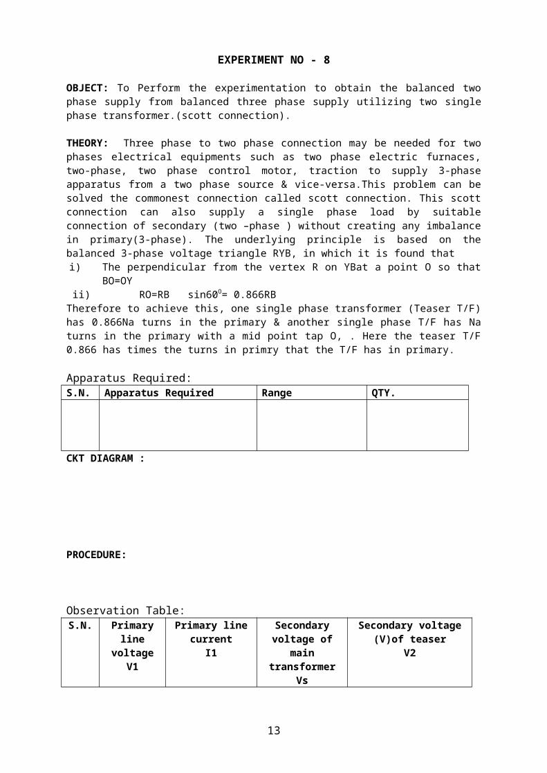
EXPERIMENT NO - 8
OBJECT: To Perform the experimentation to obtain the balanced two phase supply from balanced three phase supply utilizing two single phase transformer.(scott connection).
THEORY: Three phase to two phase connection may be needed for two phases electrical equipments such as two phase electric furnaces, two-phase, two phase control motor, traction to supply 3-phase apparatus from a two phase source & vice-versa.This problem can be solved the commonest connection called scott connection. This scott connection can also supply a single phase load by suitable connection of secondary (two –phase ) without creating any imbalance in primary(3-phase). The underlying principle is based on the balanced 3-phase voltage triangle RYB, in which it is found that i) The perpendicular from the vertex R on YBat a point O so that BO=OY
ii) RO=RB sin60O= 0.866RBTherefore to achieve this, one single phase transformer (Teaser T/F) has 0.866Na turns in the primary & another single phase T/F has Na turns in the primary with a mid point tap O, . Here the teaser T/F 0.866 has times the turns in primry that the T/F has in primary. Apparatus Required:S.N. Apparatus Required Range QTY.
CKT DIAGRAM :
PROCEDURE:
Observation Table:S.N. Primary line
voltageV1
Primary line current
I1
Secondary voltage of main
transformer Vs
Secondary voltage (V)of teaser
V2
CALCULATION:
RESULT:
PRECAUTIONS:
ANSWER THE FOLLOWING QUESTIONS:Q:- 1 How many transformers are needed for scott-connection ?Q:-2 What are the special conditions to be satisfied by the transformers to be used for Scott- connections?
10

EXPERIMENT NO - 9
OBJECT: To obtain load characteristic of a d.c series generator.
THEORY: The field winding (consists necessarily of comparatively few turns of wire having sufficiently large cross-section to carry the rated current of the generator) in the dc series generator is connected in series with the armature the external ckt. The dc series generator, which maintains constant voltage, is used for constant current utility.When the dc series generator is being tested to determine its characteristic, it is assumed that the generator speed is maintained at a constant value i.e., the rated speed of the generator.
Apparatus Required:S.N. Apparatus Required Range Qty.
CKT DIAGRAM:
PROCEDURE:
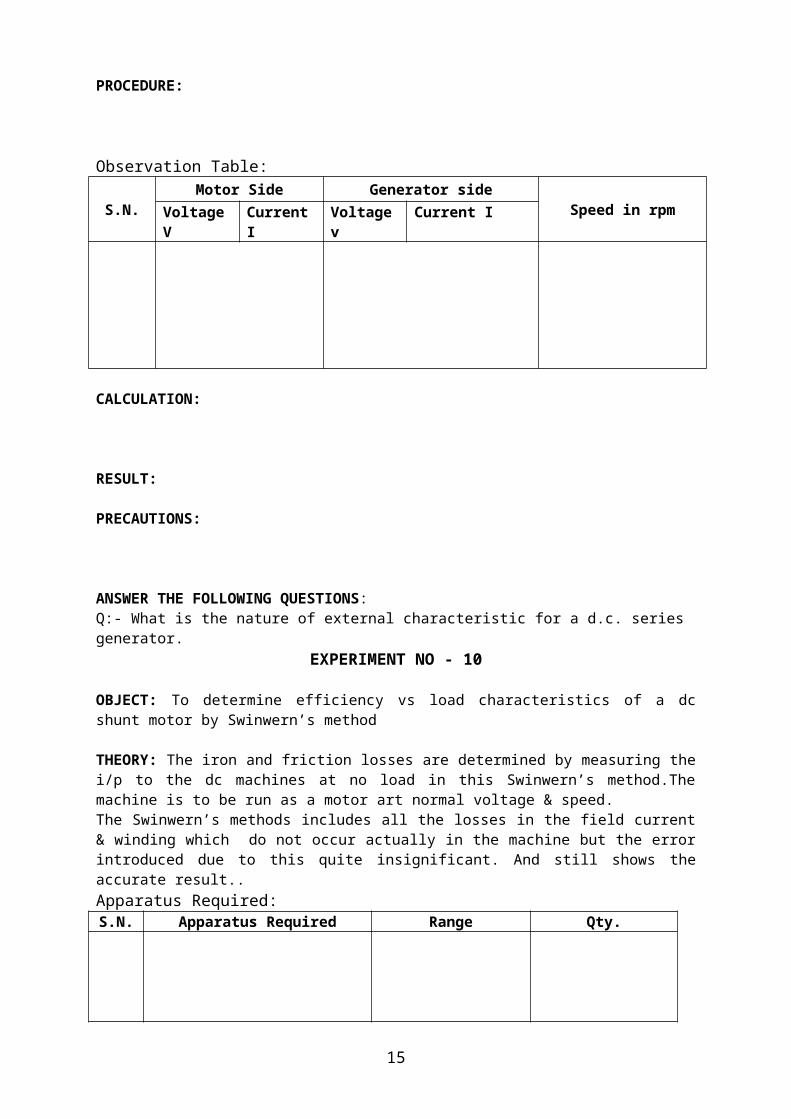
Observation Table:
S.N.Motor Side Generator side
Speed in rpmVoltage V Current I Voltage v Current I
CALCULATION:
RESULT:
PRECAUTIONS:
ANSWER THE FOLLOWING QUESTIONS:Q:- What is the nature of external characteristic for a d.c. series generator.
11

EXPERIMENT NO - 10
OBJECT: To determine efficiency vs load characteristics of a dc shunt motor by Swinwern’s method
THEORY: The iron and friction losses are determined by measuring the i/p to the dc machines at no load in this Swinwern’s method.The machine is to be run as a motor art normal voltage & speed. The Swinwern’s methods includes all the losses in the field current & winding which do not occur actually in the machine but the error introduced due to this quite insignificant. And still shows the accurate result..Apparatus Required:
S.N. Apparatus Required Range Qty.
CKT DIAGRAM :
PROCEDURE:
OBSERVATION TABLE:Table 01
S.N.
Table 02S.N.
CALCULATION:
RESULT:
PRECAUTIONS:
ANSWER THE FOLLOWING QUESTIONS:Q:- Which windings of the transformers are connected in parallel in this test ?
12
NETWORK LABEEE-452
LIST OF EXPERIMENTS
1. To verify Reciprocity Theorem.
2. To verify Superposition Theorem.
3. To verify Thevenin’s, Norton’s and Maximum Power Transfer Theorems.
4. To verify Tellegen’s Theorem.
5. To determine Z- parameter, h- parameter, Y parameter and transmission-parameter of two
port networks.
6. To Study the transient response of RC circuit.
7. To determine Z- parameters of a T- network compute & realize corresponding - network.
8. To verify parameter properties in interconnected two port networks: series, parallel and
cascade.
9. To Study the frequency response of RLC circuit.
10. To study the transient response of R-L-C circuit
11. To measure image and characteristic impedance of T & ∏ network using OC and SC tests
13
EXPERIMENT NO - 1
OBJECT: To verify Reciprocity Theorem.
APPARATUS REQUIRED: S.No. APPARATUS RANGE / RATING Qty MAKE
1
2
3
4
5
Auto transformer
Ammeter
Voltmeter
Rheostats
Connecting Wires
I/p 240 V, 50/60HzO/p 0-240 or 0-270V10 A,0-3 A
0-150-300
0-30 ohms 5.5 A0-210 ohms 1.8 A
1
1
1
21
Hipo Sales
Trinity
Automatic ElectricTrinity
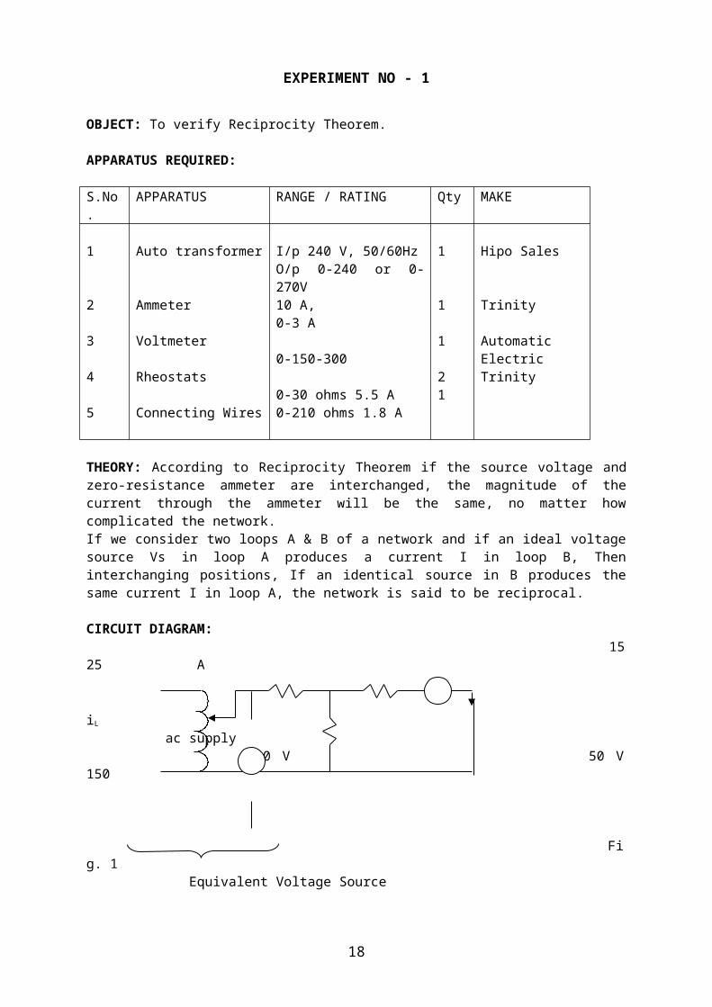
THEORY: According to Reciprocity Theorem if the source voltage and zero-resistance ammeter are interchanged, the magnitude of the current through the ammeter will be the same, no matter how complicated the network.If we consider two loops A & B of a network and if an ideal voltage source Vs in loop A produces a current I in loop B, Then interchanging positions, If an identical source in B produces the same current I in loop A, the network is said to be reciprocal. CIRCUIT DIAGRAM: 15 25 A iL ac supply 230 V 50 V 150
Fig. 1 Equivalent Voltage Source
A 15 25
I’ 150 50 V 230V
Equivalent Voltage Source Fig 2
14
PROCEDURE:
1. Connections are made as per circuit diagram 1.2. A source voltage of 50 and 100 V is applied and Current I is measured and recorded in
the observation table.3. Now connections are made as per circuit diagram 2.4. Again step 2 is repeated and the current measured is I’5. Theoretical values for above circuits are also calculated and are shown in the observation
table. OBSERVATION:
SAMPLE CALCULATION: Theoretically
I = [50/ (15+25 150)] * 150/(150+25) = 1.18 A
I’= [50/ (25+15 150)] * 150/(150+15) = 1.18 A
RESULT/CONCLUSION:
PRECAUTIONS:
15

EXPERIMENT NO -2
OBJECT: To verify Superposition Theorem.
APPARATUS REQUIRED:
S.No.
APPARATUS RANGE / RATING Qty
1
2
3
4
5
Auto transformer
Ammeter
Voltmeter
Rheostats
Connecting Wires
(0 – 260 ) V
( 0 - 3 ) A
( 0 -300 ) V
(0 - 210) Ohms (0 - 30) Ohms
1
1
1
1 2
THEORY: The basic principle of super position states that if the effect produced in a system is directly proportional to the cause, then the over all effect produced in the system due to a number of causes acting jointly, can be determined by superposing (adding) the effect of each source acting separately.The super position theorem is only applicable for linear network & systems.
CIRCUIT DIAGRAM FOR SUPERPOSITION THEOREM:
Z1 Z2 IL V1 Z3 V2
Fig. 2.1
Fig: 2.1(a) To measure current I 1
16
Fig: 2.1(b) To measure current I 2
Fig: 2.1(c) To measure current I’
PROCEDURE:
OBSERVATION:
S.No. V1 V2 iL I1 I2 iL= i1+ i2
I1 is the load current due to V1 & i2 is the load current due to V2
CALCULATION:
RESULT/CONCLUSION:
PRECAUTIONS:
17
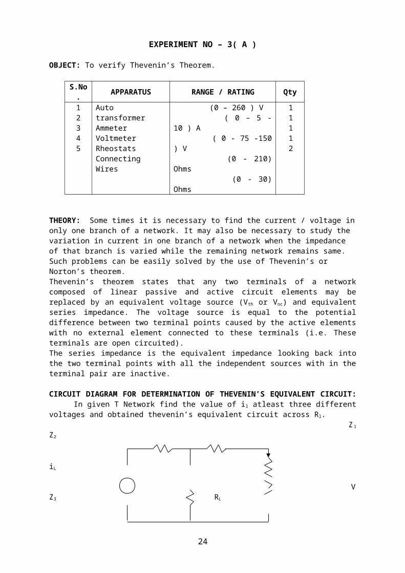
EXPERIMENT NO – 3( A )
OBJECT: To verify Thevenin’s Theorem.
S.No. APPARATUS RANGE / RATING Qty12345
Auto transformerAmmeterVoltmeterRheostatsConnecting Wires
(0 – 260 ) V ( 0 – 5 - 10 ) A ( 0 - 75 -150 ) V (0 - 210) Ohms (0 - 30) Ohms
1 1 1 1 2
THEORY: Some times it is necessary to find the current / voltage in only one branch of a network. It may also be necessary to study the variation in current in one branch of a network when the impedance of that branch is varied while the remaining network remains same. Such problems can be easily solved by the use of Thevenin’s or Norton’s theorem.Thevenin’s theorem states that any two terminals of a network composed of linear passive and active circuit elements may be replaced by an equivalent voltage source (V th or Voc) and equivalent series impedance. The voltage source is equal to the potential difference between two terminal points caused by the active elements with no external element connected to these terminals (i.e. These terminals are open circuited).The series impedance is the equivalent impedance looking back into the two terminal points with all the independent sources with in the terminal pair are inactive.
CIRCUIT DIAGRAM FOR DETERMINATION OF THEVENIN’S EQUIVALENT CIRCUIT:In given T Network find the value of il atleast three different voltages and obtained thevenin’s
equivalent circuit across Rl. Z1 Z2 iL V Z3 RL
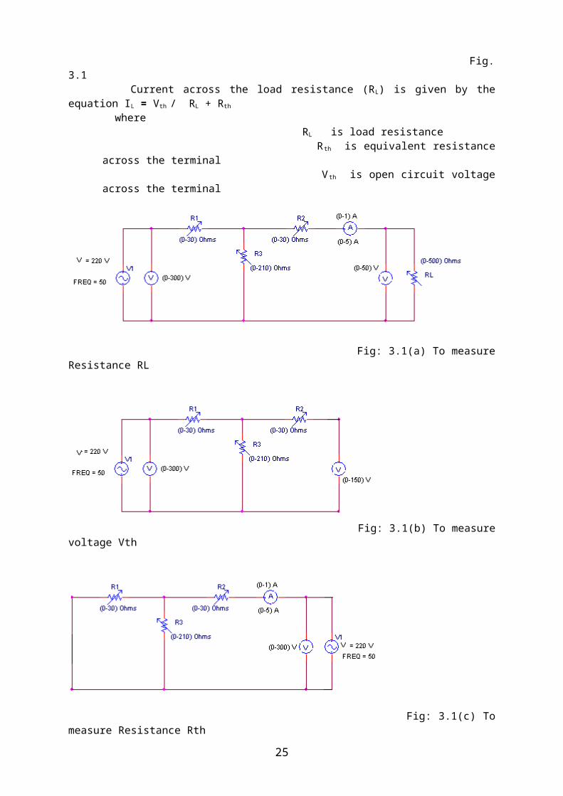
Fig. 3.1 Current across the load resistance (RL) is given by the equation IL = Vth / RL + Rth
where RL is load resistance Rth is equivalent resistance across the terminal Vth is open circuit voltage across the terminal
Fig: 3.1(a) To measure Resistance RL
18

Fig: 3.1(b) To measure voltage Vth
Fig: 3.1(c) To measure Resistance Rth
PROCEDURE:
OBSERVATION:
S.No. Vs iL Vth Zth iL
CALCULATION:
RESULT/CONCLUSION:
PRECAUTIONS:
19

EXPERIMENT NO – 3( B )
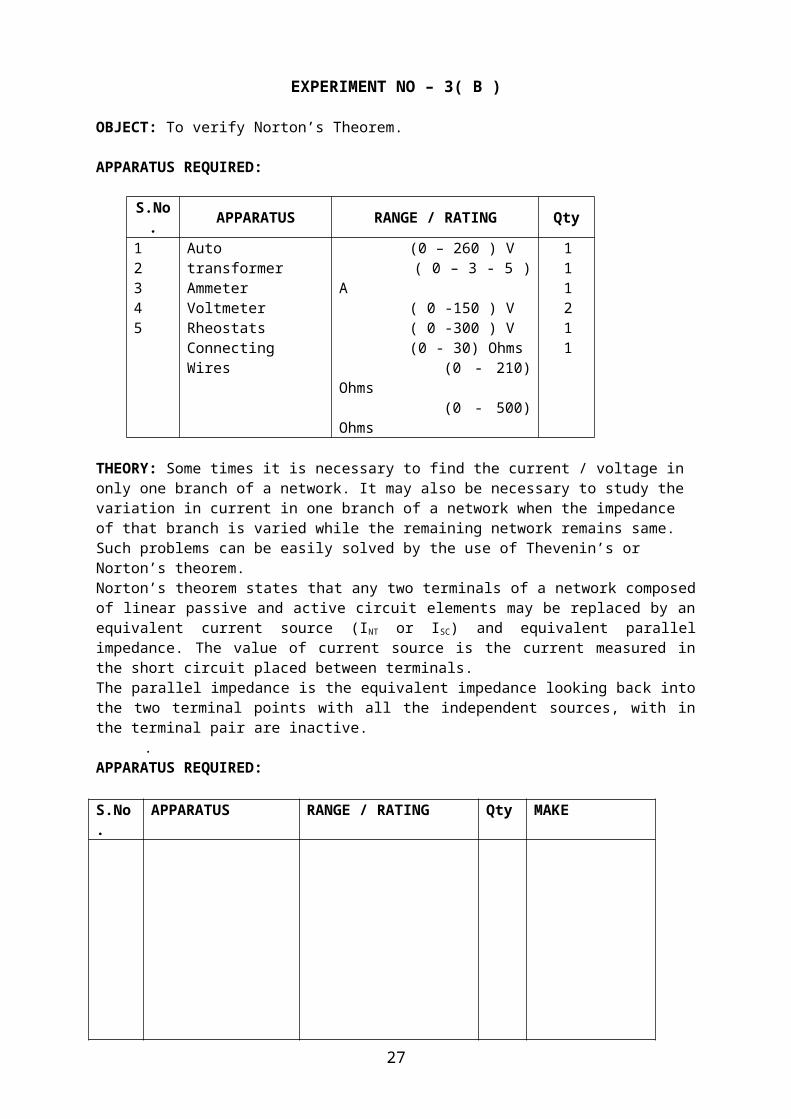
OBJECT: To verify Norton’s Theorem.
APPARATUS REQUIRED:
S.No. APPARATUS RANGE / RATING Qty12345
Auto transformerAmmeterVoltmeterRheostatsConnecting Wires
(0 – 260 ) V ( 0 – 3 - 5 ) A ( 0 -150 ) V ( 0 -300 ) V (0 - 30) Ohms (0 - 210) Ohms (0 - 500) Ohms
1 1 1 2 1 1
THEORY: Some times it is necessary to find the current / voltage in only one branch of a network. It may also be necessary to study the variation in current in one branch of a network when the impedance of that branch is varied while the remaining network remains same. Such problems can be easily solved by the use of Thevenin’s or Norton’s theorem.Norton’s theorem states that any two terminals of a network composed of linear passive and active circuit elements may be replaced by an equivalent current source (INT or ISC) and equivalent parallel impedance. The value of current source is the current measured in the short circuit placed between terminals.The parallel impedance is the equivalent impedance looking back into the two terminal points with all the independent sources, with in the terminal pair are inactive.
.APPARATUS REQUIRED: S.No. APPARATUS RANGE / RATING Qty MAKE
CIRCUIT DIAGRAM FOR DETERMINATION OF NORTON’S EQUIVALENT CIRCUIT: In given T Network find the value of i l atleast three different voltages and obtained Norton’s equivalent circuit across Rl.
Z1 Z2 iL V Z3 RL
Fig. 3.2
20

Fig: 3.2(a) To find the Resistance RL
Fig: 3.2(b) To find the current INT
Fig: 3.2(c) To find the Resistance RNTPROCEDURE:
OBSERVATION:
S.No. Vs iL INT ZNT iL
CALCULATION:
RESULT/CONCLUSION:
PRECAUTIONS:
21

EXPERIMENT NO – 3( C )
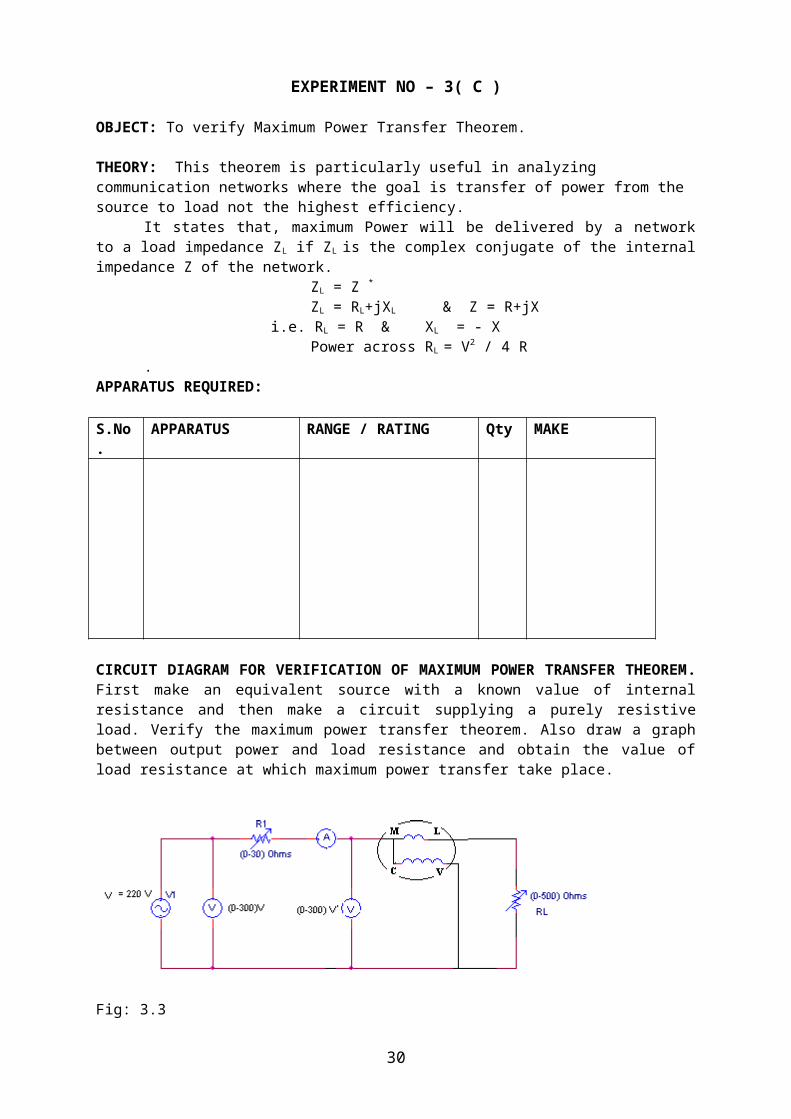
OBJECT: To verify Maximum Power Transfer Theorem.
THEORY: This theorem is particularly useful in analyzing communication networks where the goal is transfer of power from the source to load not the highest efficiency.
It states that, maximum Power will be delivered by a network to a load impedance ZL if ZL is the complex conjugate of the internal impedance Z of the network.
ZL = Z * ZL = RL+jXL & Z = R+jX i.e. RL = R & XL = - X Power across RL = V2 / 4 R.
APPARATUS REQUIRED: S.No. APPARATUS RANGE / RATING Qty MAKE
CIRCUIT DIAGRAM FOR VERIFICATION OF MAXIMUM POWER TRANSFER THEOREM. First make an equivalent source with a known value of internal resistance and then make a circuit supplying a purely resistive load. Verify the maximum power transfer theorem. Also draw a graph between output power and load resistance and obtain the value of load resistance at which maximum power transfer take place.
Fig: 3.3
PROCEDURE:
22

OBSERVATION:
S.No. Vs IL W VL RL= VL/ IL
SAMPLE CALCULATION:
RESULT/CONCLUSION:
PRECAUTIONS:
23
EXPERIMENT NO – 4
OBJECT: To verify Tellegen’s Theorem.
APPARATUS REQUIRED: S.No. APPARATUS RANGE / RATING Qty MAKE
THEORY: Tellegen’s Theorem is essentially a theorem about oriented graphs & hence is valid irrespective of the nature of the circuit elements. Consider a network shown in fig. Which is composed of a two terminal element across which a voltage exists & through which a current flows. In this network, arbitrary reference directions have selected for all of the branch currents & the corresponding branch voltage is indicated , with the positive reference direction at the tail of the current arrow. Now for this network, select a set of branch voltages & a set of branch currents without any consideration the previous choice of branch voltages. The only requirement are that the voltage must satisfy KVL & the KCL be satisfied at each node. Then it can be shown that b VK IK = 0 k = 1 This is the Tellegen’s Theorem.CIRCUIT DIAGRAM FOR TELLEGEN’S THEOREM:
PROCEDURE:
OBSERVATION:
Branch Voltage Branch Current
CALCULATION:
RESULT/CONCLUSION: PRECAUTIONS:
24
EXPERIMENT NO – 5( A )
OBJECT: To determine Z- parameter and y-parameter of two port networks.APPARATUS REQUIRED: S.No. APPARATUS RANGE / RATING Qty MAKE
THEORY: A two-port network is a special case of multi port network. Each port consist of two terminals, one for entry other for exit. In many applications, external connections are made to the terminals of the network only, in pairs. Each pair of terminals would represent an entrance to, or exit from, of a network and is quite descriptively called a “port”. From the definition of a port, the current at entry is equal to that at the exit terminal of a port. In two port networks two linear equations are available in four variables. In a two port networks, one of the ports is called input port 1, while the other is termed, as the output port 2.The port variables are the port currents & port voltages. Z-PARAMETER: Expressing two-port voltages in terms of two port currents V1=Z11 I1 + Z12 I2
V2=Z21 I1 + Z22 I2
Now Z-parameters (open circuit impedance parameters) are;The input driving point impedance with the output port open circuited. Z11=V1/I1 (I2= 0) Forward transfer impedance with the output open circuited. Z21=V2/I1 (I2= 0)Reverse transfer impedance with the input port open circuited. Z12=V1/I2 (I1= 0)The output driving point impedance with the input port open circuited. Z22=V2/I2 (I1= 0)
Y-PARAMETERSExpressing two-port currents in terms of two port currents voltages I1=Y11 V1 + Y12 V2
I2=Y21 V1 + Y22V2
Now Y-parameters (short circuit admittance parameters) are;The input driving point admittance with the output port short-circuited. Y11=I1/V1 (V2= 0)
Forward transfer admittance with the output short-circuited. Y21=I2/V1 (V2= 0)Reverse transfer admittance with the input port short-circuited. Y12=I1/V2 (V1= 0)The output driving point admittance with the input port short circuited. Y22=I2/v2 (V1= 0)
CIRCUIT DIAGRAM: Make a T-network with known values of the resistances. Find Z & Y parameters and compare theoretical and experimental values.
PROCEDURE:
OBSERVATION:
CALCULATION:
RESULT/CONCLUSION: PRECAUTIONS:
25

EXPERIMENT NO – 5( B )
OBJECT: To determine h- parameter and transmission-parameter of two port networks.
Apparatus Required: S.No. APPARATUS RANGE / RATING Qty MAKE
THEORY: h-Parameters: The hybrid parameters would find wide usage in electronic circuits, especially in conducting model of transistors.Voltage of input port and current of output port are expressed in terms of current of input port and voltage of output port V1=h11 I1 + h12 V2
I2=h21 I1 + h22 V2
Now h-parameters are;The input impedance with the output port short-circuited. h11=V1/I1 (V2= 0) Forward current gain with the output short-circuited. h21=I2/I1 (V2= 0)Reverse voltage gain with the input port open circuited. h12=V1/V2 (I1= 0)The output admittance with the input port open circuited. h22=I2/V2 (I1= 0)
TRANSMISSION-PARAMETERSTransmission parameters are used in the analysis of power transmission line, where they are
known as general parameters. The input port is called sending end and the output port is called receiving end. Voltage & current of input port are expressed in terms of voltage and current of output port
V1=A V1 - B V2
I1=C V2 - DV2
Now transmission-parameters (ABCD) are;Reverse voltage gain ratio with receiving end open. A=V1/V2 (I2= 0) Transfer admittance with receiving end open C=I1/V2 (I2= 0)Transfer impedance with receiving end short-circuited. B=V1/(-I2 ), (V2= 0)Reverse current gain ratio with receiving end short-circuited. Y22=I1/(-I2), (V2= 0)
CIRCUIT DIAGRAM: Make a T-network with known values of the resistances. Find h & Transmission parameters and compare theoretical and experimental values. Also check the reciprocity and symmetry of the network.
PROCEDURE:
OBSERVATION:
CALCULATION:
RESULT/CONCLUSION: PRECAUTIONS:
26
EXPERIMENT NO – 6
OBJECT: To Study the transient response of RC circuit.
APPARATUS REQUIRED: S.No. APPARATUS RANGE / RATING Qty MAKE
THEORY: Resistors, capacitors & inductor are the basic elements of any electrical network. Therefore, the study of these elements or either combination for various functions / waveforms is very important. Commonly used functions are step function, impulse function & ramp function.Step function: 1 for t 0 U=
0 for t < 0 Impulse function: The derivative of unit step function is called the impulse function. The behavior of a system with one energy storage element is characterized by a single time constant, which L / R for an inductive circuit & RC for a capacitive circuit. When a system is excited by a internal energy storage the current & voltages decay exponentially to zero from some initial value, at a rate determined by the time constant of the system. The initial value of the variable & the time constant describe the response completely.Impulse Response: When a system is excited by an impulse, energy is stored in the inductance or capacitance in the internal between t = 0 & t = 0+. After its internal, with the circuit left undisturbed, the behavior produced is identical to the natural behavior of the system. Step Response:When the system is excited by a step function the response has a steady state constant value as well as decaying exponential term . This steady state value is the value of function as t approaches infinity. CIRCUIT DIAGRAM: Make circuits and obtain step and impulse response of series and parallel RC circuit. Also draw the theoretical results.
PROCEDURE:
OBSERVATION:
RESULT/CONCLUSION:
PRECAUTIONS:
27

EXPERIMENT NO – 7
OBJECT: To determine Z- parameters of a T- network compute & realize corresponding - network.
APPARATUS REQUIRED: S.No. APPARATUS RANGE / RATING Qty MAKE
THEORY: When a network has three element, these may be arranged as a T- section or a - section. Since the T-section may be redrawn as a star & the -section may be redrawn as a mesh of . The theorem states that at any one frequency, a T- section can be interchanged in any network with a - section & vice- versa, provided certain relation are maintained between the element of two sections. Any impedance of -section is equal to the sum of the product of all possible pair of T-section impedance divided by the opposite impedance of T-section.R1, R2 & R3 are the resistance used in T- network, if Ra, Rb & Rc are the resistance of - network equivalent to given T-network, then Ra = (R1R2 + R2R3 + R3R1) / R1
Rb = (R1R2 + R2R3 + R3R1) / R2
Rc = (R1R2 + R2R3 + R3R1) / R3
CIRCUIT DIAGRAM Make a T-network with known values of the resistances. Find Z parameters and realize corresponding network.
PROCEDURE:
OBSERVATION:
CALCULATION:
RESULT/CONCLUSION:
PRECAUTIONS:
EXPERIMENT NO – 8
28

OBJECT: To verify parameter properties in inter-connected two port networks: series, parallel and cascade.
APPARATUS REQUIRED: S.No. APPARATUS RANGE / RATING Qty MAKE
THEORY: Two-port network in series For network Na and Nb Z parameter equation in matrix form are
V1’ Z11a Z12a I1’ = V2’ Z21a Z22a I2’
V1’’ Z11b Z12b I1’’ = V2’’ Z21 Z22b I2’’ The over all Z parameters are Z11 Z12 Z11a Z12a Z11b Z12b = + Z21 Z22 Z21a Z22a Z21b Z22b Two-port network in ParallelFor network Na and Nb Y parameter equation in matrix form are I1’ Y11a Y12a V1’ = I2’ Y21a Y22a V2’
I1’’ Y11b Y12b V1’’ = I2’’ Y21 Y22b V2’’ The over all Y parameters are Y11 Y12 Y11a Y12a Y11b Y12b = + Y21 Y22 Y21a Y22a Y21b Y22b
Two-port networks in cascade
29
For network Na and Nb Transmission parameters equation in matrix form are
V1’ Aa Ba V2’ = I1’ Ca Da -I2’
V1’’ Ab Bb V2’’ = I1’’ Cb Db -I2’’ Over all transmission parameters are A B Aa Ba Ab Bb = * C D Ca Da Cb Db
CIRCUIT DIAGRAM
PROCEDURE:
OBSERVATION:
CALCULATION:
RESULT/CONCLUSION:
PRECAUTIONS:
30

EXPERIMENT NO – 9
OBJECT: To Study the frequency response of RLC circuit.
APPARATUS REQUIRED: S.No. APPARATUS RANGE / RATING Qty MAKE
THEORY: Frequency response of RLC circuits has many applications based on its frequency selection property, impedance transformation etc in electrical / electronics field.The frequency selection property of the RLC circuit is commonly known as resonance.Series RLC circuit:For a series RLC circuit with a source whose frequency can be varied.Re - Any external resistance may include source resistance.R1 - Coil resistance.R = Re + R1Total impedance Z = R + j (XL - Xc) ---- 1 XL = L Xc = 1 / CXL & Xc are function of time , XL increases with frequency Xc decreases with frequency . The net reactance is the difference of XL & Xc . At low frequency circuit is essentially capacitive as Xc XL . At high frequencies XL Xc , so that circuit becomes inductive. At some frequency Xc = XL & net reactance is zero & the circuit becomes purely resistive circuit. The frequency at which this happens is called the resonant frequency. 0 = 1/ (LC)1/2
f0 = 1/2 1/ (LC)1/2
Z0 = RInput voltage E & current I are in phase at resonance I = E /R , VL = I XL 90 , Vc = I Xc 90 The impedance of the circuit is minimum at resonance so that, the current is maximum. The current decreases on both side of the resonant frequency f0 as shown in fig.1. The sharpness of the curve is seen in terms of a parameter called Quality factor Q. Q = 2 Energy stored in the circuit / Energy dissipated per cycle = Reactive power in L or C / Average power Q = 0L / R = 1/ 0CR Q = 1/R R / (LC)1/2
The quality factor Q = denotes the ability of a circuit to select frequencies close to the resonant frequency & reject all others.Bandwidth: The range of frequencies between cut off frequencies f1 & f2 is called bandwidth. This frequency corresponds to 0.707 of the maximum current.
BW = f2 – f1 = R/2L& Q = f0 / BW
Parallel RLC circuit:
31

Parallel RLC circuit is a more commonly used configuration in electrical / electronic circuits. It is used to transform the impedances so that load & generator impedances are matched for maximum power transfer, as a tuned load at the output of a tuned amplifier. The parallel RLC circuit is also known as a tank circuit due to storage of energy by inductor & capacitor. In ideal case, at resonance the capacitor absorbs energy during one half of the power cycle at same rate at which if being released by the inductor. During next half cycle reverse is true. The total power from the source at this moment is zero. At resonance Impedance is maximum & current I is minimum. CIRCUIT DIAGRAM:
Make RLC Series and parallel circuits and obtain the frequency response and find Bandwidth, Q-factor and resonance frequency .
PROCEDURE:
OBSERVATION:
CALCULATION:
RESULT/CONCLUSION:
PRECAUTIONS:
32

EXPERIMENT NO – 10
OBJECT: To study the Transient response of R-L-C circuit.
APPARATUS REQUIRED: S.No. APPARATUS RANGE / RATING Qty MAKE
THEORY: The conservation of energy is one of the basic laws of the universe. Electric circuits, which contain capacitor and inductor, exhibit cyclical behaviour. Energy is first stored in the electric field of a capacitor, is transferred to the magnetic field of an inductor and then returned to the electric field of the capacitor and so on. The process continues indefinitely until the energy is dissipated by the resistive losses of the system.Impulse Response of R-L-C Series Circuit:The basic differential equation for a circuit can be written in the standard form:
+2 + 2 y=0
The parameters in the equation are= R/2L and 2 = 1/LC
The nature of the response depends on the relative values of and . There are mainly three types of responses
Over Damped Response ( > ) y=A1ep1t + A2 ep2t for t>0 Where p1, 2=-A1 and A2 can be obtained from the initial conditions.
Critically Damped Response ( = ) y=e-αt(A1+A2 t) for t > 0A1 and A2 can be obtained from the initial conditions.
Under Damped Response ( < ) y= e-αt (A1 cos + A2 sin ) for t > 0 y= A e-αt cos( + ) = A1, A, A2 and can be obtained from the initial conditions.
Impulse Response of R-L-C series circuit:Impulse voltage is applied.Impulse Response of R-L-C parallel circuit:Impulse voltage is applied.Step Response of R-L-C series circuit:
33

The step response of series R-L-C circuit differs from the impulse or natural response. A steady state value occurs in the circuit, this added as a constant added to the solution. Constant can be obtained as the value of the function at infinity. i(t)=A1ep1t + A2 ep2t +B for t>0 Where p1, 2=-A1 and A2 can be obtained from the initial conditions.Step Response of R-L-C parallel circuit:The response of a parallel R-L-C circuit to step current source is same as the response of series R-L-C circuit to a step voltage. α=1/2RC
CIRCUIT DIAGRAM:Make series and parallel RLC circuits and obtain the Transient response. Also obtain the response curve theoretically.
PROCEDURE:
OBSERVATION:
CALCULATION:
RESULT/CONCLUSION:
PRECAUTIONS:
EXPERIMENT NO – 11
34

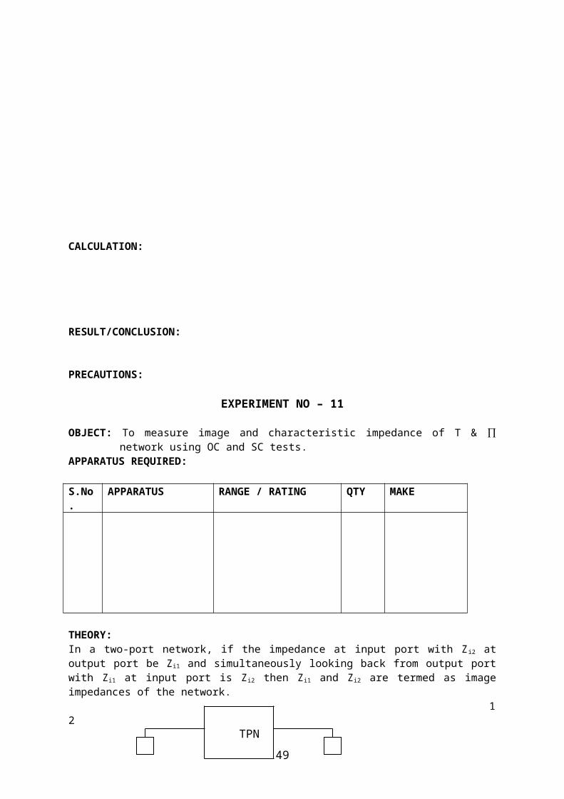
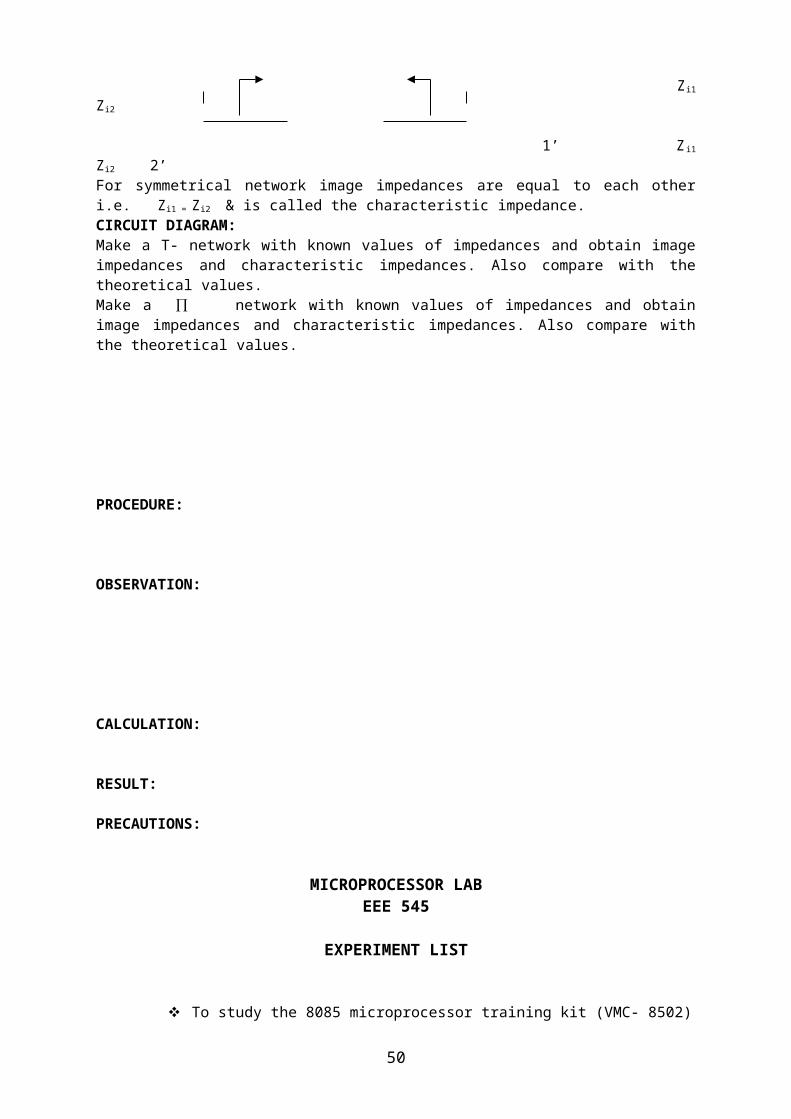
OBJECT: To measure image and characteristic impedance of T & ∏ network using OC and SC tests.
APPARATUS REQUIRED: S.No. APPARATUS RANGE / RATING QTY MAKE
THEORY: In a two-port network, if the impedance at input port with Zi2 at output port be Zi1 and simultaneously looking back from output port with Z i1 at input port is Zi2 then Zi1 and Zi2 are termed as image impedances of the network. 1 2 Zi1 Zi2
1’ Zi1 Zi2 2’ For symmetrical network image impedances are equal to each other i.e. Z i1 = Zi2 & is called the characteristic impedance. CIRCUIT DIAGRAM: Make a T- network with known values of impedances and obtain image impedances and characteristic impedances. Also compare with the theoretical values.Make a ∏ network with known values of impedances and obtain image impedances and characteristic impedances. Also compare with the theoretical values.
PROCEDURE:
OBSERVATION:
CALCULATION:
RESULT:
PRECAUTIONS:
35
TPN
MICROPROCESSOR LABEEE 545
EXPERIMENT LIST
To study the 8085 microprocessor training kit (VMC- 8502)
Study of 8086 microprocessor training kit.
To perform addition of two 8 bit numbers; sum 8 bit
To perform addition of two 8 bit numbers; sum 16 bits.
To perform subtraction of two 8 bit numbers.
To find the largest number from a given number of string.
To find the smallest number from a given number of string.
To perform a string of numbers in ascending order with the help of given string.
To perform a string of numbers in descending order with the help of given string.
To perform multiplication of 8 bit data; Product should be 16 bit.
To perform one’s and two’s compliment of 8 bit numbers.
Interface 8255 PPI to microprocessor and set port A as input port in Mode 0.
Study of Digital to Analog interfacing module with the help of 8086 microprocessor
training kit.
To study the operation of 6264RAM study card with the help of 8085 microprocessor
training kit.
36
EXPERIMENT NO - 1
OBJECT: To study the 8085 microprocessor training kit (VMC- 8502)
APPARATUS REQUIRED: 8085 microprocessor training kit.
THEORY:GENERAL
The system has got 8085 as the central processing unit. The clock freq for the system is 3.07 MHz and is generated from a crystal of 6.14 MHz.
8085 has got 8 data lines and 16 address lines. The lower 8 address lines and 8 data lines are multiplexed. Since the lower 8 address bits appear on the bus during the first clock cycle of a machine cycle and the 8 bit data appears on the bus during the second and third clock cycle, It becomes necessary to latch the lower 8 address bits during the first clock cycle so that the 16 bits address remains available in subsequent cycle. This is achieved using a latch a 74-LS-373.
MEMORY: - VMC-850X provides 2/8k bytes of RAM using 6116-6264 chips and 4k/8k bytes of EPROM for monitor.The various chips which can be used are 2732, 2764, 27128, 27256, 6116 and 6264. There is one memory space provided on VMC 850CX. This one space can be defined any address slots from 3000-FFFF depending upon the size of the memory chip to be used.
INPUT/OUTPUT DEVICES The various I/O chips used in VMC8501 are 8279, 8255 & 8253 and VMC8502 are 8279, 8255, 8253 & 8151.The functional role of all these chips is given below: -
8279 (KEY BOARD AND DISPLAY CONTROLLER): - 8279 is a general-purpose programmable keyboard and display I/O interface device designed
for used with the 8085 microprocessor. It provides a scanned interface to 28 contact key matrixes provided in VMC850X and scanned interface for the six seven segment displays. 8279 has got 16 x 8 display RAM that can be loaded or interrogated by the CPU. When a key is pressed, its corresponding codes are entered in the FIFO queue of 8279 and can now we read by the microprocessor.
8255 (PROGRAMABLE PERIPHERAL INTERFACE): -8255 is a programmable peripheral interface (PPI) designed to used with 8085
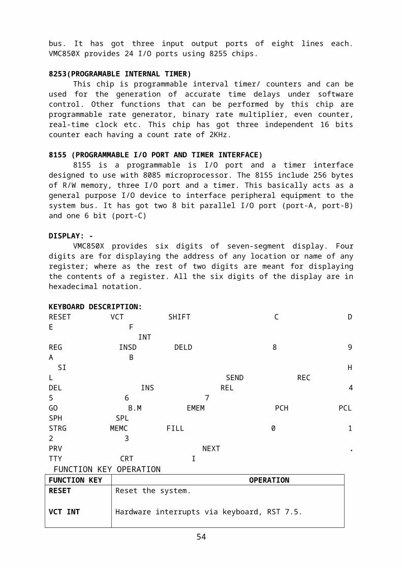
microprocessor. This basically acts as a general purpose I/O devices to interface peripheral equipment to the system bus. It has got three input output ports of eight lines each. VMC850X provides 24 I/O ports using 8255 chips.
8253(PROGRAMABLE INTERNAL TIMER)This chip is programmable interval timer/ counters and can be used for the generation of
accurate time delays under software control. Other functions that can be performed by this chip are programmable rate generator, binary rate multiplier, even counter, real-time clock etc. This chip has got three independent 16 bits counter each having a count rate of 2KHz.
8155 (PROGRAMMABLE I/O PORT AND TIMER INTERFACE)8155 is a programmable is I/O port and a timer interface designed to use with 8085
microprocessor. The 8155 include 256 bytes of R/W memory, three I/O port and a timer. This basically acts as a general purpose I/O device to interface peripheral equipment to the system bus. It has got two 8 bit parallel I/O port (port-A, port-B) and one 6 bit (port-C)
DISPLAY: -VMC850X provides six digits of seven-segment display. Four digits are for displaying the
address of any location or name of any register; where as the rest of two digits are meant for displaying the contents of a register. All the six digits of the display are in hexadecimal notation.
37

KEYBOARD DESCRIPTION:RESET VCT SHIFT C D E F INT REG INSD DELD 8 9 A B SI H L SEND RECDEL INS REL 4 5 6 7GO B.M EMEM PCH PCL SPH SPLSTRG MEMC FILL 0 1 2 3PRV NEXT . TTY CRT I FUNCTION KEY OPERATIONFUNCTION KEY OPERATIONRESET
VCT INT
SHIFT
GO
SI
REG
EMEM
PRE
NEXT
‘ . ’
DEL
INS
BLOCK MOVE
FILL
REL
INSD
DELD
STRG
MEMC0 – F
Reset the system.
Hardware interrupts via keyboard, RST 7.5.
Provides a second level command to all keys.
To execute the program.
To execute the program in single step mode.
Examine register; allows user to examine and modify the contents of different registers.
Examine memory; allows user to examine any memory location and modify any RAM location.
Previous is used as an intermediate terminator in case of Examine memory .It decrements the PC contents and write the contents of data field to the address displayed in the address location.
Increment is used as a intermediate terminator in case of Examine memory, Examine register etc. It increment the PC contents and writes the data lying in data field at the location displayed at address field. Terminator is used to terminate the command and writes the data in data field at the location displayed in address field.
Delete the part of program or data, with relocation by one or more bytes.
Insert the part of program or data, with relocation by one or more bytes.
Allows user to move a block of memory to any RAM area.
Allows user to fill RAM area with a constant.
Relocate a program written for some memory area and to be transferred to other memory area.Insert one or more data bytes in the user’s program / data area.
Deletes one or more data bytes from the user’s program / data area.
Find out the string of data lying at a particular address or addresses.
Memory compare: Compares two blocks of memory for equality.Hexadecimal Keys.
38

PROCEDURE OF RUNNING A PROGRAM
RESETStarting add. Of program [Next] Data . . .End add. of program [Next] Data
FILLRESETStarting add. Of data [Next] Data . . .End adds. Of data [Next] Data
FILLRESETDEL GOStarting add. of programFILLRESETLocation of result [Next]
PRECAUTIONS:
1. Handle the kit carefully.2. Connect the power supply (if needed) carefully.3. Make sure jumpers are positioned correctly and properly.4. Press the MP kit keys properly.
39

EXPERIMENT NO - 2
OBJECT: Study of 8086 microprocessor training kit.
APPARATUS REQUIREMENT: VMC 8603 microprocessor training kit.
THEORY: VMC-8603 is a single board microprocessor training /development kit configured around the INTEL’s 16 bit microprocessor 8086. The kit has been designed to operate in the max mode.
HARDWARE DESCRIPTION
CPU
8086 is a 16 bit, third generation microprocessor and is suitable for an exceptionally wide spectrum of microprocessor applications. 8086 has got 16 bit data lines and 20 address lines.
CO-PROCESSOR 8087
The 8087 coprocessor “hooks’ has been designed into the 8086. a co-processor differ from independent processor in that it obtains its instructions from another processor , called a host. The co-processor monitors instructions fetched by the host and recognizes certain of these as its own and execute them. A co-processor, in effect, extends the instruction set of its host computer.
I/O PROCESSOR 8089
The 8086 is designed to be used with the 8089 in high performance I/O applications.
CLOCK GENERATION
The clock generation circuit is an Intel’s 8284-clock generator/driver. The circuit accepts a crystal input, which operate at fundamental frequency of 14.7456 MHz.The clock generator/driver divides the crystal frequency by three to produce the 4.9 MHz CLK signal required by CPU. The clock generator/driver provides two control signal outputs, which are synchronized (internally) to the 4.9 MHz CLK signals; RDY (ready) and RST (reset).
BUS CONTROLLER
The 8288 is a bus controller which decodes the status signals output by 8089,or a maximum mode 8086.The 8288 issue a bus command that identifies the bus cycle as a memory read, memory write, i/o read, i/o write, etc. It also provides a signal that strobes the address into latches.
BUS ARBITERS
The 8289 is a bus arbiter that controls the access of a processor to a multimaster system resources (typically memory) that is shared by two or more microprocessors.
MEMORY
VMC-8603 provides 16K byte of EPROM loaded with monitor and 16K bytes of CMOS RAM .The total on board memory can be configured as follows. EPROM - 512 bytes of EPROM using 27C010, 1024 bytes using 27C020 & 256K bytes using 62C1024. RAM - 64K bytes of RAM using 62256.
40

I/O DEVICES
82798279 is a general-purpose programmable keyboard and display I/O interface device Designed for use with the 8086 microprocessor. It provides a scanned inter face to 28 channel key matrix provided in VMC-8603 and scanned displays.
8255 8255 is programmable peripheral interface (PPI) designed to use with 8086 microprocessor. This basically acts as a general purpose I/O component to interface peripheral equipments to the system bus.8253This chip is a programmable interval timer/counter and can be used for the generation of accurate time delays under software control. Various other functions that can be implemented with this chip are programmable rate generation.
8251This chip is programmable communication interface and is used as a peripheral device. This device accepts data characters from CPU in parallel form and then converts them into a continuous serial data stream for transmission.
DISPLAYVNC-8603 provides eight digits of seven-segment display. Four digits are for displaying the address of any location or name or any register, whereas the rest of the four digits are meant for displaying the contents of memory location or of a resister. All the eight digits of the display are in hexadecimal notation.
Keyboard description: The VMC-8603 has 28 keys and eight seven segment displays to communicate with outside world. RESET VCT F3 C D E F INTR BC/IP LS/FL VR PRG/INS DEL F2 8 9 A B + _ IW/CS OW/DS /SS /ESREG BS F1 4 5 6 7 : IB/SP OB/BP MV/SI EW/DIFILL CRT TTY 0 1 2 3PRV NEXT . EB/AX ER/BX GO/CX ST/DX
41

HEXADECIMAL KEYPAD LEGEND INTERPRETATION
HexadecimalKey
Acronym Command name Acronym Resister name
0 EB/AX 1 ER/BX 2 GO/CX 3ST/DX
4IB/SP
5OB/BP
6MV/SI
7EW/DI
8IW/CS
9OW/DS
A/SS
B/ES
CBC/IP
DLS/FL
EVR/
FPRG/
EB
ER
GO
ST
IB
OB
MV
EW
IW
OW
-
-
BC
LS
VR
PRG
Examine Byte
Examine Register
Go
(Single) step
Input byte
Output byte
Move
Examine word
Input word
Output word
_
_
Blank check
Listing
Verify
Program
AX
BX
CX
DX
SP
BP
SI
DI
CS
DS
SS
ES
IP
FL
None
None
Accumulator
Base
Count
Data
Stack Pointer
Base Pointer
Source Index
Destination Index
Code Segment
Data Segment
Stack Segment
Extra Segment
Instruction pointer
Flag
N/A
N/A
42

FUNCTION KEY OPERATIONFUNCTION
KEYOPERATION
RESET
VCTINTR
INS+
DEL-
REG
CRTNEXT
TTY
FILLPRV
F1F2F3
The system RESET key allows you to terminate any present activity and to return your VMC 8603 to an initialized state. When pressed the 8086 sign on massage appears in the display and the monitor is ready for command entry.
The INTR (interrupt) key is used to generate an immediate non/mask able type 2 interrupt (MNI).
INSERT key allows insertion of one or more Bytes in the user’s program. The plus key allows you to add two hexadecimal values. DELETE key allows deletion of one or more bytes from the user’s program. The minus key allows you to subtract one hexadecimal value to another.
The REG (register) key allows you to use the content of any of the 8086 registers as an address or data entry.
CRT key is used for entering into CRT mode. Next key is used to separate keypad entries and to increment the address field to the next consecutive memory location.
TTY key is used to entering into TTY interface. The (period) key is the command terminator. When pressed, the current command is executed.
FILL key allows you to fill any block of RAM area with a constant. PRV (previous) key is used to decrement the address field to previous memory location.
User definable keyUser definable keyUser definable key
PROCEDURE OF RUNNING A PROGRAM RESETStarting add. Of program [Next] Data . . .End add. of program [Next] DataTTYRESETStarting add. Of I/O data [Next] Data . . .End TTYRESETGOStarting add. of programTTYLocation of result [Next]
43

EXPERIMENT NO - 3
OBJECT: To perform addition of two 8 bit numbers; sum 8 bits. Result store in 2503.
DATA: 2501 – 49 H 2502 – 56 H
EQUIPMENT USED: 8085 microprocessor training kit.
PROGRAM:
RESULT
PRECAUTION:
EXPERIMENT NO - 4
OBJECT: To perform addition of two 8 bit numbers; sum 16 bits. Result store in 2503 And 2504.
DATA: 2501 – 98 H 2502 – 9A H
EQUIPMENT USED: 8085 microprocessor training kit.
PROGRAM:
RESULT
PRECAUTION:
44

EXPERIMENT NO - 5
OBJECT: To perform subtraction of two 8 bit numbers; Result store in 2503.
DATA: 2501 – 96 H 2502 – 38 H
EQUIPMENT USED: 8085 microprocessor training kit.
PROGRAM:
RESULT
PRECAUTION:EXPERIMENT NO - 6
OBJECT: To find the largest number from a given number of string. Result store in 2450.
DATA: 2500 – 03, 2501 – 98, 2502 – 75 , 2503 – 99. EQUIPMENT USED: 8085 microprocessor training kit.
PROGRAM:
RESULT:
PRECAUTION:
45

EXPERIMENT NO - 7
OBJECT: To find the smallest number from a given number of string. Result store in 2450.
DATA: 2500 – 03, 2501 – 86, 2502 – 58 , 2503 – 75.
EQUIPMENT USED: 8085 microprocessor training kit.
PROGRAM:
RESULT:
PRECAUTION: EXPERIMENT NO - 8
OBJECT: To perform a string of numbers in ascending order with the help of given string.DATA: 2500 – 05, 2501 – E5, 2502 – A9 , 2503 – 96, 2504 – B4, 2505 - 15.
EQUIPMENT USED: 8085 microprocessor training kit.
PROGRAM:
RESULT:
PRECAUTION:
46
EXPERIMENT NO - 9
OBJECT: To perform a string of numbers in descending order with the help of given string. Result store in 2601 to 2605.DATA: 2500 – 05, 2501 – 54, 2502 – EB, 2503 – 85, 2504 – 9B, 2505 – A8.
EQUIPMENT USED: 8085 microprocessor training kit.
PROGRAM:
RESULT:
PRECAUTION:EXPERIMENT NO - 10
OBJECT: To perform multiplication of 8 bit data; Product should be 16 bit. Result store in 2504 & 2505.DATA: 2501 – 84 H, LSBs of multiplicand, 2502 – 00 H, MSBs of multiplicand, 2503 – 56 multiplier.EQUIPMENT USED: 8085 microprocessor training kit.
PROGRAM:
RESULT:
PRECAUTION:
47

EXPERIMENT NO - 11
OBJECT: To perform one’s and two’s compliment of 8 bit numbers. Result store in 2502
DATA: 1’s compliment of 96 H and 2’s compliment of 38H.
EQUIPMENT USED: 8085 microprocessor training kit.
PROGRAM:
RESULT:
PRECAUTION:
48
EXPERIMENT NO - 12
OBJECT: Interface 8255 PPI to microprocessor and set port A as input port in Mode 0.
EXPERIMENT REQUIREMENT: (1) 8255 PPI card (2) 50 pin FRC (3) 8085 microprocessor
THEORY: The basic function of 8255 is that of general purpose I/O component to interface peripheral equipment to the microcomputer system bus .it is software programmable so no external logic is necessary to interface the peripheral devices. The 8255-study module is an interface card to be connected to the 8085 kit through a 50 pin FRC. The 8255 is a general purpose programmable I/O device and has 24 I/O pins, which may be individually programmed in 2 groups of 12 & used in 3 mode of operation. In the first mode (MODE 0), each group of 12 I/O pins may be in sets of 4 to be input or output. In MODE 1, the second mode each group may be programmed to have 8 lines of input & output. Of the remaining 4 pins, 3 are used for handshaking and interrupt control signal.The third mode of operation (MODE 2) is a bi-directional bus mode, which uses line for a bi-directional bus and 5 lines, borrowing one from the other group for handshaking As seen in the functional block diagram the data bus buffer is a 3-state bi-directional buffer, used to interface 8255 to the system data bus. The Read/Write control logic block assists the data bus buffer as it manages all the internal and external transfers of both data and control or status word. The Read/Write control logic block __ __ __ __ __ ___ Receives signals CS,RD,WR,A0,A1 & Reset .The various combination of A1, A0 CS,RD, & WR, control the selection of one of the three ports or the control word registers. The Group A and Group B control the block accepts “Commands” from Read/Write control logic receives ”control words” from the internal data bus & issues command to its associated parts.
Control Group A =Port A & Port C (C7-C4)Control Group B =Port B & Port C (C3-C0)
PORT A, B, C -Port A: One 8-bit data output latch/buffer and one 8-bit data input latch.Port B: One 8-bit data input/output latch/buffer and one 8-bit data input buffer.Port C: One 8-bit data output latch/buffer and one 8-bit data input buffer. It can be divide into 2 ’4’bit ports.
MODE DESCRIPTION:There are three basic mode of operation and that are selected by the system software.
MODE 0 =Basic Input/OutputMODE 1 =Strobed Input/OutputMODE 2 =Bi-directional Bus.
The modes for port A & B can be defined separately whereas Port c is divided into two portions as required by Port A, Port B definitions.
MODE 0:Basic Functional Description: Simple Input / Output operations for each of three parts.No handshaking is required.Two 8-bit ports & Two 4-bit ports.Any port can be Input or Output.Output is latched.16 different Input/Output configurations possible in this mode.
49
MODE 1: Basic Functional Description:Two groups (Group A or Group B).Each group contains one 8-bit data port and one 4-bit control/data port.The 8bit data port can be either input or output. Both input and output are latched.The 4-bit port is used for control and status of 8-bit data port. MODE 3: Basic Functional Description: Used in Group A only.One 8-bit bi-directional bus port (port A) and a 5 bit control port (port c).Both inputs and outputs are latched.The 5-bit control port (port C) is used for control and status for the 8 bits, bi-directional bus port (Port A).Procedure: Step 1Connect the card to 8085 kit by a 50 pin FRC and check the polarity of the cable for proper communication between the card and the kit.Step 2The data can be input to port A by connecting the Port A to the corresponding tags to Vcc & GND.Step 3Enable single stepping by switch S1.Step 4Enter the program 1by Block Move as giving in the accompanying details. Press<Reset>, < Exmem > , < Next > keys. Step 5Execute the program by pressing <Reset>, <Go>, <. >Keys and observe the LEDs. Step 6Single stepping may be brought about by switch S2 and by pressing s1 and observing the data transfers on the corresponding LED’s.Step 7For active Low signal “L” implies LED is lighted. For active High signals ” I” implies LED is lighted.
PROGRAM2000 3E 90 MVI A 90H ; C.W for mode 0,A input 2002 D3 2B OUT 2BH DB 28 IN 28H ; Read port A2006* 32 F6 27 ISS: STA 27F6 ; store data in memory location2009 CD FA 06 CALL MODDT ; display contents of 27F6200C 11 FF FF LXID FFFFH 200F CD BC 03 CALL DELAY ; call delay2012 C3 04 20 JMP 2004 ; go to command mode
*his subroutine will be used in MODE 0,1,2 programs.Following results can be seen on the LED’s
The data, which is input through Port A, will be displayed on the seven-segment display device. The status can be vied on the LED’s.
DATA1 __ ___ ___ BUS CS RD WR A0 A1 CommentsSTART 90 L - - I I ; control wordSTEP 1 DATA L L - - - ; read data from port ASTEP 2 - - - - - - ; displays input data on seven segment display and loops till system reset is given.
50

EXPERIMENT NO - 13
OBJECT: Study of Digital to Analog interfacing module with the help of 8086 microprocessor training kit.
APPARATUS REQUIRED: DAC study card and 8086 microprocessor training kit.
THEORY: A digital number can be converted to an analog voltage by selectivity adding voltage, which is proportional to the weight of each binary digit.
CIRCUIT DESCRIPTION:Port A and Port B are connected to channel one and channel 2 respectively. A reference voltage
of 8 volts is generated using 723 and is given to Vref points of the DAC 0800. The standard output voltage will be 7.98 volts when FF is outputted and will be 0 volt when 00 is outputted. The output of DAC 0800 is fed to the operational amplifier to get the final output as Xout and Yout. Several interesting waveform can be generated and observed on oscilloscope.
HARDWARE INSTALLATION:
CONNECT VINYTICS interfacing module cable from 8255-III connector to interfacing module.
Be sure about the direction of the cable Connect +12 v, -12 v and ground from PS III Before executing the program make sure that it is entered properly Execute from 0:200 location and observe stair case at X- out and Y-out on oscilloscope The module finds a great use in feed back system, like output of a channel is fed to a control
circuit to contain output in the form of signal is observed at an oscilloscope or for a hard copy fed to a X-Y recorder/X-T recorder.
EXERCISE:
Write a program to generate a stair case generator with 10 steps. The pulse duration should be programmable.
Write a program to generate the following waveforms. Triangular waveforms. Square wave of 1 KHz with peak voltage of 2.4 v. Write a program to generate sine wave using look up table. The resolution may be chosen at
(a) 6˚ (b) 8˚. The frequency of waveform should be programmable.
Program generates the stair case generator and can be seen on oscilloscope.
PORT ADDRESS:PORT A -- FFF8PORT B -- FFFA PORT C -- FFFCControl word register -- FFFE
1. Connect +12 v, -12 v and ground to the module.2. Connect 26-pin FRC cable from 8255-I of the kit to the module as per the polarity3. Enter the program from 200-memory address of the kit.4. Execute the program from 200-memory address of the kit.5. Make common the ground of oscilloscope and the module.6. Observe the waveform on the screen of the oscilloscope.
51

DESCRIPTION OF THE PROGRAM:
The 8255 PPI is initializing to make port A, B and C in output mode. The different weights are put on digital input of D/A converter to generate the analog signal. The program generates the stair case generator in ten steps. One step is outputted on D/A converter. The whole process repeats itself to generate the repetitive staircase pulses.
PROGRAM:
Address Opcode Mnemonics Comment0200 BA FE FF MOV DX, FFFE ; Initialize all ports to output0203 B0 80 MOV AL, 800205 EE OUT DX, AL0206 B0 00 MOV AL, 00 ; Generate a Ramp0208 BA F8 FF MOV DX, FFF8020B EE OUT DX, AL020C BA FA FF MOV DX, FFFA020F EE OUT DX, AL0210 FE C0 INC AL0212 EB F4 JMP LOOP
52
EXPERIMENT NO - 14
OBJECT: To study the operation of 6264RAM study card with the help of 8085 microprocessor training kit.
APPARATUS REQUIRED: 6264 study card and 8086 microprocessor training kit.
THEORY: The memory is an essential part of any microprocessor /microcomputer system. There are two types of memory used.
(1) ROM (read only memory).(2) RAM (Random access memory).
Rom as its name indicates is a memory that cannot be modified by the user if once programmed. One can read this memory and can execute the program through but it cannot modify.
On the other hand Ram is a memory that read or modified number of times by the user. Here we present the study card or RAM.The 6264/6256 RAM study card facilitates the user to use 8K /32 K RAM. The user can single step the program for each address location.The read and write operations are indicating by LED’s provide on the card. The LED’s also indicates data bus status.
PROGRAM:
Address Opcode Mnemonics Comment2000 21 00 80 LXI H, 8000H ; Initialize memory2003 3E AA MVI A, AAH ; Take the data2005 77 MOV M, A ; Write data into memory2006 23 INX H2007 3E 55 MVI A, 55H ; Take 2nd the data2009 77 MOV M, A ; Write data into memory200A 23 INX H200B 3E FF MVI A, FFH ; Take 3rd the data200D 77 MOV M, A ; Write data into memory200E 23 INX H200F 3E 00 MVI A, 00 ; Take the 4th data2011 77 MOV M, A ; Write data into memory2012 21 00 80 LXI H, 8000H ; Initialize memory2015 7E MOV A, M ; Read data from memory2016 23 INX H2017 7E MOV A, M ; Read 2nd data from memory2018 23 INX H2019 7E MOV A, M ; Read 3rd data from memory201A 23 INX H201B 7E MOV A, M ; Read 4th data from memory201C CE 00 20 JMP 2000H ; Repeat the process
53
GENERAL PROCEDURE:1) Connect the RAM study card with 8085 microprocessor training kit using 50 pins FRC.2) Check the polarity of cable for proper communication between kit and card.3) Keep the switch in single step mode.4) Enter the program given from memory location 2000H 5) Execute the program6) See the results on LED’s by single stepping program.
STEP 12000Initialize the address of the memory from where we operate the RAM.
STEP 22003-2011In these steps we take a data in accumulator and write in the memory by transfer data from accumulator to memory increment the address of memory and again write another data. Here we write four different data from memory location 8000 onwards.
STEP 32012-201BIn these steps we just reset the previous operation. Initialize memory location 8000 for further operation. Read the data from memory by transferring data from memory to accumulator. By increasing memory address we read all the four data, which we have been, write in previous step.
STEP 4201CHere JMP instruction used to flow the program in LOOP. Jump to first instruction and all previous steps will repeat.
Status of LED’s after executing the program.
STEP D7 D6 D5 D4 D3 D2 D1 D0 RD WR CSSTART 1 0 1 0 1 0 1 0 0 1 1
1 0 1 0 1 0 1 0 1 0 1 12 1 1 1 1 1 1 1 1 0 1 13 0 0 0 0 0 0 0 0 0 1 14 1 0 1 0 1 0 1 0 1 0 15 0 1 0 1 0 1 0 1 1 0 16 1 1 1 1 1 1 1 1 1 0 17 0 0 0 0 0 0 0 0 1 0 1
After that steps repeat from START.
54
Related Documents