USBPix Readout System using FEI4B Step by step Tuning procedure using STControl Ver 1.0 Jimin Kim University of Washington Department of Physics This manual is subject to change and update in future. 1

Welcome message from author
This document is posted to help you gain knowledge. Please leave a comment to let me know what you think about it! Share it to your friends and learn new things together.
Transcript
USBPix Readout System using FEI4B Step by step Tuning procedure using STControl
Ver 1.0
Jimin Kim
University of Washington
Department of Physics
This manual is subject to change and update in future.
1

Table of Contents
• Before Scanning; Initialization and Configuration of FEI4B
• Basic communication scans; Digital and Analog Test
• Checking the Threshold and ToT; THRESHOLD_SCAN and TOT_VERIF_SCAN
• Global Tuning; GDAC_FAST_TUNE -> IF_TUNE
• Pixel Tuning; FDAC_TUNE -> TDAC_TUNE
2

Initialization and Configuration of FEI4B (1) 1. This manual considers that you have already set up all the hardware required for the USBPix Readout System.
2. This is the first screen you will encounter when you double click on STControl icon on your desktop. This screen is ‘Tool Panel’ where you can initialize and configure the FE-Chip prior to any scanning
3

Initialization and Configuration of FEI4B (2)
1. The first thing we have to do before initialization and configuration is to apply the configuration file to the chip. We will start by making a new configuration file for FEI4B
2. Click on ‘File’ tab and click ‘New cfg’. If you already have a configuration file you want to use, then click ‘Open cfg file’ and choose the file you want to use from the browser.
3. If you have chosen ‘New cfg’ then click ‘Open’ in the browser screen. Otherwise, choose the other cfg file you wish to use.
4

Initialization and Configuration of FEI4B (3)
1. When you click ‘Open’, the ‘Dialog’ screen will appear. From here, you can set the path for FPGA Firmware file and Microcontroller firmware file.
2. For the FPGA FW file, choose ‘usbpixi4.bit’ and for the Microcontroller FW file, choose ‘usbpix_FW_15.bix’. Make sure these two files are the latest versions available.
3. Click the drop down menu under Module/FE config and choose ‘generate FE-I4B from scratch’ since we are using FEI4B chip. Click ‘Finish’ after checking everything is in right place.
5

Initialization and Configuration of FEI4B (4)
1. When you click ‘Finish’, this screen will appear where you can change the configuration from the USB-controller and FEI4B module.
2. Double-Click ‘USB-controller’ in read-out configuration.
6
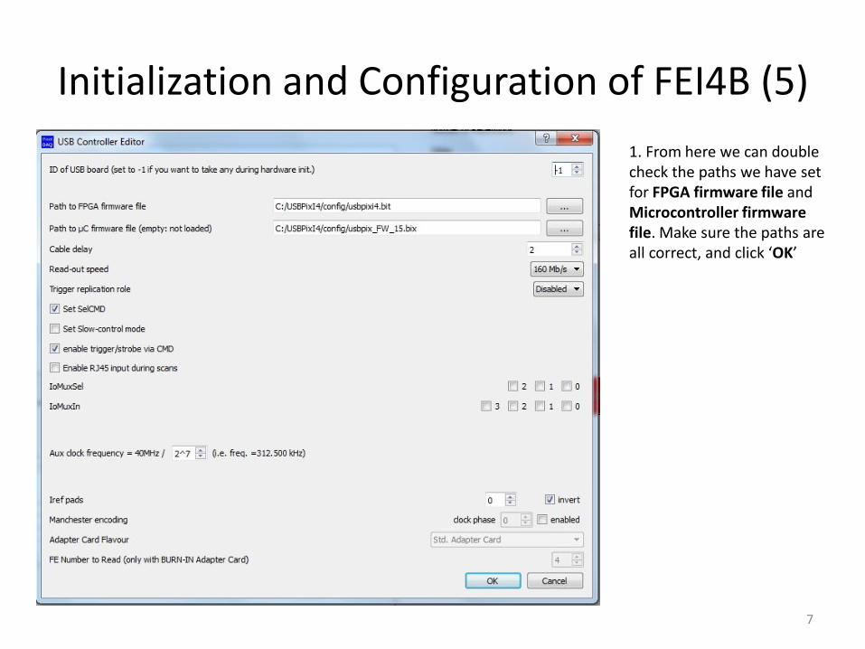
Initialization and Configuration of FEI4B (5)
1. From here we can double check the paths we have set for FPGA firmware file and Microcontroller firmware file. Make sure the paths are all correct, and click ‘OK’
7
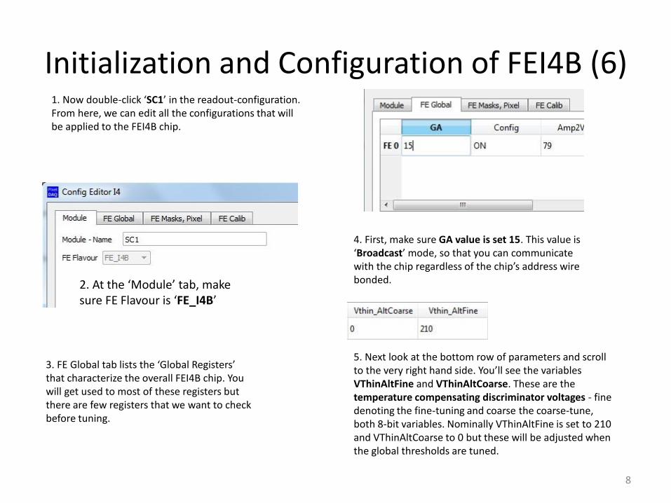
Initialization and Configuration of FEI4B (6) 1. Now double-click ‘SC1’ in the readout-configuration. From here, we can edit all the configurations that will be applied to the FEI4B chip.
2. At the ‘Module’ tab, make sure FE Flavour is ‘FE_I4B’
3. FE Global tab lists the ‘Global Registers’ that characterize the overall FEI4B chip. You will get used to most of these registers but there are few registers that we want to check before tuning.
4. First, make sure GA value is set 15. This value is ‘Broadcast’ mode, so that you can communicate with the chip regardless of the chip’s address wire bonded.
5. Next look at the bottom row of parameters and scroll to the very right hand side. You’ll see the variables VThinAltFine and VThinAltCoarse. These are the temperature compensating discriminator voltages - fine denoting the fine-tuning and coarse the coarse-tune, both 8-bit variables. Nominally VThinAltFine is set to 210 and VThinAltCoarse to 0 but these will be adjusted when the global thresholds are tuned.
8
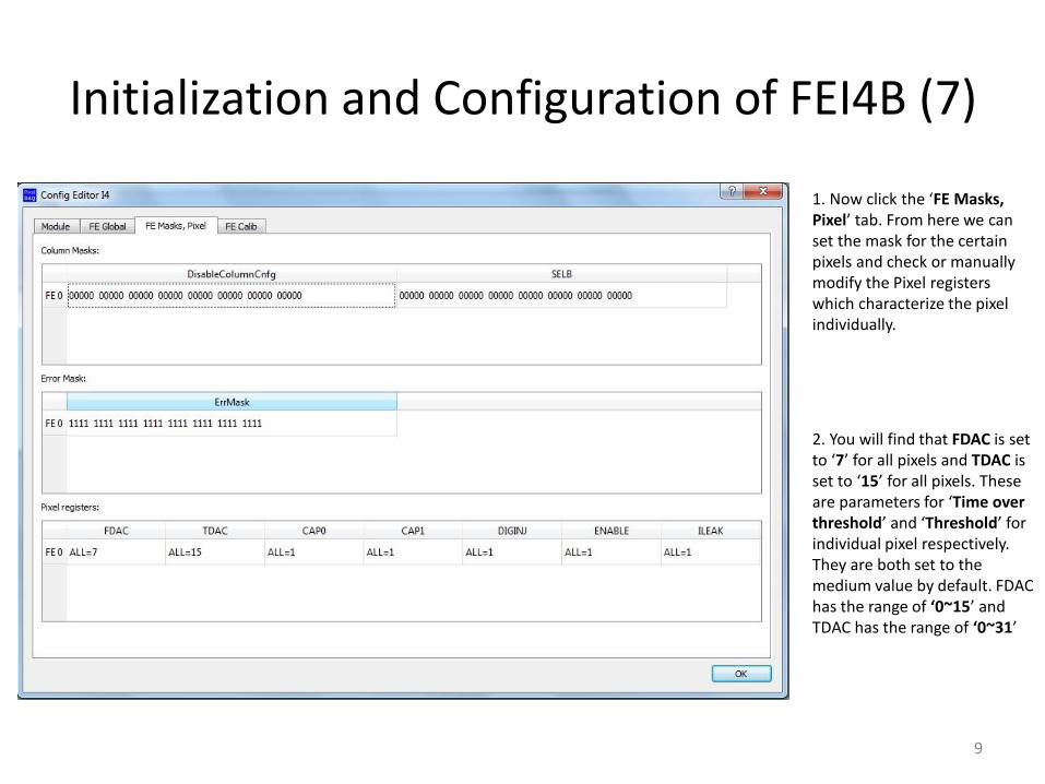
Initialization and Configuration of FEI4B (7)
1. Now click the ‘FE Masks, Pixel’ tab. From here we can set the mask for the certain pixels and check or manually modify the Pixel registers which characterize the pixel individually.
2. You will find that FDAC is set to ‘7’ for all pixels and TDAC is set to ‘15’ for all pixels. These are parameters for ‘Time over threshold’ and ‘Threshold’ for individual pixel respectively. They are both set to the medium value by default. FDAC has the range of ‘0~15’ and TDAC has the range of ‘0~31’
9
Initialization and Configuration of FEI4B (8)
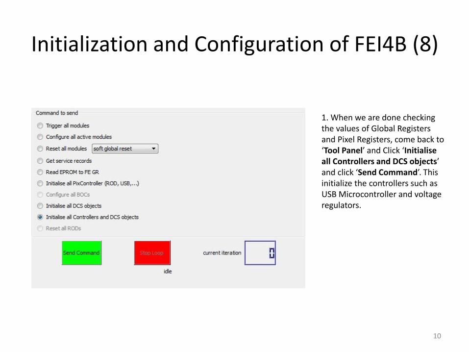
1. When we are done checking the values of Global Registers and Pixel Registers, come back to ‘Tool Panel’ and Click ‘Initialise all Controllers and DCS objects’ and click ‘Send Command’. This initialize the controllers such as USB Microcontroller and voltage regulators.
10
Initialization and Configuration of FEI4B (9)
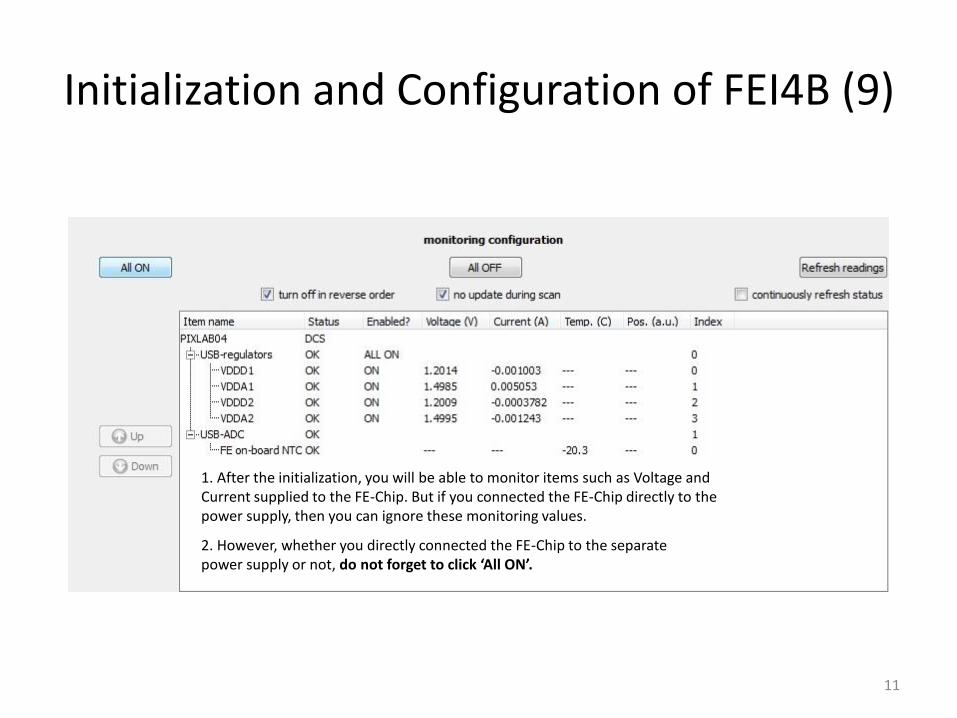
1. After the initialization, you will be able to monitor items such as Voltage and Current supplied to the FE-Chip. But if you connected the FE-Chip directly to the power supply, then you can ignore these monitoring values.
2. However, whether you directly connected the FE-Chip to the separate power supply or not, do not forget to click ‘All ON’.
11

Initialization and Configuration of FEI4B (10)
1. Once you click ‘All ON’ button, you will find out 4-Blue LED lights on the adapter card are now turned on and the current supplied to the adapter has increased to around 50mA and current supplied to the FEI4B card has increased to 300mA
12
Initialization and Configuration of FEI4B (11)
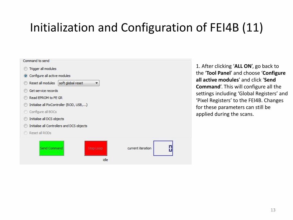
1. After clicking ‘ALL ON’, go back to the ‘Tool Panel’ and choose ‘Configure all active modules’ and click ‘Send Command’. This will configure all the settings including ‘Global Registers’ and ‘Pixel Registers’ to the FEI4B. Changes for these parameters can still be applied during the scans.
13
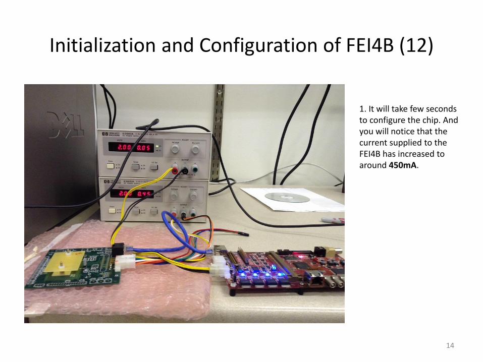
Initialization and Configuration of FEI4B (12)
1. It will take few seconds to configure the chip. And you will notice that the current supplied to the FEI4B has increased to around 450mA.
14
Basic Communication Scan; Digital and Analog Test (1)
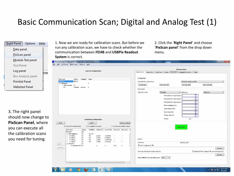
1. Now we are ready for calibration scans. But before we run any calibration scan, we have to check whether the communication between FEI4B and USBPix Readout System is correct.
2. Click the ‘Right Panel’ and choose ‘PixScan panel’ from the drop down menu.
3. The right panel should now change to PixScan Panel, where you can execute all the calibration scans you need for tuning.
15
Basic Communication Scan; Digital and Analog Test (2)
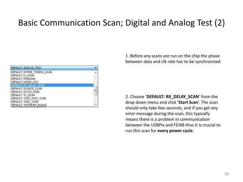
1. Before any scans are run on the chip the phase between data and clk rate has to be synchronized.
2. Choose ‘DEFAULT: RX_DELAY_SCAN’ from the drop down menu and click ‘Start Scan’. The scan should only take few seconds, and if you get any error message during the scan, this typically means there is a problem in communication between the USBPix and FEI4B thus it is crucial to run this scan for every power cycle.
16
Basic Communication Scan; Digital and Analog Test (3)
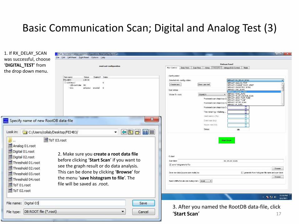
1. If RX_DELAY_SCAN was successful, choose ‘DIGITAL_TEST’ from the drop down menu.
2. Make sure you create a root data file before clicking ‘Start Scan’ if you want to see the graph result or do data analysis. This can be done by clicking ‘Browse’ for the menu ‘save histogram to file’. The file will be saved as .root.
3. After you named the RootDB data-file, click ‘Start Scan’ 17
Basic Communication Scan; Digital and Analog Test (4)
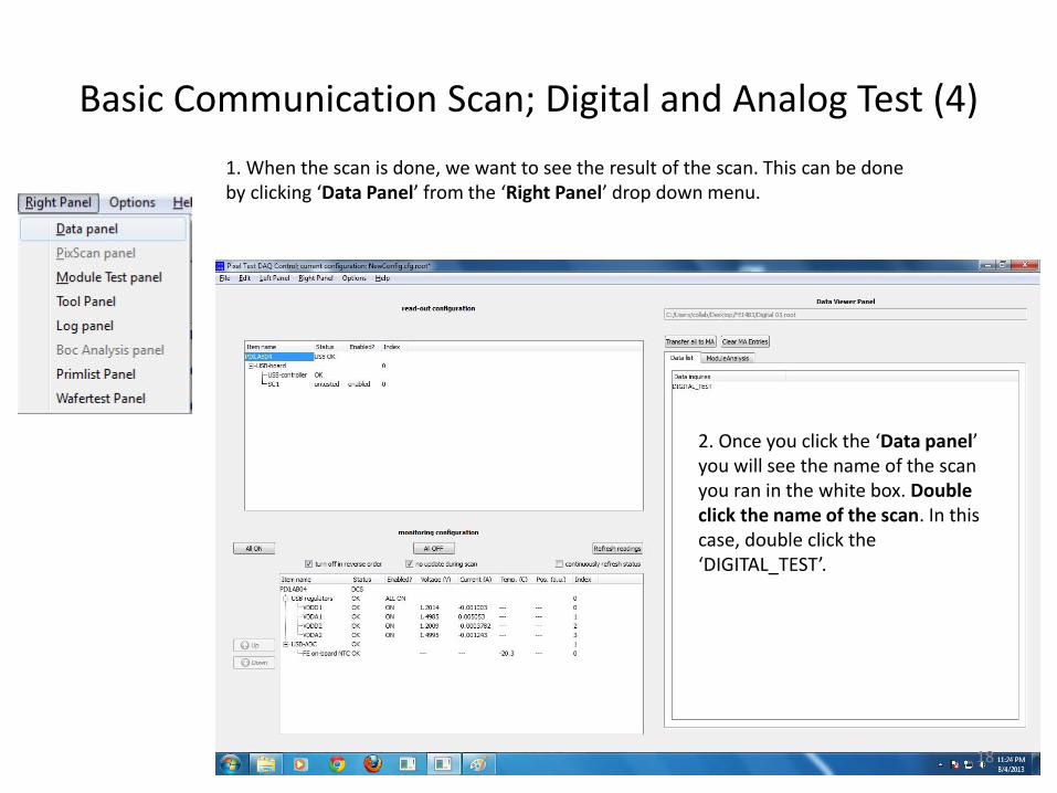
1. When the scan is done, we want to see the result of the scan. This can be done by clicking ‘Data Panel’ from the ‘Right Panel’ drop down menu.
2. Once you click the ‘Data panel’ you will see the name of the scan you ran in the white box. Double click the name of the scan. In this case, double click the ‘DIGITAL_TEST’.
18
Basic Communication Scan; Digital and Analog Test (5)
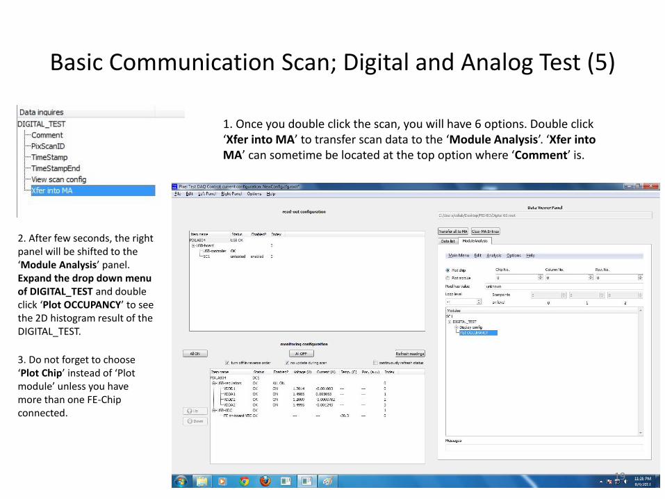
1. Once you double click the scan, you will have 6 options. Double click ‘Xfer into MA’ to transfer scan data to the ‘Module Analysis’. ‘Xfer into MA’ can sometime be located at the top option where ‘Comment’ is.
2. After few seconds, the right panel will be shifted to the ‘Module Analysis’ panel. Expand the drop down menu of DIGITAL_TEST and double click ‘Plot OCCUPANCY’ to see the 2D histogram result of the DIGITAL_TEST.
3. Do not forget to choose ‘Plot Chip’ instead of ‘Plot module’ unless you have more than one FE-Chip connected.
19
Basic Communication Scan; Digital and Analog Test (6)
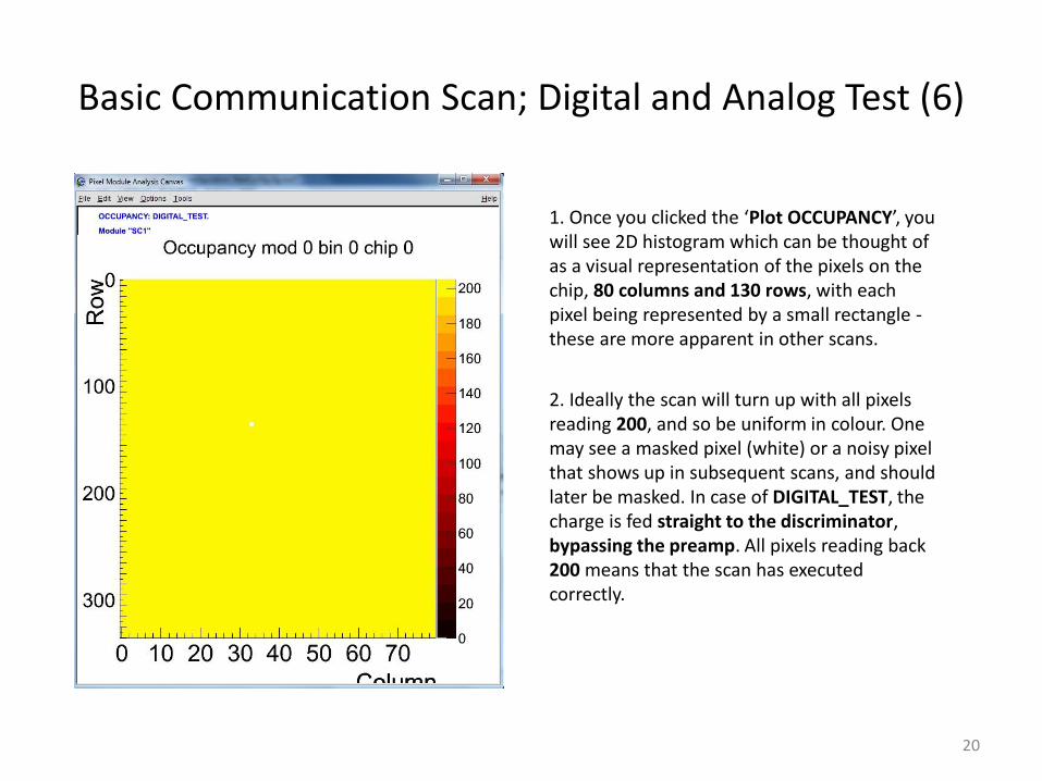
1. Once you clicked the ‘Plot OCCUPANCY’, you will see 2D histogram which can be thought of as a visual representation of the pixels on the chip, 80 columns and 130 rows, with each pixel being represented by a small rectangle - these are more apparent in other scans.
2. Ideally the scan will turn up with all pixels reading 200, and so be uniform in colour. One may see a masked pixel (white) or a noisy pixel that shows up in subsequent scans, and should later be masked. In case of DIGITAL_TEST, the charge is fed straight to the discriminator, bypassing the preamp. All pixels reading back 200 means that the scan has executed correctly.
20
Basic Communication Scan; Digital and Analog Test (6)
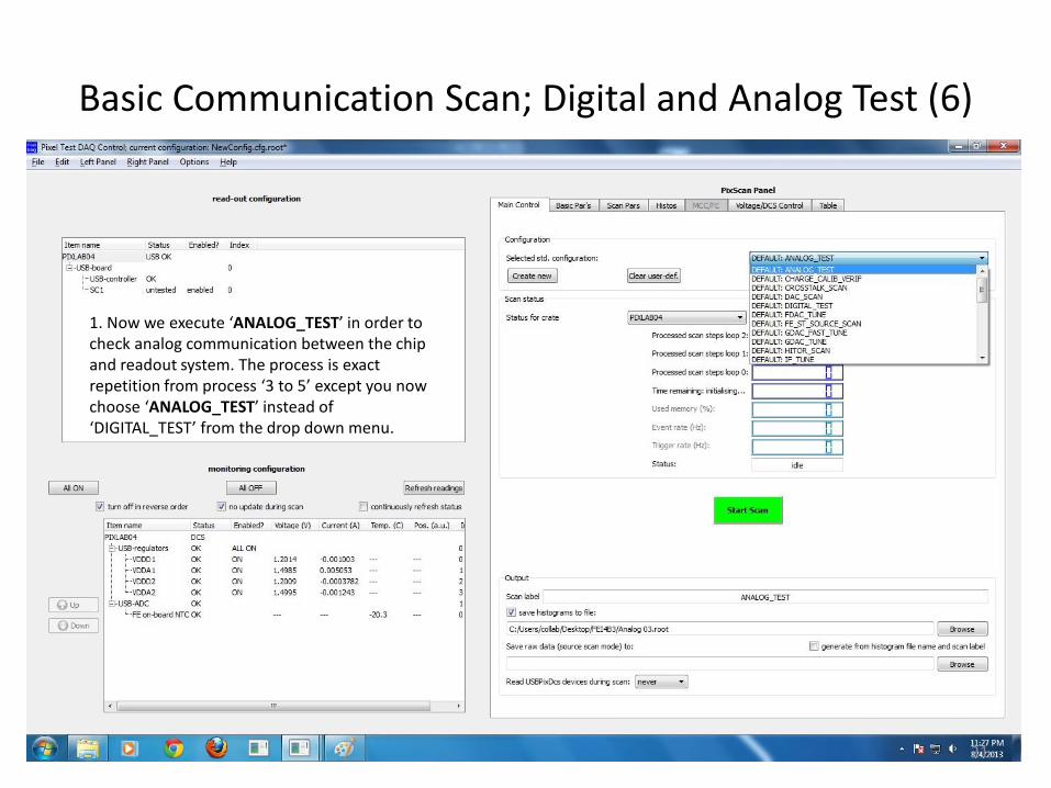
1. Now we execute ‘ANALOG_TEST’ in order to check analog communication between the chip and readout system. The process is exact repetition from process ‘3 to 5’ except you now choose ‘ANALOG_TEST’ instead of ‘DIGITAL_TEST’ from the drop down menu.
21
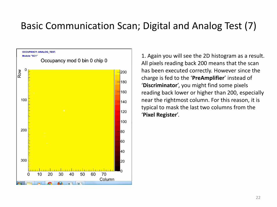
Basic Communication Scan; Digital and Analog Test (7)
1. Again you will see the 2D histogram as a result. All pixels reading back 200 means that the scan has been executed correctly. However since the charge is fed to the ‘PreAmplifier’ instead of ‘Discriminator’, you might find some pixels reading back lower or higher than 200, especially near the rightmost column. For this reason, it is typical to mask the last two columns from the ‘Pixel Register’.
22
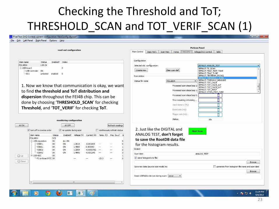
Checking the Threshold and ToT; THRESHOLD_SCAN and TOT_VERIF_SCAN (1)
1. Now we know that communication is okay, we want to find the threshold and ToT distribution and dispersion throughout the FEI4B chip. This can be done by choosing ‘THRESHOLD_SCAN’ for checking Threshold, and ‘TOT_VERIF’ for checking ToT.
2. Just like the DIGITAL and ANALOG TEST, don’t forget to save the RootDB data file for the histogram results.
23

Checking the Threshold and ToT; THRESHOLD_SCAN and TOT_VERIF_SCAN (2)
1. The left picture is the histograms you get when you choose ‘SCURVE_MEAN: THRESHOLD_SCAN’ from the MA. The right picture is the histograms you get when you choose ‘TOT_MEAN: TOT_VERIF’ from the MA. These three histograms show the distribution and dispersion of Threshold or ToT values throughout the chip but just in different methods. Top histogram is the one that is similar to the histogram we saw from the DIGITAL and ANALOG TEST. Each rectangle stands for a pixel and it is colored to the corresponding threshold value.
2. The middle histogram has X-Axis as the threshold or
ToT value and Y-Axis as the number of
pixels. Thus, it shows the distribution of
number of pixels for corresponding
threshold or ToT value. In the white box, ‘Constant’ is Y
value at the peak of the curve, ‘Mean’ is the mean value of
the threshold or ToT throughout the chip,
and ‘Sigma’ corresponds to the
dispersion calculated from the fit-curve.
3. The goal of the tuning is to tune these pixels so that they all have uniform value of Threshold and ToT value with desired target mean value (ex: Threshold: 3000e, ToT: 6, based on reference charge of 20000e). In order to do this, we need to decrease the dispersion value by tuning each pixel individually.
24
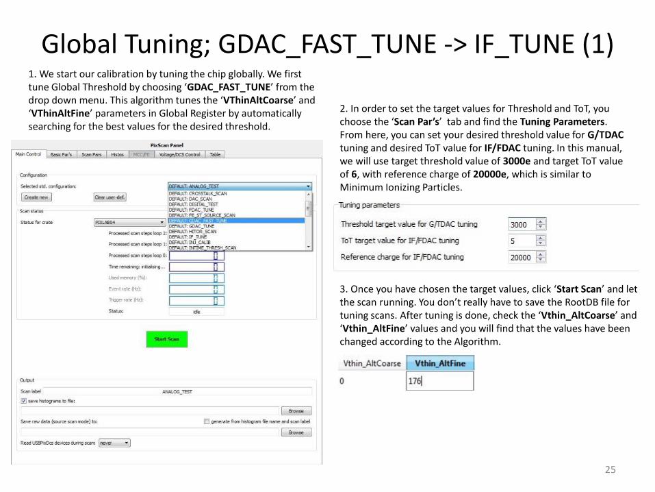
Global Tuning; GDAC_FAST_TUNE -> IF_TUNE (1) 1. We start our calibration by tuning the chip globally. We first
tune Global Threshold by choosing ‘GDAC_FAST_TUNE’ from the drop down menu. This algorithm tunes the ‘VThinAltCoarse’ and ‘VThinAltFine’ parameters in Global Register by automatically searching for the best values for the desired threshold.
2. In order to set the target values for Threshold and ToT, you choose the ‘Scan Par’s’ tab and find the Tuning Parameters. From here, you can set your desired threshold value for G/TDAC tuning and desired ToT value for IF/FDAC tuning. In this manual, we will use target threshold value of 3000e and target ToT value of 6, with reference charge of 20000e, which is similar to Minimum Ionizing Particles.
3. Once you have chosen the target values, click ‘Start Scan’ and let the scan running. You don’t really have to save the RootDB file for tuning scans. After tuning is done, check the ‘Vthin_AltCoarse’ and ‘Vthin_AltFine’ values and you will find that the values have been changed according to the Algorithm.
25
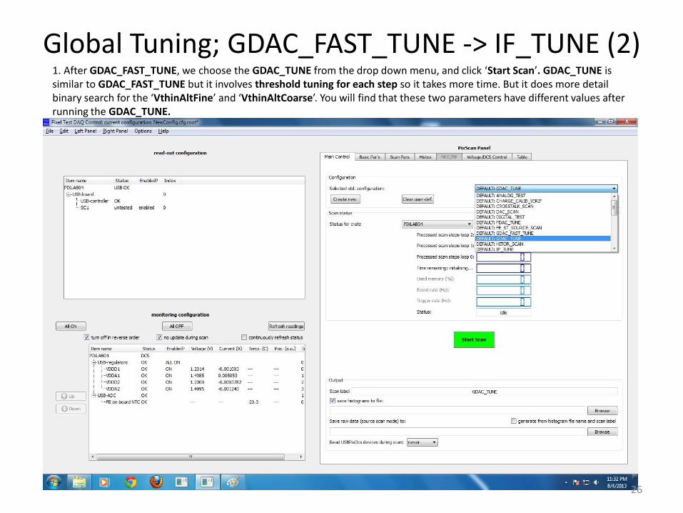
Global Tuning; GDAC_FAST_TUNE -> IF_TUNE (2)
1. After GDAC_FAST_TUNE, we choose the GDAC_TUNE from the drop down menu, and click ‘Start Scan’. GDAC_TUNE is similar to GDAC_FAST_TUNE but it involves threshold tuning for each step so it takes more time. But it does more detail binary search for the ‘VthinAltFine’ and ‘VthinAltCoarse’. You will find that these two parameters have different values after running the GDAC_TUNE.
26

Global Tuning; GDAC_FAST_TUNE -> IF_TUNE (3)
1. After GDAC_TUNE, we can now tune the global ToT value. This can be done by choosing ‘IF_TUNE’ from the drop down menu. Make sure you check the desired ToT value and reference charge from the Scan Pars tab and click ‘Start Scan’ button.
2. After tuning is done, you can find that ‘PrmpVbp’ value from the global register tab has been changed. This value serves similar purpose for global ToT value like ‘VthinAltFine’ and ‘VthinAltCoarse’ are for global threshold.
27
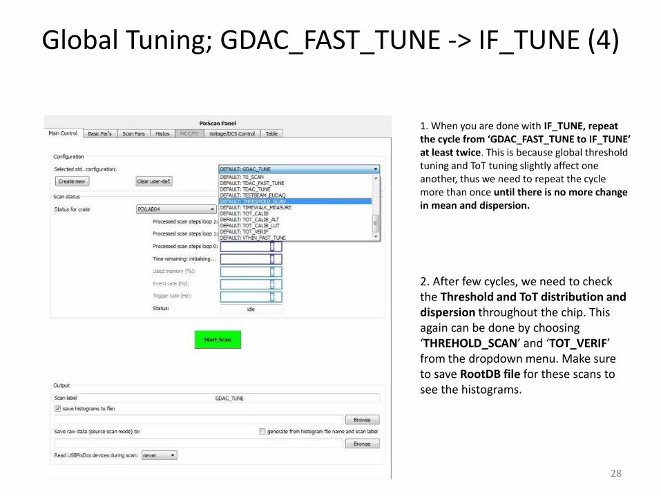
Global Tuning; GDAC_FAST_TUNE -> IF_TUNE (4)
1. When you are done with IF_TUNE, repeat the cycle from ‘GDAC_FAST_TUNE to IF_TUNE’ at least twice. This is because global threshold tuning and ToT tuning slightly affect one another, thus we need to repeat the cycle more than once until there is no more change in mean and dispersion.
2. After few cycles, we need to check the Threshold and ToT distribution and dispersion throughout the chip. This again can be done by choosing ‘THREHOLD_SCAN’ and ‘TOT_VERIF’ from the dropdown menu. Make sure to save RootDB file for these scans to see the histograms.
28
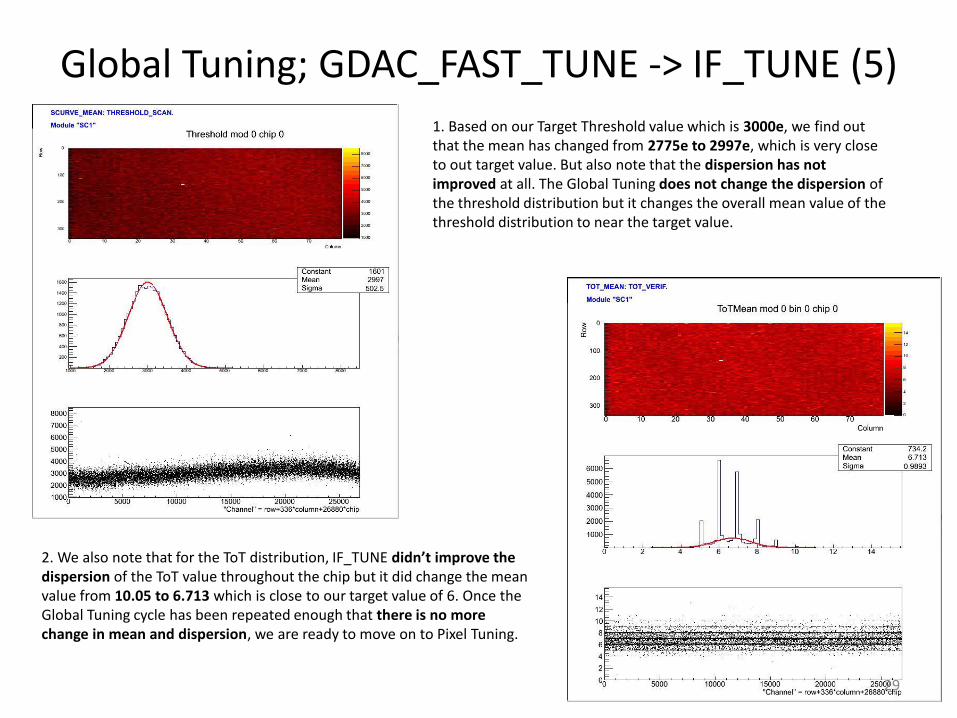
Global Tuning; GDAC_FAST_TUNE -> IF_TUNE (5) 1. Based on our Target Threshold value which is 3000e, we find out
that the mean has changed from 2775e to 2997e, which is very close to out target value. But also note that the dispersion has not improved at all. The Global Tuning does not change the dispersion of the threshold distribution but it changes the overall mean value of the threshold distribution to near the target value.
2. We also note that for the ToT distribution, IF_TUNE didn’t improve the dispersion of the ToT value throughout the chip but it did change the mean value from 10.05 to 6.713 which is close to our target value of 6. Once the Global Tuning cycle has been repeated enough that there is no more change in mean and dispersion, we are ready to move on to Pixel Tuning.
29
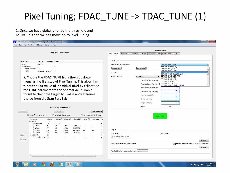
Pixel Tuning; FDAC_TUNE -> TDAC_TUNE (1) 1. Once we have globally tuned the threshold and
ToT value, then we can move on to Pixel Tuning.
2. Choose the FDAC_TUNE from the drop down menu as the first step of Pixel Tuning. This algorithm tunes the ToT value of individual pixel by calibrating the FDAC parameter to the optimal value. Don’t forget to check the target ToT value and reference charge from the Scan Pars Tab
30

Pixel Tuning; FDAC_TUNE -> TDAC_TUNE (2)
1. After tuning is done, you can check the Pixel Register tab and you can see that the FDAC parameter has changed from default value of 7 to ‘map’. This means that now all the pixels on the chip have different FDAC value, optimally chosen by the FDAC_TUNE algorithm
2. You can right click the ‘map’ and click ‘Display/Edit’ then you will see the colored array of FDAC value throughout the chip. Again, each rectangle corresponds to individual pixel. From this ‘Config Map’ you can manually change the value of each individual pixel or mask the certain row or column.
31
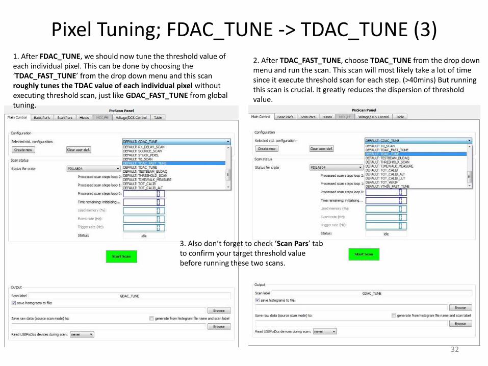
Pixel Tuning; FDAC_TUNE -> TDAC_TUNE (3)
1. After FDAC_TUNE, we should now tune the threshold value of each individual pixel. This can be done by choosing the ‘TDAC_FAST_TUNE’ from the drop down menu and this scan roughly tunes the TDAC value of each individual pixel without executing threshold scan, just like GDAC_FAST_TUNE from global tuning.
2. After TDAC_FAST_TUNE, choose TDAC_TUNE from the drop down menu and run the scan. This scan will most likely take a lot of time since it execute threshold scan for each step. (>40mins) But running this scan is crucial. It greatly reduces the dispersion of threshold value.
32
3. Also don’t forget to check ‘Scan Pars’ tab to confirm your target threshold value before running these two scans.
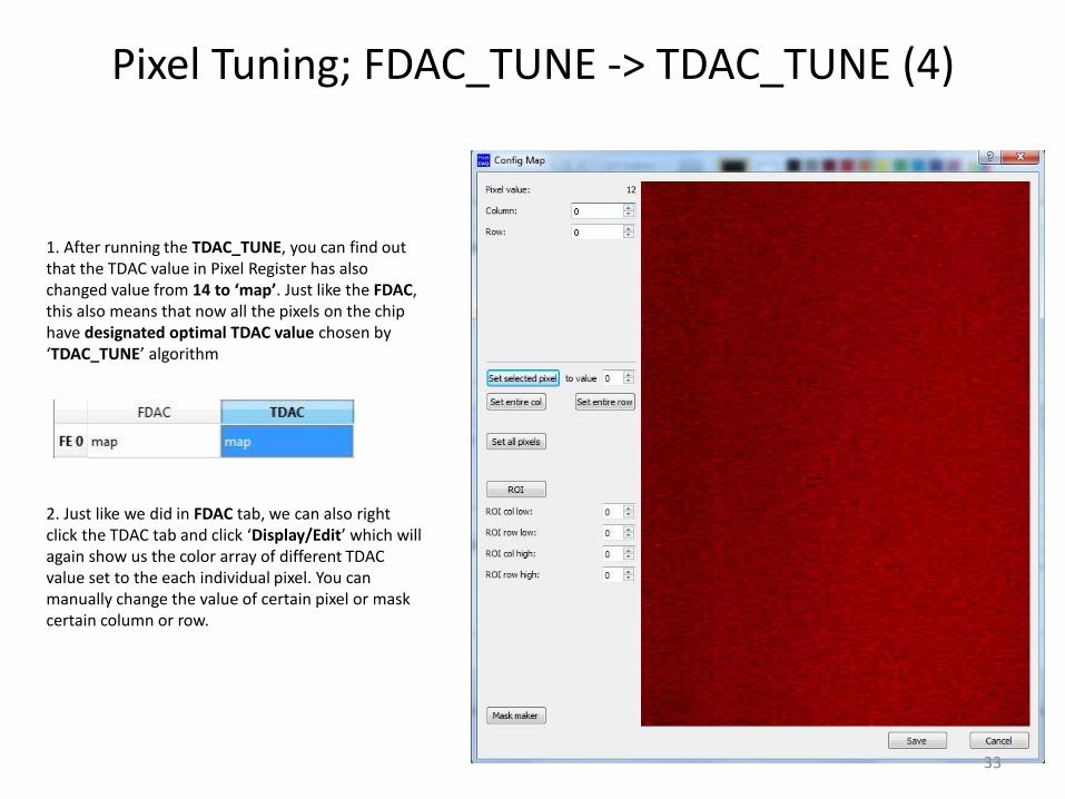
Pixel Tuning; FDAC_TUNE -> TDAC_TUNE (4)
1. After running the TDAC_TUNE, you can find out that the TDAC value in Pixel Register has also changed value from 14 to ‘map’. Just like the FDAC, this also means that now all the pixels on the chip have designated optimal TDAC value chosen by ‘TDAC_TUNE’ algorithm
2. Just like we did in FDAC tab, we can also right click the TDAC tab and click ‘Display/Edit’ which will again show us the color array of different TDAC value set to the each individual pixel. You can manually change the value of certain pixel or mask certain column or row.
33
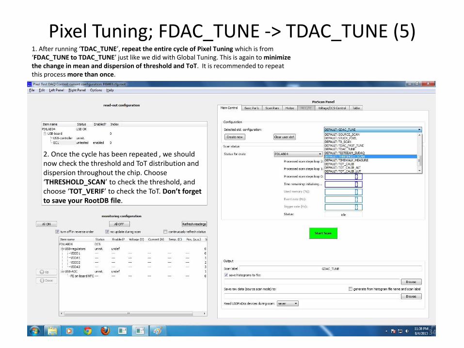
Pixel Tuning; FDAC_TUNE -> TDAC_TUNE (5)
1. After running ‘TDAC_TUNE’, repeat the entire cycle of Pixel Tuning which is from ‘FDAC_TUNE to TDAC_TUNE’ just like we did with Global Tuning. This is again to minimize the change in mean and dispersion of threshold and ToT. It is recommended to repeat this process more than once.
2. Once the cycle has been repeated , we should now check the threshold and ToT distribution and dispersion throughout the chip. Choose ‘THRESHOLD_SCAN’ to check the threshold, and choose ‘TOT_VERIF’ to check the ToT. Don’t forget to save your RootDB file.
34
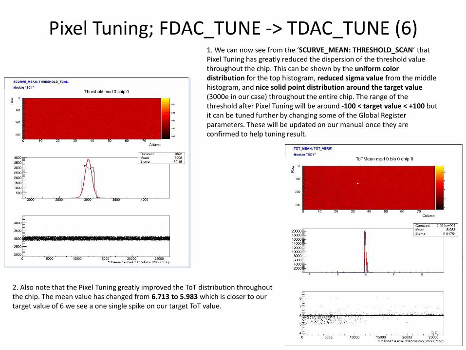
Pixel Tuning; FDAC_TUNE -> TDAC_TUNE (6)
1. We can now see from the ‘SCURVE_MEAN: THRESHOLD_SCAN’ that Pixel Tuning has greatly reduced the dispersion of the threshold value throughout the chip. This can be shown by the uniform color distribution for the top histogram, reduced sigma value from the middle histogram, and nice solid point distribution around the target value (3000e in our case) throughout the entire chip. The range of the threshold after Pixel Tuning will be around -100 < target value < +100 but it can be tuned further by changing some of the Global Register parameters. These will be updated on our manual once they are confirmed to help tuning result.
2. Also note that the Pixel Tuning greatly improved the ToT distribution throughout the chip. The mean value has changed from 6.713 to 5.983 which is closer to our target value of 6 we see a one single spike on our target ToT value.
35
Related Documents