MAINTENANCE MANUAL 406-512 MHz EXCITER BOARD 19Ihi32679(31,2,3, ‘7 TABLE OF CONTENTS m DESCRIPTION ... .........*..................................................................................................*............. 1 CIRCUIT ANALYSIS ................... .............*...................*................................................................ 1 OUTLINE DIAGRAM ......... ......................*................................................................................... 5 SCHEMATIC DIAGRAM ......................................................................... ........ ..................: ..... ...... .58,9 MODIFICATION INSTRUCTIONS (VOICE GUARD) ........................................................ .... . 6 PARTS LIST AND PRODUCTION CHANGES .................................. ................................**...*... 10 DESCRIPTION The exciter uses seven transistors and an integrated circuit to provide 185 milliwatts of RF drive to the PA assembly. The exciter can be equipped with up to eight Inte- grated Circuit Oscillator Modules FM (ICOMs). The FM ICOM crystal frequency ranges from approximately 11.3 to 14.2 megahertz, and the crystal frequency is multi- plied 36 times. Audio, supply voltages and control functions are connected from the system board to the exciter board through P902. Centralized metering jack JlOS is provided for use with GE Test Set Model 4EX3All or Test Kit 4EX8K12. The test set meters the modulator, multiplier and ampli- fier stages, and the regulated lo-volts. CIRCUIT ANALYSIS FM ICOMS (Frequency Modulated) Three different types of FM ICOMs are available for The FM ICOMs have an audio input which receives use in the exciter. Each ICOM contains a crystalOcon- audio from the audio processor circuit. Therefore, with trolled Colpius oscillator, and two of the ICOMs contain Modulation present, the output frequency of the “FM” compensator ICs. The different FM 1COM.s are: ICOM varies at an audio rate. 5GFM ICOM - contains an oscillator and a 5 parts-per-million (*O.OOOS%) compensator IC. Provides com- pensation for EC-ICOMs. EC-FM ICOM - contains an oscillator only, Re- quires external compensation from a 5GICOM. 2GFM ICOM - contains an oscillator and a 2 PPM (*0.0002%) compensator IC. Will not provide compensa- tion for an EGFM ICOM. The ICOMs are enclosed in a RF shielded can with the type ICOM (BGFM ICOM, EGFM ICOM or PGFM ICOM) printed on the top of the can. Access to the oscillator trimmer is obtained through a hole in the top of the can. Frequency selection is accomplished by switching the ICOM keying lead (terminal 9) to A- by means of the frequency selector switch on the control unit. In single- frequency radios, a jumper from H9 to HlO in the con- trol unit connects terminal 9 of the FM ICOM to A-. The oscillator is turned on by applying a keyed t10 Volts to the external oscillator collector load resistor (R111) which forward biases an internal diode switch. 1

Welcome message from author
This document is posted to help you gain knowledge. Please leave a comment to let me know what you think about it! Share it to your friends and learn new things together.
Transcript
MAINTENANCE MANUAL
406-512 MHz EXCITER BOARD 19Ihi32679(31,2,3, ‘7
TABLE OF CONTENTS
m DESCRIPTION . . . . . . . . . . ..*..................................................................................................*............. 1
CIRCUIT ANALYSIS . . . . . . . . . . . . . . . . . . . . . . . . . . . . . . ..*...................*................................................................ 1
OUTLINE DIAGRAM . . . . . . . . . . . . . . . . . . . . . . . . . . . . . ..*................................................................................... 5
SCHEMATIC DIAGRAM . . . . . . . . . . . . . . . . . . . . . . . . . . . . . . . . . . . . . . . . . . . . . . . . . . . . . . . . . . . . . . . . . . . . . . . . . . . . . . . . . . . . . . . . . . . . . . . . . . . : . . . . . . . . . . . .58,9 MODIFICATION INSTRUCTIONS (VOICE GUARD) . . . . . . . . . . . . . . . . . . . . . . . . . . . . . . . . . . . . . . . . . . . . . . . . . . . . . . . . . . . . . 6
PARTS LIST AND PRODUCTION CHANGES . . . . . . . . . . . . . . . . . . . . . . . . . . . . . . . . . . . . . . . . . . . . . . . . . . . . . . . . . . . . . . . . ..**...*... 10
DESCRIPTION
The exciter uses seven transistors and an integrated circuit to provide 185 milliwatts of RF drive to the PA assembly.
The exciter can be equipped with up to eight Inte- grated Circuit Oscillator Modules FM (ICOMs). The FM ICOM crystal frequency ranges from approximately 11.3 to 14.2 megahertz, and the crystal frequency is multi- plied 36 times.
Audio, supply voltages and control functions are connected from the system board to the exciter board through P902.
Centralized metering jack JlOS is provided for use with GE Test Set Model 4EX3All or Test Kit 4EX8K12. The test set meters the modulator, multiplier and ampli- fier stages, and the regulated lo-volts.
CIRCUIT ANALYSIS
FM ICOMS (Frequency Modulated)
Three different types of FM ICOMs are available for The FM ICOMs have an audio input which receives use in the exciter. Each ICOM contains a crystalOcon- audio from the audio processor circuit. Therefore, with trolled Colpius oscillator, and two of the ICOMs contain Modulation present, the output frequency of the “FM” compensator ICs. The different FM 1COM.s are: ICOM varies at an audio rate.
5GFM ICOM - contains an oscillator and a 5 parts-per-million (*O.OOOS%) compensator IC. Provides com- pensation for EC-ICOMs.
EC-FM ICOM - contains an oscillator only, Re- quires external compensation from a 5GICOM.
2GFM ICOM - contains an oscillator and a 2 PPM (*0.0002%) compensator IC. Will not provide compensa- tion for an EGFM ICOM.
The ICOMs are enclosed in a RF shielded can with the type ICOM (BGFM ICOM, EGFM ICOM or PGFM ICOM) printed on the top of the can. Access to the oscillator trimmer is obtained through a hole in the top of the can.
Frequency selection is accomplished by switching the ICOM keying lead (terminal 9) to A- by means of the frequency selector switch on the control unit. In single- frequency radios, a jumper from H9 to HlO in the con- trol unit connects terminal 9 of the FM ICOM to A-. The oscillator is turned on by applying a keyed t10 Volts to the external oscillator collector load resistor (R111) which forward biases an internal diode switch.
1

- _._.I .__ 1 _-_ -.-,.- _.__. -- --.-_ -.. a- A.- .w..
LB/-31209
r All ICOMs are individually compensated at the factory and cannot be repaired in the field. Any attempt to repair or change the ICOM fre- quency will void the warranty.
In standard 5 PPM radios using EGFM ICOMs, at least one 5GFM ICOM or 5C ICOM must be used. The 5C ICOM is normally used in the receiver Fl position. A 5GFM ICOM can be used in any transmit position.
NOTE
The EC and 5C type ICOMs are not interchange- able with EGFM or 5C FM type ICOMs. The EC and 5C type ICOMs are used only in the receiv- ers. While the EGFM and 5GFM type ICOMs are always used in the transmitter.
Figure 1 shows the typical performance of an uncom- pensated crystal as well as the typical performance of a crystal which has been matched with a properly chosen 0 compensation capacitor.
TYPICAL UNCBhWNSATEO
I I -10 t \ ,
I -15. +10- 26.5. +42* 65.
DEGREES CENTIGRADE
Figure 1 - Typical Crystal Characteristics
One 5C ICOM or 5GFM ICOM can be provide compensation for up to 15 EC ICOMs or EGFM ICOMs in the transmitter and receiver. Should the 5C ICOM or the 5GFM ICOM compensator fail in the open mode, the EGFM ICOMs will still maintain 2 PPM frequency stability from O’C to 55-C (+32-F to 1Sl’F) due to the regulated compensation voltage (5 Volts) from the 10 Volt regulator IC. If desired, up to 8 5GFM ICOMs may be used in the radio.
The PC-FM ICOMs are self-compensated at 2 PPM and will not provide compensation for EGFM ICOMs.
Oscillator Circuit
Quartz crystals used in ICOMs exhibit the traditional “S” curve characteristics of output frequency versus op erating temperature.
At both the coldest and hottest temperatures, the frequency increases with increasing temperature. In the middle temperature range (approximately O’C to 55%)) frequency decreases with increasing temperature.
Since the rate of change is nearly linear over the mid-temperature range, the output frequency change can be compensated by choosing a parallel compensa- don capacitor with a temperature coeficient approxi- mately equal to and opposite that of the crystal.
At temperatures above and below the mid-range, additional compensation must be introduced. An exter- nally generated compensation voltage is applied to a varactor (voltage-variable capacitor) connected in paral- lel with the crystal. Refer to Figure 2 for a simplified diagram of the FM ICOM. 0
A constant bias of 5 Volts (provided from Regulator IC U901 connected in parallel with the compensator) maintains varactor capacity at a constant value over the entire mid-temperature range. This compensation volt- age achieves the t2 PPM stability.
Modulation is accomplished with a hyperabrupt vari- cap connected in series with the crystal feedback capac- itors. The varicap impedance is the dominant impedance in the loop. This allows large swings of load capacity with modulation, therefore, large frequency shifts are achieved for the modulated input. Biasing for the modulation varicap is provided by a voltage divider, R112 and R113, connected across the 10 volt regulator input at P902-7. A bias voltage of 6.2 volts is applied to pin 6 of all ICOMs.
Compensator Circuits
Both the 5GICOMs and PGFM ICOMs are temper- ature compensated at both ends of the temperature range to provide instant frequency compensation.
The cold end compensation circuit does not operate at temperatures above 0%. When the temperature drops 0 below O’C, the circuit is activated. As the temperature
2

n
ar
decreases, the equivalent resistance decreases and the compensation voltage increases.
An increase in compensation voltage decreases the capacitance of the varactor in the oscillator, thereby increasing the output frequency of the ICOM.
The hot end compensation circuit does not operate at temperatures below +55”C. When the temperature rises above +55X, the circuit is activated. As the temper- ature increases, the equivalent resistance decreases and the compensation voltage decreases. The decrease in compensation voltage increases the capacity of the varac- tor, decreasing the output frequency of the ICOM.
Proper ICOM operation is dependent on the
r~SERWCENOTE ----,
closely-controlled input voltages for the lo-Volt regulator. Should all of the ICOMs shift off fre- quency, check the lo-Volt regulator module.
AUDIO PROCESSOR A101
The transmitter audio processor contains audio cir- cuitry consisting of two operational amplifiers, ARlOl-A
and -B, a pre-emphasis circuit with amplitude limiting and a post limiter ftiter. A total gain of approximately 24 dB is realized through the audio processor. Twenty dB is provided by ARlOl-B and 4 dB by ARlOl-A.
The 10 Volt regulator powers the audio processor and applies regulated t10 V thru P902-6 to a voltage divider consisting of R108 and RllO. The t5 V output from the voltage divider establishes the operating refer- ence point for both operational amplifiers. Cl07 filters out any noise that may be on the 10 Volt line to assure a stable voltage supply to the operational amplifiers.
Resistors R105, R106 and R107 and diodes CR101 and CR102 provide limiting for ARlOl-B. Diodes CR101 and CR102 are reverse biased by t5 VDC on ARlOlB-6 and voltage divider network R105, R106 and R107. The voltage divider network provides t7 VDC at the cathode of CR101 and +3 VDC at the anode of CR102. Cl02 and Cl03 permit a DC level change between ARlOlB-7 and the voltage divider network for diode biasing.
When the input signal to ARlOlB-6 is of amagnitude such that the amplifier output at ARlOlB-7 does not exceed 4 volts p-p, the amplifier provides a nominal 20 dB gain. When the audio signal level at ARlOlB-7 ex- ceeds 4 volts PP, diodes CR101 and CR102 conduct on the positive and negative half cycles providing 100% negative feedback to reduce the amplifier ain to 1. This limits the audio amplitude at ARlOlB-7 to 5 volts PP.
..* -
- ------- --- -
t - _^... .-_- I + IO” i I-J-l i
Figure 2 - Equivalent FM-ICOM Circuit
8 CopydghtC 1983. Genenl Electric Company
LBI-31209
Resistors, R102, RlO3 and R104 and Cl04 comprise the audio pre-emphasis network that enhances the signal to noise ratio. R104 and Cl04 control the preemphasis curve below limiting. R103 and Cl04 control the cut-off point for high frequency pm-emphasis. As high frequen- cies are attenuated, the gain of AR101 is increased.
25’C to 7O”C, maintains a constant modulation index over the normal operating temperature range. The re- sistance of RTlO1 increases with a decrease in tempera- 0
ture below 25’C, thereby decreasing the signal drive to audio amplifier QlOl.
Audio from the microphone is applied to the audio processor at P102-1 and coupled to the input of opera- tional amplifier ARlOl-B through RlOl and ClOl.
The amplified output of ARlOl-B is coupled through P102-4 audio MOD ADJ control R104, R102-3, C106, R112 and R113 to a second operational amplifier AR101A. Audio MOD ADJ control is set for a deviation of 4.5 kHz.
Audio amplifier QlOl has a nominal gain of 2. The temperature compensated audio is coupled through Cl14 to pin 3 of the FM ICOM. A varactor withing the FM ICOM is used to modulate the carrier frequency at the audio rate. The output of the FM ICOM is taken from pin 2 and applied to a buffer stage.
BUFFER, MULTIPLIERS & AMPLIFIER ‘e
The Channel Guard tone input is applied to the audio processor through P902-2, CG MOD ADJ R10.3 to P102-5. The CG tone is then coupled through Cl05 and Rlll to ARlOlA-2 where it is combined with the micro- phone audio. ARlOl-A provides a signal gain of approx- imately 4 dB.
A post limiter filter consisting of ARlOlA, R112- R114, Cl08 and Cl09 provide 12 dB per octave roll off. R109 and Cl 11 provide an additonai 6 dB per octave roll offforatotalof18dB.
I-- SERWE+ p,
R112-R114 are 1% resistors This tolerance must be maintained to assure proper operation of the post limiter filter. Use exact replacements.
Buffer Q102 is saturated when no RF signal is pres- ent. Applying an RF Signal to Q102 provides a sawtooth waveform at its collector to drive class C tripler, QlO3. The first tripler stage is metered through R117. The output of Q103 is coupled through tuned circuits T102,
mT103 and T104 to the base of the second tripler, Q104. T102, T103 and T104 are tuned to three times the crystal frequency. The second tripler stage, Q104 is metered through R122.
The output of 4104 is coupled through tuned cir- cuits T105 and T106 to the base of first doubler QlO5. T105 and T106 are tuned to nine times the crystal fre- quency. QlO5 is metered through R126. 0
The output of QlO5 is coupled through two tuned circuits (T107 and T108) to the base of second doubler Q106. These circuits are tuned to 18 times the crystal frequency (oneohalf the transmitter operating fre- quency) . QlOS is metered through R133.
The output of the post limiter filter is coupled throut RTlOl and R106 to the temperature compensated audio amplifier QlOl. -
- _
AUDIO AMPLIFIER
The output of Q106 is coupled to the base of power amplifier Q107 through impedance matching networks composed of C152, C155, L105, C156, C157, L106 and C161. These networks are all tuned to the operating frequency and present a high shunt impedance at the operating frequency. All other frequencies are shunted to ground. 4107 is metered through R142.
The output of the audio processor is applied to Impedance matching network Cl66, C157, L108, audio amplifier QlOl through temperature compensa- tor and biasing network consisting of RTlOl, R106 and
L113, C171, L109 and Cl75 matches the output of Q107 to the input of the PA Assembly. C167, C171, and Cl75
R109. RTlOl, with a nominal resistance of 50 ohms from are tuned to the proper operating frequency.
c
Ericsson GE Mobile Communications Inc. Mountain View Road*Lynchburg, Virginia 24502 Printed inU.S.A. 0
4 %
. ---- --~.“ll---l---l- -.y~L.--~_--~-_---_ I._._ .- - . -
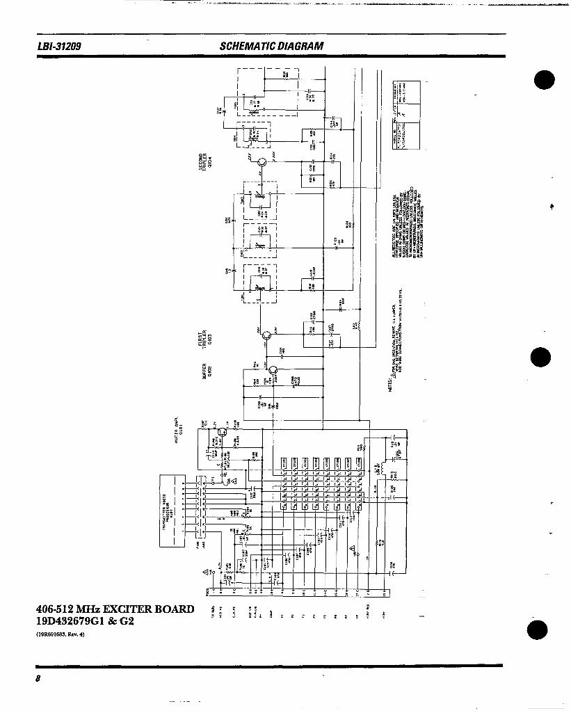
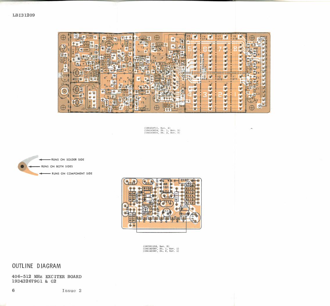
OUTLINE & SCHEMATIC DIAGRAMS LB/-31209
.
----A
(190331136, Rev. 3) (19*143587, Sh. 1, Rev. 1) (19A143587, Sh. 2, Rev. 1)
RUNS ON SOLDER SIDE
RUNS ON BOTH SIDES
RUNS ON COMPONENT SIDE
(19C321854, Rev. 9)
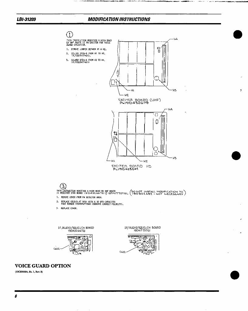
LBI-31299 MODIFICATION INSTRUCTIONS
:+iS :YSR”LJION nODIFIES A HIGH BAND Gil WF ?.BST? II FN EXCITER FOR VOICE d&T&l OPEUTION.
1. F=L)'E JWER BNN Hl L HZ.
2. XCii SF'&-R FROH Hl TO H3. :'LTi323C77461).
3. SCLDER SFZQ-R FRON HZ TO H4. :?Ll5%234774GlI I-L ---
i
iii HI
Q 3 THIS INSTRUCTION MODIFIES A HIGH BAND OR UHF MASTR II RECEIVER IF,% BOARD \3D43Zd(b?GI (1404\71076\.
INSTALL MODIFlCATlON TO \4~302432 -NOT NECE55AR-f
1. REMOVE COVER FROM FM DETECTOR AREA.
2. REPLACE CG22CO.47 UFO) WITH A 10 UFD CAPACITOR PART NUMBER 315A6047P106H (OBSERVE CORRECT POLARITY).
3. REPLACE COVER.
IF/AUD10/5QUELCH BOARD 190432667GJ
IF/AUDIO/SQUELCH BOARD 19D417707cJI
C622
c
VOICE GUARD OPTION (19CSS6664.Sh.l.Rcv. P)
6

VIEW AT-A' NUUBERIN,G FROU
WIRING END FOR P-t ANDP8
,---- - ---’
I + ;
+20 $I5 t5 I
f t’s +‘O
44 +4 litl* il.1 I
/ I -.;:
1
tl +‘2 p I
+I7 2 +” 4.2 I
1 /+I/ t’s ‘---- - --4’
VIEW AT% VIEW FROM WIRING END
OF 5933
-J @
CHANNEL GUARD PL19C331044GI PLlSC331462GI
HARNESS ~PLlSC320'311
J933
” ” -A
0 2 ,IS ,“S,“UC,,OXS C&CR THE l”STNJNlO” OF CA0I.E HIlllESS PLl%SSl,1419 62 I63 P‘3Ql3 1. IlSTN.L 01 .ulPEa LiE7Kf” HI * “8 0” CG E”omt. IF “I “LIT
PRESE”, COT lEn”Iul FRon “RBL “ME ( PL1923417W~ MO SOLMX TO “3. cOP.“~C, ODE” EHO TO J931-1‘ A”0 SPOT TIE TO EXISTING CtMHllEL MD IKWSS. SW IO SW 3 IF IIt IS llO1 PRESESI. *00lSkPa-\38?.347-w68
2. IF H, IS PIEPIT. ,“S,M,L YRSL “ME ,PL,9B23,77~GS7 II PI-2 L fCU&O”” E”0 VI J933-,a f SF31 TIE 70 EXISTIHG CHMWEL GOASP
1. UsTAlL ELLW YIP II FJOI-2 L GOLOU OniER E”0 TO J933-19.
2. 7IIs7ALL w-o YIlE I” PHII-IS MO SOLOER OTHER Em TO Jsss-20. spar TIE ELLaf Am OMSGE Y,W TO MIS7I”G Em* w!“Ess.
J. IRSWL YELLLY “IKE ~PLw92RP7PGI~ 7x P90,-2 S SOLDfX OIIIU F.Ki IO J933-19 I POT TIE 10 USTIHE EYQIES WISS. 3. REMOM 0.4 WIREB~WEEN J933-4 ,l.~t, ,~9-3?.-8.
4. IHST~U 0183.6~ 971~ (~~1sm77421 II ~901-78 L SOLDEI onm END ‘IO J9U-20‘ SPOT TIE TO fXISTlR6 UcllES IURXEI.
g. ,“GTNL OIhxE Y,tE PAR, OP PL,%xSlwm WR”fSS 11 PS-9 SOLW 0 6 a00 MHZ PST OTHER ~“0 To Ps-XL ,“STlLL MLLhl YIRE PP, OF PLlSCSS141~G2
1. 00 STEP 3 B 4 OFPARTZ.
“,S”ESS,X PF2 S SOLLZR 07HEll EHO 70 Pa-IS. IUSML XRSL YiSf p&x 0~ ~L,~us,,w~z IMHESS 7” P%-9 I SOLDEX THE OWES Eli0 70
2. 00 STERSlTHR”3 OFPART,.
PI-V. SW7 TIE TIE PL,~SS,‘,‘UiZ “WF.S-9 TO EXlS7MG 3. ON HARNESS 19C320811G15 O~CGX~,‘B~OVS HIRES. mm4
PLlW208lI umfS.9. Pa-8.9.1oau. CUT W~ESAND TIE BACK IN HARNESS.
406~512MHzEXCITERBOARD ; ; ; ;!I 5 ~ : ” f 19D432679618c G2 ” : t I P : f .
(19IcE.91695, Rev. 4)
8
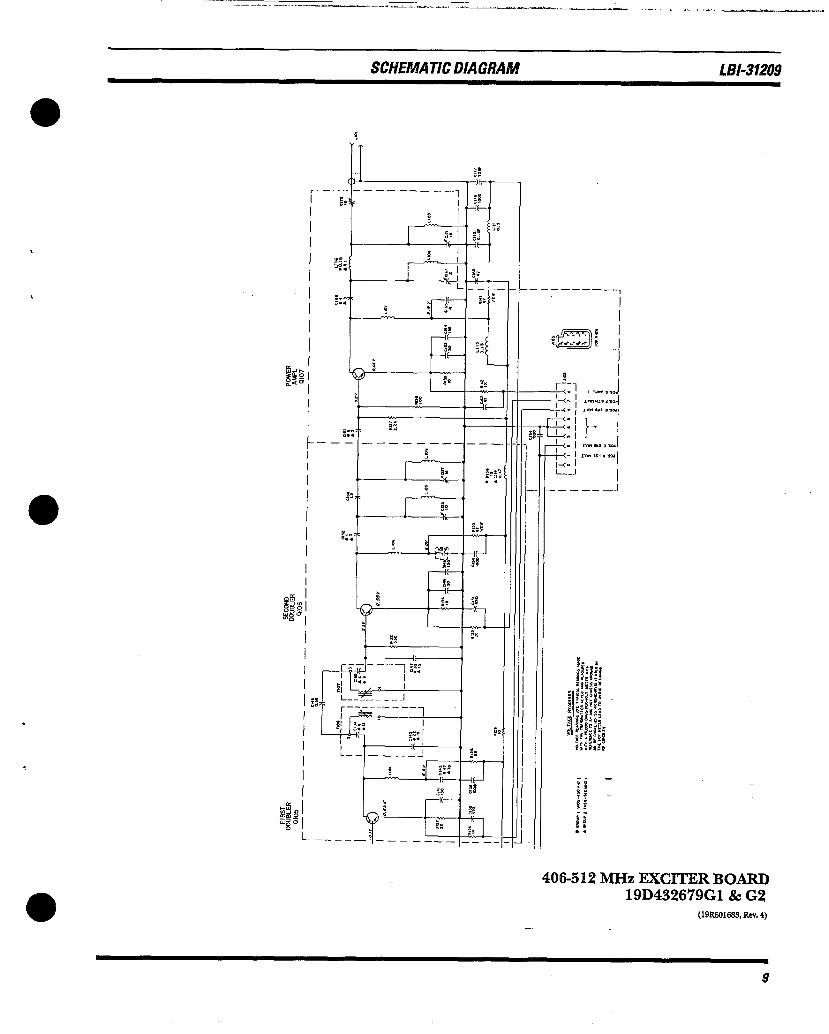
SCHEMATIC DIAGRAM LBI-31209
L-J -I
M-----J
406-512 MHz EXCITER BOARD 19D4326’79Glk G2
(19RW168S, Rev. 1)
9

406510 MHz EXCITER BOARD 19D452679Gl (IL) 406450 MHZ 19D452679G4 (H) 450.514 MXz
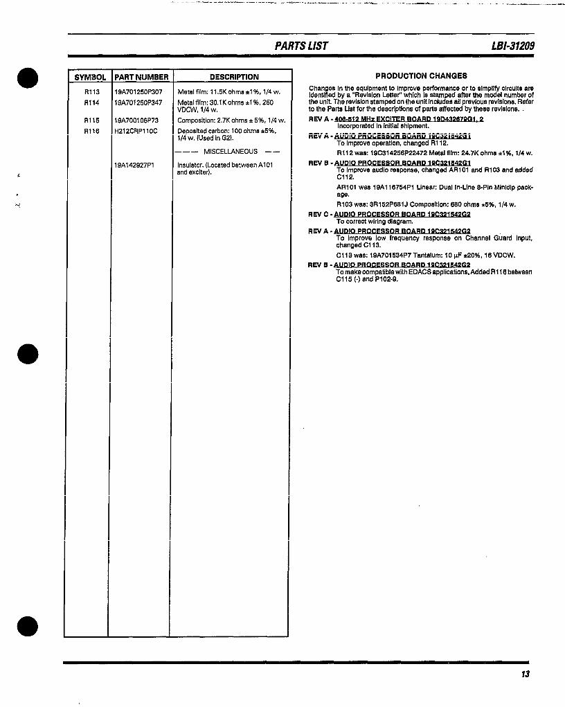
SYMBOL PART NUMBER DESCRIPTION
---- CAPACITORS ---
Cl01 19A116192P1 Ceramic: 0.01 pF t20%, 50 VDCW; sim to Erie 8121 Special.
Cl02 lOAl34202F6 Tantalum: 22 pF +20%. 15 VDCW.
Cl03 19A116192P1 Ceramic: 0.01 pF ~20%. 50 VDCW; sim to Erie 8121 Special.
Cl04 19A116192P2 Ceramic: 470 pF t20%, 50 VDCW: thru sim to Erie El?-A050-W5R-471 M. Cl12
Cl14 1 DA701 534P7 Tantalum: IO FF +20%, 16 VDCW.
Cl15 l9Al16192Pl Ceramic: 0.01 pF t20%. 50 VDCW; sim to Erie 8121 Special.
Cl16 1QAll6l92Pl3 Ceramic: 1000 pF *IO%. 50 VDCW; sim to Erie8121-A050-W5R-?02K.
Cl17 1 9A134202P6 Tantalum: 22 pF ~20%. 15 VDCW.
CIIQL 19A116856P30J8 Ceramic disc: 30 pF ~5%. 500 VDCU tamp. coef -80 PPM. (Used in Gl).
CllQH 19A116656P27J6 Ceramic disc: 27 pF t5%, 500 VDCV\I temp. coef -80 PPM. (Used in G2).
Cl19 19A700013P15 Phenoiic: 1.50 pF t 5%. 500 VDCW.
Cl20 19A116192P1 Ceramic: 0.01 pF ~20%. 50 VDCW; sim to Erie 8121 Special.
Cl2lL 19Al16656P30JQ Ceramic disc: 30 pF +5%, 500 VDCW temp. coef -80 PPM. (Used in Gl).
Cl21H 19A116656P27J8 Ceramic disc: 27 pF ~5%. 500 VDCW temp. coef -80 PPM. (Used in G2).
C122L 19A116656F’24J6 Ceramic disc: 24 pF +5%, 500 VDCW temp. coef -80 PPM (Used In Gl).
Cl 22H 1 9Al16656P2OJQ Ceramic disc: 20 pF +5%, 500 VDCW temp. coef -80 PPM (Used in G2).
Cl24 19A700105P34 Mica: 100 pF ~5%. 500 VDCW.
Cl25 19All6192P4 Ceramic: 2700 pF +20%, 50 VDCW; sim to Erie 8121-M050-W5R-272K,
Cl26 19A116192P2 Ceramic: 470 pF 220%. 50 VDCW; sim to Erie 81 l-A050-W5R-471 M.
Cl27 lQA116192P4 Ceramic: 2700 pF t20%, 50 VDCW; sim to Erie 812l-M05O-W5R-272K.
Cl28 19A116192P1 and
Ceramic: 0.01 pF t20.%, 50 VDCW;
Cl29 sim to Erie 6121 Special.
Cl30 1 QA701534P4 Tantalum: 1 pF t 20%. 35 VDCW.
Cl31 5491601P116 Phenolic: 0.75 pF * 5%. 500 VDCW.
Cl32 19A116192P13 Ceramic: 1000 pF tl O%, 50 VDCW; sim to Erie 6121-A050-W5R-102K.
Cl33 lSAlI6655P7 Ceramic disc: 150 pF i 20%, 1000 VDCW: sim to RMC Type JF Discap.
Cl34 19A116655P19 Ceramic disc: 1000 pF * 20%. 1000 VDCW; sim to RMC Type JF Discsp.
Cl35 19A116192P13 Ceramic: 1000 pF *IO%, 50 VDCW; sim to Erie 8121-A050-W5R-102K.
Cl36 19All6655P19 Ceramic disc: 1000 pF + 20%, 1000 VDCW: sim to RMC Type JF Discap.
Cl37 19A700013P11 Phenolic: 0.66 pF t 5%. 500 VDCW.
Cl38L lQAll6656P56.J8 Ceramic disc: 56 pF t5%, 500 VDCW, temp. coef -80 PPM. (Used in GI).
* COMPONENTS, ADDED, DELETED OR CHANGED BY PRODUCTION CHANQES
SYMBOL PART NUMBER DESCRIPTION
Cl38H 19A116656P39J8 Ceramic disc: 39 pF r5%. 500 VDCW. temp. coef -80 PPM (Used in G2).
Cl39 19A116192P2 Ceramic: 470 pF t20%, 50 VDCW; sim to Erie 811A050-W5R-471 M.
Cl41 lOA116655P7 Ceramic disc: 150 pF * 20%. 1000 VDCW; sim to RMC TYpe JF Discap.
Cl43L 19A700105P26 Mica: 47 pF +5%, 500 VDCW. (Used in Gl).
Cl43H 19A700105P23 Mica: 39 pF +5%, 500 VDCW. (Used in G2).
Cl44 19All6192Pl7 Ceramic: 0.047 FF tlO%, 50 VDCW, sim to Erie 8101 -A056X5R331 K.
Cl45L lQAl16656P22J8 Ceramic disc: 22 pF rS%, 500 VDCW, temp. coef -80 PPM. (Used in Gl).
Cl45H 19A116656Pl5J6 Ceramic disc: 15 pF t5%, 500 VDCW, temp. coef -80 PPM. (Used in G2).
Cl46 19A700013P10 Phenolic: 0.56 pF t 5%, 500 VDCW.
C147L 1QAll6656P3OJ6 Ceramic disc: 30 pF ~5%. 500 VDCW, temp. coef -80 PPM. (Used in Gl).
Cl47H lQAll6656P15J8 Ceramic disc: 15 pF +5%, 500 VDCW, temp. coef -80 PPM. (Used in G2).
Cl48 1 SAI 16656P3OJQ Ceramic disc: 30 pF t5%, 500 VDCW, temp. coef -80 PPM.
Cl49 lQA116655P7 Ceramic disc: 150 pF * 20%. 1000 VDCW; sim to RMC Type JF Discap.
Cl51 19A116192P7 Ceramic: 330 pF +lO%, 50 VDCW; sim to Erie QIOI-A050-W5R-331 K.
Cl52L 19All6656P4JO Ceramic disc: 4 pF ~0.5 pF, 500 VDCVl temp. coef 0 PPM. (Used in Gl).
C152H l9All6656P3.iO Ceramic disc: 3 pF +0.5 pF, 500 VDCVI temp. coef 0 PPM. (Used in G2).
Cl54 19A116655P19 Ceramic disc: 1000 pF L 20%. 1000 VDCW; sim to RMC Type JF Discap.
Cl 55 1 SA7OOOO8Pl Variable: 2.04 to 9.9 pF, 250V peak.
Cl56 19A700013P14 Phenolic: 1.20 pF * 5%. 500 VDCW.
Cl57 19A700008P1 Veriable: 2.04 to 9.9 pF, 26OV peak.
C156L lSA700233PS Ceramic:470 pF f 20%. 60 VDCW. (Used in GIL
Cl 58H 1 SA700233P4 Ceramic: 330 pF i20%, 50 VDCW. (Used in G2).
Cl6lL 19A116656P6J8 Ceramic disc: 6 pF i 5%. 500 VDCW; temp. coef -80 PPM. (Used in Gl).
Cl6lH 19A116656P5J8 Ceramic disc: 5 pF * 5%. 500 VDCW; temp. coef -80 PPM. (Used in G2).
Cl62 IQAI 16656P47JI Ceramic disc: 47 pF + 5%, 500 VDCW; temp. coef -1 SO PPM.
Cl63 1 SAI 16656P3OJQ Ceremic disc: 30 pF l 5%, 500 VDCW, temp. coef -80 PPM.
Cl54 lSAll6655F’7 Ceramic disc: 150 pF t 20%, 1000 VDCW; sim to RMC Type JF Discap.
Cl65 19A700105P14 Mica: 18 pF *5%, 500 VDCW.
Cl66L lSAll6656P4JO Ceramic disc: 4 pF +0.5 pF. 500 VDCW, temp. coef 0 PPM. (Used in Gl).
Cl66H lSA116656P3JO Ceramic disc: 3 pF +0.6 pF, 600 VDClA temp. coef 0 PPM. (Used in G2).
Cl67 19A700008P1 Variable: 2.04 to 9.9 pF, 26OV peak.
Cl68 19All6656P47Jl Ceramic disc: 47 pF * 5%. 500 VDCW;. temp. coef -150 PPM.
0
10
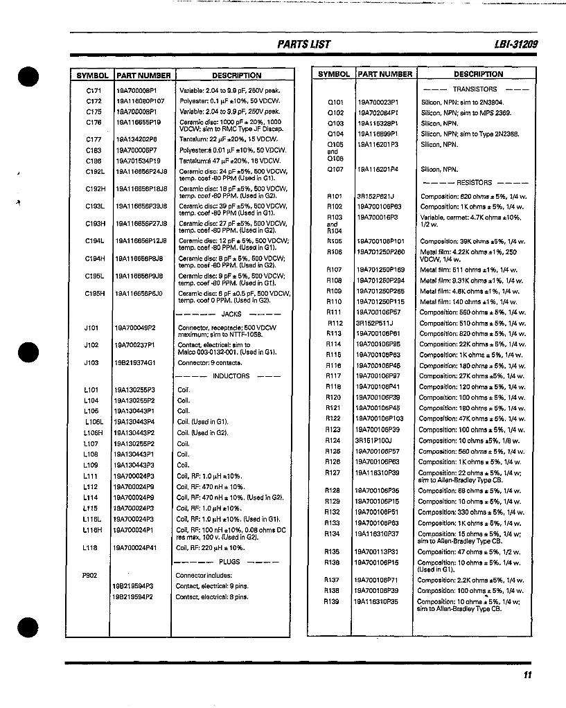
PARTS LIST LB/-31209
SYMBOL PART NUMBER DESCRIPTION
Cl71 19A700008Pl Variable: 2.04 to 9.9 pF, 250V peak.
Cl72 19A11608OP107 Polyester: 0.1 pF +lO%, 50 VDCW.
Cl75 19A700008Pl Variable: 2.04 to 9.9 pF, 250V peak.
Cl76 19A116655P19 Ceramic disc: 1000 pF I 20%, 1000 VDCW: sim to RMC Type JF Discap.
Cl77 19A134202P6 Tantalum: 22 pF *20%, 15 VDCW.
Cl83 lSA700005P7 Polyester:& 0.01 pF +lO%, 50 VDCW.
Cl86 19A701534PlS Tantalum:& 47 pF *20%, 16 VDCW.
C192L 18A116666P24JE Ceramic disc: 24 pF t5%, 500 VDCW, temp. coef -60 PPM (Used in Gl).
C192H lSA116656P18JE Ceramic disc: 18 pF *5%, 500 VDCW, temp. coef -60 PPM. (Used in G2).
C193L 19A116656P39JE Ceramic disc: 39 pF *5%, 500 VDCW, temp. coef -60 PPM (Used in Gl).
Cl 93H 1 QA116656P27JE Ceramic disc: 27 pF t5%, 500 VDCW, temp. coef -80 PPM. (Used in G2).
C194L 1 QA116656Pl2JE Ceramic disc: 12 pF t 5%, 500 VDCW temp. coef -80 PPM. (Used in Gl).
C194H lSA116656P8JE Ceramic disc: 8 pF * 5%. 500 VDCW; temp. coef -80 PPM. (Used in G2).
C195L lQA116656PQJ8 Ceramic disc: 9 pF * 5%, 500 VDCW; temp. coef -60 PPM. (Used in Gl).
C195H lSA116656P6JO Ceramic disc: 6 pF a0.5 pF, 600 VDCr temp. coef 0 PPM. (Used In G2).
----- JACKS ----
JlOl 19A700049P2
J102 1 QA700237Pl
J103 19821937461
Connector, receptacle; 500 VDCW maximum; sim to NlTF-1058.
Contact, electrical: sim to Malco 003-0132-001. (Used in Gl).
Connector: 9 contacts.
---- INDUCTORS ---
LlOl lQA130255P3
L104 19A130255P2
L105 19A130443Pl
L105L lSA130443P4
L106H 19A130443P2
L107 1 QA130255P2
L108 lSA130443Pl
LlOQ I QA130443P3
Llll 1 QA700024P3
L112 lQA700024PS
L114 lQA700024PQ
L115 1 SA700024P3
L116L 1 SA700024P3
L116H 1 QA700024Pl
L116 19A700024P41
Coil.
Coil.
Coil.
Coil. (Used in Gl).
Coil. (Used in G2).
Coil.
Coil.
Coil.
Coil, RF: 1 .O FH alO%.
Coil, RF: 470 nH * 10%.
Coil, RF: 470 nH t 10%. (Used in G2).
Coil, RF: l.OpH tlO%.
Coil, RF: 1.0 pH alO%. (Used in Gl).
Coil, RF: 100 nH tlO%, 0.08 ohms DC res max. 100 v. (Used in G2).
Coil, RF: 220 pH * 10%.
----- PLUGS ----
P902
198219594P3
19B219594P2
Connector includes:
Contact, electrical: 9 pins.
Contact, electrical: 6 pins.
SYMBOL PART NUMBER DESCRIPTION
--- TRANSISTORS ---
0101
0102
0103
Q104
Q105 and 0106
Q107
19A700023Pl
lSA702084P1
19A116326Pl
19A116899Pl
lSA1162OlP3
lQA116201P4
Silicon, NPN: sim to 2N3804.
Silicon, NPN: sim to MPS 2369.
Silicon, NPN.
Silicon, NPN; sim to Type 2N2368.
Silicon, NPN.
Silicon, NPN.
----RESISTORS ----
RlOl 3R152P621J Composition: 620 ohms t 5%. l/4 w.
R102 19A700106P63 Composition: 1 K ohms * 5%, l/4 w.
R103 lSA700016P3 Variable, cermet: 4.7K ohms tlO%, and l/2 w. R104
R105 19A700106P101 Composition: 39K ohms ~5%. l/4 w.
R106 lQA70125OP260 Metal film: 4.22K ohms tl %, 250 VDCW, l/4 w.
R107 lQA70125OP169 Metal film: 511 ohms ~1%. l/4 w.
R108 19A70125OP294 Metal film: 9.31 K ohms tl %, l/4 w.
R109 19A70125OP265 Metal film: 4.6K ohms tl %, l/4 w.
RllO lQA70125OP115 Metal film: 140 ohms tl%, l/4 w.
Rlll lSA700106P57 Composition: 560 ohms t 5%. l/4 w.
R112 3R152P611J Composition: 510 ohms t 5%. l/4 w.
R113 lSA700106P61 Composition: 820 ohms f 5%, l/4 w.
R114 lQA700106P95 Composition: 22K ohms t 5%. l/4 w.
R115 lSA700106P63 Composition: 1 K ohms t 5%, l/4 w.
R116 lSA700106P45 Composition: 180 ohms t 5%, l/4 w.
R117 lQA700106P97 Composition: 27Kohms t5%. l/4 w.
R118 19A700106P41 Composition: 120 ohms t 5%, l/4 w.
R120 lQA700106P39 Composition: 100 ohms t 5%. l/4 w.
R121 lQA700106P46 Composition: 180 ohms * 5%. l/4 w.
R122 19A700106P103 Composition: 47K ohms t 5%, l/4 w.
R123 lSA700106P39 Composition: 100 ohms t 5%, l/4 w.
R124 3R151PlOOJ Composition: 10 ohms ~5%. l/8 w.
R125 1 SA700106P57 Composition: 560 ohms t 6%. 114 w.
R126 lSA700106P63 Composition: 1 K ohms t 5%. 114 w.
RI27 lQA11631OP39 Composition: 22 ohms t 5%, l/4 w; sim to Allen-Bradley Type CB.
R128 1 QA700106P35 Composition: 68 ohms t 5%. l/4 w.
R129 lQA700106P15 Composition: 10 ohms t 5%. l/4 w.
R132 lQA700106P51 Composition: 330 ohms f 5%, l/4 w.
R133 1 QA700106P63 Composition: 1 K ohms t 5%. l/4 w.
R134 lQA11631OP37 Composition: 15 ohms t 5%, l/4 w; sim to Allen-Bradley Type CB.
R135 1 QA700113P31 Composition: 47 ohms t 5%, l/2 w.
R136 lQA700106P15 Composition: 10 ohms t 5%, l/4 w. (Used in Gl).
R137 lQA700106P71 Composition: 2.2K ohms 25%. l/4 w.
R138 lSA700106P39 Composition: 100 ohms2 5%, l/4 w.
R139 19A116310P35 Composition: 10 ohms * 5%. l/4 w; sim to Allen-Bradley Type CB.
11

LB/-31209 PARTS LIST
SYMBOL PART NUMBER DESCRIPTION
R141 lQA700113P31 Composition: 470hms * 5%, l/2 w.
R142 lSA700106P63 Composition: 1 Kohms t 5%. l/4 w.
R143 19A700113P49 Composition: 270 ohms t 5%. l/2 w.
---- THERMISTOR ---
RTlOl 6490828P54 Thermistor: 50 ohms t 10%. color code blue; sim to Carborundum Type BO807J-16.
--- TRANSFORMERS --
TlOl
T102
T103
T104
T105
T106 and T107
1 SC3071 7OP305 Coil, RF: variable, wire size No. 20 AWG; sim to Paul Smith Co. Sample No. 082574DS-2.
1 SC3071 7OP306 Coil, RF: variable, wire size No. 20 AWG; sim to Paul Smith Co. Sample No. 092574-DS-3.
1 SC3071 7OP307 Coil, RF: variable, wire size No. 20 AWG; sim to Paul Smith Co. Sample No. 092574DS-4.
1 QC307169P202 Coil, RF: variable, wire size No. 20 AWG; sim to Paul Smith Co. Sample No. 092574DS-5.
19C307169P203 Coil, RF: variable, wire size No. 20 AWG; sim to Paul Smith Co. Sample No. 092574DS-6.
lQC307169P204 Coil, RF: variable, wire size No. 20 AWG; sim to Paul Smith Co. Sample No. 100374DS-8.
------SOCKETS ----
x(101 thru x/108
Part of mechanical construction.
---- CRYSTALS ----
YlOl thru Y108
19A13060663
1 SA130605G4
ISA1 30605G5
1 QAI 30605G6
FM ICOM, Internaliy compensated, * 2 PPM, 406450 MHz.
FM ICOM, Internally compensated, t 2 PPM, 460.470 MHz.
FM ICOM, Internally compensated, t 2 PPM, 470-4494 MHz.
FM ICOM, Internally compensated, * 2 PPM, 494-512 MHz.
----- FILTER ----
ZlOl lQA134666P2 Frequency network: selective, 460600 MHz resonant freq, 500 VDCW; sim to DilectronTCBOl:NPO:270J:SLAC.
--- MISCELLANEOUS --
19C331133Gl
lSA701544P7
lQA701332Pl
18A701785Pl
lEC331287Gl
lQA121175P24
Shield.
Can, drawn aluminum.
Insulator disk.
Contact, electrical; sim to MolexOB506404.
Assembly shield.
Insulator plate.
SYMBOL PART NUMBER DESCRIPTION
AUDIO PROCESSOR lSC221642Gl,G2
--lNTEGRATEDClRCUlTS --
AR101 19A116754P2 Linear, Dual 741C OP AMP; sim to MC1458SPl High Slew Rate OP AMF
--- CAPACITORS ----
Cl01 Tt344ACP333J Polyester: .033 uF *5%, 50 VDCW.
Cl02 5491674P36 Tantalum: 3.3 FF t 20%, 10 VDCW; and Cl03
sim to Sprague Type 162D.
Cl04 T644ACP347J Polyester: .047 pF t5%, 50 VDCW.
Cl05 T644ACP333J Polyester: .033 FF r5%, 50 VDCW. (Used in Gl 1.
Cl06 5491674P28 Tantalum: 1 pF +20%, 25 VDCW: sim to Sprague Type 162D. (Used in Gl).
Cl07 5496267P9 Tantalum: 3.3 pF * 20%. 15 VDCW; sim to Sprague Type 150D.
Cl08 T644ACP268-J Polyester: .0068 pF +5%. 50 VDCW.
Cl09 1 QA701602P20 Ceramic: 1000 pF ~10%. 1000VbCW.
Cl10 5491674P36 Tantalum: 3.3 pF * 20%. 10 VDCW; sim to Sprague Type 162D. (Used in Gl).
Cl11 T644ACP368J Polyester: .068 FF +5%, 50 VDCW.
Cl12 lSA143491 P6JO Ceramic: 6 pF ~5%. temp. coef 0 PPM
Cl13 lSA701534PQ Tantalum: 47 FF t20%, 6.3 VDCW. (Used in 02).
Cl14 5491674P36 Tantalum: 3.3 FF t 20%. 10 VDCW; sim to Sprague Type 162D. (Used in G2).
Cl15 1 QA701534P8 Tantalum: 22 FF +20%, 16 VDCW. (Used in 02).
w--w DIODES -----
CR101 lQA11525OPl Silicon, fast recovery 225 mA, 50 PIV. and CR102
-----PLUGS -----
P102 lSA116859P76 Connector, printed wiring: 9 contacts rated at 5 amps; sim to MolexOQ-52-3091.
----RESISTORS ----
RlOl 19A134231 P223J Deposited carbon: 22K ohms t5%, l/8 w.
R102 19A700106P95 Composition: 22K ohms + 5%. l/4 w.
R103 lQA700108P55 Composition: 470 ohms t 5%. l/4 w.
RIO4 lQA70125OP369 Metal film: 51 .l K ohms +l %, II4 w.
R105 1 QA70126OF303 Metal film: 10.5K ohms tl%, l/4 w.
RI06 lSA70125OP311 Metal film: 12.7K ohms tl %, l/4 w.
R107 1 QA70125OP303 Mete1 film: 10.5K ohms tl%, l/4 w.
R108 19A7012508269 Metal film: 5.11 K ohms tl%, l/4 w.
RI09 3R152P132J Composition: 1.3K ohms ~5%. l/4 w.
RllO 19A70125OP269 Metal film: 5.11 K ohms ~1%. l/4 w.
Rlll 19A700106P91 Composition: 15K ohms t 5%. l/4 w.
R112 lQA70125OP339 Mets1 film: 24.9K ohms ~1%. l/4 w.
12
c
PARTS LIST LB/-31209
SYMSOI SYMBOL 1 PART NUMBER 1 DESCRIPTION DESCRIPTION I I PART NUMBE
19A70125OP307
19A70125OP347
R113 R113
R114 R114
19A70125OP307 Metal film: 11.5K ohms +l %, l/4 w. Metal film: 11.5K ohms +l %, l/4 w.
19A70125OP347 Metal film: 30.lK ohms tl%, 250 Metal film: 30.lK ohms tl%, 250 VDCW, l/4 w. VDCW, l/4 w.
19A700106P73 19A700106P73 Composition: 2.7K ohms * 5%. 114 w. Composition: 2.7K ohms * 5%. l/4 w.
H21 PCRPl 1 OC H21 PCRPl 1 OC Deposited carbon: 100 ohms ~5%. Deposited carbon: 100 ohms l 5%, 114 w. (Used in G2). l/4 w. (Used in G2).
I --- MISCELLANEOUS -- --- MISCELLANEOUS --
19A142927Pl Insulator. (Located between Al 01 Insulator. (Located between Al 01 and exciter). and exciter).
R115 R115
R116 R116
PRODUCTION CHANGES
Changes In the equipment to Improve performance or to slmpllfy &cults are ldentlfled by a “Revision Letter” which Is stam d after the model number of the unlt. The revision stamped on the unit lnclu 8” es all prevlous revlslons. Refer to the Parts Llst for the descrlptlons of parts affected by these revlslone. -
EVA-~ Incorporated In lnltlal shipment.
REVA.AUDIO To Improve operation, changed R112.
RI 12 was: lQC314256P22472 Metal film: 24.7K ohms +l%, l/4 w.
RBVB-wPRQCESSOR.BOARD To improve audio response, changed AR101 and RIO3 and added c112.
AR1 01 was lQAl16754Pl Linear: Dual In-Line 8-Pin Minidip pack- age.
R103 was: 3R152P88lJ Composition: 680 ohms t5%, l/4 w.
REVC-AUDIO To correct wiring diagram.
RBVA-AUDIO To improve low frequency response on Channel Guard Input, changed Cl 13.
Cl13 was: lQA701534P7 Tantalum: 10 PF +20%, 16 VDCW.
RBVB-AUDIOPRDCESSOR To make compatible with EDACS applications,Added Rll6 between Cl15 (-) and P102-9.
Related Documents