UNIVERSIDAD AUTONÓMA DE MADRID FACULTAD DE CIENCIAS Departamento de Física de la Matería Condensada Magnetic Force Microscopy study of layered superconductors in vectorial magnetic fields Memoria presentada por Alexandre Correa Orellana para obtener el título de Doctor en Física Directores: Dr. Hermann Jesús Suderow Dr. Carmen Munuera López Madrid, 2017

Welcome message from author
This document is posted to help you gain knowledge. Please leave a comment to let me know what you think about it! Share it to your friends and learn new things together.
Transcript
UNIVERSIDAD AUTONÓMA DE MADRID
FACULTAD DE CIENCIAS
Departamento de Física de la Matería Condensada
Magnetic Force Microscopy study of layered
superconductors in vectorial magnetic fields
Memoria presentada por
Alexandre Correa Orellanapara obtener el título de Doctor en Física
Directores:
Dr. Hermann Jesús Suderow
Dr. Carmen Munuera López
Madrid, 2017

Acknowledgements
En primer lugar me gustaría dar las gracias a mis directores de tesis, la Dra. Car-
men Munuera y el Dr. Hermann Suderow por depositar en mí la confianza para
realizar este trabajo de investigación. Vuestra dedicación, profesionalidad y amplios
conocimientos han sido fundamentales para el desarrollo de esta tesis y todo un ejem-
plo para mí.
Doy las gracias también a la Dra. Isabel Guillamón por todo el tiempo empleado
en mi tesis y por su dedicación y paciencia. También me gustaría agradecer las
enseñanzas y el apoyo continuado de los Dres. Federico Mompeán, Norbert Nemes y
Mar García Hernández.
Doy las gracias al personal del Instituto de Ciencia de Materiales de Madrid
(ICMM) y de la Universidad Autónoma de Madrid (UAM). Doy gracias a todos los
compañeros con los que he coincidido en el laboratorio, Rafa, Chema, Pepe, Edwin,
Víctor, Jon, Antón, Félix, Jesús, Elena, Federico y Roberto.
I would like to thank the Weizmann Institute Collaborators, Dr. Eli Zeldov, Dr.
Jonathan Anahory and Dr Lior Embon for their collaboration. I would also like to
thank Dr. Kadowaki for providing us with the nice Bi-2212 single crystal measured
during the thesis. I would like to thank Dr. Paul Canfield for suggesting us to measure
Co doped CaFe2As2 and helping us to understand what was going on.
Me gustaría agradecer especialmente al Dr. Sebastián Vieira por darme la opor-
tunidad de empezar mi carrera en el mundo científico hace 5 años.
Por último, me gustaría agradecer a los proyectos de investigación Anisometric
iii

CHAPTER 0. Acknowledgements iv
permanent hybrid magnets based on inexpensive and non-critical materials (AM-
PHIBIAN) (Ref. NMBP-03-2016) y Graphene Flagship (Grant No. 604391) finan-
ciados por la Unión Europea, gracias a los cuales he podido realizar mi tesis doctoral.
Abstract
This thesis is focused on the set-up and use of a cryogenic magnetic force microscope
(MFM) in a three axis vector magnet. We have studied superconducting layered and
quasi-two dimensional compounds. In particular, we address the superconducting
properties of graphene deposited on an isotropic s-wave superconductor β−Bi2Pd, of
a layered cuprate superconductor (BiSr2CaCu2O8), of a layered iron based material
(Ca(Fe0.965Co0.035)2As2) and of the s-wave superconductor β−Bi2Pd.
MFM measures the magnetic properties of a surface by tracing the force when a
magnetic tip is scanned over a magnetic sample. The interaction is mutual, the tip
feels the magnetic properties of the sample and viceversa. By adjusting the scanning
height, we can go from a non-invasive situation to manipulation, very much the same
as in atomic manipulation using a STM. Here, in a MFM, the objects that are usually
studied are much larger than atoms. Magnetic interactions usually extend over larger
distances and therefore often the spatial resolution is of the order of the nm or above.
This tool is ideal to study the magnetic profile generated by superconductors in the
mixed state. Abrikosov vortices have a magnetic shape that is determined by the
penetration depth, which is most often well above the nm range.
Here we are interested in the properties specific to two-dimensional and quasi two-
dimensional superconducting systems. The associated confinement of superconduc-
tivity brings about new aspects. An important one is that, in the limit of extremely
thin samples, the penetration depth often diverges. This makes the MFM useless to
identify vortices or study magnetic textures, because the magnetic contrast decreases
accordingly. Thus, instead of using single layers, we have focused on layered super-
conductors and hybrid structures combining a bulk superconductor with a 2D system
v

CHAPTER 0. Abstract vi
as graphene. Another important aspect is that vortices are no longer lines of magnetic
flux but disks. This implies that their mobility and pinning properties change consid-
erably. Also, highly anisotropic properties can produce structural transitions, which
are often of first order and can lead to coexistence of superconducting and normal do-
mains. The MFM is there an ideal tool, with which we can make combined magnetic
and structural studies, the latter by measuring the non-magnetic interaction between
tip and sample, and making Atomic Force Microscopy (AFM). Finally, interactions
might induce novel p-wave or unconventional superconducting states. This has been
a recent focus, with the discovery of Majorana end states in proximity induced small
superconducting structures. The spectroscopic features of such structures are well
addressed in literature and it is generally acknowledged that studying the magnetic
textures is the next important step. By inducing superconductivity in graphene, we
have searched for unconventional behavior.
In the third chapter of the thesis, we have focused on the exfoliation and deposition
of layered superconductors and on the study of graphene/superconductor interfaces.
2D superconductivity in thin films and crystal flakes has attracted the attention of
many researchers in the last decade [1–9]. For example, superconducting crystals like
BSCCO or TaS2 have been successfully exfoliated down to a single layer and deposited
in a substrate in the past [10–12]. In addition, a lot of work has been done trying
to induce superconductivity in graphene in contact with a superconductor due to the
proximity effect [1, 2, 13–17]. In this thesis, we have measured the magnetic profile
of a Bi-2212 flake below the superconducting transition, developed an experimental
procedure to localize graphene flakes deposited on top of a β-Bi2Pd single crystal and
demonstrated the possibility to depositing thin flakes of the β-Bi2Pd superconductor
on a substrate.
The vortex distribution in a superconductor at very low fields is still an open
debate in the scientific community. For example, bitter decoration experiments per-
formed in the single gap, low-κ superconductor, Nb, shows areas where flux expulsion
coexists with regions showing a vortex lattice. Moreover, Scanning Hall Microscopy
experiments have shown vortex chains and clusters in ZrB12 (0.8<κ<1.12) at very
low fields [18]. Both experiments were explained with the existence of an attractive

CHAPTER 0. Abstract vii
term in the vortex-vortex interaction in superconductors with κ < 1.5 . This regime
is known as the Intermediate Mixed State. On the other hand, the existence of vortex
free areas between cluster and stripes of vortices at very low fields was also reported
in the multigap superconductor MgB2 [19–21]. In this case, the authors propose that
this behavior corresponds to a new state that they called type 1.5 superconductivity,
due to the existence of two different values of the Ginzburg-Landau parameter, κ,
for the two gaps of the compound. In addition, a recent theoretical work has also
proposed that pinning may have an important role in the formation of the vortex
patterns in MgB2 [22]. Comparatively, β−Bi2Pd has a small, yet sizable, value of
κ≈ 6. It has very weak pinning and is a single gap isotropic superconductor [23–25].
This allows us to characterize the vortex distribution at very low fields in a material
with only one gap and a moderate value of κ for the first time. We have found vortex
clusters and stripes as in the case of low-κ or multigap superconductors. But, in this
case, they are associated with local changes in the value of the penetration depth of
the superconductor. We have also measured the vortex lattice at low temperatures
of a β-Bi2Pd single crystal with a graphene sheet deposited on top and found that
the penetration depth increases, particularly at steps and wrinkles of the graphene
surface. These results are presented in chapter 4.
Ca(Fe0.965Co0.035)2As2 is an iron based compound with extremely high sensitiv-
ity to pressure and strain. Due to the presence of Ca ions, small pressures result
in dramatic changes in the ground state of the system. We have characterized the
formation of alternating superconducting antiferromagnetic domains at low temper-
atures and related them with the separation of the material in two structural phases.
The results are collected in chapter 5.
In the last chapter of the thesis, we focus on the local manipulation of supercon-
ducting vortices in the high-temperature cuprate superconductor BiSr2CaCu2O8. It
has a two-dimensional layered structure, with superconductivity taking place in the
copper oxide planes. When a magnetic field is applied tilted with respect to the c
crystallographic axis, the vortex lattice decomposes into two systems of vortices, per-
pendicular to each other. There are Josephson, coreless vortices parallel to the layers
and Abrikosov vortices located in the copper oxide planes, called pancake vortices. In

CHAPTER 0. Abstract viii
our work, we use the MFM tip to manipulate pancake vortices at low temperatures
and have determined the force needed to move combined pancake and Josephson
vortex lattices.

Contents
Acknowledgements iii
Abstract v
1 Introduction 1
1.1 Historical remarks . . . . . . . . . . . . . . . . . . . . . . . . . . . . . 1
1.2 Superconducting theories . . . . . . . . . . . . . . . . . . . . . . . . . 2
1.2.1 Ginzburg-Landau Theory . . . . . . . . . . . . . . . . . . . . . 2
1.2.1.1 Coherence length . . . . . . . . . . . . . . . . . . . . . 3
1.2.1.2 Penetration depth . . . . . . . . . . . . . . . . . . . . 4
1.2.1.3 Type I and type II superconductors . . . . . . . . . . 5
1.2.1.4 Vortex lattice . . . . . . . . . . . . . . . . . . . . . . . 6
1.2.2 BCS theory . . . . . . . . . . . . . . . . . . . . . . . . . . . . . 7
1.2.2.1 Superconducting gap . . . . . . . . . . . . . . . . . . 8
1.3 Intermediate and Intermediate Mixed States . . . . . . . . . . . . . . . 9
1.3.1 Intermediate State . . . . . . . . . . . . . . . . . . . . . . . . . 9
1.3.2 Intermediate Mixed State . . . . . . . . . . . . . . . . . . . . . 11
1.4 Anisotropic Superconductors . . . . . . . . . . . . . . . . . . . . . . . 12
1.4.1 Pancake vortices . . . . . . . . . . . . . . . . . . . . . . . . . . 13
1.4.2 Josephson vortices . . . . . . . . . . . . . . . . . . . . . . . . . 13
1.4.3 Crossing lattice . . . . . . . . . . . . . . . . . . . . . . . . . . . 14
1.5 Iron Based Superconductors . . . . . . . . . . . . . . . . . . . . . . . . 16
1.5.1 Phase diagram . . . . . . . . . . . . . . . . . . . . . . . . . . . 18
1.5.1.1 Electronic structure . . . . . . . . . . . . . . . . . . . 19
1.5.1.2 Magnetism . . . . . . . . . . . . . . . . . . . . . . . . 20
1.5.1.3 Superconducting gap . . . . . . . . . . . . . . . . . . 22
1.6 Induced superconductivity in 2D systems . . . . . . . . . . . . . . . . 23
ix

Contents x
1.6.1 Induced superconductivity on graphene . . . . . . . . . . . . . 23
1.7 Motivation . . . . . . . . . . . . . . . . . . . . . . . . . . . . . . . . . 26
2 Experimental methods 29
2.1 Set-up . . . . . . . . . . . . . . . . . . . . . . . . . . . . . . . . . . . . 29
2.1.1 Cryostat, VTI and vibration isolation stage . . . . . . . . . . . 30
2.1.2 Three axis superconducting vector magnet . . . . . . . . . . . . 32
2.1.3 Low Temperature Microscope . . . . . . . . . . . . . . . . . . . 33
2.1.3.1 AFM probe holder . . . . . . . . . . . . . . . . . . . . 34
2.1.3.2 Sample holder . . . . . . . . . . . . . . . . . . . . . . 36
2.1.3.3 Scanning and tip oscillation system . . . . . . . . . . 36
2.1.3.4 Approaching-retracting mechanism . . . . . . . . . . . 36
2.1.3.5 Optical laser interferometer method . . . . . . . . . . 38
2.1.3.6 LT-AFM controller . . . . . . . . . . . . . . . . . . . 40
2.1.3.7 Operational modes . . . . . . . . . . . . . . . . . . . . 41
2.1.3.7.1 Dynamic mode . . . . . . . . . . . . . . . . . 41
2.1.3.7.2 MFM mode . . . . . . . . . . . . . . . . . . . 44
2.2 Characterization of MFM probes for low temperature experiments . . 46
2.2.0.1 MFM features . . . . . . . . . . . . . . . . . . . . . . 48
2.3 Crystal growth . . . . . . . . . . . . . . . . . . . . . . . . . . . . . . . 50
2.3.1 β−Bi2Pd single crystals growth . . . . . . . . . . . . . . . . . 53
2.4 Summary and conclusions . . . . . . . . . . . . . . . . . . . . . . . . . 55
3 Exfoliation and characterization of layered superconductors and
graphene/superconductor heterostructures 57
3.1 Introduction . . . . . . . . . . . . . . . . . . . . . . . . . . . . . . . . . 57
3.2 Micromechanical exfoliation . . . . . . . . . . . . . . . . . . . . . . . . 58
3.2.1 BSCCO on SiO2 . . . . . . . . . . . . . . . . . . . . . . . . . . 60
3.2.1.1 Moderate magnetic fields . . . . . . . . . . . . . . . . 60
3.2.1.2 Very low magnetic fields . . . . . . . . . . . . . . . . . 62
3.2.2 β-Bi2Pd on SiO2 . . . . . . . . . . . . . . . . . . . . . . . . . . 64
3.2.2.1 Exfoliation down to few tens of nanometers . . . . . . 64
3.2.3 Graphene on β-Bi2Pd . . . . . . . . . . . . . . . . . . . . . . . 65
3.2.3.1 Friction measurements . . . . . . . . . . . . . . . . . . 66
Contents xi
3.2.3.2 Kelvin Probe Microscopy (KPM) measurements . . . 67
3.3 Conclusions . . . . . . . . . . . . . . . . . . . . . . . . . . . . . . . . . 70
4 Vortex lattice at very low fields in the low κ superconductor β−
Bi2Pd and β−Bi2Pd/graphene heterostructures 71
4.1 Introduction . . . . . . . . . . . . . . . . . . . . . . . . . . . . . . . . . 71
4.1.1 Single and multi band superconductors in the IMS . . . . . . . 72
4.1.2 Previous works on β−Bi2Pd crystals . . . . . . . . . . . . . . 77
4.1.2.1 STM and specific heat measurements . . . . . . . . . 77
4.1.2.2 Fermi Surface . . . . . . . . . . . . . . . . . . . . . . 80
4.2 MFM and SOT characterization . . . . . . . . . . . . . . . . . . . . . 81
4.2.1 Topographic characterization . . . . . . . . . . . . . . . . . . . 81
4.2.2 Magnetic characterization . . . . . . . . . . . . . . . . . . . . . 82
4.2.2.1 Evolution of the vortex lattice with the applied mag-
netic field . . . . . . . . . . . . . . . . . . . . . . . . . 83
4.2.2.2 Penetration depth at defects . . . . . . . . . . . . . . 85
4.2.3 Origin of the variation in λ . . . . . . . . . . . . . . . . . . . . 87
4.2.4 Origin of the flux landscape . . . . . . . . . . . . . . . . . . . . 88
4.2.4.1 Evolution of the vortex lattice with the temperature . 90
4.2.4.2 Orientation of the vortex lattice . . . . . . . . . . . . 91
4.3 Electrochemical transfer of graphene on β-Bi2Pd . . . . . . . . . . . . 92
4.3.1 Characterization at room temperature . . . . . . . . . . . . . . 94
4.3.2 Characterization at low temperatures . . . . . . . . . . . . . . 95
4.4 Summary and conclusions . . . . . . . . . . . . . . . . . . . . . . . . . 99
5 Strain induced magneto-structural and superconducting transi-
tions in Ca(Fe0.965Co0.35)2As2 101
5.1 Previous studies in the parent compound CaFe2As2 . . . . . . . . . . . 102
5.1.1 Structural domains at low temperatures . . . . . . . . . . . . . 103
5.2 Previous studies in Ca(Fe1−xCox)2As2 . . . . . . . . . . . . . . . . . . 103
5.2.1 Effect of biaxial strain . . . . . . . . . . . . . . . . . . . . . . . 105
5.3 AFM/MFM studies in Ca(Fe0.965Co0.35)2As2 . . . . . . . . . . . . . . 107
5.3.1 Topographic characterization . . . . . . . . . . . . . . . . . . . 108
5.3.2 Tetragonal to orthorhombic structural transition . . . . . . . . 109
Contents xii
5.3.2.1 Origin of the topographic stripes . . . . . . . . . . . . 110
5.3.2.2 Evolution of the corrugation on the surface . . . . . . 114
5.3.3 Superconducting transition . . . . . . . . . . . . . . . . . . . . 115
5.3.3.1 Evolution with the Temperature . . . . . . . . . . . . 115
5.3.3.2 Evolution with the magnetic field . . . . . . . . . . . 117
5.3.4 Origin of the perpendicular domains . . . . . . . . . . . . . . . 118
5.4 Conclusions . . . . . . . . . . . . . . . . . . . . . . . . . . . . . . . . . 120
6 Manipulation of the crossing lattice in Bi2Sr2CaCu2O8 123
6.1 Introduction . . . . . . . . . . . . . . . . . . . . . . . . . . . . . . . . . 123
6.1.1 Interaction between JVs and PVs . . . . . . . . . . . . . . . . . 124
6.1.2 Manipulation of the crossing lattice in Bi-2212 . . . . . . . . . 125
6.1.3 Observation of crossing lattice with MFM and its manipulation 126
6.1.3.1 Force of a MFM tip on a vortex . . . . . . . . . . . . 126
6.1.3.2 Vortex manipulation in YBCO . . . . . . . . . . . . . 127
6.2 AFM/MFM studies . . . . . . . . . . . . . . . . . . . . . . . . . . . . 127
6.2.1 Topographic characterization . . . . . . . . . . . . . . . . . . . 129
6.2.2 Obtaining the Crossing Lattice . . . . . . . . . . . . . . . . . . 130
6.2.3 Evolution of the crossing lattice with the temperature . . . . . 131
6.2.4 Manipulation of the crossing lattice . . . . . . . . . . . . . . . 133
6.2.4.1 Manipulation of PVs . . . . . . . . . . . . . . . . . . . 133
6.2.4.2 Manipulation of PVs on top of JVs . . . . . . . . . . . 136
6.2.5 Manipulation with the aim to cross Josephson vortices . . . . . 138
6.2.6 Pinning of the crossing lattice at low temperatures . . . . . . . 139
6.2.7 Evolution of the PV lattice with the polar angle of the magnetic
field . . . . . . . . . . . . . . . . . . . . . . . . . . . . . . . . . 142
6.3 Conclusions . . . . . . . . . . . . . . . . . . . . . . . . . . . . . . . . . 143
7 General conclusions 145
8 Publications 176
CHAPTER 1
Introduction
1.1 Historical remarks
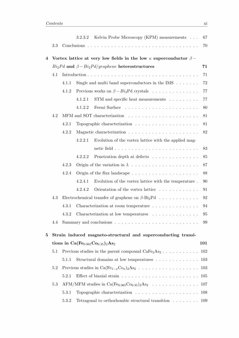
Figure 1.1: K. Onnes original
measurement of the superconducting
transition in Hg.
Superconductivity was first discovered by H. K.
Onnes in 1911 [26] after he was able to liquefy He
in his laboratory in 1908 opening a new branch
in physics, the low temperature physics. Onnes
expected a gradual approach of the resistivity to
zero with decreasing the temperature, however he
found that the resistance of Hg dropped to zero
below 4.15 K. Onnes realized that he had found a
new state of the matter characterized by zero re-
sistivity, the superconductivity. One year later he
also discovered that applying a strong magnetic
field to superconducting Hg, the normal state was
recovered. In the following years new supercon-
ducting materials were discovered: Pb, Nb etc. In 1933 Meissner and Ochsenfeld
found that if a superconductor material is cooled down below its transition temper-
ature, it expels any external magnetic field below a certain value called the critical
magnetic field, HC , [27]. This effect is called nowadays the Meissner state. Later,
superconductors where the magnetic field can penetrate the material without loosing
1
CHAPTER 1. Introduction 2
the zero resistivity were discovered and superconducting materials were split in two
categories, type I and type II superconductors.
Type I superconductors present zero resistivity and perfect diamagnetism below
TC and HC . Type II superconductors present zero resistivity below TC and the
upper magnetic critical field, HC2, but only perfect diamagnetism below the lower
magnetic critical field, HC1. Between HC1 and HC2, the magnetic field penetrates the
material in form of magnetic vortices that carry one single magnetic quantum flux,
φ0 = 2.067 · 10−15 Wb. This regime is called the mixed state. For more details see
references [28, 29].
1.2 Superconducting theories
These discoveries prompted the London brothers to propose the first phenomenolog-
ical theory in 1935 [30]. In 1950 a new superconducting theory was developed, the
Ginzburg-Landau theory [31]. It describes the superconductivity in terms of an order
parameter. Then, Bardeen Cooper and Schrieffer proposed the BCS theory, which
provides a microscopic explanation of superconductivity. [32].
1.2.1 Ginzburg-Landau Theory
Ginzburg and Landau assumed that close to the transition temperature the Gibbs
free energy density can be expanded as function of a complex parameter, ψ = |ψ|eiθ
as [31]:
GS =GN +a |ψ|2 + b
2 |ψ|4 + 1
2m∗∣∣∣(ih∇−e∗ ~A)ψ
∣∣∣ (1.1)
m∗ = 2me and e∗ = 2e are the superelectron mass and charge (me and e, are the
electron mass and charge. As we will see later, superconductivity occurs in the form of
pairs of electrons, called Cooper pairs), ~A the vector potential and a and b parameters
only dependent of the temperature with values a≈ a0[T/TC−1] and b≈ b0 near TC .
CHAPTER 1. Introduction 3
The square of the order parameter is the superconducting electron density, ns. The
order parameter ψ is zero above TC and increases as the temperature decreases below
TC . Taking the derivative of equation 1.1 with respect to the order parameter they
found what is now called the first G-L equation:
12m∗ (ih2∇2ψ−2ihe∗ ~A ·∇ψ−e∗2 ~A2ψ)−aψ− b |ψ|2ψ = 0 (1.2)
The free energy is also a minimum with respect to to the vector potential ~A.
Taking the derivative of GS with respect to ~A, we obtain the second G-L equation:
∇× (∇× ~A) + ihe∗
2m∗ (ψ∗∇ψ−ψ∇ψ∗) + e∗2
m∗~A |ψ|2 = 0 (1.3)
The G-L equations can be used to calculate the two principal length scales in a
superconductor as we will introduce in the following.
1.2.1.1 Coherence length
Let us now study the following case: a semiinfinite superconductor from x = 0 to
x =∞ and a normal metal from x = −∞ to x=0. Setting ~A = 0 in the first G-L
equation we obtain:
− h2
2m∗∇2ψ+aψ+ b |ψ|2ψ = 0 (1.4)
Since the phase, θ of the order parameter is arbitrary, we can take ψ real (θ = 0)
and therefore, ψ=ψ(x). Now, we can simplify the equation 1.4 to the one dimensional
case:
− h2
2m∗dψ2
dx2 +aψ+ b |ψ|2ψ = 0 (1.5)
which has the solution:
CHAPTER 1. Introduction 4
ψ = ψ∞tanhx√2ξ
(1.6)
where ξ is a characteristic length of ψ. ξ is called the coherence length and is one of
the two main parameters of the G-L theory. The order parameter ψ is zero inside the
normal material and increases up to ψ∞ over length scale of ξ in the superconducting
material.
1.2.1.2 Penetration depth
Now, we will consider the same semi-infinite geometry than in the previous section
but with a homogeneous magnetic field in the Z direction, which has a vector potential~A=Ay(x).
Substituting in the second G-L equation, we find:
d2Ay(x)dx2 = µ0e
∗2 |ψ|2
m∗Ay(x) (1.7)
and the solution for the vector potential inside the superconductor is:
Ay(x) =A0e(−x/λ)x (1.8)
And therefore:
Bz(x) =B0e(−x/λ) (1.9)
where A0 and B0 are constants and λ is the penetration depth, the second char-
acteristic length of the G-L theory. It represents the distance in which an external
magnetic field decreases inside the superconductor a factor e−1.
CHAPTER 1. Introduction 5
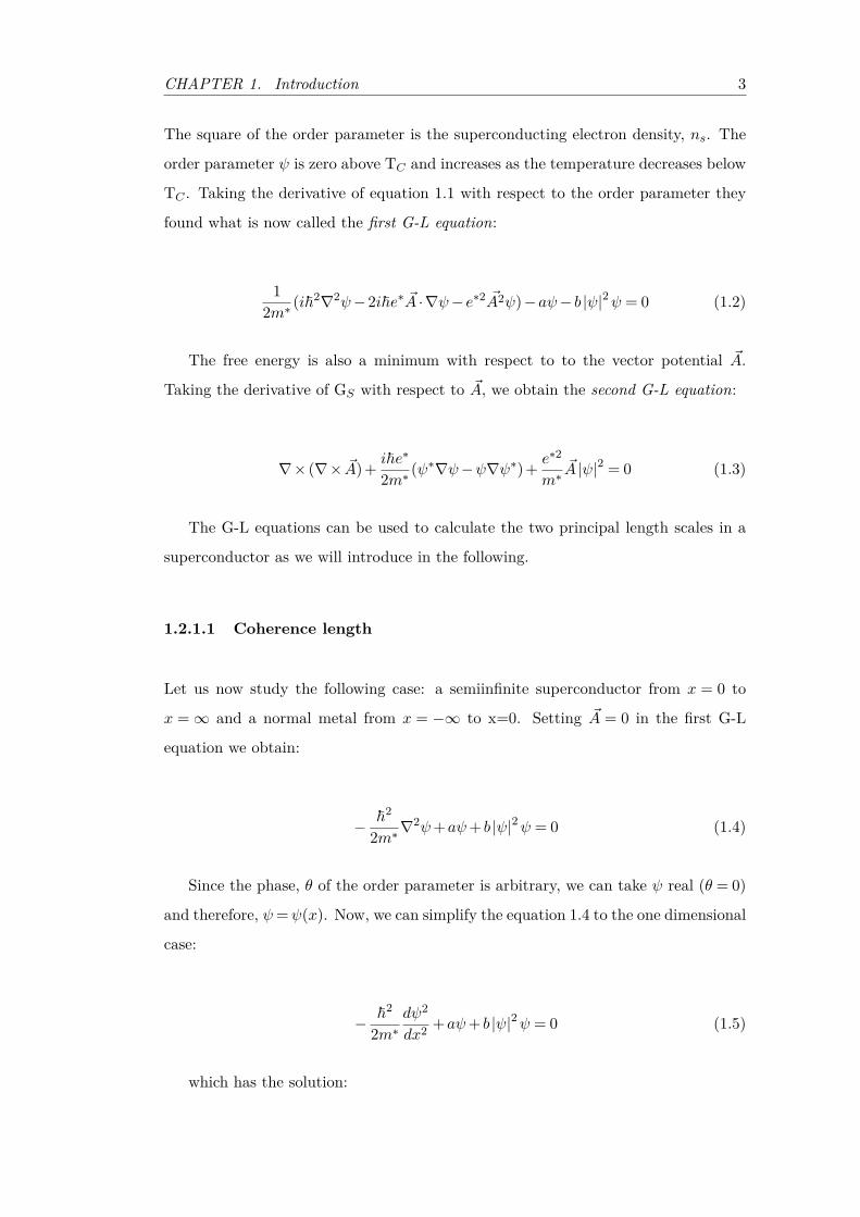
1.2.1.3 Type I and type II superconductors
Using the two characteristic lengths of the G-L theory, one can define the dimension-
less quantity:
κ= λ
ξ(1.10)
which is called the G-L parameter. Values of κ < 1/√
2 and κ > 1/√
2, separate
the G-L equations in two different branches of solutions. For κ < 1/√
2 the energy
difference between a normal and a superconducting domain is positive and for κ >
1/√
2 it is negative which means that for the superconductor becomes favorable the
formation of many small superconducting and normal domains [28].
Figure 1.2: Phase diagram for type I (left) and type II (right) superconductors.
In orange, the region presenting Meissner state. In white, the normal region. In
yellow, the mixed state region.
Solving the G-L equations for κ < 1/√
2 the B-T phase diagram for type I super-
conductors is found. In this phase diagram, there are only two regions, normal and
Meissner state, separated by the critical field, with a dependence of the temperature
following:
BC(T ) =BC(0)[1−(T
TC
)2] (1.11)
For κ> 1/√
2 a B-T phase diagram with three regions is found. The phase diagram
is separated in normal state, Meissner state and mixed state. The two first regions
CHAPTER 1. Introduction 6
are analogous to the regions in type I superconductors and the mixed state is a region
where the magnetic flux is allowed to enter into the superconductor material in form
of superconducting vortices that carry a magnetic flux φ0. Vortices are singularities
where the order parameter is suppressed and the material is in the normal state. The
three areas of the phase diagram are separated by two critical fields, with values at
zero temperature of:
BC1(0) = φ04πλ2 ln(κ) (1.12)
BC2(0) = φ02πξ2 (1.13)
Both phase diagrams are schematized in the figure 1.2.
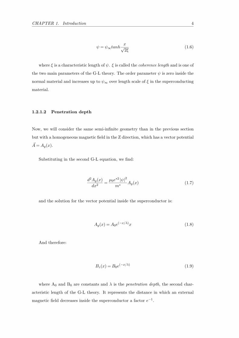
1.2.1.4 Vortex lattice
As we mention in the previous section, in type II superconductors, above a certain
value, the magnetic field is not fully expelled from the superconducting material. It
penetrates in form of magnetic vortices.
Figure 1.3: In the left panel, an scheme of the superconducting density of states
(blue) and the magnetic field (red) inside a superconducting vortex. The center of
the vortex is located at the center of coordinates in the scheme. In the right panel,
an schematic representation of the Abrikosov vortex lattice of SC vortices with a
lattice parameter a4. SC vortices are represented as yellow circles. The lattice is
schematized with dashed black lines.

CHAPTER 1. Introduction 7
Superconducting vortices are characterized by two length scales. The first one is
named ξ and provides the changes as a function of the position of the parameter ψ,
which is in turn related to the superconducting density of states through microscopic
theory. The vortex consists of a core region of 2ξ width where nS is zero at the center
and increases until it reaches a finite value outside this region. The other length scale
is the magnetic penetration depth, λ. The magnetic field radially decreases from the
center at a length scale of λ. The magnetic field is maximum at the center of the
vortex. Currents flow in circular paths around the around the vortex core. Both
spatial dependence of the vortex structures are shown in figure 1.3.
Vortices have a repulsive interaction between them and arrange in a hexagonal
lattice called the Abrikosov lattice after Aleksei Abrikosov who first proposed the
existence of superconducting vortices in type II superconductors [33]. The parameter
of the vortex lattice is:
a4 = 1.075√φ0/B (1.14)
which is only dependent in the value of the magnetic field. A schematic represen-
tation of the vortex lattice is shown in figure 1.3.
1.2.2 BCS theory
In 1956, Cooper demonstrated that the normal ground state of an electron gas is
unstable with respect the formation of bound electron pairs [34]. Cooper, developed
his theory following an original idea of Fröhlich [35]. Fröhlich argued that an electron
moving across a crystal lattice, due to its negative charge will attract the positive
ions in the lattice. In the surroundings of the electron, there will be an accumulation
of positive charge, changing locally the density of charge in the lattice and exciting
a phonon. If a second electron is near this perturbation, it will be attracted by it
absorbing a phonon (figure 1.4). Cooper considered a pair of electrons near the Fermi
level whose attraction due to the phonon interaction was greater that the Coulomb
repulsion, creating a bound state between both electrons. The attraction is maximum
CHAPTER 1. Introduction 8
when the momentum of the electrons is equal and has opposite sign ( ~k1 =− ~k2), the
resulting cooper pair has momentum and spin equals to zero.
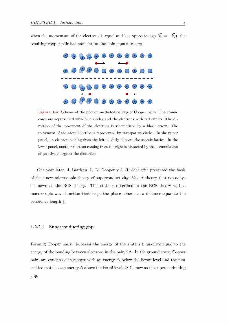
Figure 1.4: Scheme of the phonon mediated pairing of Cooper pairs. The atomic
cores are represented with blue circles and the electrons with red circles. The di-
rection of the movement of the electrons is schematized by a black arrow. The
movement of the atomic lattice is represented by transparent circles. In the upper
panel, an electron coming from the left, slightly distorts the atomic lattice. In the
lower panel, another electron coming from the right is attracted by the accumulation
of positive charge at the distortion.
One year later, J. Bardeen, L. N. Cooper y J. R. Schrieffer presented the basis
of their new microscopic theory of superconductivity [32]. A theory that nowadays
is known as the BCS theory. This state is described in the BCS theory with a
macroscopic wave function that keeps the phase coherence a distance equal to the
coherence length ξ.
1.2.2.1 Superconducting gap
Forming Cooper pairs, decreases the energy of the system a quantity equal to the
energy of the bonding between electrons in the pair, 2∆. In the ground state, Cooper
pairs are condensed in a state with an energy ∆ below the Fermi level and the first
excited state has an energy ∆ above the Fermi level. ∆ is know as the superconducting
gap.

CHAPTER 1. Introduction 9
1.3 Intermediate and Intermediate Mixed States
As it was presented before, below HC (Type I SC) or HC1 (Type II SC) no magnetic
field penetration is expected. Below this critical field, both types of superconductors
should behave as perfect diamagnets. But, some works have reported flux penetra-
tion below HC in type I SCs [36, 37] and below HC1 in type II SCs [19–21, 37–40].
This behaviour can be explained as a intermediate state (IS) in type I SCs and a
intermediate mixed state (IMS) in type II SCs.
1.3.1 Intermediate State
Figure 1.5: B-T phase diagram of a type I superconducting sphere. The curve
B=2/3BC(T ) separates the Meissner from the IS. The region where the IS takes
places is dashed.
Let us consider the case of a type I superconducting sphere (demagnetization
factor, N=1/3) in the presence of an external magnetic field in the Z direction. Below
TC , the magnetic field at the surface of the sphere is:
Bsurface = 32BasinΘ (1.15)
where Ba is the external magnetic field and Θ the polar angle in spherical coor-
dinates. If the external magnetic field is lower than 2/3BC , the surface field will be

CHAPTER 1. Introduction 10
Figure 1.6: Typical IS patterns in an In sample with thickness d= 10µ m for in-
creasing values of the applied magnetic field. Images a and b, correspond to h=0.105
and h=0.345, respectively (h=H/HC) at T = 1.85 K. SC domains are represented
in black and have circular or lamellar shapes. The edge of the sample is along the
right edge of the image. Adapted from [41]
lower than BC in all the surface, and the sphere will remain in the superconduct-
ing state. But, if the external magnetic field is greater than 2/3BC , from equation
1.15, there will be a range of angles where the surface field will exceed BC and the
sphere can not remain in the perfect superconducting state. In the range of external
magnetic fields:
23BC <Ba <BC (1.16)
The surface must decompose into superconducting and normal regions that keep
the internal field below the critical value HC in the superconducting regions at zero
and in the normal regions at Hc. This state is known as the intermediate state (IS).
The trigger of this state is the inhomogeneous distribution of the magnetic field on
the surface due to the demagnetization factor of the samples. A scheme of the phase
diagram for a superconducting sphere is shown in figure 1.5, where the dashed area
represents the region where the IS takes place. The IS was observed in various type
I superconductors in form of tongues or alternative domains of Meissner and normal
states [36, 37, 41] (figure 1.6).

CHAPTER 1. Introduction 11
Figure 1.7: Magnetic decoration of a square disk 5 × 5 × 1 mm3 of high pu-
rity polycrystalline Nb at 1.2 K and 1100 Oe, showing domains of Meissner and
mixed states. Magnetic flux penetrates from the edges in form of fingers which are
composed of vortex lattice. Adapted from [40].
1.3.2 Intermediate Mixed State
Following the same arguments than for type I SC, if a magnetic field is applied
to a type II superconductor, at certain fields below BC1, the SC will decompose
in domains in the Meissner state and domains in the mixed state, depending on
its demagnetization factor [37]. This regime is called the intermediate mixed state
(IMS). Experimentally it was found that the intervortex distance in the IMS domains
corresponds to the expected value corresponding to the inductance BC1 in equation
1.14. It was also found that the area occupied by the domains with zero induction
decreases linearly with the magnetic field, to reach BC1 when entering the mixed
phase [37]. An example of the IMS in a type II superconductor is presented in
figure 1.7 where the magnetic flux penetrates into the Nb forming domains in the
Meissner states and domains with a regular vortex lattice with a4 = 1.075√φ0/BC1,
independent of the magnetic field.
CHAPTER 1. Introduction 12
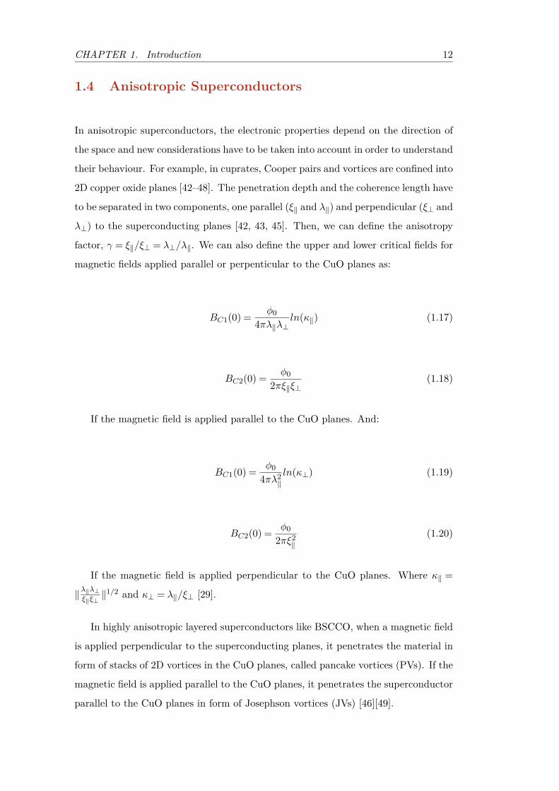
1.4 Anisotropic Superconductors
In anisotropic superconductors, the electronic properties depend on the direction of
the space and new considerations have to be taken into account in order to understand
their behaviour. For example, in cuprates, Cooper pairs and vortices are confined into
2D copper oxide planes [42–48]. The penetration depth and the coherence length have
to be separated in two components, one parallel (ξ‖ and λ‖) and perpendicular (ξ⊥ and
λ⊥) to the superconducting planes [42, 43, 45]. Then, we can define the anisotropy
factor, γ = ξ‖/ξ⊥ = λ⊥/λ‖. We can also define the upper and lower critical fields for
magnetic fields applied parallel or perpenticular to the CuO planes as:
BC1(0) = φ04πλ‖λ⊥
ln(κ‖) (1.17)
BC2(0) = φ02πξ‖ξ⊥
(1.18)
If the magnetic field is applied parallel to the CuO planes. And:
BC1(0) = φ04πλ2
‖ln(κ⊥) (1.19)
BC2(0) = φ02πξ2‖
(1.20)
If the magnetic field is applied perpendicular to the CuO planes. Where κ‖ =
‖λ‖λ⊥ξ‖ξ⊥‖1/2 and κ⊥ = λ‖/ξ⊥ [29].
In highly anisotropic layered superconductors like BSCCO, when a magnetic field
is applied perpendicular to the superconducting planes, it penetrates the material in
form of stacks of 2D vortices in the CuO planes, called pancake vortices (PVs). If the
magnetic field is applied parallel to the CuO planes, it penetrates the superconductor
parallel to the CuO planes in form of Josephson vortices (JVs) [46][49].

CHAPTER 1. Introduction 13
1.4.1 Pancake vortices
In BSCCO and other highly anisotropic superconductors, the CuO planes are sepa-
rated in the c-axis direction a distance s > ξ⊥ and therefore they act as Josephson
junctions [44–48]. A vortex perpendicular to these layers, which otherwise would
be considered a uniform cylinder of confined flux, is here a stacking of 2D pancake
shaped vortices (PVs), one PV per layer with surrounding currents confined to the
layer [42, 50–53]. PVs are so weakly coupled that thermal agitation can decouple
the stack of PVs [54]. A scheme of PVs in different layers of a highly anisotropic
superconductor is presented in figure 1.8.
Figure 1.8: Stack of 2D pancake vortices in a layered superconductor. Red circles
represents the 2D PVs while blue lines are a guide to the eye to connect the PVs at
different layers (grey planes).
1.4.2 Josephson vortices
In the case of an applied magnetic field parallel to the superconducting planes, the
field penetrates in highly anisotropic superconductors in form of Josephson vortices
(JVs) [48]. JVs do not have normal cores and their current distribution makes rather
wide loops between between two superconducting layers [46, 48]. The structure of the
core is similar to the structure of the phase drop across a flux line in two-dimensional
Josephson junctions, where the phase difference changes 2π between the two layers
over a distance of ΛJ [48]. For 3D superconductors, this length is given by ΛJ = γs,
and we can think of a central region of γs wide and s high as the core of the JV [48]
(figure 1.9). Beyond this core, the screening of the z-axis currents is weaker than by
in-plane currents, and the flux line is stretched into and ellipsoidal shape with a large

CHAPTER 1. Introduction 14
width (λ⊥) along the layers. A scheme of a JV is shown in figure 1.9.
Figure 1.9: Scheme of a JV in a layered superconductor with the in plane magnetic
field applied in the Y-direction. The Josephson vortex is also oriented along the Y-
direction. Horizontal blue lines represents the SC planes and the black arrows the
Josephson currents (vertical) and the supercurrents (horizontal) resulting from the
JV. The phase difference between the SC planes is summarized in the upper part of
the image. The phase difference changes 2π between the two layers over a distance
of ΛJ = γs, where γ is the anisotropy factor and s is the distance between CuO
planes.
Under an applied magnetic field parallel to the CuO planes, in the Y direction,
JVs arrange in a strongly stretched triangular lattice along the direction of the layers
with lattice parameters [48]:
az =√
2φ0/√
3γBy (1.21)
ax =√√
3γφ0/2By (1.22)
1.4.3 Crossing lattice
A huge variety of vortex configurations have been proposed when applying magnetic
field tilted with respect the c axis in highly anisotropic superconductors [44, 46, 47,
49, 55]. We will focus in the crossing lattices of PVs and JVs. In this configuration,
the JVs interact with the stacks of PVs splitting them in two branches giving a zig-zag
like structure perpendicular to the CuO planes [44, 46, 47, 49].
CHAPTER 1. Introduction 15
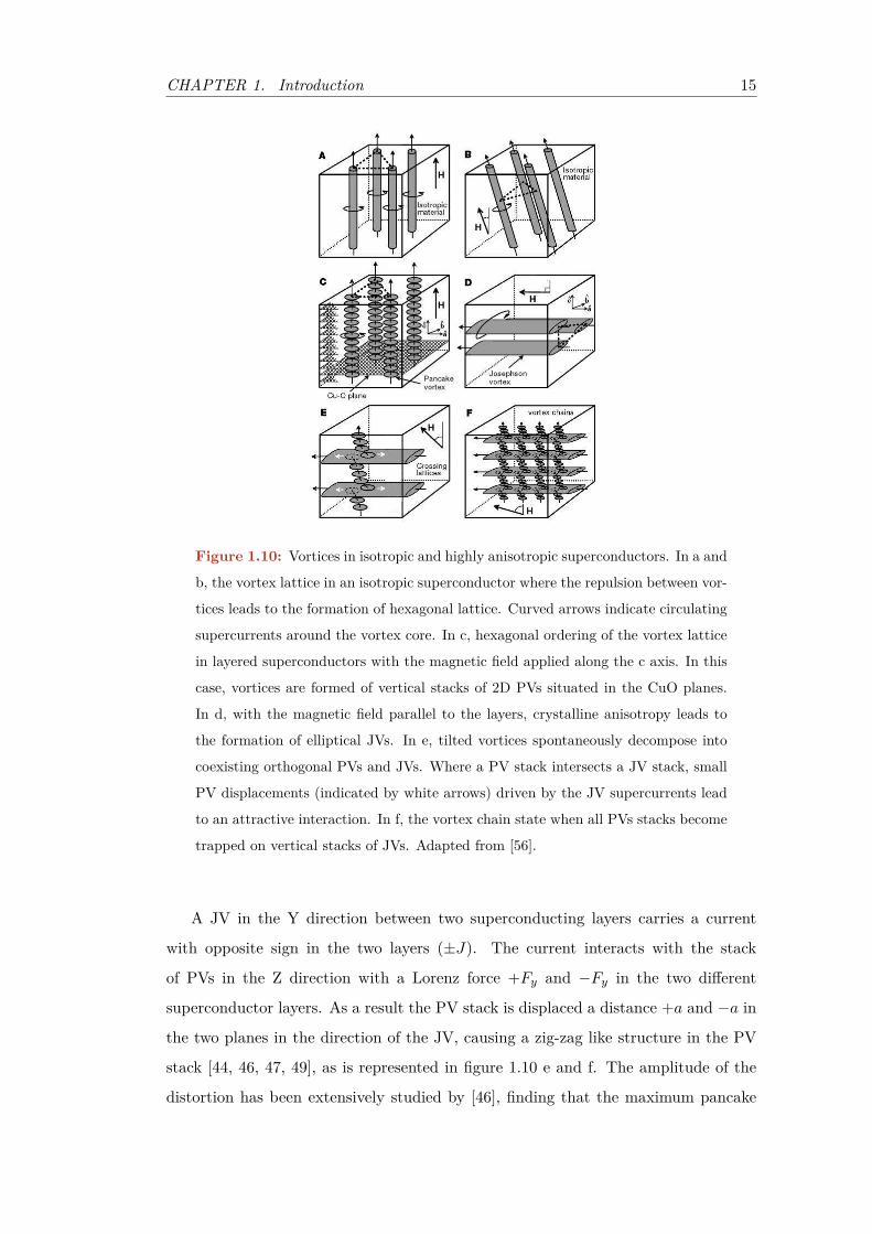
Figure 1.10: Vortices in isotropic and highly anisotropic superconductors. In a and
b, the vortex lattice in an isotropic superconductor where the repulsion between vor-
tices leads to the formation of hexagonal lattice. Curved arrows indicate circulating
supercurrents around the vortex core. In c, hexagonal ordering of the vortex lattice
in layered superconductors with the magnetic field applied along the c axis. In this
case, vortices are formed of vertical stacks of 2D PVs situated in the CuO planes.
In d, with the magnetic field parallel to the layers, crystalline anisotropy leads to
the formation of elliptical JVs. In e, tilted vortices spontaneously decompose into
coexisting orthogonal PVs and JVs. Where a PV stack intersects a JV stack, small
PV displacements (indicated by white arrows) driven by the JV supercurrents lead
to an attractive interaction. In f, the vortex chain state when all PVs stacks become
trapped on vertical stacks of JVs. Adapted from [56].
A JV in the Y direction between two superconducting layers carries a current
with opposite sign in the two layers (±J). The current interacts with the stack
of PVs in the Z direction with a Lorenz force +Fy and −Fy in the two different
superconductor layers. As a result the PV stack is displaced a distance +a and −a in
the two planes in the direction of the JV, causing a zig-zag like structure in the PV
stack [44, 46, 47, 49], as is represented in figure 1.10 e and f. The amplitude of the
distortion has been extensively studied by [46], finding that the maximum pancake

CHAPTER 1. Introduction 16
displacement at the JV core position is:
a≈2.2λ‖
γslog(2γs/λ‖)(1.23)
The distorted PV stack crossing a JV have less energy compared with other stacks,
which makes favourable to add an extra stack on top of the JV and form PV rows
along the JV [44] separated a distance[57]:
d≈ 2λ‖logB‖γ
2s2
φ0λ‖(1.24)
The existence of PVs rows decorating JVs have been confirmed in previous ex-
perimental works using scanning hall probe microscopy (note that this technique
is non-invasive, vortices can not be moved using a scanning hall probe microscope
[58–65]).
The crossing lattice of PVs and JVs causes a rearrangement of the phase distribu-
tion on the CuO planes and therefore in the JV structure. In an isolated JV in the Y
direction, the phase difference, ∆φ= φ1−φ0 ( φ1 and φ0 are the phases at both CuO
planes), between the top and bottom CuO planes changes by 2π over a distance ΛJin the X direction. The phase difference is 0 and 2π at the edges and π at the centre
of the JV (figure 1.11 b). Adding one PV in each layer, separated by an in-plane
distance 2a in the Y direction, causes a change in the phase in each CuO plane. The
phase changes by π between the extremes of the line that crosses a PV parallel to the
JV. The phase changes by π in both layers at different positions, creating a narrow
region, 2a width, where the phase difference between CuO layers is 2π instead of π
in the centre of the JV [46] (figure 1.11 c).
1.5 Iron Based Superconductors
Iron based superconductors (FeBSC) were first discovered by Kamihara et al. in
2006 [66]. They found that LaFePO transits to a superconducting state below 4 K.
CHAPTER 1. Introduction 17
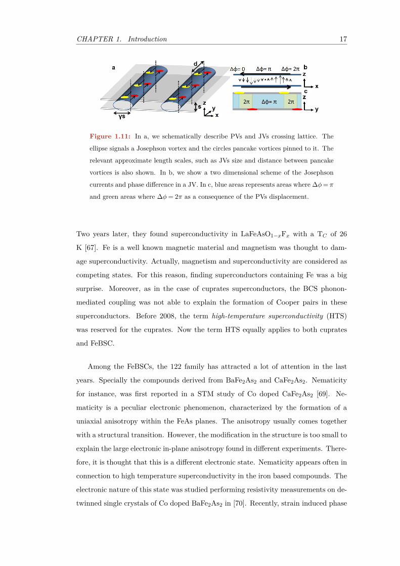
Figure 1.11: In a, we schematically describe PVs and JVs crossing lattice. The
ellipse signals a Josephson vortex and the circles pancake vortices pinned to it. The
relevant approximate length scales, such as JVs size and distance between pancake
vortices is also shown. In b, we show a two dimensional scheme of the Josephson
currents and phase difference in a JV. In c, blue areas represents areas where ∆φ= π
and green areas where ∆φ= 2π as a consequence of the PVs displacement.
Two years later, they found superconductivity in LaFeAsO1−xFx with a TC of 26
K [67]. Fe is a well known magnetic material and magnetism was thought to dam-
age superconductivity. Actually, magnetism and superconductivity are considered as
competing states. For this reason, finding superconductors containing Fe was a big
surprise. Moreover, as in the case of cuprates superconductors, the BCS phonon-
mediated coupling was not able to explain the formation of Cooper pairs in these
superconductors. Before 2008, the term high-temperature superconductivity (HTS)
was reserved for the cuprates. Now the term HTS equally applies to both cuprates
and FeBSC.
Among the FeBSCs, the 122 family has attracted a lot of attention in the last
years. Specially the compounds derived from BaFe2As2 and CaFe2As2. Nematicity
for instance, was first reported in a STM study of Co doped CaFe2As2 [69]. Ne-
maticity is a peculiar electronic phenomenon, characterized by the formation of a
uniaxial anisotropy within the FeAs planes. The anisotropy usually comes together
with a structural transition. However, the modification in the structure is too small to
explain the large electronic in-plane anisotropy found in different experiments. There-
fore, it is thought that this is a different electronic state. Nematicity appears often in
connection to high temperature superconductivity in the iron based compounds. The
electronic nature of this state was studied performing resistivity measurements on de-
twinned single crystals of Co doped BaFe2As2 in [70]. Recently, strain induced phase

CHAPTER 1. Introduction 18
Figure 1.12: In a, crystal structure of different families of iron pnictides. Fe-As
planes are highlighted as common features in all structures. In b, the FeAs plane
from a frontal (top) and upper (bottom) point of view. Spins are aligned ferro
and antiferromagnetic alternately in a structure called stripe like antiferromagnetic
order. Adapted from [68].
separation between superconducting tetragonal domains and non-superconducting
orthogonal domains was proposed in [71] in Co doped CaFe2As2.
FeBSC are also promising compounds to the study of superconductivity in the 2D
limit. In FeBSC, superconductivity has its origin in the 2D Fe-As layers, similar to
the CuO planes in the cuprates.
1.5.1 Phase diagram
FeBSC have 2D lattices of 3d transition metal ions as the building block, sitting
in a quasi-ionic framework composed of rare earth, oxygen, alkali or alkaline earth
blocking layers. They present phase diagrams with a magnetic ordered phase in the
parent compound and a superconducting dome developing with doping. They also
present orthorhombic transition at small doping.
Some compounds, for instance, LaFeAsO, shows first order transition between
magnetic and superconducting phases and in other compounds like the 122 family,
both states coexist for certain doping levels. FeBSC magnetic phases are metallic
with linear dependence of the resistivity with the temperature. They also show a

CHAPTER 1. Introduction 19
Figure 1.13: Generic temperature versus doping/pressure phase diagram for the
FeBSC. The parent compound usually presents a structural/magnetic transition
that reduces its temperature with increasing doping/pressure. The structural and
magnetic transitions are coupled or separated depending on the compound. Above
the structural transition and usually coupled to it and to the magnetic one there is
an electronic nematic phase. Superconductivity emerges in a dome-shape with finite
doping/pressure with the optimal doping usually coinciding with the extrapolation
of the magnetic phase to zero temperature. Adapted from [72].
structural phase transition which is often coupled with the magnetic transition. Above
them, the above mentioned nematic behavior has been reported in some compounds.
Superconductivity emerges as a dome at finite doping levels with the optimal doping
level located where the magnetic transition extrapolates to zero temperature. For
some materials there is a region where magnetism and superconductivity coexist. A
schematic representation of the generic phase diagram of FeBSC is presented in figure
1.13.
1.5.1.1 Electronic structure
The Fermi Surface (FS) of FeBSC is derived from the dxy, dyz and dxz orbitals of Fe
and the out of plane orbital of the As, with which Fe is in tetrahedral coordination
in a 2D layer (figure 1.12).
The electronic band structure has been calculated using the local density approx-
CHAPTER 1. Introduction 20
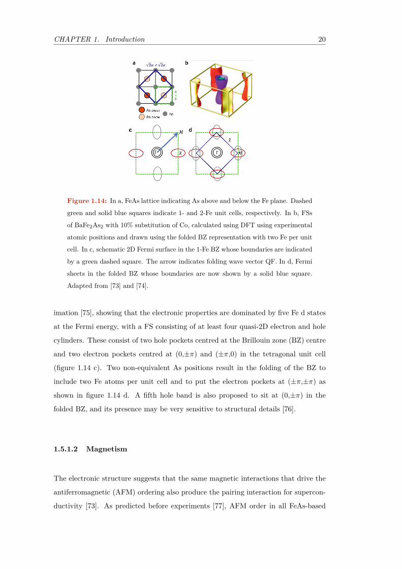
Figure 1.14: In a, FeAs lattice indicating As above and below the Fe plane. Dashed
green and solid blue squares indicate 1- and 2-Fe unit cells, respectively. In b, FSs
of BaFe2As2 with 10% substitution of Co, calculated using DFT using experimental
atomic positions and drawn using the folded BZ representation with two Fe per unit
cell. In c, schematic 2D Fermi surface in the 1-Fe BZ whose boundaries are indicated
by a green dashed square. The arrow indicates folding wave vector QF. In d, Fermi
sheets in the folded BZ whose boundaries are now shown by a solid blue square.
Adapted from [73] and [74].
imation [75], showing that the electronic properties are dominated by five Fe d states
at the Fermi energy, with a FS consisting of at least four quasi-2D electron and hole
cylinders. These consist of two hole pockets centred at the Brillouin zone (BZ) centre
and two electron pockets centred at (0,±π) and (±π,0) in the tetragonal unit cell
(figure 1.14 c). Two non-equivalent As positions result in the folding of the BZ to
include two Fe atoms per unit cell and to put the electron pockets at (±π,±π) as
shown in figure 1.14 d. A fifth hole band is also proposed to sit at (0,±π) in the
folded BZ, and its presence may be very sensitive to structural details [76].
1.5.1.2 Magnetism
The electronic structure suggests that the same magnetic interactions that drive the
antiferromagnetic (AFM) ordering also produce the pairing interaction for supercon-
ductivity [73]. As predicted before experiments [77], AFM order in all FeAs-based

CHAPTER 1. Introduction 21
superconducting systems is found to have a wave vector directed along (π,π) in the
tetragonal unit cell with a real-space spin arrangement consisting of AFM stripes
along one direction of the Fe sublattice and ferromagnetic stripes along the other
(figure 1.12).
It was predicted by DFT calculations [78] and confirmed by experiments [79] that
the magnetic ground state of FeTe has a double-stripe-type antiferromagnetic order in
which the magnetic moments are aligned ferromagnetically along a diagonal direction
and antiferromagnetically along the other diagonal direction of the Fe square lattice,
as shown schematically in figure 1.15 a. Meanwhile, DFT calculations predict that
the ground state of FeSe has the single-stripe-type antiferromagnetic order, similar
to those in LaFeAsO and BaFe2As2, as shown in figure 1.15 b.
Figure 1.15: In a, double-stripe-type antiferromagnetic order in FeTe. The solid
and hollow arrows represent two sublattices of spins. In b, single-stripe-type anti-
ferromagnetic order in BaFe2As2. The shaded area indicates the magnetic unit cell.
Adapted from [79]
The energetic stability of (π, 0) antiferromagnetic ordering over (π, π) ordering
in FeTe has been studied in [78]. They found that it can be described by the nearest,
second nearest, and third nearest neighbor exchange parameters, J1, J2, and J3,
respectively, with the condition J3 > J2/2. Authors in [80] found that Te height from
the Fe plane is a key factor that determines antiferromagnetic ordering patterns in
FeTe, so that the magnetic ordering changes from the (π, 0) with the optimized Te
height to the (π, π) patterns when Te height is lowered.
CHAPTER 1. Introduction 22
1.5.1.3 Superconducting gap
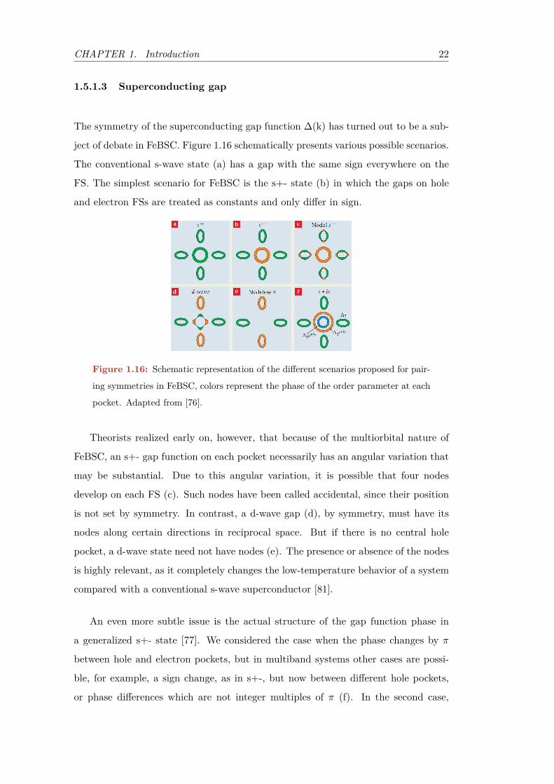
The symmetry of the superconducting gap function ∆(k) has turned out to be a sub-
ject of debate in FeBSC. Figure 1.16 schematically presents various possible scenarios.
The conventional s-wave state (a) has a gap with the same sign everywhere on the
FS. The simplest scenario for FeBSC is the s+- state (b) in which the gaps on hole
and electron FSs are treated as constants and only differ in sign.
Figure 1.16: Schematic representation of the different scenarios proposed for pair-
ing symmetries in FeBSC, colors represent the phase of the order parameter at each
pocket. Adapted from [76].
Theorists realized early on, however, that because of the multiorbital nature of
FeBSC, an s+- gap function on each pocket necessarily has an angular variation that
may be substantial. Due to this angular variation, it is possible that four nodes
develop on each FS (c). Such nodes have been called accidental, since their position
is not set by symmetry. In contrast, a d-wave gap (d), by symmetry, must have its
nodes along certain directions in reciprocal space. But if there is no central hole
pocket, a d-wave state need not have nodes (e). The presence or absence of the nodes
is highly relevant, as it completely changes the low-temperature behavior of a system
compared with a conventional s-wave superconductor [81].
An even more subtle issue is the actual structure of the gap function phase in
a generalized s+- state [77]. We considered the case when the phase changes by π
between hole and electron pockets, but in multiband systems other cases are possi-
ble, for example, a sign change, as in s+-, but now between different hole pockets,
or phase differences which are not integer multiples of π (f). In the second case,
CHAPTER 1. Introduction 23
superconducting order breaks time-reversal symmetry and is therefore dubbed s + is.
1.6 Induced superconductivity in 2D systems
Superconductivity induced in low dimensional systems attracts considerable interest
of both theorists and experimentalists for many decades. Recently, one sees a revival
of this interest in connection with the growing number of experiments carried out
for a variety of new artificial systems which include two-dimensional electron gas,
graphene, semiconducting nanowires and carbon nanotubes, topological insulators,
etc [82, 83].
Authors in [84] have studied the problem of induced superconductivity in a nor-
mal thin layer in contact with a superconductor in detail. They considered several
fundamental properties of the vortex matter in the systems with induced supercon-
ducting order. They argued that the proximity induced superconducting gap ∆2D
is responsible for appearance of a new length scale in the vortex structure, the 2D
coherence length, ξ2D = hv2F /∆2D; ξ2D=√hD2D/∆2D for clean or dirty limits, re-
spectively. Here v2F and D2D are the Fermi velocity and diffusion constant in the 2D
layer. The energy gap ∆2D depends on the tunneling rate Γ ; for example, ∆2D ≈ Γ
for Γ << ∆. The 2D penetration depth λ2D ∝ 1/∆22D increases as ∆2D decreases.
Therefore, a higher penetration depth is expected in the induced superconductor and
a change in the local screening properties may be measurable on it using MFM, Hall
microscopy or other local magnetic measurements.
1.6.1 Induced superconductivity on graphene
Graphene is a bidimensional material consisting in C atoms arranged in honeycomb
arrangement. The electronic structure of an isolated C atom is (1s)2 (2s)2 (2p)4. The
1s electrons remain within the isotropic s-configuration, but the 2s and 2p electrons
hybridize. One possible result is four sp3 orbitals, which naturally tend to establish
a tetrahedral bonding pattern. This is what happens in diamond. However, an
alternative possibility is to form three sp2 orbitals, leaving over a more or less pure p-

CHAPTER 1. Introduction 24
orbital. In that case the natural tendency is for the sp2 orbitals to arrange themselves
in a plane at 120 angles like in the case of graphene (figure 1.17).
A calculation of graphene’s band structure as early as 1947 captured the dynamics
of its electrons in the crystal lattice [85]. Now, 60 years later, Geim and his collabo-
rators [86], and separately a team from Columbia University led by Philip Kim [87],
have experimentally explored the nature of graphene’s conductivity and verified the
exotic electrical properties. In particular, that its mobile electrons behave as if they
were massless, relativistic fermions. In conventional semiconductors, electrons are as-
cribed an effective mass m∗ that accounts for their interaction with the lattice. The
energy E depends quadratically on the momentum (E = h~k2/2m∗, where k is the
electron wavevector).
Figure 1.17: Graphene honeycomb lattice and its Brillouin zone. In the left panel,
lattice structure of graphene, composed of two interpenetrating triangular lattices
represented by red and blue circles ( ~a1 and ~a2 are the lattice unit vectors of the
lattice). In the right panel, the corresponding Brillouin zone.
Graphite, a semimetal whose bands slightly overlap and allow pockets of electrons
and holes to tunnel between layers, confirm such a dispersion relation. But in a single
graphene sheet, the overlap shrinks down to a single point (Dirac point), where the
bands barely touch (see figure 1.18). The result is perfect symmetry between a band
filled with holes and a band filled with electrons. More significantly, the dispersion
of those bands is linear as they approach each other. Consequently, the electron
dynamics are best modeled by a relativistic Dirac equation, which describes a linear
relation between energy and momentum: E = h~kvF , in which the Fermi velocity vFof electrons or holes replaces the speed of light. The dispersion curve then implies

CHAPTER 1. Introduction 25
that the electrons mass vanishes throughout a large range of momentum values in the
crystal lattice.
Figure 1.18: Band structure of graphene. In the left panel, the band structure
of a single graphene layer along MΓKM. The inset is an enlargement of the region
indicated by the square around the K point. In the right panel, a band-structure
picture of the crystal describes the energy dependence of that electronic motion. A
semimetal, graphene has valence and conduction bands that just touch at discrete
points in the Brillouin zone. The energy-momentum dispersion relation becomes
linear in the vicinity of those points, with the dispersion described by the relativistic
energy equation E = h~kvF , where vF is the Fermi velocity and ~k its momentum.
Consequently, an electron has an effective mass of zero and behaves more like a
photon than a conventional massive particle whose energy-momentum dispersion is
parabolic. Adapted form [88] and [89]
Electrons in single-layer graphene (SLG) are predicted to condense to a super-
conducting state, either intrinsically by doping [78, 90–95] or by placing SLG on a
superconductor with a BCS or a non-BCS pairing symmetry [96, 97]. The resulting
symmetry depends on the position of the Fermi energy (EF ) with respect to the Dirac
point. In particular, for FE shifts up to 1 eV, a p-wave [78, 92] state is predicted.
As the doping approaches the van Hove singularity (FE ≈ 3 eV; ref. [95]), a sin-
glet chiral d-wave and triplet f-wave symmetry are also predicted [93, 96]. Ref. [94]
found dominant chiral d-wave superconductivity near van Hove doping and argued
that weak coupling superconductivity for doping levels between half-filling and the
van Hove density is of Kohn-Luttinger type and likely to be f-wave pairing for discon-
nected Fermi pockets. Reference [92] predicted that a non-chiral p-wave symmetry is
favoured for small nearest-neighbour repulsion (<1.1 eV), small onsite interaction U
(≈ 8.4 eV) or large doping (above 10%), whereas the chiral p-wave state occurs as U

CHAPTER 1. Introduction 26
or V are increased or the doping level diminishes with respect to the aforementioned
values (in pure SLG at half-filling U is ≈ 9.3 eV and V is 5.5 eV; ref. [92]). At low
density (20%) and including next-nearest neighbour hopping, a chiral p-wave state
can emerge [78]. Moreover, the possibility of spin-triplet s-wave pairing has been
considered in bilayer graphene [98].
Although intrinsic superconductivity in SLG has not been observed [99], super-
conductivity has been induced by doping SLG with Li adatoms [100], intercalating
SLG sheets with Ca (ref. [101]) or by placing SLG on a superconductor [102]. In the
latter case, the intrinsic pairing potential for p- or chiral d-wave superconductivity can
be in principle, as shown by calculations, [97, 103] to the point that a full transition
to a superconducting state is triggered and manifested in the SLG superconducting
density of states (DoS).
Tonnoir et al. [102] locally probed the superconducting DOS in SLG on the s-wave
superconductor Re by scanning tunnelling microscopy (STM). They found induced
superconductivity in SLG from the observation of a gapped DOS that matched the
underlying layer of Re (s-wave). The absence of unconventional superconductivity,
may indicate a modification of the SLG band structure [104, 105] due to the high
carrier density of Re (ne ≈4.5 × 1023 cm−3) resulting in significant charge transfer.
1.7 Motivation
The vortex distribution has been studied in a huge amount of superconducting sys-
tems like type I, BCS prototype type II or High TC superconductors. The knowledge
of their interaction and distribution has remarkably advanced in the last decades.
But, there are still open questions on this matter. For example, the study of the vor-
tex distribution is usually made on the mixed state of type II SCs at magnetic fields
well above HC1. Some works have advanced in the understanding of the IMS in type
II SCs, but the mechanism of formation of vortex patterns below HC1 is still an open
debate [19–21]. In particular, the possible mechanisms of the vortex distributions
at very low fields and the current controversies on this matter are discussed exten-

CHAPTER 1. Introduction 27
sively in [40]. Moreover, the majority of the previous works have been focused on the
“passive” characterization of the vortex lattice but not on its local manipulation with
scanning techniques. Some recent works have successfully manipulated Abrikosov
vortices in 3D superconductors [106–109] but the manipulation of 2D pancake vor-
tices and Josephson vortices in highly anisotropic systems has not been achieved yet.
In particular, the force exerted on a PV by a JV has not been measured yet. On the
other hand, the coexistence between superconductivity and magnetism has attracted
a lot of attention in the last decade. Several theoretical and experimental attempts to
understand the interplay between both states have been done in the last years. But,
the interplay of the magnetism in the superconducting state and the paring mech-
anism of the Copper pairs in these systems remains unclear [68, 73, 77, 110–112].
In addition, the local characterization of a system where magnetic and supercon-
ducting domains coexist has not been achieved yet. The recent proposal of phase
separation between superconducting and antiferromagnetic domains under the action
of biaxial strain in Co doped CaFe2As2, opens a good opportunity to perform the
local characterization of this coexistence [71]. Finally, induced superconductivity in
graphene is one of the great goals of the last few years. Several groups have reported
insight of superconducting behavior in graphene by different techniques. But, there
is no microscopic evidence of the magnetic properties of graphene in contact with a
superconductor.
From an experimental point of view, answering those question needs a scanning
probe technique capable to measures the topographic and magnetic profiles in areas of
several tens of microns at low temperatures in a short period of time. Tilted magnetic
fields are useful to study in-plane anisotropies or to determine the direction of, for
instance, Josephson vortices. In order to manipulate the superconducting vortices in
a controlled way, the scanning technique also has to be able to interact with them
when necessary and avoid perturbations when not desired. For these reasons, during
the thesis, a set-up with a magnetic force microscope of low temperatures working in
combination with a homemade three axis superconducting magnetic coil was employed
as the main technique. The magnetic force microscopy is the only technique that
allows to measure simultaneously the topography and the local magnetic profile of
samples. In addition MFM has probed to be an effective tool to local manipulation

CHAPTER 1. Introduction 28
of magnetic structures.
Our set-up has allowed us to characterize areas up to 20×20 µm2 at low tempera-
tures in a few minutes with tilted applied magnetic fields and interact with magnetic
structures on the samples in a controlled way. Four systems were selected in the thesis
due to their specifics properties to try to bring some light in the topics we have pre-
sented in the previous paragraphs, β-Bi2Pd, Bi2Sr2CaCu2O8, Ca(Fe0.965Co0.35)2As2and different β-Bi2Pd/graphene heterostructures.

CHAPTER 2
Experimental methods
In this thesis, I have used magnetic force microscopy (MFM) at low temperatures to
investigate the local properties of several superconductors. MFM allows to measure
the magnetic field distribution at low temperatures in large areas (20 × 20 µm2 at 2
K in our case) in rough or nanostructured samples where the differences in height are
too big for techniques like scanning tunnelling microscopy (STM). MFM also allows
single vortex manipulation [113]. For these reasons, MFM has become one of the
most interesting techniques to study the local magnetism in different systems.
This chapter has been organized in three sections. The first one is devoted to the
description of our experimental set-up. The second section collects a detailed charac-
terization of the MFM probes at low temperature. Finally, the third section describes
the solution growth method used to grow several of the crystals characterized in this
work
2.1 Set-up
A Low Temperature Atomic Force Microscope (LT-AFM) from Nanomagnetics In-
struments Ltd. was employed during the thesis. It was used to characterize the super-
conducting vortex lattice and magnetic domains of several samples using the MFM
mode. The microscope was used in combination with a home-designed cryostat and a
29
CHAPTER 2. Experimental methods 30
commercial variable temperature insert (VTI) provided by American Magnetics Inc.
and a home-made three axis magnetic vector magnet.
2.1.1 Cryostat, VTI and vibration isolation stage
Our cryostat consists of a 80 L liquid He main chamber where the VTI and the
superconducting coil are placed. To isolate the liquid He bath from room temperature,
the chamber is covered on top by a 50 L liquid nitrogen bath and both chambers
are surrounded by a high vacuum compartment separated by stainless steel walls.
The isolation of the liquid He bath allows us to perform experiments down to 2 K
for a couple of days without refilling the cryostat. The system is designed to fit a
commercial VTI and a home-made magnet inside. An scheme of the cryostat is shown
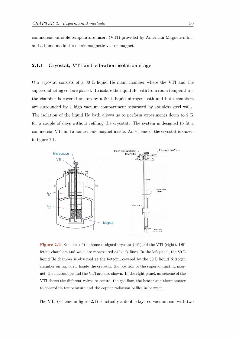
in figure 2.1.
Figure 2.1: Schemes of the home-designed cryostat (left)and the VTI (right). Dif-
ferent chambers and walls are represented as black lines. In the left panel, the 80 L
liquid He chamber is observed at the bottom, covered by the 50 L liquid Nitrogen
chamber on top of it. Inside the cryostat, the position of the superconducting mag-
net, the microscope and the VTI are also shown. In the right panel, an scheme of the
VTI shows the different valves to control the gas flow, the heater and thermometer
to control its temperature and the copper radiation baffles in between.
The VTI (scheme in figure 2.1) is actually a double-layered vacuum can with two
CHAPTER 2. Experimental methods 31
spaces in between. It is designed to fit inside the magnetic coil in the He chamber. The
inner space of the VTI is designed to accommodate our LT-AFM inside. To perform
the measurements, the inner space is pumped to high vacuum and then filled with
helium gas to a desired pressure (typically 0.5 atmospheres) to control the thermal
contact between the liquid He bath and the microscope. The operating principle can
be briefly described as follows. Through a narrow capillary, the helium liquid from
the bath is siphoned into the outer space of the VTI, controlled by a needle valve.
Meanwhile, the gaseous helium is pumped out through a mechanical pump. Thus,
the cooling power is generated by the evaporation process of liquid helium and cold
gas flowing through the outer space.
There are two working modes for the VTI, that is, one-shot mode and continuous-
flow mode. In one-shot mode, the needle valve is fully opened for a while, and a
large amount of liquid helium is transferred into the outer space. Then, the needle
valve is totally closed and no liquid comes in. Through sustained pumping, the base
temperature can be achieved with a typical value of 1.3 K, which depends on the
heat load and pumping speed. In continuous-flow mode, the needle valve is kept open
at a position and the liquid helium flows into the VTI continuously. As the gaseous
helium is pumped out, a wide range of temperatures can be stabilized by controlling
the temperature of the He gas with a 50 Ω heater on the bottom of the VTI. The
heater response is fixed by a commercial Cryocon Temperature controller. The VTI
provides excellent thermal response with greater sample thermal stability allowing to
a perfect control of the temperature at the microscope during the experiments with
oscillations below 0.01 K. The cryostat is placed on a vibration isolation system.
The He evaporated and pumped out from the cryostat is heated and directed
to a recovery line to liquefy it again at the Servicios de Apoyo a la Investigacion
Experimental (SEGAINVEX) facilities.
In figure 2.2, a picture of the cryostat, the isolation stage, the mechanical pump,
the heaters, the recovery line and the control electronics is presented.

CHAPTER 2. Experimental methods 32
Figure 2.2: Picture of our set-up at the laboratory. In the image are shown the
electronics to control the superconducting magnet (a), the temperature controller
(b), the mechanical pump used to control the gas flow in the VTI (c), the isolation
stage (d), the cryostat (e), the heaters to warm the cold He pumped from the VTI
(f), the He recovery line (g) and the electronics of the LT-AFM (h).
2.1.2 Three axis superconducting vector magnet
A three axis homemade superconducting vector magnet is placed inside the cryostat,
in the liquid He bath. The magnet design is presented in reference [114] and consists
of five superconducting coils made of NbTi wire, one coil for z axis field and two sets
of split coils for the xy-plane field. The five coils are mounted in an Al cage. In figure
2.3 a and b, an scheme and a real picture of the coil are presented.
The magnet allows us to generate a magnetic field in any direction of the space
up to fields of 5 T in the Z direction and 1.2 T in the X and Y direction, using a
current of about 100 A. We have measured the magnetic field as a function of the
distance and find a homogeneous field within a sphere around the center of the coil
system of 0.2% for the magnetic field along the z axis, and of 1% for the magnetic
field in the plane (Fig2.3 c). The three coil system is equipped with persistent mode
switches for each set of coils giving, x, y and z components of the magnetic field. This
allows us to keep a constant magnetic field over long periods of time. The magnet is
energized using a power supply with three independent current sources, each one has
a commuted internal commercial stage of 5 V 100 A, followed by a voltage to current

CHAPTER 2. Experimental methods 33
Figure 2.3: In a, an scheme of our home-made three axis vector magnet. The
superconducting coils are represented in orange and the Al cage in yellow. One long
coil is used to generate the z-axis magnetic field. For the in-plane field, we use two
crossed split coil systems centred on the z-axis coil. The three directions of the
space, X, Y and Z are marked with black arrows on the scheme of the coils, together
with the real dimensions. In b, a real picture of the vector magnet. In c, we show
the magnetic field vs z-axis position, with respect to the centre of the magnet when
the z-coil is energized (50 A) (main panel) and when the x or y coils are energized
(75 A, inset). Red line is a guide to the eye.
Figure 2.4: In a, we show a scheme of the current power supply for the magnet.
In b, we show a photograph of the power supply. It is rather compact, 50 cm high
and 80 cm long.
converter consisting of a stage providing linear regulation which uses MOSFET power
transistors. Figure 2.4 shows an scheme of the circuits and a photograph of the power
supply. The power supply was designed and made at SEGAINVEX mostly by M.
Cuenca.
2.1.3 Low Temperature Microscope
The LT-AFM can be divided in two main parts, the insert and the head. The insert
can be attached to the microscope head using low temperature connectors, allowing
the exchange of different heads such as AFM, SHPM, STM etc. Radiation buffers are

CHAPTER 2. Experimental methods 34
placed along a stainless steel tube that gives mechanical shielding and guide to all
the necessary wires. It has a KF 40/50 connector on the top that fits in the variable
temperature insert (VTI) space of the cryostat. A schematic representation of the
microscope is presented in figure 2.5.
Figure 2.5: Scheme of the LT-AFM microscope. In the picture the whole micro-
scope, insert and head, is shown. At the top of the microscope, the KF-40 neck that
fits on the VTI. In the middle, the docking station to attach the insert to different
microscope heads. At the bottom, the AFM head, the outer piezo, the quartz tube
and the sample holder are shown.
The microscope head is formed by the AFM probe holder, two concentric lead
zirconate piezotubes, a quartz tube, and the sample holder. A real picture of the
LT-AFM head is shown in figure 2.6).
2.1.3.1 AFM probe holder
The AFM probe holder is attached to the inner piezotube by two screws. It has a
commercial AFM alignment holder from NanoSensors, glued on top of a small piezo
stack element, which is sandwiched between two alumina plates. The AFM probe is
fixed on the AFM holder using a spring connected to the body of the holder. The
AFM holder also has a Zirconium ferrule tube used to align the end of an optical fibre
with respect the AFM probe. The optical fibre is used to control the cantilever dis-
placement with the so-called optical laser interferometer method (see section 2.1.3.5).
The piezo below the alignment holder is used to control the fibre-probe distance. A
schematic representation of the AFM probe holder is presented in figure 2.7.

CHAPTER 2. Experimental methods 35
Figure 2.6: Real picture of the head of the LT-AFM. It shows the piezo holders,
the two piezo tubes (wrapped in Teflon in the picture), the quartz tube and the
AFM probe holder.
Figure 2.7: In the left panel, an scheme of the AFM probe holder. The body of the
holder is represented in blue. The ferrule tube is shown in black, the AFM probe
in yellow, the AFM alignment holder in brown, the piezo in grey and the spring in
orange. In the right panel, a picture zoomed in the ferrule tube and the probe.

CHAPTER 2. Experimental methods 36
2.1.3.2 Sample holder
The sample holder is a hollow cylinder made of Phosphor bronze with a hole at the
top that fits in the quartz tube. At the bottom, it has a plate where the sample is
glued and a connector to bias the sample. At the side, it has a leaf spring used to
attach it to the quartz tube. A picture of the sample holder is presented in figure 2.8.
Figure 2.8: Real picture of the sample holder. In the image are visible, the leaf
spring used to attach the sample slider to the quartz tube, the plate where the
sample is glued and the bias connector.
2.1.3.3 Scanning and tip oscillation system
The inner piezotube is used to oscillate and scan the AFM probe over the samples. It
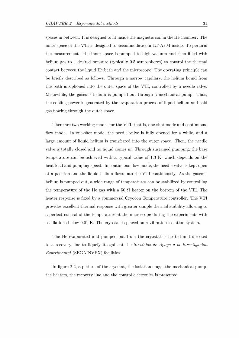
has quadrant electrodes and a circular electrode at its apex as is schematized in figure
2.9. If an opposite voltage is applied to reciprocal electrodes, the tube will bend as is
shown in figure 2.9 a. On the other hand if the same voltage is applied to all quadrant
electrodes with respect to the inner electrode, the tube will extend or contract in the
Z direction. It has a ≈ 20µm scan range in the XY plane and a ≈ 1.5µm retract range
in the Z direction at 2 K applying a voltage difference of 200 V between electrodes.
The single electrode at its apex is used to oscillate the AFM probe by applying and
oscillating difference of potential to the electrode as is schematized in 2.9 c.
2.1.3.4 Approaching-retracting mechanism
The outer piezotube and the quartz tube are used to perform the approaching and
retracting movement of the sample with respect to the AFM probe using the so-called
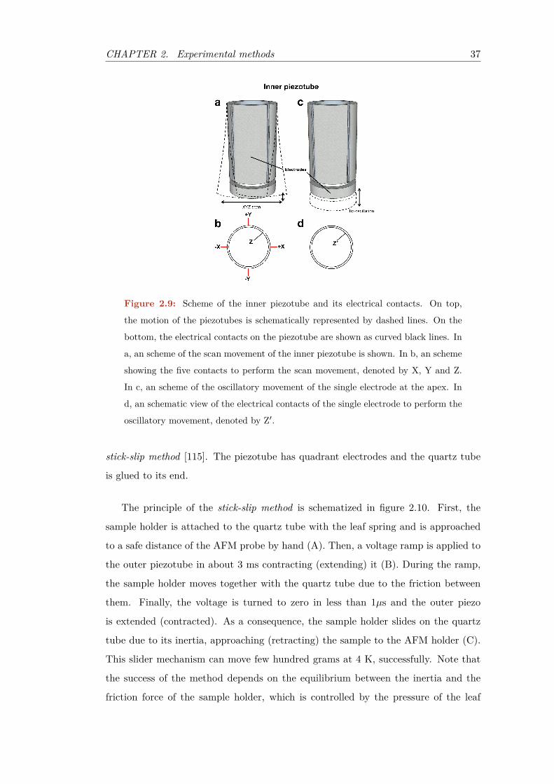
CHAPTER 2. Experimental methods 37
Figure 2.9: Scheme of the inner piezotube and its electrical contacts. On top,
the motion of the piezotubes is schematically represented by dashed lines. On the
bottom, the electrical contacts on the piezotube are shown as curved black lines. In
a, an scheme of the scan movement of the inner piezotube is shown. In b, an scheme
showing the five contacts to perform the scan movement, denoted by X, Y and Z.
In c, an scheme of the oscillatory movement of the single electrode at the apex. In
d, an schematic view of the electrical contacts of the single electrode to perform the
oscillatory movement, denoted by Z′.
stick-slip method [115]. The piezotube has quadrant electrodes and the quartz tube
is glued to its end.
The principle of the stick-slip method is schematized in figure 2.10. First, the
sample holder is attached to the quartz tube with the leaf spring and is approached
to a safe distance of the AFM probe by hand (A). Then, a voltage ramp is applied to
the outer piezotube in about 3 ms contracting (extending) it (B). During the ramp,
the sample holder moves together with the quartz tube due to the friction between
them. Finally, the voltage is turned to zero in less than 1µs and the outer piezo
is extended (contracted). As a consequence, the sample holder slides on the quartz
tube due to its inertia, approaching (retracting) the sample to the AFM holder (C).
This slider mechanism can move few hundred grams at 4 K, successfully. Note that
the success of the method depends on the equilibrium between the inertia and the
friction force of the sample holder, which is controlled by the pressure of the leaf
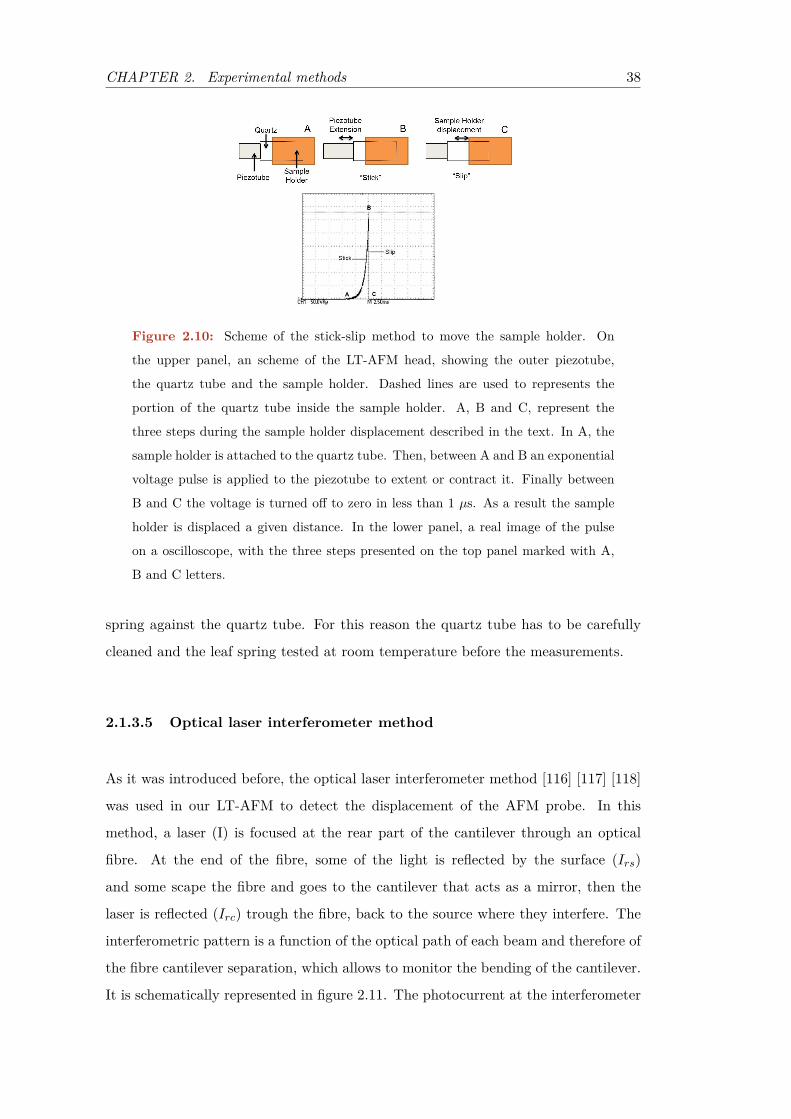
CHAPTER 2. Experimental methods 38
Figure 2.10: Scheme of the stick-slip method to move the sample holder. On
the upper panel, an scheme of the LT-AFM head, showing the outer piezotube,
the quartz tube and the sample holder. Dashed lines are used to represents the
portion of the quartz tube inside the sample holder. A, B and C, represent the
three steps during the sample holder displacement described in the text. In A, the
sample holder is attached to the quartz tube. Then, between A and B an exponential
voltage pulse is applied to the piezotube to extent or contract it. Finally between
B and C the voltage is turned off to zero in less than 1 µs. As a result the sample
holder is displaced a given distance. In the lower panel, a real image of the pulse
on a oscilloscope, with the three steps presented on the top panel marked with A,
B and C letters.
spring against the quartz tube. For this reason the quartz tube has to be carefully
cleaned and the leaf spring tested at room temperature before the measurements.
2.1.3.5 Optical laser interferometer method
As it was introduced before, the optical laser interferometer method [116] [117] [118]
was used in our LT-AFM to detect the displacement of the AFM probe. In this
method, a laser (I) is focused at the rear part of the cantilever through an optical
fibre. At the end of the fibre, some of the light is reflected by the surface (Irs)
and some scape the fibre and goes to the cantilever that acts as a mirror, then the
laser is reflected (Irc) trough the fibre, back to the source where they interfere. The
interferometric pattern is a function of the optical path of each beam and therefore of
the fibre cantilever separation, which allows to monitor the bending of the cantilever.
It is schematically represented in figure 2.11. The photocurrent at the interferometer
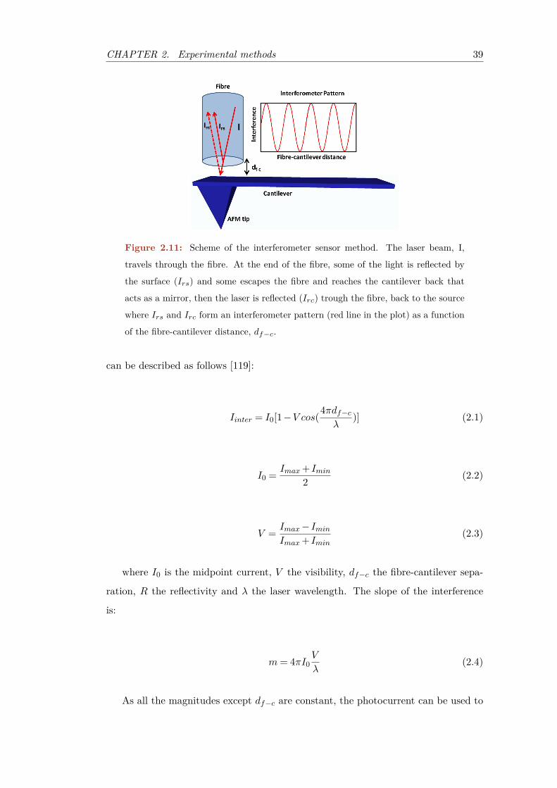
CHAPTER 2. Experimental methods 39
Figure 2.11: Scheme of the interferometer sensor method. The laser beam, I,
travels through the fibre. At the end of the fibre, some of the light is reflected by
the surface (Irs) and some escapes the fibre and reaches the cantilever back that
acts as a mirror, then the laser is reflected (Irc) trough the fibre, back to the source
where Irs and Irc form an interferometer pattern (red line in the plot) as a function
of the fibre-cantilever distance, df−c.
can be described as follows [119]:
Iinter = I0[1−V cos(4πdf−cλ
)] (2.1)
I0 = Imax+ Imin2 (2.2)
V = Imax− IminImax+ Imin
(2.3)
where I0 is the midpoint current, V the visibility, df−c the fibre-cantilever sepa-
ration, R the reflectivity and λ the laser wavelength. The slope of the interference
is:
m= 4πI0V
λ(2.4)
As all the magnitudes except df−c are constant, the photocurrent can be used to
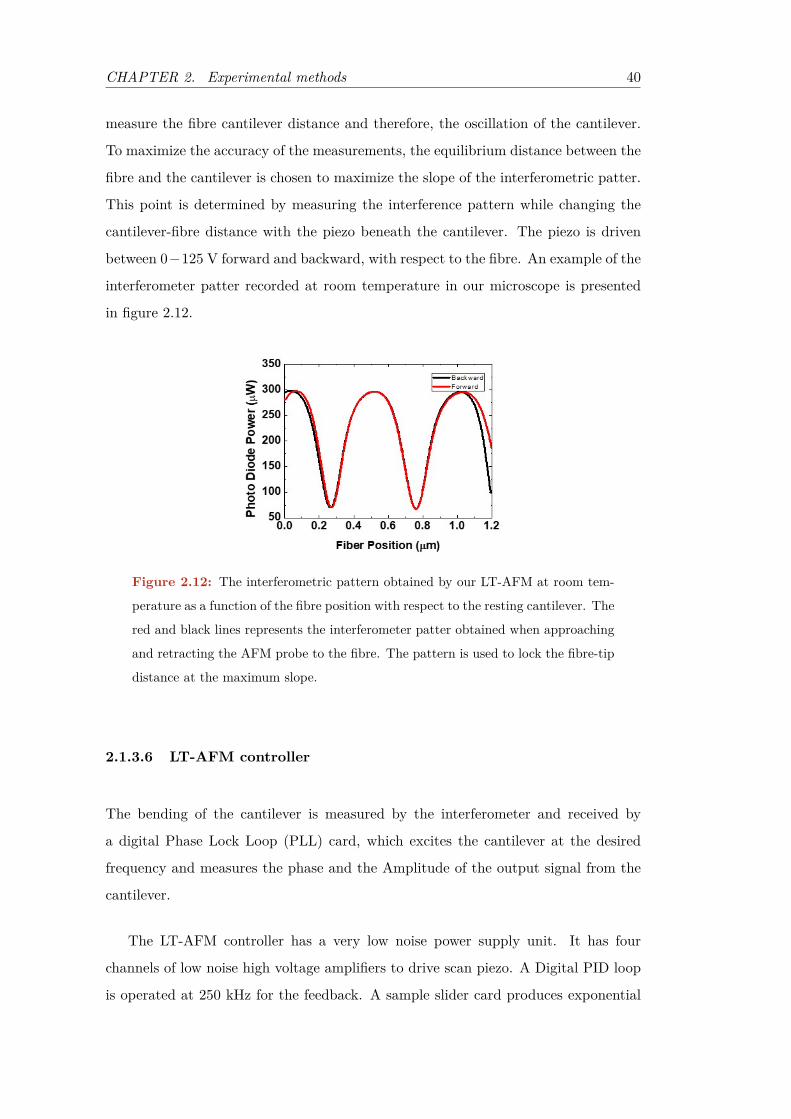
CHAPTER 2. Experimental methods 40
measure the fibre cantilever distance and therefore, the oscillation of the cantilever.
To maximize the accuracy of the measurements, the equilibrium distance between the
fibre and the cantilever is chosen to maximize the slope of the interferometric patter.
This point is determined by measuring the interference pattern while changing the
cantilever-fibre distance with the piezo beneath the cantilever. The piezo is driven
between 0−125 V forward and backward, with respect to the fibre. An example of the
interferometer patter recorded at room temperature in our microscope is presented
in figure 2.12.
Figure 2.12: The interferometric pattern obtained by our LT-AFM at room tem-
perature as a function of the fibre position with respect to the resting cantilever. The
red and black lines represents the interferometer patter obtained when approaching
and retracting the AFM probe to the fibre. The pattern is used to lock the fibre-tip
distance at the maximum slope.
2.1.3.6 LT-AFM controller
The bending of the cantilever is measured by the interferometer and received by
a digital Phase Lock Loop (PLL) card, which excites the cantilever at the desired
frequency and measures the phase and the Amplitude of the output signal from the
cantilever.
The LT-AFM controller has a very low noise power supply unit. It has four
channels of low noise high voltage amplifiers to drive scan piezo. A Digital PID loop
is operated at 250 kHz for the feedback. A sample slider card produces exponential
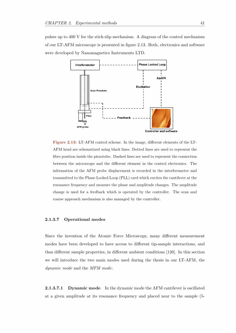
CHAPTER 2. Experimental methods 41
pulses up to 400 V for the stick-slip mechanism. A diagram of the control mechanism
of our LT-AFM microscope is presented in figure 2.13. Both, electronics and software
were developed by Nanomagnetics Instruments LTD.
Figure 2.13: LT-AFM control scheme. In the image, different elements of the LT-
AFM head are schematized using black lines. Dotted lines are used to represent the
fibre position inside the piezotube. Dashed lines are used to represent the connection
between the microscope and the different element in the control electronics. The
information of the AFM probe displacement is recorded in the interferometer and
transmitted to the Phase Locked Loop (PLL) card which excites the cantilever at the
resonance frequency and measure the phase and amplitude changes. The amplitude
change is used for a feedback which is operated by the controller. The scan and
coarse approach mechanism is also managed by the controller.
2.1.3.7 Operational modes
Since the invention of the Atomic Force Microscopy, many different measurement
modes have been developed to have access to different tip-sample interactions, and
thus different sample properties, in different ambient conditions [120]. In this section
we will introduce the two main modes used during the thesis in our LT-AFM, the
dynamic mode and the MFM mode:
2.1.3.7.1 Dynamic mode In the dynamic mode the AFM cantilever is oscillated
at a given amplitude at its resonance frequency and placed near to the sample (5-

CHAPTER 2. Experimental methods 42
15nm). In such scenario, the tip is near enough to the surface to interact via short
range Van der Waals (VdW) forces with the surface [120, 121]. The oscillation am-
plitude should be large enough to ensure that the restoring force at the lower turning
point is larger than the attractive force between tip and sample. This will avoid an
instability, which would stop or at least seriously distort the oscillation. The tip-
sample interaction causes a shift in the resonance frequency which is used to measure
the force acting on the tip [120, 121].
If we approximate the cantilever and the tip as point-mass spring (figure 2.14),
we can consider the AFM probe as a damped oscillator due to friction forces, with
some driving force, and into a force field created by the tip sample interaction, then
its movement can be described by a linear, second-order differential equation [120]:
Figure 2.14: Point-like mass spring as an approximation of the AFM cantilever. In
a, a simple point like mass spring as an approximation of the cantilever movement.
In b, an scheme of the oscillating tip is showed.
mz+ δz+k(z−z0) = Fd+Ft−s (2.5)
where Fd = F0cos(ωt) is the driving force provided by the piezotube to oscillate
the cantilever at an angular frequency ω, Ft−s is the force due to the tip sample
interaction and δ is the damping factor which can be calculated as [120]:
δ = k
f0Q(2.6)
where Q is the quality factor of the oscillator and f0 =√
km the resonance frequency
CHAPTER 2. Experimental methods 43
of the free oscillator. To solve equation 2.5, Ft−s is expanded into a Taylor series:
Ft−s(z) = Ft−s(z0) + δFt−s(z0)δz
(z−z0) (2.7)
and equation 2.5 can be rewritten as:
mz+ δz+k(z−z0) = Fd+Ft−s(z0) + δFt−s(z0)δz
(z−z0) (2.8)
mz+ δz+ [k− δFt−s(z0)δz
](z−z0) = Fd+Ft−s(z0) (2.9)
The term k− δFt−s(z0)δz in equation 2.9 is called the effective spring constant, ke.
Solving 2.9, we will find:
z(t) = z0 +Acos(2πfet−φ) (2.10)
Equation 2.10 represents an harmonic oscillator with angular frequency ωe differ-
ent that the angular frequency of the free oscillator and with a phase shift of φ. The
frequency of the oscillator is:
fe =
√k
m− 1m
δFt−sδz
=
√f2
0 −1m
δFt−sδz
(2.11)
Taking into account that k >> δFt−sδz , equation 2.11 can be reduced to:
∆f ≈ f02kδFt−sδz
(2.12)
Therefore, when the cantilever is brought into a force field, the resonance fre-
quency will be shifted and the force gradient can be measured by measuring the shift

CHAPTER 2. Experimental methods 44
in the resonance frequency or if the excitation frequency is kept constant, by measur-
ing the change in amplitude (∆A) or the change in phase (∆φ) of the oscillation as
is seen in Figure 2.15.
In our system, in the dynamic mode, topographic images are measured by keeping
constant the excitation frequency and the amplitude of the oscillation. A feedback is
used to keep the amplitude constant by changing the length of the scan piezotube.
The topography is measured using the change in the length of the piezotube.
2.1.3.7.2 MFM mode In MFM, the interaction between a magnetic probe and
a magnetic sample is measured.
The topography and the magnetism of a magnetic sample can be measured in-
dependently using an extension of the dynamic mode, called two pass mode. In this
mode, the operational parameters are chosen such that either, the non-magnetic or
the magnetic interaction becomes dominant. This is achieved due to the small con-
tribution of the magnetic forces at small distances (< 5nm) and the VdW forces at
large distances (> 50nm) [120].
In the MFM two pass mode, the topography is measured in a first scan (forward)
in the same way that in the dynamic mode. Then, the probe is retraced a large
distance and a second scan is performed following the profile recorded during the first
scan (backward). In the second scan, the tip is oscillated at the same frequency that
the first scan but with the amplitude feedback opened. In this case, the length of the
piezotube is used to keep the tip-sample separation constant, using the information
of the topographic scan. Then, the tip-sample magnetic interaction is recorded by
measuring ∆φ. An scheme of the two pass mode is presented in figure 2.16.
The MFM contrast is associated to the magnetic domains in the sample. Assuming
that the magnetization of the tip is in the axial direction, when the stray field from the
sample is parallel to the tip magnetization there is a repulsive force which is typically
represented in MFM images as dark contrast and if the stray field is antiparallel the
contrast will be bright.

CHAPTER 2. Experimental methods 45
Figure 2.15: Oscillation amplitude (A) and phase (φ) versus frequency. In the
plots, the blue line represents the amplitude and phase of the cantilever far from the
surface and the red line their shift due to the interaction with the sample. In the
upper panel, the oscillation amplitude decreases by ∆A when the tip os oscillated at
a frequency f0 due to the shift in the oscillation frequency ∆f . In the lower panel,
the corresponding change in the oscillation phase ∆φ is shown.
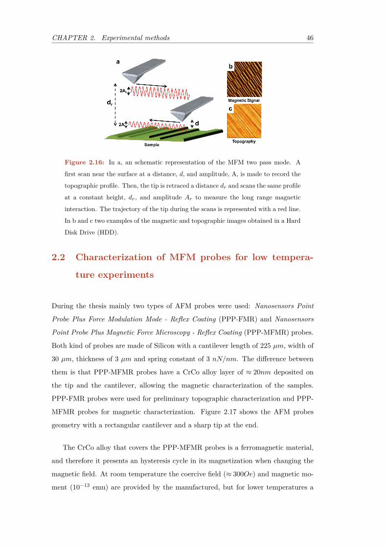
CHAPTER 2. Experimental methods 46
Figure 2.16: In a, an schematic representation of the MFM two pass mode. A
first scan near the surface at a distance, d, and amplitude, A, is made to record the
topographic profile. Then, the tip is retraced a distance dr and scans the same profile
at a constant height, dr, and amplitude Ar to measure the long range magnetic
interaction. The trajectory of the tip during the scans is represented with a red line.
In b and c two examples of the magnetic and topographic images obtained in a Hard
Disk Drive (HDD).
2.2 Characterization of MFM probes for low tempera-
ture experiments
During the thesis mainly two types of AFM probes were used: Nanosensors Point
Probe Plus Force Modulation Mode - Reflex Coating (PPP-FMR) and Nanosensors
Point Probe Plus Magnetic Force Microscopy - Reflex Coating (PPP-MFMR) probes.
Both kind of probes are made of Silicon with a cantilever length of 225 µm, width of
30 µm, thickness of 3 µm and spring constant of 3 nN/nm. The difference between
them is that PPP-MFMR probes have a CrCo alloy layer of ≈ 20nm deposited on
the tip and the cantilever, allowing the magnetic characterization of the samples.
PPP-FMR probes were used for preliminary topographic characterization and PPP-
MFMR probes for magnetic characterization. Figure 2.17 shows the AFM probes
geometry with a rectangular cantilever and a sharp tip at the end.
The CrCo alloy that covers the PPP-MFMR probes is a ferromagnetic material,
and therefore it presents an hysteresis cycle in its magnetization when changing the
magnetic field. At room temperature the coercive field (≈ 300Oe) and magnetic mo-
ment (10−13 emu) are provided by the manufactured, but for lower temperatures a
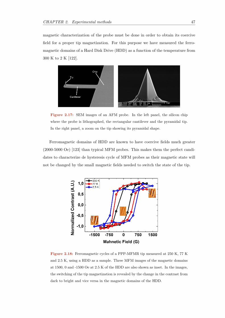
CHAPTER 2. Experimental methods 47
magnetic characterization of the probe must be done in order to obtain its coercive
field for a proper tip magnetization. For this purpose we have measured the ferro-
magnetic domains of a Hard Disk Drive (HDD) as a function of the temperature from
300 K to 2 K [122].
Figure 2.17: SEM images of an AFM probe. In the left panel, the silicon chip
where the probe is lithographed, the rectangular cantilever and the pyramidal tip.
In the right panel, a zoom on the tip showing its pyramidal shape.
Ferromagnetic domains of HDD are known to have coercive fields much greater
(2000-5000 Oe) [123] than typical MFM probes. This makes them the perfect candi-
dates to characterize de hysteresis cycle of MFM probes as their magnetic state will
not be changed by the small magnetic fields needed to switch the state of the tip.
Figure 2.18: Ferromagnetic cycles of a PPP-MFMR tip measured at 250 K, 77 K
and 2.5 K, using a HDD as a sample. Three MFM images of the magnetic domains
at 1500, 0 and -1500 Oe at 2.5 K of the HDD are also shown as inset. In the images,
the switching of the tip magnetization is revealed by the change in the contrast from
dark to bright and vice versa in the magnetic domains of the HDD.

CHAPTER 2. Experimental methods 48
The hysteresis cycle of a typical PPP-MFMR probe was recorded by measuring
the surface of a HDD at different fields and constant temperature for several tem-
peratures. We have calculated the magnetic moment of the tip (in arbitrary units)
as the difference in contrast between domains walls of the HDD in the MFM image
[124]. The hysteresis cycles for 250 K, 77 K and 2.5 K are represented in figure 2.18.
The coercive field of the tip changes from ≈ 300 Oe at RT to ≈ 1000 Oe at 2.5 K.
This characterization is extremely important for a proper interpretation of the
MFM images, as they are the result of the interaction of the tip magnetization and
the stray field of the sample [120].
2.2.0.1 MFM features
To illustrate the importance of the characterization of the MFM tips at low tempera-
tures, we will present the particular cases of MFM images of superconducting vortices
when a PPP-MFMR tip is magnetized below and above its coercive field.
If the tip is not magnetized above its coercive field, different domains with different
orientation can appear at the tip [125–127]. For example, let us discuss the images
shown in figure 2.19. In the images, superconducting vortices were measured in
β−Bi2Pd at 2 K with a tip magnetized with 500 Oe at 5 K, which is well below the
coercive field. As it was presented in the introduction of the thesis, superconducting
vortices are known to have circular shapes with radius determined by λ. In our
experiment, the superconducting vortices appear as star-like features instead of as
circles, pointing out the existence of a several magnetic domains on the tip, probably
at the sides of the pyramid (see figure 2.20 a). A simple explanation of the origin of
the star-like features will be discussed in the following:
The tip-vortex interaction can be approximately written as [128]:
δF
δz=mx
δ2Hx
δx2 +myδ2Hy
δy2 +mzδ2Hz
δz2 . (2.13)

CHAPTER 2. Experimental methods 49
Figure 2.19: Examples of star-like features at superconducting vortex positions
when a MFM tip is not magnetized up to its coercive field. The three MFM images
where taken at 2 K. Images a and b were taken at 100 Oe while c was taken at 200
Oe.
Where mi; i = x,y,z are the components of the magnetic dipolar moment of the
tip and Hi; i= x,y,z are the components of the field created by the vortex. The field
created by a vortex can be described as [28]:
B = φ02πλ2K0((r/λ)e
−2πzd (2.14)
where K0 is the modified Bessel functions of second order and r and z the radial
and vertical distances from the vortex core.
Most often, the X and Y components of the dipolar moment of the tip are neglected
[127]. This is justified, because the predominant magnetization of the tip is along the
z-axis. Here, however, we will take into account an in-plane magnetization. This
will lead to the observed star-shaped vortices. We consider a tip with non zero X
an Y components. By calculating spatial maps of the force gradient sensed by the
cantilever using equation 2.13, we find that indeed finite x and y components of the
magnetization provide star shaped vortices as is shown in Fig.2.20 c. The star-like
features obtained by our simple model, are very similar to the vortex shapes obtained
in the experiments. Real MFM images of star-like vortices are shown in figures 2.20
b and d together with the result of the simulations.
In order to compare the images obtained by a MFM tip magnetized below and
above its coercive field, we have measured the vortex lattice at the same area and the

CHAPTER 2. Experimental methods 50
Figure 2.20: In a, we schematically show a MFM tip with a non-zero in plane
component of the dipolar moment (grey arrow on the tip) and the vortex lattice
(coloured circles below). In b, we show star like vortices obtained at 2 K and 100 Oe
with a tip magnetized with 300 Oe at 5 K. In c and d we compare a simulation and an
MFM image of a single vortex measured with a tip with an in-plane magnetization
component. The same colour scale is used at the scheme, the simulation and the
MFM images.
same applied magnetic field with different tip magnetization conditions. In figure 2.21
two cases are shown, one with the tip magnetized at 500 Oe (below its coercive field)
and another with the tip magnetized at 1500 Oe (above its coercive field). When
the tip is magnetized below its coercive field, we observe in the images the features
provided by the interaction between the in-plane symmetric magnetic field of the
vortex and the tip’s anisotropic magnetic field distribution. Each vortex, imaged in
such conditions, thus mirrors the magnetic configuration of the tip.
2.3 Crystal growth
Binary phase diagrams contain the information of all known crystallographic struc-
tures for a pair of elements as a function of the composition and the temperature.
An example of a simple binary phase diagram for arbitrary elements, A and B, is
presented in figure 2.22.
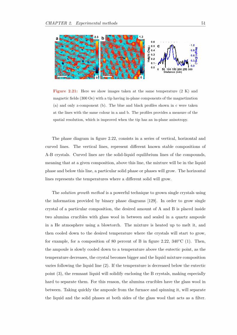
CHAPTER 2. Experimental methods 51
Figure 2.21: Here we show images taken at the same temperature (2 K) and
magnetic fields (300 Oe) with a tip having in-plane components of the magnetization
(a) and only z-component (b). The blue and black profiles shown in c were taken
at the lines with the same colour in a and b. The profiles provides a measure of the
spatial resolution, which is improved when the tip has an in-plane anisotropy.
The phase diagram in figure 2.22, consists in a series of vertical, horizontal and
curved lines. The vertical lines, represent different known stable compositions of
A-B crystals. Curved lines are the solid-liquid equilibrium lines of the compounds,
meaning that at a given composition, above this line, the mixture will be in the liquid
phase and below this line, a particular solid phase or phases will grow. The horizontal
lines represents the temperatures where a different solid will grow.
The solution growth method is a powerful technique to grown single crystals using
the information provided by binary phase diagrams [129]. In order to grow single
crystal of a particular composition, the desired amount of A and B is placed inside
two alumina crucibles with glass wool in between and sealed in a quartz ampoule
in a He atmosphere using a blowtorch. The mixture is heated up to melt it, and
then cooled down to the desired temperature where the crystals will start to grow,
for example, for a composition of 80 percent of B in figure 2.22, 340C (1). Then,
the ampoule is slowly cooled down to a temperature above the eutectic point, as the
temperature decreases, the crystal becomes bigger and the liquid mixture composition
varies following the liquid line (2). If the temperature is decreased below the eutectic
point (3), the remnant liquid will solidify enclosing the B crystals, making especially
hard to separate them. For this reason, the alumina crucibles have the glass wool in
between. Taking quickly the ampoule from the furnace and spinning it, will separate
the liquid and the solid phases at both sides of the glass wool that acts as a filter.
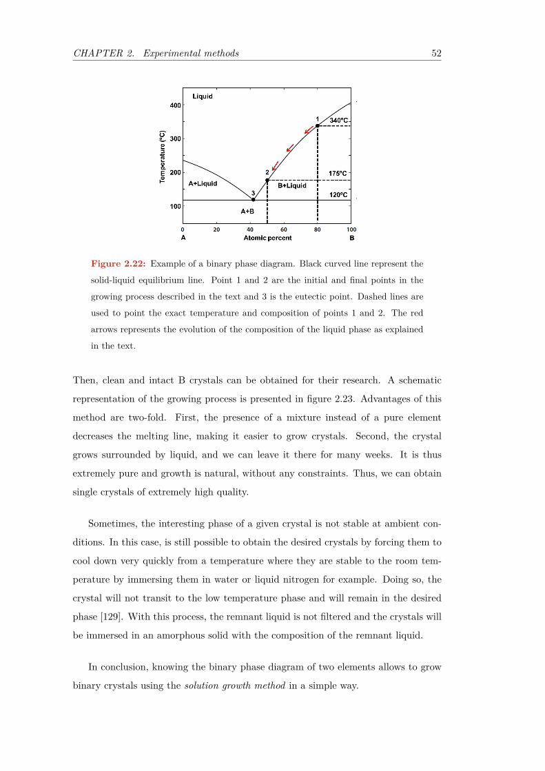
CHAPTER 2. Experimental methods 52
Figure 2.22: Example of a binary phase diagram. Black curved line represent the
solid-liquid equilibrium line. Point 1 and 2 are the initial and final points in the
growing process described in the text and 3 is the eutectic point. Dashed lines are
used to point the exact temperature and composition of points 1 and 2. The red
arrows represents the evolution of the composition of the liquid phase as explained
in the text.
Then, clean and intact B crystals can be obtained for their research. A schematic
representation of the growing process is presented in figure 2.23. Advantages of this
method are two-fold. First, the presence of a mixture instead of a pure element
decreases the melting line, making it easier to grow crystals. Second, the crystal
grows surrounded by liquid, and we can leave it there for many weeks. It is thus
extremely pure and growth is natural, without any constraints. Thus, we can obtain
single crystals of extremely high quality.
Sometimes, the interesting phase of a given crystal is not stable at ambient con-
ditions. In this case, is still possible to obtain the desired crystals by forcing them to
cool down very quickly from a temperature where they are stable to the room tem-
perature by immersing them in water or liquid nitrogen for example. Doing so, the
crystal will not transit to the low temperature phase and will remain in the desired
phase [129]. With this process, the remnant liquid is not filtered and the crystals will
be immersed in an amorphous solid with the composition of the remnant liquid.
In conclusion, knowing the binary phase diagram of two elements allows to grow
binary crystals using the solution growth method in a simple way.

CHAPTER 2. Experimental methods 53
Figure 2.23: Scheme of the solution growth method. Alumina crucibles are rep-
resented as beige cylinders and the quartz tubes with blue lines. In a, the desired
elements A and B (black and red circles) are placed inside the alumina crucibles.
Then in B, they are encapsulated between two alumina crucibles with quartz wool in
between (black line) and sealed in a quart tube in vacuum. In c, the quartz ampoule
is heated in a furnace to melt the elements inside and grow the crystals. Finally, in
d, the crystals are separated from the flux excess by spinning the quartz ampoule.
2.3.1 β−Bi2Pd single crystals growth
Figure 2.24: Phase diagram of Bismuth and Palladium system. The red line
represents the liquid-solid equilibrium line for β−Bi2Pd and the purple circle the
initial liquid concentration during the growth.
During the thesis, single crystals of β−Bi2Pd were grown using slight excess of
Bi [130], [131]. We grew our samples from high purity Bi (Alfa Aesar 99.99%) and Pd
(Alfa Aesar 99.95%). Bi and Pd were introduced in alumina crucibles and sealed in
quartz ampoules at 140 mbar of He gas using a blowtorch. Then, the ampoules were
heated from room temperature to 900C in 3 h, maintained 24 h at this temperature,
slowly cooled down to 490C in 96 h and finally cooled down to 395C in 200 h in
a furnace. This temperature is about 15C above the temperature for the formation

CHAPTER 2. Experimental methods 54
of the α−Bi2Pd phase [132] (figure 2.24). To avoid formation of the α phase, we
quenched the crystals down to ambient temperature by immersion in cold water. We
obtained large crystals of 5mm×5mm×3mm (inset in figure 2.25).
Figure 2.25: Powder diffraction pattern of β−Bi2Pd. Red symbols are the ex-
perimental points. The black line is the best fit to β−Bi2Pd diffraction pattern
[133]. Residuals are given by the blue line. The two series (upper and lower) of ver-
tical green strikes represent, respectively, the position in 2θ scale of the reflections
from the β−Bi2Pd (I4/mmm) and α−Bi2Pd (C12 =m1) phases. The inset show
a photograph of one β−Bi2Pd crystal. In b, the temperature dependence of the
resistivity. In c, the unit cell with the lattice parameters of β−Bi2Pd
To characterize them, we made x-ray diffraction on crystals milled down to powder
(Fig.2.25, using x rays with wavelength 1.54A). We find β−Bi2Pd (I4/mmm, see
Ref.[134]) with refined lattice parameters a= b= 3.36(8)A and c= 12.97(2)
A and no
trace of α−Bi2Pd. We made in total twelve growths, varying slightly the conditions
for the quench, growth temperature and initial composition, and obtained always
crystals with a resistivity vs temperature very similar to the one shown in Fig 2.25.
To ensure that the crystals composition is homogeneous on the whole crystal
and discard the presence of Bismuth or Pd clusters in it, we have performed Energy-
dispersive X-ray spectroscopy (EDX) measurements in a scanning electron microscope
(SEM) at the Servicio Interdepartamental de Investigacion (SIdI) of the Universidad
Autonoma de Madrid. We found that the 2:1 stoichiometry is constant in the whole
crystal and that there is not any presence of Bi or Pd precipitates on it. We have
measured the very same sample before and after exfoliating it using the Scotch tape
method, finding the same results in the outer and inner layers of the β −Bi2Pd
crystals. A SEM image of the crystal with the three different areas where EDX

CHAPTER 2. Experimental methods 55
experiments were performed is presented in figure 2.26.
Figure 2.26: In a, a SEM image of an β−Bi2Pd crystal. The pink rectangles
points the areas where different EDX spectres were measured. In b, the EDX spectra
measured in the area marked with a 2 in the SEM image. Each peak of the EDX
spectra is marked with the symbol of the corresponding element. The spectra at
different areas of the crystal show a perfect match with the Bi2Pd composition.
EDX experiments reveals and almost constant composition of ≈ 65at.% of Bi
and ≈ 35at.% of Pd on the whole sample, pointing out the very good quality of our
crystals. An example of the EDX spectra on the crystals is also presented in figure
2.26 b.
The superconducting vortex lattice in β−Bi2Pd at very low fields was measured
during the thesis and our result will be presented in chapter 4.
2.4 Summary and conclusions
In conclusion, we have successfully implemented an experimental set up that allows us
to perform AFM-MFM measurements between 1.8 K and 300 K, applying magnetic
fields in any direction of the space up to 5 T in the Z direction and 1.2 T in the
X and Y directions. With this set up, we have characterized the hysteresis cycle of
MFM commercial probes as a function of the temperature from 1.8 to 300 K. We have
also found that the MFM images of superconducting vortices show star-like features
at vortex positions when the MFM tip is magnetized below its coercive field. In
addition, during the thesis, single crystals of β−Bi2Pd were successfully grown via
the solution growth method and characterized.


CHAPTER 3
Exfoliation and characterization of layered
superconductors and graphene/superconductor
heterostructures
3.1 Introduction
The pioneering work published by Novoselov et al. [135] gave rise to the isolation
of single layers of graphene. They reported the repeated peeling of highly oriented
pyrolytic graphite (HOPG) on a photoresist layer and the final release of the resulting
thin flakes in acetone. This method was later improved with the dry exfoliation
of several layered materials by simply pressing the surface of crystalline samples
against different surfaces [136]. This basic methodology gave access to large surface
area flakes of atomically-thin graphene and also to flakes of certain transition metals
dichalcogenides (TMDCs) like the superconducting NbSe2 or MoS2 among others [3–
6]. The technique was implemented in a variety of different ways under the generic
name of micromechanical cleavage also known in informal terms as the Scotch tape
method.
During the last decade a great variety of different mechanical cleavage methods
were developed for the clean deposition of 2D materials on different surfaces. Among
them, we can highlight micromechanical exfoliation techniques based on the use of
57
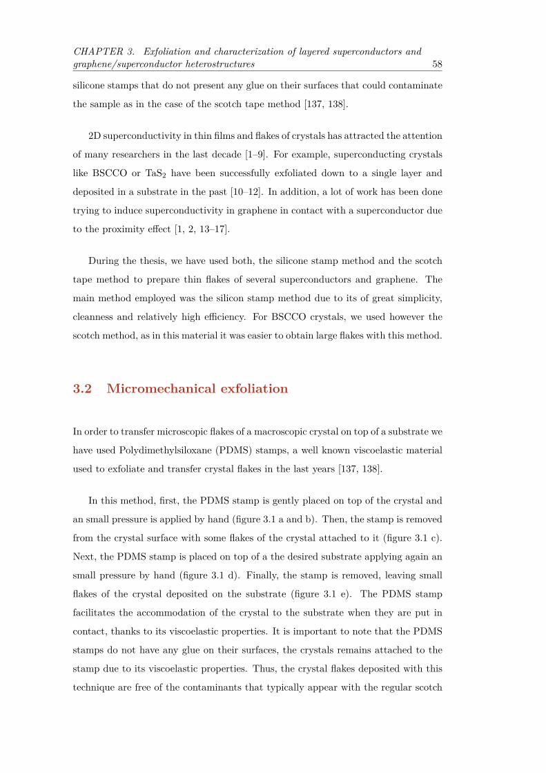
CHAPTER 3. Exfoliation and characterization of layered superconductors andgraphene/superconductor heterostructures 58
silicone stamps that do not present any glue on their surfaces that could contaminate
the sample as in the case of the scotch tape method [137, 138].
2D superconductivity in thin films and flakes of crystals has attracted the attention
of many researchers in the last decade [1–9]. For example, superconducting crystals
like BSCCO or TaS2 have been successfully exfoliated down to a single layer and
deposited in a substrate in the past [10–12]. In addition, a lot of work has been done
trying to induce superconductivity in graphene in contact with a superconductor due
to the proximity effect [1, 2, 13–17].
During the thesis, we have used both, the silicone stamp method and the scotch
tape method to prepare thin flakes of several superconductors and graphene. The
main method employed was the silicon stamp method due to its of great simplicity,
cleanness and relatively high efficiency. For BSCCO crystals, we used however the
scotch method, as in this material it was easier to obtain large flakes with this method.
3.2 Micromechanical exfoliation
In order to transfer microscopic flakes of a macroscopic crystal on top of a substrate we
have used Polydimethylsiloxane (PDMS) stamps, a well known viscoelastic material
used to exfoliate and transfer crystal flakes in the last years [137, 138].
In this method, first, the PDMS stamp is gently placed on top of the crystal and
an small pressure is applied by hand (figure 3.1 a and b). Then, the stamp is removed
from the crystal surface with some flakes of the crystal attached to it (figure 3.1 c).
Next, the PDMS stamp is placed on top of a the desired substrate applying again an
small pressure by hand (figure 3.1 d). Finally, the stamp is removed, leaving small
flakes of the crystal deposited on the substrate (figure 3.1 e). The PDMS stamp
facilitates the accommodation of the crystal to the substrate when they are put in
contact, thanks to its viscoelastic properties. It is important to note that the PDMS
stamps do not have any glue on their surfaces, the crystals remains attached to the
stamp due to its viscoelastic properties. Thus, the crystal flakes deposited with this
technique are free of the contaminants that typically appear with the regular scotch

CHAPTER 3. Exfoliation and characterization of layered superconductors andgraphene/superconductor heterostructures 59
Figure 3.1: In a, b and c, we show the exfoliation process using a PDMS stamp.
First, the stamp is gently pushed against the clean crystal surface and then they are
separated. Some crystals flakes are attached to the stamp after separating it from
the crystal. In d and e, we schematically show the deposition of the crystal flakes
on top of a substrate. The PDMS stamp is pushed against the substrate and few
flakes are deposited on top of it. In f and g, we show two optical images of arbitrary
β-Bi2Pd flakes deposited on a SiO2 substrate. In h, we show a real picture of the
PDMS stamp with some crystal flakes attached on top.
tape method [139]. A schematic representation of the exfoliation-transfer method is
represented in figure 3.1 together with some pictures of the deposited flakes and the
stamp.
After depositing the crystal flakes on top of a substrate, they are localized using an
optical microscope using a combination of x10, x50 and x100 zoom lenses (figure 3.2
a and b). Then, the sample is moved to our room temperature AFM (RT-AFM) and
the same area is localized with another optical microscope integrated with the RT-
AFM (figure 3.2 c). Finally, the flakes are measured with the RT-AFM to determine
their height.

CHAPTER 3. Exfoliation and characterization of layered superconductors andgraphene/superconductor heterostructures 60
Figure 3.2: In a and b, we show two pictures of two β-Bi2Pd flakes deposited on
top of a SiO2 substrate with zooms x10 and x100 respectively. In both images the
position of the flakes are highlighted with yellow and red circles or ellipses. In c, the
same area imaged with an optical microscope integrated with our RT-AFM showing
the AFM cantilever above the area where the crystal flakes are deposited.
3.2.1 BSCCO on SiO2
We have exfoliated BSCCO crystals down to a few layers and deposited them on a Si
substrate with a SiO2 layer of 300 nm on top, following the same procedure described
in the previous section. We have successfully localized and measured a 25 nm thick
flake at low temperatures under different magnetic applied fields in our LT-MFM.
3.2.1.1 Moderate magnetic fields
First, we have localized the flake at 10 K and measured its topography and magnetic
profile under an applied magnetic field of 100 Oe in the out of plane direction, as is
shown in figure 3.3. We have found that the magnetic profile was homogeneous in
the whole field of view. This homogeneity can be understood as an increment in the
size of the superconducting vortices in very thin samples proposed by Pearl in 1964
[140].
The main problem of magnetic images in thin superconducting material is the
evolution of the penetration depth as the thickness of the superconductor decreases.
The thin-film problem differs from the behavior of currents and vortices in bulk
superconductors by the dominating role of the magnetic stray field outside the film.
The interaction between vortices occurs mainly by this stray field, while in bulk
superconductors the vortex currents and the vortex interaction are screened and thus
decrease exponentially over the length λ [140–142].

CHAPTER 3. Exfoliation and characterization of layered superconductors andgraphene/superconductor heterostructures 61
Figure 3.3: In a, we show the topographic image measured at 10 K of a BSCCO
flake deposited on a SiO2 substrate. In b, we show the corresponding magnetic image
measured under an applied magnetic field of 100 Oe at 10 K. From the images is
clear that the magnetic profile is homogeneous at the BSCCO flake surface.
If we consider one vortex in the center of a large circular film with infinite radius
and in the limit of zero λ. The point vortex behaves like a magnetic dipole, composed
of two magnetic monopoles: one above and another below the film. The magnetic
field lines of this point-vortex are straight radial lines, all passing through this point.
The magnitude of this magnetic stray field is φ0/2πr2 above and −φ0/2πr2 below the
film. The magnetic field parallel to the film suffers a discontinuity and a sheet current
circulates around the vortex with J = φ0/µ0πr2. This result differs form the strong
decay of screening currents of bulk superconductors, J = φ02πµ0λ3K1(r/λ) [28], where
K1 is the first order modified Bessel function. In his original paper, Pearl found and
effective penetration depth for superconductors when d < λ (d the thickness of the
superconductor). This effective penetration depth is Λ = 2λ2/d. Where Λ is known
as the Pearl penetration depth.
The expected penetration depth for a BSCCO crystal is ≈ 200 nm [143–145], in
good agreement with our LT-MFM measurements in chapter 6. Therefore, for a flake
25 nm thick, a Pearl penetration depth of≈ 5 µm is expected. From equation 1.14, the
intervortex distance at a magnetic field of 100 Oe is expected to be ≈ 500 nm. Thus,
the magnetic profile on the superconductor is expected to become homogeneous, in
good agreement with our measurements.
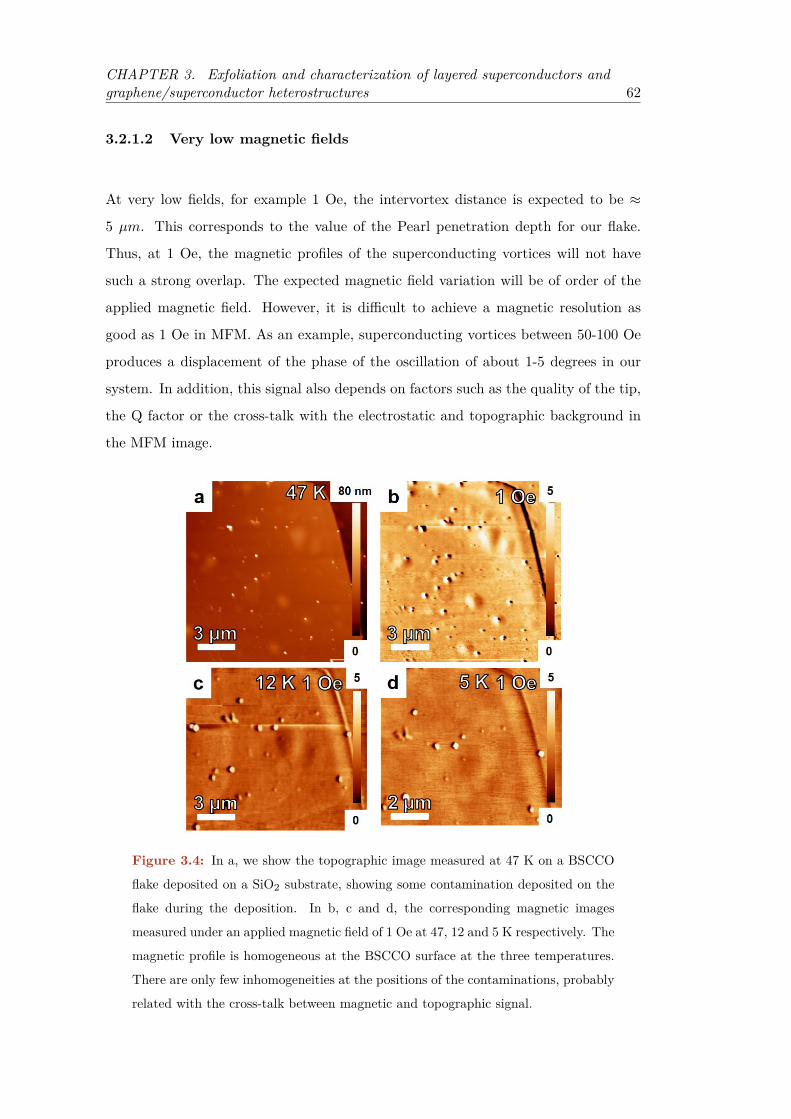
CHAPTER 3. Exfoliation and characterization of layered superconductors andgraphene/superconductor heterostructures 62
3.2.1.2 Very low magnetic fields
At very low fields, for example 1 Oe, the intervortex distance is expected to be ≈
5 µm. This corresponds to the value of the Pearl penetration depth for our flake.
Thus, at 1 Oe, the magnetic profiles of the superconducting vortices will not have
such a strong overlap. The expected magnetic field variation will be of order of the
applied magnetic field. However, it is difficult to achieve a magnetic resolution as
good as 1 Oe in MFM. As an example, superconducting vortices between 50-100 Oe
produces a displacement of the phase of the oscillation of about 1-5 degrees in our
system. In addition, this signal also depends on factors such as the quality of the tip,
the Q factor or the cross-talk with the electrostatic and topographic background in
the MFM image.
Figure 3.4: In a, we show the topographic image measured at 47 K on a BSCCO
flake deposited on a SiO2 substrate, showing some contamination deposited on the
flake during the deposition. In b, c and d, the corresponding magnetic images
measured under an applied magnetic field of 1 Oe at 47, 12 and 5 K respectively. The
magnetic profile is homogeneous at the BSCCO surface at the three temperatures.
There are only few inhomogeneities at the positions of the contaminations, probably
related with the cross-talk between magnetic and topographic signal.

CHAPTER 3. Exfoliation and characterization of layered superconductors andgraphene/superconductor heterostructures 63
We have imaged again the magnetic profile of the same flake at very low applied
magnetic fields (1 Oe) and different temperatures. Our results are summarized in
figure 3.4 and 3.5. In figure 3.4, we show three magnetic images with a magnetic
field of 1 Oe at 47, 12 and 5 K together with the corresponding topographic image.
As it is clear from the images, the magnetic profiles are homogeneous in the whole
field of view at the three temperatures, presenting only small variations probably
of non-magnetic origin and related with the contamination deposited on top of the
flake during the exfoliation. The homogeneity of the magnetic profiles indicates that
besides all our efforts, our magnetic resolution is not good enough to allow single
vortex resolution at 1 Oe. From the images is clear that the cross-talk with the
topographic profile of the sample is stronger that the magnetic signal.
We have also measured a region where the edge of the BSCCO flake and the SiO2
substrate are clearly visible to determine if there is any measurable screening of the
magnetic field in the superconducting flake with respect to the substrate. Our results
are presented in figure 3.5. The magnetic image in figure 3.5 shows that the magnetic
profile is homogeneous in the whole field of view. There is not measurable difference
between the region occupied by the superconductor with respect to the substrate.
There is only some contrast in the magnetic image at the positions of the edge of the
BSCCO flake and of a longitudinal topographic feature in the right part of the image,
due to the cross-talk with the topographic profile at this locations.
Unfortunately, the screening of the magnetic field in the superconducting flake
with respect to the substrate is below our experimental resolution at this thickness.
Thus, we were not able to measure the existence of Pearl vortices or another supercon-
ducting effect related with the thickness in our experiments on BSCCO. Nevertheless,
we were able to deposit thin flakes of this material and localize them at low temper-
atures opening the possibility for further experiment in BSCCO flakes of different
thicknesses in the future.
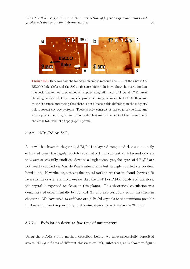
CHAPTER 3. Exfoliation and characterization of layered superconductors andgraphene/superconductor heterostructures 64
Figure 3.5: In a, we show the topographic image measured at 17 K of the edge of the
BSCCO flake (left) and the SiO2 substrate (right). In b, we show the corresponding
magnetic image measured under an applied magnetic fields of 1 Oe at 17 K. From
the image is clear that the magnetic profile is homogeneous at the BSCCO flake and
at the substrate, indicating that there is not a measurable difference in the magnetic
field between the two systems. There is only contrast at the edge of the flake and
at the position of longitudinal topographic feature on the right of the image due to
the cross-talk with the topographic profile.
3.2.2 β-Bi2Pd on SiO2
As it will be shown in chapter 4, β-Bi2Pd is a layered compound that can be easily
exfoliated using the regular scotch tape method. In contrast with layered crystals
that were successfully exfoliated down to a single monolayer, the layers of β-Bi2Pd are
not weakly coupled via Van de Waals interactions but strongly coupled via covalent
bonds [146]. Nevertheless, a recent theoretical work shows that the bonds between Bi
layers in the crystal are much weaker that the Bi-Pd or Pd-Pd bonds and therefore,
the crystal is expected to cleave in this planes. This theoretical calculation was
demonstrated experimentally by [23] and [24] and also corroborated in this thesis in
chapter 4. We have tried to exfoliate our β-Bi2Pd crystals to the minimum possible
thickness to open the possibility of studying superconductivity in the 2D limit.
3.2.2.1 Exfoliation down to few tens of nanometers
Using the PDMS stamp method described before, we have successfully deposited
several β-Bi2Pd flakes of different thickness on SiO2 substrates, as is shown in figure

CHAPTER 3. Exfoliation and characterization of layered superconductors andgraphene/superconductor heterostructures 65
3.6.
Figure 3.6: In the left panel, two AFM images of two β-Bi2Pd flakes deposited on
top of a SiO2 substrate. In the right panel, the corresponding topographic profiles
marked as green lines on the images in the left. The images show the possibility of
depositing flake of β-Bi2Pd of different thicknesses.
In the image, two examples of β-Bi2Pd flakes are presented, one thick flake of
several hundreds of nanometers and a thin flake of just some tens of nanometers.
The thin flake reveals that it is possible to exfoliate a β-Bi2Pd single crystal down
to very small thicknesses. Unfortunately, the density of thin flakes of β-Bi2Pd that
we achieved with the stamp method was not enough to allow us to localize one of
these flakes at low temperatures. The thermal drift of our LT-MFM prevents us to
locate a β-Bi2Pd flakes at low temperature despite all our efforts. More work is need
in this direction to investigate the superconducting behavior of β-Bi2Pd thin flakes.
In particular, improving the deposition technique to increase the ratio of success and
reduce the thermal drift of the microscope are of particular interest in this or any
other system in form of flakes of small lateral sizes.
3.2.3 Graphene on β-Bi2Pd
We have successfully exfoliated several graphene and few-layers-graphene (FLG) flakes
and deposited them on top of a single crystal of the superconductor β-Bi2Pd. The

CHAPTER 3. Exfoliation and characterization of layered superconductors andgraphene/superconductor heterostructures 66
flakes were characterized with our RT-AFM after localizing them with an optical
microscope. An example is shown in figure 3.7, where three pictures at different
magnifications are presented together with a topographic AFM image. The AFM
topographic measurements show a combination of several FLG flakes at the edge of
the big graphite flake.
Figure 3.7: In a b and c, three optical images with magnifications x10, x50 and
x100, used to localize the graphene flakes deposited on to of the β-Bi2Pd crystal. In
d, the corresponding topographic image of the area highlighted with a black square
in c. It shows flakes with different thicknesses with a graphene flake marked with a
black arrow
3.2.3.1 Friction measurements
It is know that graphene has lubricant properties [147]. TThis facilitates the location
of the flakes via friction images, as the contrast in friction images between graphene,
FLG and the substrates is often large [148]. For this reason, we have performed a
combination of topographic and friction measurements at the same flake to localize
the different graphene or FLG flakes.
The physical basics of the friction measurements in AFM are as follows. When

CHAPTER 3. Exfoliation and characterization of layered superconductors andgraphene/superconductor heterostructures 67
scanning in the contact mode at a constant force, besides the cantilever’s deflection
in the normal direction, an additional torsion of the cantilever takes place. When
moving over a flat surface with zones of different friction factors, the angle of torsion
will be changing in every new zone. This allows measuring of the local friction force
(for a detailed study of friction measurements in AFM see reference [120]).
In figure 3.8 b, there are several FLG flakes on the right of the image that are
not easily visible in the topographic image. They appear as a clear dark contrast in
the friction image. In our case, we have not found mayor differences between friction
images on graphene and FLG on top of the β-Bi2Pd crystal, probably due to surface
contamination during the exfoliation-transfer method. Friction images do not allow
us to distinguish between graphene or FLG flakes on top of β-Bi2Pd but is still the
best technique to quickly localize FLG flakes on top of β-Bi2Pd that are not visible
in the topographic image.
3.2.3.2 Kelvin Probe Microscopy (KPM) measurements
We have used a different approach to establish a experimental procedure that un-
ambiguously distinguishes between graphene and FLG flakes deposited on β-Bi2Pd.
We have performed Kelvin Probe Microscopy (KPM) measurements on the same
flake to characterize the surface potential difference between the β-Bi2Pd substrate,
graphene and FLG flakes. KPM is a tool that enables nanometer-scale imaging of the
surface potential of a broad range of materials. KPM measures the Surface Potential
Difference (SPD) between a conducting tip and the sample.
VSPD = φtip−φsample−e
(3.1)
Where φtip and φsample are the work functions of the tip and the sample (for a
more detailed study of the KPM see reference [120]).
In figure 3.8 c and d, KPM maps at the same areas that the topographic and
friction images are shown. In this case, is clear that the difference in surface potential
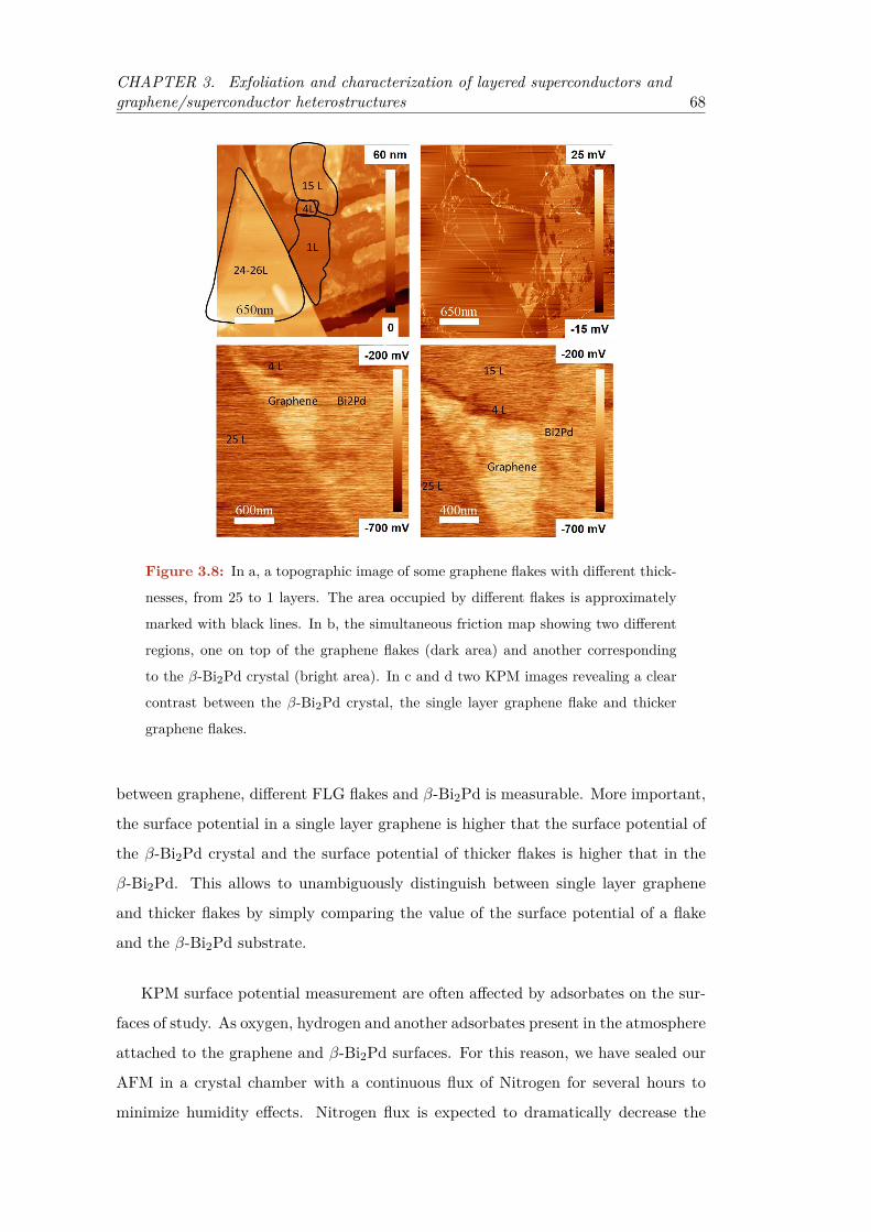
CHAPTER 3. Exfoliation and characterization of layered superconductors andgraphene/superconductor heterostructures 68
Figure 3.8: In a, a topographic image of some graphene flakes with different thick-
nesses, from 25 to 1 layers. The area occupied by different flakes is approximately
marked with black lines. In b, the simultaneous friction map showing two different
regions, one on top of the graphene flakes (dark area) and another corresponding
to the β-Bi2Pd crystal (bright area). In c and d two KPM images revealing a clear
contrast between the β-Bi2Pd crystal, the single layer graphene flake and thicker
graphene flakes.
between graphene, different FLG flakes and β-Bi2Pd is measurable. More important,
the surface potential in a single layer graphene is higher that the surface potential of
the β-Bi2Pd crystal and the surface potential of thicker flakes is higher that in the
β-Bi2Pd. This allows to unambiguously distinguish between single layer graphene
and thicker flakes by simply comparing the value of the surface potential of a flake
and the β-Bi2Pd substrate.
KPM surface potential measurement are often affected by adsorbates on the sur-
faces of study. As oxygen, hydrogen and another adsorbates present in the atmosphere
attached to the graphene and β-Bi2Pd surfaces. For this reason, we have sealed our
AFM in a crystal chamber with a continuous flux of Nitrogen for several hours to
minimize humidity effects. Nitrogen flux is expected to dramatically decrease the

CHAPTER 3. Exfoliation and characterization of layered superconductors andgraphene/superconductor heterostructures 69
Figure 3.9: In a, our RT-AFM with the crystal chamber used to control the ambient
humidity with the N2 flux. In b, a KPM image measured during the experiment
as an example. In c, the evolution of the surface potential for the substrate (β-
Bi2Pd), graphene and FLG after decrease the humidity of the sample chamber by
applying a constant flux of N2. The moment when the N2 flux was switch on is
marked in gray. In d, the evolution of the surface potential of the same system as a
function of the number of layers of graphene for four different times after decreasing
the humidity. Both plots show that the surface potential difference between the
β-Bi2Pd, the graphene and the FLG remains almost constant with the time.
humidity inside the crystal chamber and partially remove the adsorbates from the
sample. We have maintained the Nitrogen flux for 50 hours, performing several KPM
measurement during the process. We have found that the Surface potential of all
FLG, graphene and β-Bi2Pd decreases with the time and approaches an stable value
after turning on the N2 flux. After reaching a stable value, the difference between the
surface potential of the different flakes and the β-Bi2Pd substrate, is almost the same
than before, showing that this technique allows to localize graphene flakes even at
ambient conditions with contaminants deposited on the surface. The results of this
experiment are summarized in figure 3.9.

CHAPTER 3. Exfoliation and characterization of layered superconductors andgraphene/superconductor heterostructures 70
Our results shows that KPM a suitable experimental microscopic technique to
individual localize graphene flakes on top of the superconductor β-Bi2Pd. By contrast
friction maps have probed to be a valuable tool to localize graphene and FLG flakes on
top of β-Bi2Pd but no dot allow to unambiguously determine the number of graphene
layers.
3.3 Conclusions
In conclusion, we have successfully exfoliated several superconducting crystals and
graphene and deposit them in different substrates using a combination of PDMS sili-
con stamps and the regular scotch tape method. We have investigated three different
system with this method, BSCCO on SiO2, β-Bi2Pd on SiO2 and graphene and FLG
on β-Bi2Pd.
In the case of BSCCO flakes deposited in SiO2, we were able to measure one thick
flake at low temperatures and characterize its magnetic profile in the superconducting
state at different magnetic fields and temperatures. We have found that the screening
of the magnetic field in this flakes is bellow our experimental resolution at moderate
(100 Oe) and very low fields (1 Oe).
For β-Bi2Pd flakes deposited on SiO2, we were able to exfoliate and deposit flakes
of this system for the very first time, down to some tens of nanometers. These results
open the possibility to study the superconducting behavior in the 2D limit in this
system in the future.
We have also transferred graphene and FLG flakes on top of a β-Bi2Pd single
crystal and developed a experimental procedure to unambiguously localize graphene
and FLG flakes on top of β-Bi2Pd using a combination of friction and KPM mea-
surements with an AFM. We have also probed that this method allow to localize the
flakes at ambient and at low humidity conditions.

CHAPTER 4
Vortex lattice at very low fields in the low κ
superconductor β−Bi2Pd and
β−Bi2Pd/graphene heterostructures
4.1 Introduction
Historically, magnetic microscopy techniques have been of huge importance in the
study of superconducting materials. The first visualization of the vortex lattice was
achieved by Essman and Trauble [149] in Pb by Bitter magnetic decoration in 1967
(figure 4.1 a). The Bitter decoration technique consists in depositing small magnetic
particles on the surface of the superconductor. Under a magnetic field, the magnetic
particles arrange at the positions of the flux lines, indicating the location of individual
vortices. Bitter decoration was also the first technique used to visualize the vortex
lattice in high TC superconductors in 1987 by Gammel et al. [150] in YBCO (figure 4.1
b). The MFM was used for first time to measure the vortex lattice in a superconductor
in YBCO by Moser et al. [151] in 1995 (figure 4.1 c).
A few pioneering works of magnetic bitter decoration have studied the intermedi-
ate state in Type I and the intermediate mixed state (IMS) in Type II superconductors,
proving the coexistence between domains of normal and Meissner state in type I and
between Meissner and mixed state in type II superconductors [37, 39, 40, 152, 153].
71
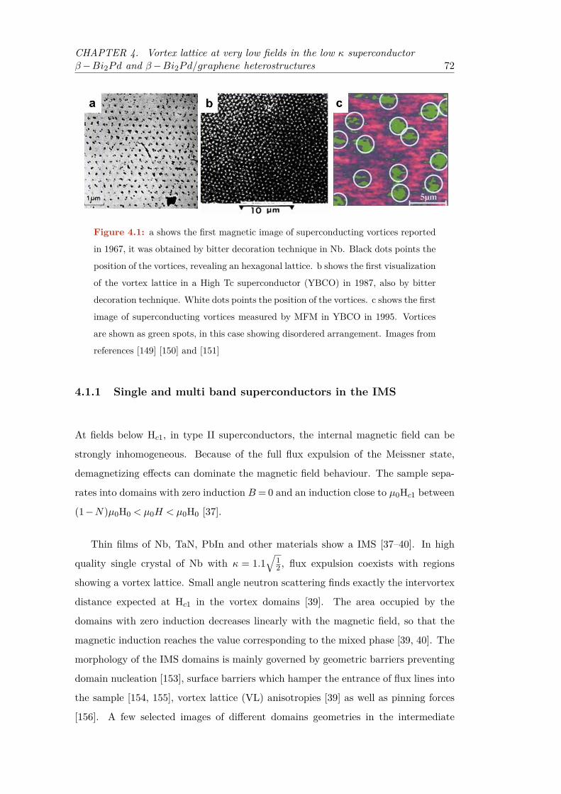
CHAPTER 4. Vortex lattice at very low fields in the low κ superconductorβ−Bi2Pd and β−Bi2Pd/graphene heterostructures 72
Figure 4.1: a shows the first magnetic image of superconducting vortices reported
in 1967, it was obtained by bitter decoration technique in Nb. Black dots points the
position of the vortices, revealing an hexagonal lattice. b shows the first visualization
of the vortex lattice in a High Tc superconductor (YBCO) in 1987, also by bitter
decoration technique. White dots points the position of the vortices. c shows the first
image of superconducting vortices measured by MFM in YBCO in 1995. Vortices
are shown as green spots, in this case showing disordered arrangement. Images from
references [149] [150] and [151]
4.1.1 Single and multi band superconductors in the IMS
At fields below Hc1, in type II superconductors, the internal magnetic field can be
strongly inhomogeneous. Because of the full flux expulsion of the Meissner state,
demagnetizing effects can dominate the magnetic field behaviour. The sample sepa-
rates into domains with zero induction B = 0 and an induction close to µ0Hc1 between
(1−N)µ0H0 < µ0H < µ0H0 [37].
Thin films of Nb, TaN, PbIn and other materials show a IMS [37–40]. In high
quality single crystal of Nb with κ = 1.1√
12 , flux expulsion coexists with regions
showing a vortex lattice. Small angle neutron scattering finds exactly the intervortex
distance expected at Hc1 in the vortex domains [39]. The area occupied by the
domains with zero induction decreases linearly with the magnetic field, so that the
magnetic induction reaches the value corresponding to the mixed phase [39, 40]. The
morphology of the IMS domains is mainly governed by geometric barriers preventing
domain nucleation [153], surface barriers which hamper the entrance of flux lines into
the sample [154, 155], vortex lattice (VL) anisotropies [39] as well as pinning forces
[156]. A few selected images of different domains geometries in the intermediate
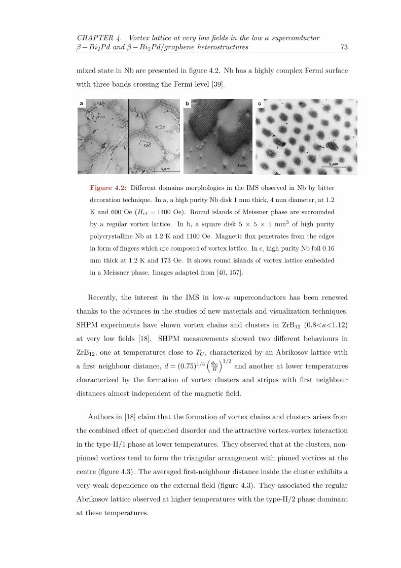
CHAPTER 4. Vortex lattice at very low fields in the low κ superconductorβ−Bi2Pd and β−Bi2Pd/graphene heterostructures 73
mixed state in Nb are presented in figure 4.2. Nb has a highly complex Fermi surface
with three bands crossing the Fermi level [39].
Figure 4.2: Different domains morphologies in the IMS observed in Nb by bitter
decoration technique. In a, a high purity Nb disk 1 mm thick, 4 mm diameter, at 1.2
K and 600 Oe (Hc1 = 1400 Oe). Round islands of Meissner phase are surrounded
by a regular vortex lattice. In b, a square disk 5 × 5 × 1 mm3 of high purity
polycrystalline Nb at 1.2 K and 1100 Oe. Magnetic flux penetrates from the edges
in form of fingers which are composed of vortex lattice. In c, high-purity Nb foil 0.16
mm thick at 1.2 K and 173 Oe. It shows round islands of vortex lattice embedded
in a Meissner phase. Images adapted from [40, 157].
Recently, the interest in the IMS in low-κ superconductors has been renewed
thanks to the advances in the studies of new materials and visualization techniques.
SHPM experiments have shown vortex chains and clusters in ZrB12 (0.8<κ<1.12)
at very low fields [18]. SHPM measurements showed two different behaviours in
ZrB12, one at temperatures close to TC , characterized by an Abrikosov lattice with
a first neighbour distance, d = (0.75)1/4(
Φ0B
)1/2and another at lower temperatures
characterized by the formation of vortex clusters and stripes with first neighbour
distances almost independent of the magnetic field.
Authors in [18] claim that the formation of vortex chains and clusters arises from
the combined effect of quenched disorder and the attractive vortex-vortex interaction
in the type-II/1 phase at lower temperatures. They observed that at the clusters, non-
pinned vortices tend to form the triangular arrangement with pinned vortices at the
centre (figure 4.3). The averaged first-neighbour distance inside the cluster exhibits a
very weak dependence on the external field (figure 4.3). They associated the regular
Abrikosov lattice observed at higher temperatures with the type-II/2 phase dominant
at these temperatures.

CHAPTER 4. Vortex lattice at very low fields in the low κ superconductorβ−Bi2Pd and β−Bi2Pd/graphene heterostructures 74
Figure 4.3: Vortex cluster formation in ZrB12. In the left panel, SHPM images
observed at 4.2 K after FC with progressively increasing magnetic fields, showing
the formation of a vortex cluster. The symbols indicate the location of the vortices.
Squares points the position of vortices pinned on defects and circles of vortices not
pinned on defects. In the right panel, averaged nearest-neighbour distance as a
function of the applied magnetic field for the vortex cluster (green circles). The
nearest-neighbour distance for the VL at 5.85 K is shown by the squares, which
follows the triangular arrangement of the Abrikosov VL (dashed line). Adapted
from [18]
On the other hand, 2H-NbSe2 and MgB2 show two superconducting gaps. In
MgB2, interband interactions are weak, whereas they appear to be stronger in NbSe2
[158–160]. Both are extreme type II superconductors, with κ 1√2 [161]. Several
experiments to characterize the vortex lattice below HC1 have been done in these two
materials using different magnetic microscopic techniques [19–21].
Bitter decoration studies at very low fields showed a remarkable different be-
haviour between 2H-NbSe2 and MgB2 [19]. Decoration measurements in 2H-NbSe2
show a distorted hexagonal lattice (figure 4.4 a) while in MgB2, they show vortex
accumulation in clusters at H=1 Oe and in stripes at H=5 Oe (figure 4.4 b and
c). Clusters and stripes are separated by vortex free areas, whose size is of a few
intervortex distances. Further Scanning SQUID measurements in MgB2 showed ac-
cumulation of vortices in clusters with an intervortex distance almost independent
of the magnetic field [21]. Moreover, SHPM measurements at very low fields showed
a hexagonal lattice for NbSe2 with the intervortex distance expected for the applied
magnetic field (figure 4.5 a and b) and vortex accumulation in clusters and stripes in
MgB2 [20] (figure 4.5 c and d).

CHAPTER 4. Vortex lattice at very low fields in the low κ superconductorβ−Bi2Pd and β−Bi2Pd/graphene heterostructures 75
Figure 4.4: Bitter decoration images of the vortex structure at very low fields
in 2H-NbSe2 and MgB2. Vortex positions are shown as white dots on the blue
background. In a, vortices in NbSe2 in a distorted triangular lattice at T = 4.2 K
and H = 1 Oe. In b, vortices in MgB2 are accumulated in clusters at T = 4.2 K and
H = 1 Oe. In c, vortices in MgB2 are accumulated in stripes at T = 4.2 K and H =
5 Oe. Images adapted form [19].
Figure 4.5: Scanning Hall Microscopy images of the vortex structure at very low
fields in 2H-NbSe2 and MgB2. In a and b, SHPM images of a distorted triangular
vortex lattice in NbSe2 at 4.2 K and 2 Oe. In c and d, SHPM images of stripes and
clusters of vortices in MgB2 at 4.2K and 2 Oe.
The hexagonal lattice found in 2H-NbSe2 was ascribed to vortices nucleated in
the mixed state at temperatures where H0 = 0[20]. Vortices are formed at high
temperatures, when Hc1(T ) is negligible and remain trapped when cooling. Vortices
then, form hexagonal lattice with a first neighbour distance, d = (0.75)1/4(
Φ0B
)1/2
and are retained at low temperatures by surface barriers [162]. No vortex free areas
have been reported in 2H-NbSe2.
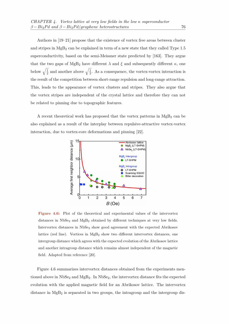
CHAPTER 4. Vortex lattice at very low fields in the low κ superconductorβ−Bi2Pd and β−Bi2Pd/graphene heterostructures 76
Authors in [19–21] propose that the existence of vortex free areas between cluster
and stripes in MgB2 can be explained in term of a new state that they called Type 1.5
superconductivity, based on the semi-Meissner state predicted by [163]. They argue
that the two gaps of MgB2 have different λ and ξ and subsequently different κ, one
below√
12 and another above
√12 . As a consequence, the vortex-vortex interaction is
the result of the competition between short-range repulsion and long-range attraction.
This, leads to the appearance of vortex clusters and stripes. They also argue that
the vortex stripes are independent of the crystal lattice and therefore they can not
be related to pinning due to topographic features.
A recent theoretical work has proposed that the vortex patterns in MgB2 can be
also explained as a result of the interplay between repulsive-attractive vortex-vortex
interaction, due to vortex-core deformations and pinning [22].
Figure 4.6: Plot of the theoretical and experimental values of the intervortex
distances in NbSe2 and MgB2 obtained by different techniques at very low fields.
Intervortex distances in NbSe2 show good agreement with the expected Abrikosov
lattice (red line). Vortices in MgB2 show two different intervortex distances, one
intergroup distance which agrees with the expected evolution of the Abrikosov lattice
and another intragroup distance which remains almost independent of the magnetic
field. Adapted from reference [20].
Figure 4.6 summarizes intervortex distances obtained from the experiments men-
tioned above in NbSe2 and MgB2. In NbSe2, the intervortex distance fits the expected
evolution with the applied magnetic field for an Abrikosov lattice. The intervortex
distance in MgB2 is separated in two groups, the intragroup and the intergroup dis-
CHAPTER 4. Vortex lattice at very low fields in the low κ superconductorβ−Bi2Pd and β−Bi2Pd/graphene heterostructures 77
tances. The intragroup distance remains almost constant when changing the magnetic
field while the intergroup distance follows the expected behavior of the Abrikosov lat-
tice [20].
Comparatively, β−Bi2Pd has a small, yet sizable, value of κ≈ 6. It has very weak
pinning and is a single gap isotropic superconductor [23–25].
4.1.2 Previous works on β−Bi2Pd crystals
In 2012 Imai et al. [164] grew β−Bi2Pd single crystals and suggested the possibility
of a multigap behaviour. Their macroscopic measurements appeared to be consistent
with multigap superconductivity. Their specific heat measurements showed a peculiar
behaviour below TC when changing the temperature, similar to the observed in the
two gap superconductors MgB2 and Lu2Fe3Si5 (the magnitude of the discontinuity
at TC , a fast increase at low-temperature and a small shoulder in between) [165–167]
(figure 4.7 b). Moreover, their HC2 measurements as a function of temperature were
also consistent with the two gap scenario as they showed positive curvature near the
critical temperature similar to other multi-gap superconductors [168–171] (figure 4.7
c).
The results mentioned in the last paragraph can be explained as follows. The
curvature of the upper critical field is due to the presence of a surface sheet that
influences the resistive transition [25] and the curvature of the specific heat probably
due to the difficulties associated to the extraction of the superconducting specific heat
from the phonon component, as the measurements in [25] suggest. Thus, beta-Bi2Pd
is clearly a superconductor with a single gap value.
4.1.2.1 STM and specific heat measurements
Recent STM and specific heat measurements performed in β−Bi2Pd single crystals
grown in the LBTUAM have probed the single gap behaviour of β−Bi2Pd [23, 25].
STM measurements were done by Dr. Edwin Herrera at the LBTUAM and specific

CHAPTER 4. Vortex lattice at very low fields in the low κ superconductorβ−Bi2Pd and β−Bi2Pd/graphene heterostructures 78
Figure 4.7: In a, the evolution of the resistivity with the temperature for β−Bi2Pd
obtained by [164]. Insets show ρ near TC and ρ at temperatures lower than 25 K
plotted as a function of T 2. Black circles represents the experimental data and
red line a fit proportional to T 2. b shows the behavior at low temperatures of the
normalized electronic specific heat at zero field. The red circles are the experimental
data and the dashed black curve was calculated using the two-band model [164]. In
c, the evolution of the upper critical field with the temperature [164]. It was later
shown [25] that these results do not represent the bulk behavior of this system, as
discussed in the text.
heat measurements were done by the group of Prof. Peter Samuely at the Centre of
Low Temperature Studies in Slovakia. Both measurements were done in β−Bi2Pd
samples of the same series that we have grown and measured in this work (see section
2.3). In figure 4.8 a the evolution with the temperature of the normalized experimental
tunnelling conductance in β−Bi2Pd is presented, together with the evolution of the
superconducting gap with the temperature extracted from it (Figure 4.8 b). Both,
conductance measurements and gap evolution are consistent with a single gap BCS
superconductor with ∆ = 0.76 meV [23]. The specific heat represented in figure 4.8
c was obtained using an ac technique [172, 173]. The electronic contribution of the
specific heat perfectly fits the BCS single gap theory [25]. The fit reproduces very
well the jump at the anomaly and the shape of the experimental curve. In the data

CHAPTER 4. Vortex lattice at very low fields in the low κ superconductorβ−Bi2Pd and β−Bi2Pd/graphene heterostructures 79
there is no signature of an additional second gap.
Figure 4.8: In a, the normalized tunnelling conductance curves for β−Bi2Pd at
different temperatures are presented. Experimental data (black circles) matches the
BCS single gap fit (red line). The evolution of the superconducting gap obtained
from the curves in a is shown in b (black circles), matching the prototypical BCS
single gap behaviour (red line). In c the evolution of the specific heat with the
temperature at 0 and 1 T [25]. The inset shows the normalized electronic specific
heat showing the sharp jump in the superconducting transition. The continuous
blue line is the theoretical curve based on the BCS theory. Adapted from references
[23, 25].
In a recent STM experiment in epitaxially grown thin films, authors find supercon-
ducting properties that are very different from the bulk behaviour [174]. The critical
temperature is somewhat larger and two gaps appear in the tunnelling conductance.
Furthermore, a zero bias peak appears in the centre of the vortex cores, indicating
the formation of vortex bound states [158, 175, 176]. Authors argue on the basis of
the spatial dependence of the tunneling conductance curves, that these states could
be topologically non-trivial.

CHAPTER 4. Vortex lattice at very low fields in the low κ superconductorβ−Bi2Pd and β−Bi2Pd/graphene heterostructures 80
4.1.2.2 Fermi Surface
The first calculation of the electronic band structure and Fermi surface (FS) in
β−Bi2Pd were made by Shein and Ivanovskii [146] (figure 4.9 a), finding that the Pd
4d and Bi 6p states are responsible for the metallic character of the material. They
studied the system with and without spin orbit coupling (SOC) determining that the
effect of the SOC is of minor importance. The FS can be divided in four main struc-
tures: a 2D hole-like deformed cylinder parallel to the Kz direction (green colour in
4.9 a), a hole-like pocket centred in the Γ -point, electron-like 3D pockets overlapping
the 2D hole like deformed cylinder and one pocket inside the 3D electron like pockets
(yellow in 4.9 a) [146]. FS calculations have probed that there are anisotropies of
chemical bonding which causes that Bi/Bi layers are less coupled than Bi/Pd layers.
This result is also consistent with STM topographic measurements of [23] and with
our own result as it will be discussed.
Figure 4.9: In a, the calculated Fermi surface of β−Bi2Pd is shown with the first
Brillouin zone [146] and in b, the Fermi surface of β−Bi2Pd recorded by angle-
resolved photoemission spectroscopy (ARPES). Two electron-like and two hole-like
Fermi surfaces are denoted by α, β and γ, δ, respectively [177].
A following work [177] has also found topological protected states in β−Bi2Pd us-
ing angle-resolved photoemission spectroscopy (ARPES). The FS obtained by ARPES
mostly agrees with the calculations of [146]. The resulting FS obtained in [177] is
presented in figure 4.9 b. It represents the projection in the Kx-Ky plane of the 3D
FS. Photoemission reveals a Dirac cone well below the Fermi level[177]. Spin resolved
measurements provide polarized bands close to the Dirac cone. The same authors
suggest that topologically non-trivial spin polarized bands crossing the Fermi level

CHAPTER 4. Vortex lattice at very low fields in the low κ superconductorβ−Bi2Pd and β−Bi2Pd/graphene heterostructures 81
might rise up to the surface. Moreover, a recent experimental work has proposed the
existence of topological p-wave superconductivity at the surface [178].
4.2 MFM and SOT characterization
Previous works have studied the bulk properties and the vortex lattice at high fields
with STM [23, 24]. However, prior to our work, the study of the vortex lattice below
and near HC1 has not been reported yet. This was our main motivation and the
starting point of our study in this compound.
4.2.1 Topographic characterization
For topographic characterization of the sample, AFM measurements were made in a
disk like sample approximately 1 mm thick and 1 cm radius, glued with low tempera-
ture silver epoxy to our LT-AFM sample holder and exfoliated at room temperature
using scocht tape. Topographic measurements were taken using the dynamic mode
described in section 2.1.3.7.1 with typical sample tip separation around 10 nm.
Figure 4.10: Different areas of the β−Bi2Pd crystals after exfoliation with scotch
tape at RT. Both images were measured at 2K. In c and d, the topographic profiles
corresponding to the green and red lines in the a and b images are shown. Image a
has atomic flat areas separated by steps of few Armstrongs while b has steps up to
tens of nanometres. In e, the unit cell of β−Bi2Pd with the distance between Bi
layers highlighted.
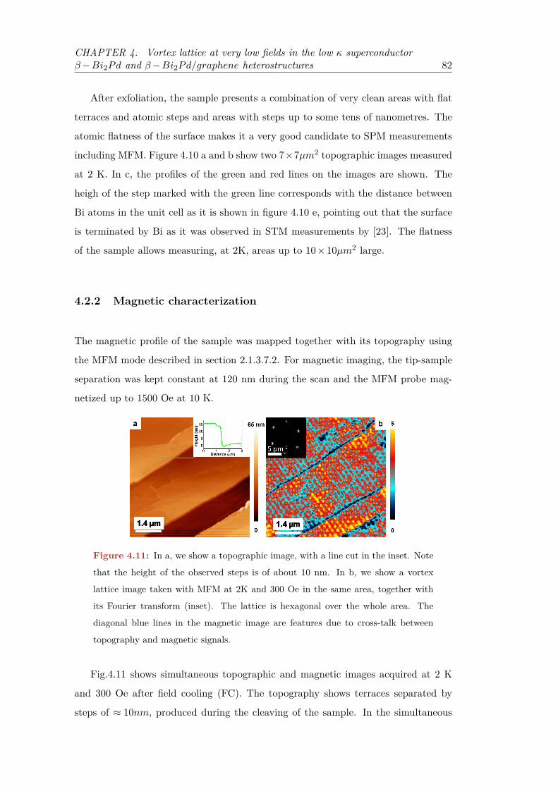
CHAPTER 4. Vortex lattice at very low fields in the low κ superconductorβ−Bi2Pd and β−Bi2Pd/graphene heterostructures 82
After exfoliation, the sample presents a combination of very clean areas with flat
terraces and atomic steps and areas with steps up to some tens of nanometres. The
atomic flatness of the surface makes it a very good candidate to SPM measurements
including MFM. Figure 4.10 a and b show two 7×7µm2 topographic images measured
at 2 K. In c, the profiles of the green and red lines on the images are shown. The
heigh of the step marked with the green line corresponds with the distance between
Bi atoms in the unit cell as it is shown in figure 4.10 e, pointing out that the surface
is terminated by Bi as it was observed in STM measurements by [23]. The flatness
of the sample allows measuring, at 2K, areas up to 10×10µm2 large.
4.2.2 Magnetic characterization
The magnetic profile of the sample was mapped together with its topography using
the MFM mode described in section 2.1.3.7.2. For magnetic imaging, the tip-sample
separation was kept constant at 120 nm during the scan and the MFM probe mag-
netized up to 1500 Oe at 10 K.
Figure 4.11: In a, we show a topographic image, with a line cut in the inset. Note
that the height of the observed steps is of about 10 nm. In b, we show a vortex
lattice image taken with MFM at 2K and 300 Oe in the same area, together with
its Fourier transform (inset). The lattice is hexagonal over the whole area. The
diagonal blue lines in the magnetic image are features due to cross-talk between
topography and magnetic signals.
Fig.4.11 shows simultaneous topographic and magnetic images acquired at 2 K
and 300 Oe after field cooling (FC). The topography shows terraces separated by
steps of ≈ 10nm, produced during the cleaving of the sample. In the simultaneous

CHAPTER 4. Vortex lattice at very low fields in the low κ superconductorβ−Bi2Pd and β−Bi2Pd/graphene heterostructures 83
magnetic signal a vortex lattice is observed over the complete scanned area. We
observe a hexagonal vortex lattice over the whole image. Dark blue contrast is also
seen in the magnetic images at the position of the topographic steps due to cross-talk
between topography and magnetic measurements at the steps [124, 179].
4.2.2.1 Evolution of the vortex lattice with the applied magnetic field
We report here too of measurements made elsewhere, using a SQUID on a tip (SOT)
set-up described in [180] and our MFM measurements. SOT measurements were done
always in FC conditions by Dr. Yonathan Anahory and Dr Lior Embon in the group
of Prof. Eli Zeldov at the Weizmann Institute in Israel with a tip-sample separation
of several microns.
The measurements at very low magnetic fields using SOT and at higher fields
with MFM provide a radically different behaviour. The vortex lattice is disordered
at the lowest fields and becomes gradually more ordered, reaching the hexagonal
arrangement for fields close to 100 Oe. Above this field, vortices always arrange
in a hexagonal lattice. Selected SOT and MFM images are shown in Figure 4.12.
From visual inspection it is clear that, at the lower fields, the vortices are randomly
arranged. Upon increasing the field, the flux line lattice becomes gradually more
ordered in a hexagonal arrangement, expected for Abrikosov flux line lattice as is
clearly seen in the images above 100 Oe.
To quantitatively describe the vortex distribution, Delaunay triangulation was
performed for all SOT and MFM images. In the SOT images, along the defects,
above H ≈ 10 Oe, we do not fully resolve isolated vortices. We have used the small
peaks observed in the local magnetic field profile to identify vortex positions. To
independently verify that the count is right, we have integrated the magnetic field
in the SOT images along the defects and verified that the resulting flux coincides
with expected value from the number of vortices we use in the triangulation. A few
images are shown in Fig. 4.13 as an example, together with a Delaunay triangulation
scheme.

CHAPTER 4. Vortex lattice at very low fields in the low κ superconductorβ−Bi2Pd and β−Bi2Pd/graphene heterostructures 84
Figure 4.12: Evolution of the vortex distribution in β−Bi2Pd with the applied
magnetic field. Images a-g were taken with SOT and present a disordered distri-
bution at the lowest field that becomes more orderer at higher fields, vortex accu-
mulation in clusters and linear features are observed. Images from h-l were taken
with MFM. A regular Abrikosov lattice is clearly shown in all images. The lattice
becomes denser as the magnetic field increases, as expected. The color scale repre-
sents the out-of-plane field, with span of 2 in a, 3.5 in b-c, 8.4 in d, 7.2 in e and 7.0
in f-g Oe in the SOT images and of 2 Degrees in the MFM images, h-l. The white
scale bar represents 1µm.
With a Delaunay triangulation, we identify, measuring the distances between
close-by vortices, the nearest neighbors of each vortex. These can be six, as in a
hexagonal lattice, or more or less, when the lattice is disordered. Using the Delaunay
triangulation, we can find the intervortex distances over the whole image and identify
positions with defects in the vortex lattice, as positions with a number of nearest
neighbors different from six.
The results of the triangulation are presented in in figure 4.14. The colour map
corresponds to the distribution of intervortex distances extracted from the Delaunay
triangulation. For fields below ∼ 100 Oe, the histogram broadens and the distances
between vortices become widespread. At very low magnetic fields we can observe
intervortex distances ranging between half and twice the expected intervortex distance
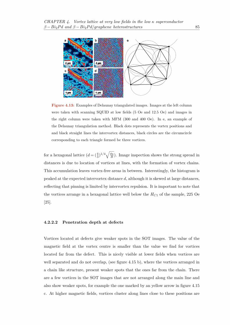
CHAPTER 4. Vortex lattice at very low fields in the low κ superconductorβ−Bi2Pd and β−Bi2Pd/graphene heterostructures 85
Figure 4.13: Examples of Delaunay triangulated images. Images at the left column
were taken with scanning SQUID at low fields (5 Oe and 12.5 Oe) and images in
the right column were taken with MFM (300 and 400 Oe). In e, an example of
the Delaunay triangulation method. Black dots represents the vortex positions and
and black straight lines the intervortex distances, black circles are the circumcircle
corresponding to each triangle formed be three vortices.
for a hexagonal lattice (d= (43)1/4
√φ0B ). Image inspection shows the strong spread in
distances is due to location of vortices at lines, with the formation of vortex chains.
This accumulation leaves vortex-free areas in between. Interestingly, the histogram is
peaked at the expected intervortex distance d, although it is skewed at large distances,
reflecting that pinning is limited by intervortex repulsion. It is important to note that
the vortices arrange in a hexagonal lattice well below the HC1 of the sample, 225 Oe
[25].
4.2.2.2 Penetration depth at defects
Vortices located at defects give weaker spots in the SOT images. The value of the
magnetic field at the vortex centre is smaller than the value we find for vortices
located far from the defect. This is nicely visible at lower fields when vortices are
well separated and do not overlap, (see figure 4.15 b), where the vortices arranged in
a chain like structure, present weaker spots that the ones far from the chain. There
are a few vortices in the SOT images that are not arranged along the main line and
also show weaker spots, for example the one marked by an yellow arrow in figure 4.15
c. At higher magnetic fields, vortices cluster along lines close to these positions are

CHAPTER 4. Vortex lattice at very low fields in the low κ superconductorβ−Bi2Pd and β−Bi2Pd/graphene heterostructures 86
Figure 4.14: Intervortex distances vs the applied magnetic field. The black line
represents the expected intervortex distance (d(nm) = (43 )1/4
√φ0B ), the red circles
the measured intervortex distances with the MFM and the colour map the distribu-
tion of probabilities of intervortex distances obtained with the triangulation of the
SOT images. Two different regimes are found, one at fields below HC1 ≈ 100 Oe,
where the vortex distribution is widespread and other above HC1 ≈ 100 Oe, where
the vortices are ordered forming the Abrikosov lattice. The lower critical field mea-
sured in [25] is represented by the green doted line. Colour scale is as represented
by the bar at the right. In the insets, the histograms obtained for 3 and 25 Oe.
found (figure 4.15 d). These vortices are thus also located close to a defect.
In the inset of Fig. 4.15 a we show magnetic field profiles along two vortices
showing weak and bright spots respectively. The profile of the isolated vortex can
be fitted to a monopole located at a distance λ+ dSOT from the SOT where λ is
the penetration depth and dSOT is the distance from the tip to the sample surface.
Since the value of lambda is known, λ = 132±20 nm [25], the value of dSOT can be
estimated for the brighter spot. This analysis was performed by Dr Anahory, who
left the penetration depth as a free parameter to fit the profile of the weak spots and
find λD = 270±40 nm which is about two times the value found elsewhere.
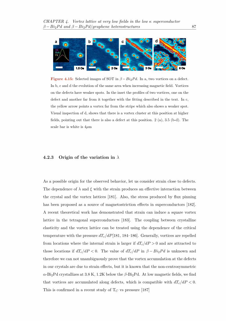
CHAPTER 4. Vortex lattice at very low fields in the low κ superconductorβ−Bi2Pd and β−Bi2Pd/graphene heterostructures 87
Figure 4.15: Selected images of SOT in β−Bi2Pd. In a, two vortices on a defect.
In b, c and d the evolution of the same area when increasing magnetic field. Vortices
on the defects have weaker spots. In the inset the profiles of two vortices, one on the
defect and another far from it together with the fitting described in the text. In c,
the yellow arrow points a vortex far from the stripe which also shows a weaker spot.
Visual inspection of d, shows that there is a vortex cluster at this position at higher
fields, pointing out that there is also a defect at this position. 2 (a), 3.5 (b-d). The
scale bar is white is 4µm
4.2.3 Origin of the variation in λ
As a possible origin for the observed behavior, let us consider strain close to defects.
The dependence of λ and ξ with the strain produces an effective interaction between
the crystal and the vortex lattices [181]. Also, the stress produced by flux pinning
has been proposed as a source of magnetostriction effects in superconductors [182].
A recent theoretical work has demonstrated that strain can induce a square vortex
lattice in the tetragonal superconductors [183]. The coupling between crystalline
elasticity and the vortex lattice can be treated using the dependence of the critical
temperature with the pressure dTc/dP [181, 184–186]. Generally, vortices are repelled
from locations where the internal strain is larger if dTc/dP > 0 and are attracted to
those locations if dTc/dP < 0. The value of dTc/dP in β−Bi2Pd is unknown and
therefore we can not unambiguously prove that the vortex accumulation at the defects
in our crystals are due to strain effects, but it is known that the non-centrosymmetric
α-Bi2Pd crystallizes at 3.8 K, 1.2K below the β-Bi2Pd. At low magnetic fields, we find
that vortices are accumulated along defects, which is compatible with dTc/dP < 0.
This is confirmed in a recent study of TC vs pressure [187]

CHAPTER 4. Vortex lattice at very low fields in the low κ superconductorβ−Bi2Pd and β−Bi2Pd/graphene heterostructures 88
4.2.4 Origin of the flux landscape
All our experiments are in field cooled conditions, so we quench, during cooling,
vortices at locations where the free energy landscape is more favourable [153–155, 162].
For the lowest magnetic fields, we find strong gradients in the vortex distribution. To
analyse this further, we calculate the elastic energy associated to pairs of vortices,
F , at different locations in our images. We compare the result for vortices located
at a defect and giving weak spots in SOT images, with the elastic energy for pairs of
vortices far from the defects. To this end, we use F = φ20
4πµ0λ2 log(κ) + φ20
4πµ0λ2K0(d/λ)
for the free energy per unit length of two vortices interacting with each other at a
distance d [28]. The first term comes from the energy of superfluid currents, giving
the line tension of the vortex, and the second term represents the interaction energy
between vortices. K0 is the modified Bessel function of the second kind. We then
calculate F for vortices far from defects using the bulk λ and for vortices at the
defects, using λD provided above. Below ≈ 50Oe the intervortex distances vary from
0.5 to 4 µm and the second term of the interaction energy remains negligible with
respect to the first term, giving a difference in free energy between both situations of
∆F ≈ 2×10⁻¹¹J/m3 independent of the intervortex distance.
We can now compare ∆F with the pinning energy of a vortex pinned at a normal
inclusion in β-Bi2Pd using Ucore = B2cπξ
2
µ0[188], with Bc the thermodynamic critical
field and ξ the superconducting coherence length (ξ ≈ 25 nm, [23, 189]). We find
a value which is smaller than ∆F , 1× 10⁻¹¹Jm−1. Thus, single vortex pinning at
defects play an unimportant role in the vortex distribution on β−Bi2Pd. Moreover,
it is difficult to think of normal inclusions as large as ξ≈ 25 nm to pin isolated vortices.
Thus, pinning seems to play a minor role in β-Bi2Pd at low fields. The accumulation
of vortices at the defects can be explained with the lower free energy caused by the
experimentally determined changes in λ.
It is quite remarkable that such a simple estimation provides such clear results,
and are probably particularly valid when vortices are very far apart, at the low-
est magnetic fields we have studied. For higher magnetic fields, the vortex lat-
tice density increases and the previous two-vortex interaction approximation is no
CHAPTER 4. Vortex lattice at very low fields in the low κ superconductorβ−Bi2Pd and β−Bi2Pd/graphene heterostructures 89
longer valid. For fields above ≈ 50 Oe we have considered the free energy of a vor-
tex, interacting with its first six neighbours arranged in a hexagonal lattice using:
F = nφ2
04πµ0λ2 log(κ) + 3n φ2
04πµ0λ2K0(a/λ) [28], where a is the lattice parameter of the
Abrikosov lattice determined by a= (43)1/4
(Φ0B
)1/2and n the number of vortices per
unit area. The difference of energy between six vortices close to a defect with λD
and six vortices far from the defect with λ changes with the intervortex distance. We
find that when vortices at the defect are closer than about 400 nm, it is no longer
energetically favourable to add new vortices to the defect. This can explain the vortex
distribution at low fields shown in Fig. 4.14. We find that the cross-over field is of
≈ 200 Oe. In the experiment, we find that already at ≈ 100Oe the distance histogram
closes and the vortex lattice becomes hexagonal. We believe that, given the crude
approximations made, the agreement is remarkable and provides a simple but useful
explanation to the vortex landscape at low fields.
It is also noteworthy that the average value of the intervortex distances follows d
for all magnetic fields. This finding has not been previously reported, to our knowl-
edge, at low magnetic fields and in presence of strongly inhomogeneous vortex distri-
butions. Instead the usual pictures consist of clusters of vortices with widely differing
intervortex distances that are often smaller than d.
The vortex patterns that we have measured in β-Bi2Pd showed both behaviours.
At very low fields, there are strong gradients in the vortex distribution. No stripes
or clusters as in MgB2 with two well defined intervortex distances, but nevertheless
strong vortex accumulation. At higher magnetic fields, still below Hc1, we observe in
contrast a hexagonal, defect free, vortex lattice.
β-Bi2Pd is clearly a single gap superconductor, so vortex clustering cannot be
associated to multiple gap opening here [23, 25]. Thus, the vortex patterns at very
low fields in β−Bi2Pd are due to the distortion of the hexagonal lattice formed during
the FC process by pinning at crystalline defects due to differences in the values of
the penetration depth. At very low fields, the vortex-vortex repulsion potential is
small, and pinning dominates, leading to the observed vortex clustering. At higher
fields, the vortex-vortex repulsion potential impedes pinning of isolated vortices and
the vortex lattice arranges as a whole in a regular hexagonal lattice.

CHAPTER 4. Vortex lattice at very low fields in the low κ superconductorβ−Bi2Pd and β−Bi2Pd/graphene heterostructures 90
It would be interesting to consider this scenario within the very recent proposal for
a small p-wave component appearing in the order parameter close to the surface [178].
Particularly close to defects, we can think of modifications in the surface properties
that could enhance such effects.
4.2.4.1 Evolution of the vortex lattice with the temperature
The penetration depth is expected to increase as the temperature approaches TC ,
therefore, the superconducting vortex profile will be broader as the temperature in-
creases. Eventually, at Tc, the magnetic profile will become homogeneous over the
whole surface of the superconductor [28, 190].
Figure 4.16: Evolution of the vortex lattice with the temperature. In the upper
panel, a plot of the evolution of the magnetic contrast with the temperature is shown.
The experimental data (black circles) was obtained from MFM images measured
under a perpendicular magnetic field of 300 Oe at the same area. The blue line
represents the expected magnetic contrast due to the theoretical evolution of λ
as explained in the text. Both curves have the same behavior, proving that the
evolution of the vortex width is dominated by the evolution of λ. In the lower panel,
four of the MFM images used to obtain the plot. Scale bar in white is 1µm.
We have measured the magnetic profile of the same area at different temperatures
CHAPTER 4. Vortex lattice at very low fields in the low κ superconductorβ−Bi2Pd and β−Bi2Pd/graphene heterostructures 91
and constant magnetic field. After cooling down the sample to 2.75 K in a perpen-
dicular magnetic field of 300 Oe, the temperature was increased to 3, 3.25, 3.5, 4, 4.5
and 5 K recording the magnetic profile at each temperature. The evolution of the
vortex profile width with the temperature is presented in figure 4.16. Experimental
data was obtained as the difference between the MFM signal at the centre of the vor-
tices and the background between vortices. The magnetic field profile around vortices
becomes broader as the temperature increases. This can be related to the increase
in the penetration depth, λ(T ) = λ(T=0)1−(T/TC)4 . In the image, the relation between the
experimental data and the expected evolution of the penetration depth is clear. We
have calculated the expected value of the contrast as the difference of the magnetic
field at the centre of a vortex and in between its neighbours in an hexagonal lattice
using equation 2.14. At 5 K, no vortex lattice was found in the sample, in agreement
with the resistive TC [23].
4.2.4.2 Orientation of the vortex lattice
Previous works in the same β−Bi2Pd crystals have found that at high fields, the
hexagonal vortex lattice is oriented with one of its axis along a crystallographic di-
rection [23]. AFM has no atomic resolution and therefore, it can not determine the
directions of the crystals lattice, but they can be inferred from the direction of the
atomic steps that are easily measured with an AFM.
Here, we have found that at low magnetic fields, below ≈ 200Oe, the vortex
lattice is preferentially oriented with one axis following the steps direction. At higher
magnetic fields, when the distances are practically homogeneous over the whole field
of view, the vortex lattice is oriented at 90 with respect to the defects (figure 4.17).
And it suggests that the vortex accumulation around defects found at the lowest fields
does not occur exactly at the pinning centers (which would favor that one of the main
axis of the hexagonal vortex lattice is oriented with the defect), but is a result of a
collective interaction between vortex and crystal lattices.

CHAPTER 4. Vortex lattice at very low fields in the low κ superconductorβ−Bi2Pd and β−Bi2Pd/graphene heterostructures 92
Figure 4.17: Example of the two vortex lattice orientations found. In a, the vortex
lattice at 200 Oe form ≈ 30 with respect to the topographic step (dashed black line
in the image). In b, at 300 Oe, one of the main directions of the vortex lattice is
normal to the topographic step. In both images the direction of the vortex lattice
is highlighted with a light blue line.
4.3 Electrochemical transfer of graphene on β-Bi2Pd
We have transfered a graphene sheet of ≈ 1 cm × 1 cm area on a β-Bi2Pd substrate
using a PMMA as a wetting layer. The graphene sheet was grown in high vacuum
on a copper foil by Jon Azpeitia at the laboratory of Prof. Jose Martin Gago (for a
detailed description of the graphene growth see references [192] and [193]).
To transfer the graphene sheet from the copper foil to the β-Bi2Pd substrate we
have used the common electrochemical transfer method described in [194, 195]. In
this method, first, the graphene is covered by a PMMA layer via spin coating (figure
4.18 a). Then, the coper foil with the graphene and the PMMA is immersed in a
solution of potassium chloride at a rate of 1 mm/s (figures 4.18 b and 4.19 a). The
copper is negatively polarized up to 5 V with respect to a carbon anode. When
the graphene/copper cathode is negatively polarized, hydrogen bubbles appear at the
graphene/copper interface due to the reduction of water molecules and allow graphene
to gently detach (figure 4.18 c). Then, the graphene/PMMA layer is placed on top
of the substrate (figures 4.18 d and 4.19 c) and the PMMA layer is dissolved with
acetone to obtain free graphene deposit on top of the substrate (figure 4.18 e and f).
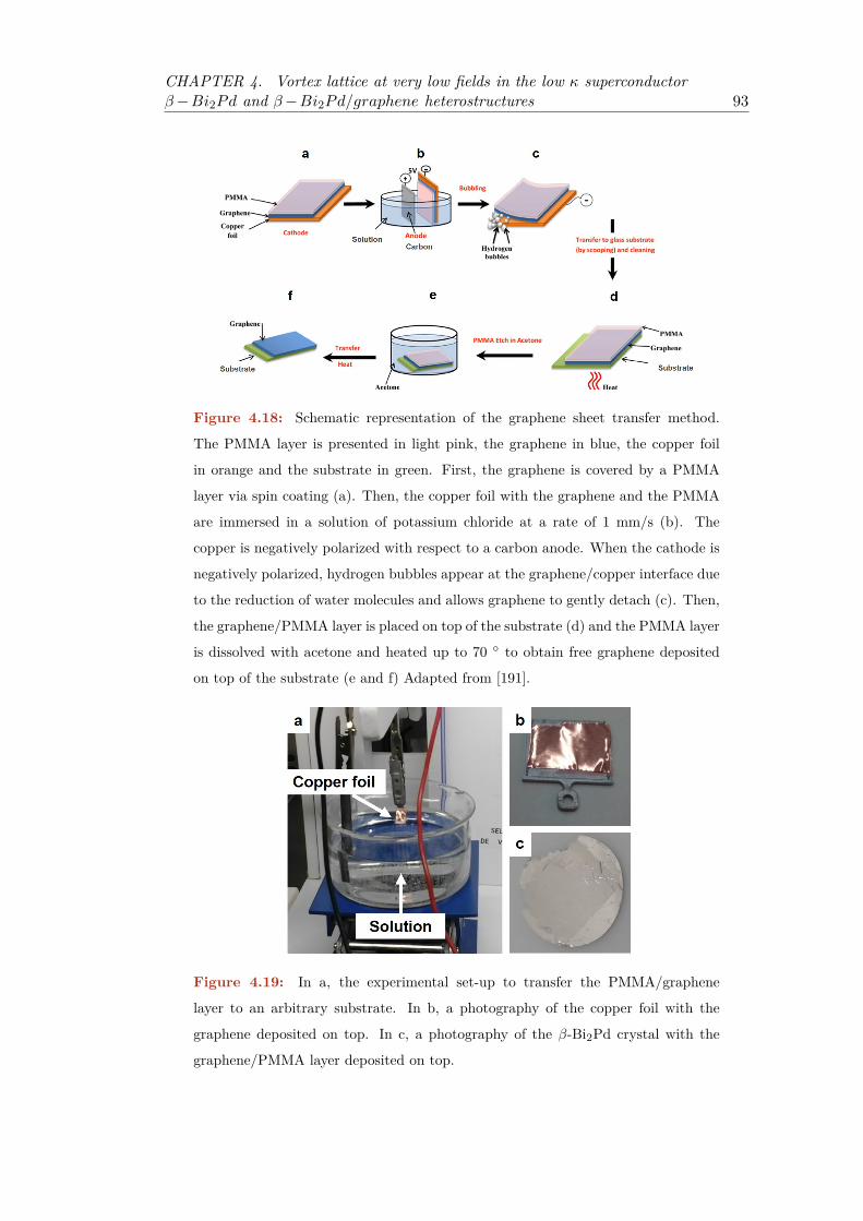
CHAPTER 4. Vortex lattice at very low fields in the low κ superconductorβ−Bi2Pd and β−Bi2Pd/graphene heterostructures 93
Figure 4.18: Schematic representation of the graphene sheet transfer method.
The PMMA layer is presented in light pink, the graphene in blue, the copper foil
in orange and the substrate in green. First, the graphene is covered by a PMMA
layer via spin coating (a). Then, the copper foil with the graphene and the PMMA
are immersed in a solution of potassium chloride at a rate of 1 mm/s (b). The
copper is negatively polarized with respect to a carbon anode. When the cathode is
negatively polarized, hydrogen bubbles appear at the graphene/copper interface due
to the reduction of water molecules and allows graphene to gently detach (c). Then,
the graphene/PMMA layer is placed on top of the substrate (d) and the PMMA layer
is dissolved with acetone and heated up to 70 to obtain free graphene deposited
on top of the substrate (e and f) Adapted from [191].
Figure 4.19: In a, the experimental set-up to transfer the PMMA/graphene
layer to an arbitrary substrate. In b, a photography of the copper foil with the
graphene deposited on top. In c, a photography of the β-Bi2Pd crystal with the
graphene/PMMA layer deposited on top.
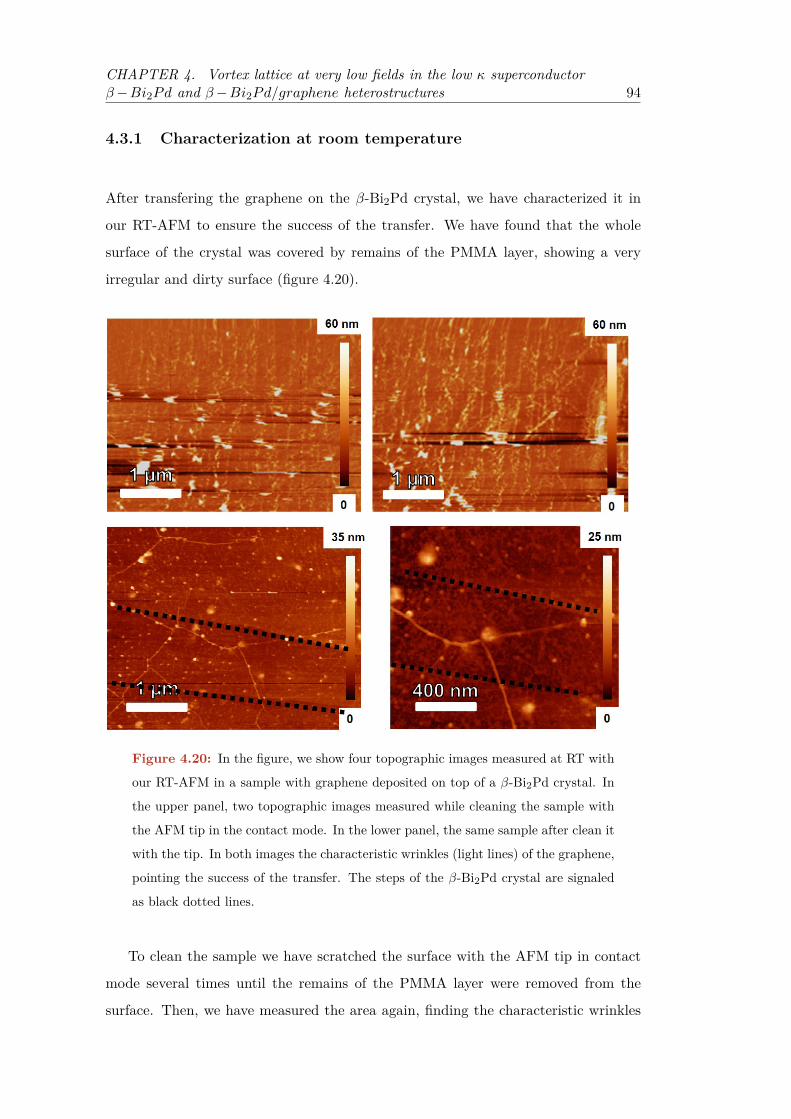
CHAPTER 4. Vortex lattice at very low fields in the low κ superconductorβ−Bi2Pd and β−Bi2Pd/graphene heterostructures 94
4.3.1 Characterization at room temperature
After transfering the graphene on the β-Bi2Pd crystal, we have characterized it in
our RT-AFM to ensure the success of the transfer. We have found that the whole
surface of the crystal was covered by remains of the PMMA layer, showing a very
irregular and dirty surface (figure 4.20).
Figure 4.20: In the figure, we show four topographic images measured at RT with
our RT-AFM in a sample with graphene deposited on top of a β-Bi2Pd crystal. In
the upper panel, two topographic images measured while cleaning the sample with
the AFM tip in the contact mode. In the lower panel, the same sample after clean it
with the tip. In both images the characteristic wrinkles (light lines) of the graphene,
pointing the success of the transfer. The steps of the β-Bi2Pd crystal are signaled
as black dotted lines.
To clean the sample we have scratched the surface with the AFM tip in contact
mode several times until the remains of the PMMA layer were removed from the
surface. Then, we have measured the area again, finding the characteristic wrinkles

CHAPTER 4. Vortex lattice at very low fields in the low κ superconductorβ−Bi2Pd and β−Bi2Pd/graphene heterostructures 95
of graphene in the whole field of view of the image (figure 4.20). There are also visible
some surface contaminations that remains at the surface after cleaning the system
with the tip. This measurements point the big success of the transfer.
4.3.2 Characterization at low temperatures
We have measured the same sample at low temperatures. Figure 4.21 shows the
topographic image of the sample at 2 K before and after cleaning it with the AFM
tip. We were able to clean the surface without damaging the graphene layer or the
MFM tip. Figure 4.21 reveals the characteristic wrinkles of the graphene layers and
some steps and terraces of the β-Bi2Pd crystal, showing the success of our cleaning
method at low temperatures.
Figure 4.21: In the figure, we show two topographic images measured at 2K with
our LT-AFM in a sample with graphene deposited on top of a β-Bi2Pd single crystal.
In the left panel, the area before cleaning it with the tip and in the right panel after
cleaning it. In this image are visible the characteristic wrinkles of the graphene
pointing the success of the transfer and cleaning methods.
After cleaning the surface, we have measured the magnetic field on the surface of
the sample. Figure 4.22 shows the topographic and magnetic images measured at the
same area at 2 K and under an applied magnetic field of 300 Oe in the out of plane
direction. The magnetic image shows a hexagonal vortex lattice in the whole field of
view, revealing that it is possible to observe the vortex lattice through the graphene
layer. From the image, we have not found any visible distortion of the hexagonal
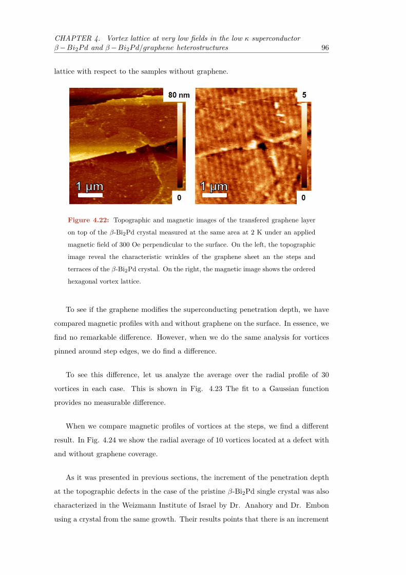
CHAPTER 4. Vortex lattice at very low fields in the low κ superconductorβ−Bi2Pd and β−Bi2Pd/graphene heterostructures 96
lattice with respect to the samples without graphene.
Figure 4.22: Topographic and magnetic images of the transfered graphene layer
on top of the β-Bi2Pd crystal measured at the same area at 2 K under an applied
magnetic field of 300 Oe perpendicular to the surface. On the left, the topographic
image reveal the characteristic wrinkles of the graphene sheet an the steps and
terraces of the β-Bi2Pd crystal. On the right, the magnetic image shows the ordered
hexagonal vortex lattice.
To see if the graphene modifies the superconducting penetration depth, we have
compared magnetic profiles with and without graphene on the surface. In essence, we
find no remarkable difference. However, when we do the same analysis for vortices
pinned around step edges, we do find a difference.
To see this difference, let us analyze the average over the radial profile of 30
vortices in each case. This is shown in Fig. 4.23 The fit to a Gaussian function
provides no measurable difference.
When we compare magnetic profiles of vortices at the steps, we find a different
result. In Fig. 4.24 we show the radial average of 10 vortices located at a defect with
and without graphene coverage.
As it was presented in previous sections, the increment of the penetration depth
at the topographic defects in the case of the pristine β-Bi2Pd single crystal was also
characterized in the Weizmann Institute of Israel by Dr. Anahory and Dr. Embon
using a crystal from the same growth. Their results points that there is an increment
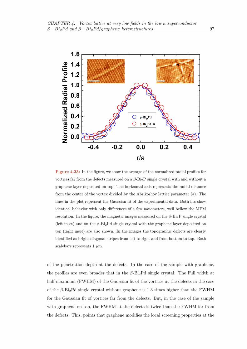
CHAPTER 4. Vortex lattice at very low fields in the low κ superconductorβ−Bi2Pd and β−Bi2Pd/graphene heterostructures 97
Figure 4.23: In the figure, we show the average of the normalized radial profiles for
vortices far from the defects measured on a β-Bi2P single crystal with and without a
graphene layer deposited on top. The horizontal axis represents the radial distance
from the center of the vortex divided by the Abrikoshov lattice parameter (a). The
lines in the plot represent the Gaussian fit of the experimental data. Both fits show
identical behavior with only differences of a few nanometers, well bellow the MFM
resolution. In the figure, the magnetic images measured on the β-Bi2P single crystal
(left inset) and on the β-Bi2Pd single crystal with the graphene layer deposited on
top (right inset) are also shown. In the images the topographic defects are clearly
identified as bright diagonal stripes from left to right and from bottom to top. Both
scalebars represents 1 µm.
of the penetration depth at the defects. In the case of the sample with graphene,
the profiles are even broader that in the β-Bi2Pd single crystal. The Full width at
half maximum (FWHM) of the Gaussian fit of the vortices at the defects in the case
of the β-Bi2Pd single crystal without graphene is 1.3 times higher than the FWHM
for the Gaussian fit of vortices far from the defects. But, in the case of the sample
with graphene on top, the FWHM at the defects is twice than the FWHM far from
the defects. This, points that graphene modifies the local screening properties at the

CHAPTER 4. Vortex lattice at very low fields in the low κ superconductorβ−Bi2Pd and β−Bi2Pd/graphene heterostructures 98
defects of the β-Bi2Pd single crystal and produces and enhancement of the penetration
depth at these positions.
Figure 4.24: In the figure, we show the average of the normalized radial profiles
for vortices at the defects measured on a β-Bi2P single crystal with and without a
graphene layer deposited on top. The horizontal axis represents the radial distance
from the center of the vortex divided by the Abrikoshov lattice parameter (a). The
lines in the plot represent the Gaussian fit of the experimental data. In the figure,
the magnetic images measured on the β-Bi2P single crystal (left inset) and on the
β-Bi2Pd single crystal with the graphene layer deposited on top (right inset) are
also shown. In the images the topographic defects are clearly identified as bright
diagonal stripes from left to right and from bottom to top. Both scalebars represents
1 µm.
Thus, graphene does not modify the magnetic flux out of the superconductor
when there are no defects. As in the tunneling experiments shown in Ref. [102] in
Re, graphene is strongly coupled to the substrate and essentially it is transparent,
and remains superconducting, for all practical purposes.
At the defects, however, there is a clear increase in the penetration depth produced

CHAPTER 4. Vortex lattice at very low fields in the low κ superconductorβ−Bi2Pd and β−Bi2Pd/graphene heterostructures 99
by the graphene layer. This effect can be explained by an increase in the distance
between graphene and the surface at the step edges. This decreases the barrier
Γ, providing thus a reduction of the superconducting gap induced in graphene and
therefore an increase in the penetration depth.
Several theoretical works have proposed different mechanism of superconductivity
in graphene by placing it on a superconductor with a BCS or a non-BCS pairing sym-
metry [96, 97], depending on the position of the Fermi level with respect to the Dirac
point. Experimentally, superconductivity in graphene was achieved by placing it in
contact with the s-wave superconductor Re and the superconductor Pr2−xCexCuO4
[2]. In the case of β-Bi2Pd, a recent work, has proposed the existence of topological
p-wave superconductivity at the surface [178] in addition of the previously reported
s-wave behavior at the bulk [24, 25].
4.4 Summary and conclusions
In conclusion, we have observed two different regimes in the patterns of pinned super-
conducting vortices at low magnetic fields in the single gap superconductor β-Bi2Pd.
We have shown that lines of vortices form at defects due to pinning at very low mag-
netic fields, while at higher fields the vortex lattice acts as a whole, showing a regular
hexagonal lattice even below Hc1. Crystalline strain close to defects determines the
vortex arrangements at low fields and leads to sizable modifications of the local su-
perconducting screening properties. The mutual influence of crystalline strain and
the vortex lattice has been extensively studied at high magnetic fields. Here, we show
that this mutual influence also modifies vortex arrangements at very low magnetic
fields. At fields slightly aboveHC1, where vortices are arranged in a regular Abrikosov
lattice, we have found that the magnetic profile of the vortices follow the expected
behaviour when changing the temperature. We have not found any evidence of vortex
clustering when decreasing the temperature as in other superconducting materials.
Instead, there is a widespread distribution of intervortex distances.
Finally, we have transfered a ≈ 1 cm × 1 cm graphene sheet on top of a β-Bi2Pd

CHAPTER 4. Vortex lattice at very low fields in the low κ superconductorβ−Bi2Pd and β−Bi2Pd/graphene heterostructures 100
single crystal with the electrochemical transfer method and measured the vortex
lattice of the β-Bi2Pd crystal at the superconducting state at 2K trough the graphene
layer. We have not found any difference between the magnetic profile of vortices
far from the topographic defects in the β-Bi2Pd crystal between the sample with
and without graphene on top. We have found that in the case of the sample with
graphene on top, vortices become much broader at the position of the topographic
defects in the β-Bi2Pd crystal than in the case of vortices in the sample without
graphene. This experiment demonstrates that graphene is essentially transparent for
the magnetic properties of superconductivity, unless the interaction between sample
and substrate is modified. When the interaction is weaker, we observe that the
penetration depth increases, opening the path to interesting experiments addressing
unconventional superconducting properties.

CHAPTER 5
Strain induced magneto-structural and
superconducting transitions in
Ca(Fe0.965Co0.35)2As2
Tuning parameters are a essential tool in the study of materials, since they can be
used to control the appearance of an specific behavior. As an example, unconventional
superconductivity often emerges around the point where antiferromagnetic order is
suppressed by hydrostatic pressure [196]. Strain has been occasionally used as a
tuning parameter [197–200], but is less employed than pressure. Strain has been
mostly employed to probe the nematic susceptibility of iron-based superconductors
[201–204].
Iron-based superconductors have a rich interplay between antiferromagnetism, or-
thorhombic to tetragonal distortion and superconductivity. Numerous tuning param-
eters have been used in iron-based superconductors, including: chemical substitution
[205], hydrostatic pressure [206, 207], epitaxial strains in thin films [208, 209], uniaxial
strain in CaFe2As2 and BaFe2As2 [210–215] and biaxial pressure in Ca(Fe1−xCox)2As2[71].
101

CHAPTER 5. Strain induced magneto-structural and superconducting transitionsin Ca(Fe0.965Co0.35)2As2 102
5.1 Previous studies in the parent compound CaFe2As2
The parent compound, CaFe2As2, presents tetragonal structure together with param-
agnetism at ambient conditions and transits to either an antiferromagnetic/orthorhombic
(AFM/ORTH) phase or a paramagnetic/collapsed tetragonal (PM/CT) phase when
decreasing the temperature, depending on the hydrostatic pressure [216]. The AFM/ORTH
transition is also present on other compounds of the same family like BaFe2As2, but
CaFe2As2 is extremely sensitive to the pressure. For example it transits from or-
thorhombic to a collapsed tetragonal phase under 0.35 GPa at 33 K [216], which is a
much more moderated pressure than BaFe2As2 (29 GPa [217]).
Figure 5.1: Phase diagram of CaFe2As2 as a function of the post growth anneal-
ing temperature and the hydrostatic pressure. In the lower x-axis, the annealing
temperature and in the upper x-axis, the hydrostatic pressure. Black asterisks are
the pressure data measured in [216] and red circles are the data obtained from the
annealing treatment in [218]. Green and blue lines are a guide to the eye. Adapted
from [219].
The possibility of stabilizing the PM/CT ground state at ambient pressure was
also proved in [218] using a post growth annealing treatment. They argued that the
changes in the internal strains due to the formation of FeAs nanoparticles in the
sample are the cause of the change in the ground state as a function of the annealing
temperature. Changing the annealing temperature will modify the size of the FeAs
CHAPTER 5. Strain induced magneto-structural and superconducting transitionsin Ca(Fe0.965Co0.35)2As2 103
precipitates and therefore the internal strain. The combination of the phase diagrams
obtained in [216] and [218] is shown in figure 5.1. Authors establish, through this
work, a relationship between pressure and annealing temperature that is quite useful
to access some parts of the phase diagram using techniques where no pressure can be
applied.
5.1.1 Structural domains at low temperatures
Studies of polarized light microscopy have shown the formation of structural domains
below the tetragonal to orthorhombic transition in AFe2As2, A= Ca, Sr, Ba [220]. The
authors of this work associate the contrast of the optical images to the rotation of the
polarization plane between neighbouring domains in twin boundaries of orthorhombic
domains.
In figure 5.2 we show an optical image of a CaFe2As2 single crystal at 5 K,
well below the tetragonal to orthorhombic transition. A regular pattern of domain
boundaries oriented in two orthogonal directions is clearly visible. A typical domain
width is about 10 µm. Over large areas, sometimes covering the whole surface of the
crystal, domains form stacks of parallel plates. In some areas perpendicular domain
sets interpenetrate. The crystal under study has terraces on the sample surface and
shown in inset at RT, with a step size of the order of 20 µm. On crossing the
terraces, the domain lines perfectly match at different levels. This clearly shows that
the domain walls are extended along the c axis.
5.2 Previous studies in Ca(Fe1−xCox)2As2
A different approach was made by authors in [221]: they combined the effect of
cobalt substitution and post growth annealing to characterize the 3D phase diagram of
Ca(Fe1−xCox)2As2 as a function of these two tuning parameters. In Ca(Fe1−xCox)2As2,
substitution of Fe for Co suppresses a coupled of first-order magnetostructural tran-
sition at Ts,N and induces superconductivity with a maximum Tc of 16 K [221].
Authors in [221] proved that the ground state of Ca(Fe1−xCox)2As2 can be tuned to
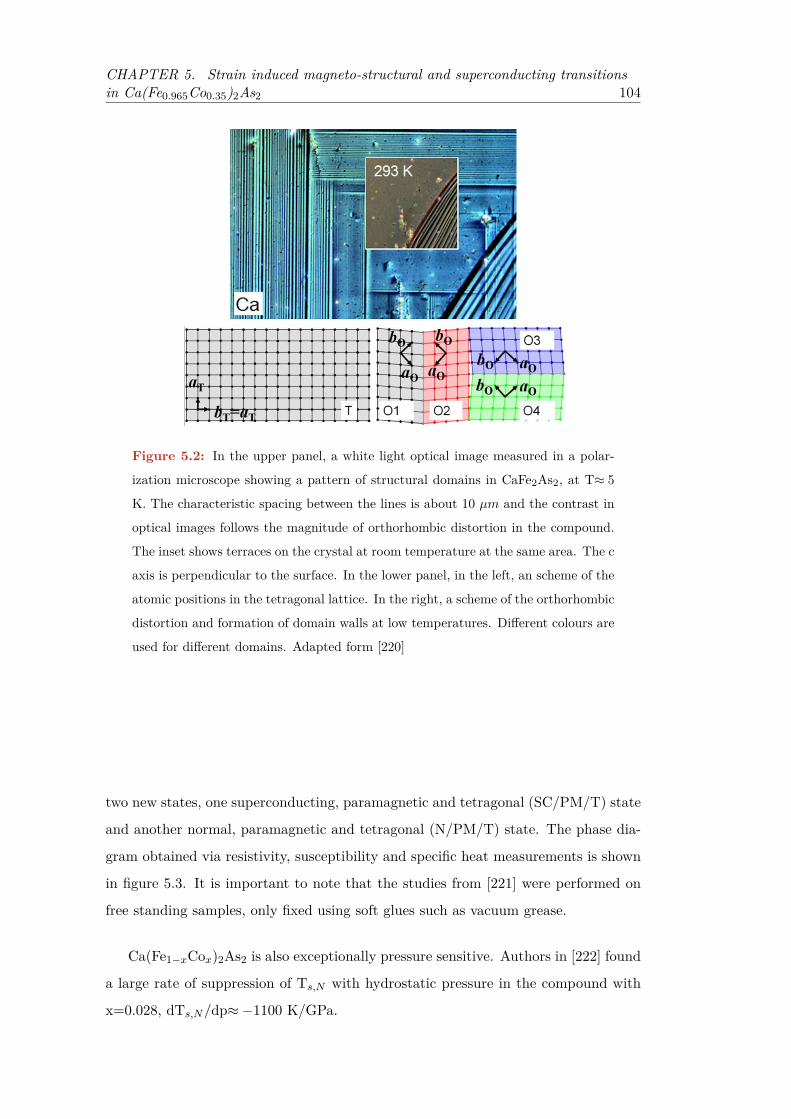
CHAPTER 5. Strain induced magneto-structural and superconducting transitionsin Ca(Fe0.965Co0.35)2As2 104
Figure 5.2: In the upper panel, a white light optical image measured in a polar-
ization microscope showing a pattern of structural domains in CaFe2As2, at T≈ 5
K. The characteristic spacing between the lines is about 10 µm and the contrast in
optical images follows the magnitude of orthorhombic distortion in the compound.
The inset shows terraces on the crystal at room temperature at the same area. The c
axis is perpendicular to the surface. In the lower panel, in the left, an scheme of the
atomic positions in the tetragonal lattice. In the right, a scheme of the orthorhombic
distortion and formation of domain walls at low temperatures. Different colours are
used for different domains. Adapted form [220]
two new states, one superconducting, paramagnetic and tetragonal (SC/PM/T) state
and another normal, paramagnetic and tetragonal (N/PM/T) state. The phase dia-
gram obtained via resistivity, susceptibility and specific heat measurements is shown
in figure 5.3. It is important to note that the studies from [221] were performed on
free standing samples, only fixed using soft glues such as vacuum grease.
Ca(Fe1−xCox)2As2 is also exceptionally pressure sensitive. Authors in [222] found
a large rate of suppression of Ts,N with hydrostatic pressure in the compound with
x=0.028, dTs,N/dp≈−1100 K/GPa.
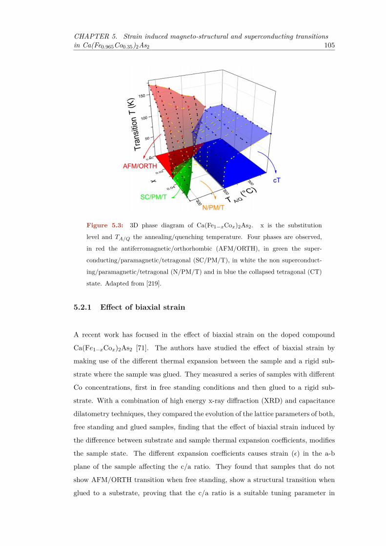
CHAPTER 5. Strain induced magneto-structural and superconducting transitionsin Ca(Fe0.965Co0.35)2As2 105
Figure 5.3: 3D phase diagram of Ca(Fe1−xCox)2As2. x is the substitution
level and TA/Q the annealing/quenching temperature. Four phases are observed,
in red the antiferromagnetic/orthorhombic (AFM/ORTH), in green the super-
conducting/paramagnetic/tetragonal (SC/PM/T), in white the non superconduct-
ing/paramagnetic/tetragonal (N/PM/T) and in blue the collapsed tetragonal (CT)
state. Adapted from [219].
5.2.1 Effect of biaxial strain
A recent work has focused in the effect of biaxial strain on the doped compound
Ca(Fe1−xCox)2As2 [71]. The authors have studied the effect of biaxial strain by
making use of the different thermal expansion between the sample and a rigid sub-
strate where the sample was glued. They measured a series of samples with different
Co concentrations, first in free standing conditions and then glued to a rigid sub-
strate. With a combination of high energy x-ray diffraction (XRD) and capacitance
dilatometry techniques, they compared the evolution of the lattice parameters of both,
free standing and glued samples, finding that the effect of biaxial strain induced by
the difference between substrate and sample thermal expansion coefficients, modifies
the sample state. The different expansion coefficients causes strain (ε) in the a-b
plane of the sample affecting the c/a ratio. They found that samples that do not
show AFM/ORTH transition when free standing, show a structural transition when
glued to a substrate, proving that the c/a ratio is a suitable tuning parameter in
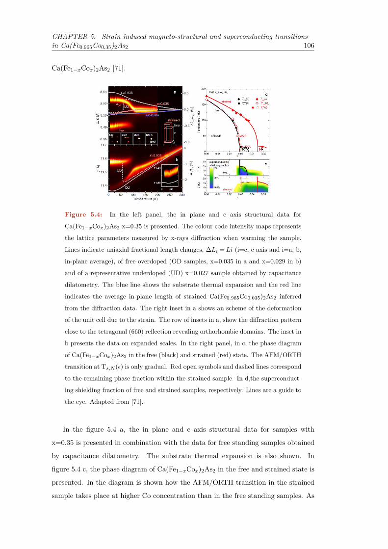
CHAPTER 5. Strain induced magneto-structural and superconducting transitionsin Ca(Fe0.965Co0.35)2As2 106
Ca(Fe1−xCox)2As2 [71].
Figure 5.4: In the left panel, the in plane and c axis structural data for
Ca(Fe1−xCox)2As2 x=0.35 is presented. The colour code intensity maps represents
the lattice parameters measured by x-rays diffraction when warming the sample.
Lines indicate uniaxial fractional length changes, ∆Li = Li (i=c, c axis and i=a, b,
in-plane average), of free overdoped (OD samples, x=0.035 in a and x=0.029 in b)
and of a representative underdoped (UD) x=0.027 sample obtained by capacitance
dilatometry. The blue line shows the substrate thermal expansion and the red line
indicates the average in-plane length of strained Ca(Fe0.965Co0.035)2As2 inferred
from the diffraction data. The right inset in a shows an scheme of the deformation
of the unit cell due to the strain. The row of insets in a, show the diffraction pattern
close to the tetragonal (660) reflection revealing orthorhombic domains. The inset in
b presents the data on expanded scales. In the right panel, in c, the phase diagram
of Ca(Fe1−xCox)2As2 in the free (black) and strained (red) state. The AFM/ORTH
transition at Ts,N (ε) is only gradual. Red open symbols and dashed lines correspond
to the remaining phase fraction within the strained sample. In d,the superconduct-
ing shielding fraction of free and strained samples, respectively. Lines are a guide to
the eye. Adapted from [71].
In the figure 5.4 a, the in plane and c axis structural data for samples with
x=0.35 is presented in combination with the data for free standing samples obtained
by capacitance dilatometry. The substrate thermal expansion is also shown. In
figure 5.4 c, the phase diagram of Ca(Fe1−xCox)2As2 in the free and strained state is
presented. In the diagram is shown how the AFM/ORTH transition in the strained
sample takes place at higher Co concentration than in the free standing samples. As
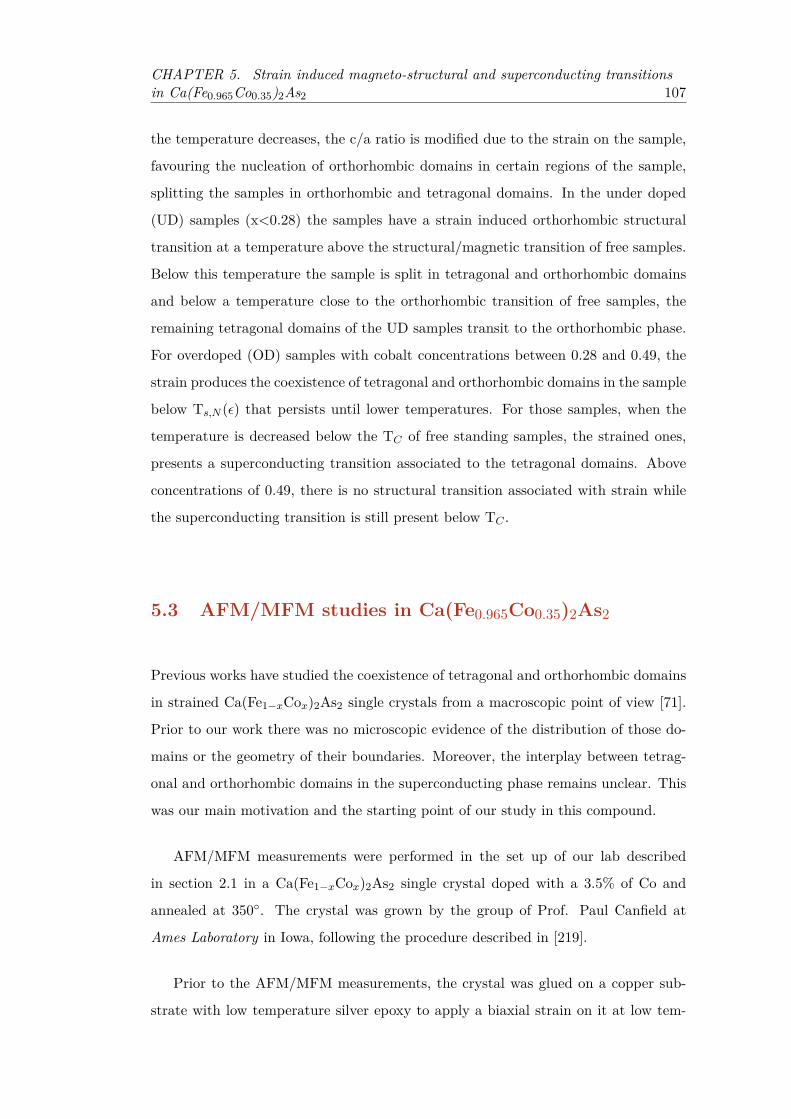
CHAPTER 5. Strain induced magneto-structural and superconducting transitionsin Ca(Fe0.965Co0.35)2As2 107
the temperature decreases, the c/a ratio is modified due to the strain on the sample,
favouring the nucleation of orthorhombic domains in certain regions of the sample,
splitting the samples in orthorhombic and tetragonal domains. In the under doped
(UD) samples (x<0.28) the samples have a strain induced orthorhombic structural
transition at a temperature above the structural/magnetic transition of free samples.
Below this temperature the sample is split in tetragonal and orthorhombic domains
and below a temperature close to the orthorhombic transition of free samples, the
remaining tetragonal domains of the UD samples transit to the orthorhombic phase.
For overdoped (OD) samples with cobalt concentrations between 0.28 and 0.49, the
strain produces the coexistence of tetragonal and orthorhombic domains in the sample
below Ts,N (ε) that persists until lower temperatures. For those samples, when the
temperature is decreased below the TC of free standing samples, the strained ones,
presents a superconducting transition associated to the tetragonal domains. Above
concentrations of 0.49, there is no structural transition associated with strain while
the superconducting transition is still present below TC .
5.3 AFM/MFM studies in Ca(Fe0.965Co0.35)2As2
Previous works have studied the coexistence of tetragonal and orthorhombic domains
in strained Ca(Fe1−xCox)2As2 single crystals from a macroscopic point of view [71].
Prior to our work there was no microscopic evidence of the distribution of those do-
mains or the geometry of their boundaries. Moreover, the interplay between tetrag-
onal and orthorhombic domains in the superconducting phase remains unclear. This
was our main motivation and the starting point of our study in this compound.
AFM/MFM measurements were performed in the set up of our lab described
in section 2.1 in a Ca(Fe1−xCox)2As2 single crystal doped with a 3.5% of Co and
annealed at 350. The crystal was grown by the group of Prof. Paul Canfield at
Ames Laboratory in Iowa, following the procedure described in [219].
Prior to the AFM/MFM measurements, the crystal was glued on a copper sub-
strate with low temperature silver epoxy to apply a biaxial strain on it at low tem-

CHAPTER 5. Strain induced magneto-structural and superconducting transitionsin Ca(Fe0.965Co0.35)2As2 108
peratures, similarly to the experiment in [71]. The same sample was also measured
with STM at the Laboratorio de Bajas Temperaturas de la Universidad Autonoma de
Madrid (LBTUAM) by Dr. Anton Fente in a set-up similar to the one described in
[223]. Some of his STM results will be presented together with the AFM/MFM mea-
surements to complement them, but the specifics of the STM experiments will not
be given here as they are beyond the scope of this thesis. It is important to empha-
size, that the sample was never unglued from the copper substrate, neither between
AFM/MFM experiments, neither to perform the STM measurement. Therefore, the
strain on the sample should be the same in the AFM/MFM and the STM measure-
ments.
A relevant difference between STM and AFM/MFM is that the surface needs to
be pristine to make STM measurements, whereas AFM/MFM measurements can be
made on surfaces that have been exposed to air. Therefore, the sample was first
inserted into the STM, cleaved in-situ in cryogenic vacuum, STM measurements were
made and then we measured it with the AFM/MFM. Furthermore, in our set-up we
can easily reach temperatures of 100 K and above, whereas the STM is optimized
for working below 4 K. Therefore, we could trace the temperature dependence much
better with the AFM system.
5.3.1 Topographic characterization
Topographic measurements were taken using the AFM dynamic mode described in
section 2.1.3.7.1 with typical tip-sample separation around 10 nm.
Very flat surfaces were easily found after cleaving the sample, making possible
topographic and magnetic images at 2 K up to ≈ 15×15µm2 with height differences
of tens of nanometres. The cleaving of the surface is expected to occur in the c-axis
[72]. An example of the crystal surface is presented in figure 5.5 together with a
topographic profile, and the unit cell of the crystal.
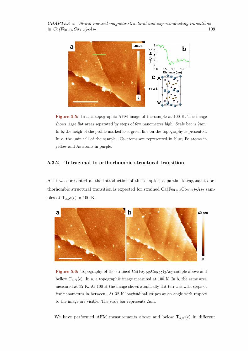
CHAPTER 5. Strain induced magneto-structural and superconducting transitionsin Ca(Fe0.965Co0.35)2As2 109
Figure 5.5: In a, a topographic AFM image of the sample at 100 K. The image
shows large flat areas separated by steps of few nanometres high. Scale bar is 2µm.
In b, the heigh of the profile marked as a green line on the topography is presented.
In c, the unit cell of the sample. Ca atoms are represented in blue, Fe atoms in
yellow and As atoms in purple.
5.3.2 Tetragonal to orthorhombic structural transition
As it was presented at the introduction of this chapter, a partial tetragonal to or-
thorhombic structural transition is expected for strained Ca(Fe0.965Co0.35)2As2 sam-
ples at Ts,N (ε)≈ 100 K.
Figure 5.6: Topography of the strained Ca(Fe0.965Co0.35)2As2 sample above and
bellow Ts,N (ε). In a, a topographic image measured at 100 K. In b, the same area
measured at 32 K. At 100 K the image shows atomically flat terraces with steps of
few nanometres in between. At 32 K longitudinal stripes at an angle with respect
to the image are visible. The scale bar represents 2µm.
We have performed AFM measurements above and below Ts,N (ε) in different
CHAPTER 5. Strain induced magneto-structural and superconducting transitionsin Ca(Fe0.965Co0.35)2As2 110
areas of the sample, finding radically different topographies. Above Ts,N (ε), in the
tetragonal phase, flat terraces and small steps of few nanometres were found (figure
5.6 a). Slightly below the structural transition expected from [71], we have observed
clear stripes in the topographic images (figure 5.6 b). The stripes are separated by
flat regions, few microns wide and are straight and parallel on the whole field of view.
The origin of the stripes will be discussed in the following.
5.3.2.1 Origin of the topographic stripes
The corrugation observed reminds AFM measurements below the tetragonal to or-
thorhombic transition in BaTiO3 [224] and STM measurement below the Verwey
transition in FeO3 [225]. In both materials, the corrugation in the surface was asso-
ciated to the reorientation of the structural domains due to the changes in the lattice
parameters in the transition. We believe that our images can be explained in the
same way.
The samples that present coexistence between orthorhombic and tetragonal do-
mains, have domain boundaries separating both phases and different orientations of
the same phase [71]. In the orthorhombic phase, the short axis, bORTH , is equal
to the lattice parameter of the tetragonal phase, aTET and therefore, the tetrago-
nal/orthorhombic domain boundary will occur along the crystallographic direction
determined by bORTH . Note in particular that the interface between these domains
has no stress within the plane, because in-plane lattice constants coincide along the
interface [71]. Domain boundaries between orthorhombic domains are in contrast,
oriented at 45 with respect to the crystallographic axis, forming a twin boundary
similar to the case of the parent compound CaFe2As2 described before [220]. In fig-
ure 5.7 two examples of the orthorhombic/tetragonal and orthorhombic/orthorhombic
domain walls are presented.
We now will introduce a simple model originally developed to explain the corru-
gation in BaTiO3 single crystals[226].
A condition for the formation of domain walls, is the matching and continuity of

CHAPTER 5. Strain induced magneto-structural and superconducting transitionsin Ca(Fe0.965Co0.35)2As2 111
Figure 5.7: Example of the structural domain boundaries in strained
Ca(Fe1−xCox)2As2. In the left panel, two domain boundaries between two or-
thorhombic and a tetragonal domain, the domain boundary develops along the crys-
tallographic direction determined by bORTH . In the right panel, the boundary be-
tween two orthorhombic domains, forming 45 with respect to the crystallographic
axis. Different colours are used for different crystallographic domains. The domain
wall is represented as a red line. Adapted from [72, 220].
the lattice at the wall [226]. Due to the differences in the c-axis lattice parameter
between the two phases below Ts,N in our crystal, this condition is fulfilled by the
accommodation of the tetragonal and orthorhombic domains schematically shown
in figure 5.8. The angle formed by the perpendicular and in-plane axis of both
lattices at each side of the wall is not exactly 90. It differs from 90 by an angle
α =arctan(ctet/atet)+arctan(aort/cort) [226]. We have calculated the expected angle
of the corrugation at the tet/orth domain wall using the lattice parameters obtained
for strained samples from [71]. We have found a corrugation angle of α≈ 0.55.
Topographic features in form of stripes were also measured in STM experiments
in the same sample (figure 5.9). In this case, the stripes are separated by tens of
nanometres and are few Angstroms high. The STM measurements also show the
2x1 reconstruction of Ca atoms expected for CaFe2As2 [72, 227] covering most of
the surface. The two main axis of the Ca reconstruction (corresponding to the two
main axis of the Ca sublattice) form 45 with the crystallographic axis [189]. As is
shown in figure 5.9, the reconstruction is found forming 45 with the topographic
stripes (vertical lines in the figure), thus the stripes are oriented in the direction of
the crystallographic axis. As it was presented in the introduction of the chapter,
the domain boundary compatible with a direction of the crystallographic axis is the

CHAPTER 5. Strain induced magneto-structural and superconducting transitionsin Ca(Fe0.965Co0.35)2As2 112
Figure 5.8: Scheme of the corrugation below the structural transition. The or-
thorhombic and tetragonal unit cells are represented in blue and yellow rectangles
respectively. The unit cell at the interface is represented as a grey polygon.
tetragonal/orthorhombic domain wall, with the domain parallel to the aTET and
bORTH axis. This shows that stripes reflect the tet/orth domain boundaries.
Figure 5.9: In the left panel, an STM topographic image taken at T<4.2K. The
image display parallel elongated stripes, forming 45 with the 2x1 Ca reconstruc-
tion. The white scale bar represents 100 nm. In the right panel, a schematized
tetragonal/orthorhombic domain wall. The 2x1 Ca reconstruction is marked with
by black arrows and different domains are represented by different colours.
We have calculated the angle between domains at both sides of the stripes in AFM
and STM images, finding that it remains almost constant in all the stripes with a
value between 0.8 and 1.3. A few STM and AFM selected images are shown together
with their topographic profiles and the measured angle at the stripes in figure 5.10.
It is noticeable that images with such different scales, present the same angle between
domains.
The value of the angle measured at the stripes is larger than the calculated angle

CHAPTER 5. Strain induced magneto-structural and superconducting transitionsin Ca(Fe0.965Co0.35)2As2 113
Figure 5.10: In the left column, thee topographic images measured by STM (a) and
AFM (c and e). The images, show step-like features associated to the tetragonal-
orthorhombic domain boundaries. In the right column, three topographic profiles
measured black lines on the topographic images. All the step-like features showed
in the profiles present an angle of ≈1 between the tetragonal and the orthorhombic
domains. The surface of the tetragonal and orthorhombic domains is highlighted in
the profiles using a blue and a red line respectively.
for this system (≈ 0.55). But it is important to note that the distortion of the
tetragonal and orthorhombic lattice is dependent on the strain and therefore on the
substrate where the sample is glued. We have followed a similar procedure as in
reference [71]. Thus, we can not unambiguously determine the magnitude of the
distortion of the unit cells in our crystal. Moreover, the model used to calculate the
distortion of the lattice at the boundary proposed in [226] is very simple. It assumes
that the unit cell at the boundary is deformed, presenting exactly the same cell
parameters of the tetragonal and orthorhombic phases at each side of the boundary,
which does not have to be exactly true. For example, small deviation of ≈ 0.5% from
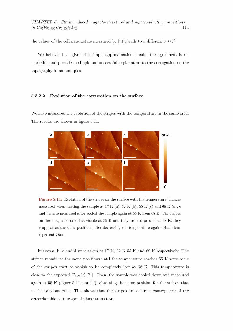
CHAPTER 5. Strain induced magneto-structural and superconducting transitionsin Ca(Fe0.965Co0.35)2As2 114
the values of the cell parameters measured by [71], leads to a different α≈ 1.
We believe that, given the simple approximations made, the agreement is re-
markable and provides a simple but successful explanation to the corrugation on the
topography in our samples.
5.3.2.2 Evolution of the corrugation on the surface
We have measured the evolution of the stripes with the temperature in the same area.
The results are shown in figure 5.11.
Figure 5.11: Evolution of the stripes on the surface with the temperature. Images
measured when heating the sample at 17 K (a), 32 K (b), 55 K (c) and 68 K (d), e
and f where measured after cooled the sample again at 55 K from 68 K. The stripes
on the images become less visible at 55 K and they are not present at 68 K, they
reappear at the same positions after decreasing the temperature again. Scale bars
represent 2µm.
Images a, b, c and d were taken at 17 K, 32 K 55 K and 68 K respectively. The
stripes remain at the same positions until the temperature reaches 55 K were some
of the stripes start to vanish to be completely lost at 68 K. This temperature is
close to the expected Ts,N (ε) [71]. Then, the sample was cooled down and measured
again at 55 K (figure 5.11 e and f), obtaining the same position for the stripes that
in the previous case. This shows that the stripes are a direct consequence of the
orthorhombic to tetragonal phase transition.

CHAPTER 5. Strain induced magneto-structural and superconducting transitionsin Ca(Fe0.965Co0.35)2As2 115
It is important to note that the value of the critical temperature for this transition
coincides well with the value obtained in the macroscopic phase diagram. Differences
of a few K can arise because of slight differences in concentrations, annealing tem-
peratures or strain.
5.3.3 Superconducting transition
Figure 5.12: In a and b the topographic and magnetic image of the same area
measured at 4.2 K and 1360 Oe. The magnetic image show elongated stripes that
perfectly matches the topographic features originated when the sample is cooled
below Ts,N (ε). White scale bars represents 2µm.
To further understand the behaviour of the tetragonal and orthorhombic domains
on the sample and their interplay with the superconducting properties, we have mea-
sured the same area presented in figure 5.11, in the MFM mode at 4 K. After FC the
sample at 1360 Oe below the superconducting critical temperature of free standing
samples (TC ≈ 16 K), we have performed MFM measurements, finding that magnetic
images show elongated an alternative paramagnetic and diamagnetic domains that
exactly coincide with the topographic stripes observed in the AFM images (figure
5.12).
5.3.3.1 Evolution with the Temperature
To clarify if the magnetic signal is related or not with the superconducting transition,
we have imaged the same area after FC the sample at 230 Oe, at different temper-
atures, keeping the magnetic field constant. We have found that the diamagnetic

CHAPTER 5. Strain induced magneto-structural and superconducting transitionsin Ca(Fe0.965Co0.35)2As2 116
Figure 5.13: Evolution of the magnetic stripes with the temperature. In a, the
topographic image of the area where the magnetic images were measured. In b-
h, the magnetic images measured at 3.7 K, 4.8 K, 7.8K, 11.2K, 12.6K, 14 K and
16 K respectively. The contrast of the superconducting domains (white and light
yellow), become fainter as the temperature increases, until they are not visible at
16 K in agreement with the expected TC for the superconducting transition. All
measurements were done with an applied field of 230 Oe. Scale bar is 2µm.
domains become broader and less intense as the temperature increases and they are
completely gone at temperatures above 16 K, which is the same TC as obtained using
magnetization in the same sample [71].
We have combined the information obtained in the MFM measurements with
the STM data. In STM experiments, conductance maps at zero magnetic field near
the stripes show a gap opening that matches the expected gap for the material (∆ =
1.78KBTC ≈ 2.3 mV) [69, 72]. STM conductance maps at 6 T also show vortex images
at the tetragonal domains with intervortex distance corresponding to the expected
one as is presented in figure 5.14 [72].
Therefore we can conclude that the diamagnetic domains observed in the MFM
measurements are the result of the superconducting transition of the tetragonal do-
mains of the sample that are still present at the sample below Ts,N (ε). The param-
agnetic domains are related with the orthorhombic domains. It is interesting to note
that the sample is split in two different phases normal/superconductor related with
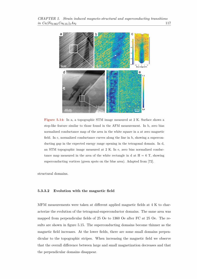
CHAPTER 5. Strain induced magneto-structural and superconducting transitionsin Ca(Fe0.965Co0.35)2As2 117
Figure 5.14: In a, a topographic STM image measured at 2 K. Surface shows a
step-like feature similar to those found in the AFM measurement. In b, zero bias
normalized conductance map of the area in the white square in a at zero magnetic
field. In c, normalized conductance curves along the line in b, showing a supercon-
ducting gap in the expected energy range opening in the tetragonal domain. In d,
an STM topographic image measured at 2 K. In e, zero bias normalized conduc-
tance map measured in the area of the white rectangle in d at H = 6 T, showing
superconducting vortices (green spots on the blue area). Adapted from [72].
structural domains.
5.3.3.2 Evolution with the magnetic field
MFM measurements were taken at different applied magnetic fields at 4 K to char-
acterize the evolution of the tetragonal-superconductor domains. The same area was
mapped from perpendicular fields of 25 Oe to 1360 Oe after FC at 25 Oe. The re-
sults are shown in figure 5.15. The superconducting domains become thinner as the
magnetic field increases. At the lower fields, there are some small domains perpen-
dicular to the topographic stripes. When increasing the magnetic field we observe
that the overall difference between large and small magnetization decreases and that
the perpendicular domains disappear.

CHAPTER 5. Strain induced magneto-structural and superconducting transitionsin Ca(Fe0.965Co0.35)2As2 118
Figure 5.15: Evolution with the applied magnetic field of the magnetic stripes.
In a, the topographic image of the area were the MFM images were measured. In
b-h the magnetic images measured at 25, 70, 300, 430, 700, 1160 and 1360 Oe
respectively. The superconducting domains (white and light yellow) become thinner
as the magnetic field increases and some small domains perpendicular to larger
domains along the vertical dimension are visible at the lower field and are not visible
at higher fields. Scale bar is 2 µm.
The AFM resolution does not allow to determine if there are smaller topographic
stripes associated to these domains. The possible origin of this orthogonal domains
will be discussed in the following section.
5.3.4 Origin of the perpendicular domains
In the previous section, it was shown that there are some superconducting domains
that are perpendicular to the topographic stripes and seems not to be related with
any feature in the topographic image. This is nicely seen in images at larger scanned
areas as the one presented in figure 5.16.
Figure 5.16 shows intersection of superconducting domains, always forming angles
of ≈ 90. This may be explained by the formation of tetragonal-orthorhombic domain
walls at each side of the twin boundaries between two orthorhombic domains as is
schematized in figure 5.16. Two orthorhombic domains in a twin boundary, form an
angle of ≈ 2 between them due to the orthorhombic distortion [69, 72]. As a result,
the angle between two tetragonal domains at both sides of a twin boundary should
differ from 90 by this small angle. This is compatible with the MFM images, where
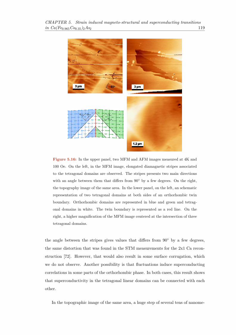
CHAPTER 5. Strain induced magneto-structural and superconducting transitionsin Ca(Fe0.965Co0.35)2As2 119
Figure 5.16: In the upper panel, two MFM and AFM images measured at 4K and
100 Oe. On the left, in the MFM image, elongated diamagnetic stripes associated
to the tetragonal domains are observed. The stripes presents two main directions
with an angle between them that differs from 90 by a few degrees. On the right,
the topography image of the same area. In the lower panel, on the left, an schematic
representation of two tetragonal domains at both sides of an orthorhombic twin
boundary. Orthorhombic domains are represented in blue and green and tetrag-
onal domains in white. The twin boundary is represented as a red line. On the
right, a higher magnification of the MFM image centered at the intersection of three
tetragonal domains.
the angle between the stripes gives values that differs from 90 by a few degrees,
the same distortion that was found in the STM measurements for the 2x1 Ca recon-
struction [72]. However, that would also result in some surface corrugation, which
we do not observe. Another possibility is that fluctuations induce superconducting
correlations in some parts of the orthorhombic phase. In both cases, this result shows
that superconductivity in the tetragonal linear domains can be connected with each
other.
In the topographic image of the same area, a huge step of several tens of nanome-
CHAPTER 5. Strain induced magneto-structural and superconducting transitionsin Ca(Fe0.965Co0.35)2As2 120
tres is shown at the centre of the image. On crossing the big step, the domain lines
perfectly match. This shows that the domain walls extend along the c axis.
5.4 Conclusions
In this chapter we have studied the effect of strain in a Ca(Fe0.965 Co0.35)2As2 single
crystal from the microscopic point of view. We have imaged the coexistence of tetrag-
onal/orthorhombic domain walls below the strains mediated transition at Ts,N (ε).
Below the superconducting critical temperature of free standing samples, we have
measured the formation of diamagnetic domains coinciding with the tetragonal do-
mains. We have associated the diamagnetic domains with the superconducting tran-
sition of the remaining tetragonal phase. We have characterized their evolution with
the applied magnetic field and the temperature. STM images are consistent with our
results, showing the opening of a superconducting gap and the existence of vortices
in the tetragonal domains below TC .
Quite likely, the size of the domains can be modified by applying uniaxial stress to
the substrate, either perpendicular or parallel to the stripes. Or simply by changing
the substrate. For instance, the thermal expansion of glass is of -0.1% which should
result in a differential thermal expansion of 0.6% between sample and substrate and
eventually lead to modified length scales in the domain size and distribution. Thus,
strain might be used as a control parameter to produce novel kinds of superconducting
systems, such as intrinsic Josephson junction arrays or to use the domain structure
to improve vortex pinning. At very low magnetic fields we observe sometimes linear
diamagnetic structures in the orthorhombic phase that might join elongated tetrago-
nal domains, suggesting that such a coupling between elongated domains can indeed
happen in some parts of the sample.
To our knowledge, this is the first experimental work showing phase separation
associated to strain below TC in pnictides. The likely absence of magnetic order
in the tetragonal domains, having in close spatial proximity a magnetically ordered
domain, suggests that magnetic and superconducting order are both antagonistic,

CHAPTER 5. Strain induced magneto-structural and superconducting transitionsin Ca(Fe0.965Co0.35)2As2 121
although they are probably fed by the same fluctuations.

CHAPTER 6
Manipulation of the crossing lattice in
Bi2Sr2CaCu2O8
6.1 Introduction
Bismuth strontium calcium copper oxide, or BSCCO, is a family of high-temperature
superconductors having the generalized chemical formula Bi2Sr2Can−1CunO2n+4,
with n = 2 being the most commonly studied compound, also called Bi-2212. Dis-
covered in 1988 [228], BSCCO was the first high-temperature superconductor which
did not contain a rare earth element. It is a cuprate superconductor, an impor-
tant category of high-temperature superconductors sharing a two-dimensional layered
(perovskite) structure with superconductivity taking place in the copper oxide planes.
The crossing lattice of Josephson vortices (JVs) and pancake vortices (PVs) in Bi-
2212 has attracted a lot of attention in the scientific community in the last decades.
Theoretical works have described the interaction between PVs and JVs at different
regimes [44, 46, 47, 49, 55] and experimentalist have imaged the crossing lattice by
several techniques like magneto optical (MO) imaging [60–62] (figure 6.1 a), Bitter
decoration [58, 59] (figure 6.1 b), and Hall microscopy [63–65] (figure 6.1 c).
Those works have characterized the crossing lattice at different polar angles and
strengths of the applied magnetic field. They have found good agreement between
123

CHAPTER 6. Manipulation of the crossing lattice in Bi2Sr2CaCu2O8 124
theory and the experimental values of the lattice parameters of the JV lattice and the
distribution of PVs on top of JVs [63, 64]. They have also achieved PVs manipulation
in some extent by using a rotating magnetic field [65]. But, the local manipulation
of single PVs and the experimental measurement of the force between PVs and JVs
has not been achieved yet. On the other hand, local manipulation of single vortices
was achieved in YBCO, another anisotropic high-TC superconductor. Authors in
[106, 113] have demonstrated that MFM can be used to manipulate vortices.
Figure 6.1: In a, a MO image measured in a Bi-2212 single crystal showing vortex
chains due to the accumulation of PVs on top of JVs. Obtained at T = 72 K, B⊥ =
13.8 Oe and B‖ = 60 Oe. In b, bitter decoration image in a Bi-2212 single crystal
showing PV chains on top of JVs with PVs in between. Obtained at T = 72 K,
B⊥ = 12 Oe and B‖ = 32 Oe. In c, a SHPM image of PV chains decorating two
JVs in a Bi-2212 single crystal at T = 81 K, B⊥ = 0.8 Oe and B‖ = 35 Oe. In the
three images, vortices appear as white dots on the black background. Adapted from
[58, 62] and [56].
6.1.1 Interaction between JVs and PVs
At small fields and high anisotropy factor, γ, PVs do not influence much the structure
of JVs. However, there is a finite interaction energy between PV stacks and JVs due
to the PVs displacements under the action of the JVs in-plane currents [46]. This
interaction causes an effective attractive force between PVs and JVs. The force per
unit length along the c-axis, between a PV stack and a JV stack was calculated in
[46] as:
fx = 1.4φ20
4π2azγ3s2log(λab/s)(6.1)

CHAPTER 6. Manipulation of the crossing lattice in Bi2Sr2CaCu2O8 125
Where φ0 is the quantum of flux, az the lattice parameter of the JV lattice in the c-
axis direction, s the distance between superconducting layers and λab the penetration
depth for superconducting currents in the a-b plane.
6.1.2 Manipulation of the crossing lattice in Bi-2212
Figure 6.2: SHPM images at T = 80 K and H‖ = 27.5 Oe, with the JV lattice
rotated by (left to right, top to bottom, anticlockwise rotation): 0, 15, 30, 45,
60, 75, 105, 120, 135, 150, 165, and 180. PVs appear as black dots in the
grey background. The black arrow indicates the direction of the magnetic field. Scan
size 28 µm × 28 µm. Adapted from [65].
Previous works have been able to manipulate the crossing lattice in Bi-2212,.
They were able to drag PVs with the JVs by changing the direction of the in-plane
magnetic field at temperatures close to TC [56, 65]. An example is presented in figure
6.2, where the crossing lattice was successfully rotated in Bi-2212 at 80 K.
Authors in [65] argue that the attraction force between JVs and PVs at 80 K
in their crystals is three times larger that the pinning force of the PVs. Therefore
changing the direction of the JVs by rotating the in-plane the magnetic field, drags

CHAPTER 6. Manipulation of the crossing lattice in Bi2Sr2CaCu2O8 126
the PVs with them.
6.1.3 Observation of crossing lattice with MFM and its manipula-
tion
6.1.3.1 Force of a MFM tip on a vortex
MFM tips exerts a given force on magnetic samples. This fact is often a disadvan-
tage, as the tip-sample interaction could change the magnetic state of the sample
and somehow introduce artefacts in the measurement [125–127, 229]. In the present
chapter, we deliberately have used this force to manipulate superconducting vortices.
We have magnetized the tip parallel to the vortices to give attraction force between
them. Such a force will decrease as the tip-sample separation increases.
To obtain an insight on the force acting on the vortices, we have followed the
calculation of the tip-vortex interaction made by [230]. This model, treats both, tip
and vortex, as monopoles. The model assumes that the tip is and infinitely long and
narrow cylinder with its mains axis and magnetization parallel to the Z axis and the
vortex as a monopole residing at a distance λ below the surface of the superconductor,
which fills the half space z<0 with a magnetic field [141, 231]:
~B(~r,z)≈ φ0(~r+ (z+λ)z)2π(R2 + (z+λ2))3/2 (6.2)
Where r is the radial distance from the tip, z the vertical distance and R the tip
radius. Thus, the force acting on the tip due to the interaction with the supercon-
ducting vortex is:
~F (~r,z)≈m~B(~r,z) (6.3)
where m is the dipolar moment per unit length of the tip. Maximizing the force of
equation 6.3 in z, we obtain:

CHAPTER 6. Manipulation of the crossing lattice in Bi2Sr2CaCu2O8 127
Fmaxz = mφ02π(z+h0)2 (6.4)
where h0 is the offset in the tip-sample separation due to the approximation of
the monopole model. The maximum lateral force is approximated as:
Fmaxlat = αFmaxz (6.5)
Here, α is a constant of proportionality with a value between 0.3 and 0.4 [231, 232].
6.1.3.2 Vortex manipulation in YBCO
Previous measurements have shown the possibility to drag vortices in the High-TCsuperconductors, YBCO [106, 113]. In particular, the authors in [106] have measured
the interaction of a moving vortex with the local disorder potential. They found an
unexpected and marked enhancement of the response of a vortex to pulling when
they wiggled it transversely. They showed that wiggling the vortex along the fast
scan direction of the MFM image, allows to move the vortex along the slow axis of
the image when the magnetic tip is close enough to the sample and therefore the
magnetic force between tip and sample increases. A schematic representation of the
process is presented in figure 6.3 together with real MFM images of stationary and
dragged vortices.
6.2 AFM/MFM studies
We have presented how previous works have manipulated individual vortices in YBCO
and groups of PVs trapped on JVs in Bi-2212 at temperatures close to TC . But,
prior to our work, individual manipulation of PVs on JV has not been studied yet.
Moreover, the force to move a PV out a JV remains unknown. This was our main
motivation and the starting point of our study in this compound.
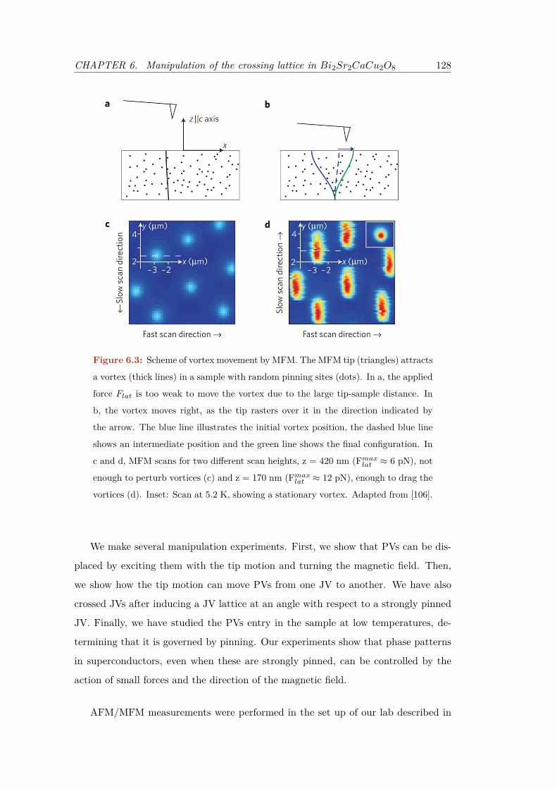
CHAPTER 6. Manipulation of the crossing lattice in Bi2Sr2CaCu2O8 128
Figure 6.3: Scheme of vortex movement by MFM. The MFM tip (triangles) attracts
a vortex (thick lines) in a sample with random pinning sites (dots). In a, the applied
force Flat is too weak to move the vortex due to the large tip-sample distance. In
b, the vortex moves right, as the tip rasters over it in the direction indicated by
the arrow. The blue line illustrates the initial vortex position, the dashed blue line
shows an intermediate position and the green line shows the final configuration. In
c and d, MFM scans for two different scan heights, z = 420 nm (Fmaxlat ≈ 6 pN), not
enough to perturb vortices (c) and z = 170 nm (Fmaxlat ≈ 12 pN), enough to drag the
vortices (d). Inset: Scan at 5.2 K, showing a stationary vortex. Adapted from [106].
We make several manipulation experiments. First, we show that PVs can be dis-
placed by exciting them with the tip motion and turning the magnetic field. Then,
we show how the tip motion can move PVs from one JV to another. We have also
crossed JVs after inducing a JV lattice at an angle with respect to a strongly pinned
JV. Finally, we have studied the PVs entry in the sample at low temperatures, de-
termining that it is governed by pinning. Our experiments show that phase patterns
in superconductors, even when these are strongly pinned, can be controlled by the
action of small forces and the direction of the magnetic field.
AFM/MFM measurements were performed in the set up of our lab described in
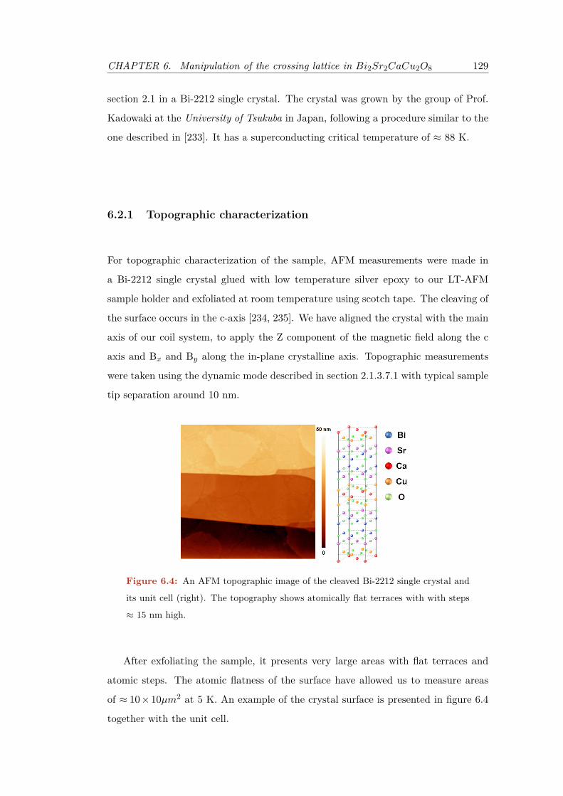
CHAPTER 6. Manipulation of the crossing lattice in Bi2Sr2CaCu2O8 129
section 2.1 in a Bi-2212 single crystal. The crystal was grown by the group of Prof.
Kadowaki at the University of Tsukuba in Japan, following a procedure similar to the
one described in [233]. It has a superconducting critical temperature of ≈ 88 K.
6.2.1 Topographic characterization
For topographic characterization of the sample, AFM measurements were made in
a Bi-2212 single crystal glued with low temperature silver epoxy to our LT-AFM
sample holder and exfoliated at room temperature using scotch tape. The cleaving of
the surface occurs in the c-axis [234, 235]. We have aligned the crystal with the main
axis of our coil system, to apply the Z component of the magnetic field along the c
axis and Bx and By along the in-plane crystalline axis. Topographic measurements
were taken using the dynamic mode described in section 2.1.3.7.1 with typical sample
tip separation around 10 nm.
Figure 6.4: An AFM topographic image of the cleaved Bi-2212 single crystal and
its unit cell (right). The topography shows atomically flat terraces with with steps
≈ 15 nm high.
After exfoliating the sample, it presents very large areas with flat terraces and
atomic steps. The atomic flatness of the surface have allowed us to measure areas
of ≈ 10×10µm2 at 5 K. An example of the crystal surface is presented in figure 6.4
together with the unit cell.

CHAPTER 6. Manipulation of the crossing lattice in Bi2Sr2CaCu2O8 130
6.2.2 Obtaining the Crossing Lattice
We have imaged the crossing lattice in our Bi-2212 single crystal using the MFMmode
described in 2.1.3.7.2. First, we have cooled the sample under an applied magnetic
field of 30 Oe in the Z direction down to 5.3 K and measured the resulting PV
distribution. We obtained the regular Abrikosov lattice with the intervortex distance
expected for the applied magnetic field (figure 6.5).
Figure 6.5: MFM image of the regular Abrikosov lattice. Measured in the Bi-2212
single crystal after FC at 5.3 K with a perpendicular magnetic field of 30 Oe.
After measuring the Abrikosov lattice, we ramped the field in Z down to zero and
applied a magnetic field of 200 Oe in the Y direction. We obtained images as shown
in Fig.6.6 a. The Abrikosov lattice is interspersed with lines of PVs pinned on JVs.
To eliminate as much as possible PVs, we heated the sample quickly above 70 K and
cooled it again to 2 K. This freed the PVs from their pinned positions and more JVs
decorated with PVs are visible (figure 6.6 b). After repeating this process several
times we have obtained areas with almost every PV pinned on top of a JV (figure 6.6
c). The same process was always used to obtain the decorated JVs in the following
sections.
Images in figure 6.6 were used to calculate the anisotropic factor of our Bi-2212
crystal (for the details of the calculation see chapter 1). Using the distance between
JVs, we have calculated γ = 250 and az = 15.4 nm. The size of the JVs was also
calculated using the relation aJV = γs/2 and bJV = s [48], finding aJV = 375nm and
bJV = 0.75nm.

CHAPTER 6. Manipulation of the crossing lattice in Bi2Sr2CaCu2O8 131
Figure 6.6: Decorated JVs with PVs. Images obtained with B‖ = 200 Oe along the
Y direction, at 5.3 K. In a, the vortex arrangement after FC with B⊥ = 30 Oe and
switching it to zero and B‖ to 200 Oe at 5.3 K. Some decorated JVs are visible with
a significant number of trapped PVs in between. In b, a different configuration after
heating the sample up to 70 K and cooling it down again to 5.3 K. More decorated
JVs are visible and the number of PVs in between have decreased. After repeating
the same process several times, almost all the PVs are decorating JVs (c). The
field of view has moved during heating, so the images are not taken at the same
position. In d, a schematic representation of the JV lattice in Bi-2212. The gray
lines represent the CuO planes and the red ellipses the JVs.
The penetration depth, λab, of Bi-2212 single crystals was experimentally deter-
mined in previous works using different methods [143–145, 236]. These works have
reported values between 180-270 nm for λab. Thus, the lateral size of the PVs and
the JVs is comparable. Therefore, only one PV row fits inside a JV.
6.2.3 Evolution of the crossing lattice with the temperature
We have measured the evolution of the crossing lattice at the same area for differ-
ent temperatures. Images in figure 6.7 were measured at 5.5 K, 12 K and 15.5 K.
They show that the vortices width increases with the temperature. At 20 K the flux
distribution becomes homogeneous over the surface and no magnetic contrast was
obtained. This, suggest that PVs are able to move far enough from their equilib-
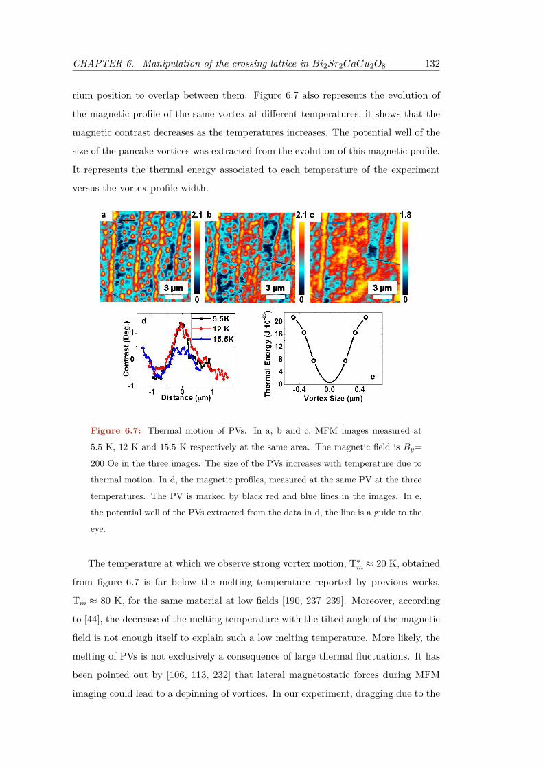
CHAPTER 6. Manipulation of the crossing lattice in Bi2Sr2CaCu2O8 132
rium position to overlap between them. Figure 6.7 also represents the evolution of
the magnetic profile of the same vortex at different temperatures, it shows that the
magnetic contrast decreases as the temperatures increases. The potential well of the
size of the pancake vortices was extracted from the evolution of this magnetic profile.
It represents the thermal energy associated to each temperature of the experiment
versus the vortex profile width.
Figure 6.7: Thermal motion of PVs. In a, b and c, MFM images measured at
5.5 K, 12 K and 15.5 K respectively at the same area. The magnetic field is By=
200 Oe in the three images. The size of the PVs increases with temperature due to
thermal motion. In d, the magnetic profiles, measured at the same PV at the three
temperatures. The PV is marked by black red and blue lines in the images. In e,
the potential well of the PVs extracted from the data in d, the line is a guide to the
eye.
The temperature at which we observe strong vortex motion, T∗m ≈ 20 K, obtained
from figure 6.7 is far below the melting temperature reported by previous works,
Tm ≈ 80 K, for the same material at low fields [190, 237–239]. Moreover, according
to [44], the decrease of the melting temperature with the tilted angle of the magnetic
field is not enough itself to explain such a low melting temperature. More likely, the
melting of PVs is not exclusively a consequence of large thermal fluctuations. It has
been pointed out by [106, 113, 232] that lateral magnetostatic forces during MFM
imaging could lead to a depinning of vortices. In our experiment, dragging due to the
CHAPTER 6. Manipulation of the crossing lattice in Bi2Sr2CaCu2O8 133
magnetostatic attraction between PVs and tip could also play a significant role, which
suggest that the vortex-probe interaction is large enough to force PVs to move outside
their equilibrium position at temperatures above 20K. This result gives a powerful
tool to vortex manipulation in this system, as it shows that PVs can be manipulated
by the MFM probe at reasonable low temperatures.
6.2.4 Manipulation of the crossing lattice
We have successfully manipulated the crossing lattice in our crystal. As a first step,
we have manipulated a disordered arrangement of PVs. Then, we have successfully
manipulated PV rows pinned on JVs.
6.2.4.1 Manipulation of PVs
We have successfully manipulated PVs combining the action of the in-plane magnetic
field and the force of the MFM tip on the PVs. Figure 6.8 shows the evolution of
an arbitrary arrangement of PVs when changing the angle of the in-plane magnetic
field. The fast scan axis of the MFM is parallel to the X direction in all images.
Figure 6.8 a, shows the original configuration of PVs, with round shapes and well
localized positions at 12 K. After rotating the magnetic field by 10 degrees (figure
6.8 b) the same area was measured again. In the image, several PV magnetic profiles
are elongated in the direction of the magnetic field. This behaviour is better seen
after changing the angle to 45 (figure 6.8 c), 70 (figure 6.8 d) and 90 (figure 6.8
e). PV profiles became more elongated as the angle between the slow scan axis and
the in-plane magnetic field decreases, always following the direction of the magnetic
field. The elongation is maximum when the magnetic field is aligned with the slow
axis of the MFM. Figure 6.8 f, summarizes the evolution of the PV elongation as a
function of the angle between the fast scan axis and the magnetic field.
As discussed in the previous paragraph, we can ascribe such elongated magnetic
patterns to vortices moving below the tip. The stray field of the MFM tip exerts
a given lateral force, Flat, on the vortices. The lateral force can be decomposed in

CHAPTER 6. Manipulation of the crossing lattice in Bi2Sr2CaCu2O8 134
two components, Flat,s and Flat,f in the directions of the slow and fast scan axis
respectively. Flat,f shakes the vortices, moving them back and forth on its potential
well while Flat,s can be use to drag vortices along the scan axis if the gain in energy
of the vortex due to Flat,f is enough [106, 109, 230] (figure 6.9 a). Such a scenario is
of course not compatible with a perfect harmonic potential at a single pinning site.
Instead, it suggests that vortices have multiple relaxation time scales. They seem to
remain at positions far from equilibrium for a long time. Between each passage of
the tip there are a few ms. This seems to be compatible with the complex pinning
patterns and vortex trajectories observed in recent SOT measurements [240].
Figure 6.8: Motion of PVs by the combined action of the MFM tip and the rotating
magnetic field. We show the evolution of a set of PVs when changing the direction
of B‖ = 200 Oe (marked as a yellow arrow in the images). In a, b, c, d and e, MFM
images measured with an angle of B‖ with respect the X axis of 0, 10, 45, 70
and 90 respectively. Some PVs presents elongated magnetic profiles in the direction
of B‖ as the angle increases. The direction of the fast scan axis is represented by
a yellow arrow at the bottom. In f, we show the average PVs displacement vs the
angle, the line is a guide to the eye.
In addition, a parallel magnetic field applied to Bi-2112, will enter the material
in form of JVs. As a consequence, superconducting currents flow on the CuO planes
perpendicular to the direction of B‖. These currents exerts a Lorentz force, FL, on
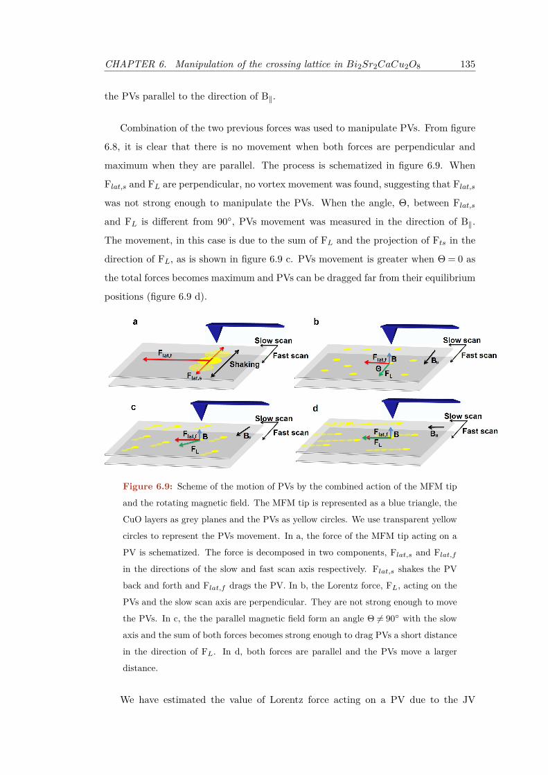
CHAPTER 6. Manipulation of the crossing lattice in Bi2Sr2CaCu2O8 135
the PVs parallel to the direction of B‖.
Combination of the two previous forces was used to manipulate PVs. From figure
6.8, it is clear that there is no movement when both forces are perpendicular and
maximum when they are parallel. The process is schematized in figure 6.9. When
Flat,s and FL are perpendicular, no vortex movement was found, suggesting that Flat,swas not strong enough to manipulate the PVs. When the angle, Θ, between Flat,sand FL is different from 90, PVs movement was measured in the direction of B‖.
The movement, in this case is due to the sum of FL and the projection of Fts in the
direction of FL, as is shown in figure 6.9 c. PVs movement is greater when Θ = 0 as
the total forces becomes maximum and PVs can be dragged far from their equilibrium
positions (figure 6.9 d).
Figure 6.9: Scheme of the motion of PVs by the combined action of the MFM tip
and the rotating magnetic field. The MFM tip is represented as a blue triangle, the
CuO layers as grey planes and the PVs as yellow circles. We use transparent yellow
circles to represent the PVs movement. In a, the force of the MFM tip acting on a
PV is schematized. The force is decomposed in two components, Flat,s and Flat,fin the directions of the slow and fast scan axis respectively. Flat,s shakes the PV
back and forth and Flat,f drags the PV. In b, the Lorentz force, FL, acting on the
PVs and the slow scan axis are perpendicular. They are not strong enough to move
the PVs. In c, the the parallel magnetic field form an angle Θ 6= 90 with the slow
axis and the sum of both forces becomes strong enough to drag PVs a short distance
in the direction of FL. In d, both forces are parallel and the PVs move a larger
distance.
We have estimated the value of Lorentz force acting on a PV due to the JV
CHAPTER 6. Manipulation of the crossing lattice in Bi2Sr2CaCu2O8 136
supercurrents. We have used the expression for the supercurrents flowing on the
surface due to the presence of JVs from [48]:
J‖ ≈φ0
µ02πλ⊥λ2‖
(6.6)
From equation 6.6 we have estimated the force acting on a PVs of about 50 pN.
Pinning force of PVs is therefore stronger as FL by itself is not enough to drag PVs. We
have calculated the force exerted by the MFM probe on a PV by using the equation
6.5. For our calculation we have use typical values of α = 0.35, h0 = 250 nm and
m= 30 nAm following [122, 230, 241], and the experimental tip-sample separation of
120 nm, obtaining Fmaxlat = 80pN. PVs movement was achieved by the combination of
the force of the MFM tip and the Lorentz force. Thus, we estimate the force needed
to drag isolated PVs of ≈ 130 pN.
6.2.4.2 Manipulation of PVs on top of JVs
Figure 6.10 a, shows JVs decorated with PVs at 5.3 K. In the image, the in plane
component of the magnetic field is aligned with the slow axis of the scan. PVs are
well localized on top of the JVs with some clusters in between, without any signature
of vortex movement. After changing the direction of the scan by 90 and increasing
the temperature up to 12 K, the same area was measured again. Result are presented
in figures 6.10 b and c.
Figure 6.10 b, was obtained by scanning from the bottom to the top and from
right to left of the image while 6.10 c, was obtained by scanning from the top to
the bottom and from right to left. From visual inspection is clear that the straight
trajectories of the PVs follow the direction of the tip during the scan.
In this case PVs are not randomly arranged on the surface but pinned on JVs
forming rows. In this particular configuration we have found PVs movement in the
direction of the scan. In this case, the force on the PVs from the tip is strong enough
to depin them from the JVs, moving them from one JV to another. The process is
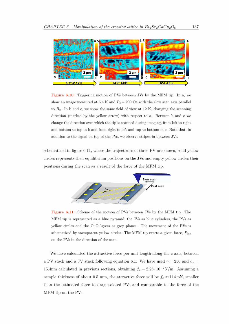
CHAPTER 6. Manipulation of the crossing lattice in Bi2Sr2CaCu2O8 137
Figure 6.10: Triggering motion of PVs between JVs by the MFM tip. In a, we
show an image measured at 5.4 K and Bx= 200 Oe with the slow scan axis parallel
to Bx. In b and c, we show the same field of view at 12 K, changing the scanning
direction (marked by the yellow arrow) with respect to a. Between b and c we
change the direction over which the tip is scanned during imaging, from left to right
and bottom to top in b and from right to left and top to bottom in c. Note that, in
addition to the signal on top of the JVs, we observe stripes in between JVs.
schematized in figure 6.11, where the trajectories of three PV are shown, solid yellow
circles represents their equilibrium positions on the JVs and empty yellow circles their
positions during the scan as a result of the force of the MFM tip.
Figure 6.11: Scheme of the motion of PVs between JVs by the MFM tip. The
MFM tip is represented as a blue pyramid, the JVs as blue cylinders, the PVs as
yellow circles and the CuO layers as grey planes. The movement of the PVs is
schematized by transparent yellow circles. The MFM tip exerts a given force, Flaton the PVs in the direction of the scan.
We have calculated the attractive force per unit length along the c-axis, between
a PV stack and a JV stack following equation 6.1. We have used γ = 250 and az =
15.4nm calculated in previous sections, obtaining fx = 2.28 · 10−7N/m. Assuming a
sample thickness of about 0.5 mm, the attractive force will be fx ≈ 114 pN, smaller
than the estimated force to drag isolated PVs and comparable to the force of the
MFM tip on the PVs.

CHAPTER 6. Manipulation of the crossing lattice in Bi2Sr2CaCu2O8 138
6.2.5 Manipulation with the aim to cross Josephson vortices
Previous works have demonstrated that the JV-PV interaction is sufficiently strong
to indirectly pin JVs stacks at the location of pinned PVs [242]. We have used this
behaviour to generate and keep a JV in a fixed direction and then cross other JVs
with it by rotating the in-plane magnetic field.
Figure 6.12: Crossing JVs. In a, a JV (denoted by JV1) pinned at a topographic
feature at 5.3 K and B‖ = 200 Oe. In b, the same area, measure after heat the
sample up to 20 K and modifing the direction of B‖ by -5 with respect to the Y
axis. Three new JVs appear in the image, two of them (denoted as JV2 and JV3)
cross JV1. In c, after heat and cool the sample again, JV2 and JV3 have changed
slightly their position. We mark the previous position of JV1 and JV2 by dashed
yellow lines. Remarkably, JV2 is attracted to JV1 and JV3 intersects JV1.
After finding an area with a longitudinal topographic feature, we have applied a
tilted magnetic field with B‖, parallel to the topographic feature, generating a series
of decorated JVs at 5.3K. As a result, one JV and several PVs were pinned to the
topographic feature. Then, we have heated the sample up to 20 K and cooled down to
5.3 K quickly. After that, we have measured the same area again. All PVs that were
pinned on the JVs where depinned, except the ones on the JV on the topographic
feature labelled as JV1 (figure 6.12 a). The pancake intervortex distances within the
feature are consistent with the presence of a JV, indicating that the original JV is still
pinned to the feature. Then, the angle of the in-plane magnetic field was changed by
-5 generating a new JV lattice tilted 5 with respect to the topographic feature. The
new JV lattice crosses the topographic feature in two points (figure 6.12 b). Finally,
the sample was heated up to 20 K and cooled down again to 5.5K to favour the JV
lattice movement. After scanning the area again, we have found that the JVs have
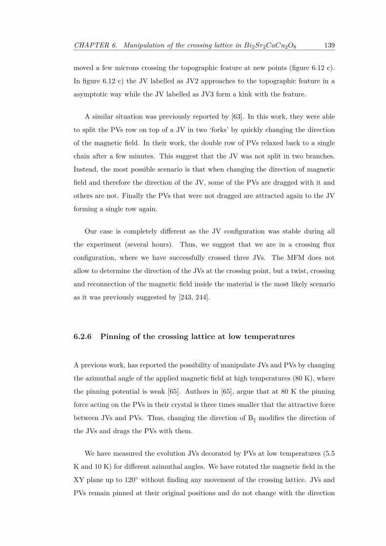
CHAPTER 6. Manipulation of the crossing lattice in Bi2Sr2CaCu2O8 139
moved a few microns crossing the topographic feature at new points (figure 6.12 c).
In figure 6.12 c) the JV labelled as JV2 approaches to the topographic feature in a
asymptotic way while the JV labelled as JV3 form a kink with the feature.
A similar situation was previously reported by [63]. In this work, they were able
to split the PVs row on top of a JV in two ‘forks’ by quickly changing the direction
of the magnetic field. In their work, the double row of PVs relaxed back to a single
chain after a few minutes. This suggest that the JV was not split in two branches.
Instead, the most possible scenario is that when changing the direction of magnetic
field and therefore the direction of the JV, some of the PVs are dragged with it and
others are not. Finally the PVs that were not dragged are attracted again to the JV
forming a single row again.
Our case is completely different as the JV configuration was stable during all
the experiment (several hours). Thus, we suggest that we are in a crossing flux
configuration, where we have successfully crossed three JVs. The MFM does not
allow to determine the direction of the JVs at the crossing point, but a twist, crossing
and reconnection of the magnetic field inside the material is the most likely scenario
as it was previously suggested by [243, 244].
6.2.6 Pinning of the crossing lattice at low temperatures
A previous work, has reported the possibility of manipulate JVs and PVs by changing
the azimuthal angle of the applied magnetic field at high temperatures (80 K), where
the pinning potential is weak [65]. Authors in [65], argue that at 80 K the pinning
force acting on the PVs in their crystal is three times smaller that the attractive force
between JVs and PVs. Thus, changing the direction of B‖ modifies the direction of
the JVs and drags the PVs with them.
We have measured the evolution JVs decorated by PVs at low temperatures (5.5
K and 10 K) for different azimuthal angles. We have rotated the magnetic field in the
XY plane up to 120 without finding any movement of the crossing lattice. JVs and
PVs remain pinned at their original positions and do not change with the direction
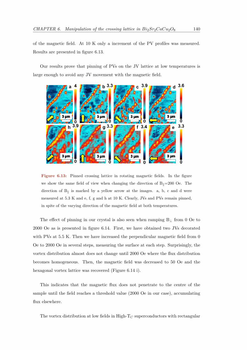
CHAPTER 6. Manipulation of the crossing lattice in Bi2Sr2CaCu2O8 140
of the magnetic field. At 10 K only a increment of the PV profiles was measured.
Results are presented in figure 6.13.
Our results prove that pinning of PVs on the JV lattice at low temperatures is
large enough to avoid any JV movement with the magnetic field.
Figure 6.13: Pinned crossing lattice in rotating magnetic fields. In the figure
we show the same field of view when changing the direction of B‖=200 Oe. The
direction of B‖ is marked by a yellow arrow at the images. a, b, c and d were
measured at 5.3 K and e, f, g and h at 10 K. Clearly, JVs and PVs remain pinned,
in spite of the varying direction of the magnetic field at both temperatures.
The effect of pinning in our crystal is also seen when ramping B⊥ from 0 Oe to
2000 Oe as is presented in figure 6.14. First, we have obtained two JVs decorated
with PVs at 5.5 K. Then we have increased the perpendicular magnetic field from 0
Oe to 2000 Oe in several steps, measuring the surface at each step. Surprisingly, the
vortex distribution almost does not change until 2000 Oe where the flux distribution
becomes homogeneous. Then, the magnetic field was decreased to 50 Oe and the
hexagonal vortex lattice was recovered (Figure 6.14 i).
This indicates that the magnetic flux does not penetrate to the centre of the
sample until the field reaches a threshold value (2000 Oe in our case), accumulating
flux elsewhere.
The vortex distribution at low fields in High-TC superconductors with rectangular
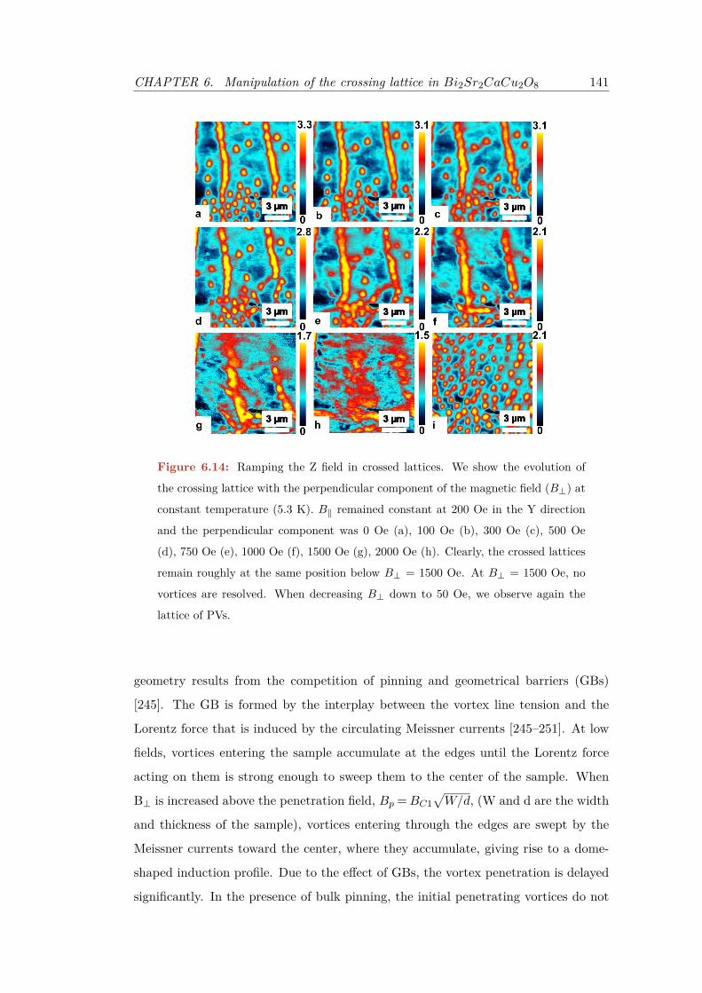
CHAPTER 6. Manipulation of the crossing lattice in Bi2Sr2CaCu2O8 141
Figure 6.14: Ramping the Z field in crossed lattices. We show the evolution of
the crossing lattice with the perpendicular component of the magnetic field (B⊥) at
constant temperature (5.3 K). B‖ remained constant at 200 Oe in the Y direction
and the perpendicular component was 0 Oe (a), 100 Oe (b), 300 Oe (c), 500 Oe
(d), 750 Oe (e), 1000 Oe (f), 1500 Oe (g), 2000 Oe (h). Clearly, the crossed lattices
remain roughly at the same position below B⊥ = 1500 Oe. At B⊥ = 1500 Oe, no
vortices are resolved. When decreasing B⊥ down to 50 Oe, we observe again the
lattice of PVs.
geometry results from the competition of pinning and geometrical barriers (GBs)
[245]. The GB is formed by the interplay between the vortex line tension and the
Lorentz force that is induced by the circulating Meissner currents [245–251]. At low
fields, vortices entering the sample accumulate at the edges until the Lorentz force
acting on them is strong enough to sweep them to the center of the sample. When
B⊥ is increased above the penetration field, Bp =BC1√W/d, (W and d are the width
and thickness of the sample), vortices entering through the edges are swept by the
Meissner currents toward the center, where they accumulate, giving rise to a dome-
shaped induction profile. Due to the effect of GBs, the vortex penetration is delayed
significantly. In the presence of bulk pinning, the initial penetrating vortices do not
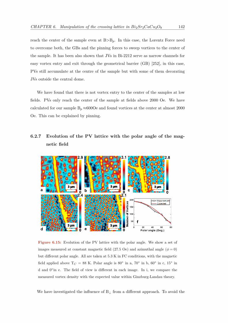
CHAPTER 6. Manipulation of the crossing lattice in Bi2Sr2CaCu2O8 142
reach the center of the sample even at B>Bp. In this case, the Lorentz Force need
to overcome both, the GBs and the pinning forces to sweep vortices to the center of
the sample. It has been also shown that JVs in Bi-2212 serve as narrow channels for
easy vortex entry and exit through the geometrical barrier (GB) [252], in this case,
PVs still accumulate at the centre of the sample but with some of them decorating
JVs outside the central dome.
We have found that there is not vortex entry to the center of the samples at low
fields. PVs only reach the center of the sample at fields above 2000 Oe. We have
calculated for our sample Bp ≈600Oe and found vortices at the center at almost 2000
Oe. This can be explained by pinning.
6.2.7 Evolution of the PV lattice with the polar angle of the mag-
netic field
Figure 6.15: Evolution of the PV lattice with the polar angle. We show a set of
images measured at constant magnetic field (27.5 Oe) and azimuthal angle (φ= 0)
but different polar angle. All are taken at 5.3 K in FC conditions, with the magnetic
field applied above TC = 88 K. Polar angle is 80 in a, 70 in b, 60 in c, 15 in
d and 0in e. The field of view is different in each image. In i, we compare the
measured vortex density with the expected value within Ginzburg-Landau theory.
We have investigated the influence of B⊥ from a different approach. To avoid the

CHAPTER 6. Manipulation of the crossing lattice in Bi2Sr2CaCu2O8 143
pinning of the PVs, each measurement was taken at FC conditions. The sample was
heated above its critical temperature and the absolute value of the magnetic field
was held constant to 27.5 Oe for different polar angles. Then, the sample was cooled
down to 5.5 K. This procedure avoids the effect of pinning and allows to measure the
evolution of the lattice at different angles, but does not allow to measure an specific
area due to the thermal drift of the sample. Results are summarized in Figure 6.15.
All images of 12× 12µm2 were measured at different positions of a larger area
about 30×30µm2. The number of vortices at the area, follows the expected behaviour
(figure 6.15 g), indicating that at high temperatures where the pinning potential is
smaller, PVs enter to the centre of the sample with an homogeneous distribution.
6.3 Conclusions
In this chapter, we have studied the crossing lattice of Bi-2212 single crystal at low
temperatures and low fields. We have successfully manipulated an arbitrary arrange-
ment of PVs and the crossing lattice of JVs and PVs. We have measured the depen-
dence of the PV movement with the angle between the in-plane magnetic field and
the scan of the MFM. We have measured the necessary force to manipulate isolated
PVs and PVs trapped on JVs, finding values of ≈ 120pN . We were able to cross three
JVs. We have also demonstrated that pinning determines the entry of PVs from the
edges to the centre of the sample at low temperatures.
To our knowledge,this is the first work showing local manipulation of the crossing
lattice in a superconductor.

CHAPTER 7
General conclusions
In this project we have used magnetic force microscopy at low temperatures to study
three different superconducting compounds. We have focused our research in the
study of superconducting vortices and their manipulation. We have also studied
the decomposition in superconducting and ferromagnetic domains in a Ca(Fe0.965
Co0.035)2As2 single crystal and the exfoliation and deposition of several 2D systems.
Regarding the experimental system, we have used a set-up that allows us to perform
AFM-MFM measurements between 1.8 K and 300 K, applying magnetic fields in any
direction of the space up to 5 T in the Z direction and 1.2 T in the X and Y directions.
With this set up, we have characterized for the first time the hysteresis cycle of
MFM commercial probes as a function of the temperature from 1.8 to 300 K. We have
also found that the MFM images of superconducting vortices show star-like features
at vortex positions when the MFM tip is magnetized bellow its coercive field.
We have successfully exfoliated several superconducting crystals and graphene and
deposit them in different substrates using a combination of PDMS silicon stamps and
the regular scotch tape method. We have investigated three different systems with
this method, BSCCO on SiO2, β-Bi2Pd on SiO2 and graphene and FLG on β-Bi2Pd.
In the case of BSCCO flakes deposited in SiO2, we were able to measure one thick
flake at low temperatures and characterize its magnetic profile in the superconducting
state at different magnetic fields and temperatures.
145
CHAPTER 7. General conclusions 146
For β-Bi2Pd flakes deposited on SiO2, we were able to exfoliate and deposit flakes
of this system for the very first time, down to some tens of nanometers. This results
open the possibility to study the superconducting behavior in the 2D limit in this
system in the future.
We have also transfered graphene and FLG flakes on top of a β-Bi2Pd single crystal
and developed a experimental procedure to unambiguously localize graphene and FLG
flakes on top of β-Bi2Pd using a combination of friction and KPM measurements with
an AFM. We have also probed that this method allow to localize the flakes at ambient
and at low humidity conditions.
We have observed two different regimes in the patterns of pinned superconduct-
ing vortices at low magnetic fields in the single gap superconductor β-Bi2Pd. We
have shown that lines of vortices form at defects due to pinning at very low magnetic
fields, while at higher fields the vortex lattice acts as a whole, leaving a regular hexag-
onal lattice even below Hc1. Crystalline strain close to defects determines the vortex
arrangements at low fields and leads to sizable modifications of the local supercon-
ducting screening properties, as shown by the measured increase in the penetration
depth λ close to defects.
We have transfered a ≈ 1 cm × 1 cm graphene sheet on top of a β-Bi2Pd single
crystal with the electromechanical transfer method and measured the vortex lattice
of the β-Bi2Pd crystal at the superconducting state at 2K trough the graphene layer.
This experiment, opens the possibility of characterize this heterostructure in future
experiments to determine if there is a gap opening in the graphene in this situation.
We have studied the effect of strain in a Ca(Fe0.965 Co0.35)2As2 single crystal
from the microscopic point of view. We have imaged the coexistence of tetrago-
nal/orthorhombic domain walls bellow the strains mediated transition at Ts,N (ε).
Bellow the superconducting critical temperature of free standing samples, we have
measured the formation of diamagnetic domains coinciding with the tetragonal do-
mains. We have associated the diamagnetic domains with the superconducting transi-
tion of the remaining tetragonal phase. We have characterized their evolution with the
applied magnetic field and the temperature. At very low magnetic fields we observe

CHAPTER 7. General conclusions 147
linear diamagnetic structures in the orthorhombic phase that might join elongated
tetragonal domains, suggesting that such a coupling between elongated domains can
indeed happen in some parts of the sample. To our knowledge, ours is the first exper-
imental work showing phase separation associated to strain bellow TC in pnictides.
We have studied the crossing lattice in a Bi-2212 single crystal at low temperatures
and low fields. We have successfully manipulated an arbitrary arrangement of PVs
and the crossing lattice of JVs and PVs. We have measured the dependence of the
PV movement with the angle between the in-plane magnetic field and the scan of the
MFM. We have measured the necessary force to manipulate isolated PVs and PVs
trapped on JVs. We were able to cross three JVs. To our knowledge, ours is the first
work showing manipulation of the crossing lattice in a superconductor.
In summary, we have addressed systems that include proximity induced supercon-
ductivity in graphene, phase separation induced by coexistence with magnetic order
and observation and manipulation of 2D vortex lattices. We have found new results,
as the increase in penetration depth in graphene when decreasing the coupling with
a superconductor, we have shown the existence of a new intrinsically inhomogeneous
superconductor and have characterized complex phase patterns in a 2D supercon-
ductor. The combination of AFM and MFM in a vector magnet provides a useful
platform to study and manipulate novel forms of superconductivity.


Bibliography
[1] Gianni Profeta, Matteo Calandra, and Francesco Mauri. Phonon-mediated
superconductivity in graphene by lithium deposition. Nat Phys, 8(2):131–134,
Feb 2012.
[2] A. Di Bernardo, O. Millo, M. Barbone, H. Alpern, Y. Kalcheim, U. Sassi, A. K.
Ott, D. De Fazio, D. Yoon, M. Amado, A. C. Ferrari, J. Linder, and J. W. A.
Robinson. p-wave triggered superconductivity in single-layer graphene on an
electron-doped oxide superconductor. 8:14024 EP –, Jan 2017. Article.
[3] Rekha Narayan and Sang Ouk Kim. Surfactant mediated liquid phase exfolia-
tion of graphene. Nano Converg, 2(1):20, Oct 2015. 50[PII].
[4] Sajedeh Manzeli, Dmitry Ovchinnikov, Diego Pasquier, Oleg V. Yazyev, and
Andras Kis. 2d transition metal dichalcogenides. 2:17033 EP –, Jun 2017.
Review Article.
[5] Rui Dong and Irma Kuljanishvili. Review article: Progress in fabrication of
transition metal dichalcogenides heterostructure systems. Journal of Vacuum
Science & Technology B, Nanotechnology and Microelectronics: Materials, Pro-
cessing, Measurement, and Phenomena, 35(3):030803, 2017.
[6] Miguel Ayan-Varela, Oscar Perez-Vidal, Juan I. Paredes, Jose M. Munuera,
Silvia Villar-Rodil, Maria Diaz-Gonzalez, Cesar Fernandez-Sanchez, Virgilia S.
Silva, MÃşnica Cicuendez, Mercedes Vila, Amelia Martinez-Alonso, and Juan
M. D. Tascon. Aqueous exfoliation of transition metal dichalcogenides assisted
by dna/rna nucleotides: Catalytically active and biocompatible nanosheets
stabilized by acid-base interactions. ACS Applied Materials & Interfaces,
9(3):2835–2845, 2017. PMID: 28029778.
149
Bibliography 150
[7] Christophe Brun, Tristan Cren, and Dimitri Roditchev. Review of 2d supercon-
ductivity: the ultimate case of epitaxial monolayers. Superconductor Science
and Technology, 30(1):013003, 2017.
[8] Takashi Uchihashi. Two-dimensional superconductors with atomic-scale thick-
ness. Superconductor Science and Technology, 30(1):013002, 2017.
[9] A T Bollinger and I Bozovic. Two-dimensional superconductivity in the cuprates
revealed by atomic-layer-by-layer molecular beam epitaxy. Superconductor Sci-
ence and Technology, 29(10):103001, 2016.
[10] X. Wang, L. X. You, D. K. Liu, C. T. Lin, X. M. Xie, and M. H. Jiang. Thin-
film-like BSCCO single crystals made by mechanical exfoliation. pages 13–17,
2012.
[11] Yuan Huang, Eli Sutter, Norman N. Shi, Jiabao Zheng, Tianzhong Yang, Dirk
Englund, Hong-Jun Gao, and Peter Sutter. Reliable exfoliation of large-area
high-quality flakes of graphene and other two-dimensional materials. ACS Nano,
9(11):10612–10620, 2015. PMID: 26336975.
[12] Efrén Navarro-Moratalla, Joshua O. Island, Samuel Mañas-Valero, Elena
Pinilla-Cienfuegos, Andres Castellanos-Gomez, Jorge Quereda, Gabino Rubio-
Bollinger, Luca Chirolli, Jose Angel Silva-Guillén, Nicolás Agraït, Gary A.
Steele, Francisco Guinea, Herre S. J. van der Zant, and Eugenio Coronado.
Enhanced superconductivity in atomically thin TaS2. 7:11043 EP –, Mar 2016.
Article.
[13] Katsuyoshi Komatsu, Chuan Li, S. Autier-Laurent, H. Bouchiat, and
S. Guéron. Superconducting proximity effect in long superconduc-
tor/graphene/superconductor junctions: From specular andreev reflection at
zero field to the quantum hall regime. Phys. Rev. B, 86:115412, Sep 2012.
[14] C. Ojeda-Aristizabal, M. Ferrier, S. Guéron, and H. Bouchiat. Tuning the
proximity effect in a superconductor-graphene-superconductor junction. Phys.
Rev. B, 79:165436, Apr 2009.
[15] M Hayashi, H Yoshioka, and A Kanda. Superconducting proximity ef-
Bibliography 151
fect in graphene nanostructures. Journal of Physics: Conference Series,
248(1):012002, 2010.
[16] Chuan Li. Superconducting proximity effect in graphene and Bi nanowire based
junctions. PhD thesis, Universite Paris, 2014.
[17] Jungdae Kim, Victor Chua, Gregory A. Fiete, Hyoungdo Nam, Allan H. Mac-
Donald, and Chih-Kang Shih. Visualization of geometric influences on proxim-
ity effects in heterogeneous superconductor thin films. Nat Phys, 8(6):464–469,
Jun 2012. Letter.
[18] Jun-Yi Ge, Joffre Gutierrez, A. Lyashchenko, V. Filipov, Jun Li, and Victor V.
Moshchalkov. Direct visualization of vortex pattern transition in ZrB12 with
ginzburg-landau parameter close to the dual point. Phys. Rev. B, 90:184511,
Nov 2014.
[19] Victor Moshchalkov, Mariela Menghini, T. Nishio, Q. H. Chen, A. V. Silhanek,
V. H. Dao, L. F. Chibotaru, N. D. Zhigadlo, and J. Karpinski. Type-1.5 super-
conductivity. Phys. Rev. Lett., 102:117001, Mar 2009.
[20] J. Gutierrez, B. Raes, A. V. Silhanek, L. J. Li, N. D. Zhigadlo, J. Karpinski,
J. Tempere, and V. V. Moshchalkov. Scanning hall probe microscopy of uncon-
ventional vortex patterns in the two-gap MgB2 superconductor. Phys. Rev. B,
85:094511, Mar 2012.
[21] Taichiro Nishio, Vu Hung Dao, Qinghua Chen, Liviu F. Chibotaru, Kazuo
Kadowaki, and Victor V. Moshchalkov. Scanning squid microscopy of vortex
clusters in multiband superconductors. Phys. Rev. B, 81:020506, Jan 2010.
[22] H. J. Zhao, V. R. Misko, J. Tempere, and F. Nori. Pattern formation in vortex
matter with pinning and frustrated intervortex interactions. Phys. Rev. B,
95:104519, Mar 2017.
[23] E. Herrera, I. Guillamón, J. A. Galvis, A. Correa, A. Fente, R. F. Luccas, F. J.
Mompean, M. García-Hernández, S. Vieira, J. P. Brison, and H. Suderow. Mag-
netic field dependence of the density of states in the multiband superconductor
β−bi2Pd. Phys. Rev. B, 92:054507, Aug 2015.

Bibliography 152
[24] E. et al Herrera. Preprint. 2016.
[25] J. Kačmarčík, Z. Pribulová, T. Samuely, P. Szabó, V. Cambel, J. Šoltýs, E. Her-
rera, H. Suderow, A. Correa-Orellana, D. Prabhakaran, and P. Samuely. Single-
gap superconductivity in β−Bi2Pd. Phys. Rev. B, 93:144502, Apr 2016.
[26] H. Kamelingh Onnes. Leiden Commum., 120B:122, 1911.
[27] W. Meissner and R. Ochsenfeld. Ein neuer effekt bei eintritt der supraleit-
fähigkeit. Naturwissenschaften, 21(44):787–788, 1933.
[28] Michael Tinkham. Introduction to Superconductivity. McGRAW-HILL, 1974.
[29] Charles Poole Horacio Farach Richard Creswick Ruslan Prozorov. Supercon-
ductivity. Elsevier, 2014.
[30] F. London and H. London. The electromagnetic equations of the supraconduc-
tor. Proceedings of the Royal Society of London A: Mathematical, Physical and
Engineering Sciences, 149(866):71–88, 1935.
[31] L.D. Landau V.L. Ginzburg. Zh.Eksp.Teor.Fiz, 20:1064–1082, 1950.
[32] J. Bardeen, L. N. Cooper, and J. R. Schrieffer. Microscopic theory of supercon-
ductivity. Phys. Rev., 106:162–164, Apr 1957.
[33] A. A. Abrikosov. Zh. Eksp. i Teor. Fiz., 32B:1442, 1957.
[34] Leon N. Cooper. Bound electron pairs in a degenerate fermi gas. Phys. Rev.,
104:1189–1190, Nov 1956.
[35] H. Fröhlich. Theory of the superconducting state. i. the ground state at the
absolute zero of temperature. Phys. Rev., 79:845–856, Sep 1950.
[36] T. E. Faber. The Intermediate State in Superconducting Plates. Proceedings of
the Royal Society of London Series A, 248:460–481, December 1958.
[37] E. H. Brandt and U. Essmann. phys. stat. sol.(b), 13:144, 1987.
[38] D. R. Aston, L. W. Dubeck, and F. Rothwarf. "intermediate mixed" state of
type-ii superconductors. Phys. Rev. B, 3:2231–2236, Apr 1971.
Bibliography 153
[39] S. Mühlbauer, C. Pfleiderer, P. Böni, M. Laver, E. M. Forgan, D. Fort, U. Kei-
derling, and G. Behr. Morphology of the superconducting vortex lattice in
ultrapure niobium. Phys. Rev. Lett., 102:136408, Apr 2009.
[40] Ernst Helmut Brandt and Mukunda P. Das. Attractive vortex interaction and
the intermediate-mixed state of superconductors. Journal of Superconductivity
and Novel Magnetism, 24(1):57–67, Jan 2011.
[41] Jeudy, V. and Gourdon, C. Instability-driven formation of domains in the
intermediate state of type-i superconductors. Europhys. Lett., 75(3):482–488,
2006.
[42] John R. Clem. Two-dimensional vortices in a stack of thin superconducting
films: A model for high-temperature superconducting multilayers. Phys. Rev.
B, 43:7837–7846, Apr 1991.
[43] S. E. Savel’ev, J. Mirković, and K. Kadowaki. London theory of the crossing
vortex lattice in highly anisotropic layered superconductors. Phys. Rev. B,
64:094521, Aug 2001.
[44] A. E. Koshelev. Crossing lattices, vortex chains, and angular dependence of
melting line in layered superconductors. Phys. Rev. Lett., 83:187–190, Jul 1999.
[45] John R. Clem. Pancake vortices. Journal of Superconductivity, 17(5):613–629,
Oct 2004.
[46] A. E. Koshelev. Josephson vortices and solitons inside pancake vortex lattice
in layered superconductors. Phys. Rev. B, 68:094520, Sep 2003.
[47] A. E. Koshelev. Vortex-chain phases in layered superconductors. Phys. Rev. B,
71:174507, May 2005.
[48] A. E. Koshelev and M. J. W. Dodgson. Josephson vortex lattice in layered
superconductors. Journal of Experimental and Theoretical Physics, 117(3):449–
479, 2013.
[49] A. V. Samokhvalov, A. S. Mel’nikov, and A. I. Buzdin. Attraction between
pancake vortices and vortex molecule formation in the crossing lattices in thin
films of layered superconductors. Phys. Rev. B, 85:184509, May 2012.
Bibliography 154
[50] John R. Clem. Theory of magnetically coupled type-ii superconducting films.
Phys. Rev. B, 9:898–911, Feb 1974.
[51] John R. Clem. Theory of the coupling force in magnetically coupled type-ii
superconducting films. Phys. Rev. B, 12:1742–1752, Sep 1975.
[52] S.N. Artemenko and A.N. Kruglov. Structure of 2d vortex in a layered high-tc
superconductor. Physics Letters A, 143(9):485 – 488, 1990.
[53] Buzdin, A. and Feinberg, D. Electromagnetic interaction of vortices in layered
superconducting structures. J. Phys. France, 51(17):1971–1978, 1990.
[54] M. J. W. Dodgson, A. E. Koshelev, V. B. Geshkenbein, and G. Blatter. Evapo-
ration of the pancake-vortex lattice in weakly coupled layered superconductors.
Phys. Rev. Lett., 84:2698–2701, Mar 2000.
[55] A. I. Buzdin, A. S. Mel’nikov, and A. V. Samokhvalov. Vortex molecules in
thin films of layered superconductors. Journal of Superconductivity and Novel
Magnetism, 26(9):2853–2857, 2013.
[56] Bending Simon Tamegai Tsuyoshi Ooi Shuuichi Henini Mohamed Grigorenko,
Alexander. A one-dimensional chain state of vortex matter. Nature., 2001.
[57] A. Buzdin and I. Baladié. Attraction between pancake vortices in the crossing
lattices of layered superconductors. Phys. Rev. Lett., 88:147002, Mar 2002.
[58] C. A. Bolle, P. L. Gammel, D. G. Grier, C. A. Murray, D. J. Bishop, D. B. Mitzi,
and A. Kapitulnik. Observation of a commensurate array of flux chains in tilted
flux lattices in bi-sr-ca-cu-o single crystals. Phys. Rev. Lett., 66:112–115, Jan
1991.
[59] P. L. Gammel, D. J. Bishop, J. P. Rice, and D. M. Ginsberg. Images of the vor-
tex chain state in untwinned Y Ba2Cu3O7−δ crystals. Phys. Rev. Lett., 68:3343–
3346, Jun 1992.
[60] T. Tamegai, M. Yasugaki, K. Itaka, N. Kameda, and M. Tokunaga. Magneto-
optical observations of vortex states under tilted fields in Bi2Sr2CaCu2O8+y.
Physica C: Superconductivity, 378:416 – 419, 2002.

Bibliography 155
[61] T. Tamegai, H. Chiku, H. Aoki, and M. Tokunaga. Visualization and control
of vortex chains in highly anisotropic superconductors. Physica C: Supercon-
ductivity and its Applications, 437:314 – 318, 2006. Proceedings of the Fourth
International Conference on Vortex Matter in Nanostructured Superconductors
VORTEX IV.
[62] T. Tamegai, H. Chiku, and M. Tokunaga. Competition between lensing and
dome formation of vortices in Bi2Sr2CaCu2O8+y. Physica C: Superconductivity
and its Applications, 463:245 – 250, 2007. Proceedings of the 19th International
Symposium on Superconductivity (ISS 2006).
[63] S.J. Bending, A.N. Grigorenko, I.A. Crisan, D. Cole, A.E. Koshelev, John R.
Clem, T. Tamegai, and S. Ooi. Interacting crossing vortex lattices in the pres-
ence of quenched disorder. Physica C: Superconductivity, 412:372 – 378, 2004.
Proceedings of the 16th International Symposium on Superconductivity (ISS
2003). Advances in Superconductivity XVI. Part I.
[64] A. Crisan, S. J. Bending, S. Popa, Z. Z. Li, and H. Raffy. Observation of
interacting crossing vortex lattices in bi2sr2cacu2o8+delta thin films. Physical
Review B, 72, Dec 2005.
[65] A Crisan, S J Bending, and T Tamegai. Manipulation of pancake vortices by
rotating a josephson vortex lattice. Superconductor Science and Technology,
21(1):015017, 2008.
[66] Yoichi Kamihara, Hidenori Hiramatsu, Masahiro Hirano, Ryuto Kawamura, Hi-
roshi Yanagi, Toshio Kamiya, and Hideo Hosono. Iron-based layered supercon-
ductor:âĂĽ laofep. Journal of the American Chemical Society, 128(31):10012–
10013, 2006. PMID: 16881620.
[67] Yoichi Kamihara, Takumi Watanabe, Masahiro Hirano, and Hideo Hosono.
Iron-based layered superconductor La1−xFeAs (x=0.05-0.12) with Tc = 26 k.
Journal of the American Chemical Society, 130(11):3296–3297, 2008. PMID:
18293989.
[68] Johnpierre Paglione and Richard L. Greene. High-temperature superconduc-
tivity in iron-based materials. Nat Phys, 6(9):645–658, Sep 2010.
Bibliography 156
[69] T.-M. Chuang, M. P. Allan, Jinho Lee, Yang Xie, Ni Ni, S. L. Bud’ko, G. S.
Boebinger, P. C. Canfield, and J. C. Davis. Nematic electronic structure in
the “parent” state of the iron-based superconductor ca(fe1–xcox)2as2. Science,
327(5962):181–184, 2010.
[70] Jiun-Haw Chu, James G. Analytis, Kristiaan De Greve, Peter L. McMa-
hon, Zahirul Islam, Yoshihisa Yamamoto, and Ian R. Fisher. In-plane re-
sistivity anisotropy in an underdoped iron arsenide superconductor. Science,
329(5993):824–826, 2010.
[71] A. E. Böhmer, A. Sapkota, A. Kreyssig, S. L. Bud’ko, G. Drachuck, S. M.
Saunders, A. I. Goldman, and P. C. Canfield. Effect of biaxial strain on the
phase transitions of CaFe1−xCox)2As2. Phys. Rev. Lett., 118:107002, Mar 2017.
[72] A. Fente. Visualizing the influence of defects and impurities on pnctide and
chalcogenide superconductors. PhD thesis, Universidad Autonoma de Madrid,
2017.
[73] I.I. Mazin and J. Schmalian. Pairing symmetry and pairing state in ferropnic-
tides: Theoretical overview. Physica C: Superconductivity, 469(9):614 – 627,
2009. Superconductivity in Iron-Pnictides.
[74] P J Hirschfeld, M M Korshunov, and I I Mazin. Gap symmetry and structure of
fe-based superconductors. Reports on Progress in Physics, 74(12):124508, 2011.
[75] D.J. Singh. Electronic structure of fe-based superconductors. Physica C: Su-
perconductivity, 469(9):418 – 424, 2009. Superconductivity in Iron-Pnictides.
[76] Kazuhiko Kuroki, Hidetomo Usui, Seiichiro Onari, Ryotaro Arita, and Hideo
Aoki. Pnictogen height as a possible switch between high-Tc nodeless and low-
Tc nodal pairings in the iron-based superconductors. Phys. Rev. B, 79:224511,
Jun 2009.
[77] I. I. Mazin, D. J. Singh, M. D. Johannes, and M. H. Du. Unconventional
superconductivity with a sign reversal in the order parameter of lafeaso1−xfx.
Phys. Rev. Lett., 101:057003, Jul 2008.
[78] Fengjie Ma, Wei Ji, Jiangping Hu, Zhong-Yi Lu, and Tao Xiang. First-principles
calculations of the electronic structure of tetragonal α-fete and α-fese crystals:
Bibliography 157
Evidence for a bicollinear antiferromagnetic order. Phys. Rev. Lett., 102:177003,
Apr 2009.
[79] Shiliang Li, Clarina de la Cruz, Q. Huang, Y. Chen, J. W. Lynn, Jiangping Hu,
Yi-Lin Huang, Fong-Chi Hsu, Kuo-Wei Yeh, Maw-Kuen Wu, and Pengcheng
Dai. First-order magnetic and structural phase transitions in Fe1+ySexTe1−x.
Phys. Rev. B, 79:054503, Feb 2009.
[80] Chang-Youn Moon and Hyoung Joon Choi. Chalcogen-height dependent mag-
netic interactions and magnetic order switching in FeSexTe1−x. Phys. Rev.
Lett., 104:057003, Feb 2010.
[81] Peter J. Hirschfeld. Using gap symmetry and structure to reveal the pairing
mechanism in fe-based superconductors. Comptes Rendus Physique, 17(1):197
– 231, 2016. Iron-based superconductors / Supraconducteurs a base de fer.
[82] V. Mourik, K. Zuo, S. M. Frolov, S. R. Plissard, E. P. A. M. Bakkers, and
L. P. Kouwenhoven. Signatures of majorana fermions in hybrid superconductor-
semiconductor nanowire devices. Science, 336(6084):1003–1007, 2012.
[83] Stevan Nadj-Perge, Ilya K. Drozdov, Li Jian, Hua Chen, Sangjun Jeon, Jungpil
Seo, Allan H. MacDonald, B. Andrei Bernevig, and Ali Yazdani. Observa-
tion of majorana fermions in ferromagnetic atomic chains on a superconductor.
Science, 346(6209):602–607, 2014.
[84] N. B. Kopnin, I. M. Khaymovich, and A. S. Mel’nikov. Vortex matter in low-
dimensional systems with proximity-induced superconductivity. Journal of Ex-
perimental and Theoretical Physics, 117(3):418–438, Sep 2013.
[85] P. R. Wallace. The band theory of graphite. Phys. Rev., 71:622–634, May 1947.
[86] K. S. Novoselov, A. K. Geim, S. V. Morozov, D. Jiang, M. I. Katsnelson, I. V.
Grigorieva, S. V. Dubonos, and A. A. Firsov. Two-dimensional gas of massless
dirac fermions in graphene. Nature, 438:197 EP –, Nov 2005.
[87] Yuanbo Zhang, Yan-Wen Tan, Horst L. Stormer, and Philip Kim. Experimental
observation of the quantum hall effect and berry phase in graphene. Nature,
438:201 EP –, Nov 2005.

Bibliography 158
[88] B. Partoens and F. M. Peeters. From graphene to graphite: Electronic structure
around the k point. Phys. Rev. B, 74:075404, Aug 2006.
[89] S. Das Sarma, Shaffique Adam, E. H. Hwang, and Enrico Rossi. Electronic
transport in two-dimensional graphene. Rev. Mod. Phys., 83:407–470, May
2011.
[90] N. B. Kopnin and E. B. Sonin. Bcs superconductivity of dirac electrons in
graphene layers. Phys. Rev. Lett., 100:246808, Jun 2008.
[91] Bruno Uchoa and A. H. Castro Neto. Superconducting states of pure and doped
graphene. Phys. Rev. Lett., 98:146801, Apr 2007.
[92] J. P. L. Faye, P. Sahebsara, and D. Sénéchal. Chiral triplet superconductivity
on the graphene lattice. Phys. Rev. B, 92:085121, Aug 2015.
[93] Maximilian L. Kiesel, Christian Platt, Werner Hanke, Dmitry A. Abanin, and
Ronny Thomale. Competing many-body instabilities and unconventional su-
perconductivity in graphene. Phys. Rev. B, 86:020507, Jul 2012.
[94] Rahul Nandkishore, Ronny Thomale, and Andrey V. Chubukov. Supercon-
ductivity from weak repulsion in hexagonal lattice systems. Phys. Rev. B,
89:144501, Apr 2014.
[95] J. González. Kohn-luttinger superconductivity in graphene. Phys. Rev. B,
78:205431, Nov 2008.
[96] Rahul Nandkishore, L. S. Levitov, and A. V. Chubukov. Chiral superconduc-
tivity from repulsive interactions in doped graphene. Nature Physics, 8:158 EP
–, Jan 2012. Article.
[97] Annica M. Black-Schaffer and Sebastian Doniach. Possibility of measuring in-
trinsic electronic correlations in graphene using a d-wave contact josephson
junction. Phys. Rev. B, 81:014517, Jan 2010.
[98] Mir Vahid Hosseini and Malek Zareyan. Model of an exotic chiral supercon-
ducting phase in a graphene bilayer. Phys. Rev. Lett., 108:147001, Apr 2012.

Bibliography 159
[99] Valeri N. Kotov, Bruno Uchoa, Vitor M. Pereira, F. Guinea, and A. H. Cas-
tro Neto. Electron-electron interactions in graphene: Current status and per-
spectives. Rev. Mod. Phys., 84:1067–1125, Jul 2012.
[100] B. M. Ludbrook, G. Levy, P. Nigge, M. Zonno, M. Schneider, D. J. Dvorak,
C. N. Veenstra, S. Zhdanovich, D. Wong, P. Dosanjh, C. Straβer, A. StÃűhr,
S. Forti, C. R. Ast, U. Starke, and A. Damascelli. Evidence for superconductiv-
ity in li-decorated monolayer graphene. Proceedings of the National Academy
of Sciences, 112(38):11795–11799, 2015.
[101] J. Chapman, Y. Su, C. A. Howard, D. Kundys, A. N. Grigorenko, F. Guinea,
A. K. Geim, I. V. Grigorieva, and R. R. Nair. Superconductivity in ca-doped
graphene laminates. Scientific Reports, Mar 2016.
[102] C. Tonnoir, A. Kimouche, J. Coraux, L. Magaud, B. Delsol, B. Gilles, and
C. Chapelier. Induced superconductivity in graphene grown on rhenium. Phys.
Rev. Lett., 111:246805, Dec 2013.
[103] Jacob Linder, Annica M. Black-Schaffer, Takehito Yokoyama, Sebastian Do-
niach, and Asle Sudbø. Josephson current in graphene: Role of unconventional
pairing symmetries. Phys. Rev. B, 80:094522, Sep 2009.
[104] P. A. Khomyakov, G. Giovannetti, P. C. Rusu, G. Brocks, J. van den Brink,
and P. J. Kelly. First-principles study of the interaction and charge transfer
between graphene and metals. Phys. Rev. B, 79:195425, May 2009.
[105] J. Wintterlin and M.-L. Bocquet. Graphene on metal surfaces. Surface Science,
603(10):1841 – 1852, 2009. Special Issue of Surface Science dedicated to Prof.
Dr. Dr. h.c. mult. Gerhard Ertl, Nobel-Laureate in Chemistry 2007.
[106] Straver Eric W. J. Hoffman Jennifer E Koshnick Nicholas C. Zeldov Eli Bonn
Douglas A. Liang Ruixing Hardy Walter N. Auslaender Ophir M, Luan Lan
and Moler Kathryn A. Mechanics of individual isolated vortices in a cuprate
superconductor ja - nat phys. Nat Phys, 5(1):39, 2009.
[107] Anna Kremen, Shai Wissberg, Noam Haham, Eylon Persky, Yiftach Frenkel,
and Beena Kalisky. Mechanical control of individual superconducting vortices.
Nano Lett, 16(3):1626–1630, Mar 2016. 26836018[pmid].

Bibliography 160
[108] I. S. Veshchunov, W. Magrini, S. V. Mironov, A. G. Godin, J.-B. Trebbia, A. I.
Buzdin, Ph Tamarat, and B. Lounis. Optical manipulation of single flux quanta.
7:12801 EP –, Sep 2016. Article.
[109] E. W. J. Straver, J. E. Hoffman, O. M. Auslaender, D. Rugar, and Kathryn A.
Moler. Controlled manipulation of individual vortices in a superconductor.
Applied Physics Letters, 93(17):–, 2008.
[110] Pengcheng Dai, Jiangping Hu, and Elbio Dagotto. Magnetism and its mi-
croscopic origin in iron-based high-temperature superconductors. Nat Phys,
8(10):709–718, Oct 2012.
[111] A. A. Kordyuk. Iron-based superconductors: Magnetism, superconductivity,
and electronic structure (review article). Low Temperature Physics, 38(9):888–
899, 2012.
[112] Jinsheng Wen, Guangyong Xu, Genda Gu, J M Tranquada, and R J Birge-
neau. Interplay between magnetism and superconductivity in iron-chalcogenide
superconductors: crystal growth and characterizations. Reports on Progress in
Physics, 74(12):124503, 2011.
[113] E. W. J. Straver, J. E. Hoffman, O. M. Auslaender, D. Rugar, and Kathryn A.
Moler. Controlled manipulation of individual vortices in a superconductor.
Applied Physics Letters, 93(17):172514, 2008.
[114] J. A. Galvis, E. Herrera, I. Guillamon, J. Azpeitia, R. F. Luccas, C. Munuera,
M. Cuenca, J. A. Higuera, N. DÃŋaz, M. Pazos, M. Garcia-Hernandez,
A. BuendÃŋa, S. Vieira, and H. Suderow. Three axis vector magnet set-up for
cryogenic scanning probe microscopy. Review of Scientific Instruments, 86(1):–,
2015.
[115] Peng Pan, Feiyu Yang, Zhenhua Wang, Bowen Zhong, Lining Sun, and Chang-
hai Ru. A Review of Stick–Slip Nanopositioning Actuators, pages 1–32. Springer
International Publishing, Cham, 2016.
[116] D. Rugar, H. J. Mamin, and P. Guethner. Improved fiber-optic interferometer
for atomic force microscopy. Applied Physics Letters, 55(25):2588–2590, 1989.

Bibliography 161
[117] D. Rugar, H. J. Mamin, R. Erlandsson, J. E. Stern, and B. D. Terris. Force
microscope using a fiber optic displacement sensor. Review of Scientific Instru-
ments, 59(11):2337–2340, 1988.
[118] A Moser, H J Hug, T Jung, U D Schwarz, and H J Guntherodt. A miniature
fibre optic force microscope scan head. Measurement Science and Technology,
4(7):769, 1993.
[119] Ozgur Karci. Design of a self alinged, high resolution, low temperature (30
mK - 300 K) magnetic force microscope. PhD thesis, Institute of Sciences of
Hacettepe University, 2014.
[120] Bennewitz Roland Meyer Ernst, Hug Hans Josef. Scanning Probe Microscopy :
the Lab on a Tip. Academic Press, 2004.
[121] Rubén Pérez, Ivan Štich, Michael C. Payne, and Kiyoyuki Terakura. Surface-
tip interactions in noncontact atomic-force microscopy on reactive surfaces:
Si(111). Phys. Rev. B, 58:10835–10849, Oct 1998.
[122] M. Jaafar. Procesos de imanacion en la nanoescala mediante microscopia de
fuerzas magneticas. PhD thesis, Universidad Autonoma de Madrid, 2009.
[123] Jian-Gang (Jimmy) Zhu. New heights for hard disk drives. Materials Today,
6(7):22 – 31, 2003.
[124] Livia Angeloni, Daniele Passeri, Melania Reggente, Diego Mantovani, and
Marco Rossi. Removal of electrostatic artifacts in magnetic force microscopy by
controlled magnetization of the tip: application to superparamagnetic nanopar-
ticles. 6:26293 EP –, May 2016. Article.
[125] H. Li, Y. Wang, S. Wang, H. Zhong, and D. Wei. Micromagnetic analysis
of effective magnetic dipole position in magnetic force microscope tip. IEEE
Transactions on Magnetics, 46(7):2570–2578, July 2010.
[126] Oscar Iglesias-Freire, Jeffrey R. Bates, Yoichi Miyahara, Agustina Asenjo, and
Peter H. Grutter. Tip-induced artifacts in magnetic force microscopy images.
Applied Physics Letters, 102(2):022417, 2013.
Bibliography 162
[127] Alexander Alekseev, Anatoliy Popkov, Andrey Shubin, Feodor Pudonin, and
Nikolay Djuzhev. Effect of horizontal magnetization reversal of the tips on
magnetic force microscopy images. Ultramicroscopy, 136:91 – 95, 2014.
[128] J R Kirtley. Fundamental studies of superconductors using scanning magnetic
imaging. Reports on Progress in Physics, 73(12):126501, 2010.
[129] P.C Canfield. Solution Growth of Intermetallic Single Crystals: A beguinner
guide. Book series on COmplex Metallic Alloys. World Scientific, 2010.
[130] P. C. Canfield and Z. Fisk. Phil. Mag., B 65:1117, 1992.
[131] P. C. Canfield. Solution growth of intermetallic single crystals: a beginner’s
guide, chap 2:93, 2009.
[132] H. Okamoto. J. of Phase Equilibria, B 65:1117, 1994.
[133] J. Rodriguez-Carvaja. Physica B, 55:192, 1993.
[134] N. N. Zhuravlev. Zh. Eksp. Teor. Fiz, 5:1064, 1957.
[135] K. S. Novoselov, A. K. Geim, S. V. Morozov, D. Jiang, Y. Zhang, S. V. Dubonos,
I. V. Grigorieva, and A. A. Firsov. Electric field effect in atomically thin carbon
films. Science, 306(5696):666–669, 2004.
[136] K. S. Novoselov, D. Jiang, F. Schedin, T. J. Booth, V. V. Khotkevich, S. V.
Morozov, and A. K. Geim. Two-dimensional atomic crystals. Proceedings of the
National Academy of Sciences of the United States of America, 102(30):10451–
10453, 2005.
[137] Matthew A. Meitl, Zheng-Tao Zhu, Vipan Kumar, Keon Jae Lee, Xue Feng,
Yonggang Y. Huang, Ilesanmi Adesida, Ralph G. Nuzzo, and John A. Rogers.
Transfer printing by kinetic control of adhesion to an elastomeric stamp. Nat
Mater, 5(1):33–38, Jan 2006.
[138] Andres Castellanos-Gomez, Magdalena Wojtaszek, Nikolaos Tombros, Nico-
las Agrait, Bart J. van Wees, and Gabino Rubio-Bollinger. Atomically thin
mica flakes and their application as ultrathin insulating substrates for graphene.
Small, 7(17):2491–2497, 2011.

Bibliography 163
[139] E. Pinilla. Characterization and processability of molecular-based magnetic
nanoparticles and 2D crystals by scanning probe microscopy. PhD thesis, Uni-
versidad Autonoma de Madrid, 2013.
[140] J. Pearl. Current distribution in superconducting films carrying quantized flux-
oids. Applied Physics Letters, 5(4):65–66, 1964.
[141] Judea Pearl. Structure of superconductive vortices near a metal-air interface.
Journal of Applied Physics, 37(11):4139–4141, 1966.
[142] Ernst Helmut Brandt. Vortex-vortex interaction in thin superconducting films.
Phys. Rev. B, 79:134526, Apr 2009.
[143] R. Prozorov, R. W. Giannetta, A. Carrington, P. Fournier, R. L. Greene,
P. Guptasarma, D. G. Hinks, and A. R. Banks. Measurements of the abso-
lute value of the penetration depth in high-tc superconductors using a low-tc
superconductive coating. Applied Physics Letters, 77(25):4202–4204, 2000.
[144] S. L. Lee, P. Zimmermann, H. Keller, M. Warden, I. M. Savić, R. Schauwecker,
D. Zech, R. Cubitt, E. M. Forgan, P. H. Kes, T. W. Li, A. A. Menovsky, and
Z. Tarnawski. Evidence for flux-lattice melting and a dimensional crossover in
single-crystal Bi2.15Sr1.85CaCu2O8+δ from muon spin rotation studies. Phys.
Rev. Lett., 71:3862–3865, Dec 1993.
[145] V. G. Kogan, M. Ledvij, A. Yu. Simonov, J. H. Cho, and D. C. Johnston.
Role of vortex fluctuations in determining superconducting parameters from
magnetization data for layered superconductors. Phys. Rev. Lett., 70:1870–
1873, Mar 1993.
[146] I. R. Shein and A. L. Ivanovskii. Electronic band structure and fermi surface of
tetragonal low-temperature superconductor bi2pd as predicted from first prin-
ciples. Journal of Superconductivity and Novel Magnetism, 26(1):1–4, 2013.
[147] Diana Berman, Ali Erdemir, and Anirudha V. Sumant. Graphene: a new
emerging lubricant. Materials Today, 17(1):31 – 42, 2014.
[148] Suzhi Li, Qunyang Li, Robert W. Carpick, Peter Gumbsch, Xin Z. Liu, Xiang-
dong Ding, Jun Sun, and Ju Li. The evolving quality of frictional contact with
graphene. Nature, 539(7630):541–545, Nov 2016. Letter.
Bibliography 164
[149] U. Essman y H. Traublel. Physics Letters A, 526:24, 1967.
[150] P. L. Gammel, D. J. Bishop, G. J. Dolan, J. R. Kwo, C. A. Murray, L. F.
Schneemeyer, and J. V. Waszczak. Observation of hexagonally correlated flux
quanta in Y Ba2Cu3O7. Phys. Rev. Lett., 59:2592–2595, Nov 1987.
[151] A. Moser, H. J. Hug, I. Parashikov, B. Stiefel, O. Fritz, H. Thomas, A. Baratoff,
H.-J. Güntherodt, and P. Chaudhari. Observation of single vortices condensed
into a vortex-glass phase by magnetic force microscopy. Phys. Rev. Lett.,
74:1847–1850, Mar 1995.
[152] E. H. Brandt and U. Essmann. Phys. Rev. B, 2231:3, 1971.
[153] Ruslan Prozorov. Equilibrium topology of the intermediate state in type-i su-
perconductors of different shapes. Phys. Rev. Lett., 98:257001, Jun 2007.
[154] C. P. Bean and J. D. Livingston. Surface barrier in type-ii superconductors.
Phys. Rev. Lett., 12:14–16, Jan 1964.
[155] Maamar Benkraouda and John R. Clem. Critical current from surface barriers
in type-ii superconducting strips. Phys. Rev. B, 58:15103–15107, Dec 1998.
[156] T. Reimann, S. Mühlbauer, M. Schulz, B. Betz, A. Kaestner, V. Pipich, P. Böni,
and C. Grünzweig. Visualizing the morphology of vortex lattice domains in a
bulk type-ii superconductor. 6:8813 EP –, Nov 2015. Article.
[157] U. Essmann. Intermediate state of superconducting niobium. Physics Letters
A, 41(5):477 – 478, 1972.
[158] Guillamon et al. Phys. Rev. B, 134505:77, 2008.
[159] F. Giubileo, D. Roditchev, W. Sacks, R. Lamy, D. X. Thanh, J. Klein, S. Mi-
raglia, D. Fruchart, J. Marcus, and Ph. Monod. Two-gap state density in mgb2:
A true bulk property or a proximity effect? Phys. Rev. Lett., 87:177008, Oct
2001.
[160] A. S. Sidorenko, L. R. Tagirov, A. N. Rossolenko, V. V. Ryazanov, M. Klemm,
and R. Tidecks. Evidence for two-dimensional nucleation of superconductivity
in mgb 2. EPL (Europhysics Letters), 59(2):272, 2002.
Bibliography 165
[161] A D Caplin, Y Bugoslavsky, L F Cohen, L Cowey, J Driscoll, J Moore, and G K
Perkins. Critical fields and critical currents in mgb 2. Superconductor Science
and Technology, 16(2):176, 2003.
[162] M. Marchevsky, P.H. Kes, and J. Aarts. Determination of the quenching tem-
perature for the vortex lattice in field-cooling decoration experiments. Physica
C: Superconductivity and its Applications, 282:2083 – 2084, 1997.
[163] Egor Babaev and Martin Speight. Semi-meissner state and neither type-i nor
type-ii superconductivity in multicomponent superconductors. Phys. Rev. B,
72:180502, Nov 2005.
[164] Yoshinori Imai, Fuyuki Nabeshima, Taiki Yoshinaka, Kosuke Miyatani,
Ryusuke Kondo, Seiki Komiya, Ichiro Tsukada, and Atsutaka Maeda. Super-
conductivity at 5.4 k in β-bi2pd. Journal of the Physical Society of Japan,
81(11):113708, 2012.
[165] Hyoung Joon Choi, David Roundy, Hong Sun, Marvin L. Cohen, and Steven G.
Louie. The origin of the anomalous superconducting properties of mgb2. Nature,
418(6899):758–760, Aug 2002.
[166] Y. Nakajima, T. Nakagawa, T. Tamegai, and H. Harima. Specific-heat evidence
for two-gap superconductivity in the ternary-iron silicide Lu2Fe3Si5. Phys. Rev.
Lett., 100:157001, Apr 2008.
[167] D. F. Agterberg, T. M. Rice, and M. Sigrist. Orbital dependent superconduc-
tivity in Sr2RuO4. Phys. Rev. Lett., 78:3374–3377, Apr 1997.
[168] S. V. Shulga, S.-L. Drechsler, G. Fuchs, K.-H. Müller, K. Winzer, M. Heinecke,
and K. Krug. Upper critical field peculiarities of superconducting Y Ni2B2C
and LuNi2B2C. Phys. Rev. Lett., 80:1730–1733, Feb 1998.
[169] T. Dahm and N. Schopohl. Fermi surface topology and the upper critical field in
two-band superconductors: Application to MgB2. Phys. Rev. Lett., 91:017001,
Jul 2003.
[170] A. Gurevich. Enhancement of the upper critical field by nonmagnetic impurities
in dirty two-gap superconductors. Phys. Rev. B, 67:184515, May 2003.
Bibliography 166
[171] V. G. Tissen, M. R. Osorio, J. P. Brison, N. M. Nemes, M. García-Hernández,
L. Cario, P. Rodière, S. Vieira, and H. Suderow. Pressure dependence of super-
conducting critical temperature and upper critical field of 2H−NbS2. Phys.
Rev. B, 87:134502, Apr 2013.
[172] Paul F. Sullivan and G. Seidel. Steady-state, ac-temperature calorimetry. Phys.
Rev., 173:679–685, Sep 1968.
[173] J. Kačmarčík, Z. Pribulová, V. Pal’uchová, P. Szabó, P. Husaníková, G. Kara-
petrov, and P. Samuely. Heat capacity of single-crystal cuxtise2 superconduc-
tors. Phys. Rev. B, 88:020507, Jul 2013.
[174] Yan-Feng Lv, Wen-Lin Wang, Yi-Min Zhang, Hao Ding, Wei Li, Lili Wang,
Ke He, Can-Li Song, Xu-Cun Ma, and Qi-Kun Xue. Experimental signature of
topological superconductivity and majorana zero modes on β− bi2pd thin films.
Science Bulletin, 62(12):852 – 856, 2017.
[175] C. Caroli, P.G. De Gennes, and J. Matricon. Bound fermion states on a vortex
line in a type ii superconductor. Physics Letters, 9(4):307 – 309, 1964.
[176] H. F. Hess, R. B. Robinson, and J. V. Waszczak. Vortex-core structure observed
with a scanning tunneling microscope. Phys. Rev. Lett., 64:2711–2714, May
1990.
[177] M. Kanou H. Sanjo T. Okuda T. Sasagawa M. Sakano, K. Okawa and K Ishiza-
kaa. Topologically protected surface states in a centrosymmetric superconduc-
tor β−pdbi2. Nature Communications, 6:8595, 2015.
[178] K. Iwaya, Y. Kohsaka, K. Okawa, T. Machida, M. S. Bahramy, T. Hanaguri,
and T. Sasagawa. Full-gap superconductivity in spin-polarised surface states of
topological semimetal β−pdbi2. Nature Communications, 8(1):976, 2017.
[179] Lu Hua Li and Ying Chen. Electric contributions to magnetic force microscopy
response from graphene and MoS2 nanosheets. Journal of Applied Physics,
116(21):213904, 2014.
[180] Yonathan Anahory, Jonathan Reiner, Lior Embon, Dorri Halbertal, Anton
Yakovenko, Yuri Myasoedov, Michael L. Rappaport, Martin E. Huber, and
Bibliography 167
Eli Zeldov. Three-junction squid-on-tip with tunable in-plane and out-of-
plane magnetic field sensitivity. Nano Letters, 14(11):6481–6487, 2014. PMID:
25310273.
[181] R. Labusch. Elasticity effects in type-ii superconductors. Phys. Rev., 170:470–
474, Jun 1968.
[182] Tom H Johansen. Flux-pinning-induced stress and magnetostriction in bulk
superconductors. Superconductor Science and Technology, 13(10):R121, 2000.
[183] Shi-Zeng Lin and Vladimir G. Kogan. Strain-induced intervortex interaction
and vortex lattices in tetragonal superconductors. Phys. Rev. B, 95:054511, Feb
2017.
[184] V. G. Kogan, L. N. Bulaevskii, P. Miranović, and L. Dobrosavljević-Grujić.
Vortex-induced strain and flux lattices in anisotropic superconductors. Phys.
Rev. B, 51:15344–15350, Jun 1995.
[185] V. G. Kogan. Vortex-induced strain and magnetization in type-ii superconduc-
tors. Phys. Rev. B, 87:020503, Jan 2013.
[186] A. Cano, A. P. Levanyuk, and S. A. Minyukov. Elasticity-driven interaction
between vortices in type-ii superconductors. Phys. Rev. B, 68:144515, Oct 2003.
[187] G. Pristas et al. Pressure effect on superconducting and normal state of β-bi2pd.
Phys. Rev. B, 97:01234, 2017.
[188] R. Kossowsky, S. Bose, Z. Durusoy, and V. Pan. Physics and Materials Sci-
ence of Vortex States, Flux Pinning and Dynamics. NATO Advanced Study
Institutes series. Series E, Applied sciences. Springer, 1999.
[189] A. Fente, E. Herrera, I. Guillamón, H. Suderow, S. Mañas Valero, M. Galbiati,
E. Coronado, and V. G. Kogan. Field dependence of the vortex core size probed
by scanning tunneling microscopy. Phys. Rev. B, 94:014517, Jul 2016.
[190] A Schwarz, M Liebmann, U H Pi, and RWiesendanger. Real space visualization
of thermal fluctuations in a triangular flux-line lattice. New Journal of Physics,
12(3):033022, 2010.

Bibliography 168
[191] David Dodoo-Arhin, Mopeli Fabiane, Abdulhakeem Bello, and Ncholu Manyala.
Graphene: Synthesis, transfer, and characterization for dye-sensitized solar
cells applications. Industrial & Engineering Chemistry Research, 52(39):14160–
14168, 2013.
[192] J. Azpeitia. PhD thesis, Universidad Autonoma de Madrid, 2018.
[193] J. Azpeitia, G. Otero-Irurueta, I. Palacio, J.I. Martinez, N. Ruiz del Arbol,
G. Santoro, A. Gutierrez, L. Aballe, M. Foerster, M. Kalbac, V. Vales, F.J.
Mompean, M. Garcia-Hernandez, J.A. Martin-Gago, C. Munuera, and M.F.
Lopez. High-quality pvd graphene growth by fullerene decomposition on cu
foils. Carbon, 119(Supplement C):535 – 543, 2017.
[194] Yu Wang, Yi Zheng, Xiangfan Xu, Emilie Dubuisson, Qiaoliang Bao, Jiong Lu,
and Kian Ping Loh. Electrochemical delamination of cvd-grown graphene film:
Toward the recyclable use of copper catalyst. ACS Nano, 5(12):9927–9933,
2011. PMID: 22034835.
[195] Tymoteusz Ciuk, Iwona Pasternak, Aleksandra Krajewska, Jan Sobieski, Piotr
Caban, Jan Szmidt, and Wlodek Strupinski. Properties of chemical vapor de-
position graphene transferred by high-speed electrochemical delamination. The
Journal of Physical Chemistry C, 117(40):20833–20837, 2013.
[196] Yasutomo J Uemura. Superconductivity: Commonalities in phase and mode.
Nature Materials, 8:253–255, 2009.
[197] E. P. Stillwell, M. J. Skove, and J. H. Davis. Two “whisker” straining devices
suitable for low temperatures. Review of Scientific Instruments, 39(2):155–157,
1968.
[198] D. R. Overcash, M. J. Skove, and E. P. Stillwell. Effect of elastic stress on some
electronic properties of indium. Phys. Rev., 187:570–574, Nov 1969.
[199] M A Angadi, D E Britton, and E Fawcett. Low temperature sample holder
for rotating a crystal under tension in a superconducting solenoid. Journal of
Physics E: Scientific Instruments, 6(11):1086, 1973.
[200] M. Shayegan, K. Karrai, Y. P. Shkolnikov, K. Vakili, E. P. De Poortere, and
S. Manus. Low-temperature, in situ tunable, uniaxial stress measurements

Bibliography 169
in semiconductors using a piezoelectric actuator. Applied Physics Letters,
83(25):5235–5237, 2003.
[201] Jiun-Haw Chu, Hsueh-Hui Kuo, James G. Analytis, and Ian R. Fisher. Di-
vergent nematic susceptibility in an iron arsenide superconductor. Science,
337(6095):710–712, 2012.
[202] Hsueh-Hui Kuo, Maxwell C. Shapiro, Scott C. Riggs, and Ian R. Fisher. Mea-
surement of the elastoresistivity coefficients of the underdoped iron arsenide
ba(fe0.975co0.025)2as2. Phys. Rev. B, 88:085113, Aug 2013.
[203] Hsueh-Hui Kuo, Jiun-Haw Chu, Johanna C. Palmstrom, Steven A. Kivelson,
and Ian R. Fisher. Ubiquitous signatures of nematic quantum criticality in
optimally doped fe-based superconductors. Science, 352(6288):958–962, 2016.
[204] M. C. Shapiro, Patrik Hlobil, A. T. Hristov, Akash V. Maharaj, and I. R. Fisher.
Symmetry constraints on the elastoresistivity tensor. Phys. Rev. B, 92:235147,
Dec 2015.
[205] Michael Merz, Peter Schweiss, Peter Nagel, Meng-Jie Huang, Robert Eder,
Thomas Wolf, Hilbert von Lohneysen, and Stefan Schuppler. Of substitution
and doping: Spatial and electronic structure in fe pnictides. Journal of the
Physical Society of Japan, 85(4):044707, 2016.
[206] Athena S Sefat. Pressure effects on two superconducting iron-based families.
Reports on Progress in Physics, 74(12):124502, 2011.
[207] Igawa Kazumi Arii Kazunobu Kamihara Yoichi Hirano Masahiro Hosono Hideo
Takahashi, Hiroki. Superconductivity at 43 k in an iron-based layered com-
pound lao1−xfxfeas. Nature, 453:376–378, May 2015.
[208] K. Iida, J. Hanisch, R. Huhne, F. Kurth, M. Kidszun, S. Haindl, J. Werner,
L. Schultz, and B. Holzapfel. Strong tc dependence for strained epitaxial
ba(fe1−xcox)2as2 thin films. Applied Physics Letters, 95(19):192501, 2009.
[209] P. Chekhonin W. Skrotzki D.V. Efremov S. Oswald K. Iida R. Huhne J. Hanisch
M. Hoffmann F. Kurth L. Schultz J. Engelmann, V. Grinenko and B. Holzapfell.
Strain induced superconductivity in the parent compound BaFe2As2. Nature
Communications, 4(2877), 2013.
Bibliography 170
[210] M. S. Torikachvili, S. L. Bud’ko, N. Ni, P. C. Canfield, and S. T. Hannahs.
Effect of pressure on transport and magnetotransport properties in cafe2as2single crystals. Phys. Rev. B, 80:014521, Jul 2009.
[211] K. Prokeš, A. Kreyssig, B. Ouladdiaf, D. K. Pratt, N. Ni, S. L. Bud’ko, P. C.
Canfield, R. J. McQueeney, D. N. Argyriou, and A. I. Goldman. Evidence from
neutron diffraction for superconductivity in the stabilized tetragonal phase of
CaFe2As2 under uniaxial pressure. Phys. Rev. B, 81:180506, May 2010.
[212] S. L. Budko, N. Ni, S. Nandi, G. M. Schmiedeshoff, and P. C. Canfield. Thermal
expansion and anisotropic pressure derivatives of Tc in Ba(Fe1−xCox)2as2 single
crystals. Phys. Rev. B, 79:054525, Feb 2009.
[213] Takehiro Yamazaki, Nao Takeshita, Ryosuke Kobayashi, Hideto Fukazawa, Yoh
Kohori, Kunihiro Kihou, Chul-Ho Lee, Hijiri Kito, Akira Iyo, and Hiroshi
Eisaki. Appearance of pressure-induced superconductivity in BaFe2As2 un-
der hydrostatic conditions and its extremely high sensitivity to uniaxial stress.
Phys. Rev. B, 81:224511, Jun 2010.
[214] M. A. Tanatar, E. C. Blomberg, A. Kreyssig, M. G. Kim, N. Ni, A. Thaler,
S. L. Bud’ko, P. C. Canfield, A. I. Goldman, I. I. Mazin, and R. Prozorov.
Uniaxial-strain mechanical detwinning of CaFe2As2 and crystals: Optical and
transport study. Phys. Rev. B, 81:184508, May 2010.
[215] Christoph Meingast, Frédéric Hardy, Rolf Heid, Peter Adelmann, Anna
Böhmer, Philipp Burger, Doris Ernst, Rainer Fromknecht, Peter Schweiss,
and Thomas Wolf. Thermal expansion and grüneisen parameters of
Ba(fe1−xcox)2as2: A thermodynamic quest for quantum criticality. Phys. Rev.
Lett., 108:177004, Apr 2012.
[216] W. Yu, A. A. Aczel, T. J. Williams, S. L. Bud’ko, N. Ni, P. C. Canfield, and
G. M. Luke. Absence of superconductivity in single-phase CaFe2As2 under
hydrostatic pressure. Phys. Rev. B, 79:020511, Jan 2009.
[217] R. Mittal, S. K. Mishra, S. L. Chaplot, S. V. Ovsyannikov, E. Greenberg,
D. M. Trots, L. Dubrovinsky, Y. Su, Th. Brueckel, S. Matsuishi, H. Hosono,
and G. Garbarino. Ambient- and low-temperature synchrotron x-ray diffraction

Bibliography 171
study of bafe2as2 and cafe2as2 at high pressures up to 56 gpa. Phys. Rev. B,
83:054503, Feb 2011.
[218] S. Ran, S. L. Bud’ko, D. K. Pratt, A. Kreyssig, M. G. Kim, M. J. Kramer,
D. H. Ryan, W. N. Rowan-Weetaluktuk, Y. Furukawa, B. Roy, A. I. Goldman,
and P. C. Canfield. Stabilization of an ambient-pressure collapsed tetragonal
phase in cafe2as2 and tuning of the orthorhombic-antiferromagnetic transition
temperature by over 70 k via control of nanoscale precipitates. Phys. Rev. B,
83:144517, Apr 2011.
[219] S. Ran. Combined effects of post-growth thermal treatment and chemical substi-
tution on physical properties of CaFe2As2. PhD thesis, Iowa State University,
2014.
[220] M. A. Tanatar, A. Kreyssig, S. Nandi, N. Ni, S. L. Bud’ko, P. C. Canfield, A. I.
Goldman, and R. Prozorov. Direct imaging of the structural domains in the
iron pnictides AFe2As2 (a= Ca,Sr,Ba). Phys. Rev. B, 79:180508, May 2009.
[221] S. Ran, S. L. Bud’ko, W. E. Straszheim, J. Soh, M. G. Kim, A. Kreyssig, A. I.
Goldman, and P. C. Canfield. Control of magnetic, nonmagnetic, and super-
conducting states in annealed Ca(Fe1−xCox)2As2. Phys. Rev. B, 85:224528,
Jun 2012.
[222] E. Gati, S. Köhler, D. Guterding, B. Wolf, S. Knöner, S. Ran, S. L. Bud’ko,
P. C. Canfield, and M. Lang. Hydrostatic-pressure tuning of magnetic, non-
magnetic, and superconducting states in annealed ca(fe1−xcox)2as2. Phys. Rev.
B, 86:220511, Dec 2012.
[223] H. Suderow, I. Guillamon, and S. Vieira. Compact very low temperature scan-
ning tunneling microscope with mechanically driven horizontal linear position-
ing stage. Review of Scientific Instruments, 82(3):033711, 2011.
[224] A. Alberca, C. Munuera, J. Tornos, F. J. Mompean, N. Biskup, A. Ruiz, N. M.
Nemes, A. de Andres, C. León, J. Santamaría, and M. García-Hernández. Fer-
roelectric substrate effects on the magnetism, magnetotransport, and electrore-
sistance of la0.7ca0.3mno3 thin films on batio3. Phys. Rev. B, 86:144416, Oct
2012.
Bibliography 172
[225] Juan de la Figuera, Zbynek Novotny, Martin Setvin, Tijiang Liu, Zhiqiang Mao,
Gong Chen, Alpha T. N’Diaye, Michael Schmid, Ulrike Diebold, Andreas K.
Schmid, and Gareth S. Parkinson. Real-space imaging of the verwey transition
at the (100) surface of magnetite. Phys. Rev. B, 88:161410, Oct 2013.
[226] G. Shirane. Ferroelectric Crystals. International Series of Monographs on Solid
State Physics. Pergamon Press, 1996.
[227] Miao Gao, Fengjie Ma, Zhong-Yi Lu, and Tao Xiang. Surface structures of
ternary iron arsenides AFe2As2 (a = Ba, sr, or ca). Phys. Rev. B, 81:193409,
May 2010.
[228] Hiroshi Maeda, Yoshiaki Tanaka, Masao Fukutomi, and Toshihisa Asano. A
new high- t c oxide superconductor without a rare earth element. Japanese
Journal of Applied Physics, 27(2A):L209, 1988.
[229] S.L. Tomlinson, A.N. Farley, S.R. Hoon, and M.S. Valera. Interactions between
soft magnetic samples and mfm tips. Journal of Magnetism and Magnetic
Materials, 157:557 – 558, 1996. European Magnetic Materials and Applications
Conference.
[230] L. Luan. MagneticForce Microscopy studies of unconventional superconductors:
single vortex manipulation and magnetic penetration depth measurements. PhD
thesis, StandfordUniversity, 2011.
[231] A. M. Chang, H. D. Hallen, L. Harriott, H. F. Hess, H. L. Kao, J. Kwo, R. E.
Miller, R. Wolfe, J. van der Ziel, and T. Y. Chang. Scanning hall probe mi-
croscopy. Applied Physics Letters, 61(16):1974–1976, 1992.
[232] A. Wadas, O. Fritz, H. J. Hug, and H. J. Güntherodt. Magnetic force microscopy
signal of flux line above a semi-infinite type ii-superconductor. Zeitschrift für
Physik B Condensed Matter, 88(3):317–320, Oct 1992.
[233] L Ozyuzer, Y Simsek, H Koseoglu, F Turkoglu, C Kurter, U Welp, A E
Koshelev, K E Gray, W K Kwok, T Yamamoto, K Kadowaki, Y Koval, H B
Wang, and P MÃijller. Terahertz wave emission from intrinsic josephson junc-
tions in high- t c superconductors. Superconductor Science and Technology,
22(11):114009, 2009.

Bibliography 173
[234] H. Murakami and R. Aoki. Lt-stm/sts observation on different atomic laybers
of bscco (2212). Journal of Physics and Chemistry of Solids, 56(12):1807 –
1808, 1995. Proceedings of the Conference on Spectroscopies in Novel Super-
conductors.
[235] S. H. Pan, E. W. Hudson, J. Ma, and J. C. Davis. Imaging and identification
of atomic planes of cleaved Bi2Sr2CaCu2O8+δ by high resolution scanning
tunneling microscopy. Applied Physics Letters, 73(1):58–60, 1998.
[236] M. Nideröst, R. Frassanito, M. Saalfrank, A. C. Mota, G. Blatter, V. N. Zavar-
itsky, T. W. Li, and P. H. Kes. Lower critical field hc1 and barriers for vortex
entry in bi2sr2cacu2O8+δ crystals. Phys. Rev. Lett., 81:3231–3234, Oct 1998.
[237] R. Cubitt, E. M. Forgan, G. Yang, S. L. Lee, D. McK Paul, H. A. Mook,
M. Yethiraj, P. H. Kes, T. W. Li, A. A. Menovsky, Z. Tarnawski, and
K. Mortensen. Direct observation of magnetic flux lattice melting and de-
composition in the high-tc superconductor bi2.15sr1.95cacu2o8+x. Nature,
365(6445):407–411, Sep 1993.
[238] B. Khaykovich, E. Zeldov, D. Majer, T. W. Li, P. H. Kes, and M. Konczykowski.
Vortex-lattice phase transitions in Bi2Sr2CaCu2O8 crystals with different oxy-
gen stoichiometry. Phys. Rev. Lett., 76:2555–2558, Apr 1996.
[239] A. Oral, J. C. Barnard, S. J. Bending, I. I. Kaya, S. Ooi, T. Tamegai, and
M. Henini. Direct observation of melting of the vortex solid in Bi2Sr2CaCu2o8+δ
single crystals. Phys. Rev. Lett., 80:3610–3613, Apr 1998.
[240] L. Embon, Y. Anahory, A. Suhov, D. Halbertal, J. Cuppens, A. Yakovenko,
A. Uri, Y. Myasoedov, M. L. Rappaport, M. E. Huber, A. Gurevich, and E. Zel-
dov. Probing dynamics and pinning of single vortices in superconductors at
nanometer scales. Scientific Reports, 5:7598 EP –, Jan 2015. Article.
[241] Th. Kebe and A. Carl. Calibration of magnetic force microscopy tips by
using nanoscale current-carrying parallel wires. Journal of Applied Physics,
95(3):775–792, 2004.
[242] A. N. Grigorenko, S. J. Bending, A. E. Koshelev, John R. Clem, T. Tamegai,

Bibliography 174
and S. Ooi. Visualization of interacting crossing vortex lattices in the presence
of quenched disorder. Phys. Rev. Lett., 89:217003, Nov 2002.
[243] V. Vlasko-Vlasov, A. Koshelev, A. Glatz, C. Phillips, U. Welp, and W. Kwok.
Flux cutting in high-Tc superconductors. Phys. Rev. B, 91:014516, Jan 2015.
[244] A. Glatz, V. K. Vlasko-Vlasov, W. K. Kwok, and G. W. Crabtree. Vortex
cutting in superconductors. Phys. Rev. B, 94:064505, Aug 2016.
[245] E. Zeldov, A. I. Larkin, V. B. Geshkenbein, M. Konczykowski, D. Majer,
B. Khaykovich, V. M. Vinokur, and H. Shtrikman. Geometrical barriers in
high-temperature superconductors. Phys. Rev. Lett., 73:1428–1431, Sep 1994.
[246] M.V. Indenbom, H. Kronmuller, T.W. Li, P.H. Kes, and A.A. Menovsky.
Equilibrium magnetic properties and meissner expulsion of magnetic flux in
bi2sr2cacu2ox single crystals. Physica C: Superconductivity, 222(3):203 – 211,
1994.
[247] M. Benkraouda and John R. Clem. Magnetic hysteresis from the geometrical
barrier in type-ii superconducting strips. Phys. Rev. B, 53:5716–5726, Mar 1996.
[248] Ernst Helmut Brandt. Irreversible magnetization of pin-free type-ii supercon-
ductors. Phys. Rev. B, 60:11939–11942, Nov 1999.
[249] Ernst Helmut Brandt. Geometric barrier and current string in type-ii supercon-
ductors obtained from continuum electrodynamics. Phys. Rev. B, 59:3369–3372,
Feb 1999.
[250] Th. Schuster, M. V. Indenbom, H. Kuhn, E. H. Brandt, and M. Kon-
czykowski. Flux penetration and overcritical currents in flat superconductors
with irradiation-enhanced edge pinning: Theory and experiment. Phys. Rev.
Lett., 73:1424–1427, Sep 1994.
[251] John R. Clem. Geometrical barriers and the growth of flux domes in thin ideal
superconducting disks. Journal of Superconductivity and Novel Magnetism,
21(6):343–352, Oct 2008.
[252] Y. Segev, I. Gutman, S. Goldberg, Y. Myasoedov, E. Zeldov, E. H. Brandt,
G. P. Mikitik, T. Katagiri, and T. Sasagawa. Suppression of geometrical bar-

Bibliography 175
rier in Bi2Sr2CaCu2O8+δ crystals by josephson vortex stacks. Phys. Rev. B,
83:104520, Mar 2011.
CHAPTER 8
Publications
2015 E. Herrera, I. Guillamón, J.A. Galvis, A. Correa-Orellana, A. Fente, R.F. Luc-
cas, F.J. Mompean, M. Garcia-Hernandez, S. Vieira, J.P. Brison, H. Suderow, Mag-
netic field dependence of the density of states in the multiband superconductor β-Bi2Pd
Phys. Rev. B 92, 054507
2015 R. F. Luccas, A. Fente, J. Hanko, A. Correa-Orellana, E. Herrera, E.
Climent-Pascual, J. Azpeitia, T. Perez, M. R. Osorio, E. Salas-Colera, N. M. Nemes,
F. J. Mompeán, M. García- Hernández, J. G. Rodrigo,M. A. Ramos I. Guillamón S.
Vieira. Charge density wave in layered LaxCe1−xSb2, Phys. Rev. B 92, 235153.
2016 J. Kacmarcik, Z. Pribulova, T. Samuely, P. Szabo, V. Cambel, J. Soltys, E.
Herrera, H. Suderow, A. Correa-Orellana, D. Prabhakaran, P. Samuely. Single gap
superconductivity in β-Bi2Pd Phys Rev. B 93, 144502.
2017 E. Herrera, I. Guillamón, J. A. Galvis, A. Correa-Orellana, A. Fente, S.
Vieira, H. Suderow, A. Yu. Martynovich, and V. G. Kogan. Influence of stray
magnetic fields in the intervortex interaction in superconductors for magnetic fields
nearly parallel to the surface. Accepted at Phys Rev. B
2017 A. Fente, A. Correa-Orellana, A. Bohmer, A. Kreyssig, S. Ran, S. L. Budko,
P. C. Canfield, F. Mompeán, M. García-Hernández, C. Munuera, I. Guillamón and
H. Suderow. Direct visualization of phase separation between superconducting and ne-
176

CHAPTER 8. Publications 177
matic domains in Co-doped CaFe2As2 close to a first order quantum phase transition,
Accepted at Phys Rev. B
A.Correa-Orellana, R.F. Luccas, J. Azpeitia, E. Herrera, F. J. Mompeán, M.
García-Hernández, I. Guillamón, C. Munuera, H. Suderow, L. Embon, E. Zeldov,
Y. Anahory. From vortex clusters to the vortex lattice in the low Ξ superconductor
β-Bi2Pd, in preparation
A.Correa-Orellana, C. Munuera, F. J. Mompean, M. García-Hernández, I. Guil-
lamón, H. Suderow, K Kadowaki. Manipulation of Pancake and Josephson vortices
in BiSr2CaCu2O8, in preparation
R. F. Luccas, A. Correa-Orellana, F. J. Mompeán, M. García-Hernández and H.
Suderow. Magnetic phase diagram in single crystals of the noncollinear antiferro-
magnet Mn5Si3, in preparation
Related Documents