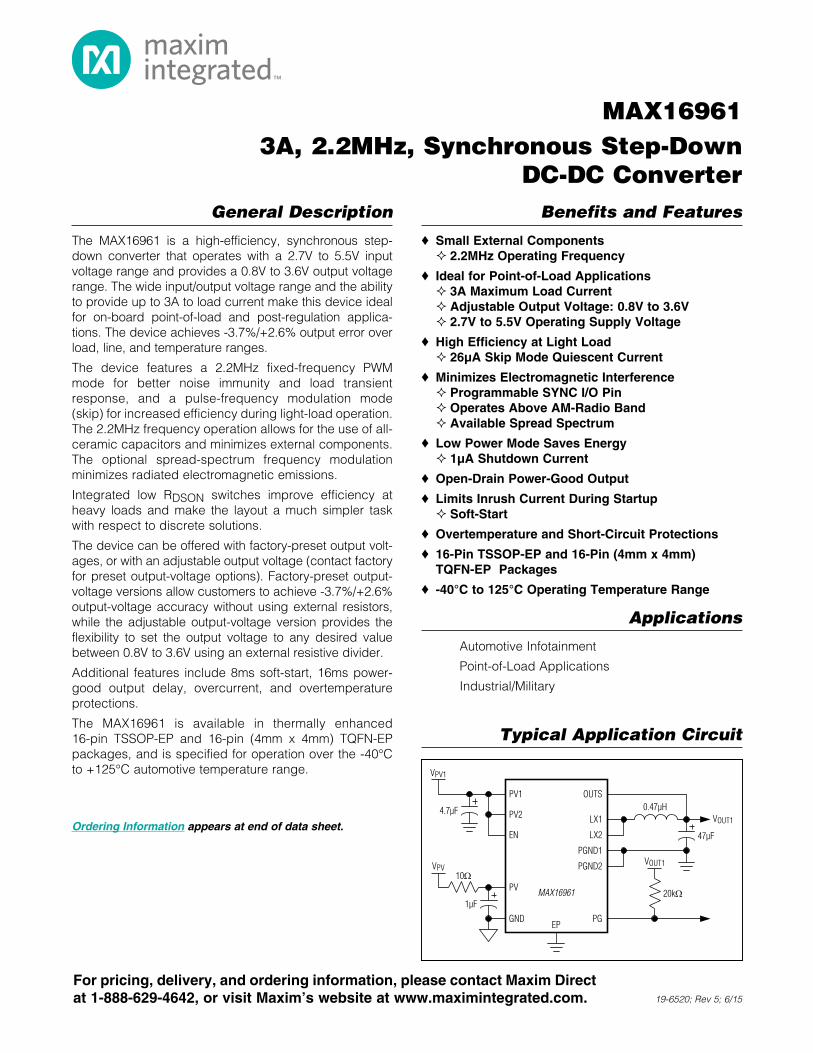
MAX16961 3A, 2.2MHz, Synchronous Step-Down DC-DC Converter General Description The MAX16961 is a high-efficiency, synchronous step- down converter that operates with a 2.7V to 5.5V input voltage range and provides a 0.8V to 3.6V output voltage range. The wide input/output voltage range and the ability to provide up to 3A to load current make this device ideal for on-board point-of-load and post-regulation applica- tions. The device achieves -3.7%/+2.6% output error over load, line, and temperature ranges. The device features a 2.2MHz fixed-frequency PWM mode for better noise immunity and load transient response, and a pulse-frequency modulation mode (skip) for increased efficiency during light-load operation. The 2.2MHz frequency operation allows for the use of all- ceramic capacitors and minimizes external components. The optional spread-spectrum frequency modulation minimizes radiated electromagnetic emissions. Integrated low R DSON switches improve efficiency at heavy loads and make the layout a much simpler task with respect to discrete solutions. The device can be offered with factory-preset output volt- ages, or with an adjustable output voltage (contact factory for preset output-voltage options). Factory-preset output- voltage versions allow customers to achieve -3.7%/+2.6% output-voltage accuracy without using external resistors, while the adjustable output-voltage version provides the flexibility to set the output voltage to any desired value between 0.8V to 3.6V using an external resistive divider. Additional features include 8ms soft-start, 16ms power- good output delay, overcurrent, and overtemperature protections. The MAX16961 is available in thermally enhanced 16-pin TSSOP-EP and 16-pin (4mm x 4mm) TQFN-EP packages, and is specified for operation over the -40NC to +125NC automotive temperature range. Benefits and Features S Small External Components 2.2MHz Operating Frequency S Ideal for Point-of-Load Applications 3A Maximum Load Current Adjustable Output Voltage: 0.8V to 3.6V 2.7V to 5.5V Operating Supply Voltage S High Efficiency at Light Load 26µA Skip Mode Quiescent Current S Minimizes Electromagnetic Interference Programmable SYNC I/O Pin Operates Above AM-Radio Band Available Spread Spectrum S Low Power Mode Saves Energy 1µA Shutdown Current S Open-Drain Power-Good Output S Limits Inrush Current During Startup Soft-Start S Overtemperature and Short-Circuit Protections S 16-Pin TSSOP-EP and 16-Pin (4mm x 4mm) TQFN-EP Packages S -40°C to 125°C Operating Temperature Range Applications Automotive Infotainment Point-of-Load Applications Industrial/Military Typical Application Circuit 19-6520; Rev 5; 6/15 Ordering Information appears at end of data sheet. MAX16961 OUTS PV1 LX1 PGND1 PG EP PGND2 LX2 0.47μH 47μF 20kΩ 10Ω 4.7μF 1μF V PV1 V OUT1 PV2 GND PV EN V PV V OUT1 For pricing, delivery, and ordering information, please contact Maxim Direct at 1-888-629-4642, or visit Maxim’s website at www.maximintegrated.com.

Welcome message from author
This document is posted to help you gain knowledge. Please leave a comment to let me know what you think about it! Share it to your friends and learn new things together.
Transcript
MAX169613A, 2.2MHz, Synchronous Step-Down
DC-DC ConverterGeneral Description
The MAX16961 is a high-efficiency, synchronous step-down converter that operates with a 2.7V to 5.5V input voltage range and provides a 0.8V to 3.6V output voltage range. The wide input/output voltage range and the ability to provide up to 3A to load current make this device ideal for on-board point-of-load and post-regulation applica-tions. The device achieves -3.7%/+2.6% output error over load, line, and temperature ranges.
The device features a 2.2MHz fixed-frequency PWM mode for better noise immunity and load transient response, and a pulse-frequency modulation mode (skip) for increased efficiency during light-load operation. The 2.2MHz frequency operation allows for the use of all-ceramic capacitors and minimizes external components. The optional spread-spectrum frequency modulation minimizes radiated electromagnetic emissions.
Integrated low RDSON switches improve efficiency at heavy loads and make the layout a much simpler task with respect to discrete solutions.
The device can be offered with factory-preset output volt-ages, or with an adjustable output voltage (contact factory for preset output-voltage options). Factory-preset output-voltage versions allow customers to achieve -3.7%/+2.6% output-voltage accuracy without using external resistors, while the adjustable output-voltage version provides the flexibility to set the output voltage to any desired value between 0.8V to 3.6V using an external resistive divider.
Additional features include 8ms soft-start, 16ms power-good output delay, overcurrent, and overtemperature protections.
The MAX16961 is available in thermally enhanced 16-pin TSSOP-EP and 16-pin (4mm x 4mm) TQFN-EP packages, and is specified for operation over the -40NC to +125NC automotive temperature range.
Benefits and Features
S Small External Components 2.2MHz Operating Frequency
S Ideal for Point-of-Load Applications 3A Maximum Load Current Adjustable Output Voltage: 0.8V to 3.6V 2.7V to 5.5V Operating Supply Voltage
S High Efficiency at Light Load 26µA Skip Mode Quiescent Current
S Minimizes Electromagnetic Interference Programmable SYNC I/O Pin Operates Above AM-Radio Band Available Spread Spectrum
S Low Power Mode Saves Energy 1µA Shutdown Current
S Open-Drain Power-Good Output
S Limits Inrush Current During Startup Soft-Start
S Overtemperature and Short-Circuit Protections
S 16-Pin TSSOP-EP and 16-Pin (4mm x 4mm) TQFN-EP Packages
S -40°C to 125°C Operating Temperature Range
Applications
Automotive Infotainment
Point-of-Load Applications
Industrial/Military
Typical Application Circuit
19-6520; Rev 5; 6/15
Ordering Information appears at end of data sheet.
MAX16961
OUTSPV1
LX1
PGND1
PGEP
PGND2
LX2
0.47µH
47µF
20kΩ
10Ω
4.7µF
1µF
VPV1
VOUT1PV2
GND
PV
EN
VPVVOUT1
For pricing, delivery, and ordering information, please contact Maxim Direct at 1-888-629-4642, or visit Maxim’s website at www.maximintegrated.com.
MAX169613A, 2.2MHz, Synchronous Step-Down
DC-DC Converter
2Maxim Integrated
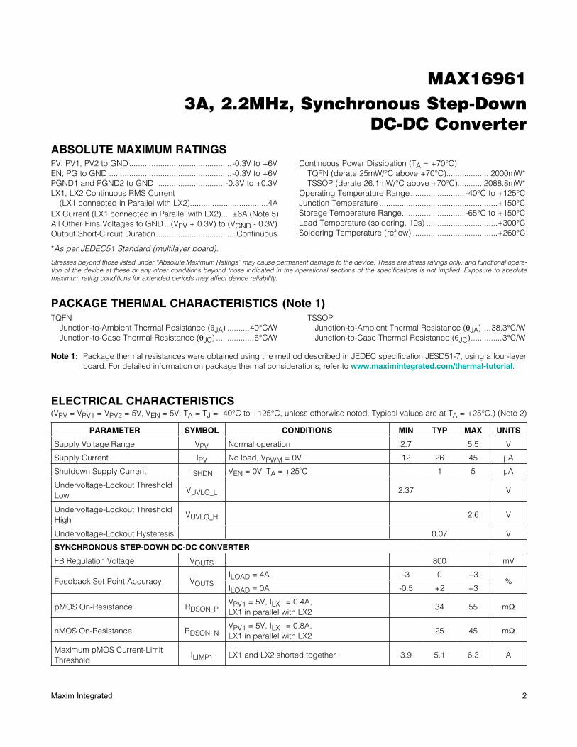
PV, PV1, PV2 to GND ..............................................-0.3V to +6VEN, PG to GND .......................................................-0.3V to +6VPGND1 and PGND2 to GND ..............................-0.3V to +0.3VLX1, LX2 Continuous RMS Current (LX1 connected in Parallel with LX2) ...................................4ALX Current (LX1 connected in Parallel with LX2).....Q6A (Note 5)All Other Pins Voltages to GND .. (VPV + 0.3V) to (VGND - 0.3V)Output Short-Circuit Duration ....................................Continuous
Continuous Power Dissipation (TA = +70NC) TQFN (derate 25mW/NC above +70NC)................... 2000mW* TSSOP (derate 26.1mW/NC above +70NC)........... 2088.8mW*
Operating Temperature Range ........................ -40NC to +125NCJunction Temperature .....................................................+150NCStorage Temperature Range ............................ -65NC to +150NCLead Temperature (soldering, 10s) ................................+300NCSoldering Temperature (reflow) ......................................+260NC
TQFN Junction-to-Ambient Thermal Resistance (BJA) ..........40NC/W Junction-to-Case Thermal Resistance (BJC) .................6NC/W
TSSOP Junction-to-Ambient Thermal Resistance (BJA) ....38.3NC/W Junction-to-Case Thermal Resistance (BJC) ..............3NC/W
ABSOLUTE MAXIMUM RATINGS
Note 1: Package thermal resistances were obtained using the method described in JEDEC specification JESD51-7, using a four-layer board. For detailed information on package thermal considerations, refer to www.maximintegrated.com/thermal-tutorial.
Stresses beyond those listed under “Absolute Maximum Ratings” may cause permanent damage to the device. These are stress ratings only, and functional opera-tion of the device at these or any other conditions beyond those indicated in the operational sections of the specifications is not implied. Exposure to absolute maximum rating conditions for extended periods may affect device reliability.
PACKAGE THERMAL CHARACTERISTICS (Note 1)
ELECTRICAL CHARACTERISTICS(VPV = VPV1 = VPV2 = 5V, VEN = 5V, TA = TJ = -40°C to +125°C, unless otherwise noted. Typical values are at TA = +25°C.) (Note 2)
*As per JEDEC51 Standard (multilayer board).
PARAMETER SYMBOL CONDITIONS MIN TYP MAX UNITS
Supply Voltage Range VPV Normal operation 2.7 5.5 V
Supply Current IPV No load, VPWM = 0V 12 26 45 FA
Shutdown Supply Current ISHDN VEN = 0V, TA = +25°C 1 5 FA
Undervoltage-Lockout Threshold Low
VUVLO_L 2.37 V
Undervoltage-Lockout Threshold High
VUVLO_H 2.6 V
Undervoltage-Lockout Hysteresis 0.07 V
SYNCHRONOUS STEP-DOWN DC-DC CONVERTER
FB Regulation Voltage VOUTS 800 mV
Feedback Set-Point Accuracy VOUTSILOAD = 4A -3 0 +3
%ILOAD = 0A -0.5 +2 +3
pMOS On-Resistance RDSON_PVPV1 = 5V, ILX_ = 0.4A, LX1 in parallel with LX2
34 55 mI
nMOS On-Resistance RDSON_NVPV1 = 5V, ILX_ = 0.8A,LX1 in parallel with LX2
25 45 mI
Maximum pMOS Current-Limit Threshold
ILIMP1 LX1 and LX2 shorted together 3.9 5.1 6.3 A
MAX169613A, 2.2MHz, Synchronous Step-Down
DC-DC Converter
3Maxim Integrated
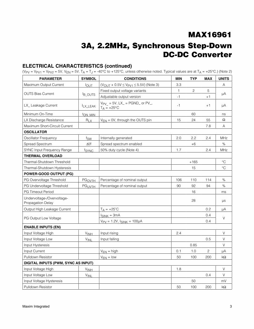
ELECTRICAL CHARACTERISTICS (continued)(VPV = VPV1 = VPV2 = 5V, VEN = 5V, TA = TJ = -40°C to +125°C, unless otherwise noted. Typical values are at TA = +25°C.) (Note 2)
PARAMETER SYMBOL CONDITIONS MIN TYP MAX UNITS
Maximum Output Current IOUT (VOUT + 0.5V P VPV1 P 5.5V) (Note 3) 3.3 A
OUTS Bias Current IB_OUTSFixed output voltage variants 1 2 5
FAAdjustable output version -1 +1
LX_ Leakage Current ILX_LEAKVPV_ = 5V, LX_ = PGND_ or PV_,TA = +25°C
-1 +1 FA
Minimum On-Time tON_MIN 60 ns
LX Discharge Resistance RLX VEN = 0V, through the OUTS pin 15 24 55 I
Maximum Short-Circuit Current 7.8 A
OSCILLATOR
Oscillator Frequency fSW Internally generated 2.0 2.2 2.4 MHz
Spread Spectrum Df/f Spread spectrum enabled +6 %
SYNC Input Frequency Range fSYNC 50% duty cycle (Note 4) 1.7 2.4 MHz
THERMAL OVERLOAD
Thermal-Shutdown Threshold +165 °C
Thermal-Shutdown Hysteresis 15 °C
POWER-GOOD OUTPUT (PG)
PG Overvoltage Threshold PGOVTH Percentage of nominal output 106 110 114 %
PG Undervoltage Threshold PGUVTH Percentage of nominal output 90 92 94 %
PG Timeout Period 16 ms
Undervoltage-/Overvoltage-Propagation Delay
28 Fs
Output High Leakage Current TA = +25°C 0.2 FA
PG Output Low VoltageISINK = 3mA 0.4
VVPV = 1.2V, ISINK = 100FA 0.4
ENABLE INPUTS (EN)
Input Voltage High VINH Input rising 2.4 V
Input Voltage Low VINL Input falling 0.5 V
Input Hysteresis 0.85 V
Input Current VEN = high 0.1 1.0 2 FA
Pulldown Resistor VEN = low 50 100 200 kI
DIGITAL INPUTS (PWM, SYNC AS INPUT)
Input Voltage High VINH 1.8 V
Input Voltage Low VINL 0.4 V
Input Voltage Hysteresis 50 mV
Pulldown Resistor 50 100 200 kI
MAX169613A, 2.2MHz, Synchronous Step-Down
DC-DC Converter
4Maxim Integrated
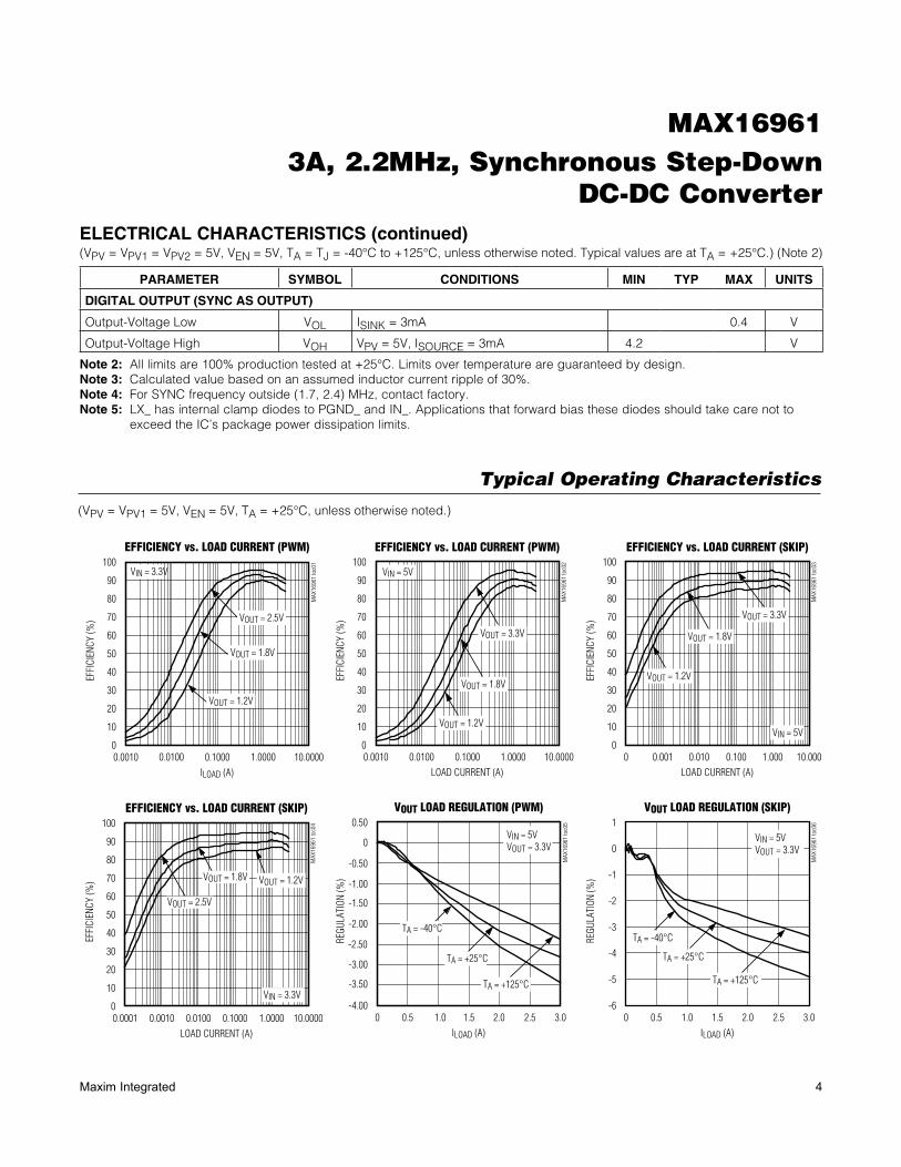
Typical Operating Characteristics
(VPV = VPV1 = 5V, VEN = 5V, TA = +25°C, unless otherwise noted.)
ELECTRICAL CHARACTERISTICS (continued)(VPV = VPV1 = VPV2 = 5V, VEN = 5V, TA = TJ = -40°C to +125°C, unless otherwise noted. Typical values are at TA = +25°C.) (Note 2)
Note 2: All limits are 100% production tested at +25°C. Limits over temperature are guaranteed by design.Note 3: Calculated value based on an assumed inductor current ripple of 30%.Note 4: For SYNC frequency outside (1.7, 2.4) MHz, contact factory.Note 5: LX_ has internal clamp diodes to PGND_ and IN_. Applications that forward bias these diodes should take care not to
exceed the IC’s package power dissipation limits.
PARAMETER SYMBOL CONDITIONS MIN TYP MAX UNITS
DIGITAL OUTPUT (SYNC AS OUTPUT)
Output-Voltage Low VOL ISINK = 3mA 0.4 V
Output-Voltage High VOH VPV = 5V, ISOURCE = 3mA 4.2 V
EFFICIENCY vs. LOAD CURRENT (PWM)
MAX
1696
1 to
c01
ILOAD (A)
EFFI
CIEN
CY (%
)
1.00000.10000.0100
10
20
30
40
50
60
70
80
90
100
00.0010 10.0000
VIN = 3.3V
VOUT = 1.2V
VOUT = 1.8V
VOUT = 2.5V
EFFICIENCY vs. LOAD CURRENT (PWM)M
AX16
961
toc0
2
LOAD CURRENT (A)
1.00000.10000.01000.0010 10.0000
EFFI
CIEN
CY (%
)
10
20
30
40
50
60
70
80
90
100
0
VOUT = 1.2V
VOUT = 3.3V
VOUT = 1.8V
VIN = 5V
EFFICIENCY vs. LOAD CURRENT (SKIP)
MAX
1696
1 to
c03
LOAD CURRENT (A)
1.0000.1000.0100.0010 10.000
EFFI
CIEN
CY (%
)
10
20
30
40
50
60
70
80
90
100
0
VOUT = 1.2V
VOUT = 3.3V
VOUT = 1.8V
VIN = 5V
EFFICIENCY vs. LOAD CURRENT (SKIP)
MAX
1696
1 to
c04
LOAD CURRENT (A)
EFFI
CIEN
CY (%
)
1.00000.10000.01000.0010
10
20
30
40
50
60
70
80
90
100
00.0001 10.0000
VIN = 3.3V
VOUT = 2.5V
VOUT = 1.8V VOUT = 1.2V
VOUT LOAD REGULATION (PWM)
MAX
1696
1 to
c05
ILOAD (A)
REGU
LATI
ON (%
)
2.52.01.51.00.5
-3.00
-3.50
-2.50
-1.50
-2.00
-0.50
-1.00
0
0.50
-4.000 3.0
VIN = 5VVOUT = 3.3V
TA = +25°C
TA = +125°C
TA = -40°C
VOUT LOAD REGULATION (SKIP)M
AX16
961
toc0
6
ILOAD (A)
REGU
LATI
ON (%
)
2.52.01.51.00.5
-5
-4
-3
-2
-1
0
1
-60 3.0
VIN = 5VVOUT = 3.3V
TA = +25°C
TA = +125°C
TA = -40°C
MAX169613A, 2.2MHz, Synchronous Step-Down
DC-DC Converter
5Maxim Integrated
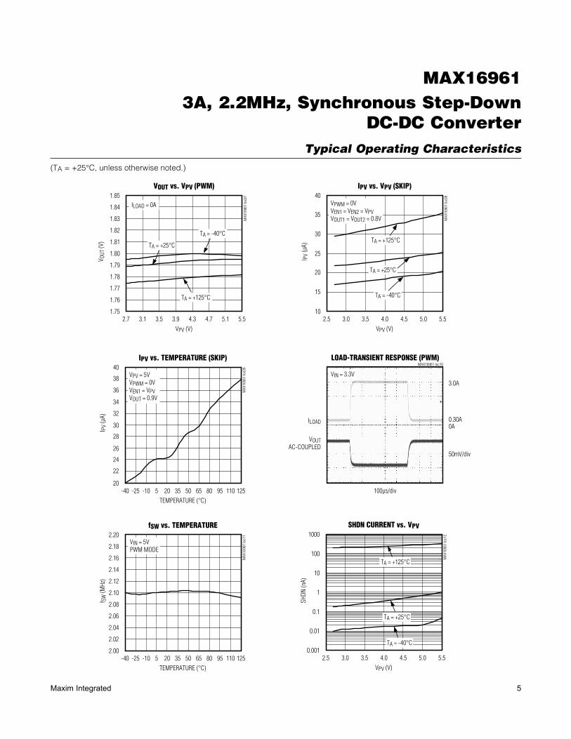
Typical Operating Characteristics(TA = +25°C, unless otherwise noted.)
VOUT vs. VPV (PWM)
MAX
1696
1 to
c07
VPV (V)
V OUT
(V)
5.14.73.9 4.33.53.1
1.76
1.77
1.78
1.79
1.80
1.81
1.82
1.83
1.84
1.85
1.752.7 5.5
TA = +25°C
TA = -40°C
TA = +125°C
ILOAD = 0A
IPV vs. VPV (SKIP)
MAX
1696
1 to
c08
VPV (V)
I PV
(µA)
5.04.54.03.53.0
15
20
25
30
35
40
102.5 5.5
VPWM = 0VVEN1 = VEN2 = VPVVOUT1 = VOUT2 = 0.8V
TA = +125°C
TA = +25°C
TA = -40°C
IPV vs. TEMPERATURE (SKIP)
MAX
1696
1 to
c09
TEMPERATURE (°C)
I PV
(µA)
11095-25 -10 5 35 50 6520 80
24
22
26
28
30
32
36
34
38
40
20-40 125
VPV = 5VVPWM = 0VVEN1 = VPVVOUT = 0.9V
LOAD-TRANSIENT RESPONSE (PWM)MAX16961 toc10
3.0A
0.30A0A
50mV/div
VOUTAC-COUPLED
ILOAD
100µs/div
VIN = 3.3V
fSW vs. TEMPERATURE
MAX
1696
1 to
c11
TEMPERATURE (°C)
f SW
(MHz
)
1109565 80-10 5 20 35 50-25
2.02
2.04
2.06
2.08
2.10
2.12
2.14
2.16
2.18
2.20
2.00-40 125
VIN = 5VPWM MODE
SHDN CURRENT vs. VPV
MAX
1696
1 to
c12
VPV (V)
SHDN
(nA)
5.04.54.03.53.0
0.01
0.1
1
10
100
1000
0.0012.5 5.5
TA = -40°C
TA = +25°C
TA = +125°C
MAX169613A, 2.2MHz, Synchronous Step-Down
DC-DC Converter
6Maxim Integrated
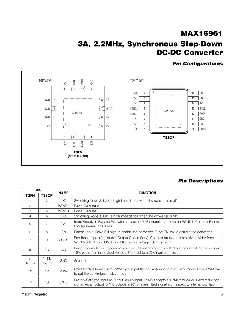
Pin Configurations
Pin Descriptions
PINNAME FUNCTION
TQFN TSSOP
1 3 LX2 Switching Node 2. LX2 is high impedance when the converter is off.
2 4 PGND2 Power Ground 2
3 5 PGND1 Power Ground 1
4 6 LX1 Switching Node 1. LX1 is high impedance when the converter is off.
5 7 PV1Input Supply 1. Bypass PV1 with at least a 4.7FF ceramic capacitor to PGND1. Connect PV1 to PV2 for normal operation.
6 8 EN Enable Input. Drive EN high to enable the converter. Drive EN low to disable the converter.
7 9 OUTSFeedback Input (Adjustable Output Option Only). Connect an external resistive divider from VOUT to OUTS and GND to set the output voltage. See Figure 2.
8 10 PGPower-Good Output. Open-drain output. PG asserts when VOUT drops below 8% or rises above 10% of the nominal output voltage. Connect to a 20kI pullup resistor.
9, 13–15
1, 11, 15, 16
GND Ground
10 12 PWMPWM Control Input. Drive PWM high to put the converters in forced-PWM mode. Drive PWM low to put the converters in skip mode.
11 13 SYNCFactory-Set Sync Input or Output. As an input, SYNC accepts a 1.7MHz to 2.4MHz external clock signal. As an output, SYNC outputs a 90° phase-shifted signal with respect to internal oscillator.
15
16
14
13
6
5
7
PGND
2
LX1
8
LX2
SYNC
GND
PV
1 2
GND
4
12 11 9
GND
PV2
PG
OUTS
EN
PV1+
PGND
1PW
M
3
10
GND
TQFN(4mm x 4mm)
TOP VIEW
+
TSSOP
134 SYNCPGND2
143 PVLX2
152 GNDPV2
161 GNDGND
107 PGPV1
116 GNDLX1
98 OUTSEN
125 PWMPGND1
EPEP
TOP VIEW
MAX16961MAX16961
MAX169613A, 2.2MHz, Synchronous Step-Down
DC-DC Converter
7Maxim Integrated
Pin Descriptions (continued)
Detailed Description
The MAX16961 is a high-efficiency, synchronous step-down converter that operates with a 2.7V to 5.5V input voltage range and provides a 0.8V to 3.6V output voltage range. The device delivers up to 3A of load current and achieves -3.7%/+2.6% output error over load, line, and temperature ranges.
The PWM input forces the device into either a fixed-frequency, 2.2MHz PWM mode or a low-power pulse- frequency modulation mode (skip). Optional spread-spectrum frequency modulation minimizes radiated electromagnetic emissions due to the switching frequency. The factory-programmable synchronization I/O (SYNC) enables system synchronization.
Integrated low RDSON switches help improve efficiency at heavy loads and make the layout a much simpler task with respect to discrete solutions.
The device is offered with factory-preset output voltages that achieve -3.7%/+2.6% output-voltage accuracy without using external resistors. In addition, the output voltage can be set to any desired values between 0.8V to 3.6V using an external resistive divider with the adjustable option.
Additional features include 8ms soft-start, 16ms power-good delay output, overcurrent, and overtemperature protections. See Figure 1.
Power-Good Output (PG)The device features an open-drain power-good output that asserts when the output voltage drops 8% below or rises 10% above the regulated voltage. PG remains asserted for a fixed 16ms timeout period after the output rises up to its regulated voltage. Connect PG to OUTS with a 20kI resistor.
Soft-StartThe device includes an 8ms fixed soft-start time. Soft-start time limits startup inrush current by forcing the output voltage to ramp up over time towards its regulation point.
Spread-Spectrum OptionThe device featuring spread-spectrum (SS) operation varies the internal operating frequency up by SS = 6% relative to the internally generated operating frequency of 2.2MHz (typ). This function does not apply to externally applied oscillation frequency. The internal oscillator is frequency modulated with a 6% frequency deviation. See the Selector Guide for available options.
Synchronization (SYNC)SYNC is a factory-programmable I/O. See the Selector Guide for available options. When SYNC is configured as an input, a logic-high on PWM enables SYNC to accept signal frequency in the range of 1.7MHz < fSYNC < 2.4MHz. When SYNC is configured as an output, a logic-high on PWM enables SYNC to output a 90N phase-shifted signal with respect to internal oscillator.
Current-Limit/Short-Circuit ProtectionThe device features current limit that protects the device against short-circuit and overload conditions at the out-put. In the event of a short-circuit or overload condition, the high-side MOSFET remains on until the inductor current reaches the high-side MOSFET’s current-limit threshold. The converter then turns on the low-side MOSFET to allow the inductor current to ramp down. Once the inductor current crosses the low-side MOSFET current-limit threshold, the converter turns on the high-side MOSFET for minimum on-time period. This cycle repeats until the short or overload condition is removed.
PINNAME FUNCTION
TQFN TSSOP
12 14 PVDevice Supply Voltage Input. Bypass with at least a 1FF ceramic capacitor to GND. In addition, connect a 10I decoupling resistor between PV and the bypass capacitor.
16 2 PV2Input Supply 2. Bypass PV2 with at least a 4.7FF ceramic capacitor to PGND2. Connect PV2 to PV1 for normal operation.
— — EPExposed Pad. Connect EP to a large-area contiguous copper ground plane for effective power dissipation. Do not use EP as the only IC ground connection. EP must be connected to GND.
MAX169613A, 2.2MHz, Synchronous Step-Down
DC-DC Converter
8Maxim Integrated
Figure 1. Internal Block Diagram
FPWM/Skip ModesThe device features an input (PWM) that puts the converter either in skip mode or forced-PWM (FPWM)mode of operation. See the Pin Descriptions section for mode details. In FPWM mode, the converter switches at a constant frequency with variable on-time. In skip mode, the converter’s switching frequency is load-dependent until the output load reaches the skip threshold. At higher load current, the switching frequency does not change and the operating mode is similar to the FPWM mode. Skip mode helps improve efficiency in light-load applications by allowing the converters to turn on
the high-side switch only when needed to maintain regulation. As such, the converter does not switch MOSFETs on and off as often as is the case in the FPWM mode. Consequently, the gate charge and switching losses are much lower in skip mode.
Overtemperature ProtectionThermal overload protection limits the total power dissipa-tion in the device. When the junction temperature exceeds +165°C (typ), an internal thermal sensor shuts down the internal bias regulator and the step-down controller, allowing the IC to cool. The thermal sensor turns on the IC again after the junction temperature cools by 15°C.
MAX16961
CONTROLLOGIC
STEP-DOWN
SKIP CURRENTCOMP
CURRENT-SENSEAMP
PEAK CURRENTCOMPRAMP
GENERATOR
PMWCOMP
CURRENT LIMCOMP
ERRORAMP FPWM
P1-OK
ZERO-CROSSINGCOMP
OUTS
SYNC
EN
P1-OK
PWM
PV
CLKPV1
PV1
PV2
LX1
LX2
PGND2
PGND1
PG
GND
PGND
CLK
CLK
FPWM
POWER-GOODCOMP
Σ
SOFT-STARTGENERATOR
VREF
VOLTAGEREFERENCE
TH-SD
FEEDBACKDRIVER
OSC.
MAINCONTROL
LOGIC
TRIM BITS
VREF
OTP
PV
PGND
MAX169613A, 2.2MHz, Synchronous Step-Down
DC-DC Converter
9Maxim Integrated
Applications Information
Setting the Output VoltageConnect OUTS to VOUT for factory-programmed out-put voltage (see the Selector Guide). To set the output to other voltages between 0.8V and 3.6V, connect a resistive divider from output (VOUT) to OUTS to GND (Figure 2). Select R2 (OUTS to GND resistor) less than or equal to 100kI. Calculate R1 (VOUT to OUTS resistor) with the following equation:
= −
×
≤ Ω+
OUT
OUTS
VR1 R2 1
V
R1 R2where 7.5k
R1 R2
where VOUTS = 800mV (see the Electrical Characteristics table).
The external feedback resistive divider must be frequency compensated for proper operation. Place a capacitor across each resistor in the resistive-divider network. Use the following equation to determine the value of the capacitors:
=
R2C1 10pF
R1
Inductor SelectionThree key inductor parameters must be specified for operation with the MAX16961: inductance value (L), inductor saturation current (ISAT), and DC resistance (RDCR). Use the following formulas to determine the minimum inductor value:
( )= − × ××
OUT_MIN IN OUT_
IN OP
V 3L V V ( )
V f 3A
where fOP is the operating frequency. This value is 2.2MHz unless externally synchronized to a different frequency.
The next equation ensures that the inductor current downslope is less than the internal slope compensation. For this to be the case, the following equation needs to be satisfied:
− ≥m2
m2
where m2 is the inductor current downslope:
OUTVL
and -m is the slope compensation:
µ
MAX0.8 xIs
Solving for L:
µ= ×
×MIN2 OUTs
L V1.6 3A
The equation that provides the bigger inductor value must be chosen for proper operation:
LMIN = max(LMIN1, LMIN2)
The maximum inductor value recommended is twice the chosen value from the above formula.
LMAX = 2 x LMIN
Figure 2. Adjustable Output Voltage Setting
Table 1. Inductor Values vs. (VIN - VOUT)
VIN - VOUT (V) 5.0 to 3.3 5.0 to 2.5 5.0 to 1.5 3.3 to 0.8
INDUCTOR (µH) 0.8 0.6 0.47 0.33
MAX16962
OUTS
R1
R2
C1
VOUT
MAX169613A, 2.2MHz, Synchronous Step-Down
DC-DC Converter
10Maxim Integrated
The maximum inductor value must not exceed the calculated value from the above formula. This ensures that the current feedback loop receives the correct amount of current ripple for proper operation.
Input CapacitorThe input filter capacitor reduces peak currents drawn from the power source and reduces noise and voltage ripple on the input caused by the circuit’s switching.
The input capacitor RMS current requirement (IRMS) is defined by the following equation:
OUT PV1 OUTRMS LOAD(MAX)
PV1
V (V V )I I
V
−=
IRMS has a maximum value when the input voltage equals twice the output voltage (VPV1 = 2VOUT), so IRMS(MAX) = ILOAD(MAX)/2.
Choose an input capacitor that exhibits less than +10NC self-heating temperature rise at the RMS input current for optimal long-term reliability.
The input-voltage ripple is composed of DVQ (caused by the capacitor discharge) and DVESR (caused by the ESR of the capacitor). Use low-ESR ceramic capacitors with high ripple-current capability at the input. Assume the contribution from the ESR and capacitor discharge equal to 50%. Calculate the input capacitance and ESR required for a specified input voltage ripple using the following equations:
ESRIN
LOUT
VESR
II
2
∆=
∆+
where:PV1 OUT OUT
LPV1 SW
(V V ) VI
V f L− ×
∆ =× ×
and:OUT
INQ SW
I D(1 D)C
V f× −
=∆ ×
and
OUT
PV1
VD
V=
where IOUT is the maximum output current, and D is the duty cycle.
It is strongly recommended that a 4.7FF small footprint be placed close to PV1 and PV2 and a minimum of 100nF small footprint be placed close to PV. Using a small foot-print such as 0805 or smaller helps to reduce the total parasitic inductance.
Output CapacitorThe minimum capacitor required depends on output voltage, maximum device current capability, and the error-amplifier voltage gain. Use the following formula to determine the required output capacitor value:
× Ω
=π× ×
=π × ×
REF x EAMPOUT(MIN)
CO OUT x CS
OUT 167m
V GC
2 f V R
0.8Vx31.72 210kHz V
where fCO, the target crossover frequency, is 210kHz, GEAMP, the error-amplifier voltage gain, is 31.7V/V, and RCS is 167mΩ.
PCB Layout GuidelinesCareful PCB layout is critical to achieve low switching losses and clean, stable operation. Use a multilayer board whenever possible for better noise immunity and power dissipation. Follow these guidelines for good PCB layout:
1) Use a large contiguous copper plane under the device package. Ensure that all heat-dissipating components have adequate cooling. The bottom pad of the device must be soldered down to this copper plane for effective heat dissipation and maximizing the full power out of the device. Use multiple vias or a single large via in this plane for heat dissipation.
2) Isolate the power components and high-current path from the sensitive analog circuitry. This is essential to prevent any noise coupling into the analog signals.
3) Add small footprint blocking capacitors with low self-resonance frequency close to PV1, PV2, and PV.
4) Keep the high-current paths short, especially at the ground terminals. This practice is essential for stable, jitter-free operation. The high-current path composed of input capacitors at PV1, PV2, inductor, and the output capacitor should be as short as possible.
5) Keep the power traces and load connections short. This practice is essential for high efficiency. Use thick copper PCBs (2oz vs. 1oz) to enhance full-load efficiency.
MAX169613A, 2.2MHz, Synchronous Step-Down
DC-DC Converter
11Maxim Integrated
6) OUTS is sensitive to noise for devices with external feedback option. The resistive network (R1 and R2)and the capacitive network (C1 and C2) must be placed close to OUTS and far away from the LX_ node and high switching current paths. The ground node of R2 and C2 must be close to GND.
7) The ground connection for the analog and power section should be close to the IC. This keeps the ground current loops to a minimum. In cases where only one ground is used enough isolation between analog return signals and high power signals must be maintained.
Chip Information
PROCESS: BiCMOS
Package Information
For the latest package outline information and land patterns (foot-prints), go to www.maximintegrated.com/packages. Note that a “+”, “#”, or “-” in the package code indicates RoHS status only. Package drawings may show a different suffix character, but the drawing pertains to the package regardless of RoHS status.
PACKAGE TYPE
PACKAGE CODE
OUTLINE NO.
LAND PATTERN NO.
16 TQFN-EP T1644+4 21-0139 90-0070
16 TSSOP-EP U16E+3 21-0108 90-0120
MAX169613A, 2.2MHz, Synchronous Step-Down
DC-DC Converter
12Maxim Integrated
Ordering Information
Note: “_” is a package suffix placeholder for either “R” or “S”, as shown in the Selector Guide. The 2nd “_” is in the option suffix./V denotes an automotive qualified part.+Denotes a lead(Pb)-free/RoHS-compliant package.*EP = Exposed pad.
Selector Guide
Note: Contact the factory for variants with different output-voltage, spread-spectrum, and power-good delay time settings.
PART TEMP RANGE LOAD CURRENT CAPABILITY (A) PIN-PACKAGE
MAX16961_ATE_/V+ -40°C to +125°C 4 16 TQFN-EP*
MAX16961_AUE_/V+ -40°C to +125°C 4 16 TSSOP-EP*
ROOT PARTPACKAGE
SUFFIXOPTION SUFFIX
OUTPUT VOLTAGE
SPREAD SPECTRUM
SYNC IN/OUT
MAX16961 RAUE A/V+ Ext. Adj. Disabled In
MAX16961 SAUE A/V+ Ext. Adj. Enabled In
MAX16961 RATE A/V+ Ext. Adj. Disabled In
MAX16961 SATE A/V+ Ext. Adj. Enabled In

MAX169613A, 2.2MHz, Synchronous Step-Down
DC-DC Converter
Maxim Integrated cannot assume responsibility for use of any circuitry other than circuitry entirely embodied in a Maxim Integrated product. No circuit patent licenses are implied. Maxim Integrated reserves the right to change the circuitry and specifications without notice at any time. The parametric values (min and max limits) shown in the Electrical Characteristics table are guaranteed. Other parametric values quoted in this data sheet are provided for guidance.
Maxim Integrated 160 Rio Robles, San Jose, CA 95134 USA 1-408-601-1000 13© 2015 Maxim Integrated Products, Inc. Maxim Integrated and the Maxim Integrated logo are trademarks of Maxim Integrated Products, Inc.
Revision History
REVISIONNUMBER
REVISIONDATE
DESCRIPTIONPAGES
CHANGED
0 11/12 Initial release —
1 4/13 Added non-automotive parts to Selector Guide 11
2 9/13Updated input voltage high min spec and input voltage low max spec, Figure 2, equation, step 6 in the PCB Layout Guidelines section, and the Ordering Information
3–5, 10, 11
3 5/14Added FB regulation voltage specifications and updated VPV condition in Electrical Characteristics table; corrected equations and updated Table 2 in the Inductor Selection and Output Capacitor sections; updated Ordering Information
2, 3, 9–11
4 6/15Updated General Description section to make it clear that factory needs to be contacted for fixed output-voltage trim options
1
5 7/15Added formula to equation in the Setting the Output Voltage section, replaced the Output Capacitor section, and deleted Table 2
9, 10
Related Documents