inter M82916 Pi BUS INTERFACE UNIT Military • 32·Bit Host Interface • 16·Bit Pi Bus Implementation • Intelligent Host Interface Supports: - Processor Systems • Master and Slave, or Slave Only Operation -1/0 Processors - Bulk Memory - Discrete 110 Subsystems • Extensive Interrupt Handling • Military Temperature Range: 55°C to + 125°C (T c) • Error Detecting Operation • Supports Dual Redundant Pi Bus Operation • 164 Pin Ceramic Quad Flat Pack (CQFP) Package • High Performance CHMOS IV Process This data sheet is supplemented by a M82916 User's Manual, Intel literature number 271160-001. The M82916 User's Manual provides detailed information regarding hardware and software board design information. LAB21-16 LAB 15-00 LABPHI LABPLO LOB31-00 LOBPHI LOBPLO t.ACt.AOO2-00 LOCAL BUS BPCHK CONTROL UNIT iW RUSUS RUSEL TACK BUSREQ BUSGNT APE OPE CHERR t.AAE LBCLK OEVBUSY RST PRCHLT Tt.ARCLK INT2 INTl I f ETt.ACLK t.AASTER t.AOOE CONTROL CHAIN CONTROL INT CONTROL TABLE CONTROL INT CONTROL INTERNAL REGISTERS LABEL TABLE PARt.A OPERATIONAL PARt.A INTERFACE PARt.A RECEIVE BUFFER DATA UNK REGISTERS SYSTEt.A TIt.AER ON-CHIP t.AONITOR f I f VIE A,B,ETC LOGICAL 10 f I ETt.ASEL ETt.AINT ETt.At.AOOE ETt.AOIN ETt.AOOUT Figure 1. Block Diagram PIBUS 15-00 OATACHK PICYC02-00 CYCCHK PlACK 03-00 PIWAIT01-00 Pi BUS PIBR01-00 CONTROL UNIT t.AOOI004-00 t.AOOPAR PICLKA PICLKB ORVENA ORVENB BUSENA BUSENB 271139-1 Intel Corporation assumes no responsibility for the use of any circuitry other than circuitry embodied in an Intel product. No other circuit p'atent licenses are implied. Information contained herein supersedes previously published specifications on these devices from Intel. September 1990 © INTEL CORPORATION, 1990 Order Number: 271139-002

Welcome message from author
This document is posted to help you gain knowledge. Please leave a comment to let me know what you think about it! Share it to your friends and learn new things together.
Transcript

inter M82916
Pi BUS INTERFACE UNIT Military
• 32·Bit Host Interface • 16·Bit Pi Bus Implementation
• Intelligent Host Interface Supports: - Processor Systems
• Master and Slave, or Slave Only Operation
-1/0 Processors - Bulk Memory - Discrete 110 Subsystems
• Extensive Interrupt Handling
• Military Temperature Range: 55°C to + 125°C (T c)
• Error Detecting Operation
• Supports Dual Redundant Pi Bus Operation
• 164 Pin Ceramic Quad Flat Pack (CQFP) Package
• High Performance CHMOS IV Process This data sheet is supplemented by a M82916 User's Manual, Intel literature number 271160-001. The M82916 User's Manual provides detailed information regarding hardware and software board design information.
LAB21-16
LAB 15-00
LABPHI
LABPLO
LOB31-00
LOBPHI
LOBPLO
t.ACt.AOO2-00 LOCAL BUS
BPCHK CONTROL UNIT
iW RUSUS
RUSEL
TACK
BUSREQ
BUSGNT
APE
OPE
CHERR
t.AAE
LBCLK
OEVBUSY
RST
PRCHLT
Tt.ARCLK
INT2
INTl I f
ETt.ACLK
t.AASTER t.AOOE CONTROL
CHAIN CONTROL
INT CONTROL
TABLE CONTROL
INT CONTROL
INTERNAL REGISTERS
LABEL TABLE PARt.A OPERATIONAL PARt.A INTERFACE PARt.A
RECEIVE BUFFER
DATA UNK REGISTERS
SYSTEt.A TIt.AER
ON-CHIP t.AONITOR
f I f
VIE A,B,ETC LOGICAL 10
f I ETt.ASEL ETt.AINT ETt.At.AOOE ETt.AOIN ETt.AOOUT
Figure 1. Block Diagram
PIBUS 15-00
OATACHK
PICYC02-00
CYCCHK
PlACK 03-00
PIWAIT01-00
Pi BUS PIBR01-00
CONTROL UNIT t.AOOI004-00
t.AOOPAR
PICLKA
PICLKB
ORVENA
ORVENB
BUSENA
BUSENB
271139-1
Intel Corporation assumes no responsibility for the use of any circuitry other than circuitry embodied in an Intel product. No other circuit p'atent licenses are implied. Information contained herein supersedes previously published specifications on these devices from Intel. September 1990 © INTEL CORPORATION, 1990 Order Number: 271139-002

inter M82916
GENERAL DESCRIPTION The M82916 Pi Bus Interface Unit is a highly integrated CMOS IV VLSI device that maximizes the performance of a Pi Bus based multi-processor system. The Pi Bus Interface Unit (PBIU) is designed to implement the interface between the Pi Bus and an electronics module (see Figure 2). It handles all bus protocol and DMA functions necessary to off-load Pi Bus communication from the host CPU. This allows maximum. bus performance and subsequently increases system throughput.
The host system may be intelligent such as a proceSSing module or an I/O module containing an I/O processor, or it may be a bulk memory or discrete I/O subsystem. The M82916 interfaces to the Pi Bus through a set of Pi Bus transceivers.
The M82916 implements a i6-bit (Type 16), Error Detecting (Class ED) Pi Bus Protocol, and can function as a Master and Slave (MS) or as a Slave Only (SO). These features are defined by the Society of Automotive Engineers (SAE), and the Joint Integrated Avionics Working Group (JIAWG) Pi Bus specifications. The M82916 will function on a Pi Bus with a clock rate up to 12.5 MHz and can be operated asynchronously to the host interface.
LOCAL BUS OPERATION The M82916 communicates directly with Local Bus elements using either Direct Memory Access (DMA) or Register Update (RU) operations. DMA Read, Write and Read-Modify-Write sequences are used while processing Pi Bus messages, updating tables, and storing interrupt reports. Register Update sequences are used when the host processor is reading or writing the internal registers of the M82916. All Local Bus operations are pipelined with address before data and therefore require the use of external latches between the M82916 and the local memory.
The following sections describe bus activity on the Local Bus. Each form of bus cycles is described in detail. The interface signals associated with the bus cycle are shown. The relationship between the signals themselves and between the signals and the Local Bus clock are indicated. For exact timing relationships refer to the electrical specification section at the end of the data sheet. All signals output from the PBIU are generated on the riSing edge of LBCLK. The Local Address Bus (LAB) and Memory Command Bus (MCMD) are driven active from the BUSGNT going low.
HOST SUBSYSTEM
~
MODULE=::; SLAVE
10
DRIVER .-< DlABLE
PICLKA
I CLOCK I RECEIVER
CLOCK A
i'" ~ i'" • i" CONTROL EN BUS
LOCAL BUS (OPTIONAL USE)
:;. :;. :;.
1.482916 PI BUS INTER" ACE UNIT
BUS . i" BUS v ENABLE
PI ENABLE DRIVER
r-. BUS "V' ENABLE SIGNALS .--- --------,
~1 1 PiCD<li
PI BUS I TRANSCEIVERS l PI BUS J
TRANSCEIVERS
• i'" .. i'"
7' ~ 7' PI BUSA PI BUS B
Figure 2. System Overview
2
l CLOCK RECEIVER
CLOCK B
J
271139-2
M82916
Abbreviations found in the figures are defined as follows:
SOURCE - Identifies the source of the associated signal/bus activity in the illustrated LBCLK period.
MI - Memory Interface Logic
PBIU - Pi Bus Interface Unit
RD - Read Command WR - Write Command
NOP - Null Command A, - Memory Address
D. - Memory Data
RU - Register Update
Several signal representations are used in the bus cycle figures to follow. Three logic levels are used: Logical one (high), Logical zero (low), and float (middle). Busses are shown active with simultaneous high and low levels with a bus value indicated between the levels. Busses shown active with no value indicated are in a don't care input state, or an unknown output condition. Individual input signals may be drawn similar to a bus with both a high and low level. This indicates a don't care time period for that input.
Transitions on outputs are illustrated with some delay, reflective of a real device. Input signals are illustrated at their minimum requirements. When an input signal is shown making a transition to a don't care state, the transition is optional.
Bus Acquisition The M82916 uses the BUSREQ and BUSGNT signals to arbitrate for control of the Local .Bus. BUSREQ is driven low by the M82916 when It requires control of the Lcoal Bus to perform a memory access. Local bus control is given to the M82916 when BUSGNT is driven low by either the host processor or some bus arbitration logic.
ACQUISITION WITH NO WAIT STATES
Figure 3 depicts a Bus Acquisition sequence for a two double-word (dword) memory read with no wait states. The bus cycle continues uninterrupted during a Bus Acquisition with no wait states. BUSGNT is driven low by the host's arbitration logic immediately following assertion of BUSREQ by the M82916. The address bus and Memory Command (MCMO) lines become active when BUSGNT goes low. The address is valid immediately, while the Memory Command lines are not valid until after the next rising edge of LBCLK.
TACK (MI) -f----t----t----t----T'''''----
LAB+--C~tt>___+_-MCMO--+-----<::g::::::~::::::~~---t_-----
LOB(MI) -,-----r---T" "' __ --,.'" "' __ --,.'" "' __ _ OPE, APE _J.... ___ ..I.. ___ """'"' ___ "'"' __ ~"'"' ,.----
MAE(MI) ....,r-----,....---T" "'--..... " .... ----,.'" "'---271139-3
Figure 3. Local Bus Acquisition with No Waits (Two dword Read)
3
M82916
BUSREQ is released by the PBIU at the end of the last address cycle (see Figure 3). This is the same time. the address and MCMO busses are placed in float. The M82916 uses a pipeline bus technique to provide the memory address one cycle before the data is required or provided. The bus cycle is completed when the last data word is acknowledged by TACK being low.
ACQUISITION WITH WAIT STATES
Figure 4 illustrates a Local Bus acquisition by the M82916 with wait states inserted. Two things can delay the M82916 from gaining control of the Local Bus. One is a delay of the BUSGNT signal to the PBIU. In Figure 4, BUSGNT is asserted one clock cycle after the request. The address bus and MCMO lines do not become active until BUSGNT is received. Additional wait states can be inserted by the arbiter or host processor by delaying BUSGNT even longer.
The second method wait states are added is by holding the TACK signal inactive (high). The LAB and MCMO busses are still driven active after grant Is received. LAB and MCMO do not change until the clock edge after TACK is low. The second cycle is the wait state. The wait state occurs because the Transfer Acknowledge signal is detected inactive at the end of the first cycle. When BUSGNT goes low the LAB and MCMO busses become active. The LOB does not become active until after the TACK signal is sampled low.
ACQUISITION WITH RE·ARBITRATION
A third situation can occur during bus acquisition or during the middle of a bus cycle. Local bus control can be taken away from the M82916. Figure 5 illustrates this situation. The arbiter or host processor granted bus control to the PBIU and then reversed its decision by de-asserting BUSGNT on the next clock. The LAB and MCMO busses are floated when BUSGNT becomes inactive (high). The bus cycle begins again when BUSGNT becomes active.
LBCLK -!l-!l-!l-!l-!l-!l-n-
TACK (MI)
LAB
MCMO
LOB (PBIU)
OPE,APE MAE(MI)
- 1\
I
\.
/ \. L
Al X A2
X WR
01 X 02
X VALID X VALID X I I I , , ,-
271139-4
Figure 4. Local Bus Acquisition with Walts (Two dword Write)
4
intJ M82916
LBCLK
MCMD--t------<::~~~_t------<:~:=::::~~::::::>-----_1--------LOB (PBIU) --t------+-------t-------1--------t-C::~~X:::§:::}------DPE.APE--~------~------~------~--------~.,-----~~r----~~'----
MAE (M!) --r-------...,..------..,...------__ --------~-----~-----_r_''---271139-5
Figure 5. Local Bus Acquisition with Re-Arbitration (Two dword Write)
DMA Operations The M82916 has a Direct Memory Access interface consisting of a 32-bit Local Data Bus (LOB) and a 22-bit Local Address Bus (LAB). Several control lines (BUSGNT, BUSREQ, BPCHK, MCMD, TACK, APE, OPE, and MAE) are also utilized during DMA operations. The Memory Command Bus determines the type of DMA operation that will be performed. Figure 6 identifies each possible operation.
MCMDBus Bus Cycle Type
02 01 00
0 0 0 dword DMA Write 0 0 1 Low word DMA Write 1 0 0 dword DMA Read 1 1 1 NOP
Figure 6. Memory Command Bus Decode
Error lines are utilized to provide fault tolerance in the host system. If the system detects an error duro ing DMA operations, the appropriate error signal must be active during the corresponding data cycle. The M82916 samples the error lines during data cycles only. Active error signals indicate address and data errors during the cycle in which they are sampled.
5
READ OPERATIONS
The DMA interface performs 32-bit wide single, double, triple, and quadruple double-word read operations (also called two, four, six and eight single word read operations). A double-word (dword) read (32 bits) will always be performed, even if the M82916 requires only a single word (16 bits) from memory. In the case of a single word read, the M82916 will correctly choose the required 16-bit word from the 32 bits of data.
The various types of DMA operations performed by the M82916's DMA interface are illustrated in the following figures. Unless otherwise specified, zero wait state operation is shown.
Single Dword Read
A single dword read operation is illustrated in Figure 7. The address cycle is one clock cycle after BUSGNT is received. The clock cycle following the address cycle is the data cycle. Data will be latched on the rising edge of the LBCLK (assuming TACK is low).

inter
Two Dword Read
M82916
TACK (MI) -+----~--~--+-----~~---
lAB~~----~~:::A~l~::~-------r--------
MCMO--~----~~l(::~~~-------r--------
LOB (MI) ....., ____ 1"""" ___ " .. 1"\. __ ....,."' ..... __ _
OPE, APE --..... ----..... -----"""-,.--........ ,.---
MAE(MI) --r----,-----r"''--....... ..;..,.''' ..... ---
Figure 7, One dword DMA Read (No Wait States)
Three Dword Read
271139-6
A two dword DMA read operation is depicted in Figure 8. As with a single dword access, the clock after BUSGNT becomes active is the first address cycle. The cycle following the first address cycle is the first data and the second address cycle. This allows the first address to be latched and remain active to the memory while the second address is driven out by the PBIU. The second data cycle is the last sequence of this operation.
Figure 9 illustrates the bus activity for a zero wait state three dword memory read. The BUSREQ signal is de-asserted by the M82916 at the same time the address and command busses become inactive. However, the bus cycle is not complete until after the last data cycle.
6

inter M82916
LBCLK
TACK{I.4I) -l----+--....J ..... +----+----+""----
LAB--t---~~==~~==~<=::~~}----t_----
I.4CI.40--t---~~~======~======~}----t_----LOB (I.4I)
~------~------~ OPE,APE--~---~----~,---~"---~,---I.4AE{1.41} -,-----T"'""----r-' ""----~ "---T""------
271139-7
Figure 8. Two dword DMA Read Operation (with No Wait States)
LBCLK
TACK{1.41} ~------~----~~------~----~------~-'----
LAB+---c:~~~:)---t--
I.4CI.40-1-----<:=~=====:====~~::=======:=>---1_----
LOB (I.4I) .....,----...----...,..,"---T"'--;.;.....,..'''-....;..;....., .. n.---OPE. APE -------'------""'1"--......... 1"--......... 1"--......... 1"---I.4AE{I.4I) .....,.---.....,----r-''"-....;;.;.....,.J,,_..;..;.~J,-....;;...;....,.J, ..... --
271139-8
Figure 9. Three dword DMA Read Operation (with No Wait States)
7
M82916
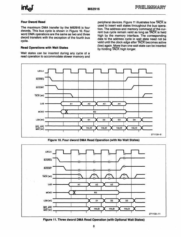
Four Dword Read
The maximum DMA transfer by the M82916 is four dwords. This bus cycle is shown in Figure 10. Four word DMA operations are the same as two and three dword transfers with the exception of the fourth bus cycle.
Read Operations with Wait States
Wait states can be inserted during any cycle of a read operation to accommodate slower memory and
LBCLK
peripheral devices. Figure 11 illustrates how TACK is used to insert wait states throughout the bus operation. The address and memory command of the current bus cycle remain valid as long as TACK is held high by the memory interface. The corresponding data to the address cycle in wait state need not be valid until the clock edge after TACK becomes active (low) again. More than one wait state can be inserted by holding TACK high longer.
TACK(IAI) -~---I--~-+----+----+----+----t-...... --
IACIAD-1r---~~c:::::~::::::~::::::~::::::~~---t-----LDB (1A1) --,.----,-----r''----r-' '--"";';;""-,J ' ..... --..,,...., '--;;""""T""'---
Figure 10. Four dword DMA Read Operation (with No Wait States)
LBCLK
TACK(IAI) -~---f--!s-::t.....t-I-~I-... t-"-~I-........ t-....... ~I---I---
IACIAD-1r----~~c:::::~::~::;:::::::;>----t_---
LDB(IAI) -r-----r----,....---,.... '----r-' .... --"T"
DPE.APE--~-----~----~r-~~~'--~~r-~~u IAAE(IAI) ....,----r----r''--=~r'' ...... =::..,-J\........;.;;;;:;;T'''---
Figure 11. Three dword DMA Read Operation (with Optional Wait States)
8
271139-9
271139-11
M82916
WRITE OPERATIONS
Write sequences can be one, two, three, four, five, six, seven, or eight single words in length. A write operation with an odd number of words will begin with a single word transfer, but all remaining words will be written in dword transfers. This type of transfer will begin with a single word write of the low word (LOB 15-00). A write operation may also end with a single word (odd word count). In this situation the last valid word will be written to the high word (LOB 32-16). Indeterminable data will be written to the low word.
Write operations for the M82916 follow the same sequence as the read operations described in the Read Operations section. The only differences between read and write operations are that the data bus is driven by the M82916 and the MCMO lines reflect a write operation. Wait states can be inserted into write operations using the same methods previously shown for read operations (see Figure 11). The data, address and memory command for write operations remain valid during the cycles in which wait states are inserted.
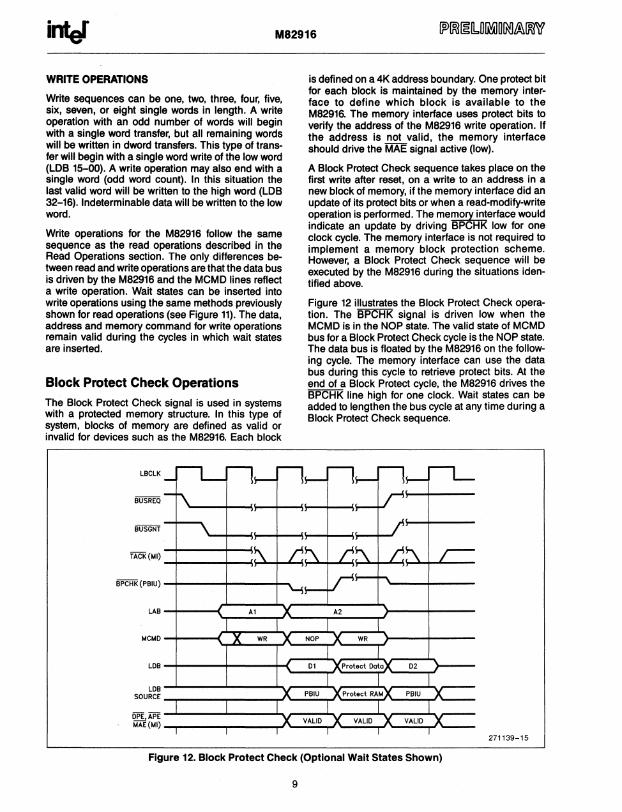
Block Protect Check Operations
The Block Protect Check signal is used in systems with a protected memory structure. In this type of system, blocks of memory are defined as valid or invalid for devices such as the M82916. Each block
- t"\
\
is defined on a 4K address boundary. One protect bit for each block is maintained by the memory interface to define which block is available to the M82916. The memory interface uses protect bits to verify the address of the M82916 write operation. If the address is not valid, the memory interface should drive the MAE signal active (low).
A Block Protect Check sequence takes place on the first write after reset, on a write to an address in a new block of memory, if the memory interface did an update of its protect bits or when a read-modify-write operation is performed. The memory interface would indicate an update by driving BPCHK low for one clock cycle. The memory interface is not required to implement a memory block protection scheme. However, a Block Protect Check sequence will be executed by the M82916 during the situations identified above.
Figure 12 illustrates the Block Protect Check operation. The BPCHK Signal is driven low when the MCMO is in the NOP state. The valid state of MCMD bus for a Block Protect Check cycle is the NOP state. The data bus is floated by the M82916 on the following cycle. The memory interface can use the data bus during this cycle to retrieve protect bits. At the end of a Block Protect cycle, the M82916 drives the BPCHK line high for one clock. Wait states can be added to lengthen the bus cycle at any time during a Block Protect Check sequence.
/
TACK (MI) ~\ ;;~ ;;~ ;;~ r-BPCHK (PBIU)
LAB
MCMD
LDB
LDB SOURCE
I
A1
~ WR
I
X
X NOP
D1
X PBIU
VALID
I
-I~
/
A2
.x WR
XProtect DataX D2
XProtect RAMX PBIU
.r---X VALID X VALID ~
I I I
Figure 12. Block Protect Check (Optional Wait States Shown)
9
271139-15

M82916
Read-Modify-Write Operations The M82916 can execute a read-modify-write (RMW) sequence to update a Single dword in memory. During a read-modify-write with no wait states, a read sequence is performed followed two LBCLK cycles later by a write sequence. Figure 13 illustrates this operation. The clocks between the read and write are spent bringing the data in, altering the data, then preparing the data to be sent back out on the Local Bus. This time is also used to perform a Block Protect Check sequence without any delay to the bus operation.
Read-modify-write sequences can also be performed with wait states. Figure 14 illustrates how a "free" wait state (with no additional clocks) can be inserted directly after the read of a RMW sequence. The TACK cycle postpones the BPCHK cycle until the third clock. This operation takes the same number of clocks to execute as a RMW sequence with no wait states.
Wait states can be added that lengthen a readmodify-write cycle. Figure 15 shows a wait state added to the read cycle. Wait states can also be added during other clock cycles within the RMW cycle.
LBCLK -!l-!l-!l-IL.!l-!l-n-
TACK (MI)
BPCHK (PBIU)
LAB
MCMO
LOB
LOB SOURCE
)
- r\
I
1
\.
J
A1
X RD J(. NOP X WR
Yo. ROD1 XProtect Doto
Yo. MI X Protect RAMX
I I 1 I .A VALID .x VALID X VALID
1 I 1 1 I
Figure 13. Read-Modify-Write (No Wait States)
10
r-
WRD2
Yo. PBIU X-1:=
.x VALID X ,-271139-16

M82916
LBCLK
TACK(t.tI) -I-----I--....J ..... +----+---'
BPCHK(PBIU) -,---t----T""'\. __ -4/----1I'---+----+----
LAB+---c~~==~:)----j--t.tCt.tO+--<:x::20c:~=x~--t-
LOB-~---~---~"--~~,--~"',~--~,---~~r----
SOURCE __ r-______ ~------~,~--~~J, ..... ---~'-~~~r'-~~_rJ'----OPE. APE - ..... ------.J...------...I..\.,----~~J..---~.I-V'---.....I ..... I'--....I. .....
t.tAE(t.t1) -,.....---,.....---~'""--T---"'I""---~---"'I""
LBCLK
TACK(t.t1)
BPCHK (PBIU)
LAB t.tCt.tO
LOB
LOB SOURCE
----
Figure 14. Read-Modify-Write (with "Free" Wait State)
!l-IL !LJ IL !l-IL..... 1\
\.
\. /
/
A1
X RO X NOP X WR
X ROO1 XProtect Oato
X t.tl X Protect RAt.t X
IL j
j
WR02
X PBIU
271139-17
!L..
~
}---
X---OPE. APE t.tAE(t.tI) X VALID X VALID X VALID X VALID ~
1-I I I I I I I
271139-18
Figure 15. Read-Modify-Write (with Wait State for Read Data)
11
intJ M82916
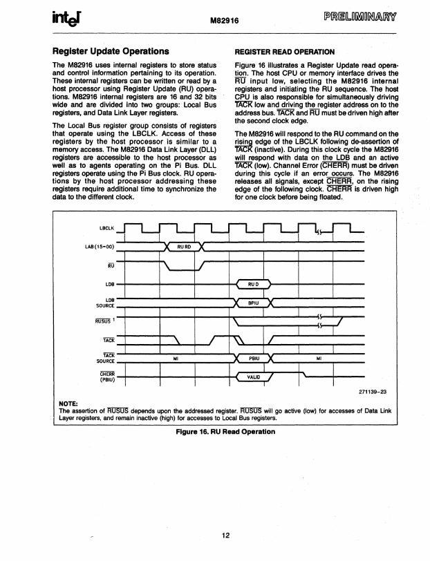
Register Update Operations
The M82916 uses internal registers to store status and control information pertaining to its operation. These internal registers can be written or read by a host processor using Register Update (RU) operations. M82916 internal registers are 16 and 32 bits wide and are divided into two groups: Local Bus registers, and Data Link Layer registers.
The Local Bus register group consists of registers that operate using the LBCLK. Access of these registers by the host processor is similar to a memory access. The M82916 Data Link Layer (DLL) registers are accessible to the host processor as we" as to agents operating on the Pi Bus. DLL registers operate using the Pi Bus clock. RU operations by the host processor addressing these registers require additional time to synchronize the data to the different clock.
NOTE:
LBCLK
L.t.B(15-00)
LOB
LOB SOURCE
T.t.CK SOURCE
CHERR (PBIU) I I
X RURO X
"- /
"- /
MI
I I
REGISTER READ OPERATION
Figure 16 illustrates a Register Update read operation. The host CPU or memory interface drives the RU input low, selecting the M82916 internal registers and initiating the RU sequence. The host CPU is also responsible for simultaneously driving TACK low and driving the register address on to the address bus. TACK and RU must be driven high after the second clock edge.
The M82916 wi" respond to the RU command on the riS@g edge of the LBCLK following de-assertion of TA K (inactive). During this clock cycle the M82916 wi" respond with data on the LOB and an active TACK (low). Channel Error (CHERR) must be driven during this cycle if an error occurs. The M82916 releases a" signals, except CHERR, on the rising edge of the following clock. CHERR is driven high for one clock before being floated.
~
RUO
X BPIU X
"- /
\.\. /
X PBIU X MI
V.t.LIO / I I I 271139-23
The assertion of RUSUS depends upon the addressed register. RUSUS will go active (low) for accesses of Data Link Layer registers, and remain inactive (high) for accesses to Local Bus registers.
Figure 16. RU Read Operation
12
M82916
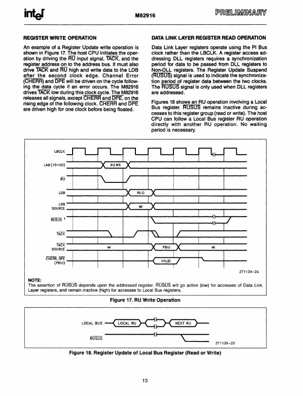
REGISTER WRITE OPERATION
An example of a Register Update write operation is shown in Figure 17. The host CPU initiates the operation by driving the RU input signal, TACK, and the register address on to the address bus. It must also drive TACK and RU high and write data to the LOB after the second clock edge. Channel Error (CHERR) and OPE will be driven on the cycle following the data cycle if an error occurs. The M82916 drives TACK low during this clock cycle. The M82916 releases all signals, except CHERR and OPE, on the rising edge of the following clock. CHERR and OPE are driven high for one clock before being floated.
LBCLK
DATA LINK LAYER REGISTER READ OPERATION
Data Link Layer registers operate using the Pi Bus clock rather than the LBCLK. A register access addressing OLL registers requires a synchronization period for data to be passed from OLL registers to Non-OLL registers. The Register Update Suspend (mTSUS) signal is used to indicate the synchronization period of register data between the two clocks. The RUSUS signal is only used when OLL registers are addressed.
Figures 18 shows an RU operation involving a Local Bus register. RiJSlJS remains inactive during accesses to this register group (read or write). The host CPU can follow a Local Bus register RU operation directly with another RU operation. No waiting period is necessary.
LAB (15-00) -r------r-' " __ ....,..." '"--....,...---....,...-----r-----r----
LDB~r__---r__---~·~~~rI~--~---~---~---LDB~----~---~.r_--~.r_--~---~---~---SOURCE __ r--___ r-___ rl"-~~T""---~---~---~----
TACK ~----r__-Jo--!_-'
~CK~----~---~----~r----~r---~---~---
SOURCE __ r--___ r-~~_r-___ ~·"-~~~'---~-~-~----
CHERR.DPE-~----r------r----t~~~~)T---r'----t----(PBIU) 271139-24
NOTE: The assertion of RUSUS depends upon the addressed register. RUSUS will go active (low) for accesses of Data Link Layer registers. and remain inactive (high) for accesses to Local Bus registers.
Figure 17. RU Write Operation
LOCAL BUS --< LOCAL RU >-<::!~ NEXT RU }--
II \ ...... -- 271139-20
Figure 18. Register Update of Local Bus Register (Read or Write)
13
inter M82916
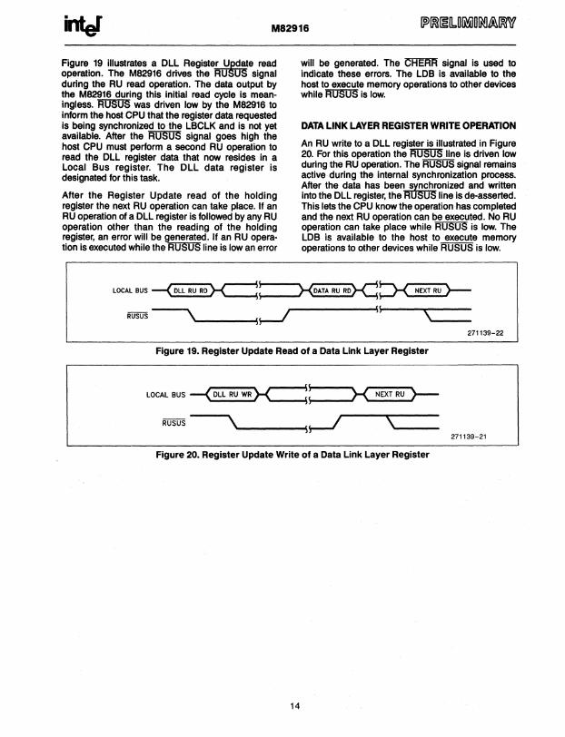
Figure 19 illustrates a Oll Register ~G8~e read operation. The M82916 drives the R Signal during the RU read operation. The data output by the M82916 during this initial read cycle is meaningless. ~ was driven low by the M82916 to inform the host CPU that the register data requested is being synchronized to the lBClK and is not yet available. After the RUSUS signal goes high the host CPU must perform a second RU operation to read the Oll register data that now resides in a local Bus register. The Oll data register is designated for this task.
After the Register Update read of the holding register the next RU operation can take place. If an RU operation of a Oll register is followed by any RU operation other than the reading of the holding register, an error will be generated. If an RU operation is executed while the RUSUS line is Iowan error
will be generated. The ~ signal is used to indicate these errors. The lOB is available to the host to execute memory operations to other devices while RU8U8 is low.
DATA LINK LAYER REGISTER WRITE OPERATION
An RU write to a Oll register is illustrated in Figure 20. For this operation the RU8US line is driven low during the RU operation. The RUSUS signal remains active during the internal synchronization process. After the data has been R~Sc~onized and written into the Oll register, the U line is de-asserted. This lets the CPU know the operation has completed and the next RU operation can be executed. No RU operation can take place while RU8U8 is low. The lOB is available to the host to execute memory operations to other devices while RUSUS is low.
LOCAL BUS --< OLL RU RO ~I-: __ -J}-{OATA RU RO>-<::::::>-< NEXT RU >--' .... -----IIs---!
II \ ..... --
271139-22
Figure 19. Register Update Read of a Data Link layer Register
LOCAL BUS --< DLL RU WR >-<'-__ ~:I-: __ --'>-< NEXT RU }--
\,---~\r---I ''--- 271139-21
Figure 20. Register Update Write of a Data Link layer Register
14

inter M82916
Pi BUS OPERATION
The Pi Bus protocol is implemented by the Pi Bus control unit of the MB2916. The MB2916 interfaces with the Pi Bus backplane through this functional block. This interface provides dual transceiver control signals for a redundant Pi Bus implementation. All Pi Bus protocol message handling, error handling, and error generation is performed by the MB2916. The intelligent control unit performs all the protocol tasks autonomous from the host CPU.
Pi Bus Master Mode Description
The MB2916 operates in the Master mode when it acquires Pi Bus mastership and begins to initiate messages. The Master mode is typically used when the MB2916 is the Pi Bus interface on an intelligent module such as an MB0960 processor module. The MB2916 operates out of a command chain located in local memory.
Each instruction in the chain defines a single message for the Pi Bus. The master retrieves the chain instruction, interprets the contents, and executes the
Add~::: --+----------1 Master Interrupt Queue
28 x 4 ~ 078h f------------1
Normal Command Cell +07Ch~-------~
Priority Command Cell +080hf--_______ ---1
specified operation within the instruction. The contents of the chain instruction specify features such as data buffer address, message transfer word count, store an interrupt report, inhibit message suspension, NOP instruction, jump instruction, and the header words of the Pi Bus message.
The PBIU uses several Local Bus memory resources when operating as a Pi Bus Master. These resources are:
• Master I nterrupt Queue
• Normal Command Cell
• Priority Command Cell
• Message Chains • Message Data Buffers
The Master mode local memory resources are shown in Figure 21. The interrupt queue and command cells are located at the base address specified in the Base Address register. The command cells contain the address of their respective message chains, with each chain instruction (where required) containing the address of the data buffer to be used for the message.
271139-25
Figure 21 . Master Mode Local Memory Resources
15
intJ M82916
Message chain instructions are used by the M82916 to initiate messages over the Pi Bus. The chain instructions contain the header words to be used for the message. The types of messages that the M82916 can execute are:
• Parameter Write, Single Slave
• Parameter Write, Multiple Slaves
• Block Message Write, Short Header, Single Slave
• Block Message Read, Short Header, Single Slave
• Block Message Write, Short Header, Multiple Slaves
• Tenure Pass
• Bus Interface Write, Single Slave
• Bus Interface Read, Single Slave
• Bus Interface Write, Multiple Slaves
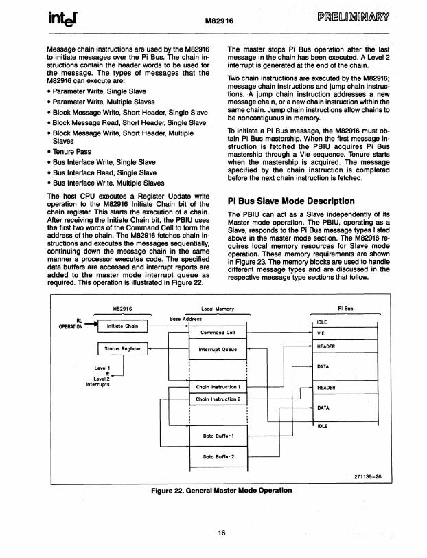
The host CPU executes a Register Update write operation to the M82916 Initiate Chain bit of the chain register. This starts the execution of a chain. After receiving the Initiate Chain bit, the PBIU uses the first two words of the Command Cell to form the address of the chain. The M82916 fetches chain instructions and executes the messages sequentially, continuing down the message chain in the same manner a processor executes code. The specified data buffers are accessed and interrupt reports are added to the master mode interrupt queue as required. This operation is illustrated in Figure 22.
The master stops Pi Bus operation after the last message in the chain has been executed. A Level 2 interrupt is generated at the end of the chain.
Two chain instructions are executed by the M82916; message chain instructions and jump chain instructions. A jump chain instruction addresses a new message chain, or a new chain instruction within the same chain. Jump chain instructions allow chains to be noncontiguous in memory.
To initiate a Pi Bus message, the M82916 must obtain Pi Bus mastership. When the first message instruction is fetched the PBIU acquires Pi Bus mastership through a Vie sequence. Tenure starts when the mastership is acquired. The message specified by the chain instruction is completed before the next chain instruction is fetched.
Pi Bus Slave Mode Description The PBIU can act as a Slave independently of its Master mode operation. The PBIU, operating as a Slave, responds to the Pi Bus message types listed above in the master mode section. The M82916 requires local memory resources for Slave mode operation. These memory requirements are shown in Figure 23. The memory blocks are used to handle different message types and are discussed in the respective message type sections that follow.
t.l82916 Locol Memory Pi Bus
RU OPERATION Inltlato Chain
I Statu. Roglster
Level~J Level 2
Interrupts
Base Address
,--- Command Cell
Interrupt Queue I---, , , , , , , ,
r--l Chain Instruction 1 J
Chain Instruction 2
, , , , , , , ,
Data Buffer 1
Data Buffer 2
Figure 22_ General Master Mode Operation
16
IDLE
VIE
HEADER
,-----. DATA
r HEADER
DATA
IDLE
271139-26

inter M82916
BAS E + 080h
BUFFER A
+ 100h 42 x 3
BUFFER B
+180h 42 x 3
BUFrER C
+ 200h 42 x 3
Slave Interrupt Queue 271139-27
Event Filter
BUFFER
BUFFER
• • •
EJ Direct Messages
Table ---,-----, Address
• • •
FILTER MAX
Parameter Write
Block Message Label Table ---,.-----,
Address
Block Messages, Label Type 271139-28
Figure 23. Slave Mode Memory Map
The Slave 10 field of the message must match the PBIU module 10, must address an enabled logical slave 10 or must be the broadcast address. The Slave identifies the message as pertinent when one of the addressing requirements has been met. The PBIU decodes the Message Type (MT) field of the header to determine if the message type is acceptable. The Access Type (AT) field is then decoded and compared with both the enabled and implemented access types to determine if the PBIU will respond to the message.
The Slave provides information regarding message operation to the host processor through interrupt reports. A three-buffer interrupt report queue is used to store these reports. Successful messages, unsuccessful messages, Pi Bus errors, and Local Bus errors are examples of the conditions for which an interrupt report would be generated.
The M82916 becomes Busy to Pi Bus messages when the slave interrupt queue becomes full or a Local Bus error is encountered during an access of local memory. Host action is required to clear the interrupt and hence remove the Busy condition. The PBIU also becomes busy following an Abort while it
17
is storing the interrupt report (if required). Once the interrupt report is stored, the M82916 becomes not Busy.
Pi BUS MESSAGES
Message types 0, 2 and 6 are reserved codes and do not have a defined Pi Bus sequence. The slave will consider them to be command errors in the Interrupt Report and Multiple Slave Acknowledge Word. The Slave will not respond to a reserved message.
BLOCK MESSAGES
Pi Bus modules use block messages as the work horse of the bus. Block messages are used to transfer blocks of data between two or more modules. Transfers up to 64K words long can be performed with a block message. Block messages are both read and write data transfers ..
The M82916 implements two types of block messages; direct and label type. These two block messages are identified by an access type in the message header word. Both are used to transfer blocks of data across the Pi Bus, but implement a different storage method within the Slave.

M82916
In direct type block messages the Pi Bus master specifies the data buffer address in the header words. This is the physical address of a data buffer in the Slave module. The sequence of a direct block message read transfer is shown in Figure 24. The header words are received by the slave and acknowledged by the addressed slave. The slave then uses the address in the header words to retrieve or store data transferred in the message. Any interrupt report is stored after the data acknowledge cycle. The memory resource needed for direct block messages is simply the data buffer.
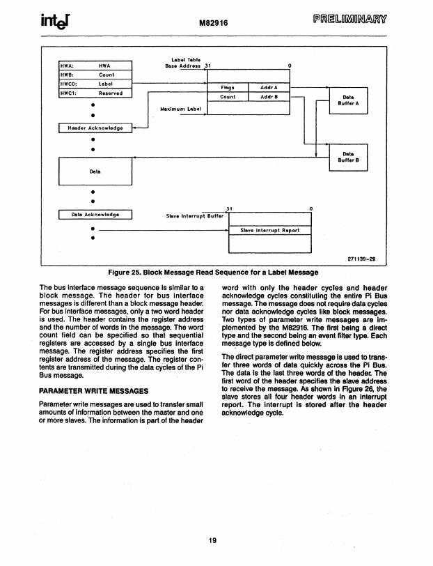
The second type of block message transfer is a label type. The sequence of this type of message is illustrated in Figure 25. This message type is much more flexible than the direct message. The header word contains a label instead of a physical address. The label is used to select a block from the Label Table in Local memory. The Slave uses the Label Table Entry to define the handling of the block message.
The Lable Table Entry contains four fields; flags, count, address A, and address B. The flags define
HWA: HWA
HW8: Count
HWCO: Data Buffer
HWC1: Address I--
• •
Header Acknowledge 1-• • Data.
• •
Data Acknowledge
• •
options available for the label. The count field specifies the number of words to be transferred in the block message. The two address fields define the location of two data buffers. These buffers can be used in a double buffering scheme through the control bits in the flag field.
The label type block message continues just as the direct type. The data is retrieved or stored in the data buffer available. Any interrupt report is stored in the slave interrupt queue after the data acknowledge cycle. Some updates to the label table entry may take place ai the end of the message depending on the options selected in the flags field.
BUS INTERFACE MESSAGES
Bus interface messages are used to access the Data link Layer registers of modules across the Pi Bus. A Pi Bus master can read or write the Data link Layer registers of slaves on the Pi Bus. The Data link Layer registers of the M82916 can be write protected against bus interface messages.
rl I Data
Buffer
Slave Interrupt Buffer 31 0
Slave Interrupt Report
271139-30
Figure 24. Block Message Read Sequence for a Direct Message
18
intJ M82916
HWA: HWA
HW8: Count
HWCO: Label
HWCI: Reserved
• •
Header Ack now ledge
• •
Oat.
• •
Label Tabl. Base Address 31
Maximum lflbal -J--
0
nogs I AddrA
Count 1 Addr8 Oata - ,- Buffer A
Oata Buffor B
31 o Data Acknowledge Slave Interrupt Buffer
• ----------------------------t==§s~~Y~e~ln~t~er~ru~p~t!R;.p~o~rtc=~ •
271139-29
Figure 25. Block Message Read Sequence for a Label Message
The bus interface message sequence Is similar to a block message. The header for bus interface messages is different than a block message header. For bus interface messages, only a two word header is used. The header contains the register address and the number of words in the message. The word count field can be specified so that sequential registers are accessed by a single bus interface message. The register address specifies the first register address of the message. The register con· tents are transmitted during the data cycles of the Pi Bus message.
PARAMETER WRITE MESSAGES
Parameter write messages are used to transfer small amounts of information between the master and one or more slaves. The information is part of the header
19
word with only the header cycles and header acknowledge cycles constituting the entire PI Bus message. The message does not require data cycles nor data acknowledge cycles like block messages. Two types of parameter write messages are implemented by the M82916. The first being a direct type and the second being an event filter type. Each mes.sage type is defined below.
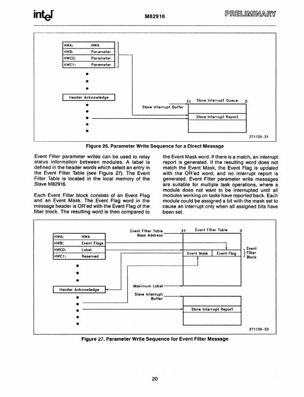
The direct parameter write message is used to transfer three words of data quickly across the Pi Bus. The data is the last three words of the header. The first word of the header specifies the slave address to receive the message. As shown In Figure 26, the slave stores all four header words In an Interru~ report. The interrupt is stored after the header acknowledge cycle.
inter M82916
~ HWA: HWA
HWB: Parameter
HWCO: Parameter
HWC1: Parameter
• • •
I Header Acknowledge I Slave Interrupt Oueue 31 0 • Slave Interrupt Buffer
• • Slave Interrupt Report
• •
271139-31
Figure 26. Parameter Write Sequence for a Direct Message
Event Filter parameter writes can be used to relay status information between modliles. A label is defined in the header words which select an entry in the Event Filter Table (see Figure 27). The Event Filter Table is located in the local memory of the Slave M82916.
Each Event Filter block consists of an Event Flag and an Event Mask. The Event Flag word in the message header is OR'ed with the Event Flag of the filter block. The resulting word Is then compared to
the Event Mask word. If there is a match, an interrupt report is generated. If the resulting word does not match the Event Mask, the Event Flag is updated with the OR'ed word, and no interrupt report is generated. Event Filter parameter write messages are suitable for multiple task operations, where a module does not want to be interrupted .until all modules working on tasks have reported back. Each module could be assigned a bit with the mask set to cause an interrupt only when all assigned bits have been set.
HWA: HWA
Event Filter Table ___ ...,.31 __ E_v_en_t_F_II_te_r_T_ob_l_e _--,0 Bose Addres.
~~ ~~n~ I
~H~W~C~O~:==~Lo~b~e~1 ;~~-r=========~b;;~~~[J;;t t~d } Event Event Mask I Event Flog Filter HWC1: Reserved J Block
• • •
Header Acknowledge I--• • • • •
Maximum Lobel-----< ..... ----------'
Siove Interrupt -----<'T""----------, Buffer
Slave Interrupt Report
Figure 27. Parameter Write Sequence for Event Filter Message
20
271139-32
inter M82916
ELEMENT TEST AND MAINTENANCE BUS (ETM BUS)
An "optional use" ETM Bus is provided as a standardized test interface for VLSI elements on a module. Each element utilizes a serial path to pass test and maintenance information. Both control and data are transmitted serially in a Master/Slave protocol. The M82916 interfaces with the ETM Bus through the On-Chip Monitor (OCM).
Facilities are provided to the ETM Bus Master for use in testing the M82916 and diagnosing system failures. The M82916 ETM Bus can be connected in either a star or ring configuration using the six standard ETM Bus signals described in the ETM Bus Signal Descriptions, Table 1C.
ETM Command Protocol
ETM Mode (ETMMODE) of logical 0 specifies the instruction mode. The ETM Select signal (ETMSEL) is asserted low by the ETM Bus Master to indicate that the PBIU is to begin receiving data on the Data In
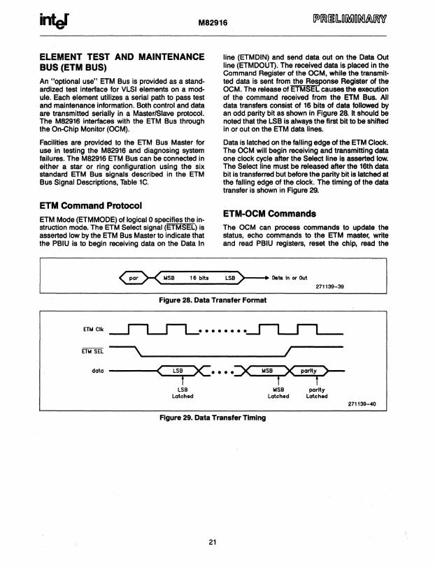
line (ETMDIN) and send data out on the Data Out line (ETMDOUT). The received data is placed in the Command Register of the OeM, while the transmitted data is sent from the Response Register of the OCM. The release of ETMSEL causes the execution of the command received from the ETM Bus. All data transfers consist of 16 bits of data followed by an odd parity bit as shown in Figure 28. It should be noted that the LSB is always the first bit to be shifted in or out on the ETM data lines.
Data is latched on the falling edge of the ETM Clock. The OCM will begin receiving and transmitting data one clock cycle after the Select line is asserted low. The Select line must be released after the 16th data bit is transferred but before the parity bit is latched at the falling edge of the clock. The timing of the data transfer is shown in Figure 29.
ETM-OCM Commands
The OCM can process commands to update the status, echo commands to the ETM master, write and read PBIU registers, reset the chip, read the
G><_M_S_B __ l_6_b_lt_S __ LS_BJ)-- Data In or Out 271139-39
Figure 28. Data Transfer Format
ETMClk~ •••••••• ~
~MSEL ~~ ________________________ --JI
data ------«~:JL~S~B;:::>C •••• y __ M_S_B..,..."X
LSB Latched
Figure 29. Data Transfer Timing
21
MSB Latched
parity >-f
parity Latched
271139-40
inter M82916
status, float all drivers, enable the Random Pattern Generator (RPG) and the Multiple Input Signature Register (MISR) and start, stop, and step PBIU clocks.
The ETM Write Register command can write to the Interrupt Enable Register and the PBIU Control Register (bits 0 through 7). The ETM Read Register Command can read from the PBIU Control Register, Local Bus Error Registers, and the Pi Bus Error Registers.
Chip Test Facilities
The PBIU has four chip test facilities available to the ETM Bus: signature analysis, boundary scan, scan string scan, and clock control. During signature analysis, the registers, counters, and other memory elements of the PBIU are configured into multiple shift registers or scan strings. Once an initial pattern of zeros is scanned into all scan strings, and the MISR and a seed into the RPG, the RPG will fill the scan strings with a random pattern. The PBIU is clocked once to pass the data through the combinational
22
logic of the chip. The scan strings are then scanned again to collect the signature in the MISR and to fill them with a new random pattern. This is repeated until the proper test coverage is reached. The signature in the MISR is then read by the ETM bus and compared to the correct value.
The second chip test facility is boundary scan. All of the storage elements, registers, etc., which directly control or monitor the chip input are configured into two boundary scan strings, one input string and one output string. This permits loading of the chip boundaries with known patterns, clocking them to other chips and scanning the other chip boundary scan strings and comparing the results.
The third chip test facility is scan string scanning. Each of the 23 scan strings of the PBIU can be individually scanned by the ETM bus. This permits access to all internal storage elements (registers, counters, etc.) for reading and writing.
The fourth chip test facility is clock control. The OCM provides the capability to stop, start, and step the PBIU clocks by use of the Event Command.
inter M82916
PIN DESCRIPTIONS
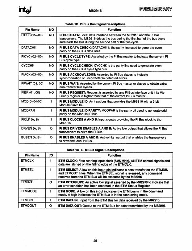
Table 1A. Local Bus Signal Descriptions
Pin Name 110 Function
LAB (21-16) 0 LOCAL ADDRESS BUS: The 22 local address bus lines output physical LAB (15-00) 110 memory addresses when the M82916 has control of the bus. Address lines
21-16 are output only. Addresses 15-0 are bi-directional and are used as inputs when the M82916 is being accessed by the host CPU. These lines are floated when the M82916 does not have control of the Local Bus. LAB21 is the Most Significant Bit (MSB), and LABOO is the Least Significant Bit (LSB).
LABPHI 0 ADDRESS PARITY: The address bus is parity protected and uses odd parity. LABPLO I/O The LABPHlline applies to address lines 21-16 and the MCMO (02-00) lines.
LABPLO applies to address lines 15-00. These lines are floated when the M82916 does not have control of the Local Bus.
LOB (31-00) 110 LOCAL DATA BUS: The local data bus supports 32-bit data transfers with an odd parity bit associated with each 16-bit word. Data bus lines 15-00 are the low word and are used during 16-bit transfers. Bits 31-16 constitute the high word. All 32 LOB lines are floated when the PBIU is not the Local Bus master. LOB31 is the MSB, and LOBOO is the LSB.
LOBPHI 110 DATA BUS PARITY: Odd parity is checked or generated during read or write LOBPLO 110 operations respectively. LOBPHI is used for LOB lines 31-16, and LOBPLO is
used for LOB lines 15-00. These lines are floated when the M82916 does not have control of the Local Bus.
MCMO (02-00) 0 MEMORY COMMAND BUS: The MCMO lines are used to determine type of memory accesses. A memory access can be a read or a write and it can be 16 or 32 bits wide. MCM002 is the MSB, and MCMOOO is the LSB.
The MCMO lines are included with LAB lines 21-16 for the parity line LABPHI. These lines are floated when the M82916 does not have control of the Local Bus.
BPCHK 110 BLOCK PROTECT CHECK: Indicates a Block Protect Check sequence has been initiated by the Local Bus Master. The M82916 will perform a Block Protect Check sequence under the following conditions: - First write operation following a reset. - First write operation following notification to the M82916 that the protect bits
have changed. - Before crossing a 4K memory address boundary. - During a Read-Modify-Write Sequence.
RU I REGISTER UPDATE OPERATION: A low on this input pin indicates that a Register Update cycle is beginning. This pin in used as a chip-select input to execute register accesses.
RUSUS 110 REGISTER UPDATE SUSPEND: The M82916 asserts a low on this pin during accesses of the Data Link Layer registers. While RUSUS is low, the register data is being synchronized between the LBCLK and Pi Bus clock. RUSUS going high indicates the Data Link Layer register data has been written or is available to be read.
RUSEL I REGISTER UPDATE ADDRESS SELECT: The address space used for Register Updates is selected with the RUSEL bit. With RUSEL pin tied high (Vcc), the register addresses are contained in the address space of 3100-31FF and B100-B1FF. With the RUSEL pin tied low (GNO), the register addresses are contained in the address space of 3000-30FF and BOOO-BOFF. This bit allows two PBIUs to be resident on the same bus and still be addressed individually.
23

M82916
Table 1A. Local Bus Signal Descriptions (Continued)
Pin Name I/O Function
TACK 1/0 TRANSFER ACKNOWLEDGE: 'f.l\CK is asserted by the addressed device and indicates a valid data transfer on the Local Bus. TACK must be low along with BUSGNT to give control of the Local Bus to the M82916 after Bus Request has gone low. This pin is an input and floated by the M82916 except during one clock cycle of a Register Update sequence.
BUSREQ 0 LOCAL BUS REQUEST: A low is asserted by the M82916 when an access of the Local Bus is requested. The M82916 releases control of the bus by de-asserting this signal.
BUSGNT I LOCAL BUS GRANT: A low on this input and the TACK input indicates access of the Local Bus has been granted to the M82916. This input must remain low until BUSREQ is released.
APE I ADDRESS PARITY ERROR: APE is an active low input indicating an error on the Local Address Bus has occurred during memory operations for which the MCMO field is not a NOP.
OPE I/O DATA PARITY ERROR: A low input on this pin indicates that a parity error has been detected during a memory operation. A low output on this pin indicates that a parity error existed during a register update operation. This signal is otherwise floated by the M82916.
CHERR 0 I/O CHANNEL ERROR: Signal which is used to indicate an illegal Register Update or reserved Register Update operation. The M82916 will drive this output low when an invalid register address is detected during an RU operation.
MAE I MEMORY ACCESS ERROR: Active low input indicating an access to unimplemented memory.
LBCLK I LOCAL BUS CLOCK: Free running input clock used for all Local Bus timing. Inputs are latched in on the rising edge of the clock. Outputs are clocked out by the rising edge of this clock.
INT1 0 INTERRUPT 1: A level 1 interrupt is indicated to the host CPU when this pin is driven to a low level. The M82916 will halt Pi Bus operations when a level 1 interrupt occurs.
When in the interrupt pulse mode, a low pulse on the INT1 pin indicates that the current Pi Bus message ended with an error. This occurs during Slave Mode only.
INT2 0 INTERRUPT 2: A level 2 interrupt is indicated to the host CPU when this pin is driven to a low level. Pi Bus operation will continue when the M82916 generates a level 2 interrupt.
When in the interrupt pulse mode, a low pulse on the INT2 pin indicates that the current Pi Bus message ended successfully. This occurs during Slave Mode only.
TMRCLK I TIMER CLOCK: An input for the internal 32-bit System Timer. The System Timer is incremented by a high to low transition of the TMRCLK signal. TMRCLK is expected to be 1 MHz.
PRCHLT I PROCESSOR HALT: Active low input indicates that the host processor has been halted. It is used to halt the incrementing of the System Timer.
RST I SYSTEM RESET: A low on this pin for 10 LBCLK cycles will reset the M82916.
OEVBUSY I DEVICE BUSY: An active high signal which is asserted by the host to indicate that it is busy and cannot respond to accesses by the M82916. OEVBUSY is valid only when the PBIU Control register specifies "Pulsed Interrupt" mode.
24
M82916
Table 1 B PI Bus Bus Signal Descriptions
Pin Name 1/0 Function
PIBUS (15-00) 1/0 PI BUS DATA: Local data interface between the MB2916 and the Pi Bus transceivers. The M82916 drives the bus during the first half of the bus cycle and reads the bus during the second half of the bus cycle.
OATACHK 1/0 Pi BUS DATA CHECK: OATACHK is the parity line used to generate even parity on the Pi Bus data lines.
PICYC (02-00) 1/0 Pi BUS CYCLE TYPE: Asserted by the Pi Bus master to indicate the current Pi Bus cycle type.
CYCCHK 1/0 Pi BUS CYCLE CHECK: CYCCHK is the parity line used to generate even parity on the Pi Bus cycle type bus.
PlACK (03-00) 1/0 Pi BUS ACKNOWLEDGE: Asserted by Pi Bus slaves to indicate synchronization or uncorrectable detected errors.
PIWAIT (01,00) 1/0 Pi BUS WAIT: Asserted by the current Pi Bus master or slaves to obtain extra non-transfer bus cycles.
PIBR (01, 00) 1/0 Pi BUS REQUEST: Request is asserted by any Pi Bus interface unit if its Vie Priority register is higher than that of the current Pi Bus master.
MOOIO (04-00) I Pi BUS MODULE 10: An input bus that provides the M82916 with a 5-bit Module Slave 10.
MOOPAR I Pi BUS MODULE 10 PARITY: MOOPAR is the parity bit used to generate odd parity on the Module 10 bus.
PICLK (A, B) I PI BUS CLOCKS A AND B: Input signals providing the Pi Bus clock to the M82916.
ORVEN (A, B) 0 Pi BUS DRIVER ENABLES A AND B: Active low output that allows the Pi Bus transceivers to drive the Pi Bus.
BUSEN (A, B) 0 Pi BUS ENABLES A AND B: Active high output that enables the transceivers to drive the local Pi Bus.
Table 1C. ETM Bus Signal Descriptions
Pin Name 110 Function
ETMCLk I ETM CLOCK: Free running input clock (6.25 MHz). All ETM control signals and data are latched on the falling edge of the ETMCLK.
ETMSEL I ETM SELECT: A low on this inl'ut pin indicates a data transfer on the ETMDIN and ETMOUT lines. When the ETMSEL signal is released, any command received from the ETM Bus will be executed by the M82916.
ETMINT 0 ETM INTERRUPT: An active low signal asserted by the M82916 to indicate that an error condition has been recorded in the ETM Status Register.
ETMMOOE I ETM MODE: A low on this input indicates the ETM bus is in the command mode. A high indicates the ETM Bus is in the scan string mode.
ETMOIN I ETM DATA IN: Input from the ETM Bus for data received by the M82916.
ETMDOUT 0 ETM DATA OUT: Output to the ETM Bus for data transmitted by the M82916.
25
inter M82916
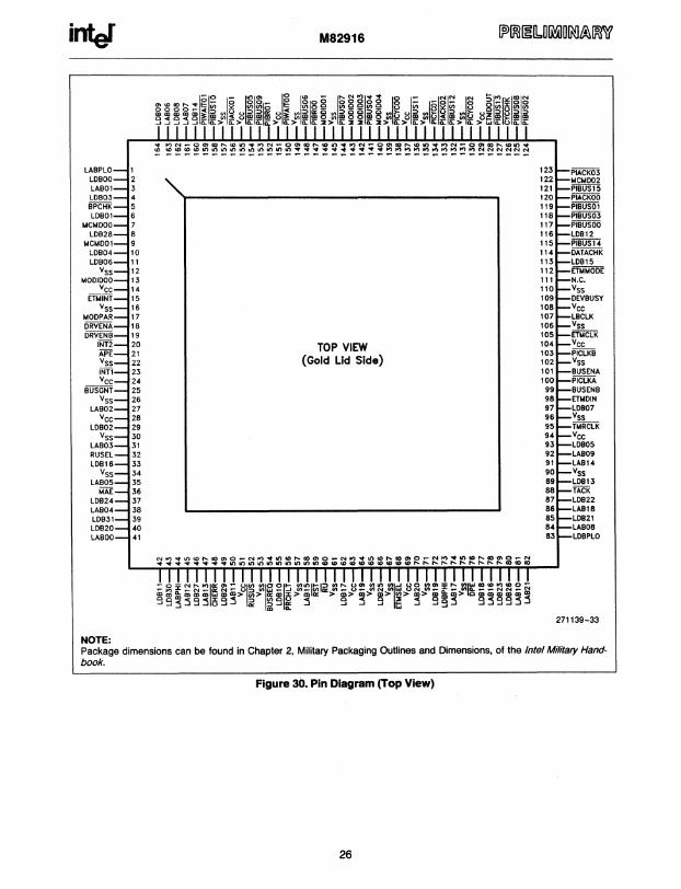
LABPLO 1 123 PIACK03 LOBOO 2 122 MCMOO2 LABOI 3 121 PIBUS15 LOB03 4 120 PIACKOO BPCHK 5 119 PIBUSOI LOBOI 6 118 PIBUS03
MCMOOO 7 117 PIBUSOO LOB28 8 116 LOB12
MCMOOI 9 115 PIBUS14 LOB04 10 114 OATACHK LOB06 11 113 LOB15
VSS 12 112 ETMMOOE MODlOOO 13 111 N.C.
Vee 14 110 VSS ETMINT 15 109 OEVBUSY
VSS 16 108 Vee MOOPAR 17 107 LBCLK ORVENA 18 106 Vss
ORVENB 19 105 ETMCLK INT2 20 TOP VIEW 104 Vee
APE 21 103 PICLKB VSS 22 (Gold Lid Side) 102 Vss
INTI 23 101 BUSENA Vee 24 100 PICLKA
BUSGNT 25 99 BUSENB
Vss 26 98 ETMOIN LAB02 27 97 LOB07
Vee 28 96 Vss
LOB02 29 95 TMRCLK
Vss 30 94 VCC LAB03 31 93 LOB05
RUSEL 32 92 LAB09
LOB16 33 91 LAB14
Vss 34 90 Vss LAB05 35 89 LOB13
MAE 36 88 TACK
LOB24 37 87 LOB22
LAB04 38 86 LAB18
LOB31 39 85 LOB21 LOB20 40 84 LAB08
LABOO 41 83 LOBPLO
271139-33
NOTE: Package dimensions can be found in Chapter 2, Military Packaging Outlines and Dimensions, of the Intel Military Handbook.
Figure 30. Pin Diagram (Top View)
26

inlef M82916
PlACK03 123 LABPLO MCMOO2 122 L0800 PIBUS1S 121 LABDI PIACKDD 120 LOBD3 PIBUSDI 119 BPCHK PIBUSD3 118 LOBDI PIBUSOO 117 MCMOOD
LOB12 116 LOB28 PIBUS14 115 MCMOOI OATACHK 114 L0B04
LDB1S 113 OBD6 ETMMODE 112 SS
N.C. 111 MODIOOD VSS 110 Vee
OEVBUSY 109 ETMINT Vee 108 Vss
LBCLK 107 MODPAR
~ 106 DRVENA ETMCLK 105 DRVENB
Vee 104 BOTTOM SIDE INT2 PICLKB 103 APE
Vss 102 VIEW Vss BUSENA 101 INTI PICLKA 100 Vee
BUSENB 99 BUSGNT ETMOIN 98 Vss LOB07 97 LABD2
Vss 96 Vee TMRCLK 95 LOBD2
Vee 94 Vss LOBDS 93 LAB03 WD9 92 RUSEL LAB14 91 LOB16
Vss 90 Vss LDB13 89 LABOS
TACK 88 MAE LOB22 87 LDB24 LAB1S 86 LABD4 LOB21 85 LDB31
LABOS 84 LOB2D LOBPLD 83 LABOO
271139-34
NOTE: Package dimensions can be found in Chapter 2, Military Packaging Outlines and Dimensions. of the Intel Military Handbook.
Figure 31. Pin Diagram (Bottom Side View)
27
inter M82916
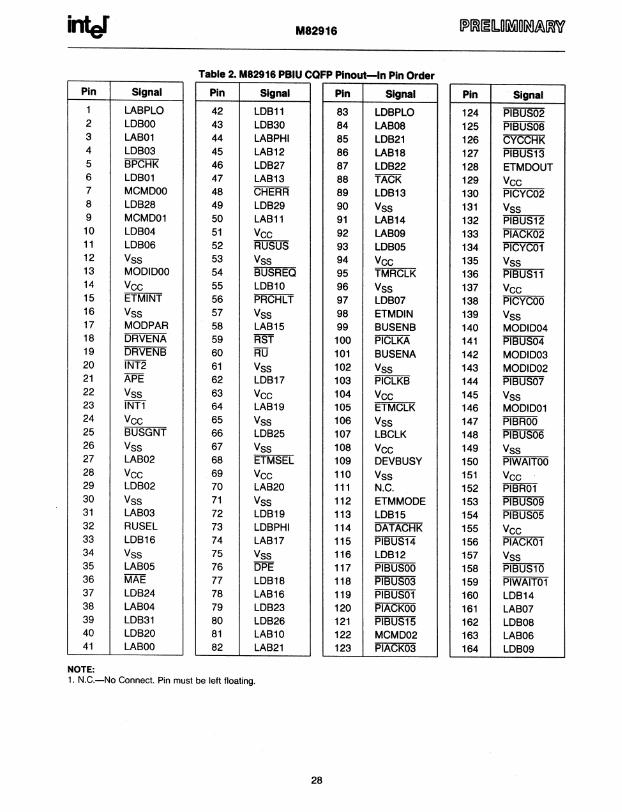
Table 2. M82916 PBIU CQFP Plnout-ln Pin Order
Pin Signal Pin Signal Pin Signal Pin Signal
1 LABPLO 42 LDB11 83 LDBPLO 124 PIBUS02 2 LDBOO 43 LDB30 84 LAB08 125 PI BUS08 3 LAB01 44 LABPHI 85 LDB21 126 CYCCHK 4 LDB03 45 LAB12 86 LAB18 127 PIBUS13 5 BPCHK 46 LDB27 87 LDB22 128 ETMDOUT 6 LDB01 47 LAB13 88 TACK 129 Vcc 7 MCMDOO 48 CHERR 89 LDB13 130 PICYC02 8 LDB28 49 LDB29 90 VSS 131 VSS 9 MCMD01 50 LAB11 91 LAB14 132 PIBUS12 10 LDB04 51 Vee 92 LAB09 133 PIACK02 11 LDB06 52 RUSUS 93 LDB05 134 PICYC01 12 VSS 53 VSS 94 Vcc 135 Vss 13 MODIDOO 54 BUSREO 95 TMRCLK 136 PIBUS11 14 Vee 55 LDB10 96 VSS 137 Vee 15 ETMINT 56 PRCHLT 97 LDB07 138 PICYCOO 16 VSS 57 VSS 98 ETMDIN 139 VSS 17 MODPAR 58 LAB15 99 BUSENB 140 MODID04 18 DRVENA 59 RST 100 PICLKA 141 PIBUS04 19 DRVENB 60 RU 101 BUSENA 142 MODlD03 20 INT2 61 Vss 102 VSS 143 MODID02 21 APE 62 LDB17 103 PICLKB 144 PIBUS07 22 VSS 23 INT1
63 Vcc 64 LAB19
104 Vee 105 ETMCLK
145 VSS 146 MODID01
24 VCC 65 VSS 106 VSS 147 PIBROO 25 BUSGNT 66 LDB25 107 LBCLK 148 PIBUS06 26 VSS 67 VSS 108 Vee 149 VSS 27 LAB02 68 ETMSEL 109 DEVBUSY 150 PIWAITOO 28 VCC 69 Vcc 110 Vss 151 Vcc 29 LDB02 70 LAB20 111 N.C. 152 PIBR01 30 VSS 71 VSS 112 ETMMODE 153 PIBUS09 31 LAB03 72 LDB19 113 LDB15 154 PIBUS05 32 RUSEL 73 LDBPHI 114 DATACHK 155 Vcc 33 LDB16 74 LAB 17 115 PIBUS14 156 PIACK01 34 VSS 75 VSS 116 LDB12 157 VSS 35 LAB05 76 DPE 117 PIBUSOO 158 PIBUS10 36 MAE 77 LDB18 118 PIBUS03 159 PIWAIT01 37 LDB24 78 LAB16 119 PIBUS01 160 LDB14 38 LAB04 79 LDB23 120 PIACKOO 161 LAB07 39 LDB31 80 LDB26 121 PIBUS15 162 LDB08 40 LDB20 81 LAB10 122 MCMD02 163 LAB06 41 LABOO 82 LAB21 123 PIACK03 164 LDB09
NOTE: 1. N.C.-No Connect. Pin must be left floating.
28

inter M82916
Table 3. M82916 PBIU CQFP Pinout-In Signal Order
Signal Pin Signal Pin Signal Pin Signal Pin
LAB21 82 LDB31 39 PIBUS15 121 INT1 23
LAB20 70 LDB30 43 PIBUS14 115 INT2 20
LAB19 64 LAB18 86 LAB 17 74 LAB16 78
LDB29 49 LDB28 8 LDB27 46 LDB26 80
PIBUS13 127 PIBUS12 132 PIBUS11 136 PIBUS10 158 PIBUS09 153
TMRCLK 95 PRCHLT 56 RST 59 DEVBUSY 109
LAB15 58 LAB14 91 LAB13 47 LAB12 45 LAB11 50 LAB10 81 LAB09 92 LAB08 84 LAB07 161 LAB06 163
LDB25 66 LDB24 37 LDB23 79 LDB22 87 LDB21 85 LDB20 40 LDB19 72 LDB18 77 LDB17 62 LDB16 33
PIBUS08 125 PIBUS07 144 PIBUS06 148 PIBUS05 154 PIBUS04 141 PIBUS03 118 PIBUS02 124 PIBUS01 119 PIBUSOO 117 DATACHK 114
Vee 14 Vee 24
Vec 28
Vee 51
Vec 63
Vee 69
Vec 94
Vee 104
Vee 108 Vee 129
LAB05 35 LDB15 113 PICYC02 130 Vec 137
LAB04 38 LDB14 160 PICYC01 134 Vee 151
LAB03 31 LDB13 89 PICYCOO 138 Vee 155
lAB02 27 LDB12 116 CYCCHK 126
LAB01 3 LABOO 41 LABPHI 44 LABPLO 1
LDB11 42 LDB10 55 LDB09 164 LDB08 162 LDB07 97
PIACK03 123 PIACK02 133 PIACK01 156 PIACKOO 120
Vss 12 Vss 16
Vss 22
Vss 26
Vss 30
MCMD02 122 MCMD01 9
LDB06 11 LDB05 93 LDB04 10
PIBR01 152 ~ 147
Vss 34
Vss 53 Vss 57
MCMDOO 7
BPCHK 5 RU 60 RUSUS 52 RUSEL 32 TACK 88 BUSREQ 54 BUSGNT 25
LDB03 4 LDB02 29 LDB01 6 LDBOO 2 LDBPHI 73 LDBPLO 83
ETMCLK 105 ETMSEL 68
PIWAIT01 159 PIWAITOO 150
MODID04 140 MODID03 142 MODID02 143 MODID01 146 MODIDOO 13 MOD PAR 17
Vss 61
Vss 65
Vss 67
Vss 71
Vss 75
Vss 90
Vss 96
Vss 102
Vss 106
Vss 110
APE 21 ETMINT 15 ETMMODE 112
PICLKA 100 PICLKB 103
Vss 131
Vss 135 DPE 76 ETMDIN 98 DRVENA 18 Vss 139 MAE 36 ETMDOUT 128 DRVENB 19 Vss 145 CHERR 48 BUSENA 101 Vss 149
LBCLK 107 N.C. 111 BUSENB 99 Vss 157
NOTE: 1. N.C.-No Connect. Pin must be left floating.
29
M82916
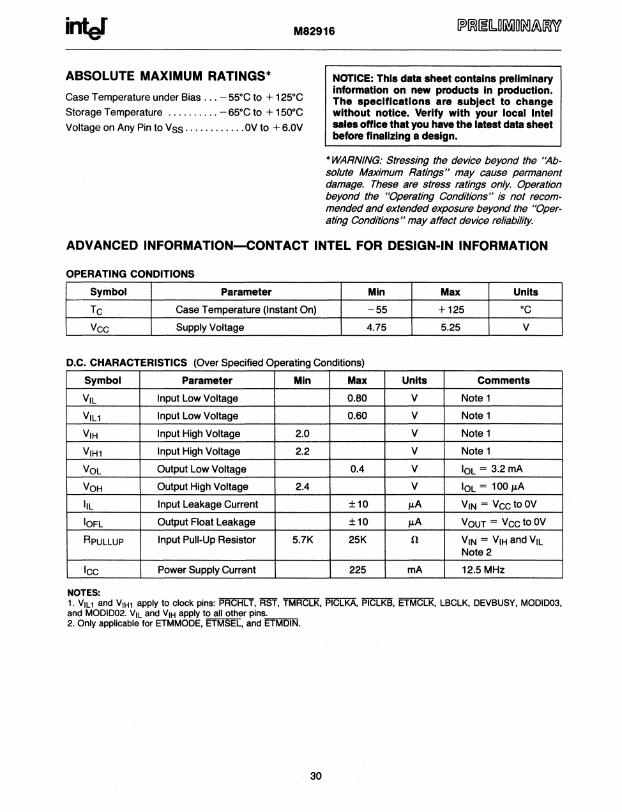
ABSOLUTE MAXIMUM RATINGS*
Case Temperature under Bias ... - 55°C to + 125°C
Storage Temperature .......... - 65°C to + 150°C
Voltage on Any Pin to Vss ............ OV to + 6.0V
NOTICE: This data sheet contains preliminary Information on new products in production. The specifications are subject to change without notice. Verify with your local Intel sales office that you have the latest data sheet before finalizing a design.
• WARNING: Stressing the device beyond the 'i4bsolute Maximum Ratings" may cause permanent damage. These are stress ratings only. Operation beyond the "Operating Conditions" is not recommended and extended exposure beyond the "Operating Conditions" may affect device reliability.
ADVANCED INFORMATION-CONTACT INTEL FOR DESIGN-IN INFORMATION
OPERATING CONDITIONS
Symbol Parameter Min Max Units
Tc Case Temperature (Instant On) -55 +125 °C
Vcc Supply Voltage 4.75 5.25 V
D.C. CHARACTERISTICS (Over Specified Operating Conditions)
Symbol Parameter Min Max Units Comments
VIL Input Low Voltage 0.80 V Note 1
VIL1 Input Low Voltage 0.60 V Note 1
VIH Input High Voltage 2.0 V Note 1
VIH1 Input High Voltage 2.2 V Note 1
VOL Output Low Voltage 0.4 V IOL = 3.2mA
VOH Output High Voltage 2.4 V IOL = 100 p,A
IlL Input Leakage Current ±10 p,A VIN = Vcc to OV
IOFL Output Float Leakage ±10 p,A VOUT = Vcc to OV
RpULLUP Input Pull-Up Resistor 5.7K 25K n VIN = VIH and VIL Note 2
Icc Power Supply Current 225 mA 12.5 MHz
NOTES: 1. VIL1 and VIH1 apply to clock pins: PRCHLT, RS'f, TMRCLK, PICLKA, PICLKB, ETMCLK, LBCLK, DEVBUSY, MODID03, and MODID02. VIL and VIH apply to all other pins. 2. Only applicable for ETMMODE, ETMSEL, and ETMDIN.
30

M82916
A.C. SPECIFICATION TABLES (Over Specified Operating Conditions)
LBCLK INPUT TIMINGS
Symbol Parameter Min Max Units Fig. Comments
LBCLK Frequency 12.5 MHz 32
Tl LBCLK Period 80 ns 32
T2 LBCLK High Time 30 ns 32
T3 LBCLK Low Time 30 ns 32
T4 LBCLK Fall Time 5 ns 32
T5 LBCLK Rise Time 5 ns 32
LBCLK to PICLK Frequency Ratio 0.25 1 -
DMA OUTPUT TIMINGS
Symbol Parameter Min Max Units Fig. Comments
T6 LBCLK Rise to BUSREQ Valid 26 ns 33
T7 BUSGNT Fall to LAB Valid 41 ns 33
Ts BUSGNT Rise to LAB Float 24 ns 33
T9 LBCLK Rise to LAB Valid 58 ns 33
TlO LBCLK Rise to LAB Float 46 ns 33
Tll BUSGNT Fall to MCMO Active 41 ns 33
T12 BUSGNT Rise to MCMO Float 24 ns 33
T13 LBCLK Rise to MCMO Valid 54 ns 33
T14 LBCLK Rise to MCMO Float 46 ns 33
T15A LBCLK Rise to LOB Valid 47 ns 33 First Data Word
T15B LBCLK Rise to LOB Valid 38 ns 33 Next Data Word
T16 LBCLK Rise to LOB Float 22 ns 33
INPUT TIMINGS
Symbol Parameter Min Max Units Fig. Comments
T17 BUSGNT Setup to LBCLK Rise 15 ns 33
T1S BUSGNT Hold after LBCLK Rise 12 ns 33
T19 LAB, LOB Setup to LBCLK Rise 12 ns 34
T20 LAB, LOB Hold after LBCLK Rise 13 ns 35
T21 Error Setup to LBCLK Rise 12 ns 33, 35 Note 3
T22 Error Hold after LBCLK Rise 11 ns 33, 35 Note 3
T23 RU Setup to LBCL!< Rise 11 ns 34
T24 RU Hold after LBCLK Rise 7 ns 34
T25 RU Low Width 1 Tl 34
NOTE: 3. Error signals include: APE, MAE, DPE, and BPCHK.
31
M82916
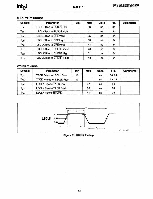
RU OUTPUT TIMINGS
Symbol Parameter Min
T26 LBCLK Rise to RUSUS Low
T27 LBCLK Rise to RUSUS High
T28 LBCLK Rise to OPE Valid
T29 LBCLK Rise to OPE High
T30 LBCLK Rise to OPE Float
T31 LBCLK Rise to CHERR Valid
T32 LBCLK Rise to CHERR High
T33 LBCLK Rise to CHERR Float
OTHER TIMINGS
Symbol Parameter Min
T34 TACK Setup to LBCLK Rise 13
T35 TACK Hold after LBCLK Rise 10
T36 LBCLK Rise to TACK Low
T37 LBCLK Rise to TACK Float
T38 LBCLK Rise to BPCHK
2.2V--.w:----~
LBCLK 1.5V
O.6V
Max
56
41
65
53
44
46
31
43
Max
47
33
41
Figure 32. LBCLK Timings
32
Units Fig. Comments
ns 34
ns 34
ns 34
ns 34
ns 34
ns 34
ns 34
ns 34
Units Fig. Comments
ns 33,34
ns 33,34
ns 34
ns 34
ns 35
271139-38
inter M82916
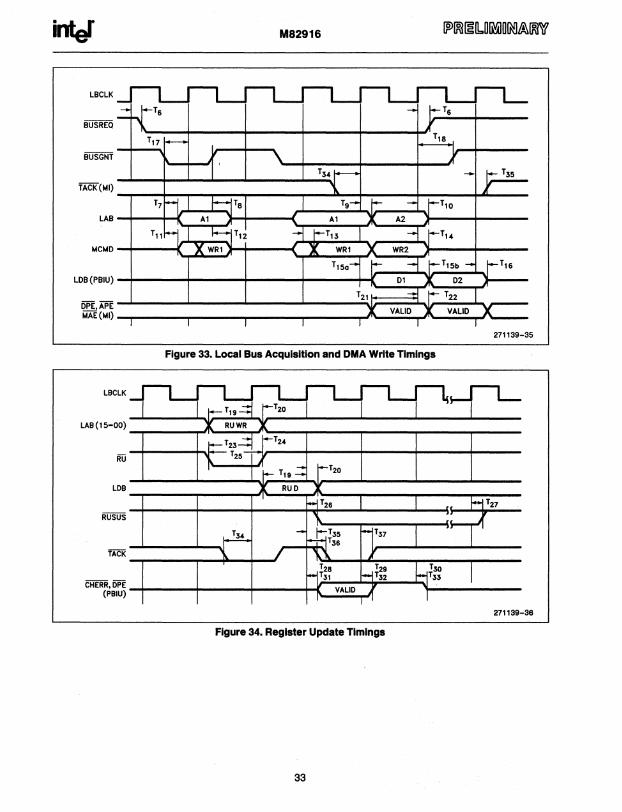
LBCLK
TACK (MI) ~---+~~~~~----~--~-+~--~~----~----
LOB (PBIU) -r---+----t----1--....:.:::..t-t~~:x:::§:~j---oPE.APE-L----J-----L---~----~~~~~~-2~-1~J---MAE (MI) -T"'""---"T""'---..,..---....,----..,..,"-....;.;.;;;;.;;...,..."'".....;,~;;..,.J .... ---
271139-35
Figure 33. Local Bus Acquisition and DMA Write Timings
LBCLK
LAB (1 S-OO) -r-----,....n---~'---.,_---"T""'---..,..---..,..---
CHERR.DPE--r---~----t----t-K~~~:t~-~~~--~----(PBIU)
271139-36
Figure 34. Register Update Timings
33
inter M82916
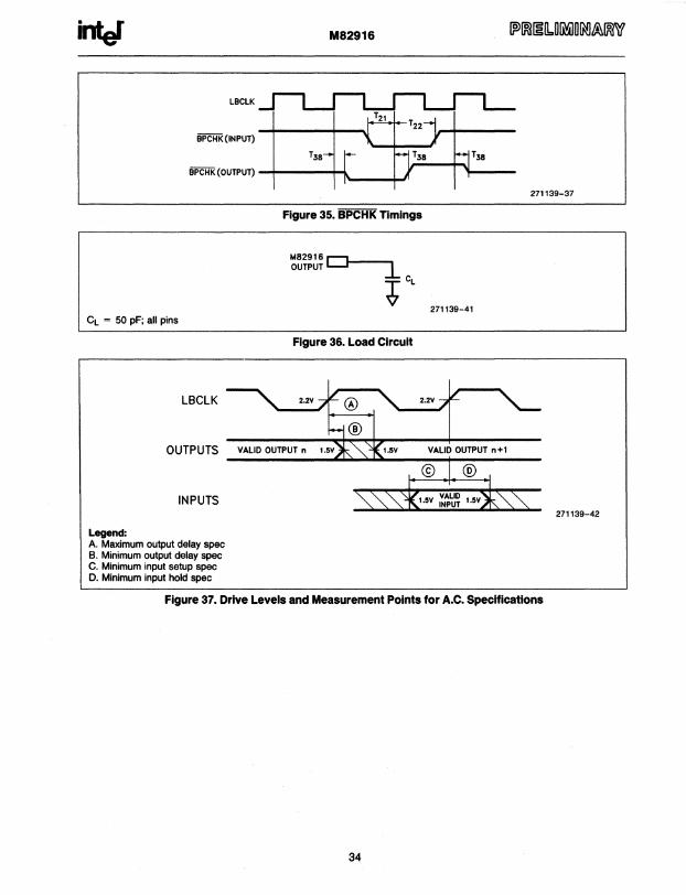
LBCLK
BPCHK (iNPUT)
BPCHK (OUTPUT) -i---it-... __ -I-)..;.;.--t-i":':_-
CL = 50 pF; all pins
LBCLK
OUTPUTS
INPUTS
Legend: A. Maximum output delay spec B. Minimum output delay spec C. Minimum input setup spec D. Minimum input hold spec
Figure 35. BPCHK Timings
M82916 c::J---, OUTPUT - ..L
~CL
Figure 36. Load Circuit
271139-41
271139-37
271139-42
Figure 37. Drive Levels and Measurement Points for A.C. Specifications
34

I
inter ALABAMA
tlntal Corp. 5015 Bradford Or .• #2 Huntsville 35805 Tet: (205) 830-4010 FAX: (205) 837-2640
ARIZONA
tlntal Corp. 410 North 44th Street Suite 500 Phoenix 85008 Tet: (602) 231-0386 FAX: (602) 244-0446
Intel Corp. 7225 N. Mona Usa Rd. Suite 215 Tucson 85741 Tet: (602) 544-0227 FAX: (602) 544-0232
CALIFORNIA
tlntel Corp. 21515 Vanowen Street Suite 116 Canoga Park 91303 Tel: (818) 704-8500 FAX: (818) 340-1144
tlntel Corp. 2250 E. Imperial Highway Suite 218
i~I~(~~~)d~~~ FAX: (213) 640-7133
Intel Corp. 1 Sierra Gate Plaza Suite 280C Roseville 95678 Tel: (916) 782-8086 FAX: (916) 782-8153
tlntel Corp. 9665 Chesapeake Dr. Suite 325 San Diego 92123 Tel: (619) 292-8086 FAX: (619) 292-0628
tlntel Corp." 400 N. Tustin Avenue Suite 450 Santa Ana 92705 Tel: (714) 835-9642 TWX: 910-595-1114 FAX: (714) 541-9157
tlntel Corp. * San Tomas 4 2700 San Tomas Expressway 2nd Floor Santa Clara 95051 Tel: (408) 986-8086 TWX: 910-338-0255 FAX: (408) 727-2620
CDLORAOO
Intel Corp. 4445 Northpark Drive Suite 100 Colorado Springs 80907 Tel: (719) 594-6622 FAX: (303) 594-0720
tlntel Corp. * 650 S. Cherry SI. Suite 915 Denver 80222 Tel: (303) 321-8086 TWX: 910-931-2289 FAX: (303) 322-8670
CONNECTICUT
Intel Corp. 301 Lee Farm Corporate Park 83 Wooster Heights Rd. Danbury 06810 Tel: (203) 748-3130 FAX: (203) 794-0339
tSales and Service Office 10Field Application location
DOMESTIC SALES OFFICES FLORIOA MICHIGAN tlntal Corp.· VIRGINIA
tlnlal COrp. 25700 Science Park Dr.
tlnlal Corp. Suite 100 tlnlal Corp. 800 Fairway Drive 7071 Orchard Lake Road Beachwood 44 122 1504 santa Rosa Road Suite 160 Suite 100 Tel: (216) 464-2736 Suite 108 Deerfield Beach 33441 West Bloomfield 48322 1WX: 810-427-9298 Richmond 23288 Tel: (305) 421-0506 Tel: (313) 851-8096 FAX: (804) 282-0673 Tel: (804) 282-5668 FAX: (305) 421-2444 FAX: (313) 851-8770 FAX: (216) 464-2270
tlntel Corp. MINNESOTA OKLAHOMA 5850 T.G. Lee Blvd. WASHINGTON Suite 340 tlnlal Corp. Intel Corp. Orlando 32822 3500 W. 80th St. 6801 N. BrOadway tlntal Corp. Tel: (407) 240-8000 Suite 360 Suite 115 155 1000h Avenue N.E. FAX: (407) 240-8097 ~~~n2r:5~~~~ Oklahoma City 73162 Suite 386
Tel: (405) 648-8086 Bellevue 98004 Intel Corp. TWX: 910-576·2867 FAX: (405) 840-9819 Tel: (206) 453-8080 11300 4th Street North FAX: (612) 831-6497 TWX: 910-443-3002 Suite 170
MISSOURI OREGON FAX: (206) 451-9556
St. Petersburg 33716 Tel: (813) 577-2413 tlntel Corp. tlntei Corp. ~nJ:1 ~°.:rUlian Road FAX: (813) 578-1607 4203 Earth City Expressway 15254 N. W. Greenbrier Parkway Suite 102 Suite 131 Building B Spokane 99206 GEORGIA i:r~3~~ ~~90 Beaverton 97005 Tet: (509) 928-8086
Tel: (503) 645-8051 FAX: (509) 928-9467 tlntel Corp. FAX: (314) 291-4341 TWX: 910-467·8741 20 Technology Parkway FAX: (503) 645-8181 Suite 150 NEW JERSEY WISCONSIN Norcross 30092
tlntel Corp." Tel: (404) 449-0541 PENNSYLVANIA Intel Corp. FAX: (404) 605-9762 Parkway 1 09 Office Center
330 S. Executive Or. 328 Newman Springs Road tlntel Corp." Suite 102 Red Bank 07701 925 Harvest Drive Brookfield 53005 ILLINOIS Tel: (201) 747-2233 Suite 200 Tel: (414) 784-8087 tlntel Corp."
FAX: (201) 747-0983 Blue Bell 19422 FAX: (414) 796-2115 Woodfietd Corp. Center III Intel Corp. Tel: (215) 641·1000 300 N. Martingale Road 280 Corporate Center FAX: (215) 641-0785 Suite 400 75 Uvingston Avenue
tlntel Corp." CANADA SChaumburg 60173 First Floor Tel: (708) 605-8031 Roseland 07068 400 Penn Center Blvd. FAX: (708) 706-9762 Tel: (201) 740-0111 Suite 610
FAX: (201) 740-0626 Pittsburgh 15235 BRITISH COLUMBIA Tel: (412) 823-4970
Intel Semiconductor of INDIANA NEW YORK FAX: (412) 829-7578 Canada. ltd.
Intel Corp. Intel Corp." PUERTO RICO
4585 Canada Way 8910 Purdue Road 850 Crosskeys Office Park Suite 202 Suite 350 Fairport 14450 Burnaby V5G 4L6 Indianapolis 46268 Tet: (716) 425-2750 tlntel Corp. Tel: (604) 298-0367 Tel: (317) 875-0623 TWX: 510-253-7391 South Industrial Park FAX: (804) 298-8234 FAX: 1317) 875-8938 FAX: (716) 223-2561 P.O. Box 910
Las Piedras 00671 tlntel Corp. * Tel: (809) 733-8616 ONTARIO
IOWA 2950 Express Dr .. South Suite 130 tlntel Semiconductor of
Intel Corp. Islandia 11722 TEXAS Canada. Ltd. 1930 St. Andrews Drive N.E. Tel: (516) 231-3300 2650 Oueensview Drive 2nd Floor 1WX: 510-227-6236 Intel Corp. Suite 250 Cedar Rapids 52402 FAX: (516) 348-7939 8911 Capital of Texas Hwy. Ottawa K2B 8H6 Tel: (319) 393·5510 Austin 78759 rel: (613) 829-9714
~~,:~~~r~~siness Center Tel: (512) 794-8086 FAX: (613) 820-5936
KANSAS FAX: (512) 338-9335 Bldg. 300. Route 9 tlntel Semiconductor of
tlntel Corp. Fishkill 12524 tlntel Corp. * Canada. Ltd. Tet: (914) 897-3860 12000 Ford Road 190 Attwell Drive 10985 Cody SI. FAX: (914) 897-3125 Suite 400 Suite 500 Suite 140 Overland Park 66210 DaUas 75248 Rexdale M9W 6H8 Tel: (913) 345-2727 NORTH CAROUNA Tel: (214) 241-8087 Tel: (416) 675-2105 FAX: (913) 345-2076 tlntel Corp.
FAX: (214) 484-1180 FAX: (416) 675-2438
5800 Executive Center Dr. tlntel Corp. * MARYLAND Suite 105 QUEBEC
Charlotte 28212 7322 S.W. Freeway Suite 1490
tlntel Corp." Tel: (704) 568-8966 Houston 77074 tlntef Semiconductor of 10010 Junction Or. FAX: (704) 535-2236 Tel: (713) 988-8086 Canada. Ltd. Suite 200
tlntel Corp. TWX: 910-881·2490 1 Rue Holiday Annapolis Junction 20701 FAX: (713) 988-3660 Suite 115 Tel: (301) 206-2860 5540 Centerview Dr.
Tour East FAX: (301) 206-3677 Suite 215
Pt. Claire H9R 5N3 (301) 206-3678 Raleigh 27606
UTAH Tel: (514) 694-9130 Tel: (919) 851-9537 FAX: 514-694-0064 FAX: (919) 851-8974 tlntel Corp. MASSACHUSETTS
428 East 6400 South
tlntel Corp." OHIO Suite 104
Westford Corp. Center tlntel Corp." Murray 84107
3 Carlisle Road 3401 Park Center Drive Tel: (801) 263-8051
2nd Floor Suite 220 FAX: (801) 268-1457
Westford 01886 Dayton 45414 Tel: (508) 692-0960 Tel: (513) 890-5350 TWX: 710-343-6333 TWX: 810-450-2528 FAX: (508) 692-7867 FAX: (513) 890-8658
CG/SALE/081090
UNITED STATES, Intel Corporation 3065 Bowers Ave., Santa Clara, CA 95051
Tel: (408) 765-8080
JAPAN, Intel Japan K.K. 5-6 Tokodai, Tsukuba-shi, Ibaraki, 300-26
Tel: 0298-47-8511
FRANCE, Intel Corporation S.A.R.L. 1, Rue Edison, BP 303, 78054 Saint-Quentin-en-Yvelines Cedex
Tel: (33) (1) 30 57 70 00
UNITED KINGDOM, Intel Corporation (UK) Ltd. Pipers Way, Swindon, Wiltshire, England SN3 1 RJ
Tel: (44) (0793) 696000
WEST GERMANY, Intel GmbH Dornacher Strasse 1
8016 Feldkirchen bei Muenchen Tel: (49) 089/90992-0
HONG KONG, Intel Semiconductor Ltd. 10/F East Tower, Bond Center, Queensway, Central
Tel: (852) 844-4555
CANADA, Intel Semiconductor of Canada, Ltd. 190 Attwell Drive, Suite 500 Rexdale, Ontario M9W 6H8
Tel: (416) 675-2105
Printed in U.S.A.lM346J0990/3K1HP OM CG/081090
Related Documents