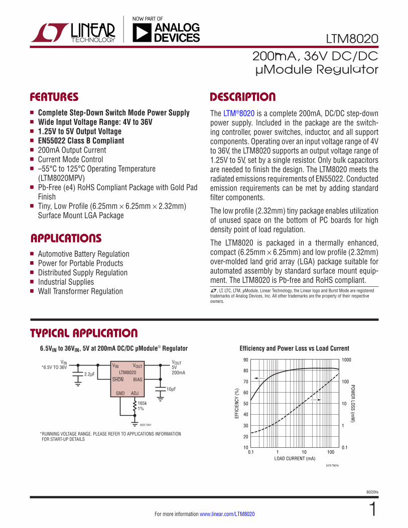
LTM8020 1 8020fe For more information www.linear.com/LTM8020 TYPICAL APPLICATION FEATURES APPLICATIONS DESCRIPTION 200mA, 36V DC/DC µModule Regulator The LTM ® 8020 is a complete 200mA, DC/DC step-down power supply. Included in the package are the switch- ing controller, power switches, inductor, and all support components. Operating over an input voltage range of 4V to 36V, the LTM8020 supports an output voltage range of 1.25V to 5V, set by a single resistor. Only bulk capacitors are needed to finish the design. The LTM8020 meets the radiated emissions requirements of EN55022. Conducted emission requirements can be met by adding standard filter components. The low profile (2.32mm) tiny package enables utilization of unused space on the bottom of PC boards for high density point of load regulation. The LTM8020 is packaged in a thermally enhanced, compact (6.25mm × 6.25mm) and low profile (2.32mm) over-molded land grid array (LGA) package suitable for automated assembly by standard surface mount equip- ment. The LTM8020 is Pb-free and RoHS compliant. L, LT, LTC, LTM, µModule, Linear Technology, the Linear logo and Burst Mode are registered trademarks of Analog Devices, Inc. All other trademarks are the property of their respective owners. Efficiency and Power Loss vs Load Current n Complete Step-Down Switch Mode Power Supply n Wide Input Voltage Range: 4V to 36V n 1.25V to 5V Output Voltage n EN55022 Class B Compliant n 200mA Output Current n Current Mode Control n –55°C to 125°C Operating Temperature (LTM8020MPV) n Pb-Free (e4) RoHS Compliant Package with Gold Pad Finish n Tiny, Low Profile (6.25mm × 6.25mm × 2.32mm) Surface Mount LGA Package n Automotive Battery Regulation n Power for Portable Products n Distributed Supply Regulation n Industrial Supplies n Wall Transformer Regulation 6.5V IN to 36V IN , 5V at 200mA DC/DC µModule ® Regulator V IN V OUT LTM8020 BIAS SHDN 10μF 165k 1% 2.2μF V IN *6.5V TO 36V 8020 TA01 GND ADJ V OUT 5V 200mA LOAD CURRENT (mA) 30 EFFICIENCY (%) POWER LOSS (mW) 40 60 80 90 0.1 10 100 3470 TA01b 20 1 70 50 10 1 1000 100 10 0.1 *RUNNING VOLTAGE RANGE. PLEASE REFER TO APPLICATIONS INFORMATION FOR START-UP DETAILS

Welcome message from author
This document is posted to help you gain knowledge. Please leave a comment to let me know what you think about it! Share it to your friends and learn new things together.
Transcript
LTM8020
18020fe
For more information www.linear.com/LTM8020
TYPICAL APPLICATION
FEATURES
APPLICATIONS
DESCRIPTION
200mA, 36V DC/DCµModule Regulator
The LTM®8020 is a complete 200mA, DC/DC step-down power supply. Included in the package are the switch-ing controller, power switches, inductor, and all support components. Operating over an input voltage range of 4V to 36V, the LTM8020 supports an output voltage range of 1.25V to 5V, set by a single resistor. Only bulk capacitors are needed to finish the design. The LTM8020 meets the radiated emissions requirements of EN55022. Conducted emission requirements can be met by adding standard filter components.
The low profile (2.32mm) tiny package enables utilization of unused space on the bottom of PC boards for high density point of load regulation.
The LTM8020 is packaged in a thermally enhanced, compact (6.25mm × 6.25mm) and low profile (2.32mm) over-molded land grid array (LGA) package suitable for automated assembly by standard surface mount equip-ment. The LTM8020 is Pb-free and RoHS compliant.L, LT, LTC, LTM, µModule, Linear Technology, the Linear logo and Burst Mode are registered trademarks of Analog Devices, Inc. All other trademarks are the property of their respective owners.
Efficiency and Power Loss vs Load Current
n Complete Step-Down Switch Mode Power Supplyn Wide Input Voltage Range: 4V to 36Vn 1.25V to 5V Output Voltagen EN55022 Class B Compliantn 200mA Output Currentn Current Mode Controln –55°C to 125°C Operating Temperature
(LTM8020MPV)n Pb-Free (e4) RoHS Compliant Package with Gold Pad
Finishn Tiny, Low Profile (6.25mm × 6.25mm × 2.32mm)
Surface Mount LGA Package
n Automotive Battery Regulationn Power for Portable Productsn Distributed Supply Regulationn Industrial Suppliesn Wall Transformer Regulation
6.5VIN to 36VIN, 5V at 200mA DC/DC µModule® Regulator
VIN VOUTLTM8020
BIASSHDN
10µF
165k1%
2.2µF
VIN*6.5V TO 36V
8020 TA01
GND ADJ
VOUT5V200mA
LOAD CURRENT (mA)
30
EFFI
CIEN
CY (%
)
POWER LOSS (m
W)
40
60
80
90
0.1 10 100
3470 TA01b
20
1
70
50
10
1
1000
100
10
0.1
*RUNNING VOLTAGE RANGE. PLEASE REFER TO APPLICATIONS INFORMATION FOR START-UP DETAILS
LTM8020
28020fe
For more information www.linear.com/LTM8020
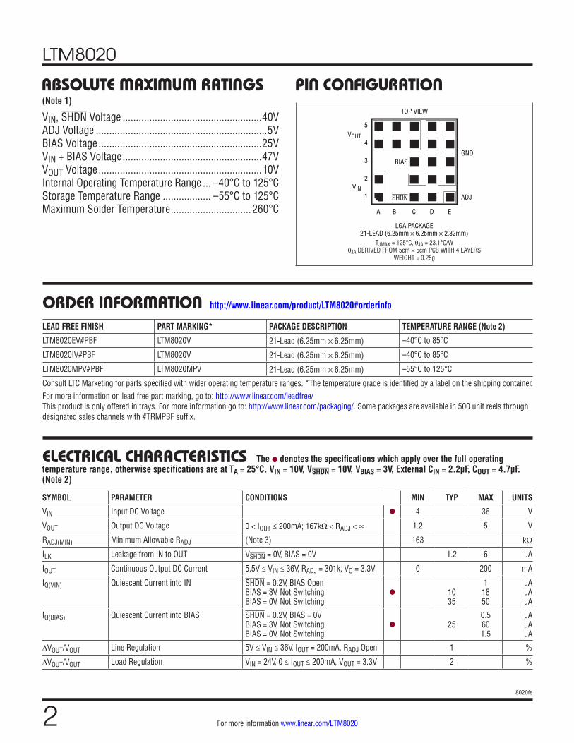
PIN CONFIGURATIONABSOLUTE MAXIMUM RATINGS
VIN, SHDN Voltage ....................................................40VADJ Voltage ................................................................5VBIAS Voltage .............................................................25VVIN + BIAS Voltage ....................................................47VVOUT Voltage .............................................................10VInternal Operating Temperature Range ... –40°C to 125°CStorage Temperature Range .................. –55°C to 125°CMaximum Solder Temperature .............................. 260°C
(Note 1)TOP VIEW
5
1
2
3
4
EA B C D
SHDN
GND
ADJ
VOUT
BIAS
VIN
LGA PACKAGE21-LEAD (6.25mm × 6.25mm × 2.32mm)
TJMAX = 125°C, θJA = 23.1°C/W θJA DERIVED FROM 5cm × 5cm PCB WITH 4 LAYERS
WEIGHT = 0.25g
LEAD FREE FINISH PART MARKING* PACKAGE DESCRIPTION TEMPERATURE RANGE (Note 2)
LTM8020EV#PBF LTM8020V 21-Lead (6.25mm × 6.25mm) –40°C to 85°C
LTM8020IV#PBF LTM8020V 21-Lead (6.25mm × 6.25mm) –40°C to 85°C
LTM8020MPV#PBF LTM8020MPV 21-Lead (6.25mm × 6.25mm) –55°C to 125°C
Consult LTC Marketing for parts specified with wider operating temperature ranges. *The temperature grade is identified by a label on the shipping container.For more information on lead free part marking, go to: http://www.linear.com/leadfree/ This product is only offered in trays. For more information go to: http://www.linear.com/packaging/. Some packages are available in 500 unit reels through designated sales channels with #TRMPBF suffix.
ORDER INFORMATION http://www.linear.com/product/LTM8020#orderinfo
ELECTRICAL CHARACTERISTICS
SYMBOL PARAMETER CONDITIONS MIN TYP MAX UNITS
VIN Input DC Voltage l 4 36 V
VOUT Output DC Voltage 0 < IOUT ≤ 200mA; 167kW < RADJ < ∞ 1.2 5 V
RADJ(MIN) Minimum Allowable RADJ (Note 3) 163 kW
ILK Leakage from IN to OUT VSHDN = 0V, BIAS = 0V 1.2 6 µA
IOUT Continuous Output DC Current 5.5V ≤ VIN ≤ 36V, RADJ = 301k, VO = 3.3V 0 200 mA
IQ(VIN) Quiescent Current into IN SHDN = 0.2V, BIAS Open BIAS = 3V, Not Switching BIAS = 0V, Not Switching
l
10 35
1 18 50
µA µA µA
IQ(BIAS) Quiescent Current into BIAS SHDN = 0.2V, BIAS = 0V BIAS = 3V, Not Switching BIAS = 0V, Not Switching
l
25
0.5 60 1.5
µA µA µA
DVOUT/VOUT Line Regulation 5V ≤ VIN ≤ 36V, IOUT = 200mA, RADJ Open 1 %
DVOUT/VOUT Load Regulation VIN = 24V, 0 ≤ IOUT ≤ 200mA, VOUT = 3.3V 2 %
The l denotes the specifications which apply over the full operating temperature range, otherwise specifications are at TA = 25°C. VIN = 10V, VSHDN = 10V, VBIAS = 3V, External CIN = 2.2µF, COUT = 4.7µF. (Note 2)
LTM8020
38020fe
For more information www.linear.com/LTM8020
ILOAD (mA)
EFFI
CIEN
CY (%
)
90
80
70
60
50
40
30
20
10
00.1 10 100 1000
8020 G03
1
12VIN24VIN36VIN
ILOAD (mA)
EFFI
CIEN
CY (%
)
90
80
70
60
50
40
30
20
10
00.1 10 100 1000
8020 G01
1
5VIN12VIN24VIN36VIN
ELECTRICAL CHARACTERISTICS
Note 1: Stresses beyond those listed under Absolute Maximum Ratings may cause permanent damage to the device. Exposure to any Absolute Maximum Rating condition for extended periods may affect device reliability and lifetime.Note 2: The LTM8020E is guaranteed to meet performance specifications from 0°C to 85°C ambient. Specifications over the full –40°C to 85°C ambient operating temperature range are assured by design, characterization and correlation with statistical process controls. The
The l denotes the specifications which apply over the full operating temperature range, otherwise specifications are at TA = 25°C. VIN = 10V, VSHDN = 10V, VBIAS = 3V, External CIN = 2.2µF, COUT = 4.7µF. (Note 2)
SYMBOL PARAMETER CONDITIONS MIN TYP MAX UNITS
VOUT(AC_RMS) Output Ripple (RMS) IOUT = 100mA, VOUT = 3.3V, VIN = 24V 7.5 mV
fSW Switching Frequency IOUT = 200mA 450 kHz
ISC Output Short-Circuit Current VIN = 36V, VOUT = 0V 350 mA
VADJ Voltage at ADJ Pin l 1.228 1.265 V
VBIAS(MIN) Minimum BIAS Voltage for Proper Operation
l 3 V
IADJ Current Out of ADJ Pin ADJ = 0V, VOUT = 5V, VSHDN = 0V l 9.65 10.35 µA
ISHDN SHDN Pin Current VSHDN = 2.5V 1 5 µA
VIH(SHDN) SHDN Input High Voltage 2.5 V
VIL(SHDN) SHDN Input Low Voltage 0.2 V
LTM8020I is guaranteed to meet specifications over the full –40°C to 85°C ambient operating temperature range. The LTM8020MP is guaranteed to meet specifications over the full –55°C to 125°C internal operating temperature range. Note that the maximum internal temperature is determined by specific operating conditions in conjunction with board layout, the rated package thermal resistance and other environmental factors.Note 3: Guaranteed by design.
TYPICAL PERFORMANCE CHARACTERISTICS
3.3VOUT Efficiency
3.3VOUT Power Loss
5VOUT Efficiency
IOUT (mA)
POW
ER L
OSS
(mW
)
1000
100
10
1
0.10.1 10 100 1000
8020 G02
1
5VIN12VIN24VIN36VIN
TA = 25°C unless otherwise noted.

LTM8020
48020fe
For more information www.linear.com/LTM8020
OUTPUT VOLTAGE (V)1
2
INPU
T VO
LTAG
E (V
)
3
4
5
6
2 3 4 5
4356 G12
7
8TO START
IOUT = 200mA
TO RUN
INPUT VOLTAGE (V)0
0
INPU
T CU
RREN
T (m
A)
20
40
60
80
10 20 30 40
4356 G10
100
0.18
0.16
0.14
0.12
0.10
0.08
0.06
0.04
0.02
0
OUTPUT CURRENT (A)0
INPU
T CU
RREN
T (A
)
0.05 0.10 0.15 0.20
4356 G05
1.8VOUT2.5VOUT3.3VOUT
OUTPUT CURRENT (A)0
0
INPU
T CU
RREN
T (A
)
0.010
0.020
0.030
0.040
0.05 0.10 0.15 0.20
4356 G07
0.050
0.0601.8VOUT2.5VOUT3.3VOUT5VOUT
IOUT (mA)
POW
ER L
OSS
(mW
)
1000
100
10
1
0.10.1 10 100 1000
8020 G04
1
12VIN24VIN36VIN
TYPICAL PERFORMANCE CHARACTERISTICS
Input Current vs Output Current (24VIN)
Input Quiescent Current vs Input Voltage
Input Current vs Input Voltage (Output Short)
Minimum Required Input Voltage vs Load (VOUT = 3.3V)
5VOUT Power Loss
Input Current vs Output Current (5VIN)
Input Current vs Output Current (12VIN)
OUTPUT CURRENT (A)0
0
INPU
T CU
RREN
T (A
)
0.020
0.040
0.060
0.080
0.05 0.10 0.15 0.20
4356 G06
0.100
0.1201.8VOUT2.5VOUT3.3VOUT5VOUT
OUTPUT CURRENT (A)0
0
INPU
T CU
RREN
T (A
)
0.010
0.020
0.005
0.015
0.025
0.030
0.040
0.05 0.10 0.15 0.20
4356 G08
0.035
0.0451.8VOUT2.5VOUT3.3VOUT5VOUT
Input Current vs Output Current (36VIN)
INPUT VOLTAGE (V)0
0
QUIE
SCEN
T CU
RREN
T (µ
A)
1
2
3
4
10 20 30 40
4356 G09
5
Minimum Required Input Voltage vs Output Voltage
LOAD CURRENT (mA)0
3.0
INPU
T VO
LTAG
E (V
)
3.5
4.0
4.5
5.0
50 100 150 200
4356 G11
5.5
6.0
SHDN CONTROL
TO START
TO RUN
TA = 25°C unless otherwise noted.

LTM8020
58020fe
For more information www.linear.com/LTM8020
PIN FUNCTIONSVIN (Pins A1, A2): The VIN pins supply current to the LTM8020’s internal regulator and to the internal power switch. These pins must be locally bypassed with an external, low ESR capacitor of at least 1µF.
VOUT (Pins A4, A5, B4, B5, C4, C5): Power Output Pins. An external capacitor is connected from VOUT to GND in most applications. Apply output load between these pins and GND.
BIAS (Pin C3): The BIAS pin connects to the internal boost Schottky diode and to the internal regulator. Tie to VOUT when VOUT > 3V or to another DC voltage greater than 3V otherwise. When BIAS > 3V the internal circuitry will be powered from this pin to improve efficiency. Main regulator power will still come from VIN.
SHDN (Pin C1): The SHDN pin is used to put the LTM8020 in shutdown mode. Tie to ground to shut down the LTM8020. Apply 2V or more for normal operation. If the shutdown feature is not used, tie this pin to VIN.
GND (Pins C2, D1, D2, D3, D4, D5, E2, E3, E4, E5): The GND connections serve as the main signal return and the primary heat sink for the LTM8020. Tie the GND pins to a local ground plane below the LTM8020 and the circuit components. Return the feedback divider to this signal.
ADJ (Pin E1): The LTM8020 regulates its ADJ pin to 1.25V. Connect the adjust resistor from this pin to GND. The value of this adjust resistor is determined by the equation RADJ = 623.75/(VOUT – 1.25), where RADJ is in kW. Note that the ADJ pin is open circuit if VOUT = 1.25V.
TYPICAL PERFORMANCE CHARACTERISTICS TA = 25°C unless otherwise noted.
INPUT VOLTAGE (V)0
0
TEM
PERA
TURE
RIS
E (°
C)
5
10
15
20
10 20 30 5040
8020 G13
25
3.3VOUT
5VOUT
Temperature Rise vs Input Voltage (Full Load, TA = 25°C)
Turn-On Behavior (6VIN, 3.3VOUT, No Load)
VOUT2V/DIV
SHDN5V/DIV
INPUT CURRENT100mA/DIV
50µs/DIV 8020 G14
FREQUENCY (MHz)0
EMIS
SION
S LE
VEL
(dBµ
V/m
)
50
70
90
800
8020 G15
30
10
40
60
80
20
0
–10200 400 600 1000
36VIN5VOUTFULL LOAD
EN55022CLASS B LIMIT
Radiated Emissions

LTM8020
68020fe
For more information www.linear.com/LTM8020
CURRENTMODE
CONTROLLER
8020 BD
22µH
0.1µF 10µF15pF 499k
BIAS
ADJGND
SHDN
VIN VOUT
BLOCK DIAGRAM

LTM8020
78020fe
For more information www.linear.com/LTM8020
OPERATIONThe LTM8020 is a standalone nonisolated step-down switching DC/DC power supply. It can deliver up to 200mA of DC output current with only bulk external input and output capacitors. This module provides a precisely regulated output voltage programmable via one external resistor from 1.25VDC to 5VDC. The input voltage range is 4V to 36V. Given that the LTM8020 is a step-down con-verter, make sure that the input voltage is high enough to support the desired output voltage and load current. See Block Diagram.
The LTM8020 contains a current mode controller, power switching element, power inductor, power Schottky diode and a modest amount of input and output capacitance. For some applications, as shown in Table 1, no output capacitor is necessary.
With its high performance current mode controller and internal feedback loop compensation, the LTM8020 module has sufficient stability margin and good transient perfor-mance under a wide range of operating conditions with a wide range of output capacitors, even all ceramic ones (X5R or X7R). Current mode control provides cycle-by-cycle fast current limit, and automatic current limiting protects the module in the event of a short circuit or overload fault.
The LTM8020 is built upon a variable frequency control-ler. The on time, off time and switching frequency are dependent upon the input voltage, output voltage and load current.
The drive circuit for the internal power switching element is powered through the BIAS pin. Power this pin with at least 3V.
The LTM8020 is equipped with two operating modes, dependant upon the load current. When the load current is sufficiently high, the LTM8020 will switch continuously (see Figure 1a). If the load is very light, or if the input voltage is high relative to the output voltage, the part will operate in Burst Mode® operation, alternating between its micropower and switching states to keep the output in regulation and hold the power dissipation to a minimum (See Figure 1b).
If the SHDN pin is grounded, all internal circuits are turned off and VIN current reduces to the device leakage current, typically a few nanoamps.
Figure 1. Output Voltage and Internal Inductor Current
VOUT20mV/DIV
IL100mA/DIV
1ms/DIV
VOUT20mV/DIV
IL100mA/DIV
5µs/DIV 8020 F01b
NO LOAD
10mA LOAD
(1b) Burst Mode Operation
VOUT20mV/DIV
IL100mA/DIV
1µs/DIV
VOUT20mV/DIV
IL100mA/DIV
1µs/DIV
(1a) Continuous Operation
8020 F1a
200mA LOAD
150mA LOAD
LTM8020
88020fe
For more information www.linear.com/LTM8020
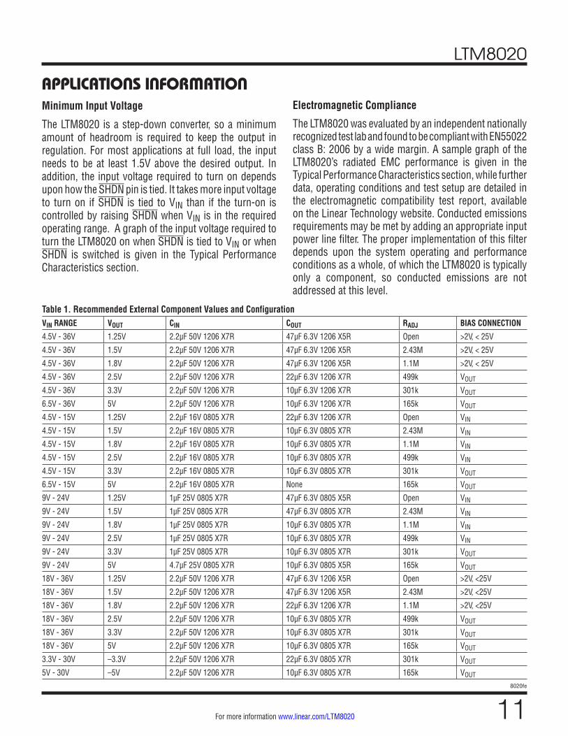
For most applications, the design process is straight forward, summarized as follows:
1. Look at Table 1 and find the row that has the desired input range and output voltage.
2. Apply the CIN, COUT, RADJ and BIAS connection indicated on that row.
While these component combinations have been tested for proper operation, it is incumbent upon the user to verify proper operation over the intended system’s line, load and environmental conditions.
If an output voltage other than those listed in Table 1 is desired, use the equation RADJ = 623.75/(VOUT – 1.25), where RADJ is in kW. As a starting point, use values for CIN and COUT that correspond to the input voltage and output voltage that most closely matches the intended application, and verify proper operation over the system’s line, load and environmental conditions.
Capacitor Selection Considerations
The CIN and COUT capacitor values in Table 1 are the minimum recommended values for the associated oper-ating conditions. Applying capacitor values below those indicated in Table 1 is not recommended, and may result in undesirable operation. An input system bulk capacitor is assumed. Using larger values is generally acceptable, and can yield improved dynamic response, if it is neces-sary. Again, it is incumbent upon the user to verify proper operation over the intended system’s line, load and envi-ronmental conditions.
Ceramic capacitors are small, robust and have very low ESR. However, not all ceramic capacitors are suitable. X5R and X7R types are stable over temperature and ap-plied voltage and give dependable service. Other types, including Y5V and Z5U have very large temperature and voltage coefficients of capacitance. In an application cir-cuit they may have only a small fraction of their nominal capacitance resulting in much higher output voltage ripple than expected.
Ceramic capacitors are also piezoelectric. The LTM8020’s switching frequency depends on the load current, and at light loads it can excite a ceramic capacitor at audio
APPLICATIONS INFORMATIONfrequencies, generating audible noise. Since the LTM8020 operates at a lower current limit during Burst Mode opera-tion, the noise is typically very quiet to a casual ear.
If this audible noise is unacceptable, use a high performance electrolytic capacitor at the output. The input capacitor can be a parallel combination of a 2.2µF ceramic capacitor and a low cost electrolytic capacitor.
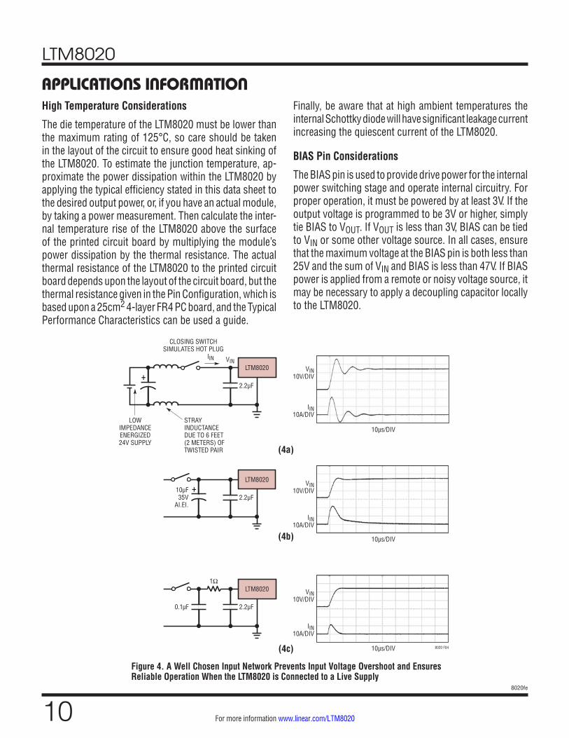
A final precaution regarding ceramic capacitors concerns the maximum input voltage rating of the LTM8020. A ceramic input capacitor combined with trace or cable inductance forms a high Q (under damped) tank circuit. If the LTM8020 circuit is plugged into a live supply, the input voltage can ring to twice its nominal value, possi-bly exceeding the device’s rating. This situation is easily avoided; see the Hot-Plugging Safely section.
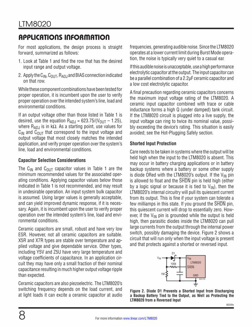
Shorted Input Protection
Care needs to be taken in systems where the output will be held high when the input to the LTM8020 is absent. This may occur in battery charging applications or in battery backup systems where a battery or some other supply is diode ORed with the LTM8020’s output. If the VIN pin is allowed to float and the SHDN pin is held high (either by a logic signal or because it is tied to VIN), then the LTM8020’s internal circuitry will pull its quiescent current from its output. This is fine if your system can tolerate a few milliamps in this state. If you ground the SHDN pin, this quiescent current will drop to essentially zero. How-ever, if the VIN pin is grounded while the output is held high, then parasitic diodes inside the LTM8020 can pull large currents from the output through the internal power switch, possibly damaging the device. Figure 2 shows a circuit that will run only when the input voltage is present and that protects against a shorted or reversed input.
Figure 2. Diode D1 Prevents a Shorted Input from Discharging a Backup Battery Tied to the Output, as Well as Protecting the LTM8020 from a Reversed Input
VINLTM8020
SHDN
VIN
8020 F02
GND
D1
100k
1M

LTM8020
98020fe
For more information www.linear.com/LTM8020
APPLICATIONS INFORMATIONPCB Layout
Most of the headaches associated with PCB layout have been alleviated or even eliminated by the high level of integration of the LTM8020. The LTM8020 is never-the-less a switching power supply, and care must be taken to minimize EMI and ensure proper operation. Even with the high level of integration, you may fail to achieve specified operation with a haphazard or poor layout. See Figure 3 for a suggested layout.
Ensure that the grounding and heat sinking are acceptable. A few rules to keep in mind are:
1. Place the CIN capacitor as close as possible to the VIN and GND connection of the LTM8020.
2. Place the COUT capacitor as close as possible to the VOUT and GND connection of the LTM8020.
3. Place the CIN and COUT capacitors such that their ground current flows directly adjacent or underneath the LTM8020.
4. Connect all of the GND connections to as large a copper pour or plane area as possible on the top layer. Avoid breaking the ground connection between the external components and the LTM8020.
5. The copper pours also serve as the heat sink for the LTM8020. Place several vias in the GND plane to act as heat pipes to other layers of the printed circuit board.
Positive-to-Negative Voltage Regulation
The LTM8020 can generate a negative output by tying the VOUT pads to system ground and connecting GND as shown in the Typical Applications section. In this configuration, SHDN must be level shifted or referenced to GND, and the available output current may be reduced.
Hot-Plugging Safely
The small size, robustness and low impedance of ceramic capacitors make them an attractive option for the input bypass capacitor of LTM8020. However, these capacitors can cause problems if the LTM8020 is plugged into a live supply (see Linear Technology Application Note 88 for a complete discussion). The low loss ceramic capacitor combined with stray inductance in series with the power source forms an under damped tank circuit, and the volt-age at the VIN pin of the LTM8020 can ring to twice the nominal input voltage, possibly exceeding the LTM8020’s rating and damaging the part. If the input supply is poorly controlled or the user will be plugging the LTM8020 into an energized supply, the input network should be designed to prevent this overshoot. Figure 4 shows the waveforms that result when an LTM8020 circuit is connected to a 24V supply through six feet of 24-gauge twisted pair. The first plot is the response with a 2.2µF ceramic capacitor at the input. The input voltage rings as high as 35V and the input current peaks at 20A. One method of damping the tank circuit is to add another capacitor with a series resistor to the circuit. In Figure 4b an aluminum electrolytic capacitor has been added. This capacitor’s high equivalent series resistance damps the circuit and eliminates the voltage overshoot. The extra capacitor improves low frequency ripple filtering and can slightly improve the efficiency of the circuit, though it is likely to be the largest component in the circuit. An alternative solution is shown in Figure 4c. A 1W resistor is added in series with the input to eliminate the voltage overshoot (it also reduces the peak input current). A 0.1µF capacitor improves high frequency filtering. This solution is smaller and less expensive than the electrolytic capacitor. For high input voltages its impact on efficiency is minor, reducing efficiency less than one-half percent for a 5V output at full load operating from 24V.
Figure 3. Layout Showing Suggested External Components, GND Plane and Thermal Vias
GND
VIAs TO GND PLANE
VOUT
ADJ
COPPER
BIASSHDN
VIN
COUT
RADJ
CIN
8020 F03
LTM8020
108020fe
For more information www.linear.com/LTM8020
High Temperature Considerations
The die temperature of the LTM8020 must be lower than the maximum rating of 125°C, so care should be taken in the layout of the circuit to ensure good heat sinking of the LTM8020. To estimate the junction temperature, ap-proximate the power dissipation within the LTM8020 by applying the typical efficiency stated in this data sheet to the desired output power, or, if you have an actual module, by taking a power measurement. Then calculate the inter-nal temperature rise of the LTM8020 above the surface of the printed circuit board by multiplying the module’s power dissipation by the thermal resistance. The actual thermal resistance of the LTM8020 to the printed circuit board depends upon the layout of the circuit board, but the thermal resistance given in the Pin Configuration, which is based upon a 25cm2 4-layer FR4 PC board, and the Typical Performance Characteristics can be used a guide.
Finally, be aware that at high ambient temperatures the internal Schottky diode will have significant leakage current increasing the quiescent current of the LTM8020.
BIAS Pin Considerations
The BIAS pin is used to provide drive power for the internal power switching stage and operate internal circuitry. For proper operation, it must be powered by at least 3V. If the output voltage is programmed to be 3V or higher, simply tie BIAS to VOUT. If VOUT is less than 3V, BIAS can be tied to VIN or some other voltage source. In all cases, ensure that the maximum voltage at the BIAS pin is both less than 25V and the sum of VIN and BIAS is less than 47V. If BIAS power is applied from a remote or noisy voltage source, it may be necessary to apply a decoupling capacitor locally to the LTM8020.
APPLICATIONS INFORMATION
Figure 4. A Well Chosen Input Network Prevents Input Voltage Overshoot and Ensures Reliable Operation When the LTM8020 is Connected to a Live Supply
+LTM8020
2.2µF
VIN10V/DIV
IIN10A/DIV
VIN10V/DIV
IIN10A/DIV
VIN10V/DIV
IIN10A/DIV
10µs/DIV
10µs/DIV
10µs/DIV
VIN
CLOSING SWITCHSIMULATES HOT PLUG
IIN
(4a)
(4b)
(4c)
LOWIMPEDANCEENERGIZED24V SUPPLY
STRAYINDUCTANCEDUE TO 6 FEET(2 METERS) OFTWISTED PAIR
+LTM8020
2.2µF10µF35V
AI.EI.
LTM8020
2.2µF0.1µF
1Ω
8020 F04
LTM8020
118020fe
For more information www.linear.com/LTM8020
APPLICATIONS INFORMATION
Table 1. Recommended External Component Values and ConfigurationVIN RANGE VOUT CIN COUT RADJ BIAS CONNECTION
4.5V - 36V 1.25V 2.2µF 50V 1206 X7R 47µF 6.3V 1206 X5R Open >2V, < 25V
4.5V - 36V 1.5V 2.2µF 50V 1206 X7R 47µF 6.3V 1206 X5R 2.43M >2V, < 25V
4.5V - 36V 1.8V 2.2µF 50V 1206 X7R 47µF 6.3V 1206 X5R 1.1M >2V, < 25V
4.5V - 36V 2.5V 2.2µF 50V 1206 X7R 22µF 6.3V 1206 X7R 499k VOUT
4.5V - 36V 3.3V 2.2µF 50V 1206 X7R 10µF 6.3V 1206 X7R 301k VOUT
6.5V - 36V 5V 2.2µF 50V 1206 X7R 10µF 6.3V 1206 X7R 165k VOUT
4.5V - 15V 1.25V 2.2µF 16V 0805 X7R 22µF 6.3V 1206 X7R Open VIN
4.5V - 15V 1.5V 2.2µF 16V 0805 X7R 10µF 6.3V 0805 X7R 2.43M VIN
4.5V - 15V 1.8V 2.2µF 16V 0805 X7R 10µF 6.3V 0805 X7R 1.1M VIN
4.5V - 15V 2.5V 2.2µF 16V 0805 X7R 10µF 6.3V 0805 X7R 499k VIN
4.5V - 15V 3.3V 2.2µF 16V 0805 X7R 10µF 6.3V 0805 X7R 301k VOUT
6.5V - 15V 5V 2.2µF 16V 0805 X7R None 165k VOUT
9V - 24V 1.25V 1µF 25V 0805 X7R 47µF 6.3V 0805 X5R Open VIN
9V - 24V 1.5V 1µF 25V 0805 X7R 47µF 6.3V 0805 X7R 2.43M VIN
9V - 24V 1.8V 1µF 25V 0805 X7R 10µF 6.3V 0805 X7R 1.1M VIN
9V - 24V 2.5V 1µF 25V 0805 X7R 10µF 6.3V 0805 X7R 499k VIN
9V - 24V 3.3V 1µF 25V 0805 X7R 10µF 6.3V 0805 X7R 301k VOUT
9V - 24V 5V 4.7µF 25V 0805 X7R 10µF 6.3V 0805 X5R 165k VOUT
18V - 36V 1.25V 2.2µF 50V 1206 X7R 47µF 6.3V 1206 X5R Open >2V, <25V
18V - 36V 1.5V 2.2µF 50V 1206 X7R 47µF 6.3V 1206 X5R 2.43M >2V, <25V
18V - 36V 1.8V 2.2µF 50V 1206 X7R 22µF 6.3V 1206 X7R 1.1M >2V, <25V
18V - 36V 2.5V 2.2µF 50V 1206 X7R 10µF 6.3V 0805 X7R 499k VOUT
18V - 36V 3.3V 2.2µF 50V 1206 X7R 10µF 6.3V 0805 X7R 301k VOUT
18V - 36V 5V 2.2µF 50V 1206 X7R 10µF 6.3V 0805 X7R 165k VOUT
3.3V - 30V –3.3V 2.2µF 50V 1206 X7R 22µF 6.3V 0805 X7R 301k VOUT
5V - 30V –5V 2.2µF 50V 1206 X7R 10µF 6.3V 0805 X7R 165k VOUT
Minimum Input Voltage
The LTM8020 is a step-down converter, so a minimum amount of headroom is required to keep the output in regulation. For most applications at full load, the input needs to be at least 1.5V above the desired output. In addition, the input voltage required to turn on depends upon how the SHDN pin is tied. It takes more input voltage to turn on if SHDN is tied to VIN than if the turn-on is controlled by raising SHDN when VIN is in the required operating range. A graph of the input voltage required to turn the LTM8020 on when SHDN is tied to VIN or when SHDN is switched is given in the Typical Performance Characteristics section.
Electromagnetic Compliance
The LTM8020 was evaluated by an independent nationally recognized test lab and found to be compliant with EN55022 class B: 2006 by a wide margin. A sample graph of the LTM8020’s radiated EMC performance is given in the Typical Performance Characteristics section, while further data, operating conditions and test setup are detailed in the electromagnetic compatibility test report, available on the Linear Technology website. Conducted emissions requirements may be met by adding an appropriate input power line filter. The proper implementation of this filter depends upon the system operating and performance conditions as a whole, of which the LTM8020 is typically only a component, so conducted emissions are not addressed at this level.

LTM8020
128020fe
For more information www.linear.com/LTM8020
VIN (V)0
0
I LOA
D (m
A)
50
100
150
200
10 155 20 3025
8020 TA08
250VIN VOUT
LTM8020
BIASSHDN
10µFX5R
165k1%
2.2µF
–5V
VIN*5V TO 30V
8020 TA06
ADJ GND –5V85mA
OPTIONALSCHOTTKYCLAMP
–5V Positive-to-Negative Converter
VIN VOUTLTM8020
BIASSHDN
165k1%
2.2µF
VIN*6.5V TO 15V
8020 TA05
GND ADJ
VOUT5V200mA
5V Step-Down Converter (No Output Capacitor Required)
TYPICAL APPLICATIONS
VIN VOUTLTM8020
SHDN
47µFX5R
1µF
VIN*4.5V TO 24V
8020 TA02
GND ADJ
VOUT1.25V200mA
BIAS
VIN VOUTLTM8020
BIASSHDN
10µFX5R
301k1%
1µF
VIN*4.5V TO 36V
8020 TA04
GND ADJ
VOUT3.3V200mA
1.25V Step-Down Converter 3.3V Step-Down Converter
VIN VOUTLTM8020
SHDNBIAS 22µF
X7R
1.1M1%
2.2µF
VIN*4.5V TO 15V
8020 TA03
GND ADJ
VOUT1.8V200mA
1.8V Step-Down Converter
–5V Positive-to-Negative Converter Output vs Input Voltage
*
* RUNNING VOLTAGE RANGE. PLEASE REFER TO APPLICATIONS INFORMATION FOR START-UP DETAILS

LTM8020
138020fe
For more information www.linear.com/LTM8020
PACKAGE DESCRIPTION
NOTE
S:1.
DIM
ENSI
ONIN
G AN
D TO
LERA
NCIN
G PE
R AS
ME
Y14.
5M-1
994
2. A
LL D
IMEN
SION
S AR
E IN
MIL
LIM
ETER
S
LAN
D DE
SIGN
ATIO
N PE
R JE
SD M
O-22
2, S
PP-0
10 A
ND S
PP-0
20
5. P
RIM
ARY
DATU
M -Z
- IS
SEAT
ING
PLAN
E
6. T
HE T
OTAL
NUM
BER
OF P
ADS:
21
43
DETA
ILS
OF P
AD #
1 ID
ENTI
FIER
ARE
OPT
IONA
L,BU
T M
UST
BE L
OCAT
ED W
ITHI
N TH
E ZO
NE IN
DICA
TED.
THE
PAD
#1 ID
ENTI
FIER
MAY
BE
EITH
ER A
MOL
D OR
A
MAR
KED
FEAT
URE
SYM
BOL
aaa
bbb
TOLE
RANC
E0.
150.
102.22
– 2
.42
DETA
IL A
PACK
AGE
SIDE
VIE
W
DETA
IL A
SUBS
TRAT
EM
OLD
CAP
0.27
– 0
.37
2.5400
2.5400
1.2700
1.2700
0.0000
1.95
– 2
.05
bbb Z
Z
6.25
0BS
C
PACK
AGE
TOP
VIEW
LGA
21 0
113
REV
B
6.25
0BS
C
4
PAD
1CO
RNER
3PADS
SEE
NOTE
S
XY
aaa
Z
aaa
Z
2.54
00
1.58
75
0.95
251.
2700
0.3175
0.31750.0000
2.54
00
SUGG
ESTE
D PC
B LA
YOUT
TOP
VIEW
1.27
00
0.00
00
1.27
OBS
C
0.60
5 –
0.66
5
0.60
5 –
0.66
5
5.08
0
5.08
0BS
C
C(0.
30)
PAD
1
EA
5 1234
BC
BOTT
OM V
IEW
D
LTM
XXXX
XXµM
odul
e
TRAY
PIN
1BE
VEL
PACK
AGE
IN T
RAY
LOAD
ING
ORIE
NTAT
ION
COM
PONE
NTPI
N “A
1”
LGA
Pack
age
21-L
ead
(6.2
5mm
× 6
.25m
m ×
2.3
2mm
)(R
efer
ence
LTC
DW
G #
05-0
8-18
03 R
ev B
)
7PA
CKAG
E RO
W A
ND C
OLUM
N LA
BELI
NG M
AY V
ARY
AMON
G µM
odul
e PR
ODUC
TS. R
EVIE
W E
ACH
PACK
AGE
LAYO
UT C
AREF
ULLY
!
7
SEE
NOTE
S
Please refer to http://www.linear.com/product/LTM8020#packaging for the most recent package drawings.

LTM8020
148020fe
For more information www.linear.com/LTM8020
PACKAGE DESCRIPTION
LTM8020 Pinout (Sorted by Pin Number)PIN SIGNAL DESCRIPTION
A1 VIN
A2 VIN
A4 VOUT
A5 VOUT
B4 VOUT
B5 VOUT
C1 SHDN
C2 GND
C3 BIAS
C4 VOUT
C5 VOUT
D1 GND
D2 GND
D3 GND
D4 GND
D5 GND
E1 ADJ
E2 GND
E3 GND
E4 GND
E5 GND
LTM8020
158020fe
For more information www.linear.com/LTM8020
Information furnished by Linear Technology Corporation is believed to be accurate and reliable. However, no responsibility is assumed for its use. Linear Technology Corporation makes no representa-tion that the interconnection of its circuits as described herein will not infringe on existing patent rights.
REVISION HISTORYREV DATE DESCRIPTION PAGE NUMBER
D 3/10 Changes to Description and Features.Changes to Applications Information.“Electromagnetic Compliance” Paragraph Added to Applications Information.Changes to Typical Application.
18
1113
E 8/17 Corrected –5V circuit from IOUT of 85µA to 85mA. 12
(Revision history begins at Rev D)

LTM8020
168020fe
For more information www.linear.com/LTM8020 LINEAR TECHNOLOGY CORPORATION 2007
LT 0817 • PRINTED IN USAwww.linear.com/LTM8020
PART NUMBER DESCRIPTION COMMENTS
LTM4600 10A DC/DC µModule Basic 10A DC/DC µModule, 15mm × 15mm × 2.8mm LGA
LTM4600HVMPV Military Plastic 10A DC/DC µModule –55°C to 125°C Operation, 15mm × 15mm × 2.8mm LGA
LTM4601/LTM4601A
12A DC/DC µModule with PLL, Output Tracking/Margining and Remote Sensing
Synchronizable, PolyPhase Operation, LTM4601-1 Version has no Remote Sensing
LTM4602 6A DC/DC µModule Pin Compatible with the LTM4600
LTM4603 6A DC/DC µModule with PLL and Output Tracking/Margining and Remote Sensing
Synchronizable, PolyPhase Operation, LTM4603-1 Version has no Remote Sensing, Pin Compatible with the LTM4601
LTM4604 4A Low VIN DC/DC µModule 2.375V ≤ VIN ≤ 5V, 0.8V ≤ VOUT ≤ 5V, 9mm × 15mm × 2.3mm LGA
LTM4608 8A Low VIN DC/DC µModule 2.375V ≤ VIN ≤ 5V, 0.8V ≤ VOUT ≤ 5V, 9mm × 15mm × 2.8mm LGA
LTM8022 1A, 36V DC/DC µModule Adjustable Frequency, 0.8V ≤ VOUT ≤ 5V, 11.25mm × 9mm × 2.82mm, Pin Compatible to the LTM8023
LTM8023 2A, 36V DC/DC µModule Adjustable Frequency, 0.8V ≤ VOUT ≤ 5V, 11.25mm × 9mm × 2.82mm, Pin Compatible to the LTM8022
RELATED PARTS
TYPICAL APPLICATION
VIN VOUTLTM8020
BIASSHDN
10µFX5R
301k1%
1µF
VIN5V TO 36V
8020 TA07
GND ADJ
VOUT3.3V200mA
3.3V Step-Down Converter
*
*RUNNING VOLTAGE RANGE. PLEASE REFER TO APPLICATIONS INFORMATION FOR START-UP DETAILS
Related Documents


