LT8609S 1 Rev. D For more information www.analog.com Document Feedback TYPICAL APPLICATION FEATURES DESCRIPTION 42V, 2A/3A Peak Synchronous Step-Down Regulator with 2.5µA Quiescent Current The LT ® 8609S is a compact, high efficiency, high speed synchronous monolithic step-down switching regulator that consumes only 1.7µA of non-switching quiescent current. The LT8609S can deliver 2A of continuous cur- rent with peak loads of 3A (<1sec) to support applications such as GSM transceivers which require high transient loads. Top and bottom power switches are included with all necessary circuitry to minimize the need for external components. Low ripple Burst Mode operation enables high efficiency down to very low output currents while keeping the output ripple below 10mV P-P . A SYNC pin allows synchronization to an external clock, or spread spectrum modulation of switching frequencies for low EMI operation. Internal compensation with peak current mode topology allows the use of small inductors and results in fast transient response and good loop stability. The EN/UV pin has an accurate 1V threshold and can be used to program V IN undervoltage lockout or to shut down the LT8609S reducing the input supply current to 1µA. A capacitor on the TR/SS pin programs the output voltage ramp rate during start-up while the PG flag signals when V OUT is within ±8.5% of the programmed output voltage as well as fault conditions. The LT8609S is available in a small 16-lead 3mm × 3mm LQFN package. APPLICATIONS n Silent Switcher ® 2 Architecture n Ultralow EMI Emissions on Any PCB n Eliminates PCB Layout Sensitivity n Internal Bypass Capacitors Reduce Radiated EMI n Optional Spread Spectrum Modulation n Wide Input Voltage Range: 3.0V to 42V n Ultralow Quiescent Current Burst Mode ® Operation: n <2.5µA I Q Regulating 12V IN to 3.3V OUT n Output Ripple <10mV P-P n High Efficiency 2MHz Synchronous Operation: n >93% Efficiency at 1A, 12V IN to 5V OUT n 2A Maximum Continuous Output, 3A Peak Transient Output n Fast Minimum Switch-On Time: 45ns n Adjustable and Synchronizable: 200kHz to 2.2MHz n Allows Use of Small Inductors n Low Dropout n Peak Current Mode Operation n Internal Compensation n Output Soft-Start and Tracking n Small 16-Lead 3mm × 3mm LQFN Package n AEC-Q100 Qualified for Automotive Applications n General Purpose Step Down n Low EMI Step Down All registered trademarks and trademarks are the property of their respective owners. V IN EN/UV ON OFF 22μF 10pF 4.7μF V IN 5.5V TO 40V 1μF V OUT 5V 2A 182k 8609S TA01a 2.2μH 1M SYNC INTV CC TR/SS RT LT8609S GND SW PG FB 18.2k 5V, 2MHz Step Down 12V IN to 5V OUT Efficiency I OUT (A) 0 EFFICIENCY (%) 100 65 90 70 55 85 80 60 95 75 50 1.50 8609S TA01b 2.50 2.00 1.00 0.50 f SW = 2MHz

Welcome message from author
This document is posted to help you gain knowledge. Please leave a comment to let me know what you think about it! Share it to your friends and learn new things together.
Transcript

LT8609S
1Rev. D
For more information www.analog.comDocument Feedback
TYPICAL APPLICATION
FEATURES DESCRIPTION
42V, 2A/3A Peak Synchronous Step-Down Regulator
with 2.5µA Quiescent Current
The LT®8609S is a compact, high efficiency, high speed synchronous monolithic step-down switching regulator that consumes only 1.7µA of non-switching quiescent current. The LT8609S can deliver 2A of continuous cur-rent with peak loads of 3A (<1sec) to support applications such as GSM transceivers which require high transient loads. Top and bottom power switches are included with all necessary circuitry to minimize the need for external components. Low ripple Burst Mode operation enables high efficiency down to very low output currents while keeping the output ripple below 10mVP-P. A SYNC pin allows synchronization to an external clock, or spread spectrum modulation of switching frequencies for low EMI operation. Internal compensation with peak current mode topology allows the use of small inductors and results in fast transient response and good loop stability. The EN/UV pin has an accurate 1V threshold and can be used to program VIN undervoltage lockout or to shut down the LT8609S reducing the input supply current to 1µA. A capacitor on the TR/SS pin programs the output voltage ramp rate during start-up while the PG flag signals when VOUT is within ±8.5% of the programmed output voltage as well as fault conditions. The LT8609S is available in a small 16-lead 3mm × 3mm LQFN package. APPLICATIONS
n Silent Switcher® 2 Architecture n Ultralow EMI Emissions on Any PCB n Eliminates PCB Layout Sensitivity n Internal Bypass Capacitors Reduce Radiated EMI n Optional Spread Spectrum Modulation
n Wide Input Voltage Range: 3.0V to 42V n Ultralow Quiescent Current Burst Mode® Operation:
n <2.5µA IQ Regulating 12VIN to 3.3VOUT n Output Ripple <10mVP-P
n High Efficiency 2MHz Synchronous Operation: n >93% Efficiency at 1A, 12VIN to 5VOUT
n 2A Maximum Continuous Output, 3A Peak Transient Output
n Fast Minimum Switch-On Time: 45ns n Adjustable and Synchronizable: 200kHz to 2.2MHz n Allows Use of Small Inductors n Low Dropout n Peak Current Mode Operation n Internal Compensation n Output Soft-Start and Tracking n Small 16-Lead 3mm × 3mm LQFN Package n AEC-Q100 Qualified for Automotive Applications
n General Purpose Step Down n Low EMI Step Down
All registered trademarks and trademarks are the property of their respective owners.
VINEN/UVON OFF
22µF
10pF
4.7µF
VIN5.5V TO 40V
1µF
VOUT5V2A
182k
8609S TA01a
2.2µH
1M
SYNC
INTVCCTR/SSRT
LT8609S
GND
SW
PGFB
18.2k
5V, 2MHz Step Down
12VIN to 5VOUT Efficiency
IOUT (A)0
EFFI
CIEN
CY (%
)
100
65
90
70
55
85
80
60
95
75
501.50
8609S TA01b
2.502.001.000.50
fSW = 2MHz

LT8609S
2Rev. D
For more information www.analog.com
PIN CONFIGURATIONABSOLUTE MAXIMUM RATINGS
VIN, EN/UV, PG ..........................................................42VFB, TR/SS . .................................................................4VSYNC Voltage . ............................................................6VOperating Junction Temperature Range (Note 2) LT8609SE .............................................. –40 to 125°C LT8609SI ............................................... –40 to 125°CStorage Temperature Range ......................–65 to 150°CMaximum Reflow (Package Body)
Temperature ...................................................... 260°C
(Note 1)
12
11
10
9
N/C
RT
VCC
GND
GND
N/C
N/C
PG
EN/UV
VIN
VIN
N/C
SW SW N/C
GND
SYNC
TR/S
S
GND
FB
1
2
3
4
16 15 14 13
5 6 7 8
TOP VIEW
LQFN PACKAGE16-LEAD (3mm × 3mm) LQFN
JEDEC BOARD: θJA = 50°C/W, θJC(PAD) = 14°C/W (NOTE 4)DEMOBOARD: θJA = 31°C/W
EXPOSED PAD (PIN 17) IS GND, MUST BE SOLDERED TO PCB
17GND
ORDER INFORMATION
PART NUMBER TAPE AND REELPART
MARKING*FINISH CODE
PAD FINISH
PACKAGE TYPE**
MSL RATING TEMPERATURE RANGE
LT8609SEV#PBF LT8609SEV#TRPBF LGYNe4 Au
(RoHS)LQFN (Laminate Package
with QFN Footprint 3–40°C to 125°C
LT8609SIV#PBF LT8609SIV#TRPBF LGYN –40°C to 125°C
AUTOMOTIVE PRODUCTS**
LT8609SEV#WPBF LT8609SEV#WTRPBF LGYNe4 Au
(RoHS)LQFN (Laminate Package
with QFN Footprint 3–40°C to 125°C
LT8609SIV#WPBF LT8609SIV#WTRPBF LGYN –40°C to 125°C
Contact the factory for parts specified with wider operating temperature ranges. *The temperature grade is identified by a label on the shipping container.• Pad or ball finish code is per IPC/JEDEC J-STD-609.• Recommended PCB Assembly and Manufacturing Procedures.• Package and Tray Drawings
• Parts ending with PBF are RoHS and WEEE compliant.** The LT8609S package has the same footprint as a standard 3mm × 3mm QFN Package.**Versions of this part are available with controlled manufacturing to support the quality and reliability requirements of automotive applications. These
models are designated with a #W suffix. Only the automotive grade products shown are available for use in automotive applications. Contact your local Analog Devices account representative for specific product ordering information and to obtain the specific Automotive Reliability reports for these models.
LT8609S
3Rev. D
For more information www.analog.com
ELECTRICAL CHARACTERISTICS The l denotes the specifications which apply over the full operating temperature range, otherwise specifications are at TA = 25°C.
Note 1: Stresses beyond those listed under Absolute Maximum Ratings may cause permanent damage to the device. Exposure to any Absolute Maximum Rating condition for extended periods may affect device reliability and lifetime. Absolute Maximum Ratings are those values beyond which the life of a device may be impaired.Note 2: The LT8609SE is guaranteed to meet performance specifications from 0°C to 125°C junction temperature. Specifications over the –40°C to 125°C operating junction temperature range are assured by design, characterization, and correlation with statistical process controls. The LT8609SI is guaranteed over the full –40°C to 125°C operating junction temperature range.
Note 3: This IC includes overtemperature protection that is intended to protect the device during overload conditions. Junction temperature will exceed 150°C when overtemperature protection is active. Continuous operation above the specified maximum operating junction temperature will reduce lifetime.Note 4: θ values determined per JEDEC 51-7, 51-12. See the Applications Information Section for information on improving the thermal resistance and for actual temperature measurements of a demo board in typical operating conditions.
PARAMETER CONDITIONS MIN TYP MAX UNITS
Minimum Input Voltage
l
2.7
3.0 3.2
V
VIN Quiescent Current VEN/UV = 0V, VSYNC = 0V VEN/UV = 2V, Not Switching, VSYNC = 0V, VIN ≤ 36V
l
1 1.7
5 12
µA µA
VIN Current in Regulation VIN = 6V, VOUT = 2.7V, Output Load = 100µA VIN = 6V, VOUT = 2.7V, Output Load = 1mA
l
l
46 480
90 700
µA µA
Feedback Reference Voltage VIN = 6V, ILOAD = 100mA VIN = 6V, ILOAD = 100mA
l
0.770 0.758
0.774 0.774
0.778 0.794
V V
Feedback Voltage Line Regulation VIN = 4.0V to 40V l 0.02 0.06 %/V
Feedback Pin Input Current VFB = 1V l ±20 nA
Minimum On-Time ILOAD = 1.75A, SYNC = 0V ILOAD = 1.75A, SYNC = 1.9V
l
l
45 45
75 60
ns ns
Minimum Off Time 90 130 ns
Oscillator Frequency RT = 221k, ILOAD = 0.5A RT = 60.4k, ILOAD = 0.5A RT = 18.2k, ILOAD = 0.5A
l
l
l
155 640
1.925
200 700 2.00
245 760
2.075
kHz kHz
MHz
Top Power NMOS On-Resistance ILOAD = 1A 185 mΩ
Top Power NMOS Current Limit l 3.4 4.75 5.7 A
Bottom Power NMOS On-Resistance 115 mΩ
SW Leakage Current VIN = 42V, VSW = 40V 5 µA
EN/UV Pin Threshold EN/UV Rising l 0.99 1.05 1.11 V
EN/UV Pin Hysteresis 50 mV
EN/UV Pin Current VEN/UV = 2V l ±20 nA
PG Upper Threshold Offset from VFB VFB Rising l 5.0 8.5 13.0 %
PG Lower Threshold Offset from VFB VFB Falling l 5.0 8.5 13.0 %
PG Hysteresis 0.5 %
PG Leakage VPG = 42V l ±200 nA
PG Pull-Down Resistance VPG = 0.1V 550 1200 Ω
Sync Low Input Voltage l 0.4 0.9 V
Sync High Input Voltage INTVCC = 3.5V l 2.7 3.2 V
TR/SS Source Current l 1 2 3 µA
TR/SS Pull-Down Resistance Fault Condition, TR/SS = 0.1V 300 900 Ω
Spread Spectrum Modulation Frequency VSYNC = 3.3V 0.5 3 6 kHz
LT8609S
4Rev. D
For more information www.analog.com
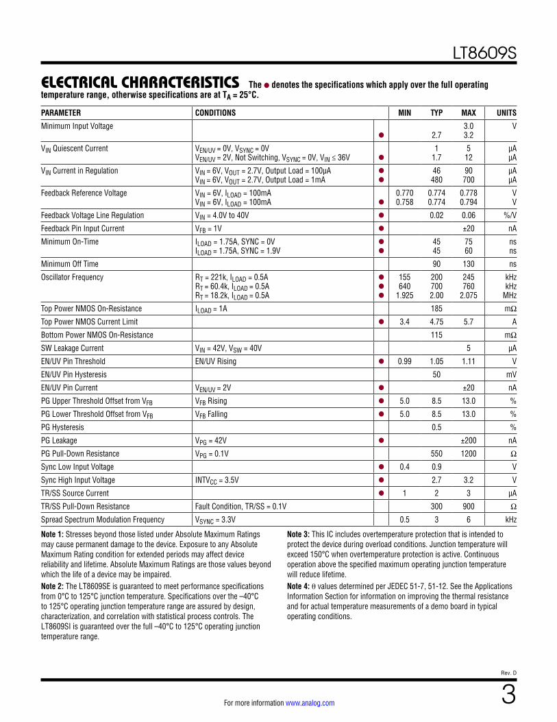
Efficiency (3.3V Output, 2MHz, Burst Mode Operation)
Efficiency (3.3V Output, 2MHz, Burst Mode Operation)
Efficiency (5V Output, 2MHz, Burst Mode Operation)
Efficiency (5V Output, 2MHz, Burst Mode Operation) FB Voltage Load Regulation
Line RegulationNo-Load Supply Current (3.3V Output)
fSW = 2MHz
VIN = 12V
VIN = 24V
L = 2.2µH
IOUT (mA)0.001 0.01 0.1 1 10 100 1k 10k0
10
20
30
40
50
60
70
80
90
100
EFFI
CIEN
CY (%
)
8609S G04TEMPERATURE (°C)
–50 –10 30 70 110 150768.0
769.0
770.0
771.0
772.0
773.0
774.0
775.0
776.0
777.0
778.0
FB R
EGUL
ATIO
N VO
LTAG
E (m
V)
8609S G05OUTPUT CURRENT (A)
0.0 0.25 0.5 0.75 1.0 1.25 1.5 1.75 2.0 2.25 2.5–0.50
–0.40
–0.30
–0.20
–0.10
0.00
0.10
0.20
0.30
0.40
0.50
CHAN
GE IN
VOU
T (%
)
8609S G06
VIN = 12VVOUT = 3.3V
INPUT VOLTAGE (V)4.0 11.6 19.2 26.8 34.4 42.0
–0.20
–0.15
–0.10
–0.05
0.00
0.05
0.10
0.15
0.20
CHAN
GE IN
VOU
T (%
)
8609S G07
ILOAD = 1A
VIN (V)0
I IN (µ
A)
5.0
1.5
4.0
2.0
0.5
3.5
3.0
1.0
4.5
2.5
0.030
8609S G08
50402010TEMPERATURE (°C)
–50 –10 30 70 110 1501.3
1.5
1.7
1.9
2.1
2.3
2.5
2.7
2.9
3.1
3.3
INPU
T CU
RREN
T (µ
A)
8609S G09
VIN = 12VVOUT = 3.3V
TYPICAL PERFORMANCE CHARACTERISTICS
fSW = 2MHz
VIN = 12V
VIN = 24V
L = 2.2µH
IOUT (A)0.0 0.5 1.0 1.5 2.0 2.5 3
50
55
60
65
70
75
80
85
90
95
100
EFFI
CIEN
CY (%
)
8609S G01
fSW = 2MHz
VIN = 12V
VIN = 24V
L = 2.2µH
IOUT (mA)0.001 0.01 0.1 1 10 100 1k 10k0
10
20
30
40
50
60
70
80
90
100
EFFI
CIEN
CY (%
)
8609S G02
fSW = 2MHz
VIN = 12V
VIN = 24V
L = 2.2µH
IOUT (A)0.0 0.5 1.0 1.5 2.0 2.5 3
50
55
60
65
70
75
80
85
90
95
100
EFFI
CIEN
CY (%
)
8609S G03
No-Load Supply Current vs Temperature (Not Switching)

LT8609S
5Rev. D
For more information www.analog.com
TYPICAL PERFORMANCE CHARACTERISTICS
SWITCH CURRENT = 1A
TOP SW BOT SW
TEMPERATURE (°C)–50 –30 –10 10 30 50 70 90 110 130 150
0
50
100
150
200
250
300
350
SWIT
CH D
ROP
(mV)
8609S G12
DUTY CYCLE (%)0 20 40 60 80 100
3.50
3.75
4.00
4.25
4.50
4.75
5.00
5.25
5.50
TOP
FET
CURR
ENT
LIM
IT (A
)
8609S G10TEMPERATURE (°C)
–50 –10 30 70 110 1504.2
4.3
4.4
4.5
4.6
4.7
4.8
4.9
5.0
I SW
(A)
8609S G11
Top FET Current Limit vs Duty Cycle
Top FET Current Limit vs Temperature
TOP SW BOT SW
SWITCH CURRENT (A)0 0.5 1 1.5 2 2.5 3
0
100
200
300
400
500
600
700
800
SWIT
CH D
ROP
(mV)
8609S G13
SYNC = 2V, 1.5A OUTSYNC = 0V, 1.5A OUT
TEMPERATURE (°C)–50 –30 –10 10 30 50 70 90 110 130 150
0
10
20
30
40
50
60
70
MIN
IMUM
ON-
TIM
E (n
s)
8609S G14TEMPERATURE (°C)
–50 –30 –10 10 30 50 70 90 110 130 15050
60
70
80
90
100
110
120
130
140
150
MIN
IMUM
OFF
–TIM
E (n
s)
8609S G15
VIN = 6VILOAD = 1A
Switch Drop vs Temperature
Switch Drop vs Switch CurrentMinimum On-Time vs Temperature
Minimum Off-Time vs Temperature
Dropout Voltage vs Load CurrentSwitching Frequency vs Temperature
LOAD CURRENT (A)0
DROP
OUT
VOLT
AGE
(mV)
800
200
700
300
600
500
100
400
01.5
8609S G16
31 2.520.5
RT = 18.2kΩ
TEMPERATURE (°C)–50 –30 –10 10 30 50 70 90 110 130 150
1.975
1.980
1.985
1.990
1.995
2.000
2.005
SWIT
HCIN
G FR
EQUE
NCY
(MHz
)
8609S G17

LT8609S
6Rev. D
For more information www.analog.com
TYPICAL PERFORMANCE CHARACTERISTICS
Burst Frequency vs Load CurrentMinimum Load to Full Frequency (SYNC Float to 1.9V) Frequency Foldback
Soft-Start Tracking Soft-Start Current vs Temperature VIN UVLO
LOAD CURRENT (mA)0
FREQ
UENC
Y (k
Hz)
2500
1000
1500
500
2000
0600200 400
L = 2.2µHVOUT = 3.3VVIN = 12VSYNC = 0V
8609S G18
SS VOLTAGE (V)0 0.1 0.2 0.4 0.5 0.6 0.7 0.8 1.0 1.1 1.2
0
0.1
0.2
0.3
0.4
0.5
0.6
0.7
0.8
0.9
1.0
FB V
OLTA
GE (V
)
8609S G21
INPUT VOLTAGE (V)8609S G19
0
LOAD
CUR
RENT
(mA)
100
40
60
20
80
90
30
50
10
70
030 5020 4010
VOUT = 5VfSW = 700kHzSYNC = FLOAT
FB VOLTAGE (V)0
FREQ
UENC
Y (k
Hz)
2500
1000
1500
500
2000
010.4 0.80.2 0.6
8609S G20
VIN = 12VVOUT = 3.3VSYNC = 0VRT = 18.2k
TEMPERATURE (°C)–50 –30 –10 10 30 50 70 90 110 130 150
1.5
1.6
1.7
1.8
1.9
2.0
2.1
2.2
2.3
2.4
2.5
SOFT
STA
RT C
URRE
NT (µ
A)
8609S G22
VSS = 0.1V
TEMPERATURE (°C)–55
V IN
UVLO
(V)
3.5
1
2
1.5
2.5
0.5
3
01555 125–25 6535 95
8609S G23
Switching Waveforms Switching Waveforms Switching Waveforms
2µs/DIV8609S G25
IL200mA/DIV
VSW5V/DIV
12VIN TO 5VOUT AT 25mASYNC = 0 (Burst Mode OPERATION)
200ns/DIV8609S G26
36VIN TO 5VOUT AT 1A
IL500mA/DIV
VSW10V/DIV
200ns/DIV
IL500mA/DIV
VSW5V/DIV
8609S G24
12VIN TO 5VOUT AT 1A

LT8609S
7Rev. D
For more information www.analog.com
TYPICAL PERFORMANCE CHARACTERISTICS
Transient Response Transient Response
Case Temperature vs 3A Pulsed Load
Start-Up Dropout Start-Up Dropout
Case Temperature vs Load Current
VIN
VOUT
RLOAD = 2.5Ω
INPUT VOLTAGE (V)0 1 2 3 4 5 6 7
0
1
2
3
4
5
6
7
0
1
2
3
4
5
6
7
INPU
T VO
LTAG
E (V
)
OUTPUT VOLTAGE (V)
8609S G30
LOAD CURRENT (A)0 0.25 0.50 0.75 1 1.25 1.50 1.75 2
0
10
20
30
40
50
60
CASE
TEM
PERA
TURE
RIS
E (°
C)
8609S G31
VIN = 12VVIN = 24V
VOUT = 5VfSW = 2MHz
DUTY CYCLE (%)0 10 20 30 40 50 60 70 80 90 100
0
10
20
30
40
50
60
CASE
TEM
PERA
TURE
RIS
E (°
C)
8609S G32
VIN = 12VVIN = 24V
STANDBY LOAD = 50mAPULSED LOAD = 3AVOUT = 5VfSW = 2MHz
50µs/DIV
500mA/DIV
100mV/DIV
8609S G27
50mA TO 1A TRANSIENT12VIN TO 5VOUTCOUT = 47µF
20µs/DIV
500mA/DIV
100mV/DIV
8609S G28
0.5A TO 1.5A TRANSIENT12VIN TO 5VOUTCOUT = 47µF
VIN
VOUT
RLOAD = 25Ω
INPUT VOLTAGE (V)0 1 2 3 4 5 6 7
0
1
2
3
4
5
6
7
0
1
2
3
4
5
6
7
INPU
T VO
LTAG
E (V
)
OUTPUT VOLTAGE (V)
8609S G29

LT8609S
8Rev. D
For more information www.analog.com
Radiated EMI Performance (CISPR25 Radiated Emission Test with Class 5 Peak Limits)
FREQUENCY (MHz)0
AMPL
ITUD
E (d
BµV/
m)
50
–5
45
35
25
5
40
30
15
10
20
0
–10500 900300 700
8609S G34
1000400 800200 600100
FREQUENCY (MHz)0
AMPL
ITUD
E (d
BµV/
m)
50
–5
45
35
25
5
40
30
15
10
20
0
–10500 900300 700 1000400 800200 600100
HORIZONTAL POLARIZATIONPEAK DETECTOR
VERTICAL POLARIZATIONPEAK DETECTOR
CLASS 5 PEAK LIMITFIXED FREQUENCYSPREAD SPECTRUM MODE
CLASS 5 PEAK LIMITFIXED FREQUENCYSPREAD SPECTRUM MODE
DC2522A DEMO BOARDWITH EMI FILTER INSTALLED14V INPUT TO 5V OUTPUT AT 2A, fSW = 2MHz
FREQUENCY (MHz)0
AMPL
ITUD
E (d
BµV)
80
–10
70
50
30
10
60
40
20
0
–2015 279 21
8609S G33
3012 246 183
PEAK DETECTOR
CLASS 5 PEAK LIMITFIXED FREQUENCYSPREAD SPECTRUM MODE
DC2522A DEMO BOARDWITH EMI FILTER INSTALLED14V INPUT TO 5V OUTPUT AT 2A, fSW = 2MHz
Conducted EMI Performance
TYPICAL PERFORMANCE CHARACTERISTICS

LT8609S
9Rev. D
For more information www.analog.com
PIN FUNCTIONSRT (Pin 1): A resistor is tied between RT and ground to set the switching frequency.
INTVCC (Pin 2): Internal 3.5V Regulator Bypass Pin. The internal power drivers and control circuits are powered from this voltage. INTVCC max output current is 20mA. Voltage on INTVCC will vary between 2.8V and 3.5V. Decouple this pin to power ground with at least a 1μF low ESR ceramic capacitor. Do not load the INTVCC pin with external circuitry.
GND (Pins 3, 4, 8, 14, 17): Exposed Pad Pin. These pads must be connected to the negative terminal of the input capacitor and soldered to the PCB in order to lower the thermal resistance.
SW (Pins 5, 6): The SW pin is the output of the inter-nal power switches. Connect this pin to the inductor and boost capacitor. This node should be kept small on the PCB for good performance.
N/C (Corner Pins, Pin 7): Connect these pins to the ground plane for improved mechanical performance while temperature cycling.
VIN (Pins 9, 10): The VIN pin supplies current to the LT8609S internal circuitry and to the internal topside power switch. This pin must be locally bypassed. Be sure to place the positive terminal of the input capacitor as close as possible to the VIN pins, and the negative capacitor terminal as close as possible to the GND pins.
EN/UV (Pin 11): The LT8609S is shut down when this pin is low and active when this pin is high. The hyster-etic threshold voltage is 1.05V going up and 1.00V going
down. Tie to VIN if the shutdown feature is not used. An external resistor divider from VIN can be used to program a VIN threshold below which the LT8609S will shut down.
PG (Pin 12): The PG pin is the open-drain output of an internal comparator. PG remains low until the FB pin is within ±8.5% of the final regulation voltage, and there are no fault conditions. PG is valid when VIN is above 3.2V and EN/UV is high. PG will pull low when VIN is above 3.2V and EN/UV is low. PG will be high impedance when VIN is low.
FB (Pin 13): The LT8609S regulates the FB pin to 0.774V. Connect the feedback resistor divider tap to this pin.
TR/SS (Pin 15): Output Tracking and Soft-Start Pin. This pin allows user control of output voltage ramp rate during start-up. A TR/SS voltage below 0.774V forces the LT8609S to regulate the FB pin to equal the TR/SS pin voltage. When TR/SS is above 0.774V, the tracking func-tion is disabled and the internal reference resumes control of the error amplifier. An internal 2μA pull-up current from INTVCC on this pin allows a capacitor to program out-put voltage slew rate. This pin is pulled to ground with a 300Ω MOSFET during shutdown and fault conditions; use a series resistor if driving from a low impedance output.
SYNC (Pin 16): External Clock Synchronization Input. Ground this pin for low ripple Burst Mode operation at low output loads. Tie to a clock source for synchronization to an external frequency. Leave floating for pulse-skipping mode with no spread spectrum modulation. Tie to INTVCC or tie to a voltage between 3.2V and 5.0V for pulse-skip-ping mode with spread spectrum modulation. When in pulse-skipping mode, the IQ will increase to several mA.

LT8609S
10Rev. D
For more information www.analog.com
BLOCK DIAGRAM
8609S BD
R1
RPG
R2
RT
CSS
VOUT
CFF
++–
+–
SLOPE COMP
INTERNAL 0.774V REF
OSCILLATOR200kHz TO 2.2MHz
BURSTDETECT
3.5VREG
M1
M2
CBST
COUT
VOUTSW L
SWITCHLOGICANDANTI-
SHOOTTHROUGH
ERRORAMP
SHDN
±8.5%
VC
SHDNTSDINTVCC UVLOVIN UVLO
SHDNTSDVIN UVLO
EN/UV1V +
–INTVCC
GND
PG
FB
TR/SS2µA
RT
SYNC
VINVIN
CIN 0.2µF
0.1µF
CVCC
R3OPT
R4OPT

LT8609S
11Rev. D
For more information www.analog.com
OPERATIONThe LT8609S is a monolithic constant frequency current mode step-down DC/DC converter. An oscillator with frequency set using a resistor on the RT pin turns on the internal top power switch at the beginning of each clock cycle. Current in the inductor then increases until the top switch current comparator trips and turns off the top power switch. The peak inductor current at which the top switch turns off is controlled by the voltage on the internal VC node. The error amplifier servos the VC node by comparing the voltage on the VFB pin with an inter-nal 0.774V reference. When the load current increases it causes a reduction in the feedback voltage relative to the reference leading the error amplifier to raise the VC voltage until the average inductor current matches the new load current. When the top power switch turns off the synchronous power switch turns on until the next clock cycle begins or inductor current falls to zero. If over-load conditions result in excess current flowing through the bottom switch, the next clock cycle will be delayed until switch current returns to a safe level.
If the EN/UV pin is low, the LT8609S is shut down and draws 1µA from the input. When the EN/UV pin is above 1V, the switching regulator becomes active.
To optimize efficiency at light loads, the LT8609S enters Burst Mode operation during light load situations. Between bursts, all circuitry associated with controlling
the output switch is shut down, reducing the input supply current to 1.7μA. In a typical application, 2.5μA will be consumed from the input supply when regulating with no load. The SYNC pin is tied low to use Burst Mode opera-tion and can be floated to use pulse-skipping mode. If a clock is applied to the SYNC pin the part will synchronize to an external clock frequency and operate in pulse-skip-ping mode. While in pulse-skipping mode the oscillator operates continuously and positive SW transitions are aligned to the clock. During light loads, switch pulses are skipped to regulate the output and the quiescent current will be several mA. The SYNC pin may be tied high for spread spectrum modulation mode, and the LT8609S will operate similar to pulse-skipping mode but vary the clock frequency to reduce EMI.
Comparators monitoring the FB pin voltage will pull the PG pin low if the output voltage varies more than ±8.5% (typ-ical) from the set point, or if a fault condition is present.
The oscillator reduces the LT8609S’s operating frequency when the voltage at the FB pin is low. This frequency fold-back helps to control the inductor current when the output voltage is lower than the programmed value which occurs during start-up. When a clock is applied to the SYNC pin the frequency foldback is disabled. Frequency foldback is only enabled when the SYNC pin is tied to ground.
LT8609S
12Rev. D
For more information www.analog.com
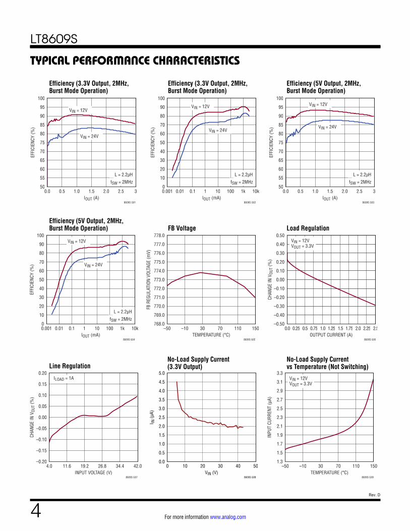
APPLICATIONS INFORMATIONAchieving Ultralow Quiescent Current
To enhance efficiency at light loads, the LT8609S enters into low ripple Burst Mode operation, which keeps the output capacitor charged to the desired output voltage while minimizing the input quiescent current and min-imizing output voltage ripple. In Burst Mode operation the LT8609S delivers single small pulses of current to the output capacitor followed by sleep periods where the output power is supplied by the output capacitor. While in sleep mode the LT8609S consumes 1.7μA.
As the output load decreases, the frequency of single cur-rent pulses decreases (see Figure 1) and the percentage of time the LT8609S is in sleep mode increases, result-ing in much higher light load efficiency than for typical converters. By maximizing the time between pulses, the
INPUT VOLTAGE (V)8609S F01b
0
LOAD
CUR
RENT
(mA)
100
40
60
20
80
90
30
50
10
70
030 5020 4010
VOUT = 5VfSW = 700kHzSYNC = FLOAT
Figure 1b. Full Switching Frequency Minimum Load vs VIN in Pulse Skipping Mode
Figure 2. Burst Mode Operation
2.00µs/DIV
200mA/DIV
10mV/DIV
8609S F02
converter quiescent current approaches 2.5µA for a typ-ical application when there is no output load. Therefore, to optimize the quiescent current performance at light loads, the current in the feedback resistor divider must be minimized as it appears to the output as load current.
While in Burst Mode operation the current limit of the top switch is approximately 600mA resulting in output voltage ripple shown in Figure 2. Increasing the output capacitance will decrease the output ripple proportionally. As load ramps upward from zero the switching frequency will increase but only up to the switching frequency programmed by the resistor at the RT pin as shown in Table 1. The output load at which the LT8609S reaches the programmed frequency varies based on input voltage, output voltage, and inductor choice.
For some applications it is desirable for the LT8609S to operate in pulse-skipping mode, offering two major differ-ences from Burst Mode operation. First is the clock stays awake at all times and all switching cycles are aligned to the clock. In this mode much of the internal circuitry is awake at all times, increasing quiescent current to several hundred µA. Second is that full switching frequency is reached at lower output load than in Burst Mode operation as shown in Figure 1b. To enable pulse-skipping mode the SYNC pin is floated. To achieve spread spectrum modula-tion with pulse-skipping mode, the SYNC pin is tied high. While a clock is applied to the SYNC pin the LT8609S will also operate in pulse-skipping mode.
LOAD CURRENT (mA)0
FREQ
UENC
Y (k
Hz)
2500
1000
1500
500
2000
0600200 400
L = 2.2µHVOUT = 3.3VVIN = 12VSYNC = 0V
8609S F01a
Figure 1a. SW Burst Mode Frequency vs Load
LT8609S
13Rev. D
For more information www.analog.com
APPLICATIONS INFORMATIONFB Resistor Network
The output voltage is programmed with a resistor divider between the output and the FB pin. Choose the resistor values according to:
R1=R2 VOUT
0.774V–1
⎛
⎝⎜
⎞
⎠⎟
1% resistors are recommended to maintain output voltage accuracy.
The total resistance of the FB resistor divider should be selected to be as large as possible when good low load efficiency is desired: The resistor divider generates a small load on the output, which should be minimized to optimize the quiescent current at low loads.
When using large FB resistors, a 10pF phase lead capac-itor should be connected from VOUT to FB.
Setting the Switching Frequency
The LT8609S uses a constant frequency PWM archi-tecture that can be programmed to switch from 200kHz to 2.2MHz by using a resistor tied from the RT pin to ground. A table showing the necessary RT value for a desired switching frequency is in Table 1. When in spread spectrum modulation mode, the frequency is modulated upwards of the frequency set by RT.
Table 1. SW Frequency vs RT ValuefSW (MHz) RT (kΩ)
0.2 2210.300 1430.400 1100.500 86.60.600 71.50.700 60.40.800 52.30.900 46.41.000 40.21.200 33.21.400 27.41.600 23.71.800 20.52.000 18.22.200 16.2
Operating Frequency Selection and Trade-Offs
Selection of the operating frequency is a trade-off between efficiency, component size, and input voltage range. The advantage of high frequency operation is that smaller inductor and capacitor values may be used. The disadvan-tages are lower efficiency and a smaller input voltage range.
The highest switching frequency (fSW(MAX)) for a given application can be calculated as follows:
fSW(MAX) =
VOUT +VSW(BOT)
tON(MIN) VIN – VSW(TOP)+VSW(BOT)( )where VIN is the typical input voltage, VOUT is the output voltage, VSW(TOP) and VSW(BOT) are the internal switch drops (~0.4V, ~0.25V, respectively at max load) and tON(MIN) is the minimum top switch on-time (see Electrical Characteristics). This equation shows that slower switch-ing frequency is necessary to accommodate a high VIN/VOUT ratio.
For transient operation VIN may go as high as the Abs Max rating regardless of the RT value, however the LT8609S will reduce switching frequency as necessary to maintain control of inductor current to assure safe operation.
The LT8609S is capable of maximum duty cycle approaching 100%, and the VIN to VOUT dropout is limited by the RDS(ON) of the top switch. In this mode the LT8609S skips switch cycles, resulting in a lower switching frequency than programmed by RT.
For applications that cannot allow deviation from the pro-grammed switching frequency at low VIN/VOUT ratios use the following formula to set switching frequency:
VIN(MIN) =
VOUT +VSW(BOT)
1– fSW • tOFF(MIN)– VSW(BOT)+VSW(TOP)
where VIN(MIN) is the minimum input voltage without skipped cycles, VOUT is the output voltage, VSW(TOP) and VSW(BOT) are the internal switch drops (~0.4V, ~0.25V, respectively at max load), fSW is the switching frequency (set by RT), and tOFF(MIN) is the minimum switch off-time. Note that higher switching frequency will increase the minimum input voltage below which cycles will be dropped to achieve higher duty cycle.
LT8609S
14Rev. D
For more information www.analog.com
APPLICATIONS INFORMATIONInductor Selection and Maximum Output Current
The LT8609S is designed to minimize solution size by allowing the inductor to be chosen based on the output load requirements of the application. During overload or short circuit conditions the LT8609S safely tolerates oper-ation with a saturated inductor through the use of a high speed peak-current mode architecture.
A good first choice for the inductor value is:
L=
VOUT +VSW(BOT)
fSWwhere fSW is the switching frequency in MHz, VOUT is the output voltage, VSW(BOT) is the bottom switch drop (~0.25V) and L is the inductor value in μH.
To avoid overheating and poor efficiency, an inductor must be chosen with an RMS current rating that is greater than the maximum expected output load of the applica-tion. In addition, the saturation current (typically labeled ISAT) rating of the inductor must be higher than the load current plus 1/2 of in inductor ripple current:
IL(PEAK) =ILOAD(MAX)+
12ΔL
where ∆IL is the inductor ripple current as calculated sev-eral paragraphs below and ILOAD(MAX) is the maximum output load for a given application.
As a quick example, an application requiring 1A output should use an inductor with an RMS rating of greater than 1A and an ISAT of greater than 1.3A. To keep the efficiency high, the series resistance (DCR) should be less than 0.04Ω, and the core material should be intended for high frequency applications.
The LT8609S limits the peak switch current in order to protect the switches and the system from overload faults. The top switch current limit (ILIM) is typically 4.75A at low duty cycles and decreases linearly to 4.0A at D = 0.8. The inductor value must then be sufficient to supply the desired maximum output current (IOUT(MAX)), which is a function of the switch current limit (ILIM) and the ripple current:
IOUT(MAX) =ILIM – ΔIL
2
The peak-to-peak ripple current in the inductor can be calculated as follows:
ΔIL =
VOUTL • fSW
1– VOUTVIN(MAX)
⎛
⎝⎜⎜
⎞
⎠⎟⎟
where fSW is the switching frequency of the LT8609S, and L is the value of the inductor. Therefore, the maximum out-put current that the LT8609S will deliver depends on the minimum switch current limit, the inductor value, and the input and output voltages. The inductor value may have to be increased if the inductor ripple current does not allow sufficient maximum output current (IOUT(MAX)) given the switching frequency, and maximum input voltage used in the desired application.
The optimum inductor for a given application may differ from the one indicated by this design guide. A larger value inductor provides a higher maximum load current and reduces the output voltage ripple. For applications requir-ing smaller load currents, the value of the inductor may be lower and the LT8609S may operate with higher ripple current. This allows use of a physically smaller inductor, or one with a lower DCR resulting in higher efficiency. Be aware that low inductance may result in discontinuous mode operation, which further reduces maximum load current.
The internal circuitry of the LT8609S is capable of sup-plying IOUT(MAX) up to 3A. Thermal limitations of the LT8609S prevent continuous output of 3A loads due to unsafe operating temperatures. In order to ensure safe operating temperature, the average LT8609S current must be kept below 2A, but will allow transient peaks up to 3A or IOUT(MAX). If high average currents cause unsafe heating of the part, the LT8609S will stop switching and indicate a fault condition to protect the internal circuitry.
For more information about maximum output current and discontinuous operation, see Analog Devices Application Note 44.
Finally, for duty cycles greater than 50% (VOUT/VIN > 0.5), a minimum inductance is required to avoid sub-harmonic oscillation. See Analog Devices Application Note 19.
https://www.analog.com/media/en/technical-documentation/application-notes/an44fa.pdf?doc=LT8609S.pdf
LT8609S
15Rev. D
For more information www.analog.com
APPLICATIONS INFORMATIONInput Capacitor
Bypass the input of the LT8609S circuit with a ceramic capacitor of X7R or X5R type. Y5V types have poor per-formance over temperature and applied voltage, and should not be used. A 4.7μF to 10μF ceramic capacitor is adequate to bypass the LT8609S and will easily handle the ripple current. Note that larger input capacitance is required when a lower switching frequency is used. If the input power source has high impedance, or there is sig-nificant inductance due to long wires or cables, additional bulk capacitance may be necessary. This can be provided with a low performance electrolytic capacitor.
Step-down regulators draw current from the input sup-ply in pulses with very fast rise and fall times. The input capacitor is required to reduce the resulting voltage rip-ple at the LT8609S and to force this very high frequency switching current into a tight local loop, minimizing EMI. A 4.7μF capacitor is capable of this task, but only if it is placed close to the LT8609S (see the PCB Layout sec-tion). A second precaution regarding the ceramic input capacitor concerns the maximum input voltage rating of the LT8609S. A ceramic input capacitor combined with trace or cable inductance forms a high quality (under damped) tank circuit. If the LT8609S circuit is plugged into a live supply, the input voltage can ring to twice its nominal value, possibly exceeding the LT8609S’s voltage rating. This situation is easily avoided (see Analog Devices Application Note 88).
Output Capacitor and Output Ripple
The output capacitor has two essential functions. Along with the inductor, it filters the square wave generated by the LT8609S to produce the DC output. In this role it determines the output ripple, thus low impedance at the switching frequency is important. The second function is to store energy in order to satisfy transient loads and stabilize the LT8609S’s control loop. Ceramic capacitors have very low equivalent series resistance (ESR) and pro-vide the best ripple performance. A good starting value is:
COUT =
100VOUT • fSW
where fSW is in MHz, and COUT is the recommended output capacitance in μF. Use X5R or X7R types. This choice will provide low output ripple and good transient response. Transient performance can be improved with a higher value output capacitor and the addition of a feedforward capacitor placed between VOUT and FB. Increasing the out-put capacitance will also decrease the output voltage rip-ple. A lower value of output capacitor can be used to save space and cost but transient performance will suffer and may cause loop instability. See the Typical Applications in this data sheet for suggested capacitor values.
When choosing a capacitor, special attention should be given to the data sheet to calculate the effective capaci-tance under the relevant operating conditions of voltage bias and temperature. A physically larger capacitor or one with a higher voltage rating may be required.
Ceramic Capacitors
Ceramic capacitors are small, robust and have very low ESR. However, ceramic capacitors can cause problems when used with the LT8609S due to their piezoelectric nature. When in Burst Mode operation, the LT8609S’s switching frequency depends on the load current, and at very light loads the LT8609S can excite the ceramic capacitor at audio frequencies, generating audible noise. Since the LT8609S operates at a lower current limit during Burst Mode operation, the noise is typically very quiet to a casual ear. If this is unacceptable, use a high performance tantalum or electrolytic capacitor at the output.
A final precaution regarding ceramic capacitors concerns the maximum input voltage rating of the LT8609S. As previously mentioned, a ceramic input capacitor com-bined with trace or cable inductance forms a high quality (under damped) tank circuit. If the LT8609S circuit is plugged into a live supply, the input voltage can ring to twice its nominal value, possibly exceeding the LT8609S’s rating. This situation is easily avoided (see Analog Devices Application Note 88).
Enable Pin
The LT8609S is in shutdown when the EN pin is low and active when the pin is high. The rising threshold of the EN comparator is 1.05V, with 50mV of hysteresis. The EN pin
LT8609S
16Rev. D
For more information www.analog.com
can be tied to VIN if the shutdown feature is not used, or tied to a logic level if shutdown control is required.
Adding a resistor divider from VIN to EN programs the LT8609S to regulate the output only when VIN is above a desired voltage (see Block Diagram). Typically, this threshold, VIN(EN), is used in situations where the input supply is current limited, or has a relatively high source resistance. A switching regulator draws constant power from the source, so source current increases as source voltage drops. This looks like a negative resistance load to the source and can cause the source to current limit or latch low under low source voltage conditions. The VIN(EN) threshold prevents the regulator from operating at source voltages where the problems might occur. This threshold can be adjusted by setting the values R3 and R4 such that they satisfy the following equation:
VIN(EN) =
R3R4
+1⎛
⎝⎜
⎞
⎠⎟•1V
where the LT8609S will remain off until VIN is above VIN(EN). Due to the comparator’s hysteresis, switching will not stop until the input falls slightly below VIN(EN).
When in Burst Mode operation for light-load currents, the current through the VIN(EN) resistor network can eas-ily be greater than the supply current consumed by the LT8609S. Therefore, the VIN(EN) resistors should be large to minimize their effect on efficiency at low loads.
INTVCC Regulator
An internal low dropout (LDO) regulator produces the 3.5V supply from VIN that powers the drivers and the internal bias circuitry. The INTVCC can supply enough current for the LT8609S’s circuitry and must be bypassed to ground with a minimum of 1μF ceramic capacitor. Good bypass-ing is necessary to supply the high transient currents required by the power MOSFET gate drivers. Applications with high input voltage and high switching frequency will increase die temperature because of the higher power dissipation across the LDO. Do not connect an external load to the INTVCC pin.
APPLICATIONS INFORMATIONOutput Voltage Tracking and Soft-Start
The LT8609S allows the user to program its output voltage ramp rate by means of the TR/SS pin. An internal 2μA pulls up the TR/SS pin to INTVCC. Putting an external capacitor on TR/SS enables soft-starting the output to prevent current surge on the input supply. During the soft-start ramp the output voltage will proportionally track the TR/SS pin voltage. For output tracking applications, TR/SS can be externally driven by another voltage source. From 0V to 0.774V, the TR/SS voltage will override the internal 0.774V reference input to the error amplifier, thus regulating the FB pin voltage to that of TR/SS pin. When TR/SS is above 0.774V, tracking is disabled and the feed-back voltage will regulate to the internal reference voltage.
An active pull-down circuit is connected to the TR/SS pin which will discharge the external soft-start capacitor in the case of fault conditions and restart the ramp when the faults are cleared. Fault conditions that clear the soft-start capacitor are the EN/UV pin transitioning low, VIN voltage falling too low, or thermal shutdown.
Output Power Good
When the LT8609S’s output voltage is within the ±8.5% window of the regulation point, which is a VFB voltage in the range of 0.716V to 0.849V (typical), the output voltage is considered good and the open-drain PG pin goes high impedance and is typically pulled high with an external resistor. Otherwise, the internal drain pull-down device will pull the PG pin low. To prevent glitching both the upper and lower thresholds include 0.5% of hysteresis.
The PG pin is also actively pulled low during several fault conditions: EN/UV pin is below 1V, INTVCC has fallen too low, VIN is too low, or thermal shutdown.
Synchronization
To select low ripple Burst Mode operation, tie the SYNC pin below 0.4V (this can be ground or a logic low output). To synchronize the LT8609S oscillator to an external fre-quency connect a square wave (with 20% to 80% duty cycle) to the SYNC pin. The square wave amplitude should have valleys that are below 0.9V and peaks above 2.7V (up to 5V).

LT8609S
17Rev. D
For more information www.analog.com
APPLICATIONS INFORMATIONThe LT8609S will not enter Burst Mode operation at low output loads while synchronized to an external clock, but instead will pulse skip to maintain regulation. The LT8609S may be synchronized over a 200kHz to 2.2MHz range. The RT resistor should be chosen to set the LT8609S switching frequency equal to or below the low-est synchronization input. For example, if the synchro-nization signal will be 500kHz and higher, the RT should be selected for 500kHz. The slope compensation is set by the RT value, while the minimum slope compensation required to avoid subharmonic oscillations is established by the inductor size, input voltage, and output voltage. Since the synchronization frequency will not change the slopes of the inductor current waveform, if the inductor is large enough to avoid subharmonic oscillations at the frequency set by RT, then the slope compensation will be sufficient for all synchronization frequencies.
For some applications it is desirable for the LT8609S to operate in pulse-skipping mode, offering two major differ-ences from Burst Mode operation. First is the clock stays awake at all times and all switching cycles are aligned to the clock. Second is that full switching frequency is reached at lower output load than in Burst Mode operation as shown in Figure 1b in an earlier section. These two differences come at the expense of increased quiescent current. To enable pulse-skipping mode the SYNC pin is floated.
For some applications, reduced EMI operation may be desirable, which can be achieved through spread spec-trum modulation. This mode operates similar to pulse skipping mode operation, with the key difference that the switching frequency is modulated up and down by a 3 kHz triangle wave. The modulation has the frequency set by RT as the low frequency, and modulates up to approximately 20% higher than the frequency set by RT. To enable spread spectrum mode, tie SYNC to INTVCC or drive to a voltage between 3.2V and 5V.
The LT8609S does not operate in forced continuous mode regardless of SYNC signal.
Shorted and Reversed Input Protection
The LT8609S will tolerate a shorted output. Several fea-tures are used for protection during output short-circuit
and brownout conditions. The first is the switching fre-quency will be folded back while the output is lower than the set point to maintain inductor current control (only if SYNC = 0V).. Second, the bottom switch current is mon-itored such that if inductor current is beyond safe levels switching of the top switch will be delayed until such time as the inductor current falls to safe levels. This allows for tailoring the LT8609S to individual applications and lim-iting thermal dissipation during short circuit conditions.
Frequency foldback behavior depends on the state of the SYNC pin: If the SYNC pin is low or high, or floated the switching frequency will slow while the output voltage is lower than the programmed level. If the SYNC pin is connected to a clock source, the LT8609S will stay at the programmed frequency without foldback and only slow switching if the inductor current exceeds safe levels.
There is another situation to consider in systems where the output will be held high when the input to the LT8609S is absent. This may occur in battery charging applications or in battery backup systems where a battery or some other supply is diode ORed with the LT8609S’s output. If the VIN pin is allowed to float and the EN pin is held high (either by a logic signal or because it is tied to VIN), then the LT8609S’s internal circuitry will pull its quies-cent current through its SW pin. This is acceptable if the system can tolerate several μA in this state. If the EN pin is grounded the SW pin current will drop to near 0.7µA. However, if the VIN pin is grounded while the output is held high, regardless of EN, parasitic body diodes inside the LT8609S can pull current from the output through the SW pin and the VIN pin. Figure 3 shows a connection of the VIN and EN/UV pins that will allow the LT8609S to run only when the input voltage is present and that protects against a shorted or reversed input.
Figure 3.
VINVIN
LT8609S
GND
D1
8609S F03
EN/UV
Reverse VIN Protection

LT8609S
18Rev. D
For more information www.analog.com
APPLICATIONS INFORMATIONside of the circuit board, and their connections should be made on that layer. Place a local, unbroken ground plane under the application circuit on the layer closest to the surface layer. The SW node should be as small as possible. Finally, keep the FB and RT nodes small so that the ground traces will shield them from the SW node. The exposed pad on the bottom of the package must be soldered to ground so that the pad is connected to ground electrically and also acts as a heat sink thermally. To keep thermal resistance low, extend the ground plane as much as possible, and add thermal vias under and near the LT8609S to additional ground planes within the circuit board and on the bottom side. For mechani-cal performance during temperature cycles, solder the corner N/C pins to the ground plane.
PCB Layout
For proper operation and minimum EMI, care must be taken during printed circuit board layout. Figure 4 shows the recommended component placement with trace, ground plane and via locations. Note that large, switched currents flow in the LT8609S’s VIN pins, GND pins, and the input capacitor (CIN). The loop formed by the input capacitor should be as small as possible by placing the capacitor adjacent to the VIN and GND pins. When using a physically large input capacitor the resulting loop may become too large in which case using a small case/value capacitor placed close to the VIN and GND pins plus a larger capacitor further away is preferred. These components, along with the induc-tor and output capacitor, should be placed on the same
Figure 4. PCB Layout
8609S F04GND VIA VIN VIA VOUT VIA OTHER SIGNAL VIA
COUT
CVCC
L
RT R2 CFF
R1
CSS
RPG
CIN
R4
R3
GROUND PLANE ON LAYER 2
1
LT8609S
19Rev. D
For more information www.analog.com
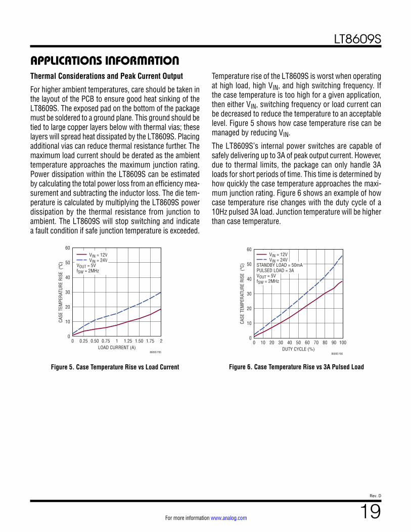
Thermal Considerations and Peak Current Output
For higher ambient temperatures, care should be taken in the layout of the PCB to ensure good heat sinking of the LT8609S. The exposed pad on the bottom of the package must be soldered to a ground plane. This ground should be tied to large copper layers below with thermal vias; these layers will spread heat dissipated by the LT8609S. Placing additional vias can reduce thermal resistance further. The maximum load current should be derated as the ambient temperature approaches the maximum junction rating. Power dissipation within the LT8609S can be estimated by calculating the total power loss from an efficiency mea-surement and subtracting the inductor loss. The die tem-perature is calculated by multiplying the LT8609S power dissipation by the thermal resistance from junction to ambient. The LT8609S will stop switching and indicate a fault condition if safe junction temperature is exceeded.
Temperature rise of the LT8609S is worst when operating at high load, high VIN, and high switching frequency. If the case temperature is too high for a given application, then either VIN, switching frequency or load current can be decreased to reduce the temperature to an acceptable level. Figure 5 shows how case temperature rise can be managed by reducing VIN.
The LT8609S’s internal power switches are capable of safely delivering up to 3A of peak output current. However, due to thermal limits, the package can only handle 3A loads for short periods of time. This time is determined by how quickly the case temperature approaches the maxi-mum junction rating. Figure 6 shows an example of how case temperature rise changes with the duty cycle of a 10Hz pulsed 3A load. Junction temperature will be higher than case temperature.
APPLICATIONS INFORMATION
Figure 5. Case Temperature Rise vs Load Current Figure 6. Case Temperature Rise vs 3A Pulsed Load
LOAD CURRENT (A)0 0.25 0.50 0.75 1 1.25 1.50 1.75 2
0
10
20
30
40
50
60
CASE
TEM
PERA
TURE
RIS
E (°
C)
8609S F05
VIN = 12VVIN = 24V
VOUT = 5VfSW = 2MHz
DUTY CYCLE (%)0 10 20 30 40 50 60 70 80 90 100
0
10
20
30
40
50
60
CASE
TEM
PERA
TURE
RIS
E (°
C)
8609S F06
VIN = 12VVIN = 24V
STANDBY LOAD = 50mAPULSED LOAD = 3AVOUT = 5VfSW = 2MHz

LT8609S
20Rev. D
For more information www.analog.com
TYPICAL APPLICATIONS3.3V Step Down
5V Step Down
12V Step Down
C24.7µF
C31µF
C510pF
L12.2µH
R118.2k
R21MR3
309k
R4100k
C610nF
VIN
EN/UV
SYNC
LT8609SINTVCC
TR/SS
RTGND
FB
PG
SW
VIN3.8V
TO 42V
POWER GOOD
fSW = 2MHz L1 = XFL4020-222ME
VOUT3.3V2A
8609S TA02
C422µFX7R1206
C24.7µF
C31µF
C510pF
L12.2µH
R118.2k
R21MR3
182k
R4100k
C610nF
VIN
EN/UV
SYNC
LT8609SINTVCC
TR/SS
RTGND
FB
PG
SW
VIN5V
TO 42V
POWER GOOD
fSW = 2MHz L1 = XFL4020-222ME
VOUT5V2A
8609S TA03
C422µFX7R1206
C24.7µF
C31µF
C422µFX7R1206
C510pF
L110µH
R140.2k
R21MR3
69.8k
R4100k
C610nF
VIN
EN/UV
SYNC
LT8609SINTVCC
TR/SS
RTGND
FB
PG
SW
VIN12.5V
TO 42V
POWER GOOD
FSW = 1MHz L1 = XAL4040-103ME
VOUT12V2A
8609S TA04
LT8609S
21Rev. D
For more information www.analog.com
TYPICAL APPLICATIONS1.8V 2MHz Step-Down Converter
Ultralow EMI 3.3V 2A Step-Down Converter
C24.7µF
C31µF
C510pF
L12.2µH
R118.2k
R21MR3
768k
R4100k
C610nF
VIN
EN/UV
SYNC
LT8609S
INTVCC
TR/SS
RTGND
FB
PG
SW
VIN3.1V
TO 20V(42V TRANSIENT)
POWER GOOD
fSW = 2MHz L1 = XFL4020-222ME
VOUT1.8V2A
8609S TA05
PSKIP M1NFET C4
47µFX7R1210
C24.7µF
C31µF
C510pF
L18.2µH
R1110k
R21MR3
309k
R4100K
C610nF
L2BEAD
L34.7µH
C74.7µF
C84.7µF
VIN
EN/UV
SYNC
LT8609S
INTVCC
TR/SS
RT
GND
FB
PG
SW
VIN4V TO 40V
POWER GOOD
fSW = 400kHz L1 = XAL4040-822C9 = OS-CON 63SXV33ML3 = XAL4030-472
VOUT3.3V2A
8609S TA06
C447µFX7R1210
C933µF

LT8609S
22Rev. D
For more information www.analog.com
PACKAGE DESCRIPTION
LQFN
Pac
kage
16-L
ead
(3m
m ×
3m
m ×
0.9
4mm
)(R
efer
ence
LTC
DW
G #
05-0
8-15
16 R
ev B
)
DETA
IL B
A
PACK
AGE
TOP
VIEW
5
PAD
“A1”
CORN
ER
Y
X
aaa
Z2×
16b
PACK
AGE
BOTT
OM V
IEW
4
6
SEE
NOTE
SE
D
b
0.37
5e
e
bE1
D1
DETA
IL B
SUBS
TRAT
EM
OLD
CAP
// bbb Z
Z
H2H1DE
TAIL
C
SUGG
ESTE
D PC
B LA
YOUT
TOP
VIEW0.0000
0.00
00
0.75
00
0.25
00
0.25
00
0.75
00
0.7500
0.2500
0.2500
0.7500
DETA
IL A
7
SEE
NOTE
S
PIN
1 NO
TCH
0.25
× 4
5°
1316
85
1 4
12 9
aaa Z 2×M
XY
Zcc
c
MXY Z ccc
MX
YZ
eee
MZ
fff
PACK
AGE
OUTL
INE
0.25
±0.
05
0.70
±0.
05
3.50
±0.
05
3.50
±0.
05
LGA
16 0
317
REV
B
TRAY
PIN
1BE
VEL
PACK
AGE
IN T
RAY
LOAD
ING
ORIE
NTAT
ION
COM
PONE
NTPI
N “A
1”
LTXX
XXX
0.37
50.
375
DETA
IL A
ddd Z16×
SYM
BOL
A A1 L b D E D1 E1 e H1 H2 aaa
bbb
ccc
ddd
eee
fff
MIN
0.85
0.01
0.30
0.22
NOM
0.94
0.02
0.40
0.25
3.00
3.00
1.45
1.45
0.50
0.24
0.70
MAX
1.03
0.03
0.50
0.28
0.10
0.10
0.10
0.10
0.15
0.08
NOTE
S
DIM
ENSI
ONS
Z
A1 DETA
IL C
NOTE
S:1.
DIM
ENSI
ONIN
G AN
D TO
LERA
NCIN
G PE
R AS
ME
Y14.
5M-1
994
2. A
LL D
IMEN
SION
S AR
E IN
MIL
LIM
ETER
S
3. P
RIM
ARY
DATU
M -Z
- IS
SEAT
ING
PLAN
E
MET
AL F
EATU
RES
UNDE
R TH
E SO
LDER
MAS
K OP
ENIN
G NO
T SH
OWN
SO
AS
NOT
TO O
BSCU
RE T
HESE
TER
MIN
ALS
AND
HEAT
FEA
TURE
S
54
DETA
ILS
OF P
AD #
1 ID
ENTI
FIER
ARE
OPT
IONA
L, B
UT M
UST
BE
LOCA
TED
WIT
HIN
THE
ZONE
INDI
CATE
D. T
HE P
AD #
1 ID
ENTI
FIER
M
AY B
E EI
THER
A M
OLD
OR M
ARKE
D FE
ATUR
E
6TH
E EX
POSE
D HE
AT F
EATU
RE M
AY H
AVE
OPTI
ONAL
COR
NER
RADI
I
7CO
RNER
SUP
PORT
PAD
CHA
MFE
R IS
OPT
IONA
L
e
L
e/2
1.45
1.45
0.37
5
0.37
5
LT8609S
23Rev. D
For more information www.analog.com
Information furnished by Analog Devices is believed to be accurate and reliable. However, no responsibility is assumed by Analog Devices for its use, nor for any infringements of patents or other rights of third parties that may result from its use. Specifications subject to change without notice. No license is granted by implication or otherwise under any patent or patent rights of Analog Devices.
REVISION HISTORYREV DATE DESCRIPTION PAGE NUMBER
A 10/17 Clarified Oscillator Frequency RT ConditionsClarified Frequency Foldback GraphClarified Block DiagramClarified Operating Frequency Selection in Applications InformationClarified PCB Layout in Figure 4Clarified Figure 5 and 6
36
11141819
B 04/20 Updated θJA in Pin Configuration DiagramAdded Note 4Update Electrical Characteristics table Minimum On-Time parameter with ILOAD from 1.5A to 1.75A
233
C 10/20 Added AEC-Q statement and #W ordering information 1, 2
D 02/21 Added Tape and Reel in the Order Information table 2

LT8609S
24Rev. D
For more information www.analog.comwww.analog.com
ANALOG DEVICES, INC. 2017-2021
02/21
RELATED PARTS
TYPICAL APPLICATION
PART NUMBER DESCRIPTION COMMENTS
LT8606 42V, 350mA, 92% Efficiency, 2.2MHz Synchronous Step-Down DC/DC Converter
VIN = 3.0V to 42V, VOUT(MIN) = 0.778V, IQ = 3µA, ISD < 1µA, MSOP-10E and 2mm × 2mm DFN-8 Packages
LT8607 42V, 750mA, 93% Efficiency, 2.2MHz Synchronous Step-Down DC/DC Converter
VIN = 3.0V to 42V, VOUT(MIN) = 0.778V, IQ = 3µA, ISD < 1µA, MSOP-10E and 2mm × 2mm DFN-8 Packages
LT8609/LT8609A/LT8609B
42V, 2A, 94% Efficiency, 2.2MHz Synchronous MicroPower Step-Down DC/DC Converter with IQ = 2.5µA
VIN = 3V to 42V, VOUT(MIN) = 0.8V, IQ = 2.5µA, ISD < 1µA, MSOP-10E Package
LT8640S 42V, 6A, 95% Efficiency, 2.2MHz Synchronous Silent Switcher 2 Step-Down DC/DC Converter with IQ = 2.5µA
VIN = 3.4V to 42V, VOUT(MIN) = 0.97V, IQ = 2.5µA, ISD < 1µA, 4mm × 4mm LQFN-24 Package
LT8645S 65V, 8A, 95% Efficiency, 2.2MHz Synchronous Silent Switcher 2 Step-Down DC/DC Converter with IQ = 2.5µA
VIN = 3.4V to 65V, VOUT(MIN) = 0.8V, IQ = 2.5µA, ISD < 1µA, 4mm × 6mm LQFN-32 Package
LT8640 42V, 5A, 95% Efficiency, 2.2MHz Synchronous Silent Switcher 2 Step-Down DC/DC Converter with IQ = 2.5µA
VIN = 3.4V to 42V, VOUT(MIN) = 0.97V, IQ = 2.5µA, ISD < 1µA, 3mm × 4mm QFN-16 Package
LT8610A/ LT8610AB
42V, 3.5A, 96% Efficiency, 2.2MHz Synchronous MicroPower Step-Down DC/DC Converter with IQ = 2.5µA
VIN = 3.4V to 42V, VOUT(MIN) = 0.97V, IQ = 2.5µA, ISD < 1µA, MSOP-16E Package
LT8610AC 42V, 3.5A, 96% Efficiency, 2.2MHz Synchronous MicroPower Step-Down DC/DC Converter with IQ = 2.5µA
VIN = 3V to 42V, VOUT(MIN) = 0.8V, IQ = 2.5µA, ISD < 1µA, MSOP-16E Package
LT8610 42V, 2.5A, 96% Efficiency, 2.2MHz Synchronous MicroPower Step-Down DC/DC Converter with IQ = 2.5µA
VIN = 3.4V to 42V, VOUT(MIN) = 0.97V, IQ = 2.5µA, ISD < 1µA, MSOP-16E Package
LT8612 42V, 6A, 96% Efficiency, 2.2MHz Synchronous MicroPower Step-Down DC/DC Converter with IQ = 2.5µA
VIN = 3.4V to 42V, VOUT(MIN) = 0.97V, IQ = 3.0µA, ISD < 1µA, 3mm × 6mm QFN-28 Package
LT8602 42V, Quad Output (2.5A+1.5A+1.5A+1.5A) 95% Efficiency, 2.2MHz Synchronous MicroPower Step-Down DC/DC Converter with IQ = 25µA
VIN = 3V to 42V, VOUT(MIN)= 0.8V, IQ = 25µA, ISD < 1µA, 6mm × 6mm QFN-40 Package
C84.7µFR9
10k
R1031.6k C10
47µF
C1110pF
L22.2µH
R518.2k
R61MR7
768k
R8100k
C121µF
VINEN/UV
SYNCLT8609S
INTVCC
TR/SS
RTGND
FB
PG
SW
POWER GOOD
fSW = 2MHz
VOUT1.8V2A
8609S TA07
C24.7µF
C31µF
C447µF
C510pF
L12.2µH
R118.2k
R21MR3
309k
R4100k
C610nF
VINEN/UV
LT8609S
INTVCC
TR/SS
RTGND
FB
PG
SW
VIN3.8V
TO 20V(42V TRANSIENT)
POWER GOOD
fSW = 2MHz
VOUT3.3V, 2A
SYNC
L1, L2 = XFL4020-222MEC2,C8 = X7R 1206C4, C10 = X7R 1210
Tracking 3.3V and 1.8V 2MHz Converters

Mouser Electronics
Authorized Distributor
Click to View Pricing, Inventory, Delivery & Lifecycle Information: Analog Devices Inc.:
LT8609SIV#PBF LT8609SEV#PBF DC2522A LT8609SEV#TRPBF LT8609SIV#TRPBF SCP-LT8609S-BEVALZ
SCP-LT8609S-IEVALZ
Related Documents