LT6110 1 6110fa For more information www.linear.com/LT6110 TYPICAL APPLICATION FEATURES DESCRIPTION Cable/Wire Drop Compensator The LT ® 6110 is a precision high side current sense with a current mode output, designed for controlling the output voltage of an adjustable power supply or voltage regulator. This can be used to compensate for drops in voltage at a remote load due to resistance in a wire, trace or cable. The LT6110 monitors load current via a series-connected internal or external sense resistor. Two current mode out- puts, one sinking and one sourcing, are provided that are proportional to the load current. This allows the LT6110 to adjust the output voltage of a wide variety of regulators. Either output may be used to monitor the load current. Low DC offset allows for the use of a small sense resis- tor, as well as precise control of small variations in wire voltage drop. L, LT, LTC, LTM, Linear Technology, the Linear logo and µModule are registered trademarks and ThinSOT is a trademark of Linear Technology Corporation. All other trademarks are the property of their respective owners. APPLICATIONS n Improve Voltage Regulation to a Remote Load by 10× n Ideal for Resistor-Adjustable Voltage Regulators n Gain Configurable with a Single Resistor n High Side Current Sensing: Integrated 20mΩ Sense Resistor for Up to 3A Ability to Use an External Sense Resistor n 300µV Maximum Input Offset Voltage n Output Current Accuracy of 1% Maximum n 30µA Maximum Supply Current n 2V to 50V Supply Range n Fully Specified from –40°C to 125°C n Available in Low Profile (1mm) ThinSOT™ and (2mm × 2mm) DFN Packages n Automotive and Industrial Power Distribution n USB Power n DC/DC Converters n Plug-In DC Adapters n Power over Ethernet IOUT +IN –IN R IN LT6110 V + V – RS IMON + – V IN V REG I LOAD R WIRE V LOAD 6110 TA01 500mV/DIV 5V 5V 2A 1A V LOAD COMPENSATED V LOAD UNCOMPENSATED I LOAD 200μs/DIV OUT FB REGULATOR GND IN REMOTE LOAD

Welcome message from author
This document is posted to help you gain knowledge. Please leave a comment to let me know what you think about it! Share it to your friends and learn new things together.
Transcript

LT6110
16110fa
For more information www.linear.com/LT6110
Typical applicaTion
FeaTures DescripTion
Cable/Wire Drop Compensator
The LT®6110 is a precision high side current sense with a current mode output, designed for controlling the output voltage of an adjustable power supply or voltage regulator. This can be used to compensate for drops in voltage at a remote load due to resistance in a wire, trace or cable.
The LT6110 monitors load current via a series-connected internal or external sense resistor. Two current mode out-puts, one sinking and one sourcing, are provided that are proportional to the load current. This allows the LT6110 to adjust the output voltage of a wide variety of regulators. Either output may be used to monitor the load current.
Low DC offset allows for the use of a small sense resis-tor, as well as precise control of small variations in wire voltage drop.L, LT, LTC, LTM, Linear Technology, the Linear logo and µModule are registered trademarks and ThinSOT is a trademark of Linear Technology Corporation. All other trademarks are the property of their respective owners.
applicaTions
n Improve Voltage Regulation to a Remote Load by 10×n Ideal for Resistor-Adjustable Voltage Regulatorsn Gain Configurable with a Single Resistorn High Side Current Sensing:
Integrated 20mΩ Sense Resistor for Up to 3A Ability to Use an External Sense Resistor
n 300µV Maximum Input Offset Voltagen Output Current Accuracy of 1% Maximumn 30µA Maximum Supply Currentn 2V to 50V Supply Range n Fully Specified from –40°C to 125°Cn Available in Low Profile (1mm) ThinSOT™ and
(2mm × 2mm) DFN Packages
n Automotive and Industrial Power Distributionn USB Powern DC/DC Convertersn Plug-In DC Adaptersn Power over Ethernet
IOUT
+IN –IN
RIN
LT6110
V+
V–
RS
IMON
+ –
VINVREG ILOAD
RWIRE VLOAD
6110 TA01
500m
V/DI
V
5V
5V
2A
1A
VLOAD COMPENSATED
VLOAD UNCOMPENSATED
ILOAD
200µs/DIV
OUT
FB
REGULATOR
GND
IN
REMOTELOAD
LT6110
26110fa
For more information www.linear.com/LT6110
pin conFiguraTion
absoluTe MaxiMuM raTingsTotal Supply Voltage (V+ to V–) .................................55V+IN, –IN, IOUT, IMON to V– Voltage ............................ V+
+IN, -IN, IOUT, IMON Current .................................10mAIOUT to IMON Voltage ....................................36V, –0.6VV+, +IN to IOUT Voltage .............................................36VDifferential Input Voltage ............................................ V+
RSENSE Current (Note 2) Continuous .............................................................3A Transient (<0.1 Second) ..........................................5A
(Note 1)
NC* 1IOUT 2
IMON 3 V– 4
8 +IN7 V+
6 RS5 –IN
TOP VIEW
TS8 PACKAGE8-LEAD PLASTIC TSOT-23
TJMAX = 150°C, θJA = 195°C/W *NC PIN NOT INTERNALLY CONNECTED
TOP VIEW
+IN
V+
RS
–IN
NC*
IOUT
IMON
V–
DC PACKAGE8-LEAD (2mm × 2mm) PLASTIC DFN
9V–
4
1
2
3 6
5
7
8
TJMAX = 150°C, θJA = 80.6°C/W
EXPOSED PAD (PIN 9) IS V–, MUST BE SOLDERED TO PCB *NC PIN NOT INTERNALLY CONNECTED
orDer inForMaTion
Specified Temperature Range (Note 3) LT6110I ................................................–40°C to 85°C LT6110H ............................................. –40°C to 125°C
Junction Temperature .......................................... 150°CStorage Temperature Range .................. –65°C to 150°CLead Temperature (Soldering, 10 sec)
TS8 ................................................................... 300°C
Lead Free FinishTAPE AND REEL (MINI) TAPE AND REEL PART MARKING* PACKAGE DESCRIPTION SPECIFIED TEMPERATURE RANGE
LT6110ITS8#TRMPBF LT6110ITS8#TRPBF LTGCQ 8-Lead Plastic TSOT-23 –40°C to 85°C
LT6110HTS8#TRMPBF LT6110HTS8#TRPBF LTGCQ 8-Lead Plastic TSOT-23 –40°C to 125°C
LT6110IDC#TRMPBF LT6110IDC#TRPBF LGCP 8-Lead (2mm × 2mm) Plastic DFN –40°C to 85°C
LT6110HDC#TRMPBF LT6110HDC#TRPBF LGCP 8-Lead (2mm × 2mm) Plastic DFN –40°C to 125°CTRM = 500 pieces. *Temperature grades are identified by a label on the shipping container.Consult LTC Marketing for parts specified with wider operating temperature ranges. *The temperature grade is identified by a label on the shipping container. Consult LTC Marketing for information on lead based finish parts.For more information on lead free part marking, go to: http://www.linear.com/leadfree/ For more information on tape and reel specifications, go to: http://www.linear.com/tapeandreel/
LT6110
36110fa
For more information www.linear.com/LT6110
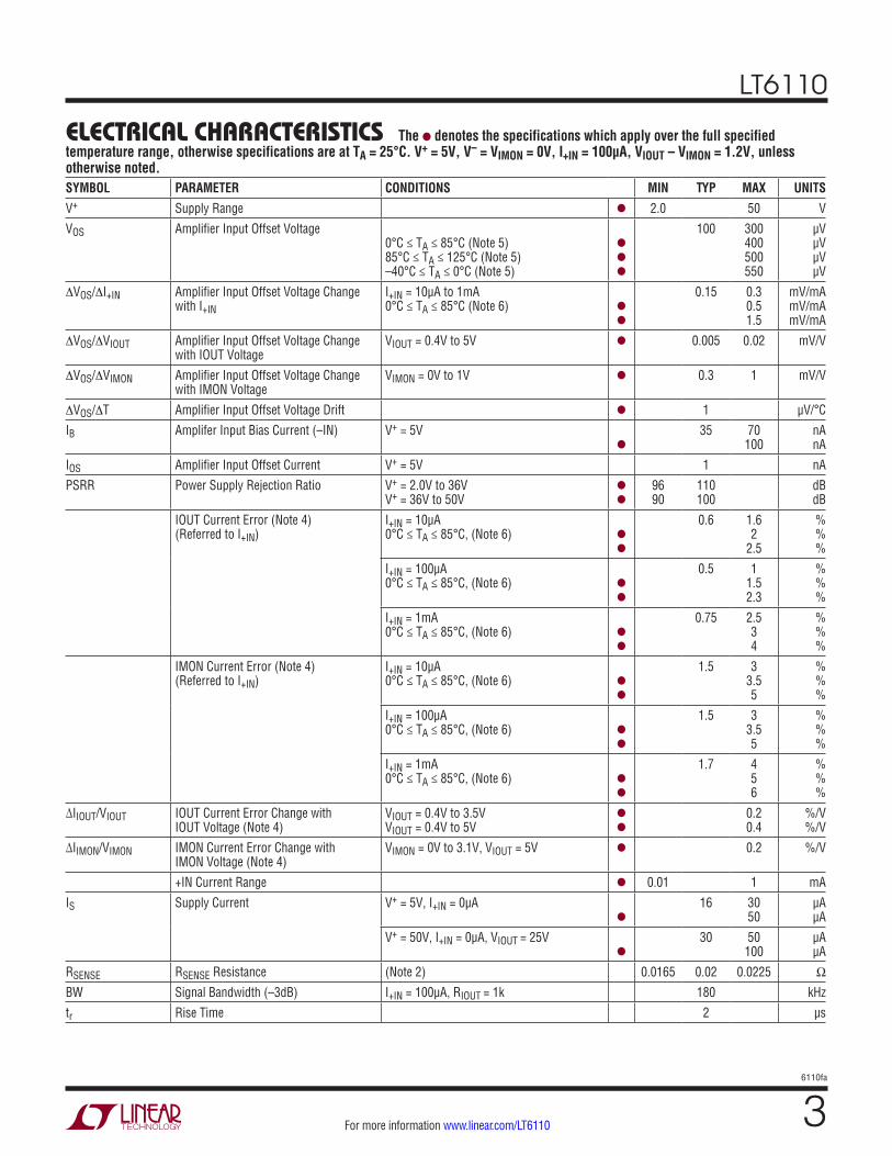
The l denotes the specifications which apply over the full specified temperature range, otherwise specifications are at TA = 25°C. V+ = 5V, V– = VIMON = 0V, I+IN = 100µA, VIOUT – VIMON = 1.2V, unless otherwise noted.
elecTrical characTerisTics
SYMBOL PARAMETER CONDITIONS MIN TYP MAX UNITSV+ Supply Range l 2.0 50 V
VOS Amplifier Input Offset Voltage 0°C ≤ TA ≤ 85°C (Note 5) 85°C ≤ TA ≤ 125°C (Note 5) –40°C ≤ TA ≤ 0°C (Note 5)
l
l
l
100 300 400 500 550
µV µV µV µV
∆VOS/∆I+IN Amplifier Input Offset Voltage Change with I+IN
I+IN = 10µA to 1mA 0°C ≤ TA ≤ 85°C (Note 6)
l
l
0.15 0.3 0.5 1.5
mV/mA mV/mA mV/mA
∆VOS/∆VIOUT Amplifier Input Offset Voltage Change with IOUT Voltage
VIOUT = 0.4V to 5V l 0.005 0.02 mV/V
∆VOS/∆VIMON Amplifier Input Offset Voltage Change with IMON Voltage
VIMON = 0V to 1V l 0.3 1 mV/V
∆VOS/∆T Amplifier Input Offset Voltage Drift l 1 µV/°C
IB Amplifer Input Bias Current (–IN) V+ = 5V
l
35 70 100
nA nA
IOS Amplifier Input Offset Current V+ = 5V 1 nA
PSRR Power Supply Rejection Ratio V+ = 2.0V to 36V V+ = 36V to 50V
l
l
96 90
110 100
dB dB
IOUT Current Error (Note 4) (Referred to I+IN)
I+IN = 10µA 0°C ≤ TA ≤ 85°C, (Note 6)
l
l
0.6 1.6 2
2.5
% % %
I+IN = 100µA 0°C ≤ TA ≤ 85°C, (Note 6)
l
l
0.5 1 1.5 2.3
% % %
I+IN = 1mA 0°C ≤ TA ≤ 85°C, (Note 6)
l
l
0.75 2.5 3 4
% % %
IMON Current Error (Note 4) (Referred to I+IN)
I+IN = 10µA 0°C ≤ TA ≤ 85°C, (Note 6)
l
l
1.5 3 3.5 5
% % %
I+IN = 100µA 0°C ≤ TA ≤ 85°C, (Note 6)
l
l
1.5 3 3.5 5
% % %
I+IN = 1mA 0°C ≤ TA ≤ 85°C, (Note 6)
l
l
1.7 4 5 6
% % %
∆IIOUT/VIOUT IOUT Current Error Change with IOUT Voltage (Note 4)
VIOUT = 0.4V to 3.5V VIOUT = 0.4V to 5V
l
l
0.2 0.4
%/V %/V
∆IIMON/VIMON IMON Current Error Change with IMON Voltage (Note 4)
VIMON = 0V to 3.1V, VIOUT = 5V l 0.2 %/V
+IN Current Range l 0.01 1 mA
IS Supply Current V+ = 5V, I+IN = 0µA
l
16 30 50
µA µA
V+ = 50V, I+IN = 0µA, VIOUT = 25V
l
30 50 100
µA µA
RSENSE RSENSE Resistance (Note 2) 0.0165 0.02 0.0225 Ω
BW Signal Bandwidth (–3dB) I+IN = 100µA, RIOUT = 1k 180 kHz
tr Rise Time 2 µs
LT6110
46110fa
For more information www.linear.com/LT6110
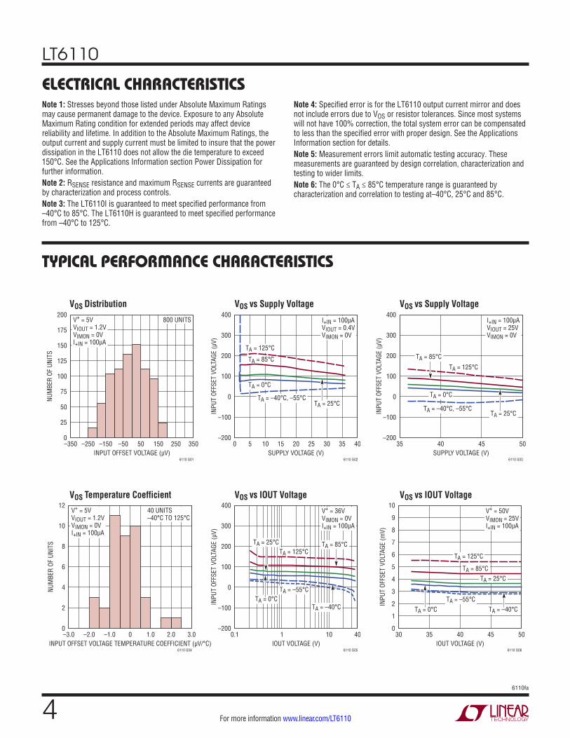
Typical perForMance characTerisTics
VOS Temperature Coefficient VOS vs IOUT Voltage VOS vs IOUT Voltage
VOS Distribution VOS vs Supply Voltage VOS vs Supply Voltage
SUPPLY VOLTAGE (V)0
INPU
T OF
FSET
VOL
TAGE
(µV)
400
300
200
0
100
–100
–20010 205 15 30
6110 G02
4025 35
TA = 0°C
TA = 25°C
TA = 85°C
TA = 125°C
TA = –40°C, –55°C
I+IN = 100µAVIOUT = 0.4VVIMON = 0V
SUPPLY VOLTAGE (V)35
INPU
T OF
FSET
VOL
TAGE
(µV)
400
300
200
0
100
–100
–20040
6110 G03
5045
TA = 25°C
TA = 0°C
TA = 125°C
TA = –40°C, –55°C
I+IN = 100µAVIOUT = 25VVIMON = 0V
TA = 85°C
IOUT VOLTAGE (V)0.1
INPU
T OF
FSET
VOL
TAGE
(µV)
400
300
200
0
100
–100
–2001
6110 G05
4010
TA = 0°C
TA = 25°CTA = 125°C
TA = –55°C
V+ = 36VVIMON = 0VI+IN = 100µA
TA = –40°C
TA = 85°C
IOUT VOLTAGE (V)30
INPU
T OF
FSET
VOL
TAGE
(mV)
10
5
6
7
8
9
4
2
3
1
035
6110 G06
504540
TA = 25°C
TA = 0°C
TA = 125°C
TA = –55°C
V+ = 50VVIMON = 25VI+IN = 100µA
TA = 85°C
TA = –40°C
INPUT OFFSET VOLTAGE TEMPERATURE COEFFICIENT (µV/°C)–3.0
NUM
BER
OF U
NITS
12
8
4
10
6
2
0–1.0 1.0–2.0 0 2.0
6110 G04
3.0
40 UNITS–40°C TO 125°C
V+ = 5VVIOUT = 1.2VVIMON = 0VI+IN = 100µA
INPUT OFFSET VOLTAGE (µV)–350
NUM
BER
OF U
NITS
200
175
100
150
50
75
125
25
0–150 –50 15050–250 250
6110 G01
350
800 UNITSV+ = 5VVIOUT = 1.2VVIMON = 0VI+IN = 100µA
Note 1: Stresses beyond those listed under Absolute Maximum Ratings may cause permanent damage to the device. Exposure to any Absolute Maximum Rating condition for extended periods may affect device reliability and lifetime. In addition to the Absolute Maximum Ratings, the output current and supply current must be limited to insure that the power dissipation in the LT6110 does not allow the die temperature to exceed 150°C. See the Applications Information section Power Dissipation for further information.Note 2: RSENSE resistance and maximum RSENSE currents are guaranteed by characterization and process controls.Note 3: The LT6110I is guaranteed to meet specified performance from –40°C to 85°C. The LT6110H is guaranteed to meet specified performance from –40°C to 125°C.
Note 4: Specified error is for the LT6110 output current mirror and does not include errors due to VOS or resistor tolerances. Since most systems will not have 100% correction, the total system error can be compensated to less than the specified error with proper design. See the Applications Information section for details.Note 5: Measurement errors limit automatic testing accuracy. These measurements are guaranteed by design correlation, characterization and testing to wider limits.Note 6: The 0°C ≤ TA ≤ 85°C temperature range is guaranteed by characterization and correlation to testing at–40°C, 25°C and 85°C.
elecTrical characTerisTics

LT6110
56110fa
For more information www.linear.com/LT6110
Typical perForMance characTerisTics
IOUT Current Error vs +IN CurrentIOUT Current Error vs Output Voltage
IOUT Current Error vs Output Voltage
IOUT Current Error DistributionIOUT Current Error vs Supply Voltage
IOUT Current Error vs Supply Voltage
VOS vs VSENSE Voltage VOS vs IMON Voltage VOS vs +IN Current
SUPPLY VOLTAGE (V)0
IOUT
CUR
RENT
ERR
OR (%
)
3
2
1
–1
0
–2
–310 205 15 30
6110 G11
4025 35
TA = 85°C, 125°C
VIOUT = 0.4VI+IN = 100µA
TA = –55°CTA = –40°C
TA = 0°C
TA = 25°C
OUTPUT VOLTAGE (V)0
IOUT
CUR
RENT
ERR
OR (%
)
3
2
1
–1
0
–2
–31.0 2.00.5 1.5 3.0
6110 G14
5.02.5 4.54.03.5
TA = 85°C, 125°C
TA = –55°CTA = –40°C
TA = 25°CTA = 0°C
V+ = 5VVIMON = 0VI+IN = 100µA
OUTPUT VOLTAGE (V)0
IOUT
CUR
RENT
ERR
OR (%
)
3
2
1
–1
0
–2
–310 20 30
6110 G15
40
TA = 85°C, 125°C
TA = –55°C
V+ = 36VVIMON = 0VI+IN = 100µA TA = –40°C
TA = 25°CTA = 0°C
SUPPLY VOLTAGE (V)
IOUT
CUR
RENT
ERR
OR (%
)
3
2
1
–1
0
–2
–3
6110 G12
TA = 85°C, 125°C
VIOUT = 25VI+IN = 100µA
TA = –55°C
35 40 5045
TA = –40°C
TA = 25°C
TA = 0°C
+IN CURRENT (mA)0.001 0.1
IOUT
CUR
RENT
ERR
OR (%
)
1
6110 G13
20.01
V+ = 5VVOUT = 1.2V
3
1
2
0
–2
–1
–3
–4
TA = –55°C
TA = –40°C
TA = 85°C, 125°C
TA = 25°C
TA = 0°C
VSENSE (V)0
INPU
T OF
FSET
VOL
TAGE
(µV)
400
300
200
0
100
–100
–2001.0 2.00.5 1.5 3.0
6110 G07
4.02.5 3.5
TA = 0°C
TA = 25°C
TA = 85°C
TA = 125°C
TA = –40°C, –55°C
V+ = 5V
IMON VOLTAGE (V)0.1
INPU
T OF
FSET
VOL
TAGE
(mV)
1
6110 G08
4010
TA = 125°C
VIOUT = V+ = 36VI+IN = 100µA
TA = 85°C
10
5
6
7
8
9
4
2
3
1
0TA = –40°C, –55°C
TA = 25°C
OUTPUT CURRENT (mA)0.001 0.1
INPU
T OF
FSET
VOL
TAGE
(µV)
1
6110 G09
20.01
TA = 125°C
V+ = 5VVOUT = 1.2V
1000
400
600
800
200
0
–200
TA = –55°C TA = –40°C
TA = 85°CTA = 25°C
TA = 0°C
IOUT CURRENT ERROR (%)–1.2
NUM
BER
OF U
NITS
–0.8 –0.4 0.80.40
6110 G10
1.2
800 UNITSV+ = 5VVIOUT = 1.2VVIMON = 0VI+IN = 100µA
300
200
100
250
150
50
0
LT6110
66110fa
For more information www.linear.com/LT6110
Typical perForMance characTerisTics
IMON Current Error vs +IN Current Supply Current vs Supply Voltage Supply Current vs +IN Current
Minimum IOUT to IMON Voltage vs Temperature
IMON Current Error vs Output Voltage
IMON Current Error vs Output Voltage
TEMPERATURE (°C)–55
IOUT
TO
IMON
VOL
TAGE
(V)
1.0
0.8
0.4
0.6
0.2
0–35 5–15 45
6110 G19
12525 1058565
V+ = 5VVIMON = 0V∆IOUT ERROR < 1%
I+IN = 1mA
I+IN = 100µA
I+IN = 10µA
+IN CURRENT (mA)0.001 0.1
IMON
CUR
RENT
ERR
OR (%
)
1
6110 G22
20.01
V+ = 5VVOUT = 1.2V
5
4
3
1
2
0
–2
–1
–3
TA = –55°C
TA = –40°CTA = 0°C
TA = 125°C
TA = 85°CTA = 25°C
+IN CURRENT (mA)0.001 0.1
SUPP
LY C
URRE
NT (m
A)
1
6110 G24
20.01
V+ = 5VVOUT = 1.2V
10
1.0
0.01
0.1TA = 125°C
TA = 85°C
TA = 25°C
TA = –40°C, –55°C
SUPPLY VOLTAGE (V)0 5 10 2015 30
6110 G23
5025 454035
SUPP
LY C
URRE
NT (µ
A)
60
50
40
20
30
10
0
TA = 25°CTA = 125°C
TA = –55°C
TA = –40°C
I+IN = 0µA
TA = 85°C
OUTPUT VOLTAGE (V)0 0.5 1.0 2.01.5 3.0
6110 G20
5.02.5 4.54.03.5
IMON
CUR
RENT
ERR
OR (%
)
TA = 25°C
TA = 0°C
TA = 125°C
TA = –55°C
TA = –40°C
TA = 85°C
V+ = 5VI+IN = 100µA
7
6
5
3
4
2
–1
0
1
0 10 205 15 30 4025 35OUTPUT VOLTAGE (V)
6110 G21
IMON
CUR
RENT
ERR
OR (%
)
TA = 25°C
TA = 125°C
TA = –55°C
TA = –40°C
V+ = 36VVIMON = 0VI+IN = 100µA
TA = 85°C
TA = 0°C
7
6
5
3
4
2
–1
0
1
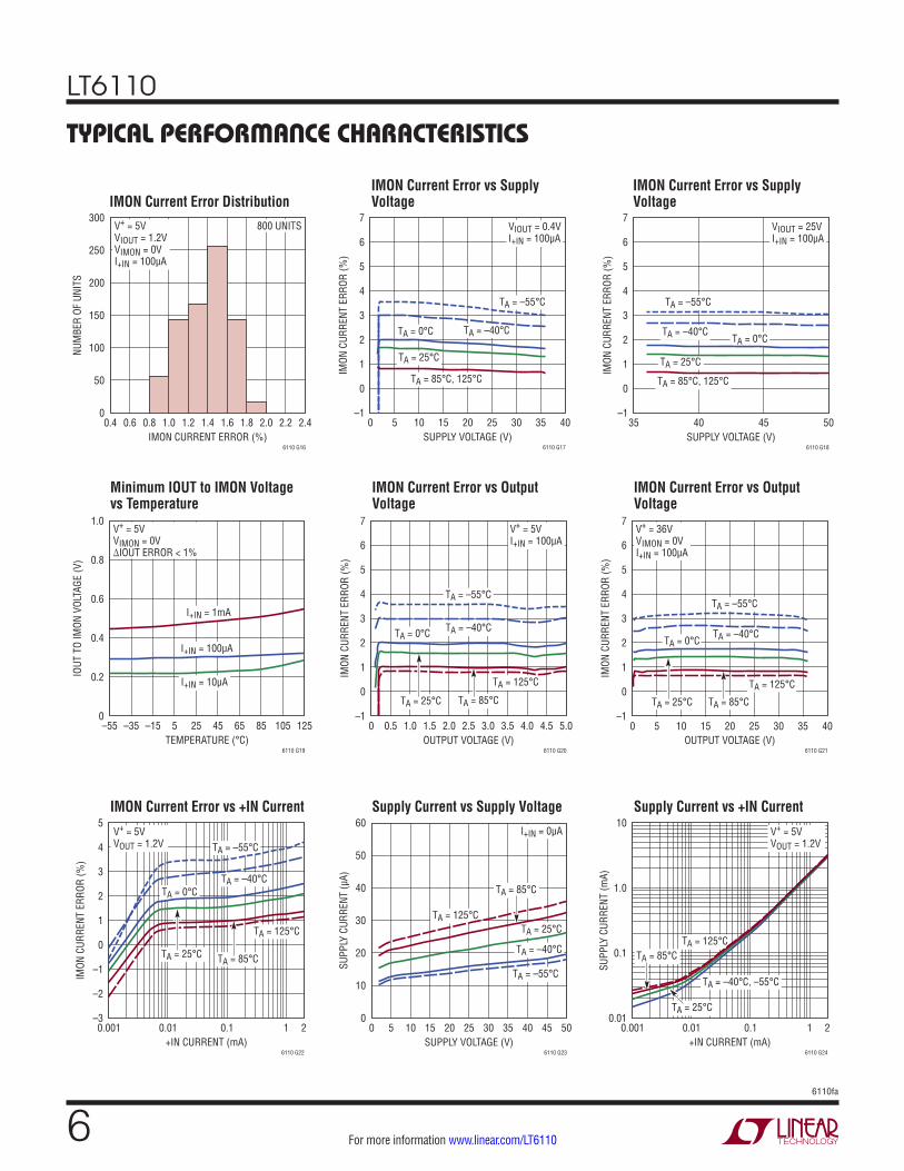
IMON Current Error DistributionIMON Current Error vs Supply Voltage
IMON Current Error vs Supply Voltage
SUPPLY VOLTAGE (V)0
IMON
CUR
RENT
ERR
OR (%
)
7
6
5
3
4
2
–1
0
1
10 205 15 30
6110 G17
4025 35
VIOUT = 0.4VI+IN = 100µA
TA = –55°C
TA = –40°C
TA = 25°C
TA = 0°C
TA = 85°C, 125°C
SUPPLY VOLTAGE (V)
IMON
CUR
RENT
ERR
OR (%
)
6110 G18
TA = 85°C, 125°C
VIOUT = 25VI+IN = 100µA
TA = –55°C
TA = –40°CTA = 0°C
TA = 25°C
35 40 5045
7
6
5
3
4
2
–1
0
1
IMON CURRENT ERROR (%)0.4
NUM
BER
OF U
NITS
0.8 1.2 2.01.6
6110 G16
2.40.6 1.0 1.4 2.21.8
800 UNITSV+ = 5VVIOUT = 1.2VVIMON = 0VI+IN = 100µA
300
200
100
250
150
50
0
LT6110
76110fa
For more information www.linear.com/LT6110
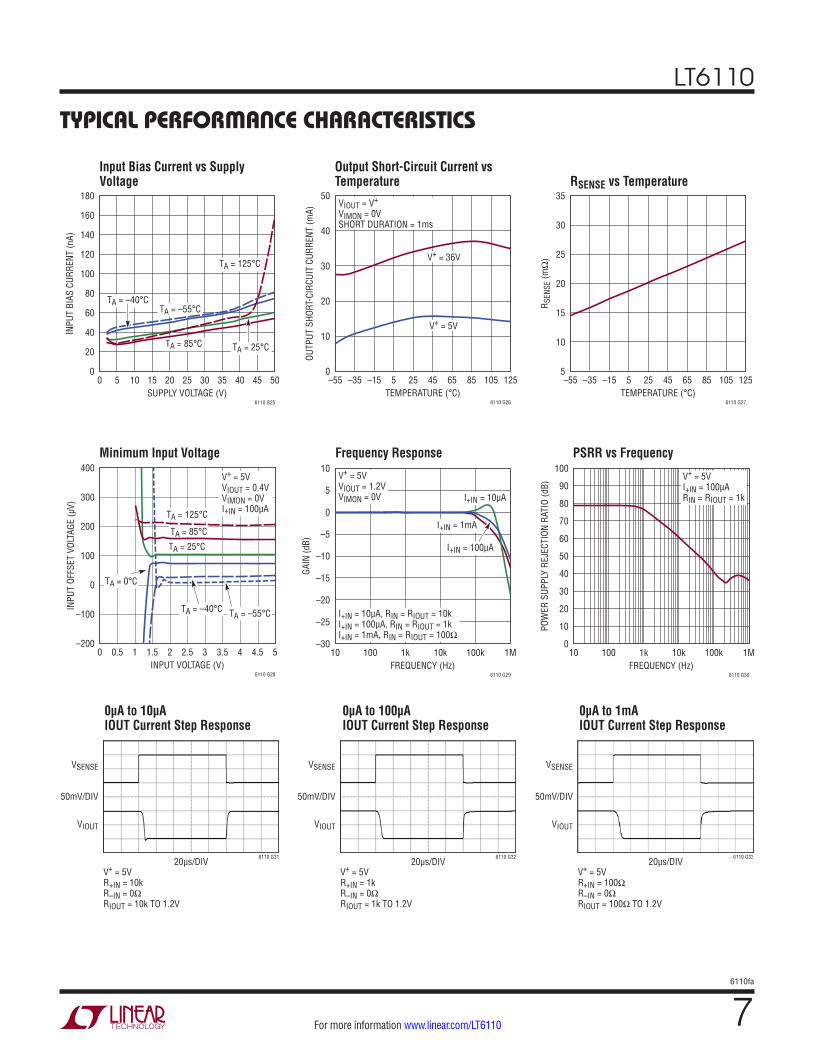
Typical perForMance characTerisTics
0µA to 10µAIOUT Current Step Response
0µA to 100µAIOUT Current Step Response
0µA to 1mAIOUT Current Step Response
Frequency Response PSRR vs Frequency
Input Bias Current vs Supply Voltage
Output Short-Circuit Current vs Temperature RSENSE vs Temperature
SUPPLY VOLTAGE (V)0 5 10 2015 30
6110 G25
5025 454035
INPU
T BI
AS C
URRE
NT (n
A)
180
160
140
120
100
80
60
40
20
0
TA = 25°C
TA = 125°C
TA = –55°CTA = –40°C
TA = 85°C
TEMPERATURE (°C)–55
OUTP
UT S
HORT
-CIR
CUIT
CUR
RENT
(mA)
50
40
20
30
10
0–35 5–15 45
6110 G26
12525 1058565
VIOUT = V+
VIMON = 0VSHORT DURATION = 1ms
V+ = 5V
V+ = 36V
TEMPERATURE (°C)–55
R SEN
SE (m
Ω)
35
20
30
10
25
15
5–35 5–15 45
6110 G27
12525 1058565
FREQUENCY (Hz)10
GAIN
(dB)
10
5
0
–30
–25
–20
–15
–10
–5
100
6110 G29
1M100k10k1k
V+ = 5VVIOUT = 1.2VVIMON = 0V
I+IN = 10µA, RIN = RIOUT = 10kI+IN = 100µA, RIN = RIOUT = 1kI+IN = 1mA, RIN = RIOUT = 100Ω
I+IN = 1mA
I+IN = 10µA
I+IN = 100µA
10 100 100k 1M10k1kFREQUENCY (Hz)
POW
ER S
UPPL
Y RE
JECT
ION
RATI
O (d
B)
6110 G30
100
50
60
70
80
90
40
20
30
10
0
V+ = 5VI+IN = 100µARIN = RIOUT = 1k
20µs/DIV
50mV/DIV
VSENSE
VIOUT
6110 G31
V+ = 5VR+IN = 10kR–IN = 0ΩRIOUT = 10k TO 1.2V
20µs/DIV
50mV/DIV
VSENSE
VIOUT
6110 G32
V+ = 5VR+IN = 1kR–IN = 0ΩRIOUT = 1k TO 1.2V
20µs/DIV
50mV/DIV
VSENSE
VIOUT
6110 G33
V+ = 5VR+IN = 100ΩR–IN = 0ΩRIOUT = 100Ω TO 1.2V
Minimum Input Voltage
INPUT VOLTAGE (V)0
INPU
T OF
FSET
VOL
TAGE
(µV)
400
300
200
–200
–100
0
100
0.5
6110 G28
54.541.51 2.52 3.53
V+ = 5VVIOUT = 0.4VVIMON = 0VI+IN = 100µATA = 125°C
TA = –40°C TA = –55°C
TA = 85°C
TA = 25°C
TA = 0°C

LT6110
86110fa
For more information www.linear.com/LT6110
Typical perForMance characTerisTics
VSENSE = 1V Step Response Unbalanced Inputs
VSENSE = 1V Step Response Balanced Inputs
VSENSE = 5mV Step Response VSENSE = 50mV Step Response VSENSE = 500mV Step Response
100µs/DIV
VSENSE20mV/DIV
VIOUT50mV/DIV
6110 G37
V+ = 5VR+IN = 49.9ΩR–IN = 0ΩRIOUT = 1k TO 1.2V
20µs/DIV
VSENSE500mV/DIV
VIOUT50mV/DIV
6110 G40
V+ = 5VR+IN = 10kR–IN = 0ΩRIOUT = 1k TO 1.2V
20µs/DIV
VSENSE20mV/DIV
VIOUT50mV/DIV
6110 G38
V+ = 5VR+IN = 499ΩR–IN = 0ΩRIOUT = 1k TO 1.2V
20µs/DIV
VSENSE500mV/DIV
VIOUT50mV/DIV
6110 G41
V+ = 5VR+IN = 10kR–IN = 10kRIOUT = 1k TO 1.2V
20µs/DIV
VSENSE200mV/DIV
VIOUT50mV/DIV
6110 G39
V+ = 5VR+IN = 4.99kR–IN = 0ΩRIOUT = 1k TO 1.2V
0µA to 30µAIMON Current Step Response
0µA to 300µAIMON Current Step Response
0µA to 3mAIMON Current Step Response
20µs/DIV
50mV/DIV
VSENSE
VIOUT
6110 G34
V+ = 5VR+IN = 10kR–IN = 0ΩRIMON = 3.4k TO GND
20µs/DIV
50mV/DIV
VSENSE
VIOUT
6110 G35
V+ = 5VR+IN = 1kR–IN = 0ΩRIMON = 340Ω TO GND
20µs/DIV
50mV/DIV
VSENSE
VIOUT
6110 G36
V+ = 5VR+IN = 100ΩR–IN = 0ΩRIMON = 34Ω TO GND
LT6110
96110fa
For more information www.linear.com/LT6110
pin FuncTions (TSOT-23/DFN)
NC (Pin 1/Pin 8): Not Internally Connected.
IOUT (Pin 2/Pin 7): Sinking Current Output. IOUT will sink a current that is equal to VSENSE/RIN. VSENSE is the voltage developed across the sense resisor.
IMON (Pin 3/Pin 6): Sourcing Current Output. IMON will source a current that is equal to 3 • VSENSE/RIN.
V– (Pin 4/Pin 5): Negative Power Supply. Normally con-nected to ground.
–IN (Pin 5/Pin 4): Negative Input to the Internal Sense Amplifier. Must be tied to system load side of the sense resistor, either directly or through a resistor.
RS (Pin 6/Pin 3): Internal Sense Resistor. Connect to the load to use. Leave open when using an external sense resistor.
V+ (Pin 7/Pin 2): Positive Power Supply. Connect to the more positive side of the sense resistor. A minimum ca-pacitance of 0.1µF is required from V+ to V–.
+IN (Pin 8/Pin 1): Positive Input to the Internal Sense Amplifier. The internal sense amplifier will drive +IN to the same potential as –IN. A resistor, R+IN, tied from V+ to +IN sets the IOUT and IMON output currents as defined in the the IOUT and IMON pin functions description.
Exposed Pad (Pin 9, DFN Only): V–. Must be soldered to the PCB.
LT6110
106110fa
For more information www.linear.com/LT6110
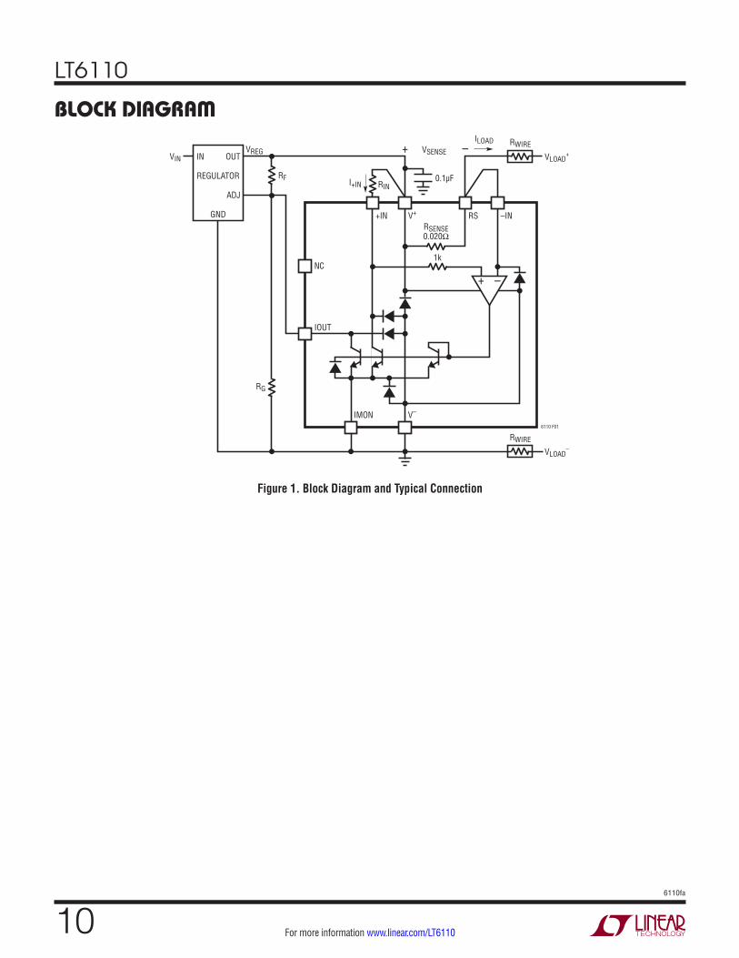
block DiagraM
1k
IOUT
V–
–IN
IMON
NC
+IN
RIN
RG
RF 0.1µFI+IN
VLOAD+
VLOAD–
6110 F01
RSV+
RSENSE0.020Ω
RWIREILOAD
–VSENSE+
RWIRE
+ –
OUTVIN
ADJ
REGULATOR
GND
INVREG
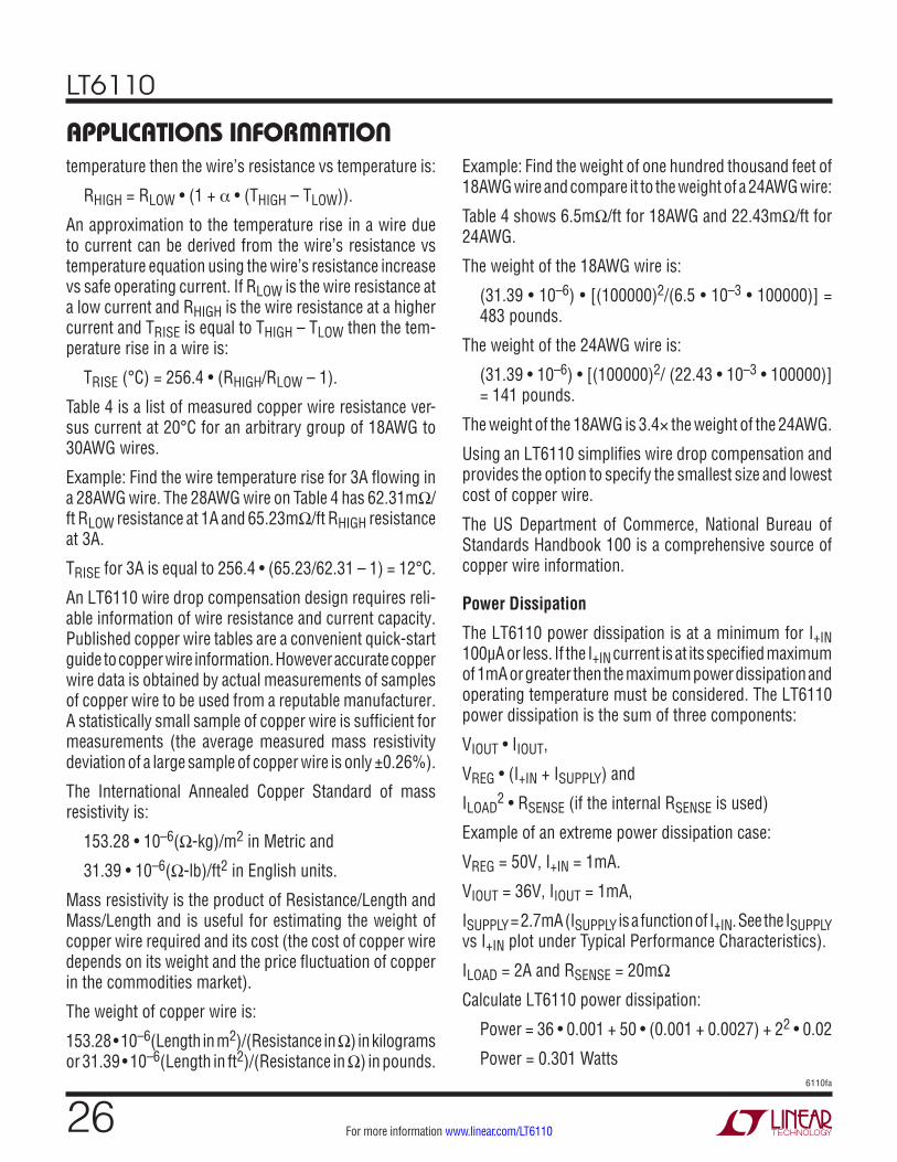
Figure 1. Block Diagram and Typical Connection
LT6110
116110fa
For more information www.linear.com/LT6110
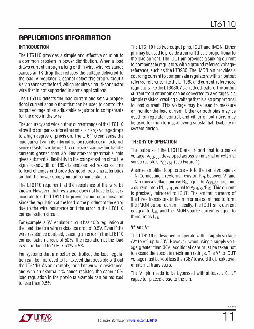
applicaTions inForMaTionINTRODUCTION
The LT6110 provides a simple and effective solution to a common problem in power distribution. When a load draws current through a long or thin wire, wire resistance causes an IR drop that reduces the voltage delivered to the load. A regulator IC cannot detect this drop without a Kelvin sense at the load, which requires a multi-conductor wire that is not supported in some applications.
The LT6110 detects the load current and sets a propor-tional current at an output that can be used to control the output voltage of an adjustable regulator to compensate for the drop in the wire.
The accuracy and wide output current range of the LT6110 allow it to compensate for either small or large voltage drops to a high degree of precision. The LT6110 can sense the load current with its internal sense resistor or an external sense resistor can be used to improve accuracy and handle currents greater than 3A. Resistor-programmable gain gives substantial flexibility to the compensation circuit. A signal bandwidth of 180kHz enables fast response time to load changes and provides good loop characteristics so that the power supply circuit remains stable.
The LT6110 requires that the resistance of the wire be known. However, that resistance does not have to be very accurate for the LT6110 to provide good compensation since the regulation at the load is the product of the error due to the wire resistance and the error in the LT6110 compensation circuit.
For example, a 5V regulator circuit has 10% regulation at the load due to a wire resistance drop of 0.5V. Even if the wire resistance doubled, causing an error in the LT6110 compensation circuit of 50%, the regulation at the load is still reduced to 10% • 50% = 5%.
For systems that are better controlled, the load regula-tion can be improved to far exceed that possible without the LT6110. As an example, for a known wire resistance, and with an external 1% sense resistor, the same 10% load regulation in the previous example can be reduced to less than 0.5%.
The LT6110 has two output pins, IOUT and IMON. Either pin may be used to provide a current that is proportional to the load current. The IOUT pin provides a sinking current to compensate regulators with a ground referred voltage-reference, such as the LT3980. The IMON pin provides a sourcing current to compensate regulators with an output referred reference like the LT1083 and current-referenced regulators like the LT3080. As an added feature, the output current from either pin can be converted to a voltage via a simple resistor, creating a voltage that is also proportional to load current. This voltage may be used to measure or monitor the load current. Either or both pins may be used for regulator control, and either or both pins may be used for monitoring, allowing substantial flexibility in system design.
THEORY OF OPERATION
The outputs of the LT6110 are proportional to a sense voltage, VSENSE, developed across an internal or external sense resistor, RSENSE (see Figure 1).
A sense amplifier loop forces +IN to the same voltage as –IN. Connecting an external resistor, RIN, between V+ and +IN forces a voltage across RIN equal to VSENSE, creating a current into +IN, I+IN , equal to VSENSE/RIN. This current is precisely mirrored to IOUT. The emitter currents of the three transistors in the mirror are combined to form the IMON output current. Ideally, the IOUT sink current is equal to I+IN and the IMON source current is equal to three times I+IN.
V+ and V–
The LT6110 is designed to operate with a supply voltage (V+ to V–) up to 50V. However, when using a supply volt-age greater than 36V, additional care must be taken not to exceed the absolute maximum ratings. The V+ to IOUT voltage must be kept less than 36V to avoid the breakdown of internal transistors.
The V+ pin needs to be bypassed with at least a 0.1µF capacitor placed close to the pin.
LT6110
126110fa
For more information www.linear.com/LT6110
applicaTions inForMaTion+IN and –IN
The +IN and –IN inputs can have a maximum differential voltage equal to the supply voltage. This protects the LT6110 if the –IN pin (the remote load side) is accidentally shorted to ground. In this case, the IOUT current must be limited to less than 2mA (see the Limiting the Regulator Boost Voltage section).
The +IN to IOUT voltage must be kept below 36V to avoid the breakdown of internal transistors.
IOUT and IMON
The IOUT to IMON outputs can have a maximum differ-ential voltage of 36V for IOUT above IMON and –0.6V for IOUT below IMON. A 36V Zener diode can be connected from IOUT to IMON to prevent damage to the output NPN transistor in the event of a fault condition. In this case, a low leakage Zener diode should be used to reduce error in the IOUT current.
RS (Internal RSENSE)
The internal sense resistor can reliably carry a continuous current up to 3A and transient currents of 5A for up to 0.1 seconds. For currents greater than this, an external sense resistor should be used. The internal sense resistor has a temperature coefficient similar to copper.
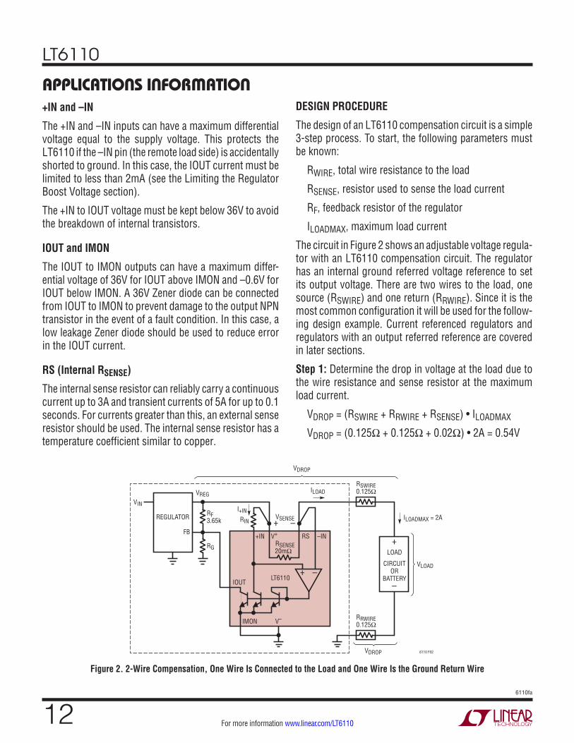
DESIGN PROCEDURE
The design of an LT6110 compensation circuit is a simple 3-step process. To start, the following parameters must be known:
RWIRE, total wire resistance to the load
RSENSE, resistor used to sense the load current
RF, feedback resistor of the regulator
ILOADMAX, maximum load current
The circuit in Figure 2 shows an adjustable voltage regula-tor with an LT6110 compensation circuit. The regulator has an internal ground referred voltage reference to set its output voltage. There are two wires to the load, one source (RSWIRE) and one return (RRWIRE). Since it is the most common configuration it will be used for the follow-ing design example. Current referenced regulators and regulators with an output referred reference are covered in later sections.
Step 1: Determine the drop in voltage at the load due to the wire resistance and sense resistor at the maximum load current.
VDROP = (RSWIRE + RRWIRE + RSENSE) • ILOADMAX
VDROP = (0.125Ω + 0.125Ω + 0.02Ω) • 2A = 0.54V
IOUT
+IN –IN
RIN
I+INILOADMAX = 2A
LT6110
V+
V–
RS
RF3.65k
RG
IMON
+ –
VIN
VREGILOAD
RSWIRE0.125Ω
VDROP
VDROP
RRWIRE0.125Ω
6110 F02
RSENSE20mΩ
VSENSE+ –FB
REGULATOR
VLOAD
LOAD
CIRCUITOR
BATTERY
+
–
Figure 2. 2-Wire Compensation, One Wire Is Connected to the Load and One Wire Is the Ground Return Wire
LT6110
136110fa
For more information www.linear.com/LT6110
applicaTions inForMaTionStep 2: Determine the resistor on the +IN pin, RIN, required to cancel VDROP.
The regulator output voltage will increase as current is pulled from the IOUT pin through the feedback resistor, RF, creating a compensation voltage.
VCOMP = IIOUT • RF
To cancel the voltage drop at the load, set VCOMP equal to VDROP.
VCOMP = IIOUT • RF = VDROP
Since the IOUT current is equal to the current going into the +IN pin and the current in the +IN pin is equal to the sense voltage divided by RIN, RIN can be determined by the following equations:
IIOUT = I+IN =
VSENSERIN
where VSENSE = ILOADMAX • RSENSE
Combining the above equations,
RIN = ILOADMAX • RSENSE( ) • RF
VDROP
RIN = 2A • 0.02Ω( ) • 3.65k
0.54V= 270Ω
Step 3: The final step is to consider the errors in the compensation circuit to determine if the resulting voltage error at the load meets the desired performance.
For example, the internal RSENSE of the LT6110 has a typical tolerance of ±7.5%. If the other errors in the compensation circuit such as VOS, IOUT current error and the resistor tolerances of RF and RIN add an additional ±2.5% error, then the total error in the compensation circuit would be ±10% resulting in a voltage error at the load of the following:
VLOADERROR = VCOMP • Compensation Error
VLOADERROR = 0.54V • (±10%) = ±0.054V
A 10× improvement.
If this is not adequate for the given application, steps can be taken to reduce the sources of error, such as using an
external sense resistor with a tighter tolerance. See the section on External Current Sense Resistors for more information.
In most cases, the internal sense resistor, wire resistance tolerances and temperature mismatch of the RSENSE and RWIRE resistances will contribute the largest portion of the overall compensation circuit error. See the sections on Error Sources, Copper Wire Information and Temperature Errors for a comprehensive discussion.
ADDITIONAL DESIGN CONSIDERATIONS
IOUT Current
The recommended range of IOUT current is 30µA ≤ IIOUT ≤ 300µA for the best precision. For performance outside of this range, see the Typical Performance Curves to determine typical errors.
If the IOUT current is less than 30µA, the feedback resis-tor may need to be adjusted to reduce the error in the compensation circuit.
In the previous example,
IIOUT =
VSENSERIN
= 0.04270
= 148µA
Since this is within the recommended range no further adjustment is needed.
See the section on Compensating a Low Quiescent Current Design for IOUT current less than 30µA.
Load Regulation
Load regulation is often specified as an error in output voltage at a given load current, as in the previous example, but it is also specified as a percentage of the regulator output voltage. If the output voltage of the regulator circuit in Figure 2 is 5V, the resulting compensated load regula-tion, in percent, would be the following:
LoadRegCOMP %( ) =VLOADERROR
VREG• 100
LoadRegCOMP %( ) =±0.054V
5V• 100 = ±1.1%
LT6110
146110fa
For more information www.linear.com/LT6110
applicaTions inForMaTionWithout the compensation circuit (no RSENSE) the load regulation in percent would be,
LoadRegUNCOMP %( ) =
–0.5V5V
• 100 = –10%
The regulator’s output will also change due to its own load regulation effects (per the regulator’s specification). In general, this change in voltage is small compared to the wire-drop, and can be ignored. If it is considered to be a significant source of error, it can be included as part of the wire-drop compensation. To include the regulator’s load regulation effect, simply add the voltage drop due to the regulator’s load regulation at ILOADMAX to VDROP, when calculating the compensation circuit parameters.
PCB Trace Resistance
Printed circuit trace resistance between the output of the regulator and the load will cause additional voltage drops. As with the regulator’s load regulation effects, these drops can be compensated for by adding them to VDROP when calculating the compensation circuit parameters. This also allows the use of narrower traces to deliver power to the load and still retain good load regulation. See the PCB Copper Resistor section for more information on how to determine trace resistance.
Kelvin Sense Connection to RSENSE
To reduce RSENSE error due to trace resistance, the –IN pin and RIN resistor should be connected as close to RSENSE as possible, as reflected in Figure 2.
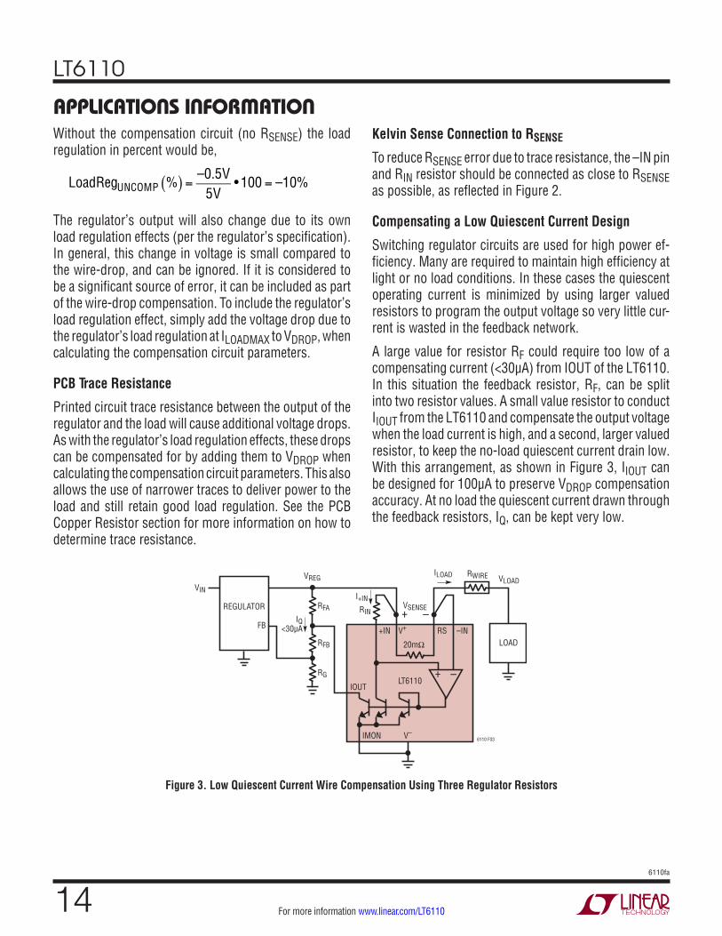
Compensating a Low Quiescent Current Design
Switching regulator circuits are used for high power ef-ficiency. Many are required to maintain high efficiency at light or no load conditions. In these cases the quiescent operating current is minimized by using larger valued resistors to program the output voltage so very little cur-rent is wasted in the feedback network.
A large value for resistor RF could require too low of a compensating current (<30µA) from IOUT of the LT6110. In this situation the feedback resistor, RF, can be split into two resistor values. A small value resistor to conduct IIOUT from the LT6110 and compensate the output voltage when the load current is high, and a second, larger valued resistor, to keep the no-load quiescent current drain low. With this arrangement, as shown in Figure 3, IIOUT can be designed for 100µA to preserve VDROP compensation accuracy. At no load the quiescent current drawn through the feedback resistors, IQ, can be kept very low.
IOUT
+IN –IN
RIN
LT6110
V+
V–
RS
RFA
RFB
RG
IMON
+ –
VIN
VREGILOAD RWIRE VLOAD
6110 F03
20mΩ
+ –FB
IQ<30µA
REGULATOR
LOAD
I+IN VSENSE
Figure 3. Low Quiescent Current Wire Compensation Using Three Regulator Resistors
LT6110
156110fa
For more information www.linear.com/LT6110
applicaTions inForMaTionIn Figure 3 RF is split into RFA and RFB. VREG is the no-load quiescent output voltage of the regulator. The design of these two feedback resistors follows:
RFA =
VDROPIIOUT
IIOUT can be sized to be 100µA at full load current and only this resistor creates the VDROP compensation voltage.
RFB =
VREG – VFBIQ
– RFA
IQ is the no-load quiescent current flowing through the resistor string.
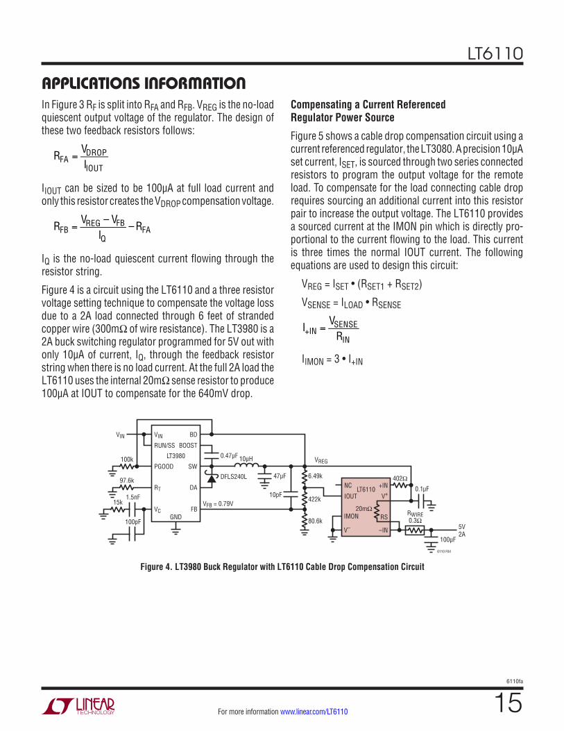
Figure 4 is a circuit using the LT6110 and a three resistor voltage setting technique to compensate the voltage loss due to a 2A load connected through 6 feet of stranded copper wire (300mΩ of wire resistance). The LT3980 is a 2A buck switching regulator programmed for 5V out with only 10µA of current, IQ, through the feedback resistor string when there is no load current. At the full 2A load the LT6110 uses the internal 20mΩ sense resistor to produce 100µA at IOUT to compensate for the 640mV drop.
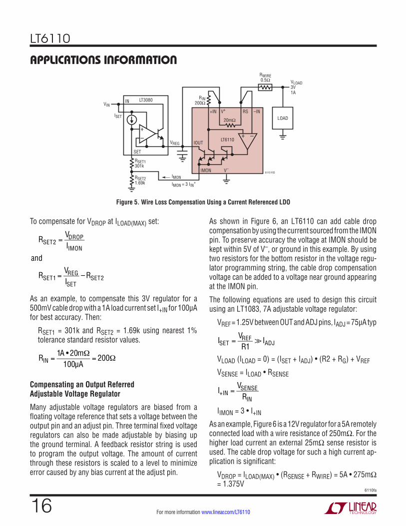
Compensating a Current Referenced Regulator Power Source
Figure 5 shows a cable drop compensation circuit using a current referenced regulator, the LT3080. A precision 10µA set current, ISET, is sourced through two series connected resistors to program the output voltage for the remote load. To compensate for the load connecting cable drop requires sourcing an additional current into this resistor pair to increase the output voltage. The LT6110 provides a sourced current at the IMON pin which is directly pro-portional to the current flowing to the load. This current is three times the normal IOUT current. The following equations are used to design this circuit:
VREG = ISET • (RSET1 + RSET2)
VSENSE = ILOAD • RSENSE
I+IN =
VSENSERIN
IIMON = 3 • I+IN
Figure 4. LT3980 Buck Regulator with LT6110 Cable Drop Compensation Circuit
15k1.5nF
0.1µF
100pF
VINVIN BD
RUN/SS
0.47µF
47µF
10pF
VREG
6.49k
422k
10µH
DFLS240L
LT3980
GND
100k
80.6k
VFB = 0.79V
97.6k
BOOST
NC +IN
IOUTLT6110
V+
RSIMON
–INV–
20mΩ
PGOOD SW
RT DA
VC FB
100µF
6110 F04
5V2A
RWIRE0.3Ω
402Ω
LT6110
166110fa
For more information www.linear.com/LT6110
applicaTions inForMaTion
To compensate for VDROP at ILOAD(MAX) set:
RSET2 =VDROPIIMON
and
RSET1 =VREGISET
– RSET2
As an example, to compensate this 3V regulator for a 500mV cable drop with a 1A load current set I+IN for 100µA for best accuracy. Then:
RSET1 = 301k and RSET2 = 1.69k using nearest 1% tolerance standard resistor values.
RIN =
1A • 20mΩ100µA
= 200Ω
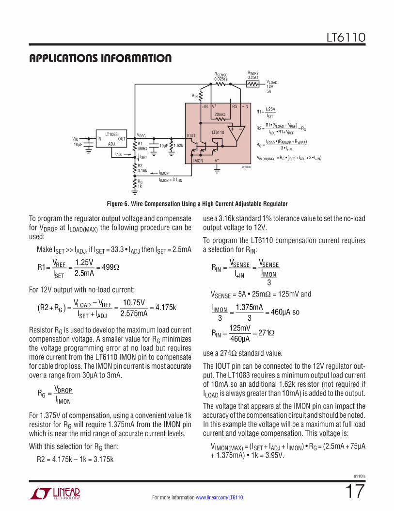
Compensating an Output Referred Adjustable Voltage Regulator
Many adjustable voltage regulators are biased from a floating voltage reference that sets a voltage between the output pin and an adjust pin. Three terminal fixed voltage regulators can also be made adjustable by biasing up the ground terminal. A feedback resistor string is used to program the output voltage. The amount of current through these resistors is scaled to a level to minimize error caused by any bias current at the adjust pin.
As shown in Figure 6, an LT6110 can add cable drop compensation by using the current sourced from the IMON pin. To preserve accuracy the voltage at IMON should be kept within 5V of V–, or ground in this example. By using two resistors for the bottom resistor in the voltage regu-lator programming string, the cable drop compensation voltage can be added to a voltage near ground appearing at the IMON pin.
The following equations are used to design this circuit using an LT1083, 7A adjustable voltage regulator:
VREF = 1.25V between OUT and ADJ pins, IADJ = 75µA typ
ISET =
VREFR1
IADJ
VLOAD (ILOAD = 0) = (ISET + IADJ) • (R2 + RG) + VREF
VSENSE = ILOAD • RSENSE
I+IN =
VSENSERIN
IIMON = 3 • I+IN
As an example, Figure 6 is a 12V regulator for a 5A remotely connected load with a wire resistance of 250mΩ. For the higher load current an external 25mΩ sense resistor is used. The cable drop voltage for such a high current ap-plication is significant:
VDROP = ILOAD(MAX) • (RSENSE + RWIRE) = 5A • 275mΩ = 1.375V
Figure 5. Wire Loss Compensation Using a Current Referenced LDO
IOUT
+IN –IN
RIN200Ω
LT6110
V+
V–
RS
IMONIMON
IMON = 3 IIN+
+ –
VIN
RWIRE0.5Ω VLOAD
3V1A
6110 F05
20mΩ
IN LT3080
ISET
SET
RSET1301k
RSET21.69k
VREG
LOAD
+–
LT6110
176110fa
For more information www.linear.com/LT6110
applicaTions inForMaTion
To program the regulator output voltage and compensate for VDROP at ILOAD(MAX) the following procedure can be used:
Make ISET >> IADJ, if ISET = 33.3 • IADJ then ISET = 2.5mA
R1=
VREFISET
=1.25V2.5mA
= 499Ω
For 12V output with no-load current:
R2+RG( ) =
VLOAD – VREFISET +IADJ
=10.75V
2.575mA= 4.175k
Resistor RG is used to develop the maximum load current compensation voltage. A smaller value for RG minimizes the voltage programming error at no load but requires more current from the LT6110 IMON pin to compensate for cable drop loss. The IMON pin current is most accurate over a range from 30µA to 3mA.
RG =
VDROPIIMON
For 1.375V of compensation, using a convenient value 1k resistor for RG will require 1.375mA from the IMON pin which is near the mid range of accurate current levels.
With this selection for RG then:
R2 = 4.175k – 1k = 3.175k
use a 3.16k standard 1% tolerance value to set the no-load output voltage to 12V.
To program the LT6110 compensation current requires a selection for RIN:
RIN =VSENSE
I+IN=
VSENSEIIMON
3 VSENSE = 5A • 25mΩ = 125mV and
IIMON3
=1.375mA
3= 460µA so
RIN =125mV460µA
= 271Ω
use a 274Ω standard value.
The IOUT pin can be connected to the 12V regulator out-put. The LT1083 requires a minimum output load current of 10mA so an additional 1.62k resistor (not required if ILOAD is always greater than 10mA) is added to the output.
The voltage that appears at the IMON pin can impact the accuracy of the compensation circuit and should be noted. In this example the voltage will be a maximum at full load current and voltage compensation. This voltage is:
VIMON(MAX) = (ISET + IADJ + IIMON) • RG = (2.5mA + 75µA + 1.375mA) • 1k = 3.95V.
IOUT
+IN –IN
RIN
LT6110
V+
V–
RS
IMON
IIMON
IIMON = 3 I+IN
+ –
RWIRE0.25Ω
VLOAD12V5A
6110 F06
20mΩ
R23.16k
R1499Ω
RG1k
VREGVIN
IADJ
10µF 1.62k
RSENSE0.025Ω
ISET
10µFOUTIN
LT1083
ADJ
R1= 1.25VISET
R2=R1• VLOAD – VREF( )
IADJ •R1+ VREF– RG
RG =ILOAD • RSENSE +RWIRE( )
3 • I+IN
VIMON(MAX) =RG • ISET +IADJ +3 • I+IN( )
Figure 6. Wire Compensation Using a High Current Adjustable Regulator
LT6110
186110fa
For more information www.linear.com/LT6110
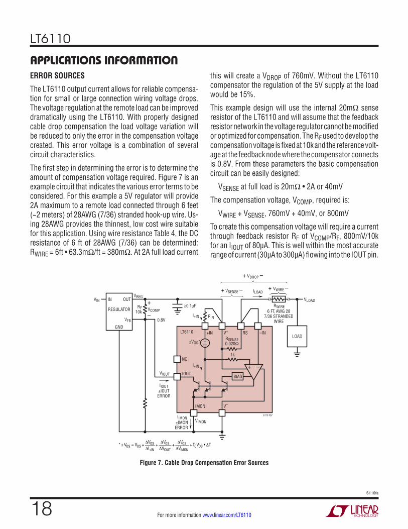
applicaTions inForMaTionERROR SOURCES
The LT6110 output current allows for reliable compensa-tion for small or large connection wiring voltage drops. The voltage regulation at the remote load can be improved dramatically using the LT6110. With properly designed cable drop compensation the load voltage variation will be reduced to only the error in the compensation voltage created. This error voltage is a combination of several circuit characteristics.
The first step in determining the error is to determine the amount of compensation voltage required. Figure 7 is an example circuit that indicates the various error terms to be considered. For this example a 5V regulator will provide 2A maximum to a remote load connected through 6 feet (~2 meters) of 28AWG (7/36) stranded hook-up wire. Us-ing 28AWG provides the thinnest, low cost wire suitable for this application. Using wire resistance Table 4, the DC resistance of 6 ft of 28AWG (7/36) can be determined: RWIRE = 6ft • 63.3mΩ/ft = 380mΩ. At 2A full load current
this will create a VDROP of 760mV. Without the LT6110 compensator the regulation of the 5V supply at the load would be 15%.
This example design will use the internal 20mΩ sense resistor of the LT6110 and will assume that the feedback resistor network in the voltage regulator cannot be modified or optimized for compensation. The RF used to develop the compensation voltage is fixed at 10k and the reference volt-age at the feedback node where the compensator connects is 0.8V. From these parameters the basic compensation circuit can be easily designed:
VSENSE at full load is 20mΩ • 2A or 40mV
The compensation voltage, VCOMP, required is:
VWIRE + VSENSE, 760mV + 40mV, or 800mV
To create this compensation voltage will require a current through feedback resistor RF of VCOMP/RF, 800mV/10k for an IIOUT of 80µA. This is well within the most accurate range of current (30µA to 300µA) flowing into the IOUT pin.
1k
IOUTVIOUT
V–
–IN
IMON
VIMON
NC
LT6110 +IN
±VOS*
RIN
VCOMP≥0.1µF
0.8VI+IN
I+IN
VLOAD
6 FT, AWG 287/36 STRANDED
WIRE
6110 F07
RSV+
RSENSE0.020Ω
RWIRE
+ VWIRE –ILOAD
IIOUT±IOUTERROR
±IMONERROR
+ VSENSE –
+ VDROP –
+ –
OUT
RF10k
VIN
VFB
REGULATOR
GND
INVREG
LOAD
BIAS
+–
+
–
IIMON
*± VOS = VOS +
ΔVOSΔI+IN
+ΔVOSΔVIOUT
+ΔVOSΔVIMON
+TCVOS •ΔT
Figure 7. Cable Drop Compensation Error Sources

LT6110
196110fa
For more information www.linear.com/LT6110
applicaTions inForMaTionTo create this current at full load requires an RIN value of VSENSE/IIOUT, 40mV/80µA, or 500Ω. Using the nearest standard 1% tolerance value of 499Ω will be sufficient. Without considering any error terms other than this slight change in value for RIN results in nearly perfect cable drop compensation. The theoretical load regulation would be improved from 15% to less than 0.01%.
The single largest source of compensation error comes from any change in the connecting wire resistance from the design assumptions. This could be caused by temperature, aging and possibly corrosion. In the compensator circuit, component tolerances and errors terms will combine to deviate from the near perfect designed amount of com-pensation. Figure 7 shows this simple example design and indicates the various error sources within the LT6110. All of the error terms can be determined from the Electrical Characteristics Table. The error terms for any compensa-tor design include:
• RSENSE tolerance• RIN tolerance• RF tolerance• VOS, the offset voltage in µV of the internal current
sense amplifier• ∆VOS/∆I+IN is an error term caused by the finite gain
of the current sense amplifier.
This is the change in the offset voltage as the sense voltage and resulting input current varies from 0 to the maximum value. It is a factor specified in mV/mA which is ohms and is accounted for as a small resistance in series with RIN. The voltage across this small resistance is included in the total offset voltage term. The change in I+IN current is relative to 100µA where the LT6110 is trimmed for accuracy.
• ∆VOS/∆VIOUT is a change in the offset voltage caused by a change in the voltage applied to the IOUT pin specified in mV/V. The change in VIOUT is relative to 1.2V DC where the LT6110 is trimmed for accuracy.
• ∆VOS/∆VIMON is a change in the offset voltage caused by a change in the voltage applied to the IMON pin specified in mV/V.
• IOUT current error is the accuracy of the internal current mirror. This is a percent deviation from I+IN.
• IMON current error is the accuracy of the total internal mirror current sourced to the IMON output. This is a percent deviation from 3 • I+IN.
• Temperature Related Errors (see Temperature Errors section)
Table 1 is an example of the stack-up of all error terms in the design of Figure 7. This table uses typical variances to be seen at 25°C. It is not a rigorous worst case analysis over all possible operating conditions, but instead serves to illustrate what to expect for load regulation improvement under nominal conditions.
In this example, including all typical error terms, the LT6110 still provides a factor of 10 improvement in voltage regula-tion at the remote load. To obtain the same level of load voltage stability without using the LT6110 would require reducing the amount of cable drop loss. The easiest way to do so would be to increase the wire gauge used to connect to the load. For a 76mV change in load voltage at 2A full load current would require a wire resistance of only 38mΩ and a 6 foot length 18AWG gauge wire is required. A larger wire gauge can be significantly more costly and is less flexible in routing to the load. These are two significant design compromises to be considered.
LT6110
206110fa
For more information www.linear.com/LT6110
applicaTions inForMaTion
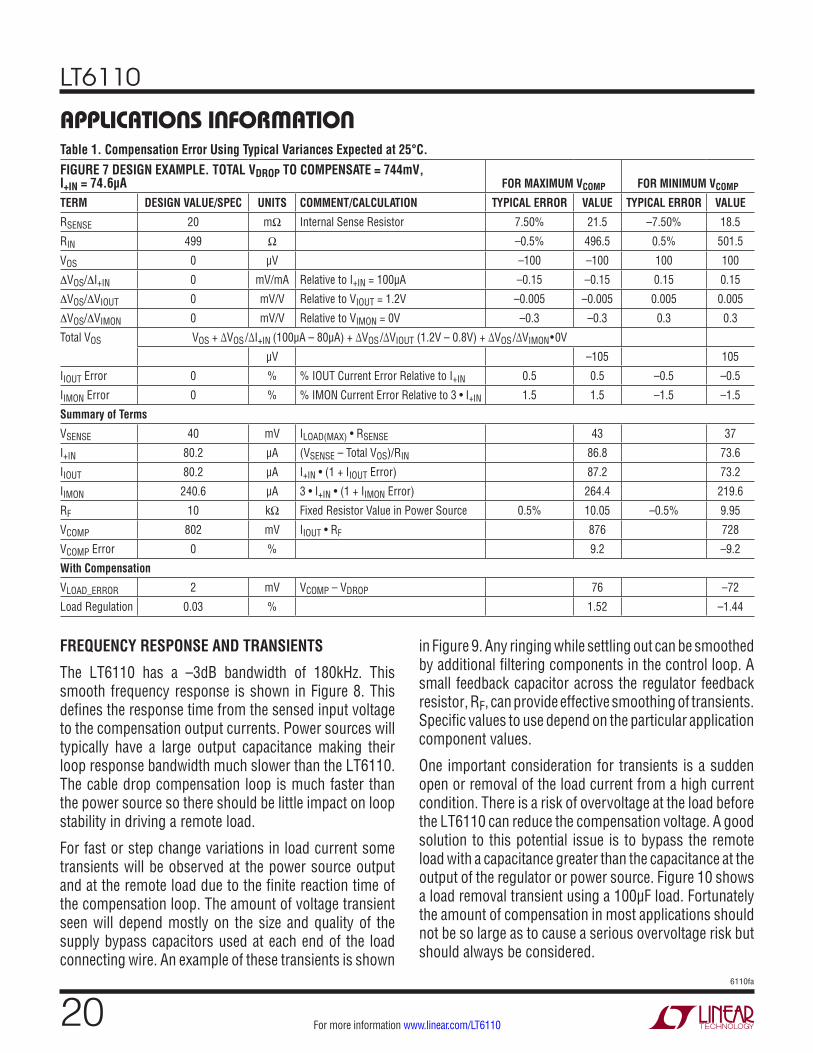
FREQUENCY RESPONSE AND TRANSIENTS
The LT6110 has a –3dB bandwidth of 180kHz. This smooth frequency response is shown in Figure 8. This defines the response time from the sensed input voltage to the compensation output currents. Power sources will typically have a large output capacitance making their loop response bandwidth much slower than the LT6110. The cable drop compensation loop is much faster than the power source so there should be little impact on loop stability in driving a remote load.
For fast or step change variations in load current some transients will be observed at the power source output and at the remote load due to the finite reaction time of the compensation loop. The amount of voltage transient seen will depend mostly on the size and quality of the supply bypass capacitors used at each end of the load connecting wire. An example of these transients is shown
in Figure 9. Any ringing while settling out can be smoothed by additional filtering components in the control loop. A small feedback capacitor across the regulator feedback resistor, RF, can provide effective smoothing of transients. Specific values to use depend on the particular application component values.
One important consideration for transients is a sudden open or removal of the load current from a high current condition. There is a risk of overvoltage at the load before the LT6110 can reduce the compensation voltage. A good solution to this potential issue is to bypass the remote load with a capacitance greater than the capacitance at the output of the regulator or power source. Figure 10 shows a load removal transient using a 100µF load. Fortunately the amount of compensation in most applications should not be so large as to cause a serious overvoltage risk but should always be considered.
Table 1. Compensation Error Using Typical Variances Expected at 25°C. FIGURE 7 DESIGN EXAMPLE. TOTAL VDROP TO COMPENSATE = 744mV, I+IN = 74.6µA FOR MAXIMUM VCOMP FOR MINIMUM VCOMP
TERM DESIGN VALUE/SPEC UNITS COMMENT/CALCULATION TYPICAL ERROR VALUE TYPICAL ERROR VALUE
RSENSE 20 mΩ Internal Sense Resistor 7.50% 21.5 –7.50% 18.5
RIN 499 Ω –0.5% 496.5 0.5% 501.5
VOS 0 µV –100 –100 100 100
∆VOS/∆I+IN 0 mV/mA Relative to I+IN = 100µA –0.15 –0.15 0.15 0.15
∆VOS/∆VIOUT 0 mV/V Relative to VIOUT = 1.2V –0.005 –0.005 0.005 0.005
∆VOS/∆VIMON 0 mV/V Relative to VIMON = 0V –0.3 –0.3 0.3 0.3
Total VOS VOS + ∆VOS/∆I+IN (100µA – 80µA) + ∆VOS/∆VIOUT (1.2V – 0.8V) + ∆VOS/∆VIMON•0V
µV –105 105
IIOUT Error 0 % % IOUT Current Error Relative to I+IN 0.5 0.5 –0.5 –0.5
IIMON Error 0 % % IMON Current Error Relative to 3 • I+IN 1.5 1.5 –1.5 –1.5
Summary of Terms
VSENSE 40 mV ILOAD(MAX) • RSENSE 43 37
I+IN 80.2 µA (VSENSE – Total VOS)/RIN 86.8 73.6
IIOUT 80.2 µA I+IN • (1 + IIOUT Error) 87.2 73.2
IIMON 240.6 µA 3 • I+IN • (1 + IIMON Error) 264.4 219.6
RF 10 kΩ Fixed Resistor Value in Power Source 0.5% 10.05 –0.5% 9.95
VCOMP 802 mV IIOUT • RF 876 728
VCOMP Error 0 % 9.2 –9.2
With Compensation
VLOAD_ERROR 2 mV VCOMP – VDROP 76 –72
Load Regulation 0.03 % 1.52 –1.44
LT6110
216110fa
For more information www.linear.com/LT6110
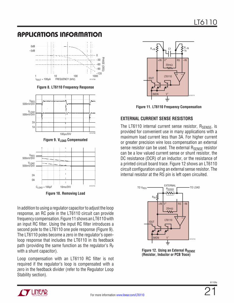
applicaTions inForMaTion
In addition to using a regulator capacitor to adjust the loop response, an RC pole in the LT6110 circuit can provide frequency compensation. Figure 11 shows an LT6110 with an input RC filter. Using the input RC filter introduces a second pole to the LT6110 one pole response (Figure 9). The LT6110 poles become a zero in the regulator’s open-loop response that includes the LT6110 in its feedback path (providing the same function as the regulator’s RF with a shunt capacitor).
Loop compensation with an LT6110 RC filter is not required if the regulator’s loop is compensated with a zero in the feedback divider (refer to the Regulator Loop Stability section).
0dB
–3dB
0
–30
–60
PHASE (DEG)–90
–1201 10
FREQUENCY (kHz)IIOUT = 100µA100 1000
6110 F08
Figure 8. LT6110 Frequency Response
Figure 11. LT6110 Frequency Compensation
Figure 12. Using an External RSENSE (Resistor, Inductor or PCB Trace)
Figure 9. VLOAD Compensated
Figure 10. Removing Load
VREG500mV/DIV
VLOAD500mV/DIV
2A
1A
100µs/DIV 6110 F09
VREG500mV/DIV
VLOAD500mV/DIV
2A
0A
CLOAD = 100µF 10ms/DIV 6110 F10
EXTERNAL CURRENT SENSE RESISTORS
The LT6110 internal current sense resistor, RSENSE, is provided for convenient use in many applications with a maximum load current less than 3A. For higher current or greater precision wire loss compensation an external sense resistor can be used. The external RSENSE resistor can be a low valued current sense or shunt resistor, the DC resistance (DCR) of an inductor, or the resistance of a printed circuit board trace. Figure 12 shows an LT6110 circuit configuration using an external sense resistor. The internal resistor at the RS pin is left open circuited.
IOUT
+IN –IN
R–IN1k
R+IN
LT6110
V+
V–
RS
IMON
+ –
6110 F11
20mΩ
C1
IOUT
+IN –IN
RIN
TO VREG TO LOAD
LT6110
V+
V–
RS
IMON
+ –
6110 F12
20mΩ
EXTERNALRSENSE
LT6110
226110fa
For more information www.linear.com/LT6110
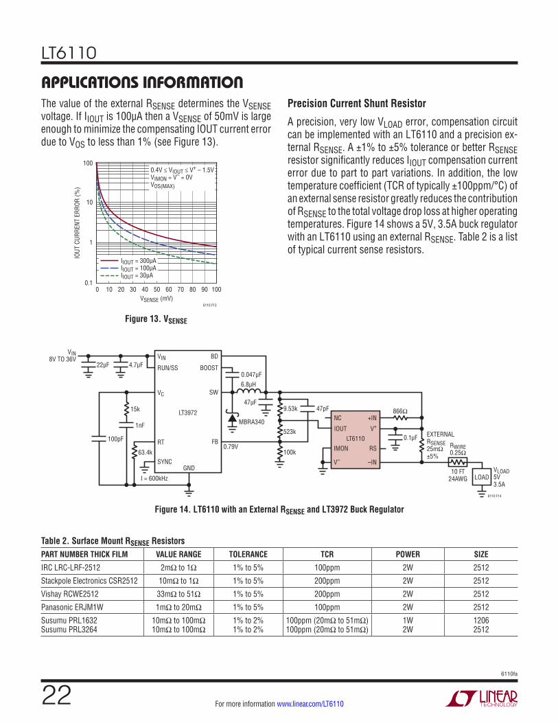
applicaTions inForMaTionThe value of the external RSENSE determines the VSENSE voltage. If IIOUT is 100µA then a VSENSE of 50mV is large enough to minimize the compensating IOUT current error due to VOS to less than 1% (see Figure 13).
Figure 13. VSENSE
Figure 14. LT6110 with an External RSENSE and LT3972 Buck Regulator
Precision Current Shunt Resistor
A precision, very low VLOAD error, compensation circuit can be implemented with an LT6110 and a precision ex-ternal RSENSE. A ±1% to ±5% tolerance or better RSENSE resistor significantly reduces IIOUT compensation current error due to part to part variations. In addition, the low temperature coefficient (TCR of typically ±100ppm/°C) of an external sense resistor greatly reduces the contribution of RSENSE to the total voltage drop loss at higher operating temperatures. Figure 14 shows a 5V, 3.5A buck regulator with an LT6110 using an external RSENSE. Table 2 is a list of typical current sense resistors.
VSENSE (mV)0 10 20 30
IOUT
CUR
RENT
ERR
OR (%
)
1
10
100
40 50 60 70 80 90 100
6110 F13
0.1
IIOUT = 300µAIIOUT = 100µAIIOUT = 30µA
0.4V ≤ VIOUT ≤ V+ – 1.5VVIMON = V– = 0VVOS(MAX)
63.4k
I = 600kHz
VINVIN
8V TO 36VRUN/SS
0.047µF
47µF
MBRA340
0.79V
47pF9.53k
523k
6.8µH
LT3972
GND
100k
BD
NC +IN
IOUTLT6110
V+
RSIMON
–INV–
BOOST
SW
RT
15k
VC
SYNC
FB
6110 F14
VLOAD5V3.5A
0.1µF
22µF 4.7µF
RWIRE0.25Ω
10 FT24AWG
EXTERNALRSENSE25mΩ±5%
866Ω
LOAD
1nF
100pF
Table 2. Surface Mount RSENSE ResistorsPART NUMBER THICK FILM VALUE RANGE TOLERANCE TCR POWER SIZE
IRC LRC-LRF-2512 2mΩ to 1Ω 1% to 5% 100ppm 2W 2512
Stackpole Electronics CSR2512 10mΩ to 1Ω 1% to 5% 200ppm 2W 2512
Vishay RCWE2512 33mΩ to 51Ω 1% to 5% 200ppm 2W 2512
Panasonic ERJM1W 1mΩ to 20mΩ 1% to 5% 100ppm 2W 2512
Susumu PRL1632 Susumu PRL3264
10mΩ to 100mΩ 10mΩ to 100mΩ
1% to 2% 1% to 2%
100ppm (20mΩ to 51mΩ) 100ppm (20mΩ to 51mΩ)
1W 2W
1206 2512

LT6110
236110fa
For more information www.linear.com/LT6110
applicaTions inForMaTionCopper Resistor Made from an RF Inductor
An inductor made of copper wire will have a small DC resistance, DCR or RCOIL, with a temperature coefficient that matches that of the copper wire connecting the remote load. Copper wire resistance has a positive temperature coefficient of approximately +3900ppm/°C. If the current sense resistor and the remote load are in the same operat-ing environment and subject to an increase in temperature, the resistance increase in RSENSE will increase both VSENSE and the LT6110 compensation current to directly track and cancel the increase in wire voltage drop to the load(refer to the Temperature Errors section). Table 3 shows a list of small air core inductors suitable for use as external RSENSE resistors.
Table 3. Coilcraft Air Core Inductors for External RSENSE
COILCRAFT PART NUMBER
INDUCTANCE (nH)*
DCR NOMINAL (mΩ) (±6% TYPICAL)
IRMS (A)
0908SQ-27N 27 8.5 4.4
2222SQ-221 221 9.8 5
1010 US-141 146 3.1 14
*Inductance is not relevant for current sense.
PCB Copper Resistor
In a high load current application without a high preci-sion load regulation specification, the cost of an external RSENSE resistor can be eliminated using the resistance of a printed circuit board, PCB, trace as a sense resistor. The resistance, RPCB, is a function of copper resistivity (ρ), PCB copper thickness (T), trace width (W) and trace length (L), RPCB = ρ (L/(T • W)). The typical manufacturing of PCB fabrication limits the trace resistance tolerance to ±15%. A simplified RPCB calculation sets the length equal to the width (L/W = 1) and approximates 0.5mΩ and 0.25mΩ per square trace area for 1oz and 2oz copper respectively. The maximum current of a PCB trace depends on the trace cross sectional area, trace width (W) times cop-per thickness (T) and the amount of heating of the trace permitted. Figure 15 plots PCB trace current vs PCB trace width for 1oz (T = 1.4mils) and 2oz (T = 2.8mils) copper for less than 10˚C temperature rise (this graph provides a conservative maximum trace current estimate based on the ANSI IPC2221 standard).
Example: Design a 2oz copper PCB trace sense resistor to compensate for wire voltage drop for an ILOAD(MAX) of 10A.
A VSENSE of 60mV is large enough to minimize the com-pensating IOUT current error due to the input offset voltage of the LT6110.
RPCB =
VSENSEILOAD(MAX)
=60mV10A
= 6mΩ
Using Figure 15, the 2oz copper minimum trace width for 10A is 150mils. This sets the current handling capability of the trace.
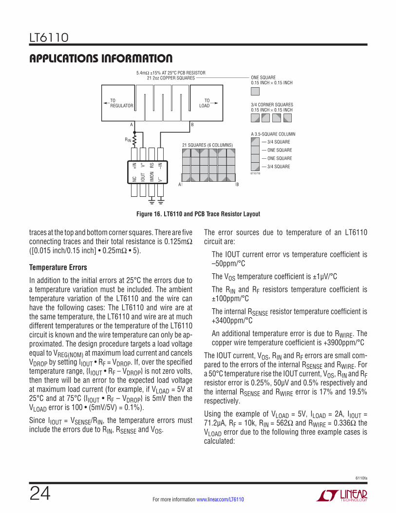
The resistance of the trace resistor is set by the length of the trace. Each 150mil wide square of 2oz copper will have a resistance of 0.25mΩ. A total resistance of 6mΩ will require 24 squares (6mΩ/0.25mΩ/square). The length of the PCB trace will then be 24sq × 150mils or 3.6 inches.
A serpentine layout can be used to reduce the footprint of RPCB. Figure 16 shows a serpentine layout for a 6mΩ PCB sense resistor and the VSENSE connections to the LT6110. The corners of the serpentine resistor count as 3/4 of a square. In Figure 16, RPCB consists of six 3.5 square rect-angular traces (two whole squares and two 3/4 squares). The RPCB six rectangular traces equal 21 0.15in × 0.15in squares. Using a 2oz copper trace the resistance of the 21 squares is 5.25mΩ at 25°C (21 • 0.25mΩ per square). An additional very small trace resistance is due to the 0.015in × 0.15in trace that connects the rectangular
PCB TRACE WIDTH (MILS)0
PCB
TRAC
E CU
RREN
T (A
)
12
16
20
24
400 450
6110 F15
8
4
10
14
18
22
6
2
050 100 150 200 250 300 350 500
2oz COPPER
1oz COPPER
Figure 15. PCB Trace Current vs Trace Width (<10°C Temperature Rise)
LT6110
246110fa
For more information www.linear.com/LT6110
applicaTions inForMaTion
traces at the top and bottom corner squares. There are five connecting traces and their total resistance is 0.125mΩ ([0.015 inch/0.15 inch] • 0.25mΩ • 5).
Temperature Errors
In addition to the initial errors at 25°C the errors due to a temperature variation must be included. The ambient temperature variation of the LT6110 and the wire can have the following cases: The LT6110 and wire are at the same temperature, the LT6110 and wire are at much different temperatures or the temperature of the LT6110 circuit is known and the wire temperature can only be ap-proximated. The design procedure targets a load voltage equal to VREG(NOM) at maximum load current and cancels VDROP by setting IIOUT • RF = VDROP. If, over the specified temperature range, IIOUT • RF – VDROP is not zero volts, then there will be an error to the expected load voltage at maximum load current (for example, if VLOAD = 5V at 25°C and at 75°C IIOUT • RF – VDROP is 5mV then the VLOAD error is 100 • (5mV/5V) = 0.1%).
Since IIOUT = VSENSE/RIN, the temperature errors must include the errors due to RIN, RSENSE and VOS.
NC IOUT
IMON
V–
+IN V+
RS –IN
RIN
TOLOAD
TOREGULATOR
A B
6110 F16
BA
21 SQUARES (6 COLUMNS)
A 3.5-SQUARE COLUMN
3/4 CORNER SQUARES0.15 INCH × 0.15 INCH
ONE SQUARE0.15 INCH × 0.15 INCH
5.4mΩ ±15% AT 25°C PCB RESISTOR21 2oz COPPER SQUARES
— 3/4 SQUARE
— 3/4 SQUARE
— ONE SQUARE
— ONE SQUARE
Figure 16. LT6110 and PCB Trace Resistor Layout
The error sources due to temperature of an LT6110 circuit are:
The IOUT current error vs temperature coefficient is –50ppm/°C
The VOS temperature coefficient is ±1µV/°C
The RIN and RF resistors temperature coefficient is ±100ppm/°C
The internal RSENSE resistor temperature coefficient is +3400ppm/°C
An additional temperature error is due to RWIRE. The copper wire temperature coefficient is +3900ppm/°C
The IOUT current, VOS, RIN and RF errors are small com-pared to the errors of the internal RSENSE and RWIRE. For a 50°C temperature rise the IOUT current, VOS, RIN and RF resistor error is 0.25%, 50µV and 0.5% respectively and the internal RSENSE and RWIRE error is 17% and 19.5% respectively.
Using the example of VLOAD = 5V, ILOAD = 2A, IIOUT = 71.2µA, RF = 10k, RIN = 562Ω and RWIRE = 0.336Ω the VLOAD error due to the following three example cases is calculated:

LT6110
256110fa
For more information www.linear.com/LT6110
Case 1: LT6110 and the wire are at 75°C and the VLOAD error is –0.36%. If the RSENSE temperature coefficient matches the wire’s temperature coefficient of 3900ppm/°C then the VLOAD error is reduced. Using the copper wire resistance of an inductor as an RSENSE external the VLOAD error is reduced to –0.025%.
Case 2: The LT6110 is at 75°C, the wire is at 25°C and the VLOAD error is 2.3%. The 2.3% error is mostly due to the internal RSENSE temperature coefficient. Using an external ±100ppm/°C RSENSE reduces the VLOAD error to ±0.05%. In addition, using a thermistor across RIN to increase the IOUT current as the temperature increases can reduce the temperature induced VLOAD error.
Case 3: The LT6110 is at 25°C, the wire is at 75°C and the VLOAD error is –2.6%. The error is due only to the copper wire resistance increase vs temperature. The Case 3 error can be reduced by designing for the maximum RWIRE at a specified temperature. Copper wire specifications from a reliable manufacturer are required.
The maximum current per wire is a function of the wire temperature rise due to current, the maximum wire insula-tion temperature and the number of cable wires (refer to the Copper Wire Information section).
Table 4 is a random list of AWG wire resistance versus current based on lab measurements.
applicaTions inForMaTionCopper Wire Information
The wire used in the power distribution of electronic sys-tems is annealed (heated and cooled) copper wire and is specified for its resistance per unit length, weight per unit mass and current capacity. In the American Wire Gauge standard, AWG is the gauge number and corresponds to the diameter of a solid wire (as the gauge number increases the wire diameter decreases, the wire resistance increases and the current capacity decreases). Stranded copper wire is an insulated bundle of packed and twisted bare solid strands and its resistance, weight or cost depends on the type of coating (tin, silver or nickel) and stranding options (how the strands are grouped and twisted). The stranded wire’s flexibility is useful for building and rout-ing wire harness. The current capacity of copper wire is inversely proportional to its gauge number, number of wire conductors and operating temperature (increasing gauge, conductors and temperature, decreases current capacity). In addition the wire insulation temperature rat-ing determines the maximum operating current (typical insulation ratings range from 80°C to 200°C).
Copper wire resistance increases directly with operating temperature. The temperature coefficient of copper α is equal to 0.0039/°C at 20°C (a useful linear approxima-tion from 0°C to 100°C). If RLOW is the resistance at a TLOW temperature and RHIGH is the resistance at a THIGH
Table 4. A Random List of Wire Resistance vs Current at 20°CAWG 18
STRANDS/GAUGE 16/30
AWG 20 STRANDS/GAUGE
7/28
AWG 22 STRANDS/GAUGE
7/30
AWG 24 STRANDS/GAUGE
19/36
AWG 26 STRANDS/GAUGE
19/38
AWG 28 STRANDS/GAUGE
7/36
AWG 30 STRANDS/GAUGE
7/38
Current (AMPS)
RWIRE (mΩ/ft)
RWIRE (mΩ/ft)
RWIRE (mΩ/ft)
RWIRE (mΩ/ft)
RWIRE (mΩ/ft)
RWIRE (mΩ/ft)
RWIRE (mΩ/ft)
1 6.53 9.61 15.42 22.47 37.97 62.31 102.36
2 6.54 9.63 15.51 22.66 38.41 63.32 109.14
3 6.56 9.68 15.66 22.99 39.08 65.23
4 6.59 9.73 15.84 23.38 40.21
5 6.62 9.82 15.99 23.78
6 6.65 9.90 16.32
7 6.71 10.02
8 6.79 10.15
9 6.83
10 6.91
LT6110
266110fa
For more information www.linear.com/LT6110
applicaTions inForMaTiontemperature then the wire’s resistance vs temperature is:
RHIGH = RLOW • (1 + α • (THIGH – TLOW)).
An approximation to the temperature rise in a wire due to current can be derived from the wire’s resistance vs temperature equation using the wire’s resistance increase vs safe operating current. If RLOW is the wire resistance at a low current and RHIGH is the wire resistance at a higher current and TRISE is equal to THIGH – TLOW then the tem-perature rise in a wire is:
TRISE (°C) = 256.4 • (RHIGH/RLOW – 1).
Table 4 is a list of measured copper wire resistance ver-sus current at 20°C for an arbitrary group of 18AWG to 30AWG wires.
Example: Find the wire temperature rise for 3A flowing in a 28AWG wire. The 28AWG wire on Table 4 has 62.31mΩ/ft RLOW resistance at 1A and 65.23mΩ/ft RHIGH resistance at 3A.
TRISE for 3A is equal to 256.4 • (65.23/62.31 – 1) = 12°C.
An LT6110 wire drop compensation design requires reli-able information of wire resistance and current capacity. Published copper wire tables are a convenient quick-start guide to copper wire information. However accurate copper wire data is obtained by actual measurements of samples of copper wire to be used from a reputable manufacturer. A statistically small sample of copper wire is sufficient for measurements (the average measured mass resistivity deviation of a large sample of copper wire is only ±0.26%).
The International Annealed Copper Standard of mass resistivity is:
153.28 • 10–6(Ω-kg)/m2 in Metric and
31.39 • 10–6(Ω-lb)/ft2 in English units.
Mass resistivity is the product of Resistance/Length and Mass/Length and is useful for estimating the weight of copper wire required and its cost (the cost of copper wire depends on its weight and the price fluctuation of copper in the commodities market).
The weight of copper wire is:
153.28 • 10–6(Length in m2)/(Resistance in Ω) in kilograms or 31.39 • 10–6(Length in ft2)/(Resistance in Ω) in pounds.
Example: Find the weight of one hundred thousand feet of 18AWG wire and compare it to the weight of a 24AWG wire:
Table 4 shows 6.5mΩ/ft for 18AWG and 22.43mΩ/ft for 24AWG.
The weight of the 18AWG wire is:
(31.39 • 10–6) • [(100000)2/(6.5 • 10–3 • 100000)] = 483 pounds.
The weight of the 24AWG wire is:
(31.39 • 10–6) • [(100000)2/ (22.43 • 10–3 • 100000)] = 141 pounds.
The weight of the 18AWG is 3.4× the weight of the 24AWG.
Using an LT6110 simplifies wire drop compensation and provides the option to specify the smallest size and lowest cost of copper wire.
The US Department of Commerce, National Bureau of Standards Handbook 100 is a comprehensive source of copper wire information.
Power Dissipation
The LT6110 power dissipation is at a minimum for I+IN 100µA or less. If the I+IN current is at its specified maximum of 1mA or greater then the maximum power dissipation and operating temperature must be considered. The LT6110 power dissipation is the sum of three components:
VIOUT • IIOUT,
VREG • (I+IN + ISUPPLY) and
ILOAD2 • RSENSE (if the internal RSENSE is used)
Example of an extreme power dissipation case:
VREG = 50V, I+IN = 1mA.
VIOUT = 36V, IIOUT = 1mA,
ISUPPLY = 2.7mA (ISUPPLY is a function of I+IN. See the ISUPPLY vs I+IN plot under Typical Performance Characteristics).
ILOAD = 2A and RSENSE = 20mΩ
Calculate LT6110 power dissipation:
Power = 36 • 0.001 + 50 • (0.001 + 0.0027) + 22 • 0.02
Power = 0.301 Watts

LT6110
276110fa
For more information www.linear.com/LT6110
applicaTions inForMaTion
The maximum operating ambient temperature TAMAX is equal to TJMAX – θJA • Power.
TJMAX is 150°C and θJA is 195°C/W for a TSOT-23 pack-age and
TJMAX is 150°C and θJA is 80.6°C/W for a DFN package.
TAMAX = 150°C – 0.301W • 195°C/W = 91°C for the TSOT-23 package and
TAMAX = 150°C – 0.301W • 80.6°C/W = 126°C for the DFN package.
Limiting the Regulator Boost Voltage (VREGMAX)
In some wire drop compensation applications it may be necessary to limit the maximum voltage at the regulator output to ensure the safe operation of all load circuitry. Adding a resistor, RIOUT, in series with the output pin limits the maximum compensation current. This in turn limits the maximum voltage boosting at the regulator output, VREGMAX. The increasing IIOUT current through RIOUT drops the voltage at the IOUT pin to a minimum level and limits the maximum IOUT current (refer to the Minimum IOUT to IMON Voltage vs Temperature graph under Typical Performance Characteristics). If the limited IOUT current is greater than 1mA, a 0.1µF capacitor should be placed from the IOUT pin to ground to ensure stable operation. The RIOUT resistor limits the regulator’s voltage to an arbitrary value higher than VLOAD + RFA • IIOUT.
Design Procedure:
1. Select a VREGMAX voltage > VLOAD + RFA • IIOUT.
2. Calculate RIOUT:
RIOUT =
VLOAD – RFARG
• VFB⎛
⎝⎜
⎞
⎠⎟ •RFA
VREGMAX – VLOAD
Example: Limit the output of a 5V regulator to less than 6V.
VLOAD = 5V, ILOADMAX = 2A and IIOUT = 100µA.
RFA = 6.49k, RFB = 422k and RG = 80.6k, RIN = 402Ω, VFB = 0.79V (Figure 4).
Calculate RIOUT:
RIOUT =
5 – 649080600
• 0.79⎛
⎝⎜
⎞
⎠⎟ • 6490
6 – 5
RIOUT = 32k and 5.649V ≤ VREGMAX ≤ 6V.
Limiting VIOUT
The absolute maximum voltage at the IOUT pin (VIOUT) is 36V. If VIOUT is greater than 36V then a Zener diode from the IOUT pin to the regulator resistors and a resistor from the IOUT pin to V– can limit the VIOUT voltage to ≤36V. The Zener diode voltage, VZENER, is typically specified as a nominal voltage with a minimum and a maximum. For limiting VIOUT, use the minimum Zener voltage rating, VZENERMIN. VZENERMIN is typically specified at a current of 2mA to 5mA and at the low LT6110 IIOUT currents (≤1mA), the actual VZENERMIN can be up to 2V less than the minimum voltage listed in a diode data sheet. Therefore select a Zener diode with a minimum voltage at least 2V
Figure 17. LT6110 Power Dissipation
IOUT
+IN –IN
RIN
LT6110
V+
V–
RS
RFA
RFB
RIOUTRG
IMON
+ –
VIN
VREGILOAD
IIOUT
RWIRE
VDROP
20mΩ
6110 F18
FB
SWITCHINGREGULATOR
VLOAD
LOAD
IOUT
+IN –IN
RIN
LT6110
V+
V–
RS
IMON
+ –
VIN
VREGILOAD
IOUT
I+IN ISUPPLY
VIOUT
20mΩ
6110 F17
SWITCHINGREGULATOR
FB
Figure 18. Limiting Regulator Voltage Boost (VREGMAX)

LT6110
286110fa
For more information www.linear.com/LT6110
applicaTions inForMaTion
greater than the calculated VZENERMIN voltage.
VZENERMIN ≥ VREGMAX –VIOUT +IIOUT •RFA +
RFARG
• VFB
⎛
⎝
⎜⎜⎜
⎞
⎠
⎟⎟⎟
VREGMAX = VLOAD + ILOADMAX • (RSENSE + RWIRE).
Example: Limit VIOUT to 20V.
VLOAD = 48V and ILOADMAX = 2A, RWIRE = 1Ω.
RSENSE = 20mΩ, RFA = 20.5k, RFB = 453k, RG = 12.4k, RIN = 402Ω, VFB = 1.223V, IIOUT = 100µA.
Calculate VREGMAX = 48 + 2(0.02 + 1) = 50.04V.
Calculate VZENERMIN:
VZENERMIN ≥ 50.04 –
20+ 100 • 10–6( ) •
20.5 • 103( )+
20.5 • 103
12.4 • 103 • 1.223
⎛
⎝
⎜⎜⎜⎜⎜⎜⎜
⎞
⎠
⎟⎟⎟⎟⎟⎟⎟
VZENERMIN = 26V.
The minimum Zener diode voltage must be ≥28V.
Setting the Wire Compensation Threshold
With light load currents, wire drop compensation may not be desirable. An additional resistor, RIN2, from the +IN pin to ground provides the option to set a load current
threshold, ILOADCOMP, for the start of wire drop compen-sation. When the load current is equal to ILOADCOMP the maximum error in voltage at the load occurs. For ILOAD greater than ILOADCOMP the error in voltage at the load decreases to zero at ILOADMAX.
Design Procedure:
1. Choose a threshold current.
2. Calculate RIN1 and RIN2:
RIN1 =ILOADMAX •RSENSE
IIOUT–
VLOAD +ILOADMAX •RWIREIIOUT
VLOADILOADCOMP •RSENSE
– 1
RIN2 =VLOAD
ILOADCOMP •RSENSE– 1
⎛
⎝⎜
⎞
⎠⎟ •RIN1
Example: Design the start of wire drop compensation at 1A.
VLOAD = 5V, ILOADMAX = 3.5A, RWIRE = 0.25Ω, RSENSE = 25mΩ and IIOUT = 100µA.
Figure 19. Limiting the Voltage at the IOUT Pin (VOUT ≤ 36V)
Figure 20. Setting the Wire Drop Compensation Threshold
IOUT
+IN –IN
RIN
LT6110
V+
V–
RS
RFA
RFB
RG
RZ10M
IMON
+ –
VIN
VREGILOAD RWIRE
VDROP
20mΩ
6110 F19
FB
SWITCHINGREGULATOR
VLOAD
VZENER
VIOUT
LOAD
IOUT
+IN –IN
RIN1
LT6110
ILOADMAXILOAD
VREG
VREGMAX
ILOADCOMP
WIRE DROPCOMPENSATION
THRESHOLD
V+
V–
RS
RFA
RFB
RG
IMON
RIN2
+ –
VIN
VREGILOAD RWIRE
VDROP
20mΩ
6110 F20
FB
SWITCHINGREGULATOR
VLOAD
VIOUT
LOADIOUT
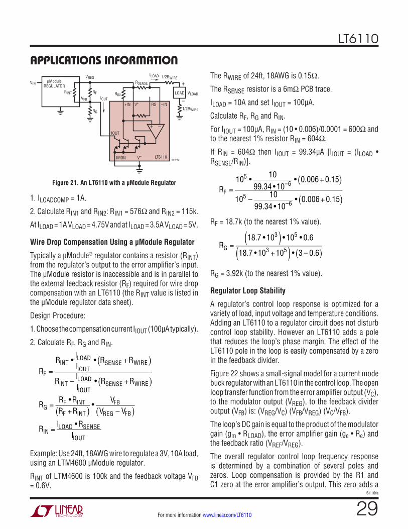
LT6110
296110fa
For more information www.linear.com/LT6110
applicaTions inForMaTion
1. ILOADCOMP = 1A.
2. Calculate RIN1 and RIN2: RIN1 = 576Ω and RIN2 = 115k.
At ILOAD = 1A VLOAD = 4.75V and at ILOAD = 3.5A VLOAD = 5V.
Wire Drop Compensation Using a µModule Regulator
Typically a µModule® regulator contains a resistor (RINT) from the regulator’s output to the error amplifier’s input. The µModule resistor is inaccessible and is in parallel to the external feedback resistor (RF) required for wire drop compensation with an LT6110 (the RINT value is listed in the µModule regulator data sheet).
Design Procedure:
1. Choose the compensation current IIOUT (100µA typically).
2. Calculate RF, RG and RIN.
RF =RINT • ILOAD
IIOUT• RSENSE +RWIRE( )
RINT – ILOADIIOUT
• RSENSE +RWIRE( )
RG =RF •RINTRF +RINT( )
• VFBVREG – VFB( )
RIN =ILOAD •RSENSE
IIOUT
Example: Use 24ft, 18AWG wire to regulate a 3V, 10A load, using an LTM4600 µModule regulator.
RINT of LTM4600 is 100k and the feedback voltage VFB = 0.6V.
The RWIRE of 24ft, 18AWG is 0.15Ω.
The RSENSE resistor is a 6mΩ PCB trace.
ILOAD = 10A and set IIOUT = 100µA.
Calculate RF, RG and RIN.
For IIOUT = 100µA, RIN = (10 • 0.006)/0.0001 = 600Ω and to the nearest 1% resistor RIN = 604Ω.
If RIN = 604Ω then IIOUT = 99.34µA [IIOUT = (ILOAD • RSENSE/RIN)].
RF =105 • 10
99.34 • 10–6 • 0.006+ 0.15( )
105 – 1099.34 • 10–6 • 0.006+ 0.15( )
RF = 18.7k (to the nearest 1% value).
RG =18.7 • 103( ) • 105 • 0.6
18.7 • 103 +105( ) • 3 – 0.6( )
RG = 3.92k (to the nearest 1% value).
Regulator Loop Stability
A regulator’s control loop response is optimized for a variety of load, input voltage and temperature conditions. Adding an LT6110 to a regulator circuit does not disturb control loop stability. However an LT6110 adds a pole that reduces the loop’s phase margin. The effect of the LT6110 pole in the loop is easily compensated by a zero in the feedback divider.
Figure 22 shows a small-signal model for a current mode buck regulator with an LT6110 in the control loop. The open loop transfer function from the error amplifier output (VC), to the modulator output (VREG), to the feedback divider output (VFB) is: (VREG/VC) (VFB/VREG) (VC/VFB).
The loop’s DC gain is equal to the product of the modulator gain (gm • RLOAD), the error amplifier gain (ge • Re) and the feedback ratio (VREF/VREG).
The overall regulator control loop frequency response is determined by a combination of several poles and zeros. Loop compensation is provided by the R1 and C1 zero at the error amplifier’s output. This zero adds a
Figure 21. An LT6110 with a µModule Regulator
VIN µModuleREGULATOR
RINT
IOUT
+IN –IN
RIN
LT6110
V+
V–
RS
RF
RG
IMON
+ –
VREG
VFB
ILOAD
IOUT
1/2RWIRE
6110 F21
RSENSE
VLOAD
+
–LOAD
1/2RWIRE
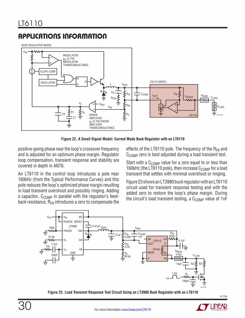
LT6110
306110fa
For more information www.linear.com/LT6110
applicaTions inForMaTion
positive-going phase near the loop’s crossover frequency and is adjusted for an optimum phase margin. Regulator loop compensation, transient response and stability are covered in depth in AN76.
An LT6110 in the control loop introduces a pole near 160kHz (from the Typical Performance Curves) and this pole reduces the loop’s optimized phase margin resulting in load transient overshoot and possibly ringing. Adding a capacitor, CCOMP in parallel with the regulator’s feed-back resistance, RFA introduces a zero to compensate the
effects of the LT6110 pole. The frequency of the RFA and CCOMP zero is best adjusted during a load transient test.
Start with a CCOMP value for a zero equal to or less than 160kHz (the LT6110 pole), then increase CCOMP for a load transient that settles with minimal overshoot or ringing.
Figure 23 shows an LT3980 buck regulator with an LT6110 circuit used for transient response testing and with the added zero to restore the loop’s phase margin. During the circuit’s load transient testing, a CCOMP value of 1nF
Figure 22. A Small-Signal Model: Current Mode Buck Regulator with an LT6110
Figure 23. Load Transient Response Test Circuit Using an LT3980 Buck Regulator with an LT6110
15k1.5nF
0.1µF
10µF
100pF
VINVIN BD
RUN/SS
0.47µF
47µF CCOMP1nF
VREG
RFA6.49k
RFB412k
10µHLT3980
GND
100k
RG80.6k
97.6k
BOOST
NC +IN
IOUTLT6110
V+
RSIMON
–INV–
20mΩ
PGOOD SW
RT DA
VC FB
6110 F23
1A180pF
1.6A 2k
RWIRE0.3Ω
RIN402Ω
5Ω 8Ω
VLOAD
VIN
CO CCOMPRFA
RFB
L
BUCK REGULATOR MODEL
RESR
VREFVFB
ERRORAMPLIFIERge IS THE ERRORAMPLIFIERTRANSCONDUCTANCE
MODULATORgm IS THEMODULATORTRANSCONDUCTANCE
VC
RQOSCILLATOR
SLOPE COMP
RG LT6110
LT6110 MODEL
R1 Re6110 F22
VLOAD
VREG
RWIRERSENSE
RLOAD
C1C2
IIOUT
+–
RIN
+–
+–
S
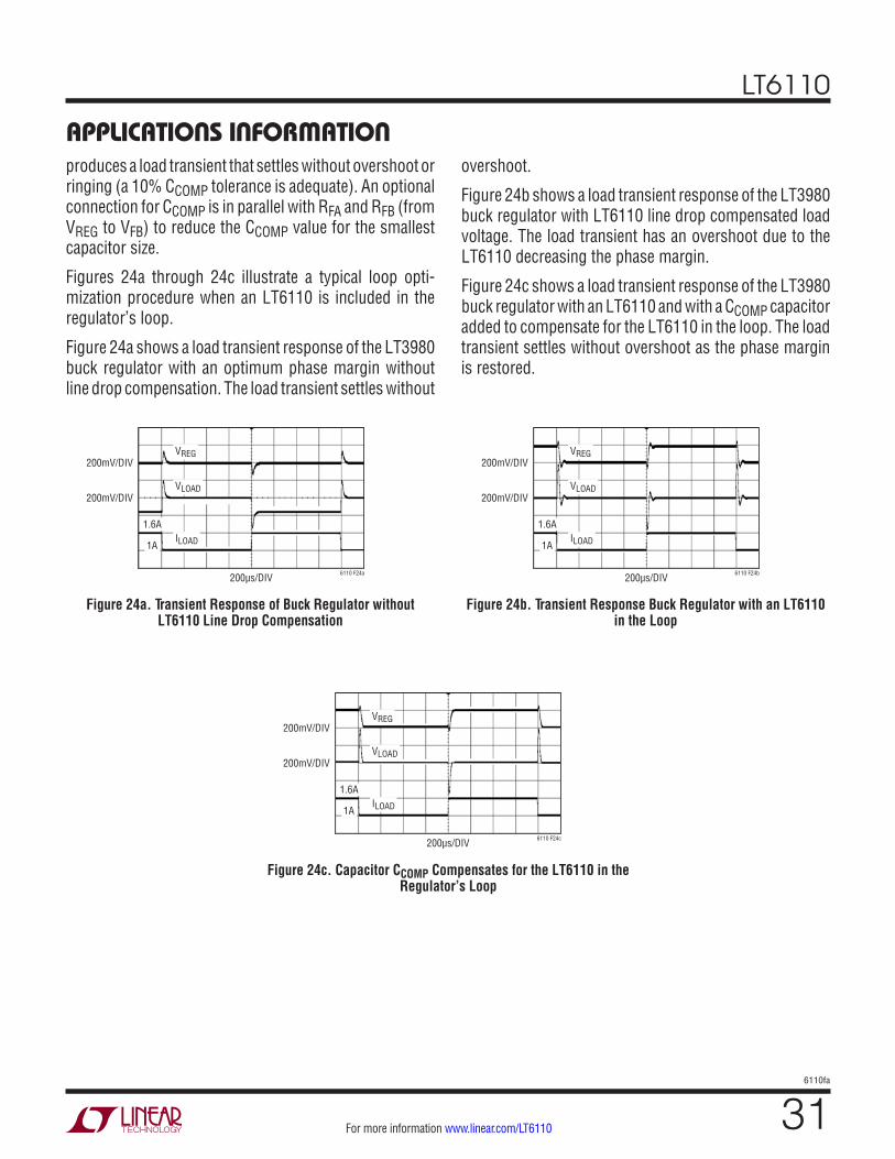
LT6110
316110fa
For more information www.linear.com/LT6110
applicaTions inForMaTion
Figure 24a. Transient Response of Buck Regulator without LT6110 Line Drop Compensation
Figure 24b. Transient Response Buck Regulator with an LT6110 in the Loop
produces a load transient that settles without overshoot or ringing (a 10% CCOMP tolerance is adequate). An optional connection for CCOMP is in parallel with RFA and RFB (from VREG to VFB) to reduce the CCOMP value for the smallest capacitor size.
Figures 24a through 24c illustrate a typical loop opti-mization procedure when an LT6110 is included in the regulator’s loop.
Figure 24a shows a load transient response of the LT3980 buck regulator with an optimum phase margin without line drop compensation. The load transient settles without
overshoot.
Figure 24b shows a load transient response of the LT3980 buck regulator with LT6110 line drop compensated load voltage. The load transient has an overshoot due to the LT6110 decreasing the phase margin.
Figure 24c shows a load transient response of the LT3980 buck regulator with an LT6110 and with a CCOMP capacitor added to compensate for the LT6110 in the loop. The load transient settles without overshoot as the phase margin is restored.
Figure 24c. Capacitor CCOMP Compensates for the LT6110 in the Regulator’s Loop
200mV/DIV
200mV/DIV
200µs/DIV 6110 F24a
VREG
VLOAD
ILOAD1A
1.6A
200mV/DIV
200mV/DIV
200µs/DIV 6110 F24b
VREG
VLOAD
ILOAD1A
1.6A
200mV/DIV
200mV/DIV
200µs/DIV 6110 F24c
VREG
VLOAD
ILOAD1A
1.6A
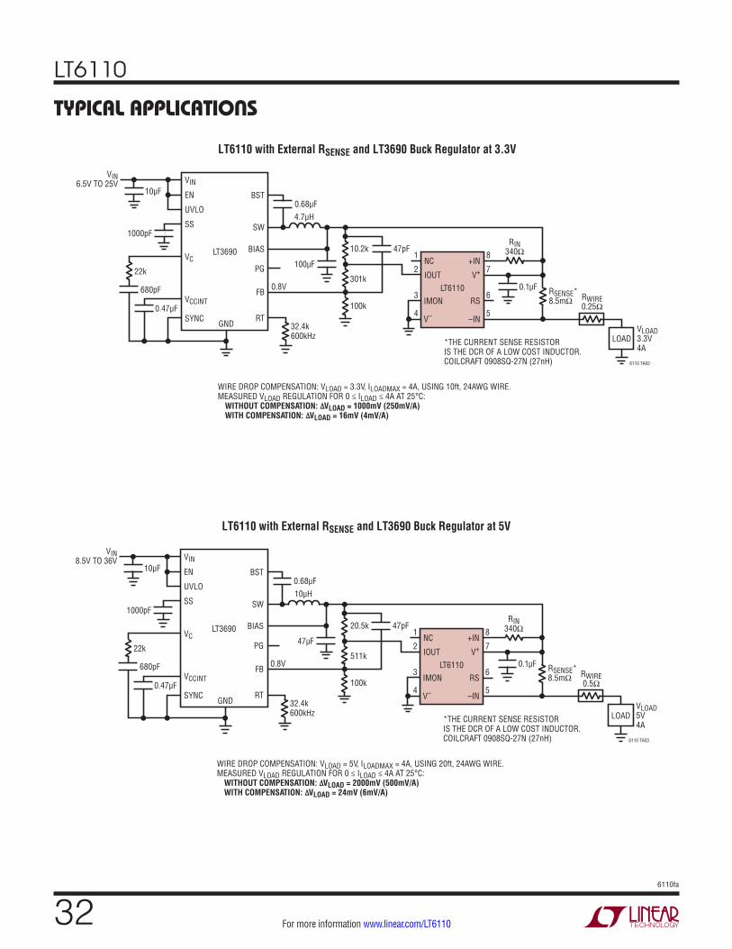
LT6110
326110fa
For more information www.linear.com/LT6110
Typical applicaTions
32.4k600kHz
VINVIN
6.5V TO 25V
UVLO
EN0.68µF
100µF
0.8V
47pF10.2k
301k
4.7µH
LT3690
GND
100k
NC +IN
IOUTLT6110
V+
RSIMON
–IN
8
7
6
5
1
2
3
4V–
BST
PG
BIAS
SW
VCCINT
22k
VC
SYNC
FB
RT
6110 TA02
VLOAD3.3V4A
0.1µF
10µF
0.47µF
SS1000pF
RWIRE0.25Ω
RSENSE*8.5mΩ
*THE CURRENT SENSE RESISTORIS THE DCR OF A LOW COST INDUCTOR.COILCRAFT 0908SQ-27N (27nH)
WIRE DROP COMPENSATION: VLOAD = 3.3V, ILOADMAX = 4A, USING 10ft, 24AWG WIRE.MEASURED VLOAD REGULATION FOR 0 ≤ ILOAD ≤ 4A AT 25°C: WITHOUT COMPENSATION: ∆VLOAD = 1000mV (250mV/A) WITH COMPENSATION: ∆VLOAD = 16mV (4mV/A)
RIN340Ω
LOAD
680pF
LT6110 with External RSENSE and LT3690 Buck Regulator at 3.3V
32.4k600kHz
VINVIN
8.5V TO 36V
UVLO
EN0.68µF
47µF
0.8V
47pF20.5k
511k
10µH
LT3690
GND
100k
NC +IN
IOUTLT6110
V+
RSIMON
–IN
8
7
6
5
1
2
3
4V–
BST
PG
BIAS
SW
VCCINT
22k
VC
SYNC
FB
RT
6110 TA03
VLOAD5V4A
0.1µF
10µF
0.47µF
SS1000pF
RWIRE0.5Ω
RSENSE*8.5mΩ
*THE CURRENT SENSE RESISTORIS THE DCR OF A LOW COST INDUCTOR.COILCRAFT 0908SQ-27N (27nH)
WIRE DROP COMPENSATION: VLOAD = 5V, ILOADMAX = 4A, USING 20ft, 24AWG WIRE.MEASURED VLOAD REGULATION FOR 0 ≤ ILOAD ≤ 4A AT 25°C: WITHOUT COMPENSATION: ∆VLOAD = 2000mV (500mV/A) WITH COMPENSATION: ∆VLOAD = 24mV (6mV/A)
RIN340Ω
LOAD
680pF
LT6110 with External RSENSE and LT3690 Buck Regulator at 5V
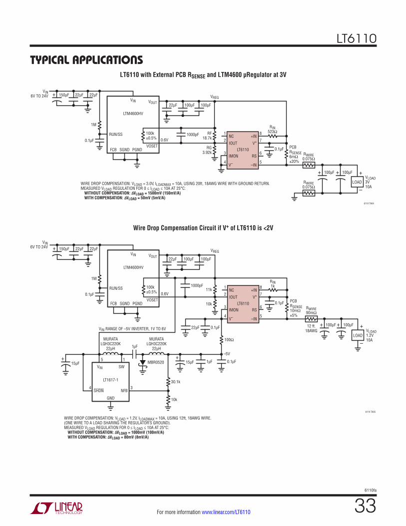
LT6110
336110fa
For more information www.linear.com/LT6110
Typical applicaTionsLT6110 with External PCB RSENSE and LTM4600 µRegulator at 3V
Wire Drop Compensation Circuit if V+ of LT6110 is <2V
RF18.7k0.6V
RG3.92k
NC +IN
IOUTLT6110
V+
RSIMON
–IN
8
7
6
5
1
2
3
4V–
6110 TA04
VLOAD3V10A
0.1µFRWIRE
0.075Ω
PCBRSENSE6mΩ±20%
WIRE DROP COMPENSATION: VLOAD = 3.0V, ILOADMAX = 10A, USING 20ft, 18AWG WIRE WITH GROUND RETURN.MEASURED VLOAD REGULATION FOR 0 ≤ ILOAD ≤ 10A AT 25°C: WITHOUT COMPENSATION: ∆VLOAD = 1500mV (150mV/A) WITH COMPENSATION: ∆VLOAD = 50mV (5mV/A)
RIN523Ω
RWIRE0.075Ω
RUN/SS
VOUT
VREG
FCB SGND PGNDVOSET
0.1µF
VIN6V TO 24V 22µF22µF150µF
1M
100k±0.5%
VIN
LTM4600HV
+
22µF 100µF 100µF
1000pF
+
–LOAD
100µF+ 100µF+
11k0.6V
10k
NC +IN
IOUTLT6110
V+
RSIMON
–IN
8
7
6
5
1
2
3
4V–
6110 TA05
VLOAD1.2V10A
0.1µFRWIRE90mΩ
12 ft.18AWG
WIRE DROP COMPENSATION: VLOAD = 1.2V, ILOADMAX = 10A, USING 12ft, 18AWG WIRE.(ONE WIRE TO A LOAD SHARING THE REGULATOR’S GROUND).MEASURED VLOAD REGULATION FOR 0 ≤ ILOAD ≤ 10A AT 25°C: WITHOUT COMPENSATION: ∆VLOAD = 1000mV (100mV/A) WITH COMPENSATION: ∆VLOAD = 80mV (8mV/A)
RIN1kRUN/SS
VIN RANGE OF –5V INVERTER, 1V TO 6V
VOUT
VREG
FCB SGND PGNDVOSET
0.1µF
VIN6V TO 24V 22µF22µF150µF
1M
100k±0.5%
VIN
LTM4600HV
+
22µF 100µF 100µF
1000pF
22µF +
–LOAD
100µF+ 100µF+
PCBRSENSE10mΩ±5%
LT1617-1
GND
MURATALQH3C220K
22µH
VIN SW
SHDN NFB4 3
0.1µF
1µF 0.1µFMBR0520
MURATALQH3C220K
22µH1µF
1515µF
+15µF
+
30.1k
10k
100Ω
–5V
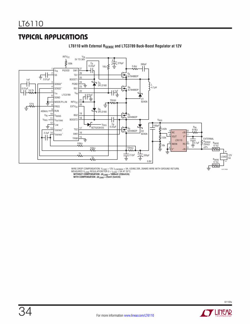
LT6110
346110fa
For more information www.linear.com/LT6110
Typical applicaTionsLT6110 with External RSENSE and LTC3789 Buck-Boost Regulator at 12V
6110 TA06
12V5A
RWIRE0.1Ω
RWIRE0.1Ω
+
–LOAD
5.62k
133k
10k
100k
NC +IN
IOUTLT6110
V+
RSIMON
–IN
8
7
6
5
1
2
3
4V–
0.1µF
100pF
2.2µF
WIRE DROP COMPENSATION: VLOAD = 12V, ILOADMAX = 5A, USING 20ft, 20AWG WIRE WITH GROUND RETURN.MEASURED VLOAD REGULATION FOR 0 ≤ ILOAD ≤ 5A AT 25°C: WITHOUT COMPENSATION: ∆VLOAD = 1000mV (250mV/A) WITH COMPENSATION: ∆VLOAD = 25mV (5mV/A)
RIN619Ω
EXTERNALRSENSE25mΩ±5%
LTC3789
DADFLS160
DBDFLS160
QASi7848BDP
QBSi7848BDP
D1B240A
1µF
330µF
VREG
VIN
VREG
VIN5V TO 36V
0.01µF
1nF 0.01µF
CA0.22µF
INTVCC
CB0.22µF
10mΩ
QCSiR496DP
L4.7µH
QDSiR496DP
VFB
SS
SENSE+
SENSE–
ITH
SGND
MODE/PLLIN
FREQ
RUN
VINSNS
VOUTSNS
ILIM VREGBZT52C6V2S
PGOOD SW1
TG1
BOOST1
PGND
BG1
VIN
INTVCC
EXTVCC
1
2
3
4
5
6
27
26
25
24
23
22
BG2
BOOST2
IOSENSE+
IOSENSE–
TG2
SW2
TRIM
7
8
9
10
11
12
13
14
21
20
19
18
17
16
15
1k
400kHz
0.8V
14.7k
121k
390pF
D2B240A
10mΩ
5.6Ω10Ω
1k
100Ω
100Ω
2.2µF
+
10µF
270µF+
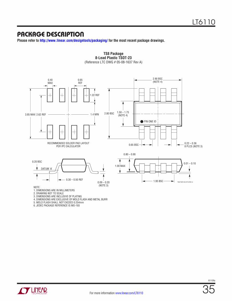
LT6110
356110fa
For more information www.linear.com/LT6110
package DescripTionPlease refer to http://www.linear.com/designtools/packaging/ for the most recent package drawings.
1.50 – 1.75(NOTE 4)
2.80 BSC
0.22 – 0.36 8 PLCS (NOTE 3)
DATUM ‘A’
0.09 – 0.20(NOTE 3)
TS8 TSOT-23 0710 REV A
2.90 BSC(NOTE 4)
0.65 BSC
1.95 BSC
0.80 – 0.90
1.00 MAX0.01 – 0.10
0.20 BSC
0.30 – 0.50 REF
PIN ONE ID
NOTE:1. DIMENSIONS ARE IN MILLIMETERS2. DRAWING NOT TO SCALE3. DIMENSIONS ARE INCLUSIVE OF PLATING4. DIMENSIONS ARE EXCLUSIVE OF MOLD FLASH AND METAL BURR5. MOLD FLASH SHALL NOT EXCEED 0.254mm6. JEDEC PACKAGE REFERENCE IS MO-193
3.85 MAX
0.40MAX
0.65REF
RECOMMENDED SOLDER PAD LAYOUTPER IPC CALCULATOR
1.4 MIN2.62 REF
1.22 REF
TS8 Package8-Lead Plastic TSOT-23
(Reference LTC DWG # 05-08-1637 Rev A)
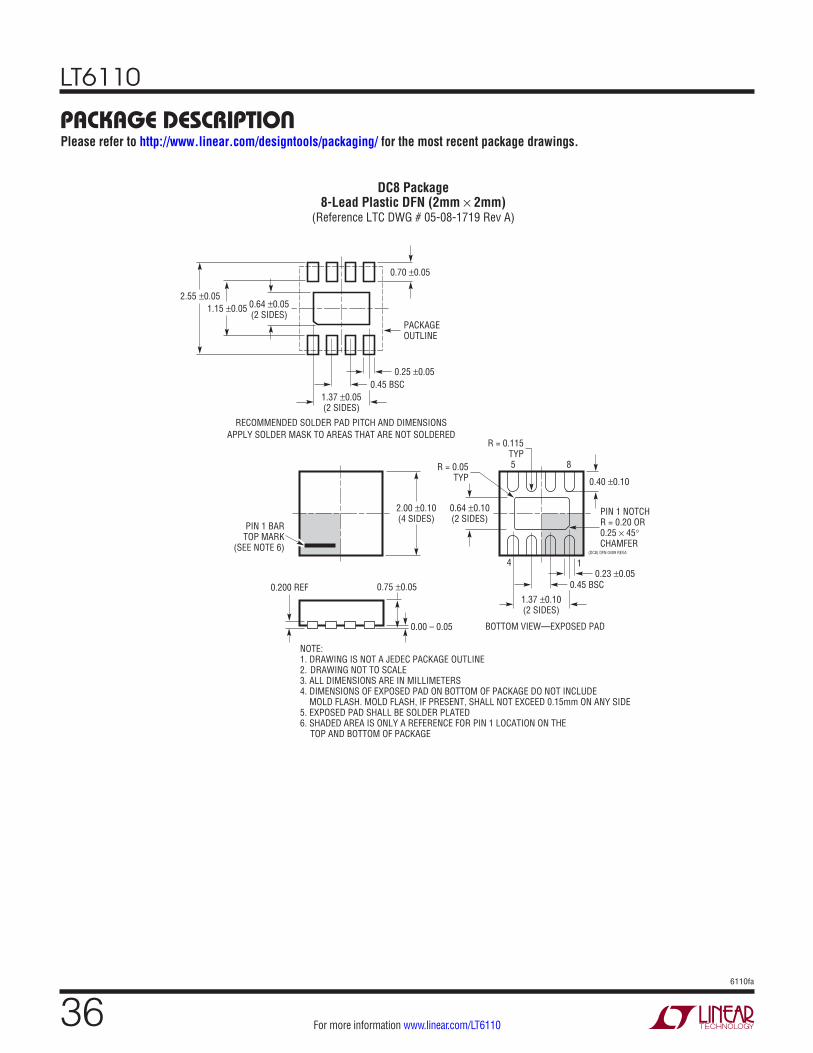
LT6110
366110fa
For more information www.linear.com/LT6110
package DescripTionPlease refer to http://www.linear.com/designtools/packaging/ for the most recent package drawings.
2.00 ±0.10(4 SIDES)
NOTE:1. DRAWING IS NOT A JEDEC PACKAGE OUTLINE2. DRAWING NOT TO SCALE3. ALL DIMENSIONS ARE IN MILLIMETERS4. DIMENSIONS OF EXPOSED PAD ON BOTTOM OF PACKAGE DO NOT INCLUDE MOLD FLASH. MOLD FLASH, IF PRESENT, SHALL NOT EXCEED 0.15mm ON ANY SIDE5. EXPOSED PAD SHALL BE SOLDER PLATED 6. SHADED AREA IS ONLY A REFERENCE FOR PIN 1 LOCATION ON THE TOP AND BOTTOM OF PACKAGE
0.40 ±0.10
BOTTOM VIEW—EXPOSED PAD
0.64 ±0.10(2 SIDES)
0.75 ±0.05
R = 0.115TYP
R = 0.05TYP
1.37 ±0.10(2 SIDES)
14
85
PIN 1 BARTOP MARK
(SEE NOTE 6)
0.200 REF
0.00 – 0.05
(DC8) DFN 0409 REVA
0.23 ±0.050.45 BSC
0.25 ±0.05
1.37 ±0.05(2 SIDES)
RECOMMENDED SOLDER PAD PITCH AND DIMENSIONSAPPLY SOLDER MASK TO AREAS THAT ARE NOT SOLDERED
0.64 ±0.05(2 SIDES)
1.15 ±0.05
0.70 ±0.05
2.55 ±0.05
PACKAGEOUTLINE
0.45 BSC
PIN 1 NOTCH R = 0.20 OR 0.25 × 45° CHAMFER
DC8 Package8-Lead Plastic DFN (2mm × 2mm)
(Reference LTC DWG # 05-08-1719 Rev A)
LT6110
376110fa
For more information www.linear.com/LT6110
Information furnished by Linear Technology Corporation is believed to be accurate and reliable. However, no responsibility is assumed for its use. Linear Technology Corporation makes no representa-tion that the interconnection of its circuits as described herein will not infringe on existing patent rights.
revision hisToryREV DATE DESCRIPTION PAGE NUMBER
A 11/13 Maximum Amplifier Bias Current changed from 200nA to 100nAAddition of Minimum Input Voltage graphEdits to Compensating an Output Referred Adjustable Voltage Regulator sectionEdits to Error Sources sectionTitle added – Wire Drop Compensation Using a Micromodule RegulatorEdits to schematic LT6110 with External PCB RSENSE and LTM4600 µModule Regulator at 3VReplaced schematic LT6110 with External PCB RSENSE and LTM4600 µModule Regulator at 1.8V with new circuit, Wire Drop Compensation Circuit if V+ of LT6110 < 2VEdits to schematic LT6110 with Internal RSENSE and LT3975 Buck Regulator at 3.3V
37
1618, 19, 20
293333
38

LT6110
386110fa
For more information www.linear.com/LT6110 LINEAR TECHNOLOGY CORPORATION 2013
LT 1113 REV A • PRINTED IN USALinear Technology Corporation1630 McCarthy Blvd., Milpitas, CA 95035-7417(408) 432-1900 FAX: (408) 434-0507 www.linear.com/LT6110
relaTeD parTs
Typical applicaTion
PART NUMBER DESCRIPTION COMMENTS
LT1787 Bidirectional High Side Current Sense Amplifier 2.7V to 60V, 75µV Offset, 60µA Quiescent, 8V/V Gain
LTC4150 Coulomb Counter/Battery Gas Gauge Indicates Charge Quantity and Polarity
LT6100 Gain-Selectable High Side Current Sense Amplifier 4.1V to 48V, Gain Settings: 10, 12.5, 20, 25, 40, 50V/V
LTC6101 High Voltage High Side Current Sense Amplifier Up to 100V, Resistor Set Gain, 300µV Offset, SOT-23
LTC6102 Zero Drift High Side Current Sense Amplifier Up to 100V, Resistor Set Gain, 10µV Offset, MSOP8/DFN
LTC6103 Dual High Side Current Sense Amplifier 4V TO 60V, Resistor Set Gain, 2 Independent Amps, MSOP8
LTC6104 Bidirectional High Side Current Sense Amplifier 4V TO 60V, Separate Gain Control for Each Direction, MSOP8
LT6105 Precision Rail-to-Rail Input Current Sense Amplifier –0.3V to 44V Input Range, 300µV Offset, 1% Gain Error
LT6106 Low Cost High Side Current Sense Amplifier 2.7V to 36V, 250µV Offset, Resistor Set Gain, SOT23
LT6107 High Temperature High Side Current Sense Amplifier 2.7V to 36V, –55°C 150°C, Fully Tested: –55°C, 25°C, 150°C
LT6700 Dual Comparator with 400mV Reference 1.4V to 18V, 6.5µA Supply Current
LT4180 Virtual Remote Sense Controller Automatically Detects Line Impedance to Improve Load Regulation
LT6110 with Internal RSENSE and LT3975 Buck Regulator at 3.3V
0.47µF
100µF
1.197V
16.5k
1M
4.7µH
LT3975
GND576k
NC +IN
IOUTLT6110
V+
RSIMON
–IN
8
7
6
5
1
2
3
4V–
B00ST
OUT
SW
SS
RTSYNC
FB
1µF
10pF
6110 TA07
0.1µF10nF
RWIRE0.32Ω
WIRE DROP COMPENSATION: VLOAD = 3.3V, ILOADMAX = 2.5A, USING 6ft, 30AWG WIRE WITH GROUND RETURN.MEASURED VLOAD REGULATION FOR 0 ≤ ILOAD ≤ 2.5A AT 25°C: WITHOUT COMPENSATION: ∆VLOAD = 1600mV (640mV/A) WITH COMPENSATION: ∆VLOAD = 25mV (10mV/A)
RIN499Ω
VLOAD3.3V2.5A
VREG
RWIRE0.32Ω
+
–LOAD
VINVIN
7V TO 42V
EN
PDS360
100µF 10µF
78.7kf = 600kHz
Related Documents