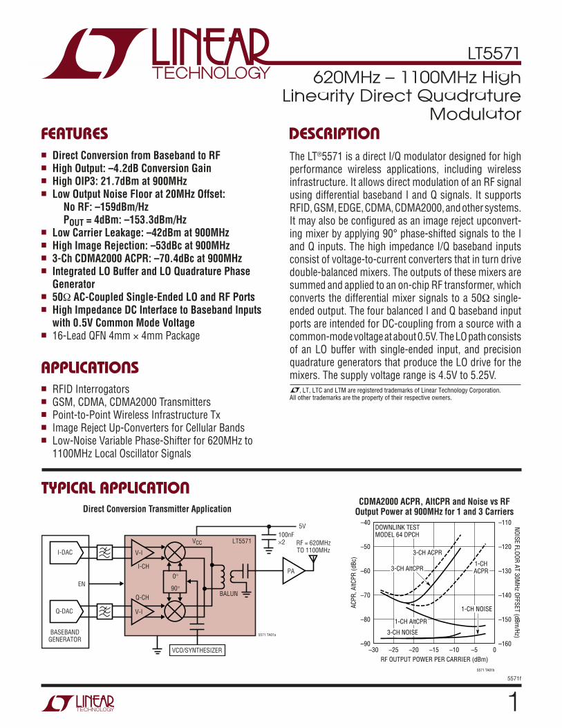
LT5571 1 5571f RF OUTPUT POWER PER CARRIER (dBm) –30 ACPR, AltCPR (dBc) NOISE FLOOR AT 30MHz OFFSET (dBm/Hz) –70 –60 –10 5571 TA01b –80 –90 –25 –20 –15 0 –5 –40 –50 –140 –130 –150 –160 –110 –120 DOWNLINK TEST MODEL 64 DPCH 3-CH ACPR 1-CH ACPR 3-CH AltCPR 1-CH AltCPR 3-CH NOISE 1-CH NOISE TYPICAL APPLICATION FEATURES APPLICATIONS DESCRIPTION 620MHz – 1100MHz High Linearity Direct Quadrature Modulator The LT ® 5571 is a direct I/Q modulator designed for high performance wireless applications, including wireless infrastructure. It allows direct modulation of an RF signal using differential baseband I and Q signals. It supports RFID, GSM, EDGE, CDMA, CDMA2000, and other systems. It may also be configured as an image reject upconvert- ing mixer by applying 90° phase-shifted signals to the I and Q inputs. The high impedance I/Q baseband inputs consist of voltage-to-current converters that in turn drive double-balanced mixers. The outputs of these mixers are summed and applied to an on-chip RF transformer, which converts the differential mixer signals to a 50Ω single- ended output. The four balanced I and Q baseband input ports are intended for DC-coupling from a source with a common-mode voltage at about 0.5V. The LO path consists of an LO buffer with single-ended input, and precision quadrature generators that produce the LO drive for the mixers. The supply voltage range is 4.5V to 5.25V. Direct Conversion Transmitter Application ■ Direct Conversion from Baseband to RF ■ High Output: –4.2dB Conversion Gain ■ High OIP3: 21.7dBm at 900MHz ■ Low Output Noise Floor at 20MHz Offset: No RF: –159dBm/Hz P OUT = 4dBm: –153.3dBm/Hz ■ Low Carrier Leakage: –42dBm at 900MHz ■ High Image Rejection: –53dBc at 900MHz ■ 3-Ch CDMA2000 ACPR: –70.4dBc at 900MHz ■ Integrated LO Buffer and LO Quadrature Phase Generator ■ 50Ω AC-Coupled Single-Ended LO and RF Ports ■ High Impedance DC Interface to Baseband Inputs with 0.5V Common Mode Voltage ■ 16-Lead QFN 4mm 4mm Package ■ RFID Interrogators ■ GSM, CDMA, CDMA2000 Transmitters ■ Point-to-Point Wireless Infrastructure Tx ■ Image Reject Up-Converters for Cellular Bands ■ Low-Noise Variable Phase-Shifter for 620MHz to 1100MHz Local Oscillator Signals , LT, LTC and LTM are registered trademarks of Linear Technology Corporation. All other trademarks are the property of their respective owners. CDMA2000 ACPR, AltCPR and Noise vs RF Output Power at 900MHz for 1 and 3 Carriers VCO/SYNTHESIZER EN I-CH Q-CH BALUN V CC V-I BASEBAND GENERATOR V-I LT5571 5V 5571 TA01a PA RF = 620MHz TO 1100MHz I-DAC Q-DAC 90° 0° 100nF ×2

Welcome message from author
This document is posted to help you gain knowledge. Please leave a comment to let me know what you think about it! Share it to your friends and learn new things together.
Transcript
LT5571
15571f
RF OUTPUT POWER PER CARRIER (dBm)–30
ACPR
, AltC
PR (d
Bc)
NOISE FLOOR AT 30MHz OFFSET (dBm
/Hz)
–70
–60
–10
5571 TA01b
–80
–90–25 –20 –15 0–5
–40
–50
–140
–130
–150
–160
–110
–120
DOWNLINK TESTMODEL 64 DPCH
3-CH ACPR
1-CHACPR3-CH AltCPR
1-CH AltCPR
3-CH NOISE
1-CH NOISE
TYPICAL APPLICATION
FEATURES
APPLICATIONS
DESCRIPTION
620MHz – 1100MHz High Linearity Direct Quadrature
Modulator
The LT®5571 is a direct I/Q modulator designed for high performance wireless applications, including wireless infrastructure. It allows direct modulation of an RF signal using differential baseband I and Q signals. It supports RFID, GSM, EDGE, CDMA, CDMA2000, and other systems. It may also be confi gured as an image reject upconvert-ing mixer by applying 90° phase-shifted signals to the I and Q inputs. The high impedance I/Q baseband inputs consist of voltage-to-current converters that in turn drive double-balanced mixers. The outputs of these mixers are summed and applied to an on-chip RF transformer, which converts the differential mixer signals to a 50Ω single-ended output. The four balanced I and Q baseband input ports are intended for DC-coupling from a source with a common-mode voltage at about 0.5V. The LO path consists of an LO buffer with single-ended input, and precision quadrature generators that produce the LO drive for the mixers. The supply voltage range is 4.5V to 5.25V.
Direct Conversion Transmitter Application
Direct Conversion from Baseband to RF High Output: –4.2dB Conversion Gain High OIP3: 21.7dBm at 900MHz Low Output Noise Floor at 20MHz Offset:
No RF: –159dBm/Hz POUT = 4dBm: –153.3dBm/Hz
Low Carrier Leakage: –42dBm at 900MHz High Image Rejection: –53dBc at 900MHz 3-Ch CDMA2000 ACPR: –70.4dBc at 900MHz Integrated LO Buffer and LO Quadrature Phase
Generator 50Ω AC-Coupled Single-Ended LO and RF Ports High Impedance DC Interface to Baseband Inputs
with 0.5V Common Mode Voltage 16-Lead QFN 4mm × 4mm Package
RFID Interrogators GSM, CDMA, CDMA2000 Transmitters Point-to-Point Wireless Infrastructure Tx Image Reject Up-Converters for Cellular Bands Low-Noise Variable Phase-Shifter for 620MHz to
1100MHz Local Oscillator Signals
, LT, LTC and LTM are registered trademarks of Linear Technology Corporation. All other trademarks are the property of their respective owners.
CDMA2000 ACPR, AltCPR and Noise vs RF Output Power at 900MHz for 1 and 3 Carriers
VCO/SYNTHESIZER
EN
I-CH
Q-CH BALUN
VCC
V-I
BASEBANDGENERATOR
V-I
LT5571
5V
5571 TA01a
PA
RF = 620MHzTO 1100MHzI-DAC
Q-DAC
90°
0°
100nF×2
LT5571
25571f
PACKAGE/ORDER INFORMATION
ELECTRICAL CHARACTERISTICS
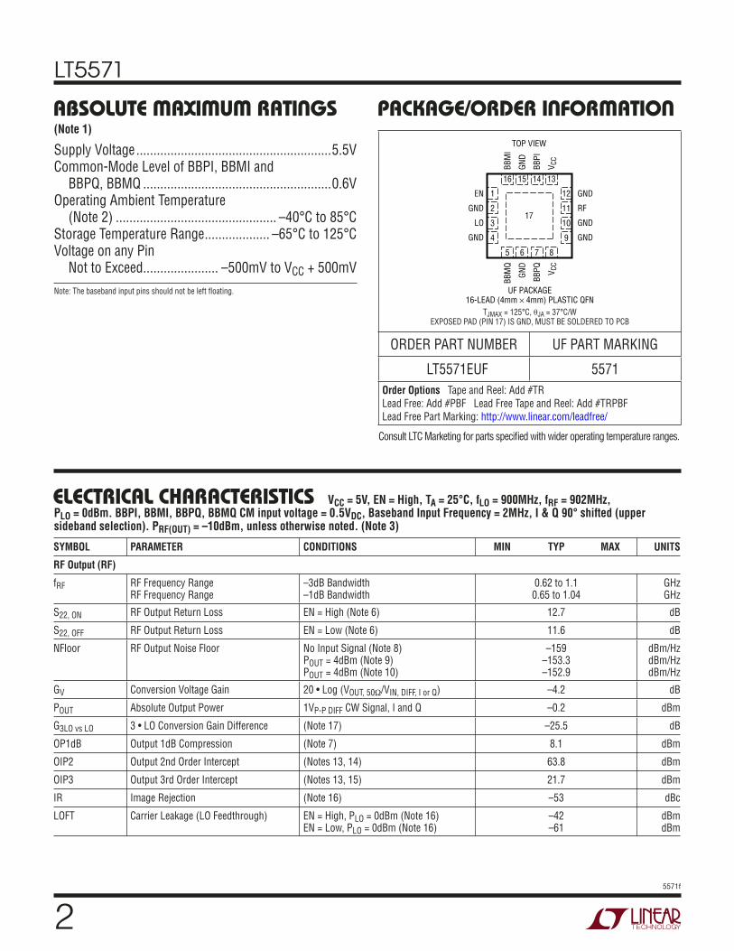
ABSOLUTE MAXIMUM RATINGS
Supply Voltage .........................................................5.5VCommon-Mode Level of BBPI, BBMI and
BBPQ, BBMQ .......................................................0.6VOperating Ambient Temperature
(Note 2) ............................................... –40°C to 85°CStorage Temperature Range ................... –65°C to 125°CVoltage on any Pin
Not to Exceed ...................... –500mV to VCC + 500mV
(Note 1)
16 15 14 13
5 6 7 8
TOP VIEW
17
UF PACKAGE16-LEAD (4mm × 4mm) PLASTIC QFN
9
10
11
12
4
3
2
1EN
GND
LO
GND
GND
RF
GND
GND
BBM
I
GND
BBPI
V CC
BBM
Q
GND
BBPQ V C
C
TJMAX = 125°C, θJA = 37°C/WEXPOSED PAD (PIN 17) IS GND, MUST BE SOLDERED TO PCB
ORDER PART NUMBER UF PART MARKING
LT5571EUF 5571Order Options Tape and Reel: Add #TRLead Free: Add #PBF Lead Free Tape and Reel: Add #TRPBFLead Free Part Marking: http://www.linear.com/leadfree/
Consult LTC Marketing for parts specifi ed with wider operating temperature ranges.
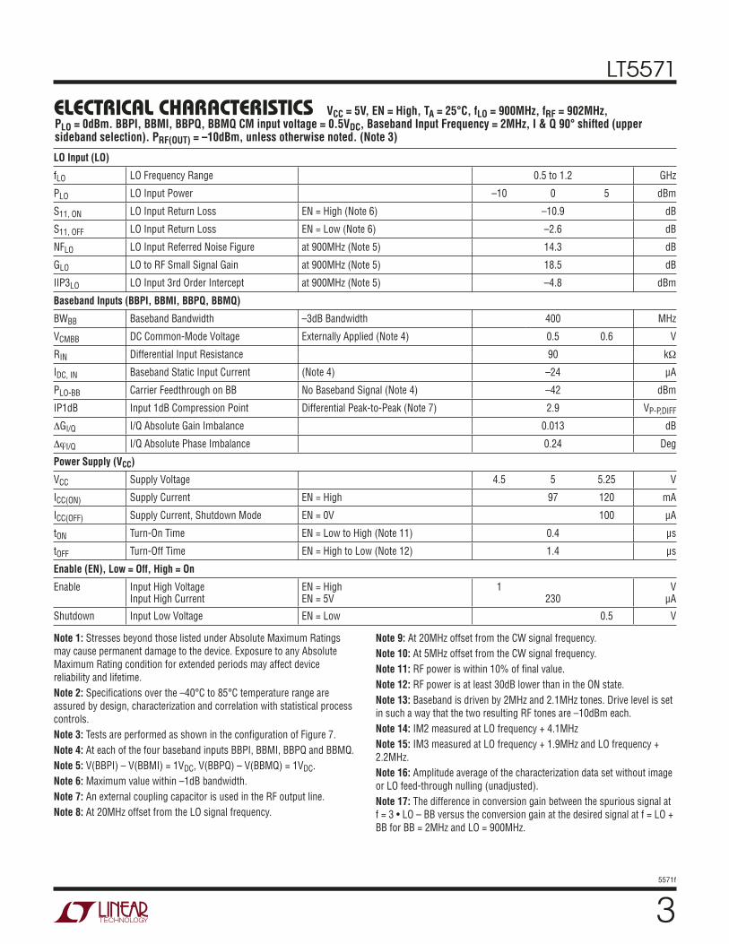
VCC = 5V, EN = High, TA = 25°C, fLO = 900MHz, fRF = 902MHz, PLO = 0dBm. BBPI, BBMI, BBPQ, BBMQ CM input voltage = 0.5VDC, Baseband Input Frequency = 2MHz, I & Q 90° shifted (upper sideband selection). PRF(OUT) = –10dBm, unless otherwise noted. (Note 3)
SYMBOL PARAMETER CONDITIONS MIN TYP MAX UNITS
RF Output (RF)
fRF RF Frequency RangeRF Frequency Range
–3dB Bandwidth–1dB Bandwidth
0.62 to 1.10.65 to 1.04
GHzGHz
S22, ON RF Output Return Loss EN = High (Note 6) 12.7 dB
S22, OFF RF Output Return Loss EN = Low (Note 6) 11.6 dB
NFloor RF Output Noise Floor No Input Signal (Note 8)POUT = 4dBm (Note 9)POUT = 4dBm (Note 10)
–159–153.3–152.9
dBm/HzdBm/HzdBm/Hz
GV Conversion Voltage Gain 20 • Log (VOUT, 50Ω/VIN, DIFF, I or Q) –4.2 dB
POUT Absolute Output Power 1VP-P DIFF CW Signal, I and Q –0.2 dBm
G3LO vs LO 3 • LO Conversion Gain Difference (Note 17) –25.5 dB
OP1dB Output 1dB Compression (Note 7) 8.1 dBm
OIP2 Output 2nd Order Intercept (Notes 13, 14) 63.8 dBm
OIP3 Output 3rd Order Intercept (Notes 13, 15) 21.7 dBm
IR Image Rejection (Note 16) –53 dBc
LOFT Carrier Leakage (LO Feedthrough) EN = High, PLO = 0dBm (Note 16)EN = Low, PLO = 0dBm (Note 16)
–42–61
dBmdBm
Note: The baseband input pins should not be left fl oating.
LT5571
35571f
Note 1: Stresses beyond those listed under Absolute Maximum Ratings may cause permanent damage to the device. Exposure to any Absolute Maximum Rating condition for extended periods may affect device reliability and lifetime.Note 2: Specifi cations over the –40°C to 85°C temperature range are assured by design, characterization and correlation with statistical process controls.Note 3: Tests are performed as shown in the confi guration of Figure 7.Note 4: At each of the four baseband inputs BBPI, BBMI, BBPQ and BBMQ.Note 5: V(BBPI) – V(BBMI) = 1VDC, V(BBPQ) – V(BBMQ) = 1VDC.Note 6: Maximum value within –1dB bandwidth.Note 7: An external coupling capacitor is used in the RF output line.Note 8: At 20MHz offset from the LO signal frequency.
LO Input (LO)
fLO LO Frequency Range 0.5 to 1.2 GHz
PLO LO Input Power –10 0 5 dBm
S11, ON LO Input Return Loss EN = High (Note 6) –10.9 dB
S11, OFF LO Input Return Loss EN = Low (Note 6) –2.6 dB
NFLO LO Input Referred Noise Figure at 900MHz (Note 5) 14.3 dB
GLO LO to RF Small Signal Gain at 900MHz (Note 5) 18.5 dB
IIP3LO LO Input 3rd Order Intercept at 900MHz (Note 5) –4.8 dBm
Baseband Inputs (BBPI, BBMI, BBPQ, BBMQ)
BWBB Baseband Bandwidth –3dB Bandwidth 400 MHz
VCMBB DC Common-Mode Voltage Externally Applied (Note 4) 0.5 0.6 V
RIN Differential Input Resistance 90 kΩ
IDC, IN Baseband Static Input Current (Note 4) –24 µA
PLO-BB Carrier Feedthrough on BB No Baseband Signal (Note 4) –42 dBm
IP1dB Input 1dB Compression Point Differential Peak-to-Peak (Note 7) 2.9 VP-P,DIFF
ΔGI/Q I/Q Absolute Gain Imbalance 0.013 dB
ΔϕI/Q I/Q Absolute Phase Imbalance 0.24 Deg
Power Supply (VCC)
VCC Supply Voltage 4.5 5 5.25 V
ICC(ON) Supply Current EN = High 97 120 mA
ICC(OFF) Supply Current, Shutdown Mode EN = 0V 100 µA
tON Turn-On Time EN = Low to High (Note 11) 0.4 µs
tOFF Turn-Off Time EN = High to Low (Note 12) 1.4 µs
Enable (EN), Low = Off, High = On
Enable Input High VoltageInput High Current
EN = HighEN = 5V
1230
VµA
Shutdown Input Low Voltage EN = Low 0.5 V
ELECTRICAL CHARACTERISTICS VCC = 5V, EN = High, TA = 25°C, fLO = 900MHz, fRF = 902MHz, PLO = 0dBm. BBPI, BBMI, BBPQ, BBMQ CM input voltage = 0.5VDC, Baseband Input Frequency = 2MHz, I & Q 90° shifted (upper sideband selection). PRF(OUT) = –10dBm, unless otherwise noted. (Note 3)
Note 9: At 20MHz offset from the CW signal frequency.Note 10: At 5MHz offset from the CW signal frequency.Note 11: RF power is within 10% of fi nal value.Note 12: RF power is at least 30dB lower than in the ON state.Note 13: Baseband is driven by 2MHz and 2.1MHz tones. Drive level is set in such a way that the two resulting RF tones are –10dBm each.Note 14: IM2 measured at LO frequency + 4.1MHzNote 15: IM3 measured at LO frequency + 1.9MHz and LO frequency + 2.2MHz.Note 16: Amplitude average of the characterization data set without image or LO feed-through nulling (unadjusted).Note 17: The difference in conversion gain between the spurious signal at f = 3 • LO – BB versus the conversion gain at the desired signal at f = LO + BB for BB = 2MHz and LO = 900MHz.

LT5571
45571f
2 • LO FREQUENCY (GHz)1.1
2 • L
O LE
AKAG
E (d
Bm)
–40
2.3 2.5
5571 G08
–45
–50
1.3 1.5 1.7 2.11.9
–55
–60
5V, –40°C5V, 25°C5V, 85°C4.5V, 25°C5.5V, 25°C
LO FREQUENCY (MHz)550
LO F
EEDT
HROU
GH (d
Bm) –42
1150 1250
5571 G07
–44
650 750 850 1050950
–46
–48
–40
5V, –40°C5V, 25°C5V, 85°C4.5V, 25°C5.5V, 25°C
3 • LO FREQUENCY (GHz)1.65
3 • L
O LE
AKAG
E (d
Bm)
–50
–45
3.5 3.75
5571 G09
–55
–60
1.95 2.25 2.55 3.152.85
–65
–70
5V, –40°C5V, 25°C5V, 85°C4.5V, 25°C5.5V, 25°C
LO FREQUENCY (MHz)550
OP1d
B (d
Bm) 6
8
1150 1250
5571 G06
4
2
650 750 850 1050950
0
–2
10
5V, –40°C5V, 25°C5V, 85°C4.5V, 25°C5.5V, 25°C
LO FREQUENCY (MHz)550
OIP3
(dBm
)
20
22
24
1150 1250
5571 G04
18
16
650 750 850 1050950
14
12
26fBB, 1 = 2MHzfBB, 2 = 2.1MHz
5V, –40°C5V, 25°C5V, 85°C4.5V, 25°C5.5V, 25°C
LO FREQUENCY (MHz)550
VOLT
AGE
GAIN
(dB)
–8
–6
–4
1150 1250
5558 G03
–10
–12
650 750 850 1050950
–14
–16
–2
5V, –40°C5V, 25°C5V, 85°C4.5V, 25°C5.5V, 25°C
SUPPLY VOLTAGE (V)4.50
80
90
SUPP
LY C
URRE
NT (m
A)
100
110
85°C
25°C
–40°C
5.004.75
5571 G01
5.25LO FREQUENCY (MHz)
550
RF O
UTPU
T PO
WER
(dBm
)–4
–2
0
1150 1250
5571 G02
–6
–8
650 750 850 1050950
–10
–12
2
5V, –40°C5V, 25°C5V, 85°C4.5V, 25°C5.5V, 25°C
LO FREQUENCY (MHz)550
OIP2
(dBm
)
65
70
1150 1250
5571 G05
60
55
650 750 850 1050950
50
45
75fIM2 = fBB, 1 + fBB, 2 + fLOfBB, 1 = 2MHzfBB, 2 = 2.1MHz
5V, –40°C5V, 25°C5V, 85°C4.5V, 25°C5.5V, 25°C
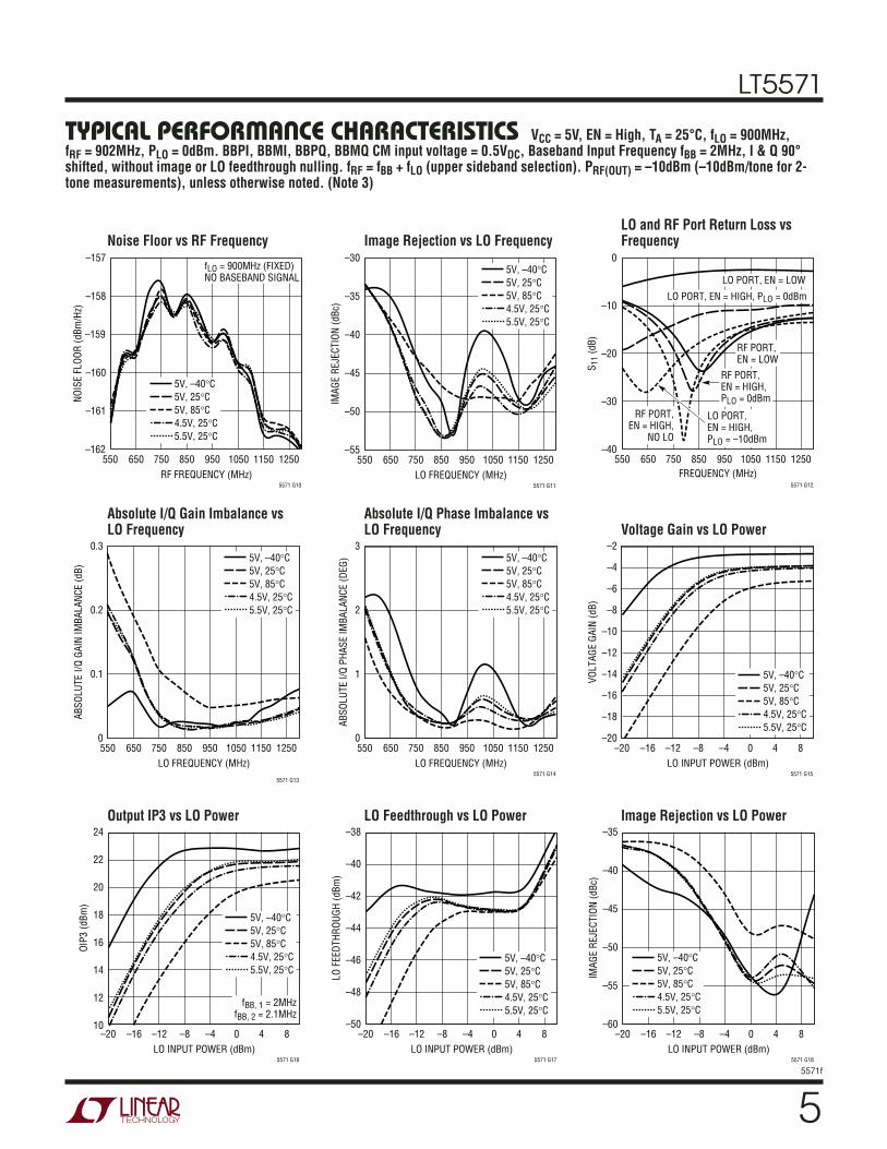
TYPICAL PERFORMANCE CHARACTERISTICS
Supply Current vs Supply Voltage
RF Output Power vs LO Frequency at 1VP-P Differential Baseband Drive Voltage Gain vs LO Frequency
Output IP3 vs LO Frequency Output IP2 vs LO FrequencyOutput 1dB Compression vs LO Frequency
LO Feedthrough to RF Output vs LO Frequency
2 • LO Leakage to RF Output vs 2 • LO Frequency
3 • LO Leakage to RF Output vs 3 • LO Frequency
VCC = 5V, EN = High, TA = 25°C, fLO = 900MHz, fRF = 902MHz, PLO = 0dBm. BBPI, BBMI, BBPQ, BBMQ CM input voltage = 0.5VDC, Baseband Input Frequency fBB = 2MHz, I & Q 90° shifted, without image or LO feedthrough nulling. fRF = fBB + fLO (upper sideband selection). PRF(OUT) = –10dBm (–10dBm/tone for 2-tone measurements), unless otherwise noted. (Note 3)
LT5571
55571f
RF FREQUENCY (MHz)550 1150 1250
5571 G10
650 750 850 1050950
5V, –40°C5V, 25°C5V, 85°C4.5V, 25°C5.5V, 25°C
–162
–160
–157
–161
–158
–159
NOIS
E FL
OOR
(dBm
/Hz)
fLO = 900MHz (FIXED)NO BASEBAND SIGNAL
LO FREQUENCY (MHz)550
IMAG
E RE
JECT
ION
(dBc
)
–35
–30
1150 1250
5571 G11
–40
–45
650 750 850 1050950
–50
–55
5V, –40°C5V, 25°C5V, 85°C4.5V, 25°C5.5V, 25°C
FREQUENCY (MHz)
–40
S 11
(dB)
–30
0
5571 G12
–10
–20
550 1150 1250650 750 850 1050950
LO PORT, EN = LOW
RF PORT,EN = HIGH,
NO LO
RF PORT,EN = LOW
LO PORT, EN = HIGH, PLO = 0dBm
LO PORT,EN = HIGH,PLO = –10dBm
RF PORT,EN = HIGH,PLO = 0dBm
LO FREQUENCY (MHz)550
ABSO
LUTE
I/Q
GAIN
IMBA
LANC
E (d
B)
0.3
0.2
1150 1250
5571 G13
0.1
650 750 850 10509500
5V, –40°C5V, 25°C5V, 85°C4.5V, 25°C5.5V, 25°C
LO FREQUENCY (MHz)550
ABSO
LUTE
I/Q
PHAS
E IM
BALA
NCE
(DEG
)
3
1150 1250
5571 G14
2
1
650 750 850 10509500
5V, –40°C5V, 25°C5V, 85°C4.5V, 25°C5.5V, 25°C
LO INPUT POWER (dBm)–20
VOLT
AGE
GAIN
(dB)
–2
4 8
5571 G15
–6
–8
–10
–12
–14
–4
–16
–18
–16 –12 –8 0–4–20
5V, –40°C5V, 25°C5V, 85°C4.5V, 25°C5.5V, 25°C
LO INPUT POWER (dBm)–20
OIP3
(dBm
)
24
4 8
5571 G16
20
18
16
14
12
22
10–16 –12 –8 0–4
fBB, 1 = 2MHzfBB, 2 = 2.1MHz
5V, –40°C5V, 25°C5V, 85°C4.5V, 25°C5.5V, 25°C
LO INPUT POWER (dBm)–20
IMAG
E RE
JECT
ION
(dBc
)
–35
4 8
5571 G18
–40
–45
–50
–60
–55
–16 –12 –8 0–4
5V, –40°C5V, 25°C5V, 85°C4.5V, 25°C5.5V, 25°C
TYPICAL PERFORMANCE CHARACTERISTICS
Noise Floor vs RF Frequency Image Rejection vs LO FrequencyLO and RF Port Return Loss vs Frequency
Absolute I/Q Gain Imbalance vs LO Frequency
Absolute I/Q Phase Imbalance vs LO Frequency Voltage Gain vs LO Power
Output IP3 vs LO Power LO Feedthrough vs LO Power Image Rejection vs LO Power
VCC = 5V, EN = High, TA = 25°C, fLO = 900MHz, fRF = 902MHz, PLO = 0dBm. BBPI, BBMI, BBPQ, BBMQ CM input voltage = 0.5VDC, Baseband Input Frequency fBB = 2MHz, I & Q 90° shifted, without image or LO feedthrough nulling. fRF = fBB + fLO (upper sideband selection). PRF(OUT) = –10dBm (–10dBm/tone for 2-tone measurements), unless otherwise noted. (Note 3)
LO INPUT POWER (dBm)–20
LO F
EEDT
HROU
GH (d
Bm)
–38
–40
–42
4 8
5571 G17
–46
–48
–50
–44
–16 –12 –8 0–4
5V, –40°C5V, 25°C5V, 85°C4.5V, 25°C5.5V, 25°C
LT5571
65571f
GAIN (dB)–6–6.5
25
20
15
10
5
0
5571 G25
–5.5 –5 –4.5 –4 –3.5 –3 –2.5 –2
PERC
ENTA
GE (%
)
–40°C25°C85°C
VBB = 400mVP-P
NOISE FLOOR (dBm/Hz)–159.9
25
20
15
10
5
0
5571 G26
–159.6 –159.3 –159.0 –158.7
PERC
ENTA
GE (%
)
–40°C25°C85°C
LO LEAKAGE (dBm)<–50
20
10
0
5571 G27
–36–38 –34–46–48 –44 –42 –40
PERC
ENTA
GE (%
)
–40°C25°C85°C
VBB = 400mVP-P
I AND Q BASEBAND VOLTAGE (VP-P,DIFF, EACH TONE)0.1
–80
–70
P TON
E (d
Bm),
IM2,
IM3
(dBc
)
–50
–30
10
RF
IM3
IM2
1 10
5571 G23
–10
–60
–40
0
–20 IM2 = POWER AT fLO + 4.1MHzIM3 = MAX POWERAT fLO + 1.9MHz OR fLO + 2.2MHz
fBBI = 2MHz, 2.1MHz, 0°fBBQ = 2MHz, 2.1MHz, 90°
25°C85°C–40°C
I AND Q BASEBAND VOLTAGE (VP-P, DIFF)0
HD2,
HD3
(dBc
)
RF CW OUTPUT POW
ER (dBm)
0
–10
–20
4 5
5571 G19
–50
–60
–40
–70
–80
–30
20
10
0
–30
–40
–20
–50
–60
–10
1 2 3
HD3
RF
HD2
HD2 = MAX POWER ATfLO + 2 • fBB OR fLO – 2 • fBBHD3 = MAX POWER ATfLO + 3 • fBB OR fLO – 3 • fBB
25°C85°C–40°C
I AND Q BASEBAND VOLTAGE (VP-P, DIFF)0
HD2,
HD3
(dBc
)
RF CW OUTPUT POW
ER (dBm)
–10
–20
4 5
5571 G20
–50
–60
–40
–70
–80
–30
10
0
–30
–40
–20
–50
–60
–10
1 2 3
HD3
RF
HD2
HD2 = MAX POWER ATfLO + 2 • fBB OR fLO – 2 • fBBHD3 = MAX POWER ATfLO + 3 • fBB OR fLO – 3 • fBB
5V5.5V4.5V
I AND Q BASEBAND VOLTAGE (VP-P, DIFF)0
LO F
EEDT
HROU
GH (d
Bm)
–30
4 5
5571 G21
–40
–45
–35
1 2 3
5V, –40°C5V, 25°C5V, 85°C4.5V, 25°C5.5V, 25°C
I AND Q BASEBAND VOLTAGE (VP-P,DIFF)0
IMAG
E RE
JECT
ION
(dBc
)
–48
4
5571 G22
–50
–52
–54
–56
–581 2 3 5
–465V, –40°C5V, 25°C5V, 85°C4.5V, 25°C5.5V, 25°C
I AND Q BASEBAND VOLTAGE (VP-P,DIFF, EACH TONE)0.1
–80
–70
P TON
E (d
Bm),
IM2,
IM3
(dBc
)
–50
–30
10
RF
IM3
IM2
1 10
5571 G24
–10
–60
–40
0
–20 IM2 = POWER AT fLO + 4.1MHzIM3 = MAX POWERAT fLO + 1.9MHz OR fLO + 2.2MHz
fBBI = 2MHz, 2.1MHz, 0°fBBQ = 2MHz, 2.1MHz, 90°
5V5.5V4.5V
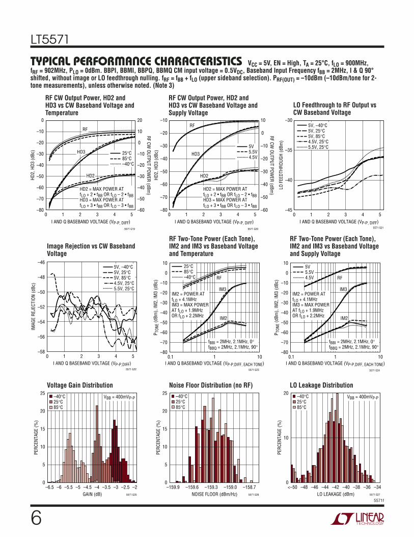
TYPICAL PERFORMANCE CHARACTERISTICS
RF CW Output Power, HD2 and HD3 vs CW Baseband Voltage and Temperature
RF CW Output Power, HD2 and HD3 vs CW Baseband Voltage and Supply Voltage
LO Feedthrough to RF Output vs CW Baseband Voltage
Image Rejection vs CW Baseband Voltage
RF Two-Tone Power (Each Tone), IM2 and IM3 vs Baseband Voltage and Temperature
RF Two-Tone Power (Each Tone), IM2 and IM3 vs Baseband Voltage and Supply Voltage
Voltage Gain Distribution Noise Floor Distribution (no RF) LO Leakage Distribution
VCC = 5V, EN = High, TA = 25°C, fLO = 900MHz, fRF = 902MHz, PLO = 0dBm. BBPI, BBMI, BBPQ, BBMQ CM input voltage = 0.5VDC, Baseband Input Frequency fBB = 2MHz, I & Q 90° shifted, without image or LO feedthrough nulling. fRF = fBB + fLO (upper sideband selection). PRF(OUT) = –10dBm (–10dBm/tone for 2-tone measurements), unless otherwise noted. (Note 3)
LT5571
75571f
TEMPERATURE (°C)
–90
LO F
EEDT
HROU
GH (d
Bm),
IR (d
B)
–70
–80
–40
5571 G29
–50
–60
–40 60 80–20 0 4020
LO FEEDTHROUGH
IMAGE REJECTION
CALIBRATED WITH PRF = 0dBmfBBI = 2MHz, 0°fBBQ = 2MHz, 90° + ϕCAL
IMAGE REJECTION (dBc)
25
20
15
10
5
0
5571 G28
PERC
ENTA
GE (%
)
–40°C25°C85°C
<–60 –56 –52 –36–48 –44 –40
VBB = 400mVP-P
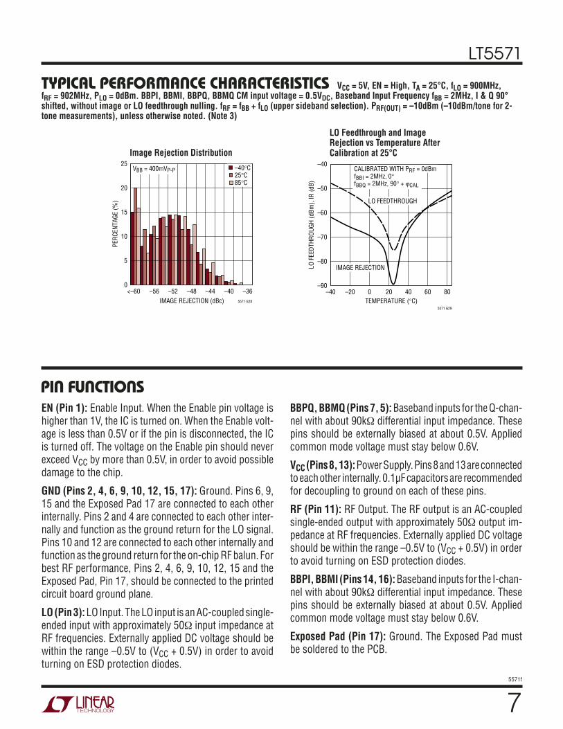
TYPICAL PERFORMANCE CHARACTERISTICS
Image Rejection Distribution
LO Feedthrough and Image Rejection vs Temperature After Calibration at 25°C
VCC = 5V, EN = High, TA = 25°C, fLO = 900MHz, fRF = 902MHz, PLO = 0dBm. BBPI, BBMI, BBPQ, BBMQ CM input voltage = 0.5VDC, Baseband Input Frequency fBB = 2MHz, I & Q 90° shifted, without image or LO feedthrough nulling. fRF = fBB + fLO (upper sideband selection). PRF(OUT) = –10dBm (–10dBm/tone for 2-tone measurements), unless otherwise noted. (Note 3)
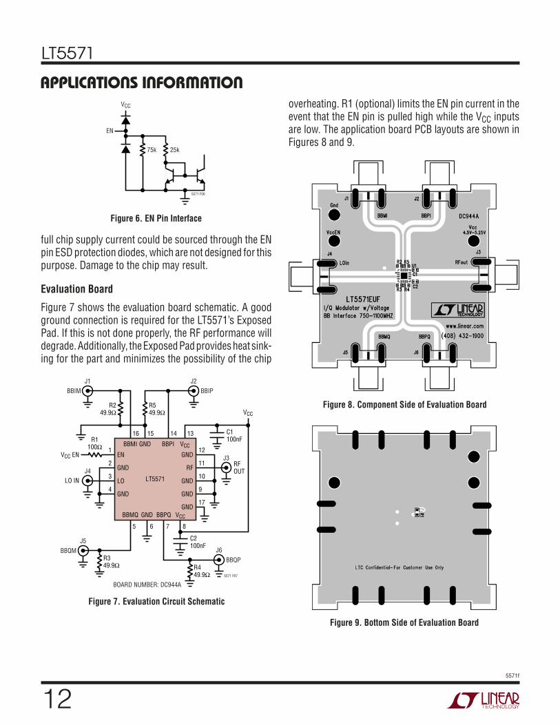
PIN FUNCTIONSEN (Pin 1): Enable Input. When the Enable pin voltage is higher than 1V, the IC is turned on. When the Enable volt-age is less than 0.5V or if the pin is disconnected, the IC is turned off. The voltage on the Enable pin should never exceed VCC by more than 0.5V, in order to avoid possible damage to the chip.
GND (Pins 2, 4, 6, 9, 10, 12, 15, 17): Ground. Pins 6, 9, 15 and the Exposed Pad 17 are connected to each other internally. Pins 2 and 4 are connected to each other inter-nally and function as the ground return for the LO signal. Pins 10 and 12 are connected to each other internally and function as the ground return for the on-chip RF balun. For best RF performance, Pins 2, 4, 6, 9, 10, 12, 15 and the Exposed Pad, Pin 17, should be connected to the printed circuit board ground plane.
LO (Pin 3): LO Input. The LO input is an AC-coupled single-ended input with approximately 50Ω input impedance at RF frequencies. Externally applied DC voltage should be within the range –0.5V to (VCC + 0.5V) in order to avoid turning on ESD protection diodes.
BBPQ, BBMQ (Pins 7, 5): Baseband inputs for the Q-chan-nel with about 90kΩ differential input impedance. These pins should be externally biased at about 0.5V. Applied common mode voltage must stay below 0.6V.
VCC (Pins 8, 13): Power Supply. Pins 8 and 13 are connected to each other internally. 0.1µF capacitors are recommended for decoupling to ground on each of these pins.
RF (Pin 11): RF Output. The RF output is an AC-coupled single-ended output with approximately 50Ω output im-pedance at RF frequencies. Externally applied DC voltage should be within the range –0.5V to (VCC + 0.5V) in order to avoid turning on ESD protection diodes.
BBPI, BBMI (Pins 14, 16): Baseband inputs for the I-chan-nel with about 90kΩ differential input impedance. These pins should be externally biased at about 0.5V. Applied common mode voltage must stay below 0.6V.
Exposed Pad (Pin 17): Ground. The Exposed Pad must be soldered to the PCB.
LT5571
85571f
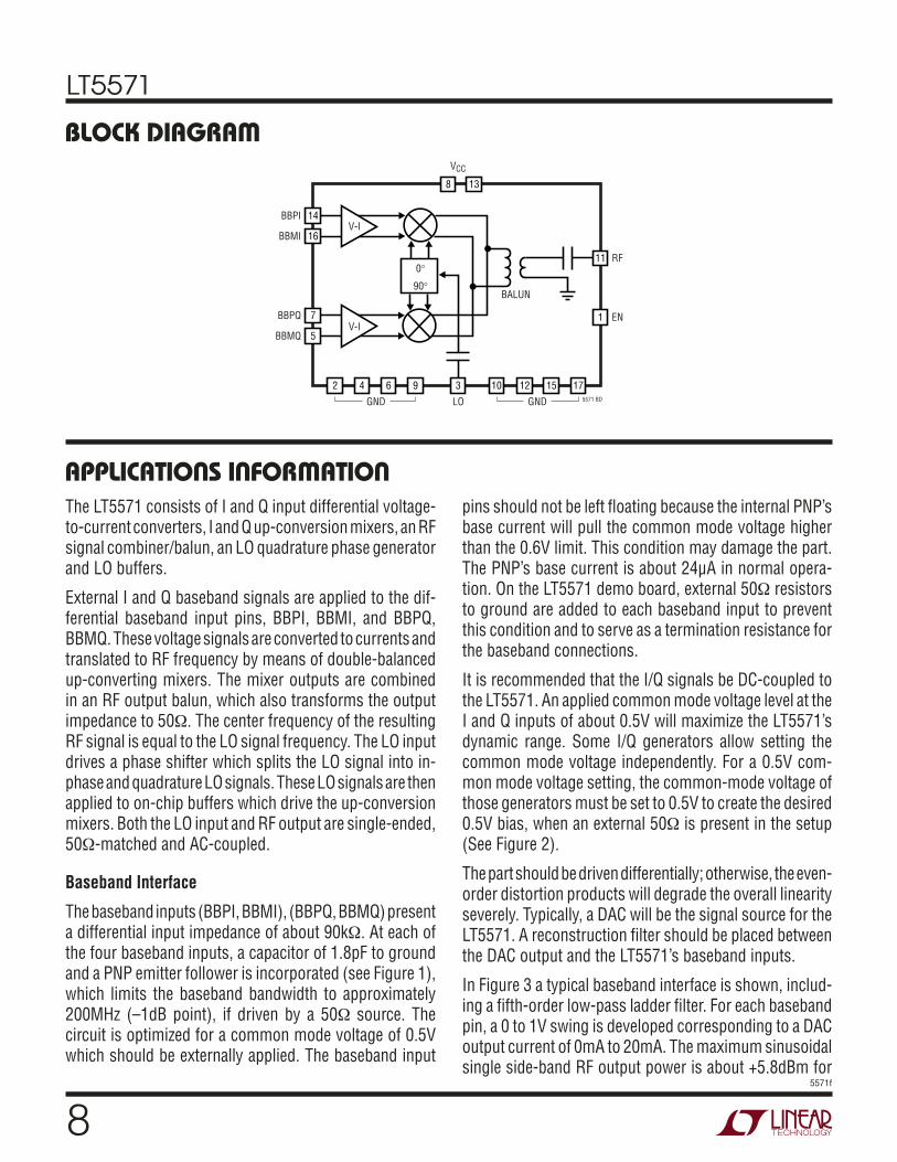
BLOCK DIAGRAM
APPLICATIONS INFORMATIONThe LT5571 consists of I and Q input differential voltage-to-current converters, I and Q up-conversion mixers, an RF signal combiner/balun, an LO quadrature phase generator and LO buffers.
External I and Q baseband signals are applied to the dif-ferential baseband input pins, BBPI, BBMI, and BBPQ, BBMQ. These voltage signals are converted to currents and translated to RF frequency by means of double-balanced up-converting mixers. The mixer outputs are combined in an RF output balun, which also transforms the output impedance to 50Ω. The center frequency of the resulting RF signal is equal to the LO signal frequency. The LO input drives a phase shifter which splits the LO signal into in-phase and quadrature LO signals. These LO signals are then applied to on-chip buffers which drive the up-conversion mixers. Both the LO input and RF output are single-ended, 50Ω-matched and AC-coupled.
Baseband Interface
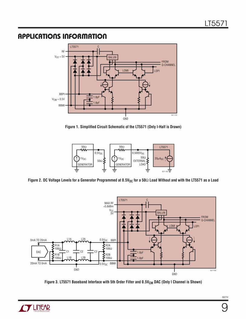
The baseband inputs (BBPI, BBMI), (BBPQ, BBMQ) present a differential input impedance of about 90kΩ. At each of the four baseband inputs, a capacitor of 1.8pF to ground and a PNP emitter follower is incorporated (see Figure 1), which limits the baseband bandwidth to approximately 200MHz (–1dB point), if driven by a 50Ω source. The circuit is optimized for a common mode voltage of 0.5V which should be externally applied. The baseband input
pins should not be left fl oating because the internal PNP’s base current will pull the common mode voltage higher than the 0.6V limit. This condition may damage the part. The PNP’s base current is about 24µA in normal opera-tion. On the LT5571 demo board, external 50Ω resistors to ground are added to each baseband input to prevent this condition and to serve as a termination resistance for the baseband connections.
It is recommended that the I/Q signals be DC-coupled to the LT5571. An applied common mode voltage level at the I and Q inputs of about 0.5V will maximize the LT5571’s dynamic range. Some I/Q generators allow setting the common mode voltage independently. For a 0.5V com-mon mode voltage setting, the common-mode voltage of those generators must be set to 0.5V to create the desired 0.5V bias, when an external 50Ω is present in the setup (See Figure 2).
The part should be driven differentially; otherwise, the even-order distortion products will degrade the overall linearity severely. Typically, a DAC will be the signal source for the LT5571. A reconstruction fi lter should be placed between the DAC output and the LT5571’s baseband inputs.
In Figure 3 a typical baseband interface is shown, includ-ing a fi fth-order low-pass ladder fi lter. For each baseband pin, a 0 to 1V swing is developed corresponding to a DAC output current of 0mA to 20mA. The maximum sinusoidal single side-band RF output power is about +5.8dBm for
90°
0°
V-I
V-I
BALUN
VCC
RF
LO 5571 BD
11
EN1
396
GND
42
5
7
16
14
8 13
BBPI
BBMI
BBPQ
BBMQ
1715
GND
1210
LT5571
95571f
APPLICATIONS INFORMATION
Figure 1. Simplifi ed Circuit Schematic of the LT5571 (Only I-Half is Drawn)
Figure 2. DC Voltage Levels for a Generator Programmed at 0.5VDC for a 50Ω Load Without and with the LT5571 as a Load
Figure 3. LT5571 Baseband Interface with 5th Order Filter and 0.5VCM DAC (Only I Channel is Shown)
RF
VCC = 5V
VCM = 0.5V
BBPI
BBMI
C
GND
LOMI
LT5571
LOPI
FROMQ-CHANNEL
5571 F01
BALUN
1.8pF
1.8pF
5571 F02
+–
50Ω
50Ω1VDC
0.5VDC 0.5005VDC
GENERATOR
50Ω
1VDC 20µADC
LT5571
50ΩEXTERNAL
LOADGENERATOR
+–
MAX RF+5.8dBm
VCC5V
BBPI
R2A100Ω
L2A
L2B
GND
0.5VDC
0.5VDC
C3R2B100Ω
BBMI
C
GND
LOMI
LT5571
LOPI
FROMQ-CHANNEL
5571 F03
BALUN
1.8pF
1.8pF
R1A100Ω
R1B100Ω
L1A
L1B
C2C1DAC
0mA TO 20mA
20mA TO 0mA
LT5571
105571f
Table 1. Typical Performance Characteristics vs VCM for fLO = 900MHz, PLO = 0dBmVCM (V) ICC (mA) GV (dB) OP1dB (dBm) OIP2 (dBm) OIP3 (dBm) NFloor (dBm/Hz) LOFT (dBm) IR (dBc)
0.1 55.3 –4.5 –1.5 53.4 9.2 –163.6 –53.6 37.00.2 65.3 –3.9 2.0 51.7 11.2 –161.8 –50.3 40.4
0.25 70.3 –3.7 3.4 51.9 13.3 –161.2 –49.0 43.50.3 75.7 –3.6 4.5 52.1 15.6 –160.5 –47.7 43.90.4 86.4 –3.5 6.3 53.1 18.7 –159.6 –45.3 45.10.5 97.1 –3.6 7.9 53.0 20.6 –158.7 –43.1 45.4 0.6 108.1 –3.7 8.4 53.7 22.1 –157.9 –41.2 45.6
APPLICATIONS INFORMATION
full 0V to 1V swing on each baseband input (2VP-P,DIFF). This maximum RF output level is limited by the 0.5VPEAK maximum baseband swing possible for a 0.5VDC com-mon-mode voltage level (assuming no negative supply bias voltage is available).
It is possible to bias the LT5571 to a common mode voltage level other than 0.5V. Table 1 shows the typical performance for different common mode voltages.
LO Section
The internal LO input amplifi er performs single-ended to differential conversion of the LO input signal. Figure 4 shows the equivalent circuit schematic of the LO input.
The internal differential LO signal is split into in-phase and quadrature (90° phase shifted) signals to drive LO buffer sections. These buffers drive the double balanced I and Q mixers. The phase relationship between the LO input and the internal in-phase LO and quadrature LO signals is fi xed, and is independent of start-up conditions. The phase shifters are designed to deliver accurate quadrature signals for an LO frequency near 900MHz. For frequen-cies signifi cantly below 750MHz or above 1100MHz, the quadrature accuracy will diminish, causing the image rejection to degrade. The LO pin input impedance is about
50Ω, and the recommended LO input power window is –2dBm to 2dBm. For PLO < –2dBm input power, the gain, OIP2, OIP3, dynamic-range (in dBc/Hz) and image rejection will degrade, especially at TA = 85°C.
Harmonics present on the LO signal can degrade the image rejection, because they introduce a small excess phase shift in the internal phase splitter. For the second (at 1.8GHz) and third harmonics (at 2.7GHz) at –20dBc level, the in-troduced signal at the image frequency is about –61dBc or lower, corresponding to an excess phase shift much less than 1 degree. For the second and third harmonics at –10dBc, still the introduced signal at the image frequency is about –51dBc. Higher harmonics than the third will have less impact. The LO return loss typically will be better than 11dB over the 750MHz to 1GHz range. Table 2 shows the LO port input impedance vs frequency.
Table 2. LO Port Input Impedance vs Frequency for EN = High and PLO = 0dBm
FREQUENCY INPUT IMPEDANCE S11(MHz) (Ω) Mag Angle500 47.2 + j11.7 0.123 97600 58.4 + j8.3 0.108 40700 65.0 – j0.6 0.131 –2800 66.1 – j12.2 0.173 –31900 60.7 – j22.5 0.221 –53
1000 53.3 – j25.1 0.239 –691100 48.4 – j25.1 0.248 –791200 42.7 – j26.4 0.285 –89
The return loss S11 on the LO port can be improved at lower frequencies by adding a shunt capacitor. The input impedance of the LO port is different if the part is in shut-down mode. The LO input impedance for EN = Low is given in Table 3.Figure 4. Equivalent Circuit Schematic of the LO Input
VCC
20pFLOINPUT
ZIN ≈ 60Ω
5571 F04
LT5571
115571f
APPLICATIONS INFORMATIONTable 3. LO Port Input Impedance vs Frequency for EN = Low and PLO = 0dBm
FREQUENCY INPUT IMPEDANCE S11(MHz) (Ω) Mag Angle500 35.6 + j42.1 0.467 83600 65.5 + j70.1 0.531 46700 163 + j76.3 0.602 14800 188 – j95.2 0.654 –13900 72.9 – j114 0.692 –361000 34.3 – j83.5 0.715 –561100 21.6 – j63.3 0.726 –731200 16.4 – j50.5 0.727 –86
RF Section
After up-conversion, the RF outputs of the I and Q mixers are combined. An on-chip balun performs internal differential to single-ended output conversion, while transforming the output signal impedance to 50Ω. Table 4 shows the RF port output impedance vs frequency.
Table 4. RF Port Output Impedance vs Frequency for EN = High and PLO = 0dBm
FREQUENCY OUTPUT IMPEDANCE S22(MHz) (Ω) Mag Angle500 22.2 + j5.2 0.390 165600 28.4 + j11.7 0.311 143700 38.8 + j14.3 0.202 119800 49.4 + j6.8 0.068 91900 49.4 – j5.8 0.058 –921000 42.7 – j11.7 0.149 –1151100 36.9 – j12.6 0.207 –1281200 33.2 – j11.3 0.241 –138
The RF output S22 with no LO power applied is given in Table 5.
Table 5. RF Port Output Impedance vs Frequency for EN = High and No LO Power Applied
FREQUENCY OUTPUT IMPEDANCE S22(MHz) (Ω) Mag Angle500 22.9 + j5.3 0.377 165600 30.0 + j11.2 0.283 143700 40.6 + j11.2 0.160 123800 47.3 + j1.9 0.034 145900 44.2 – j7.4 0.099 –1231000 38.4 – j10.4 0.175 –1311100 34.2 – j10.2 0.221 –1401200 31.7 – j8.7 0.246 –148
For EN = Low the S22 is given in Table 6.
Table 6. RF Port Output Impedance vs Frequency for EN = LowFREQUENCY OUTPUT IMPEDANCE S22
(MHz) (Ω) Mag Angle500 21.5 + j5.0 0.403 166600 26.9 + j11.8 0.333 144700 36.5 + j16.0 0.239 120800 48.8 + j11.2 0.113 89900 52.8 – j2.2 0.035 –38
1000 46.6 – j11.5 0.123 –991100 39.7 – j13.9 0.191 –1171200 35.0 – j13.0 0.232 –130
To improve S22 for lower frequencies, a series capacitor can be added to the RF output. At higher frequencies, a shunt inductor can improve the S22. Figure 5 shows the equivalent circuit schematic of the RF output.
Note that an ESD diode is connected internally from the RF output to ground. For strong output RF signal levels (higher than 3dBm) this ESD diode can degrade the lin-earity performance if an external 50Ω termination imped-ance is connected directly to ground. To prevent this, a coupling capacitor can be inserted in the RF output line. This is strongly recommended during 1dB compression measurements.
21pF
VCC
1pF47Ω
RFOUTPUT
7nH
5571 F05
Figure 5. Equivalent Circuit Schematic of the RF Output
Enable Interface
Figure 6 shows a simplifi ed schematic of the EN pin inter-face. The voltage necessary to turn on the LT5571 is 1V. To disable (shut down) the chip, the enable voltage must be below 0.5V. If the EN pin is not connected, the chip is disabled. This EN = Low condition is guaranteed by the 75kΩ on-chip pull-down resistor.
It is important that the voltage at the EN pin does not exceed VCC by more than 0.5V. If this should occur, the
LT5571
125571f
APPLICATIONS INFORMATION
full chip supply current could be sourced through the EN pin ESD protection diodes, which are not designed for this purpose. Damage to the chip may result.
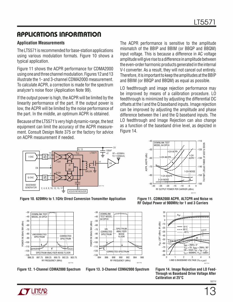
Evaluation Board
Figure 7 shows the evaluation board schematic. A good ground connection is required for the LT5571’s Exposed Pad. If this is not done properly, the RF performance will degrade. Additionally, the Exposed Pad provides heat sink-ing for the part and minimizes the possibility of the chip
EN
VCC
75k
5571 F06
25k
Figure 6. EN Pin Interface
BBIPBBIMJ1
16 15
R549.9Ω
R1100Ω
VCC EN
LO IN
R249.9Ω
14 13
VCC
9
10
11
12
4
3
2
1
5 6 7 8
5571 F07
17
R349.9Ω
C2100nF
C1100nF
RFOUT
BBQMBBQP
BOARD NUMBER: DC944A
J6
J3
J4
J5
R449.9Ω
J2
BBMI
LT5571
BBPI VCC
BBMQ GND
GND
BBPQ VCC
GND
GND
RF
GND
GND
LO
GND
EN
GND
Figure 7. Evaluation Circuit Schematic
Figure 8. Component Side of Evaluation Board
Figure 9. Bottom Side of Evaluation Board
overheating. R1 (optional) limits the EN pin current in the event that the EN pin is pulled high while the VCC inputs are low. The application board PCB layouts are shown in Figures 8 and 9.
LT5571
135571f
RF OUTPUT POWER PER CARRIER (dBm)–30
ACPR
, AltC
PR (d
Bc)
NOISE FLOOR AT 30MHz OFFSET (dBm
/Hz)
–70
–60
–10
5571 F11
–80
–90–25 –20 –15 0–5
–40
–50
–140
–130
–150
–160
–110
–120
DOWNLINK TESTMODEL 64 DPCH
3-CH ACPR
1-CHACPR3-CH AltCPR
1-CH AltCPR
3-CH NOISE
1-CH NOISE
I AND Q BASEBAND VOLTAGE (VP-P,DIFF)0
–90
–80
–70
P RF,
LOF
T (d
Bm),
IR (d
Bc)
–50
–30
20
10
IR
1 5432
5571 F14
–10
–60
–40
0
–20
fBBI = 2MHz, 0°VCC = 5V, fBBQ = 2MHz, 90°EN = HIGH, fRF = fBB + fLOfLO = 900MHz, PLO = 0dBm
25°C85°C–40°C
LO FT
PRF
APPLICATIONS INFORMATIONApplication Measurements
The LT5571 is recommended for base-station applications using various modulation formats. Figure 10 shows a typical application.
Figure 11 shows the ACPR performance for CDMA2000 using one and three channel modulation. Figures 12 and 13 illustrate the 1- and 3-channel CDMA2000 measurement. To calculate ACPR, a correction is made for the spectrum analyzer’s noise fl oor (Application Note 99).
If the output power is high, the ACPR will be limited by the linearity performance of the part. If the output power is low, the ACPR will be limited by the noise performance of the part. In the middle, an optimum ACPR is obtained.
Because of the LT5571’s very high dynamic-range, the test equipment can limit the accuracy of the ACPR measure-ment. Consult Design Note 375 or the factory for advice on ACPR measurement if needed.
VCO/SYNTHESIZER
EN
2, 4, 6, 9, 10, 12, 15, 17
I-CH
Q-CH BALUN
VCC
V-I
BASEBANDGENERATOR
V-I
LT5571
5V
14
16
1
7
5
8, 13
5571 F10
11PA
RF = 620MHzTO 1100MvHz
3
I-DAC
Q-DAC
90°
0°
100nF×2
Figure 10. 620MHz to 1.1GHz Direct Conversion Transmitter Application Figure 11. CDMA2000 ACPR, ALTCPR and Noise vs RF Output Power at 900MHz for 1 and 3 Carriers
Figure 12. 1-Channel CDMA2000 Spectrum Figure 13. 3-Channel CDMA2000 Spectrum
896.25 899.25 902.25 903.75
5571 F12
897.75 900.75
CORRECTEDSPECTRUM
DOWNLINK TESTMODEL 64 DPCH
SPECTRUM ANALYSER NOISE FLOOR
RF FREQUENCY (MHz)
–130
–120
POW
ER IN
30k
Hz B
W (d
Bm)
–110
–90
–80
–70
–30
–100
–60
–50
–40
UNCORRECTEDSPECTRUM
RF FREQUENCY (MHz)894
–130
–120
POW
ER IN
30k
Hz B
W (d
Bm)
–110
–90
–80
–70
902
–30
5571 F13
–100
898896 904900 906
–60
–50
–40
UN-CORRECTEDSPECTRUM
DOWNLINKTEST MODEL 64 DPCH
CORRECTED SPECTRUM
SPECTRUMANALYSER
NOISEFLOOR
The ACPR performance is sensitive to the amplitude mismatch of the BBIP and BBIM (or BBQP and BBQM) input voltage. This is because a difference in AC voltage amplitude will give rise to a difference in amplitude between the even-order harmonic products generated in the internal V-I converter. As a result, they will not cancel out entirely. Therefore, it is important to keep the amplitudes at the BBIP and BBIM (or BBQP and BBQM) as equal as possible.
LO feedthrough and image rejection performance may be improved by means of a calibration procedure. LO feedthrough is minimized by adjusting the differential DC offsets at the I and the Q baseband inputs. Image rejection can be improved by adjusting the amplitude and phase difference between the I and the Q baseband inputs. The LO feedthrough and Image Rejection can also change as a function of the baseband drive level, as depicted in Figure 14.
Figure 14. Image Rejection and LO Feed-Through vs Baseband Drive Voltage After Calibration at 25°C
LT5571
145571f
865.4 865.8 866.2 866.4
5571 F16a
865.6 866.0
CH BANDWIDTH: 100kHzCH SPACING: 100kHzCH PWR: –4.85dBmACP UP: –33.74dBcACP LOW: –37.76dBc
ALT1 UP: –71.15dBcALT1 LOW: –64.52dBcALT2 UP: –72.80dBcALT2 LOW: –72.42dBc
FREQUENCY (MHz)
–100
–20
POW
ER IN
3kH
z BW
(dBm
), M
ASK
(dBc
h) –10
–90
–80
–70
0
–30
–60
–50
–40
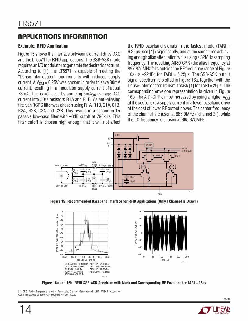
APPLICATIONS INFORMATIONExample: RFID Application
Figure 15 shows the interface between a current drive DAC and the LT5571 for RFID applications. The SSB-ASK mode requires an I/Q modulator to generate the desired spectrum. According to [1], the LT5571 is capable of meeting the “Dense-Interrogator” requirements with reduced supply current. A VCM = 0.25V was chosen in order to save 30mA current, resulting in a modulator supply current of about 73mA. This is achieved by sourcing 5mADC average DAC current into 50Ω resistors R1A and R1B. As anti-aliasing fi lter, an RCRC fi lter was chosen using R1A, R1B, C1A, C1B, R2A, R2B, C2A and C2B. This results in a second-order passive low-pass fi lter with –3dB cutoff at 790kHz. This fi lter cutoff is chosen high enough that it will not affect
the RFID baseband signals in the fastest mode (TARI = 6.25µs, see [1]) signifi cantly, and at the same time achiev-ing enough alias attenuation while using a 32MHz sampling frequency. The resulting Alt80-CPR (the alias frequency at 897.875MHz falls outside the RF frequency range of Figure 16a) is –92dBc for TARI = 6.25µs. The SSB-ASK output signal spectrum is plotted in Figure 16a, together with the Dense-Interrogator Transmit mask [1] for TARI = 25µs. The corresponding envelope representation is given in Figure 16b. The Alt1-CPR can be increased by using a higher VCM at the cost of extra supply current or a lower baseband drive at the cost of lower RF output power. The center frequency of the channel is chosen at 865.9MHz (“channel 2”), while the LO frequency is chosen at 865.875MHz.
RF
VCC5V
BBPI
GND
0.25VDC
0.25VDC
0.25VDC
0.25VDC BBMI
C
GND
LOMI
LT5571
LOPI
FROMQ-CHANNEL
5571 F15
BALUN
1.8pF
1.8pF
R1A50Ω
R2A250Ω
R1B50Ω
C2A470pF
C1A2.2nF
C2B470pF
C1B2.2nF
DAC
0mA TO 10mA
10mA TO 0mA R2B250Ω
Figure 15. Recommended Baseband Interface for RFID Applications (Only I Channel is Drawn)
Figure 16a and 16b. RFID SSB-ASK Spectrum with Mask and Corresponding RF Envelope for TARI = 25µs
0 100 200 250
5571 F16b
50 150TIME (µs)
–0.3
RF O
UTPU
T VO
LTAG
E (V
)
–0.2
–0.1
0.3
0
0.1
0.2
[1] EPC Radio Frequency Identity Protocols, Class-1 Generation-2 UHF RFID Protocol for Communications at 860MHz – 960MHz, version 1.0.9.
LT5571
155571f
Information furnished by Linear Technology Corporation is believed to be accurate and reliable. However, no responsibility is assumed for its use. Linear Technology Corporation makes no representa-tion that the interconnection of its circuits as described herein will not infringe on existing patent rights.
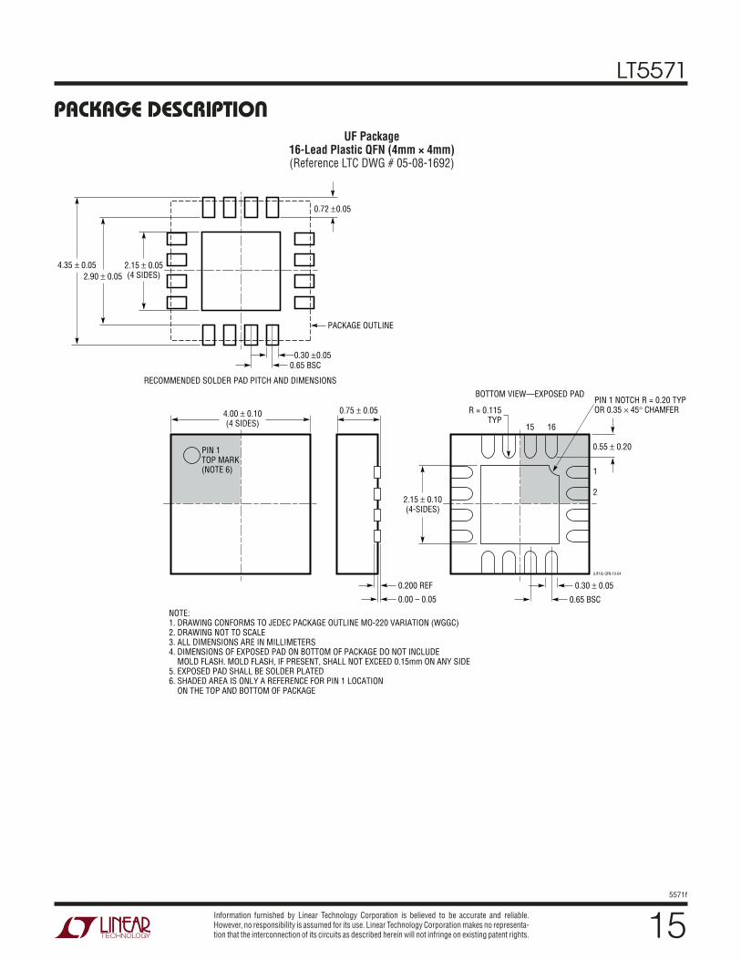
PACKAGE DESCRIPTION
4.00 ± 0.10(4 SIDES)
NOTE:1. DRAWING CONFORMS TO JEDEC PACKAGE OUTLINE MO-220 VARIATION (WGGC)2. DRAWING NOT TO SCALE3. ALL DIMENSIONS ARE IN MILLIMETERS4. DIMENSIONS OF EXPOSED PAD ON BOTTOM OF PACKAGE DO NOT INCLUDE MOLD FLASH. MOLD FLASH, IF PRESENT, SHALL NOT EXCEED 0.15mm ON ANY SIDE5. EXPOSED PAD SHALL BE SOLDER PLATED6. SHADED AREA IS ONLY A REFERENCE FOR PIN 1 LOCATION ON THE TOP AND BOTTOM OF PACKAGE
PIN 1TOP MARK(NOTE 6)
0.55 ± 0.20
1615
1
2
BOTTOM VIEW—EXPOSED PAD
2.15 ± 0.10(4-SIDES)
0.75 ± 0.05 R = 0.115TYP
0.30 ± 0.05
0.65 BSC
0.200 REF
0.00 – 0.05
(UF16) QFN 10-04
RECOMMENDED SOLDER PAD PITCH AND DIMENSIONS
0.72 ±0.05
0.30 ±0.050.65 BSC
2.15 ± 0.05(4 SIDES)2.90 ± 0.05
4.35 ± 0.05
PACKAGE OUTLINE
PIN 1 NOTCH R = 0.20 TYPOR 0.35 × 45° CHAMFER
UF Package16-Lead Plastic QFN (4mm × 4mm)(Reference LTC DWG # 05-08-1692)
LT5571
165571f
Linear Technology Corporation1630 McCarthy Blvd., Milpitas, CA 95035-7417 (408) 432-1900 FAX: (408) 434-0507 www.linear.com © LINEAR TECHNOLOGY CORPORATION 2006
LT 1206 PRINTED IN USA
PART NUMBER DESCRIPTION COMMENTSInfrastructureLT5514 Ultralow Distortion, IF Amplifi er/ADC Driver
with Digitally Controlled Gain850MHz Bandwidth, 47dBm OIP3 at 100MHz, 10.5dB to 33dB Gain Control Range
LT5515 1.5GHz to 2.5GHz Direct Conversion Quadrature Demodulator
20dBm IIP3, Integrated LO Quadrature Generator
LT5516 0.8GHz to 1.5GHz Direct Conversion Quadrature Demodulator
21.5dBm IIP3, Integrated LO Quadrature Generator
LT5517 40MHz to 900MHz Quadrature Demodulator 21dBm IIP3, Integrated LO Quadrature GeneratorLT5518 1.5GHz to 2.4GHz High Linearity Direct
Quadrature Modulator22.8dBm OIP3 at 2GHz, –158.2dBm/Hz Noise Floor, 50Ω Single-Ended RF and LO Ports, 4-Channel W-CDMA ACPR = –64dBc at 2.14GHz
LT5519 0.7GHz to 1.4GHz High Linearity Upconverting Mixer
17.1dBm IIP3 at 1GHz, Integrated RF Output Transformer with 50Ω Matching, Single-Ended LO and RF Ports Operation
LT5520 1.3GHz to 2.3GHz High Linearity Upconverting Mixer
15.9dBm IIP3 at 1.9GHz, Integrated RF Output Transformer with 50Ω Matching, Single-Ended LO and RF Ports Operation
LT5521 10MHz to 3700MHz High Linearity Upconverting Mixer
24.2dBm IIP3 at 1.95GHz, NF = 12.5dB, 3.15V to 5.25V Supply, Single-Ended LO Port Operation
LT5522 600MHz to 2.7GHz High Signal Level Downconverting Mixer
4.5V to 5.25V Supply, 25dBm IIP3 at 900MHz, NF = 12.5dB, 50Ω Single-Ended RF and LO Ports
LT5524 Low Power, Low Distortion ADC Driver with Digitally Programmable Gain
450MHz Bandwidth, 40dBm OIP3, 4.5dB to 27dB Gain Control
LT5525 High Linearity, Low Power Downconverting Mixer
Single-Ended 50Ω RF and LO Ports, 17.6dBm IIP3 at 1900MHz, ICC = 28mA
LT5526 High Linearity, Low Power Downconverting Mixer
3V to 5.3V Supply, 16.5dBm IIP3, 100kHz to 2GHz RF, NF = 11dB, ICC = 28mA, –65dBm LO-RF Leakage
LT5527 400MHz to 3.7GHz High Signal Level Downconverting Mixer
IIP3 = 23.5dBm and NF = 12.5dBm at 1900MHz, 4.5V to 5.25V Supply, ICC = 78mA, Conversion Gain = 2dB.
LT5528 1.5GHz to 2.4GHz High Linearity Direct Quadrature Modulator
21.8dBm OIP3 at 2GHz, –159.3dBm/Hz Noise Floor, 50Ω, 0.5VDC Baseband Interface, 4-Channel W-CDMA ACPR = –66dBc at 2.14GHz
LT5558 600MHz to 1100MHz High Linearity Direct Quadrature Modulator
22.4dBm OIP3 at 900MHz, –158dBm/Hz Noise Floor, 3kΩ, 2.1VDC Baseband Interface, 3-Ch CDMA2000 ACPR = –70.4dBc at 900MHz
LT5560 Ultra-Low Power Active Mixer 10mA Supply Current, 10dBm IIP3, 10dB NF, Usable as Up- or Down-Converter.LT5568 700MHz to 1050MHz High Linearity Direct
Quadrature Modulator22.9dBm OIP3 at 850MHz, –160.3dBm/Hz Noise Floor, 50Ω, 0.5VDC Baseband Interface, 3-Ch CDMA2000 ACPR = –71.4dBc at 850MHz
LT5572 1.5GHz to 2.5GHz High Linearity Direct Quadrature Modulator
21.6dBm OIP3 at 2GHz, –158.6dBm/Hz Noise Floor, High-Ohmic 0.5VDC Baseband Interface, 4-Ch W-CDMA ACPR = –67.7dBc at 2.14GHz
RF Power DetectorsLTC®5505 RF Power Detectors with >40dB Dynamic Range 300MHz to 3GHz, Temperature Compensated, 2.7V to 6V SupplyLTC5507 100kHz to 1000MHz RF Power Detector 100kHz to 1GHz, Temperature Compensated, 2.7V to 6V SupplyLTC5508 300MHz to 7GHz RF Power Detector 44dB Dynamic Range, Temperature Compensated, SC70 PackageLTC5509 300MHz to 3GHz RF Power Detector 36dB Dynamic Range, Low Power Consumption, SC70 PackageLTC5530 300MHz to 7GHz Precision RF Power Detector Precision VOUT Offset Control, Shutdown, Adjustable GainLTC5531 300MHz to 7GHz Precision RF Power Detector Precision VOUT Offset Control, Shutdown, Adjustable OffsetLTC5532 300MHz to 7GHz Precision RF Power Detector Precision VOUT Offset Control, Adjustable Gain and OffsetLT5534 50MHz to 3GHz Log RF Power Detector with
60dB Dynamic Range±1dB Output Variation over Temperature, 38ns Response Time, Log Linear Response
LTC5536 Precision 600MHz to 7GHz RF Power Detector with Fast Comparator Output
25ns Response Time, Comparator Reference Input, Latch Enable Input, –26dBm to +12dBm Input Range
LT5537 Wide Dynamic Range Log RF/IF Detector Low Frequency to 1GHz, 83dB Log Linear Dynamic Range
RELATED PARTS
Related Documents