LPC2141/42/44/46/48 General description The LPC2141/42/44/46/48 microcontrollers are based on a 16-bit/32-bit ARM7TDMI-S CPU with real-time emulation and embedded trace support, that combine microcontroller with embedded high speed flash memory ranging from 32 kB to 512 kB. A 128-bit wide memory interface and a unique accelerator architecture enable 32-bit code execution at the maximum clock rate. For critical code size applications, the alternative 16-bit Thumb mode reduces code by more than 30 % with minimal performance penalty. Due to their tiny size and low power consumption, LPC2141/42/44/46/48 are ideal for applications where miniaturization is a key requirement, such as access control and point-of-sale. Serial communications interfaces ranging from a USB 2.0 Full-speed device, multiple UARTs, SPI, SSP to I2C-bus and on-chip SRAM of 8 kB up to 40 kB, make these devices very well suited for communication gateways and protocol converters, soft modems, voice recognition and low end imaging, providing both large buffer size and high processing power. Various 32-bit timers, single or dual 10-bit ADC(s), 10-bit DAC, PWM channels and 45 fast GPIO lines with up to nine edge or level sensitive external interrupt pins make these microcontrollers suitable for industrial control and medical systems. Features 16-bit/32-bit ARM7TDMI-S microcontroller in a tiny LQFP64 package.

Welcome message from author
This document is posted to help you gain knowledge. Please leave a comment to let me know what you think about it! Share it to your friends and learn new things together.
Transcript
LPC2141/42/44/46/48
General description
The LPC2141/42/44/46/48 microcontrollers are based on a 16-bit/32-bit ARM7TDMI-S CPU with real-
time emulation and embedded trace support, that combine microcontroller with embedded high speed
flash memory ranging from 32 kB to 512 kB. A 128-bit wide memory interface and a unique accelerator
architecture enable 32-bit code execution at the maximum clock rate. For critical code size applications,
the alternative 16-bit Thumb mode reduces code by more than 30 % with minimal performance penalty.
Due to their tiny size and low power consumption, LPC2141/42/44/46/48 are ideal for applications
where miniaturization is a key requirement, such as access control and point-of-sale. Serial
communications interfaces ranging from a USB 2.0 Full-speed device, multiple UARTs, SPI, SSP to
I2C-bus and on-chip SRAM of 8 kB up to 40 kB, make these devices very well suited for
communication gateways and protocol converters, soft modems, voice recognition and low end imaging,
providing both large buffer size and high processing power. Various 32-bit timers, single or dual 10-bit
ADC(s), 10-bit DAC, PWM channels and 45 fast GPIO lines with up to nine edge or level sensitive
external interrupt pins make these microcontrollers suitable for industrial control and medical systems.
Features
16-bit/32-bit ARM7TDMI-S microcontroller in a tiny LQFP64 package.
8 kB to 40 kB of on-chip static RAM and 32 kB to 512 kB of on-chip flash memory. 128-
bit wide interface/accelerator enables high-speed 60 MHz operation.
In-System Programming/In-Application Programming (ISP/IAP) via on-chip boot loader
software. Single flash sector or full chip erase in 400 ms and programming of 256 bytes in 1 ms.
EmbeddedICE RT and Embedded Trace interfaces offer real-time debugging with the on-
chip RealMonitor software and high-speed tracing of instruction execution.
USB 2.0 Full-speed compliant device controller with 2 kB of endpoint RAM. In addition,
the LPC2146/48 provides 8 kB of on-chip RAM accessible to USB by DMA.
One or two (LPC2141/42 vs. LPC2144/46/48) 10-bit ADCs provide a total of 6/14 analog
inputs, with conversion times as low as 2.44 μs per channel.
Single 10-bit DAC provides variable analog output (LPC2142/44/46/48 only).
Two 32-bit timers/external event counters (with four capture and four compare channels
each), PWM unit (six outputs) and watchdog.

Low power Real-Time Clock (RTC) with independent power and 32 kHz clock input.
Single-chip 16-bit/32-bit microcontrollers
Multiple serial interfaces including two UARTs (16C550), two Fast I2C-bus (400 kbit/s),
SPI and SSP with buffering and variable data length capabilities.
Vectored Interrupt Controller (VIC) with configurable priorities and vector addresses.
Up to 45 of 5 V tolerant fast general purpose I/O pins in a tiny LQFP64 package.
Up to 21 external interrupt pins available.
60 MHz maximum CPU clock available from programmable on-chip PLL with settling
time of 100 μs.
On-chip integrated oscillator operates with an external crystal from 1 MHz to 25 MHz.
Power saving modes include Idle and Power-down.
Individual enable/disable of peripheral functions as well as peripheral clock scaling for
additional power optimization.
Processor wake-up from Power-down mode via external interrupt or BOD.
Single power supply chip with POR and BOD circuits:
CPU operating
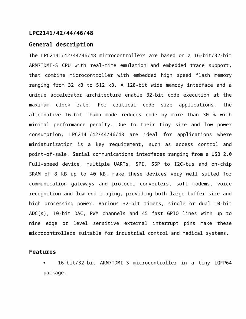
Block diagram

Pinning information

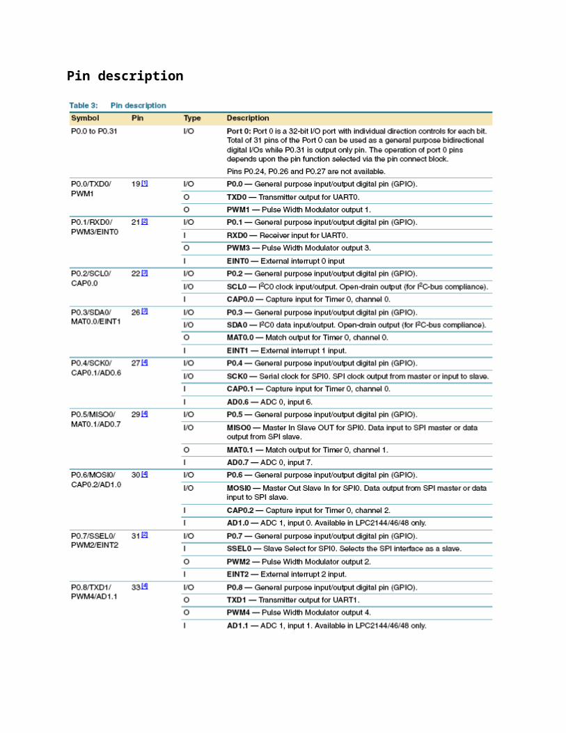
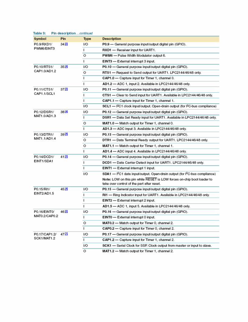
Pin description

[1] 5 V tolerant pad providing digital I/O functions with TTL levels and hysteresis and 10 ns slew rate
control.
[2] 5 V tolerant pad providing digital I/O functions with TTL levels and hysteresis and 10 ns slew rate
control. If configured for an input function, this pad utilizes built-in glitch filter that blocks pulses
shorter than 3 ns.
[3] Open-drain 5 V tolerant digital I/O I2C-bus 400 kHz specification compatible pad. It requires
external pull-up to provide an output functionality.
[4] 5 V tolerant pad providing digital I/O (with TTL levels and hysteresis and 10 ns slew rate control)
and analog input function. If configured for an input function, this pad utilizes built-in glitch filter that
blocks pulses shorter than 3 ns. When configured as an ADC input, digital section of the pad is disabled.
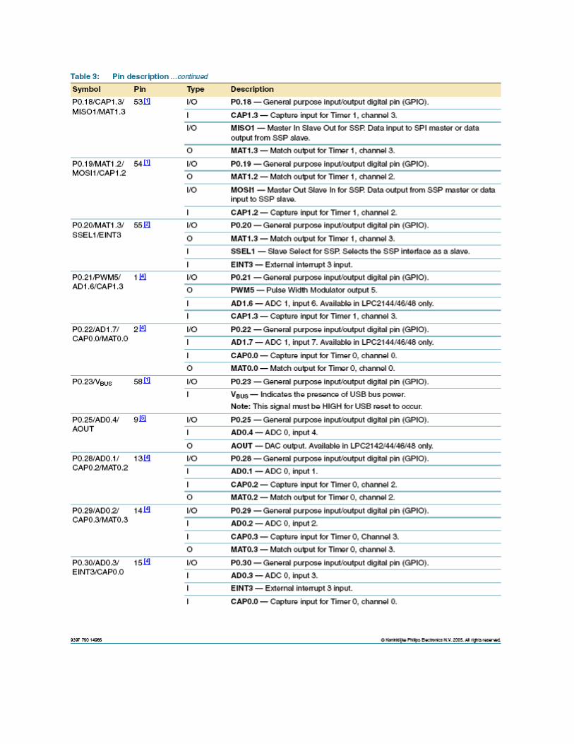
[5] 5 V tolerant pad providing digital I/O (with TTL levels and hysteresis and 10 ns slew rate control)
and analog output function. When configured as the DAC output, digital section of the pad is disabled.
[6] 5 V tolerant pad with built-in pull-up resistor providing digital I/O functions with TTL levels and
hysteresis and 10 ns slew rate control. The pull-up resistor’s value typically ranges from 60 kΩ to 300
kΩ.
[7] Pad is designed in accordance with the Universal Serial Bus (USB) specification, revision 2.0 (Full-
speed and Low-speed mode only).
[8] 5 V tolerant pad providing digital input (with TTL levels and hysteresis) function only.
[9] Pad provides special analog functionality.
1. Functional description
Architectural overview
The ARM7TDMI-S is a general purpose 32-bit microprocessor, which offers high performance and very
low power consumption. The ARM architecture is based on Reduced Instruction Set Computer (RISC)
principles, and the instruction set and related decode mechanism are much simpler than those of
microprogrammed Complex Instruction Set Computers (CISC). This simplicity results in a high
instruction throughput and impressive real-time interrupt response from a small and cost-effective
processor core. Pipeline techniques are employed so that all parts of the processing and memory systems
can operate continuously. Typically, while one instruction is being executed, its successor is being
decoded, and a third instruction is being fetched from memory. The ARM7TDMI-S processor also
employs a unique architectural strategy known as Thumb, which makes it ideally suited to high-volume
applications with memory restrictions, or applications where code density is an issue. The key idea
behind Thumb is that of a super-reduced instruction set. Essentially, the
ARM7TDMI-S processor has two instruction sets:
• The standard 32-bit ARM set.
• A 16-bit Thumb set.
The Thumb set’s 16-bit instruction length allows it to approach twice the density of standard ARM code
while retaining most of the ARM’s performance advantage over a traditional 16-bit processor using 16-
bit registers. This is possible because Thumb code operates on the same 32-bit register set as ARM code.

Thumb code is able to provide up to 65 % of the code size of ARM, and 160 % of the performance of an
equivalent ARM processor connected to a 16-bit memory system. The particular flash implementation in
the LPC2141/42/44/46/48 allows for full speed execution also in ARM mode. It is recommended to
program performance critical and short code sections (such as interrupt service routines and DSP
algorithms) in ARM mode. The impact on the overall code size will be minimal but the speed can be
increased by 30% over Thumb mode.
2. On-chip flash program memory
The LPC2148 incorporates a 32 kB, 64 kB, 128 kB, 256 kB and 512 kB flash memory system
respectively. This memory may be used for both code and data storage. Programming of the flash
memory may be accomplished in several ways. It may be programmed In System via the serial port. The
application program may also erase and/or program the flash while the application is running, allowing a
great degree of flexibility for data storage field firmware upgrades, etc. Due to the architectural solution
chosen for an on-chip boot loader, flash memory available for user’s code on LPC2141/42/44/46/48 is
32 kB, 64 kB, 128 kB, 256 kB and 500 kB respectively.
The LPC2141/42/44/46/48 flash memory provides a minimum of 100,000 erase/write cycles and 20
years of data-retention.
3. On-chip static RAM
On-chip static RAM may be used for code and/or data storage. The SRAM may be accessed as
8-bit, 16-bit, and 32-bit. The LPC2141, LPC2142/44 and LPC2146/48 provide 8 kB, 16 kB and 32 kB of
static RAM respectively. In case of LPC2146/48 only, an 8 kB SRAM block intended to be utilized
mainly by the USB can also be used as a general purpose RAM for data storage and code storage and
execution.
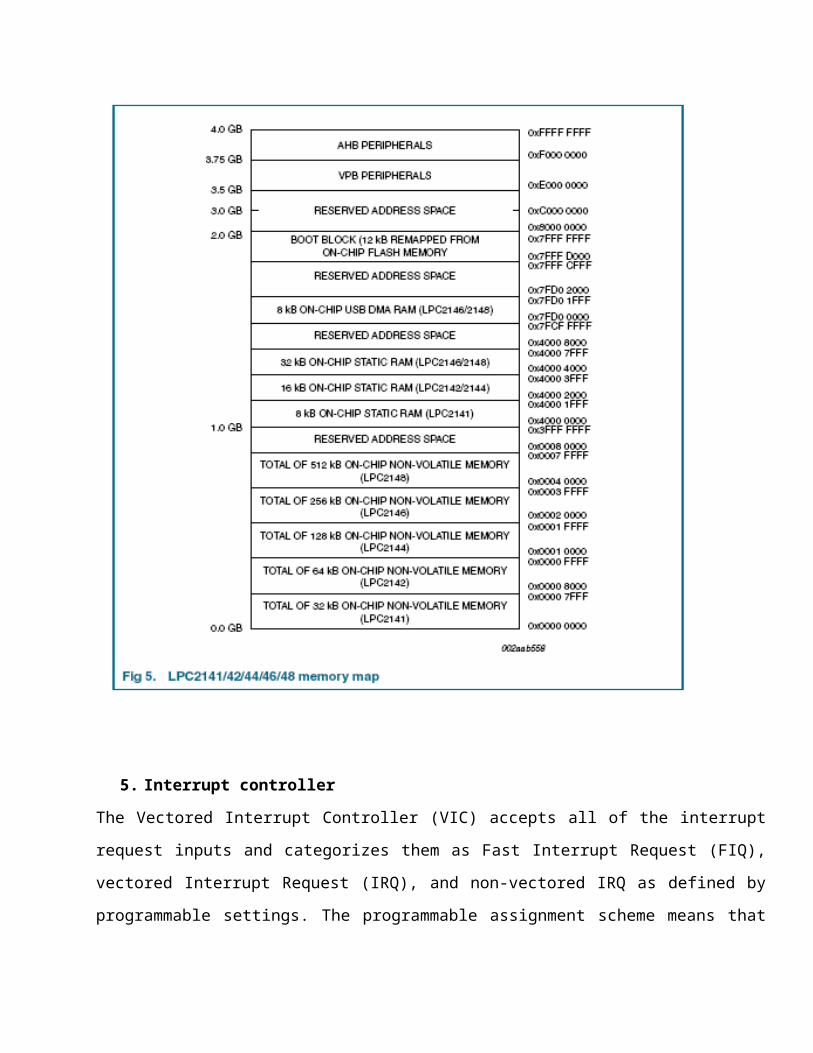
4. Memory map
The LPC2141/42/44/46/48 memory map incorporates several distinct regions, as shown in Figure 5. In
addition, the CPU interrupt vectors may be remapped to allow them to reside in either flash memory (the
default) or on-chip static RAM. This is described in “System control”.
5. Interrupt controller
The Vectored Interrupt Controller (VIC) accepts all of the interrupt request inputs and categorizes them
as Fast Interrupt Request (FIQ), vectored Interrupt Request (IRQ), and non-vectored IRQ as defined by
programmable settings. The programmable assignment scheme means that priorities of interrupts from
the various peripherals can be dynamically assigned and adjusted. Fast interrupt request (FIQ) has the
highest priority. If more than one request is assigned to FIQ, the VIC combines the requests to produce
the FIQ signal to the ARM processor. The fastest possible FIQ latency is achieved when only one
request is classified as FIQ, because then the FIQ service routine does not need to branch into the
interrupt service routine but can run from the interrupt vector location. If more than one request is
assigned to the FIQ class, the FIQ service routine will read a word from the VIC that identifies which
FIQ source(s) is (are) requesting an interrupt. Vectored IRQs have the middle priority. Sixteen of the
interrupt requests can be assigned to this category. Any of the interrupt requests can be assigned to any
of the 16 vectored IRQ slots, among which slot 0 has the highest priority and slot 15 has the lowest.
Non-vectored IRQs have the lowest priority. The VIC combines the requests from all the vectored and
non-vectored IRQs to produce the IRQ signal to the ARM processor. The IRQ service routine can start
by reading a register from the VIC and jumping there. If any of the vectored IRQs are pending, the VIC
provides the address of the highest-priority requesting IRQs service routine, otherwise it provides the
address of a default routine that is shared by all the non-vectored IRQs. The default routine can read
another VIC register to see what IRQs are active.
Interrupt sources
Each peripheral device has one interrupt line connected to the Vectored Interrupt Controller, but may
have several internal interrupt flags. Individual interrupt flags may also represent more than one
interrupt source.
6. Pin connect block
The pin connect block allows selected pins of the microcontroller to have more than one function.
Configuration registers control the multiplexers to allow connection between the pin and the on chip
peripherals. Peripherals should be connected to the appropriate pins prior to being activated, and prior to
any related interrupt(s) being enabled. Activity of any enabled peripheral function that is not mapped to
a related pin should be considered undefined. The Pin Control Module with its pin select registers
defines the functionality of the microcontroller in a given hardware environment. After reset all pins of
Port 0 and 1 are configured as input with the following exceptions: If debug is enabled, the JTAG pins
will assume their JTAG functionality; if trace is enabled, the Trace pins will assume their trace
functionality. The pins associated with the I2C0 and I2C1 interface are open drain.
7. Fast general purpose parallel I/O (GPIO)
Device pins that are not connected to a specific peripheral function are controlled by the GPIO
registers. Pins may be dynamically configured as inputs or outputs. Separate registers allow setting or
clearing any number of outputs simultaneously. The value of the output register may be read back, as
well as the current state of the port pins.
LPC214148 introduces accelerated GPIO functions over prior LPC2000 devices:
• GPIO registers are relocated to the ARM local bus for the fastest possible I/O timing.
• Mask registers allow treating sets of port bits as a group, leaving other bits unchanged.
• All GPIO registers are byte addressable.
• Entire port value can be written in one instruction.
Features
• Bit-level set and clear registers allow a single instruction set or clear of any number of bits in one port.
• Direction control of individual bits.
• Separate control of output set and clear.
• All I/O default to inputs after reset.
8. 10-bit ADC
The LPC2141/42 contain one and the LPC2144/46/48 contain two analog to digital converters. These
converters are single 10-bit successive approximation analog to digital converters. While ADC0 has six
channels, ADC1 has eight channels. Therefore, total number of available ADC inputs for LPC2141/42 is
6 and for LPC2144/46/48 is 14.
Features
• 10 bit successive approximation analog to digital converter.
• Measurement range of 0 V to VREF (2.0 V ≤ VREF ≤ VDDA).
• Each converter capable of performing more than 400,000 10-bit samples per second.
• Every analog input has a dedicated result register to reduce interrupt overhead.
• Burst conversion mode for single or multiple inputs.
• Optional conversion on transition on input pin or timer match signal.
• Global Start command for both converters (LPC2142/44/46/48 only).
9. 10-bit DAC
The DAC enables the LPC2141/42/44/46/48 to generate a variable analog output. The
maximum DAC output voltage is the VREF voltage.
9.1 Features
• 10-bit DAC.
• Buffered output.
• Power-down mode available.
• Selectable speed versus power.
10. USB 2.0 device controller
The USB is a 4-wire serial bus that supports communication between a host and a number (127 max) of
peripherals. The host controller allocates the USB bandwidth to attached devices through a token based
protocol. The bus supports hot plugging, unplugging, and dynamic configuration of the devices. All
transactions are initiated by the host controller. The LPC2141/42/44/46/48 is equipped with a USB
device controller that enables 12 Mbit/s data exchange with a USB host controller. It consists of a
register interface, serial interface engine, endpoint buffer memory and DMA controller. The serial
interface engine decodes the USB data stream and writes data to the appropriate end point buffer
memory. The status of a completed USB transfer or error condition is indicated via status registers. An
interrupt is also generated if enabled. A DMA controller (available in LPC2146/48 only) can transfer
data between an endpoint buffer and the USB RAM.
10.1 Features
• Fully compliant with USB 2.0 Full-speed specification.
• Supports 32 physical (16 logical) endpoints.
• Supports control, bulk, interrupt and isochronous endpoints.
• Scalable realization of endpoints at run time.
• Endpoint maximum packet size selection (up to USB maximum specification) by software at run time.
• RAM message buffer size based on endpoint realization and maximum packet size.
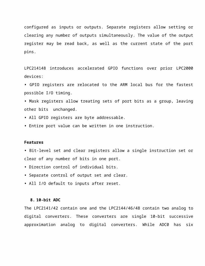
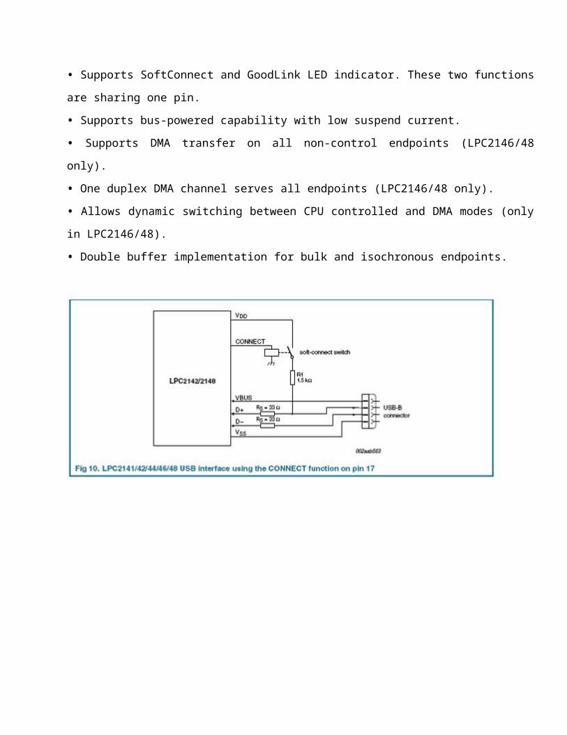
• Supports SoftConnect and GoodLink LED indicator. These two functions are sharing one pin.
• Supports bus-powered capability with low suspend current.
• Supports DMA transfer on all non-control endpoints (LPC2146/48 only).
• One duplex DMA channel serves all endpoints (LPC2146/48 only).
• Allows dynamic switching between CPU controlled and DMA modes (only in LPC2146/48).
• Double buffer implementation for bulk and isochronous endpoints.
11. UARTs
The LPC2141/42/44/46/48 each contains two UARTs. In addition to standard transmit and receive
data lines, the LPC2144/46/48 UART1 also provide a full modem control handshake interface.
Compared to previous LPC2000 microcontrollers, UARTs in LPC2141/42/44/46/48 introduce a
fractional baud rate generator for both UARTs, enabling these microcontrollers to achieve standard
baudrates such as 115200 with any crystal frequency above 2 MHz. In addition, auto-CTS/RTS flow-
control functions are fully implemented in hardware (UART1 in LPC2144/46/48 only).
11.1 Features
• 16 byte Receive and Transmit FIFOs.
• Register locations conform to ‘550 industry standard.
• Receiver FIFO trigger points at 1, 4, 8, and 14 bytes
• Built-in fractional baud rate generator covering wide range of baud rates without a need for external
crystals of particular values.
• Transmission FIFO control enables implementation of software (XON/XOFF) flow control on both
UARTs.
• LPC2144/46/48 UART1 equipped with standard modem interface signals. This module also provides
full support for hardware flow control (auto-CTS/RTS).
12. I2C-bus serial I/O controller
The LPC2141/42/44/46/48 each contain two I2C-bus controllers. The I2C-bus is bidirectional,
for inter-IC control using only two wires: a serial clock line (SCL), and a serial data line (SDA). Each
device is recognized by a unique address and can operate as either a receiver-only device (e.g., an LCD
driver or a transmitter with the capability to both receive and send information (such as memory)).
Transmitters and/or receivers can operate in either master or slave mode, depending on whether the chip
has to initiate a data transfer or is only addressed. The I2C-bus is a multi-master bus, it can be controlled
by more than one bus master connected to it. The I2C-bus implemented in LPC2141/42/44/46/48
supports bit rates up to 400 kbit/s (Fast I2C-bus).
12.1 Features
• Compliant with standard I2C-bus interface.
• Easy to configure as master, slave, or master/slave.
• Programmable clocks allow versatile rate control.
• Bidirectional data transfer between masters and slaves.
• Multi-master bus (no central master).
• Arbitration between simultaneously transmitting masters without corruption of serial data on the bus.
• Serial clock synchronization allows devices with different bit rates to communicate via one serial bus.
• Serial clock synchronization can be used as a handshake mechanism to suspend and resume serial
transfer.
• The I2C-bus can be used for test and diagnostic purposes.
13. SPI serial I/O controller
The LPC2141/42/44/46/48 each contain one SPI controller. The SPI is a full duplex serial
interface, designed to handle multiple masters and slaves connected to a given bus. Only a single master
and a single slave can communicate on the interface during a given data transfer. During a data transfer
the master always sends a byte of data to the slave, and the slave always sends a byte of data to the
master.
13.1 Features
• Compliant with Serial Peripheral Interface (SPI) specification.
• Synchronous, Serial, Full Duplex, Communication.
• Combined SPI master and slave.
• Maximum data bit rate of one eighth of the input clock rate.
14. SSP serial I/O controller
The LPC2148 contains one SSP. The SSP controller is capable of operation on a SPI, 4-wire SSI,
or Microwire bus. It can interact with multiple masters and slaves on the bus. However, only a single
master and a single slave can communicate on the bus during a given data transfer. The SSP supports
full duplex transfers, with data frames of 4 bits to 16 bits of data flowing from the master to the slave
and from the slave to the master. Often only one of these data flows carries meaningful data.
14.1 Features
• Compatible with Motorola’s SPI, TI’s 4-wire SSI and National Semiconductor’s Microwire buses.
• Synchronous serial communication.
• Master or slave operation.
• 8-frame FIFOs for both transmit and receive.
• Four bits to 16 bits per frame.
15. General purpose timers/external event counters
The Timer/Counter is designed to count cycles of the peripheral clock (PCLK) or an externally
supplied clock and optionally generate interrupts or perform other actions at specified timer values,
based on four match registers. It also includes four capture inputs to trap the timer value when an input
signal transition, optionally generating an interrupt. Multiple pins can be selected to perform a single
capture or match function, providing an application with ‘or’ and ‘and’, as well as ‘broadcast’ functions
among them. The LPC2141/42/44/46/48 can count external events on one of the capture inputs if the
minimum external pulse is equal or longer than a period of the PCLK. In this configuration, unused
capture lines can be selected as regular timer capture inputs, or used as external interrupts.
15.1 Features
• A 32-bit timer/counter with a programmable 32-bit prescaler.
• External event counter or timer operation.
• Four 32-bit capture channels per timer/counter that can take a snapshot of the timer value when an
input signal transitions. A capture event may also optionally generate an interrupt.
• Four 32-bit match registers that allow:
– Continuous operation with optional interrupt generation on match.
– Stop timer on match with optional interrupt generation.
– Reset timer on match with optional interrupt generation.
• Four external outputs per timer/counter corresponding to match registers, with the following
capabilities:
– Set LOW on match.
– Set HIGH on match.
– Toggle on match.
– Do nothing on match.
16. Watchdog timer
The purpose of the watchdog is to reset the microcontroller within a reasonable amount of time if it
enters an erroneous state. When enabled, the watchdog will generate a system reset if the user program
fails to ‘feed’ (or reload) the watchdog within a predetermined amount of time.
16.1 Features
• Internally resets chip if not periodically reloaded.
• Debug mode.
• Enabled by software but requires a hardware reset or a watchdog reset/interrupt to be disabled.
• Incorrect/Incomplete feed sequence causes reset/interrupt if enabled.
• Flag to indicate watchdog reset.
• Programmable 32-bit timer with internal pre-scaler.
• Selectable time period from (TPCLK × 256 × 4) to (TPCLK × 232 × 4) in multiples of TPCLK × 4.
17. Real-time clock
The RTC is designed to provide a set of counters to measure time when normal or idle operating mode is
selected. The RTC has been designed to use little power, making it suitable for battery powered systems
where the CPU is not running continuously (Idle mode).
17.1 Features
• Measures the passage of time to maintain a calendar and clock.
• Ultra-low power design to support battery powered systems.
• Provides Seconds, Minutes, Hours, Day of Month, Month, Year, Day of Week, and Day of Year.
• Can use either the RTC dedicated 32 kHz oscillator input or clock derived from the external
crystal/oscillator input at XTAL1. Programmable reference clock divider allows fine adjustment of the
RTC.
• Dedicated power supply pin can be connected to a battery or the main 3.3 V.
18. Pulse width modulator

The PWM is based on the standard timer block and inherits all of its features, although only the PWM
function is pinned out on the LPC2141/42/44/46/48. The timer is designed to count cycles of the
peripheral clock (PCLK) and optionally generate interrupts or perform other actions when specified
timer values occur, based on seven match registers. The PWM function is also based on match register
events. The ability to separately control rising and falling edge locations allows the PWM to be used for
more applications. For instance, multi-phase motor control typically requires three non-overlapping
PWM outputs with individual control of all three pulse widths and positions. Two match registers can be
used to provide a single edge controlled PWM output.
One match register (MR0) controls the PWM cycle rate, by resetting the count upon match. The other
match register controls the PWM edge position. Additional single edge controlled PWM outputs require
only one match register each, since the repetition rate is the same for all PWM outputs. Multiple single
edge controlled PWM outputs will all have a rising edge at the beginning of each PWM cycle, when an
MR0 match occurs. Three match registers can be used to provide a PWM output with both edges
controlled. Again, the MR0 match register controls the PWM cycle rate. The other match registers
control the two PWM edge positions. Additional double edge controlled PWM outputs require only two
match registers each, since the repetition rate is the same for all PWM outputs. With double edge
controlled PWM outputs, specific match registers control the rising and falling edge of the output. This
allows both positive going PWM pulses (when the rising edge occurs prior to the falling edge), and
negative going PWM pulses (when the falling edge occurs prior to the rising edge).
18.1 Features
• Seven match registers allow up to six single edge controlled or three double edge controlled PWM
outputs, or a mix of both types.
• The match registers also allow:
– Continuous operation with optional interrupt generation on match.
– Stop timer on match with optional interrupt generation.
– Reset timer on match with optional interrupt generation.
• Supports single edge controlled and/or double edge controlled PWM outputs. Single edge controlled
PWM outputs all go HIGH at the beginning of each cycle unless the output is a constant LOW. Double
edge controlled PWM outputs can have either edge occur at any position within a cycle. This allows for
both positive going and negative going pulses.
• Pulse period and width can be any number of timer counts. This allows complete flexibility in the
trade-off between resolution and repetition rate. All PWM outputs will occur at the same repetition rate.
• Double edge controlled PWM outputs can be programmed to be either positive going or negative going
pulses.
• Match register updates are synchronized with pulse outputs to prevent generation of erroneous pulses.
Software must ‘release’ new match values before they can become effective.
• May be used as a standard timer if the PWM mode is not enabled.
• A 32-bit Timer/Counter with a programmable 32-bit Prescaler.
19. System control
19.1 Crystal oscillator
On-chip integrated oscillator operates with external crystal in range of 1 MHz to 25 MHz. The oscillator
output frequency is called fosc and the ARM processor clock frequency is referred to as CCLK for
purposes of rate equations, etc. fosc and CCLK are the same value unless the PLL is running and
connected. Refer to Section 6.19.2 “PLL” for additional information.
19.2 PLL
The PLL accepts an input clock frequency in the range of 10 MHz to 25 MHz. The input frequency is
multiplied up into the range of 10 MHz to 60 MHz with a Current Controlled Oscillator (CCO). The
multiplier can be an integer value from 1 to 32 (in practice, the multiplier value cannot be higher than 6
on this family of microcontrollers due to the upper frequency limit of the CPU). The CCO operates in
the range of 156 MHz to 320 MHz, so there is an additional divider in the loop to keep the CCO within
its frequency range while the PLL is providing the desired output frequency. The output divider may be
set to divide by 2, 4, 8, or 16 to produce the output clock. Since the minimum output divider value is 2,
it is insured that the PLL output has a 50 % duty cycle. The PLL is turned off and bypassed following a
chip reset and may be enabled by software. The program must configure and activate the PLL, wait for
the PLL to Lock, then connect to the PLL as a clock source. The PLL settling time is 100 μs.
19.3 Reset and wake-up timer
Reset has two sources on the LPC2141/42/44/46/48: the RESET pin and watchdog reset. The RESET
pin is a Schmitt trigger input pin with an additional glitch filter. Assertion of chip reset by any source
starts the Wake-up Timer (see Wake-up Timer description below), causing the internal chip reset to
remain asserted until the external reset is de-asserted, the oscillator is running, a fixed number of clocks
have passed, and the on-chip flash controller has completed its initialization. When the internal reset is
removed, the processor begins executing at address 0, which is the reset vector. At that point, all of the
processor and peripheral registers have been initialized to predetermined values.
The Wake-up Timer ensures that the oscillator and other analog functions required for chip operation are
fully functional before the processor is allowed to execute instructions. This is important at power on, all
types of reset, and whenever any of the aforementioned functions are turned off for any reason. Since
the oscillator and other functions are turned off during Power-down mode, any wake-up of the processor
from Power-down mode makes use of the Wake-up Timer.
The Wake-up Timer monitors the crystal oscillator as the means of checking whether it is safe to begin
code execution. When power is applied to the chip, or some event caused the chip to exit Power-down
mode, some time is required for the oscillator to produce a signal of sufficient amplitude to drive the
clock logic. The amount of time depends on many factors, including the rate of VDD ramp (in the case
of power on), the type of crystal and its electrical characteristics (if a quartz crystal is used), as well as
any other external circuitry (e.g. capacitors), and the characteristics of the oscillator itself under the
existing ambient conditions.
19.4 Brownout detector
The LPC2141/42/44/46/48 includes 2-stage monitoring of the voltage on the VDD pins. If this voltage
falls below 2.9 V, the BOD asserts an interrupt signal to the VIC. This signal can be enabled for
interrupt; if not, software can monitor the signal by reading dedicated register. The second stage of low
voltage detection asserts reset to inactivate the LPC2141/42/44/46/48 when the voltage on the VDD pins
falls below 2.6 V. This reset prevents alteration of the flash as operation of the various elements of the
chip would otherwise become unreliable due to low voltage. The BOD circuit maintains this reset down
below 1 V, at which point the POR circuitry maintains the overall reset. Both the 2.9 V and 2.6 V
thresholds include some hysteresis. In normal operation, this hysteresis allows the 2.9 V detection to
reliably interrupt, or a regularly-executed event loop to sense the condition.
19.5 Code security
This feature of the LPC2148 allows an application to control whether it can be debugged or protected
from observation. If after reset on-chip boot loader detects a valid checksum in flash and reads 0x8765
4321 from address 0x1FC in flash, debugging will be disabled and thus the code in flash will be
protected from observation. Once debugging is disabled, it can be enabled only by performing a full chip
erase using the ISP.
19.6 External interrupt inputs
The LPC2141/42/44/46/48 include up to nine edge or level sensitive External Interrupt Inputs as
selectable pin functions. When the pins are combined, external events can be processed as four
independent interrupt signals. The External Interrupt Inputs can optionally be used to wake-up the
processor from Power-down mode. Additionally capture input pins can also be used as external
interrupts without the option to wake the device up from Power-down mode.
19.7 Memory mapping control
The Memory Mapping Control alters the mapping of the interrupt vectors that appear beginning at
address 0x0000 0000. Vectors may be mapped to the bottom of the on-chip flash memory, or to the on-
chip static RAM. This allows code running in different memory spaces to have control of the interrupts.
19.8 Power control
The LPC2141/42/44/46/48 supports two reduced power modes: Idle mode and Power-down mode. In
Idle mode, execution of instructions is suspended until either a reset or interrupt occurs. Peripheral
functions continue operation during Idle mode and may generate interrupts to cause the processor to
resume execution. Idle mode eliminates power used by the processor itself, memory systems and related
controllers, and internal buses. In Power-down mode, the oscillator is shut down and the chip receives
no internal clocks. The processor state and registers, peripheral registers, and internal SRAM values are
preserved throughout Power-down mode and the logic levels of chip output pins remain static.
The Power-down mode can be terminated and normal operation resumed by either a reset or certain
specific interrupts that are able to function without clocks. Since all dynamic operation of the chip is
suspended, Power-down mode reduces chip power consumption to nearly zero. Selecting an external 32
kHz clock instead of the PCLK as a clock-source for the on-chip RTC will enable the microcontroller to
have the RTC active during Power-down mode. Power-down current is increased with RTC active.
However, it is significantly lower than in Idle mode. A Power Control for Peripherals feature allows
individual peripherals to be turned off if they are not needed in the application, resulting in additional
power savings during active and idle mode.
19.9 VPB bus
The VPB divider determines the relationship between the processor clock (CCLK) and the clock used by
peripheral devices (PCLK). The VPB divider serves two purposes. The first is to provide peripherals
with the desired PCLK via VPB bus so that they can operate at the speed chosen for the ARM processor.
In order to achieve this, the VPB bus may be slowed down to 1⁄2 to 1⁄4 of the processor clock rate.
Because the VPB bus must work properly at power-up (and its timing cannot be altered if it does not
work since the VPB divider control registers reside on the VPB bus), the default condition at reset is for
the VPB bus to run at 1⁄4 of the processor clock rate. The second purpose of the VPB divider is to allow
power savings when an application does not require any peripherals to run at the full processor rate.
Because the VPB divider is connected to the PLL output, the PLL remains active (if it was running)
during Idle mode.
20. Emulation and debugging
The LPC2141/42/44/46/48 support emulation and debugging via a JTAG serial port. A trace port allows
tracing program execution. Debugging and trace functions are multiplexed only with GPIOs on Port 1.
This means that all communication, timer and interface peripherals residing on Port 0 are available
during the development and debugging phase as they are when the application is run in the embedded
system itself.
20.1 EmbeddedICE
Standard ARM EmbeddedICE logic provides on-chip debug support. The debugging of the target
system requires a host computer running the debugger software and an EmbeddedICE protocol
convertor. EmbeddedICE protocol convertor converts the remote debug protocol commands to the
JTAG data needed to access the ARM core. The ARM core has a Debug Communication Channel
(DCC) function built-in. The DCC allows a program running on the target to communicate with the host
debugger or another separate host without stopping the program flow or even entering the debug state.
The DCC is accessed as a co-processor 14 by the program running on the ARM7TDMI-S core. The
DCC allows the JTAG port to be used for sending and receiving data without affecting the normal
program flow. The DCC data and control registers are mapped in to addresses in the EmbeddedICE
logic.
20.2 Embedded trace
Since the LPC2141/42/44/46/48 have significant amounts of on-chip memory, it is not possible to
determine how the processor core is operating simply by observing the external pins. The Embedded
Trace Macrocell (ETM) provides real-time trace capability for deeply embedded processor cores. It
outputs information about processor execution to the trace port. The ETM is connected directly to the
ARM core and not to the main AMBA system bus. It compresses the trace information and exports it
through a narrow trace port. An external trace port analyzer must capture the trace information under
software debugger control. Instruction trace (or PC trace) shows the flow of execution of the processor
and provides a list of all the instructions that were executed. Instruction trace is significantly compressed
by only broadcasting branch addresses as well as a set of status signals that indicate the pipeline status
on a cycle by cycle basis. Trace information generation can be controlled by selecting the trigger
resource. Trigger resources include address comparators, counters and sequencers. Since trace
information is compressed the software debugger requires a static image of the code being executed.
Self-modifying code can not be traced because of this restriction.
20.3 RealMonitor
RealMonitor is a configurable software module, developed by ARM Inc., which enables real-time
debug. It is a lightweight debug monitor that runs in the background while users debug their foreground
application. It communicates with the host using the DCC, which is present in the EmbeddedICE logic.
The LPC2141/42/44/46/48 contain a specific configuration of RealMonitor software programmed into
the on-chip flash memory.
Related Documents