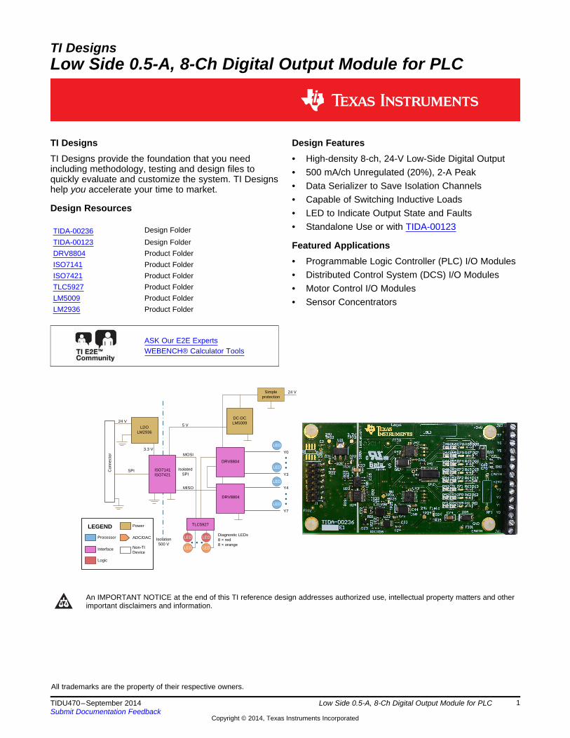
24 V Y0 ISO7141 ISO7421 LDO LM2936 SPI Connector 24 V 3.3 V Isolation 500 V DRV8804 Y3 Y7 Y4 DC-DC LM5009 5 V DRV8804 Isolated SPI Simple protection LE D MOSI MISO TLC5927 LE D Diagnostic LEDs 8 × red 8 × orange ^ ^ ^ ^ ^ ^ LED LED LED LED LED LED LED LED ^ ^ ^ Logic Processor Interface LEGEND Power ADC/DAC Non-TI Device TI Designs Low Side 0.5-A, 8-Ch Digital Output Module for PLC TI Designs Design Features TI Designs provide the foundation that you need • High-density 8-ch, 24-V Low-Side Digital Output including methodology, testing and design files to • 500 mA/ch Unregulated (20%), 2-A Peak quickly evaluate and customize the system. TI Designs • Data Serializer to Save Isolation Channels help you accelerate your time to market. • Capable of Switching Inductive Loads Design Resources • LED to Indicate Output State and Faults • Standalone Use or with TIDA-00123 Design Folder TIDA-00236 TIDA-00123 Design Folder Featured Applications DRV8804 Product Folder • Programmable Logic Controller (PLC) I/O Modules ISO7141 Product Folder • Distributed Control System (DCS) I/O Modules ISO7421 Product Folder TLC5927 Product Folder • Motor Control I/O Modules LM5009 Product Folder • Sensor Concentrators LM2936 Product Folder ASK Our E2E Experts WEBENCH® Calculator Tools An IMPORTANT NOTICE at the end of this TI reference design addresses authorized use, intellectual property matters and other important disclaimers and information. All trademarks are the property of their respective owners. 1 TIDU470 – September 2014 Low Side 0.5-A, 8-Ch Digital Output Module for PLC Submit Documentation Feedback Copyright © 2014, Texas Instruments Incorporated

Welcome message from author
This document is posted to help you gain knowledge. Please leave a comment to let me know what you think about it! Share it to your friends and learn new things together.
Transcript
24 V
Y0
ISO7141ISO7421
LDOLM2936
SPICon
nect
or
24 V
3.3 V
Isolation500 V
DRV8804
Y3
Y7
Y4
DC-DCLM50095 V
DRV8804
IsolatedSPI
Simpleprotection
LED
MOSI
MISO
TLC5927
LED
Diagnostic LEDs8 × red8 × orange
�
�
�
�
�
�LED
LED
LED
LED
LEDLED
LEDLED
���
Logic
Processor
Interface
LEGEND Power
ADC/DAC
Non-TIDevice
TI DesignsLow Side 0.5-A, 8-Ch Digital Output Module for PLC
TI Designs Design FeaturesTI Designs provide the foundation that you need • High-density 8-ch, 24-V Low-Side Digital Outputincluding methodology, testing and design files to • 500 mA/ch Unregulated (20%), 2-A Peakquickly evaluate and customize the system. TI Designs
• Data Serializer to Save Isolation Channelshelp you accelerate your time to market.• Capable of Switching Inductive Loads
Design Resources • LED to Indicate Output State and Faults• Standalone Use or with TIDA-00123Design FolderTIDA-00236
TIDA-00123 Design Folder Featured ApplicationsDRV8804 Product Folder
• Programmable Logic Controller (PLC) I/O ModulesISO7141 Product Folder• Distributed Control System (DCS) I/O ModulesISO7421 Product Folder
TLC5927 Product Folder • Motor Control I/O ModulesLM5009 Product Folder • Sensor ConcentratorsLM2936 Product Folder
ASK Our E2E ExpertsWEBENCH® Calculator Tools
An IMPORTANT NOTICE at the end of this TI reference design addresses authorized use, intellectual property matters and otherimportant disclaimers and information.
All trademarks are the property of their respective owners.
1TIDU470–September 2014 Low Side 0.5-A, 8-Ch Digital Output Module for PLCSubmit Documentation Feedback
Copyright © 2014, Texas Instruments Incorporated

Key System Specifications www.ti.com
1 Key System Specifications
Table 1. Key System Specifications
SPECIFICATIONSYMBOL PARAMETER CONDITIONS UNIT
MIN TYP MAXVIN Input voltage Normal operation 10 24 33 VIIN Input current Normal operation - 15 50 mA
VLOAD Load supply voltage Normal operation 0 24 44 VPer channel - 500 600 mATA = 60°C
ILOAD Load currentPer channel - 700 1000 mATA = 25°C
PLOSS Power loss per channel RL = 48 Ω, VLOAD = 24 V, TA = 25°C - 200 - mWResitive load 1000 Hz
fSW Switching frequency Inductive load, 10 Hz0.1 H all channelsLoad voltage rise timetRISE RL = 48 Ω, VLOAD = 24 V, TA = 25°C - 600 - ns10% .. 90%Load voltage fall timetFALL RL = 48 Ω, VLOAD = 24 V, TA = 25°C - 120 - ns90% .. 10%
tPD Propagation delay (latch to output change) RL = 48 Ω, VLOAD = 24 V, TA = 25°C - 150 - nsIPEAK Peak current (1 ms) 2.3 3.8 A
Inductive power for each group ofPIND 0.5 J/schannels (1)
(1) Outputs Y0 to Y3 are one group and outputs Y4 to Y7 are one group.
2 System DescriptionA digital output (DO) module is a standard module in a PLC or DCS system. The DO module is used topermanently turn on and off resistive, capacitive, or inductive loads or control them with pulse widthmodulation (PWM).
A digital output with a MOSFET can be realized as a high-side or low-side switch. This design uses thelow-side switch principal, which means that the load connected to the output between the 24-V supply andthe output of the module. Therefore, the switch is below the load seen from the 24-V DC supply.
The advantage with this principal is its lower cost of the switching MOSFETs as they can be of NMOStype, which are smaller compared to a PMOS FET with the same Rds(on) and does not need a voltageabove the supply voltage to operate the FET in the saturated region. A low-side configuration is on theother hand more sensitive to corrosion as the load is permanently connected to a 24-V supply even whenswitched off. This configuration also means that a short to ground turns on the load unintentionally.
In most cases, the digital outputs are galvanic isolated from the control of the outputs. This design useslow power digital isolators to separate the 24-V field supply from the SPI control signals. The use of SPIas a control interface reduces the number of isolated channels from eight channels to four. The field sidealso has a high efficiency power supply from 24-V DC to power the digital isolators, the LED driver, andstatus LEDs.
The form factor of the board and the connector enables the TIDA-00236 to be used with TIDA-00123 anduse the onboard microcontroller (MCU) to control the outputs. The board can also be used alone and usethe standard connector on the top side to connect it to any MCU or microprocessor (MPU) capable ofhandling SPI communication.
2 Low Side 0.5-A, 8-Ch Digital Output Module for PLC TIDU470–September 2014Submit Documentation Feedback
Copyright © 2014, Texas Instruments Incorporated

24 V
Y0
ISO7141ISO7421
LDOLM2936
SPICon
nect
or
24 V
3.3 V
Isolation500 V
DRV8804
Y3
Y7
Y4
DC-DCLM50095 V
DRV8804
IsolatedSPI
Simpleprotection
LED
MOSI
MISO
TLC5927
LED
Diagnostic LEDs8 × red8 × orange
�
�
�
�
�
�LED
LED
LED
LED
LEDLED
LEDLED
���
Logic
Processor
Interface
LEGEND Power
ADC/DAC
Non-TIDevice
www.ti.com Block Diagram
3 Block Diagram
Figure 1. Simplified Block Diagram
3.1 Highlighted ProductsThe TIDA-00236 has eight digital outputs configured as low side drivers. The design uses two DRV8804with four protected low-side drivers integrated in each device. The on-chip shift register control logicmakes it possible to control the output through SPI and also daisy chain multiple devices (in this case,two). Compared to a paralleled control approach, this saves isolation channels as one SPI channel (fourlines) can control eight output channels or more. The ISO7141 provides galvanic isolation for the SPIchannel. Each DRV8804 also has a global fault pin, which indicates fault on any of the four outputchannels. Those signals are connected to the ISO7421, which galvanic isolates the signal. LM5009 isused in a low-cost buck configuration to provide 5 V to power the secondary side of the ISO7141 andISO7421. The 5 V is also used for the TLC5927 including LEDs. The LED lighting driver TLC5927 drivesto two programmable status LEDs per output, 16 in total. An additional eight status LEDs are connected tothe outputs of the DRV8804s and indicates the physical status of the output. The LM2936 is a low-costlow dropout (LDO) to supply the primary side of the ISO7141 and ISO7421 with 3.3 V.
3TIDU470–September 2014 Low Side 0.5-A, 8-Ch Digital Output Module for PLCSubmit Documentation Feedback
Copyright © 2014, Texas Instruments Incorporated

Thermal
Shut down
OUT1
GND
(multiple pins)
VCLAMP
LATCH
SDATIN
SCLK
Internal
Reference
Regs
UVLO
Int. VCC
nFAULT
Control
Logic
RESET
nENBL
VMLS Gate
Drive
OUT2
OUT3
OUT4
OCP
&
Gate
Drive
8.2V – 60V
OCP
&
Gate
Drive
OCP
&
Gate
Drive
OCP
&
Gate
Drive
8.2V – 60VOptional
Zener
Inductive
Load
Inductive
Load
Inductive
Load
Inductive
Load
SDATOUT
Block Diagram www.ti.com
3.1.1 DRV8804
Figure 2. DRV8804 Functional Block Diagram
The DRV8804 is a four-channel low-side driver with overcurrent protection in combination with built-inclamping diodes makes it suitable for driving resistive, capacitive, or inductive loads. The control logicprovides an SPI interface, which can daisy chain multiple devices. The DRV8803 has similar functionalitybut with a parallel interface instead of SPI, so this design could be used for evaluating thermal and drivingperformance of that device as well.
Internal shutdown functions are provided for overcurrent protection, short circuit protection, undervoltagelockout, and over temperature and are all connected to the nFAULT pin.
3.1.2 ISO7141 and ISO7421The ISO7141 and ISO7421 provide galvanic isolation at 2500 VRMS for one minute per UL or 4242 VPK perVDE. The ISO7141 offers three channels in the forward direction and one back channel, which makes itsuitable for SPI communication isolation. The ISO7421 has one forward and one backward channel and isused to isolate the /XFAULT signal. The ISO7141 can work up to 50 Mbps, which is well above the SPIcommunication speed used in this design. The ISO7421 is slower but still fast enough to support theslower speed signals /XFAULT and RST.
3.1.3 LM5009The LM5009 is a wide-input, step down non-synchronous converter with integrated FET. This design hasa 5-V regulated output from the 24-V field connector to supply the ISO7141, ISO7421, and the LED driverincluding LEDs.
4 Low Side 0.5-A, 8-Ch Digital Output Module for PLC TIDU470–September 2014Submit Documentation Feedback
Copyright © 2014, Texas Instruments Incorporated

www.ti.com System Design Theory
3.1.4 TLC5927The TLC5927 is designed for LED lighting applications with open-load, shorted-load, over-temperaturedetection, and constant-current control. The TLC5927 contains a 16-bit shift register and data latches,which convert serial input data into parallel output format. At the TLC5927 output stage, 16 regulated-current ports provide uniform and constant current for driving LEDs.
4 System Design TheoryThe ISO7141 isolates the host from the field side for the SPI signals. The ISO7141 is a very fast isolator,and data speeds up to 1 Mbps can easily be supported. Therefore, a large number of outputs cancontrolled over this interface. At 1 Mbps, it is theoretically possible to control up to 250 output signals at arefresh rate of 4 kHz. This small form factor design demonstrates eight outputs and an additional 16diagnostic LEDs, requiring in total 24 output signals. Given those requirements up to 64 outputs with thesame control technique are feasible. The design is fully static and for diagnostic purposes the serial shiftclock can go as low as DC.
4.1 Low-Side Driver SelectionTo demonstrate the small form factor, this design uses two DRV8804. These devices integrate four poweroutputs in a PWP package at 5×7-mm board space and are capable of simultaneously driving 0.5 A ateach output with only PCB cooling. An area of about 15 cm2 would be sufficient for operation at ambienttemperatures of 85°C. The DRV8804s provide internal diodes to a common clamping pin, which allowssetting a clamping voltage different from the operating voltage for fast inductive discharge. The dischargethen happens in an external Zener diode (D57 and D58). The power capability of the Zener diodes definesthe quantity of inductive discharge the module can handle and can be set application specific. The TIDA-00236 uses a clamp of 48 V and the Zener diodes can dissipate 3 W each. Therefore, an inductivedischarge of 750 mJ can occur once each second for each output.
4.2 Thermal ManagementThe thermal management budget has been calculated based on the following design considerations:• The junction temperature should not surpass 150°C• The thermal resistance of the package is 2.3 K/W junction to bottom plate• The thermal vias have an inner diameter of 8 mil and capable of 170 K/W• Board space provides thermal resistance to air of around 900 K/W per cm2 (see formula 23 in
Reference 2)
The RDS(ON) of the DRV8804 is max 0.8 Ω and with four outputs turned on at 0.5 A the total powerdissipation is 0.8 W per device (4 × 0.52 × 0.8). For an ambient temperature of 60°C, the junctiontemperature increases 90 K. Therefore, TIDA-00236 has 15 thermal vias per device, which results in a 11-K/W resistance and 9-K temperature increase on top of the 1.8-K junction case rise. Consequently, thecopper area temperature increases with 89 K. The copper area therefore needs a thermal resistance to airof 110 K/W, which is equivalent to 8.2 cm2. The TIDA-00236 has approximately 10 cm2 available perDRV8804.
Use a four-layer board if an ambient temperature beyond 85°C is desired. Therefore, the cooling areacould be increased to 15 cm2 on each side of the PCB, in total 30 cm2 per DRV8804.
5TIDU470–September 2014 Low Side 0.5-A, 8-Ch Digital Output Module for PLCSubmit Documentation Feedback
Copyright © 2014, Texas Instruments Incorporated

System Design Theory www.ti.com
4.3 Switch Off an Inductive LoadThe TIDA-00236 can be used to switch off inductive loads like motors, valves, and so on. An inductiveload has the property that it stores energy. This energy releases when the switch wants to turn theinductive load off. The inductor tries to keep the current flowing, which could result in a high voltage spikeat the output of the switch. Typical methods to prevent the occurrence of spikes are freewheeling diodes.These diodes limit the voltage at the inductor so that it does not exceed the diode forward voltage oftypical 0.7 V. The resulting voltage at the output of the switch would be 24.7 V assuming a power supplyof 24 V. The method is simple but it has the disadvantage the current keeps flowing for some period oftime. The time is reverse proportional to the freewheeling voltage. For high-speed actuators like injectionvalves in process control systems, this is not desired. The preferred method is to use a Zener diode sothat the freewheeling voltage can be higher. In this reference design, the freewheeling voltage is clampedto 48 V. At a 24-V supply, this clamping results in a freewheeling voltage of 24 V and a much faster decayof the inductor current. Therefore, this reference design is best suited for direct control of stepper motorsor injection valves.
The DRV8804 has protected the low-side switches with one integrated clamping diode per each output. Allclamping diodes are fed to one pin for an external Zener diode. This diode clamps the voltage to 48 V.
The external Zener diodes (D57 and D58) in the TIDA-0023 is a 3-W TVS diode with cooling calculated for500 mW, meaning all outputs of one DRV8804 can absorb 0.5 J/s of energy. An inductive load of 100 mHcan store around 12.5 mJ (E = ½ × L × I2) at a current of 0.5 A. The load could therefore switch at a rateof 40 Hz for one output or 10 Hz if all four outputs are loaded and switched.
4.4 Switching Light BulbsThe TIDA-00236 can be used to switch conventional light bulbs. Such a load has a very low coldresistance, so the initial current can be as much as 10 times higher than the continuous current. A 24-V,5-W light bulb has an in-rush current of 2 A, which is within the operating range of the DRV8804. Largerlight bulbs trigger the overcurrent protection. Such a light bulb would not harm the DRV8804, but the lightbulb might not turn on as desired.
6 Low Side 0.5-A, 8-Ch Digital Output Module for PLC TIDU470–September 2014Submit Documentation Feedback
Copyright © 2014, Texas Instruments Incorporated

/CS0
SCLK
MISO
MOSI
+24V
+3.3V
/XFAULT
XRST
1 2
3 4
5 6
7 8
9 10
11 12
13 14
J1
TSM-107-02-L-DV-P
GPIO0
GPIO1
GPIO2
EVM_ID_SCL
/XFAULT
/CS0
SCLK
MISO
MOSI
EVM_ID_SDA
XRST
+24V+24V
1 2
3 4
5 6
7 8
9 10
11 12
13 14
15 16
17 18
19 20
21 22
23 24
25 26
27 28
29 30
31 32
33 34
35 36
37 38
39 40
41 42
43 44
45 46
47 48
49 50
MH1
MH2
J2
ERF8-025-05.0-L-DV-K-TR
GPIO0
GPIO1
GPIO2
www.ti.com Getting Started Hardware
5 Getting Started HardwareThe TIDA-00236 can be used either as a plug-in card in the TIDA-00123 PLC evaluation platform or as astandalone card with any processor capable of handling SPI communication. For the connection to theTIDA-00123 platform, the connector J2 handles the communication.
Figure 3. Connector J2 (Bottom Side)
The connector, J1, on the top side of the board, is a 14-pol connector that can connect the board to anyprocessor platform with a standard flat cable.
Figure 4. Connector J1 (Top Side)
7TIDU470–September 2014 Low Side 0.5-A, 8-Ch Digital Output Module for PLCSubmit Documentation Feedback
Copyright © 2014, Texas Instruments Incorporated

Getting Started Hardware www.ti.com
The pins described in Table 2 have to be connected to the connector J1 of the TIDA-00236 tocommunicate with the card.
Table 2. Pin Description J1
J1 SIGNALS DESCRIPTIONChip select / latch: rising edge to transfer2 /CS0 data to outputs Y0 to Y7
4 SCLK Serial clock7 XRST Reset: high to reset the outputs
Master Out Slave In: Data to be sent to8 MOSI the digital output card13 24 V 5 to 24 V host-side power14 GND Ground signal
5.1 SPI InterfaceThe implemented serial is a standard SPI interface with all four channels implemented. The processorconnected to the board will have to act as SPI master and provide the clock on the SCLK pin.
Table 3. SPI Signal Connections
PIN DESCRIPTION POSITION ON J1 POSITION ON J2Serial Clock (output fromSCLK 4 3master)
MOSI Master Output, Slave Input 8 7MISO Master Input, Slave Output 6 5
Chip Select and Latch (active/CS0 low, data transferred to outputs 2 1
Y0 to Y7 with rising edge).
When driven high, the XRST pin (pin 7 on J1 and pin 26 on J2) resets all internal logic and all DRV8804registers are cleared.
5.2 Fault SignalThe /XFAULT (pin 5 on J1 and pin 6 on J2) is a global fault signal for any of the eight outputs. The pin isdriven low in the case of an overcurrent event in any of the DRV8804s. At the same time, the driver withan overcurrent event is turned off. The driver remains turned off for about 1.2 ms before it retries to startand clear the fault signal. /XFAULT also is cleared if the XRST pin is activated or the 24-V field supply isremoved (J61 or J62).
If the die temperature in the DRV8804s exceeds safe limits, all output is switched off and the /XFAULT isdriven low. Operation will resume when the temperature falls under the limit.
5.3 Power SupplyFor the board to operate a 24-V power supply needs to be supplied to the pin 35, 36, 37 or 38 on theconnector J2 or pin 13 on connector J1. The ground needs to be connected according to Figure 3 orFigure 4 depending on which connector is in use. This power supplies the primary side of the ISO7141and ISO7421 over the LM2936.
5.4 Output and Field Power ConnectorIn the connector J61 and J62, connect 24 V and the ground to the labeled screw terminals. The eightloads can be connected between 24 V and the eight outputs labeled as Y7 to Y0 on the connectors J61and J62. Earth on J61 and J62 is connected to machine earth.
8 Low Side 0.5-A, 8-Ch Digital Output Module for PLC TIDU470–September 2014Submit Documentation Feedback
Copyright © 2014, Texas Instruments Incorporated

www.ti.com Getting Started Firmware
6 Getting Started FirmwareThe TIDA-00236_demo_code.c is a SPI driver in c-code that, with small modifications, can be compiled onmost MCU and MPU platforms. The most important sectors of the code are described in the followingsections.
6.1 Data BitsDB23:DB0 is sent to the digital output card through software controlled SPI. DB23:DB16 corresponds tooutput Y7-Y0. DB15:DB0 corresponds to the eight red LEDs (D49 to D56) and the eight orange LEDs(D41 to D48) interleaved as shown in Table 4.
Table 4. Data Bits (DB23:DB0) with Corresponding Function
Data Bits (DB23:DB0)23 22 21 20 19 18 17 16 15 14 13 12 11 10 9 8 7 6 5 4 3 2 1 0Y7 Y6 Y5 Y4 Y3 Y2 Y1 Y0 R7 O7 R6 O6 R5 O5 R4 O4 R3 O3 R2 O2 R1 O1 R0 O0
The sequence for sending DB23:DB0 is as follows:1. Assert XRST (pin 7 on J1 or pin 26 on J2) to reset the card and de-assert the pin.2. Assert /CS0 (pin 2 on J1 or pin 1 on J2) to enable the card.3. Set SCLK (pin 4 on J1 or pin 3 on J2) to LOW Put DB23:DB0 on MOSI (pin 8 on J1 or pin 7 on J2)
starting with MSB (DB23) and make SCLK HIGH. Repeat this for DB23:DB0 in total 24 times to shiftout all data bits.
Figure 5. Data Bits Transfer Pattern
6.2 GPIO for SPIThe code assumes a port on address 0x100 (variable IOPort). For the SPI communication, the GPIOs arelisted in Table 5.
Table 5. GPIOs used for SPI
SPI SIGNAL SCLK MOSI MISO /CS XRST /XFAULTPORT PIN 0 1 2 3 4 5
If another port and pins are used the addresses in the variable IOPort and Pin_Masks should be changedaccordingly. In the code, set the output (Y7 to Y0) one by one and check the /XFAULT pin. If /XFAULT ishigh, then switch on the red LEDs (D49 to D56).
The MOSI is not used in this code example. In other words, there is no SPI data transfer from the card tothe controller side.
9TIDU470–September 2014 Low Side 0.5-A, 8-Ch Digital Output Module for PLCSubmit Documentation Feedback
Copyright © 2014, Texas Instruments Incorporated

Y6
Y5
Y4
GND
Earth
Y2
Y0
+24V
Y3
Y1
GND
Earth
Y7
+24V
48 0 to 33 V
V
+
±
48
48
48
+±
DC
Test Setup www.ti.com
7 Test Setup
7.1 Output Current CapabilityThe GW inSTEK GPS-4303 quad-output DC power supplies are:• Two 0 to 30 V at up to 3A• One 8 to 15 V at 1 A• One 2.2 to 5.5 V at 1 A
All four outputs of one group (Y0 to Y3 or Y4 to Y7) are connected via individual 48-Ω, 12-W resistors to24 V of the power supply. GND and Earth are connected to 0 V of the power supply. Then all outputs areprogrammed to turn on. The current from the power supply into the resistors should read 2 A. Thetemperature of the driving switch is observed and settle around 50°C at a room temperature of 25°C. Thedrop voltage over the switch should be around 250 mV.
Figure 6. Measurement Setup for Over- and Undervoltage Lockout
10 Low Side 0.5-A, 8-Ch Digital Output Module for PLC TIDU470–September 2014Submit Documentation Feedback
Copyright © 2014, Texas Instruments Incorporated

Y6
Y5
Y4
GND
Earth
Y2
Y0
+24V
Y3
Y1
GND
Earth
Y7
+24V
Oscilloscope
48
0 to 33 V
+24V
GND
GND
GND
+3.3V
MOSI
MISO
SCLK
/CS0
GPIO2
XRST
/XFAULT
GPIO1
GPIO0
Ch 1
Ch 2
+±
48
48
48
www.ti.com Test Setup
7.2 Rise and Fall Times, Propagation DelayThe GW inSTEK GPS-4303 quad-output DC power supplies are:• Two 0 to 30 V at up to 3A• One 8 to 15 V at 1 A• One 2.2 to 5.5 V at 1 A• Oscilloscope: Tektronix TDS 3034
All four outputs of one group (Y4 to Y7) are connected via individual 48-Ω, 12-W resistors to 24 V of thepower supply. GND and Earth are connected to 0 V of the power supply. The oscilloscope is connected tothe latch input on the host side with channel one and to output Y7 with channel two. It is set to normaltrigger rising edge with the trigger coming from channel one. The trigger level is 1 V. Then all outputs areprogrammed to turn on. The oscilloscope captures a falling edge on Y7. Afterwards, all outputs areprogrammed to turn off, and the oscilloscope captures a rising edge on Y7. The measurement is repeatedwith the other three outputs of the same group. Then the resistors are connected to the second group ofoutputs (Y0 to Y3) and the measurement continues on these.
Figure 7. Measurement Setup for Rise and Fall Times and Propagation Delay
11TIDU470–September 2014 Low Side 0.5-A, 8-Ch Digital Output Module for PLCSubmit Documentation Feedback
Copyright © 2014, Texas Instruments Incorporated

Test Data www.ti.com
8 Test Data
Table 6. Test Results
SPECIFICATIONSYMBOL PARAMETER CONDITIONS MEAS. UNIT
MIN TYP MAXVIN Input voltage Normal operation 10 24 33 24.5 VIIN Input current Normal operation - 15 50 (1) 14 mA
VLOAD Load supply voltage Normal operation 0 24 44 24.5 VPer channel - 500 600 - (2) mATA = 60°C
ILOAD Load currentPer channel - 700 1000 - (2) mATA = 25°C
PLOSS Power loss per channel RL = 48 Ω, VLOAD = 24 V, TA = 25°C - 200 - - (2) mWResitive load 1000 1000 Hz
fSW Switching frequency Inductive load, 10 - (2) Hz0.1 H all channelsLoad voltage rise timetRISE RL = 48 Ω, VLOAD = 24 V, TA = 25°C - 600 - 550 ns10% .. 90%Load voltage fall timetFALL RL = 48 Ω, VLOAD = 24 V, TA = 25°C - 120 - 125 ns90% .. 10%
Propagation Delay (latch totPD RL = 48 Ω, VLOAD = 24 V, TA = 25°C 60 150 200 165 nsoutput change)IPEAK Peak current (1ms) 2.3 3.8 - (2) A
Inductive power for eachPIND 0.5 - (2) J/sgroup of channels (3)
(1) Depends on number of LEDs on and communication activity(2) Based on calculations derived from DRV8804 datasheet(3) Outputs Y0 to Y3 are one group and outputs Y4 to Y7 are one group
12 Low Side 0.5-A, 8-Ch Digital Output Module for PLC TIDU470–September 2014Submit Documentation Feedback
Copyright © 2014, Texas Instruments Incorporated

www.ti.com Test Data
In Figure 8 and Figure 9, channel 3 (purple) is connected to the /CS0 signal of the host connector andtriggers on the rising edge. This edge causes the data to transfer to the outputs Y0 to Y7 and is thereforebest suited to capture the output transitions (channel 4, green) and the timings for the propagation delaymeasurement. The fall time is dominated by the switching speed of the output transistor in the driver. Dueto the open drain configuration, the rise time results from the RC combination formed by the 10-nFcapacitor connected to the switch output in the reference design, the driver output capacitance and the 48-Ω load resistor at the output.
Figure 8. Fall Time Figure 9. tPD Falling Edge
Figure 10. Rise Time Figure 11. tPD Rising Edge
13TIDU470–September 2014 Low Side 0.5-A, 8-Ch Digital Output Module for PLCSubmit Documentation Feedback
Copyright © 2014, Texas Instruments Incorporated

EVM_ID_SCL
/XFAULT
/CS0
SCLK
MISO
MOSI
EVM_ID_SDA
XRST
+24V+24V
+3.3V
1 2
3 4
5 6
7 8
9 10
11 12
13 14
15 16
17 18
19 20
21 22
23 24
25 26
27 28
29 30
31 32
33 34
35 36
37 38
39 40
41 42
43 44
45 46
47 48
49 50
MH1
MH2
J2
ERF8-025-05.0-L-DV-K-TR
EVM_ID_SCL
EVM_ID_SDA
MISO
MOSI
SCLK
/CS0
/XFAULT
XRST
A01
A12
A23
VSS4
SDA5
SCL6
WP7
VCC8
U2
AT24C02C-SSHM-B
SCLK
MISO
MOSI
/CS0
/XFAULT
XRST
/CS0
SCLK
MISO
MOSI
+24V
+3.3V
/XFAULT
XRST
1 2
3 4
5 6
7 8
9 10
11 12
13 14
J1
TSM-107-02-L-DV-P
1.5kR9
1.5kR7
+3.3V
0.1µFC2
GPIO0
GPIO1
GPIO2
GPIO0
GPIO1
GPIO2
Design Files www.ti.com
9 Design Files
9.1 SchematicsTo download the schematics, see the design files at TIDA-00236.
Figure 12. Connectors Schematic
14 Low Side 0.5-A, 8-Ch Digital Output Module for PLC TIDU470–September 2014Submit Documentation Feedback
Copyright © 2014, Texas Instruments Incorporated

ISOLATION BARRIER
ISOLATION BARRIER
MOSI_iso
/CS0_iso
/FAULT
RST
1000pF
C33
+3.3V
/FAULT
RST
+3.3V
+3.3V
+5V_iso
/CS0
SCLK
MOSI
MISO_iso
/CS0_iso
SCLK_iso
MOSI_iso
MISO 10ER29
10ER33
VCC11
GND12
INA3
INB4
INC5
OUTD6
EN17
GND18
GND29
EN210
IND11
OUTC12
OUTB13
OUTA14
GND215
VCC216
U24
ISO7141CCDBQ
10ER32
10ER34
+3.3V +5V_iso
+3.3V +5V_iso
SCLK_iso
RST
/FAULT
SCLK_iso
MISO_isoMISO_iso
MOSI_iso
/CS0_iso
/XFAULT
XRST
SCLK
/CS0
MISO
MOSI
/XFAULT
XRST
/CS0
SCLK
MOSI
MISO
/XFAULT
XRST
Green
12
D22
1.2kR25
+3.3V
+3.3V +5V_iso
+5V_iso
0.47µFC25
0.1µFC28
0.1µFC29
0.1µFC35
0.1µFC36
4.7kR27
4.7kR28
TP22+24V
IN1
OUT3
GND2
TAB4
U21
LM2936MP-3.3/NOPB
0.1µFC24
10.0
R22
VCC7
RCL3
SW1
FB5
RTN4
VIN8
BST2
RT/SD6
U22
LM5009AMM/NOPB
A1
1
C3
A2
2
D23
D-MMBD1204
2.00k
R30
2.00kR26
0.022µFC21
4.7µFC22
1.00
R31
0.1µFC23
86.6kR23
66.5k
R24
+5V_iso
L21
SRN4026-680M
VCC11
OUTA2
INB3
GND14
GND25
OUTB6
INA7
VCC28
U23
ISO7421DR
Green
12
D21
7.5kR21
TP23
TP24
TP26TP25
+3.3V
Green
12
D25
1.2kR36
Green
12
D24
7.5kR35
+24V_Field
www.ti.com Design Files
Figure 13. PSU Schematic
15TIDU470–September 2014 Low Side 0.5-A, 8-Ch Digital Output Module for PLCSubmit Documentation Feedback
Copyright © 2014, Texas Instruments Incorporated

Orange
12
D48Red
12
D49Orange
12
D47Orange
12
D46Orange
12
D45Orange
12
D44Orange
12
D43Orange
12
D42Orange
12
D41Red
12
D50Red
12
D51Red
12
D52Red
12
D53Red
12
D54Red
12
D55Red
12
D56
+5V_iso
+5V_iso
0.1µF
C41
MOSI_iso
/CS0_iso
/FAULT
RST
SCLK_iso
RST
/FAULT
SCLK_iso
MISO_iso
/CS0_iso
MISO_iso
MOSI_iso
VM1
VCLAMP2
OUT13
OUT24
GND5
OUT36
OUT47
ENBL8
RESET9
NC10
LATCH11
GND12
SCLK13
SDATIN14
SDATOUT15
FAULT16
PAD
U42
DRV8804PWP
VM1
VCLAMP2
OUT13
OUT24
GND5
OUT36
OUT47
ENBL8
RESET9
NC10
LATCH11
GND12
SCLK13
SDATIN14
SDATOUT15
FAULT16
PAD
U43
DRV8804PWP
Y4
Y5
Y6
Y7
Y0
Y1
Y2
Y3
Y0
Y1
Y2
Y3
Y4
Y5
Y6
Y7
Y0
Y4
Y5
Y6
Y7
Y1
Y2
Y3
SCLK_iso
SCLK_iso
/CS0_iso
/CS0_iso
/CS0_iso
SCLK_iso
GND1
SDI2
CLK3
LE(ED1)4
OUT05
OUT16
OUT27
OUT38
OUT49
OUT510
OUT611
OUT712
OUT813
OUT914
OUT1015
OUT1116
OUT1217
OUT1318
OUT1419
OUT1520
OE(ED2)21
SDO22
R-EXT23
VDD24
U41
TLC5927IDBQR
/FAULT
/FAULT
RST
RST
+24V_Field
+24V_Field
+24V_Field
+24V_Field
+5V_iso
0.1µFC43
0.1µFC44
0.1µF
C42
+5V_iso
48V
D57
SMBJ48A-13-F
48V
D58
SMBJ48A-13-F
3.74k
R41
MISO_iso
MOSI_isoLED_Dat
LED_Dat
RSTY0
Y1
Y2
Y3
Y4
Y5
Y6
Y7
Y0
Y1
Y2
Y3
Y4
Y5
Y6
Y7
Y0 orange is the last bit transmittedU42 Out 4 is the first bit transmittedData is clocked in with rising clock edgeLatch has to be high if shifted in data shouldgo to the output
10ER42
0.1µFC45
0.1µFC46
Design Files www.ti.com
Figure 14. LED Drivers and Power Stages Schematic
16 Low Side 0.5-A, 8-Ch Digital Output Module for PLC TIDU470–September 2014Submit Documentation Feedback
Copyright © 2014, Texas Instruments Incorporated

Y0
Y1
Y2
Y3
Y4
Y5
Y6
Y7
Y0
Y1
Y2
Y3
Y4
Y5
Y6
Y7
5
4
1
2
3
6
7
J62
ED555/7DS
5
4
1
2
3
6
7
J61
ED555/7DS
Blue
1 2
D73
10.0k
R65
Blue
1 2
D74
10.0k
R66
Blue
1 2
D75
10.0k
R67
Blue
1 2
D76
10.0k
R68
0.01µF
C68
0.01µF
C67
0.01µF
C66
0.01µF
C65
Blue
1 2
D69
10.0k
R61
Blue
1 2
D70
10.0k
R62
Blue
1 2
D71
10.0k
R63
Blue
1 2
D72
10.0k
R64
0.01µF
C64
0.01µF
C63
0.01µF
C62
0.01µF
C61
+24V_Field
D61
CD0603-S0180
D62
CD0603-S0180
D63
CD0603-S0180
D64
CD0603-S0180
D65
CD0603-S0180
D66
CD0603-S0180
D67
CD0603-S0180
D68
CD0603-S0180
+24V_Field
4700pFC69
4700pFC70
4700pFC71
4700pF
C72
1µFC74
0.1µFC75
Y4
Y5
Y6
Y7
Y0
Y1
Y2
Y3
33V
D33SMAJ33CA
RF1
47 Ohm
D34
MRA4003T3G
www.ti.com Design Files
Figure 15. Output Connectors and Protection Schematic
17TIDU470–September 2014 Low Side 0.5-A, 8-Ch Digital Output Module for PLCSubmit Documentation Feedback
Copyright © 2014, Texas Instruments Incorporated

Design Files www.ti.com
9.2 Bill of MaterialsTo download the bill of materials (BOM), see the design files at TIDA-00236.
Table 7. BOM
MANUFACTURERITEM QTY REFERENCE VALUE PART DESCRIPTION MANUFACTURER PCB FOOTPRINT NOTEPARTNUMBER1 1 !PCB1 Printed Circuit Board Any PCB Printed Circuit Board
C2, C23, C28, C29, C35, CAP, CERM, 0.1 µF, 25 V, ±10%, X5R, GRM155R61E104 GRM155R61E104KA2 7 0.1 µF MuRata 0402C36, C41 0402 KA87D 87DCAP, CERM, 0.022 µF, 50 V, ±10%, GCM155R71H223 GCM155R71H223K3 1 C21 0.022 µF MuRata 0402C0G/NP0, 0402 KA55D A55DCAP, CERM, 4.7 µF, 16 V, ±10%, X7R, GRM21BR71C475 GRM21BR71C475K4 1 C22 4.7 µF MuRata 0805_HV0805 KA73L A73LCAP, CERM, 0.1 µF, 50 V, ±10%, X7R, GCM188R71H104 GCM188R71H104K5 1 C24 0.1 µF MuRata 06030603 KA57D A57DCAP, CERM, 0.47 µF, 6.3 V, ±10%, X5R, GRM155R60J474 GRM155R60J474KE6 1 C25 0.47 µF MuRata 0402S0402 KE19D 19DCAP, CERM, 1000 pF, 2 KV, 10% X7R Johanson 202R18W102KV47 1 C33 1000 pF 1206 202R18W102KV4E1206 Dielectrics Inc ECAP, CERM, 0.1 µF, 50 V, ±10%, X7R,8 3 C42, C43, C44 0.1 µF AVX 06035C104KAT2A 0603 06035C104KAT2A0603CAP, CERM, 0.1 µF, 100 V, ±10%, X7R, CL21B104KCFSF9 2 C45, C46 0.1 µF Samsung 0805_HV CL21B104KCFSFNE0805 NE
C61, C62, C63, C64, CAP, CERM, 0.01 µF, 50 V, ±10%, X8R,10 8 0.01 µF TDK C1608X8R1H103K 0603 C1608X8R1H103KC65, C66, C67, C68 0603CAP, CERM, 4700 pF, 50 V, ±10%, X5R, GRM188R61H472 GRM188R61H472K11 4 C69, C70, C71, C72 4700 pF MuRata 06030603 KA01D A01DCAP, CERM, 1 µF, 50 V, ±10%, X7R,12 1 C74 1 µF TDK C3216X7R1H105K 1206 C3216X7R1H105K1206CAP, CERM, 0.1 µF, 50 V, ±10%, X7R, C0603C104K5RA C0603C104K5RACT13 1 C75 0.1 µF Kemet 06030603 CTU U
LED_LTST-14 4 D21, D22, D24, D25 Green LED, Green, SMD Lite-On LTST-C190KGKT LTST-C190KGKTC190_G15 1 D23 MMBD1204 Diode, Small Signal, 100 V, 200 mA Fairchild D-MMBD1204 SOT-23 D-MMBD120416 1 D33 33 V Diode, TVS, Bi, 33 V, 400 W, SMA Littelfuse SMAJ33CA SMA SMAJ33CA
Diode, Standard Recovery Rectifier, 30017 1 D34 300 V ON Semiconductor MRA4003T3G SMA MRA4003T3GV, 1 A, SMAD41, D42, D43, D44,18 8 Orange LED, Orange, SMD Lite-On LTST-C190KFKT LED_LTST-C190 LTST-C190KFKTD45, D46, D47, D48D49, D50, D51, D52, LED_LTST-19 8 Red LED, Red, SMD Lite-On LTST-C190CKT LTST-C190CKTD53, D54, D55, D56 C190_Red
18 Low Side 0.5-A, 8-Ch Digital Output Module for PLC TIDU470–September 2014Submit Documentation Feedback
Copyright © 2014, Texas Instruments Incorporated

www.ti.com Design Files
Table 7. BOM (continued)MANUFACTURERITEM QTY REFERENCE VALUE PART DESCRIPTION MANUFACTURER PCB FOOTPRINT NOTEPARTNUMBER
20 2 D57, D58 48 V Diode, TVS, Uni, 48 V, 600 W, SMB Diodes Inc. SMBJ48A-13-F SMB SMBJ48A-13-FD61, D62, D63, D64,21 8 90 V Diode, Switching, 90 V, 0.1 A, 0603 Diode Bourns CD0603-S0180 Diode_0603 CD0603-S0180D65, D66, D67, D68D69, D70, D71, D72, LB Q39G-L2N2-22 8 Blue LED, Blue, SMD OSRAM LB Q39G_BLUE LB Q39G-L2N2-35-1D73, D74, D75, D76 35-1
TSM-107-02-L-DV- SAMTEC_TSM-23 1 J1 Header, 100mil, 7×2, Vertical, Gold, SMT Samtec TSM-107-02-L-DV-PP 107-02-L-DV-PERF8-025-05.0-L- CONN_ERF8-025- ERF8-025-05.0-L-24 1 J2 Receptacle, 0.8 mm, 25×2, SMT Samtec DV-K-TR 05_0-L-DV-L-TR DV-K-TR
Terminal Block, 6 A, 3.5-mm Pitch, 7-Pos, On-Shore On-Shore_ED555-25 2 J61, J62 ED555/7DS ED555/7DSTH Technology 7DSInductor, Wirewound, Ferrite, 68 µH, 0.3526 1 L21 68 µH Bourns SRN4026-680M SRN4026 SRN4026-680MA, 0.852 Ω, SMDThermal Transfer Printable Labels, 0.650"27 1 LBL1 Brady THT-14-423-10 Label_650x200 Size: 0.65" × 0.20 "W × 0.200" H - 10,000 per roll
CRCW04021K50J CRCW04021K50JN28 2 R7, R9 1.5 k RES, 1.5 kΩ, 5%, 0.063 W, 0402 Vishay-Dale 0402NED EDCRCW04027K50J CRCW04027K50JN29 2 R21, R35 7.5 k RES, 7.5 kΩ, 5%, 0.063 W, 0402 Vishay-Dale 0402SNED EDCRCW060310R0F CRCW060310R0FK30 1 R22 10.0 RES, 10.0 Ω, 1%, 0.1 W, 0603 Vishay-Dale 0603KEA EACRCW060386K6F CRCW060386K6FK31 1 R23 86.6 k RES, 86.6 kΩ, 1%, 0.1 W, 0603 Vishay-Dale 0603KEA EACRCW060366K5F CRCW060366K5FK32 1 R24 66.5 k RES, 66.5 kΩ, 1%, 0.1 W, 0603 Vishay-Dale 0603KEA EACRCW04021K20J CRCW04021K20JN33 2 R25, R36 1.2 k RES, 1.2 kΩ, 5%, 0.063 W, 0402 Vishay-Dale 0402SNED EDCRCW04022K00F CRCW04022K00FK34 2 R26, R30 2.00 k RES, 2.00 kΩ, 1%, 0.063 W, 0402 Vishay-Dale 0402KED EDCRCW04024K70J CRCW04024K70JN35 2 R27, R28 4.7 k RES, 4.7 kΩ, 5%, 0.063 W, 0402 Vishay-Dale 0402SNED ED
R29, R32, R33, R34, CRCW040210R0J CRCW040210R0JN36 5 10 E RES, 10 Ω, 5%, 0.063 W, 0402 Vishay-Dale 0402SR42 NED EDCRCW08051R00F CRCW08051R00FK37 1 R31 1.00 RES, 1.00 Ω, 1%, 0.125 W, 0805 Vishay-Dale 0805_HVKEA EACRCW06033K74F CRCW06033K74FK38 1 R41 3.74 k RES, 3.74 kΩ, 1%, 0.1 W, 0603 Vishay-Dale 0603KEA EA
R61, R62, R63, R64, CRCW060310K0F CRCW060310K0FK39 8 10.0 k RES, 10.0 kΩ, 1%, 0.1 W, 0603 Vishay-Dale 0603R65, R66, R67, R68 KEA EA
19TIDU470–September 2014 Low Side 0.5-A, 8-Ch Digital Output Module for PLCSubmit Documentation Feedback
Copyright © 2014, Texas Instruments Incorporated

Design Files www.ti.com
Table 7. BOM (continued)MANUFACTURERITEM QTY REFERENCE VALUE PART DESCRIPTION MANUFACTURER PCB FOOTPRINT NOTEPARTNUMBER
40 1 RF1 47 RES, 47 Ω, 10%, 2 W, Fusible, TH TT Electronics/IRC EMC2-47RKI EMC2 47 OhmAT24C02C-SSHM-41 1 U2 IC, EEPROM, 2KB, 1 MHZ, SOIC-8 Atmel SOIC-8M AT24C02C-SSHM-BB
Ultra-Low Quiescent Current LDO Voltage National LM2936MP- LM2936MP-42 1 U21 MP04A_NRegulator, 4-pin SOT-223, Pb-Free Semiconductor 3.3/NOPB 3.3/NOPB100-V, 150-mA Constant On-Time Buck LM5009AMM/NOP43 1 U22 Switching Regulator, 8-pin MSOP, Pb- Texas Instruments MUA08A_N LM5009AMM/NOPBBFree1 Mbps Dual Channels, 1 / 1, DigitalIsolator, 3.3 V / 5 V, –40°C to 105°C, 8-44 1 U23 Texas Instruments ISO7421DR D0008A_N ISO7421DRpin SOIC (D), Green (RoHS and noSb/Br)4242-VPK Small-Footprint and Low-Power
45 1 U24 Quad Channels Digital Isolators, Texas Instruments ISO7141CCDBQ DBQ0016A_N ISO7141CCDBQDBQ0016A16-Bit Constant-Current LED Sink Driver,
46 1 U41 3 to 5.5 V, –40°C to 85°C, 24-pin SOP Texas Instruments TLC5927IDBQR DBQ0024A_N TLC5927IDBQR(DBQ24), Green (RoHS and no Sb/Br)Quad Serial Interface Low-Side Driver IC,47 2 U42, U43 Texas Instruments DRV8804PWP PWP0016D_N DRV8804PWPPWP0016D
20 Low Side 0.5-A, 8-Ch Digital Output Module for PLC TIDU470–September 2014Submit Documentation Feedback
Copyright © 2014, Texas Instruments Incorporated

www.ti.com Design Files
9.3 PCB Layout
Layer PlotsTo download the layer plots, see the design files at TIDA-00236.
Figure 16. Top Silkscreen Figure 17. Top Solder Mask
Figure 18. Top Layer Figure 19. Bottom Layer
Figure 20. Bottom Solder Mask Figure 21. Bottom Silkscreen
21TIDU470–September 2014 Low Side 0.5-A, 8-Ch Digital Output Module for PLCSubmit Documentation Feedback
Copyright © 2014, Texas Instruments Incorporated

Design Files www.ti.com
Figure 22. Drill Drawing
Figure 23. Mechanical Dimensions
22 Low Side 0.5-A, 8-Ch Digital Output Module for PLC TIDU470–September 2014Submit Documentation Feedback
Copyright © 2014, Texas Instruments Incorporated

Thermal viasSeries resistors
www.ti.com Design Files
9.3.1 Layout RecommendationsThe ISO7141 and ISO7421 are designed for high speed operation. To minimize reflections and possiblebit errors series resistors are added to all data and clock outputs. The corresponding areas are circledyellow in Figure 24. Good cooling of the DRV8804s requires thermal vias under the devices, circled green.On the bottom side as seen in Figure 25, a large contiguous copper area is used as heat sink. The usermust prevent traces from unintentionally blocking the heat flow.
Figure 24. Layout Guidelines 1
Figure 25. Bottom Layers
23TIDU470–September 2014 Low Side 0.5-A, 8-Ch Digital Output Module for PLCSubmit Documentation Feedback
Copyright © 2014, Texas Instruments Incorporated

Design Files www.ti.com
9.4 Altium ProjectTo download the Altium project files, see the design files at TIDA-00236.
Figure 26. All Layers
9.5 Gerber FilesTo download the Gerber files, see the design files at TIDA-00236.
9.6 Assembly DrawingsTo download the assembly drawings, see the design files at TIDA-00236.
Figure 27. Top Side Assembly Drawing Figure 28. Bottom Side Assembly Drawing
9.7 Software FilesTo download the software files, see the design files at TIDA-00236.
24 Low Side 0.5-A, 8-Ch Digital Output Module for PLC TIDU470–September 2014Submit Documentation Feedback
Copyright © 2014, Texas Instruments Incorporated
www.ti.com References
10 References
1. PLC I/O Module Front-End Controller Using a Tiva C Series ARM Cortex-M4 MCU, TIDA-00123(TIDU191)
2. Thermal Considerations for Surface Mount Layouts (PDF)
11 About the AuthorINGOLF FRANK is a systems engineer in the Texas Instruments Factory Automation and Control team,focusing on PLC I/O modules. Ingolf works across multiple product families and technologies to leveragethe best solutions possible for system level application design. Ingolf earned his electrical engineeringdegree [Dipl. Ing. (FH)] in the field of information technology at the University of Applied SciencesBielefeld, Germany in 1991.
ANUPAM MAJJAGI is doing his master thesis at Texas Instruments in the Factory Automation andControl team. A part of his thesis involves writing test programs and firmware to test TIDA-00236 andcommunicate with the design. He is pursuing his master degree in embedded and microelectronics atHochschule Darmstadt, Germany.
HENRIK MANNESSON is a system engineer at Texas Instruments Germany in the Factory Automationand Control team. Henrik earned his master of science in electrical engineering (MSEE) from LundsUniversity of Technology (LTH), Lund, Sweden.
25TIDU470–September 2014 Low Side 0.5-A, 8-Ch Digital Output Module for PLCSubmit Documentation Feedback
Copyright © 2014, Texas Instruments Incorporated

IMPORTANT NOTICE FOR TI REFERENCE DESIGNS
Texas Instruments Incorporated ("TI") reference designs are solely intended to assist designers (“Buyers”) who are developing systems thatincorporate TI semiconductor products (also referred to herein as “components”). Buyer understands and agrees that Buyer remainsresponsible for using its independent analysis, evaluation and judgment in designing Buyer’s systems and products.TI reference designs have been created using standard laboratory conditions and engineering practices. TI has not conducted anytesting other than that specifically described in the published documentation for a particular reference design. TI may makecorrections, enhancements, improvements and other changes to its reference designs.Buyers are authorized to use TI reference designs with the TI component(s) identified in each particular reference design and to modify thereference design in the development of their end products. HOWEVER, NO OTHER LICENSE, EXPRESS OR IMPLIED, BY ESTOPPELOR OTHERWISE TO ANY OTHER TI INTELLECTUAL PROPERTY RIGHT, AND NO LICENSE TO ANY THIRD PARTY TECHNOLOGYOR INTELLECTUAL PROPERTY RIGHT, IS GRANTED HEREIN, including but not limited to any patent right, copyright, mask work right,or other intellectual property right relating to any combination, machine, or process in which TI components or services are used.Information published by TI regarding third-party products or services does not constitute a license to use such products or services, or awarranty or endorsement thereof. Use of such information may require a license from a third party under the patents or other intellectualproperty of the third party, or a license from TI under the patents or other intellectual property of TI.TI REFERENCE DESIGNS ARE PROVIDED "AS IS". TI MAKES NO WARRANTIES OR REPRESENTATIONS WITH REGARD TO THEREFERENCE DESIGNS OR USE OF THE REFERENCE DESIGNS, EXPRESS, IMPLIED OR STATUTORY, INCLUDING ACCURACY ORCOMPLETENESS. TI DISCLAIMS ANY WARRANTY OF TITLE AND ANY IMPLIED WARRANTIES OF MERCHANTABILITY, FITNESSFOR A PARTICULAR PURPOSE, QUIET ENJOYMENT, QUIET POSSESSION, AND NON-INFRINGEMENT OF ANY THIRD PARTYINTELLECTUAL PROPERTY RIGHTS WITH REGARD TO TI REFERENCE DESIGNS OR USE THEREOF. TI SHALL NOT BE LIABLEFOR AND SHALL NOT DEFEND OR INDEMNIFY BUYERS AGAINST ANY THIRD PARTY INFRINGEMENT CLAIM THAT RELATES TOOR IS BASED ON A COMBINATION OF COMPONENTS PROVIDED IN A TI REFERENCE DESIGN. IN NO EVENT SHALL TI BELIABLE FOR ANY ACTUAL, SPECIAL, INCIDENTAL, CONSEQUENTIAL OR INDIRECT DAMAGES, HOWEVER CAUSED, ON ANYTHEORY OF LIABILITY AND WHETHER OR NOT TI HAS BEEN ADVISED OF THE POSSIBILITY OF SUCH DAMAGES, ARISING INANY WAY OUT OF TI REFERENCE DESIGNS OR BUYER’S USE OF TI REFERENCE DESIGNS.TI reserves the right to make corrections, enhancements, improvements and other changes to its semiconductor products and services perJESD46, latest issue, and to discontinue any product or service per JESD48, latest issue. Buyers should obtain the latest relevantinformation before placing orders and should verify that such information is current and complete. All semiconductor products are soldsubject to TI’s terms and conditions of sale supplied at the time of order acknowledgment.TI warrants performance of its components to the specifications applicable at the time of sale, in accordance with the warranty in TI’s termsand conditions of sale of semiconductor products. Testing and other quality control techniques for TI components are used to the extent TIdeems necessary to support this warranty. Except where mandated by applicable law, testing of all parameters of each component is notnecessarily performed.TI assumes no liability for applications assistance or the design of Buyers’ products. Buyers are responsible for their products andapplications using TI components. To minimize the risks associated with Buyers’ products and applications, Buyers should provideadequate design and operating safeguards.Reproduction of significant portions of TI information in TI data books, data sheets or reference designs is permissible only if reproduction iswithout alteration and is accompanied by all associated warranties, conditions, limitations, and notices. TI is not responsible or liable forsuch altered documentation. Information of third parties may be subject to additional restrictions.Buyer acknowledges and agrees that it is solely responsible for compliance with all legal, regulatory and safety-related requirementsconcerning its products, and any use of TI components in its applications, notwithstanding any applications-related information or supportthat may be provided by TI. Buyer represents and agrees that it has all the necessary expertise to create and implement safeguards thatanticipate dangerous failures, monitor failures and their consequences, lessen the likelihood of dangerous failures and take appropriateremedial actions. Buyer will fully indemnify TI and its representatives against any damages arising out of the use of any TI components inBuyer’s safety-critical applications.In some cases, TI components may be promoted specifically to facilitate safety-related applications. With such components, TI’s goal is tohelp enable customers to design and create their own end-product solutions that meet applicable functional safety standards andrequirements. Nonetheless, such components are subject to these terms.No TI components are authorized for use in FDA Class III (or similar life-critical medical equipment) unless authorized officers of the partieshave executed an agreement specifically governing such use.Only those TI components that TI has specifically designated as military grade or “enhanced plastic” are designed and intended for use inmilitary/aerospace applications or environments. Buyer acknowledges and agrees that any military or aerospace use of TI components thathave not been so designated is solely at Buyer's risk, and Buyer is solely responsible for compliance with all legal and regulatoryrequirements in connection with such use.TI has specifically designated certain components as meeting ISO/TS16949 requirements, mainly for automotive use. In any case of use ofnon-designated products, TI will not be responsible for any failure to meet ISO/TS16949.IMPORTANT NOTICE
Mailing Address: Texas Instruments, Post Office Box 655303, Dallas, Texas 75265Copyright © 2014, Texas Instruments Incorporated
Related Documents