VOL. 13, NO. 4, FEBRUARY 2018 ISSN 1819-6608 ARPN Journal of Engineering and Applied Sciences ©2006-2018 Asian Research Publishing Network (ARPN). All rights reserved. www.arpnjournals.com 1443 LOW-POWER SRAM CELL FOR EFFICIENT LEAKAGE ENERGY REDUCTION IN DEEP SUBMICRON USING 0.022 µm CMOS TECHNOLOGY M. Madhusudhan Reddy, M. Sailaja and K. Babulu Electrical and Computer Engineering Department, Jawaharlal Nehru Technological University, Kakinada, Andhra Pradesh, India E-Mail: [email protected] ABSTRACT Static Random Access Memory (SRAM) is designed to interface with CPU directly, DSP processors, μprocessors and low-power applications such as handheld devices with long battery life. In order to achieve high-speed performance with low-power, the operating voltage V DD of the SRAM cell is scaled to below 0.8 V. In deep sub-micron CMOS technology, the standard 6T SRAM cell suffers from leakage currents, the stability of the cell, read/write access time and noise transient. Using Dynamic Threshold CMOS (DTMOS) technique, an ultra-low voltage circuit (V DD ≤ 0.6 V) in which the substrate of nMOS and pMOS transistors are tied together to the gate terminal. The DTMOS technique reduces the leakage power dissipation in standby mode, whereas the area of the cell is increased. The performance of the 6T- SRAM and DTMOS-SRAM cells is decreased with continuous switching transitions (0 → 1, 1 → 0) of the pull -up and pull-down networks for each bit. We proposed a Hybrid Logic inverter i.e. Pseudo-nMOS-DTMOS based SRAM cell with less energy consumption. The design and implementation of proposed 6T-SRAM cell are compared with standard 6T, Conv. 8T, ST-11T and 6T-DTMOS SRAM cells for 0.3 V supply voltage at 22-nm CMOS technology; which exhibits better performance of the cell. The read and write static noise margin (SNM) of the cell significantly increases, energy consumption of 0.010 fJ and leakage power is 0.02 μW. The layout of the proposed memory cell is drawn in a 45-nm technology, occupies an area of 1.12×greater as compared with 6T-SRAM cell. The layout and performance of the proposed SRAM cell are examined using mentor graphics composer. Keywords: CMOS digital circuits, energy consumption, low-power techniques, leakage power, SRAM technology, performance comparison. 1. INTRODUCTION Low power, stability at low-voltage with high packaging density has been the fundamental topics of SRAM outlines in the most recent decade. The blast of the portable electronic market continually encourages structures with less energy consumption [1]. As CMOS technology keeps on scaling, both the supply voltage and the threshold voltage of the MOSFET must be decreased together to accomplish the required throughput. Decreasing the supply voltage successfully diminishes dynamic energy consumption but is accompanied by a sensational increment in leakage power because of the lower threshold voltage of the MOSFET needed to maintain performance. Therefore, for low energy applications, the leakage energy that the framework can endure at last confines the minimum threshold voltage of the MOSFET. Speed, in this manner, benefits little from the size of innovation [2]. It becomes a major problem to P leakage as device (W/L) ratios shrink and V T drop because it depends on the temperature, (W/L) ratios, V DD and V T . The leakage currents occurred due to reverse-bias PN junction, subthreshold leakage and gate leakage of the CMOS inverter. At lower (< 90-nm) technologies, leakage power is comparable to dynamic power. Some of the popular leakage power reduction techniques are VTCMOS, MTCMOS and DTMOS. VTCMOS requires additional area occupied by the substrate bias control circuit and fabrication of MOSFET devices with different V T on the same chip is a disadvantage of MTCMOS [3], [4]. To defeat these difficulties, late industry patterns have been slanted towards investigating bigger cell and more colorful SRAM hardware styles in scaled advancements [5]. A viable answer for minimizing active and leakage power is to diminish the supply voltage to operate in the sub- threshold region. In the sub-threshold region, MOSFETs experience the ill effects of short-channel impacts. This is because of the weak channel control in these sub-threshold transistors, which also leads to a greater sensitivity to the process variation in these gadgets. To suppress short- channel impacts and diminish leakage power, various device solutions, including silicon-on-insulator (SOI), fin- shaped field effect transistors (FinFETs) and microelectronic systems (MEMS) were studied [6]. (a) (b) (c) Figure-1. Existing inverter structures (a) CMOS inverter (b) DTMOS inverter (c) Pseudo-nMOS inverter.

Welcome message from author
This document is posted to help you gain knowledge. Please leave a comment to let me know what you think about it! Share it to your friends and learn new things together.
Transcript
VOL. 13, NO. 4, FEBRUARY 2018 ISSN 1819-6608
ARPN Journal of Engineering and Applied Sciences ©2006-2018 Asian Research Publishing Network (ARPN). All rights reserved.
www.arpnjournals.com
1443
LOW-POWER SRAM CELL FOR EFFICIENT LEAKAGE ENERGY
REDUCTION IN DEEP SUBMICRON USING 0.022 µm
CMOS TECHNOLOGY
M. Madhusudhan Reddy, M. Sailaja and K. Babulu Electrical and Computer Engineering Department, Jawaharlal Nehru Technological University, Kakinada, Andhra Pradesh, India
E-Mail: [email protected]
ABSTRACT
Static Random Access Memory (SRAM) is designed to interface with CPU directly, DSP processors, µprocessors
and low-power applications such as handheld devices with long battery life. In order to achieve high-speed performance
with low-power, the operating voltage VDD of the SRAM cell is scaled to below 0.8 V. In deep sub-micron CMOS
technology, the standard 6T SRAM cell suffers from leakage currents, the stability of the cell, read/write access time and
noise transient. Using Dynamic Threshold CMOS (DTMOS) technique, an ultra-low voltage circuit (VDD ≤ 0.6 V) in which the substrate of nMOS and pMOS transistors are tied together to the gate terminal. The DTMOS technique reduces
the leakage power dissipation in standby mode, whereas the area of the cell is increased. The performance of the 6T-
SRAM and DTMOS-SRAM cells is decreased with continuous switching transitions (0 → 1, 1 → 0) of the pull-up and
pull-down networks for each bit. We proposed a Hybrid Logic inverter i.e. Pseudo-nMOS-DTMOS based SRAM cell with
less energy consumption. The design and implementation of proposed 6T-SRAM cell are compared with standard 6T,
Conv. 8T, ST-11T and 6T-DTMOS SRAM cells for 0.3 V supply voltage at 22-nm CMOS technology; which exhibits
better performance of the cell. The read and write static noise margin (SNM) of the cell significantly increases, energy
consumption of 0.010 fJ and leakage power is 0.02 µW. The layout of the proposed memory cell is drawn in a 45-nm
technology, occupies an area of 1.12×greater as compared with 6T-SRAM cell. The layout and performance of the
proposed SRAM cell are examined using mentor graphics composer.
Keywords: CMOS digital circuits, energy consumption, low-power techniques, leakage power, SRAM technology, performance
comparison.
1. INTRODUCTION Low power, stability at low-voltage with high
packaging density has been the fundamental topics of
SRAM outlines in the most recent decade. The blast of the
portable electronic market continually encourages
structures with less energy consumption [1]. As CMOS
technology keeps on scaling, both the supply voltage and
the threshold voltage of the MOSFET must be decreased
together to accomplish the required throughput.
Decreasing the supply voltage successfully diminishes
dynamic energy consumption but is accompanied by a
sensational increment in leakage power because of the
lower threshold voltage of the MOSFET needed to
maintain performance. Therefore, for low energy
applications, the leakage energy that the framework can
endure at last confines the minimum threshold voltage of
the MOSFET. Speed, in this manner, benefits little from
the size of innovation [2].
It becomes a major problem to Pleakage as device
(W/L) ratios shrink and VT drop because it depends on the
temperature, (W/L) ratios, VDD and VT. The leakage
currents occurred due to reverse-bias PN junction,
subthreshold leakage and gate leakage of the CMOS
inverter. At lower (< 90-nm) technologies, leakage power
is comparable to dynamic power. Some of the popular
leakage power reduction techniques are VTCMOS,
MTCMOS and DTMOS. VTCMOS requires additional
area occupied by the substrate bias control circuit and
fabrication of MOSFET devices with different VT on the
same chip is a disadvantage of MTCMOS [3], [4]. To
defeat these difficulties, late industry patterns have been
slanted towards investigating bigger cell and more colorful
SRAM hardware styles in scaled advancements [5]. A
viable answer for minimizing active and leakage power is
to diminish the supply voltage to operate in the sub-
threshold region. In the sub-threshold region, MOSFETs
experience the ill effects of short-channel impacts. This is
because of the weak channel control in these sub-threshold
transistors, which also leads to a greater sensitivity to the
process variation in these gadgets. To suppress short-
channel impacts and diminish leakage power, various
device solutions, including silicon-on-insulator (SOI), fin-
shaped field effect transistors (FinFETs) and
microelectronic systems (MEMS) were studied [6].
(a) (b) (c)
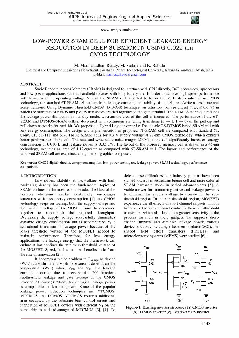
Figure-1. Existing inverter structures (a) CMOS inverter
(b) DTMOS inverter (c) Pseudo-nMOS inverter.
VOL. 13, NO. 4, FEBRUARY 2018 ISSN 1819-6608
ARPN Journal of Engineering and Applied Sciences ©2006-2018 Asian Research Publishing Network (ARPN). All rights reserved.
www.arpnjournals.com
1444
Some of the existing inverter structures along
with their schematics of 1-bit SRAM cells [7], [8] are
shown in Figure-1 and Figure-2. To attain better
performance of the cell, maintain the aspect ratio of the
transistors in the range given by
21W
W
n
p (1)
where Wp and Wn are the widths of the pMOS
and nMOS transistors.
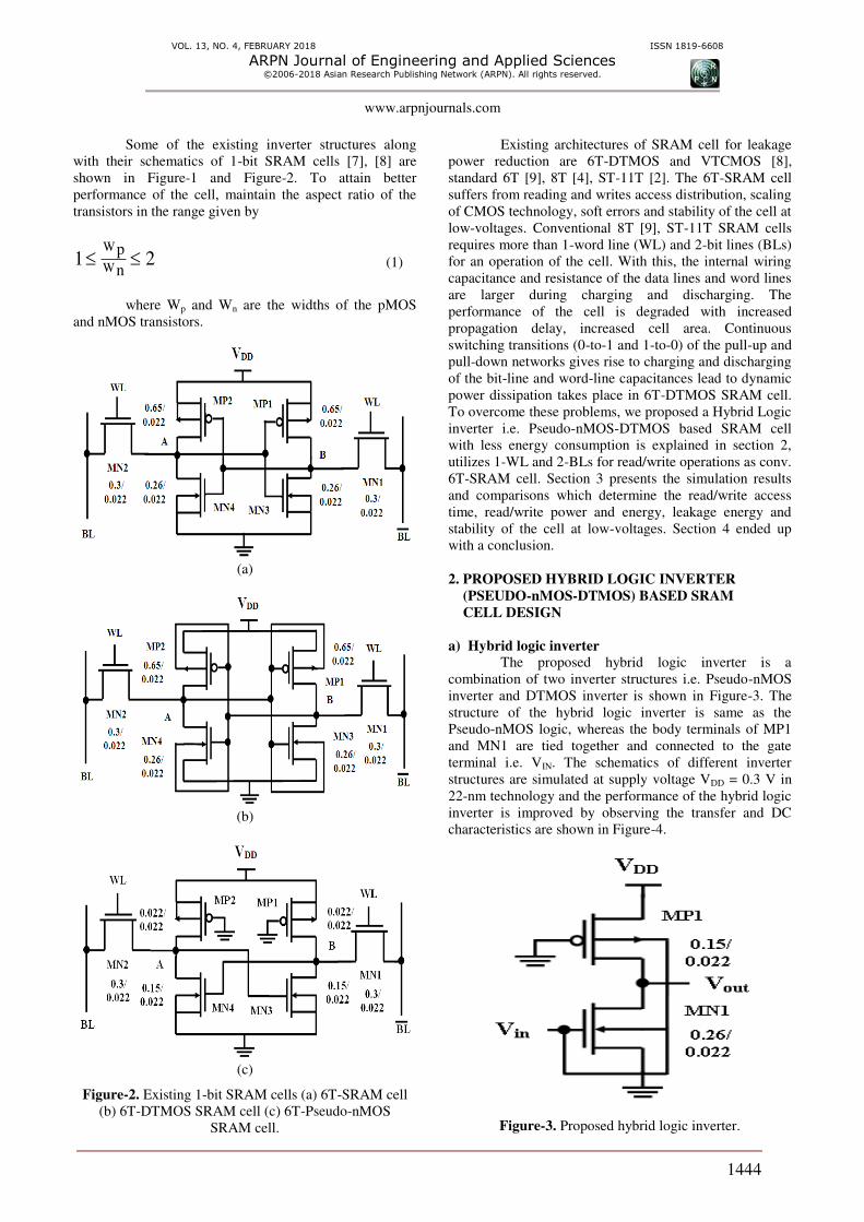
(a)
(b)
(c)
Figure-2. Existing 1-bit SRAM cells (a) 6T-SRAM cell
(b) 6T-DTMOS SRAM cell (c) 6T-Pseudo-nMOS
SRAM cell.
Existing architectures of SRAM cell for leakage
power reduction are 6T-DTMOS and VTCMOS [8],
standard 6T [9], 8T [4], ST-11T [2]. The 6T-SRAM cell
suffers from reading and writes access distribution, scaling
of CMOS technology, soft errors and stability of the cell at
low-voltages. Conventional 8T [9], ST-11T SRAM cells
requires more than 1-word line (WL) and 2-bit lines (BLs)
for an operation of the cell. With this, the internal wiring
capacitance and resistance of the data lines and word lines
are larger during charging and discharging. The
performance of the cell is degraded with increased
propagation delay, increased cell area. Continuous
switching transitions (0-to-1 and 1-to-0) of the pull-up and
pull-down networks gives rise to charging and discharging
of the bit-line and word-line capacitances lead to dynamic
power dissipation takes place in 6T-DTMOS SRAM cell.
To overcome these problems, we proposed a Hybrid Logic
inverter i.e. Pseudo-nMOS-DTMOS based SRAM cell
with less energy consumption is explained in section 2,
utilizes 1-WL and 2-BLs for read/write operations as conv.
6T-SRAM cell. Section 3 presents the simulation results
and comparisons which determine the read/write access
time, read/write power and energy, leakage energy and
stability of the cell at low-voltages. Section 4 ended up
with a conclusion.
2. PROPOSED HYBRID LOGIC INVERTER
(PSEUDO-nMOS-DTMOS) BASED SRAM
CELL DESIGN
a) Hybrid logic inverter
The proposed hybrid logic inverter is a
combination of two inverter structures i.e. Pseudo-nMOS
inverter and DTMOS inverter is shown in Figure-3. The
structure of the hybrid logic inverter is same as the
Pseudo-nMOS logic, whereas the body terminals of MP1
and MN1 are tied together and connected to the gate
terminal i.e. VIN. The schematics of different inverter
structures are simulated at supply voltage VDD = 0.3 V in
22-nm technology and the performance of the hybrid logic
inverter is improved by observing the transfer and DC
characteristics are shown in Figure-4.
Figure-3. Proposed hybrid logic inverter.
VOL. 13, NO. 4, FEBRUARY 2018 ISSN 1819-6608
ARPN Journal of Engineering and Applied Sciences ©2006-2018 Asian Research Publishing Network (ARPN). All rights reserved.
www.arpnjournals.com
1445
(a)
Figure-4. Transfer characteristics.
The threshold voltage VT of the inverter [10] is
given by
k
k21
)VV(k
k2V
V
n
p
pT,DD
n
pnT,
T
(2)
The purpose of a hybrid logic inverter is to
overcome the dynamic power dissipation and leakage
power dissipation with respect to ultra-low VDD at lower
technologies (22-nm). The switching transitions of the
inverter are reduced by pull-up network because of pMOS
transistor. The gate terminal of MP1 is connected to the
ground, so the pMOS transistor is always “ON” [7]. With
this, the load capacitance CL during charging and
discharging of the inverter is reduced which is directly
proportional to the dynamic power.
To operate the proposed inverter at lower VDD,
leakage power is comparable to dynamic power. By
decreasing the VT we can achieve higher performance of
the circuit. Minimization of VT leads to significant
increase in leakage power. For the reduction of leakage
power, the hybrid logic is used as an inverter in the SRAM
memory cell for ultra-low voltage circuits. In this circuit,
the threshold voltage of the device is a function of its gate
voltage, i.e. as the gate voltage increases the threshold
voltage drops resulting in a much higher current drive than
the standard MOSFET for low supply voltages. On the
other hand, VT is high at VGS = 0, therefore the leakage
current is low. The supply voltage of the DTMOS circuit
is restricted by the diode built-in potential. The pn diode
must be reverse biased between the source and the drain.
In order to reduce the leakage power, body terminals of
the inverter are tied together and connected to the gate
terminal [8].
b) 6T-SRAM cell using hybrid logic inverter
Conventionally an SRAM cell is designed by
using two pass transistors and a flip-flop formed by two
cross-coupled inverters. A flip-flop is designed by using
Hybrid Logic inverter requires 6Transistors to build a 1-bit
SRAM cell is shown in Figure-5. In this circuit, MP1,
MN3 and MP2, MN4 form two cross-coupled inverters act
as a flip-flop. MP1, MP2 is the load transistors and MN3,
MN4 are the storage transistors respectively. MN1, MN2
are two access transistors controlled by the word-line
(WL) signal, connected to the complementary bit lines BL
and BL and a flip-flop which acts as a transmission gate
[3].
Figure-5. Schematic diagram of proposed 6T-SRAM cell
using a hybrid logic inverter.
c) Operation of 6T-SRAM cell using hybrid logic
inverter
The read/write operation of the memory cell takes
place by enabling the WL = ‘1’, WL = ‘0’ hold operation
takes place. The complementary bit-lines BL and BL act
as input data lines for the write operation, output data lines
for the read operation. The operation of the memory cell is
as follows: The read/write operation of the cell takes place
whenever the WL = ‘1’ is enabled. The data to be
composed gets exchanged to the BL and its supplement to
the BL .
For example, if data logic ‘0’ is written to the BL,
its complement goes to the BL = ‘1’. A particular memory
cell is selected by enabling the WL = ‘1’; through
transistors MN1 and MN2 the data gets transferred and
write logic ‘0’ at node A and logic ‘1’ is obtained at node
B. The data will remain until it gets altered by other write
operation. The memory cell is selected by enabling the
WL = ‘1’; the read operation takes place. Assume logic’0’ is stored at node A and complement logic ‘1’ at node B.
The current flows from VDD to BL charging through MP1

VOL. 13, NO. 4, FEBRUARY 2018 ISSN 1819-6608
ARPN Journal of Engineering and Applied Sciences ©2006-2018 Asian Research Publishing Network (ARPN). All rights reserved.
www.arpnjournals.com
1446
and MN1. At the same time, BL discharges to the ground
terminal via MN2 and MN4. The stored content is read out
from the memory cell to the output. A small voltage
difference appears at the differential pair of bit-lines where
BL < BL . Whenever the WL = ‘0’ is disabled, the hold
operation takes place [3].
The specifications required for different SRAM
cells [2] are compared as shown in Table-1. Here Diff.-
Differential, SE-Single Ended, BL-Bit line, WL-Word-
Line, RBL-Read bit line, WBL-Word bit line, VGND-
Virtual Ground control for floating node.
Table-1. Comparison of various SRAM cells.
SRAM Cell
Specifications
6T-CMOS
SRAM
Conv.
8T-SRAM
6T-Pseudo-
nMOS SRAM ST-11T
6T- DTMOS
SRAM
Proposed 6T-
Hybrid Logic
SRAM
Writing/Reading Diff./Diff. SE/
Diff. Diff./Diff.
SE/
SE Diff./Diff. Diff./Diff.
Control signals 1-WL 1-WL
1-RWL 1-WL
1-WL
1-RWL
1-VGND
1-WL 1-WL
Bit lines 2-BL 2-WBL
1-RBL 2-BL
1-WBL
1-RBL 2-BL 2-BL
Area (µm2) 1.05 1.44 1.105 2.02 1.397 1.312
3. SIMULATION RESULTS AND COMPARISONS
OF THE CELL
a. Performance of the cell with respect to VDD The proposed SRAM cell using hybrid logic
inverter and the standard 6T, 6T-DTMOS SRAM and 6T-
Pseudo-nMOS SRAM cells are simulated using mentor
graphics at 22-nm technology varying supply voltage VDD
from 0.3-0.5 V. The simulated typical timing waveforms
using different inverter structures of 1-bit SRAM cell is
shown in Figure-6. It denotes x-axis as time (nano-sec)
and y-axis as voltage (volts). BL and BL are two
differential pair of data lines used as input and output
signals for write and read operations. The WL is the
control signal, whereas V (A) and V (B) represent the
output node voltage (each one complement to other) of the
flip-flop. With deep submicron technology, degradation of
output voltage step logic levels i.e. V (A) and V (B) takes
place in 6T-CMOS and 6T-DTMOS. The read access time
TRA and write access time TWA of the cell is increased w.r.t
supply voltage as explained in section 3(iii) and 3(iv).
Figure-6. Stimulated timing waveform of the 1-bit SRAM
cell using different inverter structures at VDD = 0.3 V.
The performance of the memory cell mainly
depends on the two factors. First one is the internal wiring
capacitance and resistance of the data and word lines. The
second one is the continuous switching transitions of the
two cross-coupled inverters from VDD to the ground takes
place in the cell. With this charging and discharging of the
capacitance leads to dynamic power dissipation and delay
of the cell is increased given by
VVL
WCμ
VC2τ
thDD2
ox
DDLdelay
(3)
VOL. 13, NO. 4, FEBRUARY 2018 ISSN 1819-6608
ARPN Journal of Engineering and Applied Sciences ©2006-2018 Asian Research Publishing Network (ARPN). All rights reserved.
www.arpnjournals.com
1447
where CL represents the load capacitance, VDD is
the supply voltage, µ denotes the electron mobility, Cox is
the oxide capacitance, VT is the threshold voltage and W/L
denotes the width to length ratio of the MOSFETs [3]. The
performance of the cell is improved without any loss of
information (data) in terms of output voltage levels using
hybrid logic inverter based 6T-SRAM cell. The different
SRAM cells are simulated at various supply voltages
range from 0.3-1 V. Because of using ultra-low voltage
circuits i.e. VDD ≤ 0.6 V, the performance of the cells are plotted in graphs between 0.3-0.5 V. The minimum VDD
required for operating the 1-bit SRAM cell is shown in
Table-2.
Table-2. Minimum VDD of different SRAM cells.
6T Conv
.8T
ST-
11T
6T-
DTMOS
6T-
Pseudo
-nMOS
6T-
Hybrid
Logic
0.33 0.33 0.36 0.20 0.30 0.26
b. Area comparison
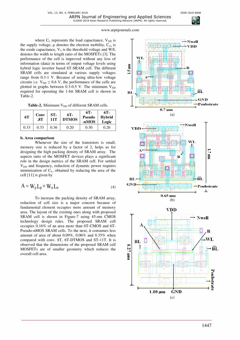
Whenever the size of the transistors is small,
memory size is reduced by a factor of 2, helps us for
designing the high packing density of SRAM array. The
aspects ratio of the MOSFET devices plays a significant
role in the design metrics of the SRAM cell. For settled
VDD and frequency, reduction of dynamic power requires
minimization of CL, obtained by reducing the area of the
cell [11] is given by
LWLWA nnpp (4)
To increase the packing density of SRAM array,
reduction of cell size is a major concern because of
fundamental element occupies more amount of memory
area. The layout of the existing ones along with proposed
SRAM cell is shown in Figure-7 using 45-nm CMOS
technology design rules. The proposed SRAM cell
occupies 0.16% of an area more than 6T-CMOS and 6T-
Pseudo-nMOS SRAM cells. To the next, it consumes less
amount of area of about 0.09%, 0.06% and 0.35% when
compared with conv. 8T, 6T-DTMOS and ST-11T. It is
observed that the dimensions of the proposed SRAM cell
MOSFETs are of smaller geometry which reduces the
overall cell area.
(a)
(b)
(c)

VOL. 13, NO. 4, FEBRUARY 2018 ISSN 1819-6608
ARPN Journal of Engineering and Applied Sciences ©2006-2018 Asian Research Publishing Network (ARPN). All rights reserved.
www.arpnjournals.com
1448
(d)
Figure-7. Layout of (a) 6T-CMOS (b) 6T-Pseudo-nMOS
(c) 6T-DTMOS (d) proposed 6T-hybrid logic SRAM cell.
c. Read access time (TRA) and stability
(a)
(b)
Figure-8. (a) Read access time (TRA) (b) Comparison of
read static noise margin (RSNM) of various SRAM cells.
The TRA is defined as the time duration from the
point when WL is activated to which a 50-mV difference
is built across the complementary bit-lines BL & BLB [2].
The Figure-8(a) represents the comparison of TRA of
various SRAM cells. In the read operation, the Conv. 8T
and ST-11T are associated with higher BL capacitance
(CBL) and having more than 2 BLs resulting higher TRA.
Even though having smaller CBL and 2 BLs for 6T and 6T-
DTMOS, the TRA is higher than the proposed SRAM cells
because of continuous switching of transitions takes place
between VDD to ground in read path.
The read stability of the memory cell at low-
voltages is determined in terms of static noise margin
(SNM). The read SNM (RSNM) of an SRAM cell depends
on the transistor width modulation. The stability of the
SRAM cell depends on the cell ratio and pull-up ratio. Cell
ratio is defined as the ratio between the widths of the pull-
down transistor to the width of the access transistor. The
cell ratio increases, RSNM increases resulting in increased
stability of the cell. This leads to increase in an area of the
cell. To keep the cell area within the reasonable value, the
widths of the cell ratio are in the range given by equation
(1). The stability of the write SNM depends on the pull-up
ratio. It is defined as the ratio of the width of the pull-up
transistor to the width of the access transistor. If pull-up
ratio is increased, the driving capability of the data bit to
be written (or) flip the state of the cell is difficult. By
varying the supply voltage from 0.3 to 0.5V, RSNM is
measured using the method suggested [12], [13] in for
various SRAM cells are shown in Figure-8(b). Compare to
the conv. 8T and ST-11T, the proposed SRAM cell is
having sufficiently greater RSNM.

VOL. 13, NO. 4, FEBRUARY 2018 ISSN 1819-6608
ARPN Journal of Engineering and Applied Sciences ©2006-2018 Asian Research Publishing Network (ARPN). All rights reserved.
www.arpnjournals.com
1449
d. Write access time (TWA) and ability The write-access time (TWA) is defined as the
time duration from the point when WL is activated to
which the storage node (to start with a low level) reaches
to 90% of VDD value for writing logic ‘1’. In the same
way, for writing logic’0’ TWA is defined as the time
duration from the point when WL is activated to which the
storage node (to start with a high level) reaches to 10% of
VDD value [14]. The Figure-9 shows the TWA at various
supply voltages of SRAM cells. Due to single-ended write
operation takes place in ST-11T, a very high TWA for write
‘1’ outlines, whereas other cells are using differential-pair
of bit-lines for writing.
(a)
(b)
Figure-9. Write access time (TWA) at various supply
voltages of SRAM cells (a) Write 0 (b) Write 1.
The TWA of the proposed SRAM cell is lower
than the 6T, Conv. 8T and ST-11T. Because of reduced
critical path for writing the data into the cell by
minimizing the switching transitions of the pull-up and
pull-down networks, in which the delay time or TWA is
directly proportional to the CL. In a transient analysis, the
noise transient signal is applied to the cell which gives
RMS noise of the complementary bit lines is measured
using the simulation method suggested in [15]. The
Figure-10 represents the write RMS Noise Transient at
various supply voltages of SRAM cells.
(a)
Figure-10. Write RMS noise transient at various supply
voltages of SRAM cells, write 0
e. Read/write power and energy consumption The power dissipation is directly proportional to
the supply voltage and load capacitance. Delay is reduced
by increasing the supply voltage and width of the
transistor. This leads to increase of area and power
dissipation of the cell. Therefore for better performance of
the cell, minimize switching transitions and scale down the
technology by maintaining relevant supply voltage and
width of the transistor. The maximum read/write power
and energy consumed by 6T, Conv. 8T, ST-11T and 6T-
DTMOS due to continuous switching of the transitions
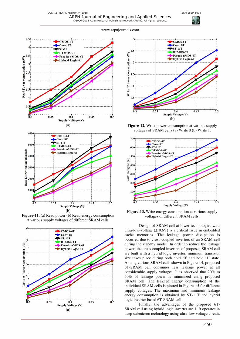
and having higher CBL. The graphs are shown in Figure-
11, Figure-12 and Figure-13 represent that the proposed
SRAM cell consume less read/write power and energy is
observed in the plot due to less CBL of the bit-lines and
load capacitance CL due to switching of the transistors.
The write energy consumption of different SRAM cells is
obtained by an average of write ‘1’ and write ‘0’ power-
delay products (PDP).
VOL. 13, NO. 4, FEBRUARY 2018 ISSN 1819-6608
ARPN Journal of Engineering and Applied Sciences ©2006-2018 Asian Research Publishing Network (ARPN). All rights reserved.
www.arpnjournals.com
1450
(a)
(b)
Figure-11. (a) Read power (b) Read energy consumption
at various supply voltages of different SRAM cells.
(a)
(b)
Figure-12. Write power consumption at various supply
voltages of SRAM cells (a) Write 0 (b) Write 1.
Figure-13. Write energy consumption at various supply
voltages of different SRAM cells.
Design of SRAM cell at lower technologies w.r.t
ultra-low-voltage (≤ 0.6V) is a critical issue in embedded cache memories. The leakage power dissipation is
occurred due to cross-coupled inverters of an SRAM cell
during the standby mode. In order to reduce the leakage
power, the cross-coupled inverters of proposed SRAM cell
are built with a hybrid logic inverter, minimum transistor
size takes place during both hold ‘0’ and hold ‘1’ state.
Among various SRAM cells shown in Figure-14, proposed
6T-SRAM cell consumes less leakage power at all
considerable supply voltages. It is observed that 20% to
50% of leakage power is minimized using proposed
SRAM cell. The leakage energy consumption of the
individual SRAM cells is plotted in Figure-15 for different
supply voltages. The maximum and minimum leakage
energy consumption is obtained by ST-11T and hybrid
logic inverter based 6T-SRAM cell.
Finally, the advantages of the proposed 6T-
SRAM cell using hybrid logic inverter are 1. It operates in
deep submicron technology using ultra-low voltage circuit.

VOL. 13, NO. 4, FEBRUARY 2018 ISSN 1819-6608
ARPN Journal of Engineering and Applied Sciences ©2006-2018 Asian Research Publishing Network (ARPN). All rights reserved.
www.arpnjournals.com
1451
2. In order to replace the DRAM for high-speed
applications such as handheld applications and to interface
with CPU, SRAM is applicable and more suitable. 3. The
leakage and dynamic power reduction take place with
minimum VDD and high-packing density w.r.t proposed
SRAM cell. 4. Degradation of output voltage drop occurs
at the nodes of A and B in existing cells is rectified in the
proposed SRAM cell.5. The combination of two inverters
helps us in reducing the dynamic power with reduced
switching transitions w.r.t pseudo-nMOS inverter. 6.
Reduction of leakage power is achieved by ultra-low
voltage circuit in deep submicron technology.
Figure-14. Leakage power consumption at various supply
voltages of different SRAM cells.
Figure-15. Leakage energy consumption of the cell at
various supply voltages of different SRAM cells.
Standard non-volatile memories such as
EEPROM and Flash memory has grown quickly, leads the
semiconductor technology towards high density and low
cost. Some of the limitations of flash memory are
endurance (limited number of cycles, leads to high cost)
and slow programming speed (limits the applications).
Even though standard volatile memories such as SRAM
and DRAM are having high packing density, requires
battery back-up for information storage whenever the
power is disconnected. To replace the existing non-volatile
(EEPROM and Flash) and volatile (SRAM and DRAM)
memory devices by the advanced non-volatile RAM
technologies (FRAM, PRAM, RRAM, MRAM) with the
ideal characteristics such as non-volatile, reliability,
endurance and high-speed/low-power [16].
CONCLUSIONS
This paper presents a Hybrid Logic inverter based
6T-SRAM cell. The performance of the proposed cell is
significantly improved RSNM and less leakage energy
consumption for applied voltages of considered SRAM
cells. The access time during read/write operations are
minimized, having lower CBL. The power and energy
consumption of the proposed cell is minimized by
reducing the switching transitions of the pull-up and pull-
down networks. With the help of minimum size of cross-
coupled inverters using hybrid logic takes place in the
proposed cell, the leakage power is reduced to 20% to
50%. Finally, for implementation of high performance,
low-power and high-density SRAM architectures for
mobile and storage applications; the essential benefits of
the proposed SRAM cell structures could be fully
exploited.
REFERENCES
[1] Yang Younghwi, et al. 2016. Single Bit-Line 7T
SRAM Cell for Near-Threshold Voltage Operation
With Enhanced Performance and Energy in 14 nm
FinFET Technology. IEEE Transactions on Circuits
and Systems-I: Regular Papers. 63(7): 1023-1032.
DOI: 10.1109/TCSI.2016.2556118.
[2] Ahmad, Sayeed, et al. 2016. Single-Ended Schmitt-
Trigger-Based Robust Low-Power SRAM Cell. IEEE
Transactions on Very Large Scale Integration (VLSI)
Systems. 24(8): 2634-2642.
DOI: 10.1109/TVLSI.2016.2520490.
[3] Kiat-Seng Yeo and Kaushik Roy. 2009. Low voltage,
low power VLSI subsystems. 1st ed., McGraw-Hill,
Inc., New York. ISBN: 9780070677500.
[4] M. Geetha Priya, Dr. K. Baskaran and D.
Krishnaveni. 2011. Leakage Power Reduction
Techniques in Deep Submicron Technologies.
International Conference on Communication
Technology and System Design. Published by

VOL. 13, NO. 4, FEBRUARY 2018 ISSN 1819-6608
ARPN Journal of Engineering and Applied Sciences ©2006-2018 Asian Research Publishing Network (ARPN). All rights reserved.
www.arpnjournals.com
1452
Elsevier Ltd, pp. 1163-1170.
DOI:10.1016/j.proeng.2012.01.976.
[5] Joshi Rajiv V., Rouwaida Kanj and Vinod Ramadurai.
2011. A novel column-decoupled 8T cell for low-
power differential and domino-based SRAM design.
IEEE Transactions on Very Large Scale Integration
(VLSI) Systems. 19(5): 869-882.
DOI: 10.1109/TVLSI.2010.2042086.
[6] Pasandi, Ghasem and Sied Mehdi Fakhraie. 2014. An
8T low-voltage and low-leakage half-selection
disturb-free SRAM using bulk-CMOS and FinFETs.
IEEE Transactions on Electron Devices. 61(7): 2357-
2363. DOI: 10.1109/TED.2014.2321295.
[7] Das Debaprasad. 2010. VLSI design. 1st ed., New
Delhi (India): 1 Jai Singh Road, Oxford University
Press. ISBN: 9780198067665.
[8] Assaderaghi Fariborz, et al. 1997. Dynamic threshold-
voltage MOSFET (DTMOS) for ultra-low voltage
VLSI. IEEE Transactions on Electron Devices. 44(3):
414-422. DOI: 10.1109/16.556151.
[9] Lien, Nan-Chun, et al. A 40 nm 512 kb cross-point 8
T pipeline SRAM with binary word-line boosting
control, ripple bit-line and adaptive data-aware write-
assist. IEEE Transactions on Circuits and Systems I:
Regular Papers. 61(12): 3416-3425.
DOI: 10.1109/TCSI.2014.2336531.
[10] Kang, Sung-Mo and Yusuf Leblebici. 2003. CMOS
digital integrated circuits. 3rd
ed., Tata McGraw-Hill
Education, New York. ISBN: 9780070530775.
[11] Eshraghian, Kamran, Douglas A. Pucknell and Sholeh
Eshraghian. 2005. Essentials of VLSI circuits and
systems. Prentice-Hall of India. ISBN:
9788120327726.
[12] Grossar Evelyn, et al. 2006. Read stability and write-
ability analysis of SRAM cells for nanometer
technologies. IEEE Journal of Solid-State Circuits.
41(11): 2577-2588. DOI: 10.1109/JSSC.2006.883344.
[13] Seevinck Evert, Frans J. List and Jan Lohstroh.1987.
Static-noise margin analysis of MOS SRAM cells.
IEEE Journal of solid-state circuits. 22(5): 748-754.
DOI: 10.1109/JSSC.1987.1052809.
[14] Qiu Hao, et al. 2015. Comparison and statistical
analysis of four write stability metrics in bulk CMOS
static random access memory cells. Japanese Journal
of Applied Physics. 54(4S): 1-5. DOI:
10.7567/JJAP.54.04DC09.
[15] Bolcato P., et al. 1993. A new efficient transient noise
analysis technique for simulation of CCD image
sensors or particle detectors. Custom Integrated
Circuits Conference, Proceedings of the IEEE.
DOI: 10.1109/CICC.1993.590717.
[16] Madhusudhan Reddy. M, Sailaja. M and Babulu. K.
2016. A Survey-Advanced Non-Volatile RAM
Technologies and Its Applications for Future Trends.
International Journal of Control Theory and
Applications. 9(Special Issue): 365-377. DOI:
1504787406.
Related Documents