Low Power Design of Integrated Systems Assoc. Prof. Dimitrios Soudris [email protected].
Dec 22, 2015
Welcome message from author
This document is posted to help you gain knowledge. Please leave a comment to let me know what you think about it! Share it to your friends and learn new things together.
Transcript


Technology Directions:SIA Roadmap
Technology Directions:SIA Roadmap
Year 1999 2002 2005 2008 2011 2014Feature size (nm) 180 130 100 70 50 35
Logic trans/cm2 6.2M 18M 39M 84M 180M 390MCost/trans (mc) 1.735 .580 .255 .110 .049 .022
#pads/chip 1867 2553 3492 4776 6532 8935Clock (MHz) 1250 2100 3500 6000 10000 16900
Chip size (mm2) 340 430 520 620 750 900Wiring levels 6-7 7 7-8 8-9 9 10
Power supply (V) 1.8 1.5 1.2 0.9 0.6 0.5High-perf pow (W) 90 130 160 170 175 183
Battery pow (W) 1.4 2 2.4 2.8 3.2 3.7

Technology Process EvolutionTechnology Directions:
SIA Roadmap 2002Technology Directions:
SIA Roadmap 2002

Transistors#Transistors
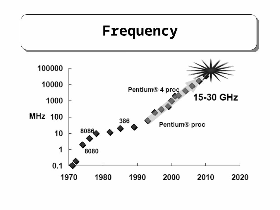
Frequency
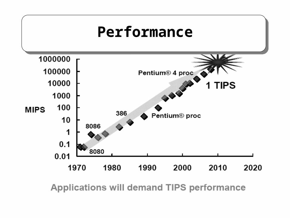
PerformancePerformance

Power ConsumptionPower consumption


Power Terminology
• Power is the rate at which energy is delivered or exchanged» electrical energy is converted to heat energy
during operation
• Power Dissipation - rate at which energy is taken from the source (Vdd ) and converted into heat
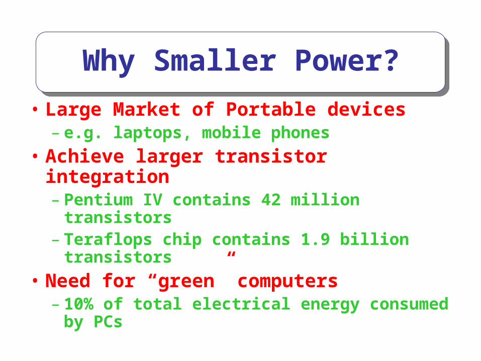
Why Smaller Power?
• Large Market of Portable devices– e.g. laptops, mobile phones
• Achieve larger transistor integration– Pentium IV contains 42 million transistors– Teraflops chip contains 1.9 billion
transistors
• Need for “green” computers– 10% of total electrical energy consumed by
PCs

Battery Technology Improvements
Battery Technology Improvements

The Industry’s Reaction
• Reduce chip capacitance through process scaling
==> Expensive
• Reduce Voltage levels from 5V ί� 3.3V ί�2V
==> Industry is hard to move (microprocessors, memory,...)
• Better Circuit Techniques
==> Gated clocks, Power-Down of non-operational units…
• Example: IBM 80 MHz PowerPC RISC (3 W @ 3.3V)–Power Management Logic determines activity on per cycle basis
–Clocks of idle blocks are turned off ί� 12-30% savings
–Doze - Nap and Sleep mode (5 mW)

Example: Intel Pentium-II processor
• Pentium-1: 15 Watt (5V - 66MHz)• Pentium-2: 8 Watt (3.3V- 133 MHz)

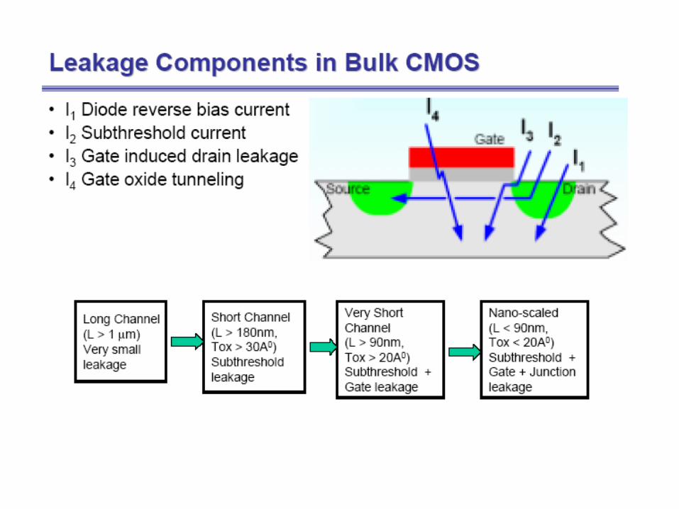
Where Does Power Go in CMOS?
• The power consumption in digital CMOS circuits Pavg = Pdynamic + Pshort-circuit + Pleakage
• Dynamic Power Consumption
• Short Circuit Currents
• Leakage (Static)
Charging and Discharging Capacitors
Short Circuit Path between Supply Rails during Switching
Leaking diodes and transistors

Present & Future in Power Consumption

Dynamic Power Consumption(1)
• where VDD supply voltage, CL capacitance, N is the average number of transitions per clock cycle, and f frequency operation
OUT
C L
Chargingcurrent
OUT
C LDischarging
current
(b) (c)
IN OUT
C L
(a)
V dd V dd V dd
P C V N fdynamic L dd 2

• For technologies up to 0.35 m, the dynamic consumption is about 80% of the total consumption
• Goal ===> reduce dynamic power consumption– reduction capacitance– reduction of supply voltage– reduction of frequency– reduction of switching activity– or combination of above factors
Dynamic Power Consumption (2)

Leakage current consumption
• the reverse-bias diode leakage at the transistor drains and
• the sub-threshold current through an turned-off transistor channel
p+ p+
n-type substrate
+V dd
leakagecurrent
reversed-biased diode(drain-substrate)
gate
The leakage of a reverse-biased pMOS transistor.0.5 1 1.5 20
10 -1510 -13
10 -9
10 -11
10 -7
10 -3
10 -5
Subthresholdregion
Saturatedregion
Decreasing V DS , V dd
Log I D
V GS , volts
Subthreshold leakage with respect to gate-sourcevoltage
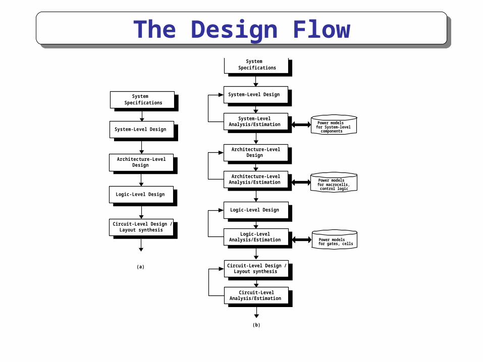
The Design Flow
SystemSpecifications
System-Level Design
Architecture-LevelDesign
Logic-Level Design
Circuit-Level Design /Layout synthesis
SystemSpecifications
System-Level Design
System-LevelAnalysis/Estimation
Architecture-LevelDesign
Architecture-LevelAnalysis/Estimation
Logic-Level Design
Logic-LevelAnalysis/Estimation
Circuit-Level Design /Layout synthesis
Circuit-LevelAnalysis/Estimation
Power modelsfor System-level
components
Power modelsfor macrocells,
control logic
Power modelsfor gates, cells
(a)
(b)
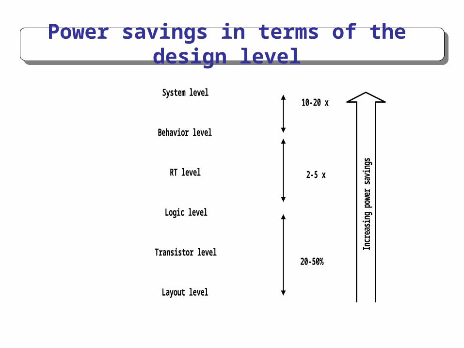
Power savings in terms of the design level
System level
Behavior level
Logic level
Transistor level
Layout level
RT level
10-20 x
2-5 x
20-50%
Incr
easin
g po
wer s
avin
gs
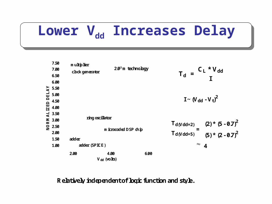
Lower Vdd Increases Delay
CL * Vdd
I=Td
Td(Vdd=5)
Td(Vdd=2)=
(2) * (5 - 0.7)2
(5) * (2 - 0.7)2
4
I ~ (Vdd - Vt)2
Relatively independent of logic function and style.
1.00
1.50
2.00
2.50
3.00
3.50
4.00
4.50
5.00
5.50
6.00
6.50
7.00
7.50
2.00 4.00 6.00Vdd (volts)
NO
RM
AL
IZE
D D
EL
AY
adder (SPICE)
microcoded DSP chip
multiplier
adder
ring oscillator
clock generator2.0m technology

P x td = Et = CL * Vdd2
E(Vdd=2)=
(CL) * (2)2
(CL) * (5)2E(Vdd=5)
Strong function of voltage (V2 dependence).
Relatively independent of logic function and style.
E(Vdd=2) 0.16 E(Vdd =5)
0.03
0.05
0.07
0.1
0.15
0.20
0.30
0.50
0.70
1.00
1.5
1 2 5
51 stage ring oscillator
8-bit adder
Vdd (volts)
quadratic dependence
NO
RM
AL
IZE
D P
OW
ER
-DE
LA
Y P
RO
DU
CT
Power Delay Product Improves with lowering VDD.
Reducing VddReducing Vdd

Lowering the Threshold
DESIGN FOR PLeakage == PDynamic
Vt = 0.2Vt = 0
ID
VGS
Reduces the Speed Loss, But Increases Leakage
Vdd
Delay
2Vt
Interesting Design Approach:

Transistor Sizing for Power Minimization
Minimum sized devices are usually optimal for low-power.
Small W/L’s
Large W/L’s
Higher Voltage
Lower Voltage
Lower Capacitance
Higher Capacitance
Larger sized devices are useful only when interconnect dominated.

Techniques to reduce supply voltage
Algorithm
Architecture
Circuit/Logic
Technology
Transformation to exploitconcurrency
Parallelism and Pipelining
Transistor Sizing, Fast LogicStructures
Threshold Voltage Reduction,Feature Size scaling

Techniques to minimizing the switched capacitance
Partitioning, Power-down, power states
Complexity, Concurrency, Regularity,Locality, Data representation
Concurrency, Instruction set selection,Signal correlations,
Data representation, Data Encoding
Transistor sizing, Logic optimization,Power down, Layout Optimization
Advanced packaging, SOI
Architecture
Circuit/Logic
Technology
Algorithm
USystem
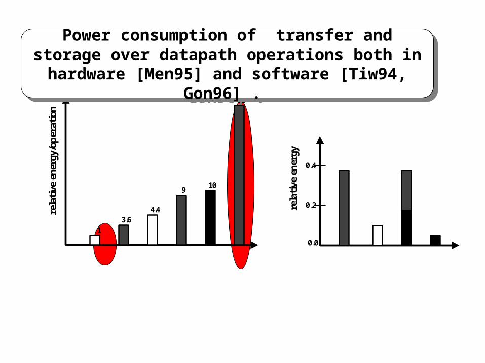
13.6
4.4
910
33
rela
tive
en
ergy
/op
erat
ion
rela
tive
en
ergy
0.0
0.2
0.4
Power consumption of transfer and storage over datapath operations both in hardware [Men95] and software [Tiw94,
Gon96] .
Power consumption of transfer and storage over datapath operations both in hardware [Men95] and software [Tiw94,
Gon96] .

Architecture Power Optimization Techniques
•Architecture-driven voltage reduction: The key idea is to speed up the circuit in order to be able reduces voltage while meeting throughput rate constraints. Voltage reduction can be achieved by introducing parallelism in hardware or inserting flip-flops
•Switching activity minimization: Try to prevent the generation and propagation of spurious transitions or to reduce the number of transitions, e.g. retiming, path balancing, data representation
•Switched capacitance minimization: Aim at the minimization of switched capacitance
•Dynamic power management: Under certain conditions, a circuit part becomes inactive, avoiding unnecessary calculations, e.g. gated clocks, operand isolation, pre-computation, and guarded evaluation

Architecture Trade-offs: Reference Data Path
• Critical path delay Tadder + Tcomparator (= 25ns), fref = 40MHz
• Total capacitance being switched = Cref
• Vdd = Vref = 5V
• Power for reference datapath = Pref = Cref Vref2 fref

Voltage Reduction Technique: Parallelism
• The clock rate can be reduced by half with the same throughput
fpar = fref / 2
• Vpar = Vref / 1.7 Cpar = 2.15 Cref
• Ppar = (2.15 Cref ) (Vref /1.7)2 (fref /2) 0.36 P ref

Voltage Reduction Technique: Pipeline
• fpipe = fref, Cpipe = 1.1 Cref, Vpipe = Vref /1.7
• Voltage can be dropped while maintaining the original throughput
• Ppipe = Cpipe Vpipe2 fpipe = (1.1 Cref ) (Vref /1.7)2 fref = 0.37 Pref

Comparisons

Logic Style and Power Consumption
• Power-delay product improves as voltage decreases• The “best” logic style minimizes power-delay for a given delay constraint

The concept of gating clock signals
0 1
R E G clo ck
X Y
B
A <
<
c lo ck
g a tedc lo ck
sch em e 1
<
c lo ck
g a tedc lo ck
sch em e 2
co m p a ra to ro u tp u t
g a ted c lo ck(sch em e 2 )
g a ted c lo ck(sch em e 1 )
c lo ck
0
0
0
0
1 c lo ck p er io d
(a ) (c )(b )

Resource Sharing Can Increase Activity

Global bus architecture Local bus architecture
Shared Resources incur Switching Overhead
Reducing Effective CapacitanceReducing Effective Capacitance

Data representation
• Sign-extension activity significantly reduced using sign-magnitude representation
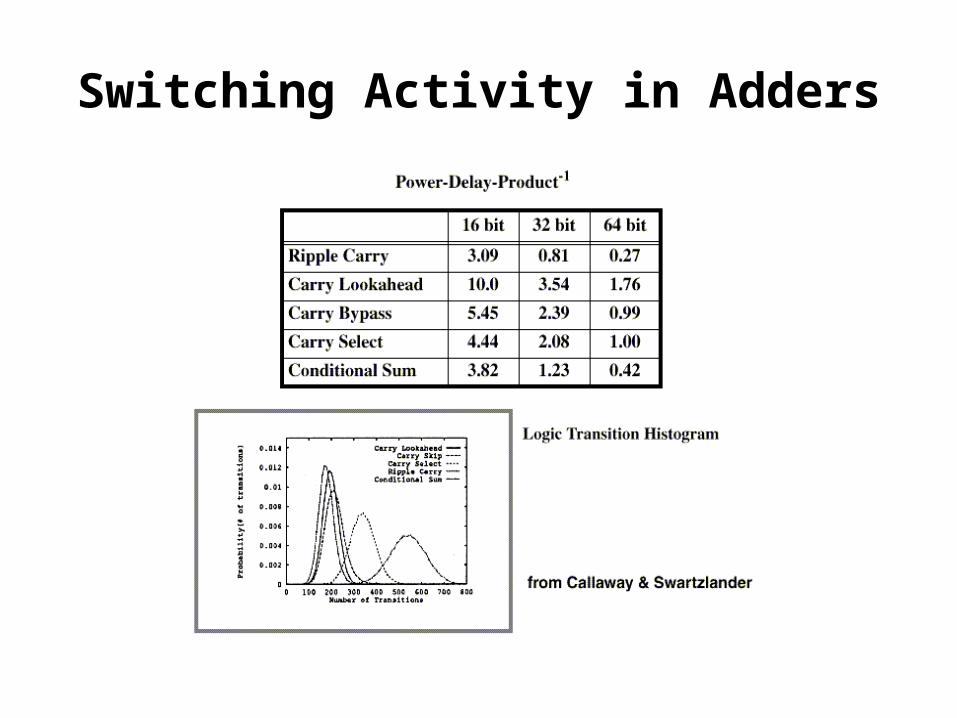
Switching Activity in Adders

Switching Activity in Multipliers

Signals and Operations Reordering
• Example: complex multiplication
Trading a multiplication for an addition
(a) (b)
x
X r
x
-
X i
A rA i
Y r
x
X r
x
+
X i
A iA r
Y i
A i-A r x
X r
x
+
A r
Y i
x
X i
Y r
A i+A r
-
+
X r X i

Module Selection
* **i ii iii
+ i
+ ii
(a)
(c)
(d)
* **i ii iii
+
+ ii
*ii iii
+ i
+ ii
** i
Area =2744
Latency=30 ns
Power=1199μW
rippleadder
carryloohahead
adder
Area =3959
Latency=20 ns
Power=1467μW
arraymultiplier
wallacemultiplier
Area =16185
Latency=60 ns
Power=18540μW
Area =18443
Latency=40 ns
Power=23545μW
RTLLibrary
(b)

Glitching activity reduction (3)
x y
z
ARCHITECTURE 1
Power Consumption:Without glitches: 823.9 μWWith glitches: 1650 μW
ARCHITECTURE 2
Power Consumption:Without glitches: 951.7 μWWith glitches: 1357.7 μW
Functionif (x < y) then z=c+delse z=a+b
a c
0 1
x y
a b c db d
0 1
0 1
z

Two-Level Logic Circuits Switching Activity Minimization (1)
• Taking into account the static and transition probabilities (i.e. temporal correlation) of the primary inputs, we can insert in certain gates of the first logic level (i.e. AND gates), additional input signals resulting into reduced switching activity
• Appropriately-selected input signals force the outputs of the AND gates to logic level zero for a number of combinations of the binary input signals

Two-Level Logic Circuits Switching Activity Minimization (2)
• Example:
• Signal x3 exhibits low-transition probability and high static-1 probability, while the signals x0 , x1, and x2 are characterized by high-transition probabilities
F'g4g4
g 1
g 2
g 3
x 0x 1
x 0x 2
x 0x 3
x 3
'y 1
'y 2
'y 3
Fg4
g 1
g 2
g 3
x 0x 1
x 0x 2
x 0x 3
y 1
y 2
y 3
g 4
Intial Logic Circuit Modified Logic circuit
F x x x x x x 0 1 0 2 0 3

• A. Chandrakasan and R. Brodersen, “Low Power CMOS Design”, Kluwer Academic Publishers, 1995
• Christian Piguet, Editor, « Low-Power Electronics Design”, CRC Press, November 2004
• D. Soudris, C. Piguet, C. Goutis, “Designing CMOS Circuits for Low-Power”, Kluwer Academic Press, October 2002
• F. Catthoor, K. Danckaert, et. al.: 2002, Data Access and Storage Management for Embedded Programmable Processors. Kluwer Academic Publishers
• Stamatis Vassiliadis and Dimitrios Soudris, “Fine- and Coarse-Grain Reconfigurable Computing” Springer, Dordrecht/London/Boston, August 2007
• http://vlsi.ee.duth.gr/~dsoudris• AMDREL website http://vlsi.ee.duh.gr/amdrel
Additional InfoAdditional Info
Related Documents