Application Note R30AN0392EJ0100 Rev.1.00 Page 1 of 39 Oct.12.21 RA2E1 Group Low Power Application (Usage of ADC, DTC and ELC at Snooze mode) for FPB-RA2E1 Introduction This application note describes the features of RA2E1 MCU that are useful for low-power operation, typically required for logging data for long durations. The FPB-RA2E1 kit is used for creating such a low-power data logging system. The functionality demonstrated here is typically required in products such as fitness trackers, fleet tracking devices, and so forth. The data logger uses the 12-bit A/D Converter (ADC), Data Transfer Controller (DTC), Asynchronous General-purpose Timer (AGT), Real-time Clock (RTC), Event Link Controller (ELC), Data Operation Circuit (DOC), and Low-power Mode (LPM). The Snooze mode and Software Standby mode are used to reduce power consumption by minimizing the CPU operation time. Application projects use the Integrated Development Environment e 2 studio IDE and Flexible Software Package (FSP) provided for the RA family. This application note has been changed to a simple function from application note "RA2L1/RA2E1 Group Low Power Application Example (Data Logger)" (R30AN0384) so that operation can be confirmed with FPB- RA2E1 alone. Prerequisites We assume that you have developed Renesas e 2 studio IDE and Flexible Software Package (FSP). We recommend that you build and run the Blinky project according to section “Tutorial: Your First RA MCU Project – Blinky” in FSP User’s Manual (R11UM0155) prior to trying out this application. You can then become familiar with e 2 studio IDE and FSP and verify that the debugging connectivity to the boards is working correctly. Required Resources This application project is created for Renesas RA Family MCU RA2E1. When applying this application note to other MCUs, be sure to change it according to the specifications of the MCU and evaluate it carefully. The resources required for this application project are as follows. Hardware • Renesas RA Kit FPB-RA2E1 • Seeed Grove Base Shield V2.0 for Arduino (www.seeedstudio.com/Base-Shield-V2.html) • Seeed Grove - Luminance Sensor (www.seeedstudio.com/Grove-Luminance-Sensor.html) • Seeed Grove - Temperature Sensor (www.seeedstudio.com/Grove-Temperature-Sensor.html) • USB – TTL Serial connector Development Tools and Software • e 2 studio IDE version 2021-10 (21.10.0) or later • Renesas Flexible Software Package (FSP) version 3.4.0 or later • GCC ARM Embedded Toolchain version 9.3.1.20200408 or later • Terminal software (like Tera Term)

Welcome message from author
This document is posted to help you gain knowledge. Please leave a comment to let me know what you think about it! Share it to your friends and learn new things together.
Transcript

Application Note
R30AN0392EJ0100 Rev.1.00 Page 1 of 39 Oct.12.21
RA2E1 Group Low Power Application (Usage of ADC, DTC and ELC at Snooze mode) for FPB-RA2E1 Introduction This application note describes the features of RA2E1 MCU that are useful for low-power operation, typically required for logging data for long durations. The FPB-RA2E1 kit is used for creating such a low-power data logging system. The functionality demonstrated here is typically required in products such as fitness trackers, fleet tracking devices, and so forth. The data logger uses the 12-bit A/D Converter (ADC), Data Transfer Controller (DTC), Asynchronous General-purpose Timer (AGT), Real-time Clock (RTC), Event Link Controller (ELC), Data Operation Circuit (DOC), and Low-power Mode (LPM). The Snooze mode and Software Standby mode are used to reduce power consumption by minimizing the CPU operation time. Application projects use the Integrated Development Environment e2studio IDE and Flexible Software Package (FSP) provided for the RA family.
This application note has been changed to a simple function from application note "RA2L1/RA2E1 Group Low Power Application Example (Data Logger)" (R30AN0384) so that operation can be confirmed with FPB-RA2E1 alone.
Prerequisites We assume that you have developed Renesas e2studio IDE and Flexible Software Package (FSP). We recommend that you build and run the Blinky project according to section “Tutorial: Your First RA MCU Project – Blinky” in FSP User’s Manual (R11UM0155) prior to trying out this application. You can then become familiar with e2studio IDE and FSP and verify that the debugging connectivity to the boards is working correctly.
Required Resources
This application project is created for Renesas RA Family MCU RA2E1. When applying this application note to other MCUs, be sure to change it according to the specifications of the MCU and evaluate it carefully. The resources required for this application project are as follows.
Hardware
• Renesas RA Kit FPB-RA2E1 • Seeed Grove Base Shield V2.0 for Arduino (www.seeedstudio.com/Base-Shield-V2.html) • Seeed Grove - Luminance Sensor (www.seeedstudio.com/Grove-Luminance-Sensor.html) • Seeed Grove - Temperature Sensor (www.seeedstudio.com/Grove-Temperature-Sensor.html) • USB – TTL Serial connector Development Tools and Software
• e2 studio IDE version 2021-10 (21.10.0) or later • Renesas Flexible Software Package (FSP) version 3.4.0 or later • GCC ARM Embedded Toolchain version 9.3.1.20200408 or later • Terminal software (like Tera Term)

RA2E1 Group Low Power Application (Usage of ADC, DTC and ELC at Snooze mode) for FPB-RA2E1
R30AN0392EJ0100 Rev.1.00 Page 2 of 39 Oct.12.21
Contents
1. Overview ................................................................................................................................. 4 1.1 Overview of Specifications ...................................................................................................................... 4 1.1.1 Data Acquisition Function/Level Judgment Function ............................................................................ 5 1.1.2 Data Output Function ............................................................................................................................ 6 1.2 Peripheral Modules of RA2E1 MCU ........................................................................................................ 7
2. Description of Functions Used ................................................................................................. 8 2.1 Low Power Modes ................................................................................................................................... 8 2.1.1 Available Low Power Modes ................................................................................................................. 8 2.1.2 Low Power Mode Transition Events ...................................................................................................... 9 2.2 12-bit A/D Converter .............................................................................................................................. 10 2.2.1 A/D Conversion Channel ..................................................................................................................... 11 2.2.2 Conversion Start Event ....................................................................................................................... 12 2.2.3 Data Register Automatic Clearing Function ........................................................................................ 12 2.3 DTC Transfer ......................................................................................................................................... 13 2.3.1 Transfer Start Event ............................................................................................................................ 13 2.3.2 Chain Transfer ..................................................................................................................................... 14 2.4 DOC Subtraction Mode ......................................................................................................................... 16 2.5 ELC Event Connection .......................................................................................................................... 18 2.6 Two-channel Connected AGT ............................................................................................................... 19 2.7 RTC Mode Selection ............................................................................................................................. 20 2.8 Clock Output .......................................................................................................................................... 20
3. Low-power Data Logger Application ...................................................................................... 21 3.1 Functional Specification ........................................................................................................................ 21 3.1.1 Data Acquisition Function .................................................................................................................... 21 3.1.2 Data Level Judgement Function.......................................................................................................... 21 3.1.3 Data Output Function .......................................................................................................................... 21 3.2 User Interface ........................................................................................................................................ 22 3.2.1 Connect the Sensor ............................................................................................................................. 23 3.2.2 Connect the USB-TTL Connector ....................................................................................................... 24 3.2.3 Data Communication Specifications ................................................................................................... 24 3.2.3.1 Communication Data Format ............................................................................................................ 24 3.2.4 Input/Output Pins for Debugging ......................................................................................................... 25 3.3 Clock Input ............................................................................................................................................. 26 3.4 Debugging ............................................................................................................................................. 27 3.4.1 Canceling the Low Power Mode by Pressing Down the User Switch ................................................. 27 3.4.2 Checking the Low Power Mode Status ............................................................................................... 27 3.5 Flowchart ............................................................................................................................................... 29
4. Evaluating Applications .......................................................................................................... 34

RA2E1 Group Low Power Application (Usage of ADC, DTC and ELC at Snooze mode) for FPB-RA2E1
R30AN0392EJ0100 Rev.1.00 Page 3 of 39 Oct.12.21
4.1 Import and Building a Project ................................................................................................................ 34 4.2 Download and Debug a Project ............................................................................................................. 34 4.3 Procedure for Checking the Operation of the Low-power Data Logger ................................................ 35 4.4 Evaluating the Current Consumption .................................................................................................... 36 4.5 Notes on Free-run Operation with the FPB-RA2E1 Kit ......................................................................... 37
5. References ............................................................................................................................ 37
Revision History ............................................................................................................................ 39

RA2E1 Group Low Power Application (Usage of ADC, DTC and ELC at Snooze mode) for FPB-RA2E1
R30AN0392EJ0100 Rev.1.00 Page 4 of 39 Oct.12.21
1. Overview 1.1 Overview of Specifications This application project acquires sensor data and compares it against thresholds at regular intervals. These processes are intermittently executed with Snooze mode during Software Standby mode to achieve operation as a low-power data logger.
In this application project, Snooze mode is entered every 30 minutes during Software Standby mode. While operating in Snooze mode, A/D conversion and the level judgment of the result are performed. After judging the level, the system returns to the Software Standby mode. However, if the conversion result is greater than or equal to the threshold value, Snooze mode is canceled and MCU is transitioned to Normal mode. In addition, the low power mode is canceled every 24 hours, and the measured data accumulated in the buffer is transmitted. After the data transmission, the process repeats. When a user button is pressed, the low power mode is canceled, and the requested data is transmitted. Table 1 explains the details of these processes for each function.
Table 1. List of Functions
Function Process Description Data Acquisition Function A/D conversion is triggered by AGT count underflow event, and conversion
result are stored in the measurement data buffer. Level Judgement Function The level of A/D conversion results is judged by the Data Operation Circuit
(DOC). If the conversion result is greater than or equal to the threshold value, the interrupt is occurred.
Data Output Function When the RTC alarm interrupt, external IRQ interrupt and DOC interrupt occur, the mode shifts to Normal mode and the data is output by UART communication.
Figure 1 shows the MCU states and mode transition events, and Figure 2 shows a conceptual diagram of the operation modes and current consumption.
Figure 1. MCU Status and Mode Transition Events

RA2E1 Group Low Power Application (Usage of ADC, DTC and ELC at Snooze mode) for FPB-RA2E1
R30AN0392EJ0100 Rev.1.00 Page 5 of 39 Oct.12.21
Note: The current consumption and the duration of each process are conceptual.
Figure 2. Conceptual Diagram of Operation Mode and Current Consumption
1.1.1 Data Acquisition Function/Level Judgment Function In the data acquisition function, the AGT timer interrupt transitions from Software Standby mode to Snooze mode and performs A/D conversion on two channels. The A/D conversion result is stored in the measurement data buffer using the DTC. By DTC transfer completion event, the system returns to Software Standby mode.
The level judgement function judges the level of A/D conversion results by the Data Operation Circuit (DOC). If the conversion result is greater than or equal to the threshold value, the DOC interrupt is occurred and MCU is transitioned to Normal mode.
The processing sequence for the above functions is described using Figure 3. Figure 1.3.
① AGT0 timer generates an AGT0 underflow signal at every 1 minute.
② AGT1 timer uses the AGT0 underflow signal as the count source and creates and AGT1 underflow interrupt at 30 counts (every 30 minutes) of this signal. When AGT1 underflow interrupt occurs, it requests a transition to Snooze mode.
③ The ADC starts A/D conversion by a synchronous trigger from the ELC linked event from AGT1 or Snooze request event.
④ When an ADC conversion end interrupt is generated, the DTC performs transfer processing in the following order according to the transfer information set for repeat transfer mode and chain transfer.
a. The conversion result of A/D converter channel 0 is transferred to the channel 0 measurement data buffer.
b. The conversion result of A/D converter channel 1 is transferred to the channel 1 measurement data buffer.
c. The value of the level judgment threshold storage variable is transferred to the DOC data setting register.
d. The conversion result of A/D converter channel 1 is transferred to the DOC data input register.
⑤ When the level judgment result event (Data Operation Circuit interrupt) of channel 1 is occurred, the Snooze mode is canceled.
⑥ When a Not DTC transfer completion interrupt (DTC_TRANSFER) is generated due to completion of the transfer processing of ④, the system returns to the Software Standby mode.

RA2E1 Group Low Power Application (Usage of ADC, DTC and ELC at Snooze mode) for FPB-RA2E1
R30AN0392EJ0100 Rev.1.00 Page 6 of 39 Oct.12.21
Note: The duration of each processing and event occurrence represents a concept. Note: The processing sequence ① is omitted. Refer to section 2.6 Two-channel Cconnected AGT for details.
Figure 3. Timing Chart for Data Acquisition and Level Judgement
1.1.2 Data Output Function The data output function transitions from Software Standby mode to Normal mode by RTC alarm interrupt, external IRQ interrupt and DOC interrupt, and outputs data by UART communication. After the data output is completed, it transits to low power mode. However, if the transition request event to Normal mode is RTC alarm interrupt, the RTC alarm for the next transition from Software Standby mode to Normal mode is set, and then the mode transitions to the low power mode.

RA2E1 Group Low Power Application (Usage of ADC, DTC and ELC at Snooze mode) for FPB-RA2E1
R30AN0392EJ0100 Rev.1.00 Page 7 of 39 Oct.12.21
The above functions are described in the processing sequence as follows:
① When RTC alarm interrupt, external IRQ interrupt and DOC interrupt are occurred, it cancels the low power mode.
② After the low power mode is canceled, transmit data is generated and the SCI outputs the data.
③ Transits to low power mode after the data output is completed. 1.2 Peripheral Modules of RA2E1 MCU Table 2 lists the main peripheral modules of RA2E1 MCU used in this application project and their typical uses. These are illustrated in the functional overview of RA2E1 MCU in Figure 4.
Table 2. Main Peripheral Modules
Module Typical Uses Low Power Modes The Snooze mode and the Software Standby mode are used to achieve low
power consumption. 12-bit ADC Converts the analog continuous time signal from the sensor to discrete digital
signal value. DTC The analog conversion result of the A/D converter is transferred to the buffer using
the DTC in repeat transfer mode. A DTC chain transfer is used to transfer the data from the ADC data register, and from RAM/ROM memory to the DOC register for level judgement.
DOC Use the subtraction mode to judge the level of the A/D conversion result. 16-bit AGT 0/1 Generates a transition request to Snooze mode and start data acquisition timing
every 30 minutes. RTC Measure the time since power on. The 24-hour alarm interrupt is used to cancel
the low power mode and generate the timing of data output. SCI Performs UART communication with the external equipment. ELC Connect a Snooze transition request event or an AGT underflow event to the A/D
converter start conversion event.

RA2E1 Group Low Power Application (Usage of ADC, DTC and ELC at Snooze mode) for FPB-RA2E1
R30AN0392EJ0100 Rev.1.00 Page 8 of 39 Oct.12.21
Figure 4. Outline of RA2E1 MCU Function
2. Description of Functions Used This section describes the functions of the LPM, ADC, DTC, ELC, AGT, and RTC modules of RA2E1 MCU and explains how to set them to achieve the expected operation.
2.1 Low Power Modes 2.1.1 Available Low Power Modes Table “Operating conditions of each low power mode” in RA2E1 User's Manual (R01UH0852) describes the conditions to transition to low power modes, the states of the CPUs and peripheral modules, and the condition to cancel each mode.
The available low power modes are as follows:
• Sleep mode • Software Standby mode • Snooze mode

RA2E1 Group Low Power Application (Usage of ADC, DTC and ELC at Snooze mode) for FPB-RA2E1
R30AN0392EJ0100 Rev.1.00 Page 9 of 39 Oct.12.21
Figure 5 shows a schematic diagram of the low power mode transitions.
Figure 5. Schematic Diagram of Low Power Mode Transitions (1) Sleep Mode Generally, CPU operation is the most significant factor for the increase in power consumption. In this mode, CPU halts operation but retains the value of CPU's internal registers. Peripheral functions other than CPU are not stopped. The Sleep mode is canceled when an available reset or interrupt occurs in Sleep mode. All interrupt sources are available. When using interrupts to cancel Sleep mode, the corresponding IELSRn register must be set prior to executing WFI instruction.
(2) Software Standby Mode This mode dramatically reduces power consumption by stopping the CPU, most on-chip peripheral functions, and oscillators. However, CPU’s internal registers, SRAM data, the on-chip peripheral functions, and I/O port status are retained.
(3) Snooze Mode This mode is an extension of Software Standby mode that allows limited peripheral modules to operate with the CPU halted. This reduces current consumption by flexible operation of peripheral modules required by the application. Snooze mode can be entered from Software Standby mode by a specified interrupt request. Interrupt requests available in Snooze mode can also transition from Snooze mode to Normal mode or Software Standby mode.
2.1.2 Low Power Mode Transition Events For details on the available low power mode transitions, refer to the relevant sections in RA2E1 User's Manual (R01UH0852) below.
• Table: Available Snooze requests to switch to Snooze mode. • Table: Available Snooze end requests (triggers to return to Software Standby mode). • Table: Available interrupt sources to transition to Normal mode from Snooze mode and Software Standby
mode. Table 3 lists the mode transition events used in this application project. Figure 2.2Figure 6 also shows the low power transition event settings on FSP configurator.

RA2E1 Group Low Power Application (Usage of ADC, DTC and ELC at Snooze mode) for FPB-RA2E1
R30AN0392EJ0100 Rev.1.00 Page 10 of 39 Oct.12.21
Table 3. Mode Transition Events Used in this Application Project
Transition Request Event Request for transition to Snooze mode AGT_AGTI Snooze mode end request DTC_TRANSFER Request for transition to Normal mode from Snooze mode or Software Standby mode
PORT_IRQ RTC_ALM DOC_DOPCI
Figure 6. Low Power Mode Transition Event Settings on FSP Configurator
2.2 12-bit A/D Converter RA2E1 MCU includes a 12-bit successive approximation A/D converter (ADC12) unit. There are three types of scan conversion operation modes and two types of conversion modes as shown below.
• Single scan mode: Executes the scan of the specified channel once. • Continuous scan mode: Scanning of the specified channels is repeated until ADCSR.ADST bit is set to 0
by software. • Group scan mode: The scan of the channel selected in Groups A and B is executed once by the
synchronous trigger. • High-speed A/D conversion mode1: Executes A/D conversion at high speed. • Low-power A/D conversion mode1: The A/D conversion time is longer than the High-speed conversion
mode, but it executes with low power consumption. Note: Refer to section “Analog Input Sampling and Scan Conversion Time” and Table “Operating and
standby current” in RA2E1 User's Manual (R01UH0852) for deep understanding of deference between A/D conversion modes.
Transition request events from Snooze mode and Software Standby mode to Normal mode
Snooze mode end request events
Transition request events to Snooze mode Transition request events from Snooze mode to Normal mode
RA2E1 Group Low Power Application (Usage of ADC, DTC and ELC at Snooze mode) for FPB-RA2E1
R30AN0392EJ0100 Rev.1.00 Page 11 of 39 Oct.12.21
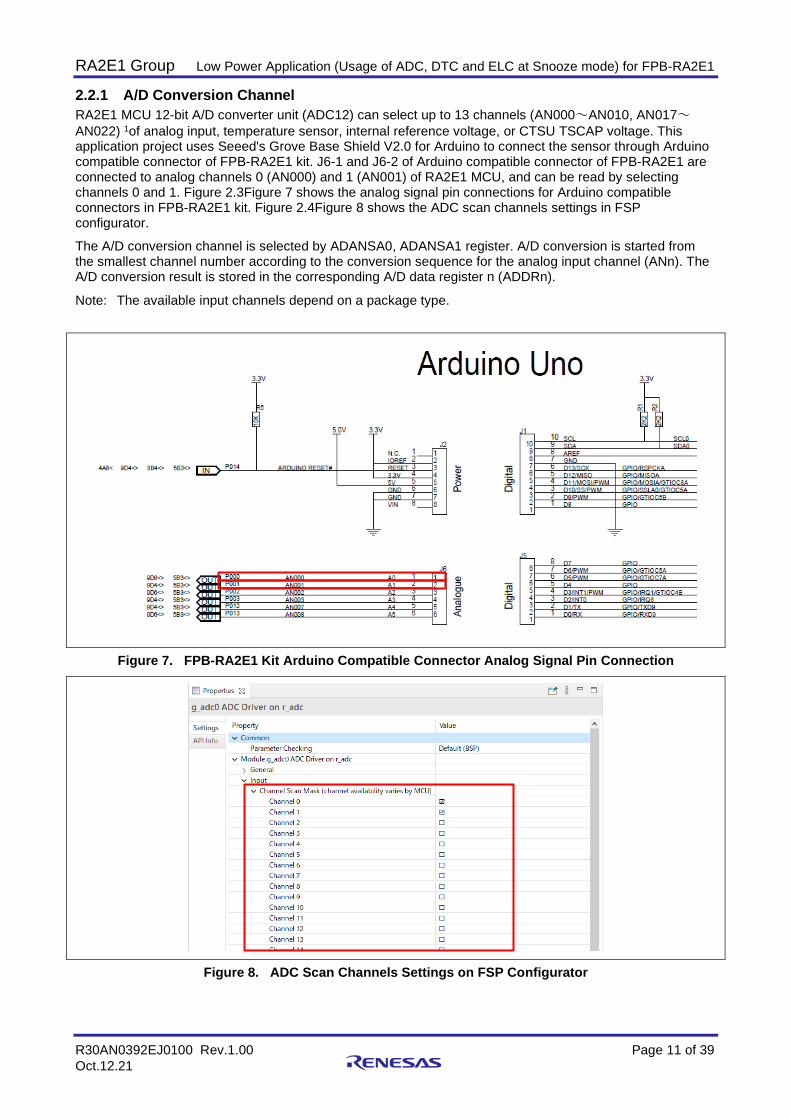
2.2.1 A/D Conversion Channel RA2E1 MCU 12-bit A/D converter unit (ADC12) can select up to 13 channels (AN000~AN010, AN017~AN022) 1of analog input, temperature sensor, internal reference voltage, or CTSU TSCAP voltage. This application project uses Seeed's Grove Base Shield V2.0 for Arduino to connect the sensor through Arduino compatible connector of FPB-RA2E1 kit. J6-1 and J6-2 of Arduino compatible connector of FPB-RA2E1 are connected to analog channels 0 (AN000) and 1 (AN001) of RA2E1 MCU, and can be read by selecting channels 0 and 1. Figure 2.3Figure 7 shows the analog signal pin connections for Arduino compatible connectors in FPB-RA2E1 kit. Figure 2.4Figure 8 shows the ADC scan channels settings in FSP configurator.
The A/D conversion channel is selected by ADANSA0, ADANSA1 register. A/D conversion is started from the smallest channel number according to the conversion sequence for the analog input channel (ANn). The A/D conversion result is stored in the corresponding A/D data register n (ADDRn).
Note: The available input channels depend on a package type.
Figure 7. FPB-RA2E1 Kit Arduino Compatible Connector Analog Signal Pin Connection
Figure 8. ADC Scan Channels Settings on FSP Configurator

RA2E1 Group Low Power Application (Usage of ADC, DTC and ELC at Snooze mode) for FPB-RA2E1
R30AN0392EJ0100 Rev.1.00 Page 12 of 39 Oct.12.21
2.2.2 Conversion Start Event Figure 2.5Figure 9 shows ADC12 Input/Output events. ADC12 conversion start condition can be selected from three triggers: software trigger, synchronous trigger from ELC, and asynchronous trigger by external trigger ADTRG0 pin. In this application project, the synchronous trigger from the ELC is selected as the conversion start condition. Figure 2.6Figure 10 shows the A/D conversion start trigger event settings in FSP configurator.
A/D conversion of a synchronous trigger from the ELC can be started by the preset event of the ELC specified by ELSRn register as shown below. Set ADCSR.TRGE bit to 1 and ADCSR.EXTRG bit to 0, and select the corresponding source in ADSTRGR.TRSA[5:0] and ADSTRGR.TRSB[5:0] bits.
• Select ELC_AD00 in the ELC. ELSR8 register • Select ELC_AD01 in the ELC. ELSR9 register
Figure 9. ADC12 Input/Output Events
Figure 10. A/D Convert Start Trigger Event Settings in FSP Configurator
2.2.3 Data Register Automatic Clearing Function When A/D data register is read by the CPU or DTC, A/D data register (ADDRn, ADRD, ADDBLDR, ADDBLDRA, ADDBLDRB, ADTSDR, ADOCDR) can be automatically cleared to 0x0000 by setting

RA2E1 Group Low Power Application (Usage of ADC, DTC and ELC at Snooze mode) for FPB-RA2E1
R30AN0392EJ0100 Rev.1.00 Page 13 of 39 Oct.12.21
ADCER.ACE bit to 1. Figure 11. ADC Data Register Auto Clearing Function Settings in FSP Configurator Figure 2.7Figure 11 shows the ADC data register auto clearing function settings in FSP configurator.
In this application project, the value of the data register (ADDR0) must be read twice in order to transfer the conversion result of A/D converter channel 0 to the two data areas. Therefore, the data register automatic clearing function is disabled (set the ACE bit in ADCER to 0).
Figure 11. ADC Data Register Auto Clearing Function Settings in FSP Configurator
2.3 DTC Transfer When the data transfer controller (DTC) is activated by an interrupt request, it transfers data according to the transfer information. To operate DTC, the data to be transferred must be stored in SRAM area in advance.
The following three transfer modes are available:
• Normal transfer mode: One data transfer is performed by one activation. • Repeat transfer mode: One data transfer is performed by one activation. When data of repeat size is
transferred, it returns to the address at the start of transfer. • Block transfer mode: One block is transferred at one activation. 2.3.1 Transfer Start Event The DTC can be activated by an interrupt request. When IELSRn.DTCE bit in ICU is set to 1, DTC is activated by the corresponding interrupt. The selector output number n (n = 0 to 31) set in IELSRn register in ICU is defined as the interrupt vector number. For the enabled interrupt, a particular DTC interrupt source corresponding to each interrupt vector number n is selected by IELSRn.IELS[4:0] (n = 0 to 31) bits in the ICU.
Figure 12 shows DTC activation by an interrupt request from a peripheral module. Figure 13 also shows the DTC transfer start event settings in FSP configurator.

RA2E1 Group Low Power Application (Usage of ADC, DTC and ELC at Snooze mode) for FPB-RA2E1
R30AN0392EJ0100 Rev.1.00 Page 14 of 39 Oct.12.21
Figure 12. DTC Activation by an Interrupt Request from a Peripheral Module
Figure 13. DTC Transfer Start Event Settings in FSP Configurator
2.3.2 Chain Transfer The DTC can perform chain transfers in which multiple data transfers are performed continuously for a single activation source. When CHNE bit in MRB is set to 1, this chain transfer is enabled.
In this application project, the following transfer is executed by one activation factor. Figure 14 shows the chain transfer operation in this case.
• The conversion result of A/D converter channel 0 is stored in the channel 0 measurement data buffer. • The conversion result of A/D converter channel 1 is stored in the channel 1 measurement data buffer. • The value of the level judgment threshold storage variable is stored in the DOC data setting register. • The conversion result of A/D converter channel 1 is stored in the DOC data input register.

RA2E1 Group Low Power Application (Usage of ADC, DTC and ELC at Snooze mode) for FPB-RA2E1
R30AN0392EJ0100 Rev.1.00 Page 15 of 39 Oct.12.21
Figure 14. Chain Transfer Operation When chain transfer is set using the DTC driver of FSP, the transfer information can be declared as an array of transfer_info_t structures, and the pointer of the first transfer information can be passed to the driver. At this time, the member chain_mode of all transfer_info_t structures, except for the last transfer, must be set to TRANSFER_CHAIN_MODE_EACH or TRANSFER_CHAIN_MODE_END and configured for chain mode. Set the chain_mode of the last transfer to TRANSFER_CHAIN_MODE_DISABLED.
Since the FSP Configurator does not allow creation of chained Transfer Control Blocks, the R_DTC_Reconfigure function should be used to override the FSP defined transfer_info_t data passed through the transfer_cfg_t data structure instance.
The chain transfer shown in Figure 14 is set as follows.
transfer_info_t g_dtc_data_transfer_info[4] = {
{
.dest_addr_mode = TRANSFER_ADDR_MODE_INCREMENTED,
.repeat_area = TRANSFER_REPEAT_AREA_DESTINATION,
.irq = TRANSFER_IRQ_END,
.chain_mode = TRANSFER_CHAIN_MODE_EACH,
.src_addr_mode = TRANSFER_ADDR_MODE_FIXED,
.size = TRANSFER_SIZE_2_BYTE,
.mode = TRANSFER_MODE_REPEAT,
. p_dest = address of the channel 0 data buffer,
. p_src = address of ADC channel 0 data register,
.num_blocks = 0,
Length = size of the channel 0 data buffer,
},
{
.dest_addr_mode = TRANSFER_ADDR_MODE_INCREMENTED,
.repeat_area = TRANSFER_REPEAT_AREA_DESTINATION,
.irq = TRANSFER_IRQ_END,

RA2E1 Group Low Power Application (Usage of ADC, DTC and ELC at Snooze mode) for FPB-RA2E1
R30AN0392EJ0100 Rev.1.00 Page 16 of 39 Oct.12.21
.chain_mode = TRANSFER_CHAIN_MODE_EACH,
.src_addr_mode = TRANSFER_ADDR_MODE_FIXED,
.size = TRANSFER_SIZE_2_BYTE,
.mode = TRANSFER_MODE_REPEAT,
. p_dest = address of the channel 1 data buffer,
. p_src = address of ADC channel1 data register,
.num_blocks = 0,
Length = size of the channel1 data buffer,
},
{
.dest_addr_mode = TRANSFER_ADDR_MODE_FIXED,
.repeat_area = TRANSFER_REPEAT_AREA_DESTINATION,
.irq = TRANSFER_IRQ_END,
.chain_mode = TRANSFER_CHAIN_MODE_EACH,
.src_addr_mode = TRANSFER_ADDR_MODE_FIXED,
.size = TRANSFER_SIZE_2_BYTE,
.mode = TRANSFER_MODE_REPEAT,
. p_dest = address of the DOC data setting register,
. p_src = address of the level judgment threshold storage variable,
.num_blocks = 0,
.length = 1,
},
{
.dest_addr_mode = TRANSFER_ADDR_MODE_FIXED,
.repeat_area = TRANSFER_REPEAT_AREA_DESTINATION,
.irq = TRANSFER_IRQ_END,
.chain_mode = TRANSFER_CHAIN_MODE_DISABLED,
.src_addr_mode = TRANSFER_ADDR_MODE_FIXED,
.size = TRANSFER_SIZE_2_BYTE,
.mode = TRANSFER_MODE_REPEAT,
. p_dest = address of the DOC data input register,
. p_src = address of ADC channel 0 data register,
.num_blocks = 0,
.length = 1,
}
}; 2.4 DOC Subtraction Mode The Data Operation Circuit (DOC) compares, adds, or subtracts 16-bit data. If the selected condition is met, an interrupt request is generated. There are three types of interrupt occurrence conditions that can be selected as follows:

RA2E1 Group Low Power Application (Usage of ADC, DTC and ELC at Snooze mode) for FPB-RA2E1
R30AN0392EJ0100 Rev.1.00 Page 17 of 39 Oct.12.21
• The compared values either match or mismatch • The result of data addition is greater than 0xFFFF • The result of data subtraction is less than 0x0000 Figure 15 shows the DOC function settings in FSP configurator.
Figure 15. DOC Function Settings on FSP Configurator
In this application project, when the measured data is greater than or equal to the threshold value, the level judgment operation to generate an event is realized by the DOC subtraction mode. The procedure for determining the level using the DOC subtraction mode is shown below. Figure 16 shows the states of the registers at that time.
Procedure for the level judgement using DOC subtraction mode:
① The threshold of the level judgment is stored in the data setting register (DODSR).
② The conversion result of A/D converter channel 1 is stored in the data input register (DODIR).
③ If the subtraction is less than 0x0000, DOCR.DOPCF flag is set to 1.
Figure 16. Level Judgement Using DOC Subtraction Mode

RA2E1 Group Low Power Application (Usage of ADC, DTC and ELC at Snooze mode) for FPB-RA2E1
R30AN0392EJ0100 Rev.1.00 Page 18 of 39 Oct.12.21
2.5 ELC Event Connection The ELC uses event signals/indications generated by peripheral modules as source signals and passes them to other modules to provide direct linkage between modules without interrupting the CPU operation. As a result, Interrupt Service Routines to the CPU from the event generating module are not required.
When event linking is used, set the ELS[7:0] bits in ELSRn for the module to which the event is linked. Also, ELCR.ELCON bits are set to 1 to enable all event links. Refer to Table “Association between event signal names set in ELSRn.ELS[7:0] bits and signal numbers” in RA2E1 User's Manual (R01UH0852) for the event number to be set in ELSRn register.
As described above, this application project uses synchronous trigger from the ELC as the A/D conversion start trigger. And, in this application project, the event that triggers the ADC conversion start is changed according to the state of the low power mode. In Snooze or Software Standby mode, connect the Snooze request event to ADC12. Otherwise, connect AGT1 underflow interrupt to ADC12. Figure 17 shows the event connection in the ELC module at that time.
Figure 17. ELC Event Connection for ADC Start Conversion The ELC event connection can be configured in the FSP Configurator. Some ELC event connections (Example: ADC12 scan start event) can be conveniently configured from the Properties View which is visible upon selecting the module seen on Stacks tab. The ELC Allocation setting status can be checked with Allocations by opening Event Links as shown in Figure 18. To set additional links, set them from User Events Consumed > New User Event. As shown in the figure below, we have added settings for port-out that cannot be set on Stacks tab.
In Normal mode
In Snooze mode or
Software Standby mode

RA2E1 Group Low Power Application (Usage of ADC, DTC and ELC at Snooze mode) for FPB-RA2E1
R30AN0392EJ0100 Rev.1.00 Page 19 of 39 Oct.12.21
Figure 18. ELC Connection Settings on the Configurator
2.6 Two-channel Connected AGT RA2E1 MCU implements 16 bit Asynchronous General Purpose Timer (AGTn) with two channels (n=0, 1). This AGT can be used over two-channel connection to generate a long-period interrupt (Figure 19). To connect to two channels, select the underflow event signal from AGT0 (101b) as the count source in the ATG1.AGTMR1.TCK bit. However, the only combination that can be selected is the one that uses the AGT0 underflow event signal as the count source of AGT1. Refer to the relevant part of the RA2E1 User’s Manual (R01UH0852) for more information. Figure 20 also shows AGT count source settings in FSP configurator.
Figure 19. Two-channel Connected AGT

RA2E1 Group Low Power Application (Usage of ADC, DTC and ELC at Snooze mode) for FPB-RA2E1
R30AN0392EJ0100 Rev.1.00 Page 20 of 39 Oct.12.21
Figure 20. AGT Count Source Settings in FSP Configurator The maximum period with a single-channel AGT during software standby mode is 256 seconds (approximately 4.3 minutes) when selected AGTLCLK or AGTSCLK as the count source and selected 1/128 as the clock frequency division ratio. If using a two-channel AGT, the maximum period is approximately 16,777,216 seconds (approximately 194 days).
In this application project, a two-channel AGT is used because it is necessary to generate a periodic interrupt every 30 minutes as a transition request to Snooze mode and the timing of data acquisition.
2.7 RTC Mode Selection The RTC has two operation modes and two count modes.
Operation modes include normal operation mode and low-power consumption clock mode. Some features are limited in low-power modes. For more information, see Table “RTC specifications” in RA2E1 User's Manual (R01UH0852).
RCR4.ROPSEL can be used to select the operating mode. In this application project, the normal operation mode is selected to use the RTC alarm interrupt (RCR4.ROPSEL is set to 0).
There are two counting modes: calendar count mode and binary count mode. The calendar count mode retains the 100-year calendar from 2000 to 2099 and automatically corrects the leap year date. In binary count mode, seconds are counted, and the information is saved as a serial value. In this application project, the binary count mode is selected to measure the time (elapsed seconds) since startup.
The count mode can be selected by using RCR2.CNTMD bit. When this bit is rewritten, the next processing is performed after confirming that the value has been rewritten. If the count mode is set again, the RTC software reset is executed and redo the initial settings. This bit is updated synchronously with the count source, but the count mode is switched after an RTC software reset.
2.8 Clock Output This application project allows checking the status of the low power mode by outputting the clock externally. This is possible because some oscillators stop in Software Standby mode.
The clock sources output from CLKOUT pins and their division factors are set by the registers below. To enable outputting from CLKOUT pin, set CKOCR.CKOEN to 1. The FSP configurator sets the clock output from Clocks tab as show in Figure 21.
• CKOCR.CKODIV[2:0], or CKOCR.CKOSEL [2:0] • OFS1.HOCOFRQ1[2:0]

RA2E1 Group Low Power Application (Usage of ADC, DTC and ELC at Snooze mode) for FPB-RA2E1
R30AN0392EJ0100 Rev.1.00 Page 21 of 39 Oct.12.21
Figure 21. Clock Output Settings in FSP Configurator
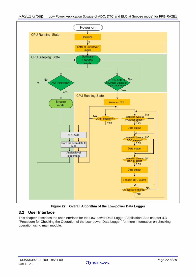
3. Low-power Data Logger Application This chapter describes the detailed design of the low-power data logger application using the module features described in the previous chapter.
3.1 Functional Specification This application project is implemented based on the following specifications. Figure 22 also shows the overall algorithm for the low-power data logger.
3.1.1 Data Acquisition Function • Analog signals of two sensors (Illuminance sensor Seeed Grove-Luminance Sensor, Temperature sensor
Seeed Grove-Temperature Sensor) connected to external pins are acquired by A/D converters. • Analog signal input values are between the low-potential reference voltage (VREFL and VSS) and the
high-potential reference voltage (VREFH and VCC) set between 0 V and 3.3 V respectively. • Acquisition of data from each sensor is performed every 30 minutes regardless of the low power mode
status (using Snooze request event or AGT1 underflow interrupt) • The size of the measurement data buffer is 96 samples (48 hours of sampling every 30 minutes). 3.1.2 Data Level Judgement Function • After acquiring the data, the analog signal pin AN001 judges the level by DOC. • When AN001 is equal to or greater than the threshold (30.00°C), the low power mode is canceled and
data is output. 3.1.3 Data Output Function • Perform data output every 24 hours triggered by RTC alarm interrupt, external IRQ interrupt, and DOC
interrupt. • UART communication format is 115,200 bps baud rate, 8-bit data length, no parity, 1 stop bit.
RA2E1 Group Low Power Application (Usage of ADC, DTC and ELC at Snooze mode) for FPB-RA2E1
R30AN0392EJ0100 Rev.1.00 Page 22 of 39 Oct.12.21
Figure 22. Overall Algorithm of the Low-power Data Logger
3.2 User Interface This chapter describes the user interface for the Low-power Data Logger Application. See chapter 4.3 "Procedure for Checking the Operation of the Low-power Data Logger” for more information on checking operation using main module.

RA2E1 Group Low Power Application (Usage of ADC, DTC and ELC at Snooze mode) for FPB-RA2E1
R30AN0392EJ0100 Rev.1.00 Page 23 of 39 Oct.12.21
Figure 23 shows the system overview of this application project.
Figure 23. System Overview
3.2.1 Connect the Sensor Figure 24 shows the connection diagram with the sensor. In this application project, attach Seeed's Grove Base Shield V2.0 for Arduino to Arduino compatible connector of the FPB-RA2E1 kit. Attach the sensor module to the A0 and A1 connectors of this Base Shield with Grove cable. This connects the analog signal pins (AN000 and AN001) of the RA2E1 MCU with the analog output pins of the two sensors.
• Light Sensor Module: Seeed Grove – Luminance Sensor • Equipped with illuminance sensor APDS-9002, Operating voltage: 2.4~5 V, Measurement range:
0~1000 Lux • Temperature Sensor Module: Seeed Grove – Temperature Sensor • Equipped with NTC thermistor NCP18WF104F03RC, Operating voltage: 3.3~5 V, Operating temperature
range: -40 °C ~125 °C
Figure 24. Sensor Connection
Seeed Grove
- Temperature Sensor V1.2
Seeed Grove
- Luminance Sensor
Seeed Grove Base Shield
V2.0 for Arduino
FPB-RA2E1 kit
USB – TTL connector
PC
Seeed Grove
- Temperature Sensor
Seeed Grove
- Luminance Sensor
Seeed Grove Base Shield
V2.0 for Arduino
FPB-RA2E1 kit
A0
A1

RA2E1 Group Low Power Application (Usage of ADC, DTC and ELC at Snooze mode) for FPB-RA2E1
R30AN0392EJ0100 Rev.1.00 Page 24 of 39 Oct.12.21
3.2.2 Connect the USB-TTL Connector Table 4 and Figure 25 show the connection pins to the USB-TTL connector. Connect Arduino compatible connector of FPB-RA2E1 kit using jumper wires.
Table 4. Pins to be Connected to the USB-TTL Connector (FPB-RA2E1 kit)
RA2E1 Pin FPB-RA2E1 Pin Typical Uses P101/TxD0 J1-4 Serial communication (transmission).
Connect to the RXD pin of the USB-TTL connector. VSS GND Ground.
Connect to the GND pin of the USB-TTL connector.
Figure 25. Connecting to the External Equipment
3.2.3 Data Communication Specifications This application project performs data communication according to the following procedure and format.
3.2.3.1 Communication Data Format • Transmission Format
Following is the packet format/protocol of data transmitted by the FPB-RA2E1. Packet format:
Description Code Length Function (a) Start code '^' 1 byte Start of the packet (b) Attribute code ASCII Code 1 byte Represent a data output occurrence event
'1': RTC alarm event '2': External IRQ event '3': DOC interrupt event
(c) Delimiter code ‘,’ 1 byte Code delimiting code (d) Data length code
ASCII Code 4 bytes Indicates the length of the data section.
(e) Data ASCII Code Number of bytes specified in (d)
See the following Data Format
(f) End code '$' 1 byte End of the packet (g) Linefeed code ‘\n’ 1 byte Linefeed
(a) Start code
(b) Attribute code
(c) Delimiter code
(d) Data length code
(c) Delimiter code
(e) Data
(f) End code
(g) Linefeed code
Serial Communications TX

RA2E1 Group Low Power Application (Usage of ADC, DTC and ELC at Snooze mode) for FPB-RA2E1
R30AN0392EJ0100 Rev.1.00 Page 25 of 39 Oct.12.21
(e) Data format
The format of the data part varies depending on the attribute code as shown below.
• Attribute code 1/2 (output data by RTC alarm and external IRQ interrupt) Format of data part:
Time data ‘,’ Number of data
',' First data
',' Second data
',' ・・・ ',' Last data
Light Data
'/' Temperature Data
• Attribute code 3 (output data by DOC interrupt) Format of data part:
Time data ',' Light data
'/' Temperature data
The data comprising the format of attribute codes 1 to 3 is generated as follows.
• The data count consists of 0 to 9 ASCII codes. The length is 2 bytes. Example: When the system transmits 10 data, it sets 0x31, 0x30.
• The time/light/temperature data consists of 0 to 9 ASCII codes. Example: When the system transmits a time value “1234”, it sets 0x31, 0x32, 0x33, 0x34.
• The time data is composed of 10-digit decimal number representing elapsed time. • The light and temperature data are composed of 4-digit decimal number representing ADC read value.
When the system transmits data “2000”, it sets 0x32, 0x30, 0x30, 0x30. • The delimiter between the code is ',', the delimiter between the time and light data is '/'. 3.2.4 Input/Output Pins for Debugging Table 5 and Figure 26 show the I/O pins for debugging this application project. The debug pins can be observed and toggled as shown below to cancel the low power modes and check the status of the modes.
Table 5. Debugging I/O Pins (FPB-RA2E1 kit)
RA2E1 Pin FPB-RA2E1 Pins or Connecting Components
Typical Uses
P109/CLKOUT J5-2 Clock output P914 LED2 Turn on in Normal mode P205/IRQ1 User switch S1 Manual cancellation of low power mode

RA2E1 Group Low Power Application (Usage of ADC, DTC and ELC at Snooze mode) for FPB-RA2E1
R30AN0392EJ0100 Rev.1.00 Page 26 of 39 Oct.12.21
Figure 26. Debugging I/O Pins (FPB-RA2E1 kit)
3.3 Clock Input The clock from the external oscillator must be input in order for the RTC or AGT to perform an accurate time count. FPB-RA2E1 kit implements a 32.768 KHz clock crystal, but by default, it is not connected to RA2E1 MCU by solder jumpers (E19 and E20). Therefore, the project attached with this application note selects an internal clock (LOCO) as the count source for AGT0 and RTC.
When accurate time counting is required, connect the external oscillator using solder bridges.
Also, the following settings should be changed:
• Change the sub-clock populating setting to “Populated” in the BSP tab in the FSP configurator. • Change the count source for AGT0 to “SUBCLOCK” in the Stacks tab in the FSP configurator. • Change the count source for RTC to the sub-clock in rtc_initialize() in app_common.c. Figure 27 and Figure 28 show the positions of the solder jumpers for external oscillator connections.
Figure 27. Solder Jumper for External Oscillator Connection
Manual cancellation of low power mode
Turn on in Normal mode
CLKOUT pin
E20
E19

RA2E1 Group Low Power Application (Usage of ADC, DTC and ELC at Snooze mode) for FPB-RA2E1
R30AN0392EJ0100 Rev.1.00 Page 27 of 39 Oct.12.21
Figure 28. Solder Jumper for External Oscillator Connection (circuit diagram)
3.4 Debugging This application project implements pin input/output function for checking the low power mode status, fast cycle debug function, and disable sensor dependent process function.
3.4.1 Canceling the Low Power Mode by Pressing Down the User Switch The user switch S1 of FPB-RA2E1 can be pressed to generate IRQ1 interrupt and cancel the low power mode. By setting a breakpoint after canceling, the program being executed is stopped, and each register and data can be checked.
3.4.2 Checking the Low Power Mode Status The low power mode status can be checked by observing LED2 and CLKOUT pin.
When LED2 is turned on, the mode is Normal. In Software Standby mode, HOCO, MOCO, and MOSC clocks are stopped. Therefore, when these clocks are set as the clock output source, CLKOUT pin retains either High or Low state. When toggling out, the mode is changed to Normal mode or the low power mode other than the Software Standby mode. When the debugger is connected, the clock does not stop even if Software Standby mode is entered. Disconnecting the debugger is required to check the mode status. In addition, the port P109 (CLKOUT pin) of the FPB-RA2E1 kit is connected to the onboard E2 emulator by default. If this pin is used for clock output, it should disconnect solder jumpers (E25 and E29) as needed.
Figure 31 shows the position of the solder jumper for connecting the P109 (CLKOUT pin) to the onboard E2 emulator.
Table 3.3 lists the pin output states in each low power mode, and Figure 29 and Figure 30 show examples of pin outputs in each low power mode.
Table 6. Pin Output States in each Low Power Mode
Low Power Modes P109/CLKOUT P504/LED2 Normal mode Toggle High Software Standby mode High or Low Low Snooze mode Toggle Low
Figure 29. Example of Pin Output in Snooze Mode
SW Standby Low Power Modes Snooze Software Standby

RA2E1 Group Low Power Application (Usage of ADC, DTC and ELC at Snooze mode) for FPB-RA2E1
R30AN0392EJ0100 Rev.1.00 Page 28 of 39 Oct.12.21
Figure 30. Example of Pin Output in Normal Mode
a
Figure 31. Solder Jumper for Connecting P109 to Onboard E2 Emulator (1) Fast Cycle Debug This sample project implements a function to speed up the execution cycle of data acquisition and data processing in order to check the operation in a short time. To enable this feature, define DEBUG_FAST_CYCLE macro in the app_common.h. When this DEBUG_FAST_CYCLE macro is defined, the following process is enabled, and the data acquisition period is set every 30 seconds and the data processing period is set every 30 minutes.
• Resetting the AGT0 timer count (AGT) • Changing the Added Value of the RTC Alarm Setting
SW Standby Low Power Modes Normal

RA2E1 Group Low Power Application (Usage of ADC, DTC and ELC at Snooze mode) for FPB-RA2E1
R30AN0392EJ0100 Rev.1.00 Page 29 of 39 Oct.12.21
3.5 Flowchart Figure 32 shows the overall flow of the application project.
Figure 32. Overall Flow

RA2E1 Group Low Power Application (Usage of ADC, DTC and ELC at Snooze mode) for FPB-RA2E1
R30AN0392EJ0100 Rev.1.00 Page 30 of 39 Oct.12.21
Figure 33 shows the module initialization processing flow.
Figure 33. Module Initialization Processing

RA2E1 Group Low Power Application (Usage of ADC, DTC and ELC at Snooze mode) for FPB-RA2E1
R30AN0392EJ0100 Rev.1.00 Page 31 of 39 Oct.12.21
Figure 34 shows the main loop processing flow.
Figure 34. Main Loop Processing

RA2E1 Group Low Power Application (Usage of ADC, DTC and ELC at Snooze mode) for FPB-RA2E1
R30AN0392EJ0100 Rev.1.00 Page 32 of 39 Oct.12.21
Figure 35 shows the flow of RTC alarm interrupt processing.
Figure 35. RTC Alarm Interrupt Processing Figure 36 shows the flowchart for IRQ interrupt processing.
Figure 36. IRQ Interrupt Processing Figure 37 shows the flowchart for DOC interrupt processing.
Figure 37. DOC Interrupt Processing Figure 38 shows the SCI interrupt processing flow.
Figure 38. SCI Interrupt Processing

RA2E1 Group Low Power Application (Usage of ADC, DTC and ELC at Snooze mode) for FPB-RA2E1
R30AN0392EJ0100 Rev.1.00 Page 33 of 39 Oct.12.21
Figure 39
Figure 39. Figure 3.18 shows the flow of data processing.

RA2E1 Group Low Power Application (Usage of ADC, DTC and ELC at Snooze mode) for FPB-RA2E1
R30AN0392EJ0100 Rev.1.00 Page 34 of 39 Oct.12.21
Figure 39. Data Processing
4. Evaluating Applications 4.1 Import and Building a Project To build an application project with e2studio IDE, proceed as follows:
1. Launch e2studio IDE. 2. Select any workspace in Workspace launcher. 3. Close Welcome window. 4. Select File > Import. 5. Select Existing Projects into Workspace from the Import dialog box. 6. Select archive file. 7. Select the project you want to import and click Finish. 8. Open configuration.xml and click Generate Project Content in the Configurator window 9. Select Project > Build Project. 4.2 Download and Debug a Project To download and debug an application project using e2studio and onboard E2 emulator, proceed as follows:
1. Connect the connector CN6 of FPB-RA2E1 and PC using USB cable. 2. Change setting of the header CN1 on the FPB-RA2E1 to a debugger enabling setting (connect pin 1 and
2). 3. Open Debug Configuration window. 4. Change settings as follows and as shown in Figure 40.
Debug hardware: E2 Lite (ARM) Power Target From The Emulator: No
5. Clicking Debug

RA2E1 Group Low Power Application (Usage of ADC, DTC and ELC at Snooze mode) for FPB-RA2E1
R30AN0392EJ0100 Rev.1.00 Page 35 of 39 Oct.12.21
Figure 40. Debug Configuration
4.3 Procedure for Checking the Operation of the Low-power Data Logger To check the operation of the low-power data logger, proceed as follows:
1. Connect the FPB-RA2E1 and PC using USB - TTL connector and jumper wires. Refer to Table 3.1 for detailed connections.
2. Launch a terminal software on PC and change the settings as follows: • Transfer speed: 115,200 bps • Data length: 8 bits • Parity: None • Stop-bit length: 1 bit 3. Referring to Chapter 4.5, change setting of the header CN1 on the FPB-RA2E1 to a free-run operation
setting. 4. Power on the kit. 5. Confirm the operation. This application project performs data output every 24 hours (every 24 minutes in fast cycle debug is enabled) (See Figure 41). In addition, data output is executed when the values of the light sensor and temperature sensor exceed the threshold value (See Figure 42). The outputted data can be viewed on terminal software on PC. Furthermore, by pressing the user switch S1 of the FPB-RA2E1 kit, the progress of accumulated measurement data can be output at any time (See Figure 43).

RA2E1 Group Low Power Application (Usage of ADC, DTC and ELC at Snooze mode) for FPB-RA2E1
R30AN0392EJ0100 Rev.1.00 Page 36 of 39 Oct.12.21
Note: A fast cycle debug is enabled
Figure 41. Example of Data Output Triggered by 24 Hours Pass
Note: A fast cycle debug is enabled
Figure 42. Example of Data Output Triggered by Analog Level Judgment Result
Note: A fast cycle debug is enabled
Figure 43. Example of Data Output Triggered by Pressing the User Switch
4.4 Evaluating the Current Consumption FPB-RA2E1 implements a resistor (R3) and test points (TP1 and TP2) for measuring the current of the MCU power of 3.3 V. When measuring the current amount of the MCU, remove resistor R3 and connect the measuring equipment to the test points.
See Figure 44 and Figure 45 for the location of TP1 and TP2.
Figure 44. MCU Current Measuring Points (Circuit Diagram)

RA2E1 Group Low Power Application (Usage of ADC, DTC and ELC at Snooze mode) for FPB-RA2E1
R30AN0392EJ0100 Rev.1.00 Page 37 of 39 Oct.12.21
Figure 45. MCU Current Measuring Points
4.5 Notes on Free-run Operation with the FPB-RA2E1 Kit If the FPB-RA2E1 runs Free-Run, connect pin 2 and 3 of the header CN1. By connecting these pins, the onboard E2 emulator is in a forced reset state, and it can operate alone without control from IDE.
See Figure 46 for the location of CN1.
Figure 46. Header CN1 for Force Reset of Onboard E2 Emulater
5. References • Renesas FSP User's Manual renesas.github.io/fsp • Renesas RA MCU datasheet Select the relevant MCUs from the www.renesas.com/ra • Example Projects github.com/renesas/ra-fsp-examples • Application Note: Getting Started with Low Power Applications for RA2L1/RA2E1 Group(R11AN0480)
Test points
Resistor R3
Header CN1

RA2E1 Group Low Power Application (Usage of ADC, DTC and ELC at Snooze mode) for FPB-RA2E1
R30AN0392EJ0100 Rev.1.00 Page 38 of 39 Oct.12.21
Website and Support Visit the following vanity URLs to learn about key elements of the RA family, download components and related documentation, and get support.
RA Product Information www.renesas.com/ra RA Product Support Forum www.renesas.com/ra/forum RA Flexible Software Package www.renesas.com/FSP Renesas Support www.renesas.com/support

RA2E1 Group Low Power Application (Usage of ADC, DTC and ELC at Snooze mode) for FPB-RA2E1
R30AN0392EJ0100 Rev.1.00 Page 39 of 39 Oct.12.21
Revision History
Rev. Date Description Page Summary
1.00 Oct.12.21 - Initial version

General Precautions in the Handling of Microprocessing Unit and Microcontroller Unit Products The following usage notes are applicable to all Microprocessing unit and Microcontroller unit products from Renesas. For detailed usage notes on the products covered by this document, refer to the relevant sections of the document as well as any technical updates that have been issued for the products.
1. Precaution against Electrostatic Discharge (ESD)
A strong electrical field, when exposed to a CMOS device, can cause destruction of the gate oxide and ultimately degrade the device operation. Steps
must be taken to stop the generation of static electricity as much as possible, and quickly dissipate it when it occurs. Environmental control must be
adequate. When it is dry, a humidifier should be used. This is recommended to avoid using insulators that can easily build up static electricity.
Semiconductor devices must be stored and transported in an anti-static container, static shielding bag or conductive material. All test and
measurement tools including work benches and floors must be grounded. The operator must also be grounded using a wrist strap. Semiconductor
devices must not be touched with bare hands. Similar precautions must be taken for printed circuit boards with mounted semiconductor devices. 2. Processing at power-on
The state of the product is undefined at the time when power is supplied. The states of internal circuits in the LSI are indeterminate and the states of
register settings and pins are undefined at the time when power is supplied. In a finished product where the reset signal is applied to the external reset
pin, the states of pins are not guaranteed from the time when power is supplied until the reset process is completed. In a similar way, the states of pins
in a product that is reset by an on-chip power-on reset function are not guaranteed from the time when power is supplied until the power reaches the
level at which resetting is specified. 3. Input of signal during power-off state
Do not input signals or an I/O pull-up power supply while the device is powered off. The current injection that results from input of such a signal or I/O
pull-up power supply may cause malfunction and the abnormal current that passes in the device at this time may cause degradation of internal
elements. Follow the guideline for input signal during power-off state as described in your product documentation. 4. Handling of unused pins
Handle unused pins in accordance with the directions given under handling of unused pins in the manual. The input pins of CMOS products are
generally in the high-impedance state. In operation with an unused pin in the open-circuit state, extra electromagnetic noise is induced in the vicinity of
the LSI, an associated shoot-through current flows internally, and malfunctions occur due to the false recognition of the pin state as an input signal
become possible. 5. Clock signals
After applying a reset, only release the reset line after the operating clock signal becomes stable. When switching the clock signal during program
execution, wait until the target clock signal is stabilized. When the clock signal is generated with an external resonator or from an external oscillator
during a reset, ensure that the reset line is only released after full stabilization of the clock signal. Additionally, when switching to a clock signal
produced with an external resonator or by an external oscillator while program execution is in progress, wait until the target clock signal is stable. 6. Voltage application waveform at input pin
Waveform distortion due to input noise or a reflected wave may cause malfunction. If the input of the CMOS device stays in the area between VIL
(Max.) and VIH (Min.) due to noise, for example, the device may malfunction. Take care to prevent chattering noise from entering the device when the
input level is fixed, and also in the transition period when the input level passes through the area between VIL (Max.) and VIH (Min.). 7. Prohibition of access to reserved addresses
Access to reserved addresses is prohibited. The reserved addresses are provided for possible future expansion of functions. Do not access these
addresses as the correct operation of the LSI is not guaranteed. 8. Differences between products
Before changing from one product to another, for example to a product with a different part number, confirm that the change will not lead to problems.
The characteristics of a microprocessing unit or microcontroller unit products in the same group but having a different part number might differ in terms
of internal memory capacity, layout pattern, and other factors, which can affect the ranges of electrical characteristics, such as characteristic values,
operating margins, immunity to noise, and amount of radiated noise. When changing to a product with a different part number, implement a system-
evaluation test for the given product.

© 2021 Renesas Electronics Corporation. All rights reserved.
Notice 1. Descriptions of circuits, software and other related information in this document are provided only to illustrate the operation of semiconductor products
and application examples. You are fully responsible for the incorporation or any other use of the circuits, software, and information in the design of your product or system. Renesas Electronics disclaims any and all liability for any losses and damages incurred by you or third parties arising from the use of these circuits, software, or information.
2. Renesas Electronics hereby expressly disclaims any warranties against and liability for infringement or any other claims involving patents, copyrights, or other intellectual property rights of third parties, by or arising from the use of Renesas Electronics products or technical information described in this document, including but not limited to, the product data, drawings, charts, programs, algorithms, and application examples.
3. No license, express, implied or otherwise, is granted hereby under any patents, copyrights or other intellectual property rights of Renesas Electronics or others.
4. You shall be responsible for determining what licenses are required from any third parties, and obtaining such licenses for the lawful import, export, manufacture, sales, utilization, distribution or other disposal of any products incorporating Renesas Electronics products, if required.
5. You shall not alter, modify, copy, or reverse engineer any Renesas Electronics product, whether in whole or in part. Renesas Electronics disclaims any and all liability for any losses or damages incurred by you or third parties arising from such alteration, modification, copying or reverse engineering.
6. Renesas Electronics products are classified according to the following two quality grades: “Standard” and “High Quality”. The intended applications for each Renesas Electronics product depends on the product’s quality grade, as indicated below. "Standard": Computers; office equipment; communications equipment; test and measurement equipment; audio and visual equipment; home
electronic appliances; machine tools; personal electronic equipment; industrial robots; etc. "High Quality": Transportation equipment (automobiles, trains, ships, etc.); traffic control (traffic lights); large-scale communication equipment; key
financial terminal systems; safety control equipment; etc. Unless expressly designated as a high reliability product or a product for harsh environments in a Renesas Electronics data sheet or other Renesas Electronics document, Renesas Electronics products are not intended or authorized for use in products or systems that may pose a direct threat to human life or bodily injury (artificial life support devices or systems; surgical implantations; etc.), or may cause serious property damage (space system; undersea repeaters; nuclear power control systems; aircraft control systems; key plant systems; military equipment; etc.). Renesas Electronics disclaims any and all liability for any damages or losses incurred by you or any third parties arising from the use of any Renesas Electronics product that is inconsistent with any Renesas Electronics data sheet, user’s manual or other Renesas Electronics document.
7. No semiconductor product is absolutely secure. Notwithstanding any security measures or features that may be implemented in Renesas Electronics hardware or software products, Renesas Electronics shall have absolutely no liability arising out of any vulnerability or security breach, including but not limited to any unauthorized access to or use of a Renesas Electronics product or a system that uses a Renesas Electronics product. RENESAS ELECTRONICS DOES NOT WARRANT OR GUARANTEE THAT RENESAS ELECTRONICS PRODUCTS, OR ANY SYSTEMS CREATED USING RENESAS ELECTRONICS PRODUCTS WILL BE INVULNERABLE OR FREE FROM CORRUPTION, ATTACK, VIRUSES, INTERFERENCE, HACKING, DATA LOSS OR THEFT, OR OTHER SECURITY INTRUSION (“Vulnerability Issues”). RENESAS ELECTRONICS DISCLAIMS ANY AND ALL RESPONSIBILITY OR LIABILITY ARISING FROM OR RELATED TO ANY VULNERABILITY ISSUES. FURTHERMORE, TO THE EXTENT PERMITTED BY APPLICABLE LAW, RENESAS ELECTRONICS DISCLAIMS ANY AND ALL WARRANTIES, EXPRESS OR IMPLIED, WITH RESPECT TO THIS DOCUMENT AND ANY RELATED OR ACCOMPANYING SOFTWARE OR HARDWARE, INCLUDING BUT NOT LIMITED TO THE IMPLIED WARRANTIES OF MERCHANTABILITY, OR FITNESS FOR A PARTICULAR PURPOSE.
8. When using Renesas Electronics products, refer to the latest product information (data sheets, user’s manuals, application notes, “General Notes for Handling and Using Semiconductor Devices” in the reliability handbook, etc.), and ensure that usage conditions are within the ranges specified by Renesas Electronics with respect to maximum ratings, operating power supply voltage range, heat dissipation characteristics, installation, etc. Renesas Electronics disclaims any and all liability for any malfunctions, failure or accident arising out of the use of Renesas Electronics products outside of such specified ranges.
9. Although Renesas Electronics endeavors to improve the quality and reliability of Renesas Electronics products, semiconductor products have specific characteristics, such as the occurrence of failure at a certain rate and malfunctions under certain use conditions. Unless designated as a high reliability product or a product for harsh environments in a Renesas Electronics data sheet or other Renesas Electronics document, Renesas Electronics products are not subject to radiation resistance design. You are responsible for implementing safety measures to guard against the possibility of bodily injury, injury or damage caused by fire, and/or danger to the public in the event of a failure or malfunction of Renesas Electronics products, such as safety design for hardware and software, including but not limited to redundancy, fire control and malfunction prevention, appropriate treatment for aging degradation or any other appropriate measures. Because the evaluation of microcomputer software alone is very difficult and impractical, you are responsible for evaluating the safety of the final products or systems manufactured by you.
10. Please contact a Renesas Electronics sales office for details as to environmental matters such as the environmental compatibility of each Renesas Electronics product. You are responsible for carefully and sufficiently investigating applicable laws and regulations that regulate the inclusion or use of controlled substances, including without limitation, the EU RoHS Directive, and using Renesas Electronics products in compliance with all these applicable laws and regulations. Renesas Electronics disclaims any and all liability for damages or losses occurring as a result of your noncompliance with applicable laws and regulations.
11. Renesas Electronics products and technologies shall not be used for or incorporated into any products or systems whose manufacture, use, or sale is prohibited under any applicable domestic or foreign laws or regulations. You shall comply with any applicable export control laws and regulations promulgated and administered by the governments of any countries asserting jurisdiction over the parties or transactions.
12. It is the responsibility of the buyer or distributor of Renesas Electronics products, or any other party who distributes, disposes of, or otherwise sells or transfers the product to a third party, to notify such third party in advance of the contents and conditions set forth in this document.
13. This document shall not be reprinted, reproduced or duplicated in any form, in whole or in part, without prior written consent of Renesas Electronics. 14. Please contact a Renesas Electronics sales office if you have any questions regarding the information contained in this document or Renesas
Electronics products.
(Note1) “Renesas Electronics” as used in this document means Renesas Electronics Corporation and also includes its directly or indirectly controlled subsidiaries.
(Note2) “Renesas Electronics product(s)” means any product developed or manufactured by or for Renesas Electronics. (Rev.5.0-1 October 2020)
Corporate Headquarters Contact information
TOYOSU FORESIA, 3-2-24 Toyosu, Koto-ku, Tokyo 135-0061, Japan www.renesas.com
For further information on a product, technology, the most up-to-date version of a document, or your nearest sales office, please visit: www.renesas.com/contact/.
Trademarks Renesas and the Renesas logo are trademarks of Renesas Electronics Corporation. All trademarks and registered trademarks are the property of their respective owners.
Related Documents