Carlos E. Saavedra Associate Professor Dept. of Electrical & Comp. Engineering Queen’s University, Kingston, Ontario CANADA IEEE International Microwave Symposium Montréal, Canada 18 June 2012 Low-Noise Downconverters through Mixer-LNA Integration

Welcome message from author
This document is posted to help you gain knowledge. Please leave a comment to let me know what you think about it! Share it to your friends and learn new things together.
Transcript

Carlos E. Saavedra
Associate ProfessorDept. of Electrical & Comp. Engineering
Queen’s University, Kingston, Ontario CANADA
IEEE International Microwave SymposiumMontréal, Canada
18 June 2012
Low-Noise Downconverters through Mixer-LNA Integration

IMS Workshop WMK – 18 June 2012
Outline•Motivation
• Theory
Ø understanding noise in double-balanced (Gilbert-cell) CMOS active mixers.
• Design studies:
Ø broadband low-noise mixer.
Ø low-noise self-oscillating mixer using a balanced VCO load.
2

IMS Workshop WMK – 18 June 2012 17
Design study # 1:
A broadband noise-cancelling mixer

IMS Workshop WMK – 18 June 2012 18
• For the RF stage, select an LNA topology
• Two basic LNA families in wide use today are:– noise-cancelling LNA’s [7]
– LNA’s with inductive degeneration
• Several noise optimization techniques exist if an LNA withinductive degeneration is chosen: – simultaneous noise and input matching technique [9]
– power constrained noise optimization [10]
– power constrained simultaneous noise and input matching [11]
Design study # 1
IMS Workshop WMK – 18 June 2012 19
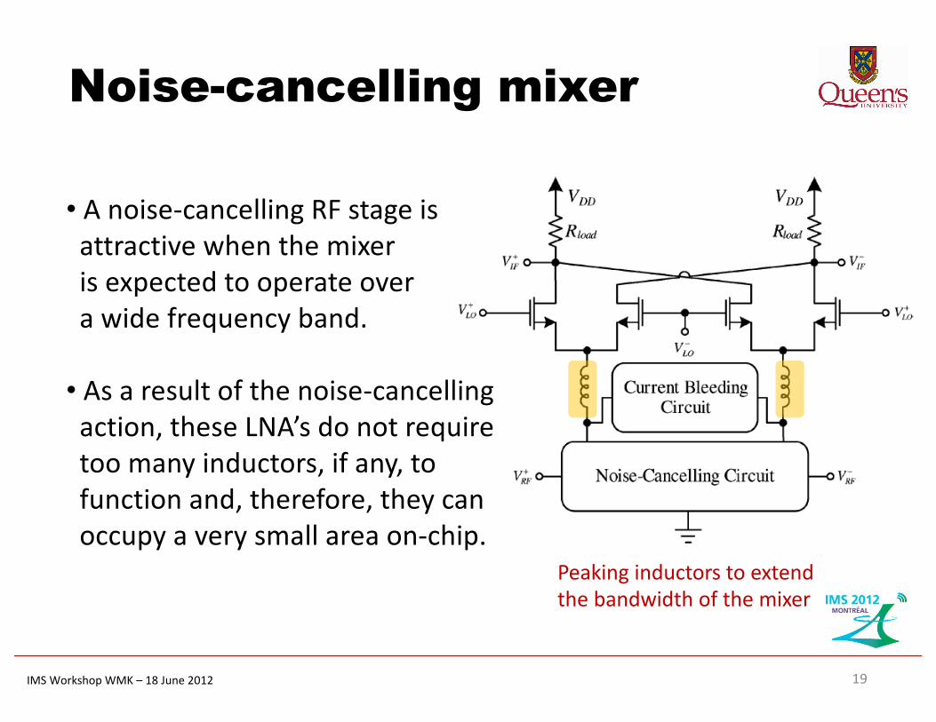
Noise-cancelling mixer
• A noise-cancelling RF stage isattractive when the mixeris expected to operate overa wide frequency band.
• As a result of the noise-cancelling action, these LNA’s do not requiretoo many inductors, if any, to function and, therefore, they canoccupy a very small area on-chip.
Peaking inductors to extendthe bandwidth of the mixer

IMS Workshop WMK – 18 June 2012 20
Noise-cancelling mixer
Full mixer schematic

IMS Workshop WMK – 18 June 2012 21
Half-circuit
• The signal voltages at nodes xand y are in-phase, but…
• The noise voltages at x and y are out-of-phase
• Thus, the noise currents from M1 subtract at node z:
• The key design equation is:
Low-noise RF stage
Noise-cancelling mixer

IMS Workshop WMK – 18 June 2012
The transconductor’s input impedance and gmeff are,
The noise currents associated with the transconductor are,
22
Noise-cancelling mixer
and its NF is,

IMS Workshop WMK – 18 June 2012
Noise-cancelling mixer
23
• Current bleeding circuit has
multiple benefits:
– allows for different bias currents
in the LO and the RF stage.
– LO switches can be biased with a
low overdrive voltage and they
can turn ON & OFF more quickly
– helps with 1/f noise
• Peaking inductor helps extend the
frequency response of the mixer.

IMS Workshop WMK – 18 June 2012
Noise-cancelling mixer
24
Measurements
Noise figure Conversion gain

IMS Workshop WMK – 18 June 2012
Noise-cancelling mixer
25
Measurements
IP1dB = -10.5 dBmIIP3 = +0.84 dBm
LO-RF isolation > 55 dBS11 (RF port) < - 8.8 dB

IMS Workshop WMK – 18 June 2012
Noise-cancelling mixer
26
S. S. K. Ho and C. E. Saavedra, “A CMOS Broadband Low-Noise Mixer with Noise Cancellation”, IEEE Transactions on Microwave Theory and Techniques, vol. 58, no. 5, pp. 1126-1132, May 2010.

IMS Workshop WMK – 18 June 2012 27
Design study # 2:
Low-noise self-oscillating mixer (SOM) using a balanced VCO load

IMS Workshop WMK – 18 June 2012
Design study # 2
28
Monolithic integration gives RFIC designers the ability to
merge different transceiver components to create a more
compact solution that saves dc power and chip area.
Enter….
self-oscillating mixers
SOM’s can be implemented using different configurations that
can result in interesting design possibilities.

IMS Workshop WMK – 18 June 2012 29
Design study # 2
Basic configuration RF/LO-swap [12]
Combined LO/IF Network

IMS Workshop WMK – 18 June 2012
Low-noise SOM
30
The RF transconductor
• An LNA-type structure usingthe simultaneous noise and input match technique ischosen for this design.
• Devices M7 and M8 arefor current bleeding, whosebenefits were discussed in Design Study #1.
• Lshunt resonates with the tail capacitance of the switchingcore and therefore helps to alleviate 1/f noise.

IMS Workshop WMK – 18 June 2012 31
Low-noise SOMOscillator subcircuit – design choices
• Where to connect the oscillator to themixer? (already discussed on p. 30)
• Which type of oscillator topologyto use?
• Within the LC-tank oscillator family,topologies abound. Yet, if oscillator tunability is desired, the general circuit to the right is a good candidate.

IMS Workshop WMK – 18 June 2012
Low-noise SOM
32
• The oscillator on the previous slide has a single tail current, yet the mixer in question needs to see a balanced load.
• This can be fixed by realizing that the cross coupled transistors can be split as shown in the figure below:

IMS Workshop WMK – 18 June 2012
Low-noise SOM
33
Full SOM schematic

IMS Workshop WMK – 18 June 2012
Low-noise SOM
34
• Current flows in the SOM circuit when VLO+ is high.
• Nodes “plus” and “minus” actas a differential terminal for theIF currents.
• The situation is reversed whenthe LO waveform has the oppositephase.
IMS Workshop WMK – 18 June 2012
Low-noise SOM
35
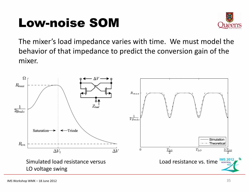
The mixer’s load impedance varies with time. We must model thebehavior of that impedance to predict the conversion gain of themixer.
Simulated load resistance versus LO voltage swing
Load resistance vs. time

IMS Workshop WMK – 18 June 2012
Low-noise SOM
36
• Using Fourier analysis, Rload can be written as:
where and
• The effective gm of the RF stage is:
• The conversion gain of the SOM is:
• Keeping only the first terms of Rload leads to:
IMS Workshop WMK – 18 June 2012
Low-noise SOM
37
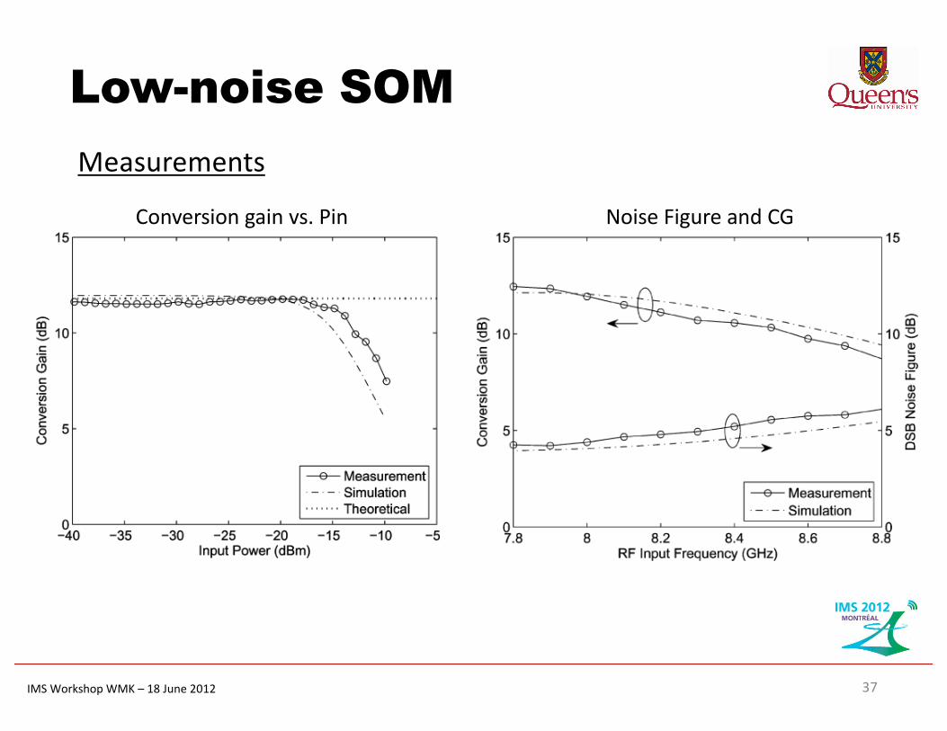
Measurements
Conversion gain vs. Pin Noise Figure and CG

IMS Workshop WMK – 18 June 2012
Low-noise SOM
38
Measurements
Power performance Two-tone test

IMS Workshop WMK – 18 June 2012
Low-noise SOM
39
Measurements
Oscillator phase noise VCO tuning range

IMS Workshop WMK – 18 June 2012
Low-noise SOM
40
S. S. K. Ho and C. E. Saavedra, “A Low-Noise Self-Oscillating Mixer using a Balanced VCO Load”, IEEE Transactions on Circuits and Systems I: Regular Papers, vol. 58, no. 8, pp. 1705-1712, August 2011.
Measurements
RF return loss
IMS Workshop WMK – 18 June 2012
• To reduce the noise figure of a CMOS double-balanced mixer, the RFIC designer should focus on: – minimizing the noise contribution of the RF transconductance stage
– ensuring that the mixing core is driven by an LO signal with fast transitions
• Any one of a number of LNA topologies can be used for the RF stage of the mixer. A noise-cancelling configuration, for example, can produce very broadband operation.
• Incorporating current bleeding into the mixer can help reduce 1/f noise and it also gives the designer more freedom to chose the bias currents in the RF and LO stages.
• SOM’s, in which a mixer, an LNA and an oscillator are merged into one unit open innovative design opportunities.
Final remarks
41
IMS Workshop WMK – 18 June 2012
References1. M. T. Terrovitis and R. G. Meyer, “Noise in Current-Commutating Mixers”, IEEE Journal of Solid-State
Circuits, vol. 34, no. 6, pp. 772-782, June 1999.2. H. Darabi and A. A. Abidi, “Noise in RF-CMOS Mixers: A Simple Physical Model”, IEEE Journal of Solid-State
Circuits, vol. 35, no. 1, pp. 15-25, Jan. 2000.3. H. Sjoland, A. Karimi-Sanjaani and A. A. Abidi, “A Merged CMOS LNA and Mixer for a WCDMA Receiver”
IEEE Journal of Solid-State Circuits, vol. 38, no. 6, pp. 1045-1050, June 2003.4. A. Amer, E. Hegazi and H. Ragaie, “A 90-nm Wideband Merged CMOS LNA and Mixer Exploiting Noise
Cancellation,” IEEE Journal of Solid-State Circuits, vol. 42, no. 2, pp. 323-328, February 2007.5. S. S. K. Ho and C. E. Saavedra, “A CMOS Broadband Low-Noise Mixer with Noise Cancellation”, IEEE
Transactions on Microwave Theory and Techniques, vol. 58, no. 5, pp. 1126-1132, May 2010.6. S.-G. Lee and J.-K. Choi, “Current-reuse bleeding mixer," Electronics Letters, 36(8), pp. 696-697, Apr 2000.7. W.-H. Chen, G. Liu, B. Zdravko and A. Niknejad, “A highly linear broadband CMOS LNA employing noise
cancellation”, IEEE J. Solid-State Circuits, vol. 43, no. 5, pp. 1164-1176, May 2008.8. S. S. K. Ho and C. E. Saavedra, “A Low-Noise Self-Oscillating Mixer using a Balanced VCO Load”, IEEE
Transactions on Circuits and Systems I: Regular Papers, vol. 58, no. 8, pp. 1705-1712, August 2011.9. S. P. Voinigescu et al., “A scalable high-frequency noise model for bipolar transistors with application
optimal transistor sizing for low-noise amplifier design,” IEEE Journal of Solid-State Circuits , vol. 32, pp. 1430–1439, Sept. 1997.
10. D. Shaeffer and T. Lee, "A 1.5-v, 1.5-ghz cmos low noise amplifer," IEEE Journal of Solid-State Circuits, vol. 32, no. 5, pp. 745-759, May 1997.
11. P. Andreani et al., “Noise optimization of an inductively degenerated CMOS low noise amplifier,” IEEE Transactions on Circuits and Systems II, vol. 48, pp. 835–841, Sept. 2001.
12. B. R. Jackson and C. E. Saavedra, "A Dual-Band Self-Oscillating Mixer for C-Band and X-Band Appli-cations," IEEE Transactions on Microwave Theory and Techniques, Vol. 58, No. 2, pp. 318-323, 2010.
42

IMS Workshop WMK – 18 June 2012 43
This workshop was sponsored by the
IEEE MTT-S Technical Coordinating Committee 22:
Signal Generation and Frequency Conversion
http://www.mtt-archives.org/~mtt22/
Related Documents