R1 294 kW V 15 V/50 mA O TPS61093 CP1 CP2 SW FB EN OUT VO VIN GND SS C1 4.7 F m R2 10.2 kW L1 10 H m V 1.6 V to 6 V I R3 200 kW C5 1 F m C3 100 nF C2 0.1 F m C4 1 F m Product Folder Sample & Buy Technical Documents Tools & Software Support & Community TPS61093-Q1 SLVSCO6 – JANUARY 2015 TPS61093-Q1 Low Input Boost Converter With Integrated Power Diode and Input/Output Isolation 1 Features 3 Description The TPS61093-Q1 is a 1.2-MHz, fixed-frequency 1• AEC-Q100 Qualified with the Following Results: boost converter designed for high integration and – Device Temperature Grade 1: -40°C to 125°C high reliability. The IC integrates a 20-V power Junction Operating Temperature Range switch, input/output isolation switch, and power diode. • Input Range: 1.6-V to 6-V When the output current exceeds the overload limit, the isolation switch of the IC opens up to disconnect • Integrated Power Diode and Isolation FET the output from the input. This disconnection protects • 20-V Internal Switch FET With 1.1-A Current the IC and the input supply. The isolation switch also • Fixed 1.2-MHz Switching Frequency disconnects the output from the input during shut down to minimize leakage current. When the IC is • Efficiency at 15-V Output up to 88% shutdown, the output capacitor is discharged to a low • Overload and Overvoltage Protection voltage level by internal diodes. Other protection • Programmable Soft Start-up features include 1.1-A peak overcurrent protection • Load Discharge Path After IC Shutdown (OCP) at each cycle, output overvoltage protection (OVP), thermal shutdown, and undervoltage lockout • 2.5 × 2.5 × 0.8 mm SON Package (UVLO). 2 Applications With its 1.6-V minimum input voltage, the IC can be powered by two alkaline batteries, a single Li-ion • OLED Power Supply battery, or 3.3-V and 5-V regulated supply. The • 3.3-V to 12-V, 5-V to 12-V Boost Converter output can be boosted up to 17-V. The TPS61093-Q1 is available in 2.5 mm × 2.5 mm SON package with thermal pad. Device Information (1) PART NUMBER PACKAGE BODY SIZE (NOM) TPS61093-Q1 SON (10) 2.50 mm x 2.50 mm (1) For all available packages, see the orderable addendum at the end of the data sheet. 4 Simplified Schematic 1 An IMPORTANT NOTICE at the end of this data sheet addresses availability, warranty, changes, use in safety-critical applications, intellectual property matters and other important disclaimers. PRODUCTION DATA.

Welcome message from author
This document is posted to help you gain knowledge. Please leave a comment to let me know what you think about it! Share it to your friends and learn new things together.
Transcript

R1
294 kW
V 15 V/50 mAO
TPS61093
CP1
CP2
SW
FBEN
OUT
VO
VIN
GNDSS
C1
4.7 Fm
R2
10.2 kW
L1
10 Hm
V 1.6 V to 6 VI
R3200 kW
C5
1 Fm
C3 100 nFC2 0.1 Fm
C4
1 Fm
Product
Folder
Sample &Buy
Technical
Documents
Tools &
Software
Support &Community
TPS61093-Q1SLVSCO6 –JANUARY 2015
TPS61093-Q1 Low Input Boost ConverterWith Integrated Power Diode and Input/Output Isolation
1 Features 3 DescriptionThe TPS61093-Q1 is a 1.2-MHz, fixed-frequency
1• AEC-Q100 Qualified with the Following Results:boost converter designed for high integration and– Device Temperature Grade 1: -40°C to 125°C high reliability. The IC integrates a 20-V power
Junction Operating Temperature Range switch, input/output isolation switch, and power diode.• Input Range: 1.6-V to 6-V When the output current exceeds the overload limit,
the isolation switch of the IC opens up to disconnect• Integrated Power Diode and Isolation FETthe output from the input. This disconnection protects• 20-V Internal Switch FET With 1.1-A Current the IC and the input supply. The isolation switch also
• Fixed 1.2-MHz Switching Frequency disconnects the output from the input during shutdown to minimize leakage current. When the IC is• Efficiency at 15-V Output up to 88%shutdown, the output capacitor is discharged to a low• Overload and Overvoltage Protection voltage level by internal diodes. Other protection
• Programmable Soft Start-up features include 1.1-A peak overcurrent protection• Load Discharge Path After IC Shutdown (OCP) at each cycle, output overvoltage protection
(OVP), thermal shutdown, and undervoltage lockout• 2.5 × 2.5 × 0.8 mm SON Package(UVLO).
2 Applications With its 1.6-V minimum input voltage, the IC can bepowered by two alkaline batteries, a single Li-ion• OLED Power Supply battery, or 3.3-V and 5-V regulated supply. The
• 3.3-V to 12-V, 5-V to 12-V Boost Converter output can be boosted up to 17-V. The TPS61093-Q1is available in 2.5 mm × 2.5 mm SON package withthermal pad.
Device Information (1)
PART NUMBER PACKAGE BODY SIZE (NOM)TPS61093-Q1 SON (10) 2.50 mm x 2.50 mm
(1) For all available packages, see the orderable addendum atthe end of the data sheet.
4 Simplified Schematic
1
An IMPORTANT NOTICE at the end of this data sheet addresses availability, warranty, changes, use in safety-critical applications,intellectual property matters and other important disclaimers. PRODUCTION DATA.

TPS61093-Q1SLVSCO6 –JANUARY 2015 www.ti.com
Table of Contents8.2 Functional Block Diagram ......................................... 81 Features .................................................................. 18.3 Feature Description................................................... 92 Applications ........................................................... 18.4 Device Functional Modes.......................................... 93 Description ............................................................. 1
9 Application and Implementation ........................ 104 Simplified Schematic............................................. 19.1 Application Information............................................ 105 Revision History..................................................... 29.2 Typical Applications ................................................ 106 Pin Configuration and Functions ......................... 3
10 Power Supply Recommendations ..................... 177 Specifications......................................................... 411 Layout................................................................... 177.1 Absolute Maximum Ratings ...................................... 4
11.1 Layout Guidelines ................................................. 177.2 ESD Ratings.............................................................. 411.2 Layout Example .................................................... 177.3 Recommended Operating Conditions....................... 411.3 Thermal Considerations ........................................ 187.4 Thermal Information .................................................. 4
12 Device and Documentation Support ................. 197.5 Electrical Characteristics........................................... 512.1 Trademarks ........................................................... 197.6 Timing Requirements ................................................ 512.2 Electrostatic Discharge Caution............................ 197.7 Typical Characteristics .............................................. 612.3 Glossary ................................................................ 198 Detailed Description .............................................. 8
13 Mechanical, Packaging, and Orderable8.1 Overview ................................................................... 8Information ........................................................... 19
5 Revision History
DATE REVISION NOTESJanuary 2015 * Initial Release
2 Submit Documentation Feedback Copyright © 2015, Texas Instruments Incorporated
Product Folder Links: TPS61093-Q1
FB
VO
SW
OUT
SS
CP1
GND
VIN
EN
CP2
6
10
5
1
Thermal
Pad
TPS61093-Q1www.ti.com SLVSCO6 –JANUARY 2015
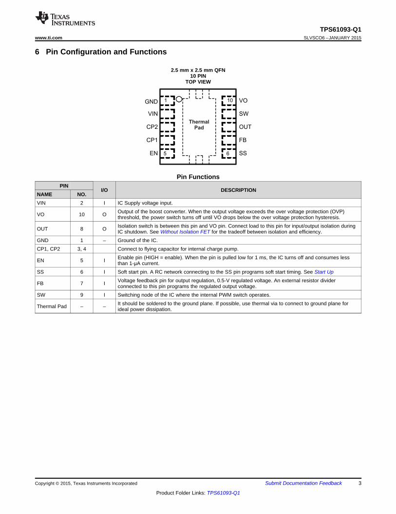
6 Pin Configuration and Functions
2.5 mm x 2.5 mm QFN10 PIN
TOP VIEW
Pin FunctionsPIN
I/O DESCRIPTIONNAME NO.VIN 2 I IC Supply voltage input.
Output of the boost converter. When the output voltage exceeds the over voltage protection (OVP)VO 10 O threshold, the power switch turns off until VO drops below the over voltage protection hysteresis.Isolation switch is between this pin and VO pin. Connect load to this pin for input/output isolation duringOUT 8 O IC shutdown. See Without Isolation FET for the tradeoff between isolation and efficiency.
GND 1 – Ground of the IC.CP1, CP2 3, 4 Connect to flying capacitor for internal charge pump.
Enable pin (HIGH = enable). When the pin is pulled low for 1 ms, the IC turns off and consumes lessEN 5 I than 1-μA current.SS 6 I Soft start pin. A RC network connecting to the SS pin programs soft start timing. See Start Up
Voltage feedback pin for output regulation, 0.5-V regulated voltage. An external resistor dividerFB 7 I connected to this pin programs the regulated output voltage.SW 9 I Switching node of the IC where the internal PWM switch operates.
It should be soldered to the ground plane. If possible, use thermal via to connect to ground plane forThermal Pad – – ideal power dissipation.
Copyright © 2015, Texas Instruments Incorporated Submit Documentation Feedback 3
Product Folder Links: TPS61093-Q1
TPS61093-Q1SLVSCO6 –JANUARY 2015 www.ti.com
7 Specifications
7.1 Absolute Maximum Ratingsover operating free-air temperature range (unless otherwise noted) (1)
MIN MAX UNITSupply voltage on pin VIN (2) –0.3 7 VVoltage on pins CP2, EN, and SS (2) –0.3 7 VVoltage on pin CP1 and FB (2) –0.3 3 VVoltage on pin SW, VO, and OUT (2) –0.3 20 VOperating Junction Temperature Range -40 150 °CTstg, Storage temperature range -55 150 °C
(1) Stresses beyond those listed under Absolute Maximum Ratings may cause permanent damage to the device. These are stress ratingsonly and functional operation of the device at these or any other conditions beyond those indicated under Recommended OperatingConditions is not implied. Exposure to absolute-maximum-rated conditions for extended periods may affect device reliability.
(2) All voltage values are with respect to network ground terminal.
7.2 ESD RatingsVALUE UNIT
Human body model (HBM), per AEC Q100-002 (1) ±2000V(ESD) Electrostatic discharge Corner pins (1, 5, 6, and 10) ±750 VCharged device model (CDM),
per AEC Q100-011 Other pins ±500
(1) AEC Q100-002 indicates HBM stressing is done in accordance with the ANSI/ESDA/JEDEC JS-001 specification.
7.3 Recommended Operating Conditionsover operating free-air temperature range (unless otherwise noted)
MIN NOM MAX UNITVi Input voltage range 1.6 6 VVo Output voltage range at VO pin 17 VL Inductor (1) 2.2 4.7 10 μHCin Input capacitor 4.7 μFCo Output capacitor at OUT pin (1) 1 10 μFCfly Flying capacitor at CP1 and CP2 pins 10 nFTJ Operating junction temperature –40 125 °CTA Operating ambient temperature –40 125 °C
(1) These values are recommended values that have been successfully tested in several applications. Other values may be acceptable inother applications but should be fully tested by the user.
7.4 Thermal InformationTPS60193-Q1
THERMAL METRIC (1) DSK UNIT10 PINS
RθJA Junction-to-ambient thermal resistance 49.2RθJC(top) Junction-to-case (top) thermal resistance 63.3RθJB Junction-to-board thermal resistance 23.4
°C/WψJT Junction-to-top characterization parameter 1.1ψJB Junction-to-board characterization parameter 23.0RθJC(bot) Junction-to-case (bottom) thermal resistance 5.7
(1) For more information about traditional and new thermal metrics, see the IC Package Thermal Metrics application report, SPRA953.
4 Submit Documentation Feedback Copyright © 2015, Texas Instruments Incorporated
Product Folder Links: TPS61093-Q1

TPS61093-Q1www.ti.com SLVSCO6 –JANUARY 2015
7.5 Electrical CharacteristicsVIN = 3.6 V, EN = VIN, TA = TJ = –40°C to 125°C, typical values are at TA = 25°C (unless otherwise noted)
PARAMETER TEST CONDITIONS MIN TYP MAX UNITSUPPLY CURRENTVIN Input voltage range, VIN 1.6 6 VIQ Operating quiescent current into VIN Device PWM switching no load 0.9 1.5 mAISD Shutdown current EN = GND, VIN = 6 V 5 μAUVLO Undervoltage lockout threshold VIN falling 1.5 1.55 VVhys Undervoltage lockout hysterisis 50 mVENABLE AND PWM CONTROLVENH EN logic high voltage VIN = 1.6 V to 6 V 1.2 VVENL EN logic low voltage VIN = 1.6 V to 6 V 0.3 VREN EN pull down resistor 400 800 1600 kΩVOLTAGE CONTROLVREF Voltage feedback regulation voltage 0.49 0.5 0.51 VIFB Voltage feedback input bias current 100 nAfS Oscillator frequency 1.0 1.2 1.4 MHzDmax Maximum duty cycle VFB = 0.1 V 90% 93%POWER SWITCH, ISOLATION FETRDS(ON)N N-channel MOSFET on-resistance VIN = 3 V 0.25 0.4 ΩRDS(ON)iso Isolation FET on-resistance VO = 5 V 2.5 4 Ω
VO = 3.5 V 4.5ILN_N N-channel leakage current VDS = 20 V 3 μAILN_iso Isolation FET leakage current VDS = 20 V 1 μAVF Power diode forward voltage Current = 500 mA 0.8 VOC, ILIM, OVP SC AND SSILIM N-Channel MOSFET current limit 0.9 1.1 1.6 AVovp Over voltage protection threshold Measured on the VO pin 18 19 VVovp_hys Over voltage protection hysteresis 0.6 VIOL Over load protection 200 300 mATHERMAL SHUTDOWNTshutdown Thermal shutdown threshold 150 °CThysteresis Thermal shutdown hysteresis 15 °C
7.6 Timing RequirementsVIN = 3.6 V, EN = VIN, TA = TJ = –40°C to 125°C, typical values are at TA = 25°C (unless otherwise noted)
PARAMETER TEST CONDITIONS MIN TYP MAX UNITToff EN pulse width to shutdown EN high to low 1 msTmin_on Minimum on pulse width 65 ns
Copyright © 2015, Texas Instruments Incorporated Submit Documentation Feedback 5
Product Folder Links: TPS61093-Q1

499
499.5
500
500.5
501
501.5
502
1.6 2 2.4 2.8 3.2 3.6 4 4.4 4.8 5.2 5.6 6
V - Input Voltage - VI
VF
B -
mV
0.498
0.499
0.5
0.501
0.502
-40 -20 0 20 40 60 80 100 120
T - Free-Air Temperature - ºCA
VF
B -
V
1 10 100 1000
Load - mA
40
45
55
60
65
70
75
80
85
90
100
Eff
icie
ncy -
%
50
95
V =1.8 VI
V = 2.5 VI
V = 3.3 VI
V = 4.2 VI
1 10 100 1000
Load - mA
40
45
55
60
65
70
75
80
85
90
100
Eff
icie
ncy -
%
50
95
V =1.8 VI
V = 2.5 VI
V = 3.3 VI
V = 4.2 VI
TPS61093-Q1SLVSCO6 –JANUARY 2015 www.ti.com
7.7 Typical CharacteristicsTable 1. Table Of Graphs
Figure 1, L = TOKO #A915_Y-100M, unless otherwise noted FIGUREη Efficiency vs Load current at OUT = 15 V Figure 1η Efficiency vs Load current at OUT = 10 V Figure 2
VFB FB voltage vs Free-air temperature Figure 3VFB FB voltage vs Input voltage Figure 4ILIM Switch current limit vs Free-air temperature Figure 5
Line transient response VIN = 3.3 V to 3.6 V; Load = 50 mA Figure 10Load transient response VIN = 2.5 V; Load = 10 mA to 50 mA; Cff = 100 pF Figure 11
PWM control in CCM VIN = 3.6 V; Load = 50 mA Figure 12PWM control in DCM VIN = 3.6 V; Load = 1 mA Figure 13
Pulse skip mode VIN = 4.5 V; OUT = 10 V; No load Figure 14Soft start-up VIN = 3.6 V; Load = 50 mA Figure 15
OUT = 15V OUT = 10V
Figure 1. Efficiency vs. Load Figure 2. Efficiency vs. Load
Figure 3. FB Voltage vs. Free-Air Temperature Figure 4. FB Voltage vs. Input Voltage
6 Submit Documentation Feedback Copyright © 2015, Texas Instruments Incorporated
Product Folder Links: TPS61093-Q1

0.8
0.9
1
1.1
1.2
1.3
-40 -20 0 20 40 60 80 100 120
T - Free-Air Temperature - ºCA
ILIM
-A
TPS61093-Q1www.ti.com SLVSCO6 –JANUARY 2015
Figure 5. Switch Current Limit vs. Free-Air Temperature
Copyright © 2015, Texas Instruments Incorporated Submit Documentation Feedback 7
Product Folder Links: TPS61093-Q1

OUTSW
Ramp
Generator
Oscillator
Current Sensor
FB
GND
+
EA
PWM Control
CP1CP2EN
Gate
Driver
Ref.
VO
VIN
Gate
Driver
Precharge
On/off control
EN
SS
SoftStartup
C/P
TPS61093-Q1SLVSCO6 –JANUARY 2015 www.ti.com
8 Detailed Description
8.1 OverviewThe TPS61093-Q1 is a highly integrated boost regulator for up to 17-V output. In addition to the on-chip 1-APWM switch and power diode, this IC also integrates an output-side isolation switch as shown in the functionalblock diagram. One common issue with conventional boost regulators is the conduction path from input to outputeven when the PWM switch is turned off. It creates three problems, which are inrush current during start-up,output leakage current during shutdown, and excessive over load current. In the TPS61093-Q1, the isolationswitch turns off under shutdown-mode and over load conditions, thereby opening the current path. However,shorting the VO and OUT pins bypasses the isolation switch and enhances efficiency. Because the isolationswitch is on the output side, the IC's VIN pin and power stage input power (up to 10 V) can be separated.
The TPS61093-Q1 adopts current-mode control with constant pulse-width-modulation (PWM) frequency. Theswitching frequency is fixed at 1.2-MHz typical. PWM operation turns on the PWM switch at the beginning ofeach switching cycle. The input voltage is applied across the inductor and the inductor current ramps up. In thismode, the output capacitor is discharged by the load current. When the inductor current hits the threshold set bythe error amplifier output, the PWM switch is turned off, and the power diode is forward-biased. The inductortransfers its stored energy to replenish the output capacitor. This operation repeats in the next switching cycle.The error amplifier compares the FB-pin voltage with an internal reference, and its output determines the dutycycle of the PWM switching. This closed-loop system requires frequency compensation for stable operation. Thedevice has a built-in compensation circuit that can accommodate a wide range of input and output voltages. Toavoid the sub-harmonic oscillation intrinsic to current-mode control, the IC also integrates slope compensation,which adds an artificial slope to the current ramp.
8.2 Functional Block Diagram
8 Submit Documentation Feedback Copyright © 2015, Texas Instruments Incorporated
Product Folder Links: TPS61093-Q1
TPS61093-Q1www.ti.com SLVSCO6 –JANUARY 2015
8.3 Feature Description
8.3.1 Shutdown And Load DischargeWhen the EN pin is pulled low for 1-ms, the IC stops the PWM switch and turns off the isolation switch, providingisolation between input and output. The internal current path consisting of the isolation switch’s body diode andseveral parasitic diodes quickly discharges the output voltage to less than 3.3-V. Afterwards, the voltage is slowlydischarged to zero by the leakage current. This protects the IC and the external components from high voltage inshutdown mode.
In shutdown mode, less than 5-μA of input current is consumed by the IC.
8.3.2 Over Load And Over Voltage ProtectionIf the over load current passing through the isolation switch is above the over load limit (IOL) for 3-μs (typ), theTPS61093-Q1 is switched off until the fault is cleared and the EN pin toggles. The function only is triggered 52-ms after the IC is enabled.
To prevent the PWM switch and the output capacitor from exceeding maximum voltage ratings, an over voltageprotection circuit turns off the boost switch as soon as the output voltage at the VO pin exceeds the OVPthreshold. Simultaneously, the IC opens the isolation switch. The regulator resumes PWM switching after the VOpin voltage falls 0.6-V below the threshold.
8.3.3 Under Voltage Lockout (UVLO)An under voltage lockout prevents improper operation of the device for input voltages below 1.55-V. When theinput voltage is below the under voltage threshold, the entire device, including the PWM and isolation switches,remains off.
8.3.4 Thermal ShutdownAn internal thermal shutdown turns off the isolation and PWM switches when the typical junction temperature of150°C is exceeded. The thermal shutdown has a hysteresis of 15°C, typical.
8.4 Device Functional ModesThe converter operates in continuous conduction mode (CCM) as soon as the input current increases above halfthe ripple current in the inductor, for lower load currents it switches into discontinuous conduction mode (DCM). Ifthe load is further reduced, the part starts to skip pulses to maintain the output voltage.
Copyright © 2015, Texas Instruments Incorporated Submit Documentation Feedback 9
Product Folder Links: TPS61093-Q1

R1
294kW
V 15V/50mAo
TPS61093
CP1
CP2
SW
FBEN
OUT
VO
VIN
GNDSS
C1
4.7 Fm
R2
10.2kW
L1
10 Hm
V 1.8V to 6Vin
R3
200kW
C5
1 Fm
C3 100nF C2 0.1 Fm
C4
100 Fm
C6
10nF
TPS61093-Q1SLVSCO6 –JANUARY 2015 www.ti.com
9 Application and Implementation
9.1 Application InformationThe following section provides a step-by-step design approach for configuring the TPS61093-Q1 as a voltageregulating boost converter, as shown in Figure 6.
9.2 Typical Applications
9.2.1 15V Output Boost Converter
Figure 6. 15V Boost Converter with 100µF Output Capacitor
9.2.1.1 Design Requirements
Table 2. Design ParametersPARAMETERS VALUES
Input voltage 4.2 VOutput voltage 15 V
Operating frequency 1.2 MHz
10 Submit Documentation Feedback Copyright © 2015, Texas Instruments Incorporated
Product Folder Links: TPS61093-Q1

0 50 100 150 200 250 300
Load - mA
40
45
50
60
70
85
90
100
Eff
icie
ncy -
%
95
80
75
65
55
Without isolation
With isolation
TPS61093
OUT
FB
R1
R2
CffOption C4
VO
C2
OUT
FB
R1
R2
CffOption
VO
C2
TPS61093
(a) With isolation FET (b) Without isolation FET
R1Vout = 0.5 V +1
R2
VoutR1 = R2 1
0.5 V
æ ö´ ç ÷
è ø
æ ö´ -ç ÷
è ø
TPS61093-Q1www.ti.com SLVSCO6 –JANUARY 2015
9.2.1.2 Detailed Design Procedure
9.2.1.2.1 Output Program
To program the output voltage, select the values of R1 and R2 (see Figure 7) according to Equation 1.
(1)
A recommended value for R2 is approximately 10-kΩ which sets the current in the resistor divider chain to0.5V/10kΩ = 50-μA. The output voltage tolerance depends on the VFB accuracy and the resistor divider.
Figure 7. Resistor Divider to Program Output Voltage
9.2.1.2.2 Without Isolation FET
The efficiency of the TPS61093-Q1 can be improved by connecting the load to the VO pin instead of the OUTpin. The power loss in the isolation FET is then negligible, as shown in Figure 8. The tradeoffs when bypassingthe isolation FET are:• Leakage path between input and output causes the output to be a diode drop below the input voltage when
the IC is in shutdown• No overload circuit protection
When the load is connected to the VO pin, the output capacitor on the VO pin should be above 1-μF.
Figure 8. Efficiency vs. Load
Copyright © 2015, Texas Instruments Incorporated Submit Documentation Feedback 11
Product Folder Links: TPS61093-Q1

2 2min_on SW
out_skip
Vin T fI =
2 (Vout + 0.8V Vin) L
´ ´
´ - ´
Vout + 0.8 V VinD =
Vout + 0.8 V
-
SS
0.5 V C5t =
5 A
´
m
TPS61093-Q1SLVSCO6 –JANUARY 2015 www.ti.com
9.2.1.2.3 Start Up
The TPS61093-Q1 turns on the isolation FET and PWM switch when the EN pin is pulled high. During the softstart period, the R and C network on the SS pin is charged by an internal bias current of 5-μA (typ). The RCnetwork sets the reference voltage ramp up slope. Since the output voltage follows the reference voltage via theFB pin, the output voltage rise time follows the SS pin voltage until the SS pin voltage reaches 0.5-V. The softstart time is given by Equation 2.
where• C5 is the capacitor connected to the SS pin (2)
When the EN pin is pulled low to switch the IC off, the SS pin voltage is discharged to zero by the resistor R3.The discharge period depends on the RC time constant. Note that if the SS pin voltage is not discharged to zerobefore the IC is enabled again, the soft start circuit may not slow the output voltage startup and may not reducethe startup inrush current.
9.2.1.2.4 Switch Duty Cycle
The maximum switch duty cycle (D) of the TPS61093-Q1 is 90% (minimum). The duty cycle of a boost converterunder continuous conduction mode (CCM) is given by:
(3)
The duty cycle must be lower than the specification in the application; otherwise the output voltage cannot beregulated.
The TPS61093-Q1 has a minimum ON pulse width once the PWM switch is turned on. As the output currentdrops, the device enters discontinuous conduction mode (DCM). If the output current drops extremely low,causing the ON time to be reduced to the minimum ON time, the TPS61093-Q1 enters pulse-skipping mode. Inthis mode, the device keeps the power switch off for several switching cycles to keep the output voltage inregulation. See Figure 14. The output current when the IC enters skipping mode is calculated with Equation 4.
where• Tmin_on = Minimum ON pulse width specification (typically 65-ns);• L = Selected inductor value;• fSW = Converter switching frequency (typically 1.2-MHz) (4)
12 Submit Documentation Feedback Copyright © 2015, Texas Instruments Incorporated
Product Folder Links: TPS61093-Q1

outout
ripple
D IC =
Fs V
´
´
LL_peak L_DC
L_DC
L
SW
II = I +
2
Vout IoutI =
Vin
1I =
1 1L +
Vout + 0.8 V VIN VIN
D
´´ h
Dé ùæ ö
´ ¦ ´ê úç ÷-è øë û
TPS61093-Q1www.ti.com SLVSCO6 –JANUARY 2015
9.2.1.2.5 Inductor Selection
Because the selection of the inductor affects steady state operation, transient behavior, and loop stability, theinductor is the most important component in power regulator design. There are three important inductorspecifications, inductor value, saturation current, and dc resistance. Considering inductor value alone is notenough.
The saturation current of the inductor should be higher than the peak switch current as calculated in Equation 5.
where• IL_peak = Peak switch current• IL_DC = Inductor average current• ΔIL = Inductor peak to peak current• η = Estimated converter efficiency (5)
Normally, it is advisable to work with an inductor peak-to-peak current of less than 30% of the average inductorcurrent. A smaller ripple from a larger valued inductor reduces the magnetic hysteresis losses in the inductor andEMI. But in the same way, load transient response time is increased. Also, the inductor value should not beoutside the 2.2-μH to 10-μH range in the recommended operating conditions table. Otherwise, the internal slopecompensation and loop compensation components are unable to maintain small signal control loop stability overthe entire load range. Table 3 lists the recommended inductor for the TPS61093-Q1.
Table 3. Recommended Inductors for the TPS61093-Q1Part Number L (μH) DCR Max (mΩ) Saturation Current (A) Size (L×W×H mm) Vendor
#A915_Y-4R7M 4.7 45 1.5 5.2x5.2x3.0 Toko#A915_Y-100M 10 90 1.09 5.2x5.2x3.0 TokoVLS4012-4R7M 4.7 132 1.1 4.0x4.0x1.2 TDKVLS4012-100M 10 240 0.82 4.0x4.0x1.2 TDKCDRH3D23/HP 10 198 1.02 4.0x4.0x2.5 Sumida
LPS5030-103ML 10 127 1.4 5.0x5.0x3.0 Coilcraft
9.2.1.2.6 Input And Output Capacitor Selection
The output capacitor is mainly selected to meet the requirements for output ripple and loop stability. This ripplevoltage is related to the capacitor’s capacitance and its equivalent series resistance (ESR). Assuming a ceramiccapacitor with zero ESR, the minimum capacitance needed for a given ripple can be calculated by:
where• Vripple = peak to peak output ripple (6)
The ESR impact on the output ripple must be considered if tantalum or electrolytic capacitors are used.
Care must be taken when evaluating a ceramic capacitor’s derating under dc bias, aging, and ac signal. Forexample, larger form factor capacitors (in 1206 size) have their self resonant frequencies in the range of theswitching frequency. So the effective capacitance is significantly lower. The dc bias can also significantly reducecapacitance. A ceramic capacitor can lose as much as 50% of its capacitance at its rated voltage. Therefore,always leave margin on the voltage rating to ensure adequate capacitance at the required output voltage.
Copyright © 2015, Texas Instruments Incorporated Submit Documentation Feedback 13
Product Folder Links: TPS61093-Q1
z-fff
1= (c)
2 R1 C¦
p ´ ´
p-fff
1= (b)
2 R2 C¦
p ´ ´
Po O
1= (a)
× R × C¦
p
80
60
40
20
0
-20
-40
180
135
90
45
0
-45
-90
-135
-180
10 100 1k 10k 100k 1M
f - Frequency - Hz
Gain
- d
B
Ph
ase -
deg
Gain
Phase
V
VFB
EA
fzeafp-ea
TPS61093-Q1SLVSCO6 –JANUARY 2015 www.ti.com
A 4.7-μF (minimum) input capacitor is recommended. The output requires a capacitor in the range of 1 μF to 10μF. The output capacitor affects the small signal control loop stability of the boost regulator. If the outputcapacitor is below the range, the boost regulator can potentially become unstable.
The popular vendors for high value ceramic capacitors are:• TDK (http://www.component.tdk.com/components.php)• Murata (http://www.murata.com/cap/index.html)
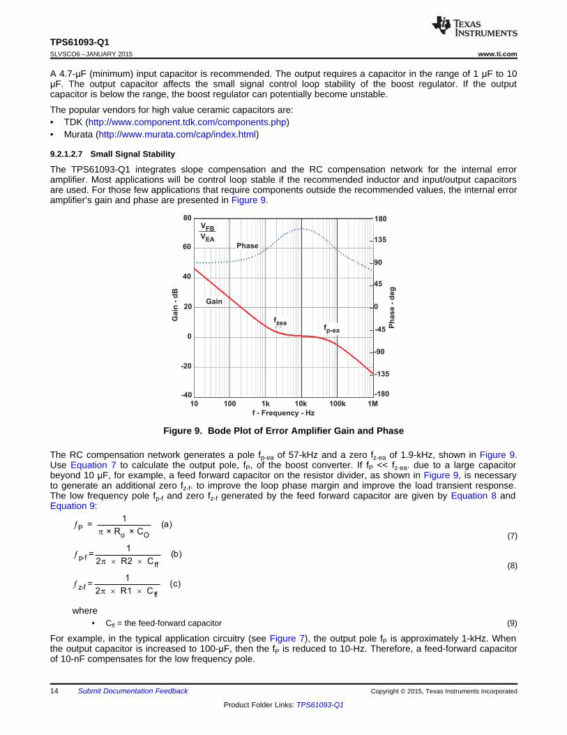
9.2.1.2.7 Small Signal Stability
The TPS61093-Q1 integrates slope compensation and the RC compensation network for the internal erroramplifier. Most applications will be control loop stable if the recommended inductor and input/output capacitorsare used. For those few applications that require components outside the recommended values, the internal erroramplifier’s gain and phase are presented in Figure 9.
Figure 9. Bode Plot of Error Amplifier Gain and Phase
The RC compensation network generates a pole fp-ea of 57-kHz and a zero fz-ea of 1.9-kHz, shown in Figure 9.Use Equation 7 to calculate the output pole, fP, of the boost converter. If fP << fz-ea. due to a large capacitorbeyond 10 μF, for example, a feed forward capacitor on the resistor divider, as shown in Figure 9, is necessaryto generate an additional zero fz-f. to improve the loop phase margin and improve the load transient response.The low frequency pole fp-f and zero fz-f generated by the feed forward capacitor are given by Equation 8 andEquation 9:
(7)
(8)
where• Cff = the feed-forward capacitor (9)
For example, in the typical application circuitry (see Figure 7), the output pole fP is approximately 1-kHz. Whenthe output capacitor is increased to 100-μF, then the fP is reduced to 10-Hz. Therefore, a feed-forward capacitorof 10-nF compensates for the low frequency pole.
14 Submit Documentation Feedback Copyright © 2015, Texas Instruments Incorporated
Product Folder Links: TPS61093-Q1

OUT
100 mV/div; AC
Inductor Current
20 mA/div
t - Time = 1 ms/div
SW
10 V/div VO
5 V/divInductor Current
100 mA/div
t - Time = 40 ms/div
OUT
5 V/div
OUT
100 mV/div; AC
Inductor Current
200 mA/div
t - Time = 400 ns/div
SW
10 V/div
OUT
50 mV/div; AC
Inductor Current
100 mA/div
t - Time = 200 ns/div
SW
10 V/div
OUT
500 mV/div; AC
Inductor Current
200 mA/div
t - Time = 1 ms/div
OUT with Cff
500 mV/div; AC
Load
20 mA/div
t - Time = 1 ms/div
OUT without Cff
500 mV/div; AC
TPS61093-Q1www.ti.com SLVSCO6 –JANUARY 2015
A feed forward capacitor that sets fz-f near 10-kHz improves the load transient response in most applications, asshown in Figure 11.
9.2.1.3 Application Curves
Figure 11. 10mA to 50mA Load Transient ResponseFigure 10. 3.3V to 3.6V Line Transient Response
Figure 13. PWM Control in DCMFigure 12. PWM Control in CCM
Figure 14. Pulse Skip Mode at Light Load Figure 15. Soft Start-Up
Copyright © 2015, Texas Instruments Incorporated Submit Documentation Feedback 15
Product Folder Links: TPS61093-Q1
+10V OUTPUT
5V/DIV
-10V OUTPUT
5V/DIV
Inductor Current
500mA/DIV
t - Time = 40 ms/div
C4
0.1 Fm
BAT54S
-10V/50mA
C6
4.7 Fm
R1
190kW
10V/50mA
TPS61093
CP1
CP2
SW
FBEN
OUT
VO
VIN
GNDSS
C1
4.7 Fm
R2
10.2kW
L1
10 Hm
V 3.3Vin
R3
200kW
C5
1 Fm
C3 100nF
C2
4.7 Fm
TPS61093-Q1SLVSCO6 –JANUARY 2015 www.ti.com
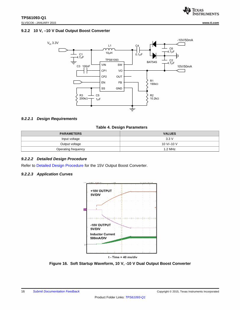
9.2.2 10 V, –10 V Dual Output Boost Converter
9.2.2.1 Design Requirements
Table 4. Design ParametersPARAMETERS VALUES
Input voltage 3.3 VOutput voltage 10 V/–10 V
Operating frequency 1.2 MHz
9.2.2.2 Detailed Design ProcedureRefer to Detailed Design Procedure for the 15V Output Boost Converter.
9.2.2.3 Application Curves
Figure 16. Soft Startup Waveform, 10 V, -10 V Dual Output Boost Converter
16 Submit Documentation Feedback Copyright © 2015, Texas Instruments Incorporated
Product Folder Links: TPS61093-Q1
FB
VO
SW
OUT
SS
CP1
GND
VIN
EN
Therm
alP
ad
CP2
Vout
C1
R1
R2
C3
C2
L1
Vin
R3
GND
C4
C5
Place enough
VIAs around
thermal pad to
enhace thermal
performance
Minimize the
area of SW
trace
TPS61093-Q1www.ti.com SLVSCO6 –JANUARY 2015
10 Power Supply RecommendationsThe device is designed to operate from an input voltage supply range between 1.6 V to 6 V. The input powersupply’s output current needs to be rated according to the supply voltage, output voltage and output current ofthe TPS61093-Q1.
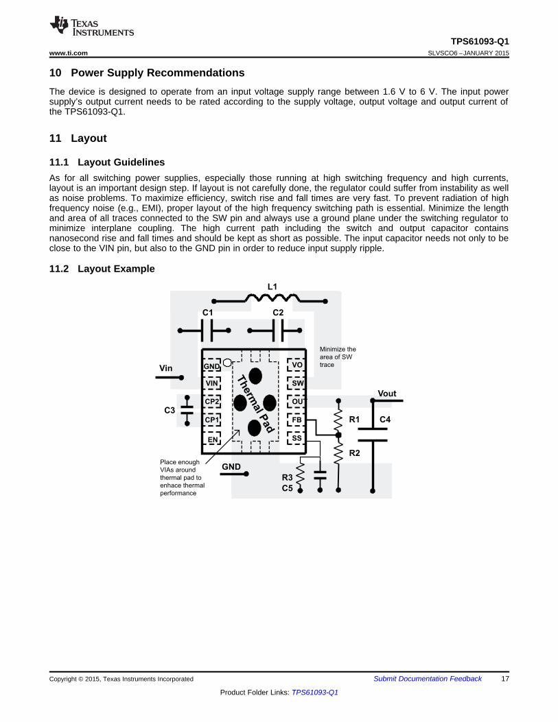
11 Layout
11.1 Layout GuidelinesAs for all switching power supplies, especially those running at high switching frequency and high currents,layout is an important design step. If layout is not carefully done, the regulator could suffer from instability as wellas noise problems. To maximize efficiency, switch rise and fall times are very fast. To prevent radiation of highfrequency noise (e.g., EMI), proper layout of the high frequency switching path is essential. Minimize the lengthand area of all traces connected to the SW pin and always use a ground plane under the switching regulator tominimize interplane coupling. The high current path including the switch and output capacitor containsnanosecond rise and fall times and should be kept as short as possible. The input capacitor needs not only to beclose to the VIN pin, but also to the GND pin in order to reduce input supply ripple.
11.2 Layout Example
Copyright © 2015, Texas Instruments Incorporated Submit Documentation Feedback 17
Product Folder Links: TPS61093-Q1

AD(max)
JA
125 C TP =
Rq
° -
TPS61093-Q1SLVSCO6 –JANUARY 2015 www.ti.com
11.3 Thermal ConsiderationsThe maximum IC junction temperature should be restricted to 125°C under normal operating conditions. Thisrestriction limits the power dissipation of the TPS61093-Q1. Calculate the maximum allowable dissipation,PD(max), and keep the actual dissipation less than or equal to PD(max). The maximum-power-dissipation limit isdetermined using the following equation:
where• TA is the maximum ambient temperature for the application• RθJA is the thermal resistance junction-toambient given in Power Dissipation Table (10)
The TPS61093-Q1 comes in a thermally enhanced SON package. This package includes a thermal pad thatimproves the thermal capabilities of the package. The RθJA of the SON package greatly depends on the PCBlayout and thermal pad connection. The thermal pad must be soldered to the analog ground on the PCB. Usingthermal vias underneath the thermal pad.
18 Submit Documentation Feedback Copyright © 2015, Texas Instruments Incorporated
Product Folder Links: TPS61093-Q1

TPS61093-Q1www.ti.com SLVSCO6 –JANUARY 2015
12 Device and Documentation Support
12.1 TrademarksAll trademarks are the property of their respective owners.
12.2 Electrostatic Discharge CautionThis integrated circuit can be damaged by ESD. Texas Instruments recommends that all integrated circuits be handled withappropriate precautions. Failure to observe proper handling and installation procedures can cause damage.
ESD damage can range from subtle performance degradation to complete device failure. Precision integrated circuits may be moresusceptible to damage because very small parametric changes could cause the device not to meet its published specifications.
12.3 GlossarySLYZ022 — TI Glossary.
This glossary lists and explains terms, acronyms, and definitions.
13 Mechanical, Packaging, and Orderable Information
The following pages include mechanical packaging and orderable information. This information is the mostcurrent data available for the designated devices. This data is subject to change without notice and revision ofthis document. For browser-based versions of this data sheet, refer to the left-hand navigation.
Copyright © 2015, Texas Instruments Incorporated Submit Documentation Feedback 19
Product Folder Links: TPS61093-Q1

PACKAGE OPTION ADDENDUM
www.ti.com 17-Mar-2017
Addendum-Page 1
PACKAGING INFORMATION
Orderable Device Status(1)
Package Type PackageDrawing
Pins PackageQty
Eco Plan(2)
Lead/Ball Finish(6)
MSL Peak Temp(3)
Op Temp (°C) Device Marking(4/5)
Samples
TPS61093QDSKRQ1 ACTIVE SON DSK 10 3000 Green (RoHS& no Sb/Br)
CU NIPDAU Level-1-260C-UNLIM -40 to 125 093Q
(1) The marketing status values are defined as follows:ACTIVE: Product device recommended for new designs.LIFEBUY: TI has announced that the device will be discontinued, and a lifetime-buy period is in effect.NRND: Not recommended for new designs. Device is in production to support existing customers, but TI does not recommend using this part in a new design.PREVIEW: Device has been announced but is not in production. Samples may or may not be available.OBSOLETE: TI has discontinued the production of the device.
(2) Eco Plan - The planned eco-friendly classification: Pb-Free (RoHS), Pb-Free (RoHS Exempt), or Green (RoHS & no Sb/Br) - please check http://www.ti.com/productcontent for the latest availabilityinformation and additional product content details.TBD: The Pb-Free/Green conversion plan has not been defined.Pb-Free (RoHS): TI's terms "Lead-Free" or "Pb-Free" mean semiconductor products that are compatible with the current RoHS requirements for all 6 substances, including the requirement thatlead not exceed 0.1% by weight in homogeneous materials. Where designed to be soldered at high temperatures, TI Pb-Free products are suitable for use in specified lead-free processes.Pb-Free (RoHS Exempt): This component has a RoHS exemption for either 1) lead-based flip-chip solder bumps used between the die and package, or 2) lead-based die adhesive used betweenthe die and leadframe. The component is otherwise considered Pb-Free (RoHS compatible) as defined above.Green (RoHS & no Sb/Br): TI defines "Green" to mean Pb-Free (RoHS compatible), and free of Bromine (Br) and Antimony (Sb) based flame retardants (Br or Sb do not exceed 0.1% by weightin homogeneous material)
(3) MSL, Peak Temp. - The Moisture Sensitivity Level rating according to the JEDEC industry standard classifications, and peak solder temperature.
(4) There may be additional marking, which relates to the logo, the lot trace code information, or the environmental category on the device.
(5) Multiple Device Markings will be inside parentheses. Only one Device Marking contained in parentheses and separated by a "~" will appear on a device. If a line is indented then it is a continuationof the previous line and the two combined represent the entire Device Marking for that device.
(6) Lead/Ball Finish - Orderable Devices may have multiple material finish options. Finish options are separated by a vertical ruled line. Lead/Ball Finish values may wrap to two lines if the finishvalue exceeds the maximum column width.
Important Information and Disclaimer:The information provided on this page represents TI's knowledge and belief as of the date that it is provided. TI bases its knowledge and belief on informationprovided by third parties, and makes no representation or warranty as to the accuracy of such information. Efforts are underway to better integrate information from third parties. TI has taken andcontinues to take reasonable steps to provide representative and accurate information but may not have conducted destructive testing or chemical analysis on incoming materials and chemicals.TI and TI suppliers consider certain information to be proprietary, and thus CAS numbers and other limited information may not be available for release.
In no event shall TI's liability arising out of such information exceed the total purchase price of the TI part(s) at issue in this document sold by TI to Customer on an annual basis.

PACKAGE OPTION ADDENDUM
www.ti.com 17-Mar-2017
Addendum-Page 2
OTHER QUALIFIED VERSIONS OF TPS61093-Q1 :
• Catalog: TPS61093
NOTE: Qualified Version Definitions:
• Catalog - TI's standard catalog product

TAPE AND REEL INFORMATION
*All dimensions are nominal
Device PackageType
PackageDrawing
Pins SPQ ReelDiameter
(mm)
ReelWidth
W1 (mm)
A0(mm)
B0(mm)
K0(mm)
P1(mm)
W(mm)
Pin1Quadrant
TPS61093QDSKRQ1 SON DSK 10 3000 180.0 8.4 2.8 2.8 1.0 4.0 8.0 Q2
PACKAGE MATERIALS INFORMATION
www.ti.com 16-Feb-2015
Pack Materials-Page 1

*All dimensions are nominal
Device Package Type Package Drawing Pins SPQ Length (mm) Width (mm) Height (mm)
TPS61093QDSKRQ1 SON DSK 10 3000 210.0 185.0 35.0
PACKAGE MATERIALS INFORMATION
www.ti.com 16-Feb-2015
Pack Materials-Page 2


IMPORTANT NOTICE
Texas Instruments Incorporated (TI) reserves the right to make corrections, enhancements, improvements and other changes to itssemiconductor products and services per JESD46, latest issue, and to discontinue any product or service per JESD48, latest issue. Buyersshould obtain the latest relevant information before placing orders and should verify that such information is current and complete.TI’s published terms of sale for semiconductor products (http://www.ti.com/sc/docs/stdterms.htm) apply to the sale of packaged integratedcircuit products that TI has qualified and released to market. Additional terms may apply to the use or sale of other types of TI products andservices.Reproduction of significant portions of TI information in TI data sheets is permissible only if reproduction is without alteration and isaccompanied by all associated warranties, conditions, limitations, and notices. TI is not responsible or liable for such reproduceddocumentation. Information of third parties may be subject to additional restrictions. Resale of TI products or services with statementsdifferent from or beyond the parameters stated by TI for that product or service voids all express and any implied warranties for theassociated TI product or service and is an unfair and deceptive business practice. TI is not responsible or liable for any such statements.Buyers and others who are developing systems that incorporate TI products (collectively, “Designers”) understand and agree that Designersremain responsible for using their independent analysis, evaluation and judgment in designing their applications and that Designers havefull and exclusive responsibility to assure the safety of Designers' applications and compliance of their applications (and of all TI productsused in or for Designers’ applications) with all applicable regulations, laws and other applicable requirements. Designer represents that, withrespect to their applications, Designer has all the necessary expertise to create and implement safeguards that (1) anticipate dangerousconsequences of failures, (2) monitor failures and their consequences, and (3) lessen the likelihood of failures that might cause harm andtake appropriate actions. Designer agrees that prior to using or distributing any applications that include TI products, Designer willthoroughly test such applications and the functionality of such TI products as used in such applications.TI’s provision of technical, application or other design advice, quality characterization, reliability data or other services or information,including, but not limited to, reference designs and materials relating to evaluation modules, (collectively, “TI Resources”) are intended toassist designers who are developing applications that incorporate TI products; by downloading, accessing or using TI Resources in anyway, Designer (individually or, if Designer is acting on behalf of a company, Designer’s company) agrees to use any particular TI Resourcesolely for this purpose and subject to the terms of this Notice.TI’s provision of TI Resources does not expand or otherwise alter TI’s applicable published warranties or warranty disclaimers for TIproducts, and no additional obligations or liabilities arise from TI providing such TI Resources. TI reserves the right to make corrections,enhancements, improvements and other changes to its TI Resources. TI has not conducted any testing other than that specificallydescribed in the published documentation for a particular TI Resource.Designer is authorized to use, copy and modify any individual TI Resource only in connection with the development of applications thatinclude the TI product(s) identified in such TI Resource. NO OTHER LICENSE, EXPRESS OR IMPLIED, BY ESTOPPEL OR OTHERWISETO ANY OTHER TI INTELLECTUAL PROPERTY RIGHT, AND NO LICENSE TO ANY TECHNOLOGY OR INTELLECTUAL PROPERTYRIGHT OF TI OR ANY THIRD PARTY IS GRANTED HEREIN, including but not limited to any patent right, copyright, mask work right, orother intellectual property right relating to any combination, machine, or process in which TI products or services are used. Informationregarding or referencing third-party products or services does not constitute a license to use such products or services, or a warranty orendorsement thereof. Use of TI Resources may require a license from a third party under the patents or other intellectual property of thethird party, or a license from TI under the patents or other intellectual property of TI.TI RESOURCES ARE PROVIDED “AS IS” AND WITH ALL FAULTS. TI DISCLAIMS ALL OTHER WARRANTIES ORREPRESENTATIONS, EXPRESS OR IMPLIED, REGARDING RESOURCES OR USE THEREOF, INCLUDING BUT NOT LIMITED TOACCURACY OR COMPLETENESS, TITLE, ANY EPIDEMIC FAILURE WARRANTY AND ANY IMPLIED WARRANTIES OFMERCHANTABILITY, FITNESS FOR A PARTICULAR PURPOSE, AND NON-INFRINGEMENT OF ANY THIRD PARTY INTELLECTUALPROPERTY RIGHTS. TI SHALL NOT BE LIABLE FOR AND SHALL NOT DEFEND OR INDEMNIFY DESIGNER AGAINST ANY CLAIM,INCLUDING BUT NOT LIMITED TO ANY INFRINGEMENT CLAIM THAT RELATES TO OR IS BASED ON ANY COMBINATION OFPRODUCTS EVEN IF DESCRIBED IN TI RESOURCES OR OTHERWISE. IN NO EVENT SHALL TI BE LIABLE FOR ANY ACTUAL,DIRECT, SPECIAL, COLLATERAL, INDIRECT, PUNITIVE, INCIDENTAL, CONSEQUENTIAL OR EXEMPLARY DAMAGES INCONNECTION WITH OR ARISING OUT OF TI RESOURCES OR USE THEREOF, AND REGARDLESS OF WHETHER TI HAS BEENADVISED OF THE POSSIBILITY OF SUCH DAMAGES.Unless TI has explicitly designated an individual product as meeting the requirements of a particular industry standard (e.g., ISO/TS 16949and ISO 26262), TI is not responsible for any failure to meet such industry standard requirements.Where TI specifically promotes products as facilitating functional safety or as compliant with industry functional safety standards, suchproducts are intended to help enable customers to design and create their own applications that meet applicable functional safety standardsand requirements. Using products in an application does not by itself establish any safety features in the application. Designers mustensure compliance with safety-related requirements and standards applicable to their applications. Designer may not use any TI products inlife-critical medical equipment unless authorized officers of the parties have executed a special contract specifically governing such use.Life-critical medical equipment is medical equipment where failure of such equipment would cause serious bodily injury or death (e.g., lifesupport, pacemakers, defibrillators, heart pumps, neurostimulators, and implantables). Such equipment includes, without limitation, allmedical devices identified by the U.S. Food and Drug Administration as Class III devices and equivalent classifications outside the U.S.TI may expressly designate certain products as completing a particular qualification (e.g., Q100, Military Grade, or Enhanced Product).Designers agree that it has the necessary expertise to select the product with the appropriate qualification designation for their applicationsand that proper product selection is at Designers’ own risk. Designers are solely responsible for compliance with all legal and regulatoryrequirements in connection with such selection.Designer will fully indemnify TI and its representatives against any damages, costs, losses, and/or liabilities arising out of Designer’s non-compliance with the terms and provisions of this Notice.
Mailing Address: Texas Instruments, Post Office Box 655303, Dallas, Texas 75265Copyright © 2017, Texas Instruments Incorporated
Related Documents


