I J C T A, 8(2), 2015, pp. 505-512 © International Science Press * Assistant Professor, PSN College of Engineering and Technology, India ** Assistant Professor, PSN College of Engineering and Technology and Research Scholar, Sathyabama University, India Low Area Wallace Multiplier Using Energy Efficient CMOS Adder Circuit Analysis In Instrumentation G. Sridhar * and T. Reenaraj ** Abstract: In most digital and high performance systems such as Microprocessor,FIR filter and Digital Signal Processor,Multiplier plays an important role.In this paper,the multiplier offers less area and power consumption is reduced. To reduce the hardware component, Energy efficient CMOS full adder plays an important role in Wallace tree multiplier.Modified Wallace multiplier have minimum adders than Standard Wallace Multiplier.In this paper,the energy efficient CMOS full adder is used in the modified Wallace multiplier at the place of full adder in the standard Wallace multiplier in order to reduce area and power consumption. Keywords: Energy efficient full adder, CMOS full adder, Wallace multiplier. 1. INTRODUCTION VLSI stands for “Very Large Scale Integration”. This is the field which involves packing more and more logic devices into small areas. Alongside, obeying Moore’s law, the capability of an IC has increased exponentially over the years, in terms of computation of power, utilization of available area, yield. The combined effect of these two advances is that people can now put diverse functionality into the IC’s, opening up new frontiers. Examples are embedded systems, where intelligent devices are put inside everyday objects, and ubiquitous computing where small computing devices proliferate to such an extent that even the shoes you wear may actually do something useful like monitoring your heartbeats. The increasing prominence of portable systems and the need to limit power consumption (and hence, heat dissipation) in very-high density VLSI chips have led to rapid and innovative developments in low- power design during the recent years. The ever increasing demand for portable computing devices and wireless communication systems require low power VLSI circuits. Minimizing power dissipation during the VLSI design flow increases life time and reliability of the circuit. Numerous techniques for the design of low power VLSI circuits are reported where the dominant factor of power dissipation is caused by switching activity. While these techniques have reduced the circuit power dissipation during functional operation, testing of such low power VLSI circuits has recently become an area of concern. Therefore addressing the problems associated with testing low power VLSI circuits have become an important issue. Challenges As microprocessors become more complex due to technology scaling, microprocessor designers have encountered several challenges which force them to think beyond the design plane, and look ahead to post- silicon: • Process variation – As photolithography techniques tend closer to the fundamental laws of optics, achieving high accuracy in doping concentrations and etched wires is becoming more difficult and

Welcome message from author
This document is posted to help you gain knowledge. Please leave a comment to let me know what you think about it! Share it to your friends and learn new things together.
Transcript

I J C T A, 8(2), 2015, pp. 505-512© International Science Press
* Assistant Professor, PSN College of Engineering and Technology, India** Assistant Professor, PSN College of Engineering and Technology and Research Scholar, Sathyabama University, India
Low Area Wallace Multiplier Using EnergyEfficient CMOS Adder Circuit Analysis InInstrumentationG. Sridhar* and T. Reenaraj**
Abstract: In most digital and high performance systems such as Microprocessor,FIR filter and Digital SignalProcessor,Multiplier plays an important role.In this paper,the multiplier offers less area and power consumption isreduced. To reduce the hardware component, Energy efficient CMOS full adder plays an important role in Wallacetree multiplier.Modified Wallace multiplier have minimum adders than Standard Wallace Multiplier.In this paper,theenergy efficient CMOS full adder is used in the modified Wallace multiplier at the place of full adder in thestandard Wallace multiplier in order to reduce area and power consumption.
Keywords: Energy efficient full adder, CMOS full adder, Wallace multiplier.
1. INTRODUCTION
VLSI stands for “Very Large Scale Integration”. This is the field which involves packing more and morelogic devices into small areas. Alongside, obeying Moore’s law, the capability of an IC has increasedexponentially over the years, in terms of computation of power, utilization of available area, yield. Thecombined effect of these two advances is that people can now put diverse functionality into the IC’s,opening up new frontiers. Examples are embedded systems, where intelligent devices are put inside everydayobjects, and ubiquitous computing where small computing devices proliferate to such an extent that eventhe shoes you wear may actually do something useful like monitoring your heartbeats.
The increasing prominence of portable systems and the need to limit power consumption (and hence,heat dissipation) in very-high density VLSI chips have led to rapid and innovative developments in low-power design during the recent years. The ever increasing demand for portable computing devices andwireless communication systems require low power VLSI circuits. Minimizing power dissipation duringthe VLSI design flow increases life time and reliability of the circuit. Numerous techniques for the designof low power VLSI circuits are reported where the dominant factor of power dissipation is caused byswitching activity. While these techniques have reduced the circuit power dissipation during functionaloperation, testing of such low power VLSI circuits has recently become an area of concern. Thereforeaddressing the problems associated with testing low power VLSI circuits have become an important issue.
Challenges
As microprocessors become more complex due to technology scaling, microprocessor designers haveencountered several challenges which force them to think beyond the design plane, and look ahead to post-silicon:
• Process variation – As photolithography techniques tend closer to the fundamental laws of optics,achieving high accuracy in doping concentrations and etched wires is becoming more difficult and

506 G. Sridhar and T. Reenaraj
prone to errors due to variation. Designers now must simulate across multiple fabrication processcorners before a chip is certified ready for production.
• Stricter design rules – Due to lithography and etch issues with scaling, design rules for layout havebecome increasingly stringent. Designers must keep ever more of these rules in mind while layingout custom circuits. The overhead for custom design is now reaching a tip point, with many designhouses opting to switch to electronic design automation (EDA) tools to automate their design process.
• Timing/design closure – As clock frequencies tend to scale up, designers are finding it more difficultto distribute and maintain low clock skew between these high frequency clocks across the entirechip. This has led to a rising interest in multicore and multiprocessor architectures, since an overallspeedup can be obtained by lowering the clock frequency and distributing processing.
• First-pass success – As die sizes shrink (due to scaling), and wafer sizes go up (to lowermanufacturing costs), the number of dies per wafer increases, and the complexity of making suitablephotomasks goes up rapidly. A mask set for a modern technology can cost several million dollars.This non-recurring expense deters the old iterative philosophy involving several “spin-cycles” tofind errors in silicon, and encourages first-pass silicon success. Several design philosophies havebeen developed to aid this new design flow, including design for manufacturing (DFM), design fortest (DFT), and Design for X.
2. OBJECTIVE OF THE WORK
A Wallace tree is an efficient hardware implementation of a digital circuit that multiplies two integers.Theentire procedure is carried out into three steps:
• Partial product generation,
• Partial product grouping and reduction,
• Final adding.
The main objective of this project :
• To reduce area : The area can be reduced by minimizing gate counts in adder using commonboolean logic.
• To reduce power consumption: The lower power consumption will be achieved by minimizingthe area.
PROJECT DESCRIPTION
Wallace Tree Multiplier
A Wallace tree is an efficient hardware implementation of a digital circuit that multiplies two integers,devised by an Australian Computer Scientist Chris Wallace in 1964.
Figure 3.1: Basic Wallace Tree

Low Area Wallace Multiplier using Energy Efficient CMOS Adder Circuit Analysis in Instrumentation 507
The Wallace tree has three steps:
1. Multiply (that is - AND) each bit of one of the arguments, by each bit of the other, yielding n2
results. Depending on position of the multiplied bits, the wires carry different weights, for examplewire of bit carrying result of a
2 b
3 is 32 (see explanation of weights below).
2. Reduce the number of partial products to two by layers of full and half adders.
3. Group the wires in two numbers, and add them with a conventional adder.
The Wallace tree multiplier is considerably faster than a simple array multiplier because its height islogarithmic in word size, not linear. However, in addition to the large number of adders required, theWallace tree’s wiring is much less regular and more complicated. As a result, Wallace trees are oftenavoided by designers, while design complexityis a concern to them. Wallace tree styles use a log-depthtreenetwork for reduction. Faster, but irregular, they trade ease of layout for speed. Wallace tree styles aregenerally avoided for low power applications, since excess of wiring is likely to consume extra power.While subsequently faster than Carry-save structure for large bit multipliers, the Wallace tree multiplier hasthe disadvantage of being very irregular, which complicates the task of coming with an efficient layout. TheWallace tree multiplier is a high speed multiplier. The summing of the partial product bits in parallel usinga tree of carry-save adders became generally known as the “Wallace Tree”. Three step processes are usedto multiply two numbers.
• Formation of bit products.
• Reduction of the bit product matrix into a two row matrix by means of a carry save adder.
• Summation of remaining two rows using a faster Carry Look Ahead Adder (CLA).
Figure 3.2: Flow diagram of Wallace tree Figure 3.3: Wallace Multiplication
The second phase works as follows:
As long as there are three or more wires with the same weight add a following layer:
Take any three wires with the same weights and input them into full adder. The result will be an outputwire of the same weight and an output wire with a higher weight for each three input wires.
• If there are two wires of the same weight left, input them into half adder.
• If there is just one wire left, connect it to the next layer.
The benefit of the Wallace tree is that there are only o(log n) reduction layers, and each layer has o(1)propagation delay. As making the partial products is o(1) and the final addition iso (log n), the multiplicationis only o(log n), not much slower than addition (however, much more expensive in the gate count).Adding
508 G. Sridhar and T. Reenaraj
partial products with regular adders would require o(log2n) time. From a complexity theoretic perspective,the Wallace tree algorithm puts multiplication in the class NC.These computations only consider gatedelays and don’t deal with wire delays, which can also be very substantial. The Wallace tree can be alsorepresented by a tree of 3/2 or 4/2 adders.
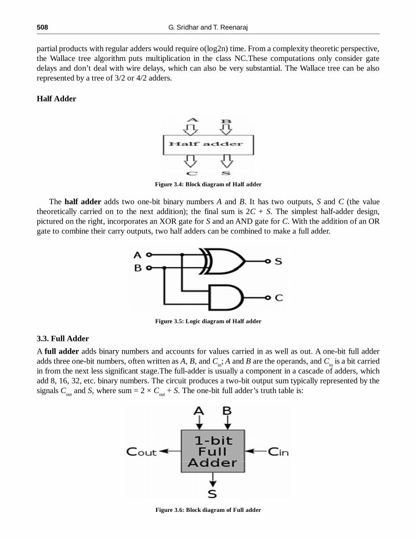
Half Adder
Figure 3.4: Block diagram of Half adder
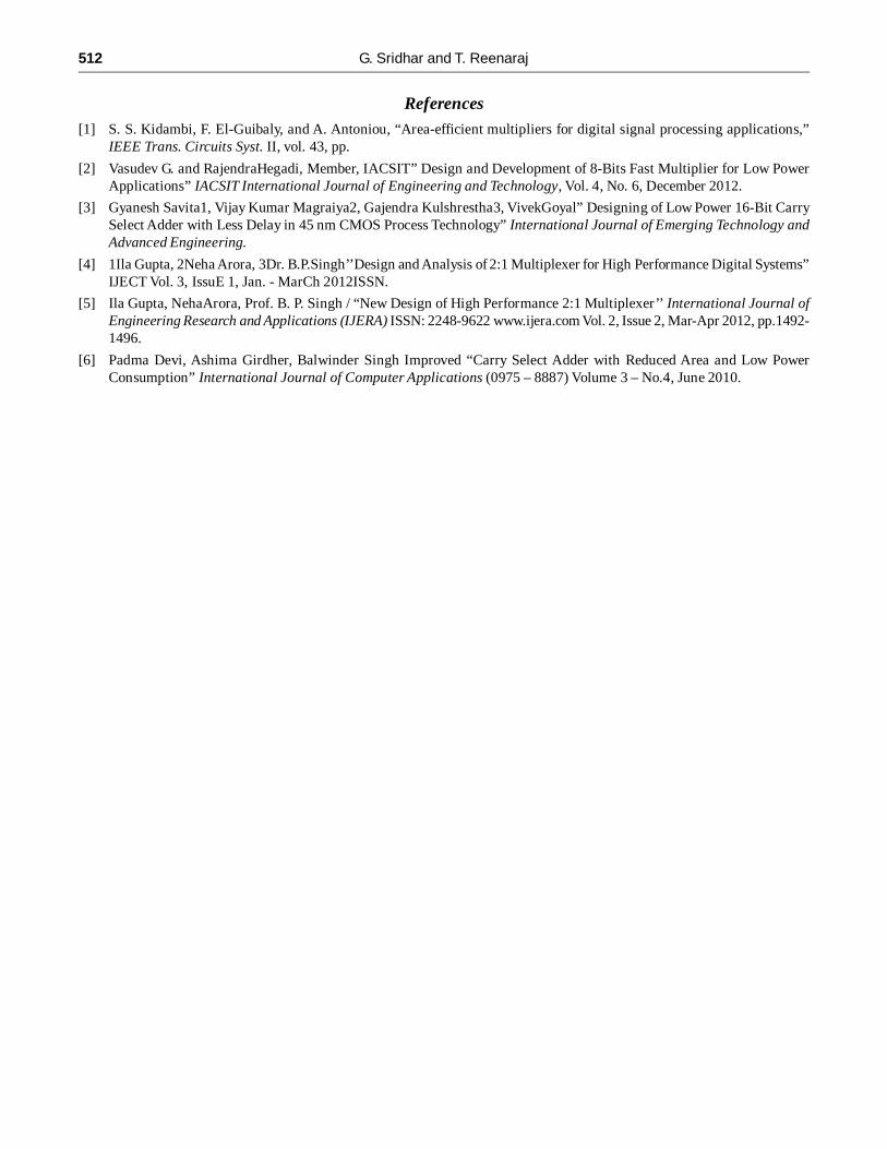
The half adder adds two one-bit binary numbers A and B. It has two outputs, S and C (the valuetheoretically carried on to the next addition); the final sum is 2C + S. The simplest half-adder design,pictured on the right, incorporates an XOR gate for S and an AND gate for C. With the addition of an ORgate to combine their carry outputs, two half adders can be combined to make a full adder.
Figure 3.5: Logic diagram of Half adder
3.3. Full Adder
A full adder adds binary numbers and accounts for values carried in as well as out. A one-bit full adderadds three one-bit numbers, often written as A, B, and C
in; A and B are the operands, and C
in is a bit carried
in from the next less significant stage.The full-adder is usually a component in a cascade of adders, whichadd 8, 16, 32, etc. binary numbers. The circuit produces a two-bit output sum typically represented by thesignals C
out and S, where sum = 2 × C
out + S. The one-bit full adder’s truth table is:
Figure 3.6: Block diagram of Full adder

Low Area Wallace Multiplier using Energy Efficient CMOS Adder Circuit Analysis in Instrumentation 509
A full adder can be implemented in many different ways such as with a custom transistor-level circuitor composed of other gates. One example implementation is with
S = A � B � Cin
Cout
= (A � B) + (Cin � (A � B)).
In this implementation, the final OR gate before the carry-out output may be replaced by an XOR gatewithout altering the resulting logic. Using only two types of gates is convenient if the circuit is beingimplemented using simple IC chips which contain only one gate type per chip. In this light, C
out can be
implemented as
Cout
= (A ��B) � (Cin � (A � B))
A full adder can be constructed from two half adders by connecting A and B to the input of one halfadder, connecting the sum from that to an input to the second adder, connecting C
i to the other input and OR
the two carry outputs. Equivalently, S could be made the three-bit XOR of A, B, and Ci, and C
out could be
made the three-bit majority function of A, B, and Ci.
3. EXISTING WORK
An Existing Full adder design using alternative logic scheme gives low power delay product (PDP), interms of speed, power consumption and reduced Area . Examining the truth table of EFA, it can be seenthat the S0 output gives A XOR B when C=0, and it also gives A XNOR B when C= 1. Thus, the Multiplexercan use to obtain the respective value taking C input as a selection signal. Following the same criteriataking C0 as a output equals to A AND B when input C=0, and A OR B when input C=1. Again C can beused as a respective value for the required result, using Multiplexer. An alternative logic scheme to designa full adder cell can be formed by a logic block to obtain the A XOR B and A XNOR B signals , anotherblock can be obtain the A AND B and A OR B signals, and two Multiplexers driven by the C input togenerate S0 and C0 outputs as shown in fig. Full adder design using swing restore complementary Pass-Transistor logic (SR-CPL) style [4] build the AND/OR gates And XOR/XNOR gates, and multiplexerbased on pass transistor to obtain S0 and C0 output. The AND/OR gates build using a powerless andgroundless pass-transistor logic.
Figure 3.7: Logic diagram of Full adder

510 G. Sridhar and T. Reenaraj
Double-pass transistor logic eliminates some of the inverter stages required for complementary passtransistor logic by using both N and P transistors, with dual logic paths for every function. While it has highspeed due to low input capacitance, it has only limited capacity to drive a load
Drawbacks of Existing Work
• Higher number of great count in full adder circuit
• Higher power consumption
• Low performance
4. PROPOSED WORK
The proposed full adder uses two XOR gates and one 2: 1multiplexer unit. A and B are the inputs of firstXOR gate and produce the output Y. Sum is generated by the XOR operation of Cin as one input and theoutput generated from the previous XOR gate Y is given as the another input . The carry is generated fromthe 2:1 multiplexer unit. The input of the multiplexer is A and Cin. Y acts as the control/selection signal ofmultiplexer. The carry Cout is generated depending upon the control signal.
Figure 3.8: Logic diagram of Existing Full adder

Low Area Wallace Multiplier using Energy Efficient CMOS Adder Circuit Analysis in Instrumentation 511
Advantages of Proposed Work
• Reduce power consumption
• Reduce area
• High performance
5. SIMULATION PROCEDURE
MICROWIND AND DSCH – NOR EXAMPLE
• We will learn both the design flow and the CAD tools.
• The specifications we are going to see may be different for different foundry and technology.
• Design Example (2 Levels) : NOR Gate
� Logic design
� Circuit design
6. DESIGN AND SIMULATION RESULTS
7. CONCLUSION
In this project, the proposed full adder design which consumes less area and power than the existing fulladder. The layout simulation have been done for the proposed circuit in order show the improvement in powerconsumption over supply voltages, operating frequency and temperature. The proposed adder has been designedusing 45nm technology and proved it to be a better option for low power complex system design. The neteffect is that proposed full adder shows a much better performance compared to existing full adder.
8. FUTURE ENHANCEMENT
In future work,the proposed full adder design will be implemented in Wallace multiplier to reduce the gatecount and also to reduce power consumption.
512 G. Sridhar and T. Reenaraj
References[1] S. S. Kidambi, F. El-Guibaly, and A. Antoniou, “Area-efficient multipliers for digital signal processing applications,”
IEEE Trans. Circuits Syst. II, vol. 43, pp.
[2] Vasudev G. and RajendraHegadi, Member, IACSIT” Design and Development of 8-Bits Fast Multiplier for Low PowerApplications” IACSIT International Journal of Engineering and Technology, Vol. 4, No. 6, December 2012.
[3] Gyanesh Savita1, Vijay Kumar Magraiya2, Gajendra Kulshrestha3, VivekGoyal” Designing of Low Power 16-Bit CarrySelect Adder with Less Delay in 45 nm CMOS Process Technology” International Journal of Emerging Technology andAdvanced Engineering.
[4] 1Ila Gupta, 2Neha Arora, 3Dr. B.P.Singh’’Design and Analysis of 2:1 Multiplexer for High Performance Digital Systems”IJECT Vol. 3, IssuE 1, Jan. - MarCh 2012ISSN.
[5] Ila Gupta, NehaArora, Prof. B. P. Singh / “New Design of High Performance 2:1 Multiplexer’’ International Journal ofEngineering Research and Applications (IJERA) ISSN: 2248-9622 www.ijera.com Vol. 2, Issue 2, Mar-Apr 2012, pp.1492-1496.
[6] Padma Devi, Ashima Girdher, Balwinder Singh Improved “Carry Select Adder with Reduced Area and Low PowerConsumption” International Journal of Computer Applications (0975 – 8887) Volume 3 – No.4, June 2010.
Related Documents


![A Low-Power High-speed Pipelined Accumulator Design Using ... · DPL full adder cells ... full adder [5]. The quasi N-P domino FA cell ... A Low-Power High-speed Pipelined Accumulator](https://static.cupdf.com/doc/110x72/5b5b7a557f8b9a2d458dc8b2/a-low-power-high-speed-pipelined-accumulator-design-using-dpl-full-adder.jpg)