University of New Mexico UNM Digital Repository Optical Science and Engineering ETDs Engineering ETDs 6-28-2010 Longwave and bi-color type-II InAs/(In)GaSb superlaice infrared detectors Arezou Khoshakhlagh Follow this and additional works at: hps://digitalrepository.unm.edu/ose_etds is Dissertation is brought to you for free and open access by the Engineering ETDs at UNM Digital Repository. It has been accepted for inclusion in Optical Science and Engineering ETDs by an authorized administrator of UNM Digital Repository. For more information, please contact [email protected]. Recommended Citation Khoshakhlagh, Arezou. "Longwave and bi-color type-II InAs/(In)GaSb superlaice infrared detectors." (2010). hps://digitalrepository.unm.edu/ose_etds/12

Welcome message from author
This document is posted to help you gain knowledge. Please leave a comment to let me know what you think about it! Share it to your friends and learn new things together.
Transcript

University of New MexicoUNM Digital Repository
Optical Science and Engineering ETDs Engineering ETDs
6-28-2010
Longwave and bi-color type-II InAs/(In)GaSbsuperlattice infrared detectorsArezou Khoshakhlagh
Follow this and additional works at: https://digitalrepository.unm.edu/ose_etds
This Dissertation is brought to you for free and open access by the Engineering ETDs at UNM Digital Repository. It has been accepted for inclusion inOptical Science and Engineering ETDs by an authorized administrator of UNM Digital Repository. For more information, please [email protected].
Recommended CitationKhoshakhlagh, Arezou. "Longwave and bi-color type-II InAs/(In)GaSb superlattice infrared detectors." (2010).https://digitalrepository.unm.edu/ose_etds/12

Longwave and Bi-color Type-II
InAs/(In)GaSb Superlattice Infrared Detectors
by
Arezou Khoshakhlagh
B.S., University of New Mexico, 2004 M.S., University of New Mexico, 2008
DISSERTATION
Submitted in Partial Fulfillment of the Requirements for the Degree of
Doctor of Philosophy
Optical Sciences and Engineering
The University of New Mexico Albuquerque, New Mexico
May, 2010

c©2010, Arezou Khoshakhlagh
iii

Dedication
To my Parents,
Shahnaz and Rahman
iv

Acknowledgments
First and foremost I offer my sincerest gratitude to my advisor, Dr. Sanjay Krishna,
who has supported me throughout my thesis with his patience and knowledge whilst
allowing me the room to work in my own way. I attribute this thesis to his encour-
agement and effort and without his support this thesis, too, would not have been
completed or written. One simply could not wish for a better or friendlier advisor.
I greatly acknowledge the assistance provided to me by the members of my disser-
tation committee, Dr. Ralph Dawson, Dr. Luke Lester and Dr. Abhaya Datye. I
sincerely appreciate the crystal growth knowledge bestowed upon me by Dr. Ralph
Dawson. I would also like to acknowledge the group members for their support and
great teamwork: Dr. J.B. Rodriguez, Dr. Elena Plis, Hasul Kim, Stephen Myers,
Nutan Gautam, and Brianna Klein.
I would like to thank my family and friends for their support. My special thanks
goes to my parents, Rahman and Shahnaz and my husband, Mahmood. Without
their love, support and understanding I would not have been able to finish this thesis.
v

Longwave and Bi-color Type-II
InAs/(In)GaSb Supperlattice Infrared Detectors
BY
Arezou Khoshakhlagh
ABSTRACT OF DISSERTATION
Submitted in Partial Fulfillment of the Requirements for the Degree of
Doctor of Philosophy
Optical Sciences and Engineering
The University of New Mexico Albuquerque, New Mexico
May, 2010

Longwave and Bi-color Type-IIInAs/(In)GaSb Superlattice Infrared
Detectors
by
Arezou Khoshakhlagh
B.S., University of New Mexico, 2004
M.S., University of New Mexico, 2008
Ph.D., Optical Sciences and Engineering, University of New Mexico,
2010
Abstract
Infrared (IR) photodetectors are useful for a variety of military and civil applications
such as target acquisition, medical diagnostics, pollution monitoring, to name just
a few. Presently photonic IR detectors are based on interband transitions in low
bandgap semiconductors such as mercury cadmium telluride (MCT) or InSb or in
intersubband transitions in hetero-engineered structures such as quantum well or
quantum dot infrared photodetectors (QWIPs or QDIPs). These detectors operate
at low temperatures (77 K-200 K) in order to obtain high signal to noise ratio.
The cooling requirement limits the lifetime, increases the weight and the total cost,
as well as the power budget, of the whole infrared system. There is a concerted
effort to develop photonic detectors operating at higher temperatures. In the past
few years, interband transitions in type II InAs/GaSb strain layer superlattices (SL)
vii
have emerged as a competing technology among other IR systems. Although MCT
and QWIP technologies are relatively more mature than the SL technology, the SL
technology has potential to enhance performance in several key areas. One of the
main advantages of this system lies in the fact that the effective band gap of the SL
can be tailored over a wide range (3 µm < λc < 30 µm) by varying the thickness of two
“mid bandgap” constituent materials, namely GaSb and InAs. Tunneling currents
in SL are reduced due to a larger electron effective mass. Large splitting between
heavy-hole and light-hole valence subbands due to strain in the SLs contributes to
the suppression of Auger recombination. Moreover, the band structure of the SL can
be engineered to enhance carrier lifetimes and reduce noise at higher temperatures.
SL based IR detectors have demonstrated high quantum efficiency, high temperature
operation, and are suitable for incorporation in focal plane arrays (FPA) by tapping
into the mature III-V based growth and fabrication processes.
The recently proposed nBn heterostructure design has demonstrated a 100 K in-
crease in background-limited infrared photodetection (BLIP) for InAs-based device,
by decreasing Shockley-Read-Hall generation currents and by suppressing surface
currents using specific processing.
Third generation IR detectors have three main emphasis, High operating temper-
ature (HOT), multicolor capability, and large format arrays. This work concentrates
on multicolor and HOT IR detectors based on nBn design. Contributions of this
thesis include
1. Development of design and growth procedure for the long-wave (LW)
SL detectors leading to an improved detector performance
13 MLs of InAs and 7 MLs of GaSb with InSb strain compensating layer were
designed and optimized for LW SL detectors. LWIR pin and nBn detectors
were introduced and their optical and electrical properties were compared. LW
viii
nBn detectors show higher device performance in terms of lower dark current
density and higher responsivity as compared to the LW pin detectors. The
reduction in dark current in LW nBn detector is due to reduction of SRH
centers as well as surface leakage currents. The increase in responsivity for LW
nBn detectors is due to reduction non-radiative SRH recombination.
2. Design, growth and characterization of bi-color nBn detectors
Present day two color SL detectors require two contacts per pixel leading to
a complicated processing scheme and expensive read out integrated circuits
(ROICs). The nBn architecture was modified to realize a dual-band response
by changing the polarity of applied bias using single contact processing. The
spectral response shows a significant change in the LWIR to MWIR ratio within
a very small bias range (∼100 mV ) making it compatible with commercially
available ROICs.
3. Investigation of background carrier concentration in SLs
The electrical transport in SLs was investigated in order to improve the collec-
tion efficiency and understand SL devices performance operating at ambient
temperature. For this purpose background carrier concentration of type-II
InAs/GaSb SLs on GaAs substrates are studied. The hall measurements on
mid-wave SLs revealed that the conduction in the MWIR SLs is dominated by
holes at low temperatures (< 200 K) and by electrons at high temperatures
(> 200 K) and is dominated by electrons at all temperatures for LWIR SLs
possibly due to the thicker InAs (residually n-type) and thinner GaSb (resid-
ually p-type) layers. By studying the in-plane transport characteristics of LW
SLs grown at different temperatures, it was shown that interface roughness
scattering is the dominant scattering mechanism at higher temperatures (200
K- 300 K).
ix

Contents
List of Figures xv
List of Tables xxii
1 Introduction 1
1.1 Basics of infrared detection . . . . . . . . . . . . . . . . . . . . . . . . 1
1.1.1 Thermal Radiation Laws . . . . . . . . . . . . . . . . . . . . . 3
1.2 Infrared detectors . . . . . . . . . . . . . . . . . . . . . . . . . . . . . 5
1.2.1 Thermal Detectors . . . . . . . . . . . . . . . . . . . . . . . . 5
1.2.2 Photon detectors . . . . . . . . . . . . . . . . . . . . . . . . . 6
1.3 Figures of merit for infrared detectors . . . . . . . . . . . . . . . . . . 8
1.3.1 Responsivity . . . . . . . . . . . . . . . . . . . . . . . . . . . . 9
1.3.2 Noise Equivalent Power . . . . . . . . . . . . . . . . . . . . . . 10
1.3.3 Detectivity . . . . . . . . . . . . . . . . . . . . . . . . . . . . 10
1.4 Focal Plane Arrays (FPAs) . . . . . . . . . . . . . . . . . . . . . . . . 11
x

Contents
1.4.1 Thermal detector FPAs . . . . . . . . . . . . . . . . . . . . . . 11
1.4.2 Photon detector FPAs . . . . . . . . . . . . . . . . . . . . . . 12
1.5 Conclusion . . . . . . . . . . . . . . . . . . . . . . . . . . . . . . . . . 18
2 Materials and Methods 21
2.1 Introduction . . . . . . . . . . . . . . . . . . . . . . . . . . . . . . . . 21
2.2 Design tools . . . . . . . . . . . . . . . . . . . . . . . . . . . . . . . . 22
2.3 Molecular Beam Expitaxy (MBE) . . . . . . . . . . . . . . . . . . . . 24
2.3.1 Growth of InAs/GaSb superlattice . . . . . . . . . . . . . . . 25
2.4 X-ray diffraction . . . . . . . . . . . . . . . . . . . . . . . . . . . . . 26
2.5 Atomic Force Microscopy (AFM) . . . . . . . . . . . . . . . . . . . . 30
2.6 Absorption measurements . . . . . . . . . . . . . . . . . . . . . . . . 30
2.7 Processing . . . . . . . . . . . . . . . . . . . . . . . . . . . . . . . . . 32
2.8 Characterization . . . . . . . . . . . . . . . . . . . . . . . . . . . . . 34
2.9 Conclusion . . . . . . . . . . . . . . . . . . . . . . . . . . . . . . . . . 38
3 Mid-wave and Long-wave pin and nBn SL detectors 39
3.1 Introduction . . . . . . . . . . . . . . . . . . . . . . . . . . . . . . . . 39
3.2 Midwave superlattices (MW SLs) . . . . . . . . . . . . . . . . . . . . 40
3.2.1 Design and growth of MW SLs . . . . . . . . . . . . . . . . . 40
3.2.2 Calibration of the group III elements for SL growth . . . . . . 40
xi

Contents
3.2.3 MW SL growth optimization . . . . . . . . . . . . . . . . . . . 42
3.3 Midwave pin InAs/GaSb SL detector . . . . . . . . . . . . . . . . . . 42
3.3.1 Growth . . . . . . . . . . . . . . . . . . . . . . . . . . . . . . 42
3.3.2 Processing . . . . . . . . . . . . . . . . . . . . . . . . . . . . . 43
3.3.3 Characterization . . . . . . . . . . . . . . . . . . . . . . . . . 44
3.4 Longwave SLs . . . . . . . . . . . . . . . . . . . . . . . . . . . . . . . 45
3.4.1 Design of the LW SLs . . . . . . . . . . . . . . . . . . . . . . 45
3.4.2 Growth optimization of InAs/GaSb SLs for LWIR region . . . 49
3.5 Longwave pin detectors . . . . . . . . . . . . . . . . . . . . . . . . . . 57
3.5.1 LWIR InAs/GaSb pin diodes growth and processing . . . . . . 58
3.5.2 Characterization of LWIR InAs/GaSb pin diodes . . . . . . . 59
3.6 Longwave nBn detectors . . . . . . . . . . . . . . . . . . . . . . . . . 64
3.6.1 nBn detectors . . . . . . . . . . . . . . . . . . . . . . . . . . . 64
3.6.2 Growth and processing of LWIR SL detector based on nBn
design . . . . . . . . . . . . . . . . . . . . . . . . . . . . . . . 66
3.6.3 Characterization of the LWIR SL detector based on nBn design 69
3.7 Comparison of the LWIR pin and nBn detectors . . . . . . . . . . . . 70
3.8 Conclusion . . . . . . . . . . . . . . . . . . . . . . . . . . . . . . . . . 76
4 Dual Band nBn InAs/Ga(In)Sb SL detectors 78
4.1 Introduction . . . . . . . . . . . . . . . . . . . . . . . . . . . . . . . . 78
xii

Contents
4.2 Background and applications of Bi-color infrared detectors . . . . . . 79
4.3 Present bicolor detectors . . . . . . . . . . . . . . . . . . . . . . . . . 81
4.4 Epitaxial growth and fabrication of dual-color nBn SL detectors . . . 83
4.5 Device characterization: results and discussions . . . . . . . . . . . . 86
4.6 Conclusion . . . . . . . . . . . . . . . . . . . . . . . . . . . . . . . . . 93
5 Transport properties of type-II InAs/GaSb SLs 95
5.1 Introduction . . . . . . . . . . . . . . . . . . . . . . . . . . . . . . . . 95
5.2 Background and motivation . . . . . . . . . . . . . . . . . . . . . . . 96
5.3 Interfacial misfit dislocation arrays (IMF) . . . . . . . . . . . . . . . 97
5.3.1 Growth of the GaSb/GaAs using IMF method . . . . . . . . . 97
5.4 Background carrier concentration of mid-wave and long-wave super-
lattices grown on GaAs . . . . . . . . . . . . . . . . . . . . . . . . . . 98
5.5 Transport properties of longwave SLs on GaSb substrate . . . . . . . 105
5.5.1 Growth, processing, characterization of the long-wave super-
lattices on GaSb substrate . . . . . . . . . . . . . . . . . . . . 105
5.6 Conclusion . . . . . . . . . . . . . . . . . . . . . . . . . . . . . . . . . 110
6 Conclusions and Future Work 114
6.1 Conclusion . . . . . . . . . . . . . . . . . . . . . . . . . . . . . . . . . 114
6.2 Future work . . . . . . . . . . . . . . . . . . . . . . . . . . . . . . . . 119
6.2.1 SL transport studies . . . . . . . . . . . . . . . . . . . . . . . 119
xiii

Contents
6.2.2 Minority carrier lifetime . . . . . . . . . . . . . . . . . . . . . 121
6.2.3 Device performance optimization for pin and nBn detectors . . 121
6.2.4 Alternative designs . . . . . . . . . . . . . . . . . . . . . . . . 121
6.2.5 Design of very longwave infrared (VLWIR) detector and theo-
retical modeling . . . . . . . . . . . . . . . . . . . . . . . . . . 122
References 125
xiv

List of Figures
1.1 The Electromagnetic Spectrum . . . . . . . . . . . . . . . . . . . . . 2
1.2 Transmission of IR in atmosphere . . . . . . . . . . . . . . . . . . . 2
1.3 Planck’s laws: spectral radiant emittance of a black body vs wave-
length at various temperatures . The dashed line is the Wien’s law. . 4
1.4 Ideal quantum efficiency vs. wavelength. . . . . . . . . . . . . . . . . 6
1.5 Schematic of a photoconductor detector and its band diagram. . . . 7
1.6 Schematic of a pin detector and its corresponding band diagram. . . 8
1.7 Schematic diagram of GaAs/AlGaAs QWIP . . . . . . . . . . . . . . 14
1.8 Heterojunction formed by InAs and GaSb . . . . . . . . . . . . . . . 16
1.9 Band edge diagram illustrating the confined electron and hole mini-
bands which form the energy band gap. . . . . . . . . . . . . . . . . 17
2.1 (a) wavefunctions (b) dispersion diagram at 0 K for 2.4nm GaSb/2.4
nm InAs. . . . . . . . . . . . . . . . . . . . . . . . . . . . . . . . . . 23
2.2 (a) doping profile (b) band alignment of a pin MWIR SL detector . 24
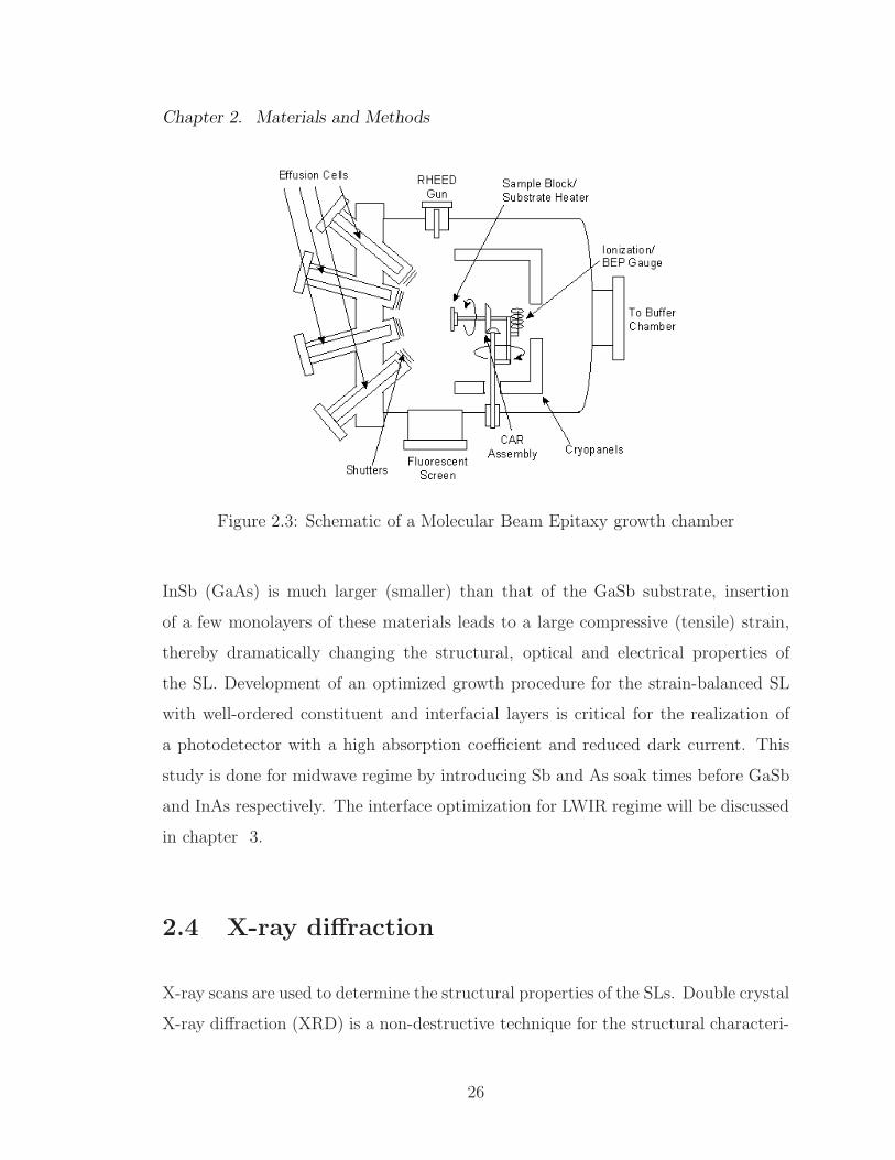
2.3 Schematic of a Molecular Beam Epitaxy growth chamber . . . . . . 26
xv

List of Figures
2.4 Schematic diffraction of X-rays in the crystal . . . . . . . . . . . . . 27
2.5 Typical XRD spectrum from InAs/GaSb SL . . . . . . . . . . . . . 28
2.6 Essential components of atomic force microscopy (AFM) . . . . . . . 31
2.7 (a) Optical absorption measurement set-up, sample holder is loaded
in the main compartment of the FTIR (b) Brewster angle sample
holder (c) Normal incidence sample holder . . . . . . . . . . . . . . 32
2.8 Schematics of the masks used in fabrication process of the superlat-
tice detectors . . . . . . . . . . . . . . . . . . . . . . . . . . . . . . 34
2.9 Conventionally processed pin diode . . . . . . . . . . . . . . . . . . 34
2.10 Spectral response measurement setup . . . . . . . . . . . . . . . . . 36
2.11 Responsivity measurement setup . . . . . . . . . . . . . . . . . . . . 37
3.1 (a) electron and hole wavefunctions (b) dispersion diagram at 0 K
for 2.4 nm GaSb/2.4 nm InAs. . . . . . . . . . . . . . . . . . . . . . 41
3.2 Estimation of the growth rates by X-ray scan of SLs width different
period . . . . . . . . . . . . . . . . . . . . . . . . . . . . . . . . . . . 42
3.3 shutter sequence for the growth of MW SLs . . . . . . . . . . . . . . 43
3.4 A schematic of pin InAs/GaSb SL MWIR detector . . . . . . . . . . 44
3.5 A schematic of processed MW SL pin detector . . . . . . . . . . . . 45
3.6 (a) Dark current density, and (b) spectral response of MWIR pin SL
detector . . . . . . . . . . . . . . . . . . . . . . . . . . . . . . . . . . 46
3.7 (a) band alignment, and electron/hole wavefunctions (b) dispersion
diagram of 13 MLs of InAs and 7 MLs of GaSb . . . . . . . . . . . . 47
xvi

List of Figures
3.8 (a) band alignment, and electron/hole wavefunctions (b) dispersion
diagram of 13 MLs of InAs, 0.45 ML of strain compensating layer of
InSb and 7 MLs of GaSb . . . . . . . . . . . . . . . . . . . . . . . . 48
3.9 Electron and hole wavefunction overlap and cutoff wavelength for 8
MLs GaSb/ X MLs InAs ( X= 8, 10, 12, 14). . . . . . . . . . . . . 49
3.10 The temperature of (1×3) to (2×5) reconstruction transition was
taken as a reference for the growth temperatures. . . . . . . . . . . . 51
3.11 Growth optimization for LWIR structure using (a) InSb layer (b)
group V soak time. . . . . . . . . . . . . . . . . . . . . . . . . . . . 53
3.12 Growth temperature optimization for LWIR structure . . . . . . . . 55
3.13 LWIR nBn structure (b) XRD of LWIR nBn structure, almost zero
% lattice mismatch between SL and GaSb substrate and 19 arcsec
FWHM for the first satellite peak. . . . . . . . . . . . . . . . . . . . 56
3.14 Cross-sectional STEM images of an nBn detector . . . . . . . . . . . 57
3.15 (a) Schematic of LWIR SL pin detectors; represents three samples
with different absorber region doping levels (b) HRXRD of the non-
intentionally doped LWIR SL pin detector. . . . . . . . . . . . . . . 60
3.16 Dark current density at 77 K for the three pin structures. . . . . . . 61
3.17 (a) Responsivity and (b) detectivity measurements of the pin devices
at 77 K . . . . . . . . . . . . . . . . . . . . . . . . . . . . . . . . . . 64
3.18 Schematic of nBn design. Majority carriers (electrons) are blocked
by the barrier and minority carriers (holes) are the source of current. 65
3.19 (a) Structure schematic (b) HRXRD of the LWIR nBn detector. . . 68
xvii

List of Figures
3.20 Main processing steps for LWIR nBn detectors . . . . . . . . . . . . 69
3.21 (a) Shallow etch processing (b) deep etch processing (c) shallow etch
processing with indication of diffusion lengths. . . . . . . . . . . . . 70
3.22 Dark current density of shallow, and deep etched nBn devices vs tem-
perature. This comparison shows the effect of dark current density
reduction due to reduction of surface leakage currents. . . . . . . . . 71
3.23 (a) Responsivity and (b) detectivity measurements of the nBn device
at 77 K . . . . . . . . . . . . . . . . . . . . . . . . . . . . . . . . . . 72
3.24 Spectral response of (a) pin (b) nBn structure, 8 µm cutoff wave-
length is shown in the two diagrams. . . . . . . . . . . . . . . . . . . 73
3.25 Dark current density at 77 K for nBn and pin structures . . . . . . . 74
3.26 (a) Responsivity and (b) detectivity measurements of the pin and
nBn devices at 77 K; nBn structure has the highest responsivity and
detectivity values as compared to the pin structure. . . . . . . . . . 75
4.1 (a) mid-wave infrared image (b) long-wave infrared image (c)long-
wave subtracted from midwave images taken to locate fire spots from
South America lands. . . . . . . . . . . . . . . . . . . . . . . . . . . 80
4.2 (a) cross-section schematic, and (c) typical I-V characteristic for a
single-mesa, single-indium bump, dual-color detector design. With
the appropriate polarity and voltage bias at the pixel contact, the
Band 1 and Band 2 p-n junctions respond to shorter and longer
wavelength infrared radiation, respectively. . . . . . . . . . . . . . . 82
4.3 (a) Schematic (b) SEM picture of two-color InAs/GaSb superlattice
detector . . . . . . . . . . . . . . . . . . . . . . . . . . . . . . . . . . 83
xviii

List of Figures
4.4 (a) structure A: two color MWIR detector (λc1 ∼ 3.5 µm and λc2 ∼4.5 µm) and b) structure B: dual band MW-LWIR (λc1 ∼ 3.5 µm
and λc2 ∼ 8.0 µm). . . . . . . . . . . . . . . . . . . . . . . . . . . . 84
4.5 Current density at different temperatures for both shallow and deep
etched devices. . . . . . . . . . . . . . . . . . . . . . . . . . . . . . . 85
4.6 Current density at different temperatures for (a) structure A and (b)
structure B. . . . . . . . . . . . . . . . . . . . . . . . . . . . . . . . 87
4.7 Spectral response of structure (a) A and (b) B at different tempera-
tures under forward bias and reverse ;Vbis the applied voltage to the
device. . . . . . . . . . . . . . . . . . . . . . . . . . . . . . . . . . . 88
4.8 Two color nBn detector under (a) forward bias and (B) reverse bias 89
4.9 The responsivity (solid black line, left axis) and quantum efficiency
(dotted red line, right axis) for (a) structure A, and (b) structure B. 90
4.10 Structure C: Dual band MWIR/LWIR detector . . . . . . . . . . . . 91
4.11 Dark current density of two-color SL detector (structure C) . . . . . 92
4.12 Spectral response of the bi-color structure at different temperatures
under forward and reverse bias ;Vb is the applied voltage. . . . . . . 92
4.13 (a)The spectral response of structure C between 0 and +0.1V bias
voltage, that is compatible with the bias range of present day ROICs.
(b) the intensity study of MWIR, LWIR, and MWIR to LWIR ratio
vs applied bias voltage at 77 K. . . . . . . . . . . . . . . . . . . . . 94
xix

List of Figures
5.1 Cross-sectional TEM image of 120 nm of GaSb on GaAs showing a
highly periodic array of misfit dislocations at the GaSb layer and the
GaAs substrate [1]. . . . . . . . . . . . . . . . . . . . . . . . . . . . 98
5.2 a) Hall resistivity, b) Hall carrier concentration, and c) Hall mobility
of non-intentionally doped mid-wave SL versus measurement tem-
perature; SL is residually p-type at temperatures below 200 K and
n-type at temperatures above 200 K. From Hall resistivity two ac-
tivation energies of 193 meV and 23.86 meV were extracted which
indicates existence of shallow and deep impurity levels in the SL. . . 101
5.3 a) Hall resistivity of non-intentionally doped long-wave SL versus
measurement temperature, b) Hall carrier concentration versus mea-
surement temperature, and c) Hall carrier concentration dependence
on growth temperature; SL is residually n-type at all of the mea-
surement temperatures. At low measurement temperatures extrinsic
carriers and at high measurement temperatures intrinsic carriers are
the dominant source of carriers in the LW SL. . . . . . . . . . . . . 103
5.4 a) Hall mobility versus measurement temperature, and b) Hall peak
mobility of non-intentionally doped long-wave SL versus growth tem-
perature; As the growth temperature increases, interface scattering
becomes the dominant source of scattering in the SL which decreased
the mobility and causes temperature independent behavior of the
mobility. Also due to interface roughness scattering peak mobility
decreases. . . . . . . . . . . . . . . . . . . . . . . . . . . . . . . . . . 104
5.5 (a) Long-wave SL structure schematic (b) HRXRD of the sample
grown at Tt-45◦C used for transport studies. . . . . . . . . . . . . . 106
5.6 Main steps of processing for substrate removal (flip-chip method) . . 107
xx

List of Figures
5.7 Classical form of the sample for van der Pauw method measurements. 108
5.8 The van der Pauw configuration for lateral LW SL transport studies 108
5.9 (a) Hall experimental data for magnetic field rang of 0-12 T (b) Mo-
bility spectra obtained from QMSA algorithm at 77 K (c) Mobility
spectra obtained from QMSA algorithm at temperature range of 32-
290 K. . . . . . . . . . . . . . . . . . . . . . . . . . . . . . . . . . . 112
5.10 (a) Carrier concentration versus 1/T for LWIR SLs on GaSb sub-
strate; Two activation energies are extracted, indicating (b) shallow
impurity donor levels close to the SL conduction band . . . . . . . . 113
6.1 Mechanical and chemical processing steps for GaSb substrate removal 120
6.2 SL sample geometry for vertical transport study . . . . . . . . . . . 120
6.3 (a) next-nano band alignment simulation of 16 MLs InAs/0.86 MLs
InSb/7 MLs GaSb (b) next-nano dispersion diagram which indicates
a cut-off wavelength of 12 µm at 0 K (c) Growth optimization for
VLWIR SL structure using InSb strain compensating layer . . . . . 124
xxi

List of Tables
1.1 Subdivisions of the infrared spectrum . . . . . . . . . . . . . . . . . 3
1.2 Some important parameters for InAs and GaSb at 300 K . . . . . . 17
1.3 A summary of reported MW/LW/VLW IR . . . . . . . . . . . . . . 19
3.1 Summary of dark current density, responsivity and detectivity of pin
and nBn devices measured at 77 K, 7 µm. . . . . . . . . . . . . . . . 76
xxii
Chapter 1
Introduction
In this chapter general concept of infrared detection, infrared detectors and their
figures of merit are introduced. Different types of infrared detectors and competing
technologies and their advantages/disadvantages are covered. Finally, an alternative
detector technology, type II InAs/(In)GaSb superlattice based detectors, for Mid-
wave and Long-wave infrared detection is introduced.
1.1 Basics of infrared detection
An electromagnetic spectrum is the distribution of all electromagnetic waves ar-
ranged according to their wavelength or corresponding energy (see figure 1.1).
The infrared region of the electromagnetic spectrum corresponds to the region
that is bounded on the short-wavelength side by visible light and on the long-
wavelength side by microwaves. Since heated objects radiate energy in infrared, this
region of the electromagnetic spectrum is referred to as the heat region as well. The
infrared region of the electromagnetic spectrum is divided into subdivisions based
on the atmospheric absorption. IR spectral region are affected by strong absorptions
1

Chapter 1. Introduction
Figure 1.1: The Electromagnetic Spectrum
due to molecules in the earth’s atmosphere, particularly CO2 and H2O and Ozon.
Some minor constituents, including carbon monoxide, nitrous oxide, methane, and
nitric oxide, are less significant absorbers. The transmission of IR in atmosphere is
shown in figure 1.2.
Figure 1.2: Transmission of IR in atmosphere
The atmosphere is relatively transparent from about 3 to 5 µm and 8 to 13
µm. These regions are referred to as atmospheric windows and are commonly used
2

Chapter 1. Introduction
by IR detectors. The infrared spectrum considering the atmospheric absorption is
subdivided in to five regions which are summarized in the table below:
Table 1.1: Subdivisions of the infrared spectrum
Designation Abbreviation Limits(µm)
Near Infrared Radiation NIR 0.7-1.5Short Wavelength Infrared Radiation SWIR 1.5-2.5Medium Wavelength Infrared Radiation MWIR 3-5Long Wavelength Infrared Radiation LWIR 8-12Very Long Wavelength Infrared Radiation VLWIR 12-32
1.1.1 Thermal Radiation Laws
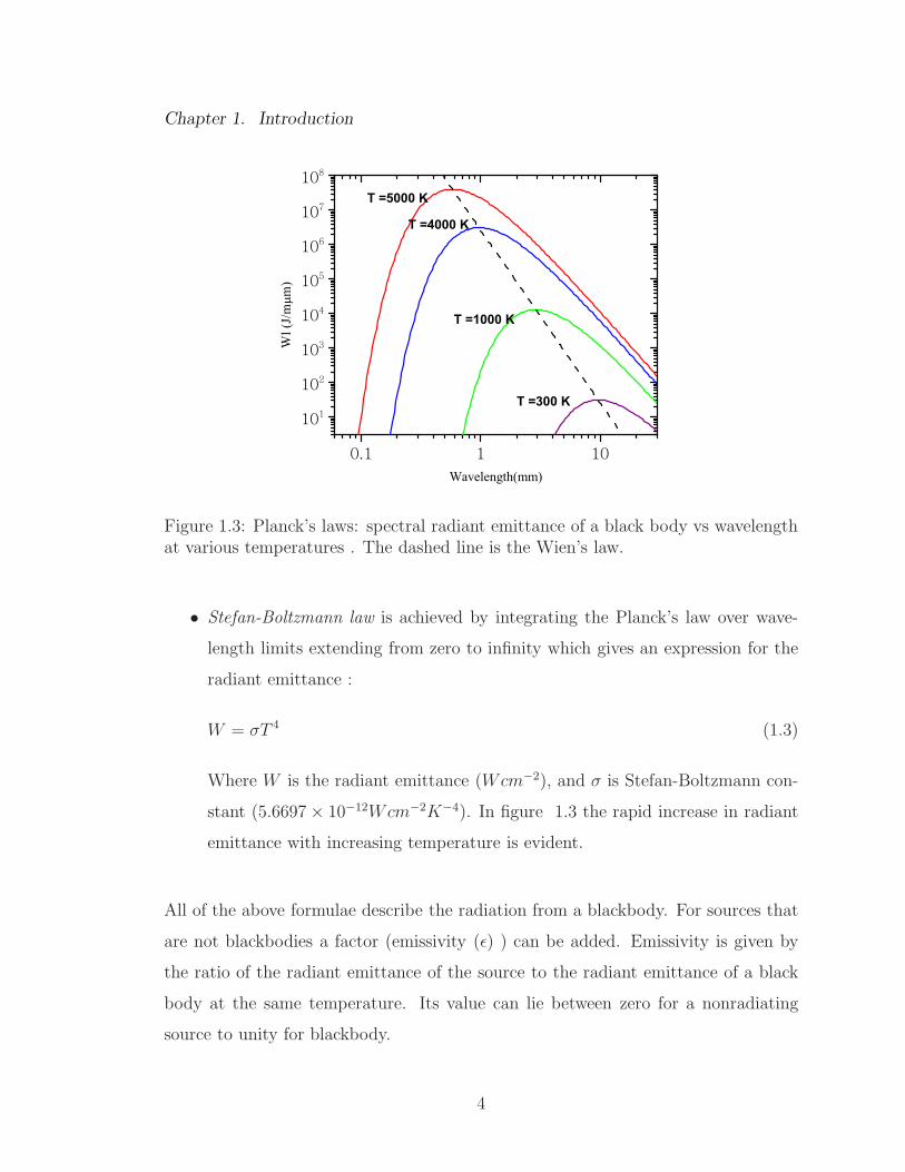
• Planck’s law describes the spectral distribution of the radiation from a black-
body as ( see figure 1.3)
Wλ =2πhc2
λ5
1
e
hc
λkT − 1
(1.1)
Where Wλ is spectral radiant emittance (Wcm−2µ−1), k is the Boltzmann’s
constant, h is the plank’s constant and c is the speed of th light. This law
describes the probability distribution of emitted wavelengths at a given tem-
perature.
• Wien’s displacement law describes the wavelength at which the maximum spec-
tral radiant emittance occurs,
λm(µm) =2898
T (K). (1.2)
It is derived differentiating Plank’s law and then solving for the maximum
spectral radiant emittance. The wavelength varies inversely with the absolute
temperature as expressed by equation 1.2.
3
Chapter 1. Introduction
0.1 1 10
101
102
103
104
105
106
107
108
T =300 K
T =1000 K
T =4000 K
Wl (
J/m
m)
Wavelength(mm)
T =5000 K
Figure 1.3: Planck’s laws: spectral radiant emittance of a black body vs wavelengthat various temperatures . The dashed line is the Wien’s law.
• Stefan-Boltzmann law is achieved by integrating the Planck’s law over wave-
length limits extending from zero to infinity which gives an expression for the
radiant emittance :
W = σT 4 (1.3)
Where W is the radiant emittance (Wcm−2), and σ is Stefan-Boltzmann con-
stant (5.6697× 10⁻¹²Wcm−2K−4). In figure 1.3 the rapid increase in radiant
emittance with increasing temperature is evident.
All of the above formulae describe the radiation from a blackbody. For sources that
are not blackbodies a factor (emissivity (ǫ) ) can be added. Emissivity is given by
the ratio of the radiant emittance of the source to the radiant emittance of a black
body at the same temperature. Its value can lie between zero for a nonradiating
source to unity for blackbody.
4

Chapter 1. Introduction
1.2 Infrared detectors
The central element of any IR detection system is the detector. The detector is the
device which converts an optical signal into some other form, in most cases, electrical.
By the method of transduction, detectors may be divided in two classes: thermal
detectors and photon detectors.
1.2.1 Thermal Detectors
When thermal detectors are heated by incoming IR radiation their temperature in-
creases and the temperature changes are measured by any temperature-dependent
mechanism, such as voltage, or resistance. The main advantage of the thermal detec-
tors is their room temperature operation without any requirement for cooling which
has made them a good candidate in spaceborne applications. The main disadvantage
of thermal detectors is their long time constant which is usually a few milliseconds
or longer and therefore, they are rarely used in applications that high data rates are
required. The most common thermal detectors providing an electrical output are:
• Bolometers are the thermal detectors which their electrical resistance changes
when heated by the incident radiation.
• Thermocouples consist of two dissimilar metals, joined together at one end.
When infrared radiation is absorbed by the junction of the two metals, a volt-
age is produced that can be correlated back to the temperature. Several ther-
mocouples connected in series form a thermopile.
• Pyroelectric detectors operate when a change occurs in the temperature due
to a change in incident radiation which causes an electrical polarization of the
material. This polarization change occurs on the surface of the element creating
a current that can be measured.
5
Chapter 1. Introduction
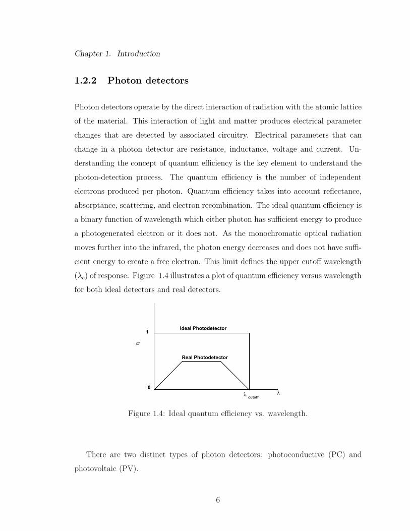
1.2.2 Photon detectors
Photon detectors operate by the direct interaction of radiation with the atomic lattice
of the material. This interaction of light and matter produces electrical parameter
changes that are detected by associated circuitry. Electrical parameters that can
change in a photon detector are resistance, inductance, voltage and current. Un-
derstanding the concept of quantum efficiency is the key element to understand the
photon-detection process. The quantum efficiency is the number of independent
electrons produced per photon. Quantum efficiency takes into account reflectance,
absorptance, scattering, and electron recombination. The ideal quantum efficiency is
a binary function of wavelength which either photon has sufficient energy to produce
a photogenerated electron or it does not. As the monochromatic optical radiation
moves further into the infrared, the photon energy decreases and does not have suffi-
cient energy to create a free electron. This limit defines the upper cutoff wavelength
(λc) of response. Figure 1.4 illustrates a plot of quantum efficiency versus wavelength
for both ideal detectors and real detectors.
Real Photodetector
0
1
cutoff
Ideal Photodetector
Figure 1.4: Ideal quantum efficiency vs. wavelength.
There are two distinct types of photon detectors: photoconductive (PC) and
photovoltaic (PV).
6
Chapter 1. Introduction
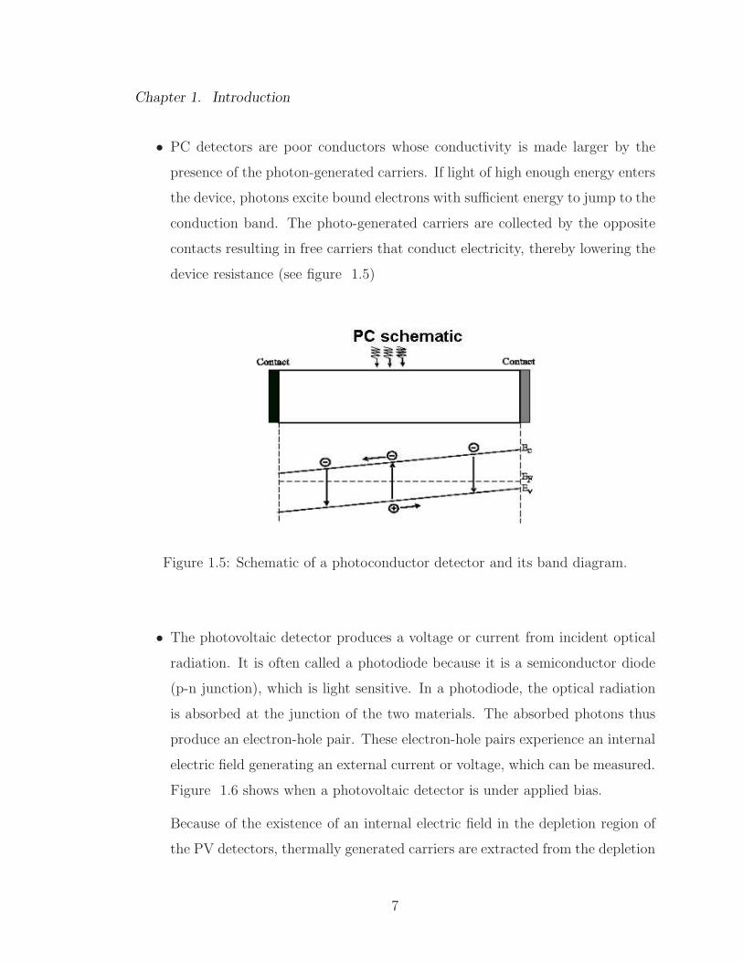
• PC detectors are poor conductors whose conductivity is made larger by the
presence of the photon-generated carriers. If light of high enough energy enters
the device, photons excite bound electrons with sufficient energy to jump to the
conduction band. The photo-generated carriers are collected by the opposite
contacts resulting in free carriers that conduct electricity, thereby lowering the
device resistance (see figure 1.5)
Figure 1.5: Schematic of a photoconductor detector and its band diagram.
• The photovoltaic detector produces a voltage or current from incident optical
radiation. It is often called a photodiode because it is a semiconductor diode
(p-n junction), which is light sensitive. In a photodiode, the optical radiation
is absorbed at the junction of the two materials. The absorbed photons thus
produce an electron-hole pair. These electron-hole pairs experience an internal
electric field generating an external current or voltage, which can be measured.
Figure 1.6 shows when a photovoltaic detector is under applied bias.
Because of the existence of an internal electric field in the depletion region of
the PV detectors, thermally generated carriers are extracted from the depletion
7

Chapter 1. Introduction
Figure 1.6: Schematic of a pin detector and its corresponding band diagram.
region which would not have the chance of recombination in the depletion
region. However, since the internal electric field does not exist in the PC
detectors, recombination is an added factor to the dark current. Thus dark
current in PV is smaller as compared to PC detectors.
1.3 Figures of merit for infrared detectors
Figures of merit enable user to compare relative performance among different de-
tectors. These figures of merit are applicable to any type of detector, and are in-
dependent of the generic optical-detector process. Most of the figures of merit are
expressed in energy based units due to historical reasons. The general figures of
merit are: responsivity, noise equivalent power, and detectivity.
8

Chapter 1. Introduction
1.3.1 Responsivity
The spectral responsivity is defined as the output per watt of monochromatic ra-
diation. The output can be either current or voltage, per watt of monochromatic
radiation. Photogenerated carries are expressed as:
ig = ηΦqq (1.4)
Where ig is the photogenerated carriers, η is the quantum efficiency, and Φq is the
phonon flux measured in photons/sec.
Using the above definition for the photogenerated carriers, responsivity is defined
as following:
Ri =igΦe
=ηΦqq
Φe
(1.5)
Where Φe is the radiant power (flux) input given in watts.
The radiant power is related to the photon flux by:
Φe =hc
λΦq (1.6)
Therefore, responsivity is:
R(λ) =ηΦqqλ
Φqhc=
λ
hcqη (1.7)
Equation 1.7 gives the relation between quantum efficiency and current responsivity
as a function of wavelength for photon detectors.
Although responsivity of a detector is useful to predict an expected signal level
for a given radiant power on the detector, the responsivity is of limited usefulness
from a sensitivity point of view. In addition to the signal level, the noise level must
also be considered to quantify the signal-to-noise ratio (SNR).
9
Chapter 1. Introduction
1.3.2 Noise Equivalent Power
The minimum radiant-flux level a detector can discern depends on the detector noise
level. The signal current produced by the input power must be above the noise
current to be easily detected. The SNR can be expressed as responsivity:
S
N=
RΦe
in(1.8)
Where R is the responsivity, Φe is the radiant power (flux) in watts, and in is the
noise current.
The radiant power, Φe incident on a detector that yields SNR=1 is called the
noise-equivalent-power. Setting equation 1.8 equal to 1 and solving for the required
power,
Φe =inR
=Φe
isig/in(1.9)
Where isig/in is the current SNR. As the responsivity is a function of wavelength
and frequency, so is NEP. The units of which are watts. The NEP can also be found
using the voltage noise and the voltage responsivity. A more sensitive detector will
have a lower NEP. To compare NEP of different detectors, parameters like optically
active detector area, noise-equivalent electrical bandwidth, and other measurement
parameters needs to be taken into account. An important parameter that facili-
tates comparison among different detectors with different geometries is the specific
detectivity (D∗).
1.3.3 Detectivity
The figure of merit D∗ called normalized detectivity is:
D∗ =
√Ad∆f
NEP(1.10)
10

Chapter 1. Introduction
where Ad is the area of the detector and ∆f is the bandwidth of the measure-
ment. This figure of merit is sensitivity normalized to a 1-cm2 area and 1-Hz
noise-equivalent bandwidth. It can be interpreted as an SNR out of a detector
when 1 W of radiant power is incident on the detector, given an area equal to 1
cm2 and noise-equivalent bandwidth of 1 Hz. The units of D∗ are Jones defined as
[cm√Hz/watt]=[Jones]. D∗ can be related to the responsivity by:
D∗ =R√Ad
in/√∆f
(1.11)
D∗ allows for comparison between detectors regardless of size or measurement pa-
rameters.
1.4 Focal Plane Arrays (FPAs)
A Focal Plane Array (FPA) is the main component used in advanced infrared imag-
ing systems. An IR FPA is an array of single pixel devices used to capture an
infrared signal. FPAs increase the efficiency of collection compared to a single pixel
by decreasing acquisition time. Both thermal and photon detectors can be made into
FPAs.
1.4.1 Thermal detector FPAs
Thermal focal plane arrays are typically operated at ambient temperature. Because
thermal detection involves heating phenomena, and the temperature change process
is slow, thermal FPAs have slow response. They also have low sensitivity. The
fundamental limit to the sensitivity of any thermal detector is set by temperature
fluctuation noise, i.e., random fluctuations in the temperature of the detector element
due to fluctuations in the radiant power exchange between the detector and its
11

Chapter 1. Introduction
surroundings. On the other hand, in thermal FPAs the response is independent
of wavelength, which is important for LWIR applications. They are also cheap and
convenient to use. They have found widespread use in low cost applications, which
do not require high performance and speed. They are frequently used in infrared
spectrometers.
1.4.2 Photon detector FPAs
The first two generations of IR detectors were used in scanning and staring systems
for military and civilian applications. The simplest scanning system consists of a
row of detectors; The two-dimensional (2-D) image is generated by scanning the
scene across the strip using a mechanical scanner. First generation scanning systems
used linear arrays of intrinsic HgCdTe sensors. The invention of charge coupled
devices (CCD) coupled with advances in silicon chip technology helped development
of second generation detector arrays containing larger number of detector elements
(staring systems). A staring system is a two-dimensional (2-D) array of detector
pixels which are scanned electronically by circuits integrated with the arrays [2]. 2-
D arrays used in staring systems have higher sensitivity as compared to the scanning
systems due to their larger number of pixels. Higher frame rates are also achievable
by electronic scanners in staring systems as compared to the mechanical scanners
in scanning systems. Medium format 320×240 2D arrays operating in MWIR range
were made with HgCdTe or indium antimonide detectors. Although the first and
second generation IR detectors provided promising results in the MWIR and LWIR
range, the need for larger number of pixels (2K×2K pixels), higher frame rates, better
thermal resolution and multi-color functionally led to third generation IR detectors
[2].
12
Chapter 1. Introduction
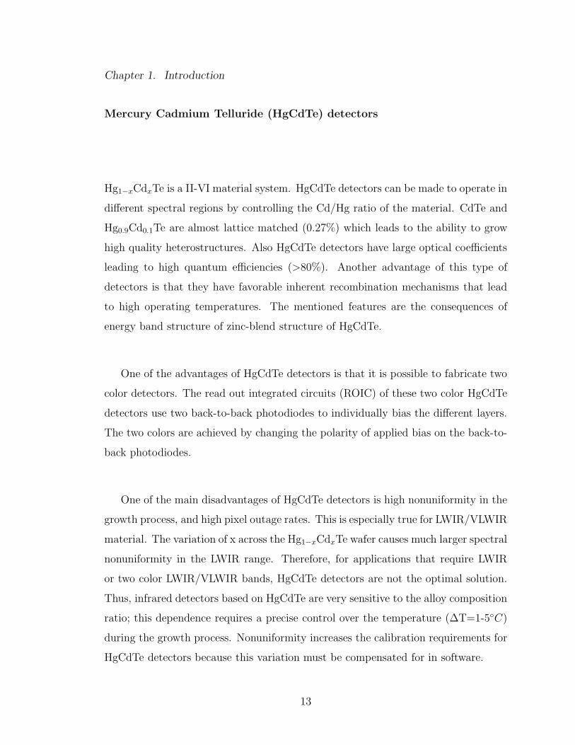
Mercury Cadmium Telluride (HgCdTe) detectors
Hg1−xCdxTe is a II-VI material system. HgCdTe detectors can be made to operate in
different spectral regions by controlling the Cd/Hg ratio of the material. CdTe and
Hg0.9Cd0.1Te are almost lattice matched (0.27%) which leads to the ability to grow
high quality heterostructures. Also HgCdTe detectors have large optical coefficients
leading to high quantum efficiencies (>80%). Another advantage of this type of
detectors is that they have favorable inherent recombination mechanisms that lead
to high operating temperatures. The mentioned features are the consequences of
energy band structure of zinc-blend structure of HgCdTe.
One of the advantages of HgCdTe detectors is that it is possible to fabricate two
color detectors. The read out integrated circuits (ROIC) of these two color HgCdTe
detectors use two back-to-back photodiodes to individually bias the different layers.
The two colors are achieved by changing the polarity of applied bias on the back-to-
back photodiodes.
One of the main disadvantages of HgCdTe detectors is high nonuniformity in the
growth process, and high pixel outage rates. This is especially true for LWIR/VLWIR
material. The variation of x across the Hg1−xCdxTe wafer causes much larger spectral
nonuniformity in the LWIR range. Therefore, for applications that require LWIR
or two color LWIR/VLWIR bands, HgCdTe detectors are not the optimal solution.
Thus, infrared detectors based on HgCdTe are very sensitive to the alloy composition
ratio; this dependence requires a precise control over the temperature (∆T=1-5◦C)
during the growth process. Nonuniformity increases the calibration requirements for
HgCdTe detectors because this variation must be compensated for in software.
13

Chapter 1. Introduction
Quantum well infrared photodetectors (QWIPs)
Another alternative infrared technology for MWIR and LWIR bands is the quantum
well infrared photodetectors (QWIPs). QWIPs are commercially fabricated using the
GaAs/AlGaAs quantum well material system. In QWIP detectors, the low bandgap
material acts as a trap for the electron. The electrons stay in the well until excited by
incoming photons, until they gain enough energy to escape the well. When electrons
obtain enough energy to leave the well, they contribute to the device current. The
number and levels of discrete energy states in a well can be changed by the variations
in the depth and width of the well. Absorption of LW radiation in a wide quantum
well can originate from bound to bound state transitions [3]. Thus, when a photon
hits the quantum well with energy equal or greater than the energy difference between
the two states, an electron in the ground state is excited to the first excited state. Via
an applied voltage, these excited electrons can be extracted (and thus can contribute
to the photocurrent). The energy levels and thus the absorption wavelength can be
adjusted by changing thickness of constituent well (GaAs) and barrier (AlxGa1−xAs)
layers. The schematic diagram of GaAs/AlGaAs QWIP is shown in figure 1.7.
Figure 1.7: Schematic diagram of GaAs/AlGaAs QWIP
GaAs/AlGaAs QWIPs have the following advantages:
• Use of standard manufacturing techniques based on mature GaAs growth and
14

Chapter 1. Introduction
processing techniques
• Highly uniform and well-controlled MBE growth on large substrates(6”)
• GaAs wafers are low cost, and have high thermal stability
However, QWIP detectors have high values of thermally generated dark current
which is caused by electron tunneling between wells,resulting in a low signal-to-noise
ratio. Due to intersubband transitions in QWIPs, LWIR QWIPs have performance
limitation especially at higher temperatures (>70 K). Also, due to absorption selec-
tion rules, optical transition is forbidden for normal incidence of light; this limitation
is usually overcome by the incorporation of a grating on the detector surface, however
this drastically limits the quantum efficiency (typically less than 10%) [4].
InSb detetectors
Indium antimonide (InSb) is one of the most highly developed and widely used de-
tector materials for the near-infrared portion of the spectrum (1 to 5 µm). InSb is a
member of the III-V semiconductor materials. The crystal structure of pure InSb is
cubic zinc-blend. The p-type material is formed if more indium is used in the com-
pound and an n-type material is formed if more antimony is used. Indium material is
an intrinsic semiconductor with a direct room energy band-gap of 0.17 eV . Thermally
generated carriers are the dominant noise source at high temperature requiring InSb
detectors to be cryogenically cooled. Large uniform substrates are available allowing
for fabrication of large area FPAs (1024×1024 pixels). InSb detectors are used in
forward looking infrared heat seeking missiles and thermal imaging. The drawbacks
of the material system include the cooling requirement, the material specific cutoff
wavelength limit and the tendency of the FPA characteristics to drift between uses.
15
Chapter 1. Introduction
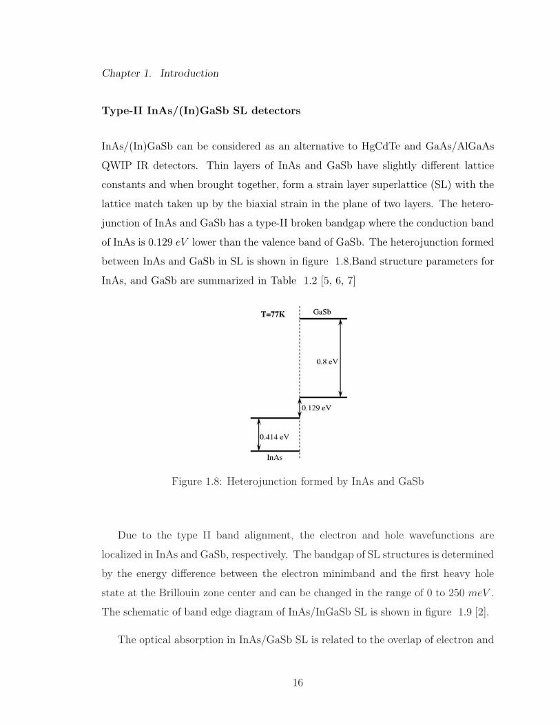
Type-II InAs/(In)GaSb SL detectors
InAs/(In)GaSb can be considered as an alternative to HgCdTe and GaAs/AlGaAs
QWIP IR detectors. Thin layers of InAs and GaSb have slightly different lattice
constants and when brought together, form a strain layer superlattice (SL) with the
lattice match taken up by the biaxial strain in the plane of two layers. The hetero-
junction of InAs and GaSb has a type-II broken bandgap where the conduction band
of InAs is 0.129 eV lower than the valence band of GaSb. The heterojunction formed
between InAs and GaSb in SL is shown in figure 1.8.Band structure parameters for
InAs, and GaSb are summarized in Table 1.2 [5, 6, 7]
Figure 1.8: Heterojunction formed by InAs and GaSb
Due to the type II band alignment, the electron and hole wavefunctions are
localized in InAs and GaSb, respectively. The bandgap of SL structures is determined
by the energy difference between the electron minimband and the first heavy hole
state at the Brillouin zone center and can be changed in the range of 0 to 250 meV .
The schematic of band edge diagram of InAs/InGaSb SL is shown in figure 1.9 [2].
The optical absorption in InAs/GaSb SL is related to the overlap of electron and
16

Chapter 1. Introduction
Table 1.2: Some important parameters for InAs and GaSb at 300 K
Parameters InAs GaSb
Lattice constant (A) 6.0583 6.0959Energy gap (eV ) 0.356 0.725
Valence band offset (eV ) 0.56 (300 K) 0.482 (77K) 0Electron mobility (cm2/V.s) 20000 5000Hole mobility (cm2/V.s) 480 880
Dielectric constant 15.15 15.69me/m0 0.0183 0.042mhh/m0 0.263 0.222mlh/me 0.0247 0.045mso/me 0.0557 0.075
Figure 1.9: Band edge diagram illustrating the confined electron and hole minibandswhich form the energy band gap.
hole wavefunctions. Thin layers of SL have large overlap wavefunctions and therefore
large absorption coefficients. The overlap between the wavefunction appear near the
hetero-interfaces and therefore the optical absorption is restricted to the vicinity
of interfaces [8]. From the mentioned characteristics of InAs/GaSb SL, one can
conclude that by atomic engineering of the superlattice interfaces and by changing
the thicknesses of InAs and GaSb, we can change the detector cutoff wavelength from
3 to more than 40 µm. The main advantages of SL are as following:
17

Chapter 1. Introduction
• Normal incidence absorption due to interminiband transitions
• Tunable cutoff wavelengths due to adjustable bandgap
• Supression of Auger related dark current based on SL band structure engineer-
ing [9] (quantum confinement and large splitting of heavy-hole and light-hole
valence subbands in SL)
• Reduction of tunneling currents due to large electron effective mass
• High uniformity due to mature III-V semiconductor materials growth tech-
niques
All of the above features lead to higher operation mode for SL photodetectors as
compared to the state of the art HgCdTe detectors, InSb detectors, and QWIPs.
InAs/(In)GaSb SL detectors have been reported by different groups in MWIR,
LWIR, and VLWIR regions. Table 1.3 provides an overview of different SL single
pixel detector performance results.
1.5 Conclusion
General concepts concerning infrared detection were presented followed by descrip-
tion of different technologies for infrared imaging. Thermal detectors have the ad-
vantage of room-temperature operation however, they have low sensitivity and are
very slow as compared to the photon detectors. IR detector figures of merit were
discussed in detail. Competitive third generation FPAs material systems were cov-
ered with their disparate strengths and weaknesses, providing motivation for other
material systems to overcome the present photon detector limitations. Detectors
based on InAs/GaSb SL were presented as an alternative technology which has all
18

Chapter 1. Introduction
Table 1.3: A summary of reported MW/LW/VLW IR
Superlattice Device D∗
λc η Ref.type type [Jones]12ML InAs/7ML GaSb P-on-n 10 µm 46% [10]
Barrier14ML InAs/7ML GaSb 9.9 µm 29% 1011 [11]type
Barrier16ML InAs/9ML GaSb 14 µm 17.5% 1010 [12]type
5 µm8ML InAs /11ML GaSb n-on-p @ 25% 109 [13]
300 K7 µm 12-
9ML InAs /4ML GaSb n-on-p @ 1012 [14]77 K 32%
14ML InAs/7ML GaSb n-on-p 11 µm 36% [15]W-Structure 10.5µm 20-
14ML InAs/9ML GaSb p-on-n @ [16]14ML InAs/7ML Al0.4Ga0.49/In0.11Sb 78 K 34%
M-Structure 10.5µm18ML InAs/3ML GaSb n-on-p @ 27% [16]/5ML AlSb/3ML GaSb 77 K
4.5µmDual band nBn and [17]
∼8µm11µm
Dual band n-on-p and 4-5% [18]∼17µm
of the advantages of the state of the art photon detectors as well as potential to
overcome the existing limitations in the competing technologies. It has principal
advantages like flexibility of the material system allowing multispectral detection,
lower tunneling currents due to higher electron effective masses and mature III-V
epitaxial growth technology.
The recently proposed nBn heterostructure design has demonstrated a 100 K in-
crease in background-limited infrared photodetection (BLIP) for InAs-based device,
by decreasing Shockley-Read-Hall generation currents and by suppressing surface
currents using specific processing.
19
Chapter 1. Introduction
Third generation IR detectors have three main emphasis, High operating temper-
ature (HOT), multicolor capability, and large format arrays. This work concentrates
on multicolor and HOT IR detectors based on nBn design. Contributions of this the-
sis include, 1) Development of design and growth procedure for the LW SL detectors
leading to an improved detector performance. 2) Optical and electrical characteris-
tics of single pixel devices in the MWIR, LWIR, and bi-color SL detectors. 3) Careful
evaluation of carrier transport in SL in order to understand and improve SL device
performance.
20

Chapter 2
Materials and Methods
2.1 Introduction
This chapter covers the design and experimental methods required for testing of
infrared photodetectors. First, design tools for analyzing different SL systems and
structures are introduced. Next section covers Molecular Beam Epitaxy (MBE)
technique. MBE growth of SL material is the first step in the realization of IR pho-
todetectors. X-ray diffraction (XRD) measurements are used to study the structural
properties of as-grown material, and atomic force microscopy (AFM) is used to image
and evaluate the surface morphology of the materials.
The bandgap of the as-grown materials is determined by optical absorption mea-
surements. After growth and non-destructive structural and optical measurements,
single pixel devices are processed using standard photolithography methods. The
electrical behavior of the processed detectors was investigated by current-voltage (I-
V) measurements. Detector performance also was characterized by spectral response
and responsivity measurements.
21

Chapter 2. Materials and Methods
2.2 Design tools
To lower the cost, and time associated with experimental processes used for testing
SLs (growth, processing, characterization) first principle calculations were performed
using commercially available softwares. These simulation are used to predict the
band gap of the SL material and to optimize the designs to achieve the best device
performance.
The main design parameters involving the SL material system are: the cutoff
wavelength associated with different thicknesses of different SL constituent materi-
als, and absorption of the SL which is directly related to the electron and hole wave-
functions overlap. To design the SL material system targeted at a specific region
of the infrared spectrum as well as to study the absorption of that material system
next-nano software is used. Next-nano software implements the 8×8 k.p modeling
which is an approximation scheme for calculating the band structure (particularly
effective mass) and optical properties of crystalline solids [19, 20, 21].
To study the device characteristics such as energy band alignment of the struc-
tures as well as dark current at different applied biases Sentaures TCAD software is
used. Sentaurus combines advanced, calibrated physical models, robust algorithms
and numeric, and efficient meshing and structure editing capabilities to generate
accurate and predictive simulation results.
a. Nextnano software [22] is used generally for the simulation of electronic and
optoelectronic semiconductor nanodevices and materials. For the design of the
SLs 8×8 k.p method is used to generate the electron and hole wavefunctions
in the SL layers. The 8×8 k.p provides the dispersion diagram of the simu-
lated structure which the cutoff wavelength at different temperatures can be
extracted. Figure 2.1(a) shows the conduction, heavy hole and light hole band
edges as well as their respective ground state wavefunctions. Figure 2.1(b)
22

Chapter 2. Materials and Methods
shows the calculated ground state dispersion diagram of the electron, heavy
hole and light hole of the same SL system.
0 2 4
-0.6
-0.4
-0.2
0.0
0.2
0.4
0.6
0.8
1.0
Ener
gy (e
V)
Distance (nm)
Conduction Heavy hole Light hole
2.4 nm GaSb
2.4 nm InAs
0 K
(a)
0.0 0.2 0.4 0.6 0.8 1.0
-0.42-0.36-0.30-0.24-0.18-0.12-0.060.000.060.120.180.240.30
Ener
gy (e
V)
Kz(x /L)
Conduction Band Heavy Hole Band Light Hole Band
0 K-Midwave
(b)
Figure 2.1: (a) wavefunctions (b) dispersion diagram at 0 K for 2.4nm GaSb/2.4 nmInAs.
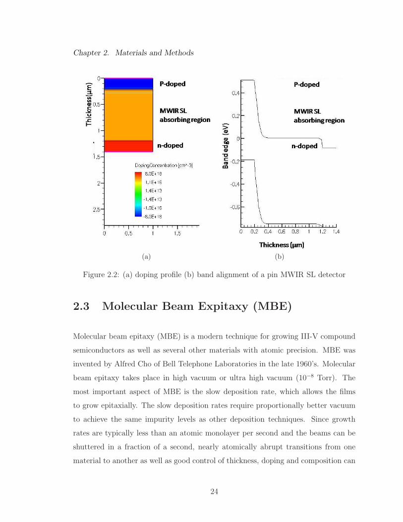
b. Sentaures Tcad software is used as a design tool to simulate different device
structures. Using this software structures are generated using the graphical
user interface which doping profiles and meshing strategies can also be defined.
Generated structures can be used as an input file to a program written by the
user to show electrical and optical characteristics. For SLs, band alignment
and dark current of different structures with different materials and doping
profiles are studied and simulated before designing the final structure. Figure
2.2(b) shows band alignment simulation of a pin MWIR SL detector which the
doping profile is shown in figure 2.2(a).
23
Chapter 2. Materials and Methods
(a) (b)
Figure 2.2: (a) doping profile (b) band alignment of a pin MWIR SL detector
2.3 Molecular Beam Expitaxy (MBE)
Molecular beam epitaxy (MBE) is a modern technique for growing III-V compound
semiconductors as well as several other materials with atomic precision. MBE was
invented by Alfred Cho of Bell Telephone Laboratories in the late 1960’s. Molecular
beam epitaxy takes place in high vacuum or ultra high vacuum (10−8 Torr). The
most important aspect of MBE is the slow deposition rate, which allows the films
to grow epitaxially. The slow deposition rates require proportionally better vacuum
to achieve the same impurity levels as other deposition techniques. Since growth
rates are typically less than an atomic monolayer per second and the beams can be
shuttered in a fraction of a second, nearly atomically abrupt transitions from one
material to another as well as good control of thickness, doping and composition can
24

Chapter 2. Materials and Methods
be realized. Structures presented in this work were grown in solid source VG-80 MBE
reactor, which consists of two identical growth chambers, preparation chamber and a
load lock. Load lock is used to take samples in and out of the preparation chamber.
To take out samples from the load lock, it must be vented to atmosphere, and to
put samples back to chamber it needs to be pumped down with a mechanical pump
and a turbo pump to vacuum (1 × 10⁻⁸ Torr). The preparation chamber is used
for substrate transfer, substrate storage and substrate heating for initial outgassing.
The preparation sample is equipped with a trolley system used to transfer samples
between the preparation and growth chambers. The preparation chamber is equipped
with an ion pump which allows to achieve pressure of ∼ 1× 10⁻¹⁰ Torr. Each of the
growth chambers hold UHV level (pressure ∼ 10−10 Torr) which are equipped with
an ion pump, a He closed loop cryopump and a Titanium sublimation pump. The
stainless steel shroud around the growth chamber is filled with Liquid Nitrogen (LN2)
which captures residual gases in the chamber. Growth chamber is also equipped with
the following: effusion cells, tools for in situ monitoring of growth process (Reflection
High Energy Electron Diffraction (RHEED) gun, pyrometer for measuring substrate
temperature and ion gauge for monitoring flux pressure during the growth process).
Also it contains residual gas analyzer to monitor pressure of residual gases such as
H2O, CO2, N2 and CO. A schematic of MBE growth chamber is shown in figure 2.3.
2.3.1 Growth of InAs/GaSb superlattice
In order to achieve high signal-to-noise ratio in the photodetector, the quality of
the SL interfaces has to be accurately controlled. In InAs/GaSb SL, two types of
interfaces form grown along the [001] growth direction, the “InSb-like” or “GaAs-like”
interface. The existence of these interfaces have been clearly shown by other research
groups using scanning tunneling microscopy [23, 24]. Since the lattice constant of
25
Chapter 2. Materials and Methods
Figure 2.3: Schematic of a Molecular Beam Epitaxy growth chamber
InSb (GaAs) is much larger (smaller) than that of the GaSb substrate, insertion
of a few monolayers of these materials leads to a large compressive (tensile) strain,
thereby dramatically changing the structural, optical and electrical properties of
the SL. Development of an optimized growth procedure for the strain-balanced SL
with well-ordered constituent and interfacial layers is critical for the realization of
a photodetector with a high absorption coefficient and reduced dark current. This
study is done for midwave regime by introducing Sb and As soak times before GaSb
and InAs respectively. The interface optimization for LWIR regime will be discussed
in chapter 3.
2.4 X-ray diffraction
X-ray scans are used to determine the structural properties of the SLs. Double crystal
X-ray diffraction (XRD) is a non-destructive technique for the structural characteri-
26

Chapter 2. Materials and Methods
zation of thin crystalline films. When an X-ray beam bombards a crystalline lattice
in a given orientation, the beam is scattered in a definite manner characterized by
the atomic structure of the lattice. X-ray diffraction, occurs when the wavelength
of X-rays and the interatomic distances in the lattice have the same order of mag-
nitude. X-rays diffracted from an ordered array of scattering centres can give rise
to interference maxima and minima. In order to observe x-ray diffraction from a
crystalline lattice, the Bragg condition (equation 2.1) must be satisfied. When the
waves are scattered from lattice planes separated by the interplanar distance d, the
scattered waves interfere constructively. The path difference between two waves un-
dergoing constructive interference is given by 2d sin θ, where θ is the scattering angle.
Therefore, Bragg’s law is given as following:
2dh,k,l sin θ = n.λ (2.1)
Where dh,k,l is the distance between the atom planes (h, k, l are the Miller indices),
θ is the incident angle, n is the order of diffraction and λ is X-ray wavelength.
Figure 2.4: Schematic diffraction of X-rays in the crystal
X-ray scans in this work were performed with a Philips double-crystal X-ray
diffractrometer using the Cu-Ka1 line.
A typical XRD spectrum from InAs/GaSb SL is presented in figure 2.5 .
27

Chapter 2. Materials and Methods
27 28 29 30 31 32 3310
100
1000
10000
100000
1000000
-2 +2
Cou
nts/s
FWHM 1st SL peak= 16 arcsec Period = 61.5 A
a/a = 0
GaSb, 0
+1-1
Figure 2.5: Typical XRD spectrum from InAs/GaSb SL
Parameters, which can be extracted from this spectrum, are:
a. Lattice constant of substrate and average lattice constant of the SL can be
obtained using the following equation:
a =nλ
2 sin θ(2.2)
Where n is equal to 1, λ is known and equal to 1.5406A, angle θ can be deter-
mined directly from the XRD spectrum. For the SL average lattice constant
angle θ is corresponding to SL zero order peak.
b. Strain relation between substrate and epilayer which can be found from the
following equation:
∆a
as=
ae − asas
=sin θe − sin θs
sin θs(2.3)
28

Chapter 2. Materials and Methods
Where as and ae correspond to the lattice constants of the substrate and the
epi-layer respectively.
c. Superlattice thickness can be achieved from different methods. One of the
methods proposed by Biefeld et al [25] is to calculate the superlattice period
P as:
P = 4Nd0 (2.4)
Where
N =nd
4(d0 − dn)(2.5)
here n is the diffraction order, d0(dn) is the distance between atomic planes
for different diffraction orders. For the SL presented in the figure 2.5 average
value of period was found to be 6.15 nm which is in good agreement with the
value extracted from the Bragg’s law.
The above method for the determination of SL period thickness can be formal-
ized and implemented as a computer program . Rocking curves presented in
this work were analyzed with an automated algorithm based on the dynamical
theory of diffraction (Bede RADs software).
d. Full-Width at Half-Maximum (FWHM) is a good qualitative measure of crys-
talline quality of the structure. Narrow and symmetrical SL peaks indicate
perfectly ordered structure with compositionally abrupt interfaces. On the
contrary, broad and asymmetrical satellite peaks indicate variation of period
thickness and growth defects accumulating at the interfaces of SL. Typically,
FWHM for the first satellite peak of SL is calculated.
29
Chapter 2. Materials and Methods
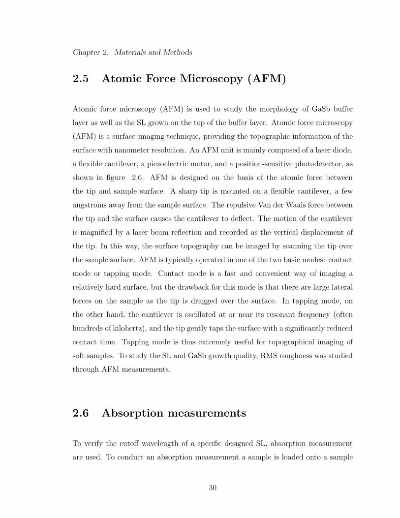
2.5 Atomic Force Microscopy (AFM)
Atomic force microscopy (AFM) is used to study the morphology of GaSb buffer
layer as well as the SL grown on the top of the buffer layer. Atomic force microscopy
(AFM) is a surface imaging technique, providing the topographic information of the
surface with nanometer resolution. An AFM unit is mainly composed of a laser diode,
a flexible cantilever, a piezoelectric motor, and a position-sensitive photodetector, as
shown in figure 2.6. AFM is designed on the basis of the atomic force between
the tip and sample surface. A sharp tip is mounted on a flexible cantilever, a few
angstroms away from the sample surface. The repulsive Van der Waals force between
the tip and the surface causes the cantilever to deflect. The motion of the cantilever
is magnified by a laser beam reflection and recorded as the vertical displacement of
the tip. In this way, the surface topography can be imaged by scanning the tip over
the sample surface. AFM is typically operated in one of the two basic modes: contact
mode or tapping mode. Contact mode is a fast and convenient way of imaging a
relatively hard surface, but the drawback for this mode is that there are large lateral
forces on the sample as the tip is dragged over the surface. In tapping mode, on
the other hand, the cantilever is oscillated at or near its resonant frequency (often
hundreds of kilohertz), and the tip gently taps the surface with a significantly reduced
contact time. Tapping mode is thus extremely useful for topographical imaging of
soft samples. To study the SL and GaSb growth quality, RMS roughness was studied
through AFM measurements.
2.6 Absorption measurements
To verify the cutoff wavelength of a specific designed SL, absorption measurement
are used. To conduct an absorption measurement a sample is loaded onto a sample
30

Chapter 2. Materials and Methods
Figure 2.6: Essential components of atomic force microscopy (AFM)
holder which is then loaded in the main compartment of the FTIR. Prior to this, a
background measurement is taken of either atmospheric conditions or the sample’s
substrate. The percent transmission is the ratio of the signal transmitted through the
sample and the background measurement signal multiplied by 100%. The absorption
is then computed as 100% - transmission.
The sample can either be loaded into a room temperature sample holder or a
liquid nitrogen cooled dewar. The room temperature sample holder is a simple
metalic stand with a hole in it. The sample is held in place over the hole with a
magnetic strip. The liquid nitrogen cooled dewar, as shown in figure 2.7, has a
normal incident sample holder, figure 2.7(c), and a Brewster angle sample holder,
figure 2.7(b). The samples are held in place using thermal grease or indium.
31

Chapter 2. Materials and Methods
Mirror
Light SourceMirror
DewarSample
Sample Compartment
Detector
Interferometer
(a)
(b) (c)
Figure 2.7: (a) Optical absorption measurement set-up, sample holder is loaded inthe main compartment of the FTIR (b) Brewster angle sample holder (c) Normalincidence sample holder
2.7 Processing
The next step after the growth of the material is the processing. For determining the
quality of FPA, single pixel devices are tested. The processing of single pixel detectors
are divided in to three steps of: top contact metalization, mesa isolation, and bottom
32
Chapter 2. Materials and Methods
contact metalization. Optical photolithography is a common step for formation of
top, bottom and mesa isolation. The typical steps in a photolithographic process
are: wafer cleaning, dehydration bake, adhesion promoter application, photoresist
application, soft bake, exposure and develop cycle. Wafers are cleaned consecutively
in acetone, isopropanol (IPA) and de-ionized (DI) water (5 minutes each) and then
blow dried with nitrogen (N2). After cleaning, dehydration bake is performed to
drive off most of the adsorbed water on the surface of the wafer. The dehydration
bake is for 6 minutes at 150 degrees. Immediately after the bake, the wafer was
primed with hexamethyldisilazane (HMDS), which acted as an adhesion promoter.
After applying HMDS, resist is applied at the top. For the top metalization positive
photoresist was spun on the wafer. After resist application, the wafer was baked
at 90 degrees for 90 seconds. The purpose of this step is to drive off most of the
solvents in the resist. After bake, the wafers are exposed with the mask aligner using
mask 1 as shown in figure 2.8(a). After the exposure the sample was baked, then
flood exposed again without the mask for resist reversal. After the final exposure,
the sample was developed leaving the photoresist in the desired places for metal
deposition. After photolithography, the metal contact is deposited. We used Ti (500
A)/Pt (500 A)/Au (3000 A) to achieve ohmic contact. The next step is the mesa
isolation etch. The photolithographic steps for the mesa isolation etch are similar
to the steps used for top contact metallization. First the sample is pretreated and
primed. Then positive resist was spun on and baked. Using Mask 2 in figure 2.8(b)
the sample was exposed on the mask aligner. After that samples are etched (it can be
both wet etched or dry etched) to the bottom contact layer. After the mesa isolation
etch, photoresist was applied as it was for the top contact metallization except Mask
3 in figure 2.8(c) was used. The bottom contact metal is Ti (500 A)/Pt (500 A)/Au
(3000 A) is then applied. Finally the sample is soaked in acetone for lift-off. The
final mesa size of a single-pixel device is 410 × 410 µm. To study the effect of
surface leakage current on the performance of a single pixel, devices with aperture
33

Chapter 2. Materials and Methods
(a) (b) (c)
Figure 2.8: Schematics of the masks used in fabrication process of the superlatticedetectors
diameters of 300, 200, 150, 100, 50 and 25 µm are fabricated. The schematic of the
fully processed single-pixel photodiode with contact metallization is shown in figure
2.9.
Top
Bottom
N-Contact
P-Contact
Absorber
Substrate
Figure 2.9: Conventionally processed pin diode
2.8 Characterization
After processing, devices were cleaved and wire-bonded to a leadless chip carrier
(LCC). To evaluate the electrical and optical performance of photodetectors the de-
34

Chapter 2. Materials and Methods
vice to be tested was placed in a close-cycle Helium cryostat. Bias dependent dark
Current-voltage measurements were performed using a semiconductor parameter an-
alyzer. The dark current was measured with a cold radiation shield, which was
painted black to avoid signals due to reflections. From the dark current measure-
ments, we can determine the dynamic resistance:
RdA = A
(
dI
dV
)
−1
(2.6)
where A is the mesa area, and the derivate is calculated from the measured dark
current. Spectral response measurements were performed on devices at temperatures
ranging from 50 K to 300 K using a Nicolet 670 Fourier transform infrared (FT-
IR) spectrometer and a Keithley 428 preamplifier. The FTIR contains a glow bar
source, a Michelson interferometer with a movable mirror, and internally mounted
Deuterated Triglycine Sulfate (DTGS) thermal detector. For the spectral response
measurement, the IR beam is directed outside of the FTIR off of a parabolic mirror
and onto the detector mounted in the close-cycle He cryostat. Relative spectral
response was obtained by dividing the photocurrent of the SL detectors with that
obtained using a calibrated DTGS thermal detector [26]. A schematic of the spectral
response is shown in figure 2.10.
The responsivity R of a photodiode characterizes its performance in terms of the
photocurrent generated per incident photon flux which is estimated using radiometry.
R =signal
Φe. (2.7)
Spectral responsivity of the detector is calculated by:
R(λ) = RmaxNR(λ) (2.8)
where (NR(λ)) is the normalized spectral response and multiplied by the peak re-
sponsivity (Rmax).
35

Chapter 2. Materials and Methods
Figure 2.10: Spectral response measurement setup
To measure reponsivity, infrared radiation from a black body source with con-
trollable temperature is directed through a chopper onto the SL detector mounted
inside the dewar. The electrical signal produced by the detector is then aplimfied
by a Keithley amplifier and measured using a network analyzer. The radiant power
from the blackbody can be calculated by:
Φe =
∫
∞
0
Me,λ(λ, T ).Abb.Adet
r2dλ (2.9)
Where Me,λ is the radiant existence, Abb is the area of the blackbody aperture, Adet
is the area of the detector and r is the distance from the blackbody to the detector.
A schematic of the responsivity setup is shown in figure 2.11.
The maximum responsivity can be calculated from:
I(Amps) =
∫ λcut
0
Me,λ(λ, T ).Abb.Adet
r2.NR(λ).Rmaxdλ. (2.10)
Solving for Rmax,
Rmax = dfracIAbb.Adet
r2.
∫ λcut
0
Me,λ(λ, T ).NR(λ)dλ (2.11)
36

Chapter 2. Materials and Methods
ChpperBlacobodySource
BlackbodyTemperatureController
ChopperController
Dewar
Current Amplifier
FFTNetworkAnalyzer
PC
Figure 2.11: Responsivity measurement setup
From Rmax quantum efficiency, other figure of merit of the detectors, can be
calculated,
η(λ) =RmaxNR(λ)hc
λq. (2.12)
Detectivity can be found using
D∗ =R(λ)
√Ad
in/√∆f
(2.13)
where in is the current noise measured by the spectrum analyzer when the black-
body is no longer incident on the detector and ∆f is given by
∆f =1
2τAV G(2.14)
where τAV G is the integration time of the measurement.
37
Chapter 2. Materials and Methods
2.9 Conclusion
In this chapter we discussed growth, processing and characterization of InAs/GaSb
SL infrared single-pixel detectors. Detailed description of characterization techniques
used in this work and their applications for structural, optical and electrical char-
acterization of as grown materials and processed devices were presented. Physical
foundations underlying X-ray diffraction, atomic force microscopy and transmission
measurements were discussed. Schematic of experimental set up used for spectral
response, transmission, and responsivity measurements were presented.
38

Chapter 3
Mid-wave and Long-wave pin and
nBn SL detectors
3.1 Introduction
In this chapter the design, growth, processing and characterization of single pixel
midwave pin InAs/GaSb SL detectors will be described. Next, longwave SL design
and growth optimiazation will be covered. Definition and advantages of the nBn
devices will be discussed. Growth, processing and characterization of single pixel
longwave pin and nBn InAs/GaSb SL detectors are also presented. I-V characteristics
and responsivity of the longwave nBn detector are compared with a pin photodiode
with the same absorber region structure. The nBn exhibits lower dark current density
than the pin diode at equivalent applied electric field. The unique processing of
the nBn detector and the consequent removal of the sidewall surface, as well as the
depletion region width shrinking result in lower dark current densities in nBn devices.
39

Chapter 3. Mid-wave and Long-wave pin and nBn SL detectors
3.2 Midwave superlattices (MW SLs)
3.2.1 Design and growth of MW SLs
8 MLs of InAs and 8 MLs of GaSb was used for all of the MW SL designs. Nextnano
simulations of this material system is shown in figure 3.1. As it is shown in figure
3.1(a) the electron wavefunction is defined in the InAs layer where as hole wave-
function is mostly confined to the GaSb layer. Figure 3.1(b) shows the dispersion
diagram for 8 MLs InAs/8 MLs GaSb at 0 K indicating a cut off wavelength of 4.6
µm.
3.2.2 Calibration of the group III elements for SL growth
Reflection high energy electron diffraction (RHEED) oscillations are used to calibrate
the group III cells during the MBE growth. For the purpose of exact growth rates
for the SL growths, a method proposed by Kaspi et al [27] was utilized for tuning
of group III sources. Two calibration samples with structures formed by different
binary III-V compounds (InAs and GaSb, AlSb and GaSb etc.) with different periods
were grown under the same growth conditions. Then from the spacing between the
satellite fringes in the scans, the exact growth rates can be determined by solving
the following system of equations ( 3.1 and 3.2),
rGa.tGa + rIn.tIn = T1 (3.1)
rGa.tGa + rIn.tIn = T2 (3.2)
where T1 and T2 are the SL periods determined from the (004) X-ray scan, rGa and
rIn are the growth rates of Ga and In, and tGa and tIn are the times of Ga and In
deposition, respectively.
40

Chapter 3. Mid-wave and Long-wave pin and nBn SL detectors
0 2 4
-0.6
-0.4
-0.2
0.0
0.2
0.4
0.6
0.8
1.0
Ener
gy (e
V)
Distance (nm)
Conduction Heavy hole Light hole
2.4 nm GaSb
2.4 nm InAs
0 K
(a)
0.0 0.2 0.4 0.6 0.8 1.0
-0.42-0.36-0.30-0.24-0.18-0.12-0.060.000.060.120.180.240.30
Ener
gy (e
V)
Kz(x /L)
Conduction Band Heavy Hole Band Light Hole Band
0 K-Midwave
(b)
Figure 3.1: (a) electron and hole wavefunctions (b) dispersion diagram at 0 K for2.4 nm GaSb/2.4 nm InAs.
This method is illustrated in figure 3.2 for In and Ga sources. One calibra-
tion sample with 50 periods of 8ML InAs/8ML GaSb SL and 50 periods of 8ML
InAs/12ML GaSb SL was grown on GaSb substrate. Symmetric (004) X-ray scans
were performed on the samples with a Philips double-crystal X-ray diffractometer
and growth rates were determined as rGa = 0.48 ML/s and rIn = 0.29 ML/s.
41

Chapter 3. Mid-wave and Long-wave pin and nBn SL detectors
28 29 30 31 32 331
FWHM 2=79 arcsec
a/a1= -0.127%
a/a2= -0.078%
coun
ts/s
/2 , O
0
First +1First -1
Second +1Second -1
FWHM 1=48.9 arcsec
Figure 3.2: Estimation of the growth rates by X-ray scan of SLs width differentperiod
3.2.3 MW SL growth optimization
As mentioned in the previous chapter, interfaces are one of the key elements in the
growth of the SLs. Growth of MW SLs has been previously developed in our group
and 2 seconds of As before 8 MLs of InAs layer and 12 seconds of Sb before 8 MLs
of GaSb layer provide the optimum interface conditions for the MW SLs. Figure
3.3 shows the shutter sequence used for th MW SLs. More details on the MW SL
growth conditions can be found in [28].
3.3 Midwave pin InAs/GaSb SL detector
3.3.1 Growth
All of the structures in this chapter were grown on Te-doped epi-ready (100) GaSb
substrates. The structure consisted of a 360 nm thick bottom contact layer formed by
42
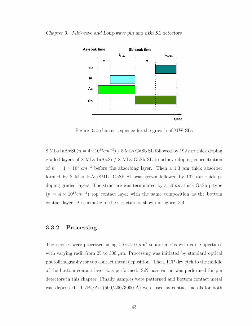
Chapter 3. Mid-wave and Long-wave pin and nBn SL detectors
Sb
As
In
Sb-soak timeAs-soak timetInAs tGaSb
t,sec
Ga
Figure 3.3: shutter sequence for the growth of MW SLs
8 MLs InAs:Si (n = 4×1018cm−3) / 8 MLs GaSb SL followed by 192 nm thick doping
graded layers of 8 MLs InAs:Si / 8 MLs GaSb SL to achieve doping concentration
of n = 1 × 1017cm−3 before the absorbing layer. Then a 1.3 µm thick absorber
formed by 8 MLs InAs/8MLs GaSb SL was grown followed by 192 nm thick p-
doping graded layers. The structure was terminated by a 50 nm thick GaSb p-type
(p = 4 × 1018cm−3) top contact layer with the same composition as the bottom
contact layer. A schematic of the structure is shown in figure 3.4
3.3.2 Processing
The devices were processed using 410×410 µm2 square mesas with circle apertures
with varying radii from 25 to 300 µm. Processing was initiated by standard optical
photolithography for top contact metal deposition. Then, ICP dry etch to the middle
of the bottom contact layer was performed. SiN passivation was performed for pin
detectors in this chapter. Finally, samples were patterned and bottom contact metal
was deposited. Ti/Pt/Au (500/500/3000 A) were used as contact metals for both
43
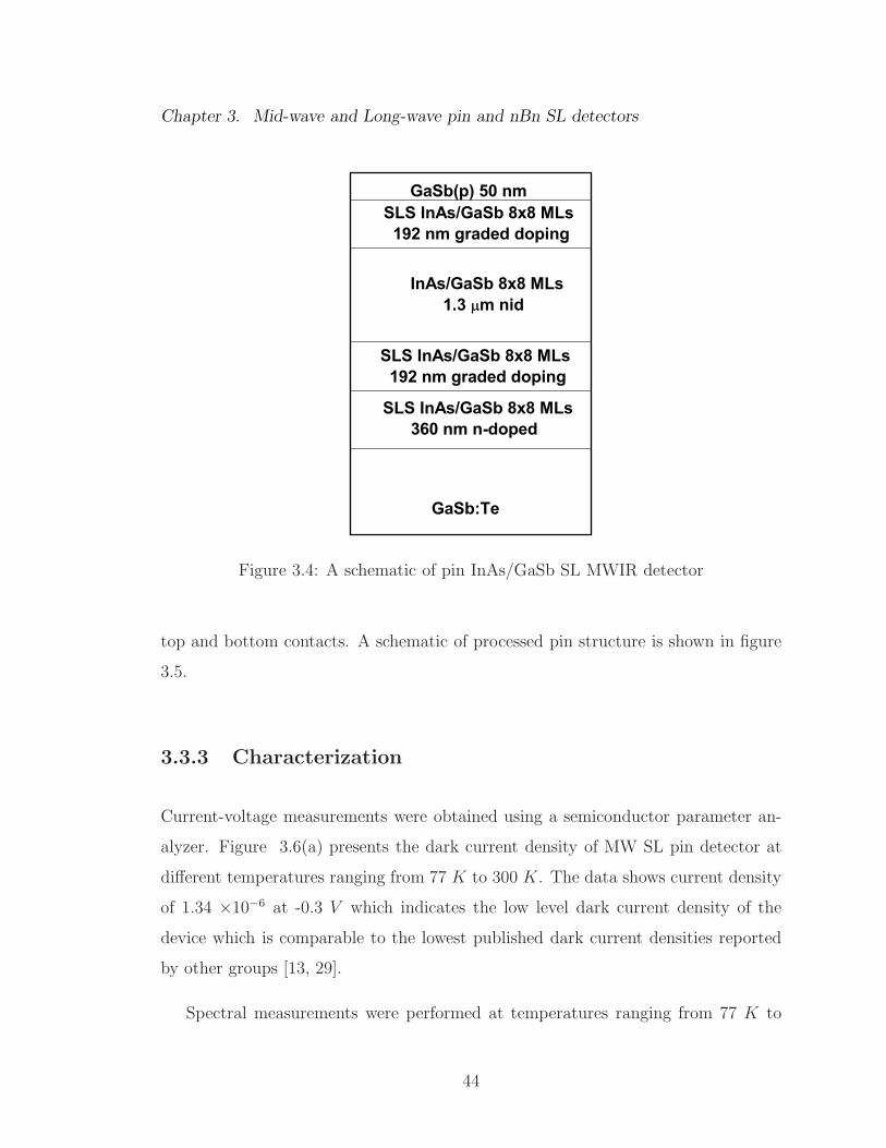
Chapter 3. Mid-wave and Long-wave pin and nBn SL detectors
SLS InAs/GaSb 8x8 MLs 192 nm graded doping
GaSb:Te
SLS InAs/GaSb 8x8 MLs 360 nm n-doped
SLS InAs/GaSb 8x8 MLs 192 nm graded doping
InAs/GaSb 8x8 MLs 1.3 m nid
GaSb(p) 50 nm
Figure 3.4: A schematic of pin InAs/GaSb SL MWIR detector
top and bottom contacts. A schematic of processed pin structure is shown in figure
3.5.
3.3.3 Characterization
Current-voltage measurements were obtained using a semiconductor parameter an-
alyzer. Figure 3.6(a) presents the dark current density of MW SL pin detector at
different temperatures ranging from 77 K to 300 K. The data shows current density
of 1.34 ×10⁻⁶ at -0.3 V which indicates the low level dark current density of the
device which is comparable to the lowest published dark current densities reported
by other groups [13, 29].
Spectral measurements were performed at temperatures ranging from 77 K to
44
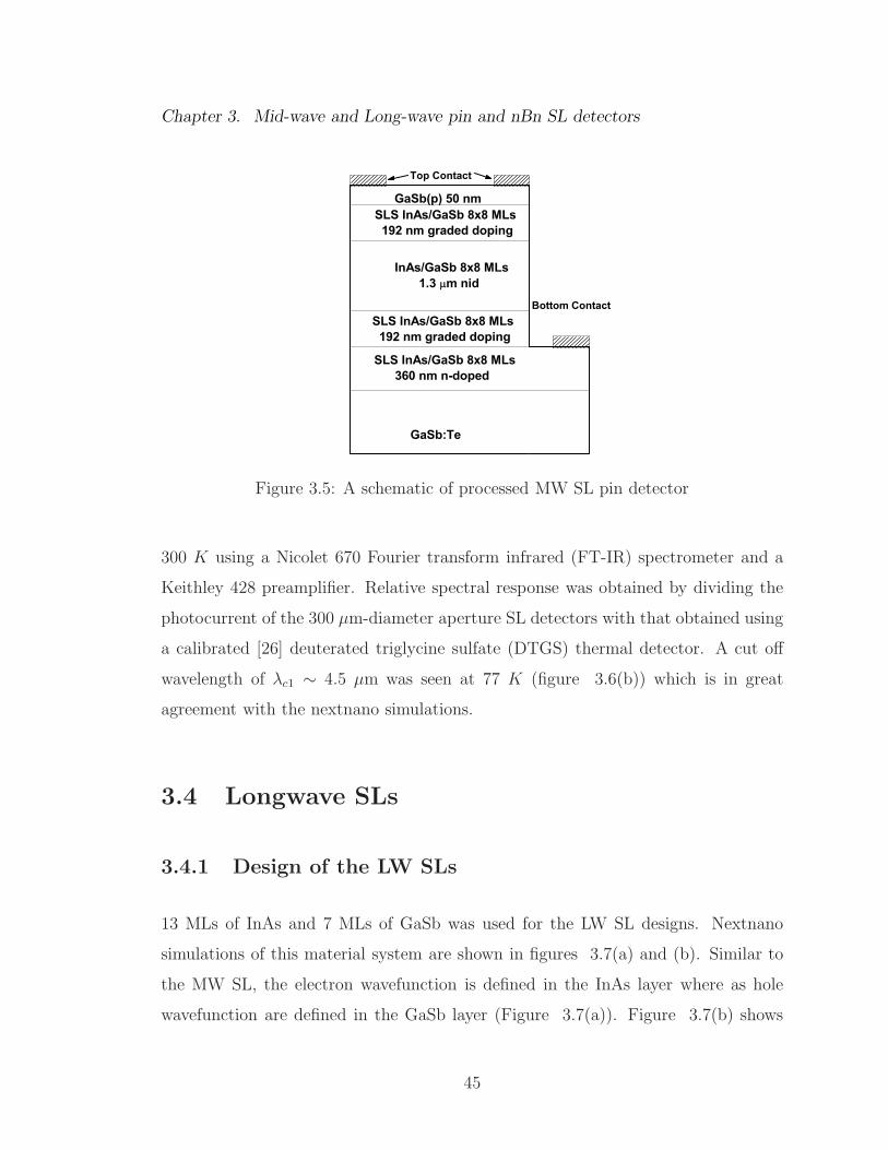
Chapter 3. Mid-wave and Long-wave pin and nBn SL detectors
Bottom Contact
SLS InAs/GaSb 8x8 MLs 192 nm graded doping
GaSb:Te
SLS InAs/GaSb 8x8 MLs 360 nm n-doped
SLS InAs/GaSb 8x8 MLs 192 nm graded doping
InAs/GaSb 8x8 MLs 1.3 m nid
GaSb(p) 50 nm
Top Contact
Figure 3.5: A schematic of processed MW SL pin detector
300 K using a Nicolet 670 Fourier transform infrared (FT-IR) spectrometer and a
Keithley 428 preamplifier. Relative spectral response was obtained by dividing the
photocurrent of the 300 µm-diameter aperture SL detectors with that obtained using
a calibrated [26] deuterated triglycine sulfate (DTGS) thermal detector. A cut off
wavelength of λc1 ∼ 4.5 µm was seen at 77 K (figure 3.6(b)) which is in great
agreement with the nextnano simulations.
3.4 Longwave SLs
3.4.1 Design of the LW SLs
13 MLs of InAs and 7 MLs of GaSb was used for the LW SL designs. Nextnano
simulations of this material system are shown in figures 3.7(a) and (b). Similar to
the MW SL, the electron wavefunction is defined in the InAs layer where as hole
wavefunction are defined in the GaSb layer (Figure 3.7(a)). Figure 3.7(b) shows
45

Chapter 3. Mid-wave and Long-wave pin and nBn SL detectors
-3 -2 -1 0 1 2 31E-8
1E-7
1E-6
1E-5
1E-4
1E-3
0.01
0.1
1
10
100
Cur
rent
den
sity
(A/C
m2 )
Bias (V)
77K 100K 150K 200K 250K 300K
(a)
2 3 4 5 6 70
2
4
6
Spe
ctra
l Res
pons
e (a
.u.)
Wavelength ( m)
77K 100K 150K 200K
0.5 V
(b)
Figure 3.6: (a) Dark current density, and (b) spectral response of MWIR pin SLdetector
the dispersion diagram for 13 MLs InAs/7 MLs GaSb at 0 K which indicates a cut
off wavelength of 7.48 µm. Since InAs is -0.6% lattice mismatched to GaSb, InSb
is used as strain compensating layer which shifts the cutoff wavelength to 8.3 µm
(figures 3.8(a) and (b)).
46

Chapter 3. Mid-wave and Long-wave pin and nBn SL detectors
0 2 4 6
-0.6
-0.4
-0.2
0.0
0.2
0.4
0.6
0.8
1.0
Ene
rgy
(eV
)
Distance (nm)
Conduction Heavy hole Light hole
7 ML GaSb
13 ML InAs
(a)
0.0 0.2 0.4 0.6 0.8 1.0-0.48
-0.40
-0.32
-0.24
-0.16
-0.08
0.00
0.08
0.16
Ene
rgy
(eV
)
Kz(x /L)
Conduction Band Heavy Hole Band Light Hole Band
0 K
(b)
Figure 3.7: (a) band alignment, and electron/hole wavefunctions (b) dispersion dia-gram of 13 MLs of InAs and 7 MLs of GaSb
Optical absorption in semiconductor materials is proportional to the overlap be-
tween the of electron and hole wavefunctions which is described as following:
α ∝ |〈Φe | Φh〉|2 = |∫
SLperiod
Φe.Φ∗
hdr|2 (3.3)
Where Φe and Φh refer to the electron and hole wavefunctions, respectively. When
the InAs layer thickness is increased to extend the cutoff wavelength of the SLs into
47
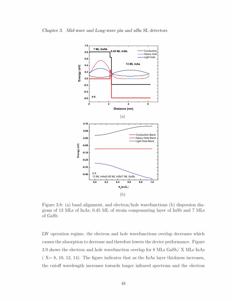
Chapter 3. Mid-wave and Long-wave pin and nBn SL detectors
0 2 4 6
-0.6
-0.4
-0.2
0.0
0.2
0.4
0.6
0.8
1.0
Ener
gy (e
V)
Distance (nm)
Conduction Heavy hole Light hole
7 ML GaSb
13 ML InAs
0.45 ML InSb
0 K
(a)
0.0 0.2 0.4 0.6 0.8 1.0
-0.40
-0.32
-0.24
-0.16
-0.08
0.00
0.08
0.16
Ener
gy (e
V)
Kz(x /L)
Conduction Band Heavy Hole Band Light Hole Band
0 K13 ML InAs/0.45 ML InSb/7 ML GaSb
(b)
Figure 3.8: (a) band alignment, and electron/hole wavefunctions (b) dispersion dia-gram of 13 MLs of InAs, 0.45 ML of strain compensating layer of InSb and 7 MLsof GaSb
LW operation regime, the electron and hole wavefunctions overlap decreases which
causes the absorption to decrease and therefore lowers the device performance. Figure
3.9 shows the electron and hole wavefunction overlap for 8 MLs GaSb/ X MLs InAs
( X= 8, 10, 12, 14). The figure indicates that as the InAs layer thickness increases,
the cutoff wavelength increases towards longer infrared spectrum and the electron
48
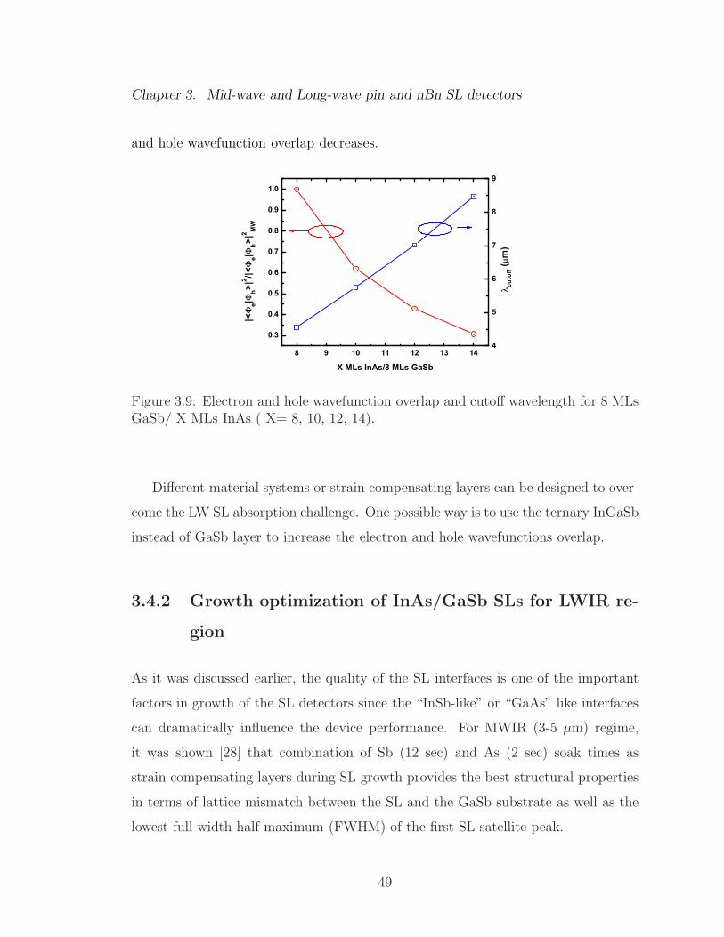
Chapter 3. Mid-wave and Long-wave pin and nBn SL detectors
and hole wavefunction overlap decreases.
8 9 10 11 12 13 14
0.3
0.4
0.5
0.6
0.7
0.8
0.9
1.0
|<e|
h>|2 /|<
e|h>|
2 MW
X MLs InAs/8 MLs GaSb
4
5
6
7
8
9
cuto
ff (
m)
Figure 3.9: Electron and hole wavefunction overlap and cutoff wavelength for 8 MLsGaSb/ X MLs InAs ( X= 8, 10, 12, 14).
Different material systems or strain compensating layers can be designed to over-
come the LW SL absorption challenge. One possible way is to use the ternary InGaSb
instead of GaSb layer to increase the electron and hole wavefunctions overlap.
3.4.2 Growth optimization of InAs/GaSb SLs for LWIR re-
gion
As it was discussed earlier, the quality of the SL interfaces is one of the important
factors in growth of the SL detectors since the “InSb-like” or “GaAs” like interfaces
can dramatically influence the device performance. For MWIR (3-5 µm) regime,
it was shown [28] that combination of Sb (12 sec) and As (2 sec) soak times as
strain compensating layers during SL growth provides the best structural properties
in terms of lattice mismatch between the SL and the GaSb substrate as well as the
lowest full width half maximum (FWHM) of the first SL satellite peak.
49

Chapter 3. Mid-wave and Long-wave pin and nBn SL detectors
In this section, the influence of the thickness of the InSb layer formed at the
GaSb-on-InAs interface and the growth temperature on the structural and optical
quality of type-II InAs/GaSb SL designed to operate in LWIR range is discussed.
To optimize the growth of strain-balanced SL, two methods were undertaken.
In the first approach, an InSb layer was intentionally grown between the binary
compounds in each SL period to suppress the natural tensile strain of the InAs
layer on GaSb-layer [30]. In second approach, the strain compensation was achieved
by forming “InSb-like” interfaces on InAs layers using an “Sb soak” that enabled
preferential group V exchange on the growth front. Structural quality of this material
was studied using high resolution X-ray diffraction (HRXRD) and cross sectional
scanning transmission electron microscopy (STEM) whereas surface morphology and
optical quality was assessed by atomic force microscopy (AFM) and Fourier transform
infrared (FTIR) spectroscopy, respectively.
Experimental procedure
All of the structures presented in this study were grown on n-type (Te-doped with n
∼ 5× 1017cm−3) epi-ready GaSb (001) double side polished substrates. Indium and
gallium growth rates were determined by monitoring intensity oscillations in the re-
flected high-energy electron diffraction (RHEED) patterns and were set to 0.5 ML/s
for Ga (which corresponds to the beam equivalent pressure (BEP) of 1.46×10⁻⁷ Torr)
and 0.45 ML/sec for In (which corresponds to the BEP of 2.5× 10⁻⁷ Torr). Group-
V fluxes were adjusted using a conventional ion gauge to satisfy group V/III BEP
flux ratio equal to 7.5 for GaSb and 3.8 for InAs. All the growths were performed
on cleaved 10×10 mm2 pieces of GaSb:Te substrate. The substrates were initially
outgassed in vacuum, and the surface oxide was then removed at high (535◦C) tem-
perature under Sb flux. The temperature of (1×3) to (2×5) reconstruction transition
(Tt) on GaSb surface observed on the RHEED pattern was taken as a reference for
50

Chapter 3. Mid-wave and Long-wave pin and nBn SL detectors
all the growth temperatures (figure 3.10). This transition temperature is the same
for all the GaSb substrates under given Sb flux [31].
Prior to the interface study, two samples with 8MLs InAs/ 8MLs GaSb and
8MLs InAs/ 24 MLs GaSb and the same thickness (0.144 µm) were grown on GaSb
substrates to verify the growth rates. From the spacing between the satellite fringes
in symmetric (004) X-ray scans, the exact growth rates of the InAs and GaSb layers
were determined [27].
(a) 3×pattern (b) 5×pattern
Figure 3.10: The temperature of (1×3) to (2×5) reconstruction transition was takenas a reference for the growth temperatures.
Epitaxial growth of strain-balanced SL
For the purpose of strain optimization in LWIR SL structure, two sets of samples
with 60 periods of SL with the same composition (13 MLs InAs/ 7 MLs GaSb) and
different methods of InSb interface formation were investigated.
Set A includes four SL samples with variable thickness (0, 0.45, 0.9 and 1.35
ML) of InSb layer inserted between InAs and GaSb layers. Set B includes three SL
51
Chapter 3. Mid-wave and Long-wave pin and nBn SL detectors
samples grown with ”InSb-like” interfaces formed by Sb-to-As exchange on GaSb-
on-InAs interface through the inclusion of variable Sb soak times (16, 18 and 20
sec) in the shutter sequence [32]. Since it was recently shown [28] that combination
of Sb and As soak times during SL growth provides additional flexibility in control
of average strain in the structure, we included a fixed As soak time (2 sec) in the
shutter sequence during the growth of set B. It should be noted that both sets of the
samples studied here were grown at 45 degrees below the Tt.
The bandgap of all of the samples was determined through room temperature
absorption measurements, which were performed using a Nicolet-870 Nexus Fourier
transform infrared (FTIR) spectrometer and the reflectivity module associated with
it. The reflectance of sample was calculated as ratio of reflected signals measured
from sample and reference substrate (n-type GaSb). In order to eliminate the trans-
mission component from the consideration, a thin layer of gold (50 nm) was deposited
on the backside of both the sample and the reference substrate. Thus, the absorbance,
A, as a function of wavelength is calculated using A = (1 - R) relation, where R is the
measured two pass reflectance of the sample. No significant changes in absorbance
were observed with the variation of growth procedure of SL. The cut-off wavelength
(defined as the wavelength where the response went to zero) was found to be ∼ 8µm
(at 300K).
Full width at half maximum (FWHM) for the first-order peak of SL as well as
lattice mismatch between zero-order peak of SL and GaSb substrate were calculated
for both sets and are presented in figures 3.11(a) and (b). It should be noted that SL
grown without any interfacial control has a FWHM of first order SL peak equal to
343 arcsecs and lattice mismatch between zero-order peak of SL and GaSb-substrate
of + 0.09% (tensile strain). This implies poor crystalline quality and fluctuations in
the thickness of the period due to, probably, anion exchange on SL interfaces during
the SL growth.
52

Chapter 3. Mid-wave and Long-wave pin and nBn SL detectors
-0.2 0.0 0.2 0.4 0.6 0.8 1.0 1.2 1.40
50
100
150
200
250
300
350
0.0
0.1
0.2
0.3
0.4
0.5
0.6
0.7
FWH
M o
f 1st
ord
er s
atel
lite
peak
(arc
sec)
InSb thickness, ML
a/a|, %
(a)
16 17 18 19 203032343638404244464850525456
0.0
0.2
0.4
0.6
FW
HM
of 1
st o
rder
sat
ellit
e pe
ak (a
rcse
c)
a/a|, %
Sb soak time, sec(b)
Figure 3.11: Growth optimization for LWIR structure using (a) InSb layer (b) groupV soak time.
In set A, with presence of 0.45 ML thick InSb layer in each SL period, the lattice
mismatch and FWHM of first order SL peak improves, reaching - 0.07% and 40
arcseconds, respectively. However, with further increase in InSb layer thickness,
structural quality of SL degrades (Figure 3.11(a)). We attribute this degradation to
53
Chapter 3. Mid-wave and Long-wave pin and nBn SL detectors
the possible change in growth mode from layer-by-layer (InSb thickness of 0.45 ML)
to the 3D island formation (InSb thickness exceeds 0.45 ML). In set B, the thickness
of ”InSb-like” interfaces is formed by controlling the duration of Sb soak-time. Based
on the MWIR InAs/GaSb SL optimization [28] and due to 13 MLs thickness of InAs
layer in the LWIR SL, we used 18 seconds of Sb soak time which was used as a base
line for the study. Figure 3.11(b) indicates that the FWHM of first order SL peak and
lattice mismatch of SL to the substrate does not change significantly with increase
in the Sb soak time. This can be explained by the fact that Sb-for-As exchange on
the InAs surface during Sb-soak is thermodynamically less favorable than the As
for Sb exchange. It is evident, that both the above mentioned approaches did not
lead to totally ”strain-balanced” SL material. However, the SL grown with the 0.45
ML InSb layer inserted in every period of SL possesses the lowest value of lattice
mismatch to the substrate (- 0.07%) and FWHM of the first order SL satellite peak
(40 arcsec). Therefore, this growth procedure is undertaken for the further studies.
Optimum growth temperature
Using the optimum thickness of InSb (0.45 ML) as strain compensation layer, we grew
another set of samples to study the optimum growth temperature. The temperature
dependent surface diffusion of the ad-atoms affects the structural and optical prop-
erties of the SL. It is necessary to have a substrate temperature high enough to avoid
excessive element V deposition, but low enough to limit the atom exchanges at the
different interfaces.
This set (C) includes three samples with 60 periods of 13 ML InAs/ 0.45 ML
InSb/ 7 ML GaSb SL structure grown at 25, 45 and 65 degrees below Tt. FWHM
of first order SL peak as well as lattice mismatch of zero-order peak of SL and
GaSb-substrate were calculated for this set and are presented in figure 3.12. The
data indicates a clear minimum at 45 below the Tt, with 40 arcsec FWHM and -
54

Chapter 3. Mid-wave and Long-wave pin and nBn SL detectors
0.07% (compressive strain) lattice mismatch. The - 0.07% compressive strain can be
further compensated by combination of ”GaAs-like” (formed by As-to-Sb exchange
on InAs-on-GaSb interface) and InSb interfaces.
-70 -60 -50 -40 -30 0 5
39
42
45
48
51
54
57
60
0.06
0.07
0.08
0.09
0.10
0.11
0.12
FWH
M o
f 1st
ord
er s
atel
lite
peak
(arc
sec)
Growth temperature -Tt (C)
I
a/aI
(%)
Tt
Figure 3.12: Growth temperature optimization for LWIR structure
To complete the structural investigations on the three sets of samples, the surface
morphology and roughness was assessed by AFM on a 5× 5µm2 scan area. For the
set A, 0.9 ML of InSb showed the lowest averaged roughness with a value equal to
0.15 nm. For the sets B and C the lowest averaged roughness was equal to 0.15 nm
for Sb soak-time of 18 sec, and 0.13 nm for the SL grown at (Tt - 65◦ ), respectively.
nBn based detector structure grown with optimized SL
After verifying the structural and optical properties of the superlattice, an n-B-n
infrared photodetector was grown. More detailed description of nBn detector will
be provided in the next section In order to compensate for the residual compressive
strain, a combination of ”GaAs-like” interface (formed by using one second of As
soak time) and InSb interface was used. The absorption region of detector consisted
55

Chapter 3. Mid-wave and Long-wave pin and nBn SL detectors
of 625 periods of [1sec As-soak time/13 ML InAs/0.45 ML InSb/ 7 ML GaSb] SL with
total thickness of ∼ 2µm. The top and bottom contact layers were formed by the
same SL with Si-doped (n = 4×1018cm−3) InAs layers and thickness of 0.13 µm and
0.47 µm, respectively. The HRXRD along with the heterostructure schematic of the
detector is shown in figures 3.13(a) and (b). The HRXRD exhibits intense satellite
peaks with a FWHM of the first-order peak equal to 16 arcsec and lattice mismatch
of 0%, attesting the good crystalline quality of the layers and high reproducibility
rate in the SL period.
GaSb:Te 2"
SL As/13ML InAs/0.425 InSb/7ML GaSb (Si) 4E18 76 per.
SL As/13ML InAs/0.425 InSb/7ML GaSb 2 m
Al0.2GaSb 100nm
GaSb 20 nm
SL As/13ML InAs/0.425ML InSb/7ML GaSb (Si) 4E18 12 per
(a)
27 28 29 30 31 32 33
10
100
1000
10000
100000
+3+3
+2
Cou
nts/
s
GaSb substrate
+1-1
SLS zeroth order
(b)
Figure 3.13: LWIR nBn structure (b) XRD of LWIR nBn structure, almost zero %lattice mismatch between SL and GaSb substrate and 19 arcsec FWHM for the firstsatellite peak.
Finally, the quality of interfaces in the detector structure is studied by cross-
sectional STEM. Transmitted electron images were acquired at various magnifica-
tions in atomic number contrast mode (ZC) using a High-Angle Annular Dark-Field
(HAADF) detector. The dark field imaging allows the chemical identification of
the respective epilayers displaying periodic InAs/InSb/GaSb layers over the total SL
56
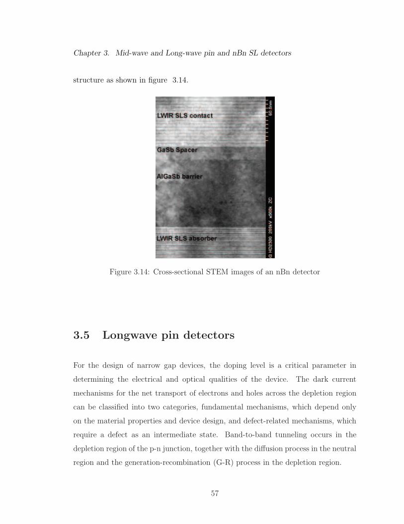
Chapter 3. Mid-wave and Long-wave pin and nBn SL detectors
structure as shown in figure 3.14.
Figure 3.14: Cross-sectional STEM images of an nBn detector
3.5 Longwave pin detectors
For the design of narrow gap devices, the doping level is a critical parameter in
determining the electrical and optical qualities of the device. The dark current
mechanisms for the net transport of electrons and holes across the depletion region
can be classified into two categories, fundamental mechanisms, which depend only
on the material properties and device design, and defect-related mechanisms, which
require a defect as an intermediate state. Band-to-band tunneling occurs in the
depletion region of the p-n junction, together with the diffusion process in the neutral
region and the generation-recombination (G-R) process in the depletion region.
57

Chapter 3. Mid-wave and Long-wave pin and nBn SL detectors
In this section a series of long wavelength InAs/GaSb pin diodes grown on n-
type GaSb substrates has been analyzed using current-voltage (I-V) and responsivity
measurements. The series contains of one non-intentionally doped pin diode, along
with two p-doped absorbing region pin diodes. Non-intentionally doped LWIR SL
system is a residually n-type system due to thicker layers of residually n-type InAs
layers as compared to the residually p-type GaSb layers. The dopant material and
its concentration is an important parameter in long-wave (LW) InAs/GaSb type-
II SL design and growth, that can affect the optical and electrical properties of
SLs structures. Beryllium (Be) doping the InAs layers is an effective method in
decreasing the dark current by lowering the diffusion, generation-recombination and
tunneling currents and increase the quantum efficiency of the device by switching
to high mobility minority electron concentration [33]. In this section, investigation
of LWIR pin detector and the influence of absorber p-doping on the optical and
electrical properties of the devices is presented.
3.5.1 LWIR InAs/GaSb pin diodes growth and processing
To study the influence of p-doping of the absorbing region of pin SL detectors on
the device performance, a set of three pin detectors were grown. To enable device
comparisons, all three samples had exact same thicknesses for the absorbing region.
Devices were grown on Te-doped epi-ready (100) GaSb substrates using a solid source
molecular beam epitaxy VG-80 system. The system was equipped with SUMO cells
for gallium and indium, a standard effusion cell for aluminum and cracker cells for
antimony and arsenic.
The designs consisted of a 473 nm thick bottom contact layer formed by 13 MLs
InAs:Si (n =4×1018cm−3)/ 0.75 ML InSb/ 7 MLs GaSb SL followed by 250 nm
thick doping graded layers of 13 MLs InAs:Si / 0.75 ML InSb/ 7 MLs GaSb SL to
58

Chapter 3. Mid-wave and Long-wave pin and nBn SL detectors
achieve doping concentration of n =1×1017cm−3 before the absorbing layer. Then
a 1.9 µm thick absorber formed by 13 MLs InAs/ 0.75 ML InSb/ 7 MLs GaSb SL
was grown followed by 250 nm thick p-doping graded layers. The structure was
terminated by a 125 nm thick p-type (p= 4×1018cm−3) top contact layer with the
same composition as the bottom contact layer. The absorber region doping level
was varied during the growth of the three pin detectors. The first sample, absorbing
region was non-intentionally doped. In second and third samples the doping of
the absorbing regions were Be:5×1015cm−3 and Be:1×1016cm−3, respectively. The
heterostructure schematic along with the HRXRD of the non-intentionally doped pin
are presented in figures 3.15(a) and (b), respectivley. The HRXRD exhibits intense
satellite peaks with a full-width at half maximum (FWHM) of the first-order peak
equal to 46.8 arcsec and a lattice mismatch of ∼0%, attesting to the good crystalline
quality of the layers and the high reproducibility rate in the SL period. The devices
were processed using the same procedure described in section 3.3.2.
3.5.2 Characterization of LWIR InAs/GaSb pin diodes
Figure 3.16 presents the dark current density of pin structures at 77 K.
The data shows that the dark current density of the pin detectors decreases with
p-doping the InAs layers in the absorbing region. The lowest dark current density
is associated with the sample which the Be doping concentration in InAs layers is
5×1015cm−3. In this comparison we neglect the effect of surface leakage currents
since all three pin samples were identically processed and passivated. The main dark
current components in these detectors are diffusion, generation-recombination and
tunneling current.
1
R0A=
1
(R0A)diff+
1
(R0A)G−R+
1
(R0A)tunn(3.4)
59
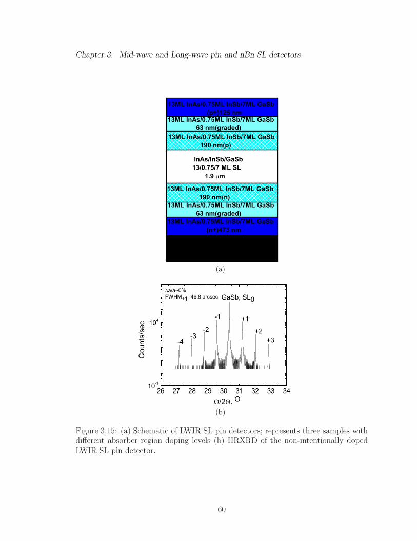
Chapter 3. Mid-wave and Long-wave pin and nBn SL detectors
GaSb:Te 2"
13ML InAs/0.75ML InSb/7ML GaSb (n+)473 nm
13ML InAs/0.75ML InSb/7ML GaSb 63 nm(graded)
13ML InAs/0.75ML InSb/7ML GaSb 190 nm(n)
InAs/InSb/GaSb 13/0.75/7 ML SL 1.9 m
13ML InAs/0.75ML InSb/7ML GaSb 190 nm(p)
13ML InAs/0.75ML InSb/7ML GaSb 63 nm(graded)
13ML InAs/0.75ML InSb/7ML GaSb (p+)125 nm
(a)
26 27 28 29 30 31 32 33 3410-1
104
/2 , O
Cou
nts/se
c
+2+3
-1
-2-3
-4
GaSb, SL0
+1
a/a~0%FWHM+1=46.8 arcsec
(b)
Figure 3.15: (a) Schematic of LWIR SL pin detectors; represents three samples withdifferent absorber region doping levels (b) HRXRD of the non-intentionally dopedLWIR SL pin detector.
60

Chapter 3. Mid-wave and Long-wave pin and nBn SL detectors
0.0 0.1 0.2 0.3 0.4 0.51E-3
0.01
0.1
1
10
Cur
rent
den
sity
(A/c
m2 )
Bias (V)
undoped 1E16 5E15
Figure 3.16: Dark current density at 77 K for the three pin structures.
Where R0A is the dynamic resistance at zero bias, and the thermal diffusion resis-
tance, (R0A)diff , is expressed as following:
(R0A)diff =(KT )1/2
q3/21
n2i
[
1
NA(µe
τe)1/2 tanh(
dpLe
) +1
ND(µh
τh)1/2 tanh(
dnLh
)
]
−1
(3.5)
Where ni is the intrinsic carrier density, k is the Boltzman constant, τe,h is the
electron (hole) lifetime, q is the electric charge, NA,D is the acceptor (donor) concen-
tration, and T is the temperature, dP,N is the region thickness of the carrier, and Le,h
is the diffusion length of the electrons and holes. So as the doping level increases,
R0A increases which lowers the dark current associated with diffusion mechanism.
So, the thermal diffusion current is associated with the minority carriers within a
diffusion length of the depletion region. As the doping level increases, the minority
carrier concentration decreases, therefore the diffusion current decreases.
R0A associated with Generation-Recombination mechanism is described as fol-
lowing:
(R0A)G−R =2VBi
qniW(τG−R) (3.6)
61

Chapter 3. Mid-wave and Long-wave pin and nBn SL detectors
Where τG−R is the effective G-R lifetime and W is the depletion region with at zero
bias voltage. As the doping is increased, depletion width decreases, and therefore,
dark current associated with G-R is suppressed.
R0A associated with band to band tunneling is described as following [33]:
(R0A)tunn =4π2h2
q3E(Eg,100%
2m∗
)1/2exp
(
4Eg,100%
3qh
√
ǫsm∗N−1red
)
(3.7)
Where E is the electric field, ǫs is the static dielectric constant of the SLs, m∗
is the electron effective mass, Eg, 100% is the cutoff of the photodiode at 77 K and
Nred is the reduced carrier concentration and is, Nred = [1/NA + 1/ND]−1. From the
above expression, as the carrier concentration increases, the band to band tunneling
increases as well.
As the doping in a pn junction increases, the depletion region width decreases
which results in an increase in tunneling of the majority carriers across the depletion
region. Moreover, the decrease in depletion width causes an increase in electric field
across the space charge region that increases the tunneling probability furthermore.
Therefore, by increasing the doping level, diffusion current decreases. The G-
R current also decreases due to decrease in depletion width. Tunneling current
decreases up to a certain doping concentration (5×1015cm−3 Be doped) but as the
doping concentration increases more, the maximum electric field across the depletion
region increases which causes the tunneling probability to increase. This can explain
the larger dark current for the 1×1016cm−3 Be doped sample compared to the n.i.d
sample at bias points larger than 0.35 V .
Responsivity and D∗ were measured at 77 K using a pourfill dewar and a Micron
M365 calibrated 800 K blackbody source. No anti-reflection coating was applied on
the devices. As is shown in figure 3.17(a), the responsivity of pin detectors increases
with 5×1015cm−3 Be doping of the photodiode absorbing region. Further increase
62

Chapter 3. Mid-wave and Long-wave pin and nBn SL detectors
in the doping concentration (1×1016cm−3) leads to a drop in responsitivity of pin
photodiodes. To understand this behavior qualitatively, it’s worth noticing that the
responsivity of a photodetector is the number of collected carriers per incident pho-
ton. Therefore, it is proportional to the ratio of photo-carriers leaving the absorbing
region and photo-carriers recombining within the absorbing region. When the ab-
sorption region is Be doped, the minority carriers switch to high mobility electrons
as compared to the non-intentiolly doped sample where the minority carriers are
holes. The rate that carriers leave the absorbing region is faster in Be doped samples
as compared to n.i.d sample. Therefore, the probability of carrier recombination
decreases and leads to higher responsivity. However, at higher Be doping concen-
trations (1×1016cm−3), mobility of minority carriers decreases due to the increase in
scattering from the dopants.
The shot-noise limited spectral detectivity (D∗) of the device was estimated using:
D∗ =R
√
2qJ + (4kT )/(RdAd)(3.8)
Where R is the responsivity, q is the electronic charge, T is the temperature of
the device, k is Boltzmann’s constant, J is the current density, Rd is the dynamic
resistance, and Ad is the diode area. Detectivity measurements for pin devices is
shown in figure 3.17(b). The behavior seen in figure 3.17(b) for detectivties of pin
devices is well expected since it is a measure of signal (responsivity) to noise (dark
current) ratio.
63
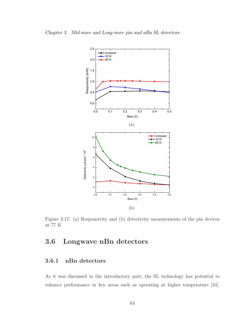
Chapter 3. Mid-wave and Long-wave pin and nBn SL detectors
0.0 0.1 0.2 0.3 0.4 0.5
0.0
0.5
1.0
1.5
2.0
2.5
Res
pons
ivity
(A/W
)
Bias (V)
Undoped 1E16 5E15
(a)
0.0 0.1 0.2 0.3 0.4 0.5
0
2
4
6
8
10
Det
ectiv
ity (J
ones
) * 1
09
Bias (V)
Undoped 1E16 5E15
(b)
Figure 3.17: (a) Responsivity and (b) detectivity measurements of the pin devicesat 77 K
3.6 Longwave nBn detectors
3.6.1 nBn detectors
As it was discussed in the introductory part, the SL technology has potential to
enhance performance in key areas such as operating at higher temperature [34].
64
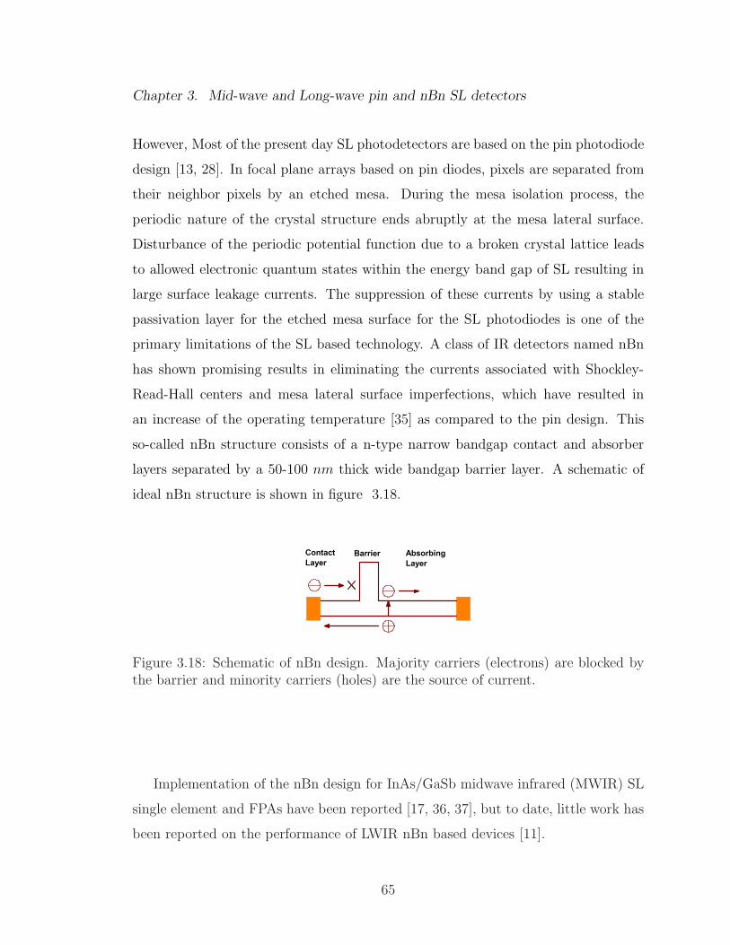
Chapter 3. Mid-wave and Long-wave pin and nBn SL detectors
However, Most of the present day SL photodetectors are based on the pin photodiode
design [13, 28]. In focal plane arrays based on pin diodes, pixels are separated from
their neighbor pixels by an etched mesa. During the mesa isolation process, the
periodic nature of the crystal structure ends abruptly at the mesa lateral surface.
Disturbance of the periodic potential function due to a broken crystal lattice leads
to allowed electronic quantum states within the energy band gap of SL resulting in
large surface leakage currents. The suppression of these currents by using a stable
passivation layer for the etched mesa surface for the SL photodiodes is one of the
primary limitations of the SL based technology. A class of IR detectors named nBn
has shown promising results in eliminating the currents associated with Shockley-
Read-Hall centers and mesa lateral surface imperfections, which have resulted in
an increase of the operating temperature [35] as compared to the pin design. This
so-called nBn structure consists of a n-type narrow bandgap contact and absorber
layers separated by a 50-100 nm thick wide bandgap barrier layer. A schematic of
ideal nBn structure is shown in figure 3.18.
Absorbing Layer
BarrierContact Layer
Figure 3.18: Schematic of nBn design. Majority carriers (electrons) are blocked bythe barrier and minority carriers (holes) are the source of current.
Implementation of the nBn design for InAs/GaSb midwave infrared (MWIR) SL
single element and FPAs have been reported [17, 36, 37], but to date, little work has
been reported on the performance of LWIR nBn based devices [11].
65
Chapter 3. Mid-wave and Long-wave pin and nBn SL detectors
Photoconductive gain in nBn detectors
In a photoconductor with ohmic contacts (injecting contacts), the photoconductor
exhibits photoconductive gain, which is defined as the ratio of the number of elec-
trons/holes collected in the external circuit to the number of absorbed photons. An
absorbed photon photogenerates an electron hole pair, which drift in opposite di-
rections. The electron drift velocity is larger than the hole drift velocity and hence
reaches the opposite contact first. The sample however must be electrically neutral
which means another electron must enter the sample from the negative electrode.
This new electron also drifts across quickly to reach the contact while the hole is still
drifting slowly across the sample. Thus another electron must enter the sample to
maintain neutrality, and so on, until either the hole reaches the negative electrode
or recombines with one of these electrons entering the sample. The external pho-
tocurrent therefore corresponds to the flow of many electrons per absorbed photon,
which leads to a photoconductive gain. The gain is also defined as the ratio of the
recombination lifetime to the transit time. For nBn detectors since no depletion
region exists, therefore the behavior of these devices is closer to that of photconduc-
tors than photodiodes. However, since for every photon absorbed, the electron is
blocked by the barrier and cannot reach the contact, thus nBn devices do not have
photoconductive gain. This has recently been shown by Klipstein [38].
3.6.2 Growth and processing of LWIR SL detector based on
nBn design
The detector consisted of a 380 nm bottom contact layer formed by 13 MLs InAs:Si
(n = 4×1018cm−3)/ 0.75 ML InSb/ 7 MLs GaSb SL. Then a 1.9 µm thick non-
intentionally doped (n.i.d.) absorber region formed by 13 MLs InAs/ 0.75 ML InSb/
7 MLs GaSb SL was grown followed by a 100 nm thick Al0.2Ga0.8Sb barrier layer.
66

Chapter 3. Mid-wave and Long-wave pin and nBn SL detectors
The Al0.2Ga0.8Sb barrier layer was capped with a 20 nm thick GaSb spacer to avoid
oxidation of the Al during the processing steps. The structure was terminated by a
125 nm thick n-type (n = 4×1018cm−3) top contact layer with the same composition
as the bottom contact layer. The heterostructure schematic along with the HRXRD
of the detector is shown in figure 3.19 3.19(a) and 3.19(b), respectively.
One of the advantages of the nBn structures is its unique processing technique
which eliminates surface currents. Unlike p-i-n diodes where each pixel is defined
with a deep etch (standard processing), in nBn processing (shallow etched devices),
the diffusion length in the absorber is the parameter that isolates one device from the
device next to it. This eliminates the presence of surface leakage currents. In order
to show the reduction of surface leakage currents in shallow etching as compared
to the deep etched processing, both methods were implemented on the LWIR nBn
structure. Specific processing used for the nBn structures is as follows.
The material was processed into normal incidence single pixel photodiodes with
apertures ranging from 25-300 µm in diameter using standard optical photolithogra-
phy technique. Processing was initiated with the formation of ohmic contacts to the
n-type top contact layer followed by etching of this contact layer to the top of the
barrier ( ∼ 125 nm) for the mesa definition. Using this approach, the active layer
was encapsulated by the barrier and there was no need for development of an ad-
ditional passivation coating. We used inductively coupled plasma (ICP) etching for
this purpose. Then part of the wafer was masked with the photoresist and the ICP
deep dry etching to the middle of the bottom n-type contact layer was performed on
the other part. An ohmic contact was evaporate. An ohmic contact was evaporated
on the bottom contact layer. We used a Ti (50 nm)/Pt (50 nm) /Au (300 nm) as
n-contact metal for both top and bottom contacts.
Figure 3.20 shows the main processing steps which are used for nBn devices to
make both shallow and deep devices.
67

Chapter 3. Mid-wave and Long-wave pin and nBn SL detectors
GaSb, 20 nm
GaSb:Te 2"
13ML InAs/0.75ML InSb/7ML GaSb (n+)380 nm
InAs/InSb/GaSb 13/0.75/7 ML SL (nid)1.9 m
Al0.2GaSb 100 nm
13ML InAs/0.75ML InSb/7ML GaSb (n+)125 nm
(a)
27 28 29 30 31 32 331
10
100
1000
10000
-3
-2
-1
+3
+2coun
ts/s
/2 , O
FWHM+1=36 arcseca/a= -0.05 %
+1
GaSb
Al0.2GaSb
(b)
Figure 3.19: (a) Structure schematic (b) HRXRD of the LWIR nBn detector.
Figures 3.21(a) and (b) present schematic of a completed shallow etched, and
deep etched devices, respectively.
68

Chapter 3. Mid-wave and Long-wave pin and nBn SL detectors
Figure 3.20: Main processing steps for LWIR nBn detectors
3.6.3 Characterization of the LWIR SL detector based on
nBn design
Figure 3.22 shows the dark current density for shallow etched and deep etched
processed nBn devices. A reduction of the dark current density in shallow etched
device can be seen at in comparison with the deep etched device. This is attributed
to the reduction of leakage surface currents.
Responsivity and detectivity of LWIR SL detectors based on nBn design is mea-
sured in the same as the LWIR SL pin detectors discussed in the previous chapter.
Figure 3.23(a) and (b) shows the responsivity and detectivity of the shallow etched
nBn device.
69

Chapter 3. Mid-wave and Long-wave pin and nBn SL detectors
(a) (b)
(c)
Figure 3.21: (a) Shallow etch processing (b) deep etch processing (c) shallow etchprocessing with indication of diffusion lengths.
3.7 Comparison of the LWIR pin and nBn detec-
tors
In this section device characteristics comparison between the LWIR pin devices pre-
sented in section 3.5 and the shallow etched nBn device presented in section is
presented.
• Processing:
Processing of both types of the devices is discussed in the earlier sections.
70

Chapter 3. Mid-wave and Long-wave pin and nBn SL detectors
0.0 0.5 1.0 1.5 2.01E-3
0.01
0.1
1
10
Dar
k cu
rren
t den
sity
(A/c
m2 )
|Vapplied| (V)
Shallow etched nBn Deep etched nBn
77 K
Figure 3.22: Dark current density of shallow, and deep etched nBn devices vs tem-perature. This comparison shows the effect of dark current density reduction due toreduction of surface leakage currents.
The only difference is that in pin devices one device is separated from the
neighboring device by the mesa etching which creates side walls exposing to
the atmosphere and results in presence of surface leakage current as a dark
current mechanism in the device. However, in nBn designs one device is defined
from the neighboring device by the diffusion length of the minority carriers.
Therefore, it allows for a shallow etch process that helps to reduce the surface
leakage currents.
• Spectral response:
The relative spectral responses of pin and nBn structures as a function of
wavelength are shown in figures 3.24(a) and (b), respectively. The data clearly
shows cutoff wavelength of λc ≈ 8 µm for both pin and nBn designs. The only
difference is that forward bias in nBn design is defined where negative bias is
applied on the top of device and reverse bias in pin design is defined where
negative bias is applied on the top of device.
71
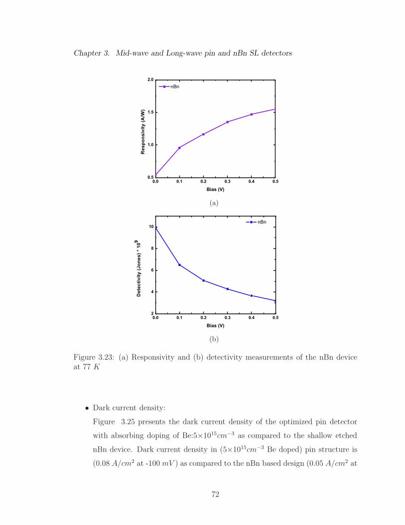
Chapter 3. Mid-wave and Long-wave pin and nBn SL detectors
0.0 0.1 0.2 0.3 0.4 0.50.5
1.0
1.5
2.0
Res
pons
ivity
(A/W
)
Bias (V)
nBn
(a)
0.0 0.1 0.2 0.3 0.4 0.52
4
6
8
10
Det
ectiv
ity (J
ones
) * 1
09
Bias (V)
nBn
(b)
Figure 3.23: (a) Responsivity and (b) detectivity measurements of the nBn deviceat 77 K
• Dark current density:
Figure 3.25 presents the dark current density of the optimized pin detector
with absorbing doping of Be:5×1015cm−3 as compared to the shallow etched
nBn device. Dark current density in (5×1015cm−3 Be doped) pin structure is
(0.08 A/cm2 at -100 mV ) as compared to the nBn based design (0.05 A/cm2 at
72

Chapter 3. Mid-wave and Long-wave pin and nBn SL detectors
4 6 80.1
0.2
0.3
0.4
0.5
0.6
0.7
Negative bias
Spe
ctra
l res
pons
e (a
.u)
Wavelength ( m)
77 K 125 K
(a)
4 6 80.0
0.5
1.0
1.5
2.0
Negative bias
Spe
ctra
l res
pons
e (a
.u)
Wavelength ( m)
77 K 125 K
(b)
Figure 3.24: Spectral response of (a) pin (b) nBn structure, 8 µm cutoff wavelengthis shown in the two diagrams.
+100 mV ). It is worth mentioning that the dark current density measurements
of the nBn design were measured with a 300 K background while the pin
dark current density measurements are performed with a cold shield which
can further decrease the dark current density associated with nBn devices.
This lower dark current density in nBn design is due to a reduction of the
73

Chapter 3. Mid-wave and Long-wave pin and nBn SL detectors
currents associated with Shockley-Read-Hall centers and mesa lateral surface
imperfections in nBn design. However, nBn structure, could also have lateral
diffusion of minority carriers (holes), which is ignored in this analysis [39].
0.0 0.5 1.0 1.5 2.01E-3
0.01
0.1
1
10
Cur
rent
den
sity
(A/c
m2 )
|Bias (V)|
5E15 cm-3
nBn
Figure 3.25: Dark current density at 77 K for nBn and pin structures
• Responsivity:
Figure 3.26(a) and (b) present the responsivity and detectivity of the optimized
pin detector with absorbing region doping of Be:5×1015cm−3 as compared to
the shallow etched nBn device, respectively.
Figure 3.26(a), shows that nBn device has a higher responsivity as compared
to the pin devices. Photodiodes based on nBn design eliminate SRH recom-
bination centers associated with depletion regions which are the main source
of recombination mechanisms in pin photodiodes, and therefore, more carriers
are extracted from the absorbing region which increases the responsivity of
these devices. It is worth mentioning that the responsivity of nBn devices can
be improved further with optimizing the barrier band offsets and thickness of
these structures.
74

Chapter 3. Mid-wave and Long-wave pin and nBn SL detectors
0.0 0.1 0.2 0.3 0.4 0.5
0.0
0.5
1.0
1.5
2.0
2.5
Res
pons
ivity
(A/W
)
Bias (V)
5E15 cm-3
nBn
(a)
0.0 0.1 0.2 0.3 0.4 0.50
2
4
6
8
10
Det
ectiv
ity (J
ones
) * 1
09
Bias (V)
nBn
5E15 cm-3
(b)
Figure 3.26: (a) Responsivity and (b) detectivity measurements of the pin and nBndevices at 77 K; nBn structure has the highest responsivity and detectivity valuesas compared to the pin structure.
Figure 3.26(b) shows that the nBn device has the higher detectivity as com-
pared to the pin device which is well expected since it is a measure of signal
(responsivity) to noise (dark current) ratio. Table I, shows summarized values
of dark current, responsivity and detectivity of pin and nBn devices.
75
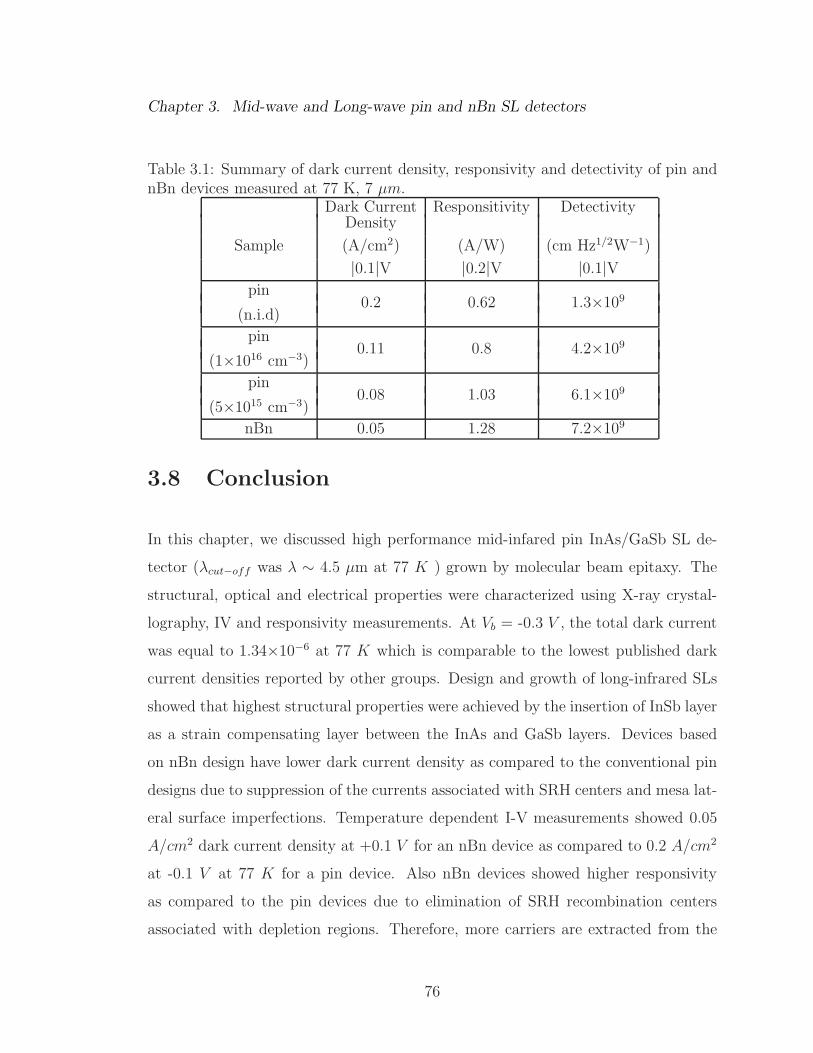
Chapter 3. Mid-wave and Long-wave pin and nBn SL detectors
Table 3.1: Summary of dark current density, responsivity and detectivity of pin andnBn devices measured at 77 K, 7 µm.
Dark Current Responsitivity DetectivityDensity
Sample (A/cm2) (A/W) (cm Hz1/2W−1)
|0.1|V |0.2|V |0.1|Vpin
0.2 0.62 1.3×10⁹(n.i.d)
pin0.11 0.8 4.2×10⁹
(1×1016 cm−3)
pin0.08 1.03 6.1×10⁹
(5×1015 cm−3)
nBn 0.05 1.28 7.2×10⁹
3.8 Conclusion
In this chapter, we discussed high performance mid-infared pin InAs/GaSb SL de-
tector (λcut−off was λ ∼ 4.5 µm at 77 K ) grown by molecular beam epitaxy. The
structural, optical and electrical properties were characterized using X-ray crystal-
lography, IV and responsivity measurements. At Vb = -0.3 V , the total dark current
was equal to 1.34×10⁻⁶ at 77 K which is comparable to the lowest published dark
current densities reported by other groups. Design and growth of long-infrared SLs
showed that highest structural properties were achieved by the insertion of InSb layer
as a strain compensating layer between the InAs and GaSb layers. Devices based
on nBn design have lower dark current density as compared to the conventional pin
designs due to suppression of the currents associated with SRH centers and mesa lat-
eral surface imperfections. Temperature dependent I-V measurements showed 0.05
A/cm2 dark current density at +0.1 V for an nBn device as compared to 0.2 A/cm2
at -0.1 V at 77 K for a pin device. Also nBn devices showed higher responsivity
as compared to the pin devices due to elimination of SRH recombination centers
associated with depletion regions. Therefore, more carriers are extracted from the
76

Chapter 3. Mid-wave and Long-wave pin and nBn SL detectors
absorbing region which increases the responsivity of the nBn devices. It is worth
mentioning that optical and electrical performance of both pin and nBn devices can
be improved by detailed passivation study for pin and optimized barrier and absorber
doping level as well as barrier material and composition for nBn devices.
77

Chapter 4
Dual Band nBn InAs/Ga(In)Sb SL
detectors
4.1 Introduction
In this chapter, for the first time the multi-spectral properties of infrared photode-
tectors based on type II InAs/Ga(In)Sb using an nBn heterostructure design are
shown. The optical and electrical properties of the MWIR and LWIR absorbing
layers are characterized using spectral response and current-voltage measurements,
respectively. Present day two color SL detector require two contacts per pixel lead-
ing to a complicated processing scheme and expensive specific ROICs. For the first
time, the dual-band response is achieved by changing the polarity of applied bias
using single contact processing. The spectral response shows a significant change
in the LWIR to MWIR ratio within a very small bias range (∼100 mV ) making it
compatible with commercially available read out integrated circuits (ROICs).
78

Chapter 4. Dual Band nBn InAs/Ga(In)Sb SL detectors
4.2 Background and applications of Bi-color in-
frared detectors
Multicolor detectors are desirable in a variety of IR applications related to remote
sensing and object identification. Today’s state-of-the-art multispectral imagers use
special optical and mechanical components like, e.g., filter wheels, beamsplitters
and lenses in order to spectrally separate and focus the radiation onto one or more
monospectral IR FPAs or even separate cameras [40]. These systems, due to their
technical complexity, are difficult to manufacture (and thus expensive) and difficult to
handle. Moreover, the images generated by these systems have an inherent temporal
and spatial registration problem. These problems and limitations can be overcome
by real multispectral FPA which have been under development during the last few
years.
The first approach to build multispectral imagers are FPAs operating at two
different spectral ranges, either in two separate atmospheric windows (“dual-band”)
or within one atmospheric window (“dual-color”). Dual-band detectors simply offer
the advantage that the pros of both infrared bands can be combined in one imager.
For example, MWIR imagers exhibit smaller blur spot for longer ranges and better
performance in hot humid areas, whereas LWIR imagers deliver better performance
in case of stray light or when the object under investigation is close to hot sources.
A dual-band imager can be used in a wider range of ambient conditions. Moreover,
dual-band detection permits the spectral discrimination of unique object features
and thus a better distinction between targets and background clutter due to specific
emissivity features.
Dual band, MWIR and LWIR, detectors have also interesting applications such
as computed-tomography imaging spectrometer (CTIS) [41].
79
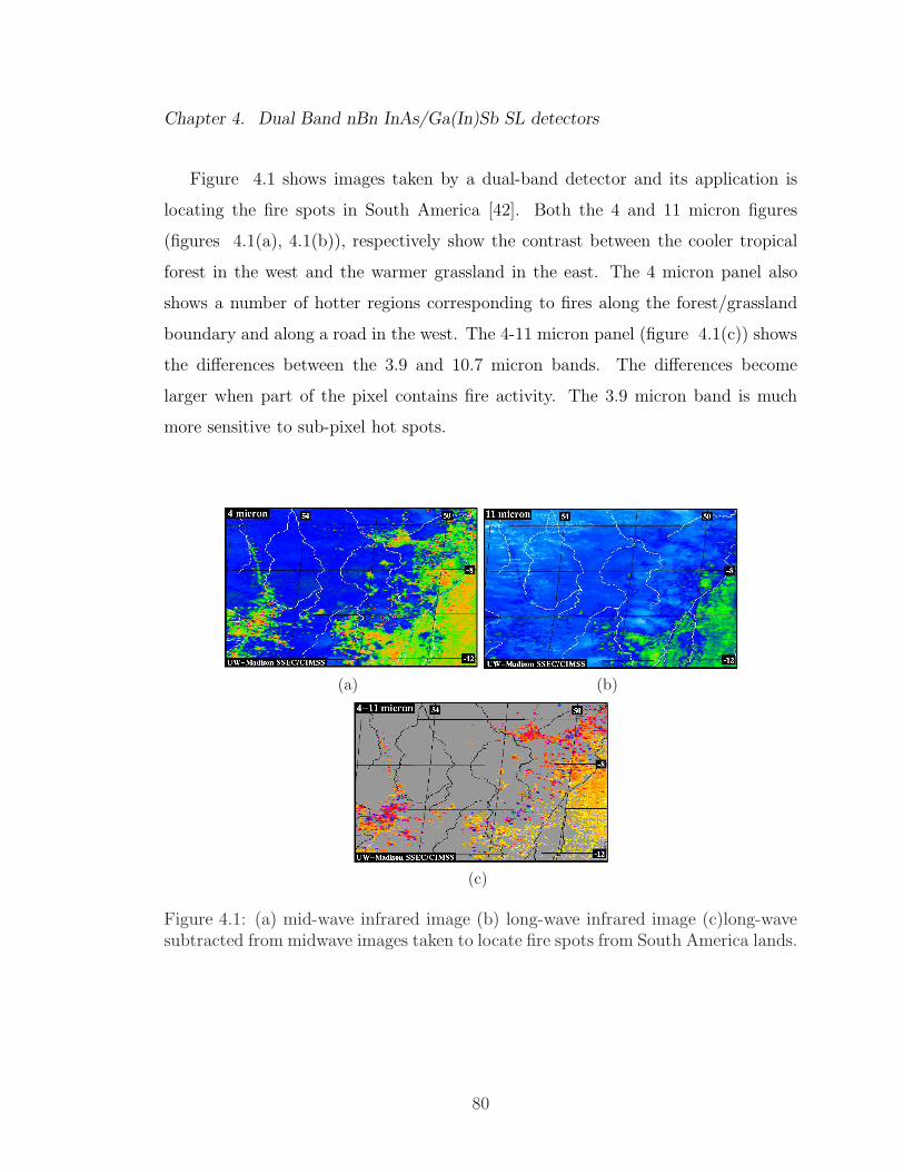
Chapter 4. Dual Band nBn InAs/Ga(In)Sb SL detectors
Figure 4.1 shows images taken by a dual-band detector and its application is
locating the fire spots in South America [42]. Both the 4 and 11 micron figures
(figures 4.1(a), 4.1(b)), respectively show the contrast between the cooler tropical
forest in the west and the warmer grassland in the east. The 4 micron panel also
shows a number of hotter regions corresponding to fires along the forest/grassland
boundary and along a road in the west. The 4-11 micron panel (figure 4.1(c)) shows
the differences between the 3.9 and 10.7 micron bands. The differences become
larger when part of the pixel contains fire activity. The 3.9 micron band is much
more sensitive to sub-pixel hot spots.
(a) (b)
(c)
Figure 4.1: (a) mid-wave infrared image (b) long-wave infrared image (c)long-wavesubtracted from midwave images taken to locate fire spots from South America lands.
80

Chapter 4. Dual Band nBn InAs/Ga(In)Sb SL detectors
4.3 Present bicolor detectors
Multicolor capabilities have been demonstrated with MCT and QWIP and more
recently in the SL system [43]. Present day two color SL detector require two contacts
per pixel leading to a complicated processing scheme and expensive specific ROICs.
Below are two examples of common bi-color infrared detectors.
• Illustrated in figure 4.2(a) shows a crosssection schematic of a 30-µm unit-
cell, single-mesa, single-contact dual-color detector, in addition to the typical
current-voltage (I-V) characteristic for this detector design, figure 4.2(b). The
two-color MCT architecture [44] leaves the p+ layer floating, and the polarity
of the voltage bias at the single pixel contact selects the spectral sensitivity
by reverse-biasing the p-n junction of interest. The CdTe/HgTe alloy compo-
sition or x value of the n-type absorber layers determines the spectral cutoff
characteristics of the detector in both detection bands. A positive (negative)
operating bias voltage at the pixel contact with respect to the FPA common-
ground contact provides reverse bias to the Band 2 (Band 1) p-n junction
while forward biasing the Band 1 (Band 2) p-n junction for detection of longer
(shorter) wavelength radiation.
Bi-color detectors based on HgCdTe are difficult to grow due to the strong
dependency of the bandgap on the alloy composition. Slight variations of the
growth temperature and the temperature non-uniformity across the CdZnTe
substrates result in different alloy compositions and a shift of the cut-off wave-
length over the FPA. Also, using back to back diodes to achieve the multicolor
detectors increases the complexity and therefore, the cost of the associated
ROICs.
• The two color SL detector structure ([43]) along with fully processed SL-FPA
SEM picture are shown in figures 4.3(a) and 4.3(b), respectively.
81
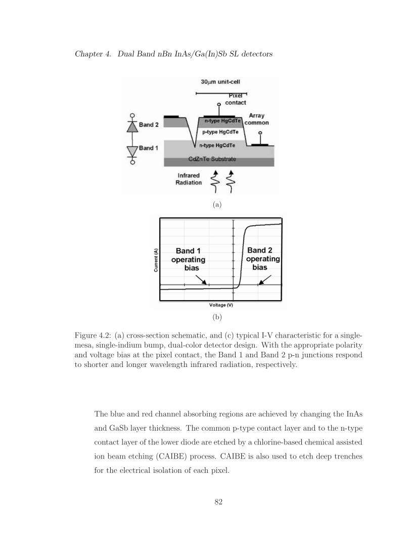
Chapter 4. Dual Band nBn InAs/Ga(In)Sb SL detectors
(a)
(b)
Figure 4.2: (a) cross-section schematic, and (c) typical I-V characteristic for a single-mesa, single-indium bump, dual-color detector design. With the appropriate polarityand voltage bias at the pixel contact, the Band 1 and Band 2 p-n junctions respondto shorter and longer wavelength infrared radiation, respectively.
The blue and red channel absorbing regions are achieved by changing the InAs
and GaSb layer thickness. The common p-type contact layer and to the n-type
contact layer of the lower diode are etched by a chlorine-based chemical assisted
ion beam etching (CAIBE) process. CAIBE is also used to etch deep trenches
for the electrical isolation of each pixel.
82

Chapter 4. Dual Band nBn InAs/Ga(In)Sb SL detectors
Red channel absorbing region
GaSb
n-type GaSb
Blue channel absorbing region
p-type GaSb/ common ground contact
n-type InAs
(a) (b)
Figure 4.3: (a) Schematic (b) SEM picture of two-color InAs/GaSb superlatticedetector
This two color SL FPA is based on two back to back diodes which has two
disadvantages of high cost ROICs associated with this specific design. Also,
two contacts per pixel leads to a complicated processing scheme.
In next section, we present a bias dependent dual band SL detector operating in the
MWIR and LWIR region. One of the advantages of this design is that it is compatible
with the standard single bump per contact processing, which reduces the cost and
complexity associated with the fabrication process.
4.4 Epitaxial growth and fabrication of dual-color
nBn SL detectors
To study the devices with type II InAs/(In)GaSb SL absorbers based on nBn design,
we grew two samples, referred to structures A and B. Both structures A and B
83
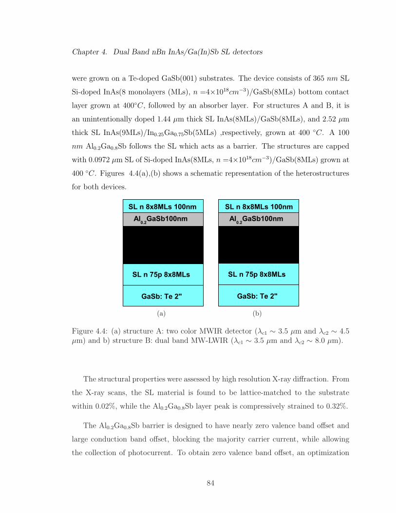
Chapter 4. Dual Band nBn InAs/Ga(In)Sb SL detectors
were grown on a Te-doped GaSb(001) substrates. The device consists of 365 nm SL
Si-doped InAs(8 monolayers (MLs), n =4×1018cm−3)/GaSb(8MLs) bottom contact
layer grown at 400◦C, followed by an absorber layer. For structures A and B, it is
an unintentionally doped 1.44 µm thick SL InAs(8MLs)/GaSb(8MLs), and 2.52 µm
thick SL InAs(9MLs)/In0.25Ga0.75Sb(5MLs) ,respectively, grown at 400 ◦C. A 100
nm Al0.2Ga0.8Sb follows the SL which acts as a barrier. The structures are capped
with 0.0972 µm SL of Si-doped InAs(8MLs, n =4×1018cm−3)/GaSb(8MLs) grown at
400 ◦C. Figures 4.4(a),(b) shows a schematic representation of the heterostructures
for both devices.
SLS nid 300p 8x8 MLs
SLS n 20P 8x8MLs
SL n 8x8MLs 100nm
SL n 75p 8x8MLs
GaSb: Te 2"
SL nid 300p 8x8 MLs 8MLs InAs x 8MLs InGaSb
Al0.2GaSb100nm
(a)
SLS nid 300p 8x8 MLs
SLS n 20P 8x8MLs
SL n 8x8MLs 100nm
SL n 75p 8x8MLs
GaSb: Te 2"
SL nid 300p 8x8 MLs 9MLs InAs x 5MLs InGaSb
Al0.2GaSb100nm
(b)
Figure 4.4: (a) structure A: two color MWIR detector (λc1 ∼ 3.5 µm and λc2 ∼ 4.5µm) and b) structure B: dual band MW-LWIR (λc1 ∼ 3.5 µm and λc2 ∼ 8.0 µm).
The structural properties were assessed by high resolution X-ray diffraction. From
the X-ray scans, the SL material is found to be lattice-matched to the substrate
within 0.02%, while the Al0.2Ga0.8Sb layer peak is compressively strained to 0.32%.
The Al0.2Ga0.8Sb barrier is designed to have nearly zero valence band offset and
large conduction band offset, blocking the majority carrier current, while allowing
the collection of photocurrent. To obtain zero valence band offset, an optimization
84
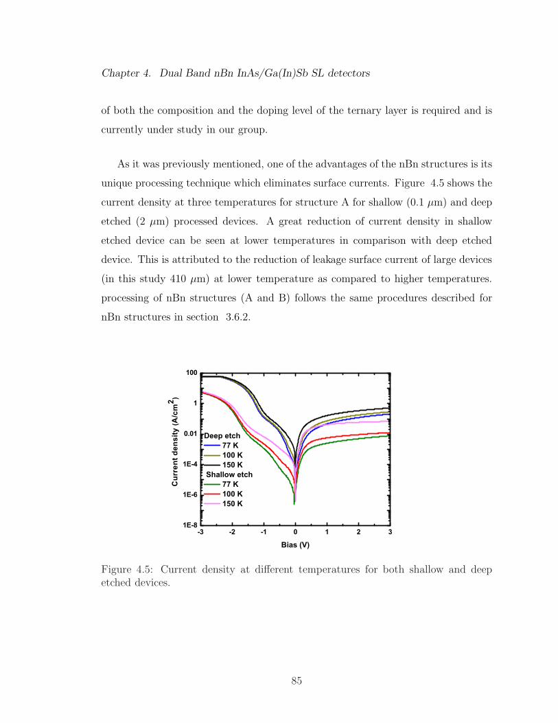
Chapter 4. Dual Band nBn InAs/Ga(In)Sb SL detectors
of both the composition and the doping level of the ternary layer is required and is
currently under study in our group.
As it was previously mentioned, one of the advantages of the nBn structures is its
unique processing technique which eliminates surface currents. Figure 4.5 shows the
current density at three temperatures for structure A for shallow (0.1 µm) and deep
etched (2 µm) processed devices. A great reduction of current density in shallow
etched device can be seen at lower temperatures in comparison with deep etched
device. This is attributed to the reduction of leakage surface current of large devices
(in this study 410 µm) at lower temperature as compared to higher temperatures.
processing of nBn structures (A and B) follows the same procedures described for
nBn structures in section 3.6.2.
-3 -2 -1 0 1 2 31E-8
1E-6
1E-4
0.01
1
100
Cur
rent
den
sity
(A/c
m2 )
Bias (V)
Deep etch 77 K 100 K 150 K
Shallow etch 77 K 100 K 150 K
Figure 4.5: Current density at different temperatures for both shallow and deepetched devices.
85

Chapter 4. Dual Band nBn InAs/Ga(In)Sb SL detectors
4.5 Device characterization: results and discus-
sions
Figures 4.6(a), and (b) present the dark current density of structures A and B at
temperatures ranging from 77K to 300 K. The data shows that dark current density
is higher in forward bias regime (positive voltage applied on the bottom contact).
We attribute this to the position of Al0.2Ga0.8Sb barrier. From the band alignment,
it is clear that the AlGaSb barrier is more effective in reducing the current in the
reverse bias (defined as negative voltage on the bottom contact).
The normalized relative spectral responses of structures A and B as a function
of voltage bias are displayed in figures 4.7(a) and (b), respectively .
The data clearly show that the two color( λc1 ∼ 3.5 µm and λc2 4.5 µm ) and(
λc1 ∼ 3.5 µm and λc2 ∼ 8 µm ) at 100K and 150 K for A and B , respectively, can be
seen under different polarity. Under forward bias (figure 4.8(a)), the photocarriers
from the absorber are collected. Absorber layers are SL 8×8 MLs InAs/GaSb (λc2 ∼4.5 µm) and SL 9×5 MLs InAs/In0.25Ga0.75Sb (λc2 ∼ 8.0 µm) for structures A and B,
respectively. When the device is under reverse bias (figure 4.8(b)), the photocarriers
from the heavily n-doped top contact layer (SL InAs/GaSb 8×8 MLs) are collected
and the photocarriers from the absorber are blocked by the barrier. Heavily doped
InAs in 0.0972 µm InAs/GaSb SL of the top contact layer, results in a larger optical
bandgap due to the Moss-Burstein effect and is the source of the signal at the shorter
wavelength for both of the structures A and B. It is also important to mention that
reverse bias signal is (50-100 times) weaker than the forward bias signal, which is
consistent with the fact that the top contact layer is thinner and heavily doped in
comparison with the absorber. Thickness optimization of the top contact layer will
be studied to obtain a signal under reverse bias as strong as the signal from the
absorber under forward bias.
86

Chapter 4. Dual Band nBn InAs/Ga(In)Sb SL detectors
-3 -2 -1 0 1 2 31E-8
1E-6
1E-4
0.01
1
100
Cur
rent
den
sity
(A/c
m2 )
Bias (V)
100 K 150 K 250 KStructure A- MWIR
(a)
-3 -2 -1 0 1 2 31E-7
1E-5
1E-3
0.1
10
1000
100 150 250
Cur
rent
den
sity
(A/c
m2 )
Bias (V)
Structure B- LWIR
(b)
Figure 4.6: Current density at different temperatures for (a) structure A and (b)structure B.
Figure 4.9(a) shows responsivity and quantum efficiency versus wavelength for
structure A. The peak responsivity was found to be 0.835 A/W at 3.5 µm with Vb
= 0.5V . The responsivity and quantum efficiency at 4 µm was 0.74 A/W and 23%,
respectively. No Antireflection (AR) coating was applied on the device.
The spectral specific detectivity D∗(λ) was estimated using equation 3.8. Peak
87

Chapter 4. Dual Band nBn InAs/Ga(In)Sb SL detectors
2.0 2.5 3.0 3.5 4.0 4.5 5.00.0
0.2
0.4
0.6
0.8
1.0
Nor
mal
ized
spe
ctra
l res
pons
e (a
.u.)
Wavelength ( m)
100 K 150 K
Vb= -1 V
Vb= 1 V
(a)
1 2 3 4 5 6 7 8 9 10 110.0
0.2
0.4
0.6
0.8
1.0
Vb= 0.9 volts
Nor
mal
ized
spe
ctra
l res
pons
e (a
.u.)
Wavelength ( m)
100 K 150 K
Vb= -0.7 volts
(b)
Figure 4.7: Spectral response of structure (a) A and (b) B at different temperaturesunder forward bias and reverse ;Vbis the applied voltage to the device.
D∗ was estimated to be 2.8×10¹¹cmHz1/2/W at 4 µm at Vb = 0.5 V .
The responsivity and quantum efficiency were also measured for structure B using
the same setup as for structure A. The external quantum efficiency was calculated
to be 12% and D∗ was calculated to be 2.5×10¹⁰cmHz1/2/W at 5.5 µm. The peak
responsivity was 0.51 A/W also at 5.5 µm. The responsivity and quantum efficiency
88
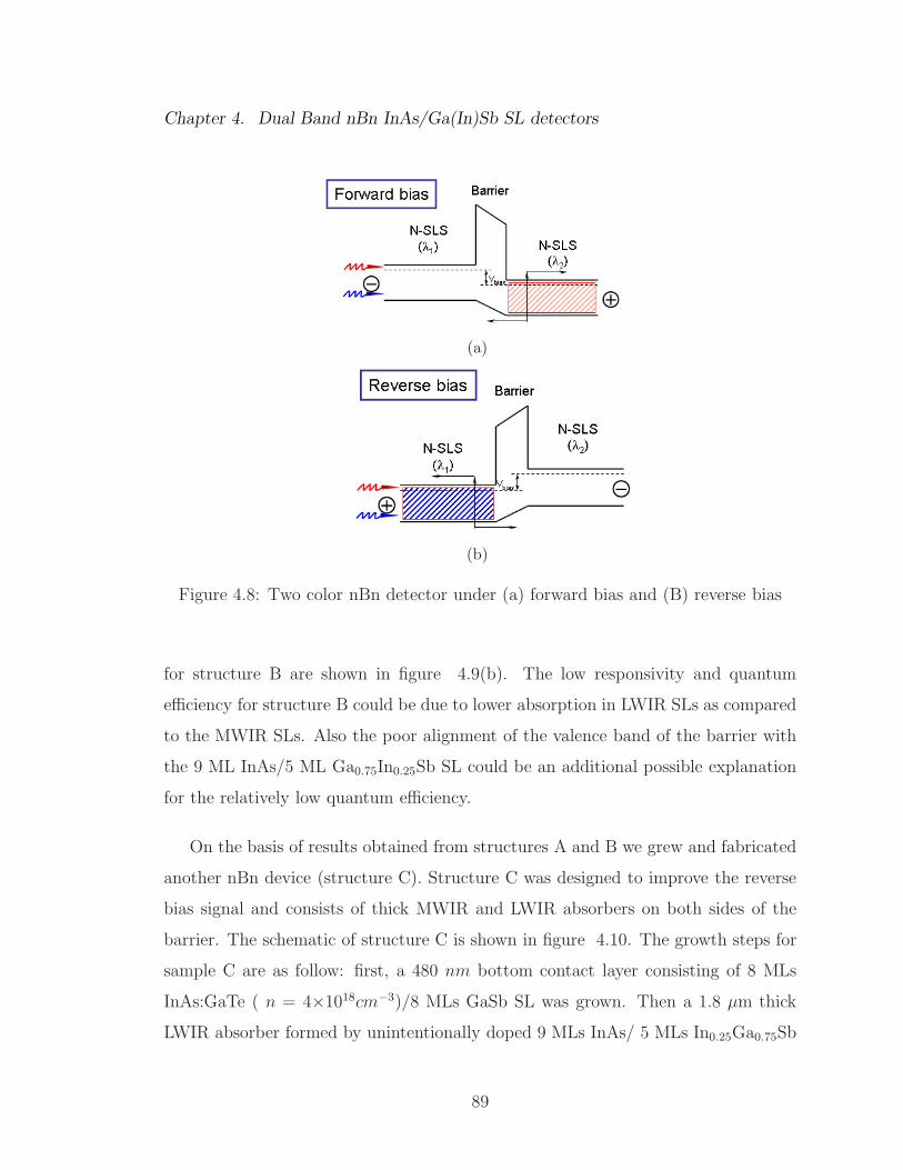
Chapter 4. Dual Band nBn InAs/Ga(In)Sb SL detectors
(a)
(b)
Figure 4.8: Two color nBn detector under (a) forward bias and (B) reverse bias
for structure B are shown in figure 4.9(b). The low responsivity and quantum
efficiency for structure B could be due to lower absorption in LWIR SLs as compared
to the MWIR SLs. Also the poor alignment of the valence band of the barrier with
the 9 ML InAs/5 ML Ga0.75In0.25Sb SL could be an additional possible explanation
for the relatively low quantum efficiency.
On the basis of results obtained from structures A and B we grew and fabricated
another nBn device (structure C). Structure C was designed to improve the reverse
bias signal and consists of thick MWIR and LWIR absorbers on both sides of the
barrier. The schematic of structure C is shown in figure 4.10. The growth steps for
sample C are as follow: first, a 480 nm bottom contact layer consisting of 8 MLs
InAs:GaTe ( n = 4×1018cm−3)/8 MLs GaSb SL was grown. Then a 1.8 µm thick
LWIR absorber formed by unintentionally doped 9 MLs InAs/ 5 MLs In0.25Ga0.75Sb
89
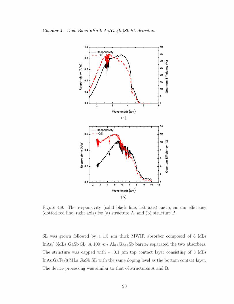
Chapter 4. Dual Band nBn InAs/Ga(In)Sb SL detectors
2 3 4 5 60.0
0.2
0.4
0.6
0.8
1.0
0
5
10
15
20
25
30
35
40
Res
pons
ivity
(A/W
)
Wavelength ( m)
Responsivity
Qua
ntum
Eff
icie
ncy
(%)
QE
(a)
2 3 4 5 6 7 8 9 10 110.0
0.2
0.4
0.6
0
2
4
6
8
10
12
14
Res
pons
ivity
(A/W
)
Wavelength ( m)
Responsivity
Qua
ntum
Eff
icie
ncy
(%)
QE
(b)
Figure 4.9: The responsivity (solid black line, left axis) and quantum efficiency(dotted red line, right axis) for (a) structure A, and (b) structure B.
SL was grown followed by a 1.5 µm thick MWIR absorber composed of 8 MLs
InAs/ 8MLs GaSb SL. A 100 nm Al0.2Ga0.8Sb barrier separated the two absorbers.
The structure was capped with ∼ 0.1 µm top contact layer consisting of 8 MLs
InAs:GaTe/8 MLs GaSb SL with the same doping level as the bottom contact layer.
The device processing was similar to that of structures A and B.
90

Chapter 4. Dual Band nBn InAs/Ga(In)Sb SL detectors
Figure 4.10: Structure C: Dual band MWIR/LWIR detector
As shown in figure 4.11, dark current density is higher in the forward bias regime
(1.25 A/cm2 at +0.5V ) as compared to the reverse bias (0.338 A/cm2 at -0.5 V ).
This is expected since the forward bias is dominated by the generation currents from
the LWIR absorber while the reverse bias is dominated by the generation currents
from the MWIR absorber. The dark current density in structure C is higher than
the current densities found for structures A and B which is due to the larger depth
of the first etch (∼1.5 µm) and therefore larger surface currents as compared to the
first etch depth for structures A and B(∼100 nm). The relatively large dark current
density in the three structures can be improved with the optimized composition and
thickness of the barrier layer.
The relative spectral responses for the bi-color structure is shown in figure 4.12.
The data clearly shows cutoff wavelengths λc1 ∼ 4.5 µm and λc2 ∼8 µm under
different polarities of applied bias. When forward bias is applied the carriers from
the LW absorber are collected and when the reverse bias is applied the carriers from
the MW absorber are collected.
91
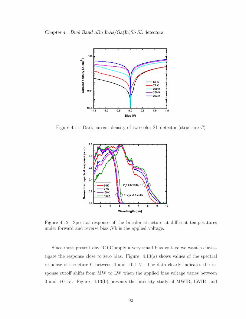
Chapter 4. Dual Band nBn InAs/Ga(In)Sb SL detectors
-1.5 -1.0 -0.5 0.0 0.5 1.0 1.51E-4
0.01
1
100
50 K 77 K 200 K 250 K 293 K
Cur
rent
den
sity
(A/c
m2 )
Bias (V)
Figure 4.11: Dark current density of two-color SL detector (structure C)
3 4 5 6 7 8 9 100.0
0.2
0.4
0.6
0.8
1.0
Vb= -0.6 volts
Vb= 0.5 volts
Nor
mal
ized
spe
ctra
l res
pons
e (a
.u.)
Wavelength ( m)
50K 77K100K 150K
Figure 4.12: Spectral response of the bi-color structure at different temperaturesunder forward and reverse bias ;Vb is the applied voltage.
Since most present day ROIC apply a very small bias voltage we want to inves-
tigate the response close to zero bias. Figure 4.13(a) shows values of the spectral
response of structure C between 0 and +0.1 V . The data clearly indicates the re-
sponse cutoff shifts from MW to LW when the applied bias voltage varies between
0 and +0.1V . Figure 4.13(b) presents the intensity study of MWIR, LWIR, and
92

Chapter 4. Dual Band nBn InAs/Ga(In)Sb SL detectors
MWIR to LWIR ratio vs applied bias voltage. As the applied bias voltage increases
from 0 to +0.1V , the MW intensity decreases, and LW intensity increases. The bias
dependent feature of the spectral response, can be exploited by post-processing algo-
rithms [45] to achieve high levels of spectral tuning and matched filtering. Due to this
feature, a single detector can be operated at multiple biases sequentially, whereby
the detector’s spectral response changes each time with the applied bias. Therefore,
the bias dependent spectral response can be used in algorithms to reconstruct the
sources in the surrounding environment.
4.6 Conclusion
The multi-spectral capabilities of SL-based nBn structures were demonstrated using
three different samples. Structure A and structure B showed two-color response
with the change of polarity of applied bias at 3.5/4.5µm, and 3.5/8µm, respectively.
Structure C was designed to have equal signal strengths from its absorbers under
different polarities of applied bias. The spectral response for structure C, showed
that LW to MW intensity ratio changes within very small bias voltage range which
results in less expensive and complex multi-color FPA technology.
93

Chapter 4. Dual Band nBn InAs/Ga(In)Sb SL detectors
2 3 4 5 6 7 8 9 10
Spec
tral
resp
onse
(a.u
)
Wavelength ( m)
0 V 0.01 V 0.05 V 0.09 V 0.1 V
T = 77K
(a)
0.00 0.02 0.04 0.06 0.08 0.100.00
0.01
0.02
0.03
0.04
0.05
0.06
0
2
4
6
8
10
12
14
16
Spec
tral
Res
pons
e(a.
u)
Applied Voltage(V)
3um
8um MW
IR/L
WIR
rat
io
3um/8um
(b)
Figure 4.13: (a)The spectral response of structure C between 0 and +0.1V bias volt-age, that is compatible with the bias range of present day ROICs. (b) the intensitystudy of MWIR, LWIR, and MWIR to LWIR ratio vs applied bias voltage at 77 K.
94
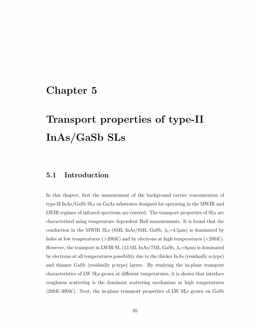
Chapter 5
Transport properties of type-II
InAs/GaSb SLs
5.1 Introduction
In this chapter, first the measurement of the background carrier concentration of
type-II InAs/GaSb SLs on GaAs substrates designed for operating in the MWIR and
LWIR regimes of infrared spectrum are covered. The transport properties of SLs are
characterized using temperature dependent Hall measurements. It is found that the
conduction in the MWIR SLs (8ML InAs/8ML GaSb, λc=4.5µm) is dominated by
holes at low temperatures (>200K) and by electrons at high temperatures (<200K).
However, the transport in LWIR SL (13 ML InAs/7ML GaSb, λc=8µm) is dominated
by electrons at all temperatures possibility due to the thicker InAs (residually n-type)
and thinner GaSb (residually p-type) layers. By studying the in-plane transport
characteristics of LW SLs grown at different temperatures, it is shown that interface
roughness scattering is the dominant scattering mechanism at high temperatures
(200K-300K). Next, the in-plane transport properties of LW SLs grown on GaSb
95

Chapter 5. Transport properties of type-II InAs/GaSb SLs
are studied. Due to highly conductive GaSb substrate, flip-chip bonding technique
was used to remove the substrate. The experimental data was then analyzed using
Quantitative Mobility Spectrum Analysis (QMSA) which showed indication of two
types of carriers in the LW SL material system with activation energies indicating
impurity donors.
5.2 Background and motivation
In order to further improve ambient temperature performance of detector material
in terms of issues such as collection efficiency, one needs to have a better under-
standing of underlying carrier transport in this material. The study of transport in
InAs/InGaSb SLs is important in its own right since carrier mobility affects charge
collection in both photoconductive and photovoltaic modes of operation.
However, electrical transport measurements on these structures are difficult, es-
pecially at high temperatures, as the SLs are grown on highly conductive GaSb
substrates. Commercially available GaSb substrates have, at best, a residual doping
level of low 1017cm−3 and substrates being significantly thicker than SLs, carriers
from the former will have an overbearing contribution to electrical transport.
Several techniques have been reported to measure and analyze the electrical prop-
erties by different groups [46, 47, 48, 49, 50]. Some groups have reported Hall mea-
surements by introducing a lattice matched quaternary AlGaAsSb buffer layer be-
tween the substrate and the superlattice [49], but this technique is only suitable at
low temperatures where quaternary layer conductivity is sufficiently low. Tempera-
ture dependent capacitance-voltage measurements on “p-i-n” SL-based diodes, have
been reported [51] and provide interesting values of background carrier concentration
between 20 and 200 K. However, capacitance-voltage measurements do not provide
complimentary information such as mobility and polarity of carriers.
96

Chapter 5. Transport properties of type-II InAs/GaSb SLs
In this study, we have grown both MW and LW SLs on GaAs substrates using
interfacial misfit dislocation (IMF) arrays [1]. GaAs substrate is used as it suppresses
the contribution of carriers from the substrate to the transport characteristics of SLs
as compared to highly conductive GaSb substrates. The dislocations associated with
large lattice mismatch between GaAs and GaSb are relieved at the GaAs/GaSb
interface by 90 degrees misfit dislocation using interfacial misfit dislocation arrays
(IMF) growth mode. We also have studied the in-plane transport properties of
LW SLs on GaSb, where the substrate has been removed by the flip-chip bonding
technique which the results are shown in the second part of the chapter.
5.3 Interfacial misfit dislocation arrays (IMF)
This method allows rapid strain relief at the heteroepitaxial interface through the
formation of a two dimensional (2D), periodic, IMF array comprised of pure edge,
90◦ dislocations along both [110] and [110] directions. The IMF growth mode results
in a high quality, thick GaSb epilayer on GaAs and exceptionally low defect densities
(<105cm−2).
5.3.1 Growth of the GaSb/GaAs using IMF method
The GaAs substrate is deoxidized at 600◦C prior to the growth of 100 nm of GaAs
at 560 ◦C to obtain a smooth surface. After completion of the homoepitaxy, the
substrate temperature is reduced to 510◦C under constant As overpressure. Before
the Sb growth is initiated, the As valve is closed allowing As adatoms to desorb
leaving a Ga-rich surface. This process, confirmed by RHEED transition from an
As-rich (2×4) to Ga-rich (4×2) surface, reduces As/Sb intermixing. Once the GaSb
growth begins, the RHEED pattern resembles a 1×3 indicating that a thin film of
97

Chapter 5. Transport properties of type-II InAs/GaSb SLs
GaSb forms on the surface.
Figure 5.1 shows the strain-relaxed low defect density GaSb (120 nm) buffer on
GaAs and the GaSb/GaAs interface along the [110] direction.
Figure 5.1: Cross-sectional TEM image of 120 nm of GaSb on GaAs showing a highlyperiodic array of misfit dislocations at the GaSb layer and the GaAs substrate [1].
5.4 Background carrier concentration of mid-wave
and long-wave superlattices grown on GaAs
It is interesting to note that the constituent materials of the SLs have different polar-
ity of background concentration. MBE grown InAs is residually n-type whereas GaSb
is residually p-type. Thus the background concentration in the SLs is expected to
depend on the thickness of the constituent InAs and GaSb layers. In this section, we
report on temperature dependent Hall measurements to extract the background car-
98

Chapter 5. Transport properties of type-II InAs/GaSb SLs
rier concentration and activation energies in 8ML InAs/8ML GaSb MWIR (λc ∼4.5
µm) and 13 ML InAs/7 ML GaSb LWIR (λc ∼8 µm) SLs grown on GaAs substrates.
The structures were grown on semi-insulating GaAs (100) substrates. After the
GaAs buffer layer, a layer of GaSb was grown using a layer of 90◦ interfacial misfit
(IMF) arrays to relieve the strain at the GaAs/GaSb interface [1]. This dramatically
reduces the number of threading dislocations that penetrate the active region of the
device. GaSb based lasers and solar cells have been realized with defect densities less
than 106cm−2[52, 53, 54]. In our structures, a non-intentionally doped 2µm thick SL
of 8 ML InAs/ 8 ML GaSb was grown for the MW sample, and a non-intentionally
doped 2µm thick SL of 13 ML InAs/7 ML GaSb was grown for the LW sample. A
0.45 ML thick InSb layer was used to compensate the strain between the InAs and
GaSb layers in the LW SLs. Detailed growth and interface optimization approaches
can be found in chapter 3. To study the effect of interface roughness on the transport
properties of LW SLs, four samples at different substrate temperatures were grown.
Magnetotransport measurements were performed on cleaved 1×1cm2 samples in
the van-der-Pauw configuration (using a Hall setup with high impedance buffers and
fully guarded voltage leads). AC excitation currents in the range of 100 to 500µA at
18 Hz were applied to obtain good signal to noise ratio for these highly conductive
samples. To control temperature in the range of 80 to 300 K, samples were mounted
inside a vacuum dewar on a Joule-Thomson refrigerator stage (MMR Technologies)
using silver paint (Fullam, Inc). Magnetic fields up to ±0.9 Tesla were applied normal
to the samples.
Figures 5.2(a),(b) and (c) show the resistivity, carrier concentration, and mobility
of the MW SL at different measurement temperatures, respectively. The bandgap
of the SLs is estimated to be 276 meV at 77 K and 248 meV at 300 K. The
temperature dependent resistivity of MW SL sample (Figure 5.2(a)) shows a distinct
change in the slope with temperatures below 200K showing an activation energy of
99
Chapter 5. Transport properties of type-II InAs/GaSb SLs
∼24 meV and temperatures above 200 K showing an activation energy of ∼193
meV . The discontinuous slope in this behavior indicates the presence of two types
of carriers, p-type carriers at low temperatures (< 200K) and n-type carriers at high
temperatures (> 200K) with very different activation energies. We believe that holes
arising out of shallow impurities close to the valence band edge with an activation
energy of ∼24 meV are the dominant source of conduction at T< 200K. At higher
temperatures (> 200K), the higher mobility electrons are activated from the deep
impurity level (193 meV ) and dominate the conduction. One possible source of these
deep levels is the shallow level impurities in bulk InAs layers which due to the band
line up between the InAs and SLs acts as deep impurity levels in the SL[15]. As
shown in figure 5.2(b), Hall measurements reveal a “p-type” material at T< 200K
and “n-type” material at higher temperatures. We believe that behavior is due to
the residual doping of the two constituent materials and their activation energies.
InAs is residually n doped and GaSb is residually p doped. At low temperatures,
holes in SL are activated due to their lower activation energy (23.86 meV ) than the
electrons and as the temperature increases the electrons from deep level impurities
(193 meV ) are activated and become the dominant source of conduction due to their
higher mobility. The measured mobility in the MW sample shown in figure 5.2(c)
also confirms the switching of majority carriers from holes to electrons at 200 K. As
is expected the holes (p-type carriers) have lower mobility than the electrons (n-type
carriers).
In-plane hall measurements were also performed on the LW SL samples which had
13 ML of InAs (residually n-doped) and 7 ML of GaSb, which is residually p-type
doped. A 0.45 ML of InSb was introduced to strain compensate the superlattice.
The bandgap of LW SL is estimated to be 150 meV at 77 K. This SL demonstrated
an n-type behavior across all measurement temperatures possibly due to the large
InAs thickness. Figure 5.3(a) shows the resistivity of the LW SL grown at 455 ◦C
as a function of measurement temperature. Activation energy extracted from the
100
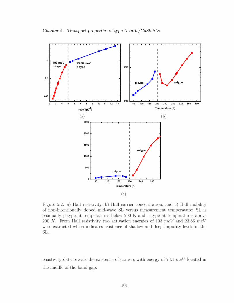
Chapter 5. Transport properties of type-II InAs/GaSb SLs
2 3 4 5 6 7 8 9 10 11 12 13
0.01
0.1
1
300 200Temperature (K)
193 meVn-type
R
esis
tivity
(cm
)
1000/T(K-1)
23.86 meVp-type
77
(a)
80 120 160 200 240 280 320 360 4001E16
1E17
p-type
Car
rier C
once
ntra
tion
(cm
-3)
Temperature (K)
n-type
(b)
80 120 160 200 240 2800
500
1000
1500
2000
2500
p-type
Mob
ility
(cm
2 /V.s
)
Temperature (K)
n-type
(c)
Figure 5.2: a) Hall resistivity, b) Hall carrier concentration, and c) Hall mobilityof non-intentionally doped mid-wave SL versus measurement temperature; SL isresidually p-type at temperatures below 200 K and n-type at temperatures above200 K. From Hall resistivity two activation energies of 193 meV and 23.86 meVwere extracted which indicates existence of shallow and deep impurity levels in theSL.
resistivity data reveals the existence of carriers with energy of 73.1 meV located in
the middle of the band gap.
101

Chapter 5. Transport properties of type-II InAs/GaSb SLs
It has been shown that the growth temperature has a significant effect on the
background concentration in LW SLs as shown by Burkle et al [49]. Figure 5.3(b)
shows the carrier concentration as a function of measurement temperature for the LW
SL samples grown at different temperatures. The carrier concentration is tempera-
ture independent in 80-125 K temperature range and as the temperature increases it
increases exponentially. We believe that the ionized vacancies and defects in the SL
are the source of carriers at low temperatures. As figure 5.3(c) shows, the samples
grown at higher temperature have larger carrier concentration at low measurement
temperatures which is due to larger vacancy and defect density, and the carrier
concentration is independent of growth temperatures for measurement temperatures
larger than 200 K. The thermally generated intrinsic carriers in the SL are the
dominant source of the carriers at these temperatures, therefore there is little carrier
concentration variation between samples grown at different substrate temperatures.
Theses carriers are intrinsic carriers associated with generation-recombination mech-
anism in the LW SL.
Figure 5.4(a) shows the mobility of the LW SL as a function of the measure-
ment temperature for the samples grown at different substrate temperatures. The
behavior follows the expected temperature dependence of mobility spectrum where
at low temperatures mobility is limited by ionized impurity scattering and at higher
temperatures mobility is phonon scattering limited. However, the dependence re-
lated to the ionized impurity and phonon scattering for SL do not exactly follow the
classical T3/2 and T−3/2 behavior for bulk material. This deviation is associated with
the SL material system in which interface scattering and defects are other sources
of scattering affecting the mobility. The effect of interface scattering is significant
when mobility spectra of the samples grown at different substrate temperatures are
compared. As shown in figure 5.4(a), for temperatures greater than 200 K, the
mobility of samples grown at higher substrate temperature is less dependent on the
measurement temperature. This behavior suggests that at higher growth tempera-
102

Chapter 5. Transport properties of type-II InAs/GaSb SLs
2 3 4 5 6 7 8 9 10 11 12 13 14
0.01
0.1
200 300 Temperature (K)
455 C sample
Res
istiv
ity (
cm)
1000/T(K-1)
73.1 meV
77
(a)
50 100 150 200 250 300
1E16
1E17
Car
rier c
once
ntra
tion
(cm
-3)
Temperature (K)
435 C 455 C 500 C 475 C
(b)
-100 -80 -60 -40 -20 01E15
1E16
1E17
140K 260K
Car
rier c
once
ntra
tion
(cm
-3)
Growth temperature- Tt (C)
Tt
(c)
Figure 5.3: a) Hall resistivity of non-intentionally doped long-wave SL versus mea-surement temperature, b) Hall carrier concentration versus measurement tempera-ture, and c) Hall carrier concentration dependence on growth temperature; SL isresidually n-type at all of the measurement temperatures. At low measurement tem-peratures extrinsic carriers and at high measurement temperatures intrinsic carriersare the dominant source of carriers in the LW SL.
tures interface scattering is the dominant source of the scattering as compared to
other sources of scattering like phonon and ionized impurity scattering, therefore SL
mobility is independent of the measurement temperature. Figure 5.4(b) shows the
103
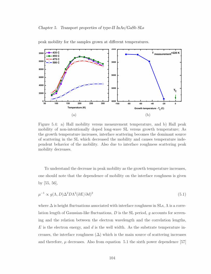
Chapter 5. Transport properties of type-II InAs/GaSb SLs
peak mobility for the samples grown at different temperatures.
50 100 150 200 250 3000
2000
4000
6000
8000
10000
12000
Mob
ility
(cm
2 /V.s
)
Temperature (K)
435 C 455 C 475 C 500 C
(a)
-100 -80 -60 -40 -20 04000
6000
8000
10000
12000
T measurement=220 K
Peak
mob
ility
(cm
2 /V.s
)Growth temperature - Tt (C)
Tt
(b)
Figure 5.4: a) Hall mobility versus measurement temperature, and b) Hall peakmobility of non-intentionally doped long-wave SL versus growth temperature; Asthe growth temperature increases, interface scattering becomes the dominant sourceof scattering in the SL which decreased the mobility and causes temperature inde-pendent behavior of the mobility. Also due to interface roughness scattering peakmobility decreases.
To understand the decrease in peak mobility as the growth temperature increases,
one should note that the dependence of mobility on the interface roughness is given
by [55, 56],
µ−1 ∝ g(Λ, D)∆2DΛ2(∂E/∂d)2 (5.1)
where ∆ is height fluctuations associated with interface roughness in SLs, Λ is a corre-
lation length of Gaussian-like fluctuations, D is the SL period, g accounts for screen-
ing and the relation between the electron wavelength and the correlation lengths,
E is the electron energy, and d is the well width. As the substrate temperature in-
creases, the interface roughness (∆) which is the main source of scattering increases
and therefore, µ decreases. Also from equation 5.1 the sixth power dependence [57]
104
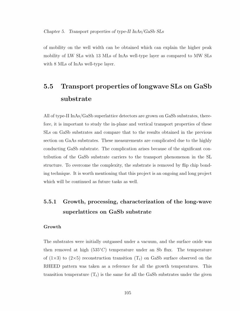
Chapter 5. Transport properties of type-II InAs/GaSb SLs
of mobility on the well width can be obtained which can explain the higher peak
mobility of LW SLs with 13 MLs of InAs well-type layer as compared to MW SLs
with 8 MLs of InAs well-type layer.
5.5 Transport properties of longwave SLs on GaSb
substrate
All of type-II InAs/GaSb superlattice detectors are grown on GaSb substrates, there-
fore, it is important to study the in-plane and vertical transport properties of these
SLs on GaSb substrates and compare that to the results obtained in the previous
section on GaAs substrates. These measurements are complicated due to the highly
conducting GaSb substrate. The complication arises because of the significant con-
tribution of the GaSb substrate carriers to the transport phenomenon in the SL
structure. To overcome the complexity, the substrate is removed by flip chip bond-
ing technique. It is worth mentioning that this project is an ongoing and long project
which will be continued as future tasks as well.
5.5.1 Growth, processing, characterization of the long-wave
superlattices on GaSb substrate
Growth
The substrates were initially outgassed under a vacuum, and the surface oxide was
then removed at high (535◦C) temperature under an Sb flux. The temperature
of (1×3) to (2×5) reconstruction transition (Tt) on GaSb surface observed on the
RHEED pattern was taken as a reference for all the growth temperatures. This
transition temperature (Tt) is the same for all the GaSb substrates under the given
105
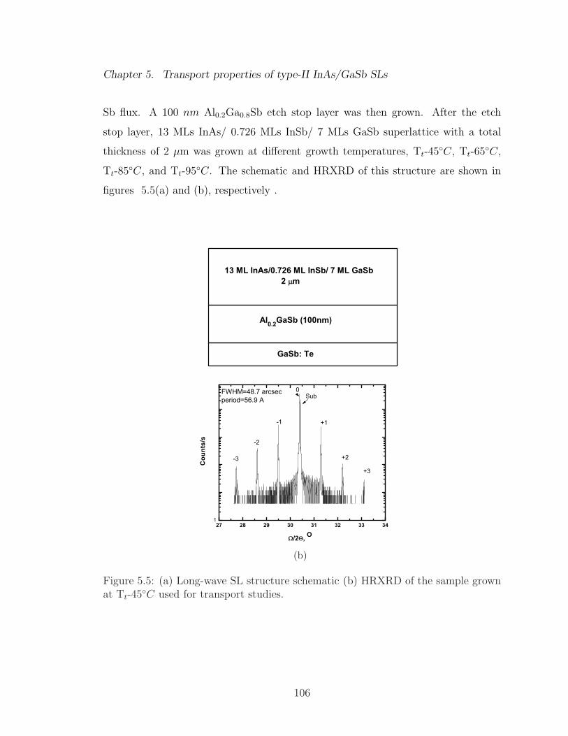
Chapter 5. Transport properties of type-II InAs/GaSb SLs
Sb flux. A 100 nm Al0.2Ga0.8Sb etch stop layer was then grown. After the etch
stop layer, 13 MLs InAs/ 0.726 MLs InSb/ 7 MLs GaSb superlattice with a total
thickness of 2 µm was grown at different growth temperatures, Tt-45◦C, Tt-65
◦C,
Tt-85◦C, and Tt-95
◦C. The schematic and HRXRD of this structure are shown in
figures 5.5(a) and (b), respectively .
GaSb: Te
Al0.2GaSb (100nm)
13 ML InAs/0.726 ML InSb/ 7 ML GaSb 2 m
27 28 29 30 31 32 33 341
-3
-2
+3
+2
/2 , O
Cou
nts/s
FWHM=48.7 arcsecperiod=56.9 A
+1-1
Sub0
(b)
Figure 5.5: (a) Long-wave SL structure schematic (b) HRXRD of the sample grownat Tt-45
◦C used for transport studies.
106
Chapter 5. Transport properties of type-II InAs/GaSb SLs
Processing
Three masks were used in this step. SiN was deposited at the top of the sample.
Standard optical photolithography was used for all the three steps. In the first step
the sample was etched to the top of the SLs. Then UBM was deposited as Ti/Ni/Au
(50/50/400 nm). In the last step a 1.5 µm thick indium layer was deposited. Also,
processing of fanout included deposition of metal contacts Ti/Ni/Au (50/50/400
nm). Next, Reflow and bonding of the sample and fanout were done, and then the
substrate was removed. The schematic of the main steps of processing are shown in
figure 5.6.
(a) ICP
SiN
(a) ICP
(b) UBM (Ti/Pt/Au/Ni)
(b) UBM(Ti/Pt/Au/)Ni(c) Indium deposition
(c) ICP
(d) Reflow
(d) UBM(Ti/Pt/Au/)Ni(e)Metal contact
(e) ICP
(f) Flip-chip bonded
(f) UBM(Ti/Pt/Au/)Ni(g) Substrate removed
(g) ICP
Figure 5.6: Main steps of processing for substrate removal (flip-chip method)
107

Chapter 5. Transport properties of type-II InAs/GaSb SLs
Characterization
To study the lateral and vertical SL transport, different sample geometries are used.
In this section the lateral transport geometry and measurements are presented. The
vertical transport studies are an ongoing project and will be mentioned as future work
in chapter 6. To study the lateral transport, the processed flip-chip samples are used
in the van der Pauw configuration (figure 5.7). In the van der Pauw measurements
four ohmic contacts are placed on the sample, where the contacts must be on the
boundary of the sample and must be very small (see figure 5.7).
Figure 5.7: Classical form of the sample for van der Pauw method measurements.
1
3
4
InAs/InSb/GaSb SLs
2
Ti/Ni/Au Contacts
Figure 5.8: The van der Pauw configuration for lateral LW SL transport studies
To make a measurement, current passes along one edge (3,4) of the sample and
the voltage across the opposite edge (1,2) is measured. From these two values, a
108

Chapter 5. Transport properties of type-II InAs/GaSb SLs
resistance is found:
R1234 =V12
I34(5.2)
Hall coefficient and resistivity are obtained as following:
RH =W
BR1234 (5.3)
Where RH is the hall coefficient, B is the magnetic field and W is the sample thick-
ness.
ρ =πW
ln2
(
R1234 +R2341
2
)
f(Q) (5.4)
Where ρ is the resistivity and f(Q) is a factor which is only a function of ratio
R1234/R2341. R1234/R2341 and f(Q) are related through the following transcendental
equation,
cosh
{
(R1234/R2341)− 1
(R1234/R2341) + 1
ln 2
f
}
=1
2exp
ln 2
f(5.5)
The hall experimental data is analyzed by Quantitative Mobility Spectrum Analy-
sis (QMSA) method. QMSA is a method and apparatus to produce the conductivity-
mobility spectrum of an isotropic semiconductor material using the experimental
data this algorithm gives the electrical transport information under high magnetic
fields on multiple carrier devices.
As shown in figure 5.9(a), hall coefficient and resistivity were measured for
magnetic fields up to 12 T . figure 5.9(b) shows the mobility spectrum obtained
from QMSA analysis of data shown in figure 5.9(a). QMSA shows indication of
two carriers shown as E1 and E2 in figure 5.9(b). All of the peaks under E2 are
considered as one carrier (E2). As shown in figure 5.9(c) the fit shows a broad
spectrum (E2) for wide range of temperatures which could be related to the errors
associated with the QMSA algorithm. In figure 5.9(b), holes from this spectrum
109

Chapter 5. Transport properties of type-II InAs/GaSb SLs
were interpreted as ghost peaks. These are an artifact from the QMSA algorithm,
caused essentially by noise. The algorithm adds holes under the electron peak in
order to obtain the best fit to the experimental data.
Carrier concentration of the two types of the carriers was calculated using :
n =σ
eµ(5.6)
Where σ is the conductivity and µ is the mobility obtained from QMSA. The carrier
concentration vs 1000/T is curve fit to the equation:
n =n0,s
We−
Ea
KBT
(5.7)
Where EA (the activation energy) , and n0,s (density of states) are found to be 10.8
meV , 6.1×1013cm−2 for E1 and 7.29 meV , 1.9×1013cm−2 for E2 ( figure 5.10(a)).
The activation energies indicates shallow impurity donors of about 10 meV below
the conduction band of the SL, which is shown as the dashed line in figure 5.10(b).
5.6 Conclusion
The residual doping of the 8 ML InAs/ 8 ML GaSb on GaSb substrate is found
to change from p type to n type as the measurement temperature increases. The
transition was attributed to the difference in activation energies of p-type and n-type
carriers in the MW SL. In-plane transport study on 13 ML InAs/0.45 ML InSb/ 7
ML GaSb (LW samples) shows n-type carriers for all the measured temperatures.
By varying the substrate temperature during the growth, it is found that interface
scattering is one of the dominant sources of the carrier scattering mechanisms in the
SL material system, and affects the transport properties of the SL. Also, transport
measurement of SLs grown on GaSb were analyzed by quantitative mobility spectrum
110

Chapter 5. Transport properties of type-II InAs/GaSb SLs
analysis algorithm. Two types of carriers (E1 and E2) were extracted with mobilities
in high 102cm2/V.s and low 104cm2/V.s for E1 and E2, respectively. Activation
energies of E1 and E2 indicate shallow impurity level donors close to the conduction
band of the SL.
Due to different errors associated with the sample geometry, hall measurements,
and QMSA algorithm, another set of samples will be studied for both in-plane and
vertical SL transport studies on GaSb substrates.
111

Chapter 5. Transport properties of type-II InAs/GaSb SLs
0 2 4 6 8 10 12
-50
-40
-30
-20
-10
0
0.005
0.010
0.015
0.020
0.025
0.030
0.035
0.040
Res
istiv
ity,
(cm
)
RH
Hal
l Coe
ffici
ent (
cm3 /C
)
Magnetic Field, B (T)
(a)
102 103 104 105 106
0
5
10
15
E2
Con
duct
ivity
(cm
-1)
Mobility (cm2/Vs)
Electrons Holes
Mobility Spectrum at 77K
E1
(b)
0
5
10
15
20
25
102 103 104 105 106
290
167
77
45
E2
32K 45K 77K 167K 290K
E1
32
T
cm-1
( cm2/Vs)
(c)
Figure 5.9: (a) Hall experimental data for magnetic field rang of 0-12 T (b) Mobilityspectra obtained from QMSA algorithm at 77 K (c) Mobility spectra obtained fromQMSA algorithm at temperature range of 32-290 K.
112

Chapter 5. Transport properties of type-II InAs/GaSb SLs
5 10 15 20 25 30
1E16
1E17
n0,s
= 1.9 x 1013 cm-2
C
once
ntra
tion
(cm
-3)
1000/T (K-1)
E1 E2EA=10.8 meV
n0,s
= 6.1 x 1013 cm-2
EA=7.29 meV
(a)
(b)
Figure 5.10: (a) Carrier concentration versus 1/T for LWIR SLs on GaSb substrate;Two activation energies are extracted, indicating (b) shallow impurity donor levelsclose to the SL conduction band
113

Chapter 6
Conclusions and Future Work
6.1 Conclusion
This work is focused on development of high performance infrared InAs/GaSb SL
detectors. SL detector technology has inherent advantages over present-day detec-
tion technologies. InAs/GaSb SL has high responsivity because of strong absorption
of normal incidence photons. Larger electron effective masses that are not directly
dependent on the bandgap energy lower the tunneling current compared with bulk
materials with the same bandgap energy. Different combinations of superlattice pe-
riodicity or constituent material composition can be utilized to tune the superlattice
bandgap which can be used to provide multicolor capability. Also, the light-hole and
heavy-hole band separation can be adjusted to reduce Auger recombination.
In chapter 1 of this dissertation we introduced the general concept of infrared
detection. Detection principles (with concentration on photovoltaic effect), detector
types (thermal and photon) and conventional figures of merit (external quantum
efficiency, noise equivalent power, spectral detectivity) were discussed. Finally, pros
and cons of competitive infrared technologies (MCTs, bulk InSb, and QWIPs) were
114

Chapter 6. Conclusions and Future Work
described and alternative technology for IR detection (based on type-II InAs/GaSb
SLs) was introduced.
In chapter 2 the design, growth, processing, optical and electrical characteriza-
tion of InAs/GaSb IR detectors were explained. We used next-nano and sentaures
TCAD softwares for the simulation of the SLs. Material growth using solid source
molecular beam epitaxy was briefly explained. We characterized structural, optical
and morphological properties of as-grown material by XRD, absorption and AFM
techniques, respectively. Processing of a single-pixel device was also covered. The
optical and electrical characterization of the devices included the explanation of tem-
perature dependent IV measurements, spectral response measurements using a FTIR
spectrometer and the responsivity measurement setup.
In chapter 3, first the growth of InAs/GaSB SLs on GaSb substrates by molec-
ular beam epitaxy (MBE) technique was presented. The two main parameters of
temperature and interfaces for the growth of SLs were discussed. We found that op-
timal temperature for deposition of SL is 45◦ lower than temperature Tt of (1×3) to
(2×5) reconstruction transition observed on the GaSb surface under 1×10⁶ Sb-flux.
Choice of shutter sequence during SL growth is important since it determines which
type of interface (“GaAs” - like, “InSb-like”, or both) will be formed between compo-
sitionally abrupt GaSb and InAs layers. We found introducing InSb layer for strain
compensation between InAs and GaSb layers produces the best structural proper-
ties. Since the lattice constant of InSb (GaAs) is much larger (smaller) than that of
the GaSb, an insertion of few monolayers of these materials into SL allows to grow
strain-compensated SL material. Thus, detectors with thick SL region (absorber)
can be grown without degrading its quality. Since external quantum efficiency is
proportional to the absorber thickness, detectors with enhanced values of QE can be
grown. Detector strucutre with 2 µm of SL absorbing region has been grown. The
HRXRD analysis revealed excellent crystalline quality of the film; the FWHM of the
115
Chapter 6. Conclusions and Future Work
first order satellite SL peak was found to be equal to 16 arcsec and lattice mismatch
was about 0%. In this chapter, high performance mid-infared pin InAs/GaSb SL
detector (λcut−off was ∼ 4.5 µm at 77 K ) grown by molecular beam epitaxy was
presented. The structural, optical and electrical properties were characterized using
X-ray crystallography, IV and responsivity measurements. At Vb = -0.3 V , the total
dark current was equal to 1.34×10⁻⁶ at 77 K which is comparable to the lowest
published dark current densities reported by other groups.
Next, based on the optimized longwave growth conditions, three long-wave pin
devices with different absorbing region doping were studied. The long-wave pin
with 5E15 cm-3 absorber p-doping level showed the best device performance. The
concept of nBn devices was presented. Devices based on nBn design have lower dark
current density as compared to the conventional pin designs due to suppression of
the currents associated with Shockley-Read-Hall centers and mesa lateral surface
imperfections. The comparison between shallow etched long-wave nBn device and
the optimized long wave pin device (5E15 cm-3 p-doped absorbing region) showed
nBn devices have the potential to have higher signal to noise ration as compared
to the pin devices. Temperature dependent I-V measurements showed 0.05 A/cm2
dark current density at + 0.1 V for nBn device as compared to 0.2 A/cm2 at -0.1 V
at 77 K for pin device. Also nBn devices showed higher responsivity as compared
to the pin devices due to elimination of Shockley-Reed-Hall recombination centers
associated with depletion regions and therefore, more carriers are extracted from the
absorbing region which increases the responsivity of these devices. nBn devices can
be further optimized by studying the barrier and absorber doping level as well as
barrier material and composition.
In chapter 4 the growth, processing and characterization of two-color InAs/GaSb
SL nBn detectors with cutoff wavelengths in mid-wave and long-wave regimes were
presented. First, growth, processing and characterization of the two samples, re-
116

Chapter 6. Conclusions and Future Work
ferred to structures A and B were presented. Both structures A and B had identical
structure except structure A had a midwave absorbing region and structure B had a
long-wave absorbing region. Two structures were fabricated out of the same growth
material, one with a shallow top contact isolation etch and one with a conventional
mesa structure for both mid-wave (A), and long-wave (B) samples. The shallow
etched device dark current was reduced by two orders of magnitude at 77 K com-
pared with the deep etched device for structure A. The current density was equal
to 2.3×10⁻⁶A/cm2 and 3.1×10⁻⁴A/cm2 for shallow and deep etched devices at Vb
= 0.1 V and T = 77 K, respectively. The responsivity and QE for sample A were
measured at 4 µm to be 0.74 A/W and 23% respectively.The responsivity for sample
B was low, 0.51 A/W at 5.5 µm, the expectation is that this will be increased in
future devices.
Spectral response showed that the two color responses ( λc1 ∼3.5 µm and λc2 ∼4.5
µm) and( λc1 ∼3.5 µm and λc2 ∼8.0 µm ) at 100 K and 150 K for samples A and
B , respectively, under different polarity of applied bias. Under forward bias the
photocarriers from the absorber are collected. Absorber layers are SL 8×8 MLs
InAs/GaSb (λc2 ∼ 4.5 µm) and SL 9×5 MLs InAs/In0.25Ga0.75Sb (λc2 ∼ 8.0 µm)
for structures A and B, respectively. When the device is under reverse bias the
photocarriers from the heavily n-doped top contact layer (SL InAs/GaSb 8x8 MLs)
are collected and the photocarriers from the absorber are blocked by the barrier.
Heavily doped InAs in 0.0972 µm InAs/GaSb SL of the top contact layer, results in
a larger optical bandgap due to the Moss-Burstein effect and is the source of the signal
at the shorter wavelength for both of the structures A and B. It is also important
to mention that reverse bias signal is (50-100 times) weaker than the forward bias
signal, which is consistent with the fact that the top contact layer is thinner and
heavily doped in comparison with the absorber.
On the basis of results obtained from structures A and B another dual-color nBn
117
Chapter 6. Conclusions and Future Work
device (structure C) was grown and fabricated. Structure C was designed to improve
the reverse bias signal and consists of thick MWIR and LWIR absorbers on both sides
of the barrier. It consisted equal thickness of both MWIR and LWIR absorber regions
separated with Al0.2GaSb barrier. The spectral response showed cutoff wavelengths
λc1 ∼4.5 µm and λc2 ∼8.0 µm under different polarities of applied bias. When
forward bias is applied the carriers from the LW absorber are collected and when the
reverse bias is applied the carriers from the MW absorber are collected. The spectral
response for structure C, showed that LW to MW intensity ratio changes within very
small bias voltage range which results in less expensive and complex multi-color FPA
technology.
Chapter 5 was devoted to transport studies of both mid-wave and lon-wave
InAs/GaSb SL material system. To prevent the effect of carriers from the high
conducting GaSb substrates, two methods were undertaken. In the first method,
samples were grown on semi-insulating GaAs substrates. In the second method the
GaSb substrate was removed by flip chip bonding technique.
The residual doping of the 8 ML InAs/ 8 ML GaSb grown on GaAs was found
to change from p-type to n-type as the measurement temperature was increased.
The transition was attributed to the difference in activation energies of p-type and
n-type carriers in the MW SL. In-plane transport study on 13 ML InAs/0.45 ML
InSb/7 ML GaSb (LW samples) grown on GaAs showed n-type carriers for all the
measured temperatures. By varying the substrate temperature during the growth,
it was found that interface scattering is one of the dominant sources of the carrier
scattering mechanisms in the SL material system, and affects the transport properties
of the SL. Also, transport measurement of LW SLs grown on GaSb were analyzed by
quantitative mobility spectrum analysis algorithm. Two types of carriers (E1 and
E2) were extracted with mobilities in high 102cm2/V.s and low 104cm2/V.s for E1
and E2, respectively. Activation energies of E1 and E2 indicate shallow impurity
118

Chapter 6. Conclusions and Future Work
level donors close to the conduction band of the SL. Further investigation of lateral
and vertical transport properties of SLs will be covered as future work plan.
6.2 Future work
6.2.1 SL transport studies
One of the fundamental properties of the SLs absorber layer is the background carrier
concentration as it determines the minority carrier lifetime and diffusion lengths of
carriers. As it was described in chapter 5, in order to study the transport properties
of SLs grown on GaSb substrates, one needs to avoid the highly conducting GaSb
substrate carriers. Therefore, different techniques are used to remove the substrate.
In order to remove the GaSb substrate, two different techniques will be used.
The first method is the flip-chip bonding technique that was covered in chapter 5
for lateral transport studies. However, our previous measurements were erroneous
due to the sample geometry, hall measurements, and QMSA algorithm. As a result,
these measurements will be repeated with the flip-chip bonding substrate removal
technique.
Another method to remove the substrate is to use mechanical and chemical pol-
ishing techniques. Figure 6.1 shows a set of processing steps [50] for removing the
SL substrate in lateral transport studies. In this method, InAsSb etch stop layer is
grown between the buffer layer and SL epi-layer. The sample is frontside-bonded to
a host substrate using liquid epoxy adhesive. After mechanical polishing of GaSb
substrate down to 80/100 µm thickness,selective wet etchants can be used to remove
the GaSb substrate as well as the InAsSb etch stop layer.
To study the vertical transport properties a different sample geometry is used.
119

Chapter 6. Conclusions and Future Work
Figure 6.1: Mechanical and chemical processing steps for GaSb substrate removal
In this geometry, the conduction of the GaSb substrate does not contribute to the
transport study, therefore substrate is not removed. Figure 6.2 shows the possible
sample geometry to study the vertical transport in the SLs.
Current
Metal Contact
InAs/GaSbSuperlattice
L
Mesa Seperation GaSb Substrate
Figure 6.2: SL sample geometry for vertical transport study
For the vertical transport sample geometry, pixels are defined by mesa isolation
etch where voltage is applied between the tops of the mesas and current is measured
as a function of magnetic field. Due to this geometry, the current flow direction
measured in this method is perpendicular to the current flow direction in the sub-
strate, therefore the transport properties of the GaSb substrate does not affect the
120

Chapter 6. Conclusions and Future Work
measurement results.
6.2.2 Minority carrier lifetime
To date, there is no comprehensive study correlating the carrier lifetime to the struc-
tural properties, and growth parameters of the SL. Such a systematic study will
provide invaluable data such as the minority carrier diffusion length and lifetime
and intersubband relaxation time that will enable to determine the limiting scat-
tering mechanisms in InAs/GaSb system, such as Shockley Read Hall and Auger
recombination.
6.2.3 Device performance optimization for pin and nBn de-
tectors
In order to improve the surface leakage currents in longwave pin detectors, a stable
passivant is required to prevent the oxidation of GaSb layers in the SL material
system.
Also, for improving the device performance of the long-wave nBn detectors and
to prevent the dark currents associated with SRH centers, an optimized barrier with
zero valence band off set is required. This requires a comprehensive study of band
alignment of different material system with the SL band alignment.
6.2.4 Alternative designs
• Type-II InAs/GaSb SLs grown on GaSb substrates, still suffers from a relatively
high cost mainly associated with its substrate. GaSb substrates are expensive
and are limited to 2” diameter or smaller wafers. For this reason, there is
121

Chapter 6. Conclusions and Future Work
a great deal of interest in SL on GaAs/Si substrates, which are cheaper and
are available in larger wafer sizes, both of which reduce the manufacturing
costs. In order to grow SLs on alternative substrates a detailed study of effect
of different interfaces, and growth optimization techniques on structural and
optical properties of SL detectors is required.
• InAsSb based infrared detectors are important for non-cryogenic thermal imag-
ing applications in the mid wave infrared (MWIR). InAsSb material system can
provide cheap, robust and inexpensive infrared detectors as they are based on a
mature III-V compound semiconductor technology. Lattice matched InAsSb on
GaSb substrate ( 9% Sb) show excellent material quality for midwave infrared
(MWIR) regime. IR detectors using nBn design have also shown promising
results in eliminating the currents associated with Shockley-Read-Hall centers
and mesa lateral surface imperfections that increases the operating temper-
ature. The goal is to produce room temperature mid-wave InAsSb infrared
detectors based on nBn design. The study requires detailed study of barrier in
terms of material, composition and doping level.
6.2.5 Design of very longwave infrared (VLWIR) detector
and theoretical modeling
Very long wavelength infrared (VLWIR) applications, such as space-based astron-
omy and remote pollution monitoring, require detectors with high performance and
stability over broad temperature ranges. In order to use InAs/GaSb SLs for VLWIR
regime, different InAs and GaSb layer thicknesses and different strain compensating
interface layers need to be investigated. Initial work on modeling an InSb strain
compensating layer and structural optimization has been performed, however the
effect of this strain compensating layer and optimization of InAs/InSb/GaSb layers
122
Chapter 6. Conclusions and Future Work
on the device performance need to be investigated. Figure 6.3(a) and (b) show next
nano simulations for 16 MLs of InAs/0.856 MLs of InSb/ 7 MLs of GaSb band align-
ment and dispersion diagram, respectively. Figure 6.3(c) shows the best structural
properties in terms of lattice mismatch and FWHM of first order SL peak which is
achieved by 0.86 MLs of strain compensating InSb layer grown between InAs and
GaSb layers.
123

Chapter 6. Conclusions and Future Work
0 2 4 6
-0.6
-0.4
-0.2
0.0
0.2
0.4
0.6
0.8
1.0
Ene
rgy
(eV
)
Distance (nm)
Conduction Heavy hole Light hole
6 ML GaSb0.856 ML InSb
16 ML InAs
0 K
(a)
0.0 0.2 0.4 0.6 0.8 1.0
-0.4
-0.3
-0.2
-0.1
0.0
0.1
Ene
rgy
(eV
)
Kz(x /L)
Conduction Band Heavy Hole Band Light Hole Band
0 K
(b)
0.72 0.78 0.84 0.90 0.96 1.02 1.080
10
20
30
40
0.00
0.02
0.04
0.06
0.08
0.10
0.12
FWH
M o
f 1st
ord
er S
L pe
ak (a
rcse
c)
InSb thickness, ML
a/a|, %
(c)
Figure 6.3: (a) next-nano band alignment simulation of 16 MLs InAs/0.86 MLsInSb/7 MLs GaSb (b) next-nano dispersion diagram which indicates a cut-off wave-length of 12 µm at 0 K (c) Growth optimization for VLWIR SL structure using InSbstrain compensating layer
124
References
[1] S. H. Huang, G. Balakrishnan, M. Mehta, A. Khoshakhlagh, L. R. Dawson,D. L. Huffaker, and P. Li, “Epitaxial growth and formation of interfacial misfitarray for tensile gaas on gasb,” Applied Physics Letters, vol. 90, no. 16, p.161902, 2007. [Online]. Available: http://link.aip.org/link/?APL/90/161902/1
[2] A. Rogalski and P. Martyniuk, “Inas/gainsb superlattices as a promis-ing material system for third generation infrared detectors,” Infrared
Physics & Technology, vol. 48, no. 1, pp. 39 – 52, 2006. [Online].Available: http://www.sciencedirect.com/science/article/B6TJ9-4G9935K-8/2/d7c6f7136b0a76c990a432e0362887e4
[3] M. Tidrow, W. Beck, W. Clark, H. Pollehn, J. Little, N. Dhar,R. Leavitt, S. Kennerly, D. Beekman, A. Goldberg, and Others, “Devicephysics and focal plane array applications of QWIP and MCT,” Opto-
Electronics Review, vol. 7, no. 4, pp. 283–296, 1999. [Online]. Available:http://www.inh.wat.edu.pl/review/optor/1999/4/7(4)283.pdf
[4] C. Hansson, “Comparative study of infrared photodetectors based on quantumwells (qwips) and quantum dots (qdips),” Master’s thesis, Halmstad University,2006.
[5] I. Vurgaftman, J. R. Meyer, and L. R. Ram-Mohan, “Band parametersfor iii–v compound semiconductors and their alloys,” Journal of Applied
Physics, vol. 89, no. 11, pp. 5815–5875, 2001. [Online]. Available:http://link.aip.org/link/?JAP/89/5815/1
[6] M. Razeghi, “Overview of antimonide based iii-v semiconductor epitaxial layersand their applications at the center for quantum devices,” THE EUROPEAN
PHYSICAL JOURNAL APPLIED PHYSICS, vol. 23, pp. 149–205, 2003.
125

References
[7] L. Esaki, “A bird’s-eye view on the evolution of semiconductor superlatticesand quantum wells,” Quantum Electronics, IEEE Journal of, vol. 22, no. 9, pp.1611–1624, Sep 1986.
[8] M. R. Kitchin and M. Jaros, “Characterization of gasb/inas typeii infrared detectors at very long wavelengths: carrier scatter-ing at defect clusters,” Physica E: Low-dimensional Systems and
Nanostructures, vol. 18, no. 4, pp. 498 – 508, 2003. [Online].Available: http://www.sciencedirect.com/science/article/B6VMT-4876CYY-2/2/399e932f72c8c28cb17376400153088b
[9] G. C. Dente and M. L. Tilton, “Pseudopotential methods for superlattices:Applications to mid-infrared semiconductor lasers,” Journal of Applied
Physics, vol. 86, no. 3, pp. 1420–1429, 1999. [Online]. Available:http://link.aip.org/link/?JAP/86/1420/1
[10] P.-Y. Delaunay, B. M. Nguyen, D. Hoffman, and M. Razeghi, Quantum Elec-
tronics, IEEE Journal of, vol. 44, no. 5, pp. 462–467, May 2008.
[11] D. Z.-Y. Ting, C. J. Hill, A. Soibel, S. A. Keo, J. M. Mumolo, J. Nguyen,and S. D. Gunapala, “A high-performance long wavelength superlattice com-plementary barrier infrared detector,” Applied Physics Letters, vol. 95, no. 2, p.023508, 2009. [Online]. Available: http://link.aip.org/link/?APL/95/023508/1
[12] B.-M. Nguyen, S. Bogdanov, S. A. Pour, and M. Razeghi, “Minority electronunipolar photodetectors based on type ii inas/gasb/alsb superlattices for verylong wavelength infrared detection,” Applied Physics Letters, vol. 95, no. 18, p.183502, 2009. [Online]. Available: http://link.aip.org/link/?APL/95/183502/1
[13] Y. Wei, A. Hood, H. Yau, A. Gin, M. Razeghi, M. Z. Tidrow, and V. Nathan,“Uncooled operation of type-ii inas/gasb superlattice photodiodes in themidwavelength infrared range,” Applied Physics Letters, vol. 86, no. 23, p.233106, 2005. [Online]. Available: http://link.aip.org/link/?APL/86/233106/1
[14] Y. Wei, A. Hood, H. Yau, V. Yazdanpanah, M. Razeghi, M. Z. Tidrow, andV. Nathan, “High-performance type-ii inas/gasb superlattice photodiodes withcutoff wavelength around 7 mu m,” Applied Physics Letters, vol. 86, no. 9, p.091109, 2005. [Online]. Available: http://link.aip.org/link/?APL/86/091109/1
[15] G. J. Sullivan, A. Ikhlassi, J. Bergman, R. E. DeWames, J. R. Waldrop,C. Grein, M. Flatte, K. Mahalingam, H. Yang, M. Zhong, and M. Weimer,“Molecular beam epitaxy growth of high quantum efficiency inas/gasbsuperlattice detectors,” vol. 23, no. 3, pp. 1144–1148, 2005. [Online]. Available:http://link.aip.org/link/?JVB/23/1144/1
126

References
[16] B.-M. Nguyen, D. Hoffman, P.-Y. Delaunay, and M. Razeghi, “Dark currentsuppression in type ii inas/gasb superlattice long wavelength infrared photo-diodes with m-structure barrier,” Applied Physics Letters, vol. 91, no. 16, p.163511, 2007. [Online]. Available: http://link.aip.org/link/?APL/91/163511/1
[17] A. Khoshakhlagh, J. B. Rodriguez, E. Plis, G. D. Bishop, Y. D. Sharma,H. S. Kim, L. R. Dawson, and S. Krishna, “Bias dependent dual bandresponse from inas/ga(in)sb type ii strain layer superlattice detectors,”Applied Physics Letters, vol. 91, no. 26, p. 263504, 2007. [Online]. Available:http://link.aip.org/link/?APL/91/263504/1
[18] E. H. Aifer, J. G. Tischler, J. H. Warner, I. Vurgaftman, J. R. Meyer,C. L. Canedy, and E. M. Jackson, “Dual band lwir/vlwir type-ii superlatticephotodiodes,” Infrared Technology and Applications XXXI, vol. 5783, no. 1, pp.112–122, 2005. [Online]. Available: http://link.aip.org/link/?PSI/5783/112/1
[19] W. Harrison, Electronic Structure and the Properties of Solids, reprint ed. DoverPublications, 1980.
[20] C. Kitte, Quantum Theory of Solids, second revised printining ed. New York:Wiley, 1987.
[21] P. .Yu and M. Cardona, Fundamentals of Semiconductors: Physics and Mate-
rials Properties, 3rd ed. Springer, 2005.
[22] [Online]. Available: http://www.nextnano.de/nextnano3/
[23] J. Steinshnider, M. Weimer, R. Kaspi, and G. W. Turner, “Visualizing interfacialstructure at non-common-atom heterojunctions with cross-sectional scanningtunneling microscopy,” Phys. Rev. Lett., vol. 85, no. 14, pp. 2953–2956, Oct2000.
[24] P. M. Thibado, B. R. Bennett, M. E. Twigg, B. V. Shanabrook, and L. J.Whitman, “Origins of interfacial disorder in GaSb/InAs superlattices,” Applied
Physics Letters, vol. 67, no. 24, pp. 3578–3580, 1995. [Online]. Available:http://link.aip.org/link/?APL/67/3578/1
[25] G. G. P. . F. I. Blefeld, R.; Osbourn, “The preparation and characterizationof strained-layer superlattices in the gaas+ gap system,” Journal of Electronic
Materials, vol. 12, pp. 903–915, 1983.
[26] J. W. Little, S. P. Svensson, W. A. Beck, A. C. Goldberg, S. W.Kennerly, T. Hongsmatip, M. Winn, and P. Uppal, “Thin active region,type II superlattice photodiode arrays: Single-pixel and focal plane array
127
References
characterization,” Journal of Applied Physics, vol. 101, no. 4, p. 044514, 2007.[Online]. Available: http://link.aip.org/link/?JAP/101/044514/1
[27] R. Kaspi, C. Moeller, A. Ongstad, M. L. Tilton, D. Gianardi, G. Dente,and P. Gopaladasu, “Absorbance spectroscopy and identification of va-lence subband transitions in type-II InAs/GaSb superlattices,” Applied
Physics Letters, vol. 76, no. 4, pp. 409–411, 2000. [Online]. Available:http://link.aip.org/link/?APL/76/409/1
[28] E. Plis, S. Annamalai, K. T. Posani, S. Krishna, R. A. Rupani, andS. Ghosh, “Midwave infrared type-II InAs/GaSb superlattice detectors withmixed interfaces,” Journal of Applied Physics, vol. 100, no. 1, p. 014510, 2006.[Online]. Available: http://link.aip.org/link/?JAP/100/014510/1
[29] “Growth of inas/gasb short-period superlattices for high-resolutionmid-wavelength infrared focal plane array detectors,” Journal of
Crystal Growth, vol. 278, no. 1-4, pp. 156 – 161, 2005,13th International Conference on Molecular Beam Epitaxy. [Online].Available: http://www.sciencedirect.com/science/article/B6TJ6-4FB9419-2/2/c09026a5f41ae49608cc83d3e1a93bed
[30] H. J. Haugan, L. Grazulis, G. J. Brown, K. Mahalingam, and D. H. Tomich,“Exploring optimum growth for high quality InAs/GaSb type-II superlattices,”Journal of Crystal Growth, vol. 261, no. 4, pp. 471 – 478, 2004.[Online]. Available: http://www.sciencedirect.com/science/article/B6TJ6-49Y3JCK-3/2/08d9067d6ed98d9781312d32d12302ae
[31] A. S. Bracker, M. J. Yang, B. R. Bennett, J. C. Culbertson, and W. J.Moore, “Surface reconstruction phase diagrams for InAs, AlSb, and GaSb,”Journal of Crystal Growth, vol. 220, no. 4, pp. 384 – 392, 2000. [Online].Available: http://www.sciencedirect.com/science/article/B6TJ6-41WB9CM-7/2/1b7bf4033fb9b3f443099569080ea7c9
[32] E. Plis, S. J. Lee, Z. Zhu, A. Amtout, and S. Krishna, “InAs/GaSb super-lattice detectors operating at room temperature,” Selected Topics in Quantum
Electronics, IEEE Journal of, vol. 12, no. 6, pp. 1269–1274, Nov.-dec. 2006.
[33] D. Hoffman, B.-M. Nguyen, P.-Y. Delaunay, A. Hood, M. Razeghi,and J. Pellegrino, “Beryllium compensation doping of inas/gasb infraredsuperlattice photodiodes,” Applied Physics Letters, vol. 91, no. 14, p. 143507,2007. [Online]. Available: http://link.aip.org/link/?APL/91/143507/1
[34] J. B. Rodriguez, E. Plis, S. J. Lee, H. Kim, G. Bishop, Y. D. Sharma,L. R. Dawson, S. Krishna, and C. Jones, “Type-II InAs/GaSb strain layer
128
References
superlattice detectors for higher operating temperatures,” B. F. Andresen,G. F. Fulop, and P. R. Norton, Eds., vol. 6542, no. 1. SPIE, 2007, p. 654208.[Online]. Available: http://link.aip.org/link/?PSI/6542/654208/1
[35] S. Maimon and G. W. Wicks, “nBn detector, an infrared detectorwith reduced dark current and higher operating temperature,” Applied
Physics Letters, vol. 89, no. 15, p. 151109, 2006. [Online]. Available:http://link.aip.org/link/?APL/89/151109/1
[36] J. B. Rodriguez, E. Plis, G. Bishop, Y. D. Sharma, H. Kim, L. R. Dawson,and S. Krishna, “nBn structure based on InAs/GaSb type-II strained layersuperlattices,” Applied Physics Letters, vol. 91, no. 4, p. 043514, 2007. [Online].Available: http://link.aip.org/link/?APL/91/043514/1
[37] H. S. Kim, E. Plis, J. B. Rodriguez, G. D. Bishop, Y. D. Sharma,L. R. Dawson, S. Krishna, J. Bundas, R. Cook, D. Burrows, R. Dennis,K. Patnaude, A. Reisinger, and M. Sundaram, “Mid-IR focal plane array basedon type-II InAs/GaSb strain layer superlattice detector with nBn design,”Applied Physics Letters, vol. 92, no. 18, p. 183502, 2008. [Online]. Available:http://link.aip.org/link/?APL/92/183502/1
[38] P. C. Klipstein, O. Klin, S. Grossman, N. Snapi, B. Yaakobovitz, M. Brumer,I. Lukomsky, M. Yassen, D. Aronov, B. Yofis, A. Glozman, T. Fishman,E. Berkowitz, O. Magen, I. Shtrichman, and E. Weiss, “Mwir inassb xbn detec-tors for high operating temperatures,” in Defense, Security and Sensing. SPIE,2010, pp. 7660–86.
[39] E. Plis, H. S. Kim, G. Bishop, S. Krishna, K. Banerjee, and S. Ghosh, “Lateraldiffusion of minority carriers in nbn based type-II InAs/GaSb strained layersuperlattice detectors,” Applied Physics Letters, vol. 93, no. 12, p. 123507,2008. [Online]. Available: http://link.aip.org/link/?APL/93/123507/1
[40] O. Schreer, M. L. Saenz, C. Peppermueller, T. Hierl, K. Bachmann,D. Clement, and J. Fries, “Helicopter-borne dual-band dual-fpa system,”Infrared Technology and Applications XXIX, vol. 5074, no. 1, pp. 637–647,2003. [Online]. Available: http://link.aip.org/link/?PSI/5074/637/1
[41] J. F. Scholl, E. L. Dereniak, M. R. Descour, C. P. Tebow, andC. E. Volin, “Phase grating design for a dual-band snapshot imagingspectrometer,” Appl. Opt., vol. 42, no. 1, pp. 18–29, 2003. [Online]. Available:http://ao.osa.org/abstract.cfm?URI=ao-42-1-18
[42] [Online]. Available: http://cimss.ssec.wisc.edu/goes/burn/detection.html
129

References
[43] M. Walther, R. Rehm, J. Fleissner, J. Schmitz, J. Ziegler, W. Cabanski,and R. Breiter, “InAs/GaSb type-II short-period superlattices for advancedsingle and dual-color focal plane arrays,” Infrared Technology and Appli-
cations XXXIII, vol. 6542, no. 1, p. 654206, 2007. [Online]. Available:http://link.aip.org/link/?PSI/6542/654206/1
[44] L. V. G. N. E. N. M. G. P. R. V. G. A. P. G. P. E. . O. Smith, E.; Pham, “Hgcdtefocal plane arrays for dual-color mid-and long-wavelength infrared detection,”Journal of Electronic Materials, vol. 33, pp. 509–516, 2004.
[45] Unal Sakoglu, J. S. Tyo, M. M. Hayat, S. Raghavan, and S. Krishna,“Spectrally adaptive infrared photodetectors with bias-tunable quantum dots,”J. Opt. Soc. Am. B, vol. 21, no. 1, pp. 7–17, 2004. [Online]. Available:http://josab.osa.org/abstract.cfm?URI=josab-21-1-7
[46] C. A. Hoffman, J. R. Meyer, E. R. Youngdale, F. J. Bartoli, and R. H. Miles,“Interface roughness scattering in semiconducting and semimetallic inas-ga[sub1 - x]in[sub x]sb superlattices,” Applied Physics Letters, vol. 63, no. 16, pp.2210–2212, 1993. [Online]. Available: http://link.aip.org/link/?APL/63/2210/1
[47] F. Szmulowicz, S. Elhamri, H. J. Haugan, G. J. Brown, and W. C. Mitchel,“Demonstration of interface-scattering-limited electron mobilities in inas/gasbsuperlattices,” Journal of Applied Physics, vol. 101, no. 4, p. 043706, 2007.[Online]. Available: http://link.aip.org/link/?JAP/101/043706/1
[48] “Electrical properties of short period inas/gasb superlattice,” PHYSICA STA-
TUS SOLIDI C CONFERENCES, vol. 4, p. 1494, 2007.
[49] J. S. L. Burkle, F. Fuchs and W. Pletschen, “Control of the residual doping ofinas/gainsb infrared superlattices,” APPLIED PHYSICS LETTERS, vol. 77, p.1659, 2000.
[50] C. Cervera, J. B. Rodriguez, J. P. Perez, H. Aıt-Kaci, R. Chaghi,L. Konczewicz, S. Contreras, and P. Christol, “Unambiguous determinationof carrier concentration and mobility for inas/gasb superlattice photodiodeoptimization,” Journal of Applied Physics, vol. 106, no. 3, p. 033709, 2009.[Online]. Available: http://link.aip.org/link/?JAP/106/033709/1
[51] A. Hood, D. Hoffman, Y. Wei, F. Fuchs, and M. Razeghi, “Capacitance-voltageinvestigation of high-purity inas/gasb superlattice photodiodes,” Applied
Physics Letters, vol. 88, no. 5, p. 052112, 2006. [Online]. Available:http://link.aip.org/link/?APL/88/052112/1
130
References
[52] M. Mehta, A. Jallipalli, J. Tatebayashi, M. Kutty, A. Albrecht, G. Balakrish-nan, L. Dawson, and D. Huffaker, Photonics Technology Letters, IEEE, vol. 19,no. 20, pp. 1628–1630, Oct.15, 2007.
[53] R. B. Laghumavarapu, A. Moscho, A. Khoshakhlagh, M. El-Emawy, L. F.Lester, and D. L. Huffaker, “Gasb/gaas type ii quantum dot solar cells forenhanced infrared spectral response,” Applied Physics Letters, vol. 90, no. 17, p.173125, 2007. [Online]. Available: http://link.aip.org/link/?APL/90/173125/1
[54] J. Tatebayashi, A. Khoshakhlagh, S. H. Huang, L. R. Dawson, G. Bal-akrishnan, and D. L. Huffaker, “Formation and optical characteristicsof strain-relieved and densely stacked gasb/gaas quantum dots,” Applied
Physics Letters, vol. 89, no. 20, p. 203116, 2006. [Online]. Available:http://link.aip.org/link/?APL/89/203116/1
[55] R. E. Prange and T.-W. Nee, “Quantum spectroscopy of the low-field oscillationsin the surface impedance,” Phys. Rev., vol. 168, no. 3, pp. 779–786, Apr 1968.
[56] J. R. Meyer, D. J. Arnold, C. A. Hoffman, F. J. Bartoli, and L. R. Ram-Mohan,“Electron and hole in-plane mobilities in hgte-cdte superlattices,” Phys. Rev.
B, vol. 46, no. 7, pp. 4139–4146, Aug 1992.
[57] A. Gold, “Electronic transport properties of a two-dimensional electron gas ina silicon quantum-well structure at low temperature,” Phys. Rev. B, vol. 35,no. 2, pp. 723–733, Jan 1987.
131
Related Documents