LogiCORE IP AXI Ethernet v4.0 Product Guide for Vivado Design Suite PG138 March 20, 2013

Welcome message from author
This document is posted to help you gain knowledge. Please leave a comment to let me know what you think about it! Share it to your friends and learn new things together.
Transcript
LogiCORE IP AXI Ethernet v4.0
Product Guide for Vivado Design Suite
PG138 March 20, 2013
AXI Ethernet v4.0 www.xilinx.com 2PG138 March 20, 2013
Table of Contents
IP Facts
Chapter 1: Overview
How To Use This Document . . . . . . . . . . . . . . . . . . . . . . . . . . . . . . . . . . . . . . . . . . . . . . . . . . . . . . . . . 5
Feature Summary. . . . . . . . . . . . . . . . . . . . . . . . . . . . . . . . . . . . . . . . . . . . . . . . . . . . . . . . . . . . . . . . . . 6
Licensing and Ordering Information . . . . . . . . . . . . . . . . . . . . . . . . . . . . . . . . . . . . . . . . . . . . . . . . . . . 6
Chapter 2: Product Specification
Functional Description. . . . . . . . . . . . . . . . . . . . . . . . . . . . . . . . . . . . . . . . . . . . . . . . . . . . . . . . . . . . . . 7
Standards . . . . . . . . . . . . . . . . . . . . . . . . . . . . . . . . . . . . . . . . . . . . . . . . . . . . . . . . . . . . . . . . . . . . . . . 47
Performance. . . . . . . . . . . . . . . . . . . . . . . . . . . . . . . . . . . . . . . . . . . . . . . . . . . . . . . . . . . . . . . . . . . . . 47
Resource Utilization. . . . . . . . . . . . . . . . . . . . . . . . . . . . . . . . . . . . . . . . . . . . . . . . . . . . . . . . . . . . . . . 49
Port Descriptions . . . . . . . . . . . . . . . . . . . . . . . . . . . . . . . . . . . . . . . . . . . . . . . . . . . . . . . . . . . . . . . . . 54
Register Space . . . . . . . . . . . . . . . . . . . . . . . . . . . . . . . . . . . . . . . . . . . . . . . . . . . . . . . . . . . . . . . . . . . 79
Chapter 3: Designing with the Core
Design Guidelines. . . . . . . . . . . . . . . . . . . . . . . . . . . . . . . . . . . . . . . . . . . . . . . . . . . . . . . . . . . . . . . . 129
Clocking. . . . . . . . . . . . . . . . . . . . . . . . . . . . . . . . . . . . . . . . . . . . . . . . . . . . . . . . . . . . . . . . . . . . . . . . 130
Resets . . . . . . . . . . . . . . . . . . . . . . . . . . . . . . . . . . . . . . . . . . . . . . . . . . . . . . . . . . . . . . . . . . . . . . . . . 131
Design Parameters . . . . . . . . . . . . . . . . . . . . . . . . . . . . . . . . . . . . . . . . . . . . . . . . . . . . . . . . . . . . . . . 131
Allowable Parameter Combinations. . . . . . . . . . . . . . . . . . . . . . . . . . . . . . . . . . . . . . . . . . . . . . . . . 133
Chapter 4: Customizing and Generating the Core
Vivado Integrated Design Environment . . . . . . . . . . . . . . . . . . . . . . . . . . . . . . . . . . . . . . . . . . . . . . 139
Output Generation. . . . . . . . . . . . . . . . . . . . . . . . . . . . . . . . . . . . . . . . . . . . . . . . . . . . . . . . . . . . . . . 141
Chapter 5: Constraining the Core
Required Constraints . . . . . . . . . . . . . . . . . . . . . . . . . . . . . . . . . . . . . . . . . . . . . . . . . . . . . . . . . . . . . 143
Device, Package, and Speed Grade Selections. . . . . . . . . . . . . . . . . . . . . . . . . . . . . . . . . . . . . . . . . 143
Clock Placement. . . . . . . . . . . . . . . . . . . . . . . . . . . . . . . . . . . . . . . . . . . . . . . . . . . . . . . . . . . . . . . . . 143
Banking . . . . . . . . . . . . . . . . . . . . . . . . . . . . . . . . . . . . . . . . . . . . . . . . . . . . . . . . . . . . . . . . . . . . . . . . 143
Transceiver Placement . . . . . . . . . . . . . . . . . . . . . . . . . . . . . . . . . . . . . . . . . . . . . . . . . . . . . . . . . . . 144
I/O Standard and Placement. . . . . . . . . . . . . . . . . . . . . . . . . . . . . . . . . . . . . . . . . . . . . . . . . . . . . . . 144
AXI Ethernet v4.0 www.xilinx.com 3PG138 March 20, 2013
Appendix A: Migrating
Appendix B: Debugging
Finding Help on Xilinx.com . . . . . . . . . . . . . . . . . . . . . . . . . . . . . . . . . . . . . . . . . . . . . . . . . . . . . . . . 146
Debug Tools . . . . . . . . . . . . . . . . . . . . . . . . . . . . . . . . . . . . . . . . . . . . . . . . . . . . . . . . . . . . . . . . . . . . 148
Hardware Debug . . . . . . . . . . . . . . . . . . . . . . . . . . . . . . . . . . . . . . . . . . . . . . . . . . . . . . . . . . . . . . . . 149
Interface Debug . . . . . . . . . . . . . . . . . . . . . . . . . . . . . . . . . . . . . . . . . . . . . . . . . . . . . . . . . . . . . . . . . 149
Appendix C: Additional Resources
Xilinx Resources . . . . . . . . . . . . . . . . . . . . . . . . . . . . . . . . . . . . . . . . . . . . . . . . . . . . . . . . . . . . . . . . . 151
References . . . . . . . . . . . . . . . . . . . . . . . . . . . . . . . . . . . . . . . . . . . . . . . . . . . . . . . . . . . . . . . . . . . . . 151
Revision History . . . . . . . . . . . . . . . . . . . . . . . . . . . . . . . . . . . . . . . . . . . . . . . . . . . . . . . . . . . . . . . . . 152
Notice of Disclaimer. . . . . . . . . . . . . . . . . . . . . . . . . . . . . . . . . . . . . . . . . . . . . . . . . . . . . . . . . . . . . . 152

AXI Ethernet v4.0 www.xilinx.com 4PG138 March 20, 2013 Product Specification
Introduction
This document provides the design specif ication for the LogiCORE™ IP AXI Ethernet core. This core implements a tri-mode (10/100/1000 Mb/s) Ethernet MAC or a 10/100 Mb/s Ethernet MAC. It supports the most popular PHY interfaces, including 1000BASE-X and SGMII. The core optionally supports Ethernet AVB (Audio Video Bridging) functions. This core provides a control interface to internal registers using a 32-bit AXI4-Lite interface subset. This AXI4-Lite slave interface supports single beat read and write data transfers (no burst transfers). The transmit and receive data interface is through the AXI4-Stream interface.
This core provides a soft Ethernet MAC option for supported devices. This core has been designed to incorporate the applicable features in IEEE Std. 802.3-2008.
Features
• Independent 2K, 4K, 8K, 16K, or 32KB TX and RX frame buffer memory
• Filtering of bad receive frames
• Support for MII, GMII, RGMII, SGMII, and 1000BaseX PHY interfaces
• Media Independent Interface Management access to PHY
• Full duplex support (Half duplex is not supported)
• Optional support for jumbo frames up to 16KB
See Feature Summary in Chapter 1 for more features.
IP Facts
LogiCORE IP Facts Table
Core Specifics
Supported Device Family(1) Zynq™-7000, Virtex®-7, Kintex™-7, Artix™-7
Supported User Interfaces AXI4-Lite, AXI4-Stream
Resources See Table 2-21, Table 2-22, Table 2-23, andTable 2-24,
Provided with Core
Design Files Encrypted RTL
Example Design Not Provided
Test Bench Not Provided
Constraints File Not Provided
Simulation Model N/A
Supported S/W Driver(2) Standalone and Linux
Tested Design Flows(3)
Design Entry Vivado™ Design Suite
SimulationMentor Graphics Questa® SIM,
Vivado Simulator
Synthesis Vivado Synthesis
Support
Provided by Xilinx @ www.xilinx.com/support
Notes: 1. For a complete list of supported devices, see Vivado IP
catalog.2. Standalone driver details can be found in the SDK directory
(<install_directory>/doc/usenglish/xilinx_drivers.htm). Linux OS and driver support information is available from //wiki.xilinx.com.
3. For the supported versions of the tools, see the Xilinx Design Tools: Release Notes Guide.

AXI Ethernet v4.0 www.xilinx.com 5PG138 March 20, 2013
Chapter 1
OverviewThe AXI Ethernet IP core can only be added to a Vivado™ IP Integrator Block Design in the Vivado Design Suite. The AXI Ethernet IP core represents a hierarchical design block containing multiple LogiCORE™ IP instances (infrastructure cores) that become configured and connected during the system design session. Each of the infrastructure cores can also be added directly to a Block Design (outside of AXI Ethernet) or selected directly from the Vivado IP Catalog and configured for use in an HDL design.
This core provides additional functionality and ease of use related to Ethernet. Based on the configuration, this IP creates interface ports, instantiates required helper cores, and also connects these cores. Helper cores for this IP are the Xilinx LogiCORE IP Tri-Mode Ethernet MAC (TEMAC) and Xilinx LogiCORE Ethernet 1000Base-X PCS/PMA (Gigabit Ethernet PCS PMA). Additional functionality is provided using the axi_ethenet_buffer helper core. For detailed specif ications, see Chapter 2, Product Specif ication. See the change log for the core versions used with this design. All documents can be downloaded from the Xilinx website.
How To Use This DocumentSome of the information in this document is identical or very similar for all modes of the AXI Ethernet core. The f irst sections of this document provide that information. In the cases where slight differences occur for a particular mode, footnotes call attention to the variance. Other information in this document is specif ic to the type of PHY interface selected.

AXI Ethernet v4.0 www.xilinx.com 6PG138 March 20, 2013
Chapter 1: Overview
Feature SummaryFollowing is a list of more features. Also see Features on the IP Facts page.
• Optional TX and RX TCP/UDP partial checksum off load
• Optional IPv4 TX and RX TCP/UDP full checksum off load
• Support for VLAN frames
• Optional TX and RX VLAN tagging, stripping, and translation
• Support for pause frames for flow control
• Optional extended filtering for multicast frames
• Optional TX and RX statistics gathering
• Auto PAD and FCS field insertion or pass through on transmit
• Auto PAD and FCS field stripping or pass through on receive
• Ethernet Audio Video Bridging (AVB) at 100/1000 Mb/s (Additional license required)
Licensing and Ordering InformationThis Xilinx LogiCORE IP AXI Ethernet module is provided at no additional cost (but a TEMAC license needs to be obtained) with the Xilinx Vivado Design Suite under the terms of the Xilinx End User License.
For more information, visit the AXI Ethernet product web page.
Information about this and other Xilinx LogiCORE IP modules is available at the Xilinx Intellectual Property page. For information on pricing and availability of other Xilinx LogiCORE IP modules and tools, contact your local Xilinx sales representative.
IMPORTANT: There is no special license for the AXI Ethernet core, but there are licenses for the TEMAC core. Because that core is compulsory for the AXI Ethernet core, you need to obtain the license for that core. More details related to licensing of TEMAC are present in the LogiCORE IP Tri-Mode Ethernet MAC Product Guide (PG051).
AXI Ethernet v4.0 www.xilinx.com 7PG138 March 20, 2013
Chapter 2
Product Specification
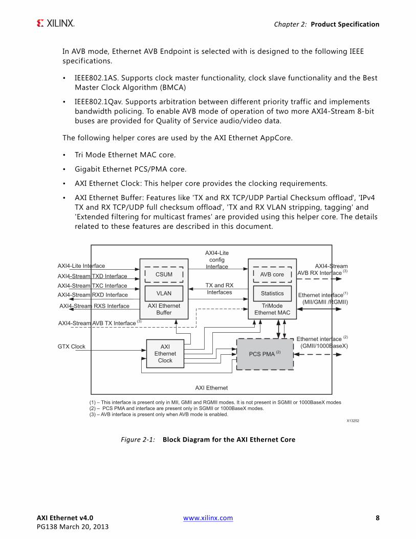
Functional DescriptionA high level block diagram of the AXI Ethernet IP core is shown in Figure 2-1.
The AXI Ethernet core provides an AXI4-Lite bus interface for a simple connection to the MicroBlaze™ processor core to allow access to the registers. The AXI4-Stream 32-bit buses are provided for moving transmit and receive Ethernet data to and from the AXI Ethernet core. These buses are designed to be used with an AXI DMA IP core or any other custom logic in any supported device. The AXI4-Stream buses are designed to provide support for TCP/UDP partial or full checksum off load in hardware if that function is required. The AXI4-Stream buses are described in Frame Transmission in Chapter 2.
The PHY side of the core is connected to an off-the-shelf Ethernet PHY device, which performs the BASE-T standard at 1 Gb/s, 100 Mb/s, and 10 Mb/s speeds. The PHY device can be connected using any of the following supported interfaces: GMII/MII, RGMII, or, by additionally using the 'Ethernet 1000BASE-X PCS/PMA' module for interfaces: SGMII or 1000BaseX.
The supported physical interface types are:
• GMII. The Gigabit Media Independent Interface (GMII) is defined by the IEEE802.3 specification; it can provide support for Ethernet operation at 10 Mb/s, 100 Mb/s and 1 Gb/s speeds.
• MII. The Media Independent Interface (MII) is defined by the IEEE802.3 specif ication; it can provide support for Ethernet operation at 10 Mb/s and 100 Mb/s speeds.
• RGMII. The Reduced Gigabit Media Independent Interface (RGMII) is, effectively, a Double Data Rate version of GMII; it can provide support for Ethernet operation at 10 Mb/s, 100 Mb/s and 1 Gb/s speeds.
• 1000BASE-X. Physical Coding Sublayer (PCS) and Physical Medium Attachment (PMA) operation, as defined in the IEEE 802.3-2008 standard.
• GMII to Serial-GMII (SGMII) bridge or to SGMII bridge. As defined in the Serial-GMII specif ication (ENG-46158).
AXI Ethernet v4.0 www.xilinx.com 8PG138 March 20, 2013
Chapter 2: Product Specification
In AVB mode, Ethernet AVB Endpoint is selected with is designed to the following IEEE specifications.
• IEEE802.1AS. Supports clock master functionality, clock slave functionality and the Best Master Clock Algorithm (BMCA)
• IEEE802.1Qav. Supports arbitration between different priority traff ic and implements bandwidth policing. To enable AVB mode of operation of two more AXI4-Stream 8-bit buses are provided for Quality of Service audio/video data.
The following helper cores are used by the AXI Ethernet AppCore.
• Tri Mode Ethernet MAC core.
• Gigabit Ethernet PCS/PMA core.
• AXI Ethernet Clock: This helper core provides the clocking requirements.
• AXI Ethernet Buffer: Features like 'TX and RX TCP/UDP Partial Checksum offload', 'IPv4 TX and RX TCP/UDP full checksum offload', 'TX and RX VLAN stripping, tagging' and 'Extended filtering for multicast frames' are provided using this helper core. The details related to these features are described in this document.
X-Ref Target - Figure 2-1
Figure 2‐1: Block Diagram for the AXI Ethernet Core

AXI Ethernet v4.0 www.xilinx.com 9PG138 March 20, 2013
Chapter 2: Product Specification
Partial TCP/UDP Checksum Off Load in Hardware
When using TCP or UDP Ethernet protocols, data integrity is maintained by calculating and verifying checksum values over the TCP and UDP frame data. Normally this checksum functionality is handled by the protocol stack software which can be relatively slow and uses signif icant processor power for large frames at high Ethernet data rates. An alternative is to off load some of this transmit checksum generation and receive checksum verif ication in hardware. This is possible by including checksum off-loading in the AXI Ethernet core using the C_TXCSUM and C_RXCSUM parameters. Including the checksum offload functions are a trade-off between using more FPGA resources and getting higher Ethernet performance while freeing up processor use for other functions.
When using the TCP/UDP checksum off load function, checksum information is passed between the software and the AXI Ethernet core, using the AXI4-Stream Control and AXI4-Stream Status interfaces. Table 2-26, Table 2-28, Figure 2-22, Table 2-30, Table 2-31, Table 2-32, Table 2-33, Table 2-34, Table 2-35, and Figure 2-24 show the checksum offload f ields.
The use of the TCP/ UDP checksum offload function requires that the core is connected to the AXI Ethernet core through the AXI4-Stream Control and AXI4-Stream Data interfaces. See Mapping AXI DMA IP Buffer Descriptor Fields to AXI4-Stream Fields for more information.
TX_CSBEGIN is the beginning offset and points to the f irst byte that needs to be included in the checksum calculation. The f irst byte is indicated by a value of zero. The beginning position must be 16-bit aligned. With TCP and UDP, set this value to skip over the Ethernet frame header as well as the IP datagram header. This allows the checksum calculation to start in the correct place of the TCP or UDP segment. Operating systems might provide functions to calculate this value as it is normally based on the variable IP datagram header size. In all cases, the TX_CSBEGIN value must be 14 or larger to be valid.
TX_CSINSERT is the offset which points to the location where the checksum value should be written into the TCP or UDP segment header. This value must be 16-bit aligned and cannot be in the first 8 bytes of the frame. Again, operating systems might provide functions to calculate this value as it is normally variable based on the variable IP datagram header size.
TX_CSCNTRL is a 16-bit f ield; however, only the least significant bit is defined. This bit controls the insertion of the checksum into the frame data. If set to a 1, the checksum value is written into the transmit frame; otherwise, the frame is not modified.
TX_CSINIT is a 16-bit seed that can be used to insert the TCP or UDP pseudo header into the checksum calculation. In many cases the protocol stack calculates the pseudo header checksum value and places it in the header checksum field of the transmit frame. In those cases this f ield should be zeroed.

AXI Ethernet v4.0 www.xilinx.com 10PG138 March 20, 2013
Chapter 2: Product Specification
If the protocol stack does not provide the pseudo header checksum in the header checksum field location of the transmit frame, then that f ield should be zeroed and the pseudo header checksum value must be calculated and placed in the TX_CSINIT f ield of the buffer descriptor.
In order for the transmit checksum to be calculated correctly, the transmit Ethernet FCS must not be provided as part of the transmit data and the transmit FCS calculation and insertion must be enabled in the AXI Ethernet core.
There is a special case for checksums of UDP datagrams. From the UDP RFC 768.
If the computed checksum is zero, it is transmitted as all ones (the equivalent in one’s complement arithmetic). An all zero transmitted checksum value means that the transmitter generated no checksum (for debugging or for higher level protocols that do not care).
If the frame encapsulates a UDP datagram, and if the resulting checksum is zero, a value of all ones is used. This case does not exist for TCP because a checksum of zero is legal; however, the partial checksum logic does not have any way of knowing if the datagram is TCP or UDP.
For both cases, if the computed checksum is zero, a value of all ones is used instead. If a TCP datagram computed checksum is zero, this can result in the packet being dropped by the receiver.
RX_CSRAW is the raw receive checksum calculated over the entire Ethernet payload. It is calculated starting at byte 14 of the Ethernet frame with the count starting at zero, not one (the byte following the Type/Length field) and continues until the end of the Ethernet frame. If the receive Ethernet FCS stripping is not enabled in the AXI Ethernet core, the FCS is also included in the checksum. The application is required to calculate the checksum of the fields which should not have been included to subtract them from the RAW checksum value. In most cases, the protocol software that allows receive checksum offloading requires a pass or fail indication. The application has to compare the adjusted raw checksum value with the checksum field of the TCP or UDP header and provide the pass or fail indication.
Full TCP/UDP Checksum Off Load in Hardware
When using TCP or UDP Ethernet protocols, data integrity is maintained by calculating and verifying checksum values over the TCP and UDP frame data. Normally this checksum functionality is handled by the protocol stack software which can be relatively slow and uses a significant amount of the processor for large frames at high Ethernet data rates.
An alternative is to offload the transmit checksum generation and receive checksum verif ication in hardware. This is possible by including full checksum offloading in the AXI Ethernet core using parameters. Including the full checksum offload functions are a trade-off between using more FPGA resources and getting higher Ethernet performance while freeing up the processor for other functions.

AXI Ethernet v4.0 www.xilinx.com 11PG138 March 20, 2013
Chapter 2: Product Specification
Full checksum offloading is supported for Ethernet II and Sub-Network Access Protocol (SNAP) frame formats. The frame formats must use the IPv4 Internet protocol and transport data through TCP or UDP. Each frame format can support a single 32-bit VLAN tag (the TPID must equal 0x8100). Example diagrams of these frame formats are shown in Figures 2-2 to 2-9. In these figures, the conditions shown in red are used by the hardware to determine if the TCP/UDP checksum and/or the IPv4 Header checksum is calculated.
It is possible for the IPv4 Header checksum to be calculated even though the TCP/UDP checksum is not calculated. This can occur if the frame is Ethernet II or SNAP with an IPv4 Header that is 5 words in length, the IP flags are set to 0, and the fragment offset is set to zero (the protocol f ield can be set to something other than TCP or UDP). However, for the TCP or UDP checksum to be calculated, the IPv4 Header checksum must be calculated with the protocol f ield set to 0x6 for TCP or 0x11 for UDP. Figure 2-2 shows an Ethernet II frame with IPv4 and TCP. The following conditions must be met for the IPv4 Header checksum and TCP checksum to be calculated:
° Type = 0x0800
° Version - 0x4
° Header Length = 0x5
° IP Flag MF = 0b0
° Fragment Offset = 0b0000000000000
° Protocol = 0x06
If Protocol /= 0x06, but the rest of the conditions are met, only the IPv4 Header checksum is calculated.
X-Ref Target - Figure 2-2
Figure 2‐2: Ethernet II Frame with IPv4 and TCP

AXI Ethernet v4.0 www.xilinx.com 12PG138 March 20, 2013
Chapter 2: Product Specification
Figure 2-3 shows a VLAN Ethernet II frame with IPv4 and TCP. The following conditions must be met for the IPv4 Header checksum and TCP checksum to be calculated:
° VLAN TPID = 0x8100
° Type = 0x0800
° Version - 0x4
° Header Length = 0x5
° IP Flag MF = 0b0
° Fragment Offset = 0b0000000000000
° Protocol = 0x06
If Protocol /= 0x06, but the rest of the conditions are met, only the IPv4 Header checksum is calculated.
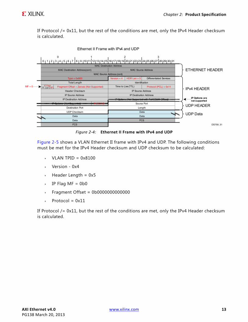
Figure 2-4 shows an Ethernet II frame with IPv4 and UDP. The following conditions must be met for the IPv4 Header checksum and UDP checksum to be calculated:
° Version - 0x4
° Header Length = 0x5
° IP Flag MF = 0b0
° Fragment Offset = 0b0000000000000
° Protocol = 0x11
X-Ref Target - Figure 2-3
Figure 2‐3: VLAN Ethernet II Frame with IPv4 and TCP
AXI Ethernet v4.0 www.xilinx.com 13PG138 March 20, 2013
Chapter 2: Product Specification
If Protocol /= 0x11, but the rest of the conditions are met, only the IPv4 Header checksum is calculated.
Figure 2-5 shows a VLAN Ethernet II frame with IPv4 and UDP. The following conditions must be met for the IPv4 Header checksum and UDP checksum to be calculated:
° VLAN TPID = 0x8100
° Version - 0x4
° Header Length = 0x5
° IP Flag MF = 0b0
° Fragment Offset = 0b0000000000000
° Protocol = 0x11
If Protocol /= 0x11, but the rest of the conditions are met, only the IPv4 Header checksum is calculated.
X-Ref Target - Figure 2-4
Figure 2‐4: Ethernet II Frame with IPv4 and UDP

AXI Ethernet v4.0 www.xilinx.com 14PG138 March 20, 2013
Chapter 2: Product Specification
Figure 2-6 shows a SNAP frame with IPv4 and TCP. The following conditions must be met for the IPv4 Header checksum and TCP checksum to be calculated:
° Length <= 0x0600
° DSAP = 0xAA
° SSAP = 0xAA
° Control = 0x03
° OIU - 0x000000
° Type = 0x0800
° Version - 0x4
° Header Length = 0x5
° IP Flag MF = 0b0
° Fragment Offset = 0b0000000000000
° Protocol = 0x06
If Protocol /= 0x06, but the rest of the conditions are met, only the IPv4 Header checksum is calculated.
X-Ref Target - Figure 2-5
Figure 2‐5: VLAN Ethernet II Frame with IPv4 and UDP

AXI Ethernet v4.0 www.xilinx.com 15PG138 March 20, 2013
Chapter 2: Product Specification
Figure 2-7 shows a VLAN SNAP frame with IPv4 and TCP. The following conditions must be met for the IPv4 Header checksum and TCP checksum to be calculated:
° VLAN TPID = 0x8100
° Length <= 0x0600
° DSAP = 0xAA
° SSAP = 0xAA
° Control = 0x03
° OIU - 0x000000
° Type = 0x0800
° Version - 0x4
° Header Length = 0x5
° IP Flag MF = 0b0
° Fragment Offset = 0b0000000000000
° Protocol = 0x06
If Protocol /= 0x06, but the rest of the conditions are met, only the IPv4 Header checksum is calculated.
X-Ref Target - Figure 2-6
Figure 2‐6: SNAP Frame with IPv4 and TCP

AXI Ethernet v4.0 www.xilinx.com 16PG138 March 20, 2013
Chapter 2: Product Specification
Figure 2-8 shows a SNAP frame with IPv4 and UDP. The following conditions must be met for the IPv4 Header checksum and UDP checksum to be calculated:
° Length <= 0x0600
° DSAP = 0xAA
° SSAP = 0xAA
° Control = 0x03
° OIU - 0x000000
° Type = 0x0800
° Version - 0x4
° Header Length = 0x5
° IP Flag MF =0b0
° Fragment Offset =0b0000000000000
° Protocol = 0x11
If Protocol /= 0x11, but the rest of the conditions are met, only the IPv4 Header checksum is calculated.
X-Ref Target - Figure 2-7
Figure 2‐7: VLAN SNAP Frame with IPv4 and TCP
AXI Ethernet v4.0 www.xilinx.com 17PG138 March 20, 2013
Chapter 2: Product Specification
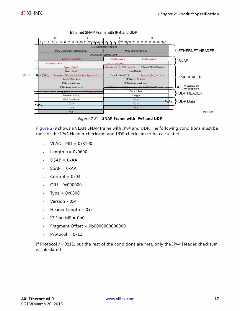
Figure 2-9 shows a VLAN SNAP frame with IPv4 and UDP. The following conditions must be met for the IPv4 Header checksum and UDP checksum to be calculated:
° VLAN TPID = 0x8100
° Length <= 0x0600
° DSAP = 0xAA
° SSAP = 0xAA
° Control = 0x03
° OIU - 0x000000
° Type = 0x0800
° Version - 0x4
° Header Length = 0x5
° IP Flag MF = 0b0
° Fragment Offset = 0b0000000000000
° Protocol = 0x11
If Protocol /= 0x11, but the rest of the conditions are met, only the IPv4 Header checksum is calculated.
X-Ref Target - Figure 2-8
Figure 2‐8: SNAP Frame with IPv4 and UDP

AXI Ethernet v4.0 www.xilinx.com 18PG138 March 20, 2013
Chapter 2: Product Specification
If an Ethernet II frame with protocol information is less than 60 bytes, the transmitter pads the frame with zeroes until it is 60 bytes. Because the Ethernet II frame populates the Type/Length f ield with Type information (0x0800), instead of a Length information, the AXI Ethernet core receive logic is incapable of stripping off any padded bytes. As a result, the receiver reports the length of all transmitter padded packets to be 60 bytes in length.
Frame Transmission
Padding
When fewer than 46 bytes of data are supplied to the AXI Ethernet core, the transmitter adds padding up to the minimum frame length. However, when you are providing the FCS f ield as part of the frame, the frame must already be padded if necessary to maintain the minimum frame length.
X-Ref Target - Figure 2-9
Figure 2‐9: VLAN SNAP Frame with IPv4 and UDP
AXI Ethernet v4.0 www.xilinx.com 19PG138 March 20, 2013
Chapter 2: Product Specification
FCS Pass Through
The AXI Ethernet core can calculate and add the FCS f ield to each transmitted frame or it can pass through a user-supplied FCS f ield with frame data. When a user-supplied FCS f ield is passed through, you must also supply padding as necessary to ensure that the frame meets the minimum frame length requirement. FCS insertion or pass through is controlled by the TC register bit 29 (page 106).
Virtual LAN (VLAN) Frames
When transmitting VLAN frames (if enabled by the TC register bit 27 page 106) without extended VLAN mode, you must supply the VLAN type tag 0x8100 a well as the two byte tag control f ield along with the rest of the frame data. More information about the tag control f ield is available in the IEEE Std 802.3-2008 specification.
Maximum Frame Length and Jumbo Frames
The maximum length of a frame specif ied in the IEEE Std 802.3-2008 specif ication is 1518 bytes for non-VLAN tagged frames. VLAN tagged frames can be extended to 1522 bytes. When jumbo frame handling is disabled (TC register bit 30 page 106) and you attempt to transmit a frame that exceeds the maximum legal length, the AXI Ethernet core inserts an error code to corrupt the current frame and the frame is truncated to the maximum legal length. When jumbo frame handling is enabled, frames longer than the legal maximum are transmitted error free. Jumbo frames are restricted by the AXI Ethernet design to less than 16 KB.
Frame Reception
Frame Reception with Errors
An unsuccessful frame reception (for example, a fragment frame or a frame with an incorrect FCS) is dropped and not passed to the system. A Receive Reject interrupt is activated (see bit 3 in Table 2-42).
FCS Pass Through or Stripping
If the Length/Type f ield has a length interpretation, the received frame can be padded to meet the minimum frame size specif ication. If FCS Pass Through is disabled (RCW1 register bit 29 page 104) and Length/Type f iled error checking is enabled (RCW1 register bit 25 page 104), the padding is stripped along with the FCS f ield and is not passed to you. If FCS Pass Through is disabled (RCW1 register bit 29 page 104) and Length/Type f ield error checking is also disabled, the padding is not stripped and is passed to you but the FCS f ield is stripped and is not passed to you.
If the FCS Pass Through is enabled, any padding is passed to you along with the FCS field. Even though the FCS is passed up to you, it is also verif ied and the frame is dropped if the FCS is incorrect. A Receive Reject interrupt is activated (see bit 3 in Table 2-42).
AXI Ethernet v4.0 www.xilinx.com 20PG138 March 20, 2013
Chapter 2: Product Specification
Virtual LAN (VLAN) Frames
Received VLAN tagged frames are passed to you if VLAN frame reception is enabled (RCW1 register bit 27 page 104). This is the basic native VLAN support provided by the TEMAC core. For more information about extended VLAN functions, see the following sections.
Maximum Frame Length and Jumbo Frames
The maximum length of a frame specif ied in the IEEE Std 802.3-2008 specif ication is 1518 bytes for non-VLAN tagged frames. VLAN tagged frames can be extended to 1522 bytes. When jumbo frame handling is disabled (RCW1 register bit 30 page 104) and a received frame exceeds the maximum legal length, the frame is dropped and a Receive Reject interrupt is activated (see bit 3 in Table 2-42). When jumbo frame handling is enabled, frames longer then the legal maximum are received in the same way as shorter frames. Jumbo frames are restricted by the AXI Ethernet design to less than 16KB.
Length/Type Field Error Checks
Length/Type f ield error checking is specif ied in IEEE Std 802.3. This functionality must be enabled (RCW1 register bit 25 page 104) to comply with this specification. Disabling Length/Type checking is intended only for specif ic applications, such as when using over a proprietary backplane.
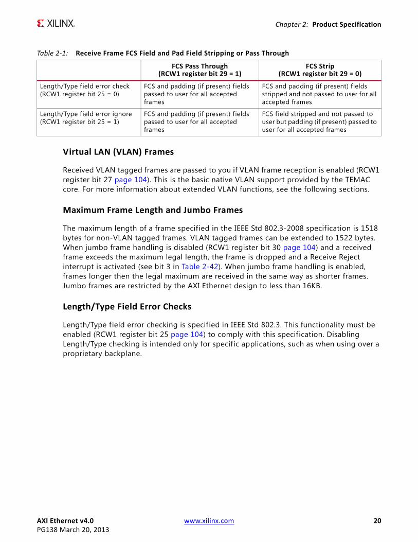
Table 2‐1: Receive Frame FCS Field and Pad Field Stripping or Pass Through
FCS Pass Through(RCW1 register bit 29 = 1)
FCS Strip(RCW1 register bit 29 = 0)
Length/Type f ield error check(RCW1 register bit 25 = 0)
FCS and padding (if present) f ields passed to user for all accepted frames
FCS and padding (if present) f ields stripped and not passed to user for all accepted frames
Length/Type f ield error ignore(RCW1 register bit 25 = 1)
FCS and padding (if present) f ields passed to user for all accepted frames
FCS f ield stripped and not passed to user but padding (if present) passed to user for all accepted frames
AXI Ethernet v4.0 www.xilinx.com 21PG138 March 20, 2013
Chapter 2: Product Specification
Enabled
When Length/Type error checking is enabled, the following checks are made on all frames received. If either of these checks fails, the frame is dropped and a Receive Reject interrupt is activated (see bit 28 in Table 2-42).
• A value greater than or equal to decimal 46 but less than decimal 1536 in the length/type f ield is checked against the actual data length received.
• A value less than decimal 46 in the length/type f ield is checked to ensure the data f ield is padded to exactly 46B. The resultant frame is now the minimum frame size: 64B total in length.
Additionally, if FCS passing is disabled, the length/type f ield is used to strip the FCS f ield and any padding that might exist. Neither is passed to you.
Disabled
When the length/type error checking is disabled, the length/type error checking is not performed and a frame that has only these errors is accepted. Additionally, if FCS passing is disabled, the length/type f ield is not used to determine padding that might exist and the FCS f ield is stripped but any padding that might exist in the frame is not stripped and is passed to you.
Address Filtering
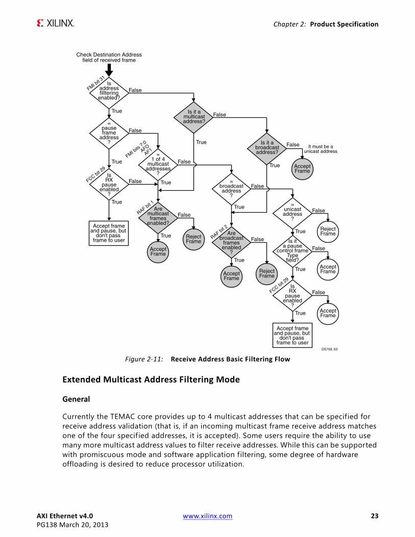
Basic Mode
The receive address filtering function accepts or rejects received frames by examining the destination address f ield. Part of this function is carried out in the TEMAC component and part is carried out based on the bit settings in the Control Register (page 81). Figure 2-11 shows the address f iltering flow.
The decisions shown in white are made in the TEMAC component while the decisions shown in gray are made based on the Control Register settings. The filtering functions includes:
TEMAC component functions
• Programmable unicast destination address matching
• Four programmable multicast address matching
• Broadcast address recognition (0xFFFF_FFFF_FFFF)
• Optional pass through mode with address f ilter disabled (promiscuous mode)
• Pause control frame address recognition (0x0100 00C2 8001)

AXI Ethernet v4.0 www.xilinx.com 22PG138 March 20, 2013
Chapter 2: Product Specification
Control Register enabled functions
• Enable or reject received multicast frames
• Enable or reject received broadcast frames
Receive address filtering eliminates the software overhead required to process frames that are not relevant to a particular Ethernet interface by checking the Destination Address (DA) f ield of the received frame.
The unicast address and multicast addresses are programmed in software through the AXI4-Lite bus as are the Address Filter enable bit, Multicast Address enable bit, and Broadcast Address enable bit. The pause frame address and broadcast address are predefined and do not need programming. See the footnote in Table 2-42, page 87 for a more detailed description on the conditions that can cause the receive reject interrupt to be set.
Using the Address Filters
There are 4, 48-bit (6 byte) registers, that can be used for address f iltering. The address f ilters can be accessed by f irst setting the Filter Mask Index in the Filter Mask Index Register. While the Filter Mask Index is set, the Address Filter Register can be set accessed (Figure 2-10).
X-Ref Target - Figure 2-10
Figure 2‐10: Address Filter Access
AXI Ethernet v4.0 www.xilinx.com 23PG138 March 20, 2013
Chapter 2: Product Specification
Extended Multicast Address Filtering Mode
General
Currently the TEMAC core provides up to 4 multicast addresses that can be specified for receive address validation (that is, if an incoming multicast frame receive address matches one of the four specif ied addresses, it is accepted). Some users require the ability to use many more multicast address values to f ilter receive addresses. While this can be supported with promiscuous mode and software application filtering, some degree of hardware offloading is desired to reduce processor utilization.
X-Ref Target - Figure 2-11
Figure 2‐11: Receive Address Basic Filtering Flow
DS759_63
=1 of 4
multicastaddresses
?
=unicastaddress
?
=broadcastaddress
?
=pauseframe
address?
Isaddressfilltering
enabled?
True
False True
True
True
False
False
False
Aremulticastframes
enabled?
True
FalseFalse
Check Destination Addressfield of received frame
FMI bits
7:0
AFOAF1
FMI bit 3
1
FCC bit 29
FCC bit 29
RAF bit 1
RAF bit 2
False
Arebroadcast
framesenabled
?
True
FalseRejectFrame
RejectFrame
RejectFrame
False
AcceptFrame
False
AcceptFrame
AcceptFrame
AcceptFrame
Is it abroadcastaddress?
True
Is it amulticastaddress?
True
False
False
AcceptFrame
IsRX
pauseenabled
?
True
True
Accept frameand pause, but
don't pass frame to user
Accept frameand pause, but
don't pass frame to user
It must be aunicast address
Is ita pause
control frameTypefield?
True
IsRX
pauseenabled
?
True

AXI Ethernet v4.0 www.xilinx.com 24PG138 March 20, 2013
Chapter 2: Product Specification
Extended multicast f iltering is included at build time by setting the C_MCAST_EXTEND parameter to 1. This provides additional logic for address filtering beyond what is built into the TEMAC core itself. The TEMAC core prevents receiving any multicast frames if they do not match one of the four entries in the built-in multicast address table. As a result, the TEMAC core has to be placed in promiscuous address mode to force it to pass all multicast frames through to the extended multicast address f iltering logic.
With the core in this mode, it also passes through all unicast address frames. To avoid increasing the processor load for unicast address filtering, additional unicast address f iltering has to be added to the extended multicast address f iltering logic. You must make sure that the TEMAC core is in promiscuous receive address mode when using this extended multicast address f iltering mode.
Implementation Details
Received multicast frames that meet all other hardware verif ication requirements receive a f irst level address filtering in hardware. Frames that pass this initial f iltering are passed up to software drivers with information provided by hardware to assist the software drivers in providing the second level/final address f iltering. If the frame does not pass hardware f iltering, the frame is dropped and no action is required by the software drivers.
While a MAC multicast address is defined as any 48-bit MAC address that has bit 0 (LSB) set to 1 (for example 01:00:00:00:00:00), in most cases the MAC multicast address is created from a IP multicast address as shown in Figure 2-12. It is these IP multicast addresses that are a subset of MAC multicast addresses that are f iltered by the extended multicast address f iltering mode.
X-Ref Target - Figure 2-12
Figure 2‐12: Mapping IP Multicast Addresses to MAC Multicast Addresses

AXI Ethernet v4.0 www.xilinx.com 25PG138 March 20, 2013
Chapter 2: Product Specification
When a multicast address frame is received while this extended multicast f iltering is enabled, the AXI Ethernet core f irst verif ies that the f irst 24 bits are 01:00:5E and then uses the upper 15 bits of the unique 23-bit MAC multicast address to index this memory. If the associated memory location contains a 1 then the frame is accepted and passed up to software for a comparison on the full 23-bit address. If the memory location is a 0 or the upper 24 bits are not 01:00:5E then the frame is not accepted and it is dropped. The memory is 1-bit wide but is addressed on 32-bit word boundaries. The memory is 32K deep. This table must be initialized by software using the AXI4-Lite interface
When using the extended multicast address filtering, the TEMAC must be set to promiscuous mode so that all frames are available for f iltering. In this mode the TEMAC no longer checks for a unicast address match. Additional registers are available to provide unicast address filtering while in this mode. Table 2-46 shows the Receive VLAN Tag Register bit definitions and Table 2-47 shows the Unicast Address Word Lower Register bit definitions.
For builds that have the extended multicast address f iltering enabled, promiscuous mode can be achieved by making sure that the TEMAC is in promiscuous mode and by clearing the EMultiFltrEnbl bit (bit 12) in the Reset and Address Filter Register - Offset 0x0000_0000 in Chapter 2.
When a received frame is accepted and passed up to software, additional information is provided in the receive AXI4-Stream Status words to help the software perform the additional address f iltering with less overhead.
Receive AXI4-Stream Status words 0 and 1 include the destination address of the frame and word 2 includes bits to indicate if the frame had a destination address that was the broadcast address, a MAC multicast address, or an IP multicast address (and if none of those bits are set, it was a unicast address). See Mapping AXI DMA IP Buffer Descriptor Fields to AXI4-Stream Fields for more information.
This allows the software to make decisions about the destination address without accessing the address from within the receive AXI4-Stream Data transfer. When using a Xilinx AXI DMA core, this means the information needed by the software for f iltering is in the buffer descriptor and a decision can be made regarding accepting or rejecting the frame without accessing the data buffer itself thus reducing memory access and buffer indexing overhead.
Flow Control
The flow control function is defined by IEEE Std 802.3-2008 Clause 31. The AXI Ethernet core can be configured to send pause frames and to act upon the pause frames received. These two behaviors can be configured independently (asymmetrically). To enable or disable transmit and receive flow control, see the FCC register (page 107).

AXI Ethernet v4.0 www.xilinx.com 26PG138 March 20, 2013
Chapter 2: Product Specification
Flow control can be used to prevent data loss when an Ethernet interface is unable to process frames fast enough to keep up with the rate of frames provided by another Ethernet interface. When this occurs, the Ethernet interface that requires relief can transmit a pause control frame to the link partner to request it cease transmitting for a defined period of time.
Transmitting a Pause Control Frame
For the AXI Ethernet core, a pause frame transmission can be initiated by writing a pause value to the Transmit Pause Frame Register - Offset 0x0000_0004 in Chapter 2 while transmit pause processing is enabled (FCC register bit 30 is 1 page 107).
Requesting the transmit of a pause frame does not interrupt a transmission in progress but the pause frame is transmitted after the frame in progress. A request to transmit a pause frame results in the transmission of a pause frame even if the transmitter itself is already paused due to the reception of a pause frame.
The destination address supplied with the transmitted pause control frame can be set by writing to the RCW0 and RCW1 registers (page 104).
Receiving a Pause Control Frame
When an error free frame is received by AXI Ethernet core, it examines the following information:
1. The destination address field is compared to the pause control address and the configured unicast address.
2. The Length/Type f ield is compared against the control type code (0x8808).
3. The opcode field contents are matched against the pause control opcode (0x0001).
If compare step 2 or 3 fails or if flow control for the receiver is disabled (FCC register bit 29 is 0 page 107), the frame is ignored by the flow control logic and is passed to you. If the frames pass all 3 compare steps and receive flow control is enabled, the pause parameter in the frame is used to inhibit transmitter operation for the time defined in the IEEE Std 802.3-2008 specif ication, a Receive Reject interrupt is activated (see bit 28 in Table 2-42), and the frame is not passed up to software. If the transmitter is paused and a second pause frame is received, the current pause value of the transmitter is replaced with the new pause value received in the new pause frame including a possible value of 0x0.

AXI Ethernet v4.0 www.xilinx.com 27PG138 March 20, 2013
Chapter 2: Product Specification
Extended VLAN Support
VLAN General Information
VLAN (or Virtual Local Area Network) frames are used to segregate Ethernet traff ic within a larger physical LAN. VLAN frames are created by inserting a 4-byte VLAN TAG field in an Ethernet frame where the 2-byte Type/Length f ield would normally occur thus extending the overall frame by 4 bytes. The VLAN TAG field is further broken down into additional f ields as shown in Figure 2-13.
The TEMAC core provides basic VLAN support that can be enabled or disabled independently. This basic support recognizes VLAN frames that have a TPID value of 0x8100. When basic VLAN function is enabled, the TEMAC core allows good VLAN frames with this TPID value to be processed for validation and address f iltering rather than being dropped. However, some applications require using a TPID value other than 0x8100 or have multiple VLAN tags within one frame (referred to as double tagging, triple tagging). Additionally, some common operations are performed on VLAN frames that can be off-loaded from software to hardware to reduce processor utilization. Some of these tasks, translation, stripping, and auto tagging, are available when the extended VLAN support is included in the core at build-time by setting the C_TXVLAN_* and C_RXVLAN_* parameters.
The extended VLAN functions are available individually and independently between the transmit and receive paths. To use the extended VLAN functions, the circuitry must be included at build time by setting the appropriate parameters and also the functions must be enabled at run time by setting the New Functions enable bit (bit 11) of the Reset and Address Filter Register - Offset 0x0000_0000 in Chapter 2.
X-Ref Target - Figure 2-13
Figure 2‐13: VLAN Frame Showing VLAN Tag Field

AXI Ethernet v4.0 www.xilinx.com 28PG138 March 20, 2013
Chapter 2: Product Specification
VLAN Translation
VLAN translation enables the AXI Ethernet core to replace the VLAN ID (VID) value of the VLAN Tag field of a VLAN frame with a new VID as it passes through the AXI Ethernet core in either the transmit or receive direction.
The TEMAC core does not recognize transmitting or receiving VLAN frames with a TPID other than 0x8100 when VLAN mode is enabled. If VLAN mode is disabled, then the maximum length of a normal frame is not extended from 1518 to 1522 bytes. Additionally, multiple tagging is also not supported because of the even larger frame sizes.
To support multiple VLAN tagging and the use of TPID values other than 0x8100 in the outer tag, jumbo frame mode must be used with basic VLAN mode disabled. Using this setting eliminates automatic invalidating (by the TEMAC core) of any frames that normally would be too large for normal frame sizes. You must enable jumbo frame mode and disable VLAN mode when needed for extended VLAN mode.
Transmit Path
When transmitting frames, the outgoing frame is detected as a VLAN frame by recognizing a VLAN Tag Protocol Identif ier value (TPID) in the Type/Length field by comparing it against user defined values in the VLAN TPID Word 0 Register - Offset 0x0000_0028 in Chapter 2 and VLAN TPID Word 1 Register - Offset 0x0000_002C in Chapter 2. The TPID values are shared between the receive and transmit paths.
After a VLAN frame is identif ied, the 12-bit Unique VLAN Identif ier (VID) is used to access the TEMAC Receive Configuration Word 0 Register - Offset 0x0000_0400 in Chapter 2 to supply a replacement VID value which is substituted into the outgoing frame.
X-Ref Target - Figure 2-14
Figure 2‐14: VLAN VID Translation

AXI Ethernet v4.0 www.xilinx.com 29PG138 March 20, 2013
Chapter 2: Product Specification
Using transmit In-Band FCS mode of the TEMAC core is not allowed when using VLAN translation because the user-provided FCS field value will not be correct for the new VID f ield. For double, triple, tagged VLAN frames, only the outer VID is translated. The following TPID values are commonly used to flag VLAN frames: 0x8100, 0x9100, 0x9200, and 0x88a8. However, the TPID values used to identify VLAN frames are programmable through the TPID registers. Transmit and receive VLAN translation can be enabled separately with their respective parameters. For VID values that do not need to be translated, the VLAN data table location associated with their value must be initialized to that same value.
Receive Path
The receive operates similarly to the transmit side. The frame first passes through address f iltering and validation processing before being checked for a VLAN TPID. Receive FCS stripping in the TEMAC core is required when using VLAN translation because the FCS f ield that arrives with the frame is no longer valid with the new TPID value. Although receive stripping is enabled, any padding, if present, is not stripped due to the TYPE/LENGTH field of the receive frame containing a VLAN tag rather than a length value.
X-Ref Target - Figure 2-15
Figure 2‐15: VLAN Data Table

AXI Ethernet v4.0 www.xilinx.com 30PG138 March 20, 2013
Chapter 2: Product Specification
VLAN Tagging and Double Tagging
VLAN tagging, also referred to as "stacking," allows the TEMAC to insert a pre-defined VLAN tag in select Ethernet frames as they pass through the core in either the transmit or receive direction.
One VLAN tag is added depending on mode of operation:
• Non-VLAN frames get one VLAN tag added to become single VLAN tagged frames.
• VLAN tagged frames receive another VLAN tag and no checking is performed to see how many VLAN tags the frame already has (if there are already 3 tags it now has 4).
Therefore, in cases that require adding a VLAN tag, one VLAN tag is added to the existing frame.
The TEMAC core basic VLAN mode extends the maximum normal frame size validation by 4 bytes. This mode does not extend to multiple VLAN tagging. Multiple VLAN frames that exceed 1522 bytes would be discarded as being too long. As mentioned previously, this requires the use of jumbo frame mode which eliminates the automatic invalidation of frames that normally would be too large for normal frame sizes.
When VLAN tagging is enabled at build time with the appropriate parameter, a f ield in the Reset and Address Filter Register - Offset 0x0000_0000 in Chapter 2 is used to select one of four VLAN tagging modes and the Transmit VLAN Tag Register - Offset 0x0000_0018 in Chapter 2 and Receive VLAN Tag Register - Offset 0x0000_001C is used to hold the VLAN tag value which is inserted. The four VLAN tagging modes which are selectable at run time are:
X-Ref Target - Figure 2-16
Figure 2‐16: VLAN Tagging
AXI Ethernet v4.0 www.xilinx.com 31PG138 March 20, 2013
Chapter 2: Product Specification
• Do not add tags to any frames
• Add one tag to all frames
• Add one tag only to frames that are already VLAN tagged
• Add one tag only to select frames that are already VLAN tagged based on VID value
The fourth mode requires a method for specifying which tagged frames should receive an additional VLAN tag. The TEMAC Receive Configuration Word 0 Register - Offset 0x0000_0400 in Chapter 2 and Receive VLAN Data Table - Offset 0x0000_8000-0x0000_BFFF in Chapter 2 are used for this purpose. A “1” in the tag enable f ield for a TPID value indicates that frame should receive an additional tag. Again, transmit In-Band FCS mode is not allowed and receive FCS stripping is required when using VLAN tagging because FCS f ield value will not be correct for the frame with the additional VLAN tag. Although receive stripping is enabled, any padding, if present, is not stripped because the TYPE / LENGTH field of the receive frame contains a VLAN tag rather than a length value. However, the length f ield is still present.
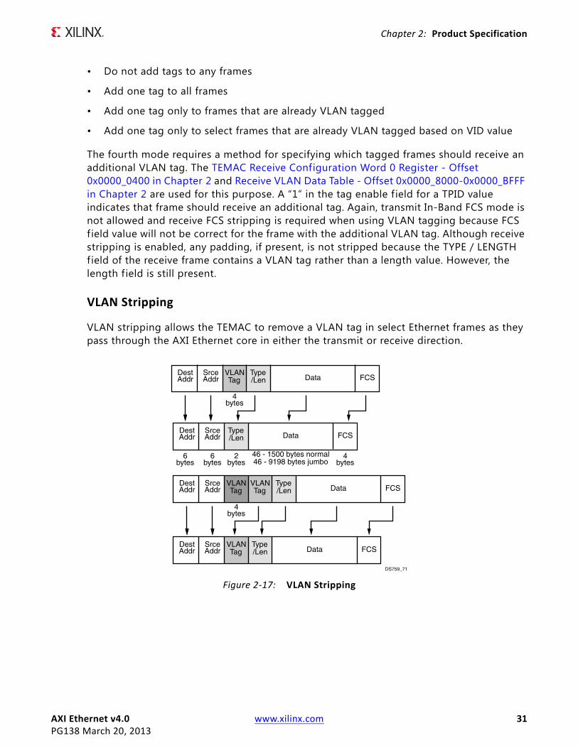
VLAN Stripping
VLAN stripping allows the TEMAC to remove a VLAN tag in select Ethernet frames as they pass through the AXI Ethernet core in either the transmit or receive direction.
X-Ref Target - Figure 2-17
Figure 2‐17: VLAN Stripping
AXI Ethernet v4.0 www.xilinx.com 32PG138 March 20, 2013
Chapter 2: Product Specification
One VLAN tag is removed:
• Non-VLAN frames are not changed.
• VLAN tagged frames have the outer VLAN tag removed and the AXI Ethernet core does not check to see how many VLAN tags it already has (if there are 4 tags, AXI Ethernet core makes it 3).
When VLAN stripping is enabled at build time with the appropriate parameter, a f ield in the Reset and Address Filter Register - Offset 0x0000_0000 in Chapter 2 is used to select one of three VLAN stripping modes.
• Do not strip tags from any frames
• Strip one tag from all VLAN tagged frames
• Strip one tag only from select VLAN tagged frames based on VID value
The third mode requires a method for specifying which tagged frames should be stripped. The TEMAC Receive Configuration Word 0 Register - Offset 0x0000_0400 and Receive VLAN Data Table - Offset 0x0000_8000-0x0000_BFFF in Chapter 2 are used for this purpose. A “1” in the strip enable f ield for a TPID value indicates that frame should have its VLAN tag stripped.
Again, transmit In-Band FCS mode is not allowed and receive FCS stripping is required when using VLAN stripping because FCS f ield value would not be correct for the frame with the VLAN tag removed. Although receive stripping is enabled, any padding, if present, is not stripped due to the TYPE/LENGTH field of the receive frame containing a VLAN tag rather than a length value.
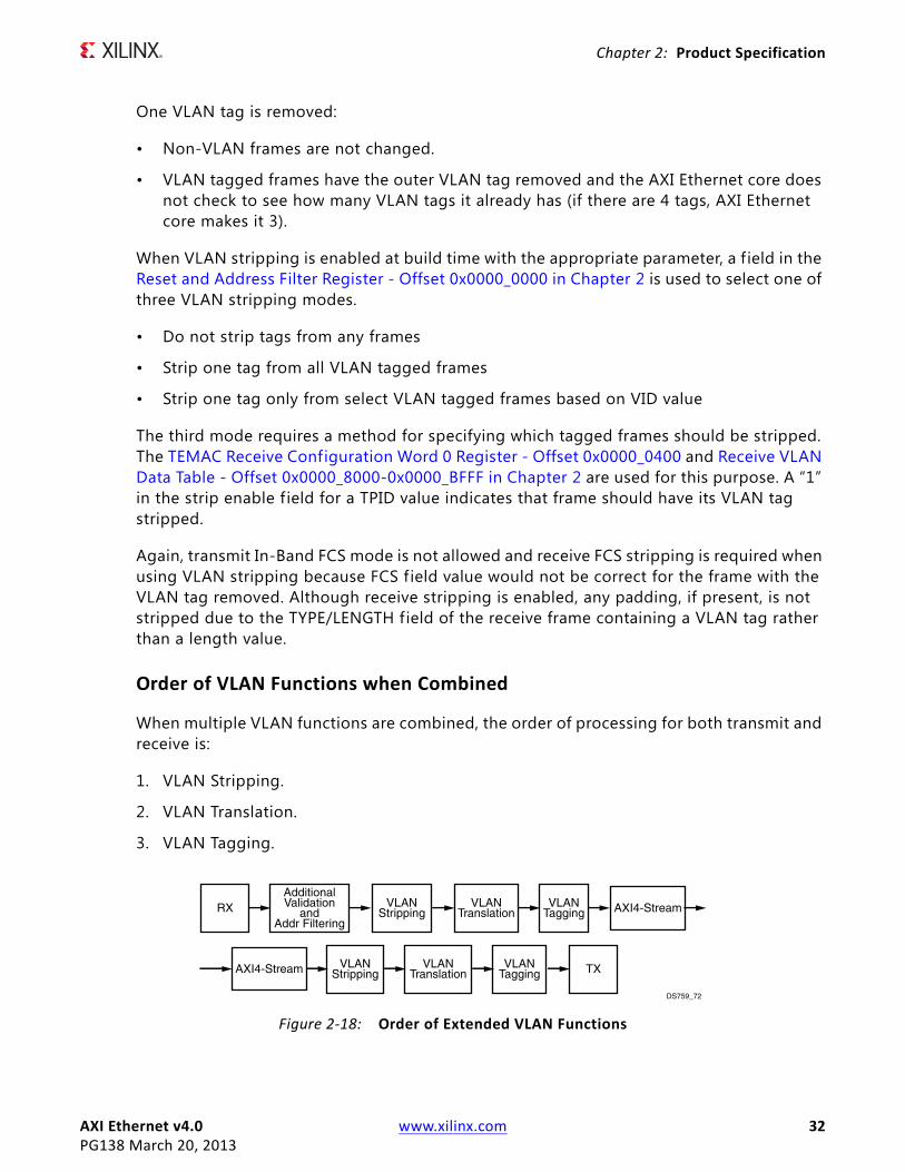
Order of VLAN Functions when Combined
When multiple VLAN functions are combined, the order of processing for both transmit and receive is:
1. VLAN Stripping.
2. VLAN Translation.
3. VLAN Tagging.X-Ref Target - Figure 2-18
Figure 2‐18: Order of Extended VLAN Functions
RXAdditionalValidation
andAddr Filtering
VLANStripping
VLANTranslation
VLANTagging
AXI4-Stream
AXI4-Stream
VLANStripping
VLANTranslation
VLANTagging TX
DS759_72
AXI Ethernet v4.0 www.xilinx.com 33PG138 March 20, 2013
Chapter 2: Product Specification
Using the MII Management to Access Internal or External PHY Registers
The MII Management interface is used to access PHY registers. These PHYs can either be external to the FPGA or, internal to the FPGA. In case of SGMII or 1000BaseX modes, one PHY is present internal to the FPGA. The details of PHY registers can be found in their respective documents. More details are added based on the IEEE standard. For 1000BASE-X PCS/PMA Management Registers. See the LogiCORE IP Ethernet 1000BASE-X PCS/PMA or SGMII Product Guide (PG047).
IMPORTANT: Prior to any MII Management accesses, the MII Management Configuration register must be written with a valid CLOCK_DIVIDE value and the MDIOEN bit must be set.
The value of the PHYAD and REGAD fields in the MII Management Control register determines which PHY registers are accessed. Each PHY, internal or external, should have a unique 5-bit PHY address excluding “00000” which is define as a broadcast PHY address. The MII Management interface is defined in IEEE Std 802.3, Clause 22 as a two-wire interface with a shared bidirectional serial data bus and a clock with a maximum permitted frequency of 2.5 MHz. As a result, MII Management access can take many AXI4-Lite clock cycles to complete.
To write to a PHY register, the data must be written to the MII Management Data Write register. The PHY address (PHYAD) and PHY Register (REGAD) are written to the MII Management Control Register. Setting the Initiate bit in the MII Management Control Register starts the operation. The format of the PHYAD and REGAD in the MII Management Control Register is shown in Figure 2-19.
To read from a PHY register, the PHY address and register number are written to the MII Management Control Register. Setting the Initiate bit in the MII Management Control Register starts the operation. When the operation completes, the PHY register value is available in the MII Management Read Data Register. To access the internal SGMII or 1000BASE-X registers, the PHYAD should match that set by the parameter C_PHYADDR.

AXI Ethernet v4.0 www.xilinx.com 34PG138 March 20, 2013
Chapter 2: Product Specification
Table 2-2 provides an example of a PHY register write through the MII Management Interface.
After a transfer has been initiated on the MDIO interface, it is also possible to access a non-MDIO register in the memory space normally. The MDIO transfer has completed when the RDY bit in the MII Management Control register is 1. This bit can either be polled, or the interrupt can be monitored.
X-Ref Target - Figure 2-19
Figure 2‐19: MII Management Write Register Field Mapping
Table 2‐2: Example of a PHY Register Write via the MII Management Interface
Register Access Value Activity
MIIM Write Data Reg Write 0x0000ABCD Write the value that is written to the PHY register (0xABCD in
this case).
MII ManagementControl Register Write 0x01024800
Initiate the write to the MII Management Control register by setting the PHYAD (00001), REGAD(00010), OP (01), and Initiate bit (1).
MII ManagementControl Register Read 0x01024880 Poll the MII Management Control register bit 7. When set to 1,
the data has been written.
Table 2‐3: Example of a PHY Register Read via the MII Management Interface
Register Access Value Activity
MII ManagementControl Register Write 0x01028800
Initiate the write to the MII Management Control register by setting the PHYAD (00001), REGAD(00001), OP (10), and Initiate bit (1).
MII ManagementControl Register Read 0x01028880 Poll the MII Management Control register bit 7. When set to 1,
the read data is available.
MII ManagementRead Data Register
Read Read data provided by PHY register.

AXI Ethernet v4.0 www.xilinx.com 35PG138 March 20, 2013
Chapter 2: Product Specification
If the MII Management Control register is rewritten in an attempt to start a new transfer, the data is captured; however, the transfer does not take place until the current transaction completes. If the previous transaction was a read, the read data is valid when the first transaction completes. If the previous transaction was a write, the MII Management Write Data register can be written after the f irst transaction completes. The MII Management Control register should be checked to ensure all MDIO transactions have been completed before accessing the data or initiating a transfer.
Serial Gigabit Media Independent Interface
The Serial-GMII (SGMII) is an alternative interface to the GMII/MII that converts the parallel interface of the GMII into a serial format. This radically reduces the I/O count and is therefore often favored by PCB designers. This is achieved by using a serial transceiver. SGMII can carry Ethernet traff ic at 10 Mb/s, 100 Mb/s, and 1 Gb/s.
The SGMII physical interface was defined by Cisco Systems, Inc. The data signals operate at a rate of 1.25 Gb/s. Differential pairs are used to provide signal integrity and minimize noise. The sideband clock signals defined in the specif ication are not implemented in AXI Ethernet core.
Instead, the transceiver is used to transmit and receive the differential data at the required rate using clock data recovery. For more information on SGMII, see the Serial GMII Specification v1.7.
SGMII Auto‐Negotiation
The external SGMII capable PHY device performs auto negotiation with its link partner on the PHY Link (Ethernet bus) resolving operational speed and duplex mode and then in turn performs a secondary auto negotiation with the transceiver across the SGMII Link. This transfers the results of the PHY with Link Partner auto negotiation across the SGMII to the AXI Ethernet core.
The results of the SGMII auto negotiation can be read from the SGMII Management Auto negotiation Link Partner Ability Base Register (Table 2-19). The duplex mode and speed of AXI Ethernet core should then be set to match (see TEMAC Receive Configuration Word 1 Register - Offset 0x0000_0404 in Chapter 2, TEMAC Transmit Configuration Register - Offset 0x0000_0408 in Chapter 2, and TEMAC Ethernet MAC Mode Configuration Register - Offset 0x0000_0410 in Chapter 2).
There are two methods that can be used to learn of the completion of an auto negotiation cycle:
1. Polling the auto negotiation complete bit of SGMII Management Status Register (Register 1, bit 5 Table 2-6, page 38).
2. Using the auto negotiation complete interrupt (Interrupt Status Register - Offset 0x0000_000C in Chapter 2 and SGMII Management Auto Negotiation Interrupt Control Register, (Table 2-15.)
AXI Ethernet v4.0 www.xilinx.com 36PG138 March 20, 2013
Chapter 2: Product Specification
When placed into loopback, data is routed from the transmitter to the receiver path at the last possible point in the PCS/PMA sublayer. This is immediately before the transceiver interface. When placed into loopback, a constant stream of Idle code groups is transmitted through the transceiver.
Loopback in this position allows test frames to be looped back within the system without allowing them to be received by the link partner (the device connected on the other end of the Ethernet. The transmission of Idles allows the link partner to remain in synchronization so that no fault is reported.
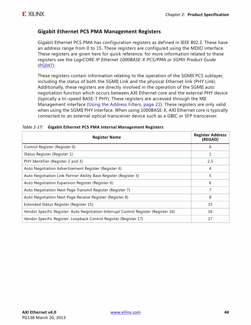
Gigabit Ethernet PCS/PMA Management Registers
Gigabit Ethernet PCS PMA has configuration registers as defined in IEEE 802.3. These have an address range from 0 to 15. These registers are configured using the MDIO interface. These registers are given here for quick reference. For more information related to these registers see LogiCORE IP Ethernet 1000BASE-X PCS/PMA or SGMII Product Guide (PG047)
These registers contain information relating to the operation of the 1000BASE-X PCS/PMA sublayer, including the status of the physical Ethernet link (PHY Link). Additionally, these registers are directly involved in the operation of the 1000BASE-X auto negotiation function which occurs between AXI Ethernet core and its link partner, the Ethernet device connected at the far end of the PHY Link. These registers are accessed through the MII Management interface (Using the Address Filters, page 22). These registers are only valid when using the 1000BASE-X PHY interface.
Table 2‐4: Gigabit Ethernet PCS PMA Internal Management Registers
Register NameRegister Address
(REGAD)
Control Register (Register 0) 0
Status Register (Register 1) 1
PHY Identif ier (Register 2 and 3) 2,3
Auto Negotiation Advertisement Register (Register 4) 4
Auto Negotiation Link Partner Ability Base Register (Register 5) 5
Auto Negotiation Expansion Register (Register 6) 6
Auto Negotiation Next Page Transmit Register (Register 7) 7
Auto Negotiation Next Page Receive Register (Register 8) 8
Extended Status Register (Register 15) 15
Vendor Specific Register: Auto Negotiation Interrupt Control Register (Register 16) 16
Vendor Specific Register: Loopback Control Register (Register 17) 17

AXI Ethernet v4.0 www.xilinx.com 37PG138 March 20, 2013
Chapter 2: Product Specification
Table 2‐5: Control Register (Register 0)
Bits Name Description AttributesDefault Value
15 Reset1 = Core Reset0 = Normal Operation
Read/writeSelf clearing
0
14 Loopback
1 = Enable Loopback Mode0 = Disable Loopback ModeWhen used with a device-specif ic transceiver, the core is placed in internal loopback mode.With the TBI version, Bit 1 is connected to ewrap. When set to ‘1,’ indicates to the external PMA module to enter loopback mode.See Loopback.
Read/write 0
13 Speed Selection (LSB)
Always returns a 0 for this bit. Together with bit 0.6, speed selection of 1000 Mb/s is identif ied
Returns 0 0
12 Auto-Negotiation Enable
1 = Enable Auto-Negotiation Process0 = Disable Auto-Negotiation Process
Read/write 1
11 Power Down
1 = Power down0 = Normal operationWith the PMA option, when set to ’1’ the device-specific transceiver is placed in a low-power state. This bit requires a reset (see bit 0.15) to clear.With the TBI version this register bit has no effect.
Read/ write 0
10 Isolate1 = Electrically Isolate PHY from GMII 0 = Normal operation
Read/write 1
9 Restart Auto- Negotiation
1 = Restart Auto-Negotiation Process0 = Normal Operation
Read/writeSelf clearing
0
8 Duplex Mode Always returns a ‘1’ for this bit to signal Full-Duplex Mode. Returns 1 1
7 Collision Test Always returns a ‘0’ for this bit to disable COL test. Returns 0 0
6 Speed Selection (MSB)
Always returns a ‘1’ for this bit. Together with bit 0.13, speed selection of 1000 Mb/s is identif ied.
Returns 1 1
5 Unidirectional Enable
Enable transmit regardless of whether a valid link has been established. This feature is only possible if Auto-Negotiation Enable bit 0.12 is disabled
Read/ write 0
4-0 Reserved Always return 0s, writes ignored. Returns 0s 00000

AXI Ethernet v4.0 www.xilinx.com 38PG138 March 20, 2013
Chapter 2: Product Specification
Table 2-6 shows the Gigabit Ethernet PCS PMA Management Status Register bit definitions.
Table 2‐6: Management Status Register (Register 1) Bit Definitions
Bits NameCoreAccess
ResetValue
Description
15 100BASE-T4 Returns 0 0 Always returns a 0 for this bit because 100BASE-T4 is not supported.
14 100BASE-XFull Duplex Returns 0 0 Always returns a 0 for this bit because 100BASE-X full duplex is not
supported.
13 100BASE-XHalf Duplex Returns 0 0 Always returns a 0 for this bit because 100BASE-X half duplex is
not supported.
12 10 Mb/sFull Duplex Returns 0 0 Always returns a 0 for this bit because 10 Mb/s full duplex is not
supported.
11 10 Mb/sHalf Duplex Returns 0 0 Always returns a 0 for this bit because 10 Mb/s half duplex is not
supported.
10 100BASE-T2Full Duplex Returns 0 0 Always returns a 0 for this bit because 100BASE-T2 full duplex is
not supported.
9 100BASE-T2Half Duplex Returns 0 0 Always returns a 0 for this bit because 100BASE-T2 half duplex is
not supported.
8 ExtendedStatus Returns 1 1 Always returns a 1 for this bit indicating the presence of the
extended register (register 15).
7 UnidirectionalAbility Returns 1 1 Always returns a 1.
6 MF PreambleSuppression Returns 1 1
Always returns a 1 for this bit to indicate the support of management framepreamble suppression.
5Auto NegotiationComplete
Read 0 0 - auto negotiation process not completed1 - auto negotiation process complete
4 Remote Fault
Read onlyself clearingon read
0 0 - no remote fault condition detected1 - remote fault condition detected
3Auto NegotiationAbility
Returns 1 1 Always returns a 1 for this bit indicating that the PHY is capable of auto negotiation.
2 Link Status
Read onlyself clearingon read
0 0 - PHY Link is down1 - PHY Link is up
1 Jabber Detect Returns 0 0 Always returns a 0 for this bit because no jabber detect is supported.
0 ExtendedCapability Returns 0 0 Always returns a 0 for this bit because no extended register set is
supported.1. When using the 1000Base-X TEMAC core (C_TYPE = 1 and C_PHY_TYPE = 5), set the isolate bit to zero (Control Register 0 bit
10). The core is not operational until this is completed.
AXI Ethernet v4.0 www.xilinx.com 39PG138 March 20, 2013
Chapter 2: Product Specification
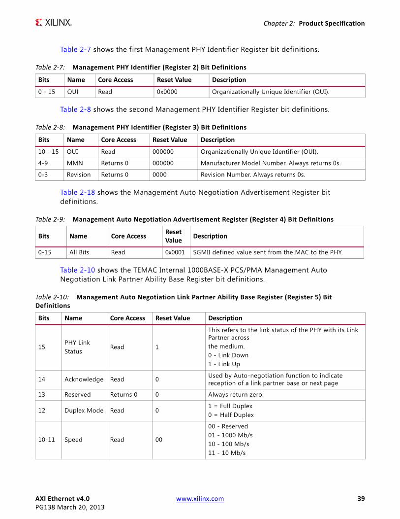
Table 2-7 shows the f irst Management PHY Identif ier Register bit definitions.
Table 2-8 shows the second Management PHY Identif ier Register bit definitions.
Table 2-18 shows the Management Auto Negotiation Advertisement Register bit definitions.
Table 2-10 shows the TEMAC Internal 1000BASE-X PCS/PMA Management Auto Negotiation Link Partner Ability Base Register bit definitions.
Table 2‐7: Management PHY Identifier (Register 2) Bit Definitions
Bits Name Core Access Reset Value Description
0 - 15 OUI Read 0x0000 Organizationally Unique Identif ier (OUI).
Table 2‐8: Management PHY Identifier (Register 3) Bit Definitions
Bits Name Core Access Reset Value Description
10 - 15 OUI Read 000000 Organizationally Unique Identif ier (OUI).
4-9 MMN Returns 0 000000 Manufacturer Model Number. Always returns 0s.
0-3 Revision Returns 0 0000 Revision Number. Always returns 0s.
Table 2‐9: Management Auto Negotiation Advertisement Register (Register 4) Bit Definitions
Bits Name Core AccessReset Value
Description
0-15 All Bits Read 0x0001 SGMII defined value sent from the MAC to the PHY.
Table 2‐10: Management Auto Negotiation Link Partner Ability Base Register (Register 5) Bit Definitions
Bits Name Core Access Reset Value Description
15PHY LinkStatus
Read 1
This refers to the link status of the PHY with its Link Partner acrossthe medium.0 - Link Down1 - Link Up
14 Acknowledge Read 0 Used by Auto-negotiation function to indicate reception of a link partner base or next page
13 Reserved Returns 0 0 Always return zero.
12 Duplex Mode Read 01 = Full Duplex0 = Half Duplex
10-11 Speed Read 00
00 - Reserved01 - 1000 Mb/s10 - 100 Mb/s11 - 10 Mb/s

AXI Ethernet v4.0 www.xilinx.com 40PG138 March 20, 2013
Chapter 2: Product Specification
Table 2-11 shows the Management Auto Negotiation Expansion Register bit definitions.
Table 2-12 shows the Management Auto Negotiation Next Page Transmit Register bit definitions.
Table 2-13 shows the Management Auto Negotiation Next Page Receive Register bit definitions.
1-9 Reserved Returns 0s 000000000 Always return zeros.
0 Reserved Returns 1 1 Always return one.
Table 2‐10: Management Auto Negotiation Link Partner Ability Base Register (Register 5) Bit Definitions (Cont’d)
Bits Name Core Access Reset Value Description
Table 2‐11: Management Auto Negotiation Expansion Register (Register 6) Bit Definitions
Bits Name Core AccessResetValue
Description
3 - 15 Reserved Returns 0s 0x0 Always return zeros.
2 Next Page Able Returns 1 1 Always returns a 1 for this bit because the device is Next Page
Able.
1 Page Received
Read selfclearing on read
0 0 - a new page is not received1 - a new page is received
0 Reserved Returns 0s 0 Always return zeros.
Table 2‐12: Management Auto Negotiation Next Page Transmit Register (Register 7) Bit Definitions
Bits NameCoreAccess
Reset Value Description
15 Next Page Read/write 0 0 - last page1 - additional next pages to follow
14 Reserved Returns 0s 0 Always return zeros.
13 Message Page Read/Write 1 0 - unformatted page1 - message page
12 Acknowledge 2 Read/Write 0 0 - cannot comply with message1 - complies with message
11 Toggle Read 0 Value toggles between subsequent pages.
0 -10Message or unformatted Code Field
Read/Write0x001 (nullmessage code)
Message code f ield or unformatted page encoding as dictated by bit 13.
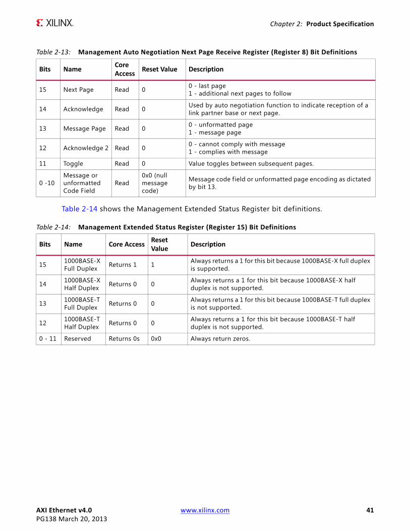
AXI Ethernet v4.0 www.xilinx.com 41PG138 March 20, 2013
Chapter 2: Product Specification
Table 2-14 shows the Management Extended Status Register bit definitions.
Table 2‐13: Management Auto Negotiation Next Page Receive Register (Register 8) Bit Definitions
Bits NameCoreAccess
Reset Value Description
15 Next Page Read 0 0 - last page1 - additional next pages to follow
14 Acknowledge Read 0 Used by auto negotiation function to indicate reception of a link partner base or next page.
13 Message Page Read 0 0 - unformatted page1 - message page
12 Acknowledge 2 Read 0 0 - cannot comply with message1 - complies with message
11 Toggle Read 0 Value toggles between subsequent pages.
0 -10Message orunformattedCode Field
Read0x0 (nullmessage code)
Message code field or unformatted page encoding as dictated by bit 13.
Table 2‐14: Management Extended Status Register (Register 15) Bit Definitions
Bits Name Core AccessReset Value
Description
15 1000BASE-XFull Duplex Returns 1 1 Always returns a 1 for this bit because 1000BASE-X full duplex
is supported.
14 1000BASE-XHalf Duplex Returns 0 0 Always returns a 1 for this bit because 1000BASE-X half
duplex is not supported.
13 1000BASE-TFull Duplex Returns 0 0 Always returns a 1 for this bit because 1000BASE-T full duplex
is not supported.
12 1000BASE-THalf Duplex Returns 0 0 Always returns a 1 for this bit because 1000BASE-T half
duplex is not supported.
0 - 11 Reserved Returns 0s 0x0 Always return zeros.

AXI Ethernet v4.0 www.xilinx.com 42PG138 March 20, 2013
Chapter 2: Product Specification
Table 2-15 shows the Management Auto Negotiation Interrupt Control Register bit definitions.
1000BASE‐X PCS/PMA
PCS/PMA
The Physical Coding Sublayer (PCS) for 1000BASE-X operation is defined in IEEE 802.3 clause 36 and 37 and performs the following:
• Encoding (and decoding) of GMII data octets to form a sequence of ordered sets
• 8B/10B encoding (and decoding) of the sequence ordered sets
• 1000BASE-X Auto-Negotiation for information exchange with the link partner
The Physical Medium Attachment (PMA) for 1000BASE-X operation is defined in IEEE 802.3 clause 36 and performs the following:
• Serialization (and de serialization) of code-groups for transmission (and reception) on the underlying serial PMD sublayer
• Recovery of clock from the 8B/10B coded data supplied by the PMD sublayer
Table 2‐15: Management Auto Negotiation Interrupt Control Register (Register 16) Bit Definitions
Bits NameCore Access
Reset Value
Description
2 - 15 Reserved Returns 0s 0 Always return zeros.
1 Interrupt Status Read/Write 0
If the interrupt is enabled, this bit is asserted upon the completion of an auto negotiation cycle; it is only cleared by writing 0 to this bit. If the interrupt is disabled, this bit is set to 0. This is the auto negotiation complete interrupt.0 - interrupt is asserted1 - interrupt is not asserted
0 Interrupt Enable Read/Write 1 0 - interrupt is disabled
1 - interrupt is enabled
Table 2‐16: Management Loopback Control Register (Register 17) Bit Definitions
Bits Name Core AccessReset Value
Description
1-15 Reserved Returns 0s 0 Always return zeros.
0LoopbackPosition
Read/Write 0
Loopback is enabled or disabled using register 0 bit 14.0 - loopback (when enabled) occurs directly before the interface to the GTX transceiver1 - loopback (when enabled) occurs in the GTX transceiver

AXI Ethernet v4.0 www.xilinx.com 43PG138 March 20, 2013
Chapter 2: Product Specification
1000BASE-X PCS/PMA functionality is provided by connecting the TEMAC silicon component to a GTP transceiver.
PMD
The Physical Medium Dependent (PMD) sublayer is defined in IEEE 802.3 clause 38 for 1000BASE-LX and 1000BASE-SX (long and short wave laser). This type of PMD sublayer is provided by the external GBIC or SFP optical transceiver which should be connected directly to the ports of the GTX transceiver.
1000BASE‐X Auto‐Negotiation
1000BASE-X auto negotiation is described in IEEE Std 802.3, clause 37. This function allows a device to advertise the supported modes of operation to a device at the remote end of a link segment (the link partner on Ethernet), and detect corresponding operational modes advertised by the link partner. The results of the auto negotiation can be read from the 1000BASE-X Management Auto negotiation Link Partner Ability Base Register (Table 2-10). The duplex mode and speed of the AXI Ethernet core should then be set to match (see TEMAC Receive Configuration Word 1 Register - Offset 0x0000_0404, TEMAC Transmit Configuration Register - Offset 0x0000_0408, and TEMAC Ethernet MAC Mode Configuration Register - Offset 0x0000_0410).
There are two methods that can be used to learn of the completion of an auto negotiation cycle:
1. By polling the auto negotiation complete bit of 1000BASE-X Management Status Register (Register 1, bit 5 Table 2-6).
2. By using the auto negotiation complete interrupt (Interrupt Status Register - Offset 0x0000_000C, page 86 and 1000BASE-X Management Auto Negotiation Interrupt Control Register Table 2-15.)
When placed into loopback, data is routed from the transmitter to the receiver path at the last possible point in the PCS/PMA sublayer. This is immediately before the transceiver interface. When placed into loopback, a constant stream of Idle code groups is transmitted through the transceiver. Loopback in this position allows test frames to be looped back within the system without allowing them to be received by the link partner (the device connected on the other end of the Ethernet. The transmission of Idles allows the link partner to remain in synchronization so that no fault is reported.
Loopback can be enabled or disabled by writing to the 1000BASE-X Management Control Register bit 14 (Table 2-6, page 38).
AXI Ethernet v4.0 www.xilinx.com 44PG138 March 20, 2013
Chapter 2: Product Specification
Gigabit Ethernet PCS PMA Management Registers
Gigabit Ethernet PCS PMA has configuration registers as defined in IEEE 802.3. These have an address range from 0 to 15. These registers are configured using the MDIO interface. These registers are given here for quick reference. for more information related to these registers see the LogiCORE IP Ethernet 1000BASE-X PCS/PMA or SGMII Product Guide (PG047).
These registers contain information relating to the operation of the SGMII PCS sublayer, including the status of both the SGMII Link and the physical Ethernet link (PHY Link). Additionally, these registers are directly involved in the operation of the SGMII auto negotiation function which occurs between AXI Ethernet core and the external PHY device (typically a tri-speed BASE-T PHY). These registers are accessed through the MII Management interface (Using the Address Filters, page 22). These registers are only valid when using the SGMII PHY interface. When using 1000BASE-X, AXI Ethernet core is typically connected to an external optical transceiver device such as a GBIC or SFP transceiver.
Table 2‐17: Gigabit Ethernet PCS PMA Internal Management Registers
Register NameRegister Address
(REGAD)
Control Register (Register 0) 0
Status Register (Register 1) 1
PHY Identif ier (Register 2 and 3) 2,3
Auto Negotiation Advertisement Register (Register 4) 4
Auto Negotiation Link Partner Ability Base Register (Register 5) 5
Auto Negotiation Expansion Register (Register 6) 6
Auto Negotiation Next Page Transmit Register (Register 7) 7
Auto Negotiation Next Page Receive Register (Register 8) 8
Extended Status Register (Register 15) 15
Vendor Specific Register: Auto Negotiation Interrupt Control Register (Register 16) 16
Vendor Specific Register: Loopback Control Register (Register 17) 17

AXI Ethernet v4.0 www.xilinx.com 45PG138 March 20, 2013
Chapter 2: Product Specification
Table 2‐18: Management Auto Negotiation Advertisement Register (Register 4) Bit Definitions
Bits Name Core Access Reset Value Description
15 Next Page Read/Write 00 - next page functionality is not advertised1 - next page functionality is advertised
14 Reserved Returns 0s 0 Always return zeros.
12-13RemoteFault
Read/Write selfclearing afterauto negotiation
0x0
00 - no error01 - offline10 - link failure11 - auto negotiation error
9-11 Reserved Returns 0s 0x0 Always return zeros.
7-8 Pause Read/Write 0x3
00 - No pause01 - Symmetric pause10 - Asymmetric pause towards link partner11 - both symmetric pause and asymmetric pause towards link partner
6 Half Duplex Returns 0s 0 Always return zeros because half duplex is not supported.
5 Full Duplex Read/Write 10 - full duplex mode is not advertised1 - full duplex mode is advertised
0-4 Reserved Returns 0s 0x0 Always return zeros.
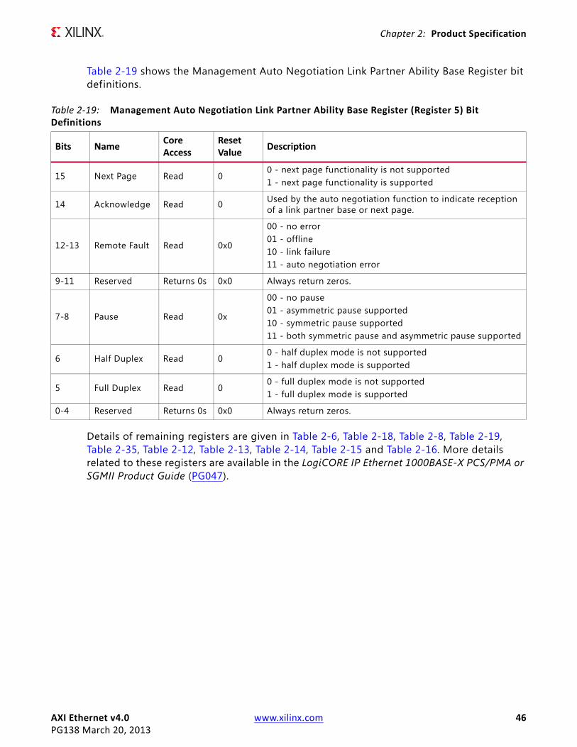
AXI Ethernet v4.0 www.xilinx.com 46PG138 March 20, 2013
Chapter 2: Product Specification
Table 2-19 shows the Management Auto Negotiation Link Partner Ability Base Register bit definitions.
Details of remaining registers are given in Table 2-6, Table 2-18, Table 2-8, Table 2-19, Table 2-35, Table 2-12, Table 2-13, Table 2-14, Table 2-15 and Table 2-16. More details related to these registers are available in the LogiCORE IP Ethernet 1000BASE-X PCS/PMA or SGMII Product Guide (PG047).
Table 2‐19: Management Auto Negotiation Link Partner Ability Base Register (Register 5) Bit Definitions
Bits NameCoreAccess
ResetValue
Description
15 Next Page Read 00 - next page functionality is not supported1 - next page functionality is supported
14 Acknowledge Read 0 Used by the auto negotiation function to indicate reception of a link partner base or next page.
12-13 Remote Fault Read 0x0
00 - no error01 - offline10 - link failure11 - auto negotiation error
9-11 Reserved Returns 0s 0x0 Always return zeros.
7-8 Pause Read 0x
00 - no pause01 - asymmetric pause supported10 - symmetric pause supported11 - both symmetric pause and asymmetric pause supported
6 Half Duplex Read 00 - half duplex mode is not supported1 - half duplex mode is supported
5 Full Duplex Read 00 - full duplex mode is not supported1 - full duplex mode is supported
0-4 Reserved Returns 0s 0x0 Always return zeros.

AXI Ethernet v4.0 www.xilinx.com 47PG138 March 20, 2013
Chapter 2: Product Specification
StandardsThis section describes the standards that are supported by the AXI Ethernet IP core.
• GMII. The Gigabit Media Independent Interface (GMII) is defined by the IEEE802.3 specification; it can provide support for Ethernet operation at 10 Mb/s, 100 Mb/s and 1 Gb/s speeds.
• MII. The Media Independent Interface (MII) is defined by the IEEE802.3 specification; it can provide support for Ethernet operation at 10 Mb/s and 100 Mb/s speeds.
• 1000BASE-X Physical Coding Sublayer (PCS), Physical Medium Attachment (PMA), and RGMII operation, as defined in the IEEE 802.3-2008 standard
• GMII to Serial-GMII (SGMII) bridge or SGMII to GMII bridge, as defined in the Serial-GMII specif ication (ENG-46158)
• Reduced Gigabit Media Independent Interface (RGMII), version 2.0
• IEEE802.1AS Supports clock master functionality, clock slave functionality and the Best Master Clock Algorithm (BMCA)
• IEEE802.1Qav Supports arbitration between different priority traff ic and implements bandwidth policing.
These standards are implemented by the respective helper cores used in this AXI Ethernet core. For more details related to these, see LogiCORE IP Tri-Mode Ethernet MAC Product Guide (PG051) and LogiCORE IP Ethernet 1000BASE-X PCS/PMA or SGMII Product Guide (PG047).
PerformanceTo measure the system performance (FMAX) of the AXI Ethernet core, a system was built in which it was added to each of the supported device families as the Device Under Test (DUT) as shown in Figure 2-20; the AXI Ethernet core represents the DUT block in Figure 2-20.
Because the AXI Ethernet core is used with other design modules in the FPGA, the utilization and timing numbers reported in this section are estimates only. When this core is combined with other designs in the system, the utilization of FPGA resources and timing of the core design can vary from the results reported here.
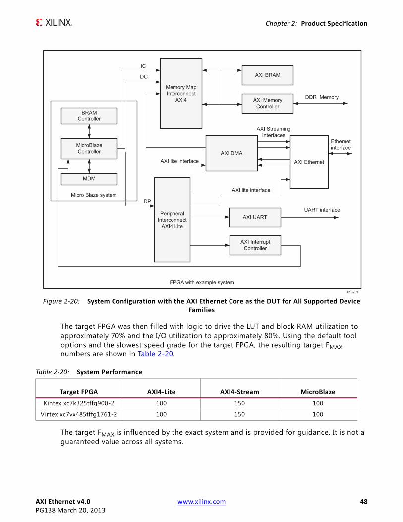
AXI Ethernet v4.0 www.xilinx.com 48PG138 March 20, 2013
Chapter 2: Product Specification
The target FPGA was then f illed with logic to drive the LUT and block RAM utilization to approximately 70% and the I/O utilization to approximately 80%. Using the default tool options and the slowest speed grade for the target FPGA, the resulting target FMAX numbers are shown in Table 2-20.
The target FMAX is influenced by the exact system and is provided for guidance. It is not a guaranteed value across all systems.
X-Ref Target - Figure 2-20
Figure 2‐20: System Configuration with the AXI Ethernet Core as the DUT for All Supported Device Families
Table 2‐20: System Performance
Target FPGA AXI4‐Lite AXI4‐Stream MicroBlaze
Kintex xc7k325tffg900-2 100 150 100
Virtex xc7vx485tffg1761-2 100 150 100
AXI Ethernet v4.0 www.xilinx.com 49PG138 March 20, 2013
Chapter 2: Product Specification
As the AXI Ethernet IP core represents a hierarchical design block containing multiple LogiCORE™ IP instances, the latency, max frequency, throughput and power are provided by the IP instances that are present in a given configuration.
Resource UtilizationThese values were generated using the Vivado™ IP catalog. They are derived from post-synthesis reports, and might change during MAP and PAR.
Because the AXI Ethernet core is a module that is used with other designs in the FPGA, the utilization and timing numbers reported in this section are estimates and can vary from the results reported here. AXI Ethernet core benchmarks for different systems are shown in Table 2-21 for Zynq™-7000, Table 2-22 for Virtex®-7, Table 2-23 for Kintex™-7, and Table 2-24 for Artix™-7 devices.
AXI Ethernet v4.0 www.xilinx.com 50PG138 March 20, 2013
Chapter 2: Product Specification
Table 2‐21: Zynq‐7000 Device Performance and Resource Utilization Benchmarks (xc7z045ffg900‐2)
Configuration Resources
PHY_TY
PE
ENABLE_A
VB
TXCSU
M RXCSU
M
TXVLA
N_TRAN RXVLA
N_TRAN
TXVLA
N_TAG R
XVLA
N_TAG
TXVLA
N_STR
P RXVLA
N_STR
P
MCAST_EXTEND
TX RX M
EM
LUT as Logic
LUT as Distributed RAM
LUT as Shift Register
Register as Flip
‐Flop
Register as Latch
RAMB36:FIFO36
RAMB18:FIFO18
DSPs
1000Basex FALSE None 1 0 1 0 4k 4197 344 56 6266 0 6 2 0
1000Basex FALSE None 1 1 0 1 4k 4411 344 54 6483 0 7 2 0
1000Basex FALSE Full 0 0 0 0 4k 5037 344 51 6585 0 4 0 0
1000Basex TRUE Full 0 0 1 0 4k 5525 440 75 8518 0 6 2 1
GMII FALSE None 0 0 0 1 4k 3436 344 28 5316 0 5 0 0
GMII FALSE Full 0 0 0 0 4k 4437 344 30 5817 0 4 0 0
GMII FALSE None 1 0 0 0 4k 3505 344 33 5467 0 6 2 0
GMII FALSE None 0 1 0 0 4k 3603 344 33 5535 0 4 2 0
GMII FALSE None 0 0 1 0 4k 3518 344 32 5437 0 4 2 0
1000Basex FALSE None 0 0 0 1 4k 4048 344 49 6084 0 5 0 0
RGMII FALSE None 0 0 0 1 4k 4088 394 48 6286 0 5 0 0
RGMII FALSE Full 0 0 0 0 4k 5098 394 50 6787 0 4 0 0
RGMII FALSE None 1 0 1 0 4k 4267 394 55 6468 0 6 2 0
RGMII FALSE None 0 1 0 0 4k 4274 394 53 6505 0 4 2 0
GMII TRUE None 0 0 0 0 4k 5543 490 73 8604 0 6 0 1
SGMII FALSE None 0 0 0 1 4k 3840 394 33 6287 0 5 0 0
SGMII FALSE Full 0 0 0 0 4k 4770 394 34 6812 0 4 0 0
SGMII FALSE None 1 0 1 0 4k 4058 394 36 6483 0 6 2 0
SGMII FALSE None 0 1 0 0 4k 4117 394 37 6517 0 4 2 0
MII FALSE None 0 0 0 1 4k 3252 344 26 5287 0 5 0 0
MII FALSE Full 0 0 0 0 4k 4185 344 27 5812 0 4 0 0
MII FALSE None 1 0 0 0 4k 3497 344 29 5449 0 6 2 0
MII FALSE None 0 1 0 0 4k 3530 344 29 5517 0 4 2 0
MII FALSE None 0 0 1 0 4k 3400 344 29 5419 0 4 2 0
SGMII TRUE None 0 0 0 0 4k 5291 490 47 8595 0 6 0 1

AXI Ethernet v4.0 www.xilinx.com 51PG138 March 20, 2013
Chapter 2: Product Specification
Table 2‐22: Virtex‐7 FPGA Performance and Resource Utilization Benchmarks (xc7vx485tffg1761‐2)
Configuration Resources
PHY_TYPE
ENABLE_A
VB
TXCSU
M RXCSU
M
TXVLA
N_TRAN RXVLA
N_TRAN
TXVLA
N_TAG R
XVLA
N_TAG
TXVLA
N_STR
P RXVLA
N_STR
P
MCAST_EXTEND
TX RX M
EM
LUT as Logic
LUT as Distributed RAM
LUT as Shift Register
Register as Flip
‐Flop
Register as Latch
RAMB36:FIFO36
RAMB18:FIFO18
DSPs
1000Basex FALSE None 1 0 1 0 4k 4201 344 56 6266 0 6 2 0
1000Basex FALSE None 1 1 0 1 4k 4417 344 54 6483 0 7 2 0
1000Basex FALSE Full 0 0 0 0 4k 5041 344 51 6585 0 4 0 0
1000Basex TRUE Full 0 0 1 0 4k 5525 440 75 8518 0 6 2 1
RGMII FALSE None 0 0 0 1 4k 3464 344 28 5335 0 5 0 0
RGMII FALSE Full 0 0 0 0 4k 4463 344 30 5836 0 4 0 0
RGMII FALSE None 1 0 1 0 4k 3613 344 35 5517 0 6 2 0
RGMII FALSE None 0 1 0 0 4k 3627 344 33 5554 0 4 2 0
GMII FALSE None 0 0 0 1 4k 3440 344 28 5316 0 5 0 0
GMII FALSE Full 0 0 0 0 4k 4441 344 30 5817 0 4 0 0
GMII FALSE None 1 0 0 0 4k 3508 344 33 5467 0 6 2 0
GMII FALSE None 0 1 0 0 4k 3603 344 33 5535 0 4 2 0
GMII FALSE None 0 0 1 0 4k 3519 344 32 5437 0 4 2 0
GMII TRUE None 0 0 0 0 4k 4906 440 133 7984 0 6 0 1
1000Basex FALSE None 0 0 0 1 4k 4052 344 49 6084 0 5 0 0
SGMII FALSE None 0 0 0 1 4k 3844 394 33 6287 0 5 0 0
SGMII FALSE Full 0 0 0 0 4k 4772 394 35 6812 0 4 0 0
SGMII FALSE None 1 0 1 0 4k 4061 394 36 6483 0 6 2 0
SGMII FALSE None 0 1 0 0 4k 3253 344 26 5287 0 5 0 0
MII FALSE None 0 0 0 1 4k 4191 344 28 5812 0 4 0 0
MII FALSE Full 0 0 0 0 4k 3501 344 28 5449 0 6 2 0
MII FALSE None 1 0 0 0 4k 3539 344 30 5517 0 4 2 0
MII FALSE None 0 1 0 0 4k 3408 344 28 5419 0 4 2 0
MII FALSE None 0 0 1 0 4k 3408 344 28 5419 0 4 2 0
SGMII TRUE None 0 0 0 0 4k 5290 490 48 8595 0 6 0 1

AXI Ethernet v4.0 www.xilinx.com 52PG138 March 20, 2013
Chapter 2: Product Specification
Table 2‐23: Kintex‐7 FPGA Performance and Resource Utilization Benchmarks (xc7k325tffg900‐2)
Configuration Resources
PHY_TYPE
ENABLE_A
VB
TXCSU
M RXCSU
M
TXVLA
N_TRAN RXVLA
N_TRAN
TXVLA
N_TAG R
XVLA
N_TAG
TXVLA
N_STR
P RXVLA
N_STR
P
MCAST_EXTEND
TX RX M
EM
LUT as Logic
LUT as Distributed RAM
LUT as Shift Register
Register as Flip
‐Flop
Register as Latch
RAMB36:FIFO36
RAMB18:FIFO18
DSPs
1000Basex FALSE None 1 0 1 0 4k 4203 344 56 6266 0 6 2 0
1000Basex FALSE None 1 1 0 1 4k 4415 344 54 6483 0 7 2 0
1000Basex FALSE Full 0 0 0 0 4k 5038 344 51 6585 0 4 0 0
1000Basex TRUE Full 0 0 1 0 4k 5528 440 75 8518 0 6 2 1
RGMII FALSE None 0 0 0 1 4k 3478 344 28 5353 0 5 0 0
RGMII FALSE Full 0 0 0 0 4k 4479 344 30 5854 0 4 0 0
RGMII FALSE None 1 0 1 0 4k 3630 344 35 5535 0 6 2 0
RGMII FALSE None 0 1 0 0 4k 3644 344 33 5572 0 4 2 0
GMII FALSE None 0 0 0 1 4k 3441 344 28 5316 0 5 0 0
GMII FALSE Full 0 0 0 0 4k 4442 344 30 5817 0 4 0 0
GMII FALSE None 1 0 0 0 4k 3509 344 33 5467 0 6 2 0
GMII FALSE None 0 1 0 0 4k 3607 344 33 5535 0 4 2 0
GMII FALSE None 0 0 1 0 4k 3520 344 32 5437 0 4 2 0
GMII TRUE None 0 0 0 0 4k 4908 440 133 7984 0 6 0 1
1000Basex FALSE None 0 0 0 1 4k 4051 344 49 6084 0 5 0 0
SGMII FALSE None 0 0 0 1 4k 4773 394 35 6812 0 4 0 0
SGMII FALSE Full 0 0 0 0 4k 4773 394 35 6812 0 4 0 0
SGMII FALSE None 1 0 1 0 4k 4064 394 36 6483 0 6 2 0
SGMII FALSE None 0 1 0 0 4k 4124 394 36 6517 0 4 2 0
MII FALSE None 0 0 0 1 4k 3256 344 26 5287 0 5 0 0
MII FALSE Full 0 0 0 0 4k 4192 344 27 5812 0 4 0 0
MII FALSE None 1 0 0 0 4k 3494 344 29 5449 0 6 2 0
MII FALSE None 0 1 0 0 4k 3535 344 29 5517 0 4 2 0
MII FALSE None 0 0 1 0 4k 3407 344 29 5419 0 4 2 0
SGMII TRUE None 0 0 0 0 4k 5296 490 48 8595 0 6 0 1
AXI Ethernet v4.0 www.xilinx.com 53PG138 March 20, 2013
Chapter 2: Product Specification
Table 2‐24: Artix‐7 FPGA Performance and Resource Utilization Benchmarks (xc7a200tffg1156‐2)
Configuration Resources
PHY_TYPE
ENABLE_A
VB
TXCSU
M RXCSU
M
TXVLA
N_TRAN RXVLA
N_TRAN
TXVLA
N_TAG R
XVLA
N_TAG
TXVLA
N_STR
P RXVLA
N_STR
P
MCAST_EXTEND
TX RX M
EM
LUT as Logic
LUT as Distributed RAM
LUT as Shift Register
Register as Flip
‐Flop
Register as Latch
RAMB36:FIFO36
RAMB18:FIFO18
DSPs
1000Basex FALSE None 1 0 1 0 4k 4208 344 58 6276 0 6 2 0
1000Basex FALSE None 1 1 0 1 4k 4428 344 56 6493 0 7 2 0
1000Basex FALSE Full 0 0 0 0 4k 5042 344 53 6595 0 4 0 0
1000Basex TRUE Full 0 0 1 0 4k 5536 440 77 8528 0 6 2 1
RGMII FALSE None 0 0 0 1 4k 3478 344 28 5353 0 5 0 0
RGMII FALSE Full 0 0 0 0 4k 4471 344 30 5854 0 4 0 0
RGMII FALSE None 1 0 1 0 4k 3624 344 35 5535 0 6 2 0
RGMII FALSE None 0 1 0 0 4k 3644 344 33 5572 0 4 2 0
GMII FALSE None 0 0 0 1 4k 3438 344 28 5316 0 5 0 0
GMII FALSE Full 0 0 0 0 4k 4433 344 30 5817 0 4 0 0
GMII FALSE None 1 0 0 0 4k 3508 344 33 5467 0 6 2 0
GMII FALSE None 0 1 0 0 4k 3601 344 33 5535 0 4 2 0
GMII FALSE None 0 0 1 0 4k 3526 344 32 5437 0 4 2 0
GMII TRUE None 0 0 0 0 4k 4906 440 133 7984 0 6 0 1
1000Basex FALSE None 0 0 0 1 4k 4057 344 51 6094 0 5 0 0
SGMII FALSE None 0 0 0 1 4k 3866 394 33 6323 0 5 0 0
SGMII FALSE Full 0 0 0 0 4k 4801 394 35 6848 0 4 0 0
SGMII FALSE None 1 0 1 0 4k 4083 394 36 6519 0 6 2 0
SGMII FALSE None 0 1 0 0 4k 4147 394 36 6553 0 4 2 0
MII FALSE None 0 0 0 1 4k 3255 344 26 5287 0 5 0 0
MII FALSE Full 0 0 0 0 4k 4191 344 28 5812 0 4 0 0
MII FALSE None 1 0 0 0 4k 3498 344 29 5449 0 6 2 0
MII FALSE None 0 1 0 0 4k 3531 344 30 5517 0 4 2 0
MII FALSE None 0 0 1 0 4k 3405 344 28 5419 0 4 2 0
SGMII TRUE None 0 0 0 0 4k 5324 490 48 8631 0 6 0 1

AXI Ethernet v4.0 www.xilinx.com 54PG138 March 20, 2013
Chapter 2: Product Specification
Port DescriptionsThe AXI Ethernet core creates the ports depending on the mode of operation. These ports are grouped into interfaces based on the functionality. These interfaces have associated clock and reset ports. The details of the interfaces and other ports are given in Table 2-25.
I/O Signal Descriptions
Table 2‐25: I/O Signal Descriptions
Signal Name InterfaceSignalType
InitStatus
Description
AXI4-Lite Slave Signals
s_axi_lite_clk AXI4-Lite I Clock
s_axi_lite_resetn(1) AXI4-Lite I Reset (active-Low)
s_axi_awaddr(31:0) AXI4-Lite I Write address
s_axi_awvalid AXI4-Lite I Write address valid: Indicates a valid write address and control information is available
s_axi_awready AXI4-Lite O Write address ready: Slave is ready to accept address and control information
s_axi_wdata(31:0) AXI4-Lite I AXI write data bus
s_axi_wstrb(3:0) AXI4-Lite IWrite strobes: Indicates which byte lanes have valid data. s_axi_wstrb[n] corresponds to s_axi_wdata[(8xn)]+7:(8xn)]
s_axi_wvalid AXI4-Lite I
Write valid: Indicated valid write data and strobes are available.1 = write data and strobes available0 = write data and strobes not available
s_axi_wready AXI4-Lite O
Write ready: Indicates the slave can accept the write data1= slave ready0 = slave not ready
s_axi_bresp(1:0) AXI4-Lite O Write response: Indicates the status of the write transaction
s_axi_bvalid AXI4-Lite O
Write response valid: Indicates a valid write response is available1= write response available0 = write response not available
s_axi_bready AXI4-Lite I
Response ready: Indicates the master can accept the response information1 = master ready0 = master not ready
s_axi_araddr(31:0) AXI4-Lite I Read address

AXI Ethernet v4.0 www.xilinx.com 55PG138 March 20, 2013
Chapter 2: Product Specification
s_axi_arvalid AXI4-Lite I
Read address valid: When High this signal indicates the read address and control information is valid and remain valid until s_axi_arready is High1 = Address and control information valid0= Address and control information not valid
s_axi_arready AXI4-Lite OAddress ready: Indicates the slave is ready to accept an address and associated control signals
s_axi_rdata(31:0) AXI4-Lite O Read data.
s_axi_rresp(1:0) AXI4-Lite O Read response: Indicates the status of the read transaction.
s_axi_rvalid AXI4-Lite O
Read data valid: Indicates the read data is available and the read transfer can complete1 = read data available0 = read data not available
s_axi_rready AXI4-Lite I
Read ready: Indicates the master can accept the read data and response information1 = master ready0 = master not ready
AXI4-Stream Transmit Data Signals
axis_clk AXI4-Stream clock I AXI4-Stream clock for TXD RXD TXC and RXS
interfaces.
axi_str_txd_aresetn(1) AXI4-Stream TxD I AXI4-Stream Transmit Data Reset
axi_str_txd_tvalid AXI4-Stream TxD I AXI4-Stream Transmit Data Valid
axi_str_txd_tready AXI4-Stream TxD O AXI4-Stream Transmit Data Ready
axi_str_txd_tlast AXI4-Stream TxD I AXI4-Stream Transmit Data Last Word
axi_str_txd_tkeep(3:0) AXI4-Stream TxD I AXI4-Stream Transmit Data Valid Strobes
axi_str_txd_tdata(31:0) AXI4-Stream TxD I AXI4-Stream Transmit Data bus
AXI4-Stream Transmit Control Signals
axi_str_txc_aresetn(1) AXI4-Stream TxC I AXI4-Stream Transmit Control Reset
axi_str_txc_tvalid AXI4-Stream TxC I AXI4-Stream Transmit Control Valid
axi_str_txc_tready AXI4-Stream TxC O AXI4-Stream Transmit Control Ready
axi_str_txc_tlast AXI4-Stream TxC I AXI4-Stream Transmit Control Last Word
axi_str_txc_tkeep(3:0) AXI4-Stream TxC I AXI4-Stream Transmit Control Valid Strobes
axi_str_txc_tdata(31:0) AXI4-Stream TxC I AXI4-Stream Transmit Control bus
Table 2‐25: I/O Signal Descriptions (Cont’d)
Signal Name InterfaceSignalType
InitStatus
Description
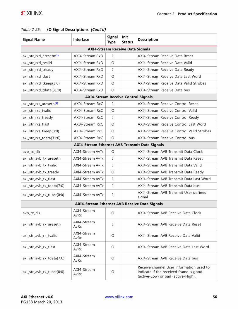
AXI Ethernet v4.0 www.xilinx.com 56PG138 March 20, 2013
Chapter 2: Product Specification
AXI4-Stream Receive Data Signals
axi_str_rxd_aresetn(1) AXI4-Stream RxD I AXI4-Stream Receive Data Reset
axi_str_rxd_tvalid AXI4-Stream RxD O AXI4-Stream Receive Data Valid
axi_str_rxd_tready AXI4-Stream RxD I AXI4-Stream Receive Data Ready
axi_str_rxd_tlast AXI4-Stream RxD O AXI4-Stream Receive Data Last Word
axi_str_rxd_tkeep(3:0) AXI4-Stream RxD O AXI4-Stream Receive Data Valid Strobes
axi_str_rxd_tdata(31:0) AXI4-Stream RxD O AXI4-Stream Receive Data bus
AXI4-Stream Receive Control Signals
axi_str_rxs_aresetn(1) AXI4-Stream RxC I AXI4-Stream Receive Control Reset
axi_str_rxs_tvalid AXI4-Stream RxC O AXI4-Stream Receive Control Valid
axi_str_rxs_tready AXI4-Stream RxC I AXI4-Stream Receive Control Ready
axi_str_rxs_tlast AXI4-Stream RxC O AXI4-Stream Receive Control Last Word
axi_str_rxs_tkeep(3:0) AXI4-Stream RxC O AXI4-Stream Receive Control Valid Strobes
axi_str_rxs_tdata(31:0) AXI4-Stream RxC O AXI4-Stream Receive Control bus
AXI4-Stream Ethernet AVB Transmit Data Signals
avb_tx_clk AXI4-Stream AvTx O AXI4-Stream AVB Transmit Data Clock
axi_str_avb_tx_aresetn AXI4-Stream AvTx I AXI4-Stream AVB Transmit Data Reset
axi_str_avb_tx_tvalid AXI4-Stream AvTx I AXI4-Stream AVB Transmit Data Valid
axi_str_avb_tx_tready AXI4-Stream AvTx O AXI4-Stream AVB Transmit Data Ready
axi_str_avb_tx_tlast AXI4-Stream AvTx I AXI4-Stream AVB Transmit Data Last Word
axi_str_avb_tx_tdata(7:0) AXI4-Stream AvTx I AXI4-Stream AVB Transmit Data bus
axi_str_avb_tx_tuser(0:0) AXI4-Stream AvTx I AXI4-Stream AVB Transmit User defined signal
AXI4-Stream Ethernet AVB Receive Data Signals
avb_rx_clk AXI4-Stream AvRx O AXI4-Stream AVB Receive Data Clock
axi_str_avb_rx_aresetn AXI4-Stream AvRx I AXI4-Stream AVB Receive Data Reset
axi_str_avb_rx_tvalid AXI4-Stream AvRx O AXI4-Stream AVB Receive Data Valid
axi_str_avb_rx_tlast AXI4-Stream AvRx O AXI4-Stream AVB Receive Data Last Word
axi_str_avb_rx_tdata(7:0) AXI4-Stream AvRx O AXI4-Stream AVB Receive Data bus
axi_str_avb_rx_tuser(0:0) AXI4-Stream AvRx O
Receive channel User information used to indicate if the received frame is good (active-Low) or bad (active-High).
Table 2‐25: I/O Signal Descriptions (Cont’d)
Signal Name InterfaceSignalType
InitStatus
Description
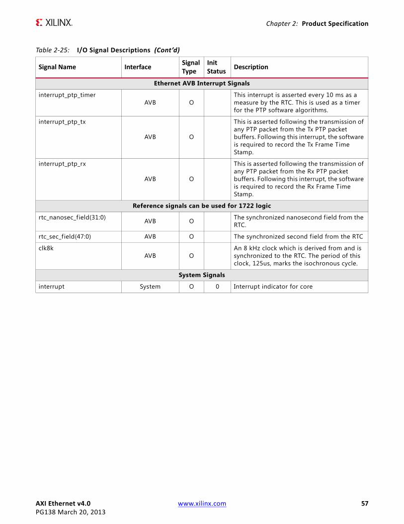
AXI Ethernet v4.0 www.xilinx.com 57PG138 March 20, 2013
Chapter 2: Product Specification
Ethernet AVB Interrupt Signals
interrupt_ptp_timerAVB O
This interrupt is asserted every 10 ms as a measure by the RTC. This is used as a timer for the PTP software algorithms.
interrupt_ptp_tx
AVB O
This is asserted following the transmission of any PTP packet from the Tx PTP packet buffers. Following this interrupt, the software is required to record the Tx Frame Time Stamp.
interrupt_ptp_rx
AVB O
This is asserted following the transmission of any PTP packet from the Rx PTP packet buffers. Following this interrupt, the software is required to record the Rx Frame Time Stamp.
Reference signals can be used for 1722 logic
rtc_nanosec_field(31:0) AVB O The synchronized nanosecond f ield from the RTC.
rtc_sec_field(47:0) AVB O The synchronized second f ield from the RTC
clk8kAVB O
An 8 kHz clock which is derived from and is synchronized to the RTC. The period of this clock, 125us, marks the isochronous cycle.
System Signals
interrupt System O 0 Interrupt indicator for core
Table 2‐25: I/O Signal Descriptions (Cont’d)
Signal Name InterfaceSignalType
InitStatus
Description
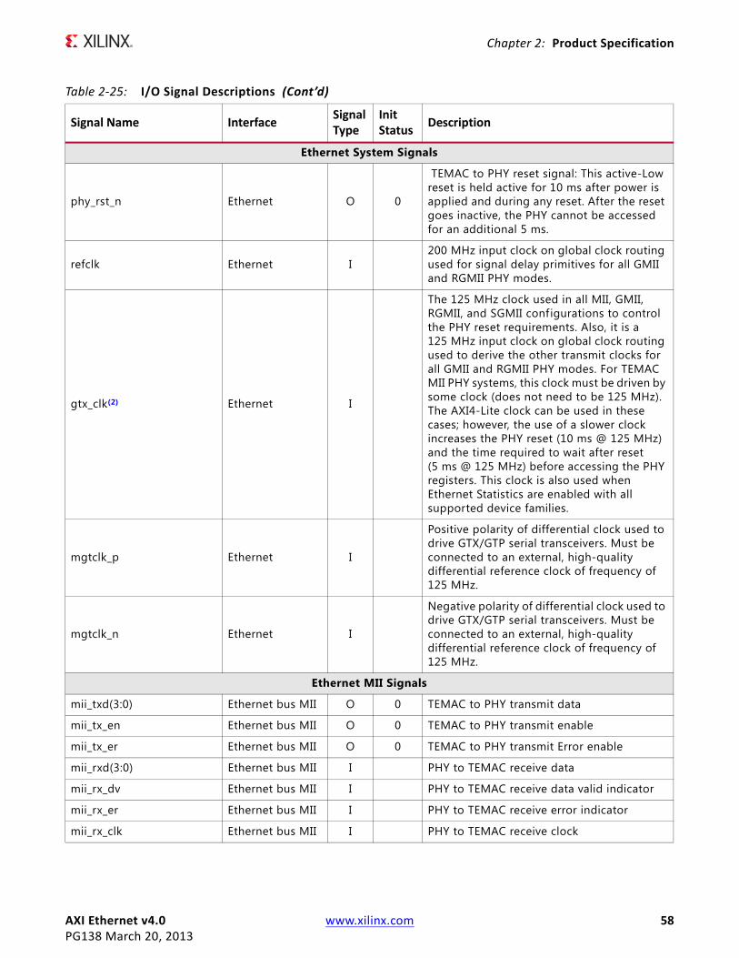
AXI Ethernet v4.0 www.xilinx.com 58PG138 March 20, 2013
Chapter 2: Product Specification
Ethernet System Signals
phy_rst_n Ethernet O 0
TEMAC to PHY reset signal: This active-Low reset is held active for 10 ms after power is applied and during any reset. After the reset goes inactive, the PHY cannot be accessed for an additional 5 ms.
refclk Ethernet I200 MHz input clock on global clock routing used for signal delay primitives for all GMII and RGMII PHY modes.
gtx_clk(2) Ethernet I
The 125 MHz clock used in all MII, GMII, RGMII, and SGMII configurations to control the PHY reset requirements. Also, it is a 125 MHz input clock on global clock routing used to derive the other transmit clocks for all GMII and RGMII PHY modes. For TEMAC MII PHY systems, this clock must be driven by some clock (does not need to be 125 MHz). The AXI4-Lite clock can be used in these cases; however, the use of a slower clock increases the PHY reset (10 ms @ 125 MHz) and the time required to wait after reset (5 ms @ 125 MHz) before accessing the PHY registers. This clock is also used when Ethernet Statistics are enabled with all supported device families.
mgtclk_p Ethernet I
Positive polarity of differential clock used to drive GTX/GTP serial transceivers. Must be connected to an external, high-quality differential reference clock of frequency of 125 MHz.
mgtclk_n Ethernet I
Negative polarity of differential clock used to drive GTX/GTP serial transceivers. Must be connected to an external, high-quality differential reference clock of frequency of 125 MHz.
Ethernet MII Signals
mii_txd(3:0) Ethernet bus MII O 0 TEMAC to PHY transmit data
mii_tx_en Ethernet bus MII O 0 TEMAC to PHY transmit enable
mii_tx_er Ethernet bus MII O 0 TEMAC to PHY transmit Error enable
mii_rxd(3:0) Ethernet bus MII I PHY to TEMAC receive data
mii_rx_dv Ethernet bus MII I PHY to TEMAC receive data valid indicator
mii_rx_er Ethernet bus MII I PHY to TEMAC receive error indicator
mii_rx_clk Ethernet bus MII I PHY to TEMAC receive clock
Table 2‐25: I/O Signal Descriptions (Cont’d)
Signal Name InterfaceSignalType
InitStatus
Description

AXI Ethernet v4.0 www.xilinx.com 59PG138 March 20, 2013
Chapter 2: Product Specification
mii_tx_clk(2) Ethernet bus MII I PHY to TEMAC transmit clock (also used for GMII/MII mode)
Ethernet GMII Signals
gmii_txd(7:0) Ethernet bus GMII O 0 TEMAC to PHY transmit data
gmii_tx_en Ethernet bus GMII O 0 TEMAC to PHY transmit enable
gmii_tx_er Ethernet bus GMII O 0 TEMAC to PHY transmit Error enable
gmii_gtx_clk Ethernet bus GMII O 0 TEMAC to PHY transmit clock
gmii_rxd(7:0) Ethernet bus GMII I PHY to TEMAC receive data
gmii_rx_dv Ethernet bus GMII I PHY to TEMAC receive data valid indicator
gmii_rx_er Ethernet bus GMII I PHY to TEMAC receive error indicator
gmii_rx_clk Ethernet bus GMII I PHY to TEMAC receive clock
gmii_tx_clk Ethernet bus GMII I - PHY to TEMAC tx input clock in 10 and 100
Mb/s modes.
Ethernet SGMII and 1000Base-X Signals
txpEthernet bus SGMIIand 1000Base-X
O 0 TEMAC to PHY transmit data positive
txnEthernet bus SGMIIand 1000Base-X
O 0 TEMAC to PHY transmit data negative
rxpEthernet bus SGMIIand 1000Base-X
I PHY to TEMAC receive data positive
rxnEthernet bus SGMIIand 1000Base-X
I PHY to TEMAC receive data negative
Ethernet RGMII Signals
rgmii_txd(3:0) Ethernet bus RGMII O 0 TEMAC to PHY transmit data
rgmii_tx_ctl Ethernet bus RGMII O 0 TEMAC to PHY transmit control
rgmii_txc Ethernet bus RGMII O 0 TEMAC to PHY transmit clock
Table 2‐25: I/O Signal Descriptions (Cont’d)
Signal Name InterfaceSignalType
InitStatus
Description

AXI Ethernet v4.0 www.xilinx.com 60PG138 March 20, 2013
Chapter 2: Product Specification
AXI4‐Stream Interface
The Ethernet frame data to be transmitted and the frame data that is received passes between the AXI Ethernet core and the rest of the embedded system through AXI4-Stream interfaces. In many cases the other end of the AXI4-Stream interfaces are connected to a soft IP DMA controller implemented in FPGA logic. However, any custom logic can be used to connect to the AXI4-Stream interface as long as it meets the requirements of the AXI Ethernet core AXI4-Stream interface.
The AXI4-Stream interface is a high-performance, synchronous, point-to-point connection which, in its general use case, is described in its specif ication listed in the References in Appendix C. This section describes the specif ic 32-bit implementation used by the AXI Ethernet core to transfer transmit and receive Ethernet frame data with the rest of the embedded system. The AXI4-Stream model used is called Packetized and Aligned Strobe which is defined in the subsequent sections.
Packetized
Data is transferred in packets rather than as a continuous stream. The signals *_TLAST are used to indicate the last 32-bit word of a packet being transferred.
rgmii_rxd(3:0) Ethernet bus RGMII I PHY to TEMAC receive data
rgmii_rx_ctl Ethernet bus RGMII I PHY to TEMAC receive control
rgmii_rxc Ethernet bus RGMII I PHY to TEMAC receive clock
Ethernet MII Management Interface (MIIM) Signals
mdc Ethernet bus MIIM O 0 TEMAC to PHY MII management bus clock
mdio(4) Ethernet bus MIIM I/O 1 Tri-stateable bidirectional MII Management
data bus.
Notes: 1. See Resets in Chapter 3. 2. See Clocking in Chapter 3.3. This core does not support half duplex operation.4. The MDIO signal is required to be pulled High as per the PHY data sheet. If the MDIO interface is not used with the soft PCS
PMA core (C_TYPE = 1 and C_PHY_TYPE = 4 or 5), the internal MDIO_I signal must be tied High to allow MDIO communication to the internal MAC. In SGMII and 1000BaseX modes, individual mdio_i (input) mdio_o (output) and mdio_t (3-state enable) signals are provided instead of the mdio bidirectional port.
Table 2‐25: I/O Signal Descriptions (Cont’d)
Signal Name InterfaceSignalType
InitStatus
Description
AXI Ethernet v4.0 www.xilinx.com 61PG138 March 20, 2013
Chapter 2: Product Specification
Aligned Strobe
A write strobe is used for each byte (*_TKEEP(3:0)) in the data bus (4 write strobes in our case). Null strobes are not allowed at the beginning, in the middle of a transfer, or at the end of a transfer. This means that the f irst word transferred and every additional word up until the last must contain a valid 32-bit value. The last word might be sparse which means it might contain 4, 3, 2, or 1 valid bytes aligned to the right and the write strobes are used to indicate which bytes are valid. *_TLAST is used to indicated the last data of a frame. In some cases the write strobe signals can be tied to the active state (1) (see Transmit AXI4-Stream Interface).
Throttling
The driver of the AXI4-Stream uses the *_TVALID to throttle during a transfer. By taking *_TVALID inactive the current transfer is held until it is active again. The receiver of the AXI4-Stream uses the *_TREADY signal to throttle during a transfer. By taking *_TREADY inactive the current transfer is held until it is active again.
Dual Channel AXI4‐Stream
The transmit AXI4-Stream interface uses two AXI4-Stream buses. The AXI4-Stream Data Bus is used for frame data only while the AXI4-Stream Control Bus contains control information. Similarly, the receive AXI4-Stream interface uses two AXI4-Stream buses. The AXI4-Stream Data Bus is used for frame data only, and the AXI4-Stream Status Bus provides status information. The control/status and data buses must have the same clock source but there is no synchronization between the two buses with regards to frame to frame data.
The transmit AXI4-Stream control bus can be configured to use one of two format types: Normal Transmit or Receive Status Transmit. This configuration is controlled by the f irst nibble (4-bits aligned left) of the f irst word transferred on the transmit control bus and the receive status bus. A value of 0xA identif ies the transfer as a Normal Transmit control packet. A value of 0x5 identif ies the transfer as a Receive Status packet. All other values are currently undefined and are ignored. These transfer types are defined in Normal Transmit AXI4-Stream Transfer - Flag=0xA and Receive Status Transmit AXI4-Stream Transfer - Flag=0x5. The receive AXI4-Stream interface only supports one format type.
Functional Description
The AXI4-Stream interface transfers data in one direction only. The Ethernet transmit interface uses an AXI4-Stream Data interface and an AXI4-Stream Control interface. The Ethernet receive interface uses an AXI4-Stream Data interface and an AXI4-Stream Status interface. The AXI4-Stream interfaces used in this implementation are 32-bits wide, have side-band control signals, and typically operate with a clock between 100 and 125 MHz. Data is transferred across the AXI4-Stream Data interfaces. Additional control information is transferred across the transmit AXI4-Stream Control interface and additional status information is transferred across the receive AXI4-Stream Status interface.
AXI Ethernet v4.0 www.xilinx.com 62PG138 March 20, 2013
Chapter 2: Product Specification
For the transmit datapath the Source is the embedded system, typically a DMA controller, and the Destination is the AXI Ethernet core. For the receive datapath the Source is the AXI Ethernet and the Destination is the embedded system, typically a DMA controller.
Control signals are used to mark the start and end of data across the AXI4-Stream interfaces as well as to signal the readiness of the Source and Destination and to indicate which bytes in the 32-bit path contain valid data. The destination uses the *_TREADY signal to indicate it is able to receive data, while the source uses *_TVALID to indicated when valid data is on the bus and the *_TLAST signal to indicate the last 8, 16, 24, or 32 bits of data.
Transmit AXI4‐Stream Interface
The transmit control block must maintain coherence between the data and control buses. Because data frames can vary from 1 byte to over 9 kb in length and the control information for each frame is a constant, six 32-bit words, care must be taken under conditions where the buffer for the frame data or control data fills up to prevent an out of sequence condition to occur.
To maintain coherency, the AXI4-Stream data ready signal is held not ready until a AXI4-Stream control stream has been received. After this has occurred, the AXI4-Stream data ready signal is driven ready (as long as there is buffer space available) and the AXI4-Stream control ready signal is held not ready until the data stream transfer is complete (Figure 2-21 and Figure 2-23). The write strobe signals for the control and status buses are always in the active state (0xF). Also, the right-most write strobe signal for the data bus is always in the active state (0x1, 0x3, 0x7, or 0xF). These signals can be tied off rather than routing signals from the AXI4-Stream source to the destination. The AXI Ethernet core provides these ports to be compliant with the standard; however, there is not any logic based on these inputs which are considered constants. The transmit interface can encounter two AXI4-Stream transfer types: Normal Transmit or Receive Status Transmit.
Normal Transmit AXI4‐Stream Transfer ‐ Flag=0xA
The Normal Transmit transfer is used to connect the AXI Ethernet core to an external core.
Figure 2-21 illustrates the waveforms when connected to a core such as AXI_DMA or AXI_FIFO_MM_S. AXI_DMA supports advanced features such as partial CSUM offloading or extended VLAN; however, AXI_FIFO_MM_S does not support any of the advanced features.
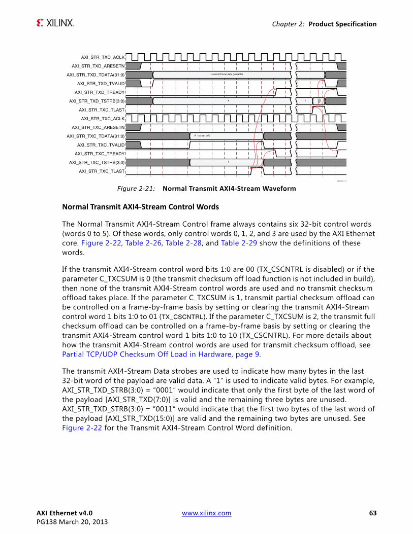
AXI Ethernet v4.0 www.xilinx.com 63PG138 March 20, 2013
Chapter 2: Product Specification
Normal Transmit AXI4‐Stream Control Words
The Normal Transmit AXI4-Stream Control frame always contains six 32-bit control words (words 0 to 5). Of these words, only control words 0, 1, 2, and 3 are used by the AXI Ethernet core. Figure 2-22, Table 2-26, Table 2-28, and Table 2-29 show the definitions of these words.
If the transmit AXI4-Stream control word bits 1:0 are 00 (TX_CSCNTRL is disabled) or if the parameter C_TXCSUM is 0 (the transmit checksum off load function is not included in build), then none of the transmit AXI4-Stream control words are used and no transmit checksum offload takes place. If the parameter C_TXCSUM is 1, transmit partial checksum offload can be controlled on a frame-by-frame basis by setting or clearing the transmit AXI4-Stream control word 1 bits 1:0 to 01 (TX_CSCNTRL). If the parameter C_TXCSUM is 2, the transmit full checksum offload can be controlled on a frame-by-frame basis by setting or clearing the transmit AXI4-Stream control word 1 bits 1:0 to 10 (TX_CSCNTRL). For more details about how the transmit AXI4-Stream control words are used for transmit checksum offload, see Partial TCP/UDP Checksum Off Load in Hardware, page 9.
The transmit AXI4-Stream Data strobes are used to indicate how many bytes in the last 32-bit word of the payload are valid data. A “1” is used to indicate valid bytes. For example, AXI_STR_TXD_STRB(3:0) = “0001” would indicate that only the f irst byte of the last word of the payload [AXI_STR_TXD(7:0)] is valid and the remaining three bytes are unused. AXI_STR_TXD_STRB(3:0) = “0011” would indicate that the f irst two bytes of the last word of the payload [AXI_STR_TXD(15:0)] are valid and the remaining two bytes are unused. See Figure 2-22 for the Transmit AXI4-Stream Control Word definition.
X-Ref Target - Figure 2-21
Figure 2‐21: Normal Transmit AXI4‐Stream Waveform
AXI_STR_TXD_ACLK
AXI_STR_TXD_ARESETN
AXI_STR_TXD_TDATA(31:0)
AXI_STR_TXD_TVALID
AXI_STR_TXD_TREADY
AXI_STR_TXD_TSTRB(3:0)
AXI_STR_TXD_TLAST
AXI_STR_TXC_ACLK
AXI_STR_TXC_ARESETN
AXI_STR_TXC_TDATA(31:0)
AXI_STR_TXC_TVALID
AXI_STR_TXC_TREADY
AXI_STR_TXC_TSTRB(3:0)
AXI_STR_TXC_TLAST
DS759 57
A tx cntrl info
transmit frame data (variable)
F F
F
1,3,7,F

AXI Ethernet v4.0 www.xilinx.com 64PG138 March 20, 2013
Chapter 2: Product Specification
X-Ref Target - Figure 2-22
Figure 2‐22: Transmit AXI4‐Stream Control Words
MS
B
LSB
31 Word 0
Word 2
TxCsInit 0 15 16 31 reserved for future use
TxCsInsert 0 15 16 31 TxCsBegin
0 31
0 31
Word 3
Word 4
Word 5
Transmit AXI4-Stream Control Words
2728flag = A reserved for future use
reserved for future use
reserved for future use
0
1231 Word 1reserved for future use 0
TxCsCntrl
DS759_58
Table 2‐26: Transmit AXI4‐Stream Control Word 0 ‐ TAG
Bits Name Description
31-28 Flag1010 = Normal Transmit Frame0101= Receive Status Transmit FrameAll other selections are reserved.
27-0 Reserved Reserved for future use
Table 2‐27: Transmit AXI4‐Stream Control Word 1‐ APP0
Bits Name Description
31-2 Reserved Reserved for future use
1-0 TxCsumCntrl
Transmit Checksum Enable:• 00 = No transmit checksum offloading should be performed on this frame• 01 = Partial transmit checksum offloading should be performed on this frame based
upon other data provided in the control words. For the partial checksum to be performed, C_TXCSUM must be set to 1.
• 10 = Full transmit IP and TCP/UDP checksum offloading should be performed on this frame if it meets the requirements. For the full checksum to performed, C_TXCSUM must be set to 2.
• 11 = Reserved
Table 2‐28: Transmit AXI4‐Stream Control Word 2‐ APP1
Bits Name Description
31-16 TxCsBeginTransmit Checksum Calculation Starting Point: This value is the offset to the location in the frame to the f irst byte that needs to be included in the checksum calculation. The f irst byte is indicated by a value of zero. The beginning position must be 16-bit aligned.
15-0 TxCsInsert
Transmit Checksum Insertion Point: This value is the offset to the location in the frame where the checksum value should be written into the TCP or UDP segment header. The value must be 16-bit aligned and cannot be in the first 8 bytes of the frame. It also should not contain a value that exceeds the length of the frame.

AXI Ethernet v4.0 www.xilinx.com 65PG138 March 20, 2013
Chapter 2: Product Specification
Receive Status Transmit AXI4‐Stream Transfer ‐ Flag=0x5
The Receive Status transfer is utilized when the receive AXI4-Stream interface is tied directly to the transmit AXI4-Stream interface for the purpose of looping back Ethernet receive data to the Ethernet transmit interface with no external intervention. In that case the status transfer enables the receive data frame to be presented to the TEMAC transmitter and the status content is ignored. No advanced checksum offload or VLAN functions is allowed for these operations even if they were included in the core at build time. Notice the different identif ication flag value in Figure 2-23.
Receive AXI4‐Stream Interface
Unlike the transmit AXI4-Stream Control interface, the receive AXI4-Stream Status interface has only one format type (TAG/FLAG).
The receive interface has been designed to allow throttling on both the AXI4-Stream Status bus and the AXI4-Stream Data bus. After receiving Ethernet data, the receive interface transfers the AXI4-Stream Status information before the AXI4-Stream Data information. See Figure 2-26 for a receive waveform diagram. This diagram shows what signals are required when connected to a core such as AXI_DMA. When connecting to a core such as AXI_FIFO_MM_S, a signal minimization can be made because the receive status bus information is not required.
Table 2‐29: Transmit AXI4‐Stream Control Word 3‐ APP2
Bits Name Description
31-16 Reserved Undefined value.
15-0 TxCsInitTransmit Checksum Calculation Initial Value: This value is a 16-bit seed that can be used to insert the TCP or UDP pseudo header into the checksum calculation. See Partial TCP/UDP Checksum Off Load in Hardware, page 9 for more information on using this field.
X-Ref Target - Figure 2-23
Figure 2‐23: Receive Status Transmit AXI4‐Stream Waveform
AXI_STR_TXD_ACLK
AXI_STR_TXD_ARESETN
AXI_STR_TXD_TDATA(31:0)
AXI_STR_TXD_TVALID
AXI_STR_TXD_TREADY
AXI_STR_TXD_TSTRB(3:0)
AXI_STR_TXD_TLAST
AXI_STR_TXC_ACLK
AXI_STR_TXC_ARESETN
AXI_STR_TXC_TDATA(31:0)
AXI_STR_TXC_TVALID
AXI_STR_TXC_TREADY
AXI_STR_TXC_TSTRB(3:0)
AXI_STR_TXC_TLAST
DS759_59
5 tx cntrl info
transmit frame data (variable)
F F
F
1,3,7,F
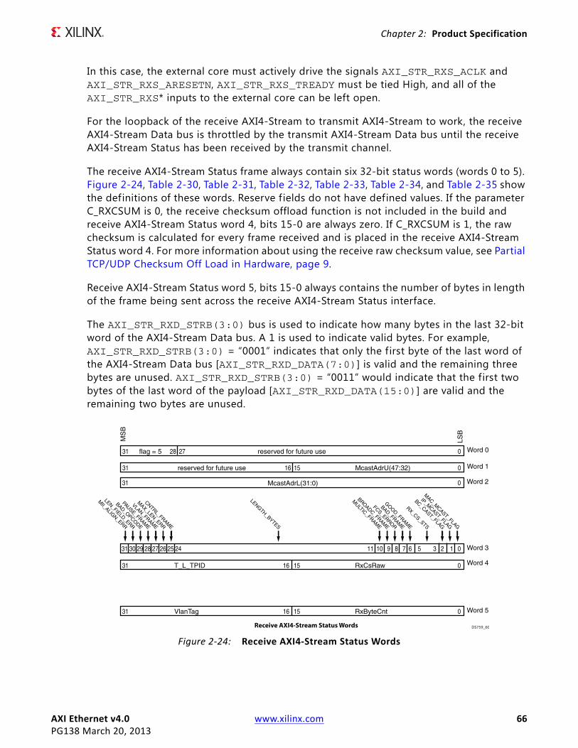
AXI Ethernet v4.0 www.xilinx.com 66PG138 March 20, 2013
Chapter 2: Product Specification
In this case, the external core must actively drive the signals AXI_STR_RXS_ACLK and AXI_STR_RXS_ARESETN, AXI_STR_RXS_TREADY must be tied High, and all of the AXI_STR_RXS* inputs to the external core can be left open.
For the loopback of the receive AXI4-Stream to transmit AXI4-Stream to work, the receive AXI4-Stream Data bus is throttled by the transmit AXI4-Stream Data bus until the receive AXI4-Stream Status has been received by the transmit channel.
The receive AXI4-Stream Status frame always contain six 32-bit status words (words 0 to 5). Figure 2-24, Table 2-30, Table 2-31, Table 2-32, Table 2-33, Table 2-34, and Table 2-35 show the definitions of these words. Reserve f ields do not have defined values. If the parameter C_RXCSUM is 0, the receive checksum offload function is not included in the build and receive AXI4-Stream Status word 4, bits 15-0 are always zero. If C_RXCSUM is 1, the raw checksum is calculated for every frame received and is placed in the receive AXI4-Stream Status word 4. For more information about using the receive raw checksum value, see Partial TCP/UDP Checksum Off Load in Hardware, page 9.
Receive AXI4-Stream Status word 5, bits 15-0 always contains the number of bytes in length of the frame being sent across the receive AXI4-Stream Status interface.
The AXI_STR_RXD_STRB(3:0) bus is used to indicate how many bytes in the last 32-bit word of the AXI4-Stream Data bus. A 1 is used to indicate valid bytes. For example, AXI_STR_RXD_STRB(3:0) = “0001” indicates that only the f irst byte of the last word of the AXI4-Stream Data bus [AXI_STR_RXD_DATA(7:0)] is valid and the remaining three bytes are unused. AXI_STR_RXD_STRB(3:0) = “0011” would indicate that the first two bytes of the last word of the payload [AXI_STR_RXD_DATA(15:0)] are valid and the remaining two bytes are unused.
X-Ref Target - Figure 2-24ds759_49.epsds759_49.eps
Figure 2‐24: Receive AXI4‐Stream Status Words
MS
B
LSB
Word 0
Word 2
31
16
16
31
31
31
31 28 27
15
15
123567891011
0
0
0
0
0
30 29 28 27 26 25 24
McastAdrL(31:0)
Word 3
Word 4
Word 5
Receive AXI4-Stream Status Words
flag = 5
MAC_M
CAST_FLAG
IP_MCAST_FLAG
BC_CAST_FLAG
RX_CS_STS
BAD_OPCODE
LEN_FIELD_ERR
MII_ALIGN_ERR
MAX_LEN_ERR
VLAN_FRAME
PAUSE_FRAME
LENGTH_BYTES
CNTRL_FRAME
GOOD_FRAME
BAD_FRAME
FCS_ERROR
BROADC_FRAME
MULTIC_FRAM
E
reserved for future use
Word 11631 15 0McastAdrU(47:32)reserved for future use
RxCsRawT_L_TPID
RxByteCntVlanTag
DS759_60
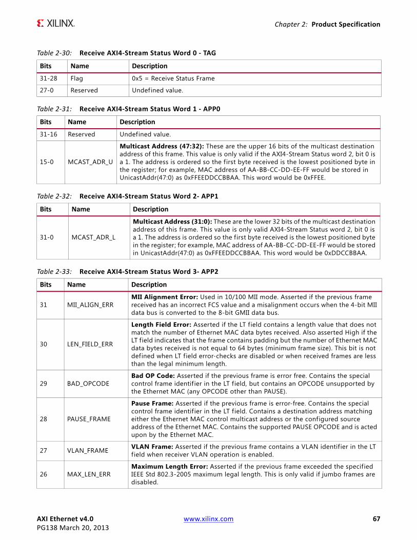
AXI Ethernet v4.0 www.xilinx.com 67PG138 March 20, 2013
Chapter 2: Product Specification
Table 2‐30: Receive AXI4‐Stream Status Word 0 ‐ TAG
Bits Name Description
31-28 Flag 0x5 = Receive Status Frame
27-0 Reserved Undefined value.
Table 2‐31: Receive AXI4‐Stream Status Word 1 ‐ APP0
Bits Name Description
31-16 Reserved Undefined value.
15-0 MCAST_ADR_U
Multicast Address (47:32): These are the upper 16 bits of the multicast destination address of this frame. This value is only valid if the AXI4-Stream Status word 2, bit 0 is a 1. The address is ordered so the f irst byte received is the lowest positioned byte in the register; for example, MAC address of AA-BB-CC-DD-EE-FF would be stored in UnicastAddr(47:0) as 0xFFEEDDCCBBAA. This word would be 0xFFEE.
Table 2‐32: Receive AXI4‐Stream Status Word 2‐ APP1
Bits Name Description
31-0 MCAST_ADR_L
Multicast Address (31:0): These are the lower 32 bits of the multicast destination address of this frame. This value is only valid AXI4-Stream Status word 2, bit 0 is a 1. The address is ordered so the first byte received is the lowest positioned byte in the register; for example, MAC address of AA-BB-CC-DD-EE-FF would be stored in UnicastAddr(47:0) as 0xFFEEDDCCBBAA. This word would be 0xDDCCBBAA.
Table 2‐33: Receive AXI4‐Stream Status Word 3‐ APP2
Bits Name Description
31 MII_ALIGN_ERRMII Alignment Error: Used in 10/100 MII mode. Asserted if the previous frame received has an incorrect FCS value and a misalignment occurs when the 4-bit MII data bus is converted to the 8-bit GMII data bus.
30 LEN_FIELD_ERR
Length Field Error: Asserted if the LT f ield contains a length value that does not match the number of Ethernet MAC data bytes received. Also asserted High if the LT field indicates that the frame contains padding but the number of Ethernet MAC data bytes received is not equal to 64 bytes (minimum frame size). This bit is not defined when LT field error-checks are disabled or when received frames are less than the legal minimum length.
29 BAD_OPCODEBad OP Code: Asserted if the previous frame is error free. Contains the special control frame identif ier in the LT f ield, but contains an OPCODE unsupported by the Ethernet MAC (any OPCODE other than PAUSE).
28 PAUSE_FRAME
Pause Frame: Asserted if the previous frame is error-free. Contains the special control frame identif ier in the LT f ield. Contains a destination address matching either the Ethernet MAC control multicast address or the configured source address of the Ethernet MAC. Contains the supported PAUSE OPCODE and is acted upon by the Ethernet MAC.
27 VLAN_FRAME VLAN Frame: Asserted if the previous frame contains a VLAN identif ier in the LT f ield when receiver VLAN operation is enabled.
26 MAX_LEN_ERRMaximum Length Error: Asserted if the previous frame exceeded the specified IEEE Std 802.3-2005 maximum legal length. This is only valid if jumbo frames are disabled.
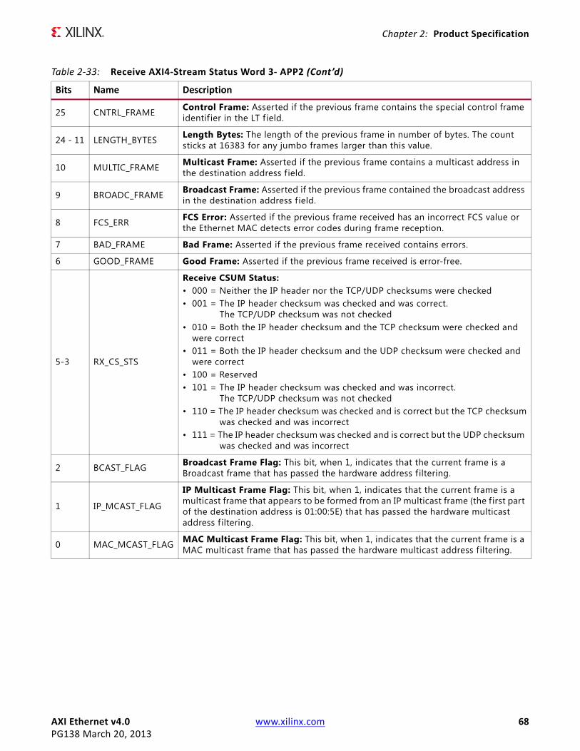
AXI Ethernet v4.0 www.xilinx.com 68PG138 March 20, 2013
Chapter 2: Product Specification
25 CNTRL_FRAME Control Frame: Asserted if the previous frame contains the special control frame identif ier in the LT f ield.
24 - 11 LENGTH_BYTES Length Bytes: The length of the previous frame in number of bytes. The count sticks at 16383 for any jumbo frames larger than this value.
10 MULTIC_FRAME Multicast Frame: Asserted if the previous frame contains a multicast address in the destination address f ield.
9 BROADC_FRAME Broadcast Frame: Asserted if the previous frame contained the broadcast address in the destination address field.
8 FCS_ERR FCS Error: Asserted if the previous frame received has an incorrect FCS value or the Ethernet MAC detects error codes during frame reception.
7 BAD_FRAME Bad Frame: Asserted if the previous frame received contains errors.
6 GOOD_FRAME Good Frame: Asserted if the previous frame received is error-free.
5-3 RX_CS_STS
Receive CSUM Status: • 000 = Neither the IP header nor the TCP/UDP checksums were checked• 001 = The IP header checksum was checked and was correct.
The TCP/UDP checksum was not checked• 010 = Both the IP header checksum and the TCP checksum were checked and
were correct• 011 = Both the IP header checksum and the UDP checksum were checked and
were correct• 100 = Reserved• 101 = The IP header checksum was checked and was incorrect.
The TCP/UDP checksum was not checked• 110 = The IP header checksum was checked and is correct but the TCP checksum
was checked and was incorrect• 111 = The IP header checksum was checked and is correct but the UDP checksum
was checked and was incorrect
2 BCAST_FLAG Broadcast Frame Flag: This bit, when 1, indicates that the current frame is a Broadcast frame that has passed the hardware address f iltering.
1 IP_MCAST_FLAG
IP Multicast Frame Flag: This bit, when 1, indicates that the current frame is a multicast frame that appears to be formed from an IP multicast frame (the f irst part of the destination address is 01:00:5E) that has passed the hardware multicast address filtering.
0 MAC_MCAST_FLAG MAC Multicast Frame Flag: This bit, when 1, indicates that the current frame is a MAC multicast frame that has passed the hardware multicast address f iltering.
Table 2‐33: Receive AXI4‐Stream Status Word 3‐ APP2 (Cont’d)
Bits Name Description
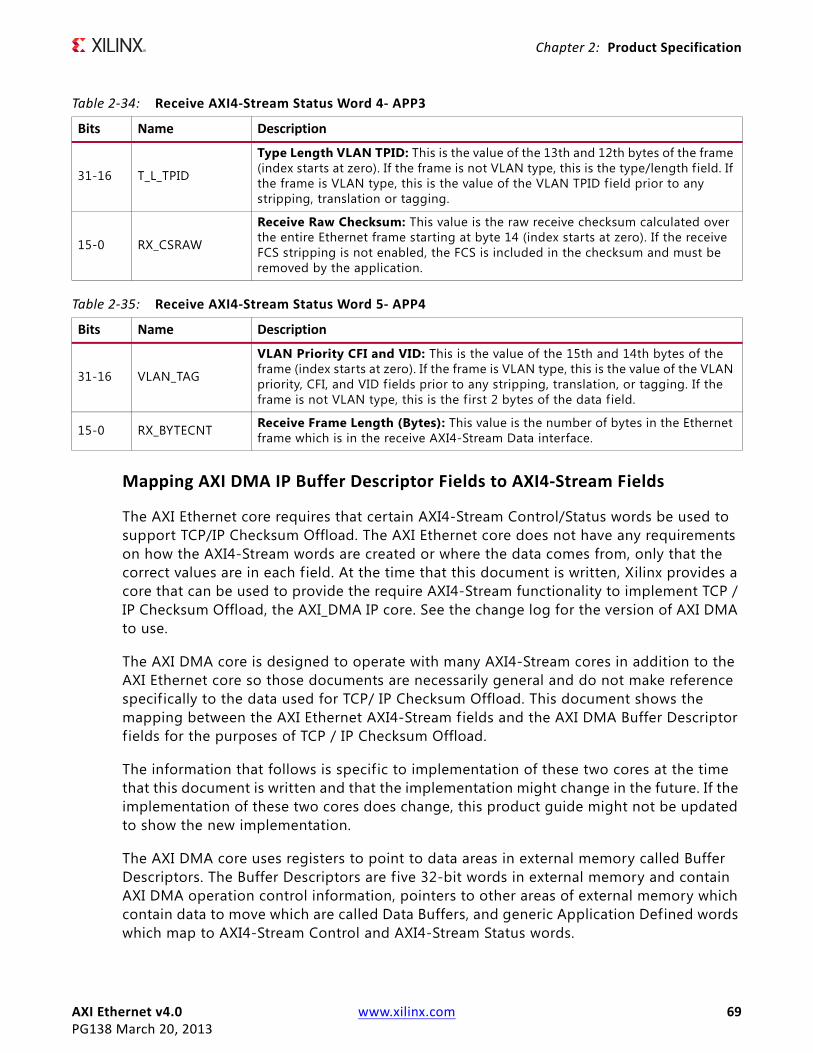
AXI Ethernet v4.0 www.xilinx.com 69PG138 March 20, 2013
Chapter 2: Product Specification
Mapping AXI DMA IP Buffer Descriptor Fields to AXI4‐Stream Fields
The AXI Ethernet core requires that certain AXI4-Stream Control/Status words be used to support TCP/IP Checksum Offload. The AXI Ethernet core does not have any requirements on how the AXI4-Stream words are created or where the data comes from, only that the correct values are in each f ield. At the time that this document is written, Xilinx provides a core that can be used to provide the require AXI4-Stream functionality to implement TCP / IP Checksum Offload, the AXI_DMA IP core. See the change log for the version of AXI DMA to use.
The AXI DMA core is designed to operate with many AXI4-Stream cores in addition to the AXI Ethernet core so those documents are necessarily general and do not make reference specifically to the data used for TCP/ IP Checksum Offload. This document shows the mapping between the AXI Ethernet AXI4-Stream fields and the AXI DMA Buffer Descriptor f ields for the purposes of TCP / IP Checksum Offload.
The information that follows is specific to implementation of these two cores at the time that this document is written and that the implementation might change in the future. If the implementation of these two cores does change, this product guide might not be updated to show the new implementation.
The AXI DMA core uses registers to point to data areas in external memory called Buffer Descriptors. The Buffer Descriptors are five 32-bit words in external memory and contain AXI DMA operation control information, pointers to other areas of external memory which contain data to move which are called Data Buffers, and generic Application Defined words which map to AXI4-Stream Control and AXI4-Stream Status words.
Table 2‐34: Receive AXI4‐Stream Status Word 4‐ APP3
Bits Name Description
31-16 T_L_TPID
Type Length VLAN TPID: This is the value of the 13th and 12th bytes of the frame (index starts at zero). If the frame is not VLAN type, this is the type/length f ield. If the frame is VLAN type, this is the value of the VLAN TPID f ield prior to any stripping, translation or tagging.
15-0 RX_CSRAW
Receive Raw Checksum: This value is the raw receive checksum calculated over the entire Ethernet frame starting at byte 14 (index starts at zero). If the receive FCS stripping is not enabled, the FCS is included in the checksum and must be removed by the application.
Table 2‐35: Receive AXI4‐Stream Status Word 5‐ APP4
Bits Name Description
31-16 VLAN_TAG
VLAN Priority CFI and VID: This is the value of the 15th and 14th bytes of the frame (index starts at zero). If the frame is VLAN type, this is the value of the VLAN priority, CFI, and VID f ields prior to any stripping, translation, or tagging. If the frame is not VLAN type, this is the first 2 bytes of the data field.
15-0 RX_BYTECNT Receive Frame Length (Bytes): This value is the number of bytes in the Ethernet frame which is in the receive AXI4-Stream Data interface.
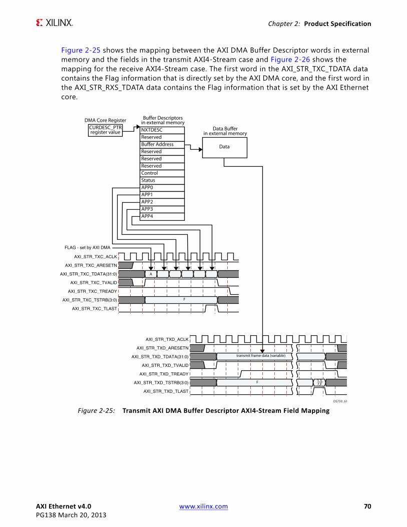
AXI Ethernet v4.0 www.xilinx.com 70PG138 March 20, 2013
Chapter 2: Product Specification
Figure 2-25 shows the mapping between the AXI DMA Buffer Descriptor words in external memory and the f ields in the transmit AXI4-Stream case and Figure 2-26 shows the mapping for the receive AXI4-Stream case. The f irst word in the AXI_STR_TXC_TDATA data contains the Flag information that is directly set by the AXI DMA core, and the f irst word in the AXI_STR_RXS_TDATA data contains the Flag information that is set by the AXI Ethernet core.
X-Ref Target - Figure 2-25
Figure 2‐25: Transmit AXI DMA Buffer Descriptor AXI4‐Stream Field Mapping
DMA Core RegisterCURDESC_PTRregister value NXTDESC
ReservedBuffer Address
ReservedReservedControlStatus
APP1APP2APP3APP4
APP0
Buffer Descriptorsin external memory
Data
Data Bufferin external memory
Reserved
DS759_61
AXI_STR_TXD_ACLK
AXI_STR_TXD_ARESETN
AXI_STR_TXD_TDATA(31:0)
AXI_STR_TXD_TVALID
AXI_STR_TXD_TREADY
AXI_STR_TXD_TSTRB(3:0)
AXI_STR_TXD_TLAST
1,3,7,FF
transmit frame data (variable)
AXI_STR_TXC_ACLK
FLAG - set by AXI DMA
AXI_STR_TXC_ARESETN
AXI_STR_TXC_TDATA(31:0)
AXI_STR_TXC_TVALID
AXI_STR_TXC_TREADY
AXI_STR_TXC_TSTRB(3:0)
AXI_STR_TXC_TLAST
F
A
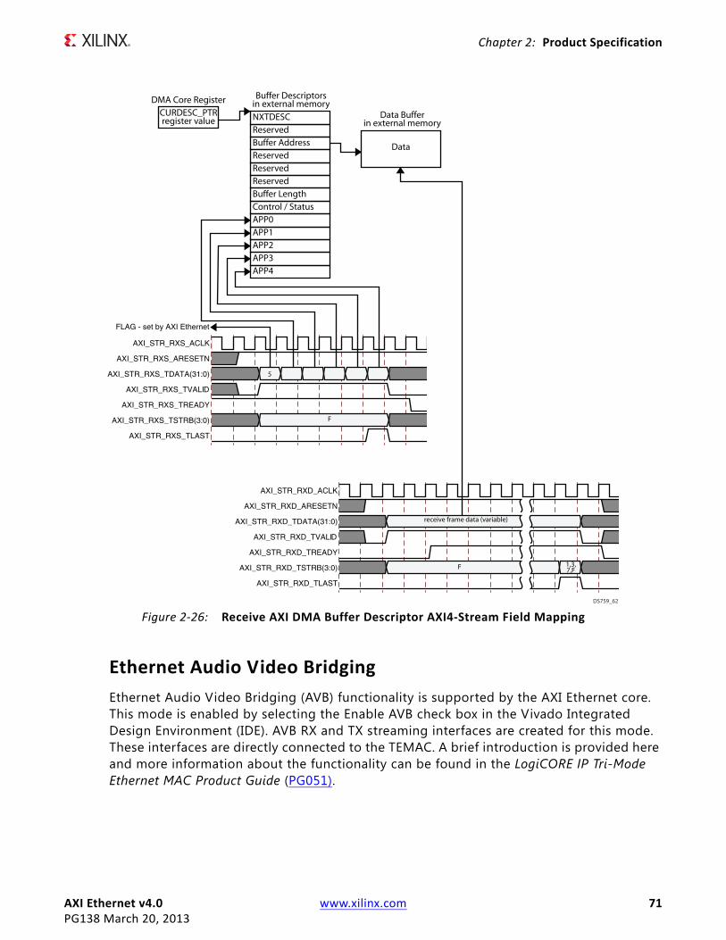
AXI Ethernet v4.0 www.xilinx.com 71PG138 March 20, 2013
Chapter 2: Product Specification
Ethernet Audio Video Bridging
Ethernet Audio Video Bridging (AVB) functionality is supported by the AXI Ethernet core. This mode is enabled by selecting the Enable AVB check box in the Vivado Integrated Design Environment (IDE). AVB RX and TX streaming interfaces are created for this mode. These interfaces are directly connected to the TEMAC. A brief introduction is provided here and more information about the functionality can be found in the LogiCORE IP Tri-Mode Ethernet MAC Product Guide (PG051).
X-Ref Target - Figure 2-26
Figure 2‐26: Receive AXI DMA Buffer Descriptor AXI4‐Stream Field Mapping
DMA Core RegisterCURDESC_PTRregister value NXTDESC
ReservedBuffer Address
ReservedReservedBuffer LengthControl / Status
APP1APP2APP3APP4
APP0
Buffer Descriptorsin external memory
Data
Data Bufferin external memory
Reserved
DS759_62
AXI_STR_RXD_ACLK
AXI_STR_RXD_ARESETN
AXI_STR_RXD_TDATA(31:0)
AXI_STR_RXD_TVALID
AXI_STR_RXD_TREADY
AXI_STR_RXD_TSTRB(3:0)
AXI_STR_RXD_TLAST
1,3,7,FF
receive frame data (variable)
AXI_STR_RXS_ACLK
FLAG - set by AXI Ethernet
AXI_STR_RXS_ARESETN
AXI_STR_RXS_TDATA(31:0)
AXI_STR_RXS_TVALID
AXI_STR_RXS_TREADY
AXI_STR_RXS_TSTRB(3:0)
AXI_STR_RXS_TLAST
F
5

AXI Ethernet v4.0 www.xilinx.com 72PG138 March 20, 2013
Chapter 2: Product Specification
AVB AXI4‐Stream Interface
The AVB AXI4-Stream interface is a limited interface in that it does not allow throttling from the external connections. As a result, some of the standard AXI4-Stream signals are missing from the port list as well as the addition of the TUSER signals. Both transmit and receive buses are 8-bits wide which eliminates the need of the write strobe signal bus. For both buses, the AXI Ethernet core provides the AXI4-Stream clocks and clock enables which are derived from the internal Ethernet clocks.
The AVB AXI4-Stream interface is connected to external logic that currently is not provided by Xilinx. Several third party partners have created this logic, have tested it with the system core, and have integrated it into AVB systems. This external logic takes time-sensitive audio or video information and splits it into Ethernet frames using a protocol encoding that is similar to TCP/IP. This is all done in FPGA logic.
Ethernet AVB frames are passed back and forth to the Ethernet through the AVB AXI4-Stream interfaces. Internal to AXI Ethernet core, the AVB frames and the legacy frames are multiplexed and demultiplexed based on a prioritization and time slotting method. The AVB function in the AXI Ethernet core is responsible for helping to choose the most accurate AVB system clock in the Ethernet network and synchronizes to the clock so all AVB nodes are synchronized.
Transmit Interface
The AXI Ethernet core provides the signal AXI_STR_AVBTX_ACLK which is derived from the TEMAC transmit MAC interface clock. This clock operates at 125 MHz when operating at 1 Gb/s and is 25 MHz when operating at 100 Mb/s. During a transfer, the AXI Ethernet core uses the TEMAC transmit MAC interface clock enable to toggle AXI_STR_AVBTX_TREADY. The clock enable is High for every clock cycle when operating at 1 Gb/s and toggles every other clock cycle for 100 Mb/s. When the AXI Ethernet core is ready to transmit an AVB frame, it drives the AXI_STR_AVBTX_TREADY signal High. When the external logic is ready to transmit a frame, it drives the AXI_STR_AVBTX_TVALID signal High and provides the f irst byte of data on the AXI_STR_AVBTX_TDATA bus. Now the external logic must provide a new byte of data on every clock cycle that the AXI_STR_AVBTX_TREADY signal is High while TVALID is active until the end of the frame is reached.
The external logic cannot throttle the AVB transmit interface. The AXI Ethernet core accepts the first byte and then drives AXI_STR_AVBTX_TREADY Low until the TEMAC has started the transmit, then it drives it back to High and continues to use it as a clock enable for the remainder of that frame.
On the last byte of the frame, the external logic drives the AXI_STR_AVBTX_TLAST signal High for one clock cycle with AXI_STR_AVBTX_TREADY. If it does not have any additional frames to transmit, it removes the TVALID signal when it takes the TLAST signal Low. However, if another frame is ready, the external logic leaves the TVALID signal High.
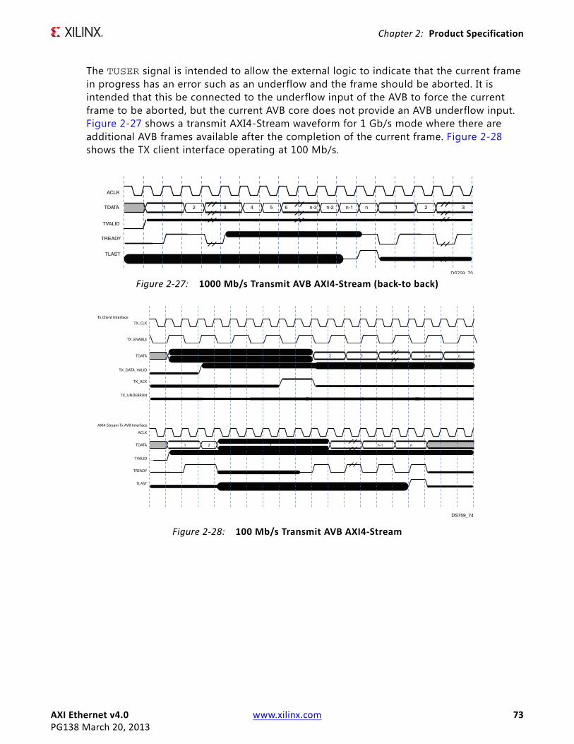
AXI Ethernet v4.0 www.xilinx.com 73PG138 March 20, 2013
Chapter 2: Product Specification
The TUSER signal is intended to allow the external logic to indicate that the current frame in progress has an error such as an underflow and the frame should be aborted. It is intended that this be connected to the underflow input of the AVB to force the current frame to be aborted, but the current AVB core does not provide an AVB underflow input. Figure 2-27 shows a transmit AXI4-Stream waveform for 1 Gb/s mode where there are additional AVB frames available after the completion of the current frame. Figure 2-28 shows the TX client interface operating at 100 Mb/s.
X-Ref Target - Figure 2-27
Figure 2‐27: 1000 Mb/s Transmit AVB AXI4‐Stream (back‐to back)
ACLK
TDATA
TVALID
TREADY
TLAST
1 2 3 1 2 34 5 6 n-3 n-2 n-1 n
DS759 73
X-Ref Target - Figure 2-28
Figure 2‐28: 100 Mb/s Transmit AVB AXI4‐Stream
ACLK
TDATA
TVALID
TREADY
TLAST
TX_CLKTx Client Interface
AXI4-Stream Tx AVB Interface
TX_ENABLE
TDATA
TX_DATA_VALID
TX_ACK
TX_UNDERRUN
1 2 3 n-1 n
n-1 n1 2 3
DS759_74
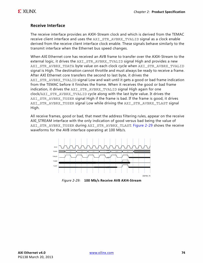
AXI Ethernet v4.0 www.xilinx.com 74PG138 March 20, 2013
Chapter 2: Product Specification
Receive Interface
The receive interface provides an AXI4-Stream clock and which is derived from the TEMAC receive client interface and uses the AXI_STR_AVBRX_TVALID signal as a clock enable derived from the receive client interface clock enable. These signals behave similarly to the transmit interface when the Ethernet bus speed changes.
When AXI Ethernet core has received an AVB frame to transfer over the AXI4-Stream to the external logic, it drives the AXI_STR_AVBRX_TVALID signal High and provides a new AXI_STR_AVBRX_TDATA byte value on each clock cycle when AXI_STR_AVBRX_TVALID signal is High. The destination cannot throttle and must always be ready to receive a frame. After AXI Ethernet core transfers the second to last byte, it drives the AXI_STR_AVBRX_TVALID signal Low and wait until it gets a good or bad frame indication from the TEMAC before it f inishes the frame. When it receives the good or bad frame indication, it drives the AXI_STR_AVBRX_TVALID signal High again for one clock/AXI_STR_AVBRX_TVALID cycle along with the last byte value. It drives the AXI_STR_AVBRX_TUSER signal High if the frame is bad. If the frame is good, it drives AXI_STR_AVBRX_TUSER signal Low while driving the AXI_STR_AVBRX_TLAST signal High.
All receive frames, good or bad, that meet the address f iltering rules, appear on the receive AXI_STREAM interface with the only indication of good versus bad being the value of AXI_STR_AVBRX_TUSER during AXI_STR_AVBRX_TLAST. Figure 2-29 shows the receive waveforms for the AVB interface operating at 100 Mb/s.
X-Ref Target - Figure 2-29
Figure 2‐29: 100 Mb/s Receive AVB AXI4‐Stream
ACLK
TDATA
TVALID
TUSER
TLAST
n-1 n1 2 3
DS759_75

AXI Ethernet v4.0 www.xilinx.com 75PG138 March 20, 2013
Chapter 2: Product Specification
Statistics Vectors
Transmit Statistics Vector
The transmitter provides 32 bits of statistics for each frame transmitted as well as a signal which can be used to count the total number of bytes transmitted. Statistics information is provided using a 32-bit vector for one clock cycle as shown in Figure 2-30. Table 2-36 shows the bit definition of the transmit statistics. Bits 28 to 20 are always driven to zero because half-duplex is not supported. The waveform in Figure 2-30 represents the statistics counter updates for the corresponding vector bits. The entire vector otherwise is not accessible through an addressable register or available on the external ports.
X-Ref Target - Figure 2-30
Figure 2‐30: TEMAC Transmit Statistics Waveforms
TX data interface to PHY
TxClientClk
ClientTxStatsByte Vld
TX valid signal to PHY
ClientTxStats (31:0)
ClientTxStatsVld
Ethernet Frame to PHY
DS759_65
Table 2‐36: Transmit Statistics Bit Definitions
TX Statistics
Name Description
31 PAUSE_FRAME_TRANSMITTED Asserted if the previous frame was a pause frame initiated by writing to the TPF register.
30 BYTE_VALID
TEMAC: Asserted if a MAC frame byte (Destination Address to FCS inclusive) is in the process of being transmitted. This is valid on every clock cycle. Do not use this as an enable signal to indicate that data is present on the transmit data pins going to the PHY.
29 Reserved (driven to zero) Returns 0.
28 - 25(1) TX_ATTEMPTS(3:0)
Full Duplex: Returns 0sHalf Duplex: The number of attempts that have been made to transmit the previous frame. This is a 4-bit number: 0 should be interpreted as 1 attempt; 1 as 2 attempts, up until 15 as 16 attempts. Only full-duplex is supported.
24(1) Reserved (driven to zero) Returns 0.
23(1) EXCESSIVE COLLISION
Full Duplex: Returns 0sHalf Duplex: Asserted if a collision has been detected on each of the last 16 attempts to transmit the previous frame. Only full-duplex is supported.

AXI Ethernet v4.0 www.xilinx.com 76PG138 March 20, 2013
Chapter 2: Product Specification
Receive Statistics Vector
The receiver provides 28 bits of statistics for each frame transmitted as well as a signal which can be used to count the total number of bytes transmitted. Statistics information is provided using a 28-bit vector for one clock cycle as shown in Figure 2-31. The waveform in Figure 2-31 represents the statistics counter updates for the corresponding vector bits. The entire vector otherwise is not accessible through an addressable register or available on the external ports. Table 2-37 shows the bit definition of the receive statistics.
22(1) LATE_COLLISIONFull Duplex: Returns 0sHalf Duplex: Asserted if a late collision occurred during frame transmission. Only full-duplex is supported.
21(1) EXCESSIVE_DEFERRAL
Full Duplex: Returns 0sHalf Duplex: Asserted if the previous frame was deferred for an excessive amount of time as defined by the constant “maxDeferTime” in IEEE 802.3-2005. Only full-duplex is supported.
20(1) TX_DEFERREDFull Duplex: Returns 0sHalf Duplex: Asserted if transmission of the frame was deferred. Only full-duplex is supported.
19 VLAN_FRAME Asserted if the previous frame contains a VLAN identif ier in the Length/Type field when transmitter VLAN operation is enabled
18 - 5 FRAME_LENGTH_COUNT The length of the previous frame in number of bytes. The count sticks at 16838 for jumbo frames larger than this value.
4 CONTROL_FRAME Asserted if the previous frame has the special Control type code 0x8808 in the Length/Type field
3 UNDERRUN_FRAME Asserted if the previous frame contains an underrun error.
2 MULTICAST_FRAME Asserted if the previous frame contains a multicast address in the destination address f ield.
1 BROADCAST_FRAME Asserted if the previous frame contains a broadcast address in the destination address f ield.
0 SUCCESSFUL_FRAME Asserted if the previous frame is transmitted without error.
Notes: 1. Bits 28:20 are for Half-Duplex only. These bits return zero in Full Duplex mode.
Table 2‐36: Transmit Statistics Bit Definitions (Cont’d)
TX Statistics
Name Description
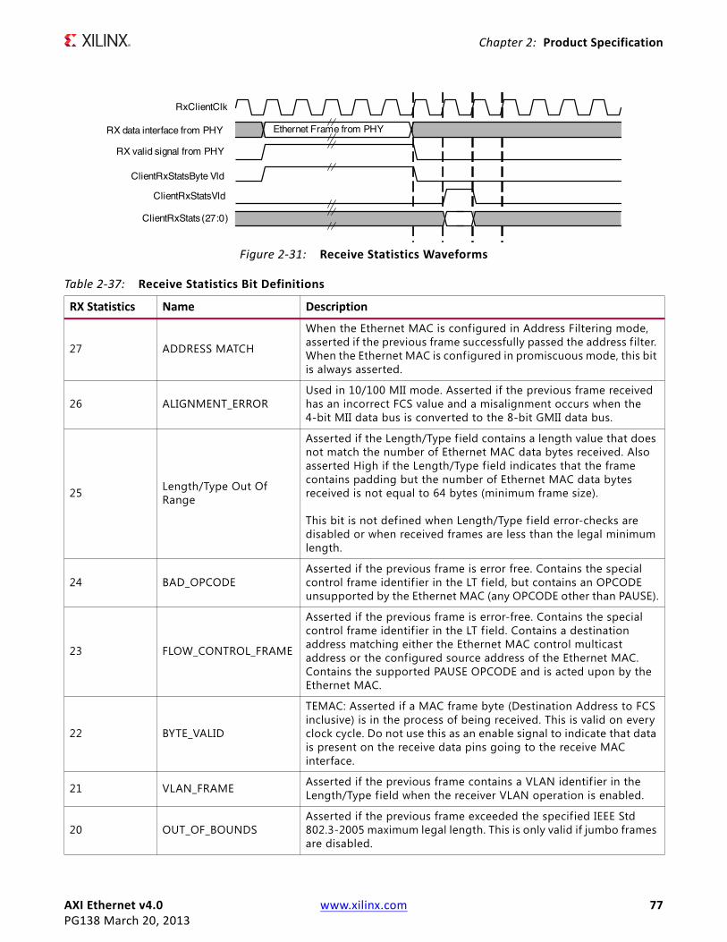
AXI Ethernet v4.0 www.xilinx.com 77PG138 March 20, 2013
Chapter 2: Product Specification
X-Ref Target - Figure 2-31
Figure 2‐31: Receive Statistics Waveforms
RX data interface from PHY
RxClientClk
ClientRxStatsByte Vld
RX valid signal from PHY
ClientRxStats (27:0)
ClientRxStatsVld
Ethernet Frame from PHY
Table 2‐37: Receive Statistics Bit Definitions
RX Statistics Name Description
27 ADDRESS MATCH
When the Ethernet MAC is configured in Address Filtering mode, asserted if the previous frame successfully passed the address filter. When the Ethernet MAC is configured in promiscuous mode, this bit is always asserted.
26 ALIGNMENT_ERRORUsed in 10/100 MII mode. Asserted if the previous frame received has an incorrect FCS value and a misalignment occurs when the 4-bit MII data bus is converted to the 8-bit GMII data bus.
25 Length/Type Out Of Range
Asserted if the Length/Type f ield contains a length value that does not match the number of Ethernet MAC data bytes received. Also asserted High if the Length/Type field indicates that the frame contains padding but the number of Ethernet MAC data bytes received is not equal to 64 bytes (minimum frame size).
This bit is not defined when Length/Type f ield error-checks are disabled or when received frames are less than the legal minimum length.
24 BAD_OPCODEAsserted if the previous frame is error free. Contains the special control frame identif ier in the LT f ield, but contains an OPCODE unsupported by the Ethernet MAC (any OPCODE other than PAUSE).
23 FLOW_CONTROL_FRAME
Asserted if the previous frame is error-free. Contains the special control frame identif ier in the LT f ield. Contains a destination address matching either the Ethernet MAC control multicast address or the configured source address of the Ethernet MAC. Contains the supported PAUSE OPCODE and is acted upon by the Ethernet MAC.
22 BYTE_VALID
TEMAC: Asserted if a MAC frame byte (Destination Address to FCS inclusive) is in the process of being received. This is valid on every clock cycle. Do not use this as an enable signal to indicate that data is present on the receive data pins going to the receive MAC interface.
21 VLAN_FRAME Asserted if the previous frame contains a VLAN identif ier in the Length/Type field when the receiver VLAN operation is enabled.
20 OUT_OF_BOUNDSAsserted if the previous frame exceeded the specif ied IEEE Std 802.3-2005 maximum legal length. This is only valid if jumbo frames are disabled.

AXI Ethernet v4.0 www.xilinx.com 78PG138 March 20, 2013
Chapter 2: Product Specification
19 CONTROL_FRAME Asserted if the previous frame contains the special control frame identif ier in the Length/Type f ield.
18 - 5 FRAME_LENGTH_COUNT The length of the previous frame in number of bytes. The count sticks at 16383 for any jumbo frames larger than this value.
4 MULTICAST_FRAME Asserted if the previous frame contains a multicast address in the destination f ield.
3 BROADCAST_FRAME Asserted if the previous frame contains the broadcast address in the destination f ield.
2 FCS_ERROR Asserted if the previous frame received has an incorrect FCS value or the Ethernet MAC detects error codes during frame reception.
1 BAD_FRAME(1) Asserted if the previous frame received contains errors.
0 GOOD_FRAME(1) Asserted if the previous frame received is error free.
Notes: 1. If the length/type f ield error checks are disabled, then a frame containing this type of error is marked as a GOOD_FRAME,
providing no additional errors were detected.
Table 2‐37: Receive Statistics Bit Definitions (Cont’d)
RX Statistics Name Description
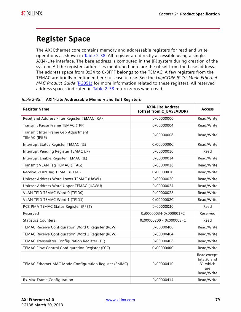
AXI Ethernet v4.0 www.xilinx.com 79PG138 March 20, 2013
Chapter 2: Product Specification
Register SpaceThe AXI Ethernet core contains memory and addressable registers for read and write operations as shown in Table 2-38. All register are directly accessible using a single AXI4-Lite interface. The base address is computed in the IPI system during creation of the system. All the registers addresses mentioned here are the offset from the base address. The address space from 0x34 to 0x3FFF belongs to the TEMAC. A few registers from the TEMAC are briefly mentioned here for ease of use. See the LogiCORE IP Tri-Mode Ethernet MAC Product Guide (PG051) for more information related to these registers. All reserved address spaces indicated in Table 2-38 return zeros when read.
Table 2‐38: AXI4‐Lite Addressable Memory and Soft Registers
Register Name AXI4‐Lite Address (offset from C_BASEADDR)
Access
Reset and Address Filter Register TEMAC (RAF) 0x00000000 Read/Write
Transmit Pause Frame TEMAC (TPF) 0x00000004 Read/Write
Transmit Inter Frame Gap Adjustment TEMAC (IFGP)
0x00000008 Read/Write
Interrupt Status Register TEMAC (IS) 0x0000000C Read/Write
Interrupt Pending Register TEMAC (IP) 0x00000010 Read
Interrupt Enable Register TEMAC (IE) 0x00000014 Read/Write
Transmit VLAN Tag TEMAC (TTAG) 0x00000018 Read/Write
Receive VLAN Tag TEMAC (RTAG) 0x0000001C Read/Write
Unicast Address Word Lower TEMAC (UAWL) 0x00000020 Read/Write
Unicast Address Word Upper TEMAC (UAWU) 0x00000024 Read/Write
VLAN TPID TEMAC Word 0 (TPID0) 0x00000028 Read/Write
VLAN TPID TEMAC Word 1 (TPID1) 0x0000002C Read/Write
PCS PMA TEMAC Status Register (PPST) 0x00000030 Read
Reserved 0x00000034-0x000001FC Reserved
Statistics Counters 0x00000200 - 0x000003FC Read
TEMAC Receive Configuration Word 0 Register (RCW) 0x00000400 Read/Write
TEMAC Receive Configuration Word 1 Register (RCW) 0x00000404 Read/Write
TEMAC Transmitter Configuration Register (TC) 0x00000408 Read/Write
TEMAC Flow Control Configuration Register (FCC) 0x0000040C Read/Write
TEMAC Ethernet MAC Mode Configuration Register (EMMC) 0x00000410
Read except bits 30 and 31 which
are Read/Write
Rx Max Frame Configuration 0x00000414 Read/Write

AXI Ethernet v4.0 www.xilinx.com 80PG138 March 20, 2013
Chapter 2: Product Specification
Tx Max Frame Configuration 0x00000418 Read/Write
RGMII/SGMII Configuration 0x00000420 Read
Reserved 0x0000041C-0x000004F4 Reserved
Identif ication Register 0x000004F8 Read
Ability Register 0x000004FC Read
MII Management Configuration Register 0x00000500 Read/Write
MII Management Control 0x00000504 Read/Write
MII Management Write Data 0x00000508 Read/Write
MII Management Read Data 0x0000050C Read
Reserved 0x00000510-0x000005FC Reserved
MDIO Interrupt Status Register (MIS) 0x00000600 Read/Write
Reserved 0x00000604-0x0000061C Reserved
MDIO Interrupt Pending Register (MIP) 0x00000620 Read
Reserved 0x00000624-0x0000063C Reserved
MDIO Interrupt Enable Register (MIE) 0x00000640 Read/Write
Reserved 0x00000644-0x0000065C Reserved
MDIO Interrupt Clear Register (MIC) 0x00000660 Read/Write
Reserved 0x00000664-0x000006FC Reserved
TEMAC Unicast Address Word 0 Register (UAW0) 0x00000700 Read/Write
TEMAC Unicast Address Word 1 Register (UAW1) 0x00000704 Read/Write
Filter Mask Index (FMI) 0x00000708 Read/Write
Reserved 0x0000070C Reserved
Address Filter (31:0) 0x00000710 Read/Write
Address Filter (47:32) 0x00000714 Read/Write
Reserved 0x00000718 - 0x0000078C Read/Write
Reserved 0x00000790-0x00000FFC Reserved
Reserved 0x00001000-0x00003FFC Reserved
Transmit VLAN Data Table TEMAC 0x00004000 - 0x00007FFC Read/Write
Receive VLAN Data Table TEMAC 0x00008000 - 0x0000BFFC Read/Write
Reserved 0x0000C000-0x0000FFFC Reserved
Ethernet AVB 0x00010000-0x00013FFC Read/Write
Reserved 0x00014000-0x0001FFFC Reserved
Multicast Address Table TEMAC 0x00020000 - 0x0003FFFC Read/Write
Table 2‐38: AXI4‐Lite Addressable Memory and Soft Registers (Cont’d)
Register Name AXI4‐Lite Address (offset from C_BASEADDR)
Access

AXI Ethernet v4.0 www.xilinx.com 81PG138 March 20, 2013
Chapter 2: Product Specification
Reset and Address Filter Register ‐ Offset 0x0000_0000
The Reset and Address Filter (RAF) register is shown in Figure 2-33. This register allows the software to block receive multicast and broadcast Ethernet frames. Additional receive address f iltering is provided with the registers in Table 2-73 and Table 2-74. The multicast reject bit provides a means of blocking receive multicast Ethernet frames without having to clear out any multicast address values stored in the multicast address table. It also provides a means for allowing more than four multicast addresses to be received (the limit of the multicast address table). To accept more than four multicast addresses, the FMI register would be set to promiscuous mode and the multicast reject bit of this register set to allow multicast frames. See Extended Multicast Address Filtering Mode for more information. Software might also need to filter out additional receive frames with other addresses. The broadcast reject bit provides the only means for rejecting receive broadcast Ethernet frames.
X-Ref Target - Figure 2-32
Figure 2‐32: Address Mapping Diagram

AXI Ethernet v4.0 www.xilinx.com 82PG138 March 20, 2013
Chapter 2: Product Specification
As additional functionality was added to the core, this register became the convenient location for new bits to control those new functions. Care has been taken to minimize the effect of these new bits on existing applications by ensuring that the default values of these bits disable new functionality. This setting ensures that when applications do not use the new bits, the core operates the way it did previously.
Table 2-39 shows the Reset and Address Filter Register bit definitions.
X-Ref Target - Figure 2-33
Figure 2‐33: Reset and Address Filter Register (offset 0x0000_0000)
1231 15 13 1011
Reserved
BcstRejRxBadFrmEn
McstRej
DS759_04
MS
B
LSB
9 8 7 6 5 4 314 2 1 0
TxVTagMode
RxVTagMode
TxVStrpMode
RxVStrpMode
NewFncEnbl
EMultiFltrEnbl
ReservedReserved
Table 2‐39: Reset and Address Filter Register Bit Definitions
Bits NameCoreAccess
ResetValue
Description
31 - 15 Reserved Read 0x0 Reserved: These bits are reserved for future use and always return zero.
14 RxBadFrmEn Read/Write 0
Receive Bad Frame Enable. This bit provides a means for allowing bad receive frames to be accepted and passed to the RX AXI4-Stream interface as if they were good frames.0 - Normal operation, bad frames are rejected.1 - Bad frames are accepted.
13 Reserved Read 0 Reserved: These bits are reserved for future use and always return zero.
12 EMultiFltrEnbl Read/Write 0
Enhanced Multicast Filter Enable: This bit provides a simple way to disable the new enhanced multicast f iltering if present. This is necessary if promiscuous address reception mode is desired or if use of the built-in 4 TEMAC multicast address registers is required when the core includes the enhanced multicast address filtering function enabled at build time by the C_MCAST_EXTEND parameters. See Extended Multicast Address Filtering Mode for more details.0 - Disable enhanced multicast address filtering mode.1 - Enable enhanced multicast address f iltering mode if present.
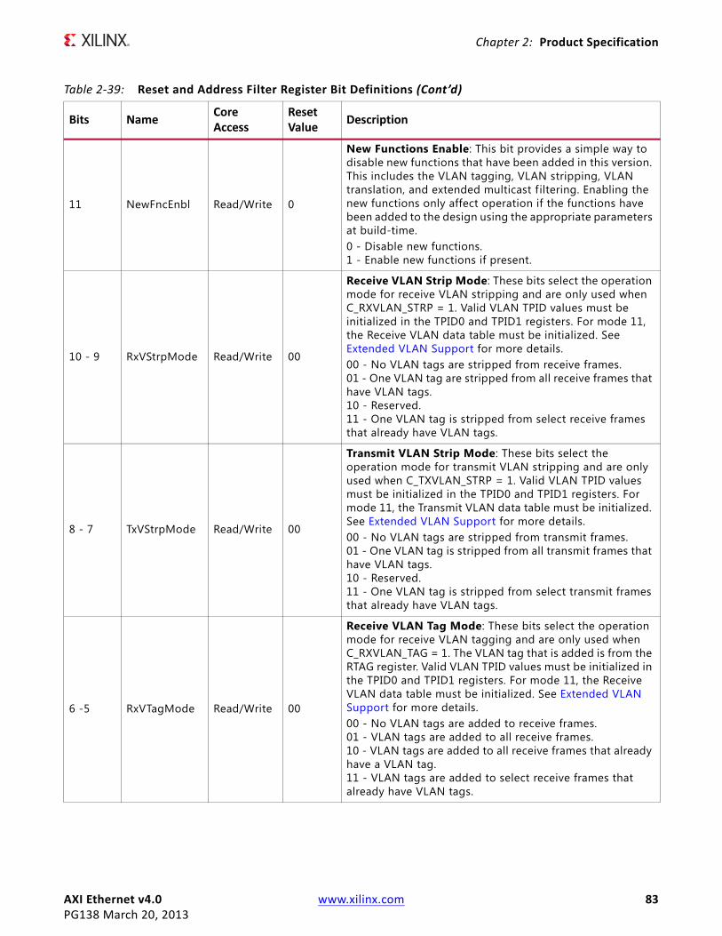
AXI Ethernet v4.0 www.xilinx.com 83PG138 March 20, 2013
Chapter 2: Product Specification
11 NewFncEnbl Read/Write 0
New Functions Enable: This bit provides a simple way to disable new functions that have been added in this version. This includes the VLAN tagging, VLAN stripping, VLAN translation, and extended multicast f iltering. Enabling the new functions only affect operation if the functions have been added to the design using the appropriate parameters at build-time. 0 - Disable new functions.1 - Enable new functions if present.
10 - 9 RxVStrpMode Read/Write 00
Receive VLAN Strip Mode: These bits select the operation mode for receive VLAN stripping and are only used when C_RXVLAN_STRP = 1. Valid VLAN TPID values must be initialized in the TPID0 and TPID1 registers. For mode 11, the Receive VLAN data table must be initialized. See Extended VLAN Support for more details.00 - No VLAN tags are stripped from receive frames.01 - One VLAN tag are stripped from all receive frames that have VLAN tags.10 - Reserved.11 - One VLAN tag is stripped from select receive frames that already have VLAN tags.
8 - 7 TxVStrpMode Read/Write 00
Transmit VLAN Strip Mode: These bits select the operation mode for transmit VLAN stripping and are only used when C_TXVLAN_STRP = 1. Valid VLAN TPID values must be initialized in the TPID0 and TPID1 registers. For mode 11, the Transmit VLAN data table must be initialized. See Extended VLAN Support for more details.00 - No VLAN tags are stripped from transmit frames.01 - One VLAN tag is stripped from all transmit frames that have VLAN tags.10 - Reserved.11 - One VLAN tag is stripped from select transmit frames that already have VLAN tags.
6 -5 RxVTagMode Read/Write 00
Receive VLAN Tag Mode: These bits select the operation mode for receive VLAN tagging and are only used when C_RXVLAN_TAG = 1. The VLAN tag that is added is from the RTAG register. Valid VLAN TPID values must be initialized in the TPID0 and TPID1 registers. For mode 11, the Receive VLAN data table must be initialized. See Extended VLAN Support for more details.00 - No VLAN tags are added to receive frames.01 - VLAN tags are added to all receive frames.10 - VLAN tags are added to all receive frames that already have a VLAN tag.11 - VLAN tags are added to select receive frames that already have VLAN tags.
Table 2‐39: Reset and Address Filter Register Bit Definitions (Cont’d)
Bits NameCoreAccess
ResetValue
Description
AXI Ethernet v4.0 www.xilinx.com 84PG138 March 20, 2013
Chapter 2: Product Specification
Transmit Pause Frame Register ‐ Offset 0x0000_0004
The Transmit Pause Frame (TPF) TEMAC Register is shown in Figure 2-34. This register provides a value of pause when enabled by the FCC register (page 107). When enabled, the Ethernet transmits a pause frame whenever this register is written. Pause values are defined in units of pause quanta which are defined as 512 bit times for the current transmission speed. Therefore, pause times can have values ranging from 0 to 65,535 * 512 bit times.
4 - 3 TxVTagMode Read/Write 00
Transmit VLAN Tag Mode: These bits select the operation mode for transmit VLAN tagging and are only used when C_TXVLAN_TAG = 1. The VLAN tag that is added is from the TTAG register. Valid VLAN TPID values must be initialized in the TPID0 and TPID1 registers. For mode 11, the Transmit VLAN data table must be initialized. See Extended VLAN Support for more details.00 - No VLAN tags are added to transmit frames.01 - VLAN tags are added to all transmit frames.10 - VLAN tags are added to all transmit frames that already have a VLAN tag.11 - VLAN tags are added to select transmit frames that already have VLAN tags.
2 BcstRej Read/Write 0
Reject Receive Broadcast Destination Address: This bit provides a means for accepting or rejecting broadcast Ethernet frames. 0 - Accept receive broadcast destination address Ethernet frames.1 - Reject all receive broadcast destination address Ethernet frames. This is the only method available for blocking broadcast Ethernet frames.
1 McstRej Read/Write 0
Reject Receive Multicast Destination Address: This bit provides a means for accepting or rejecting multicast Ethernet frames. 0 - Accept receive multicast destination address Ethernet frames that meet address f iltering specified in FMI register and/or the multicast address table.1 - Reject all receive multicast destination address Ethernet frames regardless of FMI register and multicast address table.
0 Reserved Read 0 Reserved: These bits are reserved for future definition and always return zero.
Table 2‐39: Reset and Address Filter Register Bit Definitions (Cont’d)
Bits NameCoreAccess
ResetValue
Description

AXI Ethernet v4.0 www.xilinx.com 85PG138 March 20, 2013
Chapter 2: Product Specification
Table 2-40 shows the Transmit Pause Frame Register bit definitions.
Transmit Inter Frame Gap Adjustment Register ‐ Offset 0x0000_0008
The Transmit Inter Frame Gap Adjustment (IFGP) Register is shown in Figure 2-35. This register provides a duration value of Inter Frame Gap when enabled by the TC register (page 105). When enabled, the TEMAC uses the value of this register to extend the Inter Frame Gap beyond the minimum of 12 idle cycles which is 96-bit times on the Ethernet Interface.
Table 2-41 shows the Transmit Inter Frame Gap Adjustment Register bit definitions.
X-Ref Target - Figure 2-34
Figure 2‐34: Transmit Pause Frame Register (offset 0x0000_0004)
31
Reserved
16 15 0
TPFV DS759_05
MS
B
LSB
Table 2‐40: Transmit Pause Frame Register Bit Definitions
Bits Name Core AccessReset Value
Description
31 - 16 Reserved Read 0x0 Reserved: These bits are reserved for future use and always return zero.
15 - 0 TPFV Read/Write 0x0
Transmit Pause Frame Value: These bits denote the value of the transmit pause frame pause time in units of 512 bit times. If enabled by the FCC register, writing a value into this register initiates the transmission of a single pause frame with the pause value defined in this f ield.
X-Ref Target - Figure 2-35
Figure 2‐35: Transmit Inter Frame Gap Adjustment Register (offset 0x0000_0008)
31
Reserved IFGPDS759_06
MS
B
LSB
8 7 0
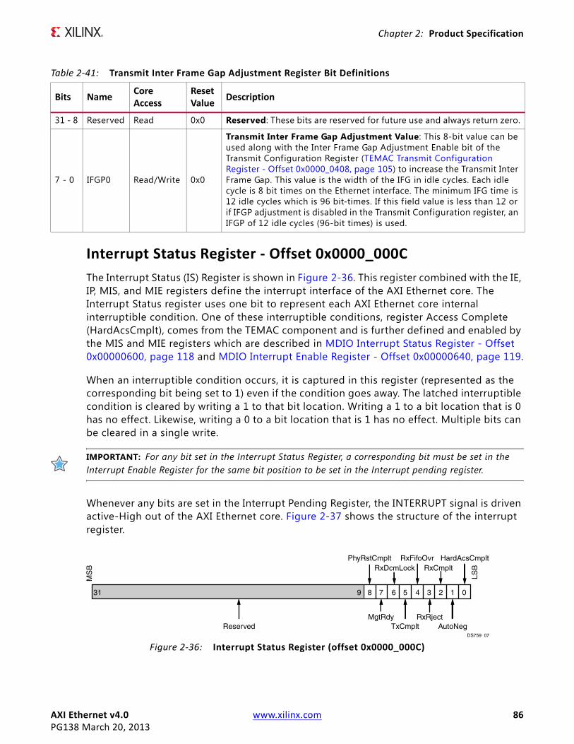
AXI Ethernet v4.0 www.xilinx.com 86PG138 March 20, 2013
Chapter 2: Product Specification
Interrupt Status Register ‐ Offset 0x0000_000C
The Interrupt Status (IS) Register is shown in Figure 2-36. This register combined with the IE, IP, MIS, and MIE registers define the interrupt interface of the AXI Ethernet core. The Interrupt Status register uses one bit to represent each AXI Ethernet core internal interruptible condition. One of these interruptible conditions, register Access Complete (HardAcsCmplt), comes from the TEMAC component and is further defined and enabled by the MIS and MIE registers which are described in MDIO Interrupt Status Register - Offset 0x00000600, page 118 and MDIO Interrupt Enable Register - Offset 0x00000640, page 119.
When an interruptible condition occurs, it is captured in this register (represented as the corresponding bit being set to 1) even if the condition goes away. The latched interruptible condition is cleared by writing a 1 to that bit location. Writing a 1 to a bit location that is 0 has no effect. Likewise, writing a 0 to a bit location that is 1 has no effect. Multiple bits can be cleared in a single write.
IMPORTANT: For any bit set in the Interrupt Status Register, a corresponding bit must be set in the Interrupt Enable Register for the same bit position to be set in the Interrupt pending register.
Whenever any bits are set in the Interrupt Pending Register, the INTERRUPT signal is driven active-High out of the AXI Ethernet core. Figure 2-37 shows the structure of the interrupt register.
Table 2‐41: Transmit Inter Frame Gap Adjustment Register Bit Definitions
Bits NameCoreAccess
ResetValue
Description
31 - 8 Reserved Read 0x0 Reserved: These bits are reserved for future use and always return zero.
7 - 0 IFGP0 Read/Write 0x0
Transmit Inter Frame Gap Adjustment Value: This 8-bit value can be used along with the Inter Frame Gap Adjustment Enable bit of the Transmit Configuration Register (TEMAC Transmit Configuration Register - Offset 0x0000_0408, page 105) to increase the Transmit Inter Frame Gap. This value is the width of the IFG in idle cycles. Each idle cycle is 8 bit times on the Ethernet interface. The minimum IFG time is 12 idle cycles which is 96 bit-times. If this f ield value is less than 12 or if IFGP adjustment is disabled in the Transmit Configuration register, an IFGP of 12 idle cycles (96-bit times) is used.
X-Ref Target - Figure 2-36
Figure 2‐36: Interrupt Status Register (offset 0x0000_000C)
8931 7 6
Reserved
HardAcsCmplt
AutoNeg
5 4 2 1 03
RxRject
RxCmpltRxFifoOvrPhyRstCmplt
RxDcmLock
TxCmpltMgtRdy
DS759_07
MS
B
LSB

AXI Ethernet v4.0 www.xilinx.com 87PG138 March 20, 2013
Chapter 2: Product Specification
Table 2-42 shows the Interrupt Status Register bit definitions.
Table 2‐42: Interrupt Status Register Bit Definitions
Bits NameCoreAccess
ResetValue
Description
31 - 9 Reserved Read 0x0 Reserved: These bits are reserved for future use and always return zero.
8 PhyRstCmplt Read/Write 0
PHY Reset Complete. When set to 1, this bit indicates the PHY can be accessed. This signal does not transition to 1 for 5 ms after PHY_RST_N transitions to 1.0 - PHY not ready1 - PHY ready
7 MgtRdy(1) Read/Write 0 / 1
Serial Transceiver Ready: This bit indicates if the TEMAC is out of reset and ready for use. In systems that use a serial transceiver, this bit goes to 1 when the serial transceiver is ready to use. Prior to that time, access of TEMAC registers does not complete and the core does not operate. In systems that do not use an serial transceiver, this signal goes to 1 immediately after reset.0 - serial transceiver / TEMAC not ready1 - serial transceiver / TEMAC ready
6 RxDcmLock Read/Write 1
Receive DCM Lock: No longer used, but reserved for future use. This bit is always one.0 - Rx DCM not locked1 - Rx DCM Locked
5 TxCmplt Read/Write 0
Transmit Complete: This bit indicates that a frame was successfully transmitted.0 - no frame transmitted1 - frame transmitted
4 RxMemOvr Read/Write 0
Receive Memory Overrun: This bit indicates that the receive Memory overflowed while receiving an Ethernet frame.0 - normal operation, no overflow occurred1 - receive Memory overflow occurred and data was lost
3 RxRject(2) Read/Write 0
Receive Frame Rejected: This bit indicates that a receive frame was rejected.0 - no receive frame rejected1 - receive frame was rejected
2 RxCmplt Read/Write 0
Receive Complete: This bit indicates that a packet was successfully received.0 - no frame received1 - frame received
1 AutoNeg Read/Write 0
Auto Negotiation Complete: This bit indicates that auto negotiation of the SGMII or 1000 Base-X interface has completed.0 - auto negotiation not complete1 - auto negotiation complete
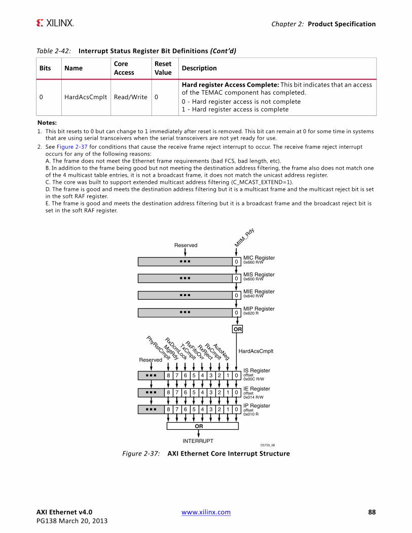
AXI Ethernet v4.0 www.xilinx.com 88PG138 March 20, 2013
Chapter 2: Product Specification
0 HardAcsCmplt Read/Write 0
Hard register Access Complete: This bit indicates that an access of the TEMAC component has completed.0 - Hard register access is not complete1 - Hard register access is complete
Notes: 1. This bit resets to 0 but can change to 1 immediately after reset is removed. This bit can remain at 0 for some time in systems
that are using serial transceivers when the serial transceivers are not yet ready for use.2. See Figure 2-37 for conditions that cause the receive frame reject interrupt to occur. The receive frame reject interrupt
occurs for any of the following reasons:A. The frame does not meet the Ethernet frame requirements (bad FCS, bad length, etc).B. In addition to the frame being good but not meeting the destination address f iltering, the frame also does not match one of the 4 multicast table entries, it is not a broadcast frame, it does not match the unicast address register.C. The core was built to support extended multicast address f iltering (C_MCAST_EXTEND=1).D. The frame is good and meets the destination address f iltering but it is a multicast frame and the multicast reject bit is set in the soft RAF register.E. The frame is good and meets the destination address f iltering but it is a broadcast frame and the broadcast reject bit is set in the soft RAF register.
Table 2‐42: Interrupt Status Register Bit Definitions (Cont’d)
Bits NameCoreAccess
ResetValue
Description
X-Ref Target - Figure 2-37
Figure 2‐37: AXI Ethernet Core Interrupt Structure
Reserved
Reserved
...
...
0
MIIM
_Rdy
0
IS Registeroffset0x00C R/W
MIP Register0x620 R
MIS Register0x600 R/W
IE Registeroffset0x014 R/W
IP Registeroffset0x010 R
OR
8 7 6 5 4 3
AutoNeg
RxCmplt
RxRject
RxFifoOvr
TxCmplt
2
RxDcmLock
PhyRstCmplt
1 0
... 8 7 6 5 4 3 2 1 0
... 8 7 6 5 4 3 2 1 0
MgtRdy
HardAcsCmplt
OR
INTERRUPT
...0
MIE Register0x640 R/W...
0MIC Register0x660 R/W...
DS759_08
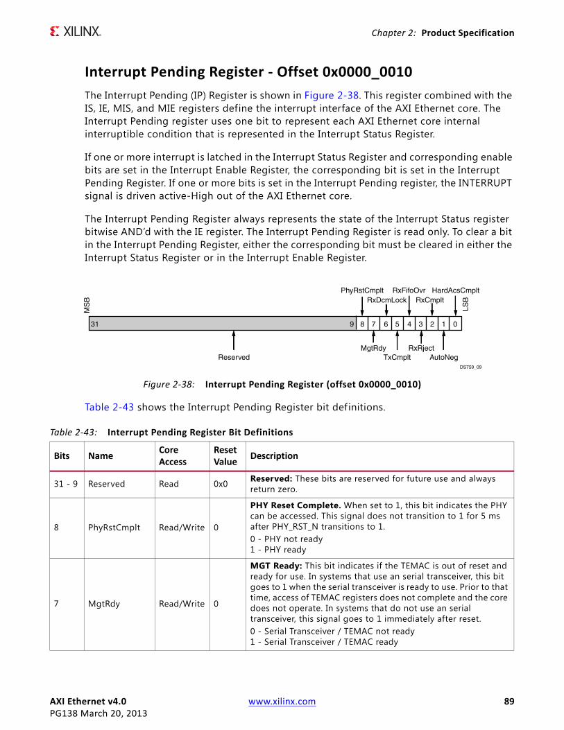
AXI Ethernet v4.0 www.xilinx.com 89PG138 March 20, 2013
Chapter 2: Product Specification
Interrupt Pending Register ‐ Offset 0x0000_0010
The Interrupt Pending (IP) Register is shown in Figure 2-38. This register combined with the IS, IE, MIS, and MIE registers define the interrupt interface of the AXI Ethernet core. The Interrupt Pending register uses one bit to represent each AXI Ethernet core internal interruptible condition that is represented in the Interrupt Status Register.
If one or more interrupt is latched in the Interrupt Status Register and corresponding enable bits are set in the Interrupt Enable Register, the corresponding bit is set in the Interrupt Pending Register. If one or more bits is set in the Interrupt Pending register, the INTERRUPT signal is driven active-High out of the AXI Ethernet core.
The Interrupt Pending Register always represents the state of the Interrupt Status register bitwise AND’d with the IE register. The Interrupt Pending Register is read only. To clear a bit in the Interrupt Pending Register, either the corresponding bit must be cleared in either the Interrupt Status Register or in the Interrupt Enable Register.
Table 2-43 shows the Interrupt Pending Register bit definitions.
X-Ref Target - Figure 2-38
Figure 2‐38: Interrupt Pending Register (offset 0x0000_0010)
8931 7 6
Reserved
HardAcsCmplt
AutoNeg
5 4 2 1 03
RxRject
RxCmpltRxFifoOvrPhyRstCmplt
RxDcmLock
TxCmpltMgtRdy
DS759_09
MS
B
LSB
Table 2‐43: Interrupt Pending Register Bit Definitions
Bits NameCoreAccess
ResetValue
Description
31 - 9 Reserved Read 0x0 Reserved: These bits are reserved for future use and always return zero.
8 PhyRstCmplt Read/Write 0
PHY Reset Complete. When set to 1, this bit indicates the PHY can be accessed. This signal does not transition to 1 for 5 ms after PHY_RST_N transitions to 1.0 - PHY not ready1 - PHY ready
7 MgtRdy Read/Write 0
MGT Ready: This bit indicates if the TEMAC is out of reset and ready for use. In systems that use an serial transceiver, this bit goes to 1 when the serial transceiver is ready to use. Prior to that time, access of TEMAC registers does not complete and the core does not operate. In systems that do not use an serial transceiver, this signal goes to 1 immediately after reset.0 - Serial Transceiver / TEMAC not ready1 - Serial Transceiver / TEMAC ready

AXI Ethernet v4.0 www.xilinx.com 90PG138 March 20, 2013
Chapter 2: Product Specification
Interrupt Enable Register ‐ Offset 0x0000_0014
The Interrupt Enable (IE) Register is shown in Figure 2-39. This register, combined with the IS, IP, MIS, and MIE registers, define the interrupt interface of the AXI Ethernet core. The Interrupt Enable register uses one bit to represent each AXI Ethernet core internal interruptible condition represented in the Interrupt Status Register. Each bit set in the Interrupt Enable Register allows an interruptible condition bit in the Interrupt Status Register to pass through to the Interrupt Pending Register.
6 RxDcmLock Read/Write 0
Receive DCM Lock: No longer used, but reserved for future use. This bit is always one.0 - Rx DCM not locked1 - Rx DCM Locked
5 TxCmplt Read/Write 0
Transmit Complete: This bit indicates that a frame was successfully transmitted.0 - no frame transmitted1 - frame transmitted
4 RxMemOvr Read/Write 0
Receive Memory Overrun: This bit indicates that the receive Memory overflowed while receiving an Ethernet frame.0 - normal operation, no overflow occurred1 - receive Memory overflow occurred and data was lost
3 RxRject Read/Write 0
Receive Frame Rejected: This bit indicates that a receive frame was rejected.0 - no receive frame rejected1 - receive frame was rejected
2 RxCmplt Read/Write 0
Receive Complete: This bit indicates that a packet was successfully received. 0 - no frame received1 - frame received
1 AutoNeg Read/Write 0
Auto Negotiation Complete: This bit indicates that auto negotiation of the SGMII or 1000 Base-X interface has completed.0 - auto negotiation not complete1 - auto negotiation complete
0 HardAcsCmplt Read/Write 0
Hard register Access Complete: This bit indicates that an access of the TEMAC component has completed.0 - Hard register access is not complete1 - Hard register access is complete
Table 2‐43: Interrupt Pending Register Bit Definitions (Cont’d)
Bits NameCoreAccess
ResetValue
Description

AXI Ethernet v4.0 www.xilinx.com 91PG138 March 20, 2013
Chapter 2: Product Specification
Table 2-44 shows the Interrupt Enable Register bit definitions.
X-Ref Target - Figure 2-39
Figure 2‐39: Interrupt Enable Register (offset 0x0000_0014)
8931 7 6
Reserved
HardAcsCmplt
AutoNeg
5 4 2 1 03
RxRject
RxCmpltRxFifoOvrPhyRstCmplt
RxDcmLock
TxCmpltMgtRdy
DS759_10
MS
B
LSB
Table 2‐44: Interrupt Enable Register Bit Definitions
Bits NameCore Access
Reset Value
Description
31 - 9 Reserved Read 0x0 Reserved: These bits are reserved for future definition and always return zero.
8 PhyRstCmplt Read/Write 0PHY Reset Complete: Bit used to enable interrupt.0 - Interrupt Disabled1 - Interrupt Enabled
7 MgtRdy Read/Write 0 MGT Ready: Bit used to enable interrupt.0 - Interrupt Disabled1 - Interrupt Enabled
6 RxDcmLock Read/Write 0Receive DCM Lock: Bit used to enable interrupt.0 - Interrupt Disabled1 - Interrupt Enabled
5 TxCmplt Read/Write 0Transmit Complete: Bit used to enable interrupt.0 - Interrupt Disabled1 - Interrupt Enabled
4 RxMemOvr Read/Write 0Receive Memory Overrun: Bit used to enable interrupt.0 - Interrupt Disabled1 - Interrupt Enabled
3 RxRject Read/Write 0Receive Frame Rejected: Bit used to enable interrupt.0 - Interrupt Disabled1 - Interrupt Enabled
2 RxCmplt Read/Write 0Receive Complete: Bit used to enable interrupt.0 - Interrupt Disabled1 - Interrupt Enabled
1 AutoNeg Read/Write 0Auto Negotiation Complete: Bit used to enable interrupt.0 - Interrupt Disabled1 - Interrupt Enabled
0 HardAcsCmplt Read/Write 0Hard register Access Complete: Bit used to enable interrupt.0 - Interrupt Disabled1 - Interrupt Enabled
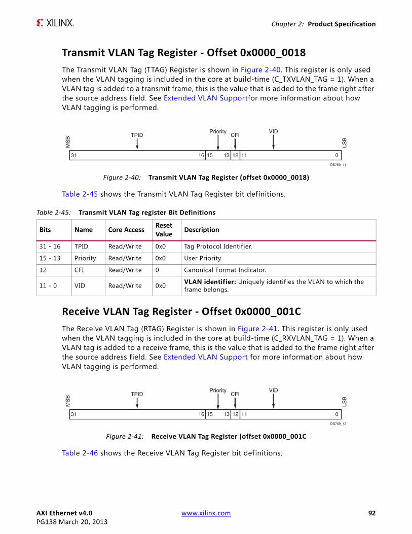
AXI Ethernet v4.0 www.xilinx.com 92PG138 March 20, 2013
Chapter 2: Product Specification
Transmit VLAN Tag Register ‐ Offset 0x0000_0018
The Transmit VLAN Tag (TTAG) Register is shown in Figure 2-40. This register is only used when the VLAN tagging is included in the core at build-time (C_TXVLAN_TAG = 1). When a VLAN tag is added to a transmit frame, this is the value that is added to the frame right after the source address field. See Extended VLAN Supportfor more information about how VLAN tagging is performed.
Table 2-45 shows the Transmit VLAN Tag Register bit definitions.
Receive VLAN Tag Register ‐ Offset 0x0000_001C
The Receive VLAN Tag (RTAG) Register is shown in Figure 2-41. This register is only used when the VLAN tagging is included in the core at build-time (C_RXVLAN_TAG = 1). When a VLAN tag is added to a receive frame, this is the value that is added to the frame right after the source address field. See Extended VLAN Support for more information about how VLAN tagging is performed.
Table 2-46 shows the Receive VLAN Tag Register bit definitions.
X-Ref Target - Figure 2-40ds759_11.eps
Figure 2‐40: Transmit VLAN Tag Register (offset 0x0000_0018)
DS759_11
MS
B
LSB
VIDPriorityCFITPID
111216 1315 031
Table 2‐45: Transmit VLAN Tag register Bit Definitions
Bits Name Core AccessReset Value
Description
31 - 16 TPID Read/Write 0x0 Tag Protocol Identif ier.
15 - 13 Priority Read/Write 0x0 User Priority.
12 CFI Read/Write 0 Canonical Format Indicator.
11 - 0 VID Read/Write 0x0 VLAN identifier: Uniquely identif ies the VLAN to which the frame belongs.
X-Ref Target - Figure 2-41
Figure 2‐41: Receive VLAN Tag Register (offset 0x0000_001C
DS759_12
MS
B
LSB
VIDPriorityCFITPID
111216 1315 031
AXI Ethernet v4.0 www.xilinx.com 93PG138 March 20, 2013
Chapter 2: Product Specification
Unicast Address Word Lower Register ‐ Offset 0x0000_0020
The Unicast Address Word Lower (UAWL) Register is shown in Figure 2-42. This register and the Unicast Address Word Upper (UAWU) Register are only used when extended multicast filtering is included in the core at build-time (C_MCAST_EXTEND = 1) and is enabled. These registers should not be confused with the UAW0 and UAW1 registers which are registers inside the TEMAC core which are only used when extended multicast filtering is excluded in the core at build-time or is disabled.
IMPORTANT: When using extended multicast filtering, the TEMAC core must be placed in promiscuous address filtering mode.
This register allows f iltering of unicast frames not matching the address stored in these registers. See Extended Multicast Address Filtering Mode for more information.
Table 2-47 shows the Unicast Address Word Lower Register bit definitions.
Table 2‐46: Receive VLAN Tag Register Bit Definitions
Bits Name Core AccessReset Value
Description
31 - 16 TPID Read/Write 0x0 Tag Protocol Identif ier.
15 - 13 Priority Read/Write 0x0 User Priority.
12 CFI Read/Write 0 Canonical Format Indicator.
11 - 0 VID Read/Write 0x0 VLAN identifier: Uniquely identif ies the VLAN to which the frame belongs
X-Ref Target - Figure 2-42
Figure 2‐42: Unicast Address Word Lower Register (offset 0x020)
031
UnicastAddr(31:0)DS759_13
MS
B
LSB
Table 2‐47: Unicast Address Word Lower Register Bit Definitions
Bits NameCore Access
Reset Value Description
31 - 0 UnicastAddr Read/Write 0x00000000
Unicast Address (31:0): This address is used to match against the destination address of any received frames.The address is ordered so the f irst byte transmitted/received is the lowest positioned byte in the register; for example, a MAC address of AA-BB-CC-DD-EE-FF would be stored in UnicastAddr(47:0) as 0xFFEEDDCCBBAA.
AXI Ethernet v4.0 www.xilinx.com 94PG138 March 20, 2013
Chapter 2: Product Specification
Unicast Address Word Upper Register ‐ Offset 0x0000_0024
The Unicast Address Word Upper (UAWU) Register is shown in Figure 2-43. This register and the register are only used when extended multicast f iltering is included in the core at build-time (C_MCAST_EXTEND = 1).
IMPORTANT: When using extended multicast filtering, the TEMAC core must be placed in promiscuous address filtering mode.
This register allows f iltering of unicast frames not matching the address stored in these registers. See Extended Multicast Address Filtering Mode for more information.
Table 2-48 shows the Unicast Address Word Upper Register bit definitions.
VLAN TPID Word 0 Register ‐ Offset 0x0000_0028
The VLAN TPID Word 0 (TPID0) Register is shown in Figure 2-44. This register is only used when transmit and/or receive VLAN functions are included in the core at build-time (C_TXVLAN_TAG = 1 and/or C_RXVLAN_TAG = 1 and/or C_TXVLAN_STRP= 1 and/or C_RXVLAN_STRP= 1 and/or C_TXVLAN_TRAN = 1 and/or C_RXVLAN_TRAN = 1). This register and the following register allow 4 TPID values be specified for recognizing VLAN frames for both the transmit and receive paths. The most common values for VLAN TPID are 0x8100, 0x9100, 0x9200, 0x88A8. See Extended VLAN Support for more information about extended VLAN functions.
X-Ref Target - Figure 2-43
Figure 2‐43: Unicast Address Word Upper Register (offset 0x024
UnicastAddr(47:32)ReservedDS759_14
MS
B
LSB
15 01631
Table 2‐48: Unicast Address Word Upper Register Bit Definitions
Bits NameCore Access
Reset Value Description
31 - 16 Reserved Read 0x0 Reserved: These bits are reserved for future use and always return zero.
15 - 0 UnicastAddr Read/Write 0x00000000
Unicast Address (47:32): This address is used to match against the destination address of any received frames.The address is ordered so the f irst byte transmitted/received is the lowest positioned byte in the register; for example, a MAC address of AA-BB-CC-DD-EE-FF would be stored in UnicastAddr(47:0) as 0xFFEEDDCCBBAA.

AXI Ethernet v4.0 www.xilinx.com 95PG138 March 20, 2013
Chapter 2: Product Specification
Table 2-49 shows the VLAN TPID Word 0 Register bit definitions.
VLAN TPID Word 1 Register ‐ Offset 0x0000_002C
The VLAN TPID Word 1 (TPID1) Register is shown in Figure 2-45. This register is only used when transmit and/or receive VLAN functions are included in the core at build-time (C_TXVLAN_TAG = 1 and/or C_RXVLAN_TAG = 1 and/or C_TXVLAN_STRP= 1 and/or C_RXVLAN_STRP= 1 and/or C_TXVLAN_TRAN = 1 and/or C_RXVLAN_TRAN = 1). This register and the previous register allow 4 TPID values be specified for recognizing VLAN frames for both the transmit and receive paths. The most common values for VLAN TPID are 0x8100, 0x9100, 0x9200, 0x88A8. See Extended VLAN Support for more information about extended VLAN functions.
Table 2-50 shows the VLAN TPID Word 1 Register bit definitions.
X-Ref Target - Figure 2-44
Figure 2‐44: VLAN TPID Word 0 Register (offset 0x0000_0028)
DS759_15
MS
B
LSB
TPID value 0 0151631 TPID value 1
Table 2‐49: VLAN TPID Word 0 Register Bit Definitions
Bits NameCoreAccess
Reset Value
Description
31 - 16 TPID value 1 Read/Write 0x0TPID Value 1: These bits represent one TPID value that is used for recognizing VLAN frames for both the transmit and receive paths.
15 - 0 TPID value 0 Read/Write 0x0TPID Value 0: These bits represent one TPID value that is used for recognizing VLAN frames for both the transmit and receive paths.
X-Ref Target - Figure 2-45
Figure 2‐45: VLAN TPID Word 1 Register (offset 0x0000_002C)
DS759_16
MS
B
LSB
TPID value 2 0151631 TPID value 3
Table 2‐50: VLAN TPID Word 1 Register Bit Definitions
Bits Name Core AccessReset Value
Description
31 - 16 TPID value 3 Read/Write 0x0 TPID Value 3: These bits represent one TPID value that is used for recognizing VLAN frames for both the transmit and receive paths.
15 - 0 TPID value 2 Read/Write 0x0 TPID Value 2: These bits represent one TPID value that is used for recognizing VLAN frames for both the transmit and receive paths.

AXI Ethernet v4.0 www.xilinx.com 96PG138 March 20, 2013
Chapter 2: Product Specification
PCS PMA TEMAC Status Register ‐ Offset 0x0000_0030
The PCS PMA TEMAC Status (PPST) Register is shown in Figure 2-46. This register reports valid information when AXI Ethernet core is configured for SGMII or 1000Base-X with the TEMAC operating at 10/100/1000 Mb/s (C_TYPE = 1 and C_PHY_TYPE = 4 or 5). It provides additional information about the serial interface status. For all other configurations, this register returns zeroes.
Table 2-51 shows the PCS PMA TEMAC Status Register bit definitions.
X-Ref Target - Figure 2-46
Figure 2‐46: PCS PMA TEMAC Status Register (offset 0x0000_0030)
831 7 6
Reserved
LinkStatus
LinkSync
5 4 2 1 03
RUDI_I
RUDI_CRUDI_INVLD
RXNOTINTABLE
RXDISPERRPhyLinkStatus
DS759_17
MS
B
LSB
14 13 12 10 911
RmtFlt
DuplexRmtFltEnc
Speed
Table 2‐51: PCS PMA TEMAC Status Register Bit Definitions
Bits NameCoreAccess
ResetValue
Description
31 - 14 Reserved Read 0x000000 Reserved
13 RmtFlt Read 0
RmtFlt: Remote Fault (1000Base-X only)When this bit is logic one, it indicates that a remote fault is detected and the type of remote fault is indicated by bits[9:8].
Note: This bit is only deasserted when an MDIO read is made to status register (register 1 in Table 2-6). This signal has no signif icance in SGMII PHY mode.
12 Duplex Read 0
Duplex: Duplex ModeThis bit indicates the Duplex mode negotiated with the link partner1 = Full Duplex0 = Half Duplex
Note: Half Duplex is not supported
11 - 10 Speed Read 00
Speed: SpeedThis signal indicates the speed negotiated and is only valid when Auto-Negotiation is enabled. The signal encoding is:11 = Reserved10 = 1000 Mb/s01 = 100 Mb/s00 = 10 Mb/s

AXI Ethernet v4.0 www.xilinx.com 97PG138 March 20, 2013
Chapter 2: Product Specification
Statistics Counters ‐ Offset 0x0000_0200‐0x0000_03FF
The set of 64-bit counters are only present when selected at build-time. The counters keep track of statistics for the transmit and receive Ethernet traff ic and are defined in Table 2-52. The Half Duplex counters have been omitted because this core does not support Half-Duplex.
9 - 8 RmtFltEnc Read 00
RmtFltEnc: Remote Fault Encoding (1000Base-X only)This signal indicates the remote fault encoding (IEEE 802.3-2008 table 37-3). This signal is validated by bit 13, RmtFlt, and is only valid when Auto-Negotiation is enabled.
7 PhyLinkStatus Read 0
PhyLinkStatus: PHY Link Status (SGMII only)When operating in SGMII mode, this bit represents the link status of the external PHY device attached to the other end of the SGMII link (High indicates that the PHY has obtained a link with its link partner; low indicates that is has not linked with its link partner). When operating in 1000BASE-X mode this bit remains low and should be ignored.
6 RXNOTINTABLE Read 0RXNOTINTABLE: Receive Not In Table. The core has received a code group which is not recognized from the 8B/10B coding tables.
5 RXDISPERR Read 0 RXDISPERR: Receive Disparity Error.The core has received a running disparity error during the 8B/10B decoding function.
4 RUDI_INVLD Read 0 RUDI_INVLD: RUDI(/INVALID/). The core has received invalid data while receiving/C/ or/I/ ordered set.
3 RUDI_I Read 0 RUDI_I: RUDI(/I/). The core is receiving /I/ ordered sets (Idles)
2 RUDI_C Read 0 RUDI_C: RUDI(/C/). The core is receiving /C/ ordered sets (Auto-Negotiation Configuration sequences).
1 LinkSync Read 0
LinkSynch: Link Synchronization. This signal indicates the state of the synchronization state machine (IEEE802.3 f igure 36-9) which is based on the reception of valid 8B/10B code groups. This signal is similar to Bit[0] (Link Status), but is NOT qualif ied with Auto-Negotiation. When High, link synchronization has been obtained and in the synchronization state machine, sync_status = OK. When low, synchronization has failed.
0 LinkStatus Read 0
LinkStatus: Link Status. This signal indicates the status of the link. When High, the link is valid: synchronization of the link has been obtained and Auto-Negotiation (if present and enabled) has successfully completed. When low, a valid link has not been established. Either link synchronization has failed or Auto-Negotiation (if present and enabled) has failed to complete. When auto-negotiation is enabled this signal is identical to Bit[1].
Table 2‐51: PCS PMA TEMAC Status Register Bit Definitions (Cont’d)
Bits NameCoreAccess
ResetValue
Description

AXI Ethernet v4.0 www.xilinx.com 98PG138 March 20, 2013
Chapter 2: Product Specification
Table 2‐52: Statistics Counter Locations
C_BASEADDR + Offset
Name Description
0x200 Received bytes (lower 32 bits) (RXBL) A count of bytes of frames received (destination address to frame check sequence inclusive).
0x204 Received bytes (upper 32 bits) (RXBU) A count of bytes of frames received (destination address to frame check sequence inclusive).
0x208 Transmitted bytes (lower 32 bits)
(TXBL) A count of bytes of frames transmitted (destination address to frame check sequence inclusive).
0x20C Transmitted bytes (upper 32 bits) (TXBU) A count of bytes of frames transmitted (destination address to frame check sequence inclusive).
0x210 Undersize frames received(lower 32 bits)
(RXUNDRL) A count of the number of frames received (less than 64 bytes in length) but otherwise well formed.
0x214 Undersize frames received (upper 32 bits)
(RXUNDRU) A count of the number of frames received (less than 64 bytes in length) but otherwise well formed.
0x218 Fragment frames received(lower 32 bits)
(RXFRAGL) A count of the number of frames received (less than 64 bytes in length) with a bad frame check sequence f ield.
0x21C Fragment frames received (upper 32 bits)
(RXFRAGU) A count of the number of frames received (less than 64 bytes in length) with a bad frame check sequence f ield.
0x220 64 byte Frames Received OK(lower 32 bits)
(RX64BL) A count of error-free frames received that were 64 bytes in length.
0x224 64 byte Frames Received OK (upper 32 bits)
(RX64BU) A count of error-free frames received that were 64 bytes in length.
0x228 65-127 byte Frames Received OK(lower 32 bits)
(RX65B127L) A count of error-free frames received that were between 65 and 127 bytes in length.
0x22C 65-127 byte Frames Received OK(upper 32 bits)
(RX65B127U) A count of error-free frames received that were between 65 and 127 bytes in length.
0x230 128-255 byte Frames Received OK(lower 32 bits)
(RX128B255L) A count of error-free frames received that were between 128 and 255 bytes in length.
0x234 128-255 byte Frames Received OK(upper 32 bits)
(RX128B255U) A count of error-free frames received that were between 128 and 255 bytes in length.
0x238256-511 byte Frames Received OK(lower 32 bits)
(RX256B511L) A count of error-free frames received that were between 256 and 511 bytes in length.
0x23C 256-511 byte Frames Received OK(upper 32 bits)
(RX256B511U) A count of error-free frames received that were between 256 and 511 bytes in length.
0x240 512-1023 byte Frames Received OK(lower 32 bits)
(RX512B1023L) A count of error-free frames received that were between 512 and 1023 bytes in length.
AXI Ethernet v4.0 www.xilinx.com 99PG138 March 20, 2013
Chapter 2: Product Specification
0x244 512-1023 byte Frames Received OK (upper 32 bits)
(RX512B1023U) A count of error-free frames received that were between 512 and 1023 bytes in length.
0x248 1024-MaxFrameSize byte Frames Received OK(lower 32 bits)
(RX1024BL) A count of error-free frames received that were between 1024 bytes and the specif ied IEEE 802.3-2002 maximum legal length.
0x24C 1024-MaxFrameSize byte Frames Received OK(upper 32 bits)
(RX1024BU) A count of error-free frames received that were between 1024 bytes and the specif ied IEEE 802.3-2002 maximum legal length.
0x250 Oversize Frames Received OK(lower 32 bits)
(RXOVRL) A count of otherwise error-free frames received that exceeded the maximum legal frame length specif ied in IEEE 802.3-2002.
0x254 Oversize Frames Received OK(upper 32 bits)
(RXOVRU) A count of otherwise error-free frames received that exceeded the maximum legal frame length specif ied in IEEE 802.3-2002.
0x258 64 byte Frames Transmitted OK(lower 32 bits)
(TX64BL) A count of error-free frames transmitted that were 64 bytes in length.
0x25C 64 byte Frames Transmitted OK(upper 32 bits)
(TX64BU) A count of error-free frames transmitted that were 64 bytes in length.
0x260 65-127 byte Frames Transmitted OK (lower 32 bits)
(TX65B127L) A count of error-free frames transmitted that were between 65 and 127 bytes in length.
0x264 65-127 byte Frames Transmitted OK (upper 32 bits)
(TX65B127U) A count of error-free frames transmitted that were between 65 and 127 bytes in length.
0x268 128-255 byte Frames Transmitted OK (lower 32 bits)
(TX128B255L) A count of error-free frames transmitted that were between 128 and 255 bytes in length.
0x26C 128-255 byte Frames Transmitted OK (upper 32 bits)
(TX128B255U) A count of error-free frames transmitted that were between 128 and 255 bytes in length.
0x270 256-511 byte Frames Transmitted OK (lower 32 bits)
(TX256B511L) A count of error-free frames transmitted that were between 256 and 511 bytes in length.
0x274 256-511 byte Frames Transmitted OK (upper 32 bits)
(TX256B511U) A count of error-free frames transmitted that were between 256 and 511 bytes in length.
0x278 512-1023 byte Frames Transmitted OK (lower 32 bits)
(TX512B1023L) A count of error-free frames transmitted that were between 512 and 1023 bytes in length.
0x27C 512-1023 byte Frames TransmittedOK (upper 32 bits)
(TX512B1023U) A count of error-free frames transmitted that were between 512 and 1023 bytes in length.
0x280 1024-MaxFrameSize byte Frames Transmitted OK (lower 32 bits)
(TX1024BL) A count of error-free frames transmitted that were between 1024 and the specif ied IEEE 802.3-2002 maximum legal length.
0x284 1024-MaxFrameSize byte Frames Transmitted OK (upper 32 bits)
TX1025BU) A count of error-free frames transmitted that were between 1024 and the specif ied IEEE 802.3-2002 maximum legal length.
Table 2‐52: Statistics Counter Locations (Cont’d)
C_BASEADDR + Offset
Name Description

AXI Ethernet v4.0 www.xilinx.com 100PG138 March 20, 2013
Chapter 2: Product Specification
0x288 Oversize Frames Transmitted OK(lower 32 bits)
(TXOVRL) A count of otherwise error-free frames transmitted that exceeded the maximum legal frame length specif ied in IEEE 802.3-2002.
0x28C Oversize Frames Transmitted OK(upper 32 bits)
(TXOVRU) A count of otherwise error-free frames transmitted that exceeded the maximum legal frame length specif ied in IEEE 802.3-2002.
0x290 Frames Received OK(lower 32 bits) (RXFL) A count of error-free frames received.
0x294 Frames Received OK(upper 32 bits) (RXFU) A count of error-free frames received.
0x298 Frame Check Sequence Errors(lower 32 bits)
(RXFCSERL) A count of received frames that failed the CRC check and were at least 64 bytes in length.
0x29C Frame Check Sequence Errors(upper 32 bits)
(RXFCSERU) A count of received frames that failed the CRC check and were at least 64 bytes in length.
0x2A0 Broadcast Frames Received OK(lower 32 bits)
(RXBCSTFL) A count of frames that were successfully received and were directed to the broadcast group address.
0x2A4 Broadcast Frames Received OK(upper 32 bits)
(RXBCSTFU) A count of frames that were successfully received and were directed to the broadcast group address.
0x2A8 Multicast Frames Received OK(lower 32 bits)
(RXMCSTFL) A count of frames that were successfully received and were directed to a non broadcast group address.
0x2AC Multicast Frames Received OK(upper 32 bits)
(RXMCSTFU) A count of frames that were successfully received and were directed to a non broadcast group address.
0x2B0 Control Frames Received OK(lower 32 bits)
(RXCTRFL) A count of error-free frames received that contained the special Control Frame identif ier in the length/type f ield.
0x2B4 Control Frames Received OK(upper 32 bits)
(RXCTRFU) A count of error-free frames received that contained the special Control Frame identif ier in the length/type f ield.
0x2B8 Length/Type Out of Range(lower 32 bits)
(RXLTERL) A count of frames received that were at least 64 bytes in length where the length/type f ield contained a length value that did not match the number of MAC data bytes received. The counter also increments for frames in which the length/type f ield indicated that the frame contained padding, but where the number of MAC data bytes received was greater than 64 bytes (minimum frame size). The exception to the this is when the Length/Type Error Checks are disabled in the chosen MAC, in which case this counter does not increment.
Table 2‐52: Statistics Counter Locations (Cont’d)
C_BASEADDR + Offset
Name Description

AXI Ethernet v4.0 www.xilinx.com 101PG138 March 20, 2013
Chapter 2: Product Specification
0x2BC Length/Type Out of Range(upper 32 bits)
(RXLTERU) A count of frames received that were at least 64 bytes in length where the length/type f ield contained a length value that did not match the number of MAC data bytes received. The counter also increments for frames in which the length/type f ield indicated that the frame contained padding, but where the number of MAC data bytes received was greater than 64 bytes (minimum frame size). The exception to the this is when the Length/Type Error Checks are disabled in the chosen MAC, which case this counter does not increment.
0x2C0 VLAN Tagged Frames Received OK(lower 32 bits)
(RXVLANFL) A count of error-free VLAN frames received. This counter only increments when the receiver is configured for VLAN operation.
0x2C4 VLAN Tagged Frames Received OK(upper 32 bits)
(RXVLANFU) A count of error-free VLAN frames received. This counter only increments when the receiver is configured for VLAN operation.
0x2C8 Pause Frames Received OK(lower 32 bits)
(RXPFL) A count of error-free frames received that:• Contained the MAC Control type identif ier 88-08 in the
length/type field• Contained a destination address that matched either the
MAC Control multicast address or the configured source address of the MAC
• Contained the PAUSE opcode• Were acted upon by the MAC
0x2CC Pause Frames Received OK(upper 32 bits)
(RXPFU) A count of error-free frames received that:• Contained the MAC Control type identif ier 88-08 in the
length/type field• Contained a destination address that matched either the
MAC Control multicast address or the configured source address of the MAC
• Contained the PAUSE opcode• Were acted upon by the MAC
0x2D0 Control Frames Received with Unsupported Opcode(lower 32 bits)
(RXUOPFL) A count of error-free frames received that contained the MAC Control type identif ier 88- 08 in the length/type f ield but were received with an opcode other than the PAUSE opcode.
0x2D4 Control Frames Received with Unsupported Opcode(upper 32 bits)
(RXUOPFU) A count of error-free frames received that contained the MAC Control type identif ier 88- 08 in the length/type f ield but were received with an opcode other than the PAUSE opcode.
0x2D8 Frames Transmitted OK(lower 32 bits) (TXFL) A count of error-free frames transmitted.
0x2DC Frames Transmitted OK(upper 32 bits) (TXFU) A count of error-free frames transmitted.
Table 2‐52: Statistics Counter Locations (Cont’d)
C_BASEADDR + Offset
Name Description
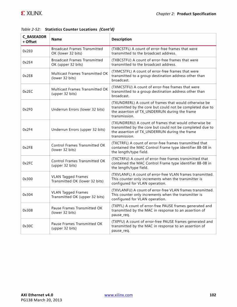
AXI Ethernet v4.0 www.xilinx.com 102PG138 March 20, 2013
Chapter 2: Product Specification
0x2E0 Broadcast Frames Transmitted OK (lower 32 bits)
(TXBCSTFL) A count of error-free frames that were transmitted to the broadcast address.
0x2E4 Broadcast Frames Transmitted OK (upper 32 bits)
(TXBCSTFU) A count of error-free frames that were transmitted to the broadcast address.
0x2E8 Multicast Frames Transmitted OK(lower 32 bits)
(TXMCSTFL) A count of error-free frames that were transmitted to a group destination address other than broadcast.
0x2EC Multicast Frames Transmitted OK(upper 32 bits)
(TXMCSTFU) A count of error-free frames that were transmitted to a group destination address other than broadcast.
0x2F0 Underrun Errors (lower 32 bits)
(TXUNDRERL) A count of frames that would otherwise be transmitted by the core but could not be completed due to the assertion of TX_UNDERRUN during the frame transmission.
0x2F4 Underrun Errors (upper 32 bits)
(TXUNDRERU) A count of frames that would otherwise be transmitted by the core but could not be completed due to the assertion of TX_UNDERRUN during the frame transmission.
0x2F8 Control Frames Transmitted OK(lower 32 bits)
(TXCTRFL) A count of error-free frames transmitted that contained the MAC Control Frame type identif ier 88-08 in the length/type f ield.
0x2FC Control Frames Transmitted OK(upper 32 bits)
(TXCTRFU) A count of error-free frames transmitted that contained the MAC Control Frame type identif ier 88-08 in the length/type f ield.
0x300 VLAN Tagged Frames Transmitted OK (lower 32 bits)
(TXVLANFL) A count of error-free VLAN frames transmitted. This counter only increments when the transmitter is configured for VLAN operation.
0x304 VLAN Tagged Frames Transmitted OK (upper 32 bits)
(TXVLANFU) A count of error-free VLAN frames transmitted. This counter only increments when the transmitter is configured for VLAN operation.
0x308 Pause Frames Transmitted OK(lower 32 bits)
(TXPFL) A count of error-free PAUSE frames generated and transmitted by the MAC in response to an assertion of pause_req.
0x30C Pause Frames Transmitted OK(upper 32 bits)
(TXPFU) A count of error-free PAUSE frames generated and transmitted by the MAC in response to an assertion of pause_req.
Table 2‐52: Statistics Counter Locations (Cont’d)
C_BASEADDR + Offset
Name Description

AXI Ethernet v4.0 www.xilinx.com 103PG138 March 20, 2013
Chapter 2: Product Specification
TEMAC Receive Configuration Word 0 Register ‐ Offset 0x0000_0400
The TEMAC Receive Configuration Word 0 (RCW0) Register is shown in Figure 2-47. This register can be written at any time but the receiver logic only applies the configuration changes during Inter Frame gaps.
Table 2-53 shows the TEMAC Receive Configuration Word 0 Register bit definitions.
TEMAC Receive Configuration Word 1 Register ‐ Offset 0x0000_0404
The TEMAC Receive Configuration Word 1 (RCW1) Register is shown in Figure 2-48. This register can be written at any time but the receiver logic only applies the configuration changes during Inter Frame gaps. The exception to this is the Reset bit which is effective immediately.
Table 2-54 shows the TEMAC Receive Configuration Word1 Register bit definitions.
X-Ref Target - Figure 2-47
Figure 2‐47: TEMAC Receive Configuration Word 0 (RCW0) Register (offset 0x400)
031
PauseAddr(31:0) DS759_18
MS
B
LSB
Table 2‐53: TEMAC Receive Configuration Word 0 (RCW0) Register Bit Definitions
Bits NameCore Access
Reset Value
Description
31 - 0 PauseAddr Read/Write 0xDDCCBBAA
Pause Frame Ethernet MAC Address (31:0): This address is used to match the destination address of any received flow control frames. It is also used as the source address for any transmitted flow control frames.This address is ordered so that the f irst byte transmitted/ received is the lowest position byte in the register. For example, a MAC address of AA-BB-CC-DD-EE-FF would be stored in the PauseAddr(47:0) as 0xFFEED-DCCBBAA.
X-Ref Target - Figure 2-48
Figure 2‐48: TEMAC Receive Configuration Word 1 (RCW1) Register (offset 0x404)
PauseAddr(47:32)ReservedRST FCS VLAN LT_DIS
RXJUM HD CL_DIS
DS759_19
MS
B
LSB
25 24 23 16 15262728293031 0

AXI Ethernet v4.0 www.xilinx.com 104PG138 March 20, 2013
Chapter 2: Product Specification
Table 2‐54: TEMAC Receive Configuration Word1 (RCW1) Register Bit Definitions
Bits NameCore Access
Reset Value
Description
31 RST Read/Write 0
Reset: When this bit is 1, the receiver is reset. The bit automatically resets to 0. The reset also sets all of the receiver configuration registers to their default values. Resetting the receiver without resetting AXI Ethernet core could cause the core to be in an unknown state.0 - no reset1 - initiate a receiver reset
30 JUM(1) Read/Write 1
Jumbo Frame Enable: When this bit is 1 the receiver accepts frames over the maximum length specified in IEEE Std 802.3-2002 specification.0 - receive jumbo frames disabled1 - receive jumbo frames enabled
29 FCS Read/Write 1
In-Band FCS Enable: When this bit is 1, the receiver provides the FCS f ield with the rest of the frame data. When this bit is 0 the FCS f ield is stripped from the receive frame data. In either case the FCS field is verif ied.0 - strip the FCS field from the receive frame data1 - provide the FCS field with the receive frame data
28 RX Read/Write 0
Receive Enable: When this bit is 1, the receiver logic is enabled to operate. When this bit is 0, the receiver ignores activity on the receive interface.0 - receive disabled1 - receive enabled
27 VLAN(2) Read/Write 1
VLAN Frame Enable: When this bit is 1, the receiver accepts VLAN tagged frames. The maximum payload length increases by four bytes.0 - receive of VLAN frames disabled1 - receive of VLAN frames enabled
26 HD Read/Write 0
Half-Duplex Mode: When this bit is 1, the receive operates in half-duplex mode. When this bit is 0, the receiver operates in full-duplex mode. Only full-duplex is supported so this bit should always be set to 0. 0 - full-duplex receive1 - half-duplex receive
25 LT_DIS Read/Write 0
Length/Type Field Valid Check Disable: When this bit is 1, it disables the Length/Type f ield check on the receive frame.0 - perform Length/Type f ield check1 - do not perform Length/Type field check
24 CL_DIS Read/Write 0x0 Control Frame Length Check Disable: When this bit is 1, control frames larger than the minimum frame length can be accepted
23 - 16 Reserved Read 0x0 Reserved: These bits are reserved for future use and always return zero.
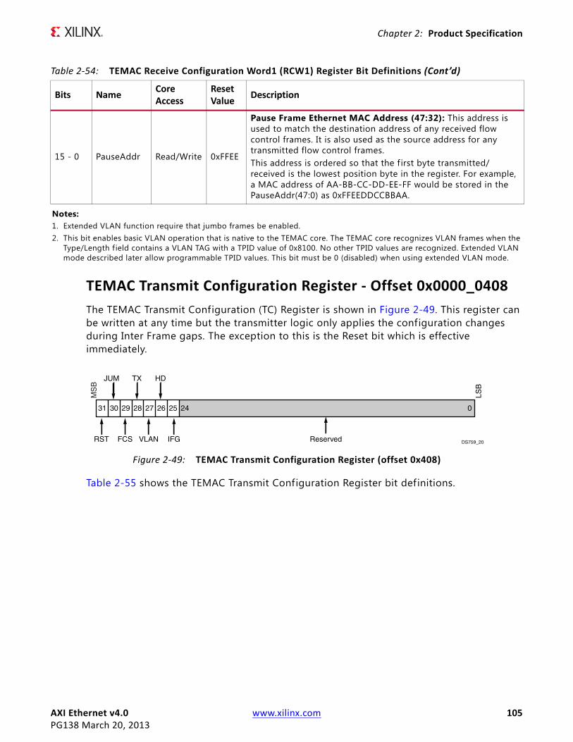
AXI Ethernet v4.0 www.xilinx.com 105PG138 March 20, 2013
Chapter 2: Product Specification
TEMAC Transmit Configuration Register ‐ Offset 0x0000_0408
The TEMAC Transmit Configuration (TC) Register is shown in Figure 2-49. This register can be written at any time but the transmitter logic only applies the configuration changes during Inter Frame gaps. The exception to this is the Reset bit which is effective immediately.
Table 2-55 shows the TEMAC Transmit Configuration Register bit definitions.
15 - 0 PauseAddr Read/Write 0xFFEE
Pause Frame Ethernet MAC Address (47:32): This address is used to match the destination address of any received flow control frames. It is also used as the source address for any transmitted flow control frames.This address is ordered so that the f irst byte transmitted/ received is the lowest position byte in the register. For example, a MAC address of AA-BB-CC-DD-EE-FF would be stored in the PauseAddr(47:0) as 0xFFEEDDCCBBAA.
Notes: 1. Extended VLAN function require that jumbo frames be enabled.2. This bit enables basic VLAN operation that is native to the TEMAC core. The TEMAC core recognizes VLAN frames when the
Type/Length f ield contains a VLAN TAG with a TPID value of 0x8100. No other TPID values are recognized. Extended VLAN mode described later allow programmable TPID values. This bit must be 0 (disabled) when using extended VLAN mode.
Table 2‐54: TEMAC Receive Configuration Word1 (RCW1) Register Bit Definitions (Cont’d)
Bits NameCore Access
Reset Value
Description
X-Ref Target - Figure 2-49
Figure 2‐49: TEMAC Transmit Configuration Register (offset 0x408)
Reserved
JUM
RST FCS VLAN IFG
TX HD
DS759_20
MS
B
LSB
25 24 0262728293031

AXI Ethernet v4.0 www.xilinx.com 106PG138 March 20, 2013
Chapter 2: Product Specification
Table 2‐55: TEMAC Transmit Configuration Register Bit Definitions
Bits NameCoreAccess
ResetValue
Description
31 RST Read/Write 0
Reset: When this bit is 1, the transmitter is reset. The bit automatically resets to 0. The reset also sets all of the transmitter configuration registers to their default values. Resetting the transmitter without resetting AXI Ethernet core could cause the core to be in an unknown state.0 - no reset1 - initiate a transmitter reset
30 JUM(1) Read/Write 1
Jumbo Frame Enable: When this bit is 1 the transmitter sends frames over the maximum length specif ied in IEEE Std 802.3-2002 specification.0 - send jumbo frames disabled1 - send jumbo frames enabled
29 FCS Read/Write 0
In-Band FCS Enable: When this bit is 1, the transmitter accepts the FCS f ield with the rest of the frame data. When this bit is 0 the FCS f ield is calculated and supplied by the transmitter. In either case the FCS f ield is verif ied.0 - transmitter calculates and sends FCS f ield1 - FCS field is provided with transmit frame data
28 TX Read/Write 0
Transmit Enable: When this bit is 1, the transmit logic is enabled to operate. 0 - transmit disabled1 - transmit enabled
27 VLAN(2) Read/Write 1
VLAN Frame Enable: When this bit is 1, the transmitter allows transmission of VLAN tagged frames.0 - transmit of VLAN frames disabled1 - transmit of VLAN frames enabled
26 HD Read/Write 0
Half-Duplex Mode: When this bit is 1, the transmitter operates in half-duplex mode. When this bit is 0, the transmitter operates in full-duplex mode. Only full-duplex is supported so this bit should always be set to 0. 0 - full-duplex transmit1 - half-duplex transmit
25 IFG Read/Write 1
Inter Frame Gap Adjustment Enable: When this bit is 1, the transmitter uses the value of the IFGP register (Figure 2-35) to extend the transmit Inter Frame Gap beyond the minimum of 12 idle cycles (96-bit times on the Ethernet Interface).0 - no IFGP adjustment enabled1 - IFGP adjusted based on IFGP register
24 - 0 Reserved Read 0x0 Reserved: These bits are reserved for future use and always return zero.
Notes: 1. Extended VLAN function require that jumbo frames be enabled.2. This bit enables basic VLAN operation that is native to the TEMAC core. The TEMAC core recognizes VLAN frames when the
Type/Length f ield contains a VLAN TAG with a TPID value of 0x8100. No other TPID values are recognized. Extended VLAN mode described later allow programmable TPID values. This bit must be 0 (disabled) when using extended VLAN mode.

AXI Ethernet v4.0 www.xilinx.com 107PG138 March 20, 2013
Chapter 2: Product Specification
TEMAC Flow Control Configuration Register ‐ Offset 0x0000_040C
The TEMAC Flow Control Configuration (FCC) Register is shown in Figure 2-50. This register can be written at any time but the flow control logic only applies the configuration changes during Inter Frame gaps.
Table 2-56 shows the TEMAC Flow Control Configuration Register bit definitions.
TEMAC Ethernet MAC Mode Configuration Register ‐ Offset 0x0000_0410
The TEMAC Ethernet MAC Mode Configuration (EMMC) Register is shown in Figure 2-51. This register can be written at any time but the Ethernet interface only applies the configuration changes during Inter Frame gaps. This register is slightly different for implementations using the TEMAC (C_TYPE = 0 or C_TYPE = 1).
X-Ref Target - Figure 2-50
Figure 2‐50: TEMAC Flow Control Configuration Register (offset 0x40C)
ReservedReserved
FCTX
FCRXds759_21
MS
B
LSB
293031 28 0
Table 2‐56: TEMAC Flow Control Configuration Register Bit Definitions
Bits NameCore Access
Reset Value
Description
31 Reserved Read 0 Reserved: These bits are reserved for future use and always return zero.
30 FCTX Read/Write 1
Transmit Flow Control Enable: When this bit is 1, the transmitter sends a flow control frame when a value is written to the Transmit Pause Frame Register - Offset 0x0000_0004, page 84.0 - transmit flow control frame disabled1 - transmit flow control frame enabled
29 FCRX Read/Write 1
Receive Flow Control Enable: When this bit is 1, the receive flow control frames inhibit transmitter operation. When this bit is 0, the flow control frames are passed through with other receive frames.0 - receive flow control disabled1 - receive flow control enabled
28 - 0 Reserved Read 0x0 Reserved: These bits are reserved for future use and always return zero.
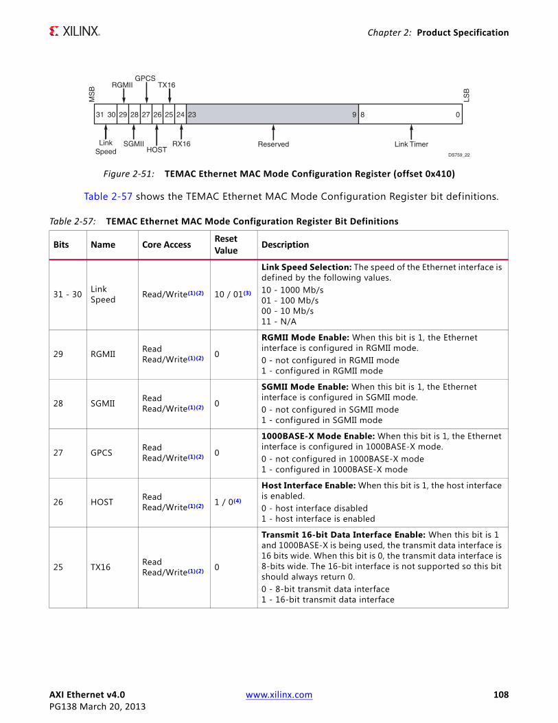
AXI Ethernet v4.0 www.xilinx.com 108PG138 March 20, 2013
Chapter 2: Product Specification
Table 2-57 shows the TEMAC Ethernet MAC Mode Configuration Register bit definitions.
X-Ref Target - Figure 2-51
Figure 2‐51: TEMAC Ethernet MAC Mode Configuration Register (offset 0x410)
Reserved
RGMII
SGMIIHOST
RX16 Link TimerLinkSpeed
GPCSTX16
DS759_22
MS
B
LSB
25 24 23 89 0262728293031
Table 2‐57: TEMAC Ethernet MAC Mode Configuration Register Bit Definitions
Bits Name Core AccessReset Value
Description
31 - 30 Link Speed Read/Write(1)(2) 10 / 01(3)
Link Speed Selection: The speed of the Ethernet interface is defined by the following values.10 - 1000 Mb/s01 - 100 Mb/s00 - 10 Mb/s11 - N/A
29 RGMII ReadRead/Write(1)(2) 0
RGMII Mode Enable: When this bit is 1, the Ethernet interface is configured in RGMII mode.0 - not configured in RGMII mode1 - configured in RGMII mode
28 SGMII ReadRead/Write(1)(2) 0
SGMII Mode Enable: When this bit is 1, the Ethernet interface is configured in SGMII mode.0 - not configured in SGMII mode1 - configured in SGMII mode
27 GPCS ReadRead/Write(1)(2) 0
1000BASE-X Mode Enable: When this bit is 1, the Ethernet interface is configured in 1000BASE-X mode.0 - not configured in 1000BASE-X mode1 - configured in 1000BASE-X mode
26 HOST ReadRead/Write(1)(2) 1 / 0(4)
Host Interface Enable: When this bit is 1, the host interface is enabled. 0 - host interface disabled1 - host interface is enabled
25 TX16 ReadRead/Write(1)(2) 0
Transmit 16-bit Data Interface Enable: When this bit is 1 and 1000BASE-X is being used, the transmit data interface is 16 bits wide. When this bit is 0, the transmit data interface is 8-bits wide. The 16-bit interface is not supported so this bit should always return 0.0 - 8-bit transmit data interface1 - 16-bit transmit data interface

AXI Ethernet v4.0 www.xilinx.com 109PG138 March 20, 2013
Chapter 2: Product Specification
24 RX16 ReadRead/Write(1)(2) 0
Receive 16-bit Data Interface Enable: When this bit is 1 and 1000BASE-X is being used, the receive data interface is 16 bits wide. When this bit is 0, the receive data interface is 8-bits wide. The 16-bit interface is not supported so this bit should always return 0.0 - 8-bit receive data interface1 - 16-bit receive data interface
23-9 Reserved Read 0x0 Reserved: These bits are reserved for future use and always return zero.
8-0 Link Timer Read/Write(1)(2) Link Timer: Sets the programmable link timer value, for operation with 1000BASE-X or SGMII modes
Notes: 1. Only bits 31-30 are Read/Write accessible in the TEMAC configuration2. Only bits 31-30 are used with TEMAC. All other bits are reserved.3. The Reset Value for LINK SPEED is “10” or 1000 Mb/s for all PHY interfaces except for MII which is not capable of that speed.
The Reset Value for LINK SPEED for the MII interface is “01” or 100 Mb/s.4. The use of the Host interface is hidden from you and is of no concern. However, this register returns a different reset value
for different TEMAC implementations. The TEMAC implementation returns a 0.
Table 2‐57: TEMAC Ethernet MAC Mode Configuration Register Bit Definitions (Cont’d)
Bits Name Core AccessReset Value
Description

AXI Ethernet v4.0 www.xilinx.com 110PG138 March 20, 2013
Chapter 2: Product Specification
Receive Max Frame Configuration Register ‐ Offset 0x00000414
The Receive Max Frame Configuration (RXFC) Register is shown in Figure 2-52. This register applies only to the TEMAC.
Table 2-58 shows the Receive Max Frame Configuration Register bit definitions. This register applies only to the TEMAC.
X-Ref Target - Figure 2-52
Figure 2‐52: Receive Max Frame Configuration Register (offset 0x00000414)
Reserved
Max Frame Length
DS759_23
MS
B
LSB
17 1631 015 14
En
Reserved
Table 2‐58: Receive Max Frame Configuration Register Bit Definitions
Bits NameCore Access
Reset Value
Description
31 - 17 Reserved Read 0 Reserved. These bits are reserved for future use and always return zero.
16 Enable Read/Write 0
RX Max Frame Enable. When low the MAC assumes use of the standard 1518/1522 depending upon the setting of VLAN Frame Enable in Table 2-54. When High the MAC allows frames up to RX Max Frame Length irrespective of the value of VLAN Frame Enable. If Jumbo Frame Enable is set in Table 2-54 then this register has no effect.
15 Reserved Read 0 Reserved. These bits are reserved for future use and always return zero.
14 - 0 Max Frame Length Read/Write 0x7D0 RX Max Frame Length: Set to preferred MAX frame length.
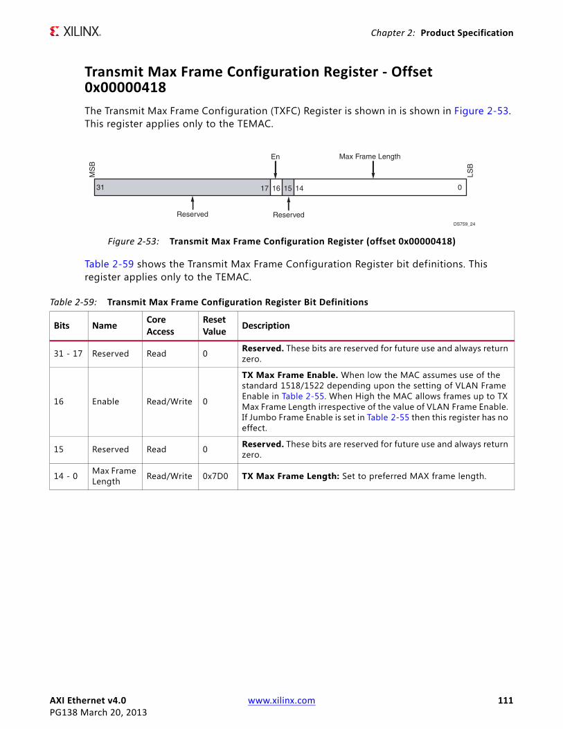
AXI Ethernet v4.0 www.xilinx.com 111PG138 March 20, 2013
Chapter 2: Product Specification
Transmit Max Frame Configuration Register ‐ Offset 0x00000418
The Transmit Max Frame Configuration (TXFC) Register is shown in is shown in Figure 2-53. This register applies only to the TEMAC.
Table 2-59 shows the Transmit Max Frame Configuration Register bit definitions. This register applies only to the TEMAC.
X-Ref Target - Figure 2-53
Figure 2‐53: Transmit Max Frame Configuration Register (offset 0x00000418)
Reserved
Max Frame Length
DS759_24
MS
B
LSB
17 1631 015 14
En
Reserved
Table 2‐59: Transmit Max Frame Configuration Register Bit Definitions
Bits NameCore Access
Reset Value
Description
31 - 17 Reserved Read 0 Reserved. These bits are reserved for future use and always return zero.
16 Enable Read/Write 0
TX Max Frame Enable. When low the MAC assumes use of the standard 1518/1522 depending upon the setting of VLAN Frame Enable in Table 2-55. When High the MAC allows frames up to TX Max Frame Length irrespective of the value of VLAN Frame Enable. If Jumbo Frame Enable is set in Table 2-55 then this register has no effect.
15 Reserved Read 0 Reserved. These bits are reserved for future use and always return zero.
14 - 0 Max Frame Length Read/Write 0x7D0 TX Max Frame Length: Set to preferred MAX frame length.
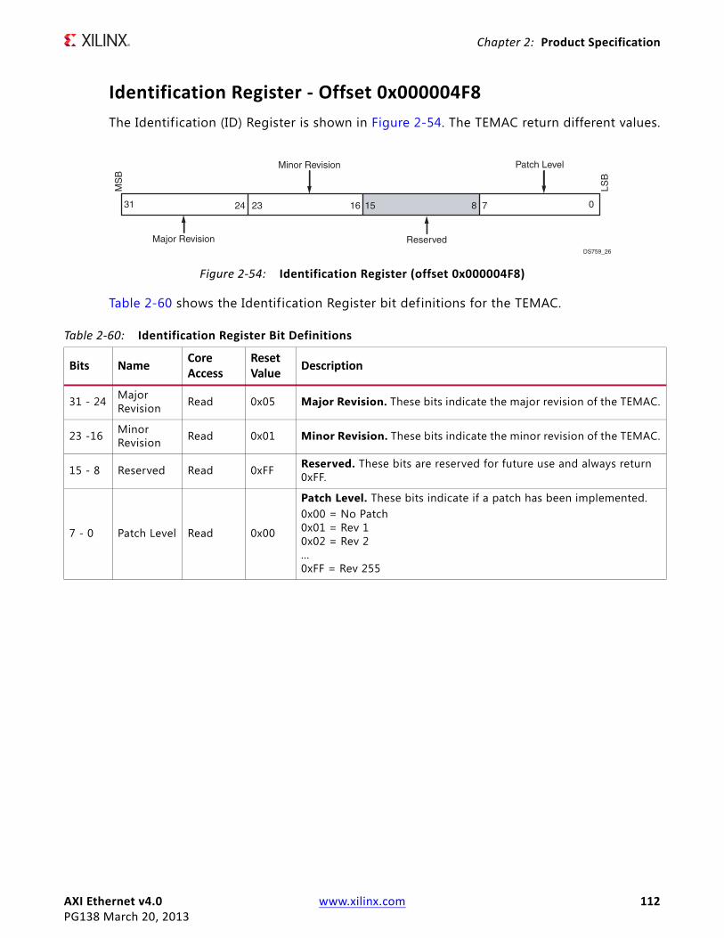
AXI Ethernet v4.0 www.xilinx.com 112PG138 March 20, 2013
Chapter 2: Product Specification
Identification Register ‐ Offset 0x000004F8
The Identif ication (ID) Register is shown in Figure 2-54. The TEMAC return different values.
Table 2-60 shows the Identif ication Register bit definitions for the TEMAC.
X-Ref Target - Figure 2-54
Figure 2‐54: Identification Register (offset 0x000004F8)
Major Revision
Patch Level
DS759_26
MS
B
LSB
1631 015
Minor Revision
Reserved
24 23 8 7
Table 2‐60: Identification Register Bit Definitions
Bits NameCore Access
Reset Value
Description
31 - 24 Major Revision Read 0x05 Major Revision. These bits indicate the major revision of the TEMAC.
23 -16 Minor Revision Read 0x01 Minor Revision. These bits indicate the minor revision of the TEMAC.
15 - 8 Reserved Read 0xFF Reserved. These bits are reserved for future use and always return 0xFF.
7 - 0 Patch Level Read 0x00
Patch Level. These bits indicate if a patch has been implemented.0x00 = No Patch0x01 = Rev 10x02 = Rev 2...0xFF = Rev 255
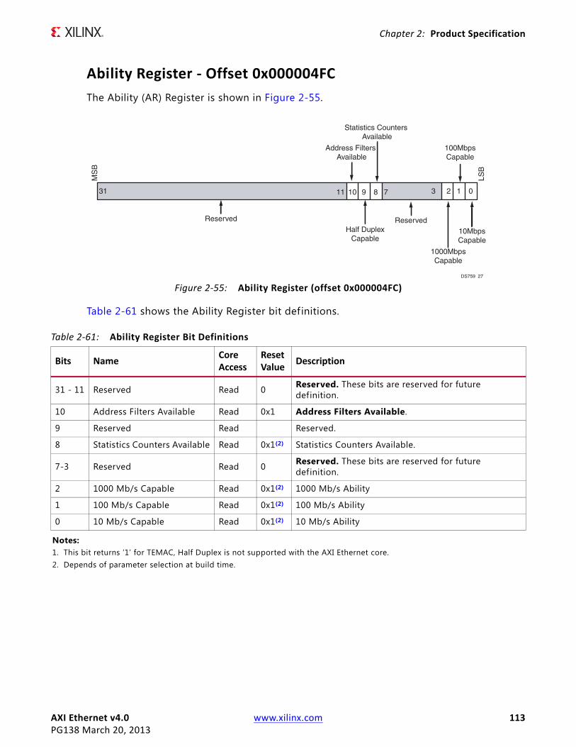
AXI Ethernet v4.0 www.xilinx.com 113PG138 March 20, 2013
Chapter 2: Product Specification
Ability Register ‐ Offset 0x000004FC
The Ability (AR) Register is shown in Figure 2-55.
Table 2-61 shows the Ability Register bit definitions.
X-Ref Target - Figure 2-55
Figure 2‐55: Ability Register (offset 0x000004FC)
Reserved
1000MbpsCapable
10MbpsCapable
100MbpsCapable
DS759_27
MS
B
LSB
31 01237891011
Reserved
Address Filters Available
Half DuplexCapable
Statistics Counters Available
Table 2‐61: Ability Register Bit Definitions
Bits NameCoreAccess
ResetValue
Description
31 - 11 Reserved Read 0 Reserved. These bits are reserved for future definition.
10 Address Filters Available Read 0x1 Address Filters Available.
9 Reserved Read Reserved.
8 Statistics Counters Available Read 0x1(2) Statistics Counters Available.
7-3 Reserved Read 0 Reserved. These bits are reserved for future definition.
2 1000 Mb/s Capable Read 0x1(2) 1000 Mb/s Ability
1 100 Mb/s Capable Read 0x1(2) 100 Mb/s Ability
0 10 Mb/s Capable Read 0x1(2) 10 Mb/s Ability
Notes: 1. This bit returns ‘1’ for TEMAC, Half Duplex is not supported with the AXI Ethernet core.2. Depends of parameter selection at build time.

AXI Ethernet v4.0 www.xilinx.com 114PG138 March 20, 2013
Chapter 2: Product Specification
MII Management Configuration Register ‐ Offset 0x0000_0500
The MII Management (MDIO) Configuration (MC) Register is shown in Figure 2-56. This register provides control for the TEMAC PHY MII management (MDIO) interface. The MDIO interface supplies a clock to the external device, MDC. This clock is derived from the HostClk input signal using the value in the Clock Divide[5:0]. The frequency of the MDIO clock is given by the following equation:
To comply with the IEEE 802.3-2002 specif ication for this interface, the frequency of the MDC should not exceed 2.5 MHz. To prevent MDC from being out of specification, the Clock Divide[5:0] value powers up at 000000. While this value is in the register, it is impossible to enable the MDIO interface. Even if the MDIO interface is enabled by setting bit 6 of this register, the MDIO port is still disabled until a non-zero value has been written into the clock divide field.
Table 2-62 shows the MII Management Configuration Register bit definitions.
fMDC
fHOSTCLK1 Clock Divide[5:0]+ 2
----------------------------------------------------------------------=
X-Ref Target - Figure 2-56
Figure 2‐56: MII Management (MDIO) Configuration Register (offset 0x500)
Reserved
CLOCKDIVIDE
MDIOENDS759_28
MS
B
LSB
06731 5
Table 2‐62: MDIO MC Register Bit Definitions
Bits NameCoreAccess
ResetValue
Description
31-7 Reserved Read 0x0 Reserved: These bits are reserved for future use and always return zero.
6 MDIOEN Read/Write 0
MDIO Enable: When this bit is 1, the MDIO (MII Management) interface is used to access the PHY.0 - MDIO disabled1 - MDIO enabled
5 - 0 CLOCK DIVIDE Read/Write 0x0
Clock Divide: This value is used to derive the MDC (MII Management interface clock) signal. The maximum permitted frequency is 2.5 MHz.

AXI Ethernet v4.0 www.xilinx.com 115PG138 March 20, 2013
Chapter 2: Product Specification
MII Management Control Register ‐ Offset 0x0000_0504
The MII Management (MDIO) Control Register (MCR) is shown in Figure 2-57. This register can be written at any time but the Ethernet interface only applies the configuration changes during Inter Frame gaps. This register is slightly different for implementations using the TEMAC (C_TYPE = 0 or C_TYPE = 1).
Table 2-63 shows the MII Management Control Register bit definitions.
X-Ref Target - Figure 2-57
Figure 2‐57: MII Management (MDIO) Control Register (offset 0x504)
PHYAD REGAD
Reserved Reserved OP Initiate RDY
Reserved Reserved Reserved
DS759_29
MS
B
LSB
242829 23 21 20 1516 14 13 12 11 10 8 7 6 031
Table 2‐63: MDIO MCR Bit Definitions
Bits Name Core AccessReset Value
Description
31 - 29 Reserved Reserved 000 Reserved
28-24 PHYAD Read/Write 00000 PHY Physical Address: The physical address of the PHY.
23-21 Reserved Reserved 000 Reserved
20-16 REGAD Read/Write(1) 00000 PHY Register Address: These bits represent the register to be accessed in a particular PHY, as indicated in the PHYAD field.
15-14 OP Read/Write 00
Operation Code. These bits determine if a read or write is going to be performed.01 - Write10 - Read
13-12 Reserved Read/Write 00 Reserved
11 Initiate Read/Write(2) 0Initiate: This bit must be set to 1 to initiate a MDIO transaction. 0 = Do not start an MDIO transaction1 = Initiate an MDIO transaction
10-8 Reserved Read/Write 000 Reserved
7 RDY Read 1
Ready: This bit indicates if the MII Management interface is ready to accept a new transaction.0 = Cannot accept a new transaction1 = Ready to accept a new transaction
6-0 Reserved Reserved 0000000 Reserved
Notes: 1. The f irst 16 registers (0-15) are defined by IEEE Std 802.3-2005. The remaining 16 registers (16-31) are reserved for PHY
vendors’ own register definition.2. This bit clears upon a write.

AXI Ethernet v4.0 www.xilinx.com 116PG138 March 20, 2013
Chapter 2: Product Specification
MII Management Write Data Register ‐ Offset 0x0000_0508
The MII Management (MDIO) Write Data Register (MWD) is shown in Figure 2-58. This register is a temporary storage location for data to be written to a PHY register (internal or external) through the MDIO interface. A MDIO write is initiated by writing to the MII Management Control Register with the physical PHY address (PHYAD), the PHY register to be accessed (REGAD), the access type, and setting the Initiate bit after providing the data to this register.
This register is only used for writing to PHY registers. When reading from PHY registers, the data is stored in the MII Management Read Data Register. For more information on using the MDIO interface for accessing PHY registers, see Using the Address Filters, page 22.
Table 2-64 shows the MII Management Write Data Register bit definitions.
X-Ref Target - Figure 2-58
Figure 2‐58: MII Management (MDIO) Write Data Register (offset 0x508)
MiimWrDataReservedDS759_30
MS
B
LSB
15 031 16
Table 2‐64: MWD Register Bit Definitions
Bits NameCoreAccess
ResetValue
Description
31 - 16 Reserved Read 0x0 Reserved: These bits are reserved for future use and always return zero.
15 - 0 Write Data Read/Write 0x0 MII Management Write Data: This f ield temporarily holds data to be written to a PHY register.
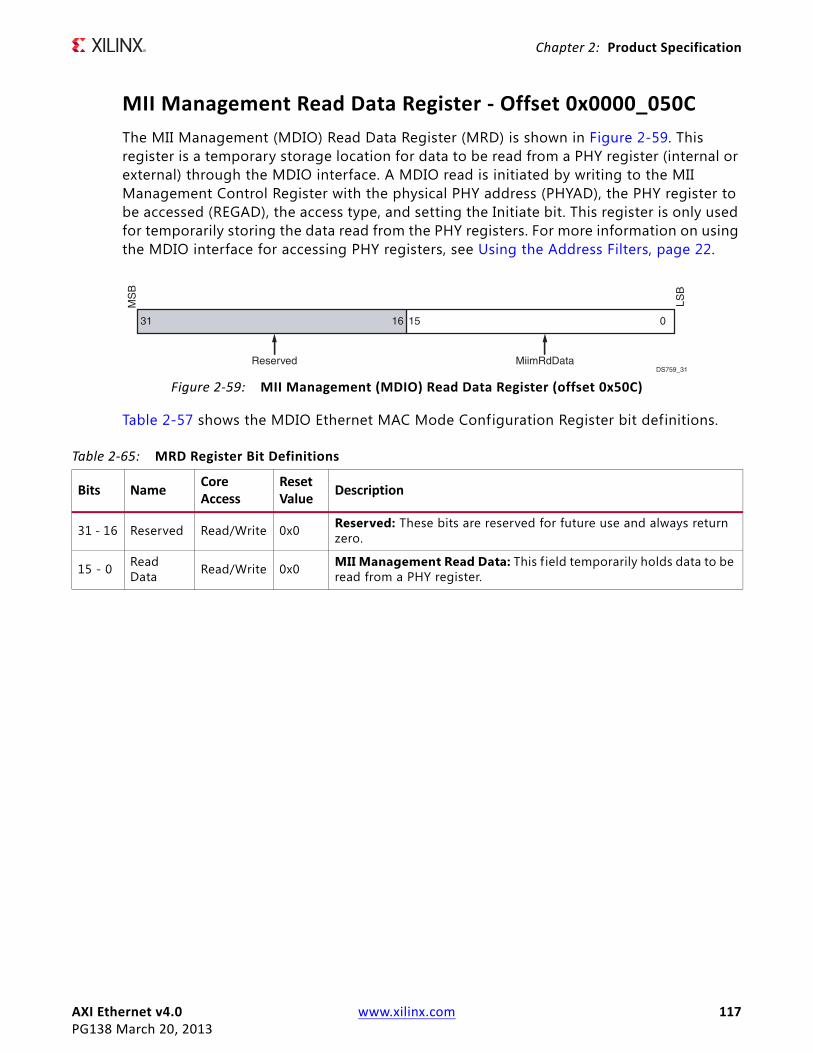
AXI Ethernet v4.0 www.xilinx.com 117PG138 March 20, 2013
Chapter 2: Product Specification
MII Management Read Data Register ‐ Offset 0x0000_050C
The MII Management (MDIO) Read Data Register (MRD) is shown in Figure 2-59. This register is a temporary storage location for data to be read from a PHY register (internal or external) through the MDIO interface. A MDIO read is initiated by writing to the MII Management Control Register with the physical PHY address (PHYAD), the PHY register to be accessed (REGAD), the access type, and setting the Initiate bit. This register is only used for temporarily storing the data read from the PHY registers. For more information on using the MDIO interface for accessing PHY registers, see Using the Address Filters, page 22.
Table 2-57 shows the MDIO Ethernet MAC Mode Configuration Register bit definitions.
X-Ref Target - Figure 2-59
Figure 2‐59: MII Management (MDIO) Read Data Register (offset 0x50C)
MiimRdDataReservedDS759_31
MS
B
LSB
15 031 16
Table 2‐65: MRD Register Bit Definitions
Bits NameCore Access
Reset Value
Description
31 - 16 Reserved Read/Write 0x0 Reserved: These bits are reserved for future use and always return zero.
15 - 0 Read Data Read/Write 0x0 MII Management Read Data: This f ield temporarily holds data to be
read from a PHY register.
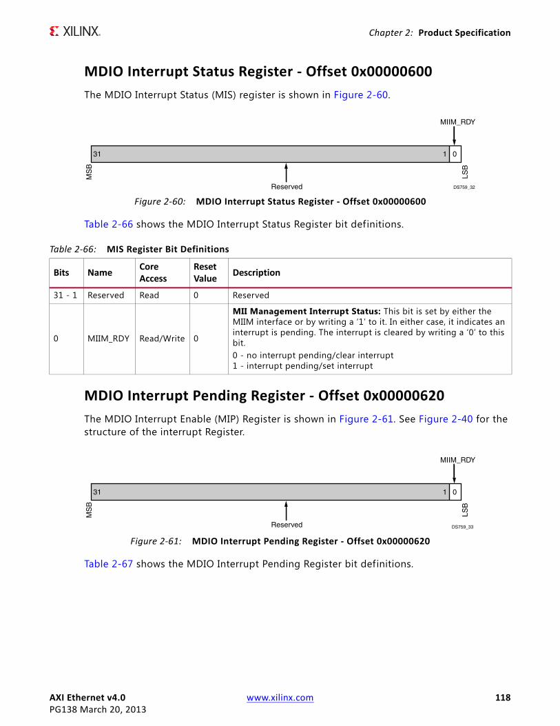
AXI Ethernet v4.0 www.xilinx.com 118PG138 March 20, 2013
Chapter 2: Product Specification
MDIO Interrupt Status Register ‐ Offset 0x00000600
The MDIO Interrupt Status (MIS) register is shown in Figure 2-60.
Table 2-66 shows the MDIO Interrupt Status Register bit definitions.
MDIO Interrupt Pending Register ‐ Offset 0x00000620
The MDIO Interrupt Enable (MIP) Register is shown in Figure 2-61. See Figure 2-40 for the structure of the interrupt Register.
Table 2-67 shows the MDIO Interrupt Pending Register bit definitions.
X-Ref Target - Figure 2-60
Figure 2‐60: MDIO Interrupt Status Register ‐ Offset 0x00000600
31 1 0
Reserved
MIIM_RDY
DS759_32
MS
B
LSB
Table 2‐66: MIS Register Bit Definitions
Bits NameCore Access
Reset Value
Description
31 - 1 Reserved Read 0 Reserved
0 MIIM_RDY Read/Write 0
MII Management Interrupt Status: This bit is set by either the MIIM interface or by writing a ‘1’ to it. In either case, it indicates an interrupt is pending. The interrupt is cleared by writing a ‘0’ to this bit.0 - no interrupt pending/clear interrupt1 - interrupt pending/set interrupt
X-Ref Target - Figure 2-61
Figure 2‐61: MDIO Interrupt Pending Register ‐ Offset 0x00000620
31 1 0
Reserved
MIIM_RDY
DS759_33
MS
B
LSB

AXI Ethernet v4.0 www.xilinx.com 119PG138 March 20, 2013
Chapter 2: Product Specification
MDIO Interrupt Enable Register ‐ Offset 0x00000640
The MDIO Interrupt Enable (MIE) Register is shown in Figure 2-62. See Figure 2-37 for the structure of the interrupt register.
Table 2-68 shows the MDIO Interrupt Enable Register bit definitions.
Table 2‐67: MIP Register Bit Definitions
Bits NameCore Access
Reset Value
Description
31 - 1 Reserved Read 0 Reserved
0 MIIM_RDY Read 0
MII Management Interrupt Pending: This bit indicates an interrupt is pending if the corresponding bit in the MIS and MIE are set.0 - no interrupt pending1 - interrupt pending
X-Ref Target - Figure 2-62
Figure 2‐62: MDIO Interrupt Enable Register ‐ Offset 0x00000640
31 1 0
Reserved
MIIM_RDY
DS759_34
MS
B
LSB
Table 2‐68: MIE Register Bit Definitions
Bits NameCore Access
Reset Value
Description
31 - 1 Reserved Read 0 Reserved
0 MIIM_RDY Read/Write 0
MII Management Interrupt Enable: When set, this bit allows an interrupt in the MIS register to generate an interrupt in the MIP register.0 - Disable interrupt1 - Enable interrupt
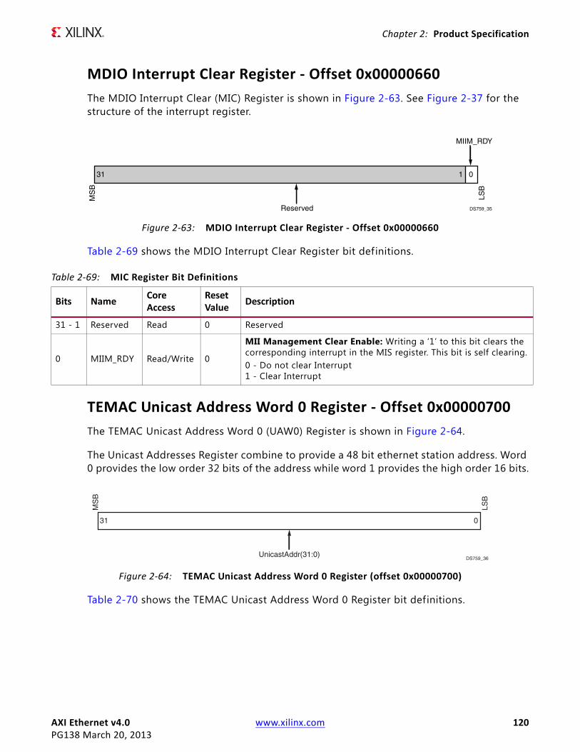
AXI Ethernet v4.0 www.xilinx.com 120PG138 March 20, 2013
Chapter 2: Product Specification
MDIO Interrupt Clear Register ‐ Offset 0x00000660
The MDIO Interrupt Clear (MIC) Register is shown in Figure 2-63. See Figure 2-37 for the structure of the interrupt register.
Table 2-69 shows the MDIO Interrupt Clear Register bit definitions.
TEMAC Unicast Address Word 0 Register ‐ Offset 0x00000700
The TEMAC Unicast Address Word 0 (UAW0) Register is shown in Figure 2-64.
The Unicast Addresses Register combine to provide a 48 bit ethernet station address. Word 0 provides the low order 32 bits of the address while word 1 provides the high order 16 bits.
Table 2-70 shows the TEMAC Unicast Address Word 0 Register bit definitions.
X-Ref Target - Figure 2-63
Figure 2‐63: MDIO Interrupt Clear Register ‐ Offset 0x00000660
31 1 0
Reserved
MIIM_RDY
DS759_35
MS
B
LSB
Table 2‐69: MIC Register Bit Definitions
Bits NameCore Access
Reset Value
Description
31 - 1 Reserved Read 0 Reserved
0 MIIM_RDY Read/Write 0
MII Management Clear Enable: Writing a ‘1’ to this bit clears the corresponding interrupt in the MIS register. This bit is self clearing.0 - Do not clear Interrupt1 - Clear Interrupt
X-Ref Target - Figure 2-64
Figure 2‐64: TEMAC Unicast Address Word 0 Register (offset 0x00000700)
031
UnicastAddr(31:0)DS759_36
MS
B
LSB
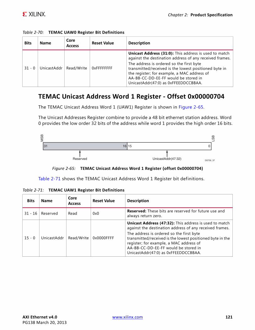
AXI Ethernet v4.0 www.xilinx.com 121PG138 March 20, 2013
Chapter 2: Product Specification
TEMAC Unicast Address Word 1 Register ‐ Offset 0x00000704
The TEMAC Unicast Address Word 1 (UAW1) Register is shown in Figure 2-65.
The Unicast Addresses Register combine to provide a 48 bit ethernet station address. Word 0 provides the low order 32 bits of the address while word 1 provides the high order 16 bits.
Table 2-71 shows the TEMAC Unicast Address Word 1 Register bit definitions.
Table 2‐70: TEMAC UAW0 Register Bit Definitions
Bits NameCore Access
Reset Value Description
31 - 0 UnicastAddr Read/Write 0xFFFFFFFF
Unicast Address (31:0): This address is used to match against the destination address of any received frames.The address is ordered so the f irst byte transmitted/received is the lowest positioned byte in the register; for example, a MAC address of AA-BB-CC-DD-EE-FF would be stored in UnicastAddr(47:0) as 0xFFEEDDCCBBAA.
X-Ref Target - Figure 2-65
Figure 2‐65: TEMAC Unicast Address Word 1 Register (offset 0x00000704)
UnicastAddr(47:32)ReservedDS759_37
MS
B
LSB
15 031 16
Table 2‐71: TEMAC UAW1 Register Bit Definitions
Bits NameCore Access
Reset Value Description
31 - 16 Reserved Read 0x0 Reserved: These bits are reserved for future use and always return zero.
15 - 0 UnicastAddr Read/Write 0x0000FFFF
Unicast Address (47:32): This address is used to match against the destination address of any received frames.The address is ordered so the first byte transmitted/received is the lowest positioned byte in the register; for example, a MAC address of AA-BB-CC-DD-EE-FF would be stored in UnicastAddr(47:0) as 0xFFEEDDCCBBAA.

AXI Ethernet v4.0 www.xilinx.com 122PG138 March 20, 2013
Chapter 2: Product Specification
Filter Mask Index Register ‐ Offset 0x00000708
The TEMAC Address Filter Mode (FMI) Register is shown in Figure 2-66.
Table 2-72 shows the TEMAC Address Filter Mask Register bit definitions.
Address Filter Register 0 (31:0)‐ Offset 0x00000710
This register can be used to f ilter any address type, not just multicast addresses. Before accessing this register, set the Filter Mask Index (FM_IND) to the appropriate setting. See Using the Address Filters, page 22 for more information.
X-Ref Target - Figure 2-66
Figure 2‐66: Filter Mask Index Register (offset 0x00000708)
DS759_38
MS
B
LSB
Reserved FM_INDPM
30 8 7 031
Table 2‐72: FMI Register Bit Definitions
Bits NameCoreAccess
ResetValue
Description
31 PM(1) Read/Write 1
Promiscuous Receive Address Mode Enable: When this bit is 1, the receive address filtering is disabled and all destination addresses are accepted. 0 - address f iltering enabled1 - address f iltering disabled (all addresses accepted)
30 - 8 Reserved Read 0x0 Reserved: These bits are reserved for future definition and always return zero.
7 - 0 FM_IND Read/Write 0x00
Filter Mask Index: Provides the address index for the f ilter table. When set, it does not need to be changed until another address f ilter entry needs accessed.0x00 = Filter 00x01 = Filter 10x02 = Filter 20x03 = Filter 3
Notes: 1. Extended Multicast Filtering requires that the promiscuous mode be enabled/ address f iltering is disabled.
X-Ref Target - Figure 2-67
Figure 2‐67: Address Filter Register 0

AXI Ethernet v4.0 www.xilinx.com 123PG138 March 20, 2013
Chapter 2: Product Specification
Table 2-73 shows the Address Filter 0 (AF0) Register bit definitions.
Address Filter Register 1 (47:32) ‐ Offset 0x00000714
This register can be used to f ilter any address type, not just multicast addresses. Before accessing this register, set the Filter Mask Index (FM_IND) to the appropriate setting. See Using the Address Filters, page 22 for more information.
Table 2-74 shows the Address Filter 1 (AF1) Register bit definitions.
To update an address f ilter, f irst select the address f ilter to be accessed (bottom bits of the Filter Mask Index Register (the MSB of this register provides the Promiscuous mode control), then access the associated register.
Table 2‐73: AF0 Bit Definitions
Bits Name Core AccessReset Value
Description
31 - 0AddressFilter (31:0)
Read/Write 0xFFFFFFFF
Address Filter (31:0): This address is used to match against the destination address of any received frames. The address is ordered so the f irst byte transmitted/received is the lowest positioned byte in the register; for example, a MAC address of AA-BB-CC-DD-EE-FF would be stored in Addr(47:0) as 0xFFEEDDCCBBAA.
X-Ref Target - Figure 2-68
Figure 2‐68: Address Filter Register 1
Table 2‐74: AF1 Register Bit Definitions
Bits NameCoreAccess
Reset Value
Description
31 - 16 Reserved Read 0x0000
Reserved: These bits are reserved for future definition and always return zero.
15 - 0 Address Filter (47:32) Read/Write 0xFFFF
Address Filter(47:32): This address is used to match against the destination address of any received frames. The address is ordered so the f irst byte transmitted/received is the lowest positioned byte in the register; for example, a MAC address of AA-BB-CC-DD-EE-FF would be stored in Addr(47:0) as 0xFFEEDDCCBBAA.

AXI Ethernet v4.0 www.xilinx.com 124PG138 March 20, 2013
Chapter 2: Product Specification
Transmit VLAN Data Table ‐ Offset 0x0000_4000‐0x0000_7FFF
This table is used for data to support transmit VLAN tagging, VLAN stripping, and VLAN translation. The table is always 4K entries deep but the width depends on how many of the VLAN functions are included at build time. VLAN translation requires 12 bits at each location while VLAN stripping and VLAN tagging require 1 bit each at each location. When all transmit VLAN functions are included, the table is 14 bits wide. If VLAN functions are not included, the bits for those functions are not present and writes to those bits have no effect while reads return zero.
IMPORTANT: The table can be either 1-bit, 2-bits, 12-bits, 13-bits, or 14-bits wide depending on which features are present. The table must be initialized by software through the AXI4-Lite and is addressed on 32-bit word boundaries.
The transmit VLAN Table entry with all VLAN functions present is shown in Figure 2-69 while Figure 2-70 shows the transmit VLAN Table entry with only the translation f ield. The bit locations for the functions do not change even when some functions are not used in the build. See Extended VLAN Support for more details.
X-Ref Target - Figure 2-69
Figure 2‐69: Transmit VLAN Table Entry with all Fields (offset 0x0000_4000‐0x0000_7FFF)
31 1314 2 01
Reserved StrpEnbl
TagEnblDS759_41
TransVlanVid
MS
B
LSB
X-Ref Target - Figure 2-70
Figure 2‐70: Transmit VLAN Table Entry with One Field (offset 0x0000_4000‐0x0000_7FFF)
31 1314 2 01
Reserved Reserved
ReservedDS759_42
TransVlanVid
MS
B
LSB
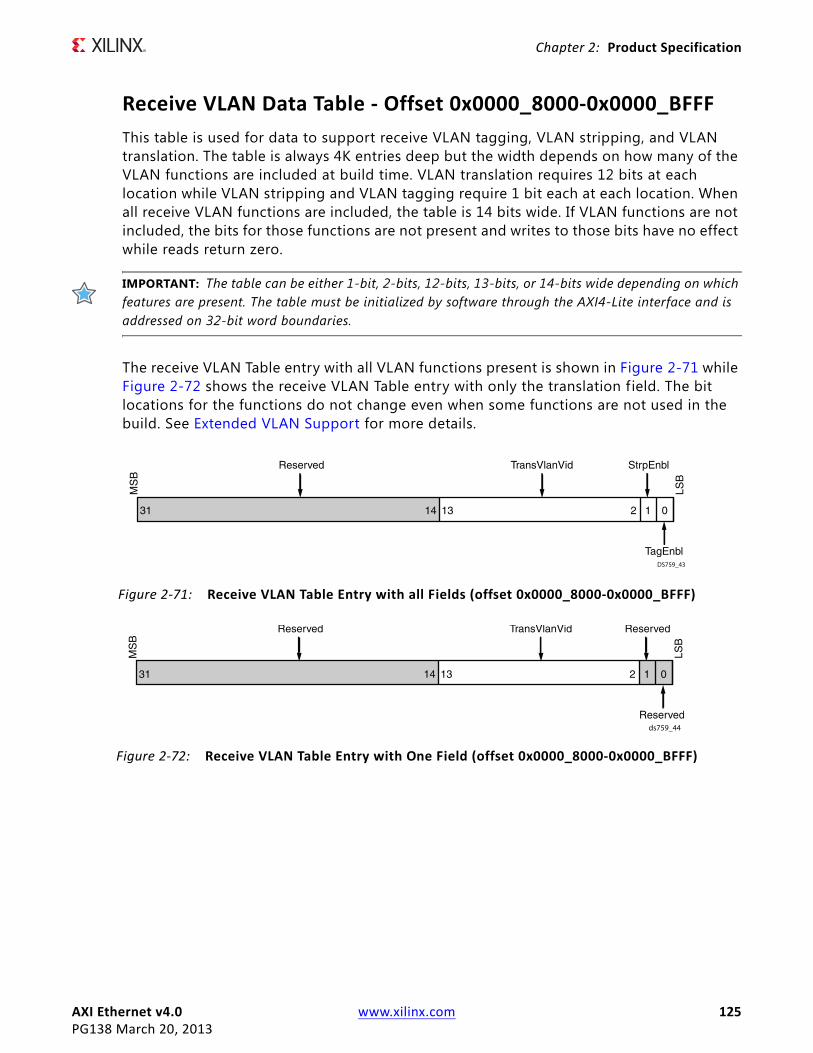
AXI Ethernet v4.0 www.xilinx.com 125PG138 March 20, 2013
Chapter 2: Product Specification
Receive VLAN Data Table ‐ Offset 0x0000_8000‐0x0000_BFFF
This table is used for data to support receive VLAN tagging, VLAN stripping, and VLAN translation. The table is always 4K entries deep but the width depends on how many of the VLAN functions are included at build time. VLAN translation requires 12 bits at each location while VLAN stripping and VLAN tagging require 1 bit each at each location. When all receive VLAN functions are included, the table is 14 bits wide. If VLAN functions are not included, the bits for those functions are not present and writes to those bits have no effect while reads return zero.
IMPORTANT: The table can be either 1-bit, 2-bits, 12-bits, 13-bits, or 14-bits wide depending on which features are present. The table must be initialized by software through the AXI4-Lite interface and is addressed on 32-bit word boundaries.
The receive VLAN Table entry with all VLAN functions present is shown in Figure 2-71 while Figure 2-72 shows the receive VLAN Table entry with only the translation f ield. The bit locations for the functions do not change even when some functions are not used in the build. See Extended VLAN Support for more details.
X-Ref Target - Figure 2-71
Figure 2‐71: Receive VLAN Table Entry with all Fields (offset 0x0000_8000‐0x0000_BFFF)
31 1314 2 01
Reserved StrpEnbl
TagEnblDS759_43
TransVlanVid
MS
B
LSB
X-Ref Target - Figure 2-72
Figure 2‐72: Receive VLAN Table Entry with One Field (offset 0x0000_8000‐0x0000_BFFF)
31 1314 2 01
Reserved Reserved
Reserved
TransVlanVid
MS
B
LSB
ds759_44

AXI Ethernet v4.0 www.xilinx.com 126PG138 March 20, 2013
Chapter 2: Product Specification
AVB Addressing
Receive PTP Packet Buffer ‐ Offset 0x00010000 ‐ 0x00010FFF
The Receive PTP Packet Buffer is 4 kb. See the version of the Tri-Mode Ethernet MAC core listed in the change log for more information.
Transmit PTP Packet Buffer ‐ Offset 0x00011000 ‐ 0x000117FF
The Transmit PTP Packet Buffer is divided into eight identical buffer sections with each section containing 256 bytes. See the version of the Tri-Mode Ethernet MAC core listed in the change log for more information.
AVB Tx/Rx Configuration ‐ Offset 0x00012000 ‐ 0x0001201B
See the version of the Tri-Mode Ethernet MAC core listed in the change log for more information.
AVB RTC Configuration ‐ Offset 0x00012800 ‐ 0x000128FF
See the version of the Tri-Mode Ethernet MAC core listed in the change log for more information.
Multicast Address Table ‐ Offset 0x0002_0000‐0x0003_FFFF
The Multicast Address Table entry is shown in Figure 2-74. The multicast address table is only present when extended multicast address f iltering is selected at build-time (C_MCAST_EXTEND = 1). The purpose of the table is to allow the AXI Ethernet core to support reception of frames addressed to many multicast addresses while providing some of the filtering in hardware to off load some of the overhead required for f iltering in software.
While a MAC multicast address is defined as any 48 bit MAC address that has bit 0 (LSB) set to 1 (for example 01:00:00:00:00:00), in most cases the MAC multicast address is created from a IP multicast address as shown in Figure 2-73.
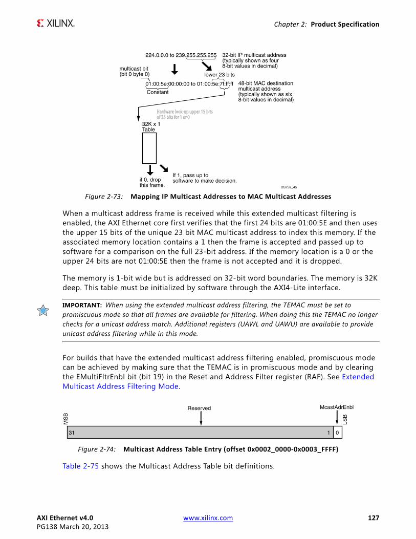
AXI Ethernet v4.0 www.xilinx.com 127PG138 March 20, 2013
Chapter 2: Product Specification
When a multicast address frame is received while this extended multicast f iltering is enabled, the AXI Ethernet core f irst verif ies that the f irst 24 bits are 01:00:5E and then uses the upper 15 bits of the unique 23 bit MAC multicast address to index this memory. If the associated memory location contains a 1 then the frame is accepted and passed up to software for a comparison on the full 23-bit address. If the memory location is a 0 or the upper 24 bits are not 01:00:5E then the frame is not accepted and it is dropped.
The memory is 1-bit wide but is addressed on 32-bit word boundaries. The memory is 32K deep. This table must be initialized by software through the AXI4-Lite interface.
IMPORTANT: When using the extended multicast address filtering, the TEMAC must be set to promiscuous mode so that all frames are available for filtering. When doing this the TEMAC no longer checks for a unicast address match. Additional registers (UAWL and UAWU) are available to provide unicast address filtering while in this mode.
For builds that have the extended multicast address f iltering enabled, promiscuous mode can be achieved by making sure that the TEMAC is in promiscuous mode and by clearing the EMultiFltrEnbl bit (bit 19) in the Reset and Address Filter register (RAF). See Extended Multicast Address Filtering Mode.
Table 2-75 shows the Multicast Address Table bit definitions.
X-Ref Target - Figure 2-73
Figure 2‐73: Mapping IP Multicast Addresses to MAC Multicast Addresses
X-Ref Target - Figure 2-74
Figure 2‐74: Multicast Address Table Entry (offset 0x0002_0000‐0x0003_FFFF)
31 1 0
Reserved McastAdrEnbl
MS
B
LSB
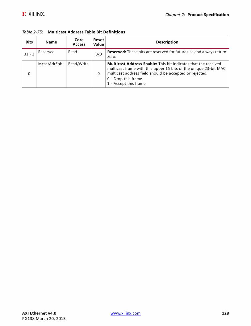
AXI Ethernet v4.0 www.xilinx.com 128PG138 March 20, 2013
Chapter 2: Product Specification
Table 2‐75: Multicast Address Table Bit Definitions
Bits NameCoreAccess
ResetValue Description
31 - 1 Reserved Read 0x0 Reserved: These bits are reserved for future use and always return zero.
0
McastAdrEnbl Read/Write
0
Multicast Address Enable: This bit indicates that the received multicast frame with this upper 15 bits of the unique 23-bit MAC multicast address field should be accepted or rejected.0 - Drop this frame1 - Accept this frame
AXI Ethernet v4.0 www.xilinx.com 129PG138 March 20, 2013
Chapter 3
Designing with the CoreThis chapter includes guidelines and additional information to facilitate designing with the core.
Design Guidelines
Understand the Features and Interfaces Provided by the Core Netlist
Chapter 1, Overview introduces the features and Chapter 2, Product Specification introduces the interfaces and registers space. This chapter provides design guidelines that need to be considered while creating the system using AXI Ethernet.
Customize and Generate the Core
Generate the core with your desired options using the IP catalog as described in Chapter 4, Customizing and Generating the Core.
Examine the generated design for this hierarchical block
• HDL is generated for this hierarchical block at locations as explained in Output Generation in Chapter 4.
• Examine this HDL for the I/O and interfaces generated. In many cases the required logic is generated automatically. Cross-check for the MDIO IOBUF instantiation as per the design requirement.
• Examine the Address Space that is allocated for AXI Ethernet in the IP Integrator Address editor tab. AXI Ethernet requires 256K Address Range.
• Examine the clocks required for the mode of operation and provide the clocks as required.

AXI Ethernet v4.0 www.xilinx.com 130PG138 March 20, 2013
Chapter 3: Designing with the Core
• If using a development board, check the board for the LOC constraints provided in the "Master Constraints" f ile delivered along with the board. Also check for the specif ic location constraints for transceivers.
• Synthesize and Implement the entire design.
• After implementation is complete you can also create a bitstream that can be downloaded to a Xilinx device.
Keep it Registered
To simplify timing and to increase system performance in an FPGA design, keep all inputs and outputs registered between the user application and the core. All inputs and outputs from the user application should come from, or connect to, a flip-flop. While registering signals might not be possible for all paths, it simplif ies timing analysis and makes it easier for the Xilinx tools to place and route the design.
Recognize Timing Critical Signals
The constraints provided with the Infrastructure cores identify the critical signals and the timing constraints that should be applied. See Chapter 5, Constraining the Core. Also refer to the infrastructure core documentation for more information.
Make Only Allowed Modifications
The AXI Ethernet IP core should not be modif ied. Modifications can have adverse effects on system timing and protocol compliance. Supported user configurations of this IP can only be made by selecting the options from within the Vivado™ design tools when the core is generated. See Vivado Integrated Design Environment in Chapter 4. Do not directly modify the infrastructure cores.
ClockingWhen targeting a GMII design, a BUFGMUX is used to switch between the MII_TX_CLK and the GTX_CLK clocks. This allows the design to support data rates of 10/100 Mb/s and 1000 Mb/s. The FPGA pins for these clocks must be selected such that they are located in the same clock region and they are both on clock dedicated pins. The GMII status, control, and data pins must be chosen to be in the same clock region as these clocks. See the Clocking Resources User Guide for the targeted FPGA family ([Ref 8]) for more information.
IMPORTANT: Pay special attention to clocking conflicts. Failure to adhere to these rules can cause build errors and data integrity errors.
AXI Ethernet v4.0 www.xilinx.com 131PG138 March 20, 2013
Chapter 3: Designing with the Core
ResetsThe TEMAC components are reset using the following AXI4 reset signals: AXI_STR_TXD_ARESETN, AXI_STR_TXC_ARESETN, AXI_STR_RXD_ARESETN, AXI_STR_RXS_ARESETN, or S_AXI_ARESETN. All resets must pass through reset detection circuits which detect and synchronize the resets to the different clock domains. As a result, any time AXI Ethernet core is reset, suff icient time must elapse for a reset to propagate through the reset circuits and logic. The amount of time required is dependent upon the slowest AXI Ethernet clock. Allow thirty clock cycles of the slowest AXI Ethernet clock, to elapse before accessing the core. Failure to do causes unpredictable behavior.
In a system in which Ethernet operates at 10 Mb/s, the MAC interface operates at 2.5 MHz. If the AXI4-Lite interface operates 100 MHz and the AXI4-Stream interface operates at 125 MHz, the time that must elapse before AXI Ethernet is accessed is 12 us (400 ns * 30 clock cycles).
If the system uses DMA for data transfer on the streaming interfaces, it is advised to connect the reset outputs from the DMA to the AXI Ethernet streaming reset inputs.
RECOMMENDED: As a general design guideline, Xilinx recommends asserting system ARESETN signals for a minimum of 30 clock cycles (of the slowest ACLK), as that is known to satisfy the preceding reset requirements.
Design ParametersTo allow you to generate an AXI Ethernet core that is uniquely tailored to your system, certain features can be parameterized in the AXI Ethernet design as shown in Table 3-1.
In addition to the parameters listed in Table 3-1, there are also parameters that are inferred for each AXI interface in the EDK tools. Through the design, these EDK-inferred parameters control the behavior of the AXI Interconnect. For a complete list of the interconnect settings related to the AXI interface, see the LogiCORE IP Tri-Mode Ethernet MAC Product Guide (PG051).

AXI Ethernet v4.0 www.xilinx.com 132PG138 March 20, 2013
Chapter 3: Designing with the Core
Table 3‐1: AXI Ethernet Core Design Parameters
Feature/Description Parameter Name Allowable ValuesDefaultValues
VHDLType
User Specified TEMAC Implementation Parameters
PHY Interface Type C_PHY_TYPE
0 = MII1 = GMII/MII2 = Reserved3 = RGMII v2.04 = SGMII5 = 1000Base-X
1 integer
PHY Address for Gigabit Ethernet PCS PMA C_PHYADDR(1) 00001 - 11111 00001 std_logic_
vector
Transmit block RAM depth in bytes for TEMAC C_TXMEM 2048, 4096, 8192, 16384, 32768 4096 integer
Receive block RAM depth in bytes for TEMAC C_RXMEM 2048, 4096, 8192, 16384, 32768 4096 integer
Transmit TCP/UDP Checksum off load C_TXCSUM
0 = Tx CSUM unused1 = Partial Tx CSUM used2 = Full Tx CSUM used
0 integer
Receive TCP/UDP Checksum off load C_RXCSUM
0 = Rx CSUM unused1 = Partial Rx CSUM used2 = Full Rx CSUM used
0 integer
Transmit VLAN tagging C_TXVLAN_TAG 1 = Tx VLAN tagging used0 = Tx VLAN tagging unused 0 integer
Receive VLAN tagging C_RXVLAN_TAG 1 = Rx VLAN tagging used0 = Rx VLAN tagging unused 0 integer
Transmit VLAN translation C_TXVLAN_TRAN 1 = Tx VLAN translation used0 = Tx VLAN translation unused 0 integer
Receive VLAN translation C_RXVLAN_TRAN 1 = Rx VLAN translation used0 = Rx VLAN translation unused 0 integer
Transmit VLAN stripping C_TXVLAN_STRP 1 = Tx VLAN stripping used0 = Tx VLAN stripping unused 0 integer
Receive VLAN stripping C_RXVLAN_STRP 1 = Rx VLAN stripping used0 = Rx VLAN stripping unused 0 integer
Extended Multicast address filtering for RX C_MCAST_EXTEND
1 = Extended multicast f iltering used0 = Extended multicast f iltering unused
0 integer
Statistics gathering C_STATS 1 = Statistics gathering used0 = Statistics gathering unused 0 integer
Statistics width C_STATS_WIDTH 64 = 64-bit wide statistic vectors 64 integer
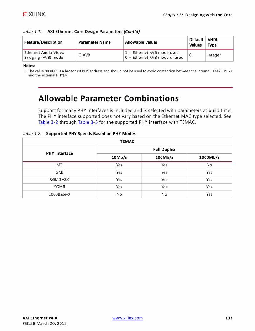
AXI Ethernet v4.0 www.xilinx.com 133PG138 March 20, 2013
Chapter 3: Designing with the Core
Allowable Parameter CombinationsSupport for many PHY interfaces is included and is selected with parameters at build time. The PHY interface supported does not vary based on the Ethernet MAC type selected. See Table 3-2 through Table 3-5 for the supported PHY interface with TEMAC.
Ethernet Audio Video Bridging (AVB) mode C_AVB 1 = Ethernet AVB mode used
0 = Ethernet AVB mode unused 0 integer
Notes: 1. The value “00000” is a broadcast PHY address and should not be used to avoid contention between the internal TEMAC PHYs
and the external PHY(s)
Table 3‐1: AXI Ethernet Core Design Parameters (Cont’d)
Feature/Description Parameter Name Allowable ValuesDefaultValues
VHDLType
Table 3‐2: Supported PHY Speeds Based on PHY Modes
TEMAC
PHY InterfaceFull Duplex
10Mb/s 100Mb/s 1000Mb/s
MII Yes Yes No
GMI Yes Yes Yes
RGMII v2.0 Yes Yes Yes
SGMII Yes Yes Yes
1000Base-X No No Yes
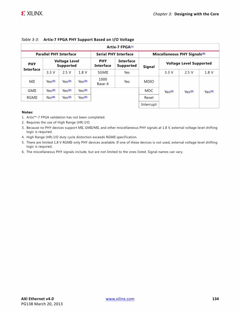
AXI Ethernet v4.0 www.xilinx.com 134PG138 March 20, 2013
Chapter 3: Designing with the Core
Table 3‐3: Artix‐7 FPGA PHY Support Based on I/O Voltage
Artix‐7 FPGA(1)
Parallel PHY Interface Serial PHY Interface Miscellaneous PHY Signals(6)
PHYInterface
Voltage Level Supported
PHY Interface
Interface Supported Signal
Voltage Level Supported
3.3 V 2.5 V 1.8 V SGMII Yes 3.3 V 2.5 V 1.8 V
MII Yes(2) Yes(2) Yes(3) 1000 Base-X Yes MDIO
Yes(2) Yes(2) Yes(3)GMII Yes(2) Yes(2) Yes(3) MDC
RGMII No(4) Yes(2) Yes(5) Reset
Interrupt
Notes: 1. Artix™-7 FPGA validation has not been completed.2. Requires the use of High Range (HR) I/O.3. Because no PHY devices support MII, GMII/MII, and other miscellaneous PHY signals at 1.8 V, external voltage level shifting
logic is required.4. High Range (HR) I/O duty cycle distortion exceeds RGMII specif ication.5. There are limited 1.8 V RGMII-only PHY devices available. If one of these devices is not used, external voltage level shifting
logic is required.6. The miscellaneous PHY signals include, but are not limited to the ones listed. Signal names can vary.

AXI Ethernet v4.0 www.xilinx.com 135PG138 March 20, 2013
Chapter 3: Designing with the Core
Table 3‐4: Virtex‐7 FPGA PHY Support Based on I/O Voltage
Virtex‐7 FPGA
Parallel PHY Interface Serial PHY Interface Miscellaneous PHY Signals(5)
PHYInterface
Voltage Level Supported
PHY Interface
Interface Supported Signal
Voltage Level Supported
3.3 V 2.5 V 1.8 V SGMII Yes 3.3 V 2.5 V 1.8 V
MII Yes(1) Yes(1) Yes(2) 1000 Base-X Yes MDIO
Yes(1) Yes(1) Yes(2)GMII Yes(1) Yes(1) Yes(2) MDC
RGMII No(3) No(3) Yes(4) Reset
Interrupt
Notes: 1. Supported on the XC7V585T-FFG1761, XC7VX330T-FFG1761 devices when using the High Range (HR). Other devices do not
contain HR I/O; therefore these voltages are not supported.2. Because no PHY devices support MII, GMII/MII, and other miscellaneous PHY signals at 1.8 V, external voltage level shifting
logic is required.3. High Range (HR) I/O duty cycle distortion exceeds RGMII specif ication.4. There are limited 1.8 V RGMII-only PHY devices available. If one of these devices is not used, external voltage level shifting
logic is required.5. The miscellaneous PHY signals include, but are not limited to the ones listed. Signal names can vary.
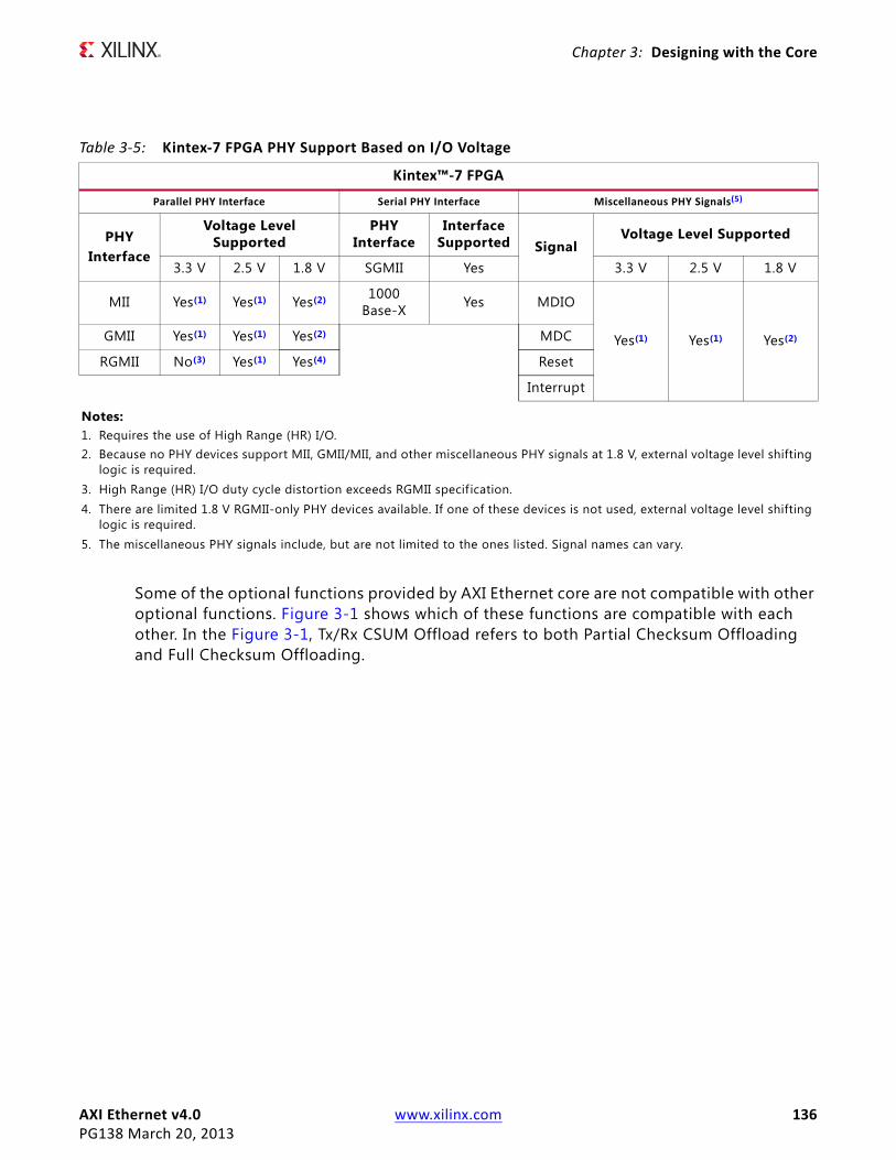
AXI Ethernet v4.0 www.xilinx.com 136PG138 March 20, 2013
Chapter 3: Designing with the Core
Some of the optional functions provided by AXI Ethernet core are not compatible with other optional functions. Figure 3-1 shows which of these functions are compatible with each other. In the Figure 3-1, Tx/Rx CSUM Offload refers to both Partial Checksum Offloading and Full Checksum Offloading.
Table 3‐5: Kintex‐7 FPGA PHY Support Based on I/O Voltage
Kintex™‐7 FPGA
Parallel PHY Interface Serial PHY Interface Miscellaneous PHY Signals(5)
PHYInterface
Voltage Level Supported
PHY Interface
Interface Supported Signal
Voltage Level Supported
3.3 V 2.5 V 1.8 V SGMII Yes 3.3 V 2.5 V 1.8 V
MII Yes(1) Yes(1) Yes(2) 1000 Base-X Yes MDIO
Yes(1) Yes(1) Yes(2)GMII Yes(1) Yes(1) Yes(2) MDC
RGMII No(3) Yes(1) Yes(4) Reset
Interrupt
Notes: 1. Requires the use of High Range (HR) I/O.2. Because no PHY devices support MII, GMII/MII, and other miscellaneous PHY signals at 1.8 V, external voltage level shifting
logic is required.3. High Range (HR) I/O duty cycle distortion exceeds RGMII specif ication.4. There are limited 1.8 V RGMII-only PHY devices available. If one of these devices is not used, external voltage level shifting
logic is required.5. The miscellaneous PHY signals include, but are not limited to the ones listed. Signal names can vary.

AXI Ethernet v4.0 www.xilinx.com 137PG138 March 20, 2013
Chapter 3: Designing with the Core
The AXI Ethernet core provides one Ethernet interface. Access to external PHY registers is provided using a standard MII Management bus. When using the SGMII or 1000 Base-X PHY interfaces, the AXI Ethernet core provides some PHY functionality and as a result also includes PHY registers which are also accessible through the MII Management bus. These registers are described in Using the MII Management to Access Internal or External PHY Registers.
This core includes optional logic to calculate TCP/UDP checksums for transmit and verify TCP/UDP checksums for receive. Using this logic can significantly increase the maximum Ethernet bus data rate while reducing utilization of the processor for Ethernet tasks. Including the checksum off-load function increases the amount of FPGA resources used for this core. The checksum information is included with each Ethernet frame passing over the AXI4-Stream interface. The checksum off load functionality cannot be used at the same time as the extended VLAN functionality.
X-Ref Target - Figure 3-1
Figure 3‐1: Option Function Compatibility

AXI Ethernet v4.0 www.xilinx.com 138PG138 March 20, 2013
Chapter 3: Designing with the Core
The AXI Ethernet core provides memory buffering of transmit and receive Ethernet frames, thereby allowing more optimal transfer to and from the core with DMA. The number of frames that can be buffered in each direction is based on the size of each frame and the size of the memory buffer which are selected by parameters at build time. If the AXI Ethernet core transmit memory buffer becomes full, it throttles the transmit AXI4-Stream Data interface until more room is available for Ethernet frames. If the receive memory buffer becomes full, frames are dropped until more memory buffer room is available. Receive frames that do not meet Ethernet format rules or do not satisfy receive address qualif ication are always dropped.
Optional logic can be included to facilitate handling of VLAN type frames. Auto insertion, stripping, or translation of VLAN frames can be performed on transmit or receive with several options for choosing which frames are to be altered. Additional logic can be selected to provide additional f iltering of receive frames with multicast destination addresses. The AXI Ethernet core provides native support for up to four (4) multicast addresses.
Logic can be selected to gather statistics on transmit and receive frames. This logic provides 64-bit counters for many statistics about the frames passing through the TEMAC core. Ethernet AVB support is available with an additional license and is supported at 100 Mb/s or 1000 Mb/s implementations.

AXI Ethernet v4.0 www.xilinx.com 139PG138 March 20, 2013
Chapter 4
Customizing and Generating the CoreThis chapter includes information about using Xilinx tools to customize and generate the core in the Vivado™ Design Suite.
Vivado Integrated Design EnvironmentX-Ref Target - Figure 4-1
Figure 4‐1: Top Tab

AXI Ethernet v4.0 www.xilinx.com 140PG138 March 20, 2013
Chapter 4: Customizing and Generating the Core
The AXI Ethernet core can be configured by selecting the options from the customization Vivado Integrated Design Environment (IDE). These options are related to the RTL parameters. If any option combination is not allowed, those options are grayed out for ease of use.
The first tab is shown in Figure 4-1. In this tab options available are
• Physical Interface Type: The physical interface type is selected using this option. The PHY types supported are MII, GMI, RGMII, SGMII, and 1000BaseX.
• AVB Option: AVB mode of operation can be selected using this option.
• Statistics Counter Options: Use this option to enable the statistic counters. “Enable Statistics Counters” should be selected for this purpose. By selecting the “Statistics Reset” option the statistics reset capability can be enabled. The width of the statistics counter can be selected using the “Statistics Width” option.
The second tab is shown in Figure 4-2. In this tab additional configuration options are shown.
• TX and RX memory sizes can be selected using the TX memory and RX memory size options,
• TX and RX checksum offload capability can be selected using the RX checksum offload option and TX checksum offload option.
• Advanced VLAN options for TX and RX data streams for VLAN tagging, VLAN stripping, and VLAN translation are selected using the respective buttons.
• RX extended multicast f iltering can be enabled using this “Enable RX extended multicast address f iltering” option.
• The Gigabit Ethernet PCS PMA phy address can be configured using this option.

AXI Ethernet v4.0 www.xilinx.com 141PG138 March 20, 2013
Chapter 4: Customizing and Generating the Core
Output GenerationThe AXI Ethernet core deliverables are organized in the directory <projectname>/<projectname>.srcs/sources_1/bd/<designname>/ip/<component name> and is designated as the <ip_source_dir>. The relevant contents of the directories are described in the following sections.
Vivado Design Tools Project Files
The Vivado design tools project f iles are located in the root of the <ip_source_dir>.
X-Ref Target - Figure 4-2
Figure 4‐2: Embedded Tab
Table 4‐1: Project File
Name Description
<component_name>.xciVivado design tools IP configuration options f ile. This f ile can be imported into any Vivado tools design and be used to generate all other IP source f iles.
<component_name>.xml Xml file related to the component
<projectname>/<projectname>.srcs/sources_1/bd/<designname>/hdl/<designname>.v*
Generated output hdl f iles. (verilog or VHDL based on project settings)

AXI Ethernet v4.0 www.xilinx.com 142PG138 March 20, 2013
Chapter 4: Customizing and Generating the Core
IP Sources
The IP sources are held in the subdirectories of <ip_source_dir>. The infrastructure cores that are used in a particular mode are only generated. Their output generations are given in detail in their PG documents
Table 4‐2: IP sources
Name Description
<ip_source_dir>/<infrastructure_core>/*.xciVivado design tools IP configuration options f ile. This f ile can be imported into any Vivado tools design and be used to generate all other IP source files.
<ip_source_dir>/<infrastructure_core>/synth/* Source files of the core for synthesis (optional, generated if synthesis target selected)
<ip_source_dir>/<infrastructure_core>/sim/* Source files of the core for simulation (optional, generated if simulation target selected)
AXI Ethernet v4.0 www.xilinx.com 143PG138 March 20, 2013
Chapter 5
Constraining the CoreThis chapter contains information about constraining the core in the Vivado™ Design Suite environment.
Required ConstraintsThe required constraints are taken from the dependent tri_mode_ethernet_mac and gig_ethernet_pcs_pma cores. This AXI Ethernet core does not have independent constraints.
Device, Package, and Speed Grade SelectionsThe selections need to be done in accordance with the requirements of the helper cores. See the LogiCORE™ IP Ethernet 1000BASE-X PCS/PMA or SGMII Product Guide (PG047) and LogiCORE IP Tri-Mode Ethernet MAC Product Guide (PG051) for more details.
Clock PlacementThe clock buffer needs to be placed in accordance with the requirements of the helper cores. See the LogiCORE IP Ethernet 1000BASE-X PCS/PMA or SGMII Product Guide (PG047) and LogiCORE IP Tri-Mode Ethernet MAC Product Guide (PG051) for more details.
BankingThere is no information currently provided for this core.

AXI Ethernet v4.0 www.xilinx.com 144PG138 March 20, 2013
Chapter 5: Constraining the Core
Transceiver PlacementThe transceiver placements should be done in accordance with the requirement of Gigabit Ethernet PCS PMA. See the LogiCORE IP Ethernet 1000BASE-X PCS/PMA or SGMII Product Guide (PG047).
I/O Standard and PlacementThe I/O standards and placements needs to be placed in accordance with the requirements of the helper cores. See the LogiCORE IP Ethernet 1000BASE-X PCS/PMA or SGMII Product Guide (PG047) and LogiCORE IP Tri-Mode Ethernet MAC Product Guide (PG051) for more details.

AXI Ethernet v4.0 www.xilinx.com 145PG138 March 20, 2013
Appendix A
MigratingThis appendix describes migrating from older versions of the IP to the current IP release.
For information on migrating to the Vivado™ Design Suite, see Vivado Design Suite Migration Methodology Guide (UG911).
AXI Ethernet v4.0 www.xilinx.com 146PG138 March 20, 2013
Appendix B
DebuggingThis appendix includes details about resources available on the Xilinx Support website and debugging tools. In addition, this appendix provides a step-by-step debugging process and a flow diagram to guide you through debugging the AXI Ethernet core.
The following topics are included in this appendix:
• Finding Help on Xilinx.com
• Debug Tools
• Interface Debug
• Hardware Debug
• Interface Debug
Finding Help on Xilinx.comTo help in the design and debug process when using the AXI Ethernet core, the Xilinx Support web page (www.xilinx.com/support) contains key resources such as product documentation, release notes, answer records, information about known issues, and links for opening a Technical Support WebCase.
Documentation
This product guide is the main document associated with the AXI Ethernet core. This guide, along with documentation related to all products that aid in the design process, can be found on the Xilinx Support web page (www.xilinx.com/support) or by using the Xilinx Documentation Navigator.
Download the Xilinx Documentation Navigator from the Design Tools tab on the Downloads page (www.xilinx.com/download). For more information about this tool and the features available, open the online help after installation.

AXI Ethernet v4.0 www.xilinx.com 147PG138 March 20, 2013
Appendix B: Debugging
Solution Centers
See the Xilinx Solution Centers for support on devices, software tools, and intellectual property at all stages of the design cycle. Topics include design assistance, advisories, and troubleshooting tips.
The Solution Center specif ic to the AXI Ethernet core is Xilinx Ethernet IP Solution Center.
Answer Records
Answer Records include information about commonly encountered problems, helpful information on how to resolve these problems, and any known issues with a Xilinx product. Answer Records are created and maintained daily ensuring that users have access to the most accurate information available.
Answer Records for this core can also be located by using the Search Support box on the main Xilinx support web page. To maximize your search results, use proper keywords such as
• Product name
• Tool message(s)
• Summary of the issue encountered
A filter search is available after results are returned to further target the results.
Master Answer Record for the AXI Ethernet core
AR 54688
Contacting Technical Support
Xilinx provides technical support at www.xilinx.com/support for this LogiCORE™ IP product when used as described in the product documentation. Xilinx cannot guarantee timing, functionality, or support of product if implemented in devices that are not defined in the documentation, if customized beyond that allowed in the product documentation, or if changes are made to any section of the design labeled DO NOT MODIFY.
AXI Ethernet v4.0 www.xilinx.com 148PG138 March 20, 2013
Appendix B: Debugging
To contact Xilinx Technical Support:
1. Navigate to www.xilinx.com/support.
2. Open a WebCase by selecting the selecting the WebCase link located under Additional Resources.
When opening a WebCase, include:
• Target FPGA including package and speed grade.
• All applicable Xilinx Design Tools and simulator software versions.
• Additional f iles based on the specif ic issue might also be required. See the relevant sections in this debug guide for guidelines about which f ile(s) to include with the WebCase.
Debug ToolsThere are many tools available to address AXI Ethernet core design issues. It is important to know which tools are useful for debugging various situations.
Vivado Lab Tools
Vivado™ lab tools insert logic analyzer and virtual I/O cores directly into your design. Vivado lab tools allows you to set trigger conditions to capture application and integrated block port signals in hardware. Captured signals can then be analyzed. This feature represents the functionality in the Vivado IDE that is used for logic debugging and validation of a design running in Xilinx devices in hardware.
The Vivado logic analyzer is used to interact with the logic debug LogiCORE™ IP cores, including:
• ILA 2.0 (and later versions)
• VIO 2.0 (and later versions)
Reference Boards
Various Xilinx development boards support AXI Ethernet core. The KC705 7 series FPGA evaluation board can be used to prototype designs and establish that the core can communicate with the system.
AXI Ethernet v4.0 www.xilinx.com 149PG138 March 20, 2013
Appendix B: Debugging
Hardware DebugHardware issues can range from link bring-up to problems seen after hours of testing. This section provides debug steps for common issues. The Vivado lab tools are a valuable resource to use in hardware debug. The signal names mentioned in the following individual sections can be probed using the Vivado lab tools for debugging the specific problems.
Ensure that all the timing constraints for the core were properly incorporated from the example design and that all constraints were met during implementation. Following is a list of some general checks.
• Does it work in post-place and route timing simulation? If problems are seen in hardware but not in timing simulation, this could indicate a PCB issue. Ensure that all clock sources are active and clean.
• If using MMCMs in the design, ensure that all MMCMs have obtained lock by monitoring the LOCKED port.
• If your outputs go to 0, check your licensing.
• Different PHYs have different reset polarity. Please check the reset polarity.
Interface Debug
AXI4‐Lite Interfaces
Read from a register that does not have all 0s as a default to verify that the interface is functional. Output s_axi_arready asserts when the read address is valid, and output s_axi_rvalid asserts when the read data/response is valid.
If the interface is unresponsive, ensure that the following conditions are met:
• The S_AXI_ACLK and ACLK inputs are connected and toggling.
• The interface is not being held in reset, and S_AXI_ARESET is an active-Low reset.
• The interface is enabled, and s_axi_aclken is active-High (if used).
• The main core clocks are toggling and that the enables are also asserted.
• If the simulation has been run, verify in simulation and/or the Vivado lab tools capture that the waveform is correct for accessing the AXI4-Lite interface.
AXI Ethernet v4.0 www.xilinx.com 150PG138 March 20, 2013
Appendix B: Debugging
AXI4‐Stream Interfaces
If data is not being transmitted or received, check the following conditions:
• If transmit <interface_name>_tready is stuck low following the <interface_name>_tvalid input being asserted, the core cannot send data.
• If the receive <interface_name>_tvalid is stuck low, the core is not receiving data.
• Check that the ACLK inputs are connected and toggling.
• Check that the AXI4-Stream waveforms are being followed. See Figure 2-21, Figure 2-23, Figure 2-25, and Figure 2-26.
• Check core configuration.
• Add appropriate core specif ic checks.

AXI Ethernet v4.0 www.xilinx.com 151PG138 March 20, 2013
Appendix C
Additional Resources
Xilinx ResourcesFor support resources such as Answers, Documentation, Downloads, and Forums, see the Xilinx Support website at:
www.xilinx.com/support.
For a glossary of technical terms used in Xilinx documentation, see:
www.xilinx.com/company/terms.htm.
ReferencesUnless otherwise noted, IP references are for the product documentation page. Reference the change log for a list of the cores utilized in this design. The change log also identif ies the version of the cores used and referenced throughout this document.
1. 7 Series FPGAs Overview (DS180)
2. ARM® AMBA® AXI Protocol v2.0 Specification (ARM IHI 0022C)
3. ARM AMBA 4 AXI4-Stream Protocol v1.0 Specification (ARM IHI 0051A)
4. LogiCORE IP AXI Interconnect Product Guide (PG059)
5. Xilinx Constraints Guide (UG625)
6. LogiCORE IP Tri-Mode Ethernet MAC Product Guide (PG051)
7. LogiCORE IP Ethernet 1000BASE-X PCS/PMA or SGMII Product Guide (PG047)
8. 7 Series documentation
9. Vivado™ design tools user documentation
10. Vivado Design Suite User Guide: Designing with IP (UG896)
11. Vivado Design Suite Migration Methodology Guide (UG911)
AXI Ethernet v4.0 www.xilinx.com 152PG138 March 20, 2013
Appendix C: Additional Resources
Revision HistoryThe following table shows the revision history for this document.
Notice of DisclaimerThe information disclosed to you hereunder (the “Materials”) is provided solely for the selection and use of Xilinx products. To the maximum extent permitted by applicable law: (1) Materials are made available “AS IS” and with all faults, Xilinx hereby DISCLAIMS ALL WARRANTIES AND CONDITIONS, EXPRESS, IMPLIED, OR STATUTORY, INCLUDING BUT NOT LIMITED TO WARRANTIES OF MERCHANTABILITY, NON-INFRINGEMENT, OR FITNESS FOR ANY PARTICULAR PURPOSE; and (2) Xilinx shall not be liable (whether in contract or tort, including negligence, or under any other theory of liability) for any loss or damage of any kind or nature related to, arising under, or in connection with, the Materials (including your use of the Materials), including for any direct, indirect, special, incidental, or consequential loss or damage (including loss of data, profits, goodwill, or any type of loss or damage suffered as a result of any action brought by a third party) even if such damage or loss was reasonably foreseeable or Xilinx had been advised of the possibility of the same. Xilinx assumes no obligation to correct any errors contained in the Materials or to notify you of updates to the Materials or to product specifications. You may not reproduce, modify, distribute, or publicly display the Materials without prior written consent. Certain products are subject to the terms and conditions of the Limited Warranties which can be viewed at http://www.xilinx.com/warranty.htm; IP cores may be subject to warranty and support terms contained in a license issued to you by Xilinx. Xilinx products are not designed or intended to be fail-safe or for use in any application requiring fail-safe performance; you assume sole risk and liability for use of Xilinx products in Critical Applications: http://www.xilinx.com/warranty.htm#critapps.© Copyright 2013 Xilinx, Inc. Xilinx, the Xilinx logo, Artix, ISE, Kintex, Spartan, Virtex, Vivado, Zynq, and other designated brands included herein are trademarks of Xilinx in the United States and other countries. AMBA, AMBA Designer, ARM, ARM1176JZ-S, CoreSight, Cortex, and PrimeCell are trademarks of ARM in the EU and other countries. All other trademarks are the property of their respective owners.
Date Version Revision
03/20/2013 1.0 Initial Xilinx release of this product guide. It replaces ds759.
Related Documents


