arXiv:0907.3904v2 [cond-mat.supr-con] 13 Nov 2009 Localization of Metal-Induced Gap States at the Metal-Insulator Interface: Origin of Flux Noise in SQUIDs and Superconducting Qubits SangKook Choi, 1, 2 Dung-Hai Lee, 1, 2 Steven G. Louie, 1, 2 and John Clarke 1, 2, ∗ 1 Department of Physics, University of California, Berkeley, California 94720 2 Materials Sciences Division, Lawrence Berkeley National Laboratory, Berkeley, California 94720 (Dated: November 13, 2009) Abstract The origin of magnetic flux noise in Superconducting Quantum Interference Devices with a power spectrum scaling as 1/f (f is frequency) has been a puzzle for over 20 years. This noise limits the decoherence time of superconducting qubits. A consensus has emerged that the noise arises from fluctuating spins of localized electrons with an areal density of 5 × 10 17 m −2 . We show that, in the presence of potential disorder at the metal-insulator interface, some of the metal-induced gap states become localized and produce local moments. A modest level of disorder yields the observed areal density. PACS numbers: 03.67.Lx, 05.40.Ca, 73.20.Fz, 75.20.-g, 85.25.Dq 1

Welcome message from author
This document is posted to help you gain knowledge. Please leave a comment to let me know what you think about it! Share it to your friends and learn new things together.
Transcript
arX
iv:0
907.
3904
v2 [
cond
-mat
.sup
r-co
n] 1
3 N
ov 2
009
Localization of Metal-Induced Gap States at the Metal-Insulator
Interface:
Origin of Flux Noise in SQUIDs and Superconducting Qubits
SangKook Choi,1, 2 Dung-Hai Lee,1, 2 Steven G. Louie,1, 2 and John Clarke1, 2, ∗
1Department of Physics, University of California, Berkeley, California 94720
2Materials Sciences Division, Lawrence Berkeley
National Laboratory, Berkeley, California 94720
(Dated: November 13, 2009)
Abstract
The origin of magnetic flux noise in Superconducting Quantum Interference Devices with a power
spectrum scaling as 1/f (f is frequency) has been a puzzle for over 20 years. This noise limits the
decoherence time of superconducting qubits. A consensus has emerged that the noise arises from
fluctuating spins of localized electrons with an areal density of 5 × 10¹⁷m−2. We show that, in
the presence of potential disorder at the metal-insulator interface, some of the metal-induced gap
states become localized and produce local moments. A modest level of disorder yields the observed
areal density.
PACS numbers: 03.67.Lx, 05.40.Ca, 73.20.Fz, 75.20.-g, 85.25.Dq
1

Well below 1 K, low-transition temperature Superconducting Quantum Interference De-
vices [1] (SQUIDs) exhibit magnetic flux noise [2] with a temperature-independent spectral
density scaling as 1/fα, where f is frequency and 0.6 ≤ α ≤ 1. The noise magnitude, a
few µΦ0Hz−1/2 at 1 Hz (Φ0 is the flux quantum), scales slowly with the SQUID area, and
does not depend significantly on the nature of the thin film superconductor or the substrate
on which it is deposited. The substrate is typically silicon or sapphire, which are insulators
at low temperature (T ) [2]. Flux noise of similar magnitude is observed in flux [3, 4] and
phase [5] qubits. Flux noise limits the decoherence time of superconducting, flux sensitive
qubits making scale-up for quantum computing problematic. The near-insensitivity of noise
magnitude to device area [2, 5, 6] suggests the origin of the noise is local. Koch et al. [7]
proposed a model in which electrons hop stochastically between traps with different prefer-
ential spin orientations. A broad distribution of time constants is necessary to produce a 1/f
power spectrum [8, 9]. They found that the major noise contribution arises from electrons
above and below the superconducting loop of the SQUID or qubit [5, 7], and that an areal
density of about 5 × 10¹⁷m−2 unpaired spins is required to account for the observed noise
magnitude. De Sousa [10] proposed that the noise arises from spin flips of paramagnetic
dangling bonds at the Si-SiO2 interface. Assuming an array of localized electrons, Faoro
and Ioffe [11] suggested that the noise results from electron spin diffusion. Sendelbach et
al. [12] showed that thin-film SQUIDs are paramagnetic, with a Curie (1/T ) susceptibility.
Assuming the paramagnetic moments arise from localized electrons, they deduced an areal
density of 5×10¹⁷m−2. Subsequently, Bluhm et al. [13] used a scanning SQUID microscope
to measure the low-T paramagnetic response of (nonsuperconducting) Au rings deposited
on Si substrates, and reported an areal density of 4× 10¹⁷m−2 for localized electrons. Para-
magnetism was not observed on the bare Si substrate.
In this Letter we propose that the local magnetic moments originate in metal-induced
gap states (MIGS) [14] localized by potential disorder at the metal-insulator interface. At
an ideal interface, MIGS are states in the band gap that are evanescent in the insulator and
extended in the metal [14] (Fig.1). In reality, at a nonepitaxial metal-insulator interface
there are inevitably random fluctuations in the electronic potential. The MIGS are particu-
larly sensitive to these potential fluctuations, and a significant fraction of them–with single
occupancy–becomes strongly localized near the interface, producing the observed paramag-
netic spins. Fluctuations [15] of these local moments yield T -independent 1/f flux noise.
2
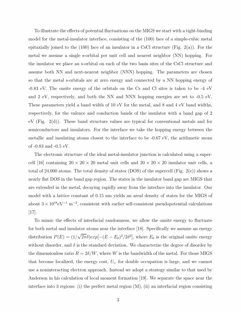
To illustrate the effects of potential fluctuations on the MIGS we start with a tight-binding
model for the metal-insulator interface, consisting of the (100) face of a simple-cubic metal
epitaxially joined to the (100) face of an insulator in a CsCl structure (Fig. 2(a)). For the
metal we assume a single s-orbital per unit cell and nearest neighbor (NN) hopping. For
the insulator we place an s-orbital on each of the two basis sites of the CsCl structure and
assume both NN and next-nearest neighbor (NNN) hopping. The parameters are chosen
so that the metal s-orbitals are at zero energy and connected by a NN hopping energy of
-0.83 eV. The onsite energy of the orbitals on the Cs and Cl sites is taken to be -4 eV
and 2 eV, respectively, and both the NN and NNN hopping energies are set to -0.5 eV.
These parameters yield a band width of 10 eV for the metal, and 8 and 4 eV band widths,
respectively, for the valence and conduction bands of the insulator with a band gap of 2
eV (Fig. 2(d)). These band structure values are typical for conventional metals and for
semiconductors and insulators. For the interface we take the hopping energy between the
metallic and insulating atoms closest to the interface to be -0.67 eV, the arithmetic mean
of -0.83 and -0.5 eV.
The electronic structure of the ideal metal-insulator junction is calculated using a super-
cell [16] containing 20 × 20 × 20 metal unit cells and 20 × 20 × 20 insulator unit cells, a
total of 24,000 atoms. The total density of states (DOS) of the supercell (Fig. 2(e)) shows a
nearly flat DOS in the band gap region. The states in the insulator band gap are MIGS that
are extended in the metal, decaying rapidly away from the interface into the insulator. Our
model with a lattice constant of 0.15 nm yields an areal density of states for the MIGS of
about 3× 10¹⁸eV−1 m−2, consistent with earlier self-consistent pseudopotential calculations
[17].
To mimic the effects of interfacial randomness, we allow the onsite energy to fluctuate
for both metal and insulator atoms near the interface [18]. Specifically we assume an energy
distribution P (E) = (1/√
2πδ)exp[−(E − E0)2/2δ2], where E0 is the original onsite energy
without disorder, and δ is the standard deviation. We characterize the degree of disorder by
the dimensionless ratio R = 2δ/W , where W is the bandwidth of the metal. For those MIGS
that become localized, the energy cost, Ui, for double occupation is large, and we cannot
use a noninteracting electron approach. Instead we adopt a strategy similar to that used by
Anderson in his calculation of local moment formation [19]. We separate the space near the
interface into 3 regions: (i) the perfect metal region (M), (ii) an interfacial region consisting
3

of 2 layers of metal unit cells and 2 layers of insulator unit cells (D) (Fig. 2(b)), and (iii) the
perfect insulator region (I). Region (ii) is analogous to the impurity in Anderson’s analysis.
We first compute the single-particle eigenstates, ϕi(r), of region D in isolation. For each
of these states, we compute Ui (using a long-range Coulomb potential with an onsite cutoff
of 10 eV) and the hybridization energy Γi due to hopping to the metal and the insulator [20].
With the computed values of Ui and Γi , we solve Anderson’s equation for the spin-dependent
occupation for each localized state | i〉:
〈ni,σ〉 =1
π
∫ EF
−∞
dE ′ Γi
(E ′ − Ei,σ)2 + Γi2 . (1)
Here, Ei,σ = Ei + Ui〈ni,−σ〉 and σ is the spin index. The net moment associated with the
state is given by mi = µB|〈ni,σ〉 − 〈ni,−σ〉|. Equation (1) and the associated expression for
the net moment of the localized states are calculated within the self-consistent Hartree-Fock
approximation [19]. An mi 6= 0 solution is obtained only when Ui/(EF − Ei) exceeds a
critical value which depends on Γi/(EF − Ei). In the large Ui limit, it is more appropriate
to start from the weak coupling limit (Γi = 0), where the localized state is populated by
a single electron, and treat Γi as a perturbation. By calculating the areal density of such
moment-bearing localized states we estimate the density of spin-12
local moments.
Figure 3 shows the calculated distribution ρ(E, U) in the isolated interfacial region for
R= 0.05, 0.1, 0.15, 0.2, 0.25, and 0.3; for each value, higher values of U correspond to
more localized states. As expected we see that, for any given degree of randomness, the
states with energy inside the insulator band gap (the MIGS) or those at the band edges are
most susceptible to localization. Figure 4 shows a perspective plot of the charge density of
two states, with high and low values of Ui, showing the correlation between the degree of
wavefunction localization and the value of Ui. Both states are centered in the insulator, a
general characteristic of localized states in the band gap originating from the MIGS.
Setting the Fermi energy at the insulator midgap value, we estimate the areal density of
spins for a given degree of randomness R. The top panel in Fig. 5 depicts the distribution
ρ(E, m) of the spin moments as a function of energy. We see that for small R virtually all the
local moments are derived from the MIGS. The bottom panel of Fig. 5 shows the calculated
areal density of local moments versus R. Our simple model thus indicates that moderate
potential fluctuations (R ∼ 0.15) at the interface produce an areal density of localized
moments comparable to experimental values [21]. Although our analysis is for a specific
4

model, we expect the general physical picture to remain valid for real materials. First, the
formation of MIGS at a metal-insulator interface is universal, and their areal density is
rather insensitive to the nature of the materials as discussed in supplements [20] and shown
numerically in Ref. [17]. Second, the formation of local moments from the combination of
localized states and Coulomb interaction is a general phenomenon [19]. We also note that
our analysis should not be significantly modified when the metal is superconducting. This
is because the Ui for the localized states is generally much greater than the pairing gap. Of
course, extended states with negligible Ui would be paired.
Given our picture of the origin of the localized spin-12
moments, how do they produce
1/f flux noise with a spectral density SΦ(f) ∝ 1/fα? The local moments interact via
mechanisms such as direct superexchange and the RKKY interaction [11, 22, 23, 24] between
themselves, and Kondo exchange with the quasiparticles in the superconductor. This system
can exhibit a spin-glass transition [25], which could account for the observed susceptibility
cusp [12] near 55 mK. For T > 55 mK, however, experiments suggest that the spins are
in thermal equilibrium [26] and exhibit a 1/T (Curie Law) static susceptibility [12, 13].
In this temperature regime, for hf << kBT standard linear response theory [27] shows
that the imaginary part of the dynamical susceptibility χ′′(f, T ) = A(f, T )(hf/kBT ). Here,
A(f, T ) ∝∑
µ
∑α,β Pαδ(hf + Eα − Eβ)|〈β | Sµ | α〉|2, where Sµ is the µ-th component of
the spin operator, α and β label the exact eigenstates, and Pα is the Boltzmann distribution
associated with state α. Combining the above result with the fluctuation-dissipation theorem
[15] which relates the flux noise to χ′′(f, T ), namely SΦ(f, T ) ∝ (kBT/hf)χ′′(f, T ), we
conclude that the observed 1/fα spectral density implies A(f, T ) ∝ 1/fα(0.6 ≤ α ≤ 1).
Assuming low frequency contributions dominate the Kramers-Kronig transform, this result
is consistent with the observed 1/T static susceptibility, and the recent measurement [28]
showing that flux noise in a SQUID is highly correlated with fluctuations in its inductance,
However, without knowing the form of the interaction between the spins, one cannot derive
this behavior for A(f, T ) theoretically.
In conclusion, we have presented a theory for the origin of the localized magnetic moments
which have been shown experimentally to give rise to the ubiquitous low-T flux 1/f noise
observed in SQUIDs and superconducting qubits. In particular we have shown that for
a generic metal-insulator interface, disorder localizes a substantial fraction of the metal-
induced gap states (MIGS), causing them to bear local moments. Although MIGS have
5
been known to exist at metal-insulator interfaces for three decades, we believe this is the
first understanding of their nature in the presence of strong local correlation and disorder.
Provided T is above any possible spin glass transition, experiments show that fluctuations
of these local moments produce a paramagnetic χ′ and a power-law, f -dependent χ′′ which
in turn leads to flux 1/f noise. It is important to realize that localized MIGS occur not
only at the metal-substrate interface but also at the interface between the metal and the
oxide that inevitably forms on the surface of superconducting films such as aluminum and
niobium. There are a number of open problems, for example, the precise interaction between
the local moments, its relation to the value of α, and the possibility of a spin glass phase
at low temperature. A particularly intriguing experimental issue to address is why different
metals and substrates evidently have such similar values of R, around 0.15. Experimentally,
to improve the performance of SQUIDs and superconducting qubits we need to understand
how to control and reduce the disorder at metal-insulator interfaces, for example, by growing
the superconductor epitaxially on its substrate.
We thank R.McDermott and K.A.Moler for prepublication copies of their papers. S.C.
and S.G.L. thank M.Jain and J.D.Sau for fruitful discussions. This work was supported
by the Director, Office of Science, Office of Basic Energy Sciences, Materials Science and
Engineering Division, of the U.S. Department of Energy under Contract No. DE-AC02-
05CH11231. S.C. acknowledges support from a Samsung Foundation.
6
Supplements
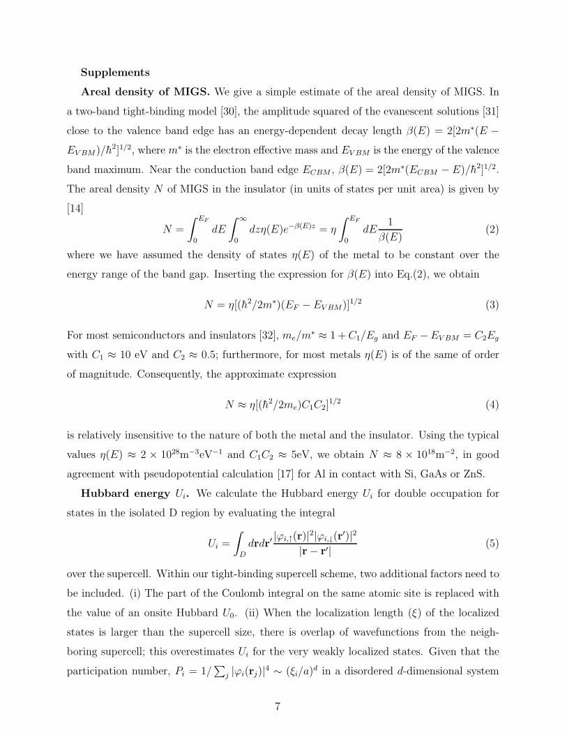
Areal density of MIGS. We give a simple estimate of the areal density of MIGS. In
a two-band tight-binding model [30], the amplitude squared of the evanescent solutions [31]
close to the valence band edge has an energy-dependent decay length β(E) = 2[2m∗(E −EV BM)/h2]1/2, where m∗ is the electron effective mass and EV BM is the energy of the valence
band maximum. Near the conduction band edge ECBM , β(E) = 2[2m∗(ECBM − E)/h2]1/2.
The areal density N of MIGS in the insulator (in units of states per unit area) is given by
[14]
N =
∫ EF
0
dE
∫ ∞
0
dzη(E)e−β(E)z = η
∫ EF
0
dE1
β(E)(2)
where we have assumed the density of states η(E) of the metal to be constant over the
energy range of the band gap. Inserting the expression for β(E) into Eq.(2), we obtain
N = η[(h2/2m∗)(EF − EV BM)]1/2 (3)
For most semiconductors and insulators [32], me/m∗ ≈ 1 + C1/Eg and EF −EV BM = C2Eg
with C1 ≈ 10 eV and C2 ≈ 0.5; furthermore, for most metals η(E) is of the same of order
of magnitude. Consequently, the approximate expression
N ≈ η[(h2/2me)C1C2]1/2 (4)
is relatively insensitive to the nature of both the metal and the insulator. Using the typical
values η(E) ≈ 2 × 1028m−3eV−1 and C1C2 ≈ 5eV, we obtain N ≈ 8 × 10¹⁸m−2, in good
agreement with pseudopotential calculation [17] for Al in contact with Si, GaAs or ZnS.
Hubbard energy Ui. We calculate the Hubbard energy Ui for double occupation for
states in the isolated D region by evaluating the integral
Ui =
∫D
drdr′|ϕi,↑(r)|2|ϕi,↓(r
′)|2|r− r′| (5)
over the supercell. Within our tight-binding supercell scheme, two additional factors need to
be included. (i) The part of the Coulomb integral on the same atomic site is replaced with
the value of an onsite Hubbard U0. (ii) When the localization length (ξ) of the localized
states is larger than the supercell size, there is overlap of wavefunctions from the neigh-
boring supercell; this overestimates Ui for the very weakly localized states. Given that the
participation number, Pi = 1/∑
j |ϕi(rj)|4 ∼ (ξi/a)d in a disordered d-dimensional system
7
with supercell lattice constant a and Ui ∝ 1/ξi, we map the Ui value of the finite supercell
onto that of an infinite supercell using a scaling law [33] for ξ.
Hybridization energy broadening Γi . The hybridization-energy broadening of the
localized states arises from couplings to the extended states in the metal as well as those in
the insulator, and is given by
Γi = ΓM
i+ Γ I
i(6)
ΓM
i= π|V M
i |2aveρM(E),Γ I
i= π|V I
i |2aveρI(E) (7)
where ρM(I)(E) is the density of extended states in M (I) at the energy of the localized
state E, and VM(I)i is the hopping matrix element between an extended state in M(I) and a
localized state in D (ave indicates averaging over the extended states). Extended eigenstates
in M(I) are a linear combination of constituent orbitals; the VM(I)i can then be expressed
in terms of the coupling of these orbitals to those in D. For example, the localized states
inside the band gap of the insulator are hybridized with only extended states in M, and
Γi = ΓM
i≈ πV 2di/W . (Here di is the charge of the localized state | i〉 in the unit cell layer
immediately adjacent to M.)
8

∗ Electronic address: [email protected]
[1] J.Clarke and A.I.Braginski, The SQUID Handbook (Wiley-VCH, GmbH and Weinheim, 2004),
Vol. 1.
[2] F.C.Wellstood, C.Urbina, and J.Clarke, Appl. Phys. Lett. 50, 772 (1987).
[3] F.Yoshihara, K.Harrabi, A.O.Niskanen, Y.Nakamura, and J.S.Tsai, Phys. Rev. Lett. 97,
167001 (2006).
[4] K.Kakuyanagi et al., Phys. Rev. Lett. 98, 047004 (2007).
[5] R.C.Bialczak et al., Phys. Rev. Lett. 99, 187006 (2007).
[6] T.Lanting et al., Phys. Rev. B 79, 060509(R) (2009).
[7] R.H.Koch, D.P.DiVincenzo, and J.Clarke, Phys. Rev. Lett. 98, 267003 (2007).
[8] S.J.Machlup, J. Appl. Phys. 25, 341 (1954).
[9] P.Dutta and P.M.Horn, Rev. Mod. Phys. 53, 497 (1981).
[10] R.de Sousa, Phys. Rev. B 76, 245306 (2007).
[11] L.Faoro and L.B.Ioffe, Phys. Rev. Lett. 100, 227005 (2008).
[12] S.Sendelbach et al., Phys. Rev. Lett. 100, 227006 (2008).
[13] H.Bluhm, J.A.Bert, N.C.Koshnick, M.E.Huber, and K.A.Moler, Phys. Rev. Lett. 103, 026805
(2009).
[14] S.G.Louie and M.L.Cohen, Phys. Rev. B 13, 2461 (1976).
[15] H.Nyquist, Phys. Rev. 32, 110 (1928).
[16] M.L.Cohen, M.Schlter, J.R.Chelikowsky, and S.G.Louie, Phys. Rev. B 12,5575 (1975).
[17] S.G.Louie, J.R.Chelikowsky, and M.L.Cohen, Phys. Rev. B 15, 2154 (1977).
[18] P.W.Anderson, Phys. Rev. 109, 1492 (1958).
[19] P.W.Anderson, Phys. Rev. 124, 41 (1961).
[20] See supplements
[21] If one includes the effect of metallic screening from region M on Ui (Ref. [29]), Ui would
decrease by a factor of roughly 2 since the localized state in region I is located on average ∼ 3
unit cell layers from region M. We estimate this effect reduces the spin density by ∼ 50% at
each R value. As a result, R should be incresed by at most 10% to produce an areal density
of ∼ 5 × 10¹⁷m−2.
9
[22] M.A.Ruderman and C.Kittel, Phys. Rev. 96, 99 (1954).
[23] T.Kasuya, Prog. Theor. Phys. 16, 45 (1956).
[24] K.Yosida, Phys. Rev. 106, 893 (1957).
[25] M.B.Weissman, Rev. Mod. Phys. 65, 829 (1993).
[26] R.Harris et al., Phys. Rev. Lett. 101, 117003 (2008).
[27] A.L.Fetter and J.D.Walecka, Quantum Theory of Many-Particle Systems, (McGraw-Hill, New
York, 1971) p.298.
[28] S.Sendelbach, D.Hover, M.Muck, and R.McDermott, Phys. Rev. Lett. 103, 117001 (2009).
[29] J.D.Sau, J.B.Neaton, H.J.Choi, S.G.Louie, and M.L.Cohen, Phys. Rev. Lett. 101, 026804
(2008).
[30] J.K.Tomfohr and O.F.Sankey, Phys. Rev. B 65, 245105 (2002).
[31] W.Kohn, Phys. Rev. 115, 809 (1959).
[32] P.Y.Yu and M.Cardona, Fundamentals of Semiconductors: Physics and Materials Properties
(Springer, Berlin, 2005).
[33] A.MacKinnon and B.Kramer, Phys. Rev. Lett. 47, 1546 (1981).
10
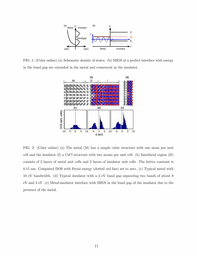
FIG. 1: (Color online) (a) Schematic density of states. (b) MIGS at a perfect interface with energy
in the band gap are extended in the metal and evanescent in the insulator.
FIG. 2: (Color online) (a) The metal (M) has a simple cubic structure with one atom per unit
cell and the insulator (I) a CsCl structure with two atoms per unit cell. (b) Interfacial region (D)
consists of 2 layers of metal unit cells and 2 layers of insulator unit cells. The lattice constant is
0.15 nm. Computed DOS with Fermi energy (dotted red line) set to zero. (c) Typical metal with
10 eV bandwidth. (d) Typical insulator with a 2 eV band gap separating two bands of about 8
eV and 4 eV. (e) Metal-insulator interface with MIGS in the band gap of the insulator due to the
presence of the metal.
11
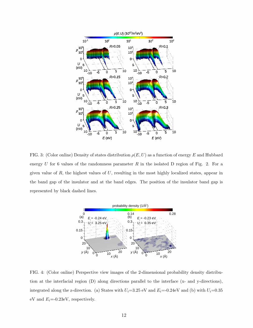
FIG. 3: (Color online) Density of states distribution ρ(E,U) as a function of energy E and Hubbard
energy U for 6 values of the randomness parameter R in the isolated D region of Fig. 2. For a
given value of R, the highest values of U , resulting in the most highly localized states, appear in
the band gap of the insulator and at the band edges. The position of the insulator band gap is
represented by black dashed lines.
FIG. 4: (Color online) Perspective view images of the 2-dimensional probability density distribu-
tion at the interfacial region (D) along directions parallel to the interface (x- and y-directions),
integrated along the z-direction. (a) States with Ui=3.25 eV and Ei=-0.24eV and (b) with Ui=0.35
eV and Ei=-0.23eV, respectively.
12

FIG. 5: (Color online) (a) Electron density distribution ρ(E,m) for 6 values of R. We simulated
5000 different configurations of disorder for each value of R. The position of the insulator band
gap is represented by black dashed lines. Virtually all the magnetic moments are from the MIGS
in the band gap of the insulator. (b) Integrated spin density versus randomness parameter R. For
R = 0.05, we estimate the spin density to be less than 0.01 × 10¹⁷m−2.
13
Related Documents