50 55 60 65 70 75 80 85 90 95 100 0 4 8 12 16 20 Efficiency (%) Output Current (A) PVIN = 3.3 V, VIN = 5 V PVIN = VIN = 5 V PVIN = VIN = 12 V C001 Vout = 1.8 V Fsw = 500 kHz VOUT AGND SENSE+ LMZ31520 FREQ_SEL SS_SEL V5V C O C I VIN VIN VOUT PGND VADJ R SET ILIM INH PWRGD PVIN Product Folder Order Now Technical Documents Tools & Software Support & Community Reference Design An IMPORTANT NOTICE at the end of this data sheet addresses availability, warranty, changes, use in safety-critical applications, intellectual property matters and other important disclaimers. PRODUCTION DATA. LMZ31520 SLVSBM9D – OCTOBER 2013 – REVISED APRIL 2018 LMZ31520 20-A Power Module With 3-V to 14.5-V Input in QFN Package 1 1 Features 1• Complete Integrated Power Solution; Smaller than a Discrete Design • 15 mm × 16 mm × 5.8 mm Package Size - Pin Compatible with LMZ31530 • Ultra-Fast Load Step Response • Efficiencies Up To 96% • Wide-Output Voltage Adjust 0.6 V to 3.6 V, with 1% Reference Accuracy • Optional Split Power Rails Allows Input Voltage Down to 3 V • Selectable Switching Frequency (300 kHz to 850 kHz) • Selectable Slow-Start • Adjustable Overcurrent Limit • Power Good Output • Output Voltage Sequencing • Over Temperature Protection • Pre-bias Output Start-up • Operating Temperature Range: –40°C to 85°C • Enhanced Thermal Performance: 8.6°C/W • Meets EN55022 Class A Emissions - Integrated Shielded Inductor • Create a Custom Design Using the LMZ31520 With the WEBENCH ® Power Designer 2 Applications • Broadband and Communications Infrastructure • DSP and FPGA Point of Load Applications • High Density Power Systems Efficiency 3 Description The LMZ31520 power module is an easy-to-use integrated power solution that combines a 20-A DC- DC converter with power MOSFETs, a shielded inductor, and passives into a low profile, QFN package. This total power solution allows as few as three external components and eliminates the loop compensation and magnetics part selection process. The 15×16×5.8 mm QFN package is easy to solder onto a printed circuit board and allows a compact point-of-load design. Achieves greater than 95% efficiency, has ultra-fast load step response and excellent power dissipation capability with a thermal impedance of 8.6°C/W. The LMZ31520 offers the flexibility and the feature-set of a discrete point-of- load design and is ideal for powering a wide range of ICs and systems. Advanced packaging technology affords a robust and reliable power solution compatible with standard QFN mounting and testing techniques. Simplified Application

Welcome message from author
This document is posted to help you gain knowledge. Please leave a comment to let me know what you think about it! Share it to your friends and learn new things together.
Transcript

50
55
60
65
70
75
80
85
90
95
100
0 4 8 12 16 20
Effi
cien
cy (
%)
Output Current (A)
PVIN = 3.3 V, VIN = 5 V
PVIN = VIN = 5 V
PVIN = VIN = 12 V
C001
Vout = 1.8 V Fsw = 500 kHz
VOUT
AGND
SENSE+
LMZ31520
FREQ_SEL
SS_SEL
V5V
CO
CI
VINVIN
VOUT
PGND
VADJ
RSET
ILIM
INH
PWRGD
PVIN
Product
Folder
Order
Now
Technical
Documents
Tools &
Software
Support &Community
ReferenceDesign
An IMPORTANT NOTICE at the end of this data sheet addresses availability, warranty, changes, use in safety-critical applications,intellectual property matters and other important disclaimers. PRODUCTION DATA.
LMZ31520SLVSBM9D –OCTOBER 2013–REVISED APRIL 2018
LMZ31520 20-A Power Module With 3-V to 14.5-V Inputin QFN Package
1
1 Features1• Complete Integrated Power Solution;
Smaller than a Discrete Design• 15 mm × 16 mm × 5.8 mm Package Size
- Pin Compatible with LMZ31530• Ultra-Fast Load Step Response• Efficiencies Up To 96%• Wide-Output Voltage Adjust
0.6 V to 3.6 V, with 1% Reference Accuracy• Optional Split Power Rails Allows
Input Voltage Down to 3 V• Selectable Switching Frequency
(300 kHz to 850 kHz)• Selectable Slow-Start• Adjustable Overcurrent Limit• Power Good Output• Output Voltage Sequencing• Over Temperature Protection• Pre-bias Output Start-up• Operating Temperature Range: –40°C to 85°C• Enhanced Thermal Performance: 8.6°C/W• Meets EN55022 Class A Emissions
- Integrated Shielded Inductor• Create a Custom Design Using the LMZ31520
With the WEBENCH® Power Designer
2 Applications• Broadband and Communications Infrastructure• DSP and FPGA Point of Load Applications• High Density Power Systems
Efficiency
3 DescriptionThe LMZ31520 power module is an easy-to-useintegrated power solution that combines a 20-A DC-DC converter with power MOSFETs, a shieldedinductor, and passives into a low profile, QFNpackage. This total power solution allows as few asthree external components and eliminates the loopcompensation and magnetics part selection process.
The 15×16×5.8 mm QFN package is easy to solderonto a printed circuit board and allows a compactpoint-of-load design. Achieves greater than 95%efficiency, has ultra-fast load step response andexcellent power dissipation capability with a thermalimpedance of 8.6°C/W. The LMZ31520 offers theflexibility and the feature-set of a discrete point-of-load design and is ideal for powering a wide range ofICs and systems. Advanced packaging technologyaffords a robust and reliable power solutioncompatible with standard QFN mounting and testingtechniques.
Simplified Application

2
LMZ31520SLVSBM9D –OCTOBER 2013–REVISED APRIL 2018 www.ti.com
Product Folder Links: LMZ31520
Submit Documentation Feedback Copyright © 2013–2018, Texas Instruments Incorporated
(1) Stresses beyond those listed under absolute maximum ratings may cause permanent damage to the device. These are stress ratingsonly, and functional operation of the device at these or any other conditions beyond those indicated under recommended operatingconditions is not implied. Exposure to absolute-maximum-rated conditions for extended periods may affect device reliability.
(2) See the temperature derating curves in the Typical Characteristics section for thermal information.(3) For soldering specifications, refer to the Soldering Requirements for BQFN Packages application note.(4) Devices with a date code prior to week 14 2018 (1814) have a peak reflow case temperature of 240°C with a maximum of one reflow
4 Specifications
4.1 Absolute Maximum Ratings (1)
over operating temperature range (unless otherwise noted)VALUE UNIT
MIN MAX
Input VoltageVIN, PVIN –0.3 20 VINH, VADJ, PWRGD, PWRGD_PU, ILIM, FREQ_SEL,SS_SEL, V5V
–0.3 7 V
Output VoltagePH –1 25 VPH 10ns Transient –2 27VOUT –0.3 6 V
VDIFF (GND to exposed thermalpad)
±200 mV
Operating Junction Temperature –40 125 (2) °CStorage Temperature –55 150 °CPeak Reflow Case Temperature (3) 245 (4) °CMaximum Number of Reflows Allowed (3) 3 (4)
Mechanical Shock Mil-STD-883D, Method 2002.3, 1 msec, 1/2 sine, mounted 250 GMechanical Vibration Mil-STD-883D, Method 2007.2, 20-2000Hz 20
4.2 Recommended Operating Conditionsover operating free-air temperature range (unless otherwise noted)
MIN MAX UNITPVIN Input Switching Voltage 3 14.5 VVIN Input Bias Voltage 4.5 14.5 VVOUT Output Voltage 0.6 3.6 VfSW Switching Frequency 300 850 kHz

3
LMZ31520www.ti.com SLVSBM9D –OCTOBER 2013–REVISED APRIL 2018
Product Folder Links: LMZ31520
Submit Documentation FeedbackCopyright © 2013–2018, Texas Instruments Incorporated
(1) For more information about traditional and new thermal metrics, see theSemiconductor and IC Package Thermal Metrics applicationreport (SPRA953).
(2) The junction-to-ambient thermal resistance, θJA, applies to devices soldered directly to a 100 mm x 100 mm, 6-layer PCB with 1 oz.copper and natural convection cooling. Additional airflow reduces θJA.
(3) The junction-to-ambient thermal resistance, θJA, applies to devices soldered directly to a 100 mm x 100 mm, 6-layer PCB with 1 oz.copper and 100 LFM forced air cooling. Additional airflow reduces θJA.
(4) The junction-to-top characterization parameter, ψJT, estimates the junction temperature, TJ, of a device in a real system, using aprocedure described in JESD51-2A (sections 6 and 7). TJ = ψJT * Pdis + TT; where Pdis is the power dissipated in the device and TT isthe temperature of the top of the device.
(5) The junction-to-board characterization parameter, ψJB, estimates the junction temperature, TJ, of a device in a real system, using aprocedure described in JESD51-2A (sections 6 and 7). TJ = ψJB * Pdis + TB; where Pdis is the power dissipated in the device and TB isthe temperature of the board 1mm from the device.
4.3 Thermal Information
THERMAL METRIC (1)LMZ31520
UNITRLG72 PINS
θJA Junction-to-ambient thermal resistance (2) Natural Convection 8.6 °C/WθJA(100LFM) Junction-to-ambient thermal resistance (3) 100 LFM 7.8 °C/WψJT Junction-to-top characterization parameter (4) 1.6 °C/WψJB Junction-to-board characterization parameter (5) 4.2 °C/W
4.4 Package SpecificationsLMZ31520 UNIT
Weight 4.96 gramsFlammability Meets UL 94 V-O
MTBF Calculated reliability Per Bellcore TR-332, 50% stress, TA = 40°C, ground benign 26.5 MHrs
(1) The minimum PVIN voltage is 3.0V or (VOUT+ 1.1V), whichever is greater. See VIN and PVIN Input Voltage for more details.(2) The stated limit of the set-point voltage tolerance includes the tolerance of both the internal voltage reference and the internal
adjustment resistor. The overall output voltage tolerance will be affected by the tolerance of the external RSET resistor.
4.5 Electrical CharacteristicsTA = -40°C to 85°C, VIN = 12 V, VOUT = 1.8 V, IOUT = 20ACIN = 2x 22 µF ceramic & 330 µF bulk, COUT = 4x 100 µF ceramic (unless otherwise noted)
PARAMETER TEST CONDITIONS MIN TYP MAX UNIT
IOUT Output current 0 20 A
VIN Input bias voltage range Over IOUT range 4.5 14.5 V
PVIN Input switching voltage range Over IOUT range 3.0 (1) 14.5 V
UVLO VIN Undervoltage lockoutVIN Increasing 4.0 4.2 4.33 V
Hysteresis 0.25
VOUT(adj) Output voltage adjust range Over IOUT range 0.6 3.6 V
VOUT
Set-point voltage tolerance IOUT = 20 A, FCCM mode ±1.0% (2)
Temperature variation -40°C ≤ TA ≤ +85°C ±0.25%
Load regulation Over IOUT range +0.3%
Total output voltage variation Includes set-point, load, and temperature variation ±1.8% (2)
Line regulationPVIN ±10% ±0.1%
Over PVIN range ±0.5%

4
LMZ31520SLVSBM9D –OCTOBER 2013–REVISED APRIL 2018 www.ti.com
Product Folder Links: LMZ31520
Submit Documentation Feedback Copyright © 2013–2018, Texas Instruments Incorporated
Electrical Characteristics (continued)TA = -40°C to 85°C, VIN = 12 V, VOUT = 1.8 V, IOUT = 20ACIN = 2x 22 µF ceramic & 330 µF bulk, COUT = 4x 100 µF ceramic (unless otherwise noted)
PARAMETER TEST CONDITIONS MIN TYP MAX UNIT
(3) This pin has an internal pull-up to approximately 0.4 x VIN. If this pin is left open circuit, the device operates when a valid input voltage isapplied. A small, low-leakage (<300nA) MOSFET is recommended for control.
(4) See the Frequency Select section for more information on selecting the frequency.(5) A minimum of 44 µF (2x 22 µF) of external ceramic capacitance is required across the input (PVIN/VIN and PGND connected) for
proper operation. Locate the capacitor close to the device. See Table 3 for more details. When operating with split VIN and PVIN rails,place 4.7 µF of ceramic capacitance directly at the VIN pin to PGND.
(6) A minimum of 100 µF of ceramic capacitance is required at the output. Locate the capacitance close to the device. Adding additionalcapacitance close to the load improves the response of the regulator to load transients and reduces ripple. See Table 3 for more details.
η Efficiency
PVIN = VIN = 12 VIO = 15 A
VOUT = 3.3 V, fSW = 500kHz 94
%
VOUT = 1.8 V, fSW = 500kHz 92
VOUT = 1.2 V, fSW = 500kHz 88
VOUT = 0.9 V, fSW = 500kHz 86
VOUT = 0.6 V, fSW = 500kHz 82
PVIN = VIN = 5 VIO = 15 A
VOUT = 3.3 V, fSW = 500kHz 96
%
VOUT = 1.8 V, fSW = 500kHz 94
VOUT = 1.2 V, fSW = 500kHz 91
VOUT = 0.9 V, fSW = 500kHz 88
VOUT = 0.6 V, fSW = 500kHz 85
Output voltage ripple 20 MHz bandwith 1% VOUT
ILIM Current limit threshold 30 A
Transient response 2.5 A/µs load step from 25 to 75%IOUT(max)
Recovery time 25 µs
VOUT over/undershoot 25 mV
VINH Inhibit ControlInhibit High Voltage 1.8 Open (3) V
Inhibit Low Voltage -0.3 0.6 V
IIN(stby) VIN standby current INH pin to AGNDVIN = 5 V 0.5 0.7 mA
VIN = 12 V 1.2 1.5 mA
Power GoodPWRGD Thresholds
VOUT risingGood 95
%Fault 115
VOUT fallingFault 90
Good 110
PWRGD Low Voltage I(PWRGD) = 2 mA 0.2 0.3 V
fSW Switching frequency FREQ_SEL pin OPEN, IOUT = 10 A 470 520 570 kHz
fSEL Frequency Select (4) 66 kΩ resistor between FREQ_SEL pin and PGND 300 kHz
FREQ_SEL pin connected to V5V (pin 61) 850 kHz
Thermal ShutdownThermal shutdown 145 °C
Thermal shutdown hysteresis 10 °C
CIN External input capacitanceCeramic 44 (5) 94
µFNon-ceramic 330
COUT External output capacitance 100 (6) 400 5000 µF

2 3 4 5 6 7 8 9 10 11 12 13 14 15 16
18
19
20
21
22
23
24
25
26
27
28
29
30
31
32
34353640 3738394142434445464748
50
51
52
53
54
55
56
57
58
59
60
61
62
63
64
VOUT
VOUT
VOUT
VOUT
VOUT
VOUT
VOUT
VOUT
VOUT
PGND
PGNDPGND
PGND
PGND
PVIN
PVIN
PVIN
PGND
PGND
PGND
PGND
PGND
NC
PGND
NC
NC
NC
NC
PH
PH
PH
PH
PH
PH
PH
DNC
DNC
PWRGD
V5V
PGND
PGND
PGND
VIN
SS_SEL
DNC
PGND
ILIM
FREQ_SEL
DNC
AGND
VOUT
PH
DNC
VADJ
SENSE+
VIN
INH
DNC
DNC
1
3349
17
68
65
69
66
72
70
67
71
PGND PGND
VOUT
PGND
PGND
PH
PGND
PVIN
PVIN
PGND
PGND
PGND
PWRGD_PU
5
LMZ31520www.ti.com SLVSBM9D –OCTOBER 2013–REVISED APRIL 2018
Product Folder Links: LMZ31520
Submit Documentation FeedbackCopyright © 2013–2018, Texas Instruments Incorporated
5 Device Information
RLG PACKAGE(TOP VIEW)
6
LMZ31520SLVSBM9D –OCTOBER 2013–REVISED APRIL 2018 www.ti.com
Product Folder Links: LMZ31520
Submit Documentation Feedback Copyright © 2013–2018, Texas Instruments Incorporated
Pin FunctionsTERMINAL
DESCRIPTIONNAME NO.
AGND 9This pin is connected internally to the power ground of the device. This pin should only be used as the zerovolt ground reference for connecting the voltage setting resistor (RSET). Do not connect AGND to PGND.See Layout Recommendations.
DNC
4
Do Not Connect. Do not connect these pins to AGND, to another DNC pin, or to any other voltage. Thesepins are connected to internal circuitry. Each pin must be soldered to an isolated pad.
81220213536
FREQ_SEL 7Frequency Select pin. Leave this pin open (floating) to select 500 kHz (typ) operating frequency. Connectthis pin to V5V pin to select 850 kHz (typ) operating frequency. Connect a 66 kΩ resistor between this pinand PGND to select 300 kHz (typ) operating frequency. See Table 2 for more info.
ILIM 6 Current limit setting pin. Connecting a resistor between this pin and PGND sets the current limit. When leftopen, refer to the Electrical Characterization table for current limit value.
INH 16 Inhibit pin. Use an open drain or open collector logic device to ground this pin to control the INH function.
NC
29
Not Connected. These pins are internally isolated from any signal and all other pins. Each pin must besoldered to a pad on the PCB. These pins can be left isolated, connected to one another, or connected toany signal on the PCB.
30313245
PGND
1
This is the return current path for the power stage of the device. Connect these pins to the load and to thebypass capacitors associated with VIN and VOUT. Pads 65, 67, 70, and 72 should be connected to PCBground planes using multiple vias for good thermal performance. Not all pins are connected togetherinternally. All pins must be connected together externally with a copper plane or pour directly under thedevice.
5173334373839404146474849505162636465677072

7
LMZ31520www.ti.com SLVSBM9D –OCTOBER 2013–REVISED APRIL 2018
Product Folder Links: LMZ31520
Submit Documentation FeedbackCopyright © 2013–2018, Texas Instruments Incorporated
Pin Functions (continued)TERMINAL
DESCRIPTIONNAME NO.
PH
11
Phase switch node. Do not place any external component on these pins or tie them to a pin of anotherfunction. Connect these pins using a copper area beneath pad 71.
2223242526272871
PVIN
42
Input switching voltage pin. This pin supplies voltage to the power switches of the converter.43446669
PWRGD 19 Power Good flag pin. This open drain output asserts low if the output voltage is more than approximately±6% out of regulation.
PWRGD_PU 18 Power Good pull-up pin. This pin is connected to a 100kΩ resistor which is tied to the PWRGD pin internally.Connect this pin to V5V or to any voltage between 1.3V and 6.5V.
SENSE+ 14 Remote sense connection. Connect this pin to VOUT at the load for improved regulation. This pin must beconnected to VOUT at the load, or at the module pins.
SS_SEL 3
Slow-start select pin. Connect a resistor between this pin and PWRGD (or PGND) to select the slow-starttime. See the SS_SEL section of the datasheet for slow-start times and corresponding resistor values.Connect the SS_SEL pin to PGND to select Auto-skip Eco-mode or to the PWRGD pin (pin 19) to selectFCCM.
V5V 61 5V regulator pin. This regulator supplies the internal circuitry.VADJ 13 Output voltage adjust pin. Connecting a resistor between this pin and AGND sets the output voltage.
VIN2
Input bias voltage pins. Supplies the control circuitry of the power converter.15
VOUT
10
Output voltage. These pins are connected to the internal output inductor. Connect these pins to the outputload and connect external bypass capacitors between these pins and PGND.
52535455565758596068
PWRGDVIN
PVIN
PGND
PH
VOUT
AGND
VADJ
INH
SS_SEL
SENSE+
LMZ31520
1.4
3kΩ
++
VREF
Ramp
Comp
Power
Stage
and
Control
Logic
Thermal
Shutdown
Shutdown
Logic
OCP
VIN
UVLO
Frequency
Select
100kΩ
FREQ_SEL
ILIM
PWRGD_PU V5VLDO
SS/
FCCM/
Skip
PWRGD
Logic
10kΩ
6.65kΩ
VIN
8
LMZ31520SLVSBM9D –OCTOBER 2013–REVISED APRIL 2018 www.ti.com
Product Folder Links: LMZ31520
Submit Documentation Feedback Copyright © 2013–2018, Texas Instruments Incorporated
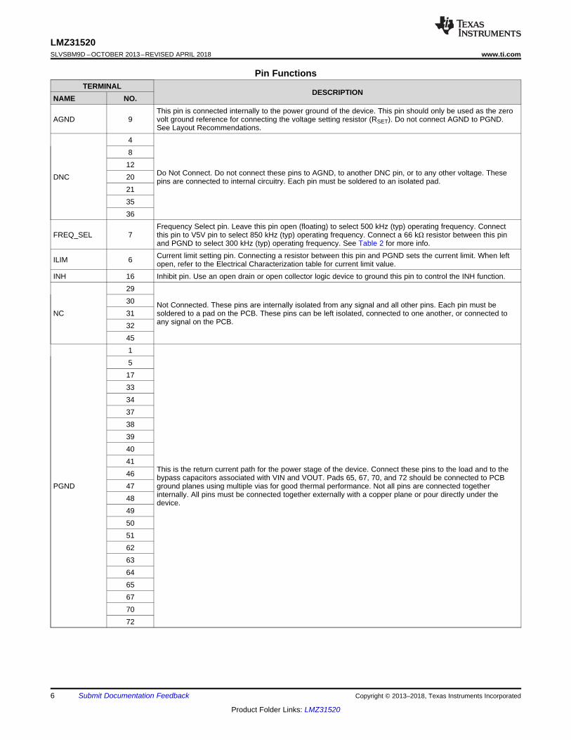
Functional Block Diagram
20
30
40
50
60
70
80
90
0 4 8 12 16 20
Am
bien
t Tem
pera
ture
(C
)
Output Current (A)
All Output Voltages
C001
Airflow = 100 LFM
0.0
1.0
2.0
3.0
4.0
5.0
6.0
0 4 8 12 16 20
Pow
er D
issi
patio
n (W
)
Output Current (A)
Vo = 3.3V, fsw = 500kHz Vo = 1.8V, fsw = 500kHz Vo = 1.2V, fsw = 500kHz Vo = 0.9V, fsw = 500kHz Vo = 0.6V, fsw = 500kHz
C004
20
30
40
50
60
70
80
90
0 4 8 12 16 20
Am
bien
t Tem
pera
ture
(C
)
Output Current (A)
9R9IVZ N+]
Vo = 3.3V, fsw = 500kHz
C001
Airflow = 0 LFM
30
40
50
60
70
80
90
100
0 4 8 12 16 20
Effi
cien
cy (
%)
Output Current (A)
Vo = 3.3V, fsw = 500kHz Vo = 1.8V, fsw = 500kHz Vo = 1.2V, fsw = 500kHz Vo = 0.9V, fsw = 500kHz Vo = 0.6V, fsw = 500kHz
C001
5
15
25
35
45
55
0 4 8 12 16 20
Out
put R
ippl
e V
olta
ge (
mV
)
Output Current (A)
Vo = 3.3V, fsw = 500kHz Vo = 1.8V, fsw = 500kHz Vo = 1.2V, fsw = 500kHz Vo = 0.9V, fsw = 500kHz Vo = 0.6V, fsw = 500kHz
C004
9
LMZ31520www.ti.com SLVSBM9D –OCTOBER 2013–REVISED APRIL 2018
Product Folder Links: LMZ31520
Submit Documentation FeedbackCopyright © 2013–2018, Texas Instruments Incorporated
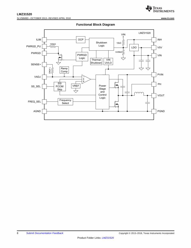
6 Typical Characteristics (PVIN = VIN = 12 V)The electrical characteristic data has been developed from actual products tested at 25°C. This data is considered typical forthe converter. Applies to Figure 1, Figure 2, and Figure 3. The temperature derating curves represent the conditions at whichinternal components are at or below the manufacturer's maximum operating temperatures. Derating limits apply to devicessoldered directly to a 100 mm × 100 mm six-layer PCB with 1 oz. copper. Applies to Figure 4 and Figure 5.
Figure 1. Efficiency vs. Output Current Figure 2. Voltage Ripple vs. Output Current
Figure 3. Power Dissipation vs. Output Current Figure 4. Safe Operating Area (0 LFM)
Figure 5. Safe Operating Area (100 LFM)
0.0
1.0
2.0
3.0
4.0
5.0
0 4 8 12 16 20
Pow
er D
issi
patio
n (W
)
Output Current (A)
Vo = 3.3V, fsw = 500kHz
Vo = 1.8V, fsw = 500kHz
Vo = 1.2V, fsw = 500kHz
Vo = 0.9V, fsw = 500kHz
Vo = 0.6V, fsw = 500kHz
C004
20
30
40
50
60
70
80
90
0 4 8 12 16 20
Am
bien
t Tem
pera
ture
(C
)
Output Current (A)
All Output Voltages
C001
Airflow = 0 LFM
30
40
50
60
70
80
90
100
0 4 8 12 16 20
Effi
cien
cy (
%)
Output Current (A)
Vo = 3.3V, fsw = 500kHz Vo = 1.8V, fsw = 500kHz Vo = 1.2V, fsw = 500kHz Vo = 0.9V, fsw = 500kHz Vo = 0.6V, fsw = 500kHz
C001
5
15
25
35
45
0 4 8 12 16 20
Out
put V
olta
ge R
ippl
e (m
V)
Output Current (A)
Vo = 3.3V, fsw = 500kHz
Vo = 1.8V, fsw = 500kHz
Vo = 1.2V, fsw = 500kHz
Vo = 0.9V, fsw = 500kHz
Vo = 0.6V, fsw = 500kHz
C004
10
LMZ31520SLVSBM9D –OCTOBER 2013–REVISED APRIL 2018 www.ti.com
Product Folder Links: LMZ31520
Submit Documentation Feedback Copyright © 2013–2018, Texas Instruments Incorporated
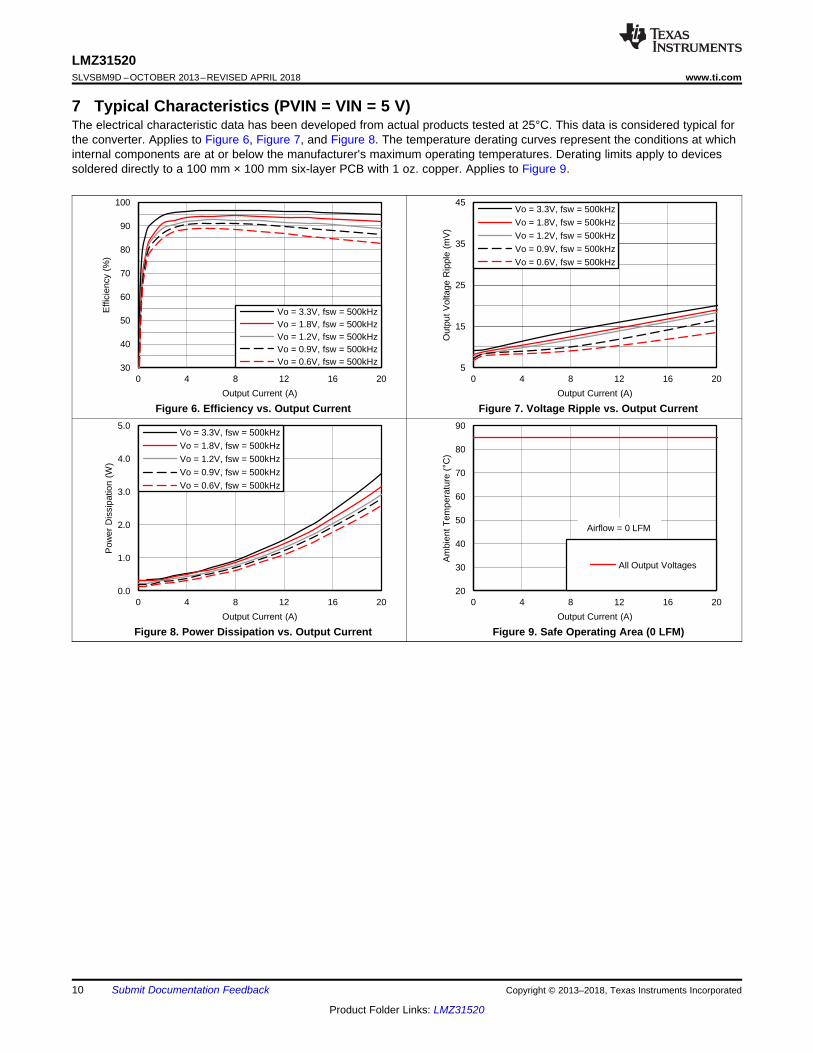
7 Typical Characteristics (PVIN = VIN = 5 V)The electrical characteristic data has been developed from actual products tested at 25°C. This data is considered typical forthe converter. Applies to Figure 6, Figure 7, and Figure 8. The temperature derating curves represent the conditions at whichinternal components are at or below the manufacturer's maximum operating temperatures. Derating limits apply to devicessoldered directly to a 100 mm × 100 mm six-layer PCB with 1 oz. copper. Applies to Figure 9.
Figure 6. Efficiency vs. Output Current Figure 7. Voltage Ripple vs. Output Current
Figure 8. Power Dissipation vs. Output Current Figure 9. Safe Operating Area (0 LFM)

11
LMZ31520www.ti.com SLVSBM9D –OCTOBER 2013–REVISED APRIL 2018
Product Folder Links: LMZ31520
Submit Documentation FeedbackCopyright © 2013–2018, Texas Instruments Incorporated
8 Application Information
8.1 Adjusting the Output VoltageThe VADJ control sets the output voltage of the LMZ31520. The output voltage adjustment range is from 0.6V to3.6V. The adjustment method requires the addition of RSET, which sets the output voltage, and the connection ofSENSE+ to VOUT. The RSET resistor must be connected directly between the VADJ (pin 13) and AGND (pin 9).The SENSE+ pin (pin 14) must be connected to VOUT either at the load for improved regulation or at VOUT ofthe device.
The LMZ31520 relies on a precision trimmed 0.6 V reference for the feedback voltage regulation and operates byregulating the valley of the voltage ripple appearing at the VADJ pin. The voltage ripple is a function of the inputvoltage and the output voltage, therefore the RSET resistor will change based on the input voltage. Table 1 givesthe calculated external RSET resistor for a number of common bus voltages for PVIN of 12 V, 5 V, and 3.3 V. Therecommended switching frequency is 500 kHz which can be configured by leaving the FREQ_SEL pin open. Toadjust the frequency, see Table 2.
Table 1. RSET Resistor ValuesRSET (Ω) RSET (Ω)
VOUT (V) PVIN = 12 V PVIN = 5 V PVIN = 3.3 V VOUT (V) PVIN = 12 V PVIN = 5 V PVIN = 3.3 V0.60 open open open 2.15 566 563 5600.65 18787 18681 18588 2.20 548 545 5420.70 9024 8993 8966 2.25 532 528 5250.75 5939 5923 5908 2.30 516 513 5100.80 4427 4416 4406 2.35 502 498 4950.85 3529 3521 3513 2.40 488 484 4810.90 2934 2927 2921 2.45 475 471 4680.95 2511 2505 2500 2.50 462 459 4561.00 2195 2190 2185 2.55 451 447 4441.05 1950 1945 1941 2.60 439 436 4331.10 1754 1749 1745 2.65 429 425 4221.15 1594 1589 1586 2.70 419 415 4121.20 1460 1456 1453 2.75 409 405 4021.25 1348 1344 1341 2.80 400 396 3931.30 1251 1248 1244 2.85 391 387 3841.35 1168 1164 1161 2.90 382 379 3751.40 1095 1091 1088 2.95 374 370 3671.45 1031 1027 1024 3.00 367 363 3591.50 973 970 968 3.05 359 355 3521.55 922 919 916 3.10 352 348 3451.60 876 873 870 3.15 345 341 3381.65 834 831 828 3.20 339 335 3311.70 797 793 790 3.25 332 328 3251.75 762 759 756 3.30 326 322 3181.80 730 727 724 3.35 320 316 3121.85 701 698 695 3.40 315 310 3071.90 674 671 668 3.45 309 305 3011.95 650 646 643 3.50 304 300 2962.00 626 623 620 3.55 299 294 2912.05 605 602 599 3.60 294 289 2862.10 585 581 578
12
LMZ31520SLVSBM9D –OCTOBER 2013–REVISED APRIL 2018 www.ti.com
Product Folder Links: LMZ31520
Submit Documentation Feedback Copyright © 2013–2018, Texas Instruments Incorporated
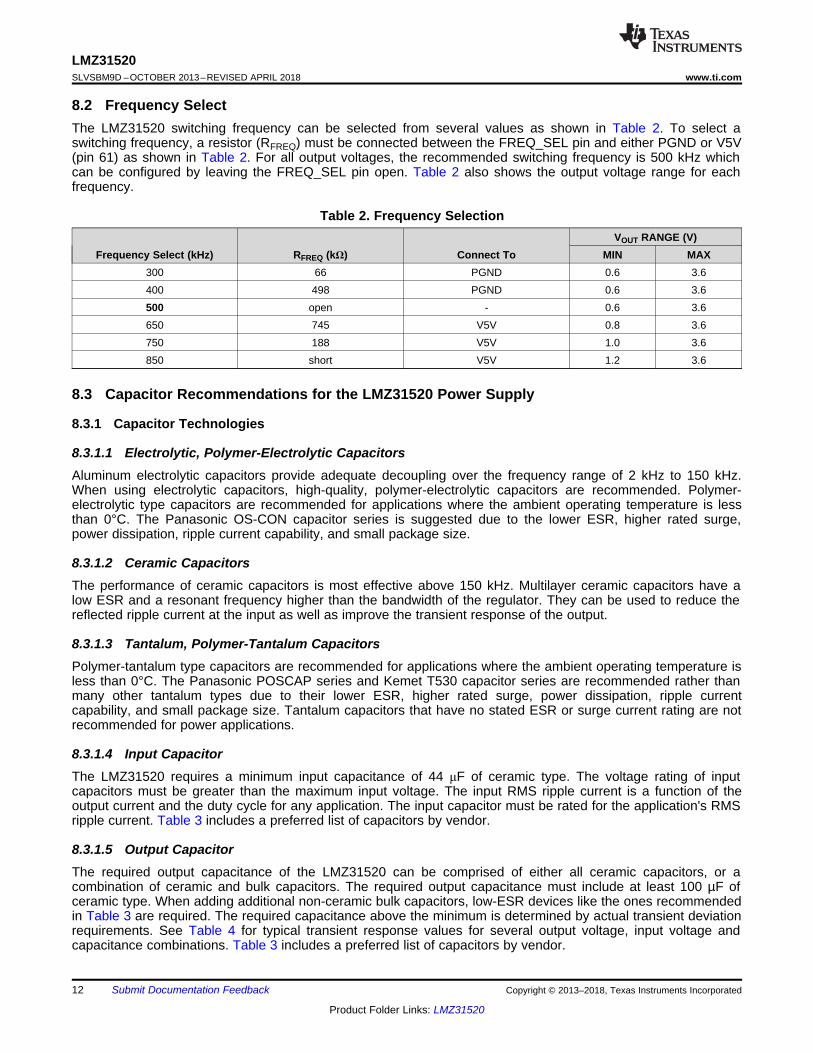
8.2 Frequency SelectThe LMZ31520 switching frequency can be selected from several values as shown in Table 2. To select aswitching frequency, a resistor (RFREQ) must be connected between the FREQ_SEL pin and either PGND or V5V(pin 61) as shown in Table 2. For all output voltages, the recommended switching frequency is 500 kHz whichcan be configured by leaving the FREQ_SEL pin open. Table 2 also shows the output voltage range for eachfrequency.
Table 2. Frequency Selection
Frequency Select (kHz) RFREQ (kΩ) Connect ToVOUT RANGE (V)
MIN MAX300 66 PGND 0.6 3.6400 498 PGND 0.6 3.6500 open - 0.6 3.6650 745 V5V 0.8 3.6750 188 V5V 1.0 3.6850 short V5V 1.2 3.6
8.3 Capacitor Recommendations for the LMZ31520 Power Supply
8.3.1 Capacitor Technologies
8.3.1.1 Electrolytic, Polymer-Electrolytic CapacitorsAluminum electrolytic capacitors provide adequate decoupling over the frequency range of 2 kHz to 150 kHz.When using electrolytic capacitors, high-quality, polymer-electrolytic capacitors are recommended. Polymer-electrolytic type capacitors are recommended for applications where the ambient operating temperature is lessthan 0°C. The Panasonic OS-CON capacitor series is suggested due to the lower ESR, higher rated surge,power dissipation, ripple current capability, and small package size.
8.3.1.2 Ceramic CapacitorsThe performance of ceramic capacitors is most effective above 150 kHz. Multilayer ceramic capacitors have alow ESR and a resonant frequency higher than the bandwidth of the regulator. They can be used to reduce thereflected ripple current at the input as well as improve the transient response of the output.
8.3.1.3 Tantalum, Polymer-Tantalum CapacitorsPolymer-tantalum type capacitors are recommended for applications where the ambient operating temperature isless than 0°C. The Panasonic POSCAP series and Kemet T530 capacitor series are recommended rather thanmany other tantalum types due to their lower ESR, higher rated surge, power dissipation, ripple currentcapability, and small package size. Tantalum capacitors that have no stated ESR or surge current rating are notrecommended for power applications.
8.3.1.4 Input CapacitorThe LMZ31520 requires a minimum input capacitance of 44 μF of ceramic type. The voltage rating of inputcapacitors must be greater than the maximum input voltage. The input RMS ripple current is a function of theoutput current and the duty cycle for any application. The input capacitor must be rated for the application's RMSripple current. Table 3 includes a preferred list of capacitors by vendor.
8.3.1.5 Output CapacitorThe required output capacitance of the LMZ31520 can be comprised of either all ceramic capacitors, or acombination of ceramic and bulk capacitors. The required output capacitance must include at least 100 µF ofceramic type. When adding additional non-ceramic bulk capacitors, low-ESR devices like the ones recommendedin Table 3 are required. The required capacitance above the minimum is determined by actual transient deviationrequirements. See Table 4 for typical transient response values for several output voltage, input voltage andcapacitance combinations. Table 3 includes a preferred list of capacitors by vendor.
13
LMZ31520www.ti.com SLVSBM9D –OCTOBER 2013–REVISED APRIL 2018
Product Folder Links: LMZ31520
Submit Documentation FeedbackCopyright © 2013–2018, Texas Instruments Incorporated
Capacitor Recommendations for the LMZ31520 Power Supply (continued)
(1) Capacitor Supplier Verification, RoHS, Lead-free and Material DetailsConsult capacitor suppliers regarding availability, material composition, RoHS and lead-free status, and manufacturing processrequirements for any capacitors identified in this table.
(2) Maximum ESR @ 100kHz, 25°C.
Table 3. Recommended Input/Output Capacitors (1)
VENDOR SERIES PART NUMBERCAPACITOR CHARACTERISTICS
WORKING VOLTAGE (V) CAPACITANCE (µF) ESR (2) (mΩ)
Murata X5R GRM32ER61E226K 25 22 2
TDK X5R C3216X5R1E476M 25 47 2
TDK X5R C3216X5R1C476M 16 47 2
Murata X5R GRM32ER61C476M 16 47 2
TDK X5R C3225X5R0J107M 6.3 100 2
Murata X5R GRM32ER60J107M 6.3 100 2
TDK X5R C3225X5R0J476K 6.3 47 2
Murata X5R GRM32ER60J476M 6.3 47 2
Panasonic EEH-ZA EEH-ZA1E101XP 25 100 30
Kemet T520 T520V107M010ASE025 10 100 25
Panasonic POSCAP 6TPE100MI 6.3 100 25
Panasonic POSCAP 2R5TPE220M7 2.5 220 7
Kemet T530 T530D227M006ATE006 6.3 220 6
Kemet T530 T530D337M006ATE010 6.3 330 10
Panasonic POSCAP 2TPF330M6 2.0 330 6
Panasonic POSCAP 6TPE330MFL 6.3 330 15
(1) Device configured for FCCM mode of operation, (pin 3 connected to pin 19).
8.4 Transient ResponseThe LMZ31520 is designed to have an ultra-fast load step response with minimal output capacitance. Table 4shows the voltage deviation and recovery time for several different transient conditions. Several transientwaveforms are shown in Application Curves (1).
Table 4. Output Voltage Transient ResponseCIN1 = 3 x 47 µF CERAMIC
VOUT (V) VIN (V) COUT1 Ceramic COUT2 BULKVOLTAGE DEVIATION (mV)
RECOVERY TIME(µs)5 A LOAD STEP,
(1 A/µs)10 A LOAD STEP,
(1 A/µs)
0.65 500 µF - 8 15 3512 500 µF - 8 15 35
0.95
500 µF - 8 15 40500 µF 470 µF 6 12 40
12500 µF - 8 20 40500 µF 470 µF 7 16 40
1.25
500 µF - 10 20 40500 µF 330 µF 8 15 40
12500 µF - 10 20 40500 µF 330 µF 8 16 40
1.85
500 µF - 10 20 40500 µF 330 µF 8 16 40
12500 µF - 10 20 40500 µF 330 µF 8 16 45
3.35 500 µF - 12 25 5012 500 µF - 12 25 50

14
LMZ31520SLVSBM9D –OCTOBER 2013–REVISED APRIL 2018 www.ti.com
Product Folder Links: LMZ31520
Submit Documentation Feedback Copyright © 2013–2018, Texas Instruments Incorporated
(1) Device configured for FCCM mode of operation, (pin 3 connected to pin 19).
8.5 Application Curves (1)
Figure 10. PVIN = 5V, VOUT = 1.8V, 5A Load Step Figure 11. PVIN = 5V, VOUT = 1.2V, 10A Load Step
Figure 12. PVIN = 12V, VOUT = 1.0V, 10A Load Step Figure 13. PVIN = 12V, VOUT = 1.8V, 10A Load Step

LMZ31520
PWRGD
SENSE+
VOUTPVIN
INH
FREQ_SEL
CIN2
22 µF
VADJ SS_SEL
AGND PGND
CIN1
100 µF
RSET
2.87 k
+
COUT1
3x 100 µF
COUT2
330 µF
VOUT
0.9 V
+
PVIN
3.3 V
CIN3
22 µF
VIN
4.5 V to 14.5 V
CIN3
4.7 µF
LMZ31520
PWRGD
SENSE+
VOUT
VIN
PVIN
INH
FREQ_SEL
CIN2
22 µF
VADJ SS_SEL
AGND PGND
CIN1
100 µF
RSET
1.43 k
+
COUT1
2x 100 µF
COUT2
220 µF
VOUT
1.2 V
+
VIN / PVIN
4.5 V to 14.5 V
CIN3
22 µF
15
LMZ31520www.ti.com SLVSBM9D –OCTOBER 2013–REVISED APRIL 2018
Product Folder Links: LMZ31520
Submit Documentation FeedbackCopyright © 2013–2018, Texas Instruments Incorporated
8.6 Application Schematics
Figure 14. Typical SchematicPVIN = VIN = 4.5 V to 14.5 V, VOUT = 1.2 V
Figure 15. Typical SchematicPVIN = 3.3 V, VIN = 4.5 V to 14.5 V, VOUT = 0.9 V

16
LMZ31520SLVSBM9D –OCTOBER 2013–REVISED APRIL 2018 www.ti.com
Product Folder Links: LMZ31520
Submit Documentation Feedback Copyright © 2013–2018, Texas Instruments Incorporated
8.7 Custom Design With WEBENCH® ToolsClick here to create a custom design using the LMZ31520 device with the WEBENCH® Power Designer.1. Start by entering the input voltage (VIN), output voltage (VOUT), and output current (IOUT) requirements.2. Optimize the design for key parameters such as efficiency, footprint, and cost using the optimizer dial.3. Compare the generated design with other possible solutions from Texas Instruments.
The WEBENCH Power Designer provides a customized schematic along with a list of materials with real-timepricing and component availability.
In most cases, these actions are available:• Run electrical simulations to see important waveforms and circuit performance• Run thermal simulations to understand board thermal performance• Export customized schematic and layout into popular CAD formats• Print PDF reports for the design, and share the design with colleagues
Get more information about WEBENCH tools at www.ti.com/WEBENCH.
8.8 VIN and PVIN Input VoltageThe LMZ31520 allows for a variety of applications by using the VIN and PVIN pins together or separately. TheVIN voltage supplies the internal control circuits of the device. The PVIN voltage provides the input voltage to thepower converter system.
If tied together, the input voltage for the VIN pin and the PVIN pin can range from 4.5 V to 14.5 V. If using theVIN pin separately from the PVIN pin, the VIN pin must be greater than 4.5 V, and the PVIN pin can range fromas low as 3.0 V to 14.5 V. When operating from a split rail, it is recommended to supply VIN from 5 V to 12 V, forbest performance.
8.9 3.3 V PVIN OperationApplications operating from a PVIN of 3.3 V must provide at least 4.5 V for VIN. It is recommended to supply VINfrom 5 V to 12 V, for best performance. See application note, SNVA692 for help creating 5 V from 3.3 V using asmall, simple charge pump device.
8.10 Power Good (PWRGD)The PWRGD pin is an open drain output. Once the voltage on the SENSE+ pin is between 90% and 115% of theset voltage, the PWRGD pin pull-down is released and the pin floats. The recommended pull-up resistor value isbetween 10 kΩ and 100 kΩ to a voltage source that is less than 7 V. An internal 100 kΩ pull-up resistor isprovided internal to the device between the PWRGD pin (pin 19) and PWRGD_PU pin (pin 18). ThePWRGD_PU pin can be connected to a voltage source less than 7 V or connected directly to V5V (pin 61), whichis an internal 5V regulator. The PWRGD pin is in a defined state once VIN is greater than 1.0 V. The PWRGDpin is pulled low when the voltage on SENSE+ is lower than 90% or greater than 115% of the nominal setvoltage. Also, the PWRGD pin is pulled low if the input UVLO or thermal shutdown is asserted or the INH pin ispulled low.

SS_SEL
PGND
RSS
PWRGD
SS_SEL
PGNDRSS
PWRGD
17
LMZ31520www.ti.com SLVSBM9D –OCTOBER 2013–REVISED APRIL 2018
Product Folder Links: LMZ31520
Submit Documentation FeedbackCopyright © 2013–2018, Texas Instruments Incorporated
8.11 Slow Start (SS_SEL)Connecting the SS_SEL pin to PWRGD or PGND sets the slow start interval of approximately 0.7 ms. Theconnection to either PWRGD or PGND determines the mode of the LMZ31520 as decribed in Auto-Skip Eco-mode™ / Forced Continuous Conduction Mode. Adding a resistor between SS_SEL pin and PWRGD or PGNDincreases the slow start time. Increasing the slow start time will reduce inrush current.Table 5 shows a resistorconnected between SS_SEL pin and PWRGD to select FCCM and Figure 17 shows a resistor between SS_SELpin and PGND to select Auto-skip mode. See Table 5 below for SS resistor values and timing interval.
Figure 16. Slow-Start Resistor (RSS) in FCCM Figure 17. Slow-Start Resistor (RSS) in Auto-skip Mode
Table 5. Slow-Start Resistor Values and Slow-Start TimeRSS (kΩ) short 61.9 161 436
SS Time (msec) 0.7 1.4 2.8 5.6
8.12 Auto-Skip Eco-mode™ / Forced Continuous Conduction ModeAuto-skip Eco-mode or Forced Continuous Conduction Mode (FCCM) can be selected using the SS_SEL pin(pin 3). Connect the SS_SEL pin to PGND to select Auto-skip Eco-mode or to the PWRGD pin to select FCCM.
In Auto-skip Eco-mode, the LMZ31520 automatically reduces the switching frequency at light load conditions tomaintain high efficiency. In FCCM, the controller keeps continuous conduction mode in light load condition andthe switching frequency is kept almost constant over the entire load range. Transient performance is best inFCCM.

18
LMZ31520SLVSBM9D –OCTOBER 2013–REVISED APRIL 2018 www.ti.com
Product Folder Links: LMZ31520
Submit Documentation Feedback Copyright © 2013–2018, Texas Instruments Incorporated
8.13 Power-Up CharacteristicsWhen configured as shown in the front page schematic, the LMZ31520 produces a regulated output voltagefollowing the application of a valid input voltage. During the power-up, internal soft-start circuitry slows the ratethat the output voltage rises, thereby limiting the amount of in-rush current that can be drawn from the inputsource. Figure 18 shows the start-up waveforms for a LMZ31520, operating from a 5-V input (PVIN=VIN) andwith the output voltage adjusted to 1.8 V. Figure 19 shows the start-up waveforms for a LMZ31520 starting upinto a pre-biased output voltage. The waveforms were measured with a 15-A constant current load.
Figure 18. Start-Up Waveforms Figure 19. Start-up into Pre-bias
8.14 Pre-Biased Start-UpThe LMZ31520 has been designed to prevent the low-side MOSFET from discharging a pre-biased output.During pre-biased startup, the low-side MOSFET does not turn on until the high-side MOSFET has startedswitching. The high-side MOSFET does not start switching until the slow start voltage exceeds the voltage on theVADJ pin. Refer to Figure 19.
8.15 Remote SenseThe SENSE+ pin must be connected to VOUT at the load, or at the device pins.
Connecting the SENSE+ pin to VOUT at the load improves the load regulation performance of the device byallowing it to compensate for any I-R voltage drop between its output pins and the load. An I-R drop is caused bythe high output current flowing through the small amount of pin and trace resistance. This should be limited to amaximum of 300 mV.
NOTEThe remote sense feature is not designed to compensate for the forward drop of nonlinearor frequency dependent components that may be placed in series with the converteroutput. Examples include OR-ing diodes, filter inductors, ferrite beads, and fuses. Whenthese components are enclosed by the SENSE+ connection, they are effectively placedinside the regulation control loop, which can adversely affect the stability of the regulator.

INH
PGND
Q1
INH
Control
19
LMZ31520www.ti.com SLVSBM9D –OCTOBER 2013–REVISED APRIL 2018
Product Folder Links: LMZ31520
Submit Documentation FeedbackCopyright © 2013–2018, Texas Instruments Incorporated
8.16 Output On/Off Inhibit (INH)The INH pin provides electrical on/off control of the device. Once the INH pin voltage exceeds the thresholdvoltage, the device starts operation. If the INH pin voltage is pulled below the threshold voltage, the regulatorstops switching and enters low quiescent current state.
The INH pin has an internal pull-up current source, allowing the user to float the INH pin for enabling the device.If an application requires controlling the INH pin, use an open drain/collector device, or a suitable logic gate tointerface with the pin.
Figure 20 shows the typical application of the inhibit function. The Inhibit control has its own internal pull-up toVIN potential. An open-collector or open-drain device is recommended to control this input.
Turning Q1 on applies a low voltage to the inhibit control (INH) pin and disables the output of the supply, shownin Figure 21. If Q1 is turned off, the supply executes a soft-start power-up sequence, as shown in Figure 22. Aregulated output voltage is produced within 2 ms. The waveforms were measured with a 5-A constant currentload.
Figure 20. Typical Inhibit Control
Figure 21. Inhibit Turn-Off Figure 22. Inhibit Turn-On
20
LMZ31520SLVSBM9D –OCTOBER 2013–REVISED APRIL 2018 www.ti.com
Product Folder Links: LMZ31520
Submit Documentation Feedback Copyright © 2013–2018, Texas Instruments Incorporated
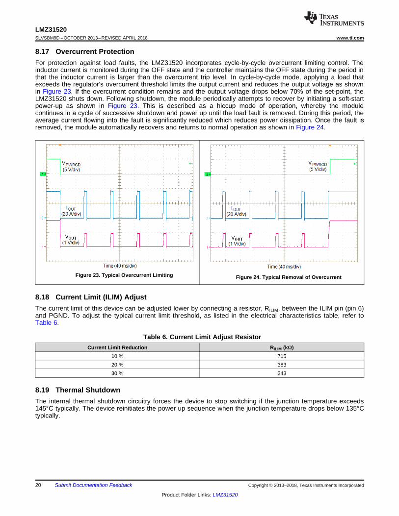
8.17 Overcurrent ProtectionFor protection against load faults, the LMZ31520 incorporates cycle-by-cycle overcurrent limiting control. Theinductor current is monitored during the OFF state and the controller maintains the OFF state during the period inthat the inductor current is larger than the overcurrent trip level. In cycle-by-cycle mode, applying a load thatexceeds the regulator's overcurrent threshold limits the output current and reduces the output voltage as shownin Figure 23. If the overcurrent condition remains and the output voltage drops below 70% of the set-point, theLMZ31520 shuts down. Following shutdown, the module periodically attempts to recover by initiating a soft-startpower-up as shown in Figure 23. This is described as a hiccup mode of operation, whereby the modulecontinues in a cycle of successive shutdown and power up until the load fault is removed. During this period, theaverage current flowing into the fault is significantly reduced which reduces power dissipation. Once the fault isremoved, the module automatically recovers and returns to normal operation as shown in Figure 24.
Figure 23. Typical Overcurrent Limiting Figure 24. Typical Removal of Overcurrent
8.18 Current Limit (ILIM) AdjustThe current limit of this device can be adjusted lower by connecting a resistor, RILIM, between the ILIM pin (pin 6)and PGND. To adjust the typical current limit threshold, as listed in the electrical characteristics table, refer toTable 6.
Table 6. Current Limit Adjust ResistorCurrent Limit Reduction RILIM (kΩ)
10 % 71520 % 38330 % 243
8.19 Thermal ShutdownThe internal thermal shutdown circuitry forces the device to stop switching if the junction temperature exceeds145°C typically. The device reinitiates the power up sequence when the junction temperature drops below 135°Ctypically.
21
LMZ31520www.ti.com SLVSBM9D –OCTOBER 2013–REVISED APRIL 2018
Product Folder Links: LMZ31520
Submit Documentation FeedbackCopyright © 2013–2018, Texas Instruments Incorporated
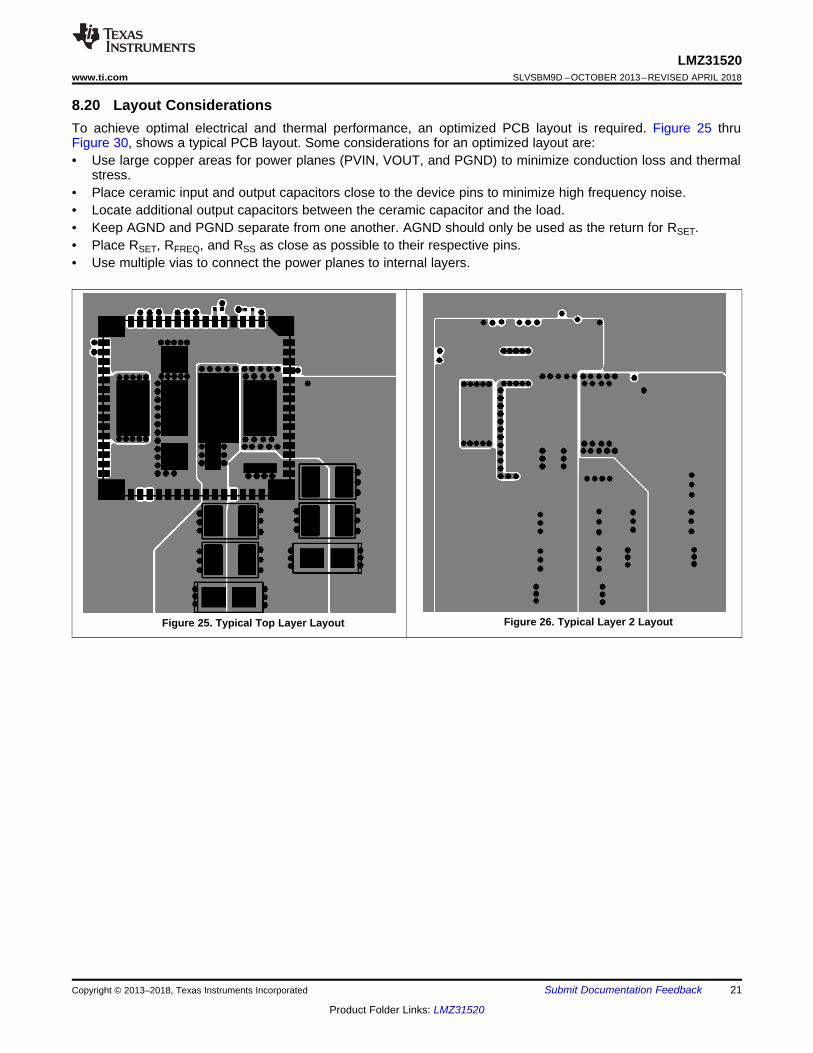
8.20 Layout ConsiderationsTo achieve optimal electrical and thermal performance, an optimized PCB layout is required. Figure 25 thruFigure 30, shows a typical PCB layout. Some considerations for an optimized layout are:• Use large copper areas for power planes (PVIN, VOUT, and PGND) to minimize conduction loss and thermal
stress.• Place ceramic input and output capacitors close to the device pins to minimize high frequency noise.• Locate additional output capacitors between the ceramic capacitor and the load.• Keep AGND and PGND separate from one another. AGND should only be used as the return for RSET.• Place RSET, RFREQ, and RSS as close as possible to their respective pins.• Use multiple vias to connect the power planes to internal layers.
Figure 25. Typical Top Layer Layout Figure 26. Typical Layer 2 Layout

22
LMZ31520SLVSBM9D –OCTOBER 2013–REVISED APRIL 2018 www.ti.com
Product Folder Links: LMZ31520
Submit Documentation Feedback Copyright © 2013–2018, Texas Instruments Incorporated
Layout Considerations (continued)
Figure 27. Typical Layer 3 Layout Figure 28. Typical Layer 4 Layout
Figure 29. Typical Layer 5 Layout Figure 30. Typical Bottom Layer Layout

23
LMZ31520www.ti.com SLVSBM9D –OCTOBER 2013–REVISED APRIL 2018
Product Folder Links: LMZ31520
Submit Documentation FeedbackCopyright © 2013–2018, Texas Instruments Incorporated
8.21 EMIThe LMZ31520 is compliant with EN55022 Class A radiated emissions. Figure 31 and Figure 32 show typicalexamples of radiated emissions plots for the LMZ31520 operating from 5V and 12V respectively. Both graphsinclude the plots of the antenna in the horizontal and vertical positions.
Figure 31. Radiated Emissions 5-V Input, 1.8-V Output, 20-A Load (EN55022 Class A)
Figure 32. Radiated Emissions 12-V Input, 3.3-V Output,20-A Load (EN55022 Class A)

24
LMZ31520SLVSBM9D –OCTOBER 2013–REVISED APRIL 2018 www.ti.com
Product Folder Links: LMZ31520
Submit Documentation Feedback Copyright © 2013–2018, Texas Instruments Incorporated
9 Revision HistoryNOTE: Page numbers for previous revisions may differ from page numbers in the current version.
Changes from Revision C (June 2017) to Revision D Page
• Added WEBENCH® design links for the LMZ31520.............................................................................................................. 1• Increased the peak reflow temperature and maximum number of reflows to JEDEC specifications for improved
manufacturability..................................................................................................................................................................... 2• Added Device Support section ............................................................................................................................................. 25• Added Mechanical, Packaging, and Orderable Information section .................................................................................... 26
Changes from Revision B (December 2013) to Revision C Page
• Added peak reflow and maximum number of reflows information ........................................................................................ 2
Changes from Revision A (December 2013) to Revision B Page
• Added additional capacitors to the recommended capacitor table....................................................................................... 13
Changes from Original (October 2013) to Revision A Page
• Changed status from Preview to Production .......................................................................................................................... 1

25
LMZ31520www.ti.com SLVSBM9D –OCTOBER 2013–REVISED APRIL 2018
Product Folder Links: LMZ31520
Submit Documentation FeedbackCopyright © 2013–2018, Texas Instruments Incorporated
10 Device and Documentation Support
10.1 Device Support
10.1.1 Development Support
10.1.1.1 Custom Design With WEBENCH® ToolsClick here to create a custom design using the LMZ31520 device with the WEBENCH® Power Designer.1. Start by entering the input voltage (VIN), output voltage (VOUT), and output current (IOUT) requirements.2. Optimize the design for key parameters such as efficiency, footprint, and cost using the optimizer dial.3. Compare the generated design with other possible solutions from Texas Instruments.
The WEBENCH Power Designer provides a customized schematic along with a list of materials with real-timepricing and component availability.
In most cases, these actions are available:• Run electrical simulations to see important waveforms and circuit performance• Run thermal simulations to understand board thermal performance• Export customized schematic and layout into popular CAD formats• Print PDF reports for the design, and share the design with colleagues
Get more information about WEBENCH tools at www.ti.com/WEBENCH.
10.2 Documentation Support
10.2.1 Related DocumentationFor related documentation see the following:
Soldering Requirements for BQFN Packages
10.3 Receiving Notification of Documentation UpdatesTo receive notification of documentation updates, navigate to the device product folder on ti.com. In the upperright corner, click on Alert me to register and receive a weekly digest of any product information that haschanged. For change details, review the revision history included in any revised document.
10.4 Community ResourcesThe following links connect to TI community resources. Linked contents are provided "AS IS" by the respectivecontributors. They do not constitute TI specifications and do not necessarily reflect TI's views; see TI's Terms ofUse.
TI E2E™ Online Community TI's Engineer-to-Engineer (E2E) Community. Created to foster collaborationamong engineers. At e2e.ti.com, you can ask questions, share knowledge, explore ideas and helpsolve problems with fellow engineers.
Design Support TI's Design Support Quickly find helpful E2E forums along with design support tools andcontact information for technical support.
10.5 TrademarksEco-mode, E2E are trademarks of Texas Instruments.WEBENCH is a registered trademark of Texas Instruments.All other trademarks are the property of their respective owners.
10.6 Electrostatic Discharge CautionThis integrated circuit can be damaged by ESD. Texas Instruments recommends that all integrated circuits be handled withappropriate precautions. Failure to observe proper handling and installation procedures can cause damage.
ESD damage can range from subtle performance degradation to complete device failure. Precision integrated circuits may be moresusceptible to damage because very small parametric changes could cause the device not to meet its published specifications.

26
LMZ31520SLVSBM9D –OCTOBER 2013–REVISED APRIL 2018 www.ti.com
Product Folder Links: LMZ31520
Submit Documentation Feedback Copyright © 2013–2018, Texas Instruments Incorporated
10.7 GlossarySLYZ022 — TI Glossary.
This glossary lists and explains terms, acronyms, and definitions.
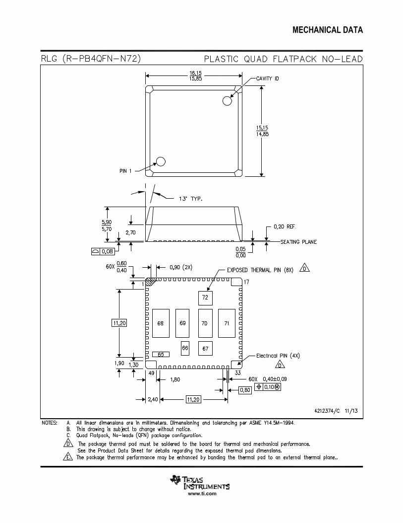
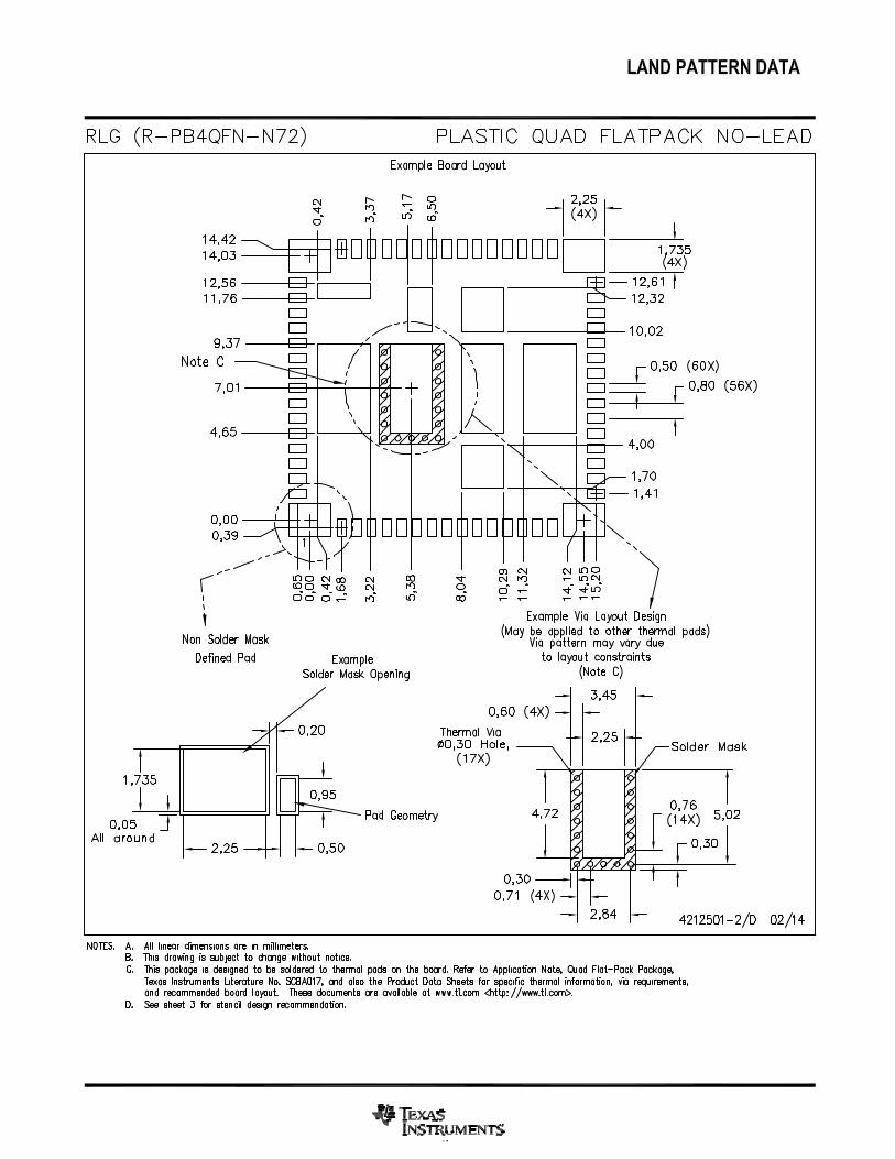
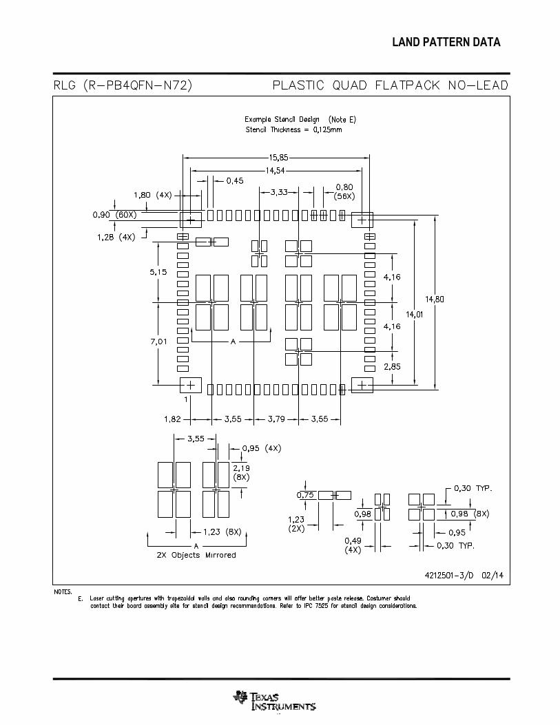
11 Mechanical, Packaging, and Orderable InformationThe following pages include mechanical, packaging, and orderable information. This information is the mostcurrent data available for the designated devices. This data is subject to change without notice and revision ofthis document. For browser-based versions of this data sheet, refer to the left-hand navigation.

PACKAGE OPTION ADDENDUM
www.ti.com 25-Jun-2018
Addendum-Page 1
PACKAGING INFORMATION
Orderable Device Status(1)
Package Type PackageDrawing
Pins PackageQty
Eco Plan(2)
Lead/Ball Finish(6)
MSL Peak Temp(3)
Op Temp (°C) Device Marking(4/5)
Samples
LMZ31520RLGT ACTIVE BQFN RLG 72 250 RoHS (InWork) & Green
(In Work)
CU NIPDAU Level-3-245C-168 HR -40 to 85 (53353DQP, LMZ3152 0)
(1) The marketing status values are defined as follows:ACTIVE: Product device recommended for new designs.LIFEBUY: TI has announced that the device will be discontinued, and a lifetime-buy period is in effect.NRND: Not recommended for new designs. Device is in production to support existing customers, but TI does not recommend using this part in a new design.PREVIEW: Device has been announced but is not in production. Samples may or may not be available.OBSOLETE: TI has discontinued the production of the device.
(2) RoHS: TI defines "RoHS" to mean semiconductor products that are compliant with the current EU RoHS requirements for all 10 RoHS substances, including the requirement that RoHS substancedo not exceed 0.1% by weight in homogeneous materials. Where designed to be soldered at high temperatures, "RoHS" products are suitable for use in specified lead-free processes. TI mayreference these types of products as "Pb-Free".RoHS Exempt: TI defines "RoHS Exempt" to mean products that contain lead but are compliant with EU RoHS pursuant to a specific EU RoHS exemption.Green: TI defines "Green" to mean the content of Chlorine (Cl) and Bromine (Br) based flame retardants meet JS709B low halogen requirements of <=1000ppm threshold. Antimony trioxide basedflame retardants must also meet the <=1000ppm threshold requirement.
(3) MSL, Peak Temp. - The Moisture Sensitivity Level rating according to the JEDEC industry standard classifications, and peak solder temperature.
(4) There may be additional marking, which relates to the logo, the lot trace code information, or the environmental category on the device.
(5) Multiple Device Markings will be inside parentheses. Only one Device Marking contained in parentheses and separated by a "~" will appear on a device. If a line is indented then it is a continuationof the previous line and the two combined represent the entire Device Marking for that device.
(6) Lead/Ball Finish - Orderable Devices may have multiple material finish options. Finish options are separated by a vertical ruled line. Lead/Ball Finish values may wrap to two lines if the finishvalue exceeds the maximum column width.
Important Information and Disclaimer:The information provided on this page represents TI's knowledge and belief as of the date that it is provided. TI bases its knowledge and belief on informationprovided by third parties, and makes no representation or warranty as to the accuracy of such information. Efforts are underway to better integrate information from third parties. TI has taken andcontinues to take reasonable steps to provide representative and accurate information but may not have conducted destructive testing or chemical analysis on incoming materials and chemicals.TI and TI suppliers consider certain information to be proprietary, and thus CAS numbers and other limited information may not be available for release.
In no event shall TI's liability arising out of such information exceed the total purchase price of the TI part(s) at issue in this document sold by TI to Customer on an annual basis.


IMPORTANT NOTICE
Texas Instruments Incorporated (TI) reserves the right to make corrections, enhancements, improvements and other changes to itssemiconductor products and services per JESD46, latest issue, and to discontinue any product or service per JESD48, latest issue. Buyersshould obtain the latest relevant information before placing orders and should verify that such information is current and complete.TI’s published terms of sale for semiconductor products (http://www.ti.com/sc/docs/stdterms.htm) apply to the sale of packaged integratedcircuit products that TI has qualified and released to market. Additional terms may apply to the use or sale of other types of TI products andservices.Reproduction of significant portions of TI information in TI data sheets is permissible only if reproduction is without alteration and isaccompanied by all associated warranties, conditions, limitations, and notices. TI is not responsible or liable for such reproduceddocumentation. Information of third parties may be subject to additional restrictions. Resale of TI products or services with statementsdifferent from or beyond the parameters stated by TI for that product or service voids all express and any implied warranties for theassociated TI product or service and is an unfair and deceptive business practice. TI is not responsible or liable for any such statements.Buyers and others who are developing systems that incorporate TI products (collectively, “Designers”) understand and agree that Designersremain responsible for using their independent analysis, evaluation and judgment in designing their applications and that Designers havefull and exclusive responsibility to assure the safety of Designers' applications and compliance of their applications (and of all TI productsused in or for Designers’ applications) with all applicable regulations, laws and other applicable requirements. Designer represents that, withrespect to their applications, Designer has all the necessary expertise to create and implement safeguards that (1) anticipate dangerousconsequences of failures, (2) monitor failures and their consequences, and (3) lessen the likelihood of failures that might cause harm andtake appropriate actions. Designer agrees that prior to using or distributing any applications that include TI products, Designer willthoroughly test such applications and the functionality of such TI products as used in such applications.TI’s provision of technical, application or other design advice, quality characterization, reliability data or other services or information,including, but not limited to, reference designs and materials relating to evaluation modules, (collectively, “TI Resources”) are intended toassist designers who are developing applications that incorporate TI products; by downloading, accessing or using TI Resources in anyway, Designer (individually or, if Designer is acting on behalf of a company, Designer’s company) agrees to use any particular TI Resourcesolely for this purpose and subject to the terms of this Notice.TI’s provision of TI Resources does not expand or otherwise alter TI’s applicable published warranties or warranty disclaimers for TIproducts, and no additional obligations or liabilities arise from TI providing such TI Resources. TI reserves the right to make corrections,enhancements, improvements and other changes to its TI Resources. TI has not conducted any testing other than that specificallydescribed in the published documentation for a particular TI Resource.Designer is authorized to use, copy and modify any individual TI Resource only in connection with the development of applications thatinclude the TI product(s) identified in such TI Resource. NO OTHER LICENSE, EXPRESS OR IMPLIED, BY ESTOPPEL OR OTHERWISETO ANY OTHER TI INTELLECTUAL PROPERTY RIGHT, AND NO LICENSE TO ANY TECHNOLOGY OR INTELLECTUAL PROPERTYRIGHT OF TI OR ANY THIRD PARTY IS GRANTED HEREIN, including but not limited to any patent right, copyright, mask work right, orother intellectual property right relating to any combination, machine, or process in which TI products or services are used. Informationregarding or referencing third-party products or services does not constitute a license to use such products or services, or a warranty orendorsement thereof. Use of TI Resources may require a license from a third party under the patents or other intellectual property of thethird party, or a license from TI under the patents or other intellectual property of TI.TI RESOURCES ARE PROVIDED “AS IS” AND WITH ALL FAULTS. TI DISCLAIMS ALL OTHER WARRANTIES ORREPRESENTATIONS, EXPRESS OR IMPLIED, REGARDING RESOURCES OR USE THEREOF, INCLUDING BUT NOT LIMITED TOACCURACY OR COMPLETENESS, TITLE, ANY EPIDEMIC FAILURE WARRANTY AND ANY IMPLIED WARRANTIES OFMERCHANTABILITY, FITNESS FOR A PARTICULAR PURPOSE, AND NON-INFRINGEMENT OF ANY THIRD PARTY INTELLECTUALPROPERTY RIGHTS. TI SHALL NOT BE LIABLE FOR AND SHALL NOT DEFEND OR INDEMNIFY DESIGNER AGAINST ANY CLAIM,INCLUDING BUT NOT LIMITED TO ANY INFRINGEMENT CLAIM THAT RELATES TO OR IS BASED ON ANY COMBINATION OFPRODUCTS EVEN IF DESCRIBED IN TI RESOURCES OR OTHERWISE. IN NO EVENT SHALL TI BE LIABLE FOR ANY ACTUAL,DIRECT, SPECIAL, COLLATERAL, INDIRECT, PUNITIVE, INCIDENTAL, CONSEQUENTIAL OR EXEMPLARY DAMAGES INCONNECTION WITH OR ARISING OUT OF TI RESOURCES OR USE THEREOF, AND REGARDLESS OF WHETHER TI HAS BEENADVISED OF THE POSSIBILITY OF SUCH DAMAGES.Unless TI has explicitly designated an individual product as meeting the requirements of a particular industry standard (e.g., ISO/TS 16949and ISO 26262), TI is not responsible for any failure to meet such industry standard requirements.Where TI specifically promotes products as facilitating functional safety or as compliant with industry functional safety standards, suchproducts are intended to help enable customers to design and create their own applications that meet applicable functional safety standardsand requirements. Using products in an application does not by itself establish any safety features in the application. Designers mustensure compliance with safety-related requirements and standards applicable to their applications. Designer may not use any TI products inlife-critical medical equipment unless authorized officers of the parties have executed a special contract specifically governing such use.Life-critical medical equipment is medical equipment where failure of such equipment would cause serious bodily injury or death (e.g., lifesupport, pacemakers, defibrillators, heart pumps, neurostimulators, and implantables). Such equipment includes, without limitation, allmedical devices identified by the U.S. Food and Drug Administration as Class III devices and equivalent classifications outside the U.S.TI may expressly designate certain products as completing a particular qualification (e.g., Q100, Military Grade, or Enhanced Product).Designers agree that it has the necessary expertise to select the product with the appropriate qualification designation for their applicationsand that proper product selection is at Designers’ own risk. Designers are solely responsible for compliance with all legal and regulatoryrequirements in connection with such selection.Designer will fully indemnify TI and its representatives against any damages, costs, losses, and/or liabilities arising out of Designer’s non-compliance with the terms and provisions of this Notice.
Mailing Address: Texas Instruments, Post Office Box 655303, Dallas, Texas 75265Copyright © 2018, Texas Instruments Incorporated
Related Documents