www.ti.com FEATURES APPLICATIONS L . . . DBV (SOT -23-5) OR DCK (SC-70) ACKAGE (T OP VIEW) 1 2 3 5 4 IN+ V C C - IN- V C C + OUTPUT LMV932 . . . D (SOIC) OR DGK (VSSO ACKAGE (T OP VIEW) LMV . . . D (SOIC) OR PW ACKAGE (T OP VIEW) 1 2 3 4 5 6 7 14 13 12 1 1 10 9 8 1OUT 1IN- 1IN+ V C C + 2IN+ 2IN- 2OUT 4OUT 4IN- 4IN+ V C C - 3IN+ 3IN- 3OUT 1 2 3 4 8 7 6 5 1OUT 1IN- 1IN+ V C C - V C C + 2OUT 2IN- 2IN+ DESCRIPTION/ORDERING INFORMATION LMV931 SINGLE, LMV932 DUAL, LMV934 QUAD 1.8-V OPERATIONAL AMPLIFIERS WITH RAIL-TO-RAIL INPUT AND OUTPUT SLOS441G – AUGUST 2004 – REVISED FEBRUARY 2006 • 1.8-V, 2.7-V, and 5-V Specifications • Rail-to-Rail Output Swing – 600-Ω Load . . . 80 mV From Rail – 2-kΩ Load . . . 30 mV From Rail • V ICR . . . 200 mV Beyond Rails • Gain Bandwidth . . . 1.4 MHz • Supply Current . . . 100 μA/Amplifier • Max V IO . . . 4 mV • Space-Saving Packages – LMV931: SOT-23 and SC-70 – LMV932: MSOP and SOIC – LMV934: SOIC and TSSOP • Industrial (Utility/Energy Metering) • Automotive • Communications (Optical Telecom, Data/Voice Cable Modems) • Consumer Electronics (PDAs, PCs, CDR/W, Portable Audio) • Supply-Current Monitoring • Battery Monitoring XXX ORDERING INFORMATION T A PACKAGE (1) ORDERABLE PART NUMBER TOP-SIDE MARKING (2) Reel of 3000 LMV931IDBVR RBB_ SOT-23 – DBV Reel of 250 LMV931IDBVT PREVIEW Single Reel of 3000 LMV931IDCKR RB_ SC-70 – DCK Reel of 250 LMV931IDCKT PREVIEW Reel of 2500 LMV932IDGKR RD_ MSOP/VSSOP – DGK Reel of 250 LMV932IDGKT PREVIEW –40°C to 125°C Dual Tube of 75 LMV932ID SOIC – D MV932I Reel of 2500 LMV932IDR Tube of 50 LMV934ID SOIC – D LMV934I Reel of 2500 LMV934IDR Quad Tube of 90 LMV934IPW TSSOP – PW MV934I Reel of 2000 LMV934IPWR (1) Package drawings, standard packing quantities, thermal data, symbolization, and PCB design guidelines are available at www.ti.com/sc/package. (2) DBV/DCK/DGK: The actual top-side marking has one additional character that designates the assembly/test site. Please be aware that an important notice concerning availability, standard warranty, and use in critical applications of Texas Instruments semiconductor products and disclaimers thereto appears at the end of this data sheet. PRODUCTION DATA information is current as of publication date. Copyright © 2004–2006, Texas Instruments Incorporated Products conform to specifications per the terms of the Texas Instruments standard warranty. Production processing does not necessarily include testing of all parameters. www.BDTIC.com/TI

Welcome message from author
This document is posted to help you gain knowledge. Please leave a comment to let me know what you think about it! Share it to your friends and learn new things together.
Transcript

www.ti.com
FEATURES
APPLICATIONS
LMV931 . . . DBV (SOT -23-5) OR DCK (SC-70) P ACKAGE(T OP VIEW)
1
2
3
5
4
IN+VCC−
IN−
VCC+
OUTPUT
LMV932 . . . D (SOIC) ORDGK (VSSOP/MSOP) P ACKAGE
(T OP VIEW)
LMV934 . . . D (SOIC) OR PW (TSSOP) P ACKAGE(T OP VIEW)
1
2
3
4
5
6
7
14
13
12
11
10
9
8
1OUT1IN−1IN+VCC+2IN+2IN−
2OUT
4OUT4IN−4IN+VCC−3IN+3IN−3OUT
1
2
3
4
8
7
6
5
1OUT1IN−1IN+VCC−
VCC+2OUT2IN−2IN+
DESCRIPTION/ORDERING INFORMATION
LMV931 SINGLE,, LMV932 DUAL,, LMV934 QUAD1.8-V OPERATIONAL AMPLIFIERS
WITH RAIL-TO-RAIL INPUT AND OUTPUTSLOS441G–AUGUST 2004–REVISED FEBRUARY 2006
• 1.8-V, 2.7-V, and 5-V Specifications• Rail-to-Rail Output Swing
– 600-Ω Load . . . 80 mV From Rail– 2-kΩ Load . . . 30 mV From Rail
• VICR . . . 200 mV Beyond Rails• Gain Bandwidth . . . 1.4 MHz• Supply Current . . . 100 µA/Amplifier• Max VIO . . . 4 mV• Space-Saving Packages
– LMV931: SOT-23 and SC-70– LMV932: MSOP and SOIC– LMV934: SOIC and TSSOP
• Industrial (Utility/Energy Metering)• Automotive• Communications (Optical Telecom, Data/Voice
Cable Modems)• Consumer Electronics (PDAs, PCs, CDR/W,
Portable Audio)• Supply-Current Monitoring• Battery Monitoring
XXX
ORDERING INFORMATION
TA PACKAGE (1) ORDERABLE PART NUMBER TOP-SIDE MARKING (2)
Reel of 3000 LMV931IDBVR RBB_SOT-23 – DBV
Reel of 250 LMV931IDBVT PREVIEWSingle
Reel of 3000 LMV931IDCKR RB_SC-70 – DCK
Reel of 250 LMV931IDCKT PREVIEW
Reel of 2500 LMV932IDGKR RD_MSOP/VSSOP – DGK
Reel of 250 LMV932IDGKT PREVIEW–40°C to 125°C Dual
Tube of 75 LMV932IDSOIC – D MV932I
Reel of 2500 LMV932IDR
Tube of 50 LMV934IDSOIC – D LMV934I
Reel of 2500 LMV934IDRQuad
Tube of 90 LMV934IPWTSSOP – PW MV934I
Reel of 2000 LMV934IPWR
(1) Package drawings, standard packing quantities, thermal data, symbolization, and PCB design guidelines are available atwww.ti.com/sc/package.
(2) DBV/DCK/DGK: The actual top-side marking has one additional character that designates the assembly/test site.
Please be aware that an important notice concerning availability, standard warranty, and use in critical applications of TexasInstruments semiconductor products and disclaimers thereto appears at the end of this data sheet.
PRODUCTION DATA information is current as of publication date. Copyright © 2004–2006, Texas Instruments IncorporatedProducts conform to specifications per the terms of the TexasInstruments standard warranty. Production processing does notnecessarily include testing of all parameters.www.BDTIC.com/TI

www.ti.com
DESCRIPTION/ORDERING INFORMATION (CONTINUED)
IN+IN−
VBIAS1
Class ABControl
VCC+
OUT
VCC−
Q1Q4
Q3
Q2
M3 M4
I4I3
M7 M8 M8
M6M5
I2I1
M2M1
VBIAS2
IP
IN
LMV931 SINGLE,, LMV932 DUAL,, LMV934 QUAD1.8-V OPERATIONAL AMPLIFIERSWITH RAIL-TO-RAIL INPUT AND OUTPUTSLOS441G–AUGUST 2004–REVISED FEBRUARY 2006
The LMV93x devices are low-voltage low-power operational amplifiers that are well suited for today's low-voltageand/or portable applications. Specified for operation of 1.8 V to 5 V, they can be used in portable applicationsthat are powered from a single-cell Li-ion or two-cell batteries. They have rail-to-rail input and output capability formaximum signal swings in low-voltage applications. The LMV93x input common-mode voltage extends 200 mVbeyond the rails for increased flexibility. The output can swing rail-to-rail unloaded and typically can reach 80 mVfrom the rails, while driving a 600-Ω load (at 1.8-V operation).
During 1.8-V operation, the devices typically consume a quiescent current of 103 µA per channel, and yet theyare able to achieve excellent electrical specifications, such as 101-dB open-loop DC gain and 1.4-MHz gainbandwidth. Furthermore, the amplifiers offer good output drive characteristics, with the ability to drive a 600-Ωload and 1000-pF capacitance with minimal ringing.
The LMV93x devices are offered in the latest packaging technology to meet the most demandingspace-constraint applications. The LMV931 is offered in standard SOT-23 and SC-70 packages. The LMV932 isavailable in the traditional MSOP and SOIC packages. The LMV934 is available in the traditional SOIC andTSSOP packages.
The LMV93x devices are characterized for operation from –40°C to 125°C, making the part universally suited forcommercial, industrial, and automotive applications.
SIMPLIFIED SCHEMATIC
2 Submit Documentation Feedbackwww.BDTIC.com/TI

www.ti.com
Absolute Maximum Ratings (1)
Recommended Operating Conditions
ESD Protection
LMV931 SINGLE,, LMV932 DUAL,, LMV934 QUAD1.8-V OPERATIONAL AMPLIFIERS
WITH RAIL-TO-RAIL INPUT AND OUTPUTSLOS441G–AUGUST 2004–REVISED FEBRUARY 2006
over free-air temperature range (unless otherwise noted)
MIN MAX UNIT
VCC+ – VCC– Supply voltage (2) 5.5 V
VID Differential input voltage (3) Supply voltage
VI Input voltage range, either input VCC– – 0.2 VCC+ + 0.2 V
Duration of output short circuit (one amplifier) to VCC±(4) (5) Unlimited
D package (8 pin) 97
D package (14 pin) 86
DBV package 206θJA Package thermal impedance (5) (6) °C/W
DCK package 252
DGK package 172
PW package 113
TJ Operating virtual junction temperature 150 °C
Tstg Storage temperature range –65 150 °C
(1) Stresses beyond those listed under Absolute Maximum Ratings may cause permanent damage to the device. These are stress ratingsonly, and functional operation of the device at these or any other conditions beyond those indicated under Recommended OperatingConditions is not implied. Exposure to absolute-maximum-rated conditions for extended periods may affect device reliability.
(2) All voltage values (except differential voltages and VCC specified for the measurement of IOS) are with respect to the network GND.(3) Differential voltages are at IN+ with respect to IN–.(4) Applies to both single-supply and split-supply operation. Continuous short-circuit operation at elevated ambient temperature can result in
exceeding the maximum allowed junction temperature of 150°C. Output currents in excess of 45 mA over long term may adverselyaffect reliability.
(5) Maximum power dissipation is a function of TJ(max), θJA, and TA. The maximum allowable power dissipation at any allowable ambienttemperature is PD = (TJ(max) – TA)/θJA. Operating at the absolute maximum TJ of 150°C can affect reliability.
(6) The package thermal impedance is calculated in accordance with JESD 51-7.
MIN MAX UNIT
VCC Supply voltage (VCC+ – VCC–) 1.8 5 V
TA Operating free-air temperature –40 125 °C
TYP UNIT
Human-Body Model 2000 V
Machine Model 200 V
3Submit Documentation Feedbackwww.BDTIC.com/TI

www.ti.com
Electrical Characteristics
VIO
LMV931 SINGLE,, LMV932 DUAL,, LMV934 QUAD1.8-V OPERATIONAL AMPLIFIERSWITH RAIL-TO-RAIL INPUT AND OUTPUTSLOS441G–AUGUST 2004–REVISED FEBRUARY 2006
VCC+ = 1.8 V, VCC– = 0 V, VIC = VCC+/2, VO = VCC+/2, and RL > 1 MΩ (unless otherwise noted)
PARAMETER TEST CONDITIONS TA MIN TYP MAX UNIT
25°C 1 4LMV931 (single)
Full range 6VIO Input offset voltage mV
25°C 1 5.5LMV932 (dual), LMV934 (quad)
Full range 7.5
Average temperaturecoefficient of input 25°C 5.5 µV/°Coffset voltage
VIC = VCC+ – 0.8 V 25°C 15 35
IIB Input bias current 25°C 65 nA
Full range 75
25°C 13 25IIO Input offset current nA
Full range 40
25°C 103 185Supply currentICC µA(per channel) Full range 205
25°C 60 780 ≤ VIC ≤ 0.6 V, 1.4 V ≤ VIC ≤ 1.8 V –40°C to 5585°CCommon-modeCMRR dBrejection ratio –40°C to0.2 ≤ VIC ≤ 0.6 V, 1.4 V ≤ VIC ≤ 1.6 V 55125°C
–0.2 ≤ VIC ≤ 0 V, 1.8 V ≤ VIC ≤ 2 V 25°C 50 72
25°C 75 100Supply-voltagekSVR 1.8 V ≤ VCC+ ≤ 5 V, VIC = 0.5 V dBrejection ratio Full range 70
25°C VCC– – 0.2 –0.2 to 2.1 VCC+ + 0.2
–40°C toCommon-mode VCC– VCC+VICR CMRR ≥ 50 dB 85°C Vinput voltage range–40°C to VCC– + 0.2 VCC+ – 0.2125°C
25°C 77 101RL = 600 Ωto 0.9 V Full range 73
LMV93125°C 80 105RL = 2 kΩ
to 0.9 V Full range 75Large-signal VO = 0.2 V to 1.6 V,AV dBvoltage gain VIC = 0.5 V 25°C 75 90RL = 600 Ωto 0.9 V Full range 72LMV932,
LMV934 25°C 78 100RL = 2 kΩto 0.9 V Full range 75
25°C 1.65 1.72High level
Full range 1.63RL = 600 Ω to 0.9 V,VID = ±100 mV 25°C 0.077 0.105
Low levelFull range 0.120
VO Output swing V25°C 1.75 1.77
High levelFull range 1.74RL = 2 kΩ to 0.9 V,
VID = ±100 mV 25°C 0.024 0.035Low level
Full range 0.040
25°C 4 8VO = 0 V, SourcingVID = 100 mV Full range 3.3Output short-circuitIOS mAcurrent 25°C 7 9VO = 1.8 V, SinkingVID = –100 mV Full range 5
4 Submit Documentation Feedbackwww.BDTIC.com/TI

www.ti.com
LMV931 SINGLE,, LMV932 DUAL,, LMV934 QUAD1.8-V OPERATIONAL AMPLIFIERS
WITH RAIL-TO-RAIL INPUT AND OUTPUTSLOS441G–AUGUST 2004–REVISED FEBRUARY 2006
Electrical Characteristics (continued)VCC+ = 1.8 V, VCC– = 0 V, VIC = VCC+/2, VO = VCC+/2, and RL > 1 MΩ (unless otherwise noted)
PARAMETER TEST CONDITIONS TA MIN TYP MAX UNIT
Gain bandwidthGBW 25°C 1.4 MHzproduct
SR Slew rate (1) 25°C 0.35 V/µS
Φm Phase margin 25°C 67 °
Gain margin 25°C 7 dB
Equivalent inputVn f = 1 kHz, VIC = 0.5 V 25°C 60 nV/√Hznoise voltage
Equivalent inputIn f = 1 kHz 25°C 0.06 pA/√Hznoise current
Total harmonic f = 1 kHz, AV = 1, RL = 600 Ω,THD 25°C 0.023 %distortion VID = 1 Vp-p
Amplifier-to-amplifier 25°C 123 dBisolation (2)
(1) Number specified is the slower of the positive and negative slew rates.(2) Input referred, VCC+ = 5 V and RL = 100 kΩ connected to 2.5 V. Each amplifier is excited, in turn, with a 1-kHz signal to produce
VO = 3 Vp-p.
5Submit Documentation Feedbackwww.BDTIC.com/TI

www.ti.com
Electrical Characteristics
VIO
LMV931 SINGLE,, LMV932 DUAL,, LMV934 QUAD1.8-V OPERATIONAL AMPLIFIERSWITH RAIL-TO-RAIL INPUT AND OUTPUTSLOS441G–AUGUST 2004–REVISED FEBRUARY 2006
VCC+ = 2.7 V, VCC– = 0 V, VIC = VCC+/2, VO = VCC+/2, and RL > 1 MΩ (unless otherwise noted)
PARAMETER TEST CONDITIONS TA MIN TYP MAX UNIT
25°C 1 4LMV931 (single)
Full range 6VIO Input offset voltage mV
25°C 1 5.5LMV932 (dual), LMV934 (quad)
Full range 7.5
Average temperaturecoefficient of input 25°C 5.5 µV/°Coffset voltage
VIC = VCC+ – 0.8 V 25°C 15 35
IIB Input bias current 25°C 65 nA
Full range 75
25°C 8 25IIO Input offset current nA
Full range 40
25°C 105 190Supply currentICC µA(per channel) Full range 210
25°C 60 810 ≤ VIC ≤ 1.5 V, 2.3 V ≤ VIC ≤ 2.7 V –40°C to 5585°CCommon-modeCMRR dBrejection ratio –40°C to0.2 ≤ VIC ≤ 1.5 V, 2.3 V ≤ VIC ≤ 2.5 V 55125°C
–0.2 ≤ VIC ≤ 0 V, 2.7 V ≤ VIC ≤ 2.9 V 25°C 50 74
25°C 75 100Supply-voltagekSVR 1.8 V ≤ VCC+ ≤ 5 V, VIC = 0.5 V dBrejection ratio Full range 70
25°C VCC– – 0.2 –0.2 to 3 VCC+ + 0.2
–40°C toCommon-mode input VCC– VCC+VICR CMRR ≥ 50 dB 85°C Vvoltage range–40°C to VCC– + 0.2 VCC+ – 0.2125°C
25°C 87 104RL = 600 Ωto 1.35 V Full range 86
LMV93125°C 92 110RL = 2 kΩ
to 1.35 V Full range 91Large-signalAV VO = 0.2 V to 2.5 V dBvoltage gain 25°C 78 90RL = 600 Ωto 1.35 V Full range 75LMV932,
LMV934 25°C 81 100RL = 2 kΩto 1.35 V Full range 78
25°C 2.55 2.62High level
Full range 2.53RL = 600 Ω to 1.35 V,VID = ±100 mV 25°C 0.083 0.11
Low levelFull range 0.13
VO Output swing V25°C 2.65 2.675
High levelFull range 2.64RL = 2 kΩ to 1.35 V,
VID = ±100 mV 25°C 0.025 0.04Low level
Full range 0.045
25°C 20 30VO = 0 V, SourcingVID = 100 mV Full range 15Output short-circuitIOS mAcurrent 25°C 18 25VO = 2.7 V, SinkingVID = –100 mV Full range 12
GBW Gain bandwidth product 25°C 1.4 MHz
6 Submit Documentation Feedbackwww.BDTIC.com/TI

www.ti.com
LMV931 SINGLE,, LMV932 DUAL,, LMV934 QUAD1.8-V OPERATIONAL AMPLIFIERS
WITH RAIL-TO-RAIL INPUT AND OUTPUTSLOS441G–AUGUST 2004–REVISED FEBRUARY 2006
Electrical Characteristics (continued)VCC+ = 2.7 V, VCC– = 0 V, VIC = VCC+/2, VO = VCC+/2, and RL > 1 MΩ (unless otherwise noted)
PARAMETER TEST CONDITIONS TA MIN TYP MAX UNIT
SR Slew rate (1) 25°C 0.4 V/µS
Φm Phase margin 25°C 70 °
Gain margin 25°C 7.5 dB
Equivalent inputVn f = 1 kHz, VIC = 0.5 V 25°C 57 nV/√Hznoise voltage
Equivalent inputIn f = 1 kHz 25°C 0.082 pA/√Hznoise current
f = 1 kHz, AV = 1, RL = 600 Ω,THD Total harmonic distortion 25°C 0.022 %VID = 1 Vp-p
Amplifier-to-amplifier 25°C 123 dBisolation (2)
(1) Number specified is the slower of the positive and negative slew rates.(2) Input referred, VCC+ = 5 V and RL = 100 kΩ connected to 2.5 V. Each amplifier is excited, in turn, with a 1-kHz signal to produce
VO = 3 Vp-p.
7Submit Documentation Feedbackwww.BDTIC.com/TI

www.ti.com
Electrical Characteristics
VIO
LMV931 SINGLE,, LMV932 DUAL,, LMV934 QUAD1.8-V OPERATIONAL AMPLIFIERSWITH RAIL-TO-RAIL INPUT AND OUTPUTSLOS441G–AUGUST 2004–REVISED FEBRUARY 2006
VCC+ = 5 V, VCC– = 0 V, VIC = VCC+/2, VO = VCC+/2, and RL > 1 MΩ (unless otherwise noted)
PARAMETER TEST CONDITIONS TA MIN TYP MAX UNIT
25°C 1 4LMV931 (single)
Full range 6VIO Input offset voltage mV
25°C 1 5.5LMV932 (dual), LMV934 (quad)
Full range 7.5
Average temperaturecoefficient of input 25°C 5.5 µV/°Coffset voltage
VIC = VCC+ – 0.8 V 25°C 15 35
IIB Input bias current 25°C 65 nA
Full range 75
25°C 9 25IIO Input offset current nA
Full range 40
25°C 116 210Supply currentICC µA(per channel) Full range 230
25°C 60 860 ≤ VIC ≤ 3.8 V, 4.6 V ≤ VIC ≤ 5 V –40°C to 5585°CCommon-modeCMRR dBrejection ratio –40°C to0.3 ≤ VIC ≤ 3.8 V, 4.6 V ≤ VIC ≤ 4.7 V 55125°C
–0.2 ≤ VIC ≤ 0 V, 5 V ≤ VIC ≤ 5.2 V 25°C 50 78
25°C 75 100Supply-voltagekSVR 1.8 V ≤ VCC+ ≤ 5 V, VIC = 0.5 V dBrejection ratio Full range 70
25°C VCC– – 0.2 –0.2 to 5.3 VCC+ + 0.2
–40°C toCommon-mode input VCC– VCC+VICR CMRR ≥ 50 dB 85°C Vvoltage range–40°C to VCC– + 0.3 VCC+ – 0.3125°C
25°C 88 102RL = 600 Ωto 2.5 V Full range 87
LMV93125°C 94 113RL = 2 kΩ
to 2.5 V Full range 93Large-signalAV VO = 0.2 V to 4.8 V dBvoltage gain 25°C 81 90RL = 600 Ωto 2.5 V Full range 78LMV932,
LMV934 25°C 85 100RL = 2 kΩto 2.5 V Full range 82
25°C 4.855 4.89High level
Full range 4.835RL = 600 Ω to 2.5 V,VID = ±100 mV 25°C 0.12 0.16
Low levelFull range 0.18
VO Output swing V25°C 4.945 4.967
High levelFull range 4.935RL = 2 kΩ to 2.5 V,
VID = ±100 mV 25°C 0.037 0.065Low level
Full range 0.075
25°C 80 100VO = 0 V, SourcingVID = 100 mV Full range 68Output short-circuitIOS mAcurrent 25°C 58 65VO = 5 V, SinkingVID = –100 mV Full range 45
8 Submit Documentation Feedbackwww.BDTIC.com/TI

www.ti.com
LMV931 SINGLE,, LMV932 DUAL,, LMV934 QUAD1.8-V OPERATIONAL AMPLIFIERS
WITH RAIL-TO-RAIL INPUT AND OUTPUTSLOS441G–AUGUST 2004–REVISED FEBRUARY 2006
Electrical Characteristics (continued)VCC+ = 5 V, VCC– = 0 V, VIC = VCC+/2, VO = VCC+/2, and RL > 1 MΩ (unless otherwise noted)
PARAMETER TEST CONDITIONS TA MIN TYP MAX UNIT
Gain bandwidthGBW 25°C 1.5 MHzproduct
SR Slew rate (1) 25°C 0.42 V/µS
Φm Phase margin 25°C 71 °
Gain margin 25°C 8 dB
Equivalent inputVn f = 1 kHz, VIC = 0.5 V 25°C 50 nV/√Hznoise voltage
Equivalent inputIn f = 1 kHz 25°C 0.07 pA/√Hznoise current
Total harmonic f = 1 kHz, AV = 1, RL = 600 Ω,THD 25°C 0.022 %distortion VID = 1 Vp-p
Amplifier-to-amplifier 25°C 123 dBisolation (2)
(1) Number specified is the slower of the positive and negative slew rates.(2) Input referred, VCC+ = 5 V and RL = 100 kΩ connected to 2.5 V. Each amplifier is excited, in turn, with a 1-kHz signal to produce
VO = 3 Vp-p.
9Submit Documentation Feedbackwww.BDTIC.com/TI
www.ti.com
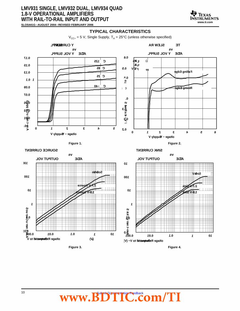
TYPICAL CHARACTERISTICS
−0.01
0.01
0.03
0.05
0.07
0.09
0.1 1
0.13
0.15
0.17
0 1 2 3 4 5
Supply V oltage − V
Supply Current − mA
SUPPL Y CURRENTvs
SUPPL Y VOL TAGE
125 °C
85 °C
25 °C
−40 °C
0.25
0.3
0.35
0.4
0.45
0.5
0.55
0.6
0 1 2 3 4 5 6
Supply V oltage − V
SLEW RA TEvs
SUPPL Y VOL TAGE
RL = 2 k ΩAV = 1VI = 1 V pp
Falling Edge
Rising Edge
Slew Rate − V/
µs
0.01
0.1
1
10
100
1000
0.001 0.01 0.1 1 10
Source Current − mA
SOURCE CURRENTvs
OUTPUT VOL TAGE
5-V Source
1.8-V Source
2.7-V Source
Output V oltage Referenced to V + (V)
SINK CURRENTvs
OUTPUT VOL TAGE
0.01
0.1
1
10
100
1000
0.001 0.01 0.1 1 10
Output V oltage Referenced to V− (V)
Sink Current − mA
5-V Sink
2.7-V Sink
1.8-V Sink
LMV931 SINGLE,, LMV932 DUAL,, LMV934 QUAD1.8-V OPERATIONAL AMPLIFIERSWITH RAIL-TO-RAIL INPUT AND OUTPUTSLOS441G–AUGUST 2004–REVISED FEBRUARY 2006
VCC+ = 5 V, Single Supply, TA = 25°C (unless otherwise specified)
Figure 1. Figure 2.
Figure 3. Figure 4.
10 Submit Documentation Feedbackwww.BDTIC.com/TI
www.ti.com
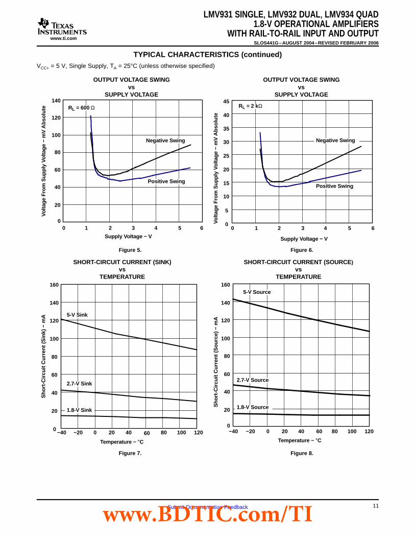
OUTPUT VOLTAGE SWINGvs
SUPPLY VOLTAGE
0
20
40
60
80
100
120
140
0 1 2 3 4 5 6
Supply Voltage − V
Vo
ltag
e F
rom
Su
pp
ly V
olta
ge
− m
V A
bso
lute RL = 600 Ω
Negative Swing
Positive Swing
0
5
10
15
20
25
30
35
40
45
0 1 2 3 4 5 6
Supply Voltage − V
OUTPUT VOLTAGE SWINGvs
SUPPLY VOLTAGE
RL = 2 kΩ
Negative Swing
Positive Swing
Vo
ltag
e F
rom
Su
pp
ly V
olta
ge
− m
V A
bso
lute
0
20
40
60
80
100
120
140
160
−40 −20 0 20 40 60 80 100 120
SHORT-CIRCUIT CURRENT (SOURCE)vs
TEMPERATURE
5-V Source
2.7-V Source
1.8-V Source
Temperature − °C
Sh
ort
-Cir
cuit
Cu
rren
t (S
ou
rce)
− m
A
SHORT-CIRCUIT CURRENT (SINK)
vsTEMPERATURE
0
20
40
60
80
100
120
140
160
−40 −20 0 20 40 60 80 100 120
5-V Sink
2.7-V Sink
1.8-V Sink
Temperature − °C
Sh
ort
-Cir
cuit
Cu
rren
t (S
ink)
− m
A
LMV931 SINGLE,, LMV932 DUAL,, LMV934 QUAD1.8-V OPERATIONAL AMPLIFIERS
WITH RAIL-TO-RAIL INPUT AND OUTPUTSLOS441G–AUGUST 2004–REVISED FEBRUARY 2006
TYPICAL CHARACTERISTICS (continued)VCC+ = 5 V, Single Supply, TA = 25°C (unless otherwise specified)
Figure 5. Figure 6.
Figure 7. Figure 8.
11Submit Documentation Feedbackwww.BDTIC.com/TI

www.ti.com
−10
0
10
20
30
40
50
60
10k 100k 1M 10M
Frequency − Hz
Gai
n −
dB
−30
−10
10
30
50
70
90
110
Ph
ase
Mar
gin
− D
eg
1.8-V FREQUENCY RESPONSEvsCL
VS = 1.8 VRL = 600 ΩPhase
Gain
CL = 0 pFCL = 300 pFCL = 1000 pF
−10
0
10
20
30
40
50
60
10k 100k 1M 10M
Frequency − Hz
Gai
n −
dB
−30
−10
10
30
50
70
90
110
Ph
ase
Mar
gin
− D
eg
5-V FREQUENCY RESPONSEvsCL
VS = 5 VRL = 600 ΩPhase
Gain
CL = 0 pFCL = 300 pFCL = 1000 pF
LMV931 SINGLE,, LMV932 DUAL,, LMV934 QUAD1.8-V OPERATIONAL AMPLIFIERSWITH RAIL-TO-RAIL INPUT AND OUTPUTSLOS441G–AUGUST 2004–REVISED FEBRUARY 2006
TYPICAL CHARACTERISTICS (continued)VCC+ = 5 V, Single Supply, TA = 25°C (unless otherwise specified)
Figure 9.
Figure 10.
12 Submit Documentation Feedbackwww.BDTIC.com/TI

www.ti.com
−10
0
10
20
30
40
50
60
10k 100k 1M 10M
Frequency − Hz
Gai
n −
dB
Ph
ase
Mar
gin
− D
eg
1.8-V FREQUENCY RESPONSEvs
TEMPERATURE
Gain
VS = 1.8 VRL = 600 ΩCL = 150 pFPhase
−30
−10
10
30
50
70
90
110
25°C
85°C
−40°C
125°C
85°C125°C
−40°C 25°C
−10
0
10
20
30
40
50
60
10k 100k 1M 10M
Frequency − Hz
Gai
n −
dB
Ph
ase
Mar
gin
− D
eg
5-V FREQUENCY RESPONSEvs
TEMPERATURE
Gain
VS = 5 VRL = 600 ΩCL = 150 pFPhase
25°C
85°C
−40°C
125°C
85°C125°C
−40°C 25°C
−30
−10
10
30
50
70
90
110
LMV931 SINGLE,, LMV932 DUAL,, LMV934 QUAD1.8-V OPERATIONAL AMPLIFIERS
WITH RAIL-TO-RAIL INPUT AND OUTPUTSLOS441G–AUGUST 2004–REVISED FEBRUARY 2006
TYPICAL CHARACTERISTICS (continued)VCC+ = 5 V, Single Supply, TA = 25°C (unless otherwise specified)
Figure 11.
Figure 12.
13Submit Documentation Feedbackwww.BDTIC.com/TI

www.ti.com
50
60
70
90
100
10 100 1k 10k 100k
Frequency − Hz
CM
RR
− d
B
CMRRvs
FREQUENCY
1.8 V2.7 V5 V
80
30
40
50
60
70
80
90
100
10 100 1k 10k
Frequency − Hz
Gai
n −
dB
PSRRvs
FREQUENCY
+PSRR
−PSRR
0.001
0.01
0.1
1
10
Frequency − Hz
TH
D −
%
THDvs
FREQUENCY
10 100 1k 10k 100k
RL = 600 ΩAV = 10
1.8 V2.7 V5 V
10 100 1k 10k 100kFrequency − Hz
TH
D −
%
0.001
0.01
0.1
1
10
THDvs
FREQUENCY
RL = 600 ΩAV = 1
1.8 V2.7 V5 V
LMV931 SINGLE,, LMV932 DUAL,, LMV934 QUAD1.8-V OPERATIONAL AMPLIFIERSWITH RAIL-TO-RAIL INPUT AND OUTPUTSLOS441G–AUGUST 2004–REVISED FEBRUARY 2006
TYPICAL CHARACTERISTICS (continued)VCC+ = 5 V, Single Supply, TA = 25°C (unless otherwise specified)
Figure 13. Figure 14.
Figure 15. Figure 16.
14 Submit Documentation Feedbackwww.BDTIC.com/TI

www.ti.com
−0.1
−0.05
0
0.05
0.1
0.15
0.2
0.25
Ou
tpu
t V
olta
ge
− V
−0.25
0
Inp
ut V
olta
ge
− V
SMALL-SIGNAL NONINVERTING RESPONSE
VS = 1.8 VRL = 2 kΩ Input
Output
−0.2
−0.15
−0.1
−0.05
0.05
0.1
0.25 µs/div
SMALL-SIGNAL NONINVERTING RESPONSE
−0.1
−0.05
0
0.05
0.1
0.15
0.2
0.25
Ou
tpu
t V
olta
ge
− V
−0.25
−0.2
−0.15
−0.1
−0.05
0
0.05
0.1 VS = 2.7 VRL = 2 kΩ Input
Output
Inp
ut V
olta
ge
− V
0.25 µs/div
0.05
SMALL-SIGNAL NONINVERTING RESPONSE
−0.1
−0.05
0
0.05
0.1
0.15
0.2
0.25
Ou
tpu
t V
olta
ge
− V
−0.25
−0.2
−0.15
−0.1
−0.05
0
0.1VS = 5 VRL = 2 kΩ Input
Output
Inp
ut V
olta
ge
− V
0.25 µs/div−1.8
−0.9
0
0.9
1.8
2.7
3.6
4.5
Ou
tpu
t V
olta
ge
− V
−4.5
−3.6
−2.7
−1.8
−0.9
0
0.9
1.8LARGE-SIGNAL NONINVERTING RESPONSE
VS = 1.8 VRL = 2 kΩAV = 1
Input
Output
Inp
ut V
olta
ge
− V
10 µs/div
LMV931 SINGLE,, LMV932 DUAL,, LMV934 QUAD1.8-V OPERATIONAL AMPLIFIERS
WITH RAIL-TO-RAIL INPUT AND OUTPUTSLOS441G–AUGUST 2004–REVISED FEBRUARY 2006
TYPICAL CHARACTERISTICS (continued)VCC+ = 5 V, Single Supply, TA = 25°C (unless otherwise specified)
Figure 17. Figure 18.
Figure 19. Figure 20.
15Submit Documentation Feedbackwww.BDTIC.com/TI

www.ti.comO
utp
ut
Vo
ltag
e −
V
Inp
ut V
olta
ge
− V
LARGE-SIGNAL NONINVERTING RESPONSE
−2.7
−1.35
0
1.35
2.7
4.05
5.4
6.75
−6.75
−5.4
−4.05
−2.7
−1.35
0
1.35
2.7VS = 2.7 VRL = 2 kΩAV = 1
Input
Output
10 µs/div−5
−2.5
0
2.5
5
7.5
10
12.5
−12.5
−10
−7.5
−5
−2.5
0
2.5
5
Ou
tpu
t V
olta
ge
− V
LARGE-SIGNAL NONINVERTING RESPONSE
VS = 5 VRL = 2 kΩAV = 1
Input
Output
Inp
ut V
olta
ge
− V
10 µs/div
−3
−2.5
−2
−1.5
−1
−0.5
0
0.5
1
−0.4 0.1 0.6 1.1 1.6 2.1 2.6 3.1
OFFSET VOLTAGEvs
COMMON-MODE RANGE
125°C85°C25°C−40°C
VIO
− m
V
VIC − V
VS = 2.7 V
OFFSET VOLTAGEvs
COMMON-MODE RANGE
−3
−2.5
−2
−1.5
−1
−0.5
0
0.5
1
−0.4 0 0.4 0.8 1.2 1.6 2 2.4
VS = 1.8 V
VIO
− m
V
VIC − V
125°C85°C25°C−40°C
LMV931 SINGLE,, LMV932 DUAL,, LMV934 QUAD1.8-V OPERATIONAL AMPLIFIERSWITH RAIL-TO-RAIL INPUT AND OUTPUTSLOS441G–AUGUST 2004–REVISED FEBRUARY 2006
TYPICAL CHARACTERISTICS (continued)VCC+ = 5 V, Single Supply, TA = 25°C (unless otherwise specified)
Figure 21. Figure 22.
Figure 23. Figure 24.
16 Submit Documentation Feedbackwww.BDTIC.com/TI

www.ti.com
−3
−2.5
−2
−1.5
−1
−0.5
0
0.5
1
−0.4 0.6 1.6 2.6 3.6 4.6 5.6
OFFSET VOLTAGEvs
COMMON-MODE RANGE
VIO
− m
V
VIC − V
VS = 5 V
125°C85°C25°C−40°C
LMV931 SINGLE,, LMV932 DUAL,, LMV934 QUAD1.8-V OPERATIONAL AMPLIFIERS
WITH RAIL-TO-RAIL INPUT AND OUTPUTSLOS441G–AUGUST 2004–REVISED FEBRUARY 2006
TYPICAL CHARACTERISTICS (continued)VCC+ = 5 V, Single Supply, TA = 25°C (unless otherwise specified)
Figure 25.
17Submit Documentation Feedbackwww.BDTIC.com/TI

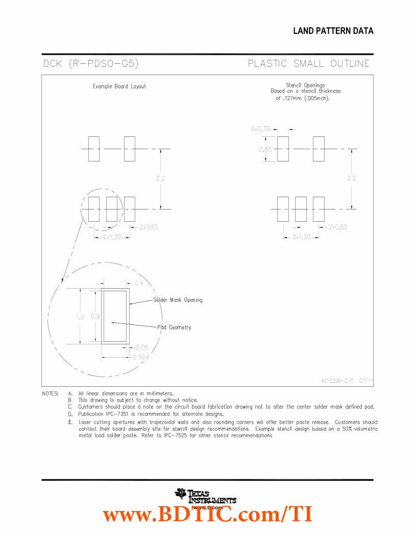
PACKAGING INFORMATION
Orderable Device Status (1) PackageType
PackageDrawing
Pins PackageQty
Eco Plan (2) Lead/Ball Finish MSL Peak Temp (3)
LMV931IDBVR ACTIVE SOT-23 DBV 5 3000 Green (RoHS &no Sb/Br)
CU NIPDAU Level-1-260C-UNLIM
LMV931IDBVRE4 ACTIVE SOT-23 DBV 5 3000 Green (RoHS &no Sb/Br)
CU NIPDAU Level-1-260C-UNLIM
LMV931IDBVRG4 ACTIVE SOT-23 DBV 5 3000 Green (RoHS &no Sb/Br)
CU NIPDAU Level-1-260C-UNLIM
LMV931IDCKR ACTIVE SC70 DCK 5 3000 Green (RoHS &no Sb/Br)
CU NIPDAU Level-1-260C-UNLIM
LMV931IDCKRE4 ACTIVE SC70 DCK 5 3000 Green (RoHS &no Sb/Br)
CU NIPDAU Level-1-260C-UNLIM
LMV931IDCKRG4 ACTIVE SC70 DCK 5 3000 Green (RoHS &no Sb/Br)
CU NIPDAU Level-1-260C-UNLIM
LMV932ID ACTIVE SOIC D 8 75 Green (RoHS &no Sb/Br)
CU NIPDAU Level-1-260C-UNLIM
LMV932IDE4 ACTIVE SOIC D 8 75 Green (RoHS &no Sb/Br)
CU NIPDAU Level-1-260C-UNLIM
LMV932IDG4 ACTIVE SOIC D 8 75 Green (RoHS &no Sb/Br)
CU NIPDAU Level-1-260C-UNLIM
LMV932IDGKR ACTIVE MSOP DGK 8 2500 Green (RoHS &no Sb/Br)
CU NIPDAU Level-1-260C-UNLIM
LMV932IDGKRG4 ACTIVE MSOP DGK 8 2500 Green (RoHS &no Sb/Br)
CU NIPDAU Level-1-260C-UNLIM
LMV932IDR ACTIVE SOIC D 8 2500 Green (RoHS &no Sb/Br)
CU NIPDAU Level-1-260C-UNLIM
LMV932IDRE4 ACTIVE SOIC D 8 2500 Green (RoHS &no Sb/Br)
CU NIPDAU Level-1-260C-UNLIM
LMV932IDRG4 ACTIVE SOIC D 8 2500 Green (RoHS &no Sb/Br)
CU NIPDAU Level-1-260C-UNLIM
LMV934ID ACTIVE SOIC D 14 50 Green (RoHS &no Sb/Br)
CU NIPDAU Level-1-260C-UNLIM
LMV934IDE4 ACTIVE SOIC D 14 50 Green (RoHS &no Sb/Br)
CU NIPDAU Level-1-260C-UNLIM
LMV934IDG4 ACTIVE SOIC D 14 50 Green (RoHS &no Sb/Br)
CU NIPDAU Level-1-260C-UNLIM
LMV934IDR ACTIVE SOIC D 14 2500 Green (RoHS &no Sb/Br)
CU NIPDAU Level-1-260C-UNLIM
LMV934IDRE4 ACTIVE SOIC D 14 2500 Green (RoHS &no Sb/Br)
CU NIPDAU Level-1-260C-UNLIM
LMV934IDRG4 ACTIVE SOIC D 14 2500 Green (RoHS &no Sb/Br)
CU NIPDAU Level-1-260C-UNLIM
LMV934IPW ACTIVE TSSOP PW 14 90 Green (RoHS &no Sb/Br)
CU NIPDAU Level-1-260C-UNLIM
LMV934IPWE4 ACTIVE TSSOP PW 14 90 Green (RoHS &no Sb/Br)
CU NIPDAU Level-1-260C-UNLIM
LMV934IPWG4 ACTIVE TSSOP PW 14 90 Green (RoHS &no Sb/Br)
CU NIPDAU Level-1-260C-UNLIM
LMV934IPWR ACTIVE TSSOP PW 14 2000 Green (RoHS &no Sb/Br)
CU NIPDAU Level-1-260C-UNLIM
LMV934IPWRE4 ACTIVE TSSOP PW 14 2000 Green (RoHS &no Sb/Br)
CU NIPDAU Level-1-260C-UNLIM
PACKAGE OPTION ADDENDUM
www.ti.com 18-Sep-2008
Addendum-Page 1
www.BDTIC.com/TI

Orderable Device Status (1) PackageType
PackageDrawing
Pins PackageQty
Eco Plan (2) Lead/Ball Finish MSL Peak Temp (3)
LMV934IPWRG4 ACTIVE TSSOP PW 14 2000 Green (RoHS &no Sb/Br)
CU NIPDAU Level-1-260C-UNLIM
(1) The marketing status values are defined as follows:ACTIVE: Product device recommended for new designs.LIFEBUY: TI has announced that the device will be discontinued, and a lifetime-buy period is in effect.NRND: Not recommended for new designs. Device is in production to support existing customers, but TI does not recommend using this part ina new design.PREVIEW: Device has been announced but is not in production. Samples may or may not be available.OBSOLETE: TI has discontinued the production of the device.
(2) Eco Plan - The planned eco-friendly classification: Pb-Free (RoHS), Pb-Free (RoHS Exempt), or Green (RoHS & no Sb/Br) - please checkhttp://www.ti.com/productcontent for the latest availability information and additional product content details.TBD: The Pb-Free/Green conversion plan has not been defined.Pb-Free (RoHS): TI's terms "Lead-Free" or "Pb-Free" mean semiconductor products that are compatible with the current RoHS requirementsfor all 6 substances, including the requirement that lead not exceed 0.1% by weight in homogeneous materials. Where designed to be solderedat high temperatures, TI Pb-Free products are suitable for use in specified lead-free processes.Pb-Free (RoHS Exempt): This component has a RoHS exemption for either 1) lead-based flip-chip solder bumps used between the die andpackage, or 2) lead-based die adhesive used between the die and leadframe. The component is otherwise considered Pb-Free (RoHScompatible) as defined above.Green (RoHS & no Sb/Br): TI defines "Green" to mean Pb-Free (RoHS compatible), and free of Bromine (Br) and Antimony (Sb) based flameretardants (Br or Sb do not exceed 0.1% by weight in homogeneous material)
(3) MSL, Peak Temp. -- The Moisture Sensitivity Level rating according to the JEDEC industry standard classifications, and peak soldertemperature.
Important Information and Disclaimer:The information provided on this page represents TI's knowledge and belief as of the date that it isprovided. TI bases its knowledge and belief on information provided by third parties, and makes no representation or warranty as to theaccuracy of such information. Efforts are underway to better integrate information from third parties. TI has taken and continues to takereasonable steps to provide representative and accurate information but may not have conducted destructive testing or chemical analysis onincoming materials and chemicals. TI and TI suppliers consider certain information to be proprietary, and thus CAS numbers and other limitedinformation may not be available for release.
In no event shall TI's liability arising out of such information exceed the total purchase price of the TI part(s) at issue in this document sold by TIto Customer on an annual basis.
OTHER QUALIFIED VERSIONS OF LMV931 :
• Automotive: LMV931-Q1
NOTE: Qualified Version Definitions:
• Automotive - Q100 devices qualified for high-reliability automotive applications targeting zero defects
PACKAGE OPTION ADDENDUM
www.ti.com 18-Sep-2008
Addendum-Page 2
www.BDTIC.com/TI

TAPE AND REEL INFORMATION
*All dimensions are nominal
Device PackageType
PackageDrawing
Pins SPQ ReelDiameter
(mm)
ReelWidth
W1 (mm)
A0(mm)
B0(mm)
K0(mm)
P1(mm)
W(mm)
Pin1Quadrant
LMV931IDBVR SOT-23 DBV 5 3000 180.0 9.2 3.17 3.23 1.37 4.0 8.0 Q3
LMV931IDBVR SOT-23 DBV 5 3000 178.0 9.0 3.23 3.17 1.37 4.0 8.0 Q3
LMV931IDCKR SC70 DCK 5 3000 180.0 9.2 2.3 2.55 1.2 4.0 8.0 Q3
LMV931IDCKR SC70 DCK 5 3000 178.0 9.0 2.4 2.5 1.2 4.0 8.0 Q3
LMV932IDGKR MSOP DGK 8 2500 330.0 12.4 5.3 3.4 1.4 8.0 12.0 Q1
LMV932IDR SOIC D 8 2500 330.0 12.4 6.4 5.2 2.1 8.0 12.0 Q1
LMV934IDR SOIC D 14 2500 330.0 16.4 6.5 9.0 2.1 8.0 16.0 Q1
LMV934IPWR TSSOP PW 14 2000 330.0 12.4 6.9 5.6 1.6 8.0 12.0 Q1
PACKAGE MATERIALS INFORMATION
www.ti.com 8-Jul-2011
Pack Materials-Page 1
www.BDTIC.com/TI

*All dimensions are nominal
Device Package Type Package Drawing Pins SPQ Length (mm) Width (mm) Height (mm)
LMV931IDBVR SOT-23 DBV 5 3000 205.0 200.0 33.0
LMV931IDBVR SOT-23 DBV 5 3000 180.0 180.0 18.0
LMV931IDCKR SC70 DCK 5 3000 205.0 200.0 33.0
LMV931IDCKR SC70 DCK 5 3000 180.0 180.0 18.0
LMV932IDGKR MSOP DGK 8 2500 358.0 335.0 35.0
LMV932IDR SOIC D 8 2500 340.5 338.1 20.6
LMV934IDR SOIC D 14 2500 346.0 346.0 33.0
LMV934IPWR TSSOP PW 14 2000 346.0 346.0 29.0
PACKAGE MATERIALS INFORMATION
www.ti.com 8-Jul-2011
Pack Materials-Page 2
www.BDTIC.com/TI

www.BDTIC.com/TI

www.BDTIC.com/TI

www.BDTIC.com/TI
www.BDTIC.com/TI

www.BDTIC.com/TI

www.BDTIC.com/TI

www.BDTIC.com/TI

www.BDTIC.com/TI

www.BDTIC.com/TI

www.BDTIC.com/TI

www.BDTIC.com/TI

IMPORTANT NOTICE
Texas Instruments Incorporated and its subsidiaries (TI) reserve the right to make corrections, modifications, enhancements, improvements,and other changes to its products and services at any time and to discontinue any product or service without notice. Customers shouldobtain the latest relevant information before placing orders and should verify that such information is current and complete. All products aresold subject to TI’s terms and conditions of sale supplied at the time of order acknowledgment.
TI warrants performance of its hardware products to the specifications applicable at the time of sale in accordance with TI’s standardwarranty. Testing and other quality control techniques are used to the extent TI deems necessary to support this warranty. Except wheremandated by government requirements, testing of all parameters of each product is not necessarily performed.
TI assumes no liability for applications assistance or customer product design. Customers are responsible for their products andapplications using TI components. To minimize the risks associated with customer products and applications, customers should provideadequate design and operating safeguards.
TI does not warrant or represent that any license, either express or implied, is granted under any TI patent right, copyright, mask work right,or other TI intellectual property right relating to any combination, machine, or process in which TI products or services are used. Informationpublished by TI regarding third-party products or services does not constitute a license from TI to use such products or services or awarranty or endorsement thereof. Use of such information may require a license from a third party under the patents or other intellectualproperty of the third party, or a license from TI under the patents or other intellectual property of TI.
Reproduction of TI information in TI data books or data sheets is permissible only if reproduction is without alteration and is accompaniedby all associated warranties, conditions, limitations, and notices. Reproduction of this information with alteration is an unfair and deceptivebusiness practice. TI is not responsible or liable for such altered documentation. Information of third parties may be subject to additionalrestrictions.
Resale of TI products or services with statements different from or beyond the parameters stated by TI for that product or service voids allexpress and any implied warranties for the associated TI product or service and is an unfair and deceptive business practice. TI is notresponsible or liable for any such statements.
TI products are not authorized for use in safety-critical applications (such as life support) where a failure of the TI product would reasonablybe expected to cause severe personal injury or death, unless officers of the parties have executed an agreement specifically governingsuch use. Buyers represent that they have all necessary expertise in the safety and regulatory ramifications of their applications, andacknowledge and agree that they are solely responsible for all legal, regulatory and safety-related requirements concerning their productsand any use of TI products in such safety-critical applications, notwithstanding any applications-related information or support that may beprovided by TI. Further, Buyers must fully indemnify TI and its representatives against any damages arising out of the use of TI products insuch safety-critical applications.
TI products are neither designed nor intended for use in military/aerospace applications or environments unless the TI products arespecifically designated by TI as military-grade or "enhanced plastic." Only products designated by TI as military-grade meet militaryspecifications. Buyers acknowledge and agree that any such use of TI products which TI has not designated as military-grade is solely atthe Buyer's risk, and that they are solely responsible for compliance with all legal and regulatory requirements in connection with such use.
TI products are neither designed nor intended for use in automotive applications or environments unless the specific TI products aredesignated by TI as compliant with ISO/TS 16949 requirements. Buyers acknowledge and agree that, if they use any non-designatedproducts in automotive applications, TI will not be responsible for any failure to meet such requirements.
Following are URLs where you can obtain information on other Texas Instruments products and application solutions:
Products Applications
Audio www.ti.com/audio Communications and Telecom www.ti.com/communications
Amplifiers amplifier.ti.com Computers and Peripherals www.ti.com/computers
Data Converters dataconverter.ti.com Consumer Electronics www.ti.com/consumer-apps
DLP® Products www.dlp.com Energy and Lighting www.ti.com/energy
DSP dsp.ti.com Industrial www.ti.com/industrial
Clocks and Timers www.ti.com/clocks Medical www.ti.com/medical
Interface interface.ti.com Security www.ti.com/security
Logic logic.ti.com Space, Avionics and Defense www.ti.com/space-avionics-defense
Power Mgmt power.ti.com Transportation and www.ti.com/automotiveAutomotive
Microcontrollers microcontroller.ti.com Video and Imaging www.ti.com/video
RFID www.ti-rfid.com Wireless www.ti.com/wireless-apps
RF/IF and ZigBee® Solutions www.ti.com/lprf
TI E2E Community Home Page e2e.ti.com
Mailing Address: Texas Instruments, Post Office Box 655303, Dallas, Texas 75265Copyright © 2011, Texas Instruments Incorporated
www.BDTIC.com/TI
Related Documents