Product Folder Sample & Buy Technical Documents Tools & Software Support & Community An IMPORTANT NOTICE at the end of this data sheet addresses availability, warranty, changes, use in safety-critical applications, intellectual property matters and other important disclaimers. PRODUCTION DATA. LM36923 SNVSA30A – MARCH 2015 – REVISED OCTOBER 2016 LM36923 Highly Efficient Triple-String White LED Driver 1 1 Features 1• 1% Matched Current Sinks Across (Process, Voltage, Temp) • 3% Current Sink Accuracy Across (Process, Voltage, Temp) • 11-Bit Dimming Resolution • Up to 91.6% Solution Efficiency • Drives from One to Three Parallel LED Strings at up to 28 V • PWM Dimming Input • I 2 C Programmable • Selectable 500-kHz and 1-MHz Switching Frequency with Optional –12% shift • Auto Switch Frequency Mode (250 kHz, 500 kHz, 1 MHz) • Four Configurable Overvoltage Protection Thresholds (17 V, 21 V, 25 V, 29 V) • Four Configurable Overcurrent Protection Thresholds (750 mA, 1000 mA, 1250 mA, 1500 mA) • Thermal Shutdown Protection 2 Applications Power Source for Smart Phone and Tablet Backlighting 3 Description The LM36923 is an ultra-compact, highly efficient, threestring white-LED driver designed for LCD display backlighting. The device can power up to 8 series LEDs at up to 25 mA per string. An adaptive current regulation method allows for different LED voltages in each string while maintaining current regulation. The LED current is adjusted via an I 2 C interface or through a logic level PWM input. The PWM duty cycle is internally sensed and mapped to an 11-bit current thus allowing for a wide range of PWM frequencies and noise-free operation. The device operates over the 2.5-V to 5.5-V input voltage range and -40°C to 85°C temperature range. Device Information (1) PART NUMBER PACKAGE BODY SIZE (MAX) LM36923 DSBGA (12) 1.755 mm × 1.355 mm (1) For all available packages, see the orderable addendum at the end of the data sheet. space space space space space space Simplified Schematic Typical String-to-String Matching vs LED Current

Welcome message from author
This document is posted to help you gain knowledge. Please leave a comment to let me know what you think about it! Share it to your friends and learn new things together.
Transcript
Product
Folder
Sample &Buy
Technical
Documents
Tools &
Software
Support &Community
An IMPORTANT NOTICE at the end of this data sheet addresses availability, warranty, changes, use in safety-critical applications,intellectual property matters and other important disclaimers. PRODUCTION DATA.
LM36923SNVSA30A –MARCH 2015–REVISED OCTOBER 2016
LM36923 Highly Efficient Triple-String White LED Driver
1
1 Features1• 1% Matched Current Sinks Across (Process,
Voltage, Temp)• 3% Current Sink Accuracy Across (Process,
Voltage, Temp)• 11-Bit Dimming Resolution• Up to 91.6% Solution Efficiency• Drives from One to Three Parallel LED Strings at
up to 28 V• PWM Dimming Input• I2C Programmable• Selectable 500-kHz and 1-MHz Switching
Frequency with Optional –12% shift• Auto Switch Frequency Mode (250 kHz, 500 kHz,
1 MHz)• Four Configurable Overvoltage Protection
Thresholds (17 V, 21 V, 25 V, 29 V)• Four Configurable Overcurrent Protection
Thresholds (750 mA, 1000 mA, 1250 mA, 1500mA)
• Thermal Shutdown Protection
2 ApplicationsPower Source for Smart Phone and TabletBacklighting
3 DescriptionThe LM36923 is an ultra-compact, highly efficient,threestring white-LED driver designed for LCD displaybacklighting. The device can power up to 8 seriesLEDs at up to 25 mA per string. An adaptive currentregulation method allows for different LED voltages ineach string while maintaining current regulation.
The LED current is adjusted via an I2C interface orthrough a logic level PWM input. The PWM duty cycleis internally sensed and mapped to an 11-bit currentthus allowing for a wide range of PWM frequenciesand noise-free operation.
The device operates over the 2.5-V to 5.5-V inputvoltage range and -40°C to 85°C temperature range.
Device Information(1)
PART NUMBER PACKAGE BODY SIZE (MAX)LM36923 DSBGA (12) 1.755 mm × 1.355 mm
(1) For all available packages, see the orderable addendum atthe end of the data sheet.
space
space
space
space
space
space
Simplified SchematicTypical String-to-String Matching vs LED Current
2
LM36923SNVSA30A –MARCH 2015–REVISED OCTOBER 2016 www.ti.com
Product Folder Links: LM36923
Submit Documentation Feedback Copyright © 2015–2016, Texas Instruments Incorporated
Table of Contents1 Features .................................................................. 12 Applications ........................................................... 13 Description ............................................................. 14 Revision History..................................................... 25 Pin Configuration and Functions ......................... 36 Specifications......................................................... 4
6.1 Absolute Maximum Ratings ..................................... 46.2 ESD Ratings.............................................................. 46.3 Recommended Operating Conditions....................... 46.4 Thermal Information ................................................. 46.5 Electrical Characteristics........................................... 56.6 I2C Timing Requirements.......................................... 66.7 Typical Characteristics .............................................. 7
7 Detailed Description ............................................ 107.1 Overview ................................................................. 107.2 Functional Block Diagram ....................................... 107.3 Feature Description................................................. 117.4 Device Functional Modes........................................ 16
7.5 Programming........................................................... 257.6 Register Maps ........................................................ 26
8 Applications and Implementation ...................... 298.1 Application Information............................................ 298.2 Typical Application .................................................. 29
9 Power Supply Recommendations ...................... 379.1 Input Supply Bypassing .......................................... 37
10 Layout................................................................... 3710.1 Layout Guidelines ................................................. 3710.2 Layout Example .................................................... 40
11 Device and Documentation Support ................. 4111.1 Device Support...................................................... 4111.2 Receiving Notification of Documentation Updates 4111.3 Community Resources.......................................... 4111.4 Trademarks ........................................................... 4111.5 Electrostatic Discharge Caution............................ 4111.6 Glossary ................................................................ 41
12 Mechanical, Packaging, and OrderableInformation ........................................................... 41
4 Revision History
Changes from Original (March 2015) to Revision A Page
• Changed pin name "VOUT" to "OUT" .................................................................................................................................... 3• Changed pin name in Layout Example from 'VOUT' to 'OUT' ............................................................................................. 39
LED1 ASEL
LED2 SDA
GND
SW
LED3 SCL OUT
PWM HWEN IN
A
B
C
D
1 2 3
3
LM36923www.ti.com SNVSA30A –MARCH 2015–REVISED OCTOBER 2016
Product Folder Links: LM36923
Submit Documentation FeedbackCopyright © 2015–2016, Texas Instruments Incorporated
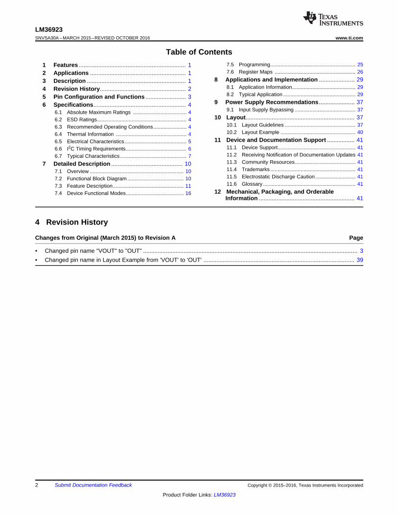
5 Pin Configuration and Functions
YFF Package12-Pin DSBGA
Top View
Pin FunctionsPIN
I/O DESCRIPTIONNUMBER NAME
A1 LED1 Input Input to current sink 1. The boost converter regulates the minimum voltage betweenLED1, LED2, LED3 to VHR.
A2 BL_ADJ Input LED current adjust input. When BL_ADJ is driven to a logic high voltage the LED currentsteps down to the programmed low current value.
A3 GND Input Ground
B1 LED2 Input Input pin to current sink 2. The boost converter regulates the minimum voltage betweenLED1, LED2 ,LED3 to VHR.
B2 SDA I/O Data I/O for I2C-Compatible Interface.
B3 SW Output Drain Connection for internal low side NFET, and anode connection for external Schottkydiode.
C1 LED3 Input Input pin to current sink 3. The boost converter regulates the minimum voltage betweenLED1, LED2, LED3 to VHR.
C2 SCL Input Clock Input for I2C-compatible interface.
C3 OUT Input OUT serves as the sense point for overvoltage protection. Connect OUT to the positivepin of the output capacitor.
D1 PWM Input Logic level input for PWM current control.
D2 HWEN Input Hardware enable input. Drive HWEN high to bring the device out of shutdown and allowI2C writes or PWM control.
D3 IN Input Input voltage connection. Bypass IN to GND with a minimum 2.2-µF ceramic capacitor.
4
LM36923SNVSA30A –MARCH 2015–REVISED OCTOBER 2016 www.ti.com
Product Folder Links: LM36923
Submit Documentation Feedback Copyright © 2015–2016, Texas Instruments Incorporated
(1) Stresses beyond those listed under absolute maximum ratings may cause permanent damage to the device. These are stress ratingsonly, and functional operation of the device at these or any other conditions beyond those indicated under recommended operatingconditions is not implied. Exposure to absolute–maximum–rated conditions for extended periods may affect device reliability.
6 Specifications
6.1 Absolute Maximum Ratingsover operating free-air temperature range (unless otherwise noted) (1)
MIN MAX UNITIN Input voltage –0.3 6 VOUT Output overvoltage sense input –0.3 30 VSW Inductor connection –0.3 30 VLED1, LED2, LED3 LED string cathode connection –0.3 30 VHWEN, PWM, SDA,SCL, BL_ADJ Logic I/Os –0.3 6 V
Maximum junction temperature, TJ_MAX 150 °CStorage temperature, Tstg –65 150 °C
(1) JEDEC document JEP155 states that 500-V HBM allows safe manufacturing with a standard ESD control process. Pins listed as ±2000V may actually have higher performance.
(2) JEDEC document JEP157 states that 250-V CDM allows safe manufacturing with a standard ESD control process. Pins listed as ±500 Vmay actually have higher performance.
6.2 ESD RatingsVALUE UNIT
V(ESD)Electrostaticdischarge
Human-body model (HBM), per ANSI/ESDA/JEDEC JS-001 (1) ±2000V
Charged-device model (CDM), per JEDEC specification JESD22-C101 (2) ±500
6.3 Recommended Operating Conditionsover operating free-air temperature range (unless otherwise noted)
MIN MAX UNITIN Input voltage 2.5 5.5 VOUT Overvoltage sense input 0 29.5 VSW Inductor connection 0 29.5 VLED1, LED2, LED3 LED string cathode connection 0 29.5 VHWEN, PWM, SDA,SCL, BL_ADJ Logic I/Os 0 5.5 V
(1) For more information about traditional and new thermal metrics, see the Semiconductor and IC Package Thermal Metrics.
6.4 Thermal Information
THERMAL METRIC (1) YFQ (DSBGA)UNIT
12 PINSRθJA Junction-to-ambient thermal resistance 88.9
°C/WRθJC(top) Junction-to-case (top) thermal resistance 0.7RθJB Junction-to-board thermal resistance 43.9ΨθJT Junction-to-top characterization parameter 2.9ΨθJB Junction-to-board characterization parameter 43.7
5
LM36923www.ti.com SNVSA30A –MARCH 2015–REVISED OCTOBER 2016
Product Folder Links: LM36923
Submit Documentation FeedbackCopyright © 2015–2016, Texas Instruments Incorporated
(1) LED Current Matching between strings is given as the worst case matching between any two strings. Matching is calculated as ((ILEDX –ILEDY)/(ILEDX + ILEDY) × 100.
6.5 Electrical CharacteristicsLimits apply over the full operating ambient temperature range (−40°C ≤ TA ≤ 85°C) and VIN = 3.6 V, typical values are at TA =25°C (unless otherwise noted).
PARAMETER TEST CONDITIONS MIN TYP MAX UNITBOOSTIMATCH
(1) LED current matching ILED1 toILED2 to ILED3
50 µA ≤ ILED ≤ 25 mA, 2.7 V ≤ VIN ≤ 5 V(linear or exponential mode)
–1% 0.1% 1%
Accuracy Absolute Accuracy (ILED1,ILED2, ILED3)
50 µA ≤ ILED ≤ 25 mA, 2.7 V ≤ VIN ≤ 5 V(linear or exponential mode) –3% 0.1% 3%
ILED_MIN Minimum LED current (perstring) PWM or I2C current control (linear or
exponential mode)
50 µA
ILED_MAX Maximum LED current (perstring)
25 mA
RDNL IDAC ratio-metric DNL exponential mode only 1/3(0.3%) LSB
VHRRegulated current sinkheadroom voltage
ILED = 25 mA 210mV
ILED = 5 mA 100
VHR_MINCurrent sink minimumheadroom voltage
ILED = 95% of nominal, ILED = 5 mA 35 50 mV
Efficiency Typical efficiency VIN = 3.7 V, ILED = 5 mA/string, TypicalApplication circuit (3x7 LEDs), (POUT/PIN) 87%
RNMOS NMOS switch on resistance ISW = 250 mA 0.25 Ω
ICL NMOS switch current limit 2.7 V ≤ VIN ≤ 5 V
OCP = 00 575 750 875
mAOCP = 01 860 1000 1110OCP = 10 1100 1250 1400OCP = 11 1350 1500 1650
VOVP Output overvoltage protection ON threshold, 2.7 V ≤ VIN≤ 5 V
OVP = 00 16 17 17.5
VOVP = 01 20 21 21.5OVP = 10 24 25 25.5OVP = 11 28 29 29.5
OVPHysteresis
0.5 V
ƒSW Switching frequency2.7 V ≤ VIN ≤ 5 V, boostfrequencyshift = 0
Boost frequencyselect = 0 475 500 525
kHzBoost frequencyselect = 1
950 1000 1050
DMAX Maximum boost duty cycle 92% 94%
ISHDN Shutdown current Chip enable bit = 0, SDA = SCL = IN or GND,2.7 V ≤ VIN ≤ 5 V
1.2 5 µA
TSDThermal shutdown 135
°CHysteresis 15
PWM INPUTMin ƒPWM 50 HzMax ƒPWM Sample rate = 24 MHz 50 kHz
tMIN_ON Minimum pulse ON timeSample rate = 24 MHz 183.3
nsSample rate = 4 MHz 1100Sample rate = 800 kHz 5500
tMIN_OFF Minimum pulse OFF timeSample rate = 24 MHz 183.3
nsSample rate = 4 MHz 1100Sample rate = 800 kHz 5500
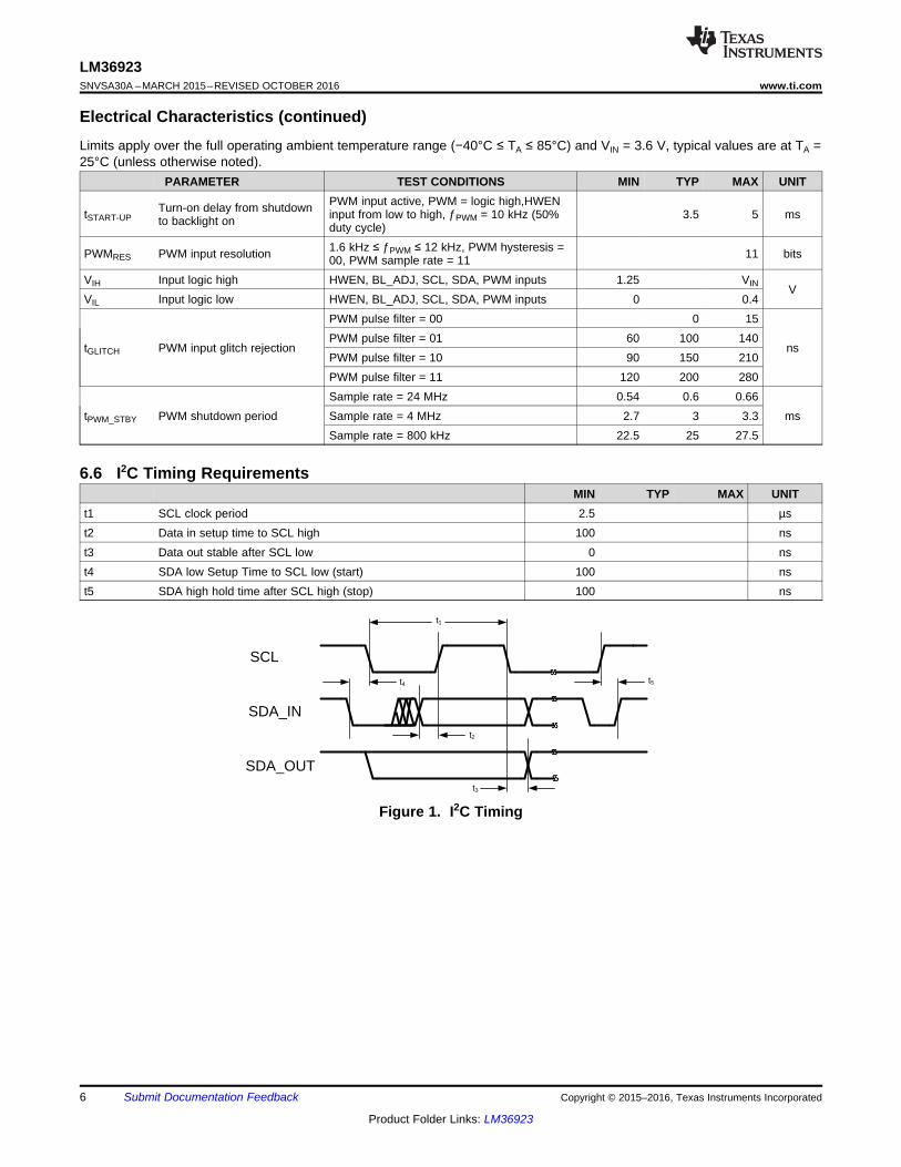
t4
t2
t3
t5
t1
SCL
SDA_IN
SDA_OUT
6
LM36923SNVSA30A –MARCH 2015–REVISED OCTOBER 2016 www.ti.com
Product Folder Links: LM36923
Submit Documentation Feedback Copyright © 2015–2016, Texas Instruments Incorporated
Electrical Characteristics (continued)Limits apply over the full operating ambient temperature range (−40°C ≤ TA ≤ 85°C) and VIN = 3.6 V, typical values are at TA =25°C (unless otherwise noted).
PARAMETER TEST CONDITIONS MIN TYP MAX UNIT
tSTART-UPTurn-on delay from shutdownto backlight on
PWM input active, PWM = logic high,HWENinput from low to high, ƒPWM = 10 kHz (50%duty cycle)
3.5 5 ms
PWMRES PWM input resolution 1.6 kHz ≤ ƒPWM ≤ 12 kHz, PWM hysteresis =00, PWM sample rate = 11 11 bits
VIH Input logic high HWEN, BL_ADJ, SCL, SDA, PWM inputs 1.25 VIN VVIL Input logic low HWEN, BL_ADJ, SCL, SDA, PWM inputs 0 0.4
tGLITCH PWM input glitch rejection
PWM pulse filter = 00 0 15
nsPWM pulse filter = 01 60 100 140PWM pulse filter = 10 90 150 210PWM pulse filter = 11 120 200 280
tPWM_STBY PWM shutdown periodSample rate = 24 MHz 0.54 0.6 0.66
msSample rate = 4 MHz 2.7 3 3.3Sample rate = 800 kHz 22.5 25 27.5
6.6 I2C Timing RequirementsMIN TYP MAX UNIT
t1 SCL clock period 2.5 µst2 Data in setup time to SCL high 100 nst3 Data out stable after SCL low 0 nst4 SDA low Setup Time to SCL low (start) 100 nst5 SDA high hold time after SCL high (stop) 100 ns
Figure 1. I2C Timing
28.1
28.2
28.3
28.4
28.5
28.6
28.7
28.8
28.9
29.0
29.1
2.50
2.75
3.00
3.25
3.50
3.75
4.00
4.25
4.50
4.75
5.00
5.25
5.50
OV
P T
HR
ES
HO
LD (
V)
VIN (V)
MAX -40 degC MIN -40 degC
MAX 30 degC MIN 30 degC
MAX 125 degC MIN 125 degC
C001
0
0.05
0.1
0.15
0.2
0.25
0.3
0.35
0.4
0.45
0.5
2.50
2.75
3.00
3.25
3.50
3.75
4.00
4.25
4.50
4.75
5.00
5.25
5.50
RD
SO
N (
Ohm
s)
VIN (V)
125 degC
30 degC
-40 degC
C001
24.1
24.2
24.3
24.4
24.5
24.6
24.7
24.8
24.9
25.0
25.1
2.50
2.75
3.00
3.25
3.50
3.75
4.00
4.25
4.50
4.75
5.00
5.25
5.50
OV
P T
HR
ES
HO
LD (
V)
VIN (V)
MAX -40 degC MIN -40 degC
MAX 30 degC MIN 30 degC
MAX 125 degC MIN 125 degC
C001
20.2
20.3
20.4
20.5
20.6
20.7
20.8
20.9
21.0
21.1
21.2
2.50
2.75
3.00
3.25
3.50
3.75
4.00
4.25
4.50
4.75
5.00
5.25
5.50
OV
P T
HR
ES
HO
LD (
V)
VIN (V)
MAX -40 degC MIN -40 degC
MAX 30 degC MIN 30 degC
MAX 125 degC MIN 125 degC
C001
0.515
0.52
0.525
0.53
0.535
0.54
2.50
2.75
3.00
3.25
3.50
3.75
4.00
4.25
4.50
4.75
5.00
5.25
5.50
OV
P H
YS
TE
RE
SIS
(V
)
VIN (V)
-40 degC
30 degC
125 degC
C001
16.2
16.3
16.4
16.5
16.6
16.7
16.8
16.9
17.0
17.1
17.2
2.50
2.75
3.00
3.25
3.50
3.75
4.00
4.25
4.50
4.75
5.00
5.25
5.50
OV
P T
HR
ES
HO
LD (
V)
VIN (V)
MAX -40 degC MIN -40 degC
MAX 30 degC MIN 30 degC
MAX 125 degC MIN 125 degC
C001
7
LM36923www.ti.com SNVSA30A –MARCH 2015–REVISED OCTOBER 2016
Product Folder Links: LM36923
Submit Documentation FeedbackCopyright © 2015–2016, Texas Instruments Incorporated
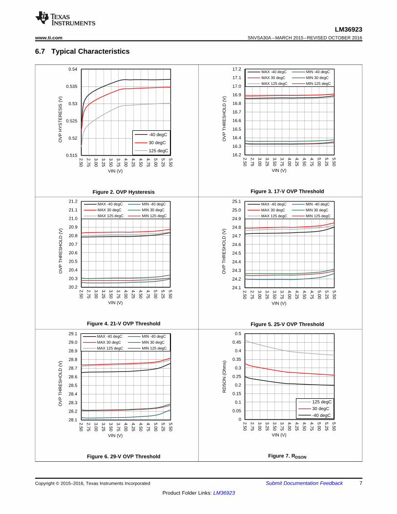
6.7 Typical Characteristics
Figure 2. OVP Hysteresis Figure 3. 17-V OVP Threshold
Figure 4. 21-V OVP Threshold Figure 5. 25-V OVP Threshold
Figure 6. 29-V OVP Threshold Figure 7. RDSON
0.96
0.97
0.98
0.99
1.00
1.01
1.02
1.03
2.50
2.75
3.00
3.25
3.50
3.75
4.00
4.25
4.50
4.75
5.00
5.25
5.50
PE
AK
CU
RR
EN
T (
A)
VIN (V)
-40 degC30 degC125 degC
C001
1.20
1.21
1.22
1.23
1.24
1.25
1.26
1.27
1.28
1.29
1.30
2.50
2.75
3.00
3.25
3.50
3.75
4.00
4.25
4.50
4.75
5.00
5.25
5.50
PE
AK
CU
RR
EN
T (
A)
VIN (V)
-40 degC30 degC125 degC
C001
200
202
204
206
208
210
212
214
216
2.50
2.75
3.00
3.25
3.50
3.75
4.00
4.25
4.50
4.75
5.00
5.25
5.50
VH
R_M
IN
(mV
)
VIN (V)
125 degC30 degC-40 degC
C001
0.70
0.71
0.72
0.73
0.74
0.75
0.76
0.77
0.78
2.50
2.75
3.00
3.25
3.50
3.75
4.00
4.25
4.50
4.75
5.00
5.25
5.50
PE
AK
CU
RR
EN
T (
A)
VIN (V)
-40 degC
30 degC
125 degC
C001
0
0.5
1
1.5
2
2.5
3
2.50
2.75
3.00
3.25
3.50
3.75
4.00
4.25
4.50
4.75
5.00
5.25
5.50
ISH
DN
(uA
)
VIN (V)
-40 degC30 degC125 degC
C001
0
0.5
1
1.5
2
2.5
2.50
2.75
3.00
3.25
3.50
3.75
4.00
4.25
4.50
4.75
5.00
5.25
5.50
SW
ITC
HIN
G IQ
(m
A)
VIN (V)
-40 degC30 degC125 degC
C001
8
LM36923SNVSA30A –MARCH 2015–REVISED OCTOBER 2016 www.ti.com
Product Folder Links: LM36923
Submit Documentation Feedback Copyright © 2015–2016, Texas Instruments Incorporated
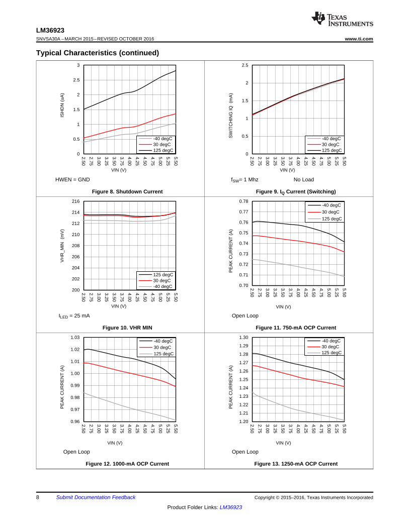
Typical Characteristics (continued)
HWEN = GND
Figure 8. Shutdown Current
fSW= 1 Mhz No Load
Figure 9. IQ Current (Switching)
ILED = 25 mA
Figure 10. VHR MIN
Open Loop
Figure 11. 750-mA OCP Current
Open Loop
Figure 12. 1000-mA OCP Current
Open Loop
Figure 13. 1250-mA OCP Current
1.43
1.44
1.45
1.46
1.47
1.48
1.49
1.50
1.51
1.52
1.53
1.54
1.55
2.50
2.75
3.00
3.25
3.50
3.75
4.00
4.25
4.50
4.75
5.00
5.25
5.50P
EA
K C
UR
RE
NT
(A
)
VIN (V)
-40 degC
30 degC
125 degC
C001
9
LM36923www.ti.com SNVSA30A –MARCH 2015–REVISED OCTOBER 2016
Product Folder Links: LM36923
Submit Documentation FeedbackCopyright © 2015–2016, Texas Instruments Incorporated
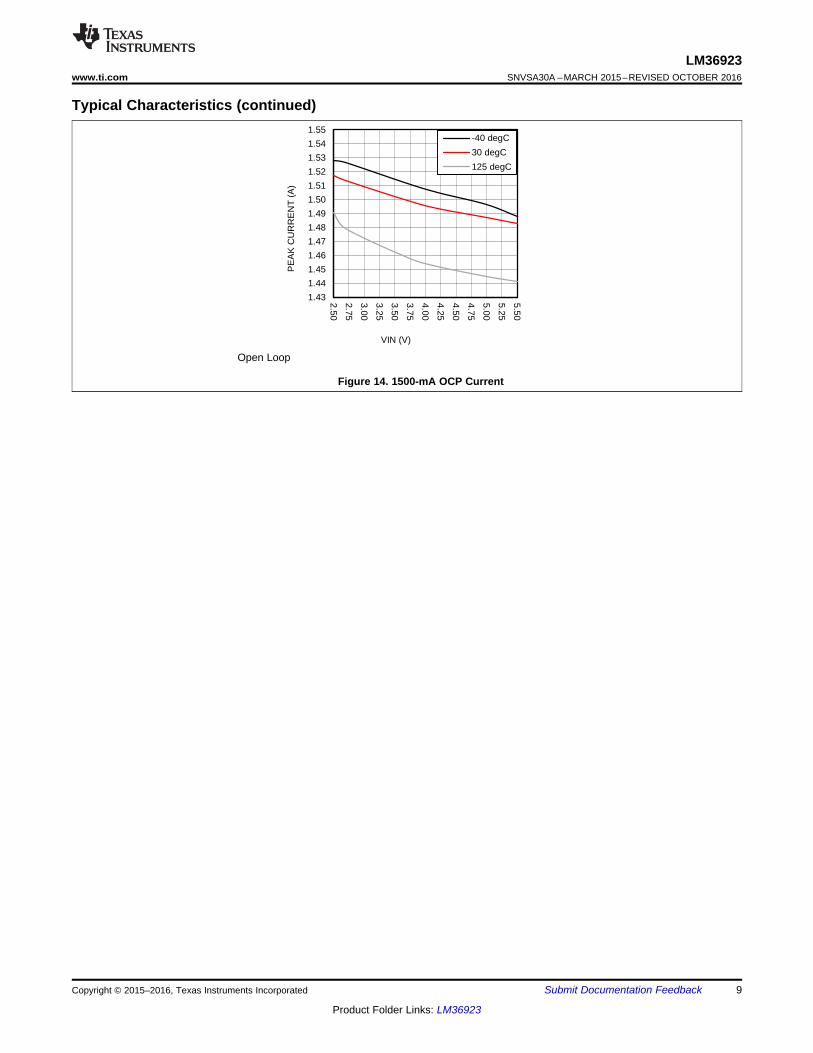
Typical Characteristics (continued)
Open Loop
Figure 14. 1500-mA OCP Current
Current Sinks
Boost Control
Overvoltage Protection
17 V21 V25 V29 V
PWM Sample Rate
800 kHz 4 MHz24 MHz
PWM Sampler
I2C Interface
Boost Switching Frequency
1 MHz887 kHz500 kHz443 kHz250 kHz220 kHz
LED Current Mapping
ExponentialLinear
LED Current RampingNo ramp
0.125 ms/step0.25 ms/step0.5 ms/step1 ms/step2 ms/step4 ms/step8 ms/step16 ms/step
Min Headroom Select
Adaptive Headroom
Fault DetectionOvervoltage
LED String ShortLED String Open
Current LimitThermal
Shutdown
Thermal Shutdown
135oC
0.25 W
Auto Frequency
Mode
Boost Current Limit
750 mA1500 mA
11-Bit Brightness
Code
LED String Enables
SW
OUT
LED1
LED2
LED3
PWM
SCL
SDA
IN
HWEN
GND
BL_ADJ Force Low Current Target
OCPLED Fault
TSD
OVP
10
LM36923SNVSA30A –MARCH 2015–REVISED OCTOBER 2016 www.ti.com
Product Folder Links: LM36923
Submit Documentation Feedback Copyright © 2015–2016, Texas Instruments Incorporated
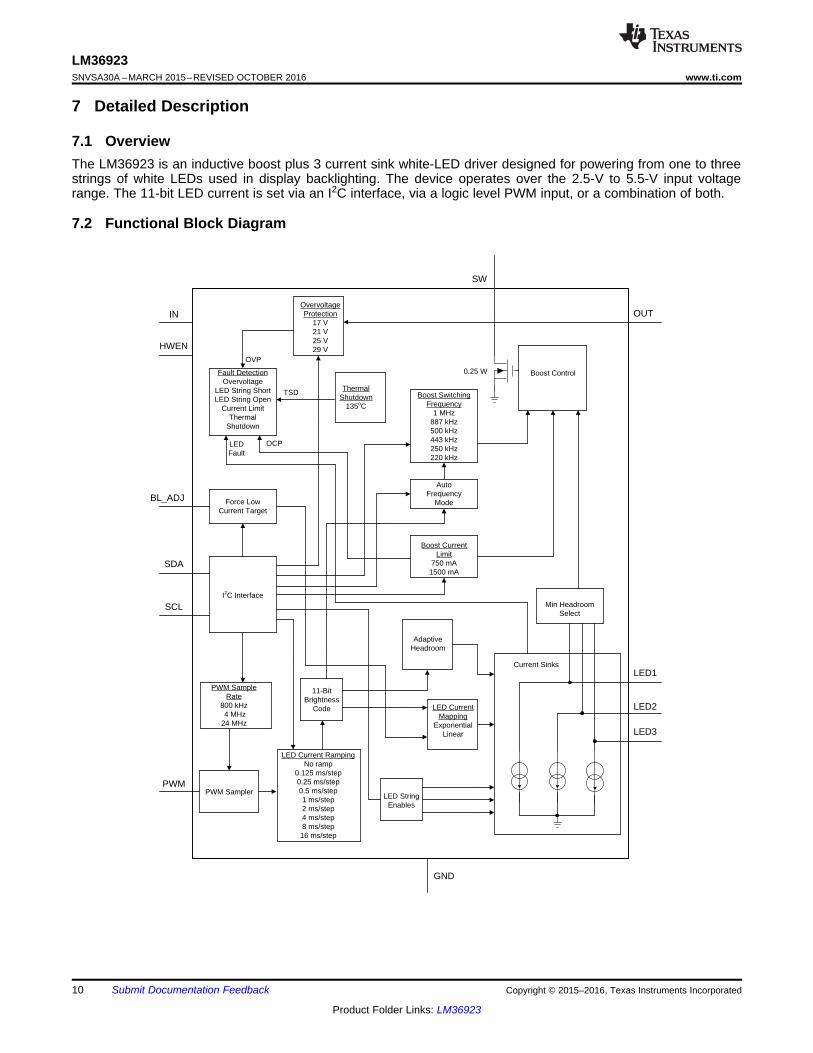
7 Detailed Description
7.1 OverviewThe LM36923 is an inductive boost plus 3 current sink white-LED driver designed for powering from one to threestrings of white LEDs used in display backlighting. The device operates over the 2.5-V to 5.5-V input voltagerange. The 11-bit LED current is set via an I2C interface, via a logic level PWM input, or a combination of both.
7.2 Functional Block Diagram
HWEN
I2C
ILED
VIN
tHWEN_I2C
I2C Registers In Reset
I2C Data ValidI2C Brightness
Data Sent
tBRT_DAC tDAC_LED
PWM
HWEN
ILED
VIN
tHWEN_PWM tPWM_DAC tDAC_LED tDD_LED tPWM_STBY
11
LM36923www.ti.com SNVSA30A –MARCH 2015–REVISED OCTOBER 2016
Product Folder Links: LM36923
Submit Documentation FeedbackCopyright © 2015–2016, Texas Instruments Incorporated
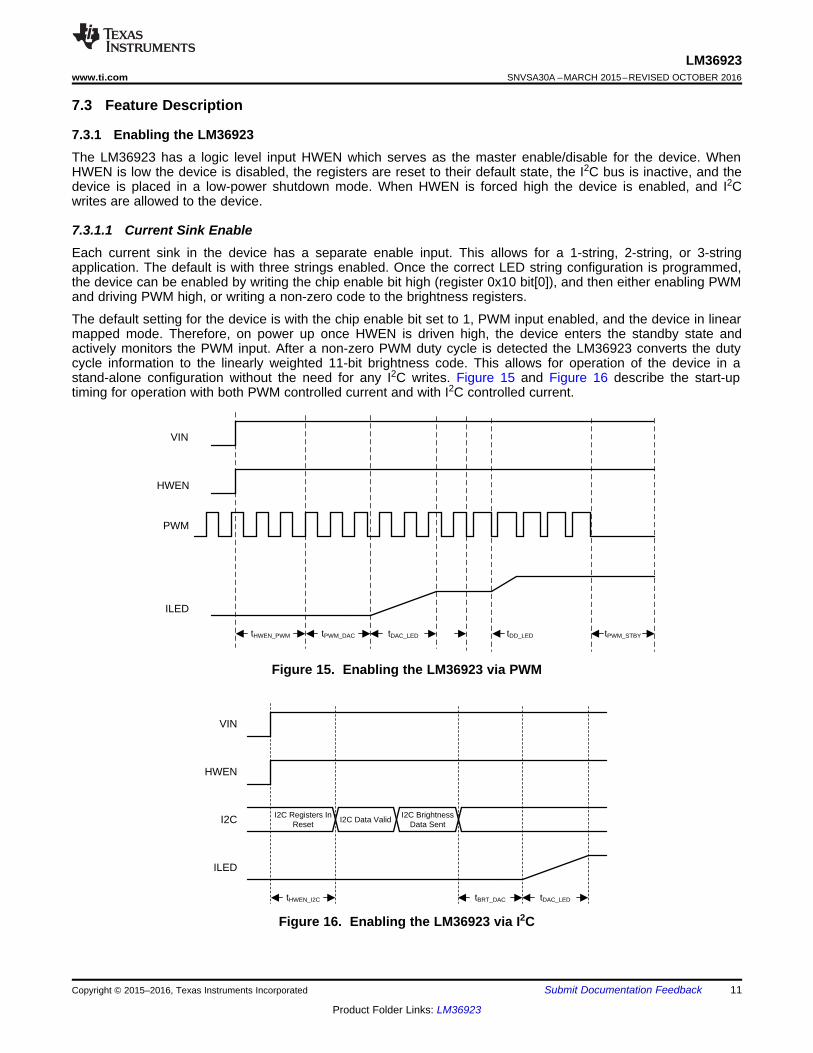
7.3 Feature Description
7.3.1 Enabling the LM36923The LM36923 has a logic level input HWEN which serves as the master enable/disable for the device. WhenHWEN is low the device is disabled, the registers are reset to their default state, the I2C bus is inactive, and thedevice is placed in a low-power shutdown mode. When HWEN is forced high the device is enabled, and I2Cwrites are allowed to the device.
7.3.1.1 Current Sink EnableEach current sink in the device has a separate enable input. This allows for a 1-string, 2-string, or 3-stringapplication. The default is with three strings enabled. Once the correct LED string configuration is programmed,the device can be enabled by writing the chip enable bit high (register 0x10 bit[0]), and then either enabling PWMand driving PWM high, or writing a non-zero code to the brightness registers.
The default setting for the device is with the chip enable bit set to 1, PWM input enabled, and the device in linearmapped mode. Therefore, on power up once HWEN is driven high, the device enters the standby state andactively monitors the PWM input. After a non-zero PWM duty cycle is detected the LM36923 converts the dutycycle information to the linearly weighted 11-bit brightness code. This allows for operation of the device in astand-alone configuration without the need for any I2C writes. Figure 15 and Figure 16 describe the start-uptiming for operation with both PWM controlled current and with I2C controlled current.
Figure 15. Enabling the LM36923 via PWM
Figure 16. Enabling the LM36923 via I2C

+.'& = 50J#× 1.003040572%K@A
+.'& = 37.806ä# +12.195ä#×%K@A
+.'& = 50J#× 1.003040572%K@A +.'& = 37.806ä# +12.195ä#×%K@A
+.'& = 50J#× 1.003040572%K@A +.'& = 37.806ä# +12.195ä#×%K@A
+.'& = 50J#× 1.003040572%K@A +.'& = 37.806ä# +12.195ä#×%K@A
12
LM36923SNVSA30A –MARCH 2015–REVISED OCTOBER 2016 www.ti.com
Product Folder Links: LM36923
Submit Documentation Feedback Copyright © 2015–2016, Texas Instruments Incorporated
Feature Description (continued)
(1) Code is the 11-bit code output from the ramper (see Figure 21, Figure 23, Figure 25, Figure 27). This can be the I2C brightness code,the converted PWM duty cycle or the 11-bit product of both.
7.3.2 LM36923 Start-UpThe LM36923 can be enabled or disabled in various ways. When disabled, the device is considered shutdown,and the quiescent current drops to ISHDN. When the device is in standby, it returns to the ISHDN current levelretaining all programmed register values. Table 1 describes the different operating states for the LM36923.
Table 1. LM36923 Operating Modes
LED STRINGENABLES
0x10 bits[3:1]PWM INPUT
I2CBRIGHTNESSREGISTERS
0x18 bits[2:0]0x19 bits[7:0]
BRIGHTNESSMODE
0x11 bits[6:5]
DEVICEENABLE
0x10 bit[0]
LED CURRENT
(EXP MAPPING)0x11 bit[7] = 1
(LIN MAPPING)0x11 bit[7] = 0
XXX X XXX XX 0 Off, device disabled0 X XXX XX 1 Off, device standby
At least oneenabled
X 0 00 1 Off, device in standby
At least oneenabled
X Code > 000 00 1See (1) See (1)
At least oneenabled
0 XXX 01 1 Off, device in standby
At least oneenabled
PWM Signal XXX 01 1See (1) See (1)
At least oneenabled
0 XXX 10 or 11 1 Off, device in standby
At least oneenabled
X 0 10 or 11 1 Off, device in standby
At least oneenabled
PWM Signal Code > 000 10 or 11 1See (1) See (1)
7.3.3 Brightness MappingThere are two different ways to map the brightness code (or PWM duty cycle) to the LED current: linear andexponential mapping.
7.3.3.1 Linear MappingFor linear mapped mode the LED current increases proportionally to the 11-bit brightness code and follows therelationship:
(1)
This is valid from codes 1 to 2047. Code 0 programs 0 current. Code is an 11-bit code that can be the I2Cbrightness code, the digitized PWM duty cycle, or the product of the two.
7.3.3.2 Exponential MappingIn exponential mapped mode the LED current follows the relationship:
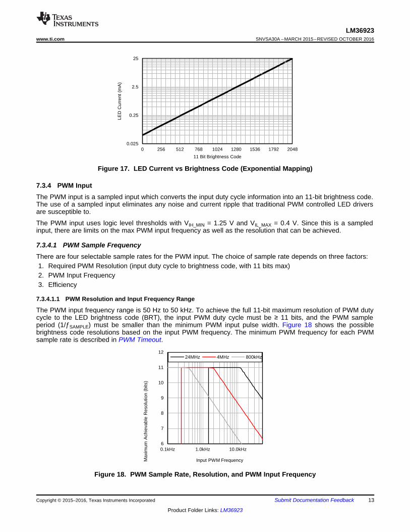
(2)
This results in an LED current step size of approximately 0.304% per code. This is valid for codes from 1 to2047. Code 0 programs 0 current. Code is an 11-bit code that can be the I2C brightness code, the digitized PWMduty cycle, or the product of the two. Figure 17 details the LED current exponential response.
The 11-bit (0.304%) per code step is small enough such that the transition from one code to the next in terms ofLED brightness is not distinguishable to the eye. This therefore gives a perfectly smooth brightness increasebetween adjacent codes.
6
7
8
9
10
11
12
0.1kHz 1.0kHz 10.0kHz
Max
imum
Ach
ieva
ble
Res
olut
ion
(bits
)
Input PWM Frequency
24MHz 4MHz 800kHz
C001
0.025
0.25
2.5
25
0 256 512 768 1024 1280 1536 1792 2048
LED
Cur
rent
(m
A)
11 Bit Brightness Code C006
13
LM36923www.ti.com SNVSA30A –MARCH 2015–REVISED OCTOBER 2016
Product Folder Links: LM36923
Submit Documentation FeedbackCopyright © 2015–2016, Texas Instruments Incorporated
Figure 17. LED Current vs Brightness Code (Exponential Mapping)
7.3.4 PWM InputThe PWM input is a sampled input which converts the input duty cycle information into an 11-bit brightness code.The use of a sampled input eliminates any noise and current ripple that traditional PWM controlled LED driversare susceptible to.
The PWM input uses logic level thresholds with VIH_MIN = 1.25 V and VIL_MAX = 0.4 V. Since this is a sampledinput, there are limits on the max PWM input frequency as well as the resolution that can be achieved.
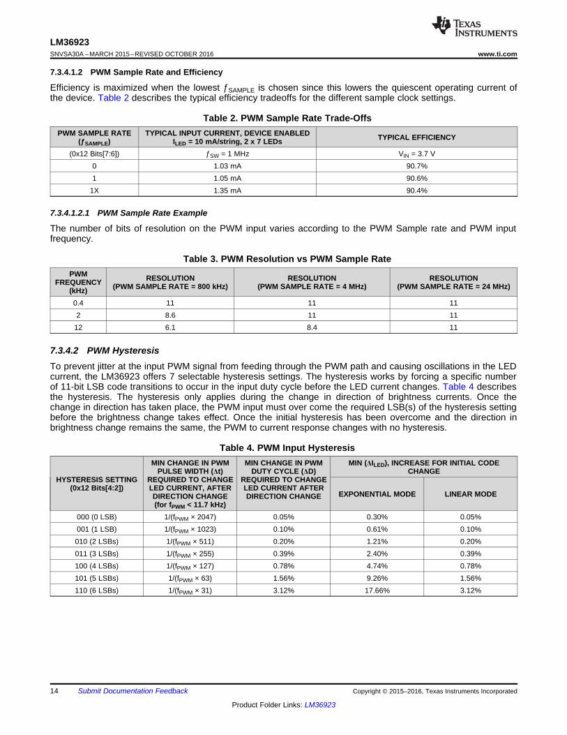
7.3.4.1 PWM Sample FrequencyThere are four selectable sample rates for the PWM input. The choice of sample rate depends on three factors:1. Required PWM Resolution (input duty cycle to brightness code, with 11 bits max)2. PWM Input Frequency3. Efficiency
7.3.4.1.1 PWM Resolution and Input Frequency Range
The PWM input frequency range is 50 Hz to 50 kHz. To achieve the full 11-bit maximum resolution of PWM dutycycle to the LED brightness code (BRT), the input PWM duty cycle must be ≥ 11 bits, and the PWM sampleperiod (1/ƒSAMPLE) must be smaller than the minimum PWM input pulse width. Figure 18 shows the possiblebrightness code resolutions based on the input PWM frequency. The minimum PWM frequency for each PWMsample rate is described in PWM Timeout.
Figure 18. PWM Sample Rate, Resolution, and PWM Input Frequency
14
LM36923SNVSA30A –MARCH 2015–REVISED OCTOBER 2016 www.ti.com
Product Folder Links: LM36923
Submit Documentation Feedback Copyright © 2015–2016, Texas Instruments Incorporated
7.3.4.1.2 PWM Sample Rate and Efficiency
Efficiency is maximized when the lowest ƒSAMPLE is chosen since this lowers the quiescent operating current ofthe device. Table 2 describes the typical efficiency tradeoffs for the different sample clock settings.
Table 2. PWM Sample Rate Trade-OffsPWM SAMPLE RATE
(ƒSAMPLE)TYPICAL INPUT CURRENT, DEVICE ENABLED
ILED = 10 mA/string, 2 x 7 LEDs TYPICAL EFFICIENCY
(0x12 Bits[7:6]) ƒSW = 1 MHz VIN = 3.7 V0 1.03 mA 90.7%1 1.05 mA 90.6%
1X 1.35 mA 90.4%
7.3.4.1.2.1 PWM Sample Rate Example
The number of bits of resolution on the PWM input varies according to the PWM Sample rate and PWM inputfrequency.
Table 3. PWM Resolution vs PWM Sample RatePWM
FREQUENCY(kHz)
RESOLUTION(PWM SAMPLE RATE = 800 kHz)
RESOLUTION(PWM SAMPLE RATE = 4 MHz)
RESOLUTION(PWM SAMPLE RATE = 24 MHz)
0.4 11 11 112 8.6 11 11
12 6.1 8.4 11
7.3.4.2 PWM HysteresisTo prevent jitter at the input PWM signal from feeding through the PWM path and causing oscillations in the LEDcurrent, the LM36923 offers 7 selectable hysteresis settings. The hysteresis works by forcing a specific numberof 11-bit LSB code transitions to occur in the input duty cycle before the LED current changes. Table 4 describesthe hysteresis. The hysteresis only applies during the change in direction of brightness currents. Once thechange in direction has taken place, the PWM input must over come the required LSB(s) of the hysteresis settingbefore the brightness change takes effect. Once the initial hysteresis has been overcome and the direction inbrightness change remains the same, the PWM to current response changes with no hysteresis.
Table 4. PWM Input Hysteresis
HYSTERESIS SETTING(0x12 Bits[4:2])
MIN CHANGE IN PWMPULSE WIDTH (Δt)
REQUIRED TO CHANGELED CURRENT, AFTERDIRECTION CHANGE(for fPWM < 11.7 kHz)
MIN CHANGE IN PWMDUTY CYCLE (ΔD)
REQUIRED TO CHANGELED CURRENT AFTERDIRECTION CHANGE
MIN (ΔILED), INCREASE FOR INITIAL CODECHANGE
EXPONENTIAL MODE LINEAR MODE
000 (0 LSB) 1/(fPWM × 2047) 0.05% 0.30% 0.05%001 (1 LSB) 1/(fPWM × 1023) 0.10% 0.61% 0.10%010 (2 LSBs) 1/(fPWM × 511) 0.20% 1.21% 0.20%011 (3 LSBs) 1/(fPWM × 255) 0.39% 2.40% 0.39%100 (4 LSBs) 1/(fPWM × 127) 0.78% 4.74% 0.78%101 (5 LSBs) 1/(fPWM × 63) 1.56% 9.26% 1.56%110 (6 LSBs) 1/(fPWM × 31) 3.12% 17.66% 3.12%
¿P =1IO
OPAL× :0T7(( F 0T444F 1; = 954IO
¿P= 4=IL_N=PA×:%K@A $F%K@A#F1;
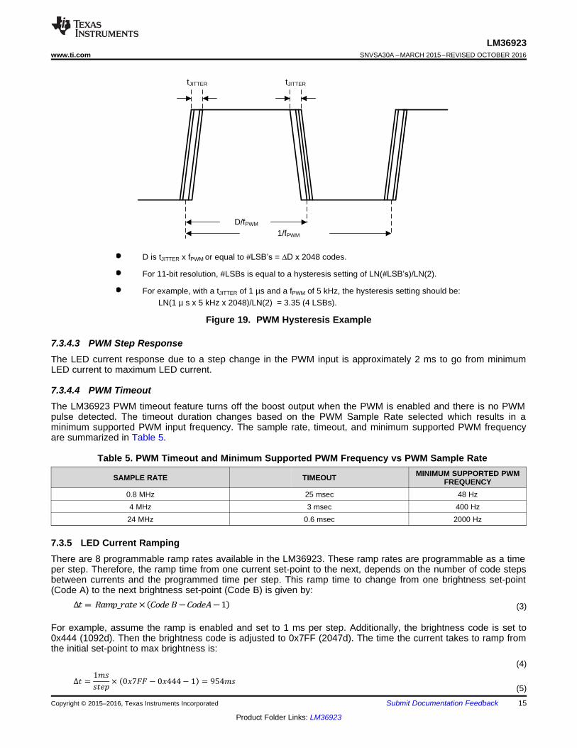
tJITTER
1/fPWM
D/fPWM
x� D is tJITTER x fPWM or equal to #/6%¶V�= ¨'�[�2048 codes.
x� For 11-bit resolution, #LSBs is equal to a hysteresis setting of LN(#/6%¶V)/LN(2).
x� For example, with a tJITTER of 1 µs and a fPWM of 5 kHz, the hysteresis setting should be: LN(1 µ s x 5 kHz x 2048)/LN(2) = 3.35 (4 LSBs).
tJITTER
15
LM36923www.ti.com SNVSA30A –MARCH 2015–REVISED OCTOBER 2016
Product Folder Links: LM36923
Submit Documentation FeedbackCopyright © 2015–2016, Texas Instruments Incorporated
Figure 19. PWM Hysteresis Example
7.3.4.3 PWM Step ResponseThe LED current response due to a step change in the PWM input is approximately 2 ms to go from minimumLED current to maximum LED current.
7.3.4.4 PWM TimeoutThe LM36923 PWM timeout feature turns off the boost output when the PWM is enabled and there is no PWMpulse detected. The timeout duration changes based on the PWM Sample Rate selected which results in aminimum supported PWM input frequency. The sample rate, timeout, and minimum supported PWM frequencyare summarized in Table 5.
Table 5. PWM Timeout and Minimum Supported PWM Frequency vs PWM Sample Rate
SAMPLE RATE TIMEOUT MINIMUM SUPPORTED PWMFREQUENCY
0.8 MHz 25 msec 48 Hz4 MHz 3 msec 400 Hz24 MHz 0.6 msec 2000 Hz
7.3.5 LED Current RampingThere are 8 programmable ramp rates available in the LM36923. These ramp rates are programmable as a timeper step. Therefore, the ramp time from one current set-point to the next, depends on the number of code stepsbetween currents and the programmed time per step. This ramp time to change from one brightness set-point(Code A) to the next brightness set-point (Code B) is given by:
(3)
For example, assume the ramp is enabled and set to 1 ms per step. Additionally, the brightness code is set to0x444 (1092d). Then the brightness code is adjusted to 0x7FF (2047d). The time the current takes to ramp fromthe initial set-point to max brightness is:
(4)
(5)
80
100
120
140
160
180
200
220
240
0.1
0.5
5.0
50.0R
EG
ULA
TE
D H
EA
DR
OO
M V
OLT
AG
E (
V)
LED Current (mA) C001 C001
16
LM36923SNVSA30A –MARCH 2015–REVISED OCTOBER 2016 www.ti.com
Product Folder Links: LM36923
Submit Documentation Feedback Copyright © 2015–2016, Texas Instruments Incorporated
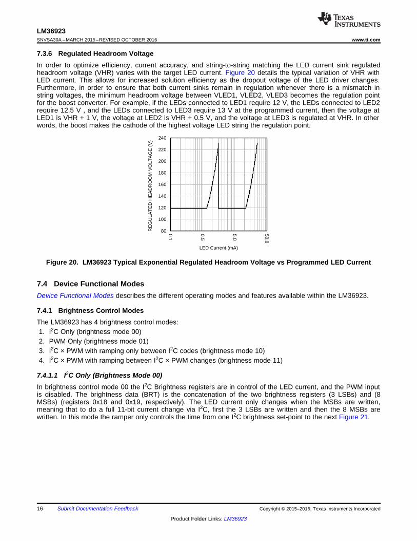
7.3.6 Regulated Headroom VoltageIn order to optimize efficiency, current accuracy, and string-to-string matching the LED current sink regulatedheadroom voltage (VHR) varies with the target LED current. Figure 20 details the typical variation of VHR withLED current. This allows for increased solution efficiency as the dropout voltage of the LED driver changes.Furthermore, in order to ensure that both current sinks remain in regulation whenever there is a mismatch instring voltages, the minimum headroom voltage between VLED1, VLED2, VLED3 becomes the regulation pointfor the boost converter. For example, if the LEDs connected to LED1 require 12 V, the LEDs connected to LED2require 12.5 V , and the LEDs connected to LED3 require 13 V at the programmed current, then the voltage atLED1 is VHR + 1 V, the voltage at LED2 is VHR + 0.5 V, and the voltage at LED3 is regulated at VHR. In otherwords, the boost makes the cathode of the highest voltage LED string the regulation point.
Figure 20. LM36923 Typical Exponential Regulated Headroom Voltage vs Programmed LED Current
7.4 Device Functional ModesDevice Functional Modes describes the different operating modes and features available within the LM36923.
7.4.1 Brightness Control ModesThe LM36923 has 4 brightness control modes:1. I2C Only (brightness mode 00)2. PWM Only (brightness mode 01)3. I2C × PWM with ramping only between I2C codes (brightness mode 10)4. I2C × PWM with ramping between I2C × PWM changes (brightness mode 11)
7.4.1.1 I2C Only (Brightness Mode 00)In brightness control mode 00 the I2C Brightness registers are in control of the LED current, and the PWM inputis disabled. The brightness data (BRT) is the concatenation of the two brightness registers (3 LSBs) and (8MSBs) (registers 0x18 and 0x19, respectively). The LED current only changes when the MSBs are written,meaning that to do a full 11-bit current change via I2C, first the 3 LSBs are written and then the 8 MSBs arewritten. In this mode the ramper only controls the time from one I2C brightness set-point to the next Figure 21.
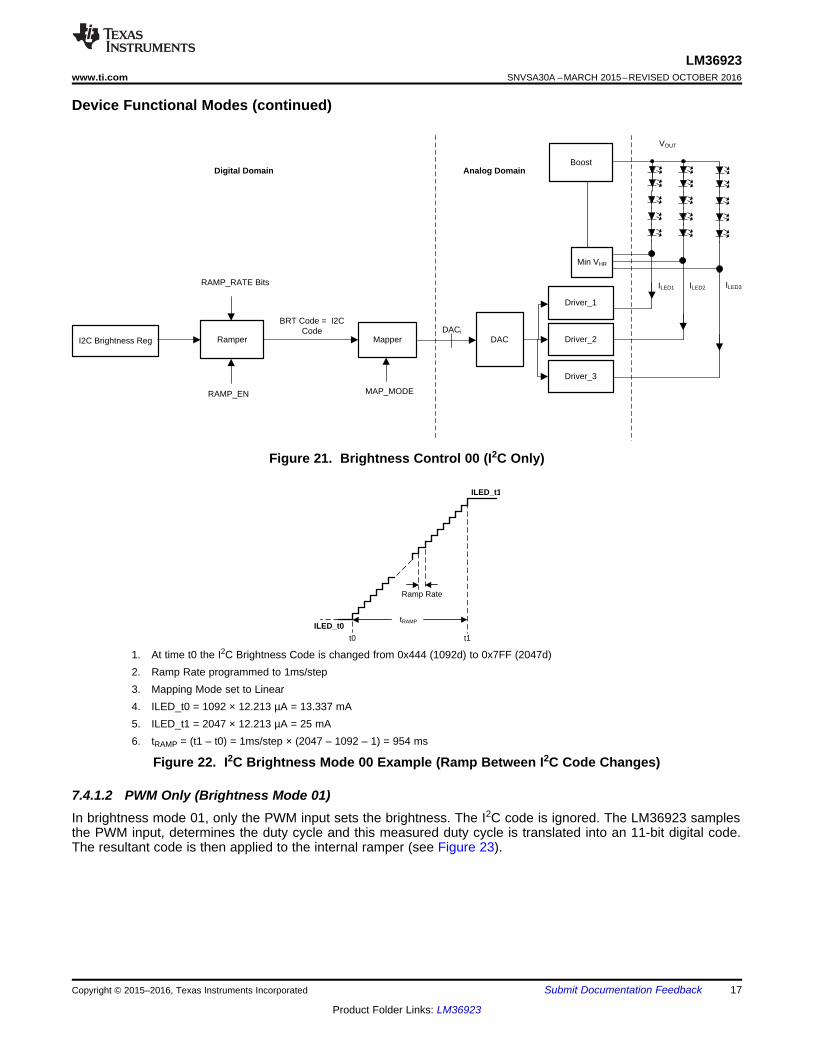
Ramp Rate
ILED_t0
ILED_t1
tRAMP
t1t0
I2C Brightness Reg Ramper Mapper DAC
Driver_1
Driver_2
ILED1 ILED2
Analog DomainDigital DomainBoost
Min VHR
VOUT
DACi
Driver_3
ILED3
RAMP_EN MAP_MODE
RAMP_RATE Bits
BRT Code = I2C Code
17
LM36923www.ti.com SNVSA30A –MARCH 2015–REVISED OCTOBER 2016
Product Folder Links: LM36923
Submit Documentation FeedbackCopyright © 2015–2016, Texas Instruments Incorporated
Device Functional Modes (continued)
Figure 21. Brightness Control 00 (I2C Only)
1. At time t0 the I2C Brightness Code is changed from 0x444 (1092d) to 0x7FF (2047d)2. Ramp Rate programmed to 1ms/step3. Mapping Mode set to Linear4. ILED_t0 = 1092 × 12.213 µA = 13.337 mA5. ILED_t1 = 2047 × 12.213 µA = 25 mA6. tRAMP = (t1 – t0) = 1ms/step × (2047 – 1092 – 1) = 954 ms
Figure 22. I2C Brightness Mode 00 Example (Ramp Between I2C Code Changes)
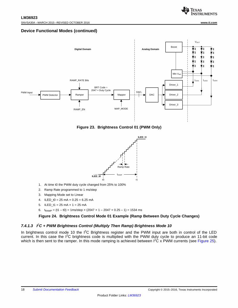
7.4.1.2 PWM Only (Brightness Mode 01)In brightness mode 01, only the PWM input sets the brightness. The I2C code is ignored. The LM36923 samplesthe PWM input, determines the duty cycle and this measured duty cycle is translated into an 11-bit digital code.The resultant code is then applied to the internal ramper (see Figure 23).
Ramp Rate
ILED_t0
ILED_t1
tRAMP
t1t0
PWM Detector Ramper Mapper DAC
Driver_1
Driver_2
ILED1 ILED2
Analog DomainDigital DomainBoost
Min VHR
VOUT
DACi
Driver_3
ILED3
RAMP_EN MAP_MODE
PWM Input
RAMP_RATE Bits
BRT Code =2047 × Duty Cycle
18
LM36923SNVSA30A –MARCH 2015–REVISED OCTOBER 2016 www.ti.com
Product Folder Links: LM36923
Submit Documentation Feedback Copyright © 2015–2016, Texas Instruments Incorporated
Device Functional Modes (continued)
Figure 23. Brightness Control 01 (PWM Only)
1. At time t0 the PWM duty cycle changed from 25% to 100%2. Ramp Rate programmed to 1 ms/step3. Mapping Mode set to Linear4. ILED_t0 = 25 mA × 0.25 = 6.25 mA5. ILED_t1 = 25 mA × 1 = 25 mA6. tRAMP = (t1 – t0) = 1ms/step × (2047 × 1 – 2047 × 0.25 – 1) = 1534 ms
Figure 24. Brightness Control Mode 01 Example (Ramp Between Duty Cycle Changes)
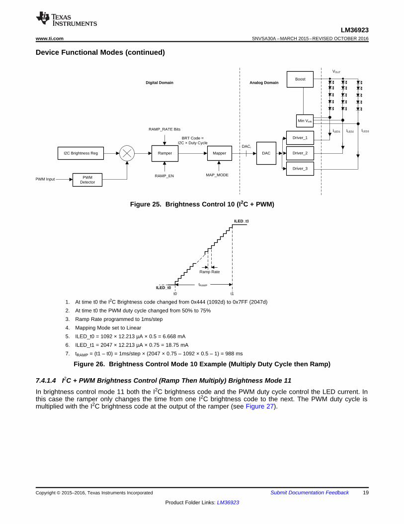
7.4.1.3 I2C + PWM Brightness Control (Multiply Then Ramp) Brightness Mode 10In brightness control mode 10 the I2C Brightness register and the PWM input are both in control of the LEDcurrent. In this case the I2C brightness code is multiplied with the PWM duty cycle to produce an 11-bit codewhich is then sent to the ramper. In this mode ramping is achieved between I2C x PWM currents (see Figure 25).
Ramp Rate
ILED_t0
ILED_t1
tRAMP
t1t0
PWM Detector
Ramper Mapper DAC
Driver_1
Driver_2
ILED1 ILED2
I2C Brightness Reg
Analog DomainDigital DomainBoost
Min VHR
VOUT
DACi
Driver_3
ILED3
RAMP_EN MAP_MODEPWM Input
RAMP_RATE Bits
BRT Code =I2C × Duty Cycle
19
LM36923www.ti.com SNVSA30A –MARCH 2015–REVISED OCTOBER 2016
Product Folder Links: LM36923
Submit Documentation FeedbackCopyright © 2015–2016, Texas Instruments Incorporated
Device Functional Modes (continued)
Figure 25. Brightness Control 10 (I2C + PWM)
1. At time t0 the I2C Brightness code changed from 0x444 (1092d) to 0x7FF (2047d)2. At time t0 the PWM duty cycle changed from 50% to 75%3. Ramp Rate programmed to 1ms/step4. Mapping Mode set to Linear5. ILED_t0 = 1092 × 12.213 µA × 0.5 = 6.668 mA6. ILED_t1 = 2047 × 12.213 µA × 0.75 = 18.75 mA7. tRAMP = (t1 – t0) = 1ms/step × (2047 × 0.75 – 1092 × 0.5 – 1) = 988 ms
Figure 26. Brightness Control Mode 10 Example (Multiply Duty Cycle then Ramp)
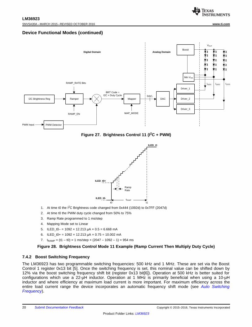
7.4.1.4 I2C + PWM Brightness Control (Ramp Then Multiply) Brightness Mode 11In brightness control mode 11 both the I2C brightness code and the PWM duty cycle control the LED current. Inthis case the ramper only changes the time from one I2C brightness code to the next. The PWM duty cycle ismultiplied with the I2C brightness code at the output of the ramper (see Figure 27).
Ramp Rate
ILED_t0-
ILED_t1
tRAMP
ILED_t0+
t0 t1
PWM Detector
Ramper Mapper DAC
Driver_1
Driver_2
ILED1 ILED2
I2C Brightness Reg
Analog DomainDigital DomainBoost
Min VHR
VOUT
DACi
Driver_3
ILED3
RAMP_EN MAP_MODE
PWM Input
RAMP_RATE Bits
BRT Code =I2C × Duty Cycle
20
LM36923SNVSA30A –MARCH 2015–REVISED OCTOBER 2016 www.ti.com
Product Folder Links: LM36923
Submit Documentation Feedback Copyright © 2015–2016, Texas Instruments Incorporated
Device Functional Modes (continued)
Figure 27. Brightness Control 11 (I2C + PWM)
1. At time t0 the I2C Brightness code changed from 0x444 (1092d) to 0x7FF (2047d)2. At time t0 the PWM duty cycle changed from 50% to 75%3. Ramp Rate programmed to 1 ms/step4. Mapping Mode set to Linear5. ILED_t0– = 1092 × 12.213 µA × 0.5 = 6.668 mA6. ILED_t0+ = 1092 × 12.213 µA × 0.75 = 10.002 mA7. tRAMP = (t1 – t0) = 1 ms/step × (2047 – 1092 – 1) = 954 ms
Figure 28. Brightness Control Mode 11 Example (Ramp Current Then Multiply Duty Cycle)
7.4.2 Boost Switching FrequencyThe LM36923 has two programmable switching frequencies: 500 kHz and 1 MHz. These are set via the BoostControl 1 register 0x13 bit [5]. Once the switching frequency is set, this nominal value can be shifted down by12% via the boost switching frequency shift bit (register 0x13 bit[6]). Operation at 500 kHz is better suited forconfigurations which use a 22-µH inductor. Operation at 1 MHz is primarily beneficial when using a 10-µHinductor and where efficiency at maximum load current is more important. For maximum efficiency across theentire load current range the device incorporates an automatic frequency shift mode (see Auto SwitchingFrequency).
21
LM36923www.ti.com SNVSA30A –MARCH 2015–REVISED OCTOBER 2016
Product Folder Links: LM36923
Submit Documentation FeedbackCopyright © 2015–2016, Texas Instruments Incorporated
Device Functional Modes (continued)7.4.2.1 Minimum Inductor SelectThe LM36923 can use inductors in the range of 10 µH to 22 µH. In order to optimize the converter response tochanges in VIN and load, the Min Inductor Select bit (register 0x13 bit[4]) should be selected depending on whichvalue of inductance is chosen. For 22-µH inductors this bit should be set to 1. For less than 22 µH, this bit shouldbe set to 0.
7.4.3 Auto Switching FrequencyTo take advantage of frequency vs load dependent losses, the LM36923 has the ability to automatically changethe boost switching frequency based on the magnitude of the load current. In addition to the registerprogrammable switching frequencies of 500 kHz and 1 MHz, the auto-frequency mode also incorporates a lowfrequency selection of 250 kHz. It is important to note that the 250-kHz frequency is only accessible in auto-frequency mode and has a maximum boost duty cycle (DMAX) of 50%.
Auto-frequency mode operates by using 2 programmable registers (Auto Frequency High Threshold (register0x15) and Auto Frequency Low Threshold (0x16)). The high threshold determines the switchover from 1 MHz to500 kHz. The low threshold determines the switchover from 500 kHz to 250 kHz. Both the High and LowThreshold registers take an 8-bit code which is compared against the 8 MSB of the brightness register (register0x19). Table 6 details the boundaries for this mode.
Table 6. Auto Switching Frequency OperationBRIGHTNESS CODE MSBs (Register 0x19 bits[7:0]) BOOST SWITCHING FREQUENCY
< Auto Frequency Low Threshold (register 15 Bits[7:0]) 250 kHz (DMAX = 50%)> Auto Frequency Low Threshold (Register 15 Bits[7:0]) or < AutoFrequency High Threshold (Register 14 Bits[7:0])
500 kHz
≥ Auto Frequency High Threshold (register 14 Bits[7:0]) 1 MHz
Automatic-frequency mode is enabled whenever there is a non-zero code in either the Auto-Frequency High orAuto-Frequency Low registers. To disable the auto-frequency shift mode, set both registers to 0x00. Whenautomatic-frequency select mode is disabled, the switching frequency operates at the programmed frequency(Register 0x13 bit[5]) across the entire LED current range. Table 7 provides a guideline for selecting the autofrequency 250-kHz threshold setting, the actual setting needs to be verified in the application.
Table 7. Auto Frequency 250-kHz Threshold SettingsCONDITION
(Vf=3.2 V,ILED=25 mA)
INDUCTOR(µH)
RECOMMENDED AUTO FREQUENCYLOW THRESHOLD MAXIMUM VALUE
(NO SHIFT)
OUTPUT POWER AT AUTOFREQUENCY SWITCHOVER
(W)3 × 4 LEDs 10 0x17 0.0793 × 5 LEDs 10 0x15 0.0893 × 6 LEDs 10 0x13 0.0973 × 7 LEDs 10 0x11 0.1013 × 8 LEDs 10 0x0f 0.102
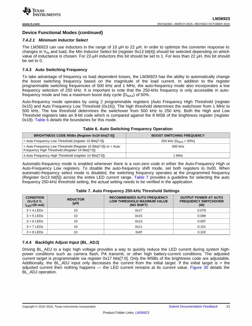
7.4.4 Backlight Adjust Input (BL_ADJ)Driving BL_ADJ to a logic high voltage provides a way to quickly reduce the LED current during system high-power conditions such as camera flash, PA transmit, or other high battery-current conditions. The adjustedcurrent target is programmable via register 0x17 bits[7:0]. Only the MSBs of the brightness code are adjustable.Additionally, the BL_ADJ input only decreases the current from the initial target. If the initial target is > theadjusted current then nothing happens — the LED current remains at its current value. Figure 30 details theBL_ADJ operation.
tBRT_DAC
BL_ADJ
ILED
ILED_BRT
ILED_ADJ
tBRT_DAC
tDAC_LED
Mapper DAC
Driver_1
Driver_2
ILED1 ILED2
Analog DomainDigital DomainBoost
Min VHR
VOUT
DACi
Driver_3
ILED3
MAP_MODE
BRT Code (I2C and/or PWM)
BL_ADJ
Backlight AdjustThreshold [10:3] + 3 /6%¶V�VHW�WR�000
11
11
11
Active High/Active Low
Polarity Bit
22
LM36923SNVSA30A –MARCH 2015–REVISED OCTOBER 2016 www.ti.com
Product Folder Links: LM36923
Submit Documentation Feedback Copyright © 2015–2016, Texas Instruments Incorporated
Figure 29. Backlight Adjust Operation
LED Current operates at an initial target ILED_BRT which is set by either I2C or PWM (or both).When the BL_ADJ input is driven to a logic high the LM36923's brightness code at the Mapper input has the MSBsset to the BL_ADJ Threshold and the LSBs set to 000.ILED steps down to the new target current in < 50 µs.When BL_ADJ is forced low the LED current returns to the initial brightness target.
Figure 30. Backlight Adjust Timing
7.4.4.1 Back-Light Adjust Input PolarityThe BL_ADJ input can have either active high or active low polarity. With active high polarity (default), driving theBL_ADJ input high forces the LED current to the BL_ADJ low target current. With active low polarity, driving theBL_ADJ input low forces the LED current to the BL_ADJ low target current. The polarity is set via bit 0 in register11.

23
LM36923www.ti.com SNVSA30A –MARCH 2015–REVISED OCTOBER 2016
Product Folder Links: LM36923
Submit Documentation FeedbackCopyright © 2015–2016, Texas Instruments Incorporated
7.4.5 Fault Protection/Detection
7.4.5.1 Overvoltage Protection (OVP)The LM36923 provides four OVP thresholds (17 V, 21 V, 25 V, and 29 V). The OVP circuitry monitors the boostoutput voltage (VOUT) and protects OUT and SW from exceeding safe operating voltages in case of open loadconditions or in the event the LED string voltage requires more voltage than the programmed OVP setting. TheOVP thresholds are programmed in register 13 bits[3:2]. The operation of OVP differentiates between twoovervoltage conditions and responds differently as outlined below:
7.4.5.1.1 Case 1 OVP Fault Only (OVP Threshold Hit and All Enabled Current Sink Inputs > 40 mV)
In steady-state operation with VOUT near the OVP threshold a rapid change in VIN or brightness code can result ina momentary transient excursion of VOUT above the OVP threshold. In this case the boost circuitry is disableduntil VOUT drops below OVP – hysteresis (1 V). Once this happens the boost is re-enabled and steady stateregulation continues. If VOUT remains above the OVP threshold for > 1 ms the OVP Flag is set (register 0x1Fbit[0]).
7.4.5.1.2 Case 2a OVP Fault and Open LED String Fault (OVP Threshold Occurrence and Any Enabled Current SinkInput ≤ 40 mV)
When any of the enabled LED strings is open the boost converter tries to drive VOUT above OVP and at the sametime the open string(s) current sink headroom voltage(s) (LED1, LED2, LED3) drop to 0. When the LM36923detects three occurrences of VOUT > OVP and any enabled current sink input (VLED1 or VLED2, VLED3) ≤ 40 mV,the OVP Fault flag is set (register 0x1F bit[0]), and the LED Open Fault flag is set (register 0x1F bit[4]).
7.4.5.1.3 Case 2b OVP Fault and Open LED String Fault (OVP Threshold Duration and Any Enabled Current SinkInput ≤ 40 mV)
When any of the enabled LED strings is open the boost converter tries to drive VOUT above OVP and at the sametime the open string(s) current sink headroom voltage(s) (LED1, LED2, LED3) drop to 0. When the LM36923detects VOUT > OVP for > 1 msec and any enabled current sink input (VLED1 or VLED2, VLED3) ≤ 40 mV, the OVPFault flag is set (register 0x1F bit[0]), and the LED Open Fault flag is set (register 0x1F bit[4]).
7.4.5.1.4 OVP/LED Open Fault Shutdown
The LM36923 has the option of shutting down the device when the OVP flag is set. This option can be enabledor disabled via register 0x1E bit[0]. When the shutdown option is disabled the fault flag is a report only. When thedevice is shut down due to an OVP/LED String Open fault, the fault flags register must be read back before theLM36923 can be re-enabled.
7.4.5.1.5 Testing for LED String Open
The procedure for detecting an open in a LED string is:• Apply power the the LM36923.• Enable all LED strings (Register 0x10 = 0x0F).• Set maximum brightness (Register 0x18 = 0x07 and Register 0x19 = 0xFF).• Set the brightness control (Register 0x11 = 0x00).• Open LED1 string.• Wait 4 msec.• Read LED open fault (Register 0x1F).• If bit[4] = 1, then a LED open fault condition has been detected.• Connect LED1 string.• Repeat the procedure for the other LED strings.
24
LM36923SNVSA30A –MARCH 2015–REVISED OCTOBER 2016 www.ti.com
Product Folder Links: LM36923
Submit Documentation Feedback Copyright © 2015–2016, Texas Instruments Incorporated
7.4.5.2 LED String Short FaultThe LM36923 can detect an LED string short fault. This happens when the voltage between VIN and any enabledcurrent sink input has dropped below (1.5 V). This test can only be performed on one LED string at a time.Performing this test with more than one LED string enabled can result in a faulty reading. The procedure fordetecting a short in a LED string is:• Apply power the the LM36923.• Enable only LED1 string (Register 0x10 = 0x03).• Enable short fault (Register 0x1E = 0x01.• Set maximum brightness (Register 0x18 = 0x07 and Register 0x19 = 0xFF).• Set the brightness control (Register 0x11 = 0x00).• Wait 4 msec.• Read LED short fault (Register 0x1F).• If bit[3] = 1, then a LED short fault condition has been detected.• Set chip enable and LED string enable low (Register 0x10 = 0x00).• Repeat the procedure for the other LED strings.
7.4.5.3 Overcurrent Protection (OCP)The LM36923 has 4 selectable OCP thresholds (750 mA, 1000 mA, 1250 mA, and 1500 mA). These areprogrammable in register 0x13 bits[1:0]. The OCP threshold is a cycle-by-cycle current limit and is detected inthe internal low-side NFET. Once the threshold is hit the NFET turns off for the remainder of the switching period.
7.4.5.3.1 OCP Fault
If enough overcurrent threshold events occur, the OCP Flag (register 0x1F bit[1]) is set. To avoid transientconditions from inadvertently setting the OCP Flag, a pulse density counter monitors OCP threshold events overa 128-µs period. If 8 consecutive 128-µs periods occur where the pulse density count has found 2 or more OCPevents,then the OCP Flag is set.
During device start-up and during brightness code changes, there is a 4-ms blank time where OCP events areignored. As a result, if the device starts up in an overcurrent condition there is an approximate 5-ms delay beforethe OCP Flag is set.
7.4.5.3.2 OCP Shutdown
The LM36923 has the option of shutting down the device when the OCP flag is set. This option can be enabledor disabled via register 0x1E bit[1]. When the shutdown option is disabled, the fault flag is a report only. Whenthe device is shut down due to an OCP fault, the fault flags register must be read back before the LM36923 canbe re-enabled.
7.4.5.4 Device Overtemperature (TSD)Thermal shutdown (TSD) is triggered when the device die temperature reaches 135˚C. When this happens theboost stops switching, and the TSD Flag (register 0x1F bit[2]) is set. The boost automatically starts up againwhen the die temperature cools down to 120˚C.
7.4.5.4.1 Overtemperature Shutdown
The LM36923 has the option of shutting down the device when the TSD flag is set. This option can be enabledor disabled via register 0x1E bit[2]. When the shutdown option is disabled the fault flag is a report only. When thedevice is shutdown due to a TSD fault, the Fault Flags register must be read back before the LM36923 can bere-enabled.
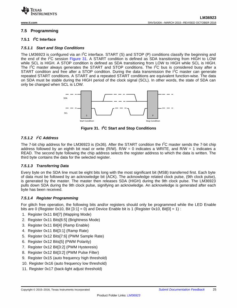
Start Condition Stop Condition
SDA
SCL
S P
25
LM36923www.ti.com SNVSA30A –MARCH 2015–REVISED OCTOBER 2016
Product Folder Links: LM36923
Submit Documentation FeedbackCopyright © 2015–2016, Texas Instruments Incorporated
7.5 Programming
7.5.1 I2C Interface
7.5.1.1 Start and Stop ConditionsThe LM36923 is configured via an I2C interface. START (S) and STOP (P) conditions classify the beginning andthe end of the I2C session Figure 31. A START condition is defined as SDA transitioning from HIGH to LOWwhile SCL is HIGH. A STOP condition is defined as SDA transitioning from LOW to HIGH while SCL is HIGH.The I2C master always generates the START and STOP conditions. The I2C bus is considered busy after aSTART condition and free after a STOP condition. During the data transmission the I2C master can generaterepeated START conditions. A START and a repeated START conditions are equivalent function-wise. The dataon SDA must be stable during the HIGH period of the clock signal (SCL). In other words, the state of SDA canonly be changed when SCL is LOW.
Figure 31. I2C Start and Stop Conditions
7.5.1.2 I2C AddressThe 7-bit chip address for the LM36923 is (0x36). After the START condition the I2C master sends the 7-bit chipaddress followed by an eighth bit read or write (R/W). R/W = 0 indicates a WRITE, and R/W = 1 indicates aREAD. The second byte following the chip address selects the register address to which the data is written. Thethird byte contains the data for the selected register.
7.5.1.3 Transferring DataEvery byte on the SDA line must be eight bits long with the most significant bit (MSB) transferred first. Each byteof data must be followed by an acknowledge bit (ACK). The acknowledge related clock pulse, (9th clock pulse),is generated by the master. The master then releases SDA (HIGH) during the 9th clock pulse. The LM36923pulls down SDA during the 9th clock pulse, signifying an acknowledge. An acknowledge is generated after eachbyte has been received.
7.5.1.4 Register ProgrammingFor glitch free operation, the following bits and/or registers should only be programmed while the LED Enablebits are 0 (Register 0x10, Bit [3:1] = 0) and Device Enable bit is 1 (Register 0x10, Bit[0] = 1) :1. Register 0x11 Bit[7] (Mapping Mode)2. Register 0x11 Bits[6:5] (Brightness Mode)3. Register 0x11 Bit[4] (Ramp Enable)4. Register 0x11 Bit[3:1] (Ramp Rate)5. Register 0x12 Bits[7:6] (PWM Sample Rate)6. Register 0x12 Bits[5] (PWM Polarity)7. Register 0x12 Bit[3:2] (PWM Hysteresis)8. Register 0x12 Bit[3:2] (PWM Pulse Filter)9. Register 0x15 (auto frequency high threshold)10. Register 0x16 (auto frequency low threshold)11. Register 0x17 (back-light adjust threshold)
26
LM36923SNVSA30A –MARCH 2015–REVISED OCTOBER 2016 www.ti.com
Product Folder Links: LM36923
Submit Documentation Feedback Copyright © 2015–2016, Texas Instruments Incorporated
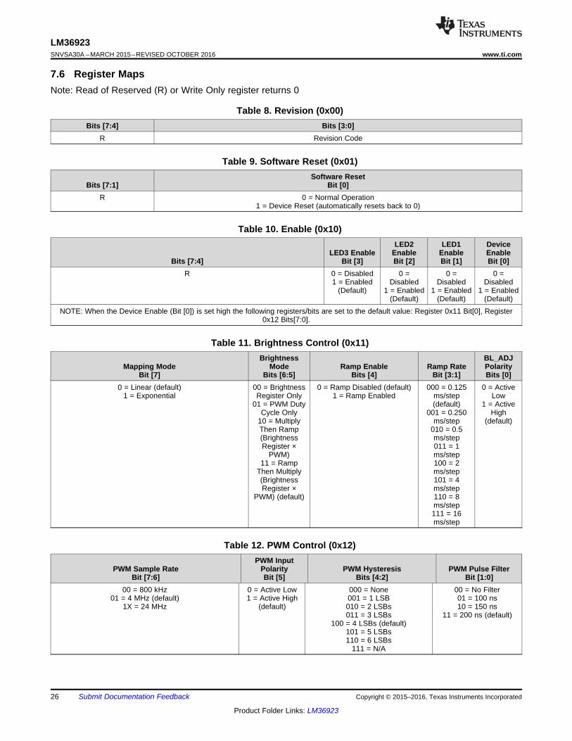
7.6 Register MapsNote: Read of Reserved (R) or Write Only register returns 0
Table 8. Revision (0x00)Bits [7:4] Bits [3:0]
R Revision Code
Table 9. Software Reset (0x01)
Bits [7:1]Software Reset
Bit [0]R 0 = Normal Operation
1 = Device Reset (automatically resets back to 0)
Table 10. Enable (0x10)
Bits [7:4]LED3 Enable
Bit [3]
LED2EnableBit [2]
LED1EnableBit [1]
DeviceEnableBit [0]
R 0 = Disabled1 = Enabled
(Default)
0 =Disabled
1 = Enabled(Default)
0 =Disabled
1 = Enabled(Default)
0 =Disabled
1 = Enabled(Default)
NOTE: When the Device Enable (Bit [0]) is set high the following registers/bits are set to the default value: Register 0x11 Bit[0], Register0x12 Bits[7:0].
Table 11. Brightness Control (0x11)
Mapping ModeBit [7]
BrightnessMode
Bits [6:5]Ramp Enable
Bits [4]Ramp Rate
Bit [3:1]
BL_ADJPolarityBits [0]
0 = Linear (default)1 = Exponential
00 = BrightnessRegister Only
01 = PWM DutyCycle Only
10 = MultiplyThen Ramp(BrightnessRegister ×
PWM)11 = Ramp
Then Multiply(BrightnessRegister ×
PWM) (default)
0 = Ramp Disabled (default)1 = Ramp Enabled
000 = 0.125ms/step(default)
001 = 0.250ms/step
010 = 0.5ms/step011 = 1ms/step100 = 2ms/step101 = 4ms/step110 = 8ms/step111 = 16ms/step
0 = ActiveLow
1 = ActiveHigh
(default)
Table 12. PWM Control (0x12)
PWM Sample RateBit [7:6]
PWM InputPolarityBit [5]
PWM HysteresisBits [4:2]
PWM Pulse FilterBit [1:0]
00 = 800 kHz01 = 4 MHz (default)
1X = 24 MHz
0 = Active Low1 = Active High
(default)
000 = None001 = 1 LSB010 = 2 LSBs011 = 3 LSBs
100 = 4 LSBs (default)101 = 5 LSBs110 = 6 LSBs
111 = N/A
00 = No Filter01 = 100 ns10 = 150 ns
11 = 200 ns (default)
27
LM36923www.ti.com SNVSA30A –MARCH 2015–REVISED OCTOBER 2016
Product Folder Links: LM36923
Submit Documentation FeedbackCopyright © 2015–2016, Texas Instruments Incorporated
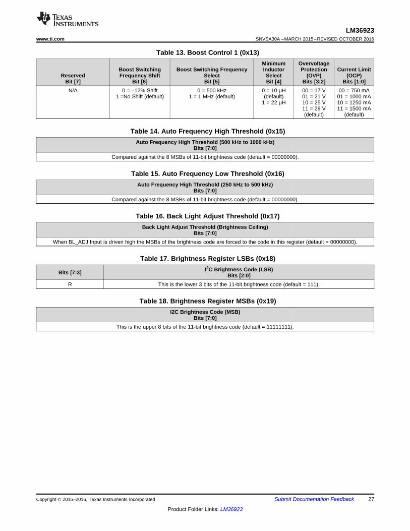
Table 13. Boost Control 1 (0x13)
ReservedBit [7]
Boost SwitchingFrequency Shift
Bit [6]
Boost Switching FrequencySelectBit [5]
MinimumInductorSelectBit [4]
OvervoltageProtection
(OVP)Bits [3:2]
Current Limit(OCP)
Bits [1:0]N/A 0 = –12% Shift
1 =No Shift (default)0 = 500 kHz
1 = 1 MHz (default)0 = 10 µH(default)
1 = 22 µH
00 = 17 V01 = 21 V10 = 25 V11 = 29 V(default)
00 = 750 mA01 = 1000 mA10 = 1250 mA11 = 1500 mA
(default)
Table 14. Auto Frequency High Threshold (0x15)Auto Frequency High Threshold (500 kHz to 1000 kHz)
Bits [7:0]Compared against the 8 MSBs of 11-bit brightness code (default = 00000000).
Table 15. Auto Frequency Low Threshold (0x16)Auto Frequency High Threshold (250 kHz to 500 kHz)
Bits [7:0]Compared against the 8 MSBs of 11-bit brightness code (default = 00000000).
Table 16. Back Light Adjust Threshold (0x17)Back Light Adjust Threshold (Brightness Ceiling)
Bits [7:0]When BL_ADJ Input is driven high the MSBs of the brightness code are forced to the code in this register (default = 00000000).
Table 17. Brightness Register LSBs (0x18)
Bits [7:3] I2C Brightness Code (LSB)Bits [2:0]
R This is the lower 3 bits of the 11-bit brightness code (default = 111).
Table 18. Brightness Register MSBs (0x19)I2C Brightness Code (MSB)
Bits [7:0]This is the upper 8 bits of the 11-bit brightness code (default = 11111111).
28
LM36923SNVSA30A –MARCH 2015–REVISED OCTOBER 2016 www.ti.com
Product Folder Links: LM36923
Submit Documentation Feedback Copyright © 2015–2016, Texas Instruments Incorporated
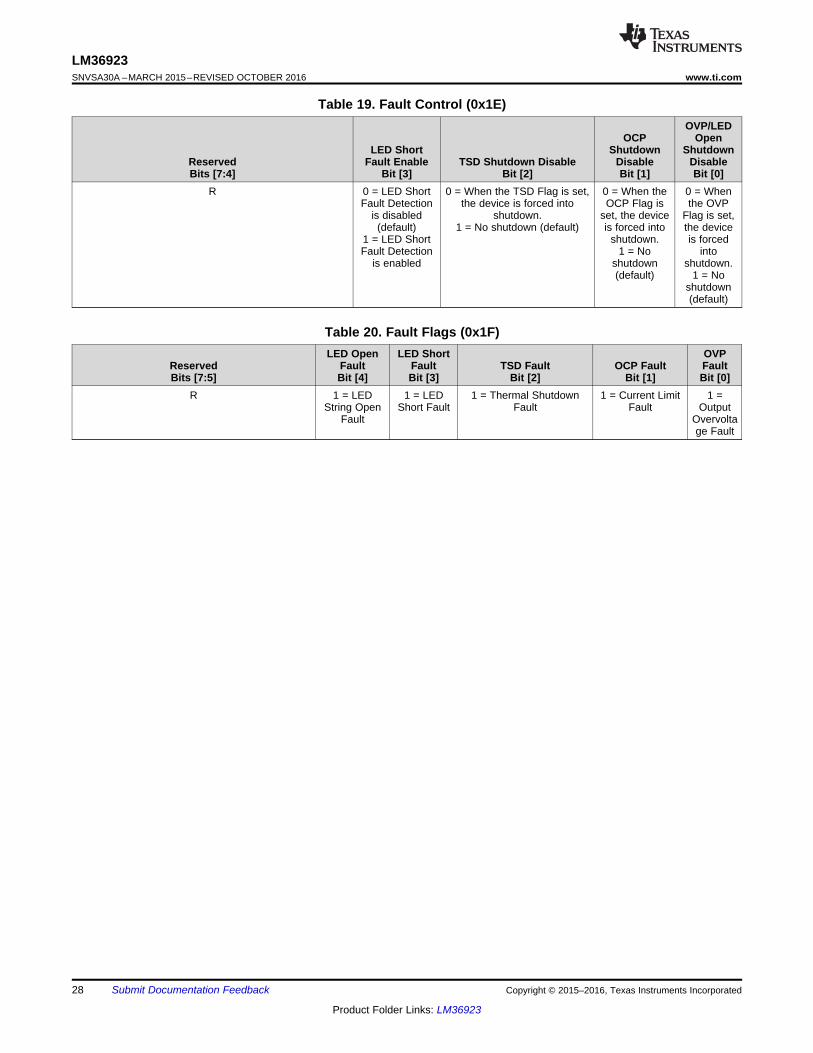
Table 19. Fault Control (0x1E)
ReservedBits [7:4]
LED ShortFault Enable
Bit [3]TSD Shutdown Disable
Bit [2]
OCPShutdown
DisableBit [1]
OVP/LEDOpen
ShutdownDisableBit [0]
R 0 = LED ShortFault Detection
is disabled(default)
1 = LED ShortFault Detection
is enabled
0 = When the TSD Flag is set,the device is forced into
shutdown.1 = No shutdown (default)
0 = When theOCP Flag is
set, the deviceis forced into
shutdown.1 = No
shutdown(default)
0 = Whenthe OVP
Flag is set,the deviceis forced
intoshutdown.
1 = Noshutdown(default)
Table 20. Fault Flags (0x1F)
ReservedBits [7:5]
LED OpenFaultBit [4]
LED ShortFaultBit [3]
TSD FaultBit [2]
OCP FaultBit [1]
OVPFaultBit [0]
R 1 = LEDString Open
Fault
1 = LEDShort Fault
1 = Thermal ShutdownFault
1 = Current LimitFault
1 =Output
Overvoltage Fault
29
LM36923www.ti.com SNVSA30A –MARCH 2015–REVISED OCTOBER 2016
Product Folder Links: LM36923
Submit Documentation FeedbackCopyright © 2015–2016, Texas Instruments Incorporated
8 Applications and Implementation
NOTEInformation in the following applications sections is not part of the TI componentspecification, and TI does not warrant its accuracy or completeness. TI’s customers areresponsible for determining suitability of components for their purposes. Customers shouldvalidate and test their design implementation to confirm system functionality.
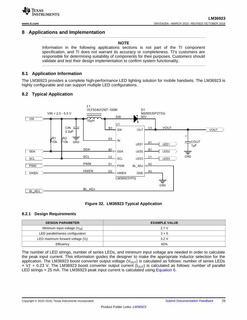
8.1 Application InformationThe LM36923 provides a complete high-performance LED lighting solution for mobile handsets. The LM36923 ishighly configurable and can support multiple LED configurations.
8.2 Typical Application
Figure 32. LM36923 Typical Application
8.2.1 Design Requirements
DESIGN PARAMETER EXAMPLE VALUEMinimum input voltage (VIN) 2.7 V
LED parallel/series configuration 3 × 5LED maximum forward voltage (Vf) 3.2 V
Efficiency 82%
The number of LED strings, number of series LEDs, and minimum input voltage are needed in order to calculatethe peak input current. This information guides the designer to make the appropriate inductor selection for theapplication. The LM36923 boost converter output voltage (VOUT) is calculated as follows: number of series LEDs× Vƒ + 0.23 V. The LM36923 boost converter output current (IOUT) is calculated as follows: number of parallelLED strings × 25 mA. The LM36923 peak input current is calculated using Equation 6.
&% 8KHP=CA &AN=PEJC R 0.38µ(
:1F 6KH;× :1F6AIL_?K;
+2'#- = 8176 × +176
8+0 ×K+
8+0
2 × B59 × .× l1 +
8+0 ×K
8176p
30
LM36923SNVSA30A –MARCH 2015–REVISED OCTOBER 2016 www.ti.com
Product Folder Links: LM36923
Submit Documentation Feedback Copyright © 2015–2016, Texas Instruments Incorporated
8.2.2 Detailed Design Procedure
Table 21. Typical Application Component ListCONFIGURATION L1 D1 COUT
3p7s, 3p8s VLF504012MT-100MVLF504012MT-150M NSR0530P2T5G C2012X7R1H105K085AC
3p6s VLF504012MT-220M NSR0530P2T5G C2012X7R1H105K085AC3p5s VLF403210MT-100M NSR0530P2T5G C2012X7R1H105K085AC3p4s VLF302510MT-100M NSR0530P2T5G C2012X7R1H105K085AC
8.2.2.1 Component Selection
8.2.2.1.1 Inductor
The LM36923 requires a typical inductance in the range of 10 µH to 22 µH. When selecting the inductor, ensurethat the saturation rating for the inductor is high enough to accommodate the peak inductor current of theapplication (IPEAK) given in the inductor datasheet. The peak inductor current occurs at the maximum loadcurrent, the maximum output voltage, the minimum input voltage, and the minimum switching frequency setting.Also, the peak current requirement increases with decreasing efficiency. IPEAK can be estimated usingEquation 6:
(6)
Also, the peak current calculated above is different from the peak inductor current setting (ISAT). The NMOSswitch current limit setting (ICL_MIN) must be greater than IPEAK from Equation 6 above.
8.2.2.1.2 Output Capacitor
The LM36923 requires a ceramic capacitor with a minimum of 0.4 µF of capacitance at the output, specified overthe entire range of operation. This ensures that the device remains stable and oscillation free. The 0.4 µF ofcapacitance is the minimum amount of capacitance, which is different than the value of capacitor. Capacitancewould take into account tolerance, temperature, and DC voltage shift.
Table 22 lists possible output capacitors that can be used with the LM36923. Figure 33 shows the DC bias of thefour TDK capacitors. The useful voltage range is determined from the effective output voltage range for a givencapacitor as determined by Equation 7:
(7)
Table 22. Recommended Output Capacitors
PART NUMBER MANUFACTURER CASESIZE
VOLTAGERATING (V)
NOMINALCAPACITANCE
(µF)TOLERANCE (%) TEMPERATURE
COEFFICIENT (%)
RECOMMENDED MAXOUTPUT VOLTAGE
(FOR SINGLECAPACITOR)
C2012X5R1H105K085AB TDK 0805 50 1 ±10 ±15 22
C2012X5R1H225K085AB TDK 0805 50 2.2 ±10 ±15 24
C1608X5R1V225K080AC TDK 0603 35 2.2 ±10 ±15 12
C1608X5R1H105K080AB TDK 0603 50 1 ±10 ±15 15
For example, with a 10% tolerance, and a 15% temperature coefficient, the DC voltage derating must be ≥0.38/(0.9 × 0.85) = 0.5 µF. For the C1608X5R1H225K080AB (0603, 50-V) device, the useful voltage rangeoccurs up to the point where the DC bias derating falls below 0.523 µF, or around 12 V. For configurations whereVOUT is > 15 V, two of these capacitors can be paralleled, or a larger capacitor such as theC2012X5R1H105K085AB must be used.
60%
65%
70%
75%
80%
85%
90%
95%
0 10 20 30 40 50 60 70 80
BO
OS
T E
FF
ICIE
NC
Y
LED CURRENT (mA)
3p4s
3p5s
3p6s
3p7s
3p8s
C001
Three String, AF Enabled, 10 uH, 3.7V
60%
65%
70%
75%
80%
85%
90%
95%
0 10 20 30 40 50 60
BO
OS
T E
FF
ICIE
NC
Y
LED CURRENT (mA)
2p4s
2p5s
2p6s
2p7s
2p8s
C001
Two String, AF Enabled, 10 uH, 3.7V
00.10.20.30.40.50.60.70.80.9
11.11.21.31.41.51.61.71.81.9
2
0 2 4 6 8 10 12 14 16 18 20 22 24 26 28
Cap
acita
nce
(µF
)
DC Bias
C2012X5R1H105K085AB
C2012X5R1H225K085AB
C1608X5R1V225K080AC
C1608X5R1H105K080AB
C006
31
LM36923www.ti.com SNVSA30A –MARCH 2015–REVISED OCTOBER 2016
Product Folder Links: LM36923
Submit Documentation FeedbackCopyright © 2015–2016, Texas Instruments Incorporated
Figure 33. DC Bias Derating for 0805 Case Size and0603 Case Size 35-V and 50-V Ceramic Capacitors
8.2.2.1.3 Input Capacitor
The input capacitor in a boost is not as critical as the output capacitor. The input capacitor primary function is tofilter the switching supply currents at the device input and to filter the inductor current ripple at the input of theinductor. The recommended input capacitor is a 2.2-µF ceramic (0402, 10-V device) or equivalent.
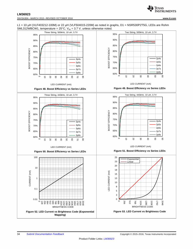
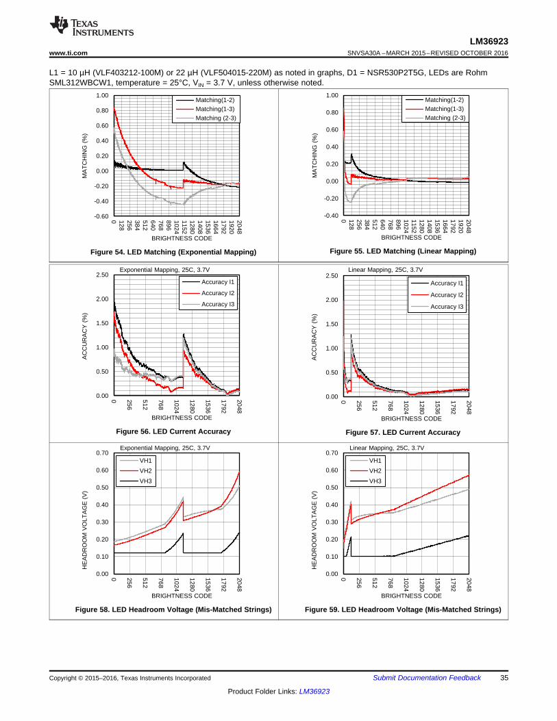
8.2.3 Application CurvesL1 = 10 µH (VLF403212-100M) or 22 µH (VLF504015-220M) as noted in graphs, D1 = NSR530P2T5G, LEDs are RohmSML312WBCW1, temperature = 25°C, VIN = 3.7 V, unless otherwise noted.
Figure 34. Boost Efficiency vs Series LEDs Figure 35. Boost Efficiency vs Series LEDs
65%
70%
75%
80%
85%
90%
95%
0 10 20 30 40 50 60 70 80
BO
OS
T E
FF
ICIE
NC
Y
LED CURRENT (mA)
3p8s
3p7s
3p6s
3p5s
3p4s
C001
Three String, 500kHz, 22 uH, 3.7V
65%
70%
75%
80%
85%
90%
95%
0 10 20 30 40 50
BO
OS
T E
FF
ICIE
NC
Y
LED CURRENT (mA)
2p8s
2p7s
2p6s
2p5s
2p4s
C001
Two String, 500kHz, 22 uH, 3.7V
65%
70%
75%
80%
85%
90%
95%
0 10 20 30 40 50 60 70 80
BO
OS
T E
FF
ICIE
NC
Y
LED CURRENT (mA)
3p8s
3p7s
3p6s
3p5s
3p4s
C001
Three String, 443kHz, 22 uH, 3.7V
65%
70%
75%
80%
85%
90%
95%
0 10 20 30 40 50
BO
OS
T E
FF
ICIE
NC
Y
LED CURRENT (mA)
2p8s
2p7s
2p6s
2p5s
2p4s
C001
Two String, 443kHz, 22 uH, 3.7V
60%
65%
70%
75%
80%
85%
90%
95%
0 10 20 30 40 50 60 70 80
BO
OS
T E
FF
ICIE
NC
Y
LED CURRENT (mA)
3p4s
3p5s
3p6s
3p7s
3p8s
C001
Three String, AF Enabled -12%, 10 uH, 3.7V
60%
65%
70%
75%
80%
85%
90%
95%
0 10 20 30 40 50 60
BO
OS
T E
FF
ICIE
NC
Y
LED CURRENT (mA)
2p4s
2p5s
2p6s
2p7s
2p8s
C001
Two String, AF Enabled -12%, 10 uH, 3.7V
32
LM36923SNVSA30A –MARCH 2015–REVISED OCTOBER 2016 www.ti.com
Product Folder Links: LM36923
Submit Documentation Feedback Copyright © 2015–2016, Texas Instruments Incorporated
L1 = 10 µH (VLF403212-100M) or 22 µH (VLF504015-220M) as noted in graphs, D1 = NSR530P2T5G, LEDs are RohmSML312WBCW1, temperature = 25°C, VIN = 3.7 V, unless otherwise noted.
Figure 36. Boost Efficiency vs Series LEDs Figure 37. Boost Efficiency vs Series LEDs
Figure 38. Boost Efficiency vs Series LEDs Figure 39. Boost Efficiency vs Series LEDs
Figure 40. Boost Efficiency vs Series LEDs Figure 41. Boost Efficiency vs Series LEDs
60%
65%
70%
75%
80%
85%
90%
95%
0 10 20 30 40 50 60 70 80
BO
OS
T E
FF
ICIE
NC
Y
LED CURRENT (mA)
3p4s
3p5s
3p6s
3p7s
3p8s
C001
Three String, 887kHz, 10 uH, 3.7V
60%
65%
70%
75%
80%
85%
90%
95%
0 10 20 30 40 50 60
BO
OS
T E
FF
ICIE
NC
Y
LED CURRENT (mA)
2p4s
2p5s
2p6s
2p7s
2p8s
C001
Two String, 887kHz, 10 uH, 3.7V
60%
65%
70%
75%
80%
85%
90%
95%
0 10 20 30 40 50 60 70 80
BO
OS
T E
FF
ICIE
NC
Y
LED CURRENT (mA)
3p4s
3p5s
3p6s
3p7s
3p8s
C001
Three String, 1Mhz, 10 uH, 3.7V
60%
65%
70%
75%
80%
85%
90%
95%
0 10 20 30 40 50 60
BO
OS
T E
FF
ICIE
NC
Y
LED CURRENT (mA)
2p4s
2p5s
2p6s
2p7s
2p8s
C001
Two String, 1Mhz, 10 uH, 3.7V
65%
70%
75%
80%
85%
90%
95%
0 10 20 30 40 50 60 70 80
BO
OS
T E
FF
ICIE
NC
Y
LED CURRENT (mA)
3p8s
3p7s
3p6s
3p5s
3p4s
C001
Three String, 887kHz, 22 uH, 3.7V
65%
70%
75%
80%
85%
90%
95%
0 10 20 30 40 50
BO
OS
T E
FF
ICIE
NC
Y
LED CURRENT (mA)
2p8s
2p7s
2p6s
2p5s
2p4s
C001
Two String, 887kHz, 22 uH, 3.7V
33
LM36923www.ti.com SNVSA30A –MARCH 2015–REVISED OCTOBER 2016
Product Folder Links: LM36923
Submit Documentation FeedbackCopyright © 2015–2016, Texas Instruments Incorporated
L1 = 10 µH (VLF403212-100M) or 22 µH (VLF504015-220M) as noted in graphs, D1 = NSR530P2T5G, LEDs are RohmSML312WBCW1, temperature = 25°C, VIN = 3.7 V, unless otherwise noted.
Figure 42. Boost Efficiency vs Series LEDs Figure 43. Boost Efficiency vs Series LEDs
Figure 44. Boost Efficiency vs Series LEDs Figure 45. Boost Efficiency vs Series LEDs
Figure 46. Boost Efficiency vs Series LEDs Figure 47. Boost Efficiency vs Series LEDs
0.01
0.1
1
10
100
0 128256384512640768896102411521280140815361664179219202048
CU
RR
EN
T (
mA
)
BRIGHTNESS CODE C001
0
3
5
8
10
13
15
18
20
23
25
0 256
512
768
1024
1280
1536
1792
2048
LED
CU
RR
EN
T (
mA
)
BRIGHTNESS CODE
ExponentialLinear
C001
60%
65%
70%
75%
80%
85%
90%
95%
0 10 20 30 40 50 60 70 80
BO
OS
T E
FF
ICIE
NC
Y
LED CURRENT (mA)
3p4s
3p5s
3p6s
3p7s
3p8s
C001
Three String, 443kHz, 10 uH, 3.7V
60%
65%
70%
75%
80%
85%
90%
95%
0 10 20 30 40 50 60
BO
OS
T E
FF
ICIE
NC
Y
LED CURRENT (mA)
2p4s
2p5s
2p6s
2p7s
2p8s
C001
Two String, 443kHz, 10 uH, 3.7V
60%
65%
70%
75%
80%
85%
90%
95%
0 10 20 30 40 50 60 70 80
BO
OS
T E
FF
ICIE
NC
Y
LED CURRENT (mA)
3p4s
3p5s
3p6s
3p7s
3p8s
C001
Three String, 500kHz, 10 uH, 3.7V
60%
65%
70%
75%
80%
85%
90%
95%
0 10 20 30 40 50 60
BO
OS
T E
FF
ICIE
NC
Y
LED CURRENT (mA)
2p4s
2p5s
2p6s
2p7s
2p8s
C001
Two String, 500kHz, 10 uH, 3.7V
34
LM36923SNVSA30A –MARCH 2015–REVISED OCTOBER 2016 www.ti.com
Product Folder Links: LM36923
Submit Documentation Feedback Copyright © 2015–2016, Texas Instruments Incorporated
L1 = 10 µH (VLF403212-100M) or 22 µH (VLF504015-220M) as noted in graphs, D1 = NSR530P2T5G, LEDs are RohmSML312WBCW1, temperature = 25°C, VIN = 3.7 V, unless otherwise noted.
Figure 48. Boost Efficiency vs Series LEDs Figure 49. Boost Efficiency vs Series LEDs
Figure 50. Boost Efficiency vs Series LEDs Figure 51. Boost Efficiency vs Series LEDs
Figure 52. LED Current vs Brightness Code (ExponentialMapping)
Figure 53. LED Current vs Brightness Code
0.00
0.10
0.20
0.30
0.40
0.50
0.60
0.70
0 256
512
768
1024
1280
1536
1792
2048
HE
AD
RO
OM
VO
LTA
GE
(V
)
BRIGHTNESS CODE
VH1
VH2
VH3
C001 C001
Exponential Mapping, 25C, 3.7V
0.00
0.10
0.20
0.30
0.40
0.50
0.60
0.70
0 256
512
768
1024
1280
1536
1792
2048
HE
AD
RO
OM
VO
LTA
GE
(V
)
BRIGHTNESS CODE
VH1
VH2
VH3
C001 C001
Linear Mapping, 25C, 3.7V
0.00
0.50
1.00
1.50
2.00
2.50
0 256
512
768
1024
1280
1536
1792
2048
AC
CU
RA
CY
(%
)
BRIGHTNESS CODE
Accuracy I1
Accuracy I2
Accuracy I3
C001
Linear Mapping, 25C, 3.7V
0.00
0.50
1.00
1.50
2.00
2.50
0 256
512
768
1024
1280
1536
1792
2048
AC
CU
RA
CY
(%
)
BRIGHTNESS CODE
Accuracy I1
Accuracy I2
Accuracy I3
C001
Exponential Mapping, 25C, 3.7V
-0.60
-0.40
-0.20
0.00
0.20
0.40
0.60
0.80
1.00
0 128256384512640768896102411521280140815361664179219202048
MA
TC
HIN
G (
%)
BRIGHTNESS CODE
Matching(1-2)
Matching(1-3)
Matching (2-3)
C001
-0.40
-0.20
0.00
0.20
0.40
0.60
0.80
1.00
0 128256384512640768896102411521280140815361664179219202048
MA
TC
HIN
G (
%)
BRIGHTNESS CODE
Matching(1-2)Matching(1-3)Matching (2-3)
C001
35
LM36923www.ti.com SNVSA30A –MARCH 2015–REVISED OCTOBER 2016
Product Folder Links: LM36923
Submit Documentation FeedbackCopyright © 2015–2016, Texas Instruments Incorporated
L1 = 10 µH (VLF403212-100M) or 22 µH (VLF504015-220M) as noted in graphs, D1 = NSR530P2T5G, LEDs are RohmSML312WBCW1, temperature = 25°C, VIN = 3.7 V, unless otherwise noted.
Figure 54. LED Matching (Exponential Mapping) Figure 55. LED Matching (Linear Mapping)
Figure 56. LED Current Accuracy Figure 57. LED Current Accuracy
Figure 58. LED Headroom Voltage (Mis-Matched Strings) Figure 59. LED Headroom Voltage (Mis-Matched Strings)
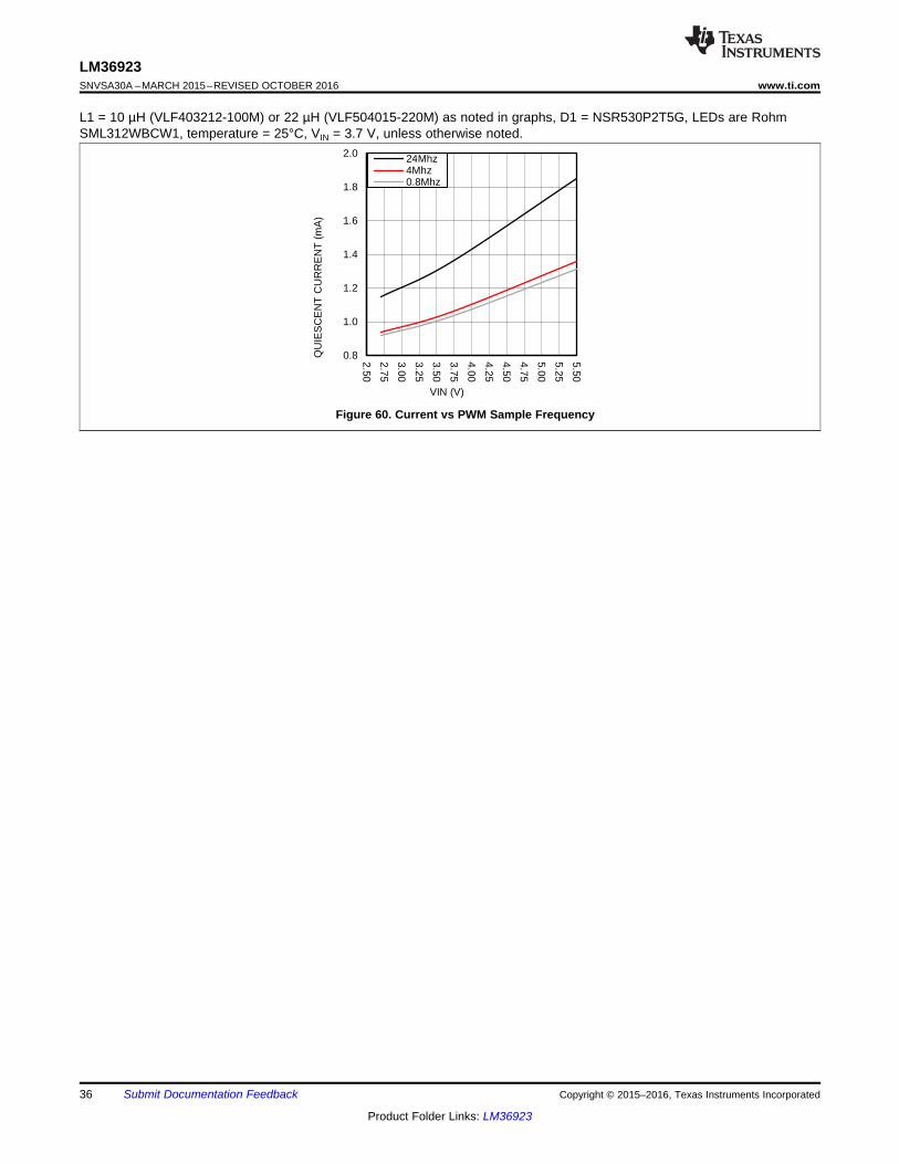
0.8
1.0
1.2
1.4
1.6
1.8
2.0
2.50
2.75
3.00
3.25
3.50
3.75
4.00
4.25
4.50
4.75
5.00
5.25
5.50Q
UIE
SC
EN
T C
UR
RE
NT
(m
A)
VIN (V)
24Mhz4Mhz0.8Mhz
C001
36
LM36923SNVSA30A –MARCH 2015–REVISED OCTOBER 2016 www.ti.com
Product Folder Links: LM36923
Submit Documentation Feedback Copyright © 2015–2016, Texas Instruments Incorporated
L1 = 10 µH (VLF403212-100M) or 22 µH (VLF504015-220M) as noted in graphs, D1 = NSR530P2T5G, LEDs are RohmSML312WBCW1, temperature = 25°C, VIN = 3.7 V, unless otherwise noted.
Figure 60. Current vs PWM Sample Frequency
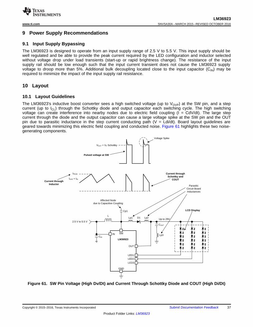
SWIN
OUT
LED1
GND
LM36923
2.5 V to 5.5 VUp to 29V
LD1Lp1 Lp2
Lp3
Cp1
Affected Nodedue to Capacitive Coupling
Current through Inductor
Pulsed voltage at SW
VOUT + VF Schottky
Voltage Spike
IPEAK
IAVE = IIN
Current through Schottky and
COUT
LCD Display
LED2
COUT
CIN
LED3
Parasitic Circuit Board Inductances
37
LM36923www.ti.com SNVSA30A –MARCH 2015–REVISED OCTOBER 2016
Product Folder Links: LM36923
Submit Documentation FeedbackCopyright © 2015–2016, Texas Instruments Incorporated
9 Power Supply Recommendations
9.1 Input Supply BypassingThe LM36923 is designed to operate from an input supply range of 2.5 V to 5.5 V. This input supply should bewell regulated and be able to provide the peak current required by the LED configuration and inductor selectedwithout voltage drop under load transients (start-up or rapid brightness change). The resistance of the inputsupply rail should be low enough such that the input current transient does not cause the LM36923 supplyvoltage to droop more than 5%. Additional bulk decoupling located close to the input capacitor (CIN) may berequired to minimize the impact of the input supply rail resistance.
10 Layout
10.1 Layout GuidelinesThe LM36923's inductive boost converter sees a high switched voltage (up to VOVP) at the SW pin, and a stepcurrent (up to ICL) through the Schottky diode and output capacitor each switching cycle. The high switchingvoltage can create interference into nearby nodes due to electric field coupling (I = CdV/dt). The large stepcurrent through the diode and the output capacitor can cause a large voltage spike at the SW pin and the OUTpin due to parasitic inductance in the step current conducting path (V = Ldi/dt). Board layout guidelines aregeared towards minimizing this electric field coupling and conducted noise. Figure 61 highlights these two noise-generating components.
Figure 61. SW Pin Voltage (High Dv/Dt) and Current Through Schottky Diode and COUT (High Di/Dt)
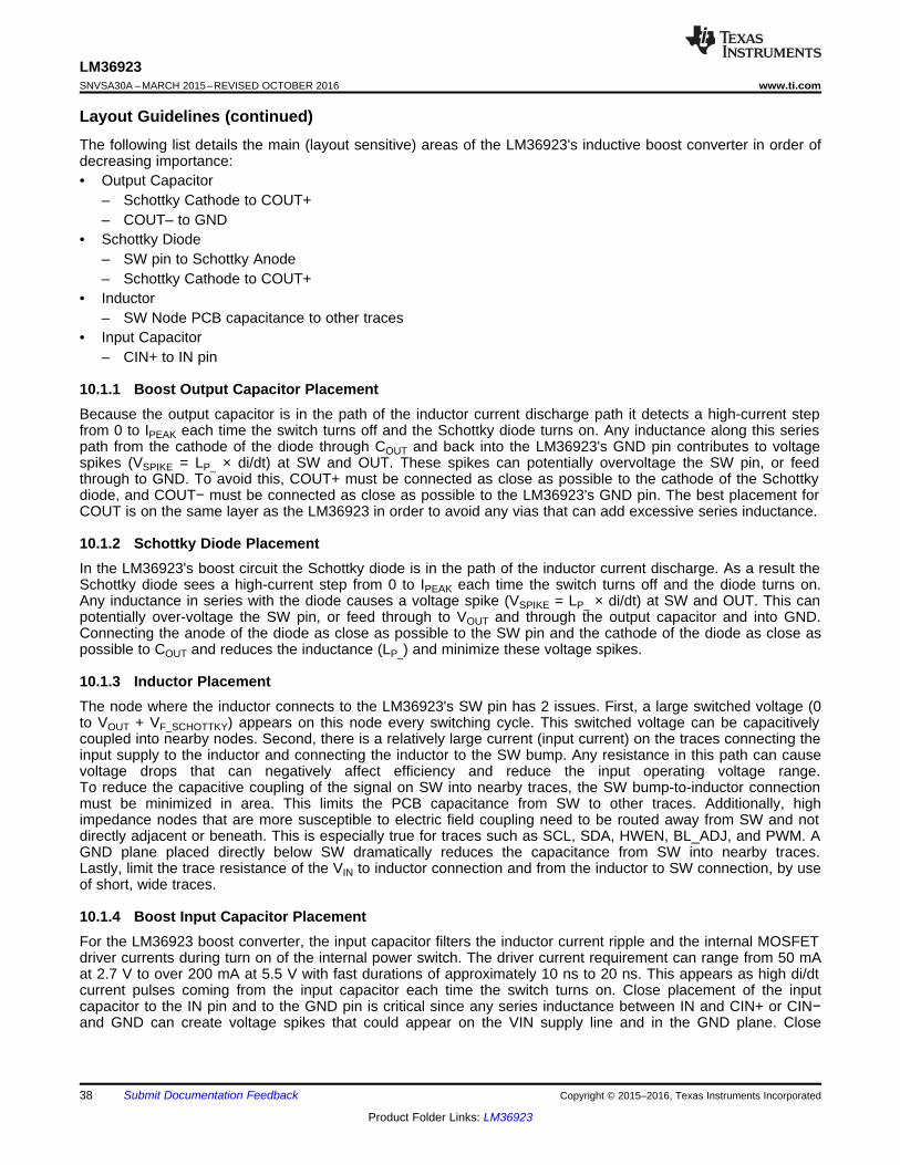
38
LM36923SNVSA30A –MARCH 2015–REVISED OCTOBER 2016 www.ti.com
Product Folder Links: LM36923
Submit Documentation Feedback Copyright © 2015–2016, Texas Instruments Incorporated
Layout Guidelines (continued)The following list details the main (layout sensitive) areas of the LM36923's inductive boost converter in order ofdecreasing importance:• Output Capacitor
– Schottky Cathode to COUT+– COUT– to GND
• Schottky Diode– SW pin to Schottky Anode– Schottky Cathode to COUT+
• Inductor– SW Node PCB capacitance to other traces
• Input Capacitor– CIN+ to IN pin
10.1.1 Boost Output Capacitor PlacementBecause the output capacitor is in the path of the inductor current discharge path it detects a high-current stepfrom 0 to IPEAK each time the switch turns off and the Schottky diode turns on. Any inductance along this seriespath from the cathode of the diode through COUT and back into the LM36923's GND pin contributes to voltagespikes (VSPIKE = LP_ × di/dt) at SW and OUT. These spikes can potentially overvoltage the SW pin, or feedthrough to GND. To avoid this, COUT+ must be connected as close as possible to the cathode of the Schottkydiode, and COUT− must be connected as close as possible to the LM36923's GND pin. The best placement forCOUT is on the same layer as the LM36923 in order to avoid any vias that can add excessive series inductance.
10.1.2 Schottky Diode PlacementIn the LM36923's boost circuit the Schottky diode is in the path of the inductor current discharge. As a result theSchottky diode sees a high-current step from 0 to IPEAK each time the switch turns off and the diode turns on.Any inductance in series with the diode causes a voltage spike (VSPIKE = LP_ × di/dt) at SW and OUT. This canpotentially over-voltage the SW pin, or feed through to VOUT and through the output capacitor and into GND.Connecting the anode of the diode as close as possible to the SW pin and the cathode of the diode as close aspossible to COUT and reduces the inductance (LP_) and minimize these voltage spikes.
10.1.3 Inductor PlacementThe node where the inductor connects to the LM36923's SW pin has 2 issues. First, a large switched voltage (0to VOUT + VF_SCHOTTKY) appears on this node every switching cycle. This switched voltage can be capacitivelycoupled into nearby nodes. Second, there is a relatively large current (input current) on the traces connecting theinput supply to the inductor and connecting the inductor to the SW bump. Any resistance in this path can causevoltage drops that can negatively affect efficiency and reduce the input operating voltage range.To reduce the capacitive coupling of the signal on SW into nearby traces, the SW bump-to-inductor connectionmust be minimized in area. This limits the PCB capacitance from SW to other traces. Additionally, highimpedance nodes that are more susceptible to electric field coupling need to be routed away from SW and notdirectly adjacent or beneath. This is especially true for traces such as SCL, SDA, HWEN, BL_ADJ, and PWM. AGND plane placed directly below SW dramatically reduces the capacitance from SW into nearby traces.Lastly, limit the trace resistance of the VIN to inductor connection and from the inductor to SW connection, by useof short, wide traces.
10.1.4 Boost Input Capacitor PlacementFor the LM36923 boost converter, the input capacitor filters the inductor current ripple and the internal MOSFETdriver currents during turn on of the internal power switch. The driver current requirement can range from 50 mAat 2.7 V to over 200 mA at 5.5 V with fast durations of approximately 10 ns to 20 ns. This appears as high di/dtcurrent pulses coming from the input capacitor each time the switch turns on. Close placement of the inputcapacitor to the IN pin and to the GND pin is critical since any series inductance between IN and CIN+ or CIN−and GND can create voltage spikes that could appear on the VIN supply line and in the GND plane. Close
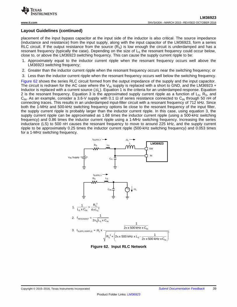
1.
2
S2
S LkHz5002R -xxS+
LSL
RS
CIN
LM36923
-+
VIN Supply
ISUPPLY 'IL
SW
LS
CIN
RS
ISUPPLY
'IL
2.
3.
1>
2SR
2SL4 xINS CL x
1RESONANTf =
2S INS CL x
xLI'|LESUPPLYRIPPI
¸¸¹
·¨¨©
§ 1
INCkHz5002 xxS
1
INCkHz5002 xxS
IN
39
LM36923www.ti.com SNVSA30A –MARCH 2015–REVISED OCTOBER 2016
Product Folder Links: LM36923
Submit Documentation FeedbackCopyright © 2015–2016, Texas Instruments Incorporated
Layout Guidelines (continued)placement of the input bypass capacitor at the input side of the inductor is also critical. The source impedance(inductance and resistance) from the input supply, along with the input capacitor of the LM36923, form a seriesRLC circuit. If the output resistance from the source (RS) is low enough the circuit is underdamped and has aresonant frequency (typically the case). Depending on the size of LS the resonant frequency could occur below,close to, or above the LM36923 switching frequency. This can cause the supply current ripple to be:1. Approximately equal to the inductor current ripple when the resonant frequency occurs well above the
LM36923 switching frequency;2. Greater than the inductor current ripple when the resonant frequency occurs near the switching frequency; or3. Less than the inductor current ripple when the resonant frequency occurs well below the switching frequency.
Figure 62 shows the series RLC circuit formed from the output impedance of the supply and the input capacitor.The circuit is redrawn for the AC case where the VIN supply is replaced with a short to GND, and the LM36923 +Inductor is replaced with a current source (ΔIL). Equation 1 is the criteria for an underdamped response. Equation2 is the resonant frequency. Equation 3 is the approximated supply current ripple as a function of LS, RS, andCIN. As an example, consider a 3.6-V supply with 0.1 Ω of series resistance connected to CIN through 50 nH ofconnecting traces. This results in an underdamped input-filter circuit with a resonant frequency of 712 kHz. Sinceboth the 1-MHz and 500-kHz switching frequency options lie close to the resonant frequency of the input filter,the supply current ripple is probably larger than the inductor current ripple. In this case, using equation 3, thesupply current ripple can be approximated as 1.68 times the inductor current ripple (using a 500-kHz switchingfrequency) and 0.86 times the inductor current ripple using a 1-MHz switching frequency. Increasing the seriesinductance (LS) to 500 nH causes the resonant frequency to move to around 225 kHz, and the supply currentripple to be approximately 0.25 times the inductor current ripple (500-kHz switching frequency) and 0.053 timesfor a 1-MHz switching frequency.
Figure 62. Input RLC Network
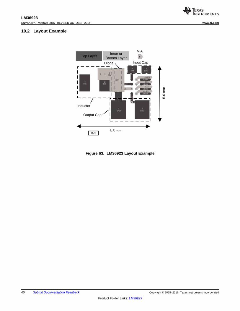
6.5 mm
5.0
mm
Output Cap
Diode Input Cap
Inductor
BLADJ
Top LayerInner or
Bottom Layer
VIA
OUT
40
LM36923SNVSA30A –MARCH 2015–REVISED OCTOBER 2016 www.ti.com
Product Folder Links: LM36923
Submit Documentation Feedback Copyright © 2015–2016, Texas Instruments Incorporated
10.2 Layout Example
Figure 63. LM36923 Layout Example

41
LM36923www.ti.com SNVSA30A –MARCH 2015–REVISED OCTOBER 2016
Product Folder Links: LM36923
Submit Documentation FeedbackCopyright © 2015–2016, Texas Instruments Incorporated
11 Device and Documentation Support
11.1 Device Support
11.1.1 Third-Party Products DisclaimerTI'S PUBLICATION OF INFORMATION REGARDING THIRD-PARTY PRODUCTS OR SERVICES DOES NOTCONSTITUTE AN ENDORSEMENT REGARDING THE SUITABILITY OF SUCH PRODUCTS OR SERVICESOR A WARRANTY, REPRESENTATION OR ENDORSEMENT OF SUCH PRODUCTS OR SERVICES, EITHERALONE OR IN COMBINATION WITH ANY TI PRODUCT OR SERVICE.
11.2 Receiving Notification of Documentation UpdatesTo receive notification of documentation updates, navigate to the device product folder on ti.com. In the upperright corner, click on Alert me to register and receive a weekly digest of any product information that haschanged. For change details, review the revision history included in any revised document.
11.3 Community ResourcesThe following links connect to TI community resources. Linked contents are provided "AS IS" by the respectivecontributors. They do not constitute TI specifications and do not necessarily reflect TI's views; see TI's Terms ofUse.
TI E2E™ Online Community TI's Engineer-to-Engineer (E2E) Community. Created to foster collaborationamong engineers. At e2e.ti.com, you can ask questions, share knowledge, explore ideas and helpsolve problems with fellow engineers.
Design Support TI's Design Support Quickly find helpful E2E forums along with design support tools andcontact information for technical support.
11.4 TrademarksE2E is a trademark of Texas Instruments.All other trademarks are the property of their respective owners.
11.5 Electrostatic Discharge CautionThis integrated circuit can be damaged by ESD. Texas Instruments recommends that all integrated circuits be handled withappropriate precautions. Failure to observe proper handling and installation procedures can cause damage.
ESD damage can range from subtle performance degradation to complete device failure. Precision integrated circuits may be moresusceptible to damage because very small parametric changes could cause the device not to meet its published specifications.
11.6 GlossarySLYZ022 — TI Glossary.
This glossary lists and explains terms, acronyms, and definitions.
12 Mechanical, Packaging, and Orderable InformationThe following pages include mechanical, packaging, and orderable information. This information is the mostcurrent data available for the designated devices. This data is subject to change without notice and revision ofthis document. For browser-based versions of this data sheet, refer to the left-hand navigation.
PACKAGE OPTION ADDENDUM
www.ti.com 10-Dec-2020
Addendum-Page 1
PACKAGING INFORMATION
Orderable Device Status(1)
Package Type PackageDrawing
Pins PackageQty
Eco Plan(2)
Lead finish/Ball material
(6)
MSL Peak Temp(3)
Op Temp (°C) Device Marking(4/5)
Samples
LM36923YFFR ACTIVE DSBGA YFF 12 3000 RoHS & Green SNAGCU Level-1-260C-UNLIM -40 to 85 36923
(1) The marketing status values are defined as follows:ACTIVE: Product device recommended for new designs.LIFEBUY: TI has announced that the device will be discontinued, and a lifetime-buy period is in effect.NRND: Not recommended for new designs. Device is in production to support existing customers, but TI does not recommend using this part in a new design.PREVIEW: Device has been announced but is not in production. Samples may or may not be available.OBSOLETE: TI has discontinued the production of the device.
(2) RoHS: TI defines "RoHS" to mean semiconductor products that are compliant with the current EU RoHS requirements for all 10 RoHS substances, including the requirement that RoHS substancedo not exceed 0.1% by weight in homogeneous materials. Where designed to be soldered at high temperatures, "RoHS" products are suitable for use in specified lead-free processes. TI mayreference these types of products as "Pb-Free".RoHS Exempt: TI defines "RoHS Exempt" to mean products that contain lead but are compliant with EU RoHS pursuant to a specific EU RoHS exemption.Green: TI defines "Green" to mean the content of Chlorine (Cl) and Bromine (Br) based flame retardants meet JS709B low halogen requirements of <=1000ppm threshold. Antimony trioxide basedflame retardants must also meet the <=1000ppm threshold requirement.
(3) MSL, Peak Temp. - The Moisture Sensitivity Level rating according to the JEDEC industry standard classifications, and peak solder temperature.
(4) There may be additional marking, which relates to the logo, the lot trace code information, or the environmental category on the device.
(5) Multiple Device Markings will be inside parentheses. Only one Device Marking contained in parentheses and separated by a "~" will appear on a device. If a line is indented then it is a continuationof the previous line and the two combined represent the entire Device Marking for that device.
(6) Lead finish/Ball material - Orderable Devices may have multiple material finish options. Finish options are separated by a vertical ruled line. Lead finish/Ball material values may wrap to twolines if the finish value exceeds the maximum column width.
Important Information and Disclaimer:The information provided on this page represents TI's knowledge and belief as of the date that it is provided. TI bases its knowledge and belief on informationprovided by third parties, and makes no representation or warranty as to the accuracy of such information. Efforts are underway to better integrate information from third parties. TI has taken andcontinues to take reasonable steps to provide representative and accurate information but may not have conducted destructive testing or chemical analysis on incoming materials and chemicals.TI and TI suppliers consider certain information to be proprietary, and thus CAS numbers and other limited information may not be available for release.
In no event shall TI's liability arising out of such information exceed the total purchase price of the TI part(s) at issue in this document sold by TI to Customer on an annual basis.
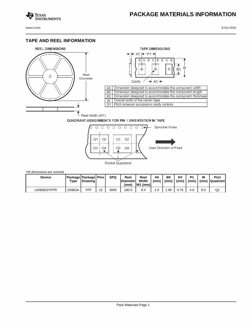
TAPE AND REEL INFORMATION
*All dimensions are nominal
Device PackageType
PackageDrawing
Pins SPQ ReelDiameter
(mm)
ReelWidth
W1 (mm)
A0(mm)
B0(mm)
K0(mm)
P1(mm)
W(mm)
Pin1Quadrant
LM36923YFFR DSBGA YFF 12 3000 180.0 8.4 1.5 1.99 0.75 4.0 8.0 Q1
PACKAGE MATERIALS INFORMATION
www.ti.com 8-Oct-2016
Pack Materials-Page 1

*All dimensions are nominal
Device Package Type Package Drawing Pins SPQ Length (mm) Width (mm) Height (mm)
LM36923YFFR DSBGA YFF 12 3000 182.0 182.0 20.0
PACKAGE MATERIALS INFORMATION
www.ti.com 8-Oct-2016
Pack Materials-Page 2
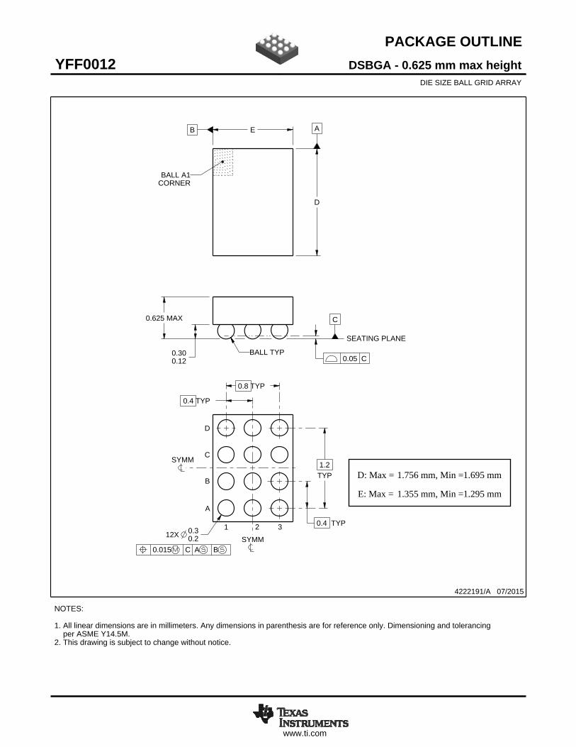
www.ti.com
PACKAGE OUTLINE
C0.625 MAX
0.300.12
1.2TYP
0.8 TYP
0.4 TYP
0.4 TYP
12X 0.30.2
B E A
D
DSBGA - 0.625 mm max heightYFF0012DIE SIZE BALL GRID ARRAY
4222191/A 07/2015
NOTES: 1. All linear dimensions are in millimeters. Any dimensions in parenthesis are for reference only. Dimensioning and tolerancing per ASME Y14.5M.2. This drawing is subject to change without notice.
BALL A1CORNER
SEATING PLANE
BALL TYP0.05 C
B
1 2 3
0.015 C A B
SYMM
SYMM
A
C
D
SCALE 8.000
D: Max =
E: Max =
1.756 mm, Min =
1.355 mm, Min =
1.695 mm
1.295 mm
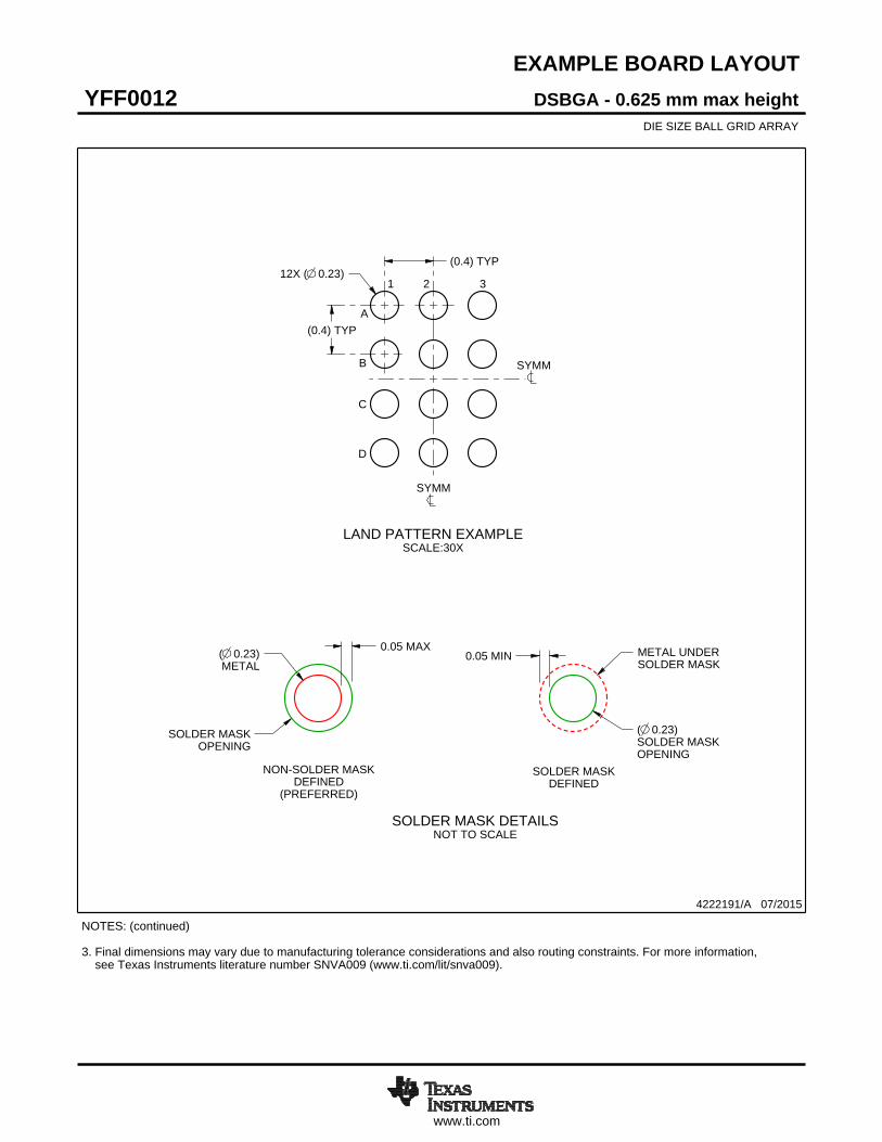
www.ti.com
EXAMPLE BOARD LAYOUT
12X ( )0.23(0.4) TYP
(0.4) TYP
( )METAL
0.23 0.05 MAX
SOLDER MASKOPENING
METAL UNDERSOLDER MASK
( )SOLDER MASKOPENING
0.23
0.05 MIN
DSBGA - 0.625 mm max heightYFF0012DIE SIZE BALL GRID ARRAY
4222191/A 07/2015
NOTES: (continued) 3. Final dimensions may vary due to manufacturing tolerance considerations and also routing constraints. For more information, see Texas Instruments literature number SNVA009 (www.ti.com/lit/snva009).
SYMM
SYMM
LAND PATTERN EXAMPLESCALE:30X
C
1 2 3
A
B
D
NON-SOLDER MASKDEFINED
(PREFERRED)
SOLDER MASK DETAILSNOT TO SCALE
SOLDER MASKDEFINED
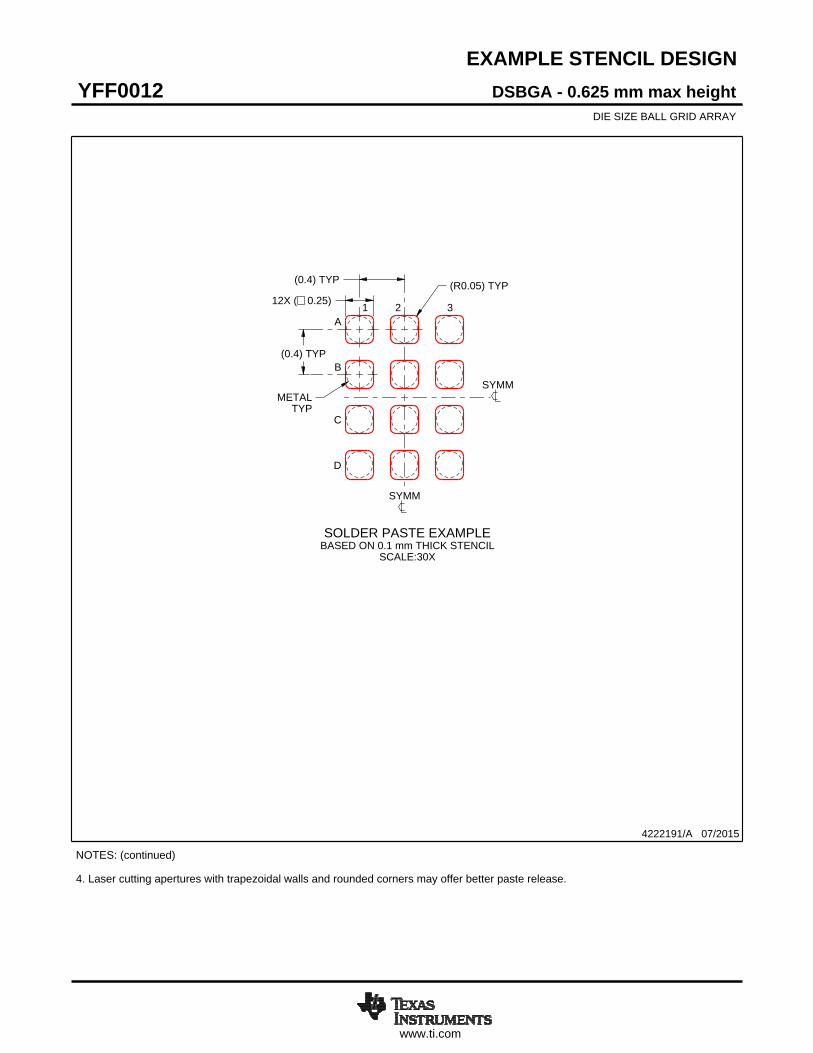
www.ti.com
EXAMPLE STENCIL DESIGN
(0.4) TYP
(0.4) TYP
12X ( 0.25)(R ) TYP0.05
METALTYP
DSBGA - 0.625 mm max heightYFF0012DIE SIZE BALL GRID ARRAY
4222191/A 07/2015
NOTES: (continued) 4. Laser cutting apertures with trapezoidal walls and rounded corners may offer better paste release.
SYMM
SYMM
C
1 2 3A
B
D
SOLDER PASTE EXAMPLEBASED ON 0.1 mm THICK STENCIL
SCALE:30X

IMPORTANT NOTICE AND DISCLAIMER
TI PROVIDES TECHNICAL AND RELIABILITY DATA (INCLUDING DATASHEETS), DESIGN RESOURCES (INCLUDING REFERENCE DESIGNS), APPLICATION OR OTHER DESIGN ADVICE, WEB TOOLS, SAFETY INFORMATION, AND OTHER RESOURCES “AS IS” AND WITH ALL FAULTS, AND DISCLAIMS ALL WARRANTIES, EXPRESS AND IMPLIED, INCLUDING WITHOUT LIMITATION ANY IMPLIED WARRANTIES OF MERCHANTABILITY, FITNESS FOR A PARTICULAR PURPOSE OR NON-INFRINGEMENT OF THIRD PARTY INTELLECTUAL PROPERTY RIGHTS.These resources are intended for skilled developers designing with TI products. You are solely responsible for (1) selecting the appropriate TI products for your application, (2) designing, validating and testing your application, and (3) ensuring your application meets applicable standards, and any other safety, security, or other requirements. These resources are subject to change without notice. TI grants you permission to use these resources only for development of an application that uses the TI products described in the resource. Other reproduction and display of these resources is prohibited. No license is granted to any other TI intellectual property right or to any third party intellectual property right. TI disclaims responsibility for, and you will fully indemnify TI and its representatives against, any claims, damages, costs, losses, and liabilities arising out of your use of these resources.TI’s products are provided subject to TI’s Terms of Sale (www.ti.com/legal/termsofsale.html) or other applicable terms available either on ti.com or provided in conjunction with such TI products. TI’s provision of these resources does not expand or otherwise alter TI’s applicable warranties or warranty disclaimers for TI products.
Mailing Address: Texas Instruments, Post Office Box 655303, Dallas, Texas 75265Copyright © 2020, Texas Instruments Incorporated
Related Documents


![[MS-ODBCSTR]: ODBC Connection String Structure Specification · driver-specific key: A keyword in a connection string that is interpreted by an individual driver. Drivers can have](https://static.cupdf.com/doc/110x72/5f88c3e21fde883c7310c18b/ms-odbcstr-odbc-connection-string-structure-specification-driver-specific-key.jpg)