IN OUT SW TX/TORCH SDA SCL 1 2H 10 2F 10 2F STROBE LED Flash LED 2.5V to 5.5V GND Product Folder Sample & Buy Technical Documents Tools & Software Support & Community LM3642 SNVS891H – SEPTEMBER 2012 – REVISED SEPTEMBER 2015 LM3642 1.5-A Synchronous Boost LED Flash Driver With High-Side Current Source 1 Features 3 Description The LM3642 is a 4-MHz fixed-frequency synchronous 1• 1.5-A High-Side Current Source for Single LED boost converter plus 1.5-A constant current driver for • > 85% Efficiency in Torch Mode (at 100 mA) and a high-current white LED. The high-side current Flash Mode (at 1 A to 1.5 A) source allows for grounded cathode LED operation • Accurate Programmable Flash LED Current from providing Flash current up to 1.5 A. An adaptive regulation method ensures the current source 93 mA to 1.5 A remains in regulation and maximizes efficiency. • Accurate Programmable Torch LED Currents: The LM3642 is controlled via an I 2 C-compatible – 48.4 mA to 375 mA interface. Features include a hardware flash enable – 24 mA to 187 mA (LT option) (STROBE) allowing a logic input to trigger the flash • Small Solution Size: < 20 mm 2 pulse as well as a TX input which forces the flash • Soft-Start Operation for Battery Protection pulse into a low-current Torch Mode, allowing for synchronization to RF power amplifier events or other • Hardware Strobe Enable high-current conditions. • Synchronization Input for RF Power Amplifier The 4-MHz switching frequency, overvoltage Pulse Events protection and adjustable current limit settings allow • V IN Flash Monitor Optimization the use of tiny, low-profile inductors and (10-μF) • 400-kHz I 2 C-Compatible Interface ceramic capacitors. The device is available in a small • 0.5-mm Pitch, 9-Bump DSBGA 9-bump DSBGA package and operates over the −40°C to 85°C temperature range. 2 Applications Device Information (1) Camera Phone LED Flash PART NUMBER PACKAGE BODY SIZE (MAX) LM3642 DSBGA (9) 1.69 mm × 1.64 mm (1) For all available packages, see the orderable addendum at the end of the data sheet. Simplified Schematic 1 An IMPORTANT NOTICE at the end of this data sheet addresses availability, warranty, changes, use in safety-critical applications, intellectual property matters and other important disclaimers. PRODUCTION DATA.

Welcome message from author
This document is posted to help you gain knowledge. Please leave a comment to let me know what you think about it! Share it to your friends and learn new things together.
Transcript
IN OUTSW
TX/TORCHSDASCL
1 PH
10 PF 10 PF
STROBE LED
Flash LED
2.5V to 5.5V
GND
Product
Folder
Sample &Buy
Technical
Documents
Tools &
Software
Support &Community
LM3642SNVS891H –SEPTEMBER 2012–REVISED SEPTEMBER 2015
LM3642 1.5-A Synchronous Boost LED Flash Driver With High-Side Current Source1 Features 3 Description
The LM3642 is a 4-MHz fixed-frequency synchronous1• 1.5-A High-Side Current Source for Single LED
boost converter plus 1.5-A constant current driver for• > 85% Efficiency in Torch Mode (at 100 mA) and a high-current white LED. The high-side currentFlash Mode (at 1 A to 1.5 A) source allows for grounded cathode LED operation
• Accurate Programmable Flash LED Current from providing Flash current up to 1.5 A. An adaptiveregulation method ensures the current source93 mA to 1.5 Aremains in regulation and maximizes efficiency.• Accurate Programmable Torch LED Currents:The LM3642 is controlled via an I2C-compatible– 48.4 mA to 375 mAinterface. Features include a hardware flash enable– 24 mA to 187 mA (LT option) (STROBE) allowing a logic input to trigger the flash
• Small Solution Size: < 20 mm2pulse as well as a TX input which forces the flash
• Soft-Start Operation for Battery Protection pulse into a low-current Torch Mode, allowing forsynchronization to RF power amplifier events or other• Hardware Strobe Enablehigh-current conditions.• Synchronization Input for RF Power AmplifierThe 4-MHz switching frequency, overvoltagePulse Eventsprotection and adjustable current limit settings allow• VIN Flash Monitor Optimization the use of tiny, low-profile inductors and (10-µF)
• 400-kHz I2C-Compatible Interface ceramic capacitors. The device is available in a small• 0.5-mm Pitch, 9-Bump DSBGA 9-bump DSBGA package and operates over the
−40°C to 85°C temperature range.2 Applications
Device Information(1)Camera Phone LED Flash
PART NUMBER PACKAGE BODY SIZE (MAX)LM3642 DSBGA (9) 1.69 mm × 1.64 mm
(1) For all available packages, see the orderable addendum atthe end of the data sheet.
Simplified Schematic
1
An IMPORTANT NOTICE at the end of this data sheet addresses availability, warranty, changes, use in safety-critical applications,intellectual property matters and other important disclaimers. PRODUCTION DATA.
LM3642SNVS891H –SEPTEMBER 2012–REVISED SEPTEMBER 2015 www.ti.com
Table of Contents7.5 Programming........................................................... 121 Features .................................................................. 17.6 Register Map........................................................... 152 Applications ........................................................... 1
8 Application and Implementation ........................ 183 Description ............................................................. 18.1 Application Information............................................ 184 Revision History..................................................... 28.2 Typical Application ................................................. 185 Pin Configuration and Functions ......................... 3
9 Power Supply Recommendations ...................... 226 Specifications......................................................... 410 Layout................................................................... 226.1 Absolute Maximum Ratings ...................................... 4
10.1 Layout Guidelines ................................................. 226.2 ESD Ratings.............................................................. 410.2 Layout Example .................................................... 236.3 Recommended Operating Conditions....................... 4
11 Device and Documentation Support ................. 246.4 Thermal Information .................................................. 411.1 Device Support...................................................... 246.5 Electrical Characteristics........................................... 511.2 Documentation Support ........................................ 246.6 Timing Requirements ................................................ 611.3 Trademarks ........................................................... 246.7 Typical Characteristics .............................................. 711.4 Community Resources.......................................... 247 Detailed Description .............................................. 911.5 Electrostatic Discharge Caution............................ 247.1 Overview ................................................................... 911.6 Glossary ................................................................ 247.2 Functional Block Diagram ......................................... 9
12 Mechanical, Packaging, and Orderable7.3 Feature Description................................................. 10Information ........................................................... 247.4 Device Functional Modes........................................ 11
4 Revision HistoryNOTE: Page numbers for previous revisions may differ from page numbers in the current version.
Changes from Revision G (December 2014) to Revision H Page
• Changed Handling Ratings table to ESD Ratings table per SDS format; move Storage Temp to Abs Max table ............... 4• Added "If an I2C command is used to terminate the flash event, TI recommends selecting a flash time-out level 100
ms above the desired flash duration ." to end of Flash Time-Out subsection...................................................................... 10
Changes from Revision F (December 2013) to Revision G Page
• Added Pin Configuration and Functions section, Handling Rating table, Feature Description section, DeviceFunctional Modes, Application and Implementation section, Power Supply Recommendations section, Layoutsection, Device and Documentation Support section, and Mechanical, Packaging, and Orderable Informationsection ................................................................................................................................................................................... 1
• Added updated full Thermal Information ............................................................................................................................... 4
Changes from Revision E (May 2013) to Revision F Page
• Deleted TX interrupt ............................................................................................................................................................... 9
2 Submit Documentation Feedback Copyright © 2012–2015, Texas Instruments Incorporated
Product Folder Links: LM3642
A1 A2
B1 B2 B3
Top View
A3
C2C1 C3
LM3642www.ti.com SNVS891H –SEPTEMBER 2012–REVISED SEPTEMBER 2015
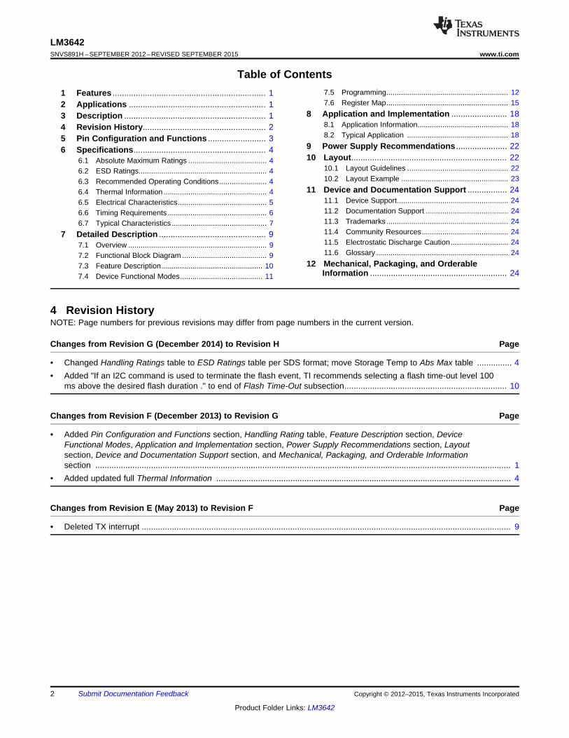
5 Pin Configuration and Functions
YZR Package9-Pin DSBGA
Top View
Pin FunctionsPIN
I/O DESCRIPTIONNO. NAME
Step-up DC-DC converter output. Connect a 10-µF ceramic capacitor between this pinA1 OUT Power and GND.A2 SW Power Drain connection for internal NMOS and synchronous PMOS switches.A3 GND Ground GroundB1 LED Output High-side current source output for Flash LED.
Active high hardware Flash enable. Drive STROBE high to turn on Flash pulse. Has anB2 STROBE Input internal pulldown resistor of 300 kΩ between STROBE and GND.Input voltage connection. Connect IN to the input supply, and bypass to GND with a 10-B3 IN Power µF or larger ceramic capacitor.Configurable power amplifier synchronization input or configurable active high TorchC1 TX/TORCH Input enable. Has an internal pulldown resistor of 300 kΩ between TX and GND.
C2 SDA Input/Output Serial data input/output.C3 SCL Input Serial clock input.
Copyright © 2012–2015, Texas Instruments Incorporated Submit Documentation Feedback 3
Product Folder Links: LM3642
LM3642SNVS891H –SEPTEMBER 2012–REVISED SEPTEMBER 2015 www.ti.com
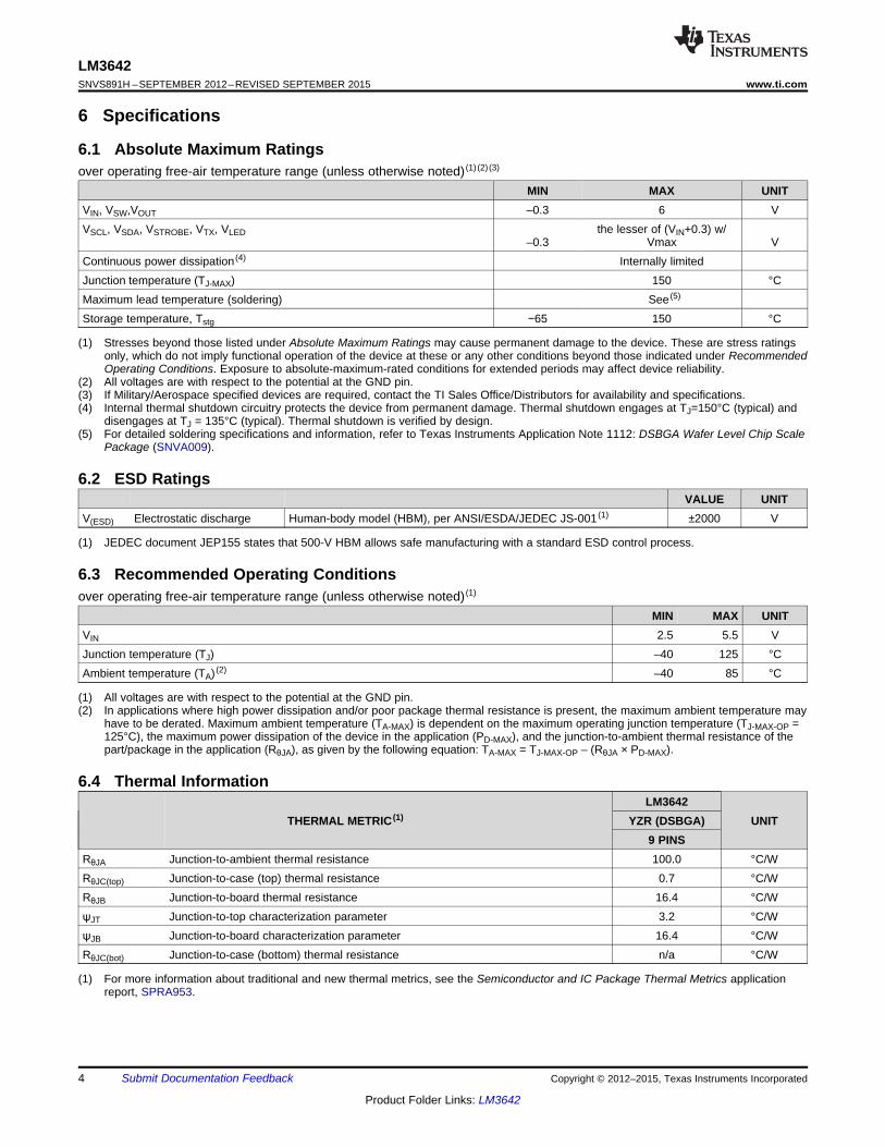
6 Specifications
6.1 Absolute Maximum Ratingsover operating free-air temperature range (unless otherwise noted) (1) (2) (3)
MIN MAX UNITVIN, VSW,VOUT –0.3 6 VVSCL, VSDA, VSTROBE, VTX, VLED the lesser of (VIN+0.3) w/
–0.3 Vmax VContinuous power dissipation (4) Internally limitedJunction temperature (TJ-MAX) 150 °CMaximum lead temperature (soldering) See (5)
Storage temperature, Tstg −65 150 °C
(1) Stresses beyond those listed under Absolute Maximum Ratings may cause permanent damage to the device. These are stress ratingsonly, which do not imply functional operation of the device at these or any other conditions beyond those indicated under RecommendedOperating Conditions. Exposure to absolute-maximum-rated conditions for extended periods may affect device reliability.
(2) All voltages are with respect to the potential at the GND pin.(3) If Military/Aerospace specified devices are required, contact the TI Sales Office/Distributors for availability and specifications.(4) Internal thermal shutdown circuitry protects the device from permanent damage. Thermal shutdown engages at TJ=150°C (typical) and
disengages at TJ = 135°C (typical). Thermal shutdown is verified by design.(5) For detailed soldering specifications and information, refer to Texas Instruments Application Note 1112: DSBGA Wafer Level Chip Scale
Package (SNVA009).
6.2 ESD RatingsVALUE UNIT
V(ESD) Electrostatic discharge Human-body model (HBM), per ANSI/ESDA/JEDEC JS-001 (1) ±2000 V
(1) JEDEC document JEP155 states that 500-V HBM allows safe manufacturing with a standard ESD control process.
6.3 Recommended Operating Conditionsover operating free-air temperature range (unless otherwise noted) (1)
MIN MAX UNITVIN 2.5 5.5 VJunction temperature (TJ) –40 125 °CAmbient temperature (TA) (2) –40 85 °C
(1) All voltages are with respect to the potential at the GND pin.(2) In applications where high power dissipation and/or poor package thermal resistance is present, the maximum ambient temperature may
have to be derated. Maximum ambient temperature (TA-MAX) is dependent on the maximum operating junction temperature (TJ-MAX-OP =125°C), the maximum power dissipation of the device in the application (PD-MAX), and the junction-to-ambient thermal resistance of thepart/package in the application (RθJA), as given by the following equation: TA-MAX = TJ-MAX-OP – (RθJA × PD-MAX).
6.4 Thermal InformationLM3642
THERMAL METRIC (1) YZR (DSBGA) UNIT9 PINS
RθJA Junction-to-ambient thermal resistance 100.0 °C/WRθJC(top) Junction-to-case (top) thermal resistance 0.7 °C/WRθJB Junction-to-board thermal resistance 16.4 °C/WψJT Junction-to-top characterization parameter 3.2 °C/WψJB Junction-to-board characterization parameter 16.4 °C/WRθJC(bot) Junction-to-case (bottom) thermal resistance n/a °C/W
(1) For more information about traditional and new thermal metrics, see the Semiconductor and IC Package Thermal Metrics applicationreport, SPRA953.
4 Submit Documentation Feedback Copyright © 2012–2015, Texas Instruments Incorporated
Product Folder Links: LM3642
LM3642www.ti.com SNVS891H –SEPTEMBER 2012–REVISED SEPTEMBER 2015
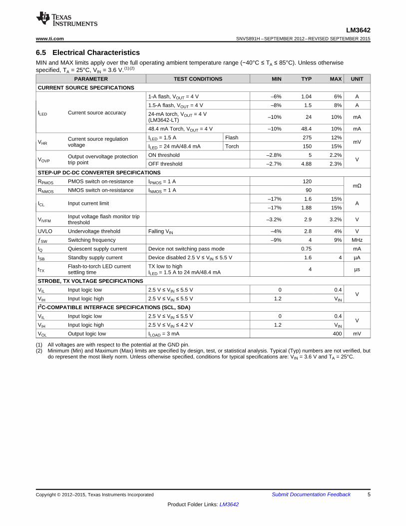
6.5 Electrical CharacteristicsMIN and MAX limits apply over the full operating ambient temperature range (−40°C ≤ TA ≤ 85°C). Unless otherwisespecified, TA = 25°C, VIN = 3.6 V. (1) (2)
PARAMETER TEST CONDITIONS MIN TYP MAX UNITCURRENT SOURCE SPECIFICATIONS
1-A flash, VOUT = 4 V –6% 1.04 6% A1.5-A flash, VOUT = 4 V –8% 1.5 8% A
ILED Current source accuracy 24-mA torch, VOUT = 4 V –10% 24 10% mA(LM3642-LT)48.4 mA Torch, VOUT = 4 V –10% 48.4 10% mAILED = 1.5 A Flash 275 12%Current source regulationVHR mVvoltage ILED = 24 mA/48.4 mA Torch 150 15%ON threshold –2.8% 5 2.2%Output overvoltage protectionVOVP Vtrip point OFF threshold –2.7% 4.88 2.3%
STEP-UP DC-DC CONVERTER SPECIFICATIONSRPMOS PMOS switch on-resistance IPMOS = 1 A 120
mΩRNMOS NMOS switch on-resistance INMOS = 1 A 90
–17% 1.6 15%ICL Input current limit A
–17% 1.88 15%Input voltage flash monitor tripVIVFM –3.2% 2.9 3.2% Vthreshold
UVLO Undervoltage threhold Falling VIN –4% 2.8 4% VƒSW Switching frequency –9% 4 9% MHzIQ Quiescent supply current Device not switching pass mode 0.75 mAISB Standby supply current Device disabled 2.5 V ≤ VIN ≤ 5.5 V 1.6 4 µA
Flash-to-torch LED current TX low to hightTX 4 µssettling time ILED = 1.5 A to 24 mA/48.4 mASTROBE, TX VOLTAGE SPECIFICATIONSVIL Input logic low 2.5 V ≤ VIN ≤ 5.5 V 0 0.4
VVIH Input logic high 2.5 V ≤ VIN ≤ 5.5 V 1.2 VIN
I2C-COMPATIBLE INTERFACE SPECIFICATIONS (SCL, SDA)VIL Input logic low 2.5 V ≤ VIN ≤ 5.5 V 0 0.4
VVIH Input logic high 2.5 V ≤ VIN ≤ 4.2 V 1.2 VIN
VOL Output logic low ILOAD = 3 mA 400 mV
(1) All voltages are with respect to the potential at the GND pin.(2) Minimum (Min) and Maximum (Max) limits are specified by design, test, or statistical analysis. Typical (Typ) numbers are not verified, but
do represent the most likely norm. Unless otherwise specified, conditions for typical specifications are: VIN = 3.6 V and TA = 25°C.
Copyright © 2012–2015, Texas Instruments Incorporated Submit Documentation Feedback 5
Product Folder Links: LM3642
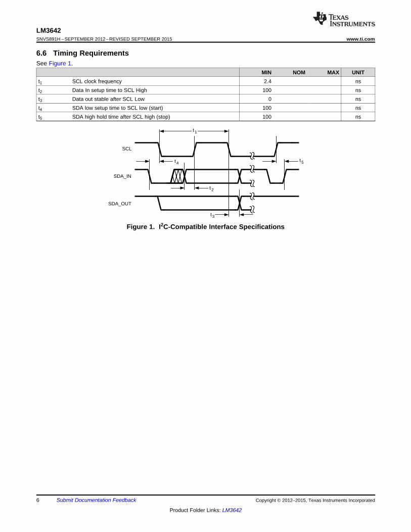
SCL
SDA_IN
SDA_OUT
t5
t1
t4
t3
t2
LM3642SNVS891H –SEPTEMBER 2012–REVISED SEPTEMBER 2015 www.ti.com
6.6 Timing RequirementsSee Figure 1.
MIN NOM MAX UNITt1 SCL clock frequency 2.4 nst2 Data In setup time to SCL High 100 nst3 Data out stable after SCL Low 0 nst4 SDA low setup time to SCL low (start) 100 nst5 SDA high hold time after SCL high (stop) 100 ns
Figure 1. I2C-Compatible Interface Specifications
6 Submit Documentation Feedback Copyright © 2012–2015, Texas Instruments Incorporated
Product Folder Links: LM3642
2.7 3.0 3.3 3.6 3.9 4.1 4.4 4.7 5.0 5.3 5.55.00
5.03
5.06
5.09
5.12
5.15
5.18
5.21
5.24
5.27
5.30
OU
TP
UT
VO
LTA
GE
(V
)
VIN (V)
+25°C+85°C-40°C
2.5 2.7 2.9 3.1 3.2 3.4 3.6 3.7 3.9 4.1 4.20.10
0.11
0.12
0.13
0.15
0.15
0.16
0.17
0.18
0.19
0.20
HE
AD
RO
OM
VO
LTA
GE
(V
)
VIN (V)
2.8 3.1 3.4 3.7 3.9 4.2 4.5 4.7 5.0 5.3 5.51.00
1.06
1.12
1.18
1.24
1.30
1.36
1.42
1.48
1.54
1.60
LED
CU
RR
EN
T (
A)
VIN (V)
1.5A
1.4A
1.31A
1.22A
1.1125A
2.8 3.0 3.1 3.3 3.4 3.5 3.7 3.8 4.0 4.1 4.20.15
0.18
0.20
0.23
0.25
0.28
0.30
0.33
0.35
0.38
0.40
HE
AD
RO
OM
VO
LTA
GE
(V
)
VIN (V)
+25°C+85°C-40°C
2.5 2.7 2.9 3.1 3.2 3.4 3.6 3.7 3.9 4.1 4.21.00
1.05
1.10
1.15
1.20
1.25
1.30
1.35
1.40
1.45
1.50LE
D C
UR
RE
NT
(A
)
VIN (V)
+25°C+85°C- 40°C
2.8 3.0 3.2 3.4 3.5 3.7 3.9 4.0 4.2 4.4 4.5
0.330
0.337
0.344
0.351
0.358
0.365
0.372
0.379
0.386
0.393
0.400
LED
CU
UR
EN
T (
A)
VIN(V)
+25°C+85°C-40°C
LM3642www.ti.com SNVS891H –SEPTEMBER 2012–REVISED SEPTEMBER 2015
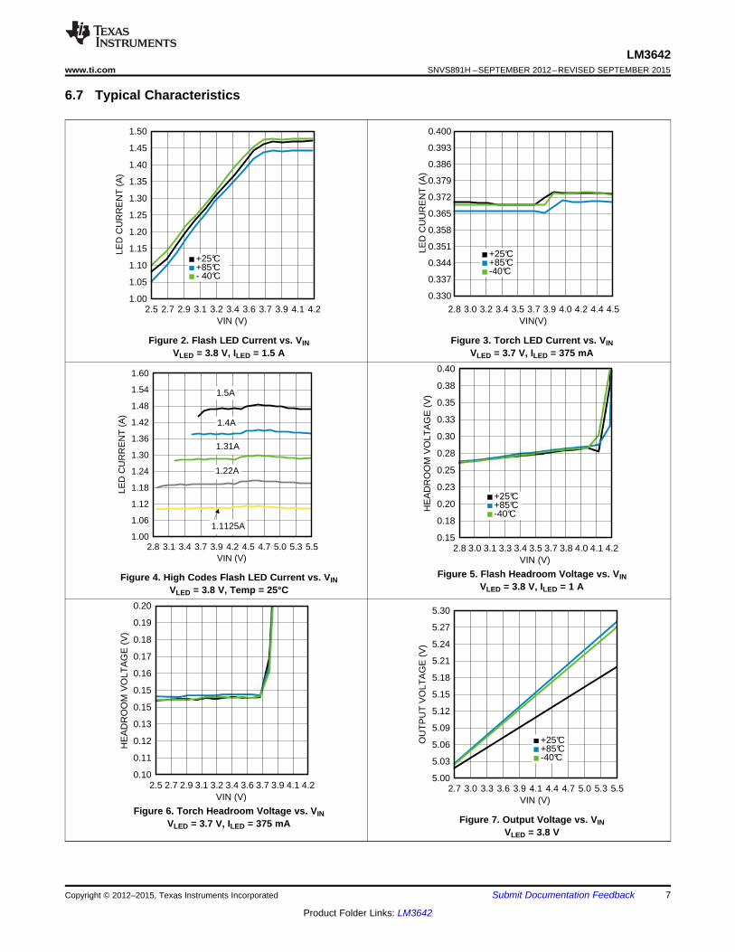
6.7 Typical Characteristics
Figure 2. Flash LED Current vs. VIN Figure 3. Torch LED Current vs. VINVLED = 3.8 V, ILED = 1.5 A VLED = 3.7 V, ILED = 375 mA
Figure 5. Flash Headroom Voltage vs. VINFigure 4. High Codes Flash LED Current vs. VINVLED = 3.8 V, ILED = 1 AVLED = 3.8 V, Temp = 25°C
Figure 6. Torch Headroom Voltage vs. VINFigure 7. Output Voltage vs. VINVLED = 3.7 V, ILED = 375 mA
VLED = 3.8 V
Copyright © 2012–2015, Texas Instruments Incorporated Submit Documentation Feedback 7
Product Folder Links: LM3642
2.8 3.0 3.1 3.3 3.4 3.5 3.7 3.8 4.0 4.1 4.21.50
1.55
1.60
1.65
1.70
1.75
1.80
1.85
1.90
1.95
2.00
AV
ER
AG
E IN
PU
T C
UR
RE
NT
(A
)
VIN (V)
+25°C+85°C-40°C
2.7 2.9 3.1 3.3 3.5 3.6 3.8 4.0 4.2 4.4 4.5
4.00
4.01
4.02
4.03
4.04
4.05
4.06
4.07
4.08
4.09
4.10
SW
ITC
HIN
G F
RE
QU
EN
CY
(M
HZ
)
VIN (V)
+25°C+85°C- 40°C
2.6 2.8 3.0 3.1 3.3 3.4 3.6 3.8 3.9 4.1 4.2
1.75
1.80
1.85
1.90
1.95
2.00
2.05
2.10
2.15
2.20
2.25P
EA
K IN
PU
T C
UR
RE
NT
(A
)
VIN (V)
+25°C+85°C- 40°C
2.6 2.8 3.0 3.1 3.3 3.4 3.6 3.8 3.9 4.1 4.2
1.68
1.70
1.71
1.72
1.73
1.74
1.76
1.77
1.78
1.79
1.80
PE
AK
INP
UT
CU
RR
EN
T (
A)
VIN (V)
+25°C+85°C- 40°C
LM3642SNVS891H –SEPTEMBER 2012–REVISED SEPTEMBER 2015 www.ti.com
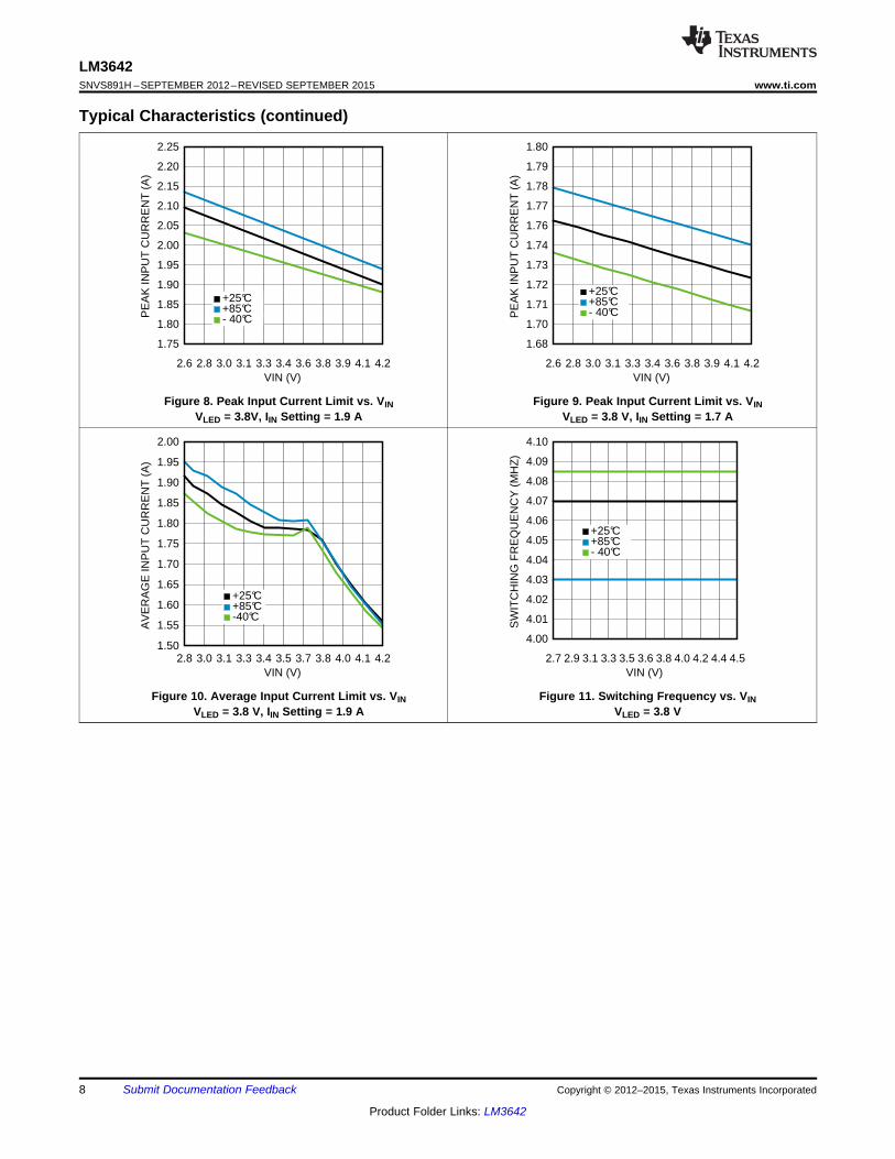
Typical Characteristics (continued)
Figure 8. Peak Input Current Limit vs. VIN Figure 9. Peak Input Current Limit vs. VINVLED = 3.8V, IIN Setting = 1.9 A VLED = 3.8 V, IIN Setting = 1.7 A
Figure 10. Average Input Current Limit vs. VIN Figure 11. Switching Frequency vs. VINVLED = 3.8 V, IIN Setting = 1.9 A VLED = 3.8 V
8 Submit Documentation Feedback Copyright © 2012–2015, Texas Instruments Incorporated
Product Folder Links: LM3642
+-
VOVP
PWM Control
ThermalShutdown
+150oC
INVREF
I2C
Interface
+
-
+ -
ErrorAmplifier
SlopeCompensation
SDA
SCL
ControlLogic/
Registers
GND
OUT
LED
STROBETORCH/TX
SW
80 m:
80 m:
Over Voltage Comparator
ILED
Soft-Start
+-
4 MHzOscillator
+-
UVLOInput Voltage Flash Monitor
OUT-VHR
Current Sense/Current Limit
LM3642www.ti.com SNVS891H –SEPTEMBER 2012–REVISED SEPTEMBER 2015
7 Detailed Description
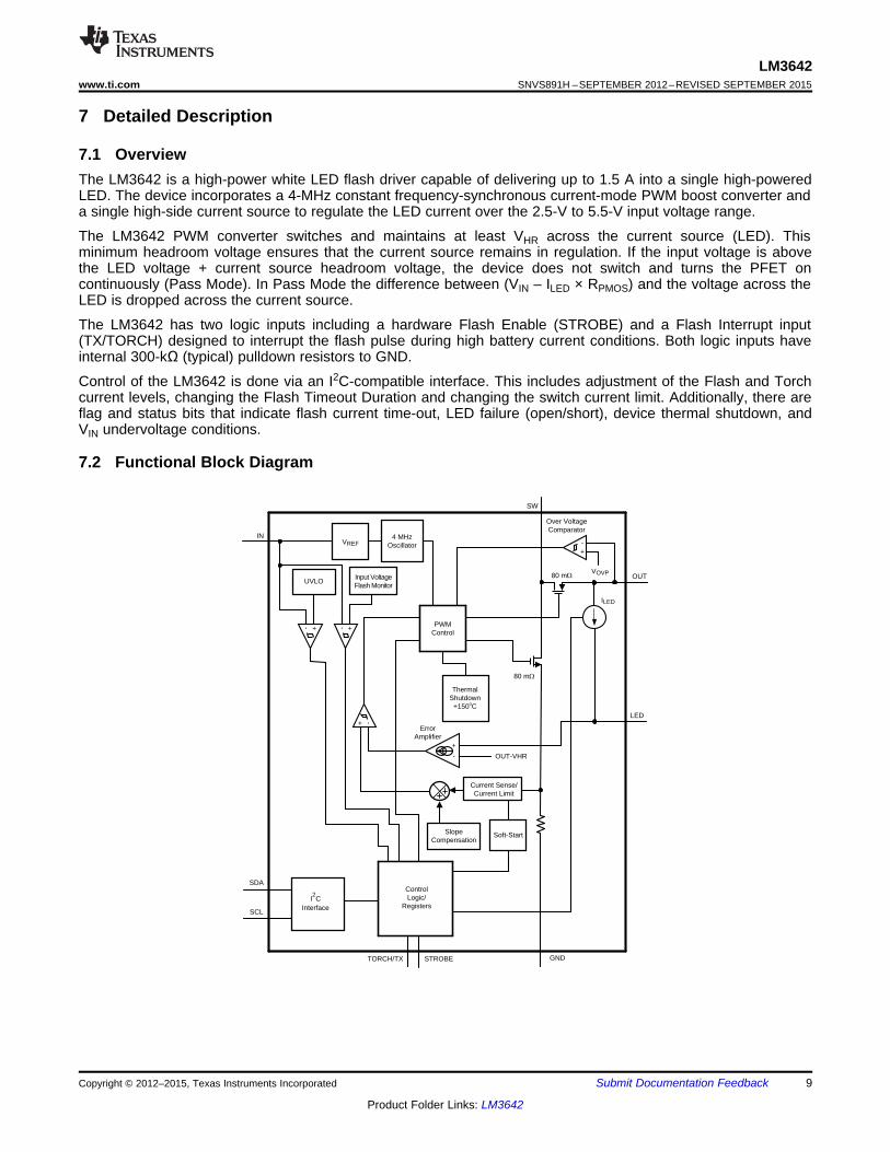
7.1 OverviewThe LM3642 is a high-power white LED flash driver capable of delivering up to 1.5 A into a single high-poweredLED. The device incorporates a 4-MHz constant frequency-synchronous current-mode PWM boost converter anda single high-side current source to regulate the LED current over the 2.5-V to 5.5-V input voltage range.
The LM3642 PWM converter switches and maintains at least VHR across the current source (LED). Thisminimum headroom voltage ensures that the current source remains in regulation. If the input voltage is abovethe LED voltage + current source headroom voltage, the device does not switch and turns the PFET oncontinuously (Pass Mode). In Pass Mode the difference between (VIN – ILED × RPMOS) and the voltage across theLED is dropped across the current source.
The LM3642 has two logic inputs including a hardware Flash Enable (STROBE) and a Flash Interrupt input(TX/TORCH) designed to interrupt the flash pulse during high battery current conditions. Both logic inputs haveinternal 300-kΩ (typical) pulldown resistors to GND.
Control of the LM3642 is done via an I2C-compatible interface. This includes adjustment of the Flash and Torchcurrent levels, changing the Flash Timeout Duration and changing the switch current limit. Additionally, there areflag and status bits that indicate flash current time-out, LED failure (open/short), device thermal shutdown, andVIN undervoltage conditions.
7.2 Functional Block Diagram
Copyright © 2012–2015, Texas Instruments Incorporated Submit Documentation Feedback 9
Product Folder Links: LM3642
LM3642SNVS891H –SEPTEMBER 2012–REVISED SEPTEMBER 2015 www.ti.com
7.3 Feature Description
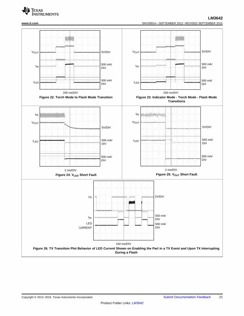
7.3.1 Power Amplifier Synchronization (TX/TORCH)The TX pin is a Power Amplifier Synchronization input. This is designed to reduce the flash LED current and thuslimit the battery current during high battery current conditions such as PA transmit events. When the LM3642 isengaged in a Flash event, and the TX pin is pulled high, the LED current is forced into Torch Mode at theprogrammed Torch current setting. If the TX pin is then pulled low before the Flash pulse terminates, the LEDcurrent will return to the previous Flash current level. At the end of the Flash time-out whether the TX pin is highor low, the LED current will turn off.
7.3.2 Input Voltage Flash Monitor (IVFM)The LM3642 has the ability to adjust the flash current based upon the voltage level present at the IN pin utilizingan Input Voltage Flash Monitor. Upon an IVFM event, the set voltage threshold from the IVFM Mode Registersets the input voltage boundary that forces the LM3642 to stop ramping the flash current during start-up (Stopand Hold Mode).
7.3.3 Fault and Protections
7.3.3.1 Fault OperationUpon entering a fault condition, the LM3642 will set the appropriate flag in the Flags Register.
7.3.3.2 Flash Time-OutThe Flash Time-Out period sets the amount of time that the Flash Current is being sourced from the currentsource (LED). The LM3642 has 8 time-out levels ranging 100 ms to 800 ms in 100-ms steps. The Flash Time-Out period is controlled in the Flash Features Register (0x08). Flash Time-Out only applies to the Flash Modeoperation. The mode bits in the Enable Register (0x0A) are cleared upon a Flash Time-out.
If an I2C command is used to terminate the flash event, TI recommends selecting a flash time-out level 100 msabove the desired flash duration.
7.3.3.3 Overvoltage Protection (OVP)The output voltage is limited to typically 5 V (see VOVP in Electrical Characteristics). In situations such as an openLED, the LM3642 will raise the output voltage in order to keep the LED current at its target value. When VOUTreaches 5 V (typ.) the overvoltage comparator will trip and turn off the internal NFET. When VOUT falls below theVOVP Off Threshold, the LM3642 begins switching again. The mode bits in the Enable Register are not clearedupon an OVP.
7.3.3.4 Current LimitThe LM3642 features selectable inductor current limits that are programmable through the Flash FeatureRegister of the I2C-compatible interface. When the inductor current limit is reached, the LM3642 will terminatethe charging phase of the switching cycle.
Since the current limit is sensed in the NMOS switch, there is no mechanism to limit the current when the deviceoperates in Pass Mode. In Boost Mode or Pass Mode if VOUT falls below 2.3 V, the part stops switching, and thePFET operates as a current source limiting the current to 300 mA. This prevents damage to the LM3642 andexcessive current draw from the battery during output short-circuit conditions. The mode bits in the EnableRegister (0x0A) are not cleared upon a Current Limit event.
NOTEPulling additional current from the VOUT node during normal operation is notrecommended.
10 Submit Documentation Feedback Copyright © 2012–2015, Texas Instruments Incorporated
Product Folder Links: LM3642
LM3642www.ti.com SNVS891H –SEPTEMBER 2012–REVISED SEPTEMBER 2015
Feature Description (continued)7.3.3.5 Undervoltage Lockout (UVLO)The LM3642 has an internal comparator that monitors the voltage at IN which will force the LM3642 intoshutdown if the input voltage drops to 2.8 V. If the UVLO monitor threshold is tripped, the UVLO flag bit will beset in the Flags Register. If the input voltage rises above 2.8 V, the LM3642 will not be available for operationuntil there is an I2C read command initiated for the Flags Register. Upon a read, the flag register will be cleared,and normal operation can resume. This feature can be disabled by writing a ‘0’ to the UVLO EN bit in the InputVoltage Flash Monitor Register. The mode bits in the Enable Register are cleared upon a UVLO event.
7.3.3.6 Thermal Shutdown (TSD)When the LM3642 device’s die temperature reaches 150°C the boost converter shuts down, and the NFET andPFET turn off, as does the current source (LED). When the thermal shutdown threshold is tripped, a '1' getswritten to the corresponding bit of the Flags Register (Thermal Shutdown bit), and the LM3642 will go intostandby. The LM3642 will only be allowed to restart after the Flags Register is read, clearing the fault flag. Uponrestart, if the die temperature is still above 150°C, the LM3642 will reset the fault flag and re-enter standby. Themode bits in the Enable Register are cleared upon a TSD.
7.3.3.7 LED and/or VOUT FaultThe LED Fault flag in the Flags Register reads back a '1' if the part is active in Flash or Torch Mode and the LEDoutput or the VOUT node experiences short condition. The LM3642 determines an LED open condition if the OVPthreshold is crossed at the OUT pin while the device is in Flash or Torch Mode. An LED short condition isdetermined if the voltage at LED goes below 500 mV (typ.) while the device is in Torch or Flash Mode. There is adelay of 256-μs deglitch time before the LED flag is valid and 2.048 ms before the VOUT flag is valid. This delay isthe time between when the Flash or Torch current is triggered and when the LED voltage and the output voltageis sampled. The LED flag can be reset by reading back the flags register. The mode bits in the Enable Registerare cleared upon an LED and/or VOUT fault.
7.4 Device Functional Modes
7.4.1 Start-up (Enabling the Device)Turnon of the LM3642 Torch and Flash Modes can be done through the Enable Register. On start-up, whenVOUT is less than VIN the internal synchronous PFET turns on as a current source and delivers 350 mA (typ.) tothe output capacitor. During this time the current source (LED) is off. When the voltage across the outputcapacitor reaches 2.2V (typ.), the current source will turn on. At turnon the current source will step through eachFlash or Torch level until the target LED current is reached. This gives the device a controlled turnon and limitsinrush current from the VIN supply.
7.4.2 Pass ModeThe LM3642 starts up in Pass Mode and stays there until Boost Mode is needed to maintain regulation. If thevoltage difference between VOUT and VLED falls below VHR, the device switches to Boost Mode. In Pass Mode theboost converter does not switch and the synchronous PFET turns fully on bringing VOUT up to VIN – ILED × RPMOS.In Pass Mode the inductor current is not limited by the peak current limit. In this situation the output current mustbe limited to 2 A.
7.4.3 Flash ModeIn Flash Mode, the LED current source (LED) provides 16 target current levels from 93.75 mA to 1500 mA. TheFlash currents are adjusted via the Current Control Register. Flash Mode is activated by the Enable Register, orby pulling the STROBE pin HIGH. Once the Flash sequence is activated the current source (LED) will ramp up tothe programmed Flash current by stepping through all current steps until the programmed current is reached.
When the part is enabled in the Flash Mode through the Enable Register, all mode bits in the Enable Registerare cleared after a flash time-out event.
Table 1 shows the I2C commands and the state of the mode bits, if the STROBE pin is used to enable the FlashMode.
Copyright © 2012–2015, Texas Instruments Incorporated Submit Documentation Feedback 11
Product Folder Links: LM3642
SCL
SDA
data change allowed
data valid
data change allowed
data valid
data change allowed
LM3642SNVS891H –SEPTEMBER 2012–REVISED SEPTEMBER 2015 www.ti.com
Device Functional Modes (continued)Table 1. Status of Mode Bits
MODE CHANGE REQUIRED STATUS OF MODE BITS IN THE ENABLE REGISTER AFTER A FLASHUsing Level Triggered STROBE to Flash Mode bits are cleared after a single flash. To reflash, 0x23 will have to be written
to 0x0A.
7.4.4 Torch ModeIn Torch Mode, the current source (LED) is programmed via the Current Control Register. Torch Mode isactivated by the Enable Register and/or by Enabling the part in TX/Torch pin configuration. Once the Torch Modeis enabled the current source will ramp up to the programmed Torch current level. The Ramp-Up and Ramp-Down times are independently adjustable via the Torch Ramp Register. Torch Mode is not affected by FlashTimeout. In the LM3642, the programmable torch current ranges from 48.4 mA to 375 mA. With the LM3642LToption, the programmable torch current ranges from 24 mA to 187 mA.
7.4.5 Indicator ModeThis mode is activated by the Enable Register. The LM3642 can be programmed to a current level that is 1/8ththe torch current value in the Current Control Register. LM3642LT has only one setting of indicator current at 5mA.
7.5 Programming
7.5.1 I2C-Compatible Interface
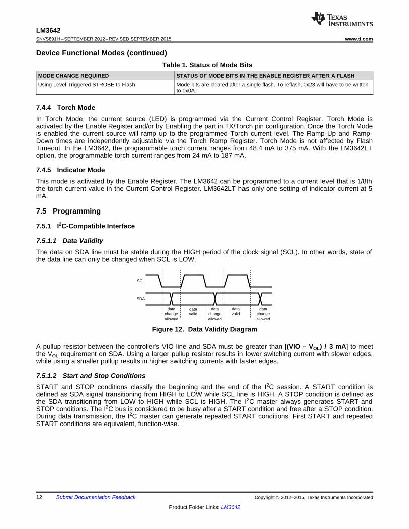
7.5.1.1 Data ValidityThe data on SDA line must be stable during the HIGH period of the clock signal (SCL). In other words, state ofthe data line can only be changed when SCL is LOW.
Figure 12. Data Validity Diagram
A pullup resistor between the controller's VIO line and SDA must be greater than [(VIO – VOL) / 3 mA] to meetthe VOL requirement on SDA. Using a larger pullup resistor results in lower switching current with slower edges,while using a smaller pullup results in higher switching currents with faster edges.
7.5.1.2 Start and Stop ConditionsSTART and STOP conditions classify the beginning and the end of the I2C session. A START condition isdefined as SDA signal transitioning from HIGH to LOW while SCL line is HIGH. A STOP condition is defined asthe SDA transitioning from LOW to HIGH while SCL is HIGH. The I2C master always generates START andSTOP conditions. The I2C bus is considered to be busy after a START condition and free after a STOP condition.During data transmission, the I2C master can generate repeated START conditions. First START and repeatedSTART conditions are equivalent, function-wise.
12 Submit Documentation Feedback Copyright © 2012–2015, Texas Instruments Incorporated
Product Folder Links: LM3642
R/WBit 0
1Bit 1
1Bit 2
0Bit 3
0Bit 4
0Bit 5
1Bit 7
1Bit 6
MSB LSB
I2C Slave Address (chip address)
start msb Chip Address lsb w ack msb Register Add lsb ack msb DATA lsb ack stop
ack from slave ack from slave ack from slave
SCL
SDA
start Id = 63h w ack addr = 0Ah ack ackData = 03h stop
SDA
Start Condition Stop Condition
SCLS P
LM3642www.ti.com SNVS891H –SEPTEMBER 2012–REVISED SEPTEMBER 2015
Programming (continued)
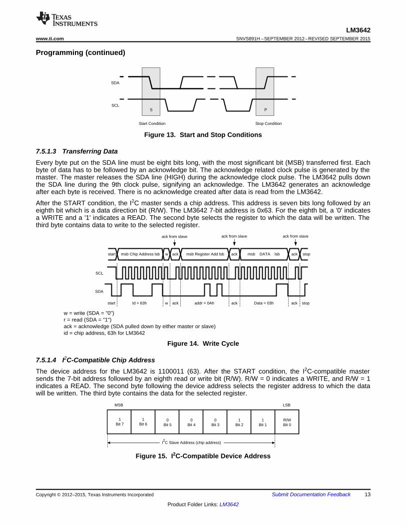
Figure 13. Start and Stop Conditions
7.5.1.3 Transferring DataEvery byte put on the SDA line must be eight bits long, with the most significant bit (MSB) transferred first. Eachbyte of data has to be followed by an acknowledge bit. The acknowledge related clock pulse is generated by themaster. The master releases the SDA line (HIGH) during the acknowledge clock pulse. The LM3642 pulls downthe SDA line during the 9th clock pulse, signifying an acknowledge. The LM3642 generates an acknowledgeafter each byte is received. There is no acknowledge created after data is read from the LM3642.
After the START condition, the I2C master sends a chip address. This address is seven bits long followed by aneighth bit which is a data direction bit (R/W). The LM3642 7-bit address is 0x63. For the eighth bit, a '0' indicatesa WRITE and a '1' indicates a READ. The second byte selects the register to which the data will be written. Thethird byte contains data to write to the selected register.
w = write (SDA = "0")r = read (SDA = "1")ack = acknowledge (SDA pulled down by either master or slave)id = chip address, 63h for LM3642
Figure 14. Write Cycle
7.5.1.4 I2C-Compatible Chip AddressThe device address for the LM3642 is 1100011 (63). After the START condition, the I2C-compatible mastersends the 7-bit address followed by an eighth read or write bit (R/W). R/W = 0 indicates a WRITE, and R/W = 1indicates a READ. The second byte following the device address selects the register address to which the datawill be written. The third byte contains the data for the selected register.
Figure 15. I2C-Compatible Device Address
Copyright © 2012–2015, Texas Instruments Incorporated Submit Documentation Feedback 13
Product Folder Links: LM3642
LM3642SNVS891H –SEPTEMBER 2012–REVISED SEPTEMBER 2015 www.ti.com
Programming (continued)7.5.1.5 Transferring DataEvery byte on the SDA line must be eight bits long, with the most significant bit (MSB) transferred first. Each byteof data must be followed by an acknowledge bit (ACK). The acknowledge related clock pulse (9th clock pulse) isgenerated by the master. The master releases SDA (HIGH) during the 9th clock pulse. The LM3642 pulls downSDA during the 9th clock pulse, signifying an acknowledge. An acknowledge is generated after each byte hasbeen received.
14 Submit Documentation Feedback Copyright © 2012–2015, Texas Instruments Incorporated
Product Folder Links: LM3642
LM3642www.ti.com SNVS891H –SEPTEMBER 2012–REVISED SEPTEMBER 2015
7.6 Register Map
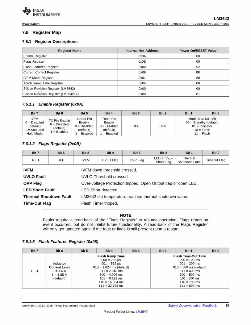
7.6.1 Register Descriptions
Register Name Internal Hex Address Power On/RESET ValueEnable Register 0x0A 00Flags Register 0x0B 00Flash Features Register 0x08 52Current Control Register 0x09 0FIVFM Mode Register 0x01 80Torch Ramp Time Register 0x06 00Silicon Revision Register (LM3642) 0x00 00Silicon Revision Register (LM3642LT) 0x00 01
7.6.1.1 Enable Register (0x0A)
Bit 7 Bit 6 Bit 5 Bit 4 Bit 3 Bit 2 Bit 1 Bit 0IVFM Strobe Pin Torch Pin Mode Bits: M1, M0TX Pin Enable0 = Disabled Enable Enable 00 = Standby (default)0 = Disabled(default) 0 = Disabled 0 = Disabled RFU RFU 01 = Indicator(default)1 = Stop and (default) (default) 10 = Torch1 = EnabledHold Mode 1 = Enabled 1 = Enabled 11 = Flash
7.6.1.2 Flags Register (0x0B)
Bit 7 Bit 6 Bit 5 Bit 4 Bit 3 Bit 2 Bit 1 Bit 0LED or VOUT ThermalRFU RFU IVFM UVLO Flag OVP Flag Timeout FlagShort Flag Shutdown Fault
IVFM IVFM down threshold crossed.UVLO Fault UVLO Threshold crossed.OVP Flag Over-voltage Protection tripped. Open Output cap or open LED.LED Short Fault LED Short detected.Thermal Shutdown Fault LM3642 die temperature reached thermal shutdown value.Time-Out Flag Flash Timer tripped.
NOTEFaults require a read-back of the “Flags Register” to resume operation. Flags report anevent occurred, but do not inhibit future functionality. A read-back of the Flags Registerwill only get updated again if the fault or flags is still present upon a restart.
7.6.1.3 Flash Features Register (0x08)
Bit 7 Bit 6 Bit 5 Bit 4 Bit 3 Bit 2 Bit 1 Bit 0Flash Ramp Time Flash Time-Out Time
000 = 256 µs 000 = 100 msInductor 001 = 512 µs 001 = 200 ms
Current Limit 010 = 1.024 ms (default) 010 = 300 ms (default)RFU 0 = 1.6 A 011 = 2.048 ms 011 = 400 ms
1 = 1.88 A 100 = 4.096 ms 100 = 500 ms(default) 101 = 8.192 ms 101 =600 ms
110 = 16.384 ms 110 = 700 ms111 = 32.768 ms 111 = 800 ms
Copyright © 2012–2015, Texas Instruments Incorporated Submit Documentation Feedback 15
Product Folder Links: LM3642
IVM-D
Deglitch
time
VIN
ILED
t
0 mA
IFLASH
LM3642SNVS891H –SEPTEMBER 2012–REVISED SEPTEMBER 2015 www.ti.com
7.6.1.4 Current Control Register (0x09)
Bit 7 Bit 6 Bit 5 Bit 4 Bit 3 Bit 2 Bit 1 Bit 0Flash Current
0000 = 93.75 mA0001 = 187.5 mA0010 = 281.25 mA
Torch Current (LM3642LT) 0011 = 375 mA000 = 48.4 mA (default) (24 mA) 0100 = 468.75 mA
001 =93.74 mA (46.87 mA) 0101 = 562.5 mA010 =140.63 mA (70.315 mA) 0110 = 656.25 mA
RFU 011 = 187.5 mA (93.25 mA) 0111 = 750 mA100 =234.38 mA (117.19 mA) 1000 = 843.75 mA
101 = 281.25 mA (140.625 mA) 1001 = 937.5 mA110 = 328.13 mA (164.075 mA) 1010 = 1031.25 mA
111 = 375 mA (187.5 mA) 1011 = 1125 mA1100 = 1218.75 mA1101 = 1312.5 mA1110 = 1406.25 mA
1111 = 1500 mA (default)
7.6.1.5 Input Voltage Flash Monitor (IVFM) Mode Register (0x01)
Bit 7 Bit 6 Bit 5 Bit 4 Bit 3 Bit 2 Bit 1 Bit 0IVM-D (Down) Threshold
000 = 2.9 V (default)001 = 3.0 VUVLO 010 =3.1 V0 = Disabled RFU 011 = 3.2 V RFU1= Enabled 100 = 3.3 V(default) 101 = 3.4 V110 = 3.5 V111 = 3.6 V
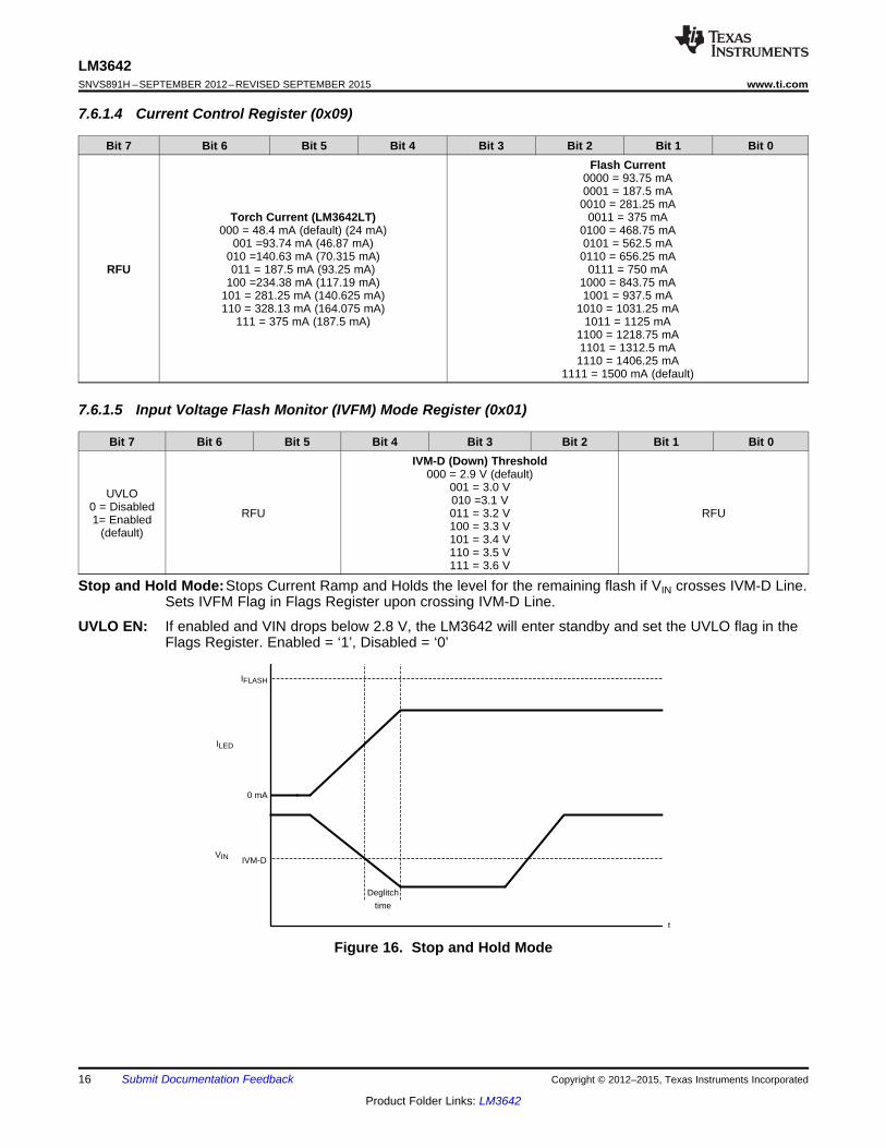
Stop and Hold Mode:Stops Current Ramp and Holds the level for the remaining flash if VIN crosses IVM-D Line.Sets IVFM Flag in Flags Register upon crossing IVM-D Line.
UVLO EN: If enabled and VIN drops below 2.8 V, the LM3642 will enter standby and set the UVLO flag in theFlags Register. Enabled = ‘1’, Disabled = ‘0’
Figure 16. Stop and Hold Mode
16 Submit Documentation Feedback Copyright © 2012–2015, Texas Instruments Incorporated
Product Folder Links: LM3642
LM3642www.ti.com SNVS891H –SEPTEMBER 2012–REVISED SEPTEMBER 2015
7.6.1.6 Torch Ramp Time Register (0x06)
Bit 7 Bit 6 Bit 5 Bit 4 Bit 3 Bit 2 Bit 1) Bit 0Torch Ramp-Up Time Torch Ramp-Down Time000 = 16 ms (default) 000 = 16 ms (default)
001 = 32 ms 001 = 32 ms010 = 64 ms 010 = 64 ms
RFU RFU 011 = 128 ms 011 = 128 ms100 = 256 ms 100 = 256 ms101 = 512 ms 101 = 512 ms110 = 1.024s 110 = 1.024s111 = 2.048s 111 = 2.048s
7.6.1.7 Silicon Revision Register
Bit 7 Bit 6 Bit 5 Bit 4 Bit 3 Bit 2 Bit 1 Bit 0RFU 000 = LM3642
Copyright © 2012–2015, Texas Instruments Incorporated Submit Documentation Feedback 17
Product Folder Links: LM3642
IN OUTSW
TX/TORCHSDASCL
1 PH
10 PF 10 PF
STROBE LED
Flash LED
2.5V to 5.5V
GND
LM3642SNVS891H –SEPTEMBER 2012–REVISED SEPTEMBER 2015 www.ti.com
8 Application and Implementation
NOTEInformation in the following applications sections is not part of the TI componentspecification, and TI does not warrant its accuracy or completeness. TI’s customers areresponsible for determining suitability of components for their purposes. Customers shouldvalidate and test their design implementation to confirm system functionality.
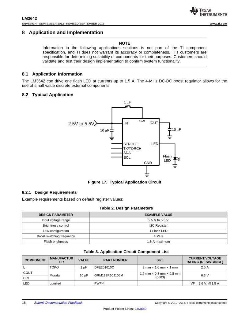
8.1 Application InformationThe LM3642 can drive one flash LED at currents up to 1.5 A. The 4-MHz DC-DC boost regulator allows for theuse of small value discrete external components.
8.2 Typical Application
Figure 17. Typical Application Circuit
8.2.1 Design RequirementsExample requirements based on default register values:
Table 2. Design ParametersDESIGN PARAMETER EXAMPLE VALUE
Input voltage range 2.5 V to 5.5 VBrightness control I2C RegisterLED configuration 1 Flash LED
Boost switching frequency 4 MHzFlash brightness 1.5 A maximum
Table 3. Application Circuit Component ListMANUFACTUR CURRENT/VOLTAGECOMPONENT VALUE PART NUMBER SIZEER RATING (RESISTANCE)
L TOKO 1 µH DFE201610C 2 mm × 1.6 mm × 1 mm 2.5 ACOUT 1.6 mm × 0.8 mm × 0.8 mmMurata 10 µF GRM188R60J106M 6.3 V(0603)CINLED Lumiled PWF-4 VF = 3.6 V, @1.5 A
18 Submit Documentation Feedback Copyright © 2012–2015, Texas Instruments Incorporated
Product Folder Links: LM3642
where IN INOUT
( )- VVxVL =I'
OUTSW VxLxfx2
I+xR=V LESRESR ''VxI OUTLED
VIN ¹·
©§
Q =V'( )INOUTLED - VVxI
OUTOUTSW CxVxf
LM3642www.ti.com SNVS891H –SEPTEMBER 2012–REVISED SEPTEMBER 2015
8.2.2 Detailed Design Procedure
8.2.2.1 Output Capacitor SelectionThe LM3642 is designed to operate with at least a 10-µF ceramic output capacitor. When the boost converter isrunning the output capacitor supplies the load current during the boost converter's on-time. When the NMOSswitch turns off the inductor energy is discharged through the internal PMOS switch, supplying power to the loadand restoring charge to the output capacitor. This causes a sag in the output voltage during the on-time and arise in the output voltage during the off-time. The output capacitor is therefore chosen to limit the output ripple toan acceptable level depending on load current and input/output voltage differentials and also to ensure theconverter remains stable.
For proper operation the output capacitor must be at least a 10-µF ceramic. Larger capacitors such as a 22-µFcapacitor or capacitors in parallel can be used if lower output voltage ripple is desired. To estimate the outputvoltage ripple considering the ripple due to capacitor discharge (ΔVQ) and the ripple due to the capacitors ESR(ΔVESR) use the following equations:
For continuous conduction mode, the output voltage ripple due to the capacitor discharge is:
(1)
The output voltage ripple due to the output capacitors ESR is found by:
(2)
In ceramic capacitors the ESR is very low so a close approximation is to assume that 80% of the output voltageripple is due to capacitor discharge and 20% from ESR. Table 4 lists different manufacturers for various outputcapacitors and their case sizes suitable for use with the LM3642.
8.2.2.2 Input Capacitor SelectionChoosing the correct size and type of input capacitor helps minimize the voltage ripple caused by the switchingof the LM3642 device’s boost converter, and reduces noise on the boost converter's input terminal that can feedthrough and disrupt internal analog signals. In the typical application circuit a 10-µF ceramic input capacitorworks well. It is important to place the input capacitor as close as possible to the LM3642 device’s input (IN) pin.This reduces the series resistance and inductance that can inject noise into the device due to the input switchingcurrents. Table 4 lists various input capacitors that are recommended for use with the LM3642.
Table 4. Recommended Input and Output Capacitors (X5R/X7R Dielectric)MANUFACTURER PART NUMBER VALUE CASE SIZE VOLTAGE RATINGTDK Corporation C1608JB0J106M 10 µF 0603 (1.6 mm × 0.8 mm × 0.8 mm) 6.3 VTDK Corporation C2012JB1A106M 10 µF 0805 (2 mm × 1.25 mm × 1.25 mm) 10 VTDK Corporation C2012JB0J226M 22 µF 0805 (2 mm × 1.25 mm × 1.25 mm) 6.3 V
Murata GRM188R60J106M 10 µF 0603 (1.6 mm × 0.8 mm × 0.8 mm) 6.3 VMurata GRM21BR61A106KE19 10 µF 0805 (2 mm × 1.25 mm × 1.25 mm) 10 VMurata GRM21BR60J226ME39L 22 µF 0805 (2 mm × 1.25 mm × 1.25 mm) 6.3 V
8.2.2.3 Inductor SelectionThe LM3642 is designed to use a 1-µH or 0.47-µH inductor. Table 5 lists various inductors and theirmanufacturers that can work well with the LM3642. When the device is boosting (VOUT > VIN) the inductor willtypically be the largest area of efficiency loss in the circuit. Therefore, choosing an inductor with the lowestpossible series resistance is important. Additionally, the saturation rating of the inductor should be greater thanthe maximum operating peak current of the LM3642. This prevents excess efficiency loss that can occur withinductors that operate in saturation. For proper inductor operation and circuit performance, ensure that theinductor saturation and the peak current limit setting of the LM3642 are greater than IPEAK in the followingcalculation:
Copyright © 2012–2015, Texas Instruments Incorporated Submit Documentation Feedback 19
Product Folder Links: LM3642
500 mA/DIV
VIN
ILED
200 mV/DIV
200 s/DIV
500 mA/DIV
VOUT
ILED
5V/DIV
200 ms/DIV
IIN500 mA/DIV
3.5 3.8 4.0 4.3 4.5 4.8 5.0
10
20
30
40
50
60
70
80
90
100
LED
EF
FIC
IEN
CY
(%
)
VIN (V)
+25°C+85°C-40°C
2.8 3.0 3.1 3.3 3.4 3.5 3.7 3.8 4.0 4.1 4.2
30
40
50
60
70
80
90
100
LED
EF
FIC
IEN
CY
(%
)
VIN (V)
+25°C+85°C-40°C
PEAKI LOADI=
Kx LI+' where L =I' IN xV ( )INOUT - VV
OUTSW VxLxfx2IN
OUT
V
V
LM3642SNVS891H –SEPTEMBER 2012–REVISED SEPTEMBER 2015 www.ti.com
(3)
where ƒSW = 4 MHz, and efficiency can be found in the Typical Characteristics plots.
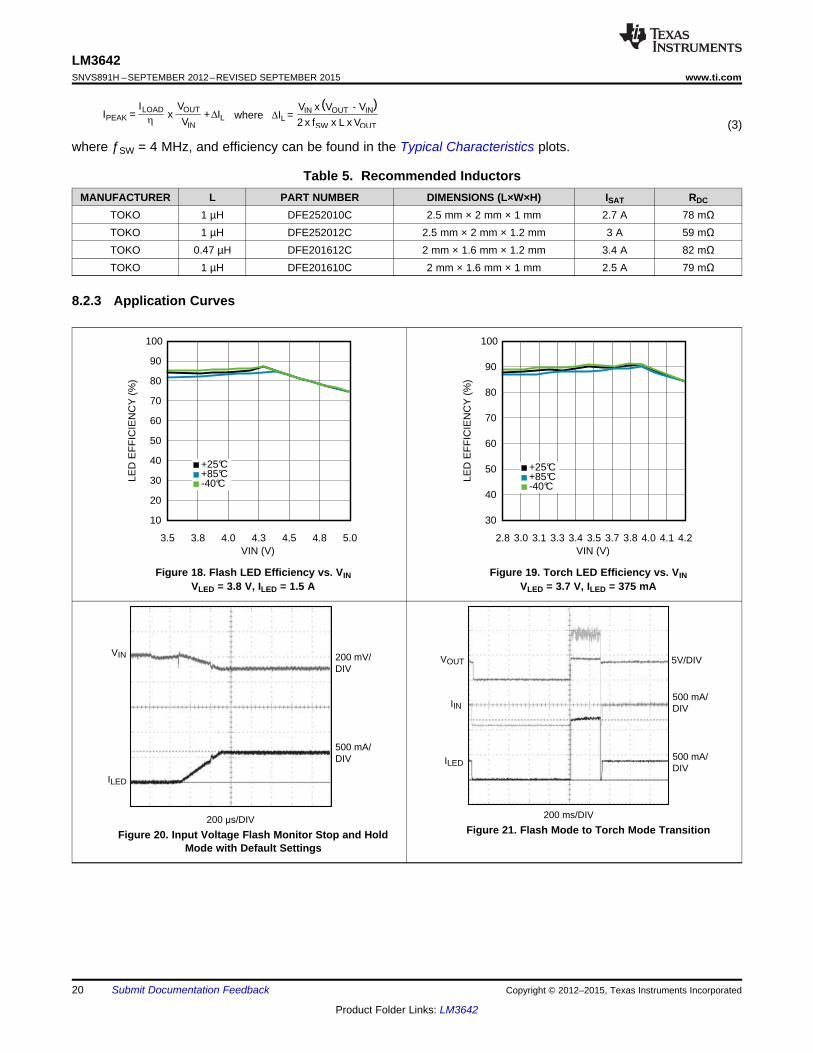
Table 5. Recommended InductorsMANUFACTURER L PART NUMBER DIMENSIONS (L×W×H) ISAT RDC
TOKO 1 µH DFE252010C 2.5 mm × 2 mm × 1 mm 2.7 A 78 mΩTOKO 1 µH DFE252012C 2.5 mm × 2 mm × 1.2 mm 3 A 59 mΩTOKO 0.47 µH DFE201612C 2 mm × 1.6 mm × 1.2 mm 3.4 A 82 mΩTOKO 1 µH DFE201610C 2 mm × 1.6 mm × 1 mm 2.5 A 79 mΩ
8.2.3 Application Curves
Figure 18. Flash LED Efficiency vs. VIN Figure 19. Torch LED Efficiency vs. VINVLED = 3.8 V, ILED = 1.5 A VLED = 3.7 V, ILED = 375 mA
Figure 21. Flash Mode to Torch Mode TransitionFigure 20. Input Voltage Flash Monitor Stop and HoldMode with Default Settings
20 Submit Documentation Feedback Copyright © 2012–2015, Texas Instruments Incorporated
Product Folder Links: LM3642
500 mA/DIV
TX
LED
CURRENT
2V/DIV
100 ms/DIV
IIN500 mA/DIV
500 mA/DIV
VOUT
ILED
5V/DIV
2 ms/DIV
IIN
500 mA/DIV
500 mA/DIV
VOUT
ILED
5V/DIV
2 ms/DIV
IIN
500 mA/DIV
500 mA/DIV
VOUT
ILED
5V/DIV
200 ms/DIV
IIN500 mA/DIV
500 mA/DIV
VOUT
ILED
5V/DIV
200 ms/DIV
IIN500 mA/DIV
LM3642www.ti.com SNVS891H –SEPTEMBER 2012–REVISED SEPTEMBER 2015
Figure 22. Torch Mode to Flash Mode Transition Figure 23. Indicator Mode - Torch Mode - Flash ModeTransitions
Figure 25. VOUT Short FaultFigure 24. VLED Short Fault
Figure 26. TX Transition Plot Behavior of LED Current Shown on Enabling the Part in a TX Event and Upon TX InterruptingDuring a Flash
Copyright © 2012–2015, Texas Instruments Incorporated Submit Documentation Feedback 21
Product Folder Links: LM3642
LM3642SNVS891H –SEPTEMBER 2012–REVISED SEPTEMBER 2015 www.ti.com
9 Power Supply RecommendationsThe LM3642 is designed to operate from an input voltage supply range between 2.5 V and 5.5 V. This inputsupply must be well regulated and capable to supply the required input current. If the input supply is located farfrom the LM3642 additional bulk capacitance may be required in addition to the ceramic bypass capacitors.
10 Layout
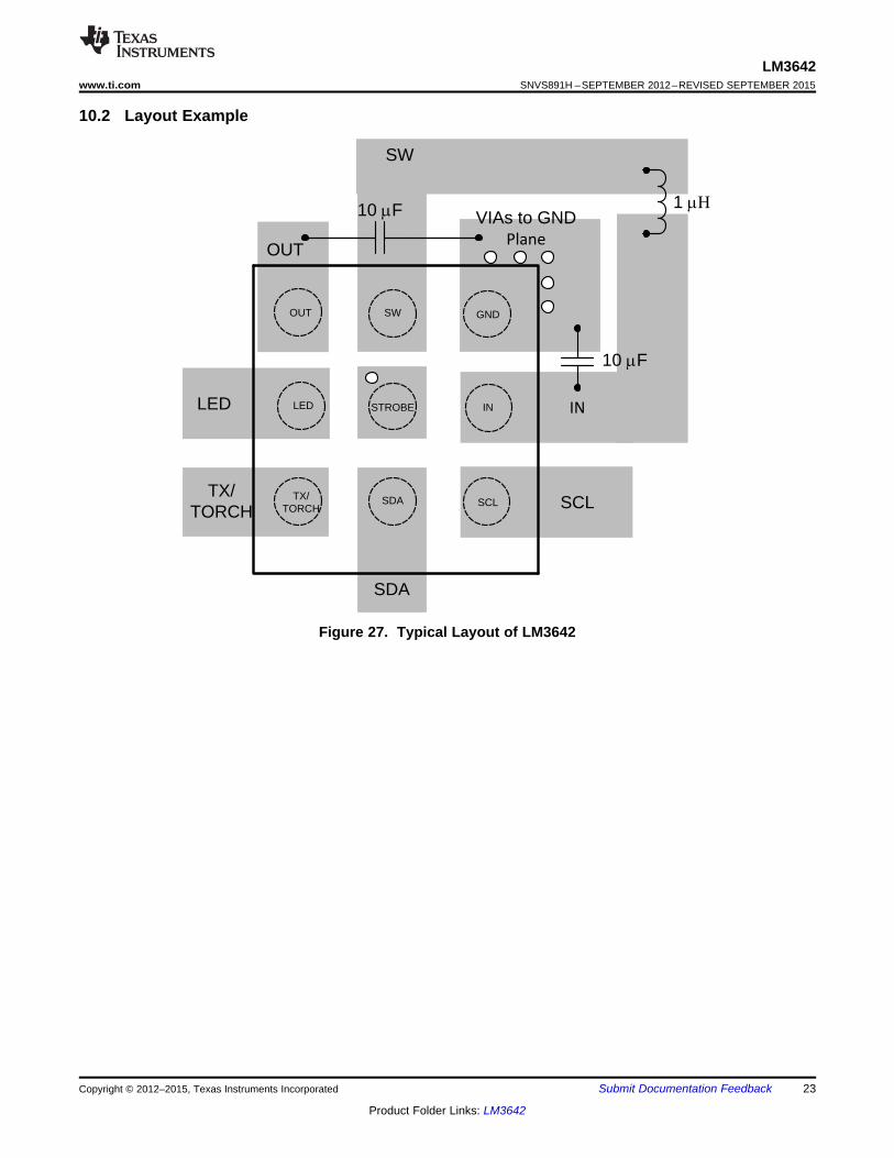
10.1 Layout GuidelinesThe high switching frequency and large switching currents of the LM3642 make the choice of layout important.The following steps should be used as a reference to ensure the device is stable and maintains proper LEDcurrent regulation across its intended operating voltage and current range.1. Place CIN on the top layer (same layer as the LM3642 and as close to the device as possible. The input
capacitor conducts the driver currents during the low side MOSFET turn-on and turn-off and can see currentspikes over 1 A in amplitude. Connecting the input capacitor through short wide traces to both the IN andGND pins will reduce the inductive voltage spikes that occur during switching and which can corrupt the VINline.
2. Place COUT on the top layer (same layer as the LM3642) and as close as possible to the OUT and GND pin.The returns for both CIN and COUT should come together at one point, and as close to the GND pin aspossible. Connecting COUT through short wide traces will reduce the series inductance on the OUT and GNDpins that can corrupt the VOUT and GND line and cause excessive noise in the device and surroundingcircuitry.
3. Connect the inductor on the top layer close to the SW pin. There should be a low-impedance connectionfrom the inductor to SW due to the large DC inductor current, and at the same time the area occupied by theSW node should be small so as to reduce the capacitive coupling of the high dV/dt present at SW that cancouple into nearby traces.
4. Avoid routing logic traces near the SW node so as to avoid any capacitively coupled voltages from SW ontoany high-impedance logic lines such as STROBE, SDA, and SCL. A good approach is to insert an inner layerGND plane underneath the SW node and between any nearby routed traces. This creates a shield from theelectric field generated at SW.
5. Terminate the Flash LED cathodes directly to the GND pin of the LM3642. If possible, route the LED returnswith a dedicated path so as to keep the high amplitude LED currents out of the GND plane. For Flash LEDsthat are routed relatively far away from the LM3642, a good approach is to sandwich the forward and returncurrent paths over the top of each other on two layers. This will help in reducing the inductance of the LEDcurrent paths.
22 Submit Documentation Feedback Copyright © 2012–2015, Texas Instruments Incorporated
Product Folder Links: LM3642
OUT SW
LED STROBE IN
GND
SDATX/TORCH
SCL
10 PF
1 P+
TX/TORCH
LED IN
SDA
OUT
VIAs to GNDPlane
SW
10 PF
SCL
LM3642www.ti.com SNVS891H –SEPTEMBER 2012–REVISED SEPTEMBER 2015
10.2 Layout Example
Figure 27. Typical Layout of LM3642
Copyright © 2012–2015, Texas Instruments Incorporated Submit Documentation Feedback 23
Product Folder Links: LM3642
LM3642SNVS891H –SEPTEMBER 2012–REVISED SEPTEMBER 2015 www.ti.com
11 Device and Documentation Support
11.1 Device Support
11.1.1 Third-Party Products DisclaimerTI'S PUBLICATION OF INFORMATION REGARDING THIRD-PARTY PRODUCTS OR SERVICES DOES NOTCONSTITUTE AN ENDORSEMENT REGARDING THE SUITABILITY OF SUCH PRODUCTS OR SERVICESOR A WARRANTY, REPRESENTATION OR ENDORSEMENT OF SUCH PRODUCTS OR SERVICES, EITHERALONE OR IN COMBINATION WITH ANY TI PRODUCT OR SERVICE.
11.2 Documentation Support
11.2.1 Related DocumentationFor related documentation, see the following:
Texas Instruments Application Note 1112: DSBGA Wafer Level Chip Scale Package (SNVA009).
11.3 TrademarksE2E is a trademark of Texas Instruments.All other trademarks are the property of their respective owners.
11.4 Community ResourcesThe following links connect to TI community resources. Linked contents are provided "AS IS" by the respectivecontributors. They do not constitute TI specifications and do not necessarily reflect TI's views; see TI's Terms ofUse.
TI E2E™ Online Community TI's Engineer-to-Engineer (E2E) Community. Created to foster collaborationamong engineers. At e2e.ti.com, you can ask questions, share knowledge, explore ideas and helpsolve problems with fellow engineers.
Design Support TI's Design Support Quickly find helpful E2E forums along with design support tools andcontact information for technical support.
11.5 Electrostatic Discharge CautionThis integrated circuit can be damaged by ESD. Texas Instruments recommends that all integrated circuits be handled withappropriate precautions. Failure to observe proper handling and installation procedures can cause damage.
ESD damage can range from subtle performance degradation to complete device failure. Precision integrated circuits may be moresusceptible to damage because very small parametric changes could cause the device not to meet its published specifications.
11.6 GlossarySLYZ022 — TI Glossary.
This glossary lists and explains terms, acronyms, and definitions.
12 Mechanical, Packaging, and Orderable InformationThe following pages include mechanical, packaging, and orderable information. This information is the mostcurrent data available for the designated devices. This data is subject to change without notice and revision ofthis document. For browser-based versions of this data sheet, refer to the left-hand navigation.
24 Submit Documentation Feedback Copyright © 2012–2015, Texas Instruments Incorporated
Product Folder Links: LM3642
PACKAGE OPTION ADDENDUM
www.ti.com 22-Sep-2016
Addendum-Page 1
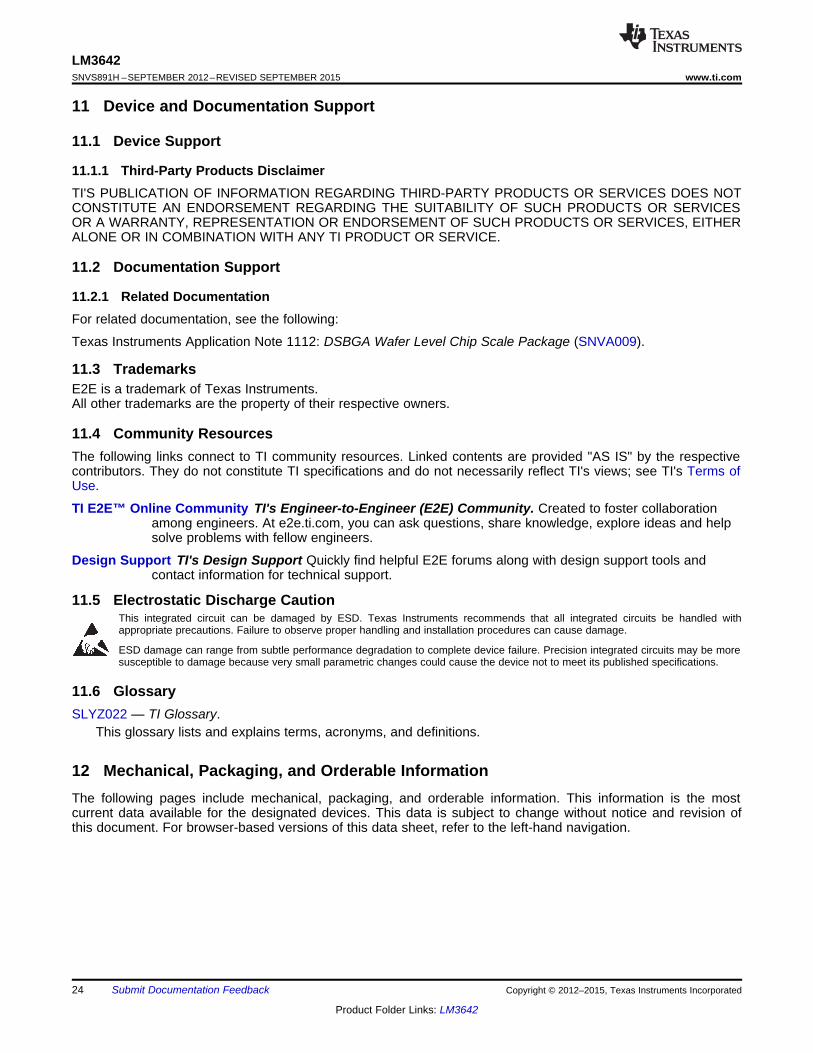
PACKAGING INFORMATION
Orderable Device Status(1)
Package Type PackageDrawing
Pins PackageQty
Eco Plan(2)
Lead/Ball Finish(6)
MSL Peak Temp(3)
Op Temp (°C) Device Marking(4/5)
Samples
LM3642TLE-LT/NOPB ACTIVE DSBGA YZR 9 250 Green (RoHS& no Sb/Br)
SNAGCU Level-1-260C-UNLIM -40 to 85 (D2 ~ D4)
LM3642TLE/NOPB ACTIVE DSBGA YZR 9 250 Green (RoHS& no Sb/Br)
SNAGCU Level-1-260C-UNLIM -40 to 85 D2
LM3642TLX-LT/NOPB ACTIVE DSBGA YZR 9 3000 Green (RoHS& no Sb/Br)
SNAGCU Level-1-260C-UNLIM -40 to 85 (D2 ~ D4)
LM3642TLX/NOPB ACTIVE DSBGA YZR 9 3000 Green (RoHS& no Sb/Br)
SNAGCU Level-1-260C-UNLIM -40 to 85 D2
(1) The marketing status values are defined as follows:ACTIVE: Product device recommended for new designs.LIFEBUY: TI has announced that the device will be discontinued, and a lifetime-buy period is in effect.NRND: Not recommended for new designs. Device is in production to support existing customers, but TI does not recommend using this part in a new design.PREVIEW: Device has been announced but is not in production. Samples may or may not be available.OBSOLETE: TI has discontinued the production of the device.
(2) Eco Plan - The planned eco-friendly classification: Pb-Free (RoHS), Pb-Free (RoHS Exempt), or Green (RoHS & no Sb/Br) - please check http://www.ti.com/productcontent for the latest availabilityinformation and additional product content details.TBD: The Pb-Free/Green conversion plan has not been defined.Pb-Free (RoHS): TI's terms "Lead-Free" or "Pb-Free" mean semiconductor products that are compatible with the current RoHS requirements for all 6 substances, including the requirement thatlead not exceed 0.1% by weight in homogeneous materials. Where designed to be soldered at high temperatures, TI Pb-Free products are suitable for use in specified lead-free processes.Pb-Free (RoHS Exempt): This component has a RoHS exemption for either 1) lead-based flip-chip solder bumps used between the die and package, or 2) lead-based die adhesive used betweenthe die and leadframe. The component is otherwise considered Pb-Free (RoHS compatible) as defined above.Green (RoHS & no Sb/Br): TI defines "Green" to mean Pb-Free (RoHS compatible), and free of Bromine (Br) and Antimony (Sb) based flame retardants (Br or Sb do not exceed 0.1% by weightin homogeneous material)
(3) MSL, Peak Temp. - The Moisture Sensitivity Level rating according to the JEDEC industry standard classifications, and peak solder temperature.
(4) There may be additional marking, which relates to the logo, the lot trace code information, or the environmental category on the device.
(5) Multiple Device Markings will be inside parentheses. Only one Device Marking contained in parentheses and separated by a "~" will appear on a device. If a line is indented then it is a continuationof the previous line and the two combined represent the entire Device Marking for that device.
(6) Lead/Ball Finish - Orderable Devices may have multiple material finish options. Finish options are separated by a vertical ruled line. Lead/Ball Finish values may wrap to two lines if the finishvalue exceeds the maximum column width.
PACKAGE OPTION ADDENDUM
www.ti.com 22-Sep-2016
Addendum-Page 2
Important Information and Disclaimer:The information provided on this page represents TI's knowledge and belief as of the date that it is provided. TI bases its knowledge and belief on informationprovided by third parties, and makes no representation or warranty as to the accuracy of such information. Efforts are underway to better integrate information from third parties. TI has taken andcontinues to take reasonable steps to provide representative and accurate information but may not have conducted destructive testing or chemical analysis on incoming materials and chemicals.TI and TI suppliers consider certain information to be proprietary, and thus CAS numbers and other limited information may not be available for release.
In no event shall TI's liability arising out of such information exceed the total purchase price of the TI part(s) at issue in this document sold by TI to Customer on an annual basis.
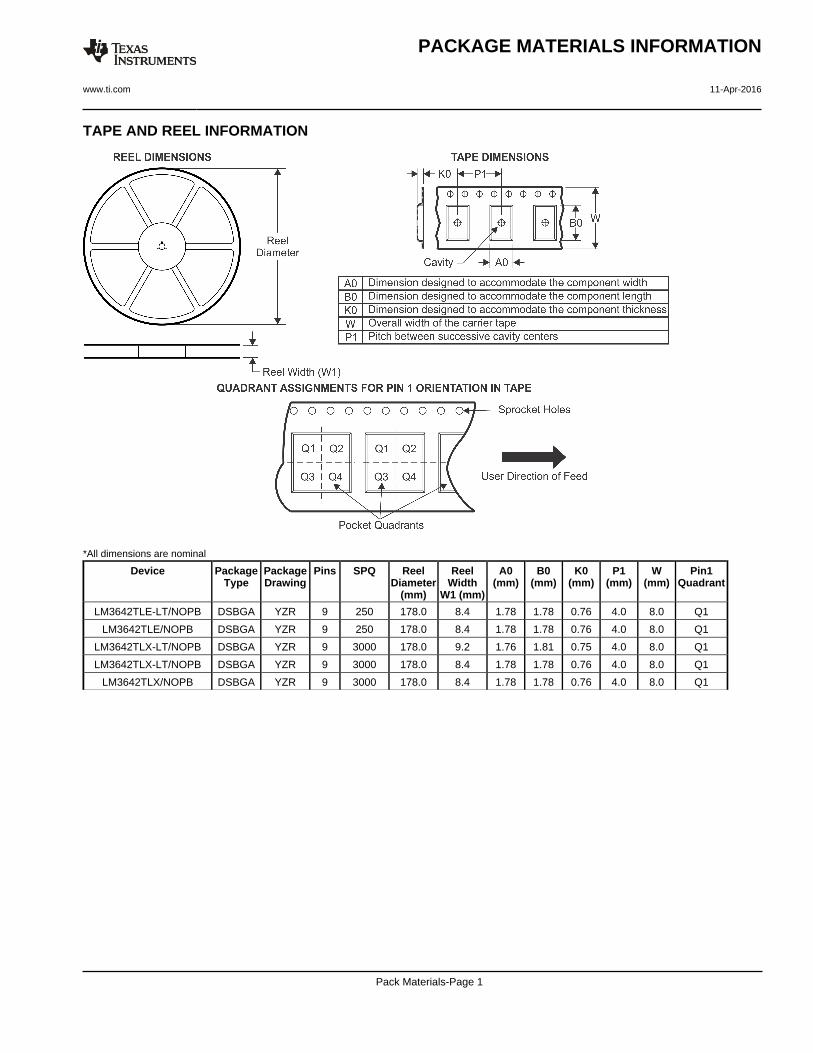
TAPE AND REEL INFORMATION
*All dimensions are nominal
Device PackageType
PackageDrawing
Pins SPQ ReelDiameter
(mm)
ReelWidth
W1 (mm)
A0(mm)
B0(mm)
K0(mm)
P1(mm)
W(mm)
Pin1Quadrant
LM3642TLE-LT/NOPB DSBGA YZR 9 250 178.0 8.4 1.78 1.78 0.76 4.0 8.0 Q1
LM3642TLE/NOPB DSBGA YZR 9 250 178.0 8.4 1.78 1.78 0.76 4.0 8.0 Q1
LM3642TLX-LT/NOPB DSBGA YZR 9 3000 178.0 9.2 1.76 1.81 0.75 4.0 8.0 Q1
LM3642TLX-LT/NOPB DSBGA YZR 9 3000 178.0 8.4 1.78 1.78 0.76 4.0 8.0 Q1
LM3642TLX/NOPB DSBGA YZR 9 3000 178.0 8.4 1.78 1.78 0.76 4.0 8.0 Q1
PACKAGE MATERIALS INFORMATION
www.ti.com 11-Apr-2016
Pack Materials-Page 1
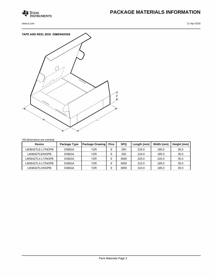
*All dimensions are nominal
Device Package Type Package Drawing Pins SPQ Length (mm) Width (mm) Height (mm)
LM3642TLE-LT/NOPB DSBGA YZR 9 250 210.0 185.0 35.0
LM3642TLE/NOPB DSBGA YZR 9 250 210.0 185.0 35.0
LM3642TLX-LT/NOPB DSBGA YZR 9 3000 220.0 220.0 35.0
LM3642TLX-LT/NOPB DSBGA YZR 9 3000 210.0 185.0 35.0
LM3642TLX/NOPB DSBGA YZR 9 3000 210.0 185.0 35.0
PACKAGE MATERIALS INFORMATION
www.ti.com 11-Apr-2016
Pack Materials-Page 2
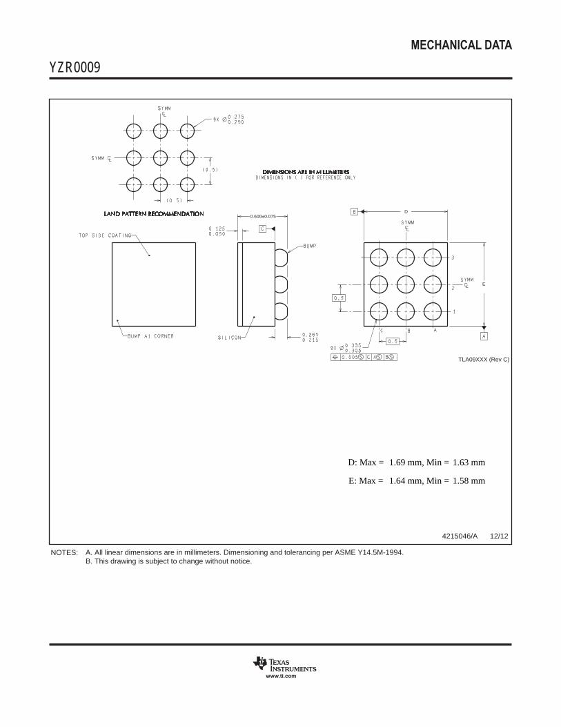
MECHANICAL DATA
YZR0009xxx
www.ti.com
TLA09XXX (Rev C)
0.600±0.075D
E
A. All linear dimensions are in millimeters. Dimensioning and tolerancing per ASME Y14.5M-1994.B. This drawing is subject to change without notice.
4215046/A 12/12
NOTES:
D: Max =
E: Max =
1.69 mm, Min =
1.64 mm, Min =
1.63 mm
1.58 mm
IMPORTANT NOTICE
Texas Instruments Incorporated (TI) reserves the right to make corrections, enhancements, improvements and other changes to itssemiconductor products and services per JESD46, latest issue, and to discontinue any product or service per JESD48, latest issue. Buyersshould obtain the latest relevant information before placing orders and should verify that such information is current and complete.TI’s published terms of sale for semiconductor products (http://www.ti.com/sc/docs/stdterms.htm) apply to the sale of packaged integratedcircuit products that TI has qualified and released to market. Additional terms may apply to the use or sale of other types of TI products andservices.Reproduction of significant portions of TI information in TI data sheets is permissible only if reproduction is without alteration and isaccompanied by all associated warranties, conditions, limitations, and notices. TI is not responsible or liable for such reproduceddocumentation. Information of third parties may be subject to additional restrictions. Resale of TI products or services with statementsdifferent from or beyond the parameters stated by TI for that product or service voids all express and any implied warranties for theassociated TI product or service and is an unfair and deceptive business practice. TI is not responsible or liable for any such statements.Buyers and others who are developing systems that incorporate TI products (collectively, “Designers”) understand and agree that Designersremain responsible for using their independent analysis, evaluation and judgment in designing their applications and that Designers havefull and exclusive responsibility to assure the safety of Designers' applications and compliance of their applications (and of all TI productsused in or for Designers’ applications) with all applicable regulations, laws and other applicable requirements. Designer represents that, withrespect to their applications, Designer has all the necessary expertise to create and implement safeguards that (1) anticipate dangerousconsequences of failures, (2) monitor failures and their consequences, and (3) lessen the likelihood of failures that might cause harm andtake appropriate actions. Designer agrees that prior to using or distributing any applications that include TI products, Designer willthoroughly test such applications and the functionality of such TI products as used in such applications.TI’s provision of technical, application or other design advice, quality characterization, reliability data or other services or information,including, but not limited to, reference designs and materials relating to evaluation modules, (collectively, “TI Resources”) are intended toassist designers who are developing applications that incorporate TI products; by downloading, accessing or using TI Resources in anyway, Designer (individually or, if Designer is acting on behalf of a company, Designer’s company) agrees to use any particular TI Resourcesolely for this purpose and subject to the terms of this Notice.TI’s provision of TI Resources does not expand or otherwise alter TI’s applicable published warranties or warranty disclaimers for TIproducts, and no additional obligations or liabilities arise from TI providing such TI Resources. TI reserves the right to make corrections,enhancements, improvements and other changes to its TI Resources. TI has not conducted any testing other than that specificallydescribed in the published documentation for a particular TI Resource.Designer is authorized to use, copy and modify any individual TI Resource only in connection with the development of applications thatinclude the TI product(s) identified in such TI Resource. NO OTHER LICENSE, EXPRESS OR IMPLIED, BY ESTOPPEL OR OTHERWISETO ANY OTHER TI INTELLECTUAL PROPERTY RIGHT, AND NO LICENSE TO ANY TECHNOLOGY OR INTELLECTUAL PROPERTYRIGHT OF TI OR ANY THIRD PARTY IS GRANTED HEREIN, including but not limited to any patent right, copyright, mask work right, orother intellectual property right relating to any combination, machine, or process in which TI products or services are used. Informationregarding or referencing third-party products or services does not constitute a license to use such products or services, or a warranty orendorsement thereof. Use of TI Resources may require a license from a third party under the patents or other intellectual property of thethird party, or a license from TI under the patents or other intellectual property of TI.TI RESOURCES ARE PROVIDED “AS IS” AND WITH ALL FAULTS. TI DISCLAIMS ALL OTHER WARRANTIES ORREPRESENTATIONS, EXPRESS OR IMPLIED, REGARDING RESOURCES OR USE THEREOF, INCLUDING BUT NOT LIMITED TOACCURACY OR COMPLETENESS, TITLE, ANY EPIDEMIC FAILURE WARRANTY AND ANY IMPLIED WARRANTIES OFMERCHANTABILITY, FITNESS FOR A PARTICULAR PURPOSE, AND NON-INFRINGEMENT OF ANY THIRD PARTY INTELLECTUALPROPERTY RIGHTS. TI SHALL NOT BE LIABLE FOR AND SHALL NOT DEFEND OR INDEMNIFY DESIGNER AGAINST ANY CLAIM,INCLUDING BUT NOT LIMITED TO ANY INFRINGEMENT CLAIM THAT RELATES TO OR IS BASED ON ANY COMBINATION OFPRODUCTS EVEN IF DESCRIBED IN TI RESOURCES OR OTHERWISE. IN NO EVENT SHALL TI BE LIABLE FOR ANY ACTUAL,DIRECT, SPECIAL, COLLATERAL, INDIRECT, PUNITIVE, INCIDENTAL, CONSEQUENTIAL OR EXEMPLARY DAMAGES INCONNECTION WITH OR ARISING OUT OF TI RESOURCES OR USE THEREOF, AND REGARDLESS OF WHETHER TI HAS BEENADVISED OF THE POSSIBILITY OF SUCH DAMAGES.Unless TI has explicitly designated an individual product as meeting the requirements of a particular industry standard (e.g., ISO/TS 16949and ISO 26262), TI is not responsible for any failure to meet such industry standard requirements.Where TI specifically promotes products as facilitating functional safety or as compliant with industry functional safety standards, suchproducts are intended to help enable customers to design and create their own applications that meet applicable functional safety standardsand requirements. Using products in an application does not by itself establish any safety features in the application. Designers mustensure compliance with safety-related requirements and standards applicable to their applications. Designer may not use any TI products inlife-critical medical equipment unless authorized officers of the parties have executed a special contract specifically governing such use.Life-critical medical equipment is medical equipment where failure of such equipment would cause serious bodily injury or death (e.g., lifesupport, pacemakers, defibrillators, heart pumps, neurostimulators, and implantables). Such equipment includes, without limitation, allmedical devices identified by the U.S. Food and Drug Administration as Class III devices and equivalent classifications outside the U.S.TI may expressly designate certain products as completing a particular qualification (e.g., Q100, Military Grade, or Enhanced Product).Designers agree that it has the necessary expertise to select the product with the appropriate qualification designation for their applicationsand that proper product selection is at Designers’ own risk. Designers are solely responsible for compliance with all legal and regulatoryrequirements in connection with such selection.Designer will fully indemnify TI and its representatives against any damages, costs, losses, and/or liabilities arising out of Designer’s non-compliance with the terms and provisions of this Notice.
Mailing Address: Texas Instruments, Post Office Box 655303, Dallas, Texas 75265Copyright © 2017, Texas Instruments Incorporated
Related Documents