LM1117-N www.ti.com SNOS412L – MAY 2004 – REVISED JULY 2012 LM1117/LM1117I 800mA Low-Dropout Linear Regulator 1FEATURES APPLICATIONS 2• Available in 1.8V, 2.5V, 2.85V, 3.3V, 5V, and • 2.85V Model for SCSI-2 Active Termination Adjustable Versions • Post Regulator for Switching DC/DC Converter • Space Saving SOT-223 and LLP Packages • High Efficiency Linear Regulators • Current Limiting and Thermal Protection • Battery Charger • Output Current 800mA • Battery Powered Instrumentation • Line Regulation 0.2% (Max) • Load Regulation 0.4% (Max) • Temperature Range – LM1117: 0°C to 125°C – LM1117I: −40°C to 125°C DESCRIPTION The LM1117 is a series of low dropout voltage regulators with a dropout of 1.2V at 800mA of load current. It has the same pin-out as National Semiconductor's industry standard LM317. The LM1117 is available in an adjustable version, which can set the output voltage from 1.25V to 13.8V with only two external resistors. In addition, it is also available in five fixed voltages, 1.8V, 2.5V, 2.85V, 3.3V, and 5V. The LM1117 offers current limiting and thermal shutdown. Its circuit includes a zener trimmed bandgap reference to assure output voltage accuracy to within ±1%. The LM1117 series is available in LLP, TO-263, SOT-223, TO-220, and TO-252 D-PAK packages. A minimum of 10μF tantalum capacitor is required at the output to improve the transient response and stability. TYPICAL APPLICATION Active Terminator for SCSI-2 Bus Figure 1. Fixed Output Regulator 1 Please be aware that an important notice concerning availability, standard warranty, and use in critical applications of Texas Instruments semiconductor products and disclaimers thereto appears at the end of this data sheet. 2All trademarks are the property of their respective owners. PRODUCTION DATA information is current as of publication date. Copyright © 2004–2012, Texas Instruments Incorporated Products conform to specifications per the terms of the Texas Instruments standard warranty. Production processing does not necessarily include testing of all parameters.

Welcome message from author
This document is posted to help you gain knowledge. Please leave a comment to let me know what you think about it! Share it to your friends and learn new things together.
Transcript
LM1117-N
www.ti.com SNOS412L –MAY 2004–REVISED JULY 2012
LM1117/LM1117I 800mA Low-Dropout Linear Regulator
1FEATURES APPLICATIONS2• Available in 1.8V, 2.5V, 2.85V, 3.3V, 5V, and • 2.85V Model for SCSI-2 Active Termination
Adjustable Versions • Post Regulator for Switching DC/DC Converter• Space Saving SOT-223 and LLP Packages • High Efficiency Linear Regulators• Current Limiting and Thermal Protection • Battery Charger• Output Current 800mA • Battery Powered Instrumentation• Line Regulation 0.2% (Max)• Load Regulation 0.4% (Max)• Temperature Range
– LM1117: 0°C to 125°C– LM1117I: −40°C to 125°C
DESCRIPTIONThe LM1117 is a series of low dropout voltage regulators with a dropout of 1.2V at 800mA of load current. It hasthe same pin-out as National Semiconductor's industry standard LM317.
The LM1117 is available in an adjustable version, which can set the output voltage from 1.25V to 13.8V with onlytwo external resistors. In addition, it is also available in five fixed voltages, 1.8V, 2.5V, 2.85V, 3.3V, and 5V.
The LM1117 offers current limiting and thermal shutdown. Its circuit includes a zener trimmed bandgap referenceto assure output voltage accuracy to within ±1%.
The LM1117 series is available in LLP, TO-263, SOT-223, TO-220, and TO-252 D-PAK packages. A minimum of10µF tantalum capacitor is required at the output to improve the transient response and stability.
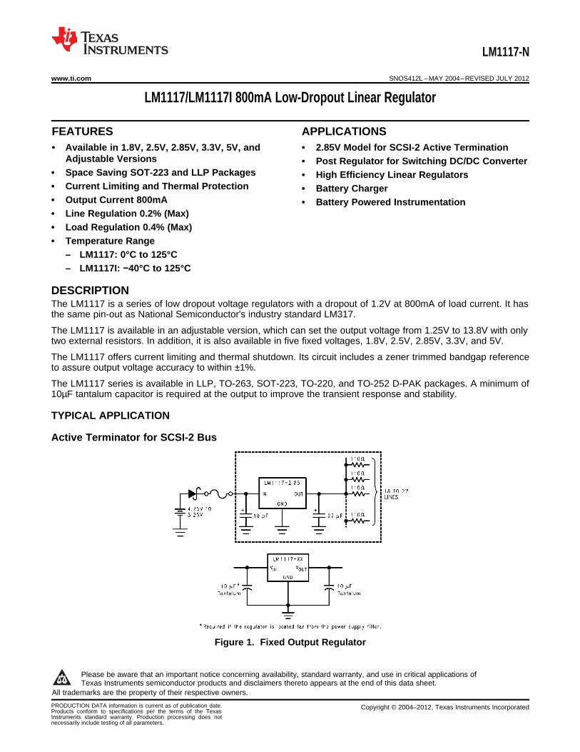
TYPICAL APPLICATION
Active Terminator for SCSI-2 Bus
Figure 1. Fixed Output Regulator
1
Please be aware that an important notice concerning availability, standard warranty, and use in critical applications ofTexas Instruments semiconductor products and disclaimers thereto appears at the end of this data sheet.
2All trademarks are the property of their respective owners.
PRODUCTION DATA information is current as of publication date. Copyright © 2004–2012, Texas Instruments IncorporatedProducts conform to specifications per the terms of the TexasInstruments standard warranty. Production processing does notnecessarily include testing of all parameters.
LM1117-N
SNOS412L –MAY 2004–REVISED JULY 2012 www.ti.com
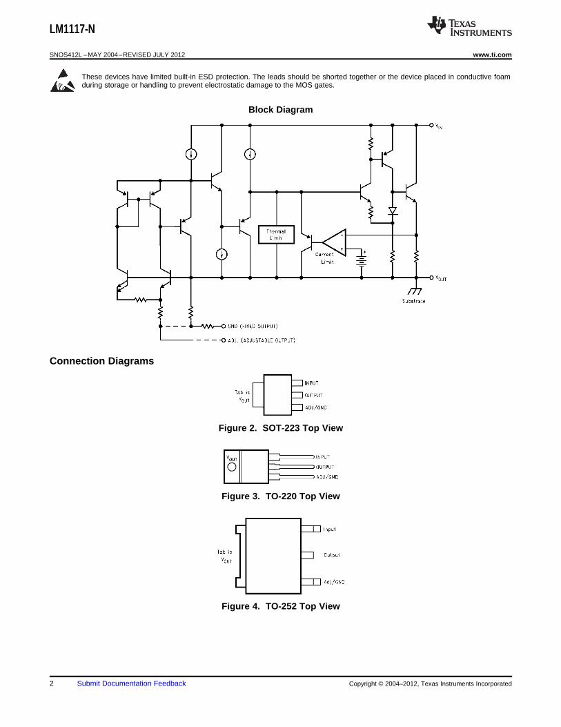
These devices have limited built-in ESD protection. The leads should be shorted together or the device placed in conductive foamduring storage or handling to prevent electrostatic damage to the MOS gates.
Block Diagram
Connection Diagrams
Figure 2. SOT-223 Top View
Figure 3. TO-220 Top View
Figure 4. TO-252 Top View
2 Submit Documentation Feedback Copyright © 2004–2012, Texas Instruments Incorporated
NOT CONNECTED
VOUT
VOUT
VOUT
1
2
3
4
8
7
6
5
ADJ/GND
VIN
VIN
VIN
VOUT
LM1117-N
www.ti.com SNOS412L –MAY 2004–REVISED JULY 2012
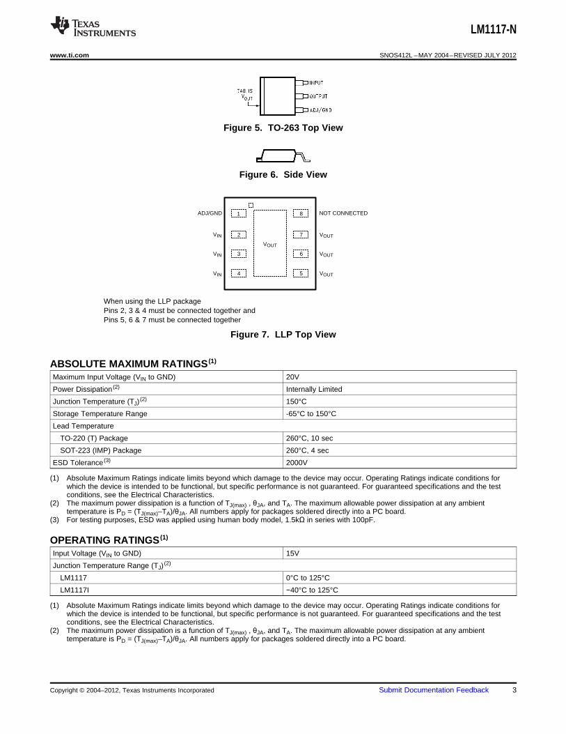
Figure 5. TO-263 Top View
Figure 6. Side View
When using the LLP packagePins 2, 3 & 4 must be connected together andPins 5, 6 & 7 must be connected together
Figure 7. LLP Top View
ABSOLUTE MAXIMUM RATINGS (1)
Maximum Input Voltage (VIN to GND) 20V
Power Dissipation (2) Internally Limited
Junction Temperature (TJ)(2) 150°C
Storage Temperature Range -65°C to 150°C
Lead Temperature
TO-220 (T) Package 260°C, 10 sec
SOT-223 (IMP) Package 260°C, 4 sec
ESD Tolerance (3) 2000V
(1) Absolute Maximum Ratings indicate limits beyond which damage to the device may occur. Operating Ratings indicate conditions forwhich the device is intended to be functional, but specific performance is not guaranteed. For guaranteed specifications and the testconditions, see the Electrical Characteristics.
(2) The maximum power dissipation is a function of TJ(max) , θJA, and TA. The maximum allowable power dissipation at any ambienttemperature is PD = (TJ(max)–TA)/θJA. All numbers apply for packages soldered directly into a PC board.
(3) For testing purposes, ESD was applied using human body model, 1.5kΩ in series with 100pF.
OPERATING RATINGS (1)
Input Voltage (VIN to GND) 15V
Junction Temperature Range (TJ)(2)
LM1117 0°C to 125°C
LM1117I −40°C to 125°C
(1) Absolute Maximum Ratings indicate limits beyond which damage to the device may occur. Operating Ratings indicate conditions forwhich the device is intended to be functional, but specific performance is not guaranteed. For guaranteed specifications and the testconditions, see the Electrical Characteristics.
(2) The maximum power dissipation is a function of TJ(max) , θJA, and TA. The maximum allowable power dissipation at any ambienttemperature is PD = (TJ(max)–TA)/θJA. All numbers apply for packages soldered directly into a PC board.
Copyright © 2004–2012, Texas Instruments Incorporated Submit Documentation Feedback 3
LM1117-N
SNOS412L –MAY 2004–REVISED JULY 2012 www.ti.com
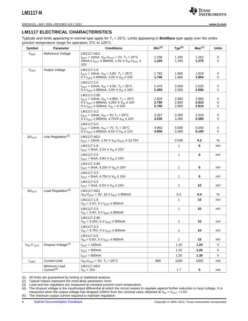
LM1117 ELECTRICAL CHARACTERISTICSTypicals and limits appearing in normal type apply for TJ = 25°C. Limits appearing in Boldface type apply over the entirejunction temperature range for operation, 0°C to 125°C.
Symbol Parameter Conditions Min (1) Typ (2) Max (1) Units
VREF Reference Voltage LM1117-ADJIOUT = 10mA, VIN-VOUT = 2V, TJ = 25°C 1.238 1.250 1.262 V10mA ≤ IOUT ≤ 800mA, 1.4V ≤ VIN-VOUT ≤ 1.225 1.250 1.270 V10V
VOUT Output Voltage LM1117-1.8IOUT = 10mA, VIN = 3.8V, TJ = 25°C 1.782 1.800 1.818 V0 ≤ IOUT ≤ 800mA, 3.2V ≤ VIN ≤ 10V 1.746 1.800 1.854 V
LM1117-2.5IOUT = 10mA, VIN = 4.5V, TJ = 25°C 2.475 2.500 2.525 V0 ≤ IOUT ≤ 800mA, 3.9V ≤ VIN ≤ 10V 2.450 2.500 2.550 V
LM1117-2.85IOUT = 10mA, VIN = 4.85V, TJ = 25°C 2.820 2.850 2.880 V0 ≤ IOUT ≤ 800mA, 4.25V ≤ VIN ≤ 10V 2.790 2.850 2.910 V0 ≤ IOUT ≤ 500mA, VIN = 4.10V 2.790 2.850 2.910 V
LM1117-3.3IOUT = 10mA, VIN = 5V TJ = 25°C 3.267 3.300 3.333 V0 ≤ IOUT ≤ 800mA, 4.75V≤ VIN ≤ 10V 3.235 3.300 3.365 V
LM1117-5.0IOUT = 10mA, VIN = 7V, TJ = 25°C 4.950 5.000 5.050 V0 ≤ IOUT ≤ 800mA, 6.5V ≤ VIN ≤ 12V 4.900 5.000 5.100 V
ΔVOUT Line Regulation (3) LM1117-ADJIOUT = 10mA, 1.5V ≤ VIN-VOUT ≤ 13.75V 0.035 0.2 %
LM1117-1.8 1 6 mVIOUT = 0mA, 3.2V ≤ VIN ≤ 10V
LM1117-2.5 1 6 mVIOUT = 0mA, 3.9V ≤ VIN ≤ 10V
LM1117-2.85IOUT = 0mA, 4.25V ≤ VIN ≤ 10V 1 6 mV
LM1117-3.3IOUT = 0mA, 4.75V ≤ VIN ≤ 15V 1 6 mV
LM1117-5.0IOUT = 0mA, 6.5V ≤ VIN ≤ 15V 1 10 mV
ΔVOUT Load Regulation (3) LM1117-ADJVIN-VOUT = 3V, 10 ≤ IOUT ≤ 800mA 0.2 0.4 %
LM1117-1.8 1 10 mVVIN = 3.2V, 0 ≤ IOUT ≤ 800mA
LM1117-2.5 1 10 mVVIN = 3.9V, 0 ≤ IOUT ≤ 800mA
LM1117-2.85VIN = 4.25V, 0 ≤ IOUT ≤ 800mA 1 10 mV
LM1117-3.3VIN = 4.75V, 0 ≤ IOUT ≤ 800mA 1 10 mV
LM1117-5.0VIN = 6.5V, 0 ≤ IOUT ≤ 800mA 1 15 mV
VIN-V OUT Dropout Voltage (4) IOUT = 100mA 1.10 1.20 V
IOUT = 500mA 1.15 1.25 V
IOUT = 800mA 1.20 1.30 V
ILIMIT Current Limit VIN-VOUT = 5V, TJ = 25°C 800 1200 1500 mA
Minimum Load LM1117-ADJCurrent (5) VIN = 15V 1.7 5 mA
(1) All limits are guaranteed by testing or statistical analysis.(2) Typical Values represent the most likely parametric norm.(3) Load and line regulation are measured at constant junction room temperature.(4) The dropout voltage is the input/output differential at which the circuit ceases to regulate against further reduction in input voltage. It is
measured when the output voltage has dropped 100mV from the nominal value obtained at VIN = VOUT +1.5V.(5) The minimum output current required to maintain regulation.
4 Submit Documentation Feedback Copyright © 2004–2012, Texas Instruments Incorporated
LM1117-N
www.ti.com SNOS412L –MAY 2004–REVISED JULY 2012
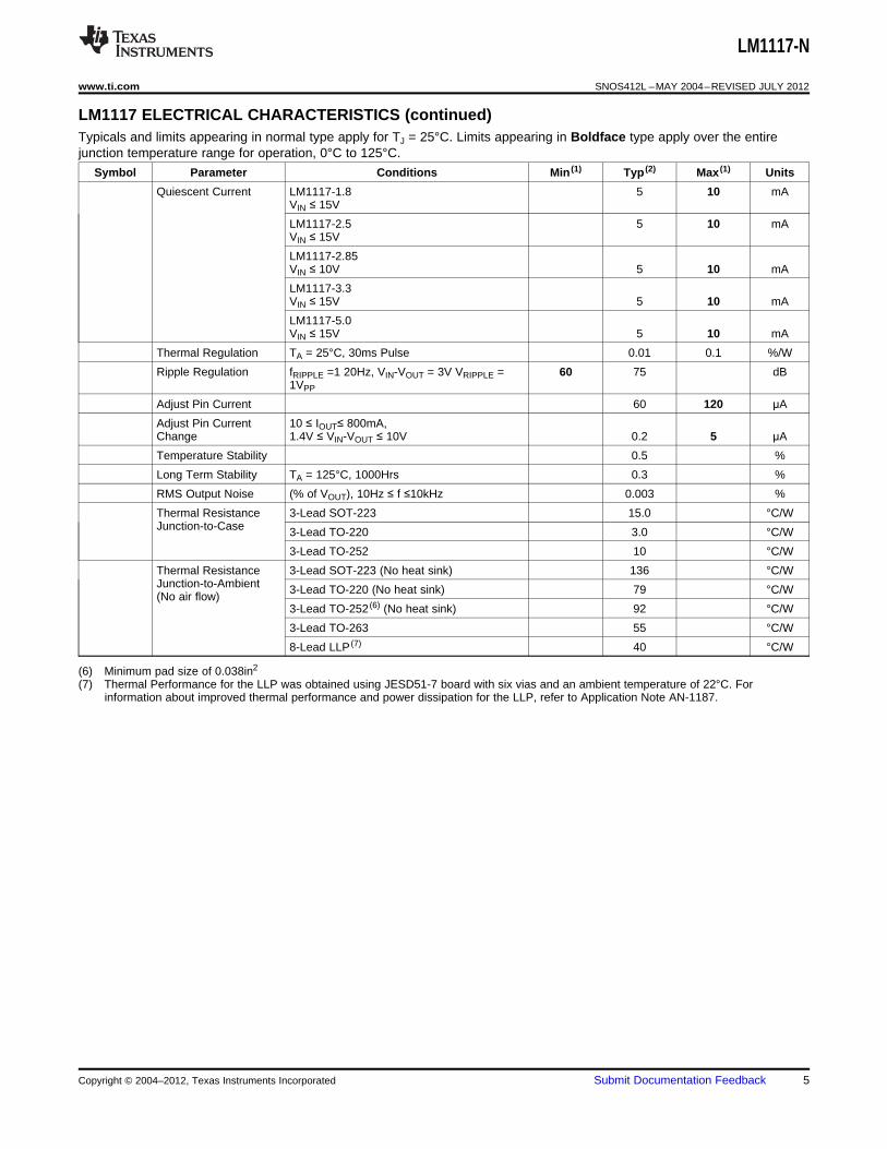
LM1117 ELECTRICAL CHARACTERISTICS (continued)Typicals and limits appearing in normal type apply for TJ = 25°C. Limits appearing in Boldface type apply over the entirejunction temperature range for operation, 0°C to 125°C.
Symbol Parameter Conditions Min (1) Typ (2) Max (1) Units
Quiescent Current LM1117-1.8 5 10 mAVIN ≤ 15V
LM1117-2.5 5 10 mAVIN ≤ 15V
LM1117-2.85VIN ≤ 10V 5 10 mA
LM1117-3.3VIN ≤ 15V 5 10 mA
LM1117-5.0VIN ≤ 15V 5 10 mA
Thermal Regulation TA = 25°C, 30ms Pulse 0.01 0.1 %/W
Ripple Regulation fRIPPLE =1 20Hz, VIN-VOUT = 3V VRIPPLE = 60 75 dB1VPP
Adjust Pin Current 60 120 μA
Adjust Pin Current 10 ≤ IOUT≤ 800mA,Change 1.4V ≤ VIN-VOUT ≤ 10V 0.2 5 μA
Temperature Stability 0.5 %
Long Term Stability TA = 125°C, 1000Hrs 0.3 %
RMS Output Noise (% of VOUT), 10Hz ≤ f ≤10kHz 0.003 %
Thermal Resistance 3-Lead SOT-223 15.0 °C/WJunction-to-Case 3-Lead TO-220 3.0 °C/W
3-Lead TO-252 10 °C/W
Thermal Resistance 3-Lead SOT-223 (No heat sink) 136 °C/WJunction-to-Ambient 3-Lead TO-220 (No heat sink) 79 °C/W(No air flow)
3-Lead TO-252 (6) (No heat sink) 92 °C/W
3-Lead TO-263 55 °C/W
8-Lead LLP (7) 40 °C/W
(6) Minimum pad size of 0.038in2
(7) Thermal Performance for the LLP was obtained using JESD51-7 board with six vias and an ambient temperature of 22°C. Forinformation about improved thermal performance and power dissipation for the LLP, refer to Application Note AN-1187.
Copyright © 2004–2012, Texas Instruments Incorporated Submit Documentation Feedback 5
LM1117-N
SNOS412L –MAY 2004–REVISED JULY 2012 www.ti.com
LM1117I ELECTRICAL CHARACTERISTICSTypicals and limits appearing in normal type apply for TJ = 25°C. Limits appearing in Boldface type apply over the entirejunction temperature range for operation, −40°C to 125°C.
Symbol Parameter Conditions Min (1) Typ (2) Max (1) Units
VREF Reference Voltage LM1117I-ADJIOUT = 10mA, VIN-VOUT = 2V, TJ = 25°C 1.238 1.250 1.262 V10mA ≤ IOUT ≤ 800mA, 1.4V ≤ VIN-VOUT ≤ 1.200 1.250 1.290 V10V
VOUT Output Voltage LM1117I-3.3IOUT = 10mA, VIN = 5V, TJ = 25°C 3.267 3.300 3.333 V0 ≤ IOUT ≤ 800mA, 4.75V ≤ VIN ≤ 10V 3.168 3.300 3.432 V
LM1117I-5.0IOUT = 10mA, VIN = 7V, TJ = 25°C 4.950 5.000 5.050 V0 ≤ IOUT ≤ 800mA, 6.5V ≤ VIN ≤ 12V 4.800 5.000 5.200 V
ΔVOUT Line Regulation (3) LM1117I-ADJIOUT = 10mA, 1.5V ≤ VIN-VOUT ≤ 13.75V 0.035 0.3 %
LM1117I-3.3IOUT = 0mA, 4.75V ≤ VIN ≤ 15V 1 10 mV
LM1117I-5.0IOUT = 0mA, 6.5V ≤ VIN ≤ 15V 1 15 mV
ΔVOUT Load Regulation (3) LM1117I-ADJVIN-VOUT = 3V, 10 ≤ IOUT ≤ 800mA 0.2 0.5 %
LM1117I-3.3VIN = 4.75V, 0 ≤ IOUT ≤ 800mA 1 15 mV
LM1117I-5.0VIN = 6.5V, 0 ≤ IOUT ≤ 800mA 1 20 mV
VIN-V OUT Dropout Voltage (4) IOUT = 100mA 1.10 1.30 V
IOUT = 500mA 1.15 1.35 V
IOUT = 800mA 1.20 1.40 V
ILIMIT Current Limit VIN-VOUT = 5V, TJ = 25°C 800 1200 1500 mA
Minimum Load LM1117I-ADJCurrent (5) VIN = 15V 1.7 5 mA
Quiescent Current LM1117I-3.3VIN ≤ 15V 5 15 mA
LM1117I-5.0VIN ≤ 15V 5 15 mA
Thermal Regulation TA = 25°C, 30ms Pulse 0.01 0.1 %/W
Ripple Regulation fRIPPLE =1 20Hz, VIN-VOUT = 3V VRIPPLE = 60 75 dB1VPP
Adjust Pin Current 60 120 μA
Adjust Pin Current 10 ≤ IOUT≤ 800mA,Change 1.4V ≤ VIN-VOUT ≤ 10V 0.2 10 μA
Temperature Stability 0.5 %
Long Term Stability TA = 125°C, 1000Hrs 0.3 %
RMS Output Noise (% of VOUT), 10Hz ≤ f ≤10kHz 0.003 %
Thermal Resistance 3-Lead SOT-223 15.0 °C/WJunction-to-Case 3-Lead TO-252 10 °C/W
(1) All limits are guaranteed by testing or statistical analysis.(2) Typical Values represent the most likely parametric norm.(3) Load and line regulation are measured at constant junction room temperature.(4) The dropout voltage is the input/output differential at which the circuit ceases to regulate against further reduction in input voltage. It is
measured when the output voltage has dropped 100mV from the nominal value obtained at VIN = VOUT +1.5V.(5) The minimum output current required to maintain regulation.
6 Submit Documentation Feedback Copyright © 2004–2012, Texas Instruments Incorporated
LM1117-N
www.ti.com SNOS412L –MAY 2004–REVISED JULY 2012
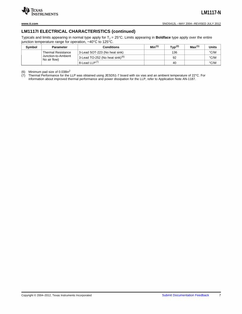
LM1117I ELECTRICAL CHARACTERISTICS (continued)Typicals and limits appearing in normal type apply for TJ = 25°C. Limits appearing in Boldface type apply over the entirejunction temperature range for operation, −40°C to 125°C.
Symbol Parameter Conditions Min (1) Typ (2) Max (1) Units
Thermal Resistance 3-Lead SOT-223 (No heat sink) 136 °C/WJunction-to-Ambient 3-Lead TO-252 (No heat sink) (6) 92 °C/WNo air flow)
8-Lead LLP (7) 40 °C/W
(6) Minimum pad size of 0.038in2
(7) Thermal Performance for the LLP was obtained using JESD51-7 board with six vias and an ambient temperature of 22°C. Forinformation about improved thermal performance and power dissipation for the LLP, refer to Application Note AN-1187.
Copyright © 2004–2012, Texas Instruments Incorporated Submit Documentation Feedback 7
LM1117-N
SNOS412L –MAY 2004–REVISED JULY 2012 www.ti.com
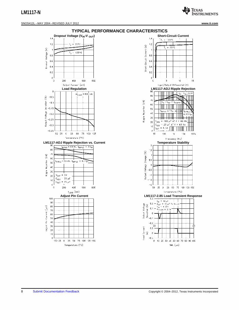
TYPICAL PERFORMANCE CHARACTERISTICSDropout Voltage (VIN-V OUT) Short-Circuit Current
Load Regulation LM1117-ADJ Ripple Rejection
LM1117-ADJ Ripple Rejection vs. Current Temperature Stability
Adjust Pin Current LM1117-2.85 Load Transient Response
8 Submit Documentation Feedback Copyright © 2004–2012, Texas Instruments Incorporated
LM1117-N
www.ti.com SNOS412L –MAY 2004–REVISED JULY 2012
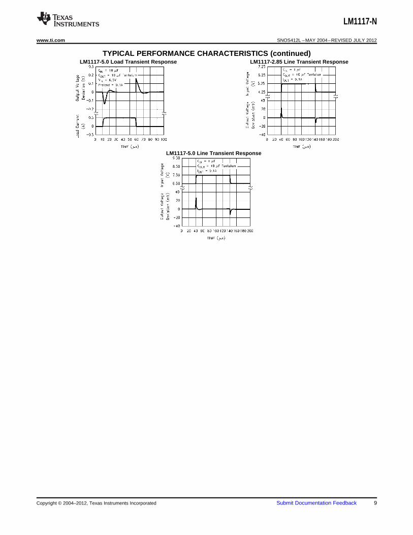
TYPICAL PERFORMANCE CHARACTERISTICS (continued)LM1117-5.0 Load Transient Response LM1117-2.85 Line Transient Response
LM1117-5.0 Line Transient Response
Copyright © 2004–2012, Texas Instruments Incorporated Submit Documentation Feedback 9
LM1117-N
SNOS412L –MAY 2004–REVISED JULY 2012 www.ti.com
APPLICATION INFORMATION
EXTERNAL CAPACITORS/STABILITY
Input Bypass Capacitor
An input capacitor is recommended. A 10µF tantalum on the input is a suitable input bypassing for almost allapplications.
Adjust Terminal Bypass Capacitor
The adjust terminal can be bypassed to ground with a bypass capacitor (CADJ) to improve ripple rejection. Thisbypass capacitor prevents ripple from being amplified as the output voltage is increased. At any ripple frequency,the impedance of the CADJ should be less than R1 to prevent the ripple from being amplified:
1/(2π*fRIPPLE*CADJ) < R1
The R1 is the resistor between the output and the adjust pin. Its value is normally in the range of 100-200Ω. Forexample, with R1 = 124Ω and fRIPPLE = 120Hz, the CADJ should be > 11µF.
Output Capacitor
The output capacitor is critical in maintaining regulator stability, and must meet the required conditions for bothminimum amount of capacitance and ESR (Equivalent Series Resistance). The minimum output capacitancerequired by the LM1117 is 10µF, if a tantalum capacitor is used. Any increase of the output capacitance willmerely improve the loop stability and transient response. The ESR of the output capacitor should range between0.3Ω - 22Ω. In the case of the adjustable regulator, when the CADJ is used, a larger output capacitance (22µftantalum) is required.
OUTPUT VOLTAGE
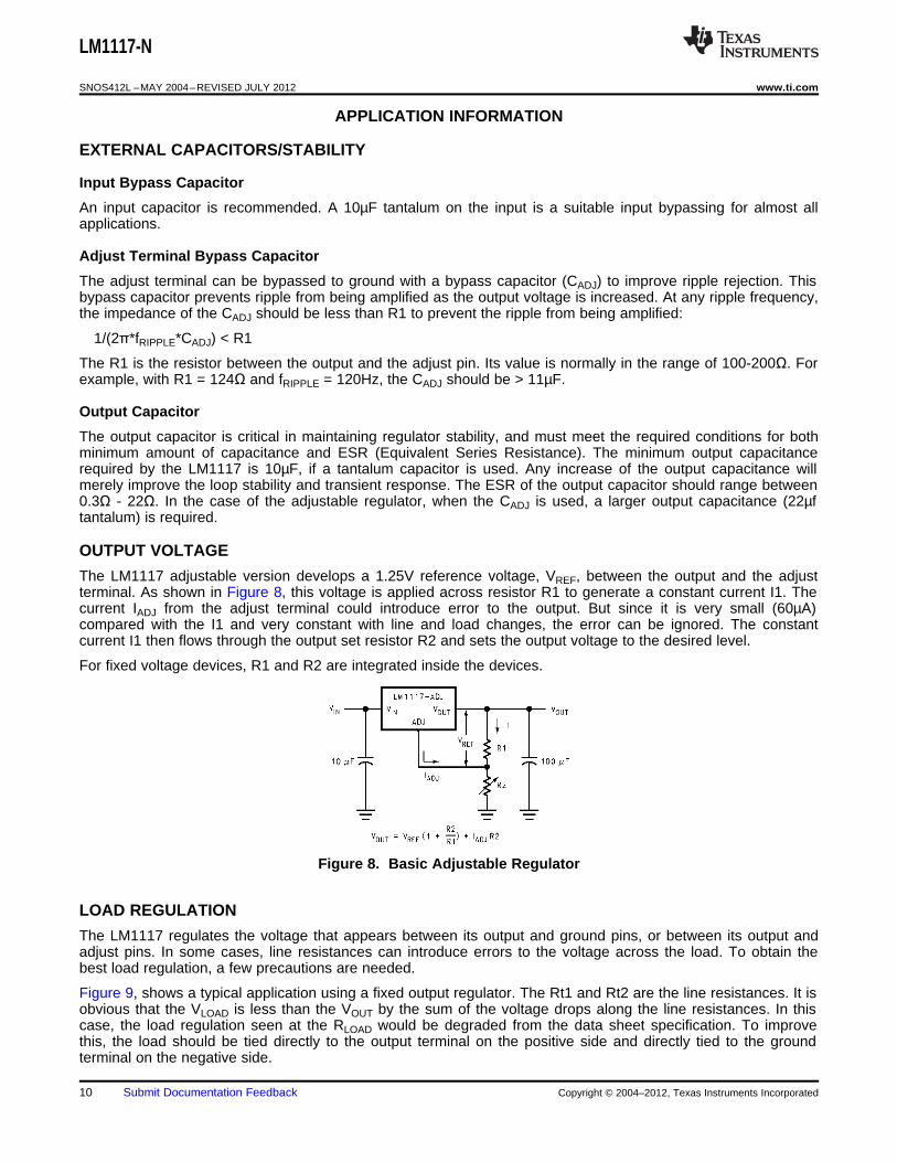
The LM1117 adjustable version develops a 1.25V reference voltage, VREF, between the output and the adjustterminal. As shown in Figure 8, this voltage is applied across resistor R1 to generate a constant current I1. Thecurrent IADJ from the adjust terminal could introduce error to the output. But since it is very small (60µA)compared with the I1 and very constant with line and load changes, the error can be ignored. The constantcurrent I1 then flows through the output set resistor R2 and sets the output voltage to the desired level.
For fixed voltage devices, R1 and R2 are integrated inside the devices.
Figure 8. Basic Adjustable Regulator
LOAD REGULATION
The LM1117 regulates the voltage that appears between its output and ground pins, or between its output andadjust pins. In some cases, line resistances can introduce errors to the voltage across the load. To obtain thebest load regulation, a few precautions are needed.
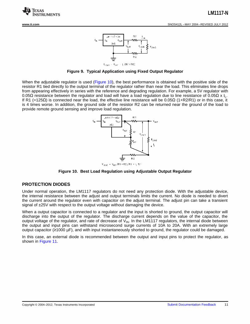
Figure 9, shows a typical application using a fixed output regulator. The Rt1 and Rt2 are the line resistances. It isobvious that the VLOAD is less than the VOUT by the sum of the voltage drops along the line resistances. In thiscase, the load regulation seen at the RLOAD would be degraded from the data sheet specification. To improvethis, the load should be tied directly to the output terminal on the positive side and directly tied to the groundterminal on the negative side.
10 Submit Documentation Feedback Copyright © 2004–2012, Texas Instruments Incorporated
LM1117-N
www.ti.com SNOS412L –MAY 2004–REVISED JULY 2012
Figure 9. Typical Application using Fixed Output Regulator
When the adjustable regulator is used (Figure 10), the best performance is obtained with the positive side of theresistor R1 tied directly to the output terminal of the regulator rather than near the load. This eliminates line dropsfrom appearing effectively in series with the reference and degrading regulation. For example, a 5V regulator with0.05Ω resistance between the regulator and load will have a load regulation due to line resistance of 0.05Ω x IL.If R1 (=125Ω) is connected near the load, the effective line resistance will be 0.05Ω (1+R2/R1) or in this case, itis 4 times worse. In addition, the ground side of the resistor R2 can be returned near the ground of the load toprovide remote ground sensing and improve load regulation.
Figure 10. Best Load Regulation using Adjustable Output Regulator
PROTECTION DIODES
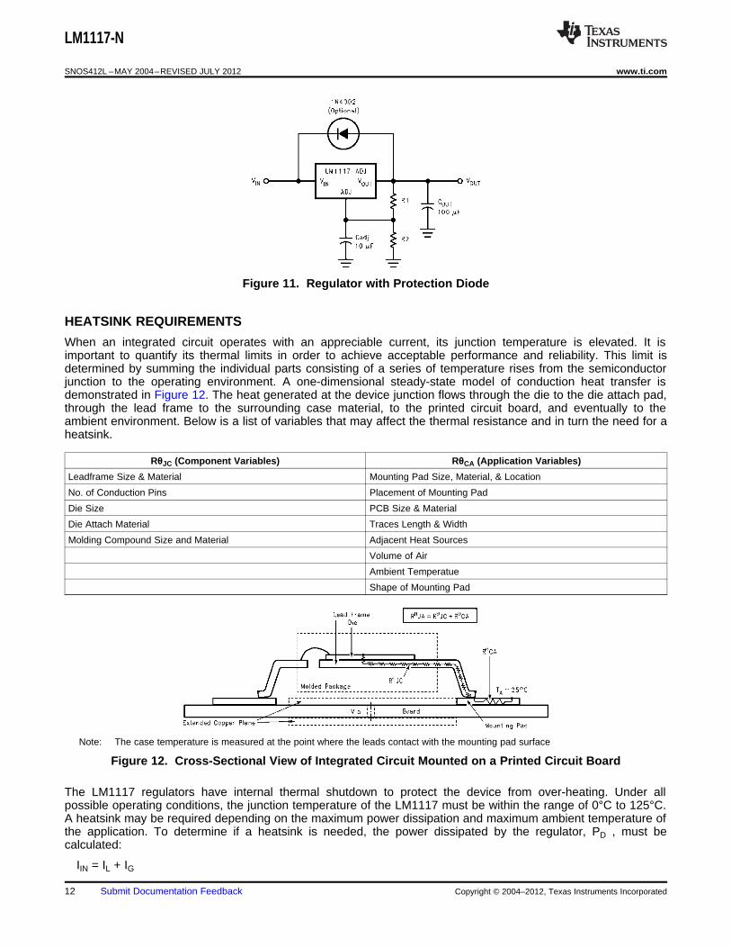
Under normal operation, the LM1117 regulators do not need any protection diode. With the adjustable device,the internal resistance between the adjust and output terminals limits the current. No diode is needed to divertthe current around the regulator even with capacitor on the adjust terminal. The adjust pin can take a transientsignal of ±25V with respect to the output voltage without damaging the device.
When a output capacitor is connected to a regulator and the input is shorted to ground, the output capacitor willdischarge into the output of the regulator. The discharge current depends on the value of the capacitor, theoutput voltage of the regulator, and rate of decrease of VIN. In the LM1117 regulators, the internal diode betweenthe output and input pins can withstand microsecond surge currents of 10A to 20A. With an extremely largeoutput capacitor (≥1000 µF), and with input instantaneously shorted to ground, the regulator could be damaged.
In this case, an external diode is recommended between the output and input pins to protect the regulator, asshown in Figure 11.
Copyright © 2004–2012, Texas Instruments Incorporated Submit Documentation Feedback 11
LM1117-N
SNOS412L –MAY 2004–REVISED JULY 2012 www.ti.com
Figure 11. Regulator with Protection Diode
HEATSINK REQUIREMENTS
When an integrated circuit operates with an appreciable current, its junction temperature is elevated. It isimportant to quantify its thermal limits in order to achieve acceptable performance and reliability. This limit isdetermined by summing the individual parts consisting of a series of temperature rises from the semiconductorjunction to the operating environment. A one-dimensional steady-state model of conduction heat transfer isdemonstrated in Figure 12. The heat generated at the device junction flows through the die to the die attach pad,through the lead frame to the surrounding case material, to the printed circuit board, and eventually to theambient environment. Below is a list of variables that may affect the thermal resistance and in turn the need for aheatsink.
RθJC (Component Variables) RθCA (Application Variables)
Leadframe Size & Material Mounting Pad Size, Material, & Location
No. of Conduction Pins Placement of Mounting Pad
Die Size PCB Size & Material
Die Attach Material Traces Length & Width
Molding Compound Size and Material Adjacent Heat Sources
Volume of Air
Ambient Temperatue
Shape of Mounting Pad
Note: The case temperature is measured at the point where the leads contact with the mounting pad surface
Figure 12. Cross-Sectional View of Integrated Circuit Mounted on a Printed Circuit Board
The LM1117 regulators have internal thermal shutdown to protect the device from over-heating. Under allpossible operating conditions, the junction temperature of the LM1117 must be within the range of 0°C to 125°C.A heatsink may be required depending on the maximum power dissipation and maximum ambient temperature ofthe application. To determine if a heatsink is needed, the power dissipated by the regulator, PD , must becalculated:
IIN = IL + IG
12 Submit Documentation Feedback Copyright © 2004–2012, Texas Instruments Incorporated
LM1117-N
www.ti.com SNOS412L –MAY 2004–REVISED JULY 2012
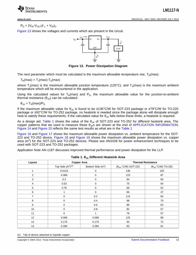
PD = (VIN-VOUT)I L + VINIG
Figure 13 shows the voltages and currents which are present in the circuit.
Figure 13. Power Dissipation Diagram
The next parameter which must be calculated is the maximum allowable temperature rise, TR(max):
TR(max) = TJ(max)-TA(max)
where TJ(max) is the maximum allowable junction temperature (125°C), and TA(max) is the maximum ambienttemperature which will be encountered in the application.
Using the calculated values for TR(max) and PD, the maximum allowable value for the junction-to-ambientthermal resistance (θJA) can be calculated:
θJA = TR(max)/PD
If the maximum allowable value for θJA is found to be ≥136°C/W for SOT-223 package or ≥79°C/W for TO-220package or ≥92°C/W for TO-252 package, no heatsink is needed since the package alone will dissipate enoughheat to satisfy these requirements. If the calculated value for θJA falls below these limits, a heatsink is required.
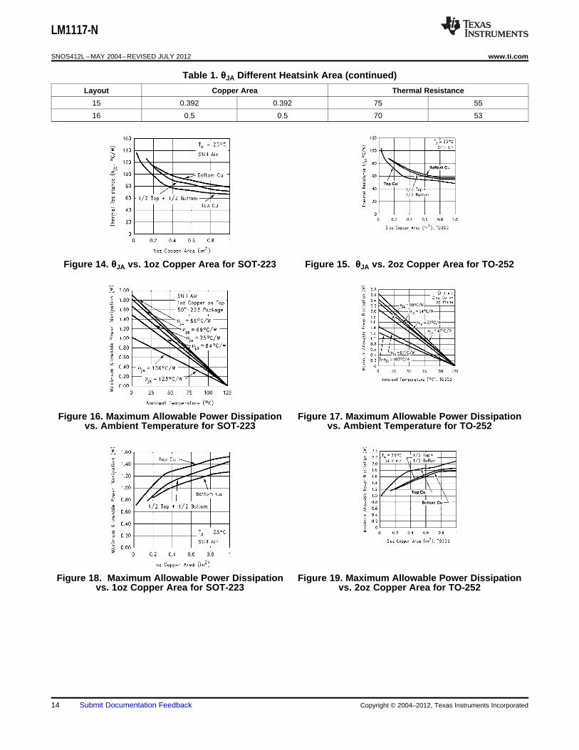
As a design aid, Table 1 shows the value of the θJA of SOT-223 and TO-252 for different heatsink area. Thecopper patterns that we used to measure these θJAs are shown at the end of APPLICATION INFORMATION.Figure 14 and Figure 15 reflects the same test results as what are in the Table 1
Figure 16 and Figure 17 shows the maximum allowable power dissipation vs. ambient temperature for the SOT-223 and TO-252 device. Figure 18 and Figure 19 shows the maximum allowable power dissipation vs. copperarea (in2) for the SOT-223 and TO-252 devices. Please see AN1028 for power enhancement techniques to beused with SOT-223 and TO-252 packages.
Application Note AN-1187 discusses improved thermal performance and power dissipation for the LLP.
Table 1. θJA Different Heatsink Area
Layout Copper Area Thermal Resistance
Top Side (in2) (1) Bottom Side (in2) (θJA,°C/W) SOT-223 (θJA,°C/W) TO-252
1 0.0123 0 136 103
2 0.066 0 123 87
3 0.3 0 84 60
4 0.53 0 75 54
5 0.76 0 69 52
6 1 0 66 47
7 0 0.2 115 84
8 0 0.4 98 70
9 0 0.6 89 63
10 0 0.8 82 57
11 0 1 79 57
12 0.066 0.066 125 89
13 0.175 0.175 93 72
14 0.284 0.284 83 61
(1) Tab of device attached to topside copper
Copyright © 2004–2012, Texas Instruments Incorporated Submit Documentation Feedback 13
LM1117-N
SNOS412L –MAY 2004–REVISED JULY 2012 www.ti.com
Table 1. θJA Different Heatsink Area (continued)
Layout Copper Area Thermal Resistance
15 0.392 0.392 75 55
16 0.5 0.5 70 53
Figure 14. θJA vs. 1oz Copper Area for SOT-223 Figure 15. θJA vs. 2oz Copper Area for TO-252
Figure 16. Maximum Allowable Power Dissipation Figure 17. Maximum Allowable Power Dissipationvs. Ambient Temperature for SOT-223 vs. Ambient Temperature for TO-252
Figure 18. Maximum Allowable Power Dissipation Figure 19. Maximum Allowable Power Dissipationvs. 1oz Copper Area for SOT-223 vs. 2oz Copper Area for TO-252
14 Submit Documentation Feedback Copyright © 2004–2012, Texas Instruments Incorporated
LM1117-N
www.ti.com SNOS412L –MAY 2004–REVISED JULY 2012
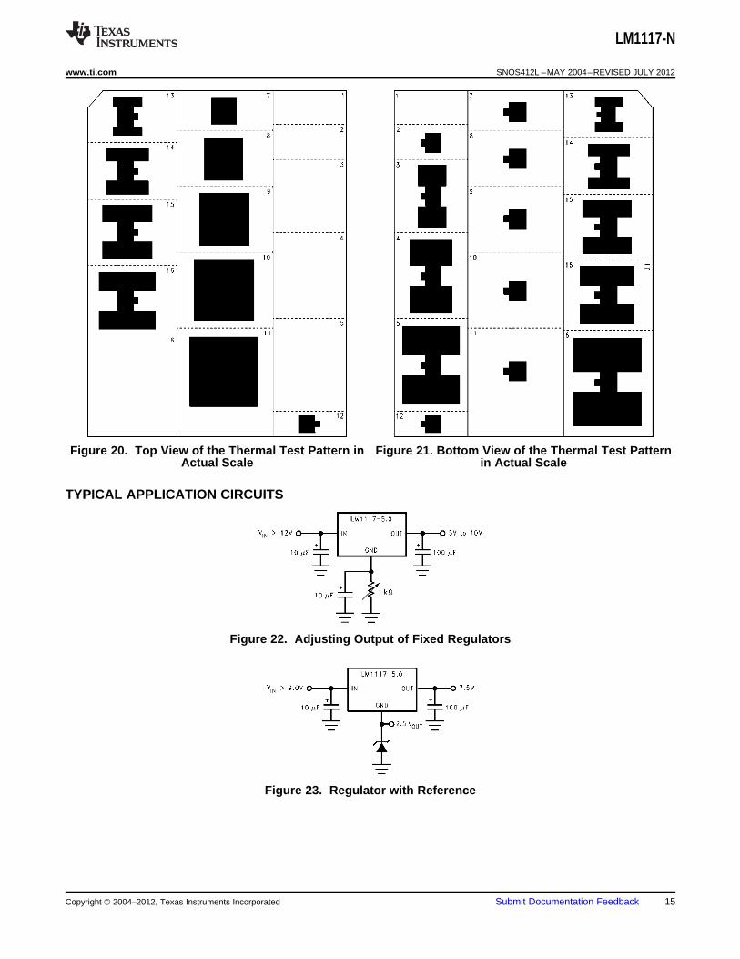
Figure 20. Top View of the Thermal Test Pattern in Figure 21. Bottom View of the Thermal Test PatternActual Scale in Actual Scale
TYPICAL APPLICATION CIRCUITS
Figure 22. Adjusting Output of Fixed Regulators
Figure 23. Regulator with Reference
Copyright © 2004–2012, Texas Instruments Incorporated Submit Documentation Feedback 15
LM1117-N
SNOS412L –MAY 2004–REVISED JULY 2012 www.ti.com
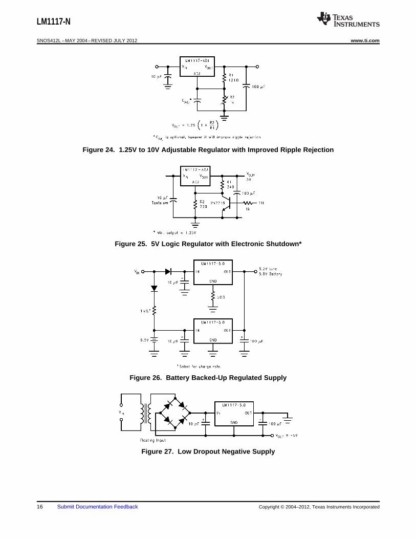
Figure 24. 1.25V to 10V Adjustable Regulator with Improved Ripple Rejection
Figure 25. 5V Logic Regulator with Electronic Shutdown*
Figure 26. Battery Backed-Up Regulated Supply
Figure 27. Low Dropout Negative Supply
16 Submit Documentation Feedback Copyright © 2004–2012, Texas Instruments Incorporated
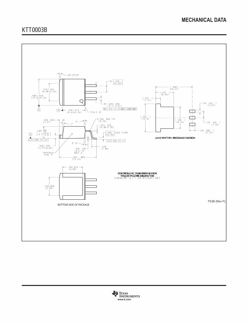
MECHANICAL DATA
KTT0003B
www.ti.com
BOTTOM SIDE OF PACKAGETS3B (Rev F)
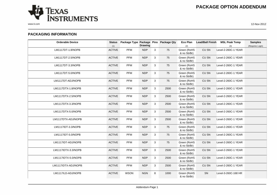
PACKAGE OPTION ADDENDUM
www.ti.com 12-Nov-2012
Addendum-Page 1
PACKAGING INFORMATION
Orderable Device Status(1)
Package Type PackageDrawing
Pins Package Qty Eco Plan(2)
Lead/Ball Finish MSL Peak Temp(3)
Samples(Requires Login)
LM1117DT-1.8/NOPB ACTIVE PFM NDP 3 75 Green (RoHS& no Sb/Br)
CU SN Level-2-260C-1 YEAR
LM1117DT-2.5/NOPB ACTIVE PFM NDP 3 75 Green (RoHS& no Sb/Br)
CU SN Level-2-260C-1 YEAR
LM1117DT-3.3/NOPB ACTIVE PFM NDP 3 75 Green (RoHS& no Sb/Br)
CU SN Level-2-260C-1 YEAR
LM1117DT-5.0/NOPB ACTIVE PFM NDP 3 75 Green (RoHS& no Sb/Br)
CU SN Level-2-260C-1 YEAR
LM1117DT-ADJ/NOPB ACTIVE PFM NDP 3 75 Green (RoHS& no Sb/Br)
CU SN Level-2-260C-1 YEAR
LM1117DTX-1.8/NOPB ACTIVE PFM NDP 3 2500 Green (RoHS& no Sb/Br)
CU SN Level-2-260C-1 YEAR
LM1117DTX-2.5/NOPB ACTIVE PFM NDP 3 2500 Green (RoHS& no Sb/Br)
CU SN Level-2-260C-1 YEAR
LM1117DTX-3.3/NOPB ACTIVE PFM NDP 3 2500 Green (RoHS& no Sb/Br)
CU SN Level-2-260C-1 YEAR
LM1117DTX-5.0/NOPB ACTIVE PFM NDP 3 2500 Green (RoHS& no Sb/Br)
CU SN Level-2-260C-1 YEAR
LM1117DTX-ADJ/NOPB ACTIVE PFM NDP 3 2500 Green (RoHS& no Sb/Br)
CU SN Level-2-260C-1 YEAR
LM1117IDT-3.3/NOPB ACTIVE PFM NDP 3 75 Green (RoHS& no Sb/Br)
CU SN Level-2-260C-1 YEAR
LM1117IDT-5.0/NOPB ACTIVE PFM NDP 3 75 Green (RoHS& no Sb/Br)
CU SN Level-2-260C-1 YEAR
LM1117IDT-ADJ/NOPB ACTIVE PFM NDP 3 75 Green (RoHS& no Sb/Br)
CU SN Level-2-260C-1 YEAR
LM1117IDTX-3.3/NOPB ACTIVE PFM NDP 3 2500 Green (RoHS& no Sb/Br)
CU SN Level-2-260C-1 YEAR
LM1117IDTX-5.0/NOPB ACTIVE PFM NDP 3 2500 Green (RoHS& no Sb/Br)
CU SN Level-2-260C-1 YEAR
LM1117IDTX-ADJ/NOPB ACTIVE PFM NDP 3 2500 Green (RoHS& no Sb/Br)
CU SN Level-2-260C-1 YEAR
LM1117ILD-ADJ/NOPB ACTIVE WSON NGN 8 1000 Green (RoHS& no Sb/Br)
SN Level-3-260C-168 HR
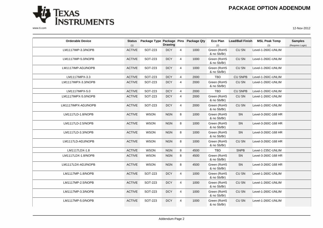
PACKAGE OPTION ADDENDUM
www.ti.com 12-Nov-2012
Addendum-Page 2
Orderable Device Status(1)
Package Type PackageDrawing
Pins Package Qty Eco Plan(2)
Lead/Ball Finish MSL Peak Temp(3)
Samples(Requires Login)
LM1117IMP-3.3/NOPB ACTIVE SOT-223 DCY 4 1000 Green (RoHS& no Sb/Br)
CU SN Level-1-260C-UNLIM
LM1117IMP-5.0/NOPB ACTIVE SOT-223 DCY 4 1000 Green (RoHS& no Sb/Br)
CU SN Level-1-260C-UNLIM
LM1117IMP-ADJ/NOPB ACTIVE SOT-223 DCY 4 1000 Green (RoHS& no Sb/Br)
CU SN Level-1-260C-UNLIM
LM1117IMPX-3.3 ACTIVE SOT-223 DCY 4 2000 TBD CU SNPB Level-1-260C-UNLIM
LM1117IMPX-3.3/NOPB ACTIVE SOT-223 DCY 4 2000 Green (RoHS& no Sb/Br)
CU SN Level-1-260C-UNLIM
LM1117IMPX-5.0 ACTIVE SOT-223 DCY 4 2000 TBD CU SNPB Level-1-260C-UNLIM
LM1117IMPX-5.0/NOPB ACTIVE SOT-223 DCY 4 2000 Green (RoHS& no Sb/Br)
CU SN Level-1-260C-UNLIM
LM1117IMPX-ADJ/NOPB ACTIVE SOT-223 DCY 4 2000 Green (RoHS& no Sb/Br)
CU SN Level-1-260C-UNLIM
LM1117LD-1.8/NOPB ACTIVE WSON NGN 8 1000 Green (RoHS& no Sb/Br)
SN Level-3-260C-168 HR
LM1117LD-2.5/NOPB ACTIVE WSON NGN 8 1000 Green (RoHS& no Sb/Br)
SN Level-3-260C-168 HR
LM1117LD-3.3/NOPB ACTIVE WSON NGN 8 1000 Green (RoHS& no Sb/Br)
SN Level-3-260C-168 HR
LM1117LD-ADJ/NOPB ACTIVE WSON NGN 8 1000 Green (RoHS& no Sb/Br)
CU SN Level-3-260C-168 HR
LM1117LDX-1.8 ACTIVE WSON NGN 8 4500 TBD SNPB Level-1-235C-UNLIM
LM1117LDX-1.8/NOPB ACTIVE WSON NGN 8 4500 Green (RoHS& no Sb/Br)
SN Level-3-260C-168 HR
LM1117LDX-ADJ/NOPB ACTIVE WSON NGN 8 4500 Green (RoHS& no Sb/Br)
SN Level-3-260C-168 HR
LM1117MP-1.8/NOPB ACTIVE SOT-223 DCY 4 1000 Green (RoHS& no Sb/Br)
CU SN Level-1-260C-UNLIM
LM1117MP-2.5/NOPB ACTIVE SOT-223 DCY 4 1000 Green (RoHS& no Sb/Br)
CU SN Level-1-260C-UNLIM
LM1117MP-3.3/NOPB ACTIVE SOT-223 DCY 4 1000 Green (RoHS& no Sb/Br)
CU SN Level-1-260C-UNLIM
LM1117MP-5.0/NOPB ACTIVE SOT-223 DCY 4 1000 Green (RoHS& no Sb/Br)
CU SN Level-1-260C-UNLIM
PACKAGE OPTION ADDENDUM
www.ti.com 12-Nov-2012
Addendum-Page 3
Orderable Device Status(1)
Package Type PackageDrawing
Pins Package Qty Eco Plan(2)
Lead/Ball Finish MSL Peak Temp(3)
Samples(Requires Login)
LM1117MP-ADJ/NOPB ACTIVE SOT-223 DCY 4 1000 Green (RoHS& no Sb/Br)
CU SN Level-1-260C-UNLIM
LM1117MPX-1.8/NOPB ACTIVE SOT-223 DCY 4 2000 Green (RoHS& no Sb/Br)
CU SN Level-1-260C-UNLIM
LM1117MPX-2.5/NOPB ACTIVE SOT-223 DCY 4 2000 Green (RoHS& no Sb/Br)
CU SN Level-1-260C-UNLIM
LM1117MPX-3.3/NOPB ACTIVE SOT-223 DCY 4 2000 Green (RoHS& no Sb/Br)
CU SN Level-1-260C-UNLIM
LM1117MPX-5.0 ACTIVE SOT-223 DCY 4 2000 TBD CU SNPB Level-1-260C-UNLIM
LM1117MPX-5.0/NOPB ACTIVE SOT-223 DCY 4 2000 Green (RoHS& no Sb/Br)
CU SN Level-1-260C-UNLIM
LM1117MPX-ADJ/NOPB ACTIVE SOT-223 DCY 4 2000 Green (RoHS& no Sb/Br)
CU SN Level-1-260C-UNLIM
LM1117S-ADJ/NOPB ACTIVE DDPAK/TO-263
KTT 3 45 Pb-Free (RoHSExempt)
CU SN Level-3-245C-168 HR
LM1117SX-3.3/NOPB ACTIVE DDPAK/TO-263
KTT 3 500 Pb-Free (RoHSExempt)
CU SN Level-3-245C-168 HR
LM1117SX-5.0/NOPB ACTIVE DDPAK/TO-263
KTT 3 500 Pb-Free (RoHSExempt)
CU SN Level-3-245C-168 HR
LM1117SX-ADJ/NOPB ACTIVE DDPAK/TO-263
KTT 3 500 Pb-Free (RoHSExempt)
CU SN Level-3-245C-168 HR
LM1117T-2.5/NOPB ACTIVE TO-220 NDE 3 45 Green (RoHS& no Sb/Br)
CU SN Level-1-NA-UNLIM
LM1117T-3.3/NOPB ACTIVE TO-220 NDE 3 45 Green (RoHS& no Sb/Br)
CU SN Level-1-NA-UNLIM
LM1117T-5.0/NOPB ACTIVE TO-220 NDE 3 45 Green (RoHS& no Sb/Br)
CU SN Level-1-NA-UNLIM
LM1117T-ADJ/NOPB ACTIVE TO-220 NDE 3 45 Green (RoHS& no Sb/Br)
CU SN Level-1-NA-UNLIM
(1) The marketing status values are defined as follows:ACTIVE: Product device recommended for new designs.LIFEBUY: TI has announced that the device will be discontinued, and a lifetime-buy period is in effect.NRND: Not recommended for new designs. Device is in production to support existing customers, but TI does not recommend using this part in a new design.PREVIEW: Device has been announced but is not in production. Samples may or may not be available.OBSOLETE: TI has discontinued the production of the device.
PACKAGE OPTION ADDENDUM
www.ti.com 12-Nov-2012
Addendum-Page 4
(2) Eco Plan - The planned eco-friendly classification: Pb-Free (RoHS), Pb-Free (RoHS Exempt), or Green (RoHS & no Sb/Br) - please check http://www.ti.com/productcontent for the latest availabilityinformation and additional product content details.TBD: The Pb-Free/Green conversion plan has not been defined.Pb-Free (RoHS): TI's terms "Lead-Free" or "Pb-Free" mean semiconductor products that are compatible with the current RoHS requirements for all 6 substances, including the requirement thatlead not exceed 0.1% by weight in homogeneous materials. Where designed to be soldered at high temperatures, TI Pb-Free products are suitable for use in specified lead-free processes.Pb-Free (RoHS Exempt): This component has a RoHS exemption for either 1) lead-based flip-chip solder bumps used between the die and package, or 2) lead-based die adhesive used betweenthe die and leadframe. The component is otherwise considered Pb-Free (RoHS compatible) as defined above.Green (RoHS & no Sb/Br): TI defines "Green" to mean Pb-Free (RoHS compatible), and free of Bromine (Br) and Antimony (Sb) based flame retardants (Br or Sb do not exceed 0.1% by weightin homogeneous material)
(3) MSL, Peak Temp. -- The Moisture Sensitivity Level rating according to the JEDEC industry standard classifications, and peak solder temperature.
Important Information and Disclaimer:The information provided on this page represents TI's knowledge and belief as of the date that it is provided. TI bases its knowledge and belief on informationprovided by third parties, and makes no representation or warranty as to the accuracy of such information. Efforts are underway to better integrate information from third parties. TI has taken andcontinues to take reasonable steps to provide representative and accurate information but may not have conducted destructive testing or chemical analysis on incoming materials and chemicals.TI and TI suppliers consider certain information to be proprietary, and thus CAS numbers and other limited information may not be available for release.
In no event shall TI's liability arising out of such information exceed the total purchase price of the TI part(s) at issue in this document sold by TI to Customer on an annual basis.
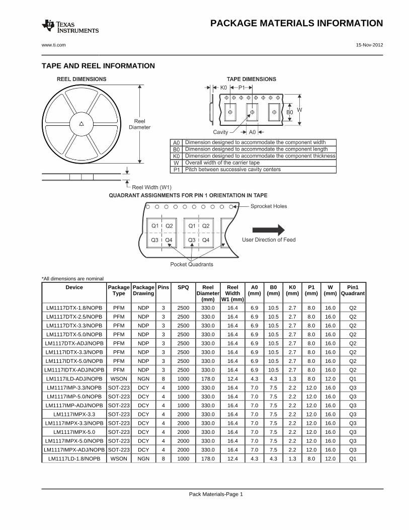
TAPE AND REEL INFORMATION
*All dimensions are nominal
Device PackageType
PackageDrawing
Pins SPQ ReelDiameter
(mm)
ReelWidth
W1 (mm)
A0(mm)
B0(mm)
K0(mm)
P1(mm)
W(mm)
Pin1Quadrant
LM1117DTX-1.8/NOPB PFM NDP 3 2500 330.0 16.4 6.9 10.5 2.7 8.0 16.0 Q2
LM1117DTX-2.5/NOPB PFM NDP 3 2500 330.0 16.4 6.9 10.5 2.7 8.0 16.0 Q2
LM1117DTX-3.3/NOPB PFM NDP 3 2500 330.0 16.4 6.9 10.5 2.7 8.0 16.0 Q2
LM1117DTX-5.0/NOPB PFM NDP 3 2500 330.0 16.4 6.9 10.5 2.7 8.0 16.0 Q2
LM1117DTX-ADJ/NOPB PFM NDP 3 2500 330.0 16.4 6.9 10.5 2.7 8.0 16.0 Q2
LM1117IDTX-3.3/NOPB PFM NDP 3 2500 330.0 16.4 6.9 10.5 2.7 8.0 16.0 Q2
LM1117IDTX-5.0/NOPB PFM NDP 3 2500 330.0 16.4 6.9 10.5 2.7 8.0 16.0 Q2
LM1117IDTX-ADJ/NOPB PFM NDP 3 2500 330.0 16.4 6.9 10.5 2.7 8.0 16.0 Q2
LM1117ILD-ADJ/NOPB WSON NGN 8 1000 178.0 12.4 4.3 4.3 1.3 8.0 12.0 Q1
LM1117IMP-3.3/NOPB SOT-223 DCY 4 1000 330.0 16.4 7.0 7.5 2.2 12.0 16.0 Q3
LM1117IMP-5.0/NOPB SOT-223 DCY 4 1000 330.0 16.4 7.0 7.5 2.2 12.0 16.0 Q3
LM1117IMP-ADJ/NOPB SOT-223 DCY 4 1000 330.0 16.4 7.0 7.5 2.2 12.0 16.0 Q3
LM1117IMPX-3.3 SOT-223 DCY 4 2000 330.0 16.4 7.0 7.5 2.2 12.0 16.0 Q3
LM1117IMPX-3.3/NOPB SOT-223 DCY 4 2000 330.0 16.4 7.0 7.5 2.2 12.0 16.0 Q3
LM1117IMPX-5.0 SOT-223 DCY 4 2000 330.0 16.4 7.0 7.5 2.2 12.0 16.0 Q3
LM1117IMPX-5.0/NOPB SOT-223 DCY 4 2000 330.0 16.4 7.0 7.5 2.2 12.0 16.0 Q3
LM1117IMPX-ADJ/NOPB SOT-223 DCY 4 2000 330.0 16.4 7.0 7.5 2.2 12.0 16.0 Q3
LM1117LD-1.8/NOPB WSON NGN 8 1000 178.0 12.4 4.3 4.3 1.3 8.0 12.0 Q1
PACKAGE MATERIALS INFORMATION
www.ti.com 15-Nov-2012
Pack Materials-Page 1
Device PackageType
PackageDrawing
Pins SPQ ReelDiameter
(mm)
ReelWidth
W1 (mm)
A0(mm)
B0(mm)
K0(mm)
P1(mm)
W(mm)
Pin1Quadrant
LM1117LD-2.5/NOPB WSON NGN 8 1000 178.0 12.4 4.3 4.3 1.3 8.0 12.0 Q1
LM1117LD-3.3/NOPB WSON NGN 8 1000 178.0 12.4 4.3 4.3 1.3 8.0 12.0 Q1
LM1117LD-ADJ/NOPB WSON NGN 8 1000 178.0 12.4 4.3 4.3 1.3 8.0 12.0 Q1
LM1117LDX-1.8 WSON NGN 8 4500 330.0 12.4 4.3 4.3 1.3 8.0 12.0 Q1
LM1117LDX-1.8/NOPB WSON NGN 8 4500 330.0 12.4 4.3 4.3 1.3 8.0 12.0 Q1
LM1117LDX-ADJ/NOPB WSON NGN 8 4500 330.0 12.4 4.3 4.3 1.3 8.0 12.0 Q1
LM1117MP-1.8/NOPB SOT-223 DCY 4 1000 330.0 16.4 7.0 7.5 2.2 12.0 16.0 Q3
LM1117MP-2.5/NOPB SOT-223 DCY 4 1000 330.0 16.4 7.0 7.5 2.2 12.0 16.0 Q3
LM1117MP-3.3/NOPB SOT-223 DCY 4 1000 330.0 16.4 7.0 7.5 2.2 12.0 16.0 Q3
LM1117MP-5.0/NOPB SOT-223 DCY 4 1000 330.0 16.4 7.0 7.5 2.2 12.0 16.0 Q3
LM1117MP-ADJ/NOPB SOT-223 DCY 4 1000 330.0 16.4 7.0 7.5 2.2 12.0 16.0 Q3
LM1117MPX-1.8/NOPB SOT-223 DCY 4 2000 330.0 16.4 7.0 7.5 2.2 12.0 16.0 Q3
LM1117MPX-2.5/NOPB SOT-223 DCY 4 2000 330.0 16.4 7.0 7.5 2.2 12.0 16.0 Q3
LM1117MPX-3.3/NOPB SOT-223 DCY 4 2000 330.0 16.4 7.0 7.5 2.2 12.0 16.0 Q3
LM1117MPX-5.0 SOT-223 DCY 4 2000 330.0 16.4 7.0 7.5 2.2 12.0 16.0 Q3
LM1117MPX-5.0/NOPB SOT-223 DCY 4 2000 330.0 16.4 7.0 7.5 2.2 12.0 16.0 Q3
LM1117MPX-ADJ/NOPB SOT-223 DCY 4 2000 330.0 16.4 7.0 7.5 2.2 12.0 16.0 Q3
LM1117SX-3.3/NOPB DDPAK/TO-263
KTT 3 500 330.0 24.4 10.75 14.85 5.0 16.0 24.0 Q2
LM1117SX-5.0/NOPB DDPAK/TO-263
KTT 3 500 330.0 24.4 10.75 14.85 5.0 16.0 24.0 Q2
LM1117SX-ADJ/NOPB DDPAK/TO-263
KTT 3 500 330.0 24.4 10.75 14.85 5.0 16.0 24.0 Q2
PACKAGE MATERIALS INFORMATION
www.ti.com 15-Nov-2012
Pack Materials-Page 2
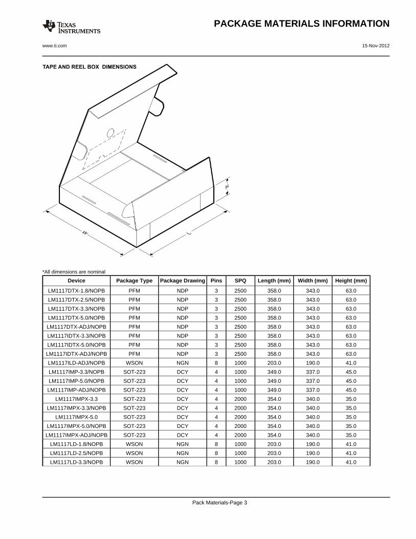
*All dimensions are nominal
Device Package Type Package Drawing Pins SPQ Length (mm) Width (mm) Height (mm)
LM1117DTX-1.8/NOPB PFM NDP 3 2500 358.0 343.0 63.0
LM1117DTX-2.5/NOPB PFM NDP 3 2500 358.0 343.0 63.0
LM1117DTX-3.3/NOPB PFM NDP 3 2500 358.0 343.0 63.0
LM1117DTX-5.0/NOPB PFM NDP 3 2500 358.0 343.0 63.0
LM1117DTX-ADJ/NOPB PFM NDP 3 2500 358.0 343.0 63.0
LM1117IDTX-3.3/NOPB PFM NDP 3 2500 358.0 343.0 63.0
LM1117IDTX-5.0/NOPB PFM NDP 3 2500 358.0 343.0 63.0
LM1117IDTX-ADJ/NOPB PFM NDP 3 2500 358.0 343.0 63.0
LM1117ILD-ADJ/NOPB WSON NGN 8 1000 203.0 190.0 41.0
LM1117IMP-3.3/NOPB SOT-223 DCY 4 1000 349.0 337.0 45.0
LM1117IMP-5.0/NOPB SOT-223 DCY 4 1000 349.0 337.0 45.0
LM1117IMP-ADJ/NOPB SOT-223 DCY 4 1000 349.0 337.0 45.0
LM1117IMPX-3.3 SOT-223 DCY 4 2000 354.0 340.0 35.0
LM1117IMPX-3.3/NOPB SOT-223 DCY 4 2000 354.0 340.0 35.0
LM1117IMPX-5.0 SOT-223 DCY 4 2000 354.0 340.0 35.0
LM1117IMPX-5.0/NOPB SOT-223 DCY 4 2000 354.0 340.0 35.0
LM1117IMPX-ADJ/NOPB SOT-223 DCY 4 2000 354.0 340.0 35.0
LM1117LD-1.8/NOPB WSON NGN 8 1000 203.0 190.0 41.0
LM1117LD-2.5/NOPB WSON NGN 8 1000 203.0 190.0 41.0
LM1117LD-3.3/NOPB WSON NGN 8 1000 203.0 190.0 41.0
PACKAGE MATERIALS INFORMATION
www.ti.com 15-Nov-2012
Pack Materials-Page 3
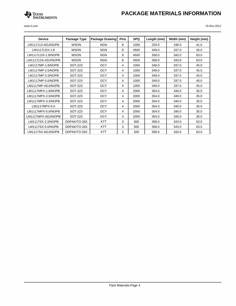
Device Package Type Package Drawing Pins SPQ Length (mm) Width (mm) Height (mm)
LM1117LD-ADJ/NOPB WSON NGN 8 1000 203.0 190.0 41.0
LM1117LDX-1.8 WSON NGN 8 4500 349.0 337.0 45.0
LM1117LDX-1.8/NOPB WSON NGN 8 4500 358.0 343.0 63.0
LM1117LDX-ADJ/NOPB WSON NGN 8 4500 358.0 343.0 63.0
LM1117MP-1.8/NOPB SOT-223 DCY 4 1000 349.0 337.0 45.0
LM1117MP-2.5/NOPB SOT-223 DCY 4 1000 349.0 337.0 45.0
LM1117MP-3.3/NOPB SOT-223 DCY 4 1000 349.0 337.0 45.0
LM1117MP-5.0/NOPB SOT-223 DCY 4 1000 349.0 337.0 45.0
LM1117MP-ADJ/NOPB SOT-223 DCY 4 1000 349.0 337.0 45.0
LM1117MPX-1.8/NOPB SOT-223 DCY 4 2000 354.0 340.0 35.0
LM1117MPX-2.5/NOPB SOT-223 DCY 4 2000 354.0 340.0 35.0
LM1117MPX-3.3/NOPB SOT-223 DCY 4 2000 354.0 340.0 35.0
LM1117MPX-5.0 SOT-223 DCY 4 2000 354.0 340.0 35.0
LM1117MPX-5.0/NOPB SOT-223 DCY 4 2000 354.0 340.0 35.0
LM1117MPX-ADJ/NOPB SOT-223 DCY 4 2000 354.0 340.0 35.0
LM1117SX-3.3/NOPB DDPAK/TO-263 KTT 3 500 358.0 343.0 63.0
LM1117SX-5.0/NOPB DDPAK/TO-263 KTT 3 500 358.0 343.0 63.0
LM1117SX-ADJ/NOPB DDPAK/TO-263 KTT 3 500 358.0 343.0 63.0
PACKAGE MATERIALS INFORMATION
www.ti.com 15-Nov-2012
Pack Materials-Page 4
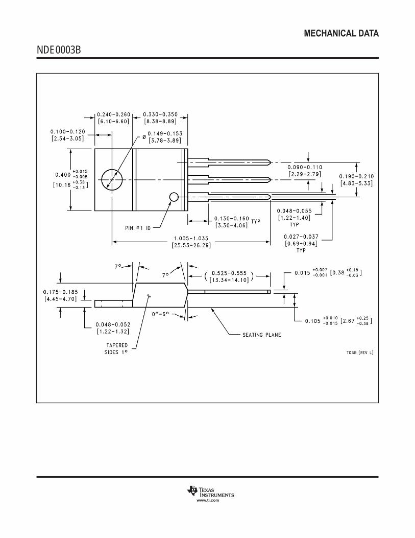
MECHANICAL DATA
NDE0003B
www.ti.com
MECHANICAL DATA
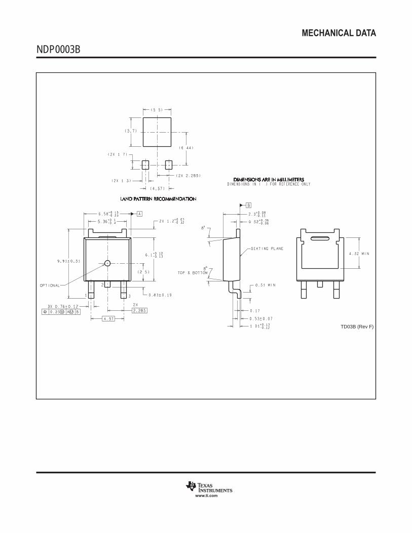
NDP0003B
www.ti.com
TD03B (Rev F)
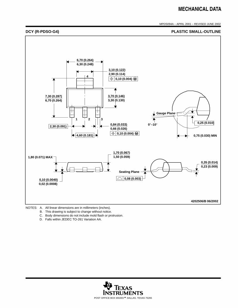
MECHANICAL DATA
MPDS094A – APRIL 2001 – REVISED JUNE 2002
POST OFFICE BOX 655303 • DALLAS, TEXAS 75265
DCY (R-PDSO-G4) PLASTIC SMALL-OUTLINE
4202506/B 06/2002
6,30 (0.248)6,70 (0.264)
2,90 (0.114)3,10 (0.122)
6,70 (0.264)7,30 (0.287) 3,70 (0.146)
3,30 (0.130)
0,02 (0.0008)0,10 (0.0040)
1,50 (0.059)1,70 (0.067)
0,23 (0.009)0,35 (0.014)
1 2 3
4
0,66 (0.026)0,84 (0.033)
1,80 (0.071) MAX
Seating Plane
0°–10°
Gauge Plane
0,75 (0.030) MIN
0,25 (0.010)
0,08 (0.003)
0,10 (0.004) M
2,30 (0.091)
4,60 (0.181) M0,10 (0.004)
NOTES: A. All linear dimensions are in millimeters (inches).B. This drawing is subject to change without notice.C. Body dimensions do not include mold flash or protrusion.D. Falls within JEDEC TO-261 Variation AA.

IMPORTANT NOTICE
Texas Instruments Incorporated and its subsidiaries (TI) reserve the right to make corrections, enhancements, improvements and otherchanges to its semiconductor products and services per JESD46, latest issue, and to discontinue any product or service per JESD48, latestissue. Buyers should obtain the latest relevant information before placing orders and should verify that such information is current andcomplete. All semiconductor products (also referred to herein as “components”) are sold subject to TI’s terms and conditions of salesupplied at the time of order acknowledgment.
TI warrants performance of its components to the specifications applicable at the time of sale, in accordance with the warranty in TI’s termsand conditions of sale of semiconductor products. Testing and other quality control techniques are used to the extent TI deems necessaryto support this warranty. Except where mandated by applicable law, testing of all parameters of each component is not necessarilyperformed.
TI assumes no liability for applications assistance or the design of Buyers’ products. Buyers are responsible for their products andapplications using TI components. To minimize the risks associated with Buyers’ products and applications, Buyers should provideadequate design and operating safeguards.
TI does not warrant or represent that any license, either express or implied, is granted under any patent right, copyright, mask work right, orother intellectual property right relating to any combination, machine, or process in which TI components or services are used. Informationpublished by TI regarding third-party products or services does not constitute a license to use such products or services or a warranty orendorsement thereof. Use of such information may require a license from a third party under the patents or other intellectual property of thethird party, or a license from TI under the patents or other intellectual property of TI.
Reproduction of significant portions of TI information in TI data books or data sheets is permissible only if reproduction is without alterationand is accompanied by all associated warranties, conditions, limitations, and notices. TI is not responsible or liable for such altereddocumentation. Information of third parties may be subject to additional restrictions.
Resale of TI components or services with statements different from or beyond the parameters stated by TI for that component or servicevoids all express and any implied warranties for the associated TI component or service and is an unfair and deceptive business practice.TI is not responsible or liable for any such statements.
Buyer acknowledges and agrees that it is solely responsible for compliance with all legal, regulatory and safety-related requirementsconcerning its products, and any use of TI components in its applications, notwithstanding any applications-related information or supportthat may be provided by TI. Buyer represents and agrees that it has all the necessary expertise to create and implement safeguards whichanticipate dangerous consequences of failures, monitor failures and their consequences, lessen the likelihood of failures that might causeharm and take appropriate remedial actions. Buyer will fully indemnify TI and its representatives against any damages arising out of the useof any TI components in safety-critical applications.
In some cases, TI components may be promoted specifically to facilitate safety-related applications. With such components, TI’s goal is tohelp enable customers to design and create their own end-product solutions that meet applicable functional safety standards andrequirements. Nonetheless, such components are subject to these terms.
No TI components are authorized for use in FDA Class III (or similar life-critical medical equipment) unless authorized officers of the partieshave executed a special agreement specifically governing such use.
Only those TI components which TI has specifically designated as military grade or “enhanced plastic” are designed and intended for use inmilitary/aerospace applications or environments. Buyer acknowledges and agrees that any military or aerospace use of TI componentswhich have not been so designated is solely at the Buyer's risk, and that Buyer is solely responsible for compliance with all legal andregulatory requirements in connection with such use.
TI has specifically designated certain components as meeting ISO/TS16949 requirements, mainly for automotive use. In any case of use ofnon-designated products, TI will not be responsible for any failure to meet ISO/TS16949.
Products Applications
Audio www.ti.com/audio Automotive and Transportation www.ti.com/automotive
Amplifiers amplifier.ti.com Communications and Telecom www.ti.com/communications
Data Converters dataconverter.ti.com Computers and Peripherals www.ti.com/computers
DLP® Products www.dlp.com Consumer Electronics www.ti.com/consumer-apps
DSP dsp.ti.com Energy and Lighting www.ti.com/energy
Clocks and Timers www.ti.com/clocks Industrial www.ti.com/industrial
Interface interface.ti.com Medical www.ti.com/medical
Logic logic.ti.com Security www.ti.com/security
Power Mgmt power.ti.com Space, Avionics and Defense www.ti.com/space-avionics-defense
Microcontrollers microcontroller.ti.com Video and Imaging www.ti.com/video
RFID www.ti-rfid.com
OMAP Applications Processors www.ti.com/omap TI E2E Community e2e.ti.com
Wireless Connectivity www.ti.com/wirelessconnectivity
Mailing Address: Texas Instruments, Post Office Box 655303, Dallas, Texas 75265Copyright © 2012, Texas Instruments Incorporated
Related Documents


