DEPARTMENT OF ELECTRONICS AND COMMUNICATION ENGINEERING LINEAR INTEGRATED CIRCUITS & MICROCONTROLLERS LAB Program/ Branch : B. E., / ECE Year / Semester : II/ IV Academic Year : 2020 – 2021 (Even Semester) Regulation : R 2017 HOD / ECE

Welcome message from author
This document is posted to help you gain knowledge. Please leave a comment to let me know what you think about it! Share it to your friends and learn new things together.
Transcript
DEPARTMENT OF ELECTRONICS AND COMMUNICATION ENGINEERING
LINEAR INTEGRATED CIRCUITS & MICROCONTROLLERS LAB
Program/ Branch : B. E., / ECE
Year / Semester : II/ IV
Academic Year : 2020 – 2021 (Even Semester)
Regulation : R 2017
HOD / ECE
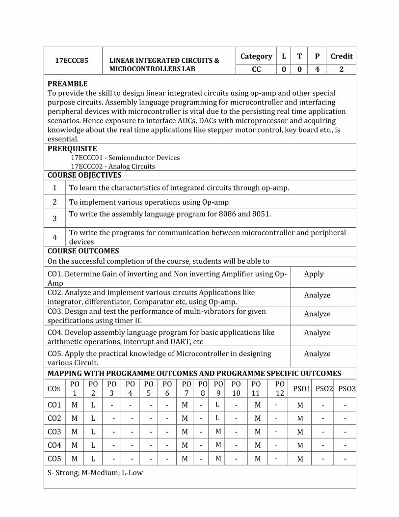
17ECCC85
LINEAR INTEGRATED CIRCUITS & MICROCONTROLLERS LAB
Category L T P Credit
CC 0 0 4 2
PREAMBLE To provide the skill to design linear integrated circuits using op-amp and other special purpose circuits. Assembly language programming for microcontroller and interfacing peripheral devices with microcontroller is vital due to the persisting real time application scenarios. Hence exposure to interface ADCs, DACs with microprocessor and acquiring knowledge about the real time applications like stepper motor control, key board etc., is essential. PRERQUISITE
17ECCC01 - Semiconductor Devices 17ECCC02 - Analog Circuits
COURSE OBJECTIVES
1 To learn the characteristics of integrated circuits through op-amp.
2 To implement various operations using Op-amp
3 To write the assembly language program for 8086 and 8051.
4 To write the programs for communication between microcontroller and peripheral devices
COURSE OUTCOMES
On the successful completion of the course, students will be able to
CO1. Determine Gain of inverting and Non inverting Amplifier using Op-Amp
Apply
CO2. Analyze and Implement various circuits Applications like integrator, differentiator, Comparator etc, using Op-amp.
Analyze
CO3. Design and test the performance of multi-vibrators for given specifications using timer IC
Analyze
CO4. Develop assembly language program for basic applications like arithmetic operations, interrupt and UART, etc
Analyze
CO5. Apply the practical knowledge of Microcontroller in designing various Circuit.
Analyze
MAPPING WITH PROGRAMME OUTCOMES AND PROGRAMME SPECIFIC OUTCOMES
COS PO 1
PO 2
PO 3
PO 4
PO 5
PO 6
PO 7
PO 8
PO 9
PO 10
PO 11
PO 12
PSO1 PSO2 PSO3
CO1 M L - - - - M - L - M - M - -
CO2 M L - - - - M - L - M - M - -
CO3 M L - - - - M - M - M - M - -
CO4 M L - - - - M - M - M - M - -
CO5 M L - - - - M - M - M - M - -
S- Strong; M-Medium; L-Low
LIST OF EXPERIMENTS:
LINEAR INTEGRATED CIRCUITS LAB Design 1. Inverting, Non-Inverting and Differential Amplifier.
2. Integrator, Differentiator, Comparator and Schmitt trigger.
3. Active LPF and HPF.
4. Astable and Monostable Multivibrators using IC 555
5. Voltage regulation using IC 723
MICROCONTROLLERS LAB
6. 8086 & 8051 Assembly language program for Arithmetic Operations.
7. 8051 Assembly language program for Logical, Interrupt & UART Operations.
8. Interfacing DAC to Microcontroller and generate Square, Triangular and Saw –tooth waveforms.
9. Interfacing ADC to Microcontroller.
10. Interfacing Stepper Motor to 8051 and operate it in Clockwise and Anti-Clockwise directions.
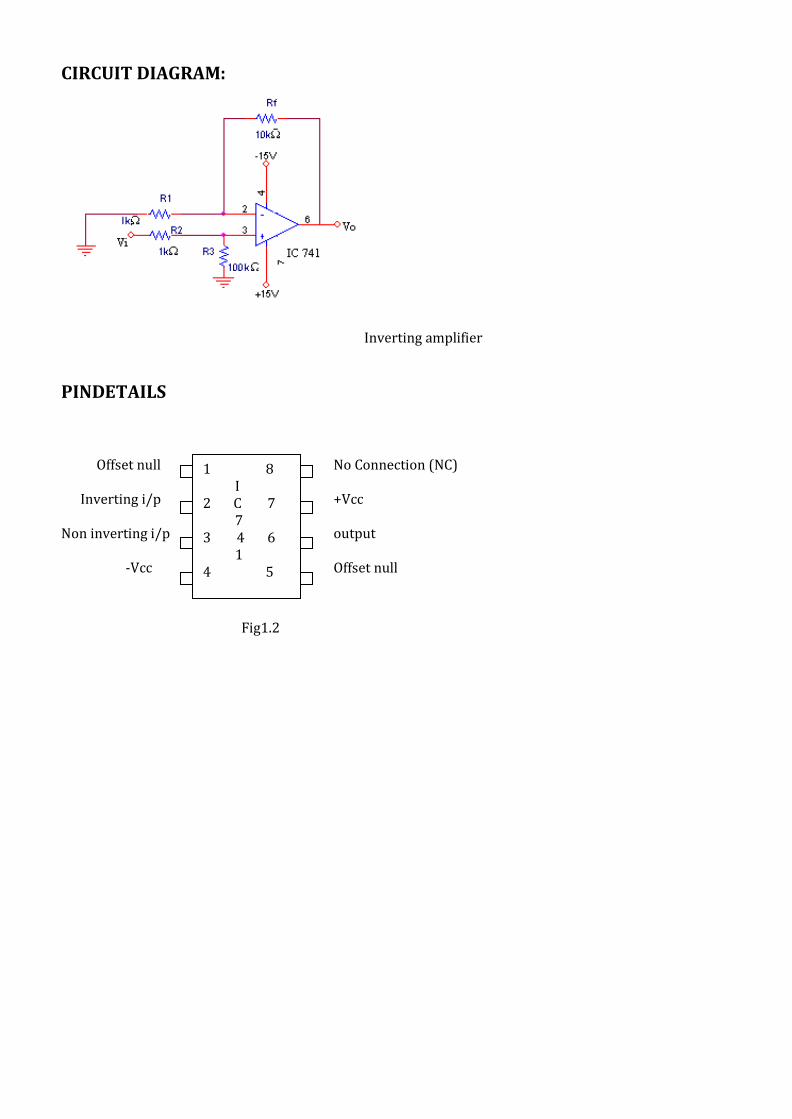
CIRCUIT DIAGRAM:
Inverting amplifier
PINDETAILS
Offset null No Connection (NC) Inverting i/p +Vcc Non inverting i/p output -Vcc Offset null
Fig1.2
1 8 I 2 C 7 7 3 4 6 1 4 5
1. INVERTING, NONINVERTING, AND DIFFERENTIAL AMPLIFIER
AIM: To study the operation of inverting, non-inverting and Differential amplifier using IC741.
APPRATUS REQUIRED:
S.NO COMPONENTS RANGE QUANTITY
1 Op-amp IC741 1
2 Resistor 1kΩ,10 kΩ 1
3 Bread board 1
4 Dual power supply (0-30)v 1
5 CRO (0-3) MHz) 1
6 Signal generator (0-3) MHZ 1
INVERTING AMPLIFIER:
THEORY:
An amplifier which provides a phase shift of 180º between input and output is called inverting
amplifier. The input signal is applied to the inverting terminal In this mode of operation the positive input terminal
of an amplifier is grounded and the input voltage is applied to the negative input terminal through resistor R1 .The
feedback applied through resistor Rf from the output to the negative input terminal. The output of such amplifier is
inverted as compared to the input terminal.
A=- Rf/R1
Rf=Feedback resistor R1= input resistor
PROCEDURE: 1. Connections are given as per the circuit diagram.
2. Connect the dual supply voltage of -15v and +15v to op-amp
3. Set the i/p voltage.
4. Using the probes obtain the input from the CRO. Tabulate the voltage and time period
5. using the probes obtain the output from the CRO .Tabulate the voltage and time Period, compare with the input.
6. Plot the graph between the voltage on the x axis and time period on the y axis.

MODEL GRAPH
I/P&O/P Waveforms TABULATION
Amplitude ( volts) Time period (ms)
Input
Output
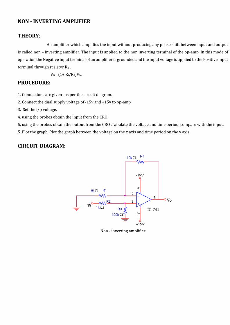
NON - INVERTING AMPLIFIER
THEORY:
An amplifier which amplifies the input without producing any phase shift between input and output
is called non – inverting amplifier. The input is applied to the non inverting terminal of the op-amp. In this mode of
operation the Negative input terminal of an amplifier is grounded and the input voltage is applied to the Positive input
terminal through resistor R1 .
VO= (1+ Rf/R1)VIn
PROCEDURE: 1. Connections are given as per the circuit diagram.
2. Connect the dual supply voltage of -15v and +15v to op-amp
3. Set the i/p voltage.
4. using the probes obtain the input from the CRO.
5. using the probes obtain the output from the CRO .Tabulate the voltage and time period, compare with the input.
5. Plot the graph. Plot the graph between the voltage on the x axis and time period on the y axis.
CIRCUIT DIAGRAM:
Non - inverting amplifier
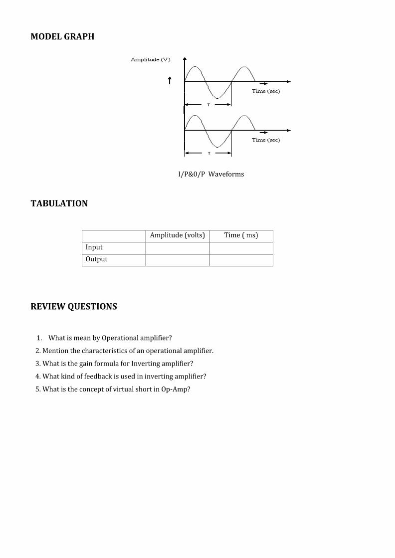
MODEL GRAPH
I/P&0/P Waveforms
TABULATION
Amplitude (volts) Time ( ms)
Input
Output
REVIEW QUESTIONS
1. What is mean by Operational amplifier?
2. Mention the characteristics of an operational amplifier.
3. What is the gain formula for Inverting amplifier?
4. What kind of feedback is used in inverting amplifier?
5. What is the concept of virtual short in Op-Amp?

CIRCUIT DIAGRAM
Differential Amplifier MODEL GRAPH
TABULATION
Amplitude (volts) Time ( ms)
Input
Output

RESULT:
Thus the inverting, non-inverting and Differential amplifier using IC741.
2. Integrator, Differentiator, Comparator and Schmitt trigger.
AIM: To study the operation of Integrator, Differentiator, Comparator and Schmitt Trigger using IC741.
APPRATUS REQUIRED:
S.NO COMPONENTS RANGE QUANTITY
1 Op-amp IC741 1
2 Resistor 1kΩ,10 kΩ 1
3 Bread board 1
4 Dual power supply (0-30)v 1
5 CRO (0-3) MHz) 1
6 Signal generator (0-3) MHZ 1
INTEGRATOR
THEORY In an integrator circuit, the output voltage is the integration of the input voltage. The integrator using
an active device like op – amp is called as an active integrator. The limitations of an ideal integrator can be minimized
by the practical integrator circuit which uses resistance in parallel with the capacitor.
A I circuit in which the output voltage waveform is the integral of the input voltage waveform is the
integrator or the integration amplifier.
Vo=1/R1C1 * t
0
vin dt +c
Vo = output voltage
R1 = input resistance
CF = feedback capacitor
vin = input voltage
PROCEDURE:
1. Connections are made as per the circuit diagram.
2. Connect the dual supply voltage of +15V and -15V to bias the Opamp.
3. A Sine wave of 1Vpp at 2KHz is given as input to pin 2.
4. A Sine wave of 1.5Vpp at 2KHz is given as input to pin 3.
4. using the probe obtain the Output waveform from the CRO.
5. Amplitude and time period readings are tabulated.
6. Plot the graph between the voltage on the x axis and time period on the y axis.
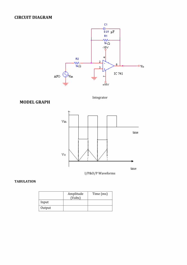
CIRCUIT DIAGRAM
Integrator
MODEL GRAPH
I/P&O/P Waveforms
TABULATION
Amplitude (Volts)
Time (ms)
Input
Output
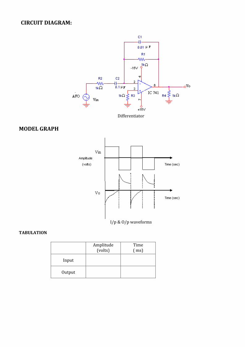
CIRCUIT DIAGRAM:
Differentiator
MODEL GRAPH
I/p & O/p waveforms
TABULATION
Amplitude
(volts) Time ( ms)
Input
Output

PIN DIAGRAM:
CIRCUIT DIAGRAM:
NON INVERTING COMPARATOR
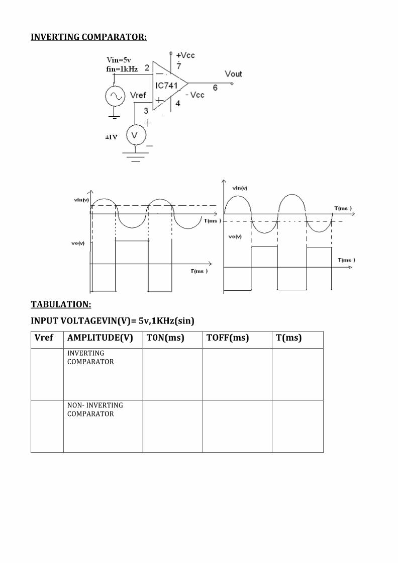
INVERTING COMPARATOR:
TABULATION:
INPUT VOLTAGEVIN(V)= 5v,1KHz(sin)
Vref AMPLITUDE(V) T0N(ms) TOFF(ms) T(ms)
INVERTING COMPARATOR
NON- INVERTING COMPARATOR
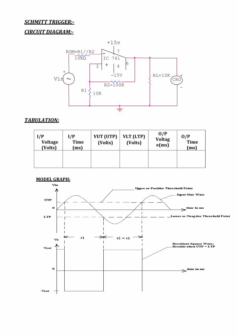
ROM=R1//R2 - 7
10KΩ IC 741
3
+
~
4 6
-15V RL=10K
R2=100K
R1
+ CRO
-
10K
SCHMITT TRIGGER:-
CIRCUIT DIAGRAM:-
+15v
Vin
TABULATION:
I/P Voltage (Volts)
I/P Time (ms)
VUT (UTP)
(Volts)
VLT (LTP)
(Volts)
O/P Voltage (ms)
O/P Time (ms)
MODEL GRAPH:

THEORY-(SCHMITT TRIGGER):-
A circuit which converts a irregular shaped waveform to a square wave or
pulse is called a Schmitt trigger or squaring circuit. The input voltage Vin triggers the
output Vo every time it exceeds certain voltage levels called upper threshold voltage VUT
and lower threshold voltage VLT. The threshold voltages are obtained by using the voltage
divider. A comparator with positive feedback is said to exhibit hysteresis, a dead band
condition. The hysteresis voltage is the difference between VUT & VLT.
There are two types of Schmitt trigger based on where the irregular wave is given.
They are, Inverting & non-inverting Schmitt trigger. Schmitt trigger finds application in
wave shaping circuits. The other name given to Schmitt trigger is regenerative
comparator.
RESULT:
Thus the Integrator, Differentiator and Schmitt Trigger circuit was constructed and the output
waveform was noted.
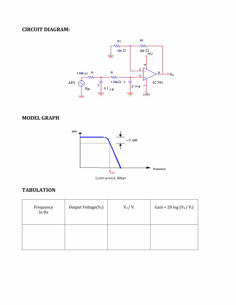
CIRCUIT DIAGRAM:
MODEL GRAPH
TABULATION
Frequency
In Hz
Output Voltage(V0)
V0 / Vi
Gain = 20 log (V0 / Vi)
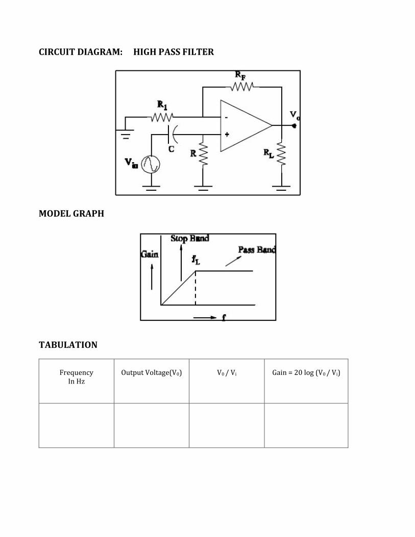
CIRCUIT DIAGRAM: HIGH PASS FILTER
MODEL GRAPH
TABULATION
Frequency
In Hz
Output Voltage(V0)
V0 / Vi
Gain = 20 log (V0 / Vi)

3. ACTIVE LPF AND HPF AIM:
To Design & Obtain the frequency response of a low pass and high pass filters having cutoff frequency
1 KHz and gain 3.
APPRATUS REQUIRED:
S.No COMPONENTS RANGE QUANTITY
1. Op –amp IC 741 1
2. Resistors 10KΩ, 20 KΩ,1.5 KΩ 1
3. Capacitor 0.1µf 1 4. Dual Power supply 0-30v
5. Cathode Ray Oscilloscope (0-30)MHz 1
6. Bread board 1
THEORY: A filter is a circuit that is designed to pass a specified band of frequency while attenuating
all the signals outside that band. Active filter circuits use the active elements such as op-amps, transistor
along the resistors and capacitors. A low pass filter has a constant gain from 0 Hz to a high cutoff frequency.
The frequency between 0Hz to fc2 are known as pass band frequencies where as the range of frequencies
those beyond fc2 are attenuated.
PROCEDURE:
1. Connections are made as per the Circuit diagram.
2. Connect the dual supply voltage of +15V and -15V to bias the Opamp.
3. A Sine wave is given as a input.
4. Vary the frequency, note down the corresponding output voltage.
5. The graph is drawn between the gain (y-axis) and the frequency (x-axis).
RESULT: Thus the Low pass and high pass filter circuit was constructed and the output Waveform was noted.
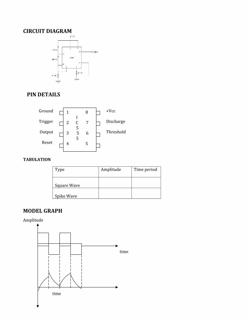
CIRCUIT DIAGRAM
PIN DETAILS Ground +Vcc Trigger Discharge Output Threshold Reset Control voltage TABULATION
MODEL GRAPH
Amplitude
time
time
Type
Amplitude Time period
Square Wave
Spike Wave
1 8 I 2 C 7 5 3 5 6 5 4 5
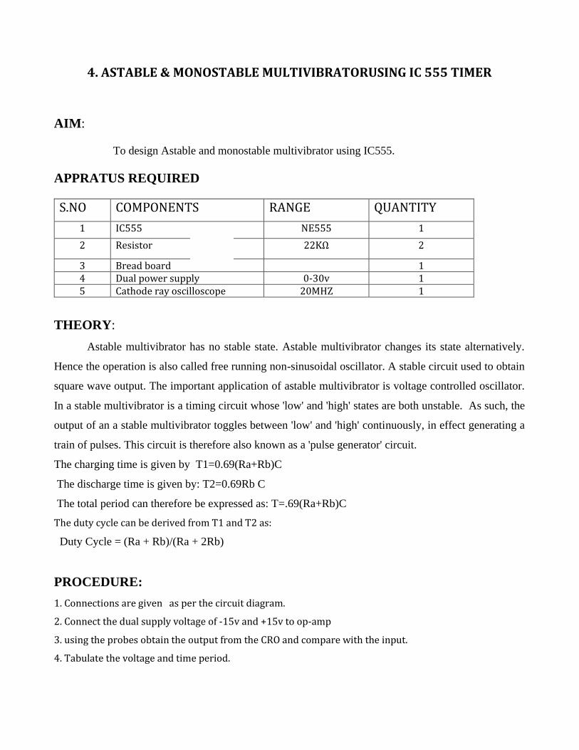
4. ASTABLE & MONOSTABLE MULTIVIBRATOR USING IC 555 TIMER
AIM:
To design Astable and monostable multivibrator using IC555.
APPRATUS REQUIRED
S.NO COMPONENTS RANGE QUANTITY
1 IC555 NE555 1
2 Resistor 22KΩ 2
3 Bread board 1 4 Dual power supply 0-30v 1 5 Cathode ray oscilloscope 20MHZ 1
THEORY:
Astable multivibrator has no stable state. Astable multivibrator changes its state alternatively.
Hence the operation is also called free running non-sinusoidal oscillator. A stable circuit used to obtain
square wave output. The important application of astable multivibrator is voltage controlled oscillator.
In a stable multivibrator is a timing circuit whose 'low' and 'high' states are both unstable. As such, the
output of an a stable multivibrator toggles between 'low' and 'high' continuously, in effect generating a
train of pulses. This circuit is therefore also known as a 'pulse generator' circuit.
The charging time is given by T1=0.69(Ra+Rb)C
The discharge time is given by: T2=0.69Rb C
The total period can therefore be expressed as: T=.69(Ra+Rb)C
The duty cycle can be derived from T1 and T2 as:
Duty Cycle = (Ra + Rb)/(Ra + 2Rb)
PROCEDURE:
1. Connections are given as per the circuit diagram.
2. Connect the dual supply voltage of -15v and +15v to op-amp
3. using the probes obtain the output from the CRO and compare with the input.
4. Tabulate the voltage and time period.
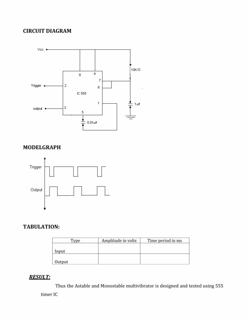
CIRCUIT DIAGRAM
MODELGRAPH
TABULATION:
RESULT:
Thus the Astable and Monostable multivibrator is designed and tested using 555
timer IC
Type Amplitude in volts Time period in ms Input
Output
CIRCUIT DIAGRAM:

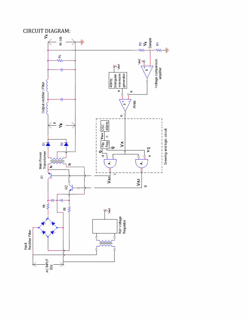
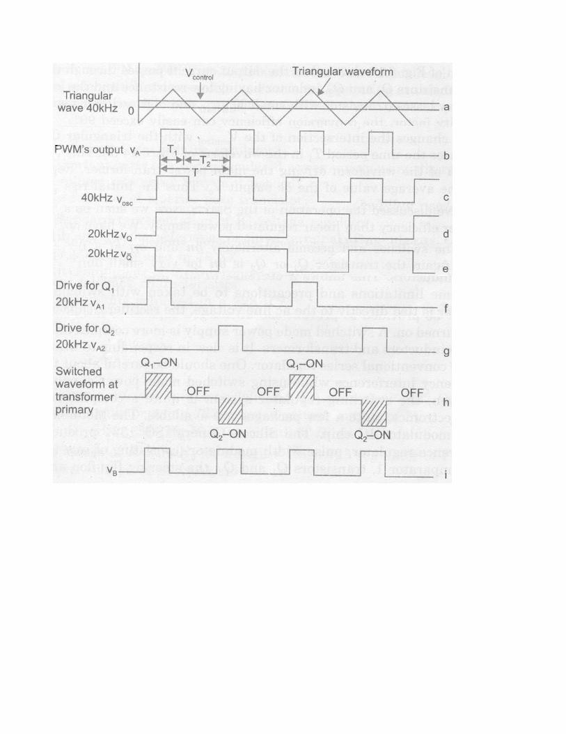
5 . VOLATAGE REGULATION USING IC 723
AIM :
To study the characteristics of volatage regulation using ic 723
THEORY:
Linear voltage regulator has some limitations. The input step-down transformer is bulky and most
expensive. At low frequency large values of filter capacitors are required to decrease the ripple. The input
voltage must be greater than the output voltage. So more power dissipated in the active region. SMPS
overcomes these difficulties.
The switching regulator is also called as switched mode regulator circuit. It is operated in a different
way from that of a conventional series regulator. The pass transistor is used as a controlled switch and is
operated in either in cutoff or saturation region. The power dissipation in the transistor is very small. So,
the efficiency of switched mode power supply is high.
The pulse width modulation is the basic principle of the switching regulators. The average value of
a repetitive pulse waveform depends on the area under the waveform.
Depending on the requirements, SMPS are used in the following various applications.
1. Adjustable high voltage constant current sources.
2. Telecommunication systems.
3. Battery powered systems.
4. Personal computers.
5. Video games.
6. Printers.
7. Motor and industrial control systems.
8. Automotive applications.
RESULT: Thus the characteristics of volatage regulation using ic 723 is studied

REVIEW QUESTIONS 1.What is a voltage regulator ? 2.Define load regulation. 3 Define line regulation. 4.Give the draw back of linear regulator. 5.What are the advantages of IC Voltage regulator.

MICROCONTROLLERS LAB
EX.NO: Date :
6. 8086 & 8051 Assembly language program for Arithmetic Operations.
AIM:
To write an ALP to perform Arithmetic operations using 8086 and 8051.
APPARATUS REQUIRED:
1. 8086 kit - 1
2. Power chord - 1
3. Keyboard - 1
4. 8051 kit - 1
i. DOUBLE PRECISION ADDITION:
ALGORITHM:
1. Start the program.
2. Load the addend’s value in some address.
3. Load the augend’s value in another address
4. Load the LSW of addend in some register
5. Add these values with LSW of the augends.
6. Move this value to a new address denoted as sum and stop the program.
PROGRAM:
RESULT OF DOUBLE PRECISION ADDITION:
INPUT: OUTPUT:
1100H – 12H 1200H – 47H
1101H - 34H 1201H – 41H
1102H – 56H 1202H – C8H
1103H – ABH 1203H - FCH
1104H – 34H, 1105H – 0DH, 1106H – 72H, 1107H – 51H
ADDRESS LABEL OPCODE MNEMONICS OPERAND COMMENTS
1000 MOV AX, [1100] Move data1 to ax
register 1003 ADD AX, [1104] Add data 1 and
data 2 1007 MOV [1200], AX Move the content
of acc 100A MOV AX, [1102] Move the content
of 1200H to AX 100D ADC AX, [1106] Add 1106H
content with AX
and store result in
AX
1011 MOV [1202], AX Move the AX
content to 1202H 1014 LAHF Load acc content
with HF 1015 MOV [1204], AH Move AH content
to specified
address. 1019 HLT Stop the program
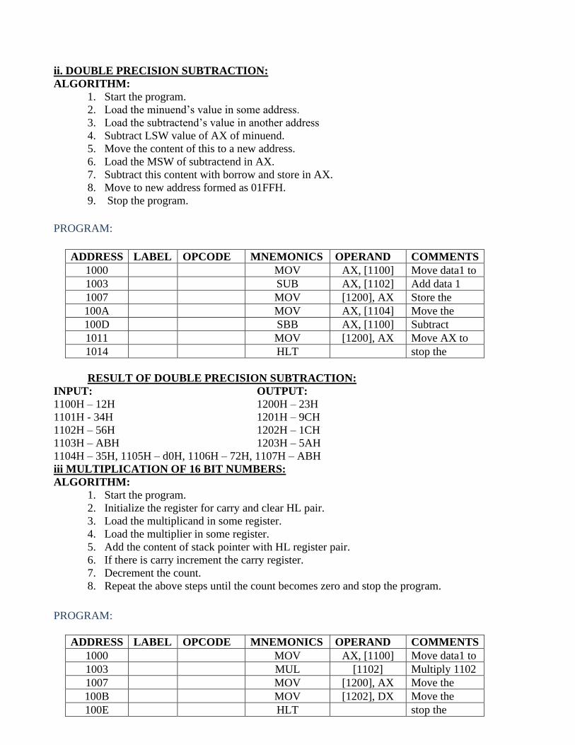
ii. DOUBLE PRECISION SUBTRACTION:
ALGORITHM:
1. Start the program.
2. Load the minuend’s value in some address.
3. Load the subtractend’s value in another address
4. Subtract LSW value of AX of minuend.
5. Move the content of this to a new address.
6. Load the MSW of subtractend in AX.
7. Subtract this content with borrow and store in AX.
8. Move to new address formed as 01FFH.
9. Stop the program.
PROGRAM:
ADDRESS LABEL OPCODE MNEMONICS OPERAND COMMENTS
1000 MOV AX, [1100] Move data1 to
ax register 1003 SUB AX, [1102] Add data 1
and data 2 1007 MOV [1200], AX Store the
result 100A MOV AX, [1104] Move the
MSW from
1104H to AX 100D SBB AX, [1100] Subtract
content of
1100H from
AX with
borrow
1011 MOV [1200], AX Move AX to
1200H 1014 HLT stop the
program
RESULT OF DOUBLE PRECISION SUBTRACTION:
INPUT: OUTPUT:
1100H – 12H 1200H – 23H
1101H - 34H 1201H – 9CH
1102H – 56H 1202H – 1CH
1103H – ABH 1203H – 5AH
1104H – 35H, 1105H – d0H, 1106H – 72H, 1107H – ABH
iii MULTIPLICATION OF 16 BIT NUMBERS:
ALGORITHM:
1. Start the program.
2. Initialize the register for carry and clear HL pair.
3. Load the multiplicand in some register.
4. Load the multiplier in some register.
5. Add the content of stack pointer with HL register pair.
6. If there is carry increment the carry register.
7. Decrement the count.
8. Repeat the above steps until the count becomes zero and stop the program.
PROGRAM:
ADDRESS LABEL OPCODE MNEMONICS OPERAND COMMENTS
1000 MOV AX, [1100] Move data1 to
ax register 1003 MUL [1102] Multiply 1102
content with
content of
1100
1007 MOV [1200], AX Move the
content of AX
to 1200 100B MOV [1202], DX Move the
content of DX
to 1202 100E HLT stop the
program

RESULT OF MULTIPLICATION:
INPUT: OUTPUT:
1100H – 04H 1200H – 06H
1101H - 03H 1201H – 00H
1102H – 01H 1202H – 04H
1103H – 02H 1203H – 06H
iv. DIVISION OF 32 BIT NUMBERS:
ALGORITHM:
1. Start the program.
2. Get the MSW of the dividend in the memory and the LSW in another register.
3. Get the divisor and divide the dividend by divisor.
4. Store the quotient and remainder.
5. Stop the program.
PROGRAM:
ADDRESS LABEL OPCODE MNEMONICS OPERAND COMMENTS
1000 MOV AX, [1100] Move data1 to
ax register 1004 MOV BX, [1102] Move data2 to
bx register 1007 DIV BX Divide
content of Ax
& BX and
store in DX &
AX
100B MOV [1200], AX Move the
content of AX
to 1200H 100E MOV [1202], DX Move the
content of AX
to 1202H 1012 HLT Stop the
program
RESULT OF DIVISION WITHOUT REMAINDER:
INPUT: OUTPUT:
1100H – 10H 1200H – FAH
1101H - 11H 1201H – FFH
1102H – 90H 1202H – 00H
1103H – 99H 1203H – 00H
1104H – 11H, 1105H – 11H
RESULT OF DIVISION WITH REMAINDER:
INPUT: OUTPUT:
1100H – 10H 1200H – FAH
1101H - 11H 1201H – FFH
1102H – 9CH 1202H – 02H
1103H – 99H 1203H – 00H
1104H – 11H, 1105H – 11H
ARITHMETIC OPERATION:
i. 16 BIT ADDITION:
ALGORITHM:
1. Start the program.
2. Get the MSB of 1st and 2nd operands.
3. Add the MSB and store the result in memory
4. Get the LSB of 1st and 2nd operands.
5. Add the LSB of the two operands and store it in memory.

6. Stop the program.
PROGRAM:
ADDRESS LABEL OPCODE MNEMON
ICS
OPERAND COMMENTS
4100 CLR C Clear carry
4101 MOV A, #DATA1 Move data1 to acc
4103 ADD A, #DATA2 Add data2 with acc
4105 MOV DPTR, #4150h Move content in
4500 to DPTR. 4108 MOVX @DPTR, A Move data to DPTR
location 4109 INC DPTR Increment DPTR
410A MOV A, #DATA1 Move data1 to acc
410C ADDC A, #DATA2 Add with carry
410E MOVX @DPTR, A Move data to dp
location 410F HERE SJMP: HERE
RESULT OF 16 BIT ADDITIONS:
INPUT:
OUTPUT:
4102H – 67H
4150H – ECH
4104H – 67H
4151H – F7H
410BH – 67H
ii. 8 BIT SUBTRACTION:
ALGORITHM:
1. Start the program and clear the carry flag and get first operand in accumulator.
2. Set the 2nd operand and subtract it from accumulator.
3. Store the result in memory.
4. Stop the program.
PROGRAM:
ADDRESS LABEL OPCODE MNEMONICS OPERAND COMMENTS
4100 CLR C Clear carry
4101 MOV A, #DATA1 Move data1 to acc
4103 SUBB A, #DATA2 Add data2 with acc
4105 MOV DPTR,
#4500h
Move content in
4500 to DPTR. 4108 MOVX @DPTR, A Move acc value to
DPTR location 4109 HER SJMP: HER
RESULT OF 8 BIT SUBTRACTION WITHOUT CARRY:
INPUT: OUTPUT:

4102H=68H 4152H = 10H
4104H=54H 4153H = 00H
RESULT OF 8 BIT SUBTRACTIONS WITH CARRY:
INPUT: OUTPUT: 4150H= 57H 4152H = F1H
4151H= 66H 4153H = F9H(C)
iii. 8 BIT MULTIPLICATION:
ALGORITHM:
1. Start the program.
2. Get 1st operand in A and 2nd in B.
3. Multiply A and B contents using multiplication instruction.
4. Store the result in memory.
5. Stop the program.
PROGRAM:
ADDRESS LABEL OPCODE MNEMONICS OPERAND COMMENTS
4100 MOV A, #DATA1 Move data1 to acc
4102 MOV B, #DATA1 Move data1 to acc
4105 MUL AB Add data2 with acc
4106 MOV DPTR,
#4500h
Move content in
4500 to DPTR. 4109 MOVX @DPTR, A Move acc value to
DPTR location 410A INC DPTR INC DPTR
410B MOV A, B Move B register
value to acc 410D MOVX @DPTR, A Move acc value to
DPTR location 410E HER SJMP: HER
RESULT OF 8 BIT MULTIPLICATIONS:
INPUT: OUTPUT:
4101H=0AH
4500H = 50H
4104H=88H
4501H = 05H
iv. 8 BIT DIVISION:
ALGORITHM:
1. Start the program.
2. Get 1st operand in A and 2nd in B.
3. Divide A by B contents using division instruction.
4. Store the result in memory.
5. Stop the program.
PROGRAM:
ADDRESS LABEL OPCODE MNEMONICS OPERAND COMMENTS
4100 MOV A, #DATA1 Move data1 to acc
4102 MOV B, #DATA1 Move data1 to acc
4105 DIV AB Divide A by B
4106 MOV DPTR,
#4500h
Move content in
4500H to DPTR. 4109 MOVX @DPTR, A Move acc value to
DPTR location 410A INC DPTR Inc DPTR
410B MOV A, B Move B register
value to acc 410D MOVX @DPTR, A Move acc value to
DPTR location 410E HER SJMP: HER
RESULT OF 8 BIT DIVISION WITHOUT REMAINDER:
INPUT: OUTPUT:
4101H=53H 4500H = 02H
4103H=23H 4501H = 10H
RESULT OF 8 BIT DIVISIONS WITH REMAINDER:
INPUT: OUTPUT:
4101H=06H
4500H = 02H
4103H=03H
RESULT:

6. 8051 Assembly language program for Logical, Interrupt & UART Operations.
AIM:
To write an assembly language program for the Logical, Interrupt & UART Operations using 8051.
APPARATUS REQUIRED:
1. 8051 kit - 1
2. Power chord - 1
3. Keyboard - 1
LOGICAL OPERATION:
i. OR OPERATION:
ALGORITHM:
1. Start the program.
2. Get 1st operand in Accumulator.
3. Get 2nd operand and OR it with accumulator content.
4. Store the result in memory.
5. Stop the program.
PROGRAM:
ADDRESS LABEL OPCODE MNEMONICS OPERAND COMMENTS
4100 MOV A, #DATA1 Move data1 to acc
4101 ORL A, #DATA2 Add data2 with acc
4103 MOV DPTR,
#4500H
Move content in
4500H to DPTR. 4105 MOVX @DPTR, A Move acc value to
DPTR location 4108 HER SJMP: HER
RESULT OF OR OPERATION:
INPUT: OUTPUT:
4101H=79H
4500H = FDH
4103H=ACH
ii. AND OPERATION:
ALGORITHM:
1. Start the program.
2. Get 1st operand in Accumulator.
3. Get 2nd operand and AND it with accumulator content.
4. Store the result in memory.
5. Stop the program.
PROGRAM:
ADDRESS LABEL OPCODE MNEMONICS OPERAND COMMENTS
4100 MOV A, #DATA1 Move data1 to acc
4101 ANL A, #DATA2 Add data2 with acc
4103 MOV DPTR,
#4500H
Move content in
4500H to DPTR. 4105 MOVX @DPTR, A Move acc value to
DPTR location 4108 HER SJMP: HER
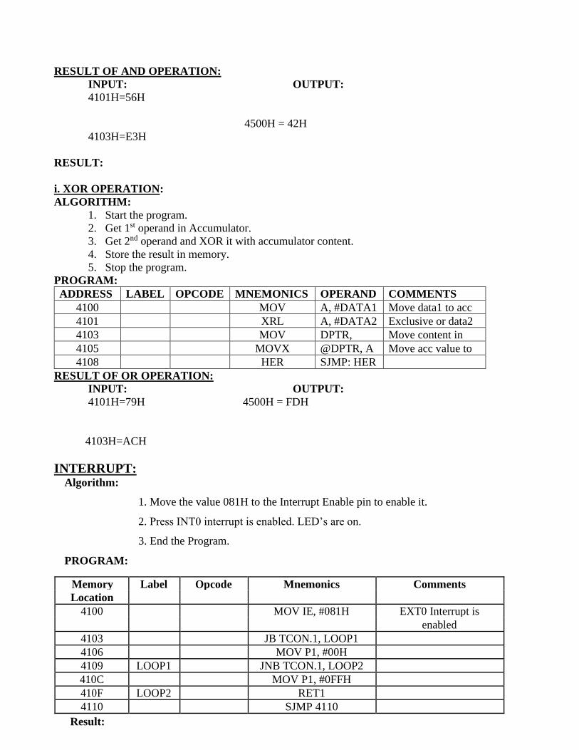
RESULT OF AND OPERATION:
INPUT: OUTPUT:
4101H=56H
4500H = 42H
4103H=E3H
RESULT:
i. XOR OPERATION:
ALGORITHM:
1. Start the program.
2. Get 1st operand in Accumulator.
3. Get 2nd operand and XOR it with accumulator content.
4. Store the result in memory.
5. Stop the program.
PROGRAM:
ADDRESS LABEL OPCODE MNEMONICS OPERAND COMMENTS
4100 MOV A, #DATA1 Move data1 to acc
4101 XRL A, #DATA2 Exclusive or data2
with acc 4103 MOV DPTR,
#4500H
Move content in
4500H to DPTR. 4105 MOVX @DPTR, A Move acc value to
DPTR location 4108 HER SJMP: HER
RESULT OF OR OPERATION:
INPUT: OUTPUT:
4101H=79H 4500H = FDH
4103H=ACH
INTERRUPT: Algorithm:
1. Move the value 081H to the Interrupt Enable pin to enable it.
2. Press INT0 interrupt is enabled. LED’s are on.
3. End the Program.
PROGRAM:
Memory Label Opcode Mnemonics Comments
Location
4100 MOV IE, #081H EXT0 Interrupt is
enabled
4103 JB TCON.1, LOOP1
4106 MOV P1, #00H
4109 LOOP1 JNB TCON.1, LOOP2
410C MOV P1, #0FFH
410F LOOP2 RET1
4110 SJMP 4110 Result:

8. Interfacing DAC to Microcontroller and generate Square, Triangular and Saw –tooth waveforms.
AIM:
To interface DAC with 8051 to demonstrate the generation of square, saw tooth and
triangular wave.
APPARATUS REQUIRED:
SL.NO ITEM SPECIFICATION QUANTITY
1 Microprocessor kit 4185,Vi Microsystems 1
2 Power supply +5 V dc 1
3 DAC Interface board Vi Microsystems 1
ALGORITHM:
(a) SQUARE WAVE GENERATION: 1. Load the initial value (00) to Accumulator and move it to DAC.
2. Call the delay program
3. Load the final value (FF) to accumulator and move it to DAC.
4. Call the delay program.
5. Repeat steps 2 to 5. WAVEFORM
OBSERVATION:
WAVE FORMS AMPLITUDE TIME PERIOD
Square waveform
Saw tooth waveform
Triangular waveform
Program:

(b) SAW TOOTH GENERATION 1. Load the initial value (00) to Accumulator
2. Move the accumulator content to DAC.
3. Increment the accumulator content by 1.
4. Repeat steps 3 and 4.
(c) TRIANGULAR WAVE GENERATION 1. Load the initial value (00) to Accumulator.
2. Move the accumulator content to DAC
3. Increment the accumulator content by 1.
4. If accumulator content is zero proceed to next step. Else go to step 3.
5. Load value (FF) to accumulator.
6. Move the accumulator content to DAC.
7. Decrement the accumulator content by 1.
8. If accumulator content is zero go to step 2. Else go to step 2.
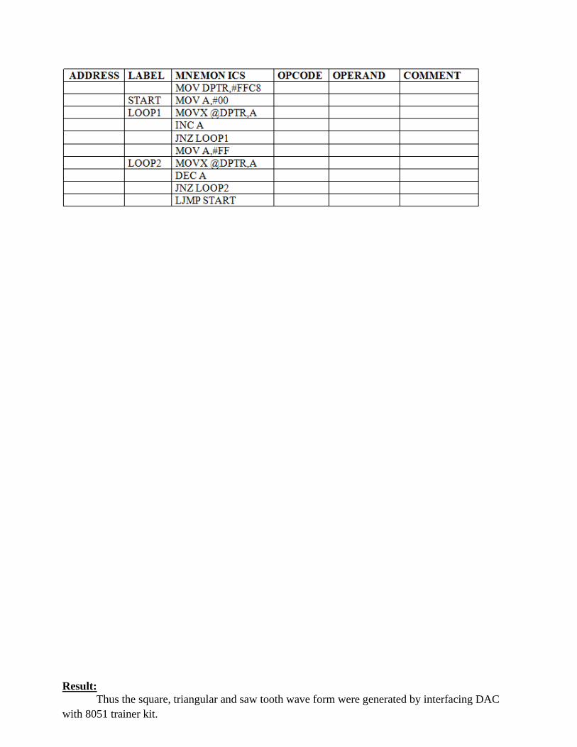
Result: Thus the square, triangular and saw tooth wave form were generated by interfacing DAC
with 8051 trainer kit.
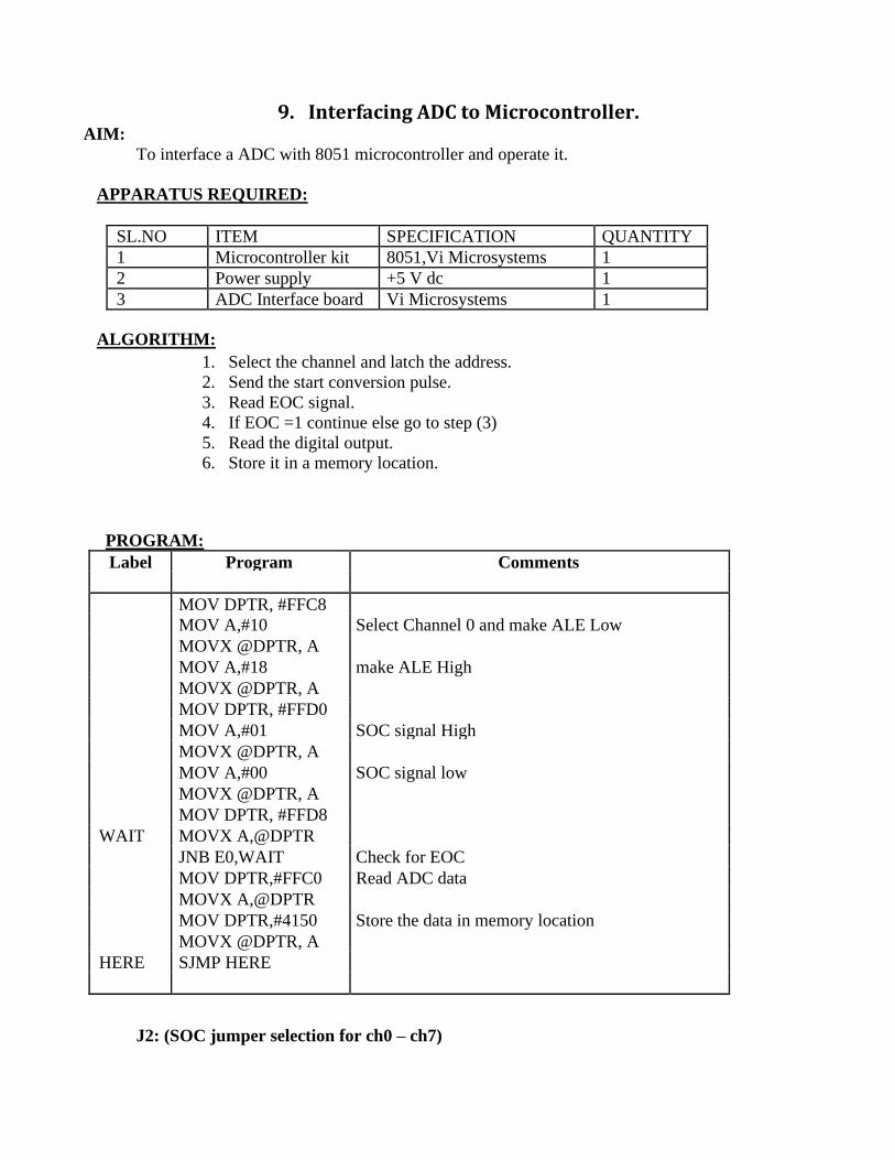
9. Interfacing ADC to Microcontroller. AIM:
To interface a ADC with 8051 microcontroller and operate it.
APPARATUS REQUIRED:
SL.NO ITEM SPECIFICATION QUANTITY
1 Microcontroller kit 8051,Vi Microsystems 1
2 Power supply +5 V dc 1
3 ADC Interface board Vi Microsystems 1
ALGORITHM: 1. Select the channel and latch the address.
2. Send the start conversion pulse.
3. Read EOC signal.
4. If EOC =1 continue else go to step (3)
5. Read the digital output. 6. Store it in a memory location.
PROGRAM:
Label Program Comments
MOV DPTR, #FFC8
MOV A,#10 Select Channel 0 and make ALE Low
MOVX @DPTR, A
MOV A,#18 make ALE High
MOVX @DPTR, A
MOV DPTR, #FFD0
MOV A,#01 SOC signal High
MOVX @DPTR, A
MOV A,#00 SOC signal low
MOVX @DPTR, A
MOV DPTR, #FFD8
WAIT MOVX A,@DPTR
JNB E0,WAIT Check for EOC
MOV DPTR,#FFC0 Read ADC data
MOVX A,@DPTR
MOV DPTR,#4150 Store the data in memory location
MOVX @DPTR, A
HERE SJMP HERE
J2: (SOC jumper selection for ch0 – ch7)
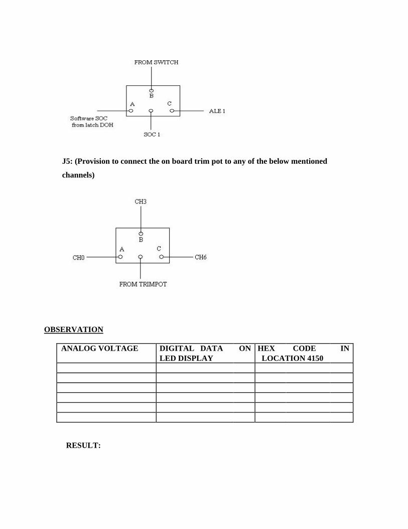
J5: (Provision to connect the on board trim pot to any of the below mentioned
channels)
OBSERVATION
ANALOG VOLTAGE DIGITAL DATA ON HEX CODE IN
LED DISPLAY LOCATION 4150
RESULT:
10. Interfacing Stepper Motor to 8051 and operate it in Clockwise and Anti-Clockwise directions.
AIM:
To interface a stepper motor with 8051 microcontroller and operate it.
THEORY:
A motor in which the rotor is able to assume only discrete stationary angular position is a stepper
motor. The rotary motion occurs in a step-wise manner from one equilibrium position to the next. Stepper
Motors are used very wisely in position control systems like printers, disk drives, process control
machine tools, etc.
The basic two-phase stepper motor consists of two pairs of stator poles. Each of the four poles
has its own winding. The excitation of any one winding generates a North Pole. A South Pole gets
induced at the diametrically opposite side. The rotor magnetic system has two end faces. It is a permanent
magnet with one face as South Pole and the other as North Pole.
The Stepper Motor windings A1, A2, B1, B2 are cyclically excited with a DC current to run the
motor in clockwise direction. By reversing the phase sequence as A1, B2, A2, B1, anticlockwise stepping
can be obtained.
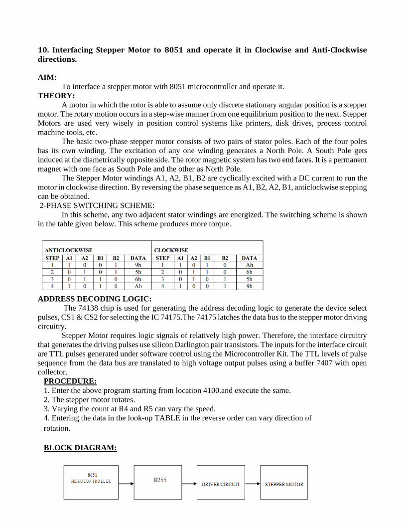
2-PHASE SWITCHING SCHEME:
In this scheme, any two adjacent stator windings are energized. The switching scheme is shown
in the table given below. This scheme produces more torque.
ADDRESS DECODING LOGIC:
The 74138 chip is used for generating the address decoding logic to generate the device select
pulses, CS1 & CS2 for selecting the IC 74175.The 74175 latches the data bus to the stepper motor driving
circuitry.
Stepper Motor requires logic signals of relatively high power. Therefore, the interface circuitry
that generates the driving pulses use silicon Darlington pair transistors. The inputs for the interface circuit
are TTL pulses generated under software control using the Microcontroller Kit. The TTL levels of pulse
sequence from the data bus are translated to high voltage output pulses using a buffer 7407 with open
collector.
PROCEDURE: 1. Enter the above program starting from location 4100.and execute the same.
2. The stepper motor rotates.
3. Varying the count at R4 and R5 can vary the speed.
4. Entering the data in the look-up TABLE in the reverse order can vary direction of
rotation.
BLOCK DIAGRAM:

Address OPCODES
Label
MNEM
OPERAND
Comments ONICS
ORG 4100h
4100 START MOV DPTR, #TABLE Load the start address
of switching scheme
data TABLE into Data
Pointer (DPTR)
4103 MOV R0, #04 Load the count in R0
4105 LOOP: MOVX A, @DPTR Load the number in
TABLE into A
4106 PUSH DPH Push DPTR value to
4108 PUSH DPL Stack
410A MOV DPTR, #0FFC0h Load the Motor port
address into DPTR
410D MOVX @DPTR, A Send the value in A to
stepper Motor port
address
410E MOV R4, #0FFh Delay loop to cause a
4110 DELA MOV R5, #0FFh specific amount of
Y: time delay before next
data item is sent to the 4112 DELA DJNZ R5, DELAY1
Y1: Motor
4114 DJNZ R4, DELAY
4116 POP DPL POP back DPTR value
4118 POP DPH from Stack
411A INC DPTR Increment DPTR to
point to next item in
the table
411B DJNZ R0, LOOP Decrement R0, if not
zero repeat the loop
411D SJMP START Short jump to Start of
the program to make
the motor rotate
continuously
411F TABLE DB 09 05 06 0Ah Values as per two-
: phase switching
scheme
RESULT:
Thus a stepper motor was interfaced with 8051 and run in forward and reverse
directions at various speeds.
Related Documents